KR102164941B1 - Thin film transistor substrate, display apparatus including the same, and manufacturing method of the thin film transistor substrate - Google Patents
Thin film transistor substrate, display apparatus including the same, and manufacturing method of the thin film transistor substrateDownload PDFInfo
- Publication number
- KR102164941B1 KR102164941B1KR1020140004081AKR20140004081AKR102164941B1KR 102164941 B1KR102164941 B1KR 102164941B1KR 1020140004081 AKR1020140004081 AKR 1020140004081AKR 20140004081 AKR20140004081 AKR 20140004081AKR 102164941 B1KR102164941 B1KR 102164941B1
- Authority
- KR
- South Korea
- Prior art keywords
- layer
- oxide semiconductor
- thin film
- film transistor
- transistor substrate
- Prior art date
- Legal status (The legal status is an assumption and is not a legal conclusion. Google has not performed a legal analysis and makes no representation as to the accuracy of the status listed.)
- Active
Links
- 239000000758substrateSubstances0.000titleclaimsabstractdescription85
- 239000010409thin filmSubstances0.000titleclaimsabstractdescription64
- 238000004519manufacturing processMethods0.000titleclaimsabstractdescription19
- 239000004065semiconductorSubstances0.000claimsabstractdescription67
- 238000000034methodMethods0.000claimsabstractdescription54
- 238000010438heat treatmentMethods0.000claimsabstractdescription30
- 239000000463materialSubstances0.000claimsdescription41
- 229920002120photoresistant polymerPolymers0.000claimsdescription33
- 239000010408filmSubstances0.000claimsdescription28
- 239000010949copperSubstances0.000claimsdescription16
- PXHVJJICTQNCMI-UHFFFAOYSA-NNickelChemical compound[Ni]PXHVJJICTQNCMI-UHFFFAOYSA-N0.000claimsdescription15
- 239000011651chromiumSubstances0.000claimsdescription14
- 239000011572manganeseSubstances0.000claimsdescription14
- RYGMFSIKBFXOCR-UHFFFAOYSA-NCopperChemical compound[Cu]RYGMFSIKBFXOCR-UHFFFAOYSA-N0.000claimsdescription12
- 230000004888barrier functionEffects0.000claimsdescription12
- 229910052802copperInorganic materials0.000claimsdescription12
- 238000000151depositionMethods0.000claimsdescription11
- 239000011777magnesiumSubstances0.000claimsdescription10
- 239000010955niobiumSubstances0.000claimsdescription10
- ZOKXTWBITQBERF-UHFFFAOYSA-NMolybdenumChemical compound[Mo]ZOKXTWBITQBERF-UHFFFAOYSA-N0.000claimsdescription9
- 229910052750molybdenumInorganic materials0.000claimsdescription9
- 239000011733molybdenumSubstances0.000claimsdescription9
- 229910000881Cu alloyInorganic materials0.000claimsdescription8
- 230000008021depositionEffects0.000claimsdescription8
- VYZAMTAEIAYCRO-UHFFFAOYSA-NChromiumChemical compound[Cr]VYZAMTAEIAYCRO-UHFFFAOYSA-N0.000claimsdescription7
- PWHULOQIROXLJO-UHFFFAOYSA-NManganeseChemical compound[Mn]PWHULOQIROXLJO-UHFFFAOYSA-N0.000claimsdescription7
- 229910052804chromiumInorganic materials0.000claimsdescription7
- 239000004973liquid crystal related substanceSubstances0.000claimsdescription7
- 229910052748manganeseInorganic materials0.000claimsdescription7
- 229910052715tantalumInorganic materials0.000claimsdescription7
- GUVRBAGPIYLISA-UHFFFAOYSA-Ntantalum atomChemical compound[Ta]GUVRBAGPIYLISA-UHFFFAOYSA-N0.000claimsdescription7
- XLOMVQKBTHCTTD-UHFFFAOYSA-Nzinc oxideInorganic materials[Zn]=OXLOMVQKBTHCTTD-UHFFFAOYSA-N0.000claimsdescription7
- 239000011787zinc oxideSubstances0.000claimsdescription7
- GYHNNYVSQQEPJS-UHFFFAOYSA-NGalliumChemical compound[Ga]GYHNNYVSQQEPJS-UHFFFAOYSA-N0.000claimsdescription5
- FYYHWMGAXLPEAU-UHFFFAOYSA-NMagnesiumChemical compound[Mg]FYYHWMGAXLPEAU-UHFFFAOYSA-N0.000claimsdescription5
- ATJFFYVFTNAWJD-UHFFFAOYSA-NTinChemical compound[Sn]ATJFFYVFTNAWJD-UHFFFAOYSA-N0.000claimsdescription5
- 229910017052cobaltInorganic materials0.000claimsdescription5
- 239000010941cobaltSubstances0.000claimsdescription5
- GUTLYIVDDKVIGB-UHFFFAOYSA-Ncobalt atomChemical compound[Co]GUTLYIVDDKVIGB-UHFFFAOYSA-N0.000claimsdescription5
- JAONJTDQXUSBGG-UHFFFAOYSA-Ndialuminum;dizinc;oxygen(2-)Chemical compound[O-2].[O-2].[O-2].[O-2].[O-2].[Al+3].[Al+3].[Zn+2].[Zn+2]JAONJTDQXUSBGG-UHFFFAOYSA-N0.000claimsdescription5
- 238000005530etchingMethods0.000claimsdescription5
- 229910052733galliumInorganic materials0.000claimsdescription5
- 229910052738indiumInorganic materials0.000claimsdescription5
- APFVFJFRJDLVQX-UHFFFAOYSA-Nindium atomChemical compound[In]APFVFJFRJDLVQX-UHFFFAOYSA-N0.000claimsdescription5
- 229910052749magnesiumInorganic materials0.000claimsdescription5
- 229910052759nickelInorganic materials0.000claimsdescription5
- 229910052758niobiumInorganic materials0.000claimsdescription5
- GUCVJGMIXFAOAE-UHFFFAOYSA-Nniobium atomChemical compound[Nb]GUCVJGMIXFAOAE-UHFFFAOYSA-N0.000claimsdescription5
- 238000000059patterningMethods0.000claimsdescription5
- VSZWPYCFIRKVQL-UHFFFAOYSA-Nselanylidenegallium;seleniumChemical compound[Se].[Se]=[Ga].[Se]=[Ga]VSZWPYCFIRKVQL-UHFFFAOYSA-N0.000claimsdescription5
- JBQYATWDVHIOAR-UHFFFAOYSA-NtellanylidenegermaniumChemical compound[Te]=[Ge]JBQYATWDVHIOAR-UHFFFAOYSA-N0.000claimsdescription5
- LEONUFNNVUYDNQ-UHFFFAOYSA-Nvanadium atomChemical compound[V]LEONUFNNVUYDNQ-UHFFFAOYSA-N0.000claimsdescription5
- YVTHLONGBIQYBO-UHFFFAOYSA-Nzinc indium(3+) oxygen(2-)Chemical compound[O--].[Zn++].[In+3]YVTHLONGBIQYBO-UHFFFAOYSA-N0.000claimsdescription5
- 229910044991metal oxideInorganic materials0.000claimsdescription4
- 150000004706metal oxidesChemical class0.000claimsdescription4
- 229910045601alloyInorganic materials0.000claimsdescription2
- 239000000956alloySubstances0.000claimsdescription2
- 239000010410layerSubstances0.000description164
- 229910052751metalInorganic materials0.000description11
- 239000002184metalSubstances0.000description11
- VYPSYNLAJGMNEJ-UHFFFAOYSA-NSilicium dioxideChemical compoundO=[Si]=OVYPSYNLAJGMNEJ-UHFFFAOYSA-N0.000description8
- 229910052814silicon oxideInorganic materials0.000description8
- 238000005259measurementMethods0.000description7
- 229910052581Si3N4Inorganic materials0.000description4
- BQCADISMDOOEFD-UHFFFAOYSA-NSilverChemical compound[Ag]BQCADISMDOOEFD-UHFFFAOYSA-N0.000description4
- 229910052782aluminiumInorganic materials0.000description4
- XAGFODPZIPBFFR-UHFFFAOYSA-NaluminiumChemical compound[Al]XAGFODPZIPBFFR-UHFFFAOYSA-N0.000description4
- 239000011810insulating materialSubstances0.000description4
- 238000012986modificationMethods0.000description4
- 230000004048modificationEffects0.000description4
- HQVNEWCFYHHQES-UHFFFAOYSA-Nsilicon nitrideChemical compoundN12[Si]34N5[Si]62N3[Si]51N64HQVNEWCFYHHQES-UHFFFAOYSA-N0.000description4
- 229910052709silverInorganic materials0.000description4
- 239000004332silverSubstances0.000description4
- 239000010936titaniumSubstances0.000description4
- 230000005684electric fieldEffects0.000description3
- 150000002739metalsChemical class0.000description3
- 229910001316Ag alloyInorganic materials0.000description2
- 229910000838Al alloyInorganic materials0.000description2
- 229910001182Mo alloyInorganic materials0.000description2
- RTAQQCXQSZGOHL-UHFFFAOYSA-NTitaniumChemical compound[Ti]RTAQQCXQSZGOHL-UHFFFAOYSA-N0.000description2
- 229910021417amorphous siliconInorganic materials0.000description2
- 230000000052comparative effectEffects0.000description2
- -1for exampleSubstances0.000description2
- 239000011521glassSubstances0.000description2
- 239000002356single layerSubstances0.000description2
- 229910052719titaniumInorganic materials0.000description2
- 206010034960PhotophobiaDiseases0.000description1
- 238000004380ashingMethods0.000description1
- 230000000694effectsEffects0.000description1
- 208000013469light sensitivityDiseases0.000description1
- 239000012044organic layerSubstances0.000description1
- 238000002834transmittanceMethods0.000description1
Images


Classifications
- H—ELECTRICITY
- H10—SEMICONDUCTOR DEVICES; ELECTRIC SOLID-STATE DEVICES NOT OTHERWISE PROVIDED FOR
- H10D—INORGANIC ELECTRIC SEMICONDUCTOR DEVICES
- H10D30/00—Field-effect transistors [FET]
- H10D30/60—Insulated-gate field-effect transistors [IGFET]
- H10D30/67—Thin-film transistors [TFT]
- H10D30/674—Thin-film transistors [TFT] characterised by the active materials
- H10D30/6755—Oxide semiconductors, e.g. zinc oxide, copper aluminium oxide or cadmium stannate
- H—ELECTRICITY
- H10—SEMICONDUCTOR DEVICES; ELECTRIC SOLID-STATE DEVICES NOT OTHERWISE PROVIDED FOR
- H10D—INORGANIC ELECTRIC SEMICONDUCTOR DEVICES
- H10D30/00—Field-effect transistors [FET]
- H10D30/60—Insulated-gate field-effect transistors [IGFET]
- H10D30/67—Thin-film transistors [TFT]
- H10D30/6704—Thin-film transistors [TFT] having supplementary regions or layers in the thin films or in the insulated bulk substrates for controlling properties of the device
- G—PHYSICS
- G02—OPTICS
- G02F—OPTICAL DEVICES OR ARRANGEMENTS FOR THE CONTROL OF LIGHT BY MODIFICATION OF THE OPTICAL PROPERTIES OF THE MEDIA OF THE ELEMENTS INVOLVED THEREIN; NON-LINEAR OPTICS; FREQUENCY-CHANGING OF LIGHT; OPTICAL LOGIC ELEMENTS; OPTICAL ANALOGUE/DIGITAL CONVERTERS
- G02F1/00—Devices or arrangements for the control of the intensity, colour, phase, polarisation or direction of light arriving from an independent light source, e.g. switching, gating or modulating; Non-linear optics
- G02F1/01—Devices or arrangements for the control of the intensity, colour, phase, polarisation or direction of light arriving from an independent light source, e.g. switching, gating or modulating; Non-linear optics for the control of the intensity, phase, polarisation or colour
- G02F1/13—Devices or arrangements for the control of the intensity, colour, phase, polarisation or direction of light arriving from an independent light source, e.g. switching, gating or modulating; Non-linear optics for the control of the intensity, phase, polarisation or colour based on liquid crystals, e.g. single liquid crystal display cells
- G02F1/133—Constructional arrangements; Operation of liquid crystal cells; Circuit arrangements
- G02F1/136—Liquid crystal cells structurally associated with a semi-conducting layer or substrate, e.g. cells forming part of an integrated circuit
- G02F1/1362—Active matrix addressed cells
- G02F1/136286—Wiring, e.g. gate line, drain line
- H—ELECTRICITY
- H10—SEMICONDUCTOR DEVICES; ELECTRIC SOLID-STATE DEVICES NOT OTHERWISE PROVIDED FOR
- H10D—INORGANIC ELECTRIC SEMICONDUCTOR DEVICES
- H10D86/00—Integrated devices formed in or on insulating or conducting substrates, e.g. formed in silicon-on-insulator [SOI] substrates or on stainless steel or glass substrates
- H10D86/01—Manufacture or treatment
- H10D86/021—Manufacture or treatment of multiple TFTs
- H10D86/0231—Manufacture or treatment of multiple TFTs using masks, e.g. half-tone masks
- H—ELECTRICITY
- H10—SEMICONDUCTOR DEVICES; ELECTRIC SOLID-STATE DEVICES NOT OTHERWISE PROVIDED FOR
- H10D—INORGANIC ELECTRIC SEMICONDUCTOR DEVICES
- H10D86/00—Integrated devices formed in or on insulating or conducting substrates, e.g. formed in silicon-on-insulator [SOI] substrates or on stainless steel or glass substrates
- H10D86/40—Integrated devices formed in or on insulating or conducting substrates, e.g. formed in silicon-on-insulator [SOI] substrates or on stainless steel or glass substrates characterised by multiple TFTs
- H10D86/421—Integrated devices formed in or on insulating or conducting substrates, e.g. formed in silicon-on-insulator [SOI] substrates or on stainless steel or glass substrates characterised by multiple TFTs having a particular composition, shape or crystalline structure of the active layer
- H10D86/423—Integrated devices formed in or on insulating or conducting substrates, e.g. formed in silicon-on-insulator [SOI] substrates or on stainless steel or glass substrates characterised by multiple TFTs having a particular composition, shape or crystalline structure of the active layer comprising semiconductor materials not belonging to the Group IV, e.g. InGaZnO
- H—ELECTRICITY
- H10—SEMICONDUCTOR DEVICES; ELECTRIC SOLID-STATE DEVICES NOT OTHERWISE PROVIDED FOR
- H10D—INORGANIC ELECTRIC SEMICONDUCTOR DEVICES
- H10D86/00—Integrated devices formed in or on insulating or conducting substrates, e.g. formed in silicon-on-insulator [SOI] substrates or on stainless steel or glass substrates
- H10D86/40—Integrated devices formed in or on insulating or conducting substrates, e.g. formed in silicon-on-insulator [SOI] substrates or on stainless steel or glass substrates characterised by multiple TFTs
- H10D86/60—Integrated devices formed in or on insulating or conducting substrates, e.g. formed in silicon-on-insulator [SOI] substrates or on stainless steel or glass substrates characterised by multiple TFTs wherein the TFTs are in active matrices
- H—ELECTRICITY
- H10—SEMICONDUCTOR DEVICES; ELECTRIC SOLID-STATE DEVICES NOT OTHERWISE PROVIDED FOR
- H10D—INORGANIC ELECTRIC SEMICONDUCTOR DEVICES
- H10D99/00—Subject matter not provided for in other groups of this subclass
Landscapes
- Physics & Mathematics (AREA)
- Nonlinear Science (AREA)
- Engineering & Computer Science (AREA)
- Microelectronics & Electronic Packaging (AREA)
- Mathematical Physics (AREA)
- Chemical & Material Sciences (AREA)
- Crystallography & Structural Chemistry (AREA)
- General Physics & Mathematics (AREA)
- Optics & Photonics (AREA)
- Thin Film Transistor (AREA)
- Liquid Crystal (AREA)
Abstract
Translated fromKorean
Description
Translated fromKorean본 발명은 박막 트랜지스터 기판, 이를 포함하는 표시 장치, 및 박막 트랜지스터 기판의 제조 방법에 관한 것으로, 산화물 반도체를 이용한 박막 트랜지스터 기판, 이를 포함하는 표시 장치, 및 박막 트랜지스터 기판의 제조 방법에 관한 것이다.The present invention relates to a thin film transistor substrate, a display device including the same, and a method of manufacturing a thin film transistor substrate, and to a thin film transistor substrate using an oxide semiconductor, a display device including the same, and a method of manufacturing the thin film transistor substrate.
일반적으로 표시 장치는 한 쌍의 전기장 생성 전극과 그 사이에 배치된 전기광학(electro-optical) 활성층을 포함한다. 한 쌍을 이루는 전기장 생성 전극 중 하나는 스위칭 소자에 연결되어 전기 신호를 인가 받는다.In general, a display device includes a pair of electric field generating electrodes and an electro-optical active layer disposed therebetween. One of the electric field generating electrodes forming a pair is connected to a switching element to receive an electric signal.
표시 장치에서 박막 트랜지스터가 스위칭 소자로 사용된다. 현재 박막 트랜지스터의 활성층으로 아몰퍼스 실리콘이 가장 널리 사용되고 있지만, 최근 표시 장치의 대형화 및 고정세화 추세에 따라 박막 트랜지스터 성능 역시 고성능이 요구되어, 이동도 0.5 cm2/Vs수준의 a-Si 박막 트랜지스터 기술은 한계에 다다를 것으로 판단된다.In a display device, a thin film transistor is used as a switching element. Currently, amorphous silicon is the most widely used as the active layer of thin film transistors, but a-Si thin film transistor technology with a mobility of 0.5 cm2/Vs is limited due to the demand for high performance of thin film transistors according to the recent trend of large and high definition display devices. It is expected to reach.
이에 여러 가지 차세대 소자에 대한 연구가 활발히 진행 중인데, 그 중에서 산화물 반도체는 수십에서 수백의 이동도를 가지며, 대면적에 유리하고 원가를 낮출 수 있으며, 저온공정이 가능하고 광 감도가 낮은 특성(Photo insensitiveness)으로 인하여 크게 주목 받고 있다.Accordingly, research on various next-generation devices is being actively conducted. Among them, oxide semiconductors have tens to hundreds of mobility, are advantageous for a large area, can reduce cost, are capable of low-temperature processes, and have low light sensitivity (Photo Insensitiveness) is attracting great attention.
일반적으로 산화물 반도체를 활성층으로 사용 할 시에는 후속 공정에서 고온 열처리가 불가피하다. 이때 기판의 수축이 발생 하여 상하판 미스얼라인으로 인하여 빛샘이 발생 하거나 이후 공정 자체의 진행이 불가능 할 수 있다. In general, when an oxide semiconductor is used as an active layer, high temperature heat treatment is inevitable in a subsequent process. At this time, shrinkage of the substrate may occur and light leakage may occur due to misalignment of the upper and lower plates, or the subsequent process itself may not proceed.
본 발명의 목적은 열처리 공정을 수행하더라도 얼라인 마크가 수축되지 않아 이후 공정들을 수행할 때 미스얼라인이 발생하는 문제를 해결할 수 있는 박막 트랜지스터 기판의 제조 방법을 제공하는 것이다.An object of the present invention is to provide a method of manufacturing a thin film transistor substrate capable of solving a problem in which misalignment occurs when performing subsequent processes because alignment marks are not contracted even when a heat treatment process is performed.
본 발명의 다른 목적은 미스얼라인을 방지할 수 있는 박막 트랜지스터 기판 및 이를 포함하는 표시 장치를 제공하는 것이다.Another object of the present invention is to provide a thin film transistor substrate capable of preventing misalignment and a display device including the same.
본 발명의 일 실시예에 따른 박막 트랜지스터 기판의 제조 방법은, 절연 기판 상에 산화물 반도체층을 형성하는 단계; 상기 산화물 반도체층의 열처리 공정을 수행하는 단계; 상기 열처리 공정을 수행하는 단계 이후에 얼라인 마크, 소스 전극, 드레인 전극, 및 산화물 반도체 패턴을 형성하는 단계; 상기 열처리 공정을 수행하는 단계 이후에 게이트 전극을 형성하는 단계; 및 상기 드레인 전극과 연결된 화소 전극을 형성하는 단계를 포함한다.A method of manufacturing a thin film transistor substrate according to an embodiment of the present invention includes forming an oxide semiconductor layer on an insulating substrate; Performing a heat treatment process of the oxide semiconductor layer; Forming an alignment mark, a source electrode, a drain electrode, and an oxide semiconductor pattern after performing the heat treatment process; Forming a gate electrode after performing the heat treatment process; And forming a pixel electrode connected to the drain electrode.
상기 얼라인 마크, 상기 소스 전극, 상기 드레인 전극, 및 상기 산화물 반도체 패턴을 형성하는 단계는, 상기 산화물 반도체층 상에 적어도 2층 이상의 증착막들을 형성하는 단계; 및 하프톤 마스크를 사용하여 상기 증착막들을 패터닝하는 단계를 포함한다.The forming of the alignment mark, the source electrode, the drain electrode, and the oxide semiconductor pattern may include forming at least two or more deposition films on the oxide semiconductor layer; And patterning the deposited films using a halftone mask.
상기 증착막들을 패터닝하는 단계는, 상기 증착막들 상에 감광막을 형성하는 단계; 상기 하프톤 마스크를 사용하여 상기 감광막을 노광 및 현상하여 제1 감광막 및 제2 감광막을 형성하는 단계; 상기 제1 감광막 및 상기 제2 감광막을 마스크로하여 상기 증착막들을 식각하여 얼라인 마크 및 데이터 패턴을 형성하는 단계; 상기 제1 감광막의 일부 및 상기 제2 감광막을 제거하여 제3 감광막을 형성하는 단계; 및 상기 제3 감광막을 마스크로 하여 상기 데이터 패턴의 일부를 제거하는 단계를 포함한다.Patterning the deposition layers may include forming a photosensitive layer on the deposition layers; Exposing and developing the photosensitive film using the halftone mask to form a first photosensitive film and a second photosensitive film; Forming alignment marks and data patterns by etching the deposition layers using the first photoresist layer and the second photoresist layer as masks; Forming a third photoresist layer by removing a portion of the first photoresist layer and the second photoresist layer; And removing a part of the data pattern using the third photoresist layer as a mask.
상기 증착막들을 형성하는 단계는, 상기 산화물 반도체층 상에 제1 물질층을 형성하는 단계; 상기 제1 물질층 상에 제2 물질층을 형성하는 단계; 및 상기 제2 물질층 상에 제3 물질층을 형성하는 단계를 포함한다.The forming of the deposition films may include forming a first material layer on the oxide semiconductor layer; Forming a second material layer on the first material layer; And forming a third material layer on the second material layer.
상기 산화물 반도체층은 아연(Zn), 인듐(In), 주석(Sn), 갈륨(Ga) 중 적어도 하나를 포함할 수 있다.The oxide semiconductor layer may include at least one of zinc (Zn), indium (In), tin (Sn), and gallium (Ga).
상기 제1 물질층 및 상기 제3 물질층은 바나듐(V), 지르코늄(Zr), 탄탈륨(Ta), 망간(Mn), 마그네슘(Mg), 크롬(Cr), 몰리브덴(Mo), 코발트(Co), 니오븀(Nb), 및 니켈(Ni) 중 적어도 하나와 구리의 합금 또는 인듐-아연 산화물, 갈륨-아연 산화물 및 알루미늄-아연 산화물 중 적어도 하나의 금속 산화물을 포함할 수 있다.The first material layer and the third material layer include vanadium (V), zirconium (Zr), tantalum (Ta), manganese (Mn), magnesium (Mg), chromium (Cr), molybdenum (Mo), and cobalt (Co). ), niobium (Nb), and nickel (Ni) and at least one of copper and at least one of indium-zinc oxide, gallium-zinc oxide, and aluminum-zinc oxide.
본 발명의 일 실시예에 따른 박막 트랜지스터 기판은 절연 기판, 산화물 반도체 패턴, 얼라인 마크, 소스 전극, 드레인 전극, 게이트 전극, 및 화소 전극을 포함할 수 있다.The thin film transistor substrate according to an embodiment of the present invention may include an insulating substrate, an oxide semiconductor pattern, an alignment mark, a source electrode, a drain electrode, a gate electrode, and a pixel electrode.
상기 절연 기판은 표시 영역 및 상기 표시 영역에 인접한 비표시 영역을 포함할 수 있다. 상기 산화물 반도체 패턴은 상기 표시 영역에 중첩하고, 상기 절연 기판 상에 배치될 수 있다. 상기 얼라인 마크는 상기 비표시 영역에 중첩할 수 있다. 상기 소스 전극은 상기 산화물 반도체 패턴 상에 배치될 수 있다. 상기 드레인 전극은 상기 산화물 반도체 패턴 상에 배치되고, 상기 소스 전극과 이격될 수 있다. 상기 게이트 전극은 상기 산화물 반도체 패턴 상에 배치되고, 상기 소스 전극 및 상기 드레인 전극과 절연될 수 있다. 상기 화소 전극은 상기 드레인 전극에 연결될 수 있다.The insulating substrate may include a display area and a non-display area adjacent to the display area. The oxide semiconductor pattern may overlap the display area and may be disposed on the insulating substrate. The alignment mark may overlap the non-display area. The source electrode may be disposed on the oxide semiconductor pattern. The drain electrode may be disposed on the oxide semiconductor pattern and spaced apart from the source electrode. The gate electrode may be disposed on the oxide semiconductor pattern and insulated from the source electrode and the drain electrode. The pixel electrode may be connected to the drain electrode.
상기 얼라인 마크는, 제1 층 및 마크층을 포함한다. 상기 제1 층은 상기 산화물 반도체 패턴과 동일한 층상에 배치될 수 있다. 상기 마크층은 상기 소스 전극 및 상기 드레인 전극 각각과 동일한 층상에 배치될 수 있다.The alignment mark includes a first layer and a mark layer. The first layer may be disposed on the same layer as the oxide semiconductor pattern. The mark layer may be disposed on the same layer as each of the source electrode and the drain electrode.
본 발명의 박막 트랜지스터 기판의 제조 방법에 의하면, 열처리 공정을 수행하더라도 얼라인 마크가 수축되지 않아 이후 공정들을 수행할 때 미스얼라인이 발생하는 문제를 해결할 수 있다.According to the method of manufacturing a thin film transistor substrate of the present invention, even if the heat treatment process is performed, the alignment mark is not contracted, so that misalignment occurs when performing subsequent processes can be solved.
본 발명의 박막 트랜지스터 기판 및 표시 장치에 의하면, 미스얼라인을 방지할 수 있다.According to the thin film transistor substrate and display device of the present invention, misalignment can be prevented.
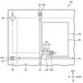
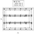
도 1은 본 발명의 일 실시예에 따른 박막 트랜지스터 기판을 포함한 표시 장치를 나타낸 분해 사시도이다.
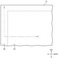
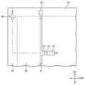
도 2는 도 1의 박막 트랜지스터 기판의 일부를 도시한 평면도이다.
도 3은 도 2의 I-I’선에 따른 단면도이다.
도 4a, 도 5a, 도 6a, 도 7a, 도 8a, 도 9a, 도 10a, 및 도 11a는 도 2 및 도 3에 도시된 박막 트랜지스터 기판의 제조 공정을 순차적으로 도시한 평면도들이다.
도 4b, 도 5b 내지 도 5e, 도 6b, 도 7b 도 8b, 도 9b, 도 10b, 및 도 11b는 도 2 및 도 3에 도시된 박막 트랜지스터 기판의 제조 공정을 순차적으로 도시한 단면도로서, 도 4a, 도 5a, 도 6a, 도 7a, 도 8a, 도 9a, 도 10a, 및 도 11a의 I-I’선에 따른 단면도들이다.
도 12a는 비교예의 박막 트랜지스터 기판의 36개의 측정 위치에서 열처리 공정 전후의 수축 정도를 측정한 값이고, 도 12b는 도 12a에서 36개의 측정 위치에서 열처리 공정 전후의 수축 정도를 도시한 도면이고, 도 12c는 도 12a에서 36개의 측정 위치에서 열처리 공정 전후와 기준 위치의 편차를 도시한 도면이다.1 is an exploded perspective view illustrating a display device including a thin film transistor substrate according to an exemplary embodiment of the present invention.
2 is a plan view showing a part of the thin film transistor substrate of FIG. 1.
3 is a cross-sectional view taken along line II′ of FIG. 2.
4A, 5A, 6A, 7A, 8A, 9A, 10A, and 11A are plan views sequentially illustrating a manufacturing process of the thin film transistor substrate shown in FIGS. 2 and 3.
4B, 5B to 5E, 6B, 7B, 8B, 9B, 10B, and 11B are cross-sectional views sequentially illustrating a manufacturing process of the thin film transistor substrate shown in FIGS. 2 and 3, and FIG. 4A, 5A, 6A, 7A, 8A, 9A, 10A, and 11A are cross-sectional views taken along line I-I' of FIGS.
12A is a value obtained by measuring the degree of shrinkage before and after the heat treatment process at 36 measurement locations of the thin film transistor substrate of the comparative example, and FIG. 12B is a view showing the degree of shrinkage before and after the heat treatment process at 36 measurement locations in FIG. 12A. 12C is a view showing a deviation between a reference position and before and after a heat treatment process at 36 measurement positions in FIG. 12A.
본 발명은 다양한 변경을 가할 수 있고 여러 가지 형태를 가질 수 있는 바, 특정 실시예들을 도면에 예시하고 본문에 상세하게 설명하고자 한다. 그러나, 이는 본 발명을 특정한 개시 형태에 대해 한정하려는 것이 아니며, 본 발명의 사상 및 기술 범위에 포함되는 모든 변경, 균등물 내지 대체물을 포함하는 것으로 이해되어야 한다.In the present invention, various modifications may be made and various forms may be applied, and specific embodiments will be illustrated in the drawings and described in detail in the text. However, this is not intended to limit the present invention to a specific form disclosed, it should be understood to include all changes, equivalents, and substitutes included in the spirit and scope of the present invention.
도 1은 본 발명의 일 실시예에 따른 박막 트랜지스터 기판을 포함한 표시 장치를 나타낸 분해 사시도이다.1 is an exploded perspective view illustrating a display device including a thin film transistor substrate according to an exemplary embodiment of the present invention.
도 1을 참조하면, 상기 표시 장치(1000)는 박막 트랜지스터 기판(100), 대향 기판(200), 및 상기 박막 트랜지스터 기판(100)과 상기 대향 기판(200) 사이에 배치된 액정층(LC)을 포함한다.Referring to FIG. 1, the
상기 박막 트랜지스터 기판(100)은 표시 영역(DA)과 비표시 영역(NA)을 포함한다. 상기 표시 영역(DA)은 복수의 화소 영역들(PX)을 포함한다. 상기 화소 영역들(PX) 각각에는 화소가 구비되고, 상기 화소에서는 영상이 표시된다. 상기 표시 영역(DA)의 전 영역에서 영상이 표시되는 것은 아니고, 후술할 데이터 라인, 게이트 라인, 및 박막트랜지스터와 중첩된 영역에서는 영상이 표시되지 않을 수 있다. 상기 비표시 영역(NA)은 상기 화소 영역(DA)의 주변에 배치되고, 영상이 표시되지 않는다.The thin
상기 박막 트랜지스터 기판(100)은 각 화소 영역(PX)에 구비된 박막 트랜지스터 및 화소 전극을 포함한다. 상기 대향 기판(200)은 공통 전극을 포함할 수 있다.The thin
한편, 이에 제한되는 것은 아니고, 상기 박막 트랜지스터 기판(100)은 박막 트랜지스터, 화소 전극, 및 공통 전극을 포함할 수 있다.Meanwhile, the present invention is not limited thereto, and the thin
상기 액정층(LC)은 유전율 이방성을 가지는 복수의 액정 분자들을 포함한다. 상기 액정층(LC)의 상기 액정 분자들은 상기 화소 전극과 상기 공통 전극 사이에 전계가 인가되면 상기 박막 트랜지스터 기판(100)과 상기 대향 기판(1000) 사이에서 특정 방향으로 회전하며, 이에 따라 상기 액정층(LC)으로 입사되는 광의 투과도를 조절한다.The liquid crystal layer LC includes a plurality of liquid crystal molecules having dielectric anisotropy. The liquid crystal molecules of the liquid crystal layer LC rotate in a specific direction between the thin
도 2는 도 1의 박막 트랜지스터 기판(100)의 일부를 도시한 평면도이고, 도 3은 도 2의 I-I’선에 따른 단면도이다.2 is a plan view illustrating a part of the thin
도 1 내지 도 3을 참조하면, 상기 박막 트랜지스터 기판(100)은 절연 기판(110), 데이터 라인(DL), 게이트 라인(GL), 박막 트랜지스터(TR), 화소 전극(PE), 얼라인 마크(AM), 게이트 패드(GP), 및 데이터 패드(DP)를 포함할 수 있다.1 to 3, the thin
상기 절연 기판(110)은 투명한 유리 또는 플라스틱으로 형성될 수 있다.The
상기 데이터 라인(DL)은 상기 절연 기판(110) 상에 제1 방향(DR1)으로 연장된다. 상기 게이트 라인(GL)은 상기 제1 방향(DR1)과 교차하는 제2 방향(DR2)으로 연장된다. 상기 데이터 라인(DL) 및 상기 게이트 라인(GL)은 서로 교차하고 절연될 수 있다.The data line DL extends in a first direction DR1 on the
도 2에는 하나의 데이터 라인(DL) 및 하나의 게이트 라인(GL)을 일 예로 도시하였으나, 상기 데이터 라인(DL) 및 상기 게이트 라인(GL)은 각각 복수개로 구비될 수 있고, 복수개의 데이터 라인들(DL) 및 복수개의 게이트 라인(GL)은 화소 영역(PX)을 정의한다.In FIG. 2, one data line DL and one gate line GL are illustrated as an example, but the data line DL and the gate line GL may be provided in plurality, respectively, and a plurality of data lines The fields DL and the plurality of gate lines GL define a pixel area PX.
상기 박막 트랜지스터(TR)는 소스 전극(121), 드레인 전극(123), 활성층(125), 및 게이트 전극(130)을 포함할 수 있다.The thin film transistor TR may include a
상기 산화물 반도체 패턴(125)은 상기 절연 기판(110) 상에 형성된다. 상기 산화물 반도체 패턴(125)은 상기 게이트 전극(130)과 중첩하고, 상기 소스 전극(121) 및 상기 드레인 전극(123)에 전기적으로 연결된다.The
상기 산화물 반도체 패턴(125)은 아연(Zn), 인듐(In), 주석(Sn), 갈륨(Ga) 중 적어도 하나를 포함한다. 구체적으로, 상기 산화물 반도체 패턴(125)은 인듐-갈륨-아연 산화물(IGZO)일 수 있다.The
상기 소스 전극(121)은 상기 데이터 라인(DL)으로부터 돌출되어 형성된다. 상기 드레인 전극(123)은 상기 소스 전극(121)과 이격되어 형성된다.The
상기 소스 전극(121) 및 드레인 전극(123) 각각은 배리어층(121b, 123b), 주배선층(121c, 123c), 및 캐핑층(121d, 123d)을 포함할 수 있다. 즉, 상기 소스 전극(121) 및 상기 드레인 전극(123) 각각은 삼중막으로 형성될 수 있다.Each of the
상기 배리어층(121b, 123b) 및 상기 캐핑층(121d, 123d) 각각은 바나듐(V), 지르코늄(Zr), 탄탈륨(Ta), 망간(Mn), 마그네슘(Mg), 크롬(Cr), 몰리브덴(Mo), 코발트(Co), 니오븀(Nb), 및 니켈(Ni) 중 적어도 하나와 구리의 합금 또는 인듐-아연 산화물, 갈륨-아연 산화물 및 알루미늄-아연 산화물 중 적어도 하나의 금속 산화물로 형성할 수 있다. 상기 주배선층(121c, 123c)은 금속으로 이루어질 수 있고, 예를 들어 구리(Cu) 또는 구리 합금으로 이루어질 수 있다.Each of the barrier layers 121b and 123b and the capping layers 121d and 123d is vanadium (V), zirconium (Zr), tantalum (Ta), manganese (Mn), magnesium (Mg), chromium (Cr), molybdenum (Mo), cobalt (Co), niobium (Nb), and nickel (Ni) alloy of at least one of copper or indium-zinc oxide, gallium-zinc oxide, and at least one metal oxide of aluminum-zinc oxide I can. The main wiring layers 121c and 123c may be formed of a metal, for example, copper (Cu) or a copper alloy.
상기 배리어층(121b, 123b)은 상기 주배선층(121c, 123c)을 이루는 구리 등의 물질이 상기 산화물 반도체 패턴(125)으로 확산되는 것을 방지할 수 있다. 상기 캐핑층(121d, 123d)은 상기 주배선층(121c, 123c)을 이루는 금속의 변성에 의해 박막 트랜지스터의 특성에 영향을 미치는 것을 방지할 수 있다.The barrier layers 121b and 123b may prevent a material such as copper forming the main wiring layers 121c and 123c from diffusing into the
한편, 이에 제한되는 것은 아니고, 상기 소스 전극(121) 및 상기 드레인 전극(123) 각각은 캐핑층(121d, 123d)을 제외하고, 배리어층(121b, 123b) 및 주배선층(121c, 123c)의 이중막으로 형성될 수 있고, 상기 배리어층(121b, 123b)을 제외하고, 주배선층(121c, 123c) 및 캐핑층(121d, 123d)의 이중막으로 형성될 수 있다.Meanwhile, the present invention is not limited thereto, and each of the
상기 박막 트랜지스터 기판(100)은 상기 소스 전극(121) 및 상기 드레인 전극(123) 상에 형성된 제1 절연막(127)을 더 포함한다. 상기 제1 절연막(127)은 실리콘 산화물(SiOx) 또는 실리콘 질화물(SiNx)과 같은 절연 물질로 이루어질 수 있다. 상기 제1 절연막(127)은 상기 소스 전극(121) 및 상기 드레인 전극(123)을 상기 게이트 전극(130)과 절연시킬 수 있다.The thin
상기 게이트 전극(130)은 상기 게이트 라인(GL)으로부터 돌출되어 형성된다. 상기 게이트 전극(130)은 상기 제1 절연막(127) 상에 상기 산화물 반도체 패턴(125)과 중첩하게 배치된다.The
상기 게이트 전극(130) 및 상기 게이트 라인(GL) 각각은 단일막 또는 다중막으로 이루어질 수 있다. 상기 게이트 전극(130) 및 상기 게이트 라인(GL) 각각은 알루미늄(Al)과 알루미늄 합금 등 알루미늄 계열의 금속, 은(Ag)과 은 합금 등 은 계열의 금속, 구리(Cu)와 구리 합금 등 구리 계열의 금속, 몰리브덴(Mo)과 몰리브덴 합금 등 몰리브덴 계열의 금속, 크롬(Cr), 티타늄(Ti), 탄탈늄(Ta), 및 망간(Mn)으로 이루어진 적어도 1 이상의 층을 포함할 수 있다.Each of the
상기 제1 절연막(127) 및 상기 게이트 전극(130) 상에 제2 절연막(132)이 형성될 수 있다. 상기 제2 절연막(132)은 실리콘 산화물(SiOx) 또는 실리콘 질화물(SiNx)과 같은 절연 물질로 이루어질 수 있다. 상기 제2 절연막(132)은 상기 게이트 전극(130)과 상기 화소 전극(PE)을 절연시킬 수 있다.A second insulating
상기 박막 트랜지스터 기판(100)은 상기 제1 절연막(127)과 상기 제2 절연막(132) 사이에 배치된 컬러 필터(135)를 더 포함할 수 있다. 상기 컬러 필터(135)는 상기 게이트 전극(130) 및 상기 제1 절연막(127) 상에 배치될 수 있다. 상기 컬러 필터(135)는 상기 화소 영역(PX)에 대응하게 형성되어 상기 화소 영역(PX)을 통과한 광에 색을 제공할 수 있다. 도시하지는 않았으나, 상기 컬러 필터(135)는 적색 컬러 필터, 녹색 컬러 필터, 및 청색 컬러 필터를 포함할 수 있다.The thin
상기 제1 절연막(127) 및 상기 제2 절연막(132)에는 상기 드레인 전극(123)의 상면 일부를 노출하는 제1 콘택홀(CH1)이 구비될 수 있다.A first contact hole CH1 exposing a portion of an upper surface of the
상기 화소 전극(PE)은 상기 제1 콘택홀(CH1)에 대응하게 형성되고, 상기 제1 절연막(127) 및 상기 제2 절연막(132) 상에 형성된다. 상기 화소 전극(PE)은 상기 제1 콘택홀(CH1)을 통해 상기 드레인 전극(123)에 전기적으로 연결된다. 상기 화소 전극(PE)은 상기 드레인 전극(123)을 통해 데이터 전압을 수신한다.The pixel electrode PE is formed to correspond to the first contact hole CH1 and is formed on the first insulating
상기 화소 전극(PE)은 투명 전극일 수 있고, ITO, IZO를 포함할 수 있다.The pixel electrode PE may be a transparent electrode and may include ITO and IZO.
상기 얼라인 마크(AM)는 상기 비표시 영역(NA)에 중첩하게 형성될 수 있다. 상기 얼라인 마크(AM)는 제1 층(137a) 및 마크층(137b, 137c, 138d)을 포함할 수 있다. 상기 제1 층(137a)은 상기 산화물 반도체 패턴(125)과 동일한 층상에 동일한 물질로 형성될 수 있다.The alignment mark AM may be formed to overlap the non-display area NA. The alignment mark AM may include a
상기 마크층(137b, 137c, 138d)은 제2 내지 제4 층들(137b, 137c, 137d)을 포함할 수 있다. 상기 제2 층(137b)은 상기 제1 층(137a) 상에 배치될 수 있다. 상기 제2 층(137b)은 상기 배리어층(121b, 123b)과 동일한 층상에 동일한 물질로 형성될 수 있다. 상기 제2 층(137c)은 상기 제2 층(137b) 상에 배치될 수 있다. 상기 제3 층(137c)은 상기 주배선층(121c, 123c)과 동일한 층상에 동일한 물질로 형성될 수 있다. 상기 제4 층(137d)은 상기 제3 층(137d) 상에 배치될 수 있다. 상기 제4 층(137d)은 상기 캐핑층(121d, 123d)과 동일한 층상에 동일한 물질로 형성될 수 있다.The mark layers 137b, 137c, and 138d may include second to
만일, 상기 소스 전극(121) 및 상기 드레인 전극(123)에서 상기 배리어층(121b, 123b) 및 상기 캐핑층(121d, 123d) 중 어느 하나가 제외된 경우, 상기 얼라인 마크(AM)의 상기 제2 층(137b) 및 상기 제4 층(137d) 중 대응되는 어느 하나가 제외될 수 있다.If any one of the barrier layers 121b and 123b and the capping layers 121d and 123d is excluded from the
상기 게이트 패드(GP)는 상기 게이트 라인(GL)의 일단에 상기 비표시 영역(NA)에 중첩하게 형성될 수 있다. 상기 게이트 패드(GP)는 상기 게이트 라인(GL) 및 상기 게이트 전극(130)과 동일한 층상에 배치된다. 상기 게이트 패드(GP)는 게이트 신호를 수신하여 상기 게이트 라인(GL) 및 상기 게이트 전극(130)에 상기 게이트 신호를 제공할 수 있다. 상기 제2 절연막(132)에는 상기 게이트 패드(GP)의 상면 일부를 노출하는 제2 콘택홀(CH2)이 구비될 수 있다.The gate pad GP may be formed at one end of the gate line GL to overlap the non-display area NA. The gate pad GP is disposed on the same layer as the gate line GL and the
상기 데이터 패드(DP)는 상기 데이터 라인(DL)의 일단에 상기 비표시 영역(NA)에 중첩하게 형성될 수 있다. 상기 데이터 패드(DP)는 상기 데이터 라인(DL), 상기 소스 전극(121), 및 상기 드레인 전극(123)과 동일한 층 상에 배치된다. 상기 데이터 패드(DP)는 데이터 전압을 수신하여 상기 데이터 라인(DL) 및 상기 소스 전극(121)에 상기 데이터 전압을 제공할 수 있다. 상기 제1 절연막(127) 및 상기 제2 절연막(132)에는 상기 데이터 패드(DP)의 상면 일부를 노출하는 제3 콘택홀(CH3)이 구비될 수 있다.The data pad DP may be formed to overlap the non-display area NA at one end of the data line DL. The data pad DP is disposed on the same layer as the data line DL, the
본 발명의 일 실시예에 따른 표시 장치(1000)에 있어서, 상기 얼라인 마크(AM)는 상기 제1 내지 제4 층(137a, 137b, 137c, 137d)을 포함하고, 상기 제2 내지 제4 층(137b, 137c, 137d)은 상기 산화물 반도체 패턴(125)과 동일한 층 상에 배치된 상기 제1 층(137d) 상에 배치된다. 따라서, 상기 얼라인 마크(AM)는 상기 산화물 반도체 패턴(125)이 열처리 공정을 거친후 형성되므로, 열처리 공정으로 인한 수축이 발생되지 않는다. 따라서, 박막 트랜지스터 기판(100)과 대향 기판(200) 사이에 미스얼라인이 발생하는 문제를 방지할 수 있다.In the
도 4a, 도 5a, 도 6a, 도 7a, 도 8a, 도 9a, 도 10a, 및 도 11a는 도 2 및 도 3에 도시된 박막 트랜지스터 기판의 제조 공정을 순차적으로 도시한 평면도들이다.4A, 5A, 6A, 7A, 8A, 9A, 10A, and 11A are plan views sequentially illustrating a manufacturing process of the thin film transistor substrate shown in FIGS. 2 and 3.
도 4b, 도 5b 내지 도 5e, 도 6b, 도 7b 도 8b, 도 9b, 도 10b, 및 도 11b는 도 2 및 도 3에 도시된 박막 트랜지스터 기판의 제조 공정을 순차적으로 도시한 단면도로서, 도 4a, 도 5a, 도 6a, 도 7a, 도 8a, 도 9a, 도 10a, 및 도 11a의 I-I’선에 따른 단면도들이다.4B, 5B to 5E, 6B, 7B, 8B, 9B, 10B, and 11B are cross-sectional views sequentially illustrating a manufacturing process of the thin film transistor substrate shown in FIGS. 2 and 3, and FIG. 4A, 5A, 6A, 7A, 8A, 9A, 10A, and 11A are cross-sectional views taken along line I-I' of FIGS.
도 4a 및 도 4b를 참조하면, 투명한 유리 또는 플라스틱으로 절연 기판(110) 상에 산화물 반도체층(10)을 증착하여 형성한다. 상기 산화물 반도체층(10)은 아연(Zn), 인듐(In), 주석(Sn), 갈륨(Ga) 중 적어도 하나를 포함한다. 구체적으로, 상기 산화물 반도체층(10)은 인듐-갈륨-아연 산화물(IGZO)일 수 있다. 상기 절연 기판(110)은 표시 영역(DA)과 비표시 영역(NA)을 포함할 수 있다.4A and 4B, an
이후, 열처리 공정을 수행한다.Then, a heat treatment process is performed.
열처리 공정은 350℃ 이상의 고온에서 1 시간 이상 진행될 수 있다. 상기 열처리 공정을 통해 상기 산화물 반도체층(10)의 반도체 특성이 향상되어 상기 산화물 반도체층(10)의 일부가 후술할 박막 트랜지스터의 채널로서 역할을 할 수 있다.The heat treatment process may be performed at a high temperature of 350°C or higher for 1 hour or more. Through the heat treatment process, semiconductor properties of the
열처리 공정에 의해 상기 절연 기판(110)에는 수축이 발생될 수 있다. 상기 산화물 반도체층(10) 및 상기 제1 물질층(11)은 상기 절연 기판(110) 상에 전면적으로 형성되고, 패턴이 형성되기 전이므로, 상기 절연 기판(110)에 수축이 발생하더라도 이후 형성될 패턴의 형상에는 영향이 없다.Shrinkage may occur in the insulating
도 5a 및 도 5b를 참조하면, 상기 산화물 반도체층(10) 상에 제1 물질층(11), 제2 물질층(12) 및 제3 물질층(13)을 증착하여 형성한다. 상기 제1 물질층(11) 및 상기 제3 물질층(13) 각각은 바나듐(V), 지르코늄(Zr), 탄탈륨(Ta), 망간(Mn), 마그네슘(Mg), 크롬(Cr), 몰리브덴(Mo), 코발트(Co), 니오븀(Nb), 및 니켈(Ni) 중 적어도 하나와 구리의 합금 또는 인듐-아연 산화물, 갈륨-아연 산화물 및 알루미늄-아연 산화물 중 적어도 하나의 금속 산화물로 형성할 수 있다. 상기 제2 물질층(12)은 금속으로 이루어질 수 있고, 예를 들어 구리(Cu) 또는 구리 합금으로 이루어질 수 있다.5A and 5B, a first material layer 11, a
이후, 도 5c를 참조하면, 상기 제3 물질층(13) 상에 감광성 물질로 이루어진 감광막(50)을 형성한다. 이후, 마스크(MSK)를 통해 상기 감광막(50)에 광을 조사한다. 상기 마스크(MSK)는 하프톤 마스크로서, 조사된 광을 모두 차단시키는 제1 영역(R1), 광의 일부만 투과시키고 일부는 차단하는 제2 영역(R2), 및 조사된 광을 모두 투과시키는 제3 영역(R3)이 마련되어 있으며, 상기 마스크(MSK)를 투과한 광만이 상기 감광막(50)에 조사된다.Thereafter, referring to FIG. 5C, a photosensitive film 50 made of a photosensitive material is formed on the
상기 마스크(MSK)를 통해 노광된 감광막(50)을 현상하면, 도 5d에 도시된 바와 같이 상기 제1 영역(R1)에 대응하는 제1 감광막(51) 및 상기 제2 영역(R2)에 대응하는 제2 감광막(52)이 형성되고, 상기 제3 영역(R3)에 대응되는 감광막(50)의 일부는 완전히 제거되어 상기 절연 기판(110)의 상면이 노출된다.When the photosensitive film 50 exposed through the mask MSK is developed, as shown in FIG. 5D, the first photosensitive film 51 and the second region R2 correspond to the first region R1. The second photoresist layer 52 is formed, and a part of the photosensitive layer 50 corresponding to the third region R3 is completely removed to expose the upper surface of the insulating
상기 제2 영역(R2)은 상기 제1 영역(R1) 보다 노광량이 많기 때문에 상기 제2 감광막(52)은 상기 제1 감광막(51) 보다 작은 두께를 갖는다.Since the exposure amount of the second region R2 is greater than that of the first region R1, the second photoresist film 52 has a thickness smaller than that of the first photoresist film 51.
다만, 본 발명의 일 실시예에서는 상기한 바와 같이 노광된 부분의 상기 감광막(50)이 제거되도록 포지티브 포토레지스트를 사용하였으나, 이에 한정되는 것은 아니며, 본 발명의 다른 실시예에서는 노광되지 않은 부분의 상기 감광막(50)이 제거되도록 하는 네거티브 포토레지스트를 사용할 수도 있다.However, in an embodiment of the present invention, a positive photoresist is used to remove the photosensitive film 50 in the exposed portion as described above, but the present invention is not limited thereto, and in another embodiment of the present invention, A negative photoresist for removing the photoresist layer 50 may be used.
상기 제1 감광막(51) 및 상기 제2 감광막(52)을 마스크로 하여, 상기 제1 감광막(51) 및 상기 제2 감광막(52)에 의해 커버되지 않는 산화물 반도체층(10) 및 제1 내지 제3 물질층(11, 12, 13)을 제1 식각액을 사용하여 선택적으로 제거한다. 이때 상기 제1 식각액은 산화물 반도체층(10) 및 제1 내지 제3 물질층(11, 12, 13)을 모두 식각할 수 있는 물질을 사용할 수 있다. 이에 따라 얼라인 마크(AM) 및 데이터 패턴(DTP)이 형성된다. 상기 얼라인 마크(AM)는 패턴된 산화물 반도체층(10-1) 및 패턴된 제1 내지 제3 물질층(11-1, 12-1, 13-1)을 포함할 수 있다. 또한, 상기 데이터 패턴(DTP)은 패턴된 산화물 반도체층(10-2) 및 패턴된 제1 내지 제3 물질층(11-2, 12-2, 13-2)을 포함할 수 있다.Using the first photosensitive film 51 and the second photosensitive film 52 as masks, the
상기 얼라인 마크(AM)는 상기 제1 감광막(51)에 의해 커버되고, 상기 데이터 패턴(DTP)은 상기 제1 감광막(51) 및 상기 제2 감광막(52)에 의해 커버된다. 상기 제2 감광막(52)에 커버되는 상기 데이터 패턴(DTP)의 일부 영역은 이후 형성될 박막 트랜지스터의 채널에 해당하는 영역일 수 있다.The alignment mark AM is covered by the first photoresist layer 51, and the data pattern DTP is covered by the first photoresist layer 51 and the second photoresist layer 52. A partial region of the data pattern DTP covered by the second photoresist layer 52 may be a region corresponding to a channel of a thin film transistor to be formed later.
이후, 상기 제1 감광막(51)의 일부 및 상기 제2 감광막(52)을 애싱(ashing) 공정 또는 에치 백(etch back) 공정을 통해 제거하게 되면, 도 5e에 도시된 바와 같이, 상기 제2 감광막(52)이 완전히 제거되어 상기 데이터 패턴(DTP)의 상면 일부는 외부에 노출된다. 이때, 상기 제1 감광막(51)은 일부가 제거되어 제3 감광막(53)을 형성한다.Thereafter, when a part of the first photoresist layer 51 and the second photoresist layer 52 are removed through an ashing process or an etch back process, as shown in FIG. 5E, the second Since the photoresist layer 52 is completely removed, a part of the upper surface of the data pattern DTP is exposed to the outside. At this time, a part of the first photoresist film 51 is removed to form a
상기 제3 감광막(53)을 마스크로 하여 상기 제3 감광막(53)에 의해 커버되지 않는 상기 데이터 패턴(DTP)의 일부를 제2 식각액을 사용하여 선택적으로 제거한다. 구체적으로, 상기 데이터 패턴(DTP)의 제1 내지 제3 물질층(11, 12, 13)을 선택적으로 식각하고, 산화물 반도체층(10)을 식각하지 않는다. 상기 제2 식각액은 상기 제1 식각액과 서로 다른 물질일 수 있다. 상기 제2 식각액은 상기 제1 내지 제3 물질층(11, 12, 13)을 식각할 수 있고, 상기 산화물 반도체층(10)을 식각하지 않는 물질일 수 있다.Using the
이후, 상기 제3 감광막(53)을 제거한다.Thereafter, the
도 6a 및 도 6b를 참조하면, 소스 전극(121), 드레인 전극(123), 데이터 라인(DL), 산화물 반도체 패턴(125), 및 데이터 패드(DP)가 형성된다. 이때, 상기 얼라인 마크(AM) 및 상기 데이터 패드(DP)는 상기 비표시 영역(NA)에 중첩하게 형성될 수 있다.6A and 6B, a
상기 소스 전극(121) 및 드레인 전극(123) 각각은 배리어층(121b, 123b), 주배선층(121c, 123c), 및 캐핑층(121d, 123d)을 포함할 수 있다. 즉, 상기 소스 전극(121) 및 상기 드레인 전극(123) 각각은 삼중막으로 형성될 수 있다.Each of the
이후, 도 7a 및 도 7b를 참조하면, 상기 얼라인 마크(AM), 상기 소스 전극(121), 상기 드레인 전극(123), 상기 산화물 반도체 패턴(125), 및 상기 데이터 패드(DP) 상에 제1 절연막(127)을 형성한다.Thereafter, referring to FIGS. 7A and 7B, on the alignment mark AM, the
상기 제1 절연막(127)은 실리콘 산화물(SiOx) 또는 실리콘 질화물(SiNx)과 같은 절연 물질을 증착하여 형성할 수 있다.The first insulating
이후, 도 8a 및 도 8b를 참조하면, 상기 제1 절연막(127) 상에 게이트 전극(130), 게이트 라인(GL), 및 게이트 패드(GP)을 형성한다.Thereafter, referring to FIGS. 8A and 8B, a
상기 게이트 라인(GL)은 상기 데이터 라인(DL)과 교차하게 형성되고, 상기 게이트 전극(130)은 상기 산화물 반도체 패턴(125)에 중첩하게 형성될 수 있다. 상기 게이트 라인(GL), 상기 게이트 전극(130), 및 게이트 패드(GP) 각각은 단일막 또는 다중막으로 형성될 수 있다. 상기 게이트 라인(GL), 상기 게이트 전극(130), 및 게이트 패드(GP) 각각은 알루미늄(Al)과 알루미늄 합금 등 알루미늄 계열의 금속, 은(Ag)과 은 합금 등 은 계열의 금속, 구리(Cu)와 구리 합금 등 구리 계열의 금속, 몰리브덴(Mo)과 몰리브덴 합금 등 몰리브덴 계열의 금속, 크롬(Cr), 티타늄(Ti), 탄탈늄(Ta), 및 망간(Mn)으로 이루어진 적어도 1 이상의 층을 포함할 수 있다.The gate line GL may be formed to cross the data line DL, and the
이후, 도 9a 및 도 9b를 참조하면, 상기 제1 절연막(127) 상에 컬러 필터(135)를 형성할 수 있다. 상기 컬러 필터(135)는 컬러 유기막을 증착한 후, 패터닝하여 형성될 수 있다.Thereafter, referring to FIGS. 9A and 9B, a
이후, 상기 컬러 필터(135) 상에 제2 절연막(132)을 형성할 수 있다. 상기 제2 절연막은 실리콘 산화물(SiOx) 또는 실리콘 질화물(SiNx)과 같은 절연 물질을 증착하여 형성할 수 있다.Thereafter, a second insulating
이후, 도 10a 및 도 10b를 참조하면, 상기 드레인 전극(123)과 중첩하는 상기 제1 절연막(127)의 일부 및 상기 제2 절연막(132)의 일부를 식각하여 제1 콘택홀(CH1)을 형성한다. 또한, 상기 게이트 패드(GP)에 중첩하는 상기 제1 절연막(127)의 일부를 제거하여 제2 콘택홀(CH2)을 형성한다. 또한, 상기 데이터 패드(DP)에 중첩하는 상기 제1 절연막(127)의 일부 및 상기 제2 절연막(132)의 일부를 식각하여 제3 콘택홀(CH3)을 형성한다.Thereafter, referring to FIGS. 10A and 10B, a portion of the first insulating
도 11a 및 도 11b를 참조하면, 상기 제1 콘택홀(CH1)에 의해 노출된 상기 드레인 전극(123)과 전기적으로 연결되도록 화소 전극(PE)을 형성한다. 상기 화소 전극(PE)은 투명 전극일 수 있고, ITO, IZO를 포함할 수 있다.11A and 11B, a pixel electrode PE is formed to be electrically connected to the
이로써 박막 트랜지스터 기판(100)이 완성될 수 있다.Thus, the thin
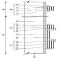
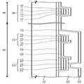
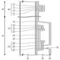
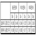
도 12a는 비교예의 박막 트랜지스터 기판의 36개의 측정 위치에서 열처리 공정 전후의 수축 정도를 측정한 값이고, 도 12b는 도 12a에서 36개의 측정 위치에서 열처리 공정 전후의 수축 정도를 도시한 도면이고, 도 12c는 도 12a에서 36개의 측정 위치에서 열처리 공정 전후와 기준 위치의 편차를 도시한 도면이다.12A is a value obtained by measuring the degree of shrinkage before and after the heat treatment process at 36 measurement locations of the thin film transistor substrate of the comparative example, and FIG. 12B is a view showing the degree of shrinkage before and after the heat treatment process at 36 measurement locations in FIG. 12A. 12C is a view showing a deviation between a reference position and before and after a heat treatment process at 36 measurement positions in FIG. 12A.
도 12a 내지 도 12c에서 측정 대상이 된 박막 트랜지스터 기판은 Dx 축이 장축 방향이고, Dy축이 단축 방향인 직사각 형상을 가진다.The thin film transistor substrate as a measurement object in FIGS. 12A to 12C has a rectangular shape in which a Dx axis is a major axis direction and a Dy axis is a minor axis direction.
도 12b에서 검은색 점은 기준 위치를 나타내고, 도 12c에서 Dx축과 Dy축이 교차하는 점은 기준 위치를 나타낸다.In FIG. 12B, a black dot indicates a reference position, and in FIG. 12C, a point where the Dx axis and the Dy axis intersect indicates the reference position.
도 12a 내지 도 12c를 참조하면, 열처리 공정 전에 비해 열처리 공정 후에 수축이 수축이 현저히 많이 발생한 것을 알 수 있다.Referring to FIGS. 12A to 12C, it can be seen that shrinkage occurs significantly more after the heat treatment process than before the heat treatment process.
본 발명의 일 실시예에 따른 박막 트랜지스터 기판의 제조 방법에 의하면, 산화물 반도체 패턴(125) 형성을 위한 열처리 공정 이후 얼라인 마크(AM)를 형성한다. 열처리 공정으로 인해 절연 기판(110)이 수축되더라도 얼라인 마크(AM)는 후속 공정에서 형성되므로, 절연 기판(110)의 수축에 영향을 받지 않는다. 따라서, 상기 얼라인 마크(AM)가 소스 전극 및 드레인 전극과 동일 단계에서 형성되고, 열처리 공정으로 인한 수축에 영향을 받지 않으므로, 이후 게이트 패턴들(게이트 라인 및 게이트 전극)을 형성하는 공정, 화소 전극을 형성하는 공정, 및 박막 트랜지스터 기판과 대향 기판을 합착하는 공정에서 미스얼라인이 발생하는 문제를 방지할 수 있다.According to the method of manufacturing a thin film transistor substrate according to an exemplary embodiment of the present invention, after a heat treatment process for forming the
한편 본 발명은 기재된 실시예에 한정되는 것이 아니고, 본 발명의 사상 및 범위를 벗어나지 않고 다양하게 수정 및 변형을 할 수 있음은 이 기술 분야에서 통상의 지식을 가진 자에게는 자명하다. 따라서, 그러한 변형예 또는 수정예들은 본 발명의 특허청구범위에 속한다 해야 할 것이다.
Meanwhile, it is obvious to those of ordinary skill in the art that the present invention is not limited to the described embodiments, and that various modifications and variations can be made without departing from the spirit and scope of the present invention. Accordingly, such variations or modifications should be included within the scope of the claims of the present invention.
100: 박막 트랜지스터 기판 110: 절연 기판
121: 소스 전극 123: 드레인 전극
125: 산화물 반도체 패턴 127: 제1 절연막
130: 게이트 전극 132: 제2 절연막
AM: 얼라인 마크 PX: 화소 영역100: thin film transistor substrate 110: insulating substrate
121: source electrode 123: drain electrode
125: oxide semiconductor pattern 127: first insulating film
130: gate electrode 132: second insulating film
AM: Alignment mark PX: Pixel area
Claims (17)
Translated fromKorean상기 산화물 반도체층의 열처리 공정을 수행하는 단계;
상기 열처리 공정을 수행하는 단계 이후에 얼라인 마크, 소스 전극, 드레인 전극, 및 산화물 반도체 패턴을 형성하는 단계;
상기 열처리 공정을 수행하는 단계 이후에 게이트 전극을 형성하는 단계; 및
상기 드레인 전극과 연결된 화소 전극을 형성하는 단계를 포함하는 박막 트랜지스터 기판의 제조 방법.Forming an oxide semiconductor layer on the insulating substrate;
Performing a heat treatment process of the oxide semiconductor layer;
Forming an alignment mark, a source electrode, a drain electrode, and an oxide semiconductor pattern after performing the heat treatment process;
Forming a gate electrode after performing the heat treatment process; And
A method of manufacturing a thin film transistor substrate comprising the step of forming a pixel electrode connected to the drain electrode.
상기 얼라인 마크, 상기 소스 전극, 상기 드레인 전극, 및 상기 산화물 반도체 패턴을 형성하는 단계는,
상기 산화물 반도체층 상에 적어도 2층 이상의 증착막들을 형성하는 단계; 및
하프톤 마스크를 사용하여 상기 증착막들을 패터닝하는 단계를 포함하는 것을 특징으로 하는 박막 트랜지스터 기판의 제조 방법.The method of claim 1,
The forming of the alignment mark, the source electrode, the drain electrode, and the oxide semiconductor pattern,
Forming at least two or more deposited films on the oxide semiconductor layer; And
A method of manufacturing a thin film transistor substrate, comprising the step of patterning the deposited films using a halftone mask.
상기 증착막들을 패터닝하는 단계는,
상기 증착막들 상에 감광막을 형성하는 단계;
상기 하프톤 마스크를 사용하여 상기 감광막을 노광 및 현상하여 서로 다른 두께를 갖는 제1 감광막 및 제2 감광막을 형성하는 단계;
상기 제1 감광막 및 상기 제2 감광막을 마스크로하여 상기 증착막들을 식각하여 얼라인 마크 및 데이터 패턴을 형성하는 단계;
상기 제1 감광막의 일부 및 상기 제2 감광막을 제거하여 제3 감광막을 형성하는 단계; 및
상기 제3 감광막을 마스크로 하여 상기 데이터 패턴의 일부를 제거하는 단계를 포함하는 것을 특징으로 하는 박막 트랜지스터 기판의 제조 방법.The method of claim 2,
Patterning the deposited films,
Forming a photosensitive film on the deposition films;
Exposing and developing the photoresist layer using the halftone mask to form a first photoresist layer and a second photoresist layer having different thicknesses;
Forming alignment marks and data patterns by etching the deposition layers using the first photoresist layer and the second photoresist layer as masks;
Forming a third photoresist layer by removing a portion of the first photoresist layer and the second photoresist layer; And
And removing a part of the data pattern using the third photoresist layer as a mask.
상기 얼라인 마크 및 상기 데이터 패턴을 형성하는 단계는 제1 식각액을 사용하고,
상기 데이터 패턴의 일부를 제거하는 단계는 상기 제1 식각액과 서로 다른 제2 식각액을 사용하는 것을 특징으로 하는 박막 트랜지스터 기판의 제조 방법.The method of claim 3,
In the forming of the alignment mark and the data pattern, a first etchant is used,
The step of removing a part of the data pattern includes using a second etchant different from the first etchant.
상기 증착막들을 형성하는 단계는,
상기 산화물 반도체층 상에 제1 물질층을 형성하는 단계;
상기 제1 물질층 상에 제2 물질층을 형성하는 단계; 및
상기 제2 물질층 상에 제3 물질층을 형성하는 단계를 포함하는 것을 특징으로 하는 박막 트랜지스터 기판의 제조 방법.The method of claim 2,
Forming the deposition films,
Forming a first material layer on the oxide semiconductor layer;
Forming a second material layer on the first material layer; And
And forming a third material layer on the second material layer.
상기 제1 물질층 및 상기 제3 물질층은 각각은 바나듐(V), 지르코늄(Zr), 탄탈륨(Ta), 망간(Mn), 마그네슘(Mg), 크롬(Cr), 몰리브덴(Mo), 코발트(Co), 니오븀(Nb), 및 니켈(Ni) 중 적어도 하나와 구리의 합금 또는 인듐-아연 산화물, 갈륨-아연 산화물 및 알루미늄-아연 산화물 중 적어도 하나의 금속 산화물을 포함하는 것을 특징으로 하는 박막 트랜지스터 기판의 제조 방법.The method of claim 5,
Each of the first material layer and the third material layer includes vanadium (V), zirconium (Zr), tantalum (Ta), manganese (Mn), magnesium (Mg), chromium (Cr), molybdenum (Mo), and cobalt. A thin film comprising an alloy of copper with at least one of (Co), niobium (Nb), and nickel (Ni) or a metal oxide of at least one of indium-zinc oxide, gallium-zinc oxide, and aluminum-zinc oxide Method of manufacturing a transistor substrate.
상기 제2 물질층은 구리 또는 구리 합금을 포함하는 것을 특징으로 하는 박막 트랜지스터 기판의 제조 방법.The method of claim 5,
The method of manufacturing a thin film transistor substrate, wherein the second material layer includes copper or a copper alloy.
상기 열처리 공정은 350℃ 이상의 온도에서 수행되는 것을 특징으로 하는 박막 트랜지스터 기판의 제조 방법.The method of claim 1,
The heat treatment process is a method of manufacturing a thin film transistor substrate, characterized in that performed at a temperature of 350 ℃ or higher.
상기 절연 기판은 표시 영역 및 상기 표시 영역에 인접한 비표시 영역을 포함하고,
상기 얼라인 마크는 상기 비표시 영역에 중첩하게 형성되는 것을 특징으로 하는 박막 트랜지스터 기판의 제조 방법.The method of claim 1,
The insulating substrate includes a display area and a non-display area adjacent to the display area,
The alignment mark is a method of manufacturing a thin film transistor substrate, characterized in that formed to overlap the non-display area.
상기 산화물 반도체층은 아연(Zn), 인듐(In), 주석(Sn), 갈륨(Ga) 중 적어도 하나를 포함하는 것을 특징으로 하는 박막 트랜지스터 기판의 제조 방법.The method of claim 1,
The oxide semiconductor layer is a method of manufacturing a thin film transistor substrate comprising at least one of zinc (Zn), indium (In), tin (Sn), and gallium (Ga).
상기 표시 영역에 중첩하고, 상기 절연 기판 상에 배치된 산화물 반도체 패턴;
상기 비표시 영역에 중첩하는 얼라인 마크;
상기 산화물 반도체 패턴 상에 배치된 소스 전극;
상기 산화물 반도체 패턴 상에 배치되고, 상기 소스 전극과 이격된 드레인 전극;
상기 산화물 반도체 패턴 상에 배치되고, 상기 소스 전극 및 상기 드레인 전극과 절연된 게이트 전극; 및
상기 드레인 전극에 연결된 화소 전극을 포함하고,
상기 얼라인 마크는,
상기 산화물 반도체 패턴과 동일한 층상에 배치된 제1 층; 및
상기 소스 전극 및 상기 드레인 전극 각각과 동일한 층상에 배치된 마크층을 포함하는 박막 트랜지스터 기판.An insulating substrate including a display area and a non-display area adjacent to the display area;
An oxide semiconductor pattern overlapping the display area and disposed on the insulating substrate;
An alignment mark overlapping the non-display area;
A source electrode disposed on the oxide semiconductor pattern;
A drain electrode disposed on the oxide semiconductor pattern and spaced apart from the source electrode;
A gate electrode disposed on the oxide semiconductor pattern and insulated from the source electrode and the drain electrode; And
A pixel electrode connected to the drain electrode,
The alignment mark,
A first layer disposed on the same layer as the oxide semiconductor pattern; And
A thin film transistor substrate comprising a mark layer disposed on the same layer as each of the source electrode and the drain electrode.
상기 산화물 반도체 패턴은 아연(Zn), 인듐(In), 주석(Sn), 갈륨(Ga) 중 적어도 하나를 포함하는 것을 특징으로 하는 박막 트랜지스터 기판.The method of claim 11,
The oxide semiconductor pattern includes at least one of zinc (Zn), indium (In), tin (Sn), and gallium (Ga).
상기 소스 전극 및 상기 드레인 전극 각각은,
상기 산화물 반도체 패턴 상에 배치된 배리어층;
상기 배리어층 상에 배치된 주배선층; 및
상기 주배선층 상에 배치된 캐핑층을 포함하는 것을 특징으로 하는 박막 트랜지스터 기판.The method of claim 11,
Each of the source electrode and the drain electrode,
A barrier layer disposed on the oxide semiconductor pattern;
A main wiring layer disposed on the barrier layer; And
A thin film transistor substrate comprising a capping layer disposed on the main wiring layer.
상기 마크층은,
상기 제1 층 상에 배치되고, 상기 배리어층과 동일한 물질로 이루어진 제2 층;
상기 제2 층 상에 배치되고, 상기 주배선층과 동일한 물질로 이루어진 제3 층; 및
상기 제3 층 상에 배치되고, 상기 캐핑층과 동일한 물질로 이루어진 제4 층을 포함하는 것을 특징으로 하는 박막 트랜지스터 기판.The method of claim 13,
The mark layer,
A second layer disposed on the first layer and made of the same material as the barrier layer;
A third layer disposed on the second layer and made of the same material as the main wiring layer; And
And a fourth layer disposed on the third layer and made of the same material as the capping layer.
상기 배리어층 및 상기 캐핑층 각각은 바나듐(V), 지르코늄(Zr), 탄탈륨(Ta), 망간(Mn), 마그네슘(Mg), 크롬(Cr), 몰리브덴(Mo), 코발트(Co), 니오븀(Nb), 및 니켈(Ni) 중 적어도 하나와 구리의 합금 또는 인듐-아연 산화물, 갈륨-아연 산화물 및 알루미늄-아연 산화물 중 적어도 하나의 금속 산화물을 포함하는 것을 특징으로 하는 박막 트랜지스터 기판.The method of claim 13,
Each of the barrier layer and the capping layer is vanadium (V), zirconium (Zr), tantalum (Ta), manganese (Mn), magnesium (Mg), chromium (Cr), molybdenum (Mo), cobalt (Co), and niobium. (Nb), and an alloy of at least one of nickel (Ni) and copper, or a metal oxide of at least one of indium-zinc oxide, gallium-zinc oxide, and aluminum-zinc oxide.
상기 주배선층은 구리 또는 구리 합금을 포함하는 것을 특징으로 하는 박막 트랜지스터 기판.The method of claim 13,
The thin film transistor substrate, wherein the main wiring layer comprises copper or a copper alloy.
상기 박막 트랜지스터 기판에 대향하는 대향 기판; 및
상기 박막 트랜지스터 기판과 상기 대향 기판 사이에 배치된 액정층을 포함하고,
상기 박막 트랜지스터 기판은,
표시 영역 및 상기 표시 영역에 인접한 비표시 영역을 포함하는 절연 기판;
상기 표시 영역에 중첩하고, 상기 절연 기판 상에 배치된 산화물 반도체 패턴;
상기 비표시 영역에 중첩하는 얼라인 마크;
상기 산화물 반도체 패턴 상에 배치된 소스 전극;
상기 산화물 반도체 패턴 상에 배치되고, 상기 소스 전극과 이격된 드레인 전극;
상기 산화물 반도체 패턴 상에 배치되고, 상시 소스 전극 및 상기 드레인 전극과 절연된 게이트 전극; 및
상기 드레인 전극에 연결된 화소 전극을 포함하고,
상기 얼라인 마크는,
상기 산화물 반도체 패턴과 동일한 층상에 배치된 제1 층; 및
상기 소스 전극 및 상기 드레인 전극 각각과 동일한 층상에 배치된 마크층을 포함하는 표시 장치.
A thin film transistor substrate;
A counter substrate facing the thin film transistor substrate; And
A liquid crystal layer disposed between the thin film transistor substrate and the counter substrate,
The thin film transistor substrate,
An insulating substrate including a display area and a non-display area adjacent to the display area;
An oxide semiconductor pattern overlapping the display area and disposed on the insulating substrate;
An alignment mark overlapping the non-display area;
A source electrode disposed on the oxide semiconductor pattern;
A drain electrode disposed on the oxide semiconductor pattern and spaced apart from the source electrode;
A gate electrode disposed on the oxide semiconductor pattern and insulated from the source electrode and the drain electrode at all times; And
A pixel electrode connected to the drain electrode,
The alignment mark,
A first layer disposed on the same layer as the oxide semiconductor pattern; And
And a mark layer disposed on the same layer as each of the source electrode and the drain electrode.
Priority Applications (2)
| Application Number | Priority Date | Filing Date | Title |
|---|---|---|---|
| KR1020140004081AKR102164941B1 (en) | 2014-01-13 | 2014-01-13 | Thin film transistor substrate, display apparatus including the same, and manufacturing method of the thin film transistor substrate |
| US14/458,415US9281406B2 (en) | 2014-01-13 | 2014-08-13 | Thin film transistor substrate, display device including the same, and fabricating method of the thin film transistor substrate |
Applications Claiming Priority (1)
| Application Number | Priority Date | Filing Date | Title |
|---|---|---|---|
| KR1020140004081AKR102164941B1 (en) | 2014-01-13 | 2014-01-13 | Thin film transistor substrate, display apparatus including the same, and manufacturing method of the thin film transistor substrate |
Publications (2)
| Publication Number | Publication Date |
|---|---|
| KR20150084254A KR20150084254A (en) | 2015-07-22 |
| KR102164941B1true KR102164941B1 (en) | 2020-10-14 |
Family
ID=53522058
Family Applications (1)
| Application Number | Title | Priority Date | Filing Date |
|---|---|---|---|
| KR1020140004081AActiveKR102164941B1 (en) | 2014-01-13 | 2014-01-13 | Thin film transistor substrate, display apparatus including the same, and manufacturing method of the thin film transistor substrate |
Country Status (2)
| Country | Link |
|---|---|
| US (1) | US9281406B2 (en) |
| KR (1) | KR102164941B1 (en) |
Cited By (1)
| Publication number | Priority date | Publication date | Assignee | Title |
|---|---|---|---|---|
| US12274093B2 (en) | 2021-06-22 | 2025-04-08 | Samsung Display Co., Ltd. | Wiring substrate and display device including the same |
Families Citing this family (6)
| Publication number | Priority date | Publication date | Assignee | Title |
|---|---|---|---|---|
| CN104299961B (en)* | 2014-10-11 | 2017-02-15 | 合肥鑫晟光电科技有限公司 | Array substrate and manufacturing method thereof |
| KR102273052B1 (en)* | 2015-01-26 | 2021-07-06 | 삼성디스플레이 주식회사 | Manufacturing method of display apparatus |
| US9634036B1 (en)* | 2016-03-11 | 2017-04-25 | Shenzhen China Star Optoelectronics Technology Co., Ltd. | Metal oxide thin-film transistor, method of fabricating the same, and array substrate |
| CN108091697A (en)* | 2017-12-11 | 2018-05-29 | 中华映管股份有限公司 | Thin film transistor and method of manufacturing the same |
| CN111199981B (en) | 2018-11-16 | 2023-04-07 | 合肥鑫晟光电科技有限公司 | Array substrate, preparation method thereof and display device |
| KR102774286B1 (en)* | 2019-12-05 | 2025-02-26 | 엘지디스플레이 주식회사 | Thin film transistor array substrate for digital x-ray detector, the digital x-ray detector and manufacturing method thereof |
Citations (1)
| Publication number | Priority date | Publication date | Assignee | Title |
|---|---|---|---|---|
| US20030068836A1 (en) | 2001-10-10 | 2003-04-10 | Mikio Hongo | Laser annealing apparatus, TFT device and annealing method of the same |
Family Cites Families (20)
| Publication number | Priority date | Publication date | Assignee | Title |
|---|---|---|---|---|
| EP0609809B8 (en)* | 1993-02-01 | 2001-11-21 | Canon Kabushiki Kaisha | Liquid crystal display device |
| DE69616621D1 (en)* | 1995-03-22 | 2001-12-13 | Canon Kk | Display device with even temperature distribution over the screen |
| TW520457B (en)* | 1997-09-30 | 2003-02-11 | Toshiba Corp | Display panel and position adjusting method for the display panel |
| KR20030075522A (en)* | 2002-03-19 | 2003-09-26 | 엘지.필립스 엘시디 주식회사 | Liquid Crystal Display Device having aligning mark |
| JP4474108B2 (en)* | 2002-09-02 | 2010-06-02 | 株式会社 日立ディスプレイズ | Display device, manufacturing method thereof, and manufacturing apparatus |
| JP2007310334A (en)* | 2006-05-19 | 2007-11-29 | Mikuni Denshi Kk | Manufacturing method of liquid crystal display device using halftone exposure method |
| KR100889627B1 (en)* | 2007-08-23 | 2009-03-20 | 삼성모바일디스플레이주식회사 | Thin film transistor, manufacturing method thereof, and organic light emitting display device having same |
| KR101033955B1 (en) | 2008-07-10 | 2011-05-11 | 한양대학교 산학협력단 | Manufacturing method of zinc oxide based semiconductor thin film, thin film transistor using same and manufacturing method thereof |
| KR20100084029A (en) | 2009-01-15 | 2010-07-23 | 주성엔지니어링(주) | Method for forming methla oxide layer and method for manufacturing metal oxide semiconductor thin film transistor |
| KR20100135544A (en) | 2009-06-17 | 2010-12-27 | 삼성전자주식회사 | Transistors, manufacturing methods thereof, and electronic devices including the transistors |
| SG168450A1 (en)* | 2009-08-05 | 2011-02-28 | Sony Corp | Thin film transistor |
| KR101692307B1 (en)* | 2010-08-06 | 2017-01-04 | 엘지디스플레이 주식회사 | Method Of Fabricating Array Substrate For Organic Electroluminescent Display Device |
| TWI621184B (en) | 2010-08-16 | 2018-04-11 | 半導體能源研究所股份有限公司 | Semiconductor device manufacturing method |
| KR101779586B1 (en)* | 2010-09-27 | 2017-10-10 | 엘지디스플레이 주식회사 | Method of fabricating display device using flexible plastic substrate |
| US9219159B2 (en) | 2011-03-25 | 2015-12-22 | Semiconductor Energy Laboratory Co., Ltd. | Method for forming oxide semiconductor film and method for manufacturing semiconductor device |
| US8956944B2 (en) | 2011-03-25 | 2015-02-17 | Semiconductor Energy Laboratory Co., Ltd. | Semiconductor device and method for manufacturing the same |
| US8927329B2 (en) | 2011-03-30 | 2015-01-06 | Semiconductor Energy Laboratory Co., Ltd. | Method for manufacturing oxide semiconductor device with improved electronic properties |
| US9496138B2 (en) | 2011-07-08 | 2016-11-15 | Semiconductor Energy Laboratory Co., Ltd. | Method for manufacturing oxide semiconductor film, method for manufacturing semiconductor device, and semiconductor device |
| JP2014224836A (en)* | 2011-09-16 | 2014-12-04 | シャープ株式会社 | Light emitting device, display device, illumination device, and power generating device |
| KR20130126240A (en)* | 2012-05-11 | 2013-11-20 | 삼성디스플레이 주식회사 | Thin film transistor array panel |
- 2014
- 2014-01-13KRKR1020140004081Apatent/KR102164941B1/enactiveActive
- 2014-08-13USUS14/458,415patent/US9281406B2/enactiveActive
Patent Citations (1)
| Publication number | Priority date | Publication date | Assignee | Title |
|---|---|---|---|---|
| US20030068836A1 (en) | 2001-10-10 | 2003-04-10 | Mikio Hongo | Laser annealing apparatus, TFT device and annealing method of the same |
Cited By (1)
| Publication number | Priority date | Publication date | Assignee | Title |
|---|---|---|---|---|
| US12274093B2 (en) | 2021-06-22 | 2025-04-08 | Samsung Display Co., Ltd. | Wiring substrate and display device including the same |
Also Published As
| Publication number | Publication date |
|---|---|
| US20150200304A1 (en) | 2015-07-16 |
| KR20150084254A (en) | 2015-07-22 |
| US9281406B2 (en) | 2016-03-08 |
Similar Documents
| Publication | Publication Date | Title |
|---|---|---|
| KR102164941B1 (en) | Thin film transistor substrate, display apparatus including the same, and manufacturing method of the thin film transistor substrate | |
| CN101908537B (en) | Array substrate for display equipment and method of fabricating the same | |
| KR101325053B1 (en) | Thin film transistor substrate and manufacturing method thereof | |
| CN105097947B (en) | Thin-film transistor array base-plate and its manufacture method | |
| KR101431136B1 (en) | Method of manufacturing thin film transistor substrate | |
| TWI553837B (en) | Method of making a display panel | |
| WO2017166341A1 (en) | Method for manufacturing tft substrate and manufactured tft substrate | |
| KR20090044119A (en) | Thin film transistor substrate and manufacturing method thereof | |
| CN102832254B (en) | A kind of array base palte and manufacture method, display floater | |
| US20150171111A1 (en) | Thin film transistor array panel and method of manufacturing the same | |
| US9786694B2 (en) | Display device and manufacturing method thereof | |
| US9508828B2 (en) | Array substrate and method of fabricating the same | |
| KR102224457B1 (en) | Display device and method of fabricating the same | |
| US8357937B2 (en) | Thin film transistor liquid crystal display device | |
| US20100155730A1 (en) | Thin film transistor display panel and manufacturing method thereof | |
| US7795057B2 (en) | Liquid crystal display device and fabrication method thereof | |
| KR101898205B1 (en) | Array substrate for fringe field switching mode liquid crystal display device and method for fabricating the same | |
| KR20080043969A (en) | TFT array substrate and manufacturing method thereof | |
| US9171864B2 (en) | Display substrate and method of manufacturing the same | |
| KR102090518B1 (en) | Oxide semiconductor thin film transistor and Display Device and Method of manufacturing the sames | |
| CN102751333A (en) | Active element and manufacturing method thereof | |
| CN102854677A (en) | Array substrate, production method of array substrate and display device | |
| US9035364B2 (en) | Active device and fabricating method thereof | |
| KR102035004B1 (en) | Array substrate for liquid crystal display device and method of fabricating the same | |
| CN101207092B (en) | Liquid crystal display device and manufacturing method thereof |
Legal Events
| Date | Code | Title | Description |
|---|---|---|---|
| PA0109 | Patent application | Patent event code:PA01091R01D Comment text:Patent Application Patent event date:20140113 | |
| PG1501 | Laying open of application | ||
| A201 | Request for examination | ||
| PA0201 | Request for examination | Patent event code:PA02012R01D Patent event date:20181213 Comment text:Request for Examination of Application Patent event code:PA02011R01I Patent event date:20140113 Comment text:Patent Application | |
| E902 | Notification of reason for refusal | ||
| PE0902 | Notice of grounds for rejection | Comment text:Notification of reason for refusal Patent event date:20200120 Patent event code:PE09021S01D | |
| E701 | Decision to grant or registration of patent right | ||
| PE0701 | Decision of registration | Patent event code:PE07011S01D Comment text:Decision to Grant Registration Patent event date:20200727 | |
| GRNT | Written decision to grant | ||
| PR0701 | Registration of establishment | Comment text:Registration of Establishment Patent event date:20201006 Patent event code:PR07011E01D | |
| PR1002 | Payment of registration fee | Payment date:20201007 End annual number:3 Start annual number:1 | |
| PG1601 | Publication of registration | ||
| PR1001 | Payment of annual fee | Payment date:20230925 Start annual number:4 End annual number:4 | |
| PR1001 | Payment of annual fee |