KR102164542B1 - Semiconductor Devices Having Buried Gate Structures and Methods of the Same - Google Patents
Semiconductor Devices Having Buried Gate Structures and Methods of the SameDownload PDFInfo
- Publication number
- KR102164542B1 KR102164542B1KR1020140061198AKR20140061198AKR102164542B1KR 102164542 B1KR102164542 B1KR 102164542B1KR 1020140061198 AKR1020140061198 AKR 1020140061198AKR 20140061198 AKR20140061198 AKR 20140061198AKR 102164542 B1KR102164542 B1KR 102164542B1
- Authority
- KR
- South Korea
- Prior art keywords
- gate
- layer
- insulating layer
- bit line
- trench
- Prior art date
- Legal status (The legal status is an assumption and is not a legal conclusion. Google has not performed a legal analysis and makes no representation as to the accuracy of the status listed.)
- Active
Links
Images


Classifications
- H—ELECTRICITY
- H10—SEMICONDUCTOR DEVICES; ELECTRIC SOLID-STATE DEVICES NOT OTHERWISE PROVIDED FOR
- H10B—ELECTRONIC MEMORY DEVICES
- H10B12/00—Dynamic random access memory [DRAM] devices
- H10B12/30—DRAM devices comprising one-transistor - one-capacitor [1T-1C] memory cells
- H10B12/34—DRAM devices comprising one-transistor - one-capacitor [1T-1C] memory cells the transistor being at least partially in a trench in the substrate
- H—ELECTRICITY
- H10—SEMICONDUCTOR DEVICES; ELECTRIC SOLID-STATE DEVICES NOT OTHERWISE PROVIDED FOR
- H10D—INORGANIC ELECTRIC SEMICONDUCTOR DEVICES
- H10D30/00—Field-effect transistors [FET]
- H10D30/60—Insulated-gate field-effect transistors [IGFET]
- H10D30/64—Double-diffused metal-oxide semiconductor [DMOS] FETs
- H10D30/66—Vertical DMOS [VDMOS] FETs
- H10D30/668—Vertical DMOS [VDMOS] FETs having trench gate electrodes, e.g. UMOS transistors
- H—ELECTRICITY
- H10—SEMICONDUCTOR DEVICES; ELECTRIC SOLID-STATE DEVICES NOT OTHERWISE PROVIDED FOR
- H10B—ELECTRONIC MEMORY DEVICES
- H10B12/00—Dynamic random access memory [DRAM] devices
- H10B12/01—Manufacture or treatment
- H10B12/02—Manufacture or treatment for one transistor one-capacitor [1T-1C] memory cells
- H10B12/03—Making the capacitor or connections thereto
- H10B12/033—Making the capacitor or connections thereto the capacitor extending over the transistor
- H10B12/0335—Making a connection between the transistor and the capacitor, e.g. plug
- H—ELECTRICITY
- H10—SEMICONDUCTOR DEVICES; ELECTRIC SOLID-STATE DEVICES NOT OTHERWISE PROVIDED FOR
- H10B—ELECTRONIC MEMORY DEVICES
- H10B12/00—Dynamic random access memory [DRAM] devices
- H10B12/01—Manufacture or treatment
- H10B12/02—Manufacture or treatment for one transistor one-capacitor [1T-1C] memory cells
- H10B12/05—Making the transistor
- H10B12/053—Making the transistor the transistor being at least partially in a trench in the substrate
- H—ELECTRICITY
- H10—SEMICONDUCTOR DEVICES; ELECTRIC SOLID-STATE DEVICES NOT OTHERWISE PROVIDED FOR
- H10B—ELECTRONIC MEMORY DEVICES
- H10B12/00—Dynamic random access memory [DRAM] devices
- H10B12/30—DRAM devices comprising one-transistor - one-capacitor [1T-1C] memory cells
- H10B12/31—DRAM devices comprising one-transistor - one-capacitor [1T-1C] memory cells having a storage electrode stacked over the transistor
- H10B12/315—DRAM devices comprising one-transistor - one-capacitor [1T-1C] memory cells having a storage electrode stacked over the transistor with the capacitor higher than a bit line
- H—ELECTRICITY
- H10—SEMICONDUCTOR DEVICES; ELECTRIC SOLID-STATE DEVICES NOT OTHERWISE PROVIDED FOR
- H10B—ELECTRONIC MEMORY DEVICES
- H10B12/00—Dynamic random access memory [DRAM] devices
- H10B12/30—DRAM devices comprising one-transistor - one-capacitor [1T-1C] memory cells
- H10B12/48—Data lines or contacts therefor
- H10B12/482—Bit lines
- H—ELECTRICITY
- H10—SEMICONDUCTOR DEVICES; ELECTRIC SOLID-STATE DEVICES NOT OTHERWISE PROVIDED FOR
- H10D—INORGANIC ELECTRIC SEMICONDUCTOR DEVICES
- H10D30/00—Field-effect transistors [FET]
- H10D30/60—Insulated-gate field-effect transistors [IGFET]
- H—ELECTRICITY
- H10—SEMICONDUCTOR DEVICES; ELECTRIC SOLID-STATE DEVICES NOT OTHERWISE PROVIDED FOR
- H10D—INORGANIC ELECTRIC SEMICONDUCTOR DEVICES
- H10D30/00—Field-effect transistors [FET]
- H10D30/60—Insulated-gate field-effect transistors [IGFET]
- H10D30/611—Insulated-gate field-effect transistors [IGFET] having multiple independently-addressable gate electrodes influencing the same channel
- H—ELECTRICITY
- H10—SEMICONDUCTOR DEVICES; ELECTRIC SOLID-STATE DEVICES NOT OTHERWISE PROVIDED FOR
- H10D—INORGANIC ELECTRIC SEMICONDUCTOR DEVICES
- H10D30/00—Field-effect transistors [FET]
- H10D30/60—Insulated-gate field-effect transistors [IGFET]
- H10D30/63—Vertical IGFETs
- H—ELECTRICITY
- H10—SEMICONDUCTOR DEVICES; ELECTRIC SOLID-STATE DEVICES NOT OTHERWISE PROVIDED FOR
- H10D—INORGANIC ELECTRIC SEMICONDUCTOR DEVICES
- H10D30/00—Field-effect transistors [FET]
- H10D30/60—Insulated-gate field-effect transistors [IGFET]
- H10D30/64—Double-diffused metal-oxide semiconductor [DMOS] FETs
- H10D30/66—Vertical DMOS [VDMOS] FETs
- H10D30/667—Vertical DMOS [VDMOS] FETs having substrates comprising insulating layers, e.g. SOI-VDMOS transistors
- H—ELECTRICITY
- H10—SEMICONDUCTOR DEVICES; ELECTRIC SOLID-STATE DEVICES NOT OTHERWISE PROVIDED FOR
- H10D—INORGANIC ELECTRIC SEMICONDUCTOR DEVICES
- H10D64/00—Electrodes of devices having potential barriers
- H10D64/20—Electrodes characterised by their shapes, relative sizes or dispositions
- H10D64/27—Electrodes not carrying the current to be rectified, amplified, oscillated or switched, e.g. gates
- H10D64/311—Gate electrodes for field-effect devices
- H10D64/411—Gate electrodes for field-effect devices for FETs
- H10D64/511—Gate electrodes for field-effect devices for FETs for IGFETs
- H10D64/512—Disposition of the gate electrodes, e.g. buried gates
- H10D64/513—Disposition of the gate electrodes, e.g. buried gates within recesses in the substrate, e.g. trench gates, groove gates or buried gates
- H—ELECTRICITY
- H10—SEMICONDUCTOR DEVICES; ELECTRIC SOLID-STATE DEVICES NOT OTHERWISE PROVIDED FOR
- H10D—INORGANIC ELECTRIC SEMICONDUCTOR DEVICES
- H10D64/00—Electrodes of devices having potential barriers
- H10D64/60—Electrodes characterised by their materials
- H10D64/66—Electrodes having a conductor capacitively coupled to a semiconductor by an insulator, e.g. MIS electrodes
- H10D64/667—Electrodes having a conductor capacitively coupled to a semiconductor by an insulator, e.g. MIS electrodes the conductor comprising a layer of alloy material, compound material or organic material contacting the insulator, e.g. TiN workfunction layers
Landscapes
- Engineering & Computer Science (AREA)
- Manufacturing & Machinery (AREA)
- Semiconductor Memories (AREA)
- Chemical & Material Sciences (AREA)
- Composite Materials (AREA)
- Materials Engineering (AREA)
- Internal Circuitry In Semiconductor Integrated Circuit Devices (AREA)
Abstract
Translated fromKoreanDescription
Translated fromKorean본 발명은 매립형 게이트 구조체를 갖는 반도체 소자 및 그 제조 방법에 관한 것이다.The present invention relates to a semiconductor device having a buried gate structure and a method of manufacturing the same.
반도체 소자의 집적도가 점차 증가하면서 기판 내에 매립된 게이트 구조체를 갖는 반도체 소자의 구조가 제안되었다. 매립된 게이트 구조체의 동작 및 신뢰성을 개선하고 안정화시키기 위한 다양한 제안과 연구가 진행되고 있다.As the degree of integration of semiconductor devices gradually increases, a structure of a semiconductor device having a gate structure embedded in a substrate has been proposed. Various proposals and studies are being conducted to improve and stabilize the operation and reliability of the buried gate structure.
본 발명이 해결하고자 하는 과제는 매립형 게이트 구조체를 갖는 반도체 소자를 제공하는 것이다.The problem to be solved by the present invention is to provide a semiconductor device having a buried gate structure.
본 발명이 해결하고자 하는 과제는 게이트 배리어 패턴의 상단이 리세스된 매립형 게이트 구조체를 갖는 반도체 소자를 제공하는 것이다.The problem to be solved by the present invention is to provide a semiconductor device having a buried gate structure in which an upper end of a gate barrier pattern is recessed.
본 발명이 해결하고자 하는 과제는 버퍼 산화층을 갖는 매립형 게이트 구조체를 갖는 반도체 소자를 제공하는 것이다.The problem to be solved by the present invention is to provide a semiconductor device having a buried gate structure having a buffer oxide layer.
본 발명이 해결하고자 하는 과제는 확산 방법을 이용하여 형성된 소스 영역 및 드레인 영역을 갖는 매립형 게이트 구조체를 갖는 반도체 소자를 제공하는 것이다.The problem to be solved by the present invention is to provide a semiconductor device having a buried gate structure having a source region and a drain region formed using a diffusion method.
본 발명이 해결하고자 하는 과제는 기판의 활성 영역에 가해지는 컴프레시브 스트레스를 완화시킬 수 있는 매립형 게이트 구조체를 갖는 반도체 소자를 제공하는 것이다.The problem to be solved by the present invention is to provide a semiconductor device having a buried gate structure capable of alleviating a compressive stress applied to an active region of a substrate.
본 발명이 해결하고자 하는 과제는 매립형 게이트 구조체를 갖는 반도체 소자를 제조하는 방법을 제공하는 것이다.The problem to be solved by the present invention is to provide a method of manufacturing a semiconductor device having a buried gate structure.
본 발명이 해결하고자 하는 과제는 게이트 배리어 패턴의 상단이 리세스된 매립형 게이트 구조체를 갖는 반도체 소자를 제조하는 방법을 제공하는 것이다.The problem to be solved by the present invention is to provide a method of manufacturing a semiconductor device having a buried gate structure in which an upper end of a gate barrier pattern is recessed.
본 발명이 해결하고자 하는 과제는 버퍼 산화층을 갖는 매립형 게이트 구조체를 갖는 반도체 소자를 제조하는 방법을 제공하는 것이다.The problem to be solved by the present invention is to provide a method of manufacturing a semiconductor device having a buried gate structure having a buffer oxide layer.
본 발명이 해결하고자 하는 과제는 확산 방법을 이용하여 형성된 소스 영역 및 드레인 영역을 갖는 매립형 게이트 구조체를 갖는 반도체 소자를 제조하는 방법을 제공하는 것이다.The problem to be solved by the present invention is to provide a method of manufacturing a semiconductor device having a buried gate structure having a source region and a drain region formed using a diffusion method.
본 발명이 해결하고자 하는 과제는 기판의 활성 영역에 가해지는 컴프레시브 스트레스를 완화시킬 수 있는 매립형 게이트 구조체를 갖는 반도체 소자를 제조하는 방법을 제공하는 것이다.An object to be solved by the present invention is to provide a method of manufacturing a semiconductor device having a buried gate structure capable of alleviating a compressive stress applied to an active region of a substrate.
본 발명이 해결하고자 하는 다양한 과제들은 이상에서 언급한 과제들에 제한되지 않으며, 언급되지 않은 또 다른 과제들은 아래의 기재로부터 당 업자에게 명확하게 이해될 수 있을 것이다.Various problems to be solved by the present invention are not limited to the problems mentioned above, and other problems that are not mentioned will be clearly understood by those skilled in the art from the following description.
본 발명의 기술적 사상의 일 실시예에 의한 반도체 소자는 기판 내에 활성 영역을 정의하는 소자 분리 영역, 및 상기 기판 내의 상기 활성 영역 내에 매립된 게이트 구조체들을 포함한다. 상기 게이트 구조체들 중 적어도 하나는 게이트 트렌치, 상기 게이트 트렌치의 내벽 상에 컨포멀하게 형성된 게이트 절연층, 상기 게이트 트렌치의 하부 영역의 상기 게이트 절연층 상에 컨포멀하게 형성된 게이트 배리어 패턴, 상기 게이트 배리어 패턴 상에 형성되고 상기 게이트 트렌치의 하부 영역을 채우는 게이트 전극 패턴, 상기 게이트 배리어 패턴 및 상기 게이트 전극 패턴과 접촉하도록 상기 게이트 트렌치의 상부 영역의 상기 게이트 절연층 상에 컨포멀하게 형성된 전극 보호층, 상기 전극 보호층 상에 컨포멀하게 형성된 버퍼 산화층, 및 상기 게이트 트렌치의 상부 영역을 채우도록 상기 버퍼 산화층 상에 형성된 게이트 캡핑 절연층을 포함할 수 있다.A semiconductor device according to an embodiment of the inventive concept includes an isolation region defining an active region in a substrate, and gate structures buried in the active region in the substrate. At least one of the gate structures includes a gate trench, a gate insulating layer conformally formed on an inner wall of the gate trench, a gate barrier pattern conformally formed on the gate insulating layer in a lower region of the gate trench, and the gate barrier A gate electrode pattern formed on a pattern and filling a lower region of the gate trench, an electrode protective layer conformally formed on the gate insulating layer in an upper region of the gate trench to contact the gate barrier pattern and the gate electrode pattern, A buffer oxide layer conformally formed on the electrode protection layer, and a gate capping insulating layer formed on the buffer oxide layer to fill an upper region of the gate trench.
상기 게이트 절연층은 상기 게이트 트렌치의 상기 내벽 상에 전체적으로 형성될 수 있다.The gate insulating layer may be entirely formed on the inner wall of the gate trench.
상기 전극 보호층은 실리콘 질화물을 포함할 수 있다.The electrode protective layer may include silicon nitride.
상기 버퍼 산화층은 N형 불순물을 가진 실리콘 산화물을 포함할 수 있다.The buffer oxide layer may include silicon oxide having an N-type impurity.
상기 반도체 소자는 상기 게이트 구조체들 사이의 소스 영역을 더 포함 수 있다.The semiconductor device may further include a source region between the gate structures.
상기 소스 영역은 상기 버퍼 산화층이 포함하는 N형 불순물과 동일한 도펀트를 포함할 수 있다.The source region may include the same dopant as the N-type impurity included in the buffer oxide layer.
상기 반도체 소자는 상기 소스 영역과 수직으로 정렬 및 중첩하는 비트 라인 컨택 플러그를 더 포함 수 있다.The semiconductor device may further include a bit line contact plug vertically aligned and overlapped with the source region.
상기 비트 라인 컨택 플러그의 하면의 측부 및 측면의 하부는 상기 게이트 캡핑 절연층, 상기 버퍼 산화층, 및 상기 전극 보호층과 접촉할 수 있다.A side portion of a lower surface of the bit line contact plug and a lower portion of the side surface may contact the gate capping insulating layer, the buffer oxide layer, and the electrode protective layer.
상기 비트 라인 컨택 플러그의 수평 폭은 상기 소스 영역의 수평 폭 보다 넓을 수 있다.The horizontal width of the bit line contact plug may be wider than the horizontal width of the source region.
상기 반도체 소자는 상기 비트 라인 컨택 플러그 상의 비트 라인 구조체를 더 포함할 수 있다.The semiconductor device may further include a bit line structure on the bit line contact plug.
상기 비트 라인 구조체와 수직으로 중첩하지 않고 노출된 상기 비트 라인 컨택 플러그의 상면은 경사질 수 있다.An upper surface of the bit line contact plug exposed without vertically overlapping the bit line structure may be inclined.
상기 반도체 소자는 상기 비트 라인 컨택 플러그의 상기 경사진 상면 상에 형성된 실리콘 산화물 층을 더 포함할 수 있다.The semiconductor device may further include a silicon oxide layer formed on the inclined upper surface of the bit line contact plug.
상기 반도체 소자는 상기 비트 라인 컨택 플러그의 상기 경사진 상면 상에 형성된 실리콘 산화물 층을 더 포함할 수 있다.The semiconductor device may further include a silicon oxide layer formed on the inclined upper surface of the bit line contact plug.
상기 반도체 소자는 상기 비트 라인 구조체를 덮는 스페이서 층을 더 포함할 수 있다.The semiconductor device may further include a spacer layer covering the bit line structure.
상기 스페이서 층은 상기 리세스된 상기 비트 라인 컨택 플러그의 상기 경사진 상면 상에 형성될 수 있다.The spacer layer may be formed on the inclined upper surface of the recessed bit line contact plug.
상기 게이트 캡핑 절연층은 실리콘 질화물을 포함할 수 있다.The gate capping insulating layer may include silicon nitride.
상기 게이트 배리어 패턴의 상단부는 상기 게이트 전극 패턴의 상단부보다 낮게 리세스될 수 있다.The upper end of the gate barrier pattern may be recessed lower than the upper end of the gate electrode pattern.
상기 전극 보호층의 일부는 상기 리세스된 게이트 배리어 패턴의 상단부 상의 상기 게이트 절연층과 상기 게이트 전극 패턴사이에 개재될 수 있다.A portion of the electrode protection layer may be interposed between the gate insulating layer and the gate electrode pattern on an upper end of the recessed gate barrier pattern.
본 발명의 일 실시예에 의한 반도체 소자는 기판 내에 매립된 게이트 구조체들, 상기 게이트 구조체들 사이의 상기 기판과 수직으로 정렬되도록 상기 기판 상에 형성된 비트 라인 컨택 플러그, 상기 비트 라인 컨택 플러그 상에 형성된 비트 라인 구조체, 및 상기 비트 라인 구조체를 덮는 스페이서 층을 포함한다.The semiconductor device according to an embodiment of the present invention includes gate structures buried in a substrate, a bit line contact plug formed on the substrate so as to be vertically aligned with the substrate between the gate structures, and the bit line contact plug formed on the bit line contact plug. And a bit line structure, and a spacer layer covering the bit line structure.
상기 게이트 구조체들은, 각각, 상기 기판 내에 형성된 게이트 트렌치, 상기 게이트 트렌치의 내벽 상에 컨포멀하게 형성된 게이트 절연층, 상기 게이트 트렌치의 하부 영역의 상기 게이트 절연층 상에 컨포멀하게 형성된 게이트 배리어 패턴, 상기 게이트 배리어 패턴 상에 형성되고 상기 게이트 트렌치의 하부 영역을 채우는 게이트 전극 패턴, 상기 게이트 트렌치의 상부 영역의 상기 게이트 절연층 상에 컨포멀하게 형성되는 실리콘 산화물 층, 및 상기 게이트 트렌치의 상부 영역을 채우도록 상기 실리콘 산화물 층 상에 형성된 실리콘 질화물 층을 포함할 수 있다.Each of the gate structures may include a gate trench formed in the substrate, a gate insulating layer conformally formed on an inner wall of the gate trench, a gate barrier pattern conformally formed on the gate insulating layer in a lower region of the gate trench, A gate electrode pattern formed on the gate barrier pattern and filling a lower region of the gate trench, a silicon oxide layer conformally formed on the gate insulating layer in an upper region of the gate trench, and an upper region of the gate trench. It may include a silicon nitride layer formed on the silicon oxide layer to fill.
상기 반도체 소자는 상기 게이트 절연층과 상기 실리콘 산화물 층 사이에 컨포멀하게 형성된 실리콘 질화물 층을 더 포함할 수 있다.The semiconductor device may further include a silicon nitride layer conformally formed between the gate insulating layer and the silicon oxide layer.
상기 게이트 배리어 패턴의 상단부는 상기 게이트 전극 패턴의 상단부보다 낮게 리세스되어 상기 게이트 절연층과 상기 게이트 전극 패턴 사이에 갭이 형성될 수 있다.The upper end of the gate barrier pattern may be recessed lower than the upper end of the gate electrode pattern to form a gap between the gate insulating layer and the gate electrode pattern.
상기 실리콘 산화물 층의 일부는 상기 갭 내에 채워질 수 있다.A part of the silicon oxide layer may be filled in the gap.
상기 실리콘 산화물 층은 인(P)을 포함할 수 있다.The silicon oxide layer may include phosphorus (P).
본 발명의 일 실시예에 의한 반도체 소자는, 기판 내에 활성 영역을 정의하는 소자 분리 영역, 및 상기 기판 내의 상기 활성 영역 내에 매립된 게이트 구조체들, 상기 게이트 구조체들 사이의 상기 활성 영역과 수직으로 정렬되도록 상기 기판 상에 형성된 비트 라인 컨택 플러그, 및 상기 비트 라인 컨택 플러그 상에 형성된 비트 라인 구조체를 포함한다.In the semiconductor device according to an embodiment of the present invention, a device isolation region defining an active region in a substrate, gate structures buried in the active region in the substrate, and vertical alignment with the active region between the gate structures And a bit line contact plug formed on the substrate, and a bit line structure formed on the bit line contact plug.
상기 게이트 구조체들은, 각각, 상기 기판 내에 형성된 게이트 트렌치, 상기 게이트 트렌치의 내벽 상에 컨포멀하게 형성된 게이트 절연층, 상기 게이트 트렌치의 하부 영역의 상기 게이트 절연층 상에 컨포멀하게 형성된 게이트 배리어 패턴, 상기 게이트 배리어 패턴 상에 형성되고 상기 게이트 트렌치의 하부 영역을 채우는 게이트 전극 패턴, 상기 게이트 배리어 패턴 및 상기 게이트 전극 패턴과 접촉하도록 상기 게이트 트렌치의 상부 영역의 상기 게이트 절연층 상에 컨포멀하게 형성된 실리콘 질화물 층, 상기 게이트 트렌치의 상부 영역의 상기 게이트 절연층 상에 컨포멀하게 형성되는 실리콘 산화물 층, 및 상기 게이트 트렌치의 상부 영역을 채우도록 상기 실리콘 산화물 층 상에 형성된 게이트 캡핑 절연층을 포함할 수 있다.Each of the gate structures may include a gate trench formed in the substrate, a gate insulating layer conformally formed on an inner wall of the gate trench, a gate barrier pattern conformally formed on the gate insulating layer in a lower region of the gate trench, A gate electrode pattern formed on the gate barrier pattern and filling a lower region of the gate trench; silicon conformally formed on the gate insulating layer in an upper region of the gate trench to contact the gate barrier pattern and the gate electrode pattern A nitride layer, a silicon oxide layer conformally formed on the gate insulating layer in an upper region of the gate trench, and a gate capping insulating layer formed on the silicon oxide layer to fill an upper region of the gate trench. have.
상기 게이트 배리어 패턴의 상단부는 상기 게이트 전극 패턴의 상단부보다 낮게 리세스될 수 있다.The upper end of the gate barrier pattern may be recessed lower than the upper end of the gate electrode pattern.
상기 비트 라인 컨택 플러그의 하부는 상기 실리콘 질화물 층, 상기 실리콘 산화물 층, 및 상기 게이트 캡핑 절연층과 접촉하도록 상기 기판의 상면 보다 낮게 아래로 돌출할 수 있다.A lower portion of the bit line contact plug may protrude lower than the upper surface of the substrate so as to contact the silicon nitride layer, the silicon oxide layer, and the gate capping insulating layer.
상기 활성 영역은 상기 게이트 구조체들 사이의 소스 영역, 및 상기 소자 분리 영역들과 상기 게이트 구조체들 사이의 드레인 영역들을 포함할 수 있다.The active region may include a source region between the gate structures and drain regions between the device isolation regions and the gate structures.
상기 실리콘 산화물 층, 상기 소스 영역, 및 상기 드레인 영역들은 N형 도펀트들을 포함할 수 있다.The silicon oxide layer, the source region, and the drain regions may include N-type dopants.
기타 실시 예들의 구체적인 사항들은 상세한 설명 및 도면들에 포함되어 있다.Details of other embodiments are included in the detailed description and drawings.
본 발명의 기술적 사상의 다양한 실시예들에 의한 반도체 소자들은 상단부가 게이트 전극 패턴의 상단부보다 낮게 리세스된 게이트 배리어 패턴을 가진 게이트 구조체를 포함할 수 있다. 상기 게이트 배리어 패턴의 상단부가 리세스됨으로써, 상기 게이트 전극 패턴과 소스 영역의 거리 및 상기 게이트 전극 패턴과 드레인 영역들 간의 거리가 증가할 수 있다. 따라서, 상기 게이트 구조체가 턴온(turn on)됨에 따라 발생하는 GIDL(gate induced drain leakage current)가 감소할 수 있다.Semiconductor devices according to various embodiments of the inventive concept may include a gate structure having a gate barrier pattern in which an upper end is recessed lower than an upper end of the gate electrode pattern. As the upper end of the gate barrier pattern is recessed, a distance between the gate electrode pattern and the source region and a distance between the gate electrode pattern and the drain region may increase. Accordingly, the gate induced drain leakage current (GIDL) generated as the gate structure is turned on may be reduced.
본 발명의 기술적 사상의 다양한 실시예들에 의한 반도체 소자들은 실리콘 산화물 층을 가진 게이트 구조체를 포함할 수 있다. 상기 실리콘 산화물 층은 게이트 구조체의 실리콘 질화물 층이 기판의 활성 영역(채널)에 가하는 컴프레시브 스트레스를 완화시킬 수 있다. 따라서, 캐리어(전자)의 이동도가 저하되는 것이 완화될 수 있다.Semiconductor devices according to various embodiments of the inventive concept may include a gate structure having a silicon oxide layer. The silicon oxide layer may relieve a compressive stress applied by the silicon nitride layer of the gate structure to the active region (channel) of the substrate. Therefore, the decrease in the mobility of the carriers (electrons) can be alleviated.
상기 실리콘 산화물 층은 상기 실리콘 질화물 층보다 소프트하고 유연하므로 실리콘과 실리콘 질화물의 열 팽창 계수의 차이에 따른 부(-)적인 현상들이 방지 또는 완화될 수 있다.Since the silicon oxide layer is softer and more flexible than the silicon nitride layer, negative phenomena due to the difference in thermal expansion coefficients of silicon and silicon nitride may be prevented or alleviated.
상기 실리콘 산화물 층은 인(P, phosphorous) 같은 N형 불순물을 포함할 수 있다. 상기 실리콘 산화물 층의 상기 N형 불순물은 확산 공정을 통하여 상기 기판의 상기 활성 영역으로 확산, 이동할 수 있다. 따라서, 상기 활성 영역 내에 물리적 손상이 없는 소스 영역 및 드레인 영역이 형성될 수 있다.The silicon oxide layer may contain N-type impurities such as phosphorous (P). The N-type impurity of the silicon oxide layer may diffuse and migrate to the active region of the substrate through a diffusion process. Accordingly, a source region and a drain region without physical damage may be formed in the active region.
언급되지 않은 본 발명의 다양한 효과들은 본문 내에서 언급될 것이다.Various effects of the present invention not mentioned will be mentioned in the text.
도 1a 및 1b는 본 발명의 실시예들에 의한 반도체 소자들의 레이아웃들을 개략적으로 도시한 레이아웃도들이다.
도 2a 내지 2f는 본 발명의 다양한 실시예들에 의한 반도체 소자들을 설명하기 위하여 도 1a의 I-I'방향 또는 도 1b의 II-II' 방향을 따라 절단한 종단면도들이다.
도 3a 내지 8은 본 발명의 다양한 실시예들에 의한 반도체 소자들을 제조하는 방법들을 설명하기 위하여 도 1의 I-I' 방향을 따라 절단한 종단면도들이다.
도 9은 본 발명의 기술적 사상의 다양한 실시예들에 의한 상기 반도체 소자들 중 적어도 하나를 포함하는 메모리 모듈을 개념적으로 도시한 도면이다.
도 10은 본 발명의 기술적 사상의 일 실시예에 의한 반도체 모듈을 개념적으로 도시한 도면이다.
도 11 및 12는 본 발명의 기술적 사상의 실시예들에 의한 전자 시스템들을 개념적으로 도시한 블록다이어그램들이다.1A and 1B are layout diagrams schematically showing layouts of semiconductor devices according to embodiments of the present invention.
2A to 2F are longitudinal cross-sectional views taken along a direction I-I' of FIG. 1A or a direction II-II' of FIG. 1B to describe semiconductor devices according to various embodiments of the present invention.
3A to 8 are longitudinal cross-sectional views taken along a direction II′ of FIG. 1 in order to explain methods of manufacturing semiconductor devices according to various embodiments of the present disclosure.
9 is a conceptual diagram illustrating a memory module including at least one of the semiconductor devices according to various embodiments of the inventive concept.
10 is a conceptual diagram illustrating a semiconductor module according to an embodiment of the inventive concept.
11 and 12 are block diagrams conceptually illustrating electronic systems according to embodiments of the inventive concept.
본 발명의 이점 및 특징, 그리고 그것들을 달성하는 방법은 첨부되는 도면과 함께 상세하게 후술되어 있는 실시 예를 참조하면 명확해질 것이다. 그러나 본 발명은 이하에서 개시되는 실시 예에 한정되는 것이 아니라 서로 다른 다양한 형태로 구현될 수 있으며, 단지 본 실시 예는 본 발명의 개시가 완전하도록 하고, 본 발명이 속하는 기술분야에서 통상의 지식을 가진 자에게 발명의 범주를 완전하게 알려주기 위해 제공되는 것이며, 본 발명은 청구항의 범주에 의해 정의될 뿐이다.Advantages and features of the present invention, and a method of achieving them will become apparent with reference to embodiments described later in detail together with the accompanying drawings. However, the present invention is not limited to the embodiments disclosed below, but may be implemented in various different forms. It is provided to completely inform the scope of the invention to those who have it, and the invention is only defined by the scope of the claims.
본 명세서에서 사용된 용어는 실시 예들을 설명하기 위한 것이며 본 발명을 제한하고자 하는 것은 아니다. 본 명세서에서, 단수형은 문구에서 특별히 언급하지 않는 한 복수형도 포함한다. 명세서에서 사용되는 '포함한다(omprises)' 및/또는 '포함하는(comprising)'은 언급된 구성요소, 단계, 동작 및/또는 소자는 하나 이상의 다른 구성요소, 단계, 동작 및/또는 소자의 존재 또는 추가를 배제하지 않는다.The terms used in the present specification are for describing exemplary embodiments and are not intended to limit the present invention. In this specification, the singular form also includes the plural form unless specifically stated in the phrase. As used in the specification,'comprising' and/or'comprising' refers to the presence of one or more other elements, steps, actions and/or elements, and/or elements, steps, actions and/or elements mentioned. Or does not exclude additions.
하나의 소자(elements)가 다른 소자와 '접속된(connected to)' 또는 커플링된(coupled to)' 이라고 지칭되는 것은, 다른 소자와 직접 연결 또는 커플링된 경우 또는 중간에 다른 소자를 개재한 경우를 모두 포함한다. 반면, 하나의 소자가 다른 소자와 '직접 접속된(directly connected to)'또는 '직접 커플링된(directly coupled to)'으로 지칭되는 것은 중간에 다른 소자를 개재하지 않은 것을 나타낸다. '밀/또는'은 언급된 아이템들의 각각 및 하나 이상의 모든 조합을 포함한다.One element is referred to as'connected to' or coupled to another element, when directly connected or coupled to another element, or interposing another element in the middle. Includes all cases. On the other hand, when one element is referred to as'directly connected to' or'directly coupled to' with another element, it indicates that no other element is intervened. 'Mill/or' includes each and every combination of one or more of the recited items.
공간적으로 상대적인 용어인 '아래(below)','아래(beneath)','하부(lower)','위(above)'.'상부(upper)'등은 도면에 도시되어 있는 바와 같이 하나의 소자 또는 구성 요소들과 다른 소자 또는 구성 요소들과의 상관관계를 용이하게 기술하기 위해 사용될 수 있다. 공간적으로 상대적인 용어는 도면에 도시되어 있는 방향에 더하여 사용시 또는 동작시 소자의 서로 다른 방향을 포함하는 용어로 이해되어야 한다. 예를 들면, 도면에 도시되어 있는 소자를 뒤집을 경우, 다른 소자의 '아래(below)' 또는 '아래(beneath)'로 기술된 소자는 다른 소자의 '위(above)'에 놓여질 수 있다. 따라서, 예시적인 용어인 '아래'는 아래와 위의 방향을 모두 포함할 수 있다. 소자는 다른 방향으로도 배향될 수 있고, 이에 따라 공간적으로 상대적인 용어들은 배향에 따라 해석될 수 있다.Spatially relative terms such as'below','beneath','lower','above', and'upper' are It may be used to easily describe the correlation between the device or components and other devices or components. Spatially relative terms should be understood as terms including different directions of the device during use or operation in addition to the directions shown in the drawings. For example, when an element shown in the drawing is turned over, an element described as'below' or'beneath' of another element may be placed'above' another element. Therefore, the exemplary term'below' may include both the lower and upper directions. The device may be oriented in other directions, and thus spatially relative terms may be interpreted according to the orientation.
또한, 본 명세서에서 기술하는 실시 예들은 본 발명의 이상적인 예시도인 단면도 및/또는 평면도들을 참고하여 설명될 것이다. 도면들에 있어서, 막 및 영역들의 두께는 기술적 내용의 효과적인 설명을 위해 과장된 것이다. 따라서, 제조 기술 및/또는 허용 오차 등에 의해 예시도의 형태가 변형될 수 있다. 따라서, 본 발명의 실시 예들은 도시된 특정 형태로 제한되는 것이 아니라 제조 공정에 따라 생성되는 형태의 변화도 포함하는 것이다. 예를 들면, 직각으로 도시된 식각 영역은 라운드지거나 소정 곡률을 가지는 형태일 수 있다. 따라서, 도면에서 예시된 영역들은 개략적인 속성을 가지며, 도면에서 예시된 영역들의 모양은 소자의 영역의 특정 형태를 예시하기 위한 것이며 발명의 범주를 제한하기 위한 것이 아니다.In addition, embodiments described in the present specification will be described with reference to cross-sectional views and/or plan views, which are ideal exemplary views of the present invention. In the drawings, the thicknesses of films and regions are exaggerated for effective description of technical content. Therefore, the shape of the exemplary diagram may be modified by manufacturing technology and/or tolerance. Accordingly, embodiments of the present invention are not limited to the specific form shown, but also include a change in form generated according to a manufacturing process. For example, the etched area shown at a right angle may be rounded or may have a shape having a predetermined curvature. Accordingly, the regions illustrated in the drawings have schematic properties, and the shapes of the regions illustrated in the drawings are intended to illustrate a specific shape of a device region and are not intended to limit the scope of the invention.
명세서 전문에 걸쳐 동일 참조 부호는 동일 구성 요소를 지칭한다. 따라서, 동일한 참조 부호 또는 유사한 참조 부호들은 해당 도면에서 언급 또는 설명되지 않았더라도, 다른 도면을 참조하여 설명될 수 있다. 또한, 참조 부호가 표시되지 않았더라도, 다른 도면들을 참조하여 설명될 수 있다.The same reference numerals refer to the same elements throughout the specification. Accordingly, the same reference numerals or similar reference numerals may be described with reference to other drawings, even if they are not mentioned or described in the corresponding drawings. Further, even if a reference numeral is not indicated, it may be described with reference to other drawings.
도 1a 및 1b는 본 발명의 실시예들에 의한 반도체 소자들의 레이아웃들을 개략적으로 도시한 레이아웃도들이다.1A and 1B are layout diagrams schematically showing layouts of semiconductor devices according to embodiments of the present invention.
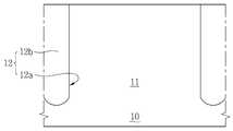
도 1a 및 1b를 참조하면, 본 발명의 실시예들에 의한 반도체 소자들(100)은 X 방향으로 연장하는 비트 라인(50L)들, 상기 X 방향에 수직하는 Y 방향으로 연장하는 게이트 라인(20L)들, 및 상기 X 방향 및 상기 Y 방향에 각각 사선의(diagonal) Z 방향으로 연장하는 바(bar) 모양의 활성 영역(11)들을 포함하고, 상기 비트 라인(50L)들과 교차하는 상기 활성 영역(11)들의 중앙 영역과 중첩하는 비트 라인 컨택 플러그(40)들 및 상기 활성 영역(11)들의 양 끝 영역들과 중첩하는 커패시터 컨택 플러그(60)들을 포함할 수 있다.1A and 1B, semiconductor devices 100 according to embodiments of the present invention include
상기 활성 영역(11)들은 도 1a에 보여지듯이 상기 Y 방향으로 서로 엇갈리도록 배치될 수도 있고, 또는 도 1b에 보여지듯이 서로 평행하도록 배치될 수도 있다.As shown in FIG. 1A, the
도 1b를 더 참조하면, 상기 활성 영역(11)들 사이에 상기 게이트 라인(20L)들과 평행하도록 상기 Y 방향으로 연장하는 소자 분리 라인(12L)들이 더 배치될 수 있다.Referring further to FIG. 1B,
도 2a 내지 2f는 본 발명의 실시예들에 의한 반도체 소자들(100A-100F)을 설명하기 위하여 도 1a의 I-I'방향 또는 도 1b의 II-II' 방향을 따라 절단한 종단면도들이다.2A to 2F are longitudinal cross-sectional views taken along a direction I-I' of FIG. 1A or a direction II-II' of FIG. 1B to describe the
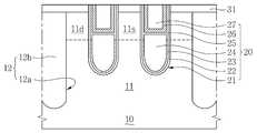
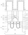
도 2a를 참조하면, 본 발명의 일 실시예에 의한 반도체 소자(100A)는 기판(10) 내에 형성된 소자 분리 영역(12)들, 게이트 구조체(20)들, 비트 라인 구조체(50), 및 커패시터 구조체(80)들을 포함할 수 있다. 상기 반도체 소자(100A)는 상기 기판(10)과 상기 비트 라인 구조체(50) 사이에 형성된 비트 라인 컨택 플러그(40)를 더 포함할 수 있다. 상기 반도체 소자(100A)는 상기 기판(10)과 상기 커패시터 구조체(80)들 사이에 형성된 커패시터 컨택 플러그(60)들을 더 포함할 수 있다. 상기 반도체 소자(100A)는 하부 층간 절연층(32), 홀 마스크 층(33), 스페이서 층(34), 상부 층간 절연층(35), 식각 정지층(36), 및 커패시터 캡핑 절연층(38)을 더 포함할 수 있다. 상기 반도체 소자(100A)는 트렌치 마스크 층(31)을 더 포함할 수 있다.Referring to FIG. 2A, a
상기 소자 분리 영역(12)들은 상기 기판(10) 내에 형성된 소자 분리 트렌치(12a)들 및 상기 소자 분리 트렌치(12a)들 내에 채워진 소자 분리 절연물(12b)을 포함할 수 있다. 상기 소자 분리 절연물(12b)은 실리콘 산화물을 포함할 수 있다. 상기 소자 분리 영역(12)들은 활성 영역(11)을 정의할 수 있다. 상기 활성 영역(11)은 상기 게이트 구조체(20)들 사이의 소스 영역(11s) 및 상기 게이트 구조체(20)들과 상기 소자 분리 영역(12)들 사이의 드레인 영역(11d)들을 포함할 수 있다. 상기 소스 영역(11s) 및 상기 드레인 영역(11d)들은 각각 인(P, phosphorous) 및/또는 비소(As, arsenic) 같은 N형 불순물을 포함할 수 있다.The
상기 게이트 구조체(20)들은 게이트 트렌치(21) 내에 형성된 게이트 절연층(22), 게이트 배리어 패턴(23), 게이트 전극 패턴(24), 전극 보호층(25), 버퍼 산화층(26), 및 게이트 캡핑 절연층(27)을 포함할 수 있다. 상기 게이트 구조체(20)들은 상기 기판(10) 내의 상기 활성 영역(11) 내에 매립(buried)될 수 있다.The
상기 게이트 트렌치(21)는 상기 기판(10)의 표면으로부터 상기 기판(10)의 내부를 향하도록 형성될 수 있다.The
상기 게이트 절연층(22)은 상기 게이트 트렌치(21)의 내벽 상에 전체적으로 컨포멀하게 형성될 수 있다. 상기 게이트 절연층(22)은 실리콘 산화물, 실리콘 질화물, 실리콘 산질화물, 또는 금속 산화물을 포함할 수 있다. 상기 금속 산화물은 하프늄 산화물, 알미늄 산화물, 또는 티타늄 산화물을 포함할 수 있다.The
상기 게이트 배리어 패턴(23)은 상기 게이트 절연층(22) 상에 컨포멀하게 형성될 수 있다. 상기 게이트 배리어 패턴(23)은 상기 게이트 트렌치(21)의 하반부에만 형성될 수 있다. 상기 게이트 배리어 패턴(23)은 티타늄 질화물(TiN) 또는 탄탈륨 질화물(TaN) 같은 배리어용 금속 화합물을 포함할 수 있다.The
상기 게이트 전극 패턴(24)은 상기 게이트 트렌치(21)를 부분적으로 채우도록 상기 게이트 배리어 패턴(23) 상에 형성될 수 있다. 예를 들어, 상기 게이트 전극 패턴(24)은 상기 게이트 트렌치(21)의 하반부를 채울 수 있다. 상기 게이트 전극 패턴(24)은 텅스텐 또는 구리 같은 금속을 포함할 수 있다.The
상기 게이트 배리어 패턴(23)의 상단부는 상기 게이트 전극 패턴(24)의 상단부보다 낮게 리세스될 수 있다. 상기 게이트 배리어 패턴(23)의 상단부가 리세스됨으로써, 상기 게이트 전극 패턴(24)과 상기 소스 영역(11s)의 거리 및 상기 게이트 전극 패턴(24)과 상기 드레인 영역(11d)들 간의 거리가 증가할 수 있다. 따라서, 상기 게이트 구조체(20)가 턴온(turn on)됨에 따라 발생하는 GIDL(gate induced drain leakage current)가 감소할 수 있다.The upper end of the
상기 전극 보호층(25)은 상기 게이트 트렌치(21)의 상반부의 상기 게이트 절연층(22) 상에 컨포멀하게 형성될 수 있다. 상기 전극 보호층(25)은 상기 리세스된 게이트 배리어 패턴(23)의 상단부 상에 형성될 수 있다. 예를 들어, 상기 전극 보호층(25)의 일부는 상기 게이트 전극 패턴(24)과 상기 게이트 절연층(22) 사이에 개재될 수 있다. 상기 전극 보호층(25)은 실리콘 질화물을 포함할 수 있다. 상기 전극 보호층(25)은 상기 게이트 전극 패턴(24)과 상기 버퍼 산화층(26) 사이에 개재되어 상기 버퍼 산화층(26)으로부터 상기 게이트 전극 패턴(24)으로 산소 원자들 또는 산소 이온들이 확산하는 것을 방지(prevent), 저지(retard), 또는 완화(mitigate)할 수 있다.The
상기 버퍼 산화층(26)은 상기 전극 보호층(25) 상에 컨포멀하게 형성될 수 있다. 상기 버퍼 산화층(26)은 실리콘 산화물을 포함할 수 있다. 예를 들어, 상기 버퍼 산화층(26)은 PSG(phosphorous silicate glass) 같은 도핑된 실리콘 산화물 또는 인(P, phosphorous) 같은 도펀트들을 포함할 수 있다. 상기 버퍼 산화층(26)은 이온 주입 소스가 될 수 있다. 구체적으로, 상기 버퍼 산화층(26)에 함유된 상기 도펀트들은 제조 공정 중에 상기 활성 영역(11)으로 확산하여 상기 소스 영역(11s) 및 상기 드레인 영역(11d)들을 형성할 수 있다. 따라서 물리적으로 이온들을 주입하는 이온 임플란테이션 공정이 배제되므로, 상기 활성 영역(11)의 표면이 물리적으로 손상되는 것이 방지되고 및 거리에 따라 점진적으로 변화하는 도핑 프로파일이 얻어질 수 있다.The
상기 게이트 캡핑 절연층(27)은 상기 게이트 트렌치(21)를 채우도록 상기 버퍼 산화층(26) 상에 형성될 수 있다. 상기 게이트 캡핑 절연층(27)은 실리콘 질화물을 포함할 수 있다.The gate capping insulating
상기 게이트 캡핑 절연층(27)은 상기 기판(10)의 상기 활성 영역(11)에 컴프레시브 스트레스(compressive stress)를 줄 수 있다. 상기 버퍼 산화층(26)은 상기 컴프레시브 스트레스를 완화시킬 수 있다. 따라서, 상기 컴프레시브 스트레스에 의한 상기 활성 영역(11)의 N형 캐리어의 이동도 (mobility)가 저하되는 것이 완화될 수 있다.The gate capping insulating
상기 버퍼 산화층(26)은 상기 게이트 캡핑 절연층(27)보다 소프트하고 유연하므로 기판(10)과 게이트 캡핑 절연층(27)의 열 팽창 계수의 차이에 따른 부(-)적인 현상들이 방지 또는 완화될 수 있다.Since the
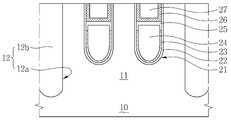
상기 비트 라인 컨택 플러그(40)는 상기 기판(10)의 상기 활성 영역(11)의 상기 소스 영역(11s) 상에 형성될 수 있다. 상기 비트 라인 컨택 플러그(40)의 하면은 상기 기판(10)의 내부에 위치할 수 있다. 예를 들어, 상기 비트 라인 컨택 플러그(40)의 하부는 상기 기판(10)의 상면보다 낮게 아래로 돌출할 수 있다. 상기 비트 라인 컨택 플러그(40)의 상기 하면의 외측부들은 상기 게이트 구조체(20)들과 접촉할 수 있다. 예를 들어, 상기 비트 라인 컨택 플러그(40)의 하면의 측부 및/또는 측면의 하부는 상기 게이트 구조체(20)들의 상기 게이트 절연층(22), 상기 전극 보호층(25), 상기 버퍼 산화층(26), 및 상기 게이트 캡핑 절연층(27)과 접촉할 수 있다. 다른 말로, 상기 비트 라인 컨택 플러그(40)의 상기 하면이 상기 기판(10) 내에 위치할 수 있도록, 상기 기판(10)의 상기 활성 영역(11)의 상기 소스 영역(11s)의 상면이 리세스될 수 있다. 또한, 상기 게이트 구조체(20)들의 상기 게이트 절연층(22), 상기 전극 보호층(25), 상기 버퍼 산화층(26), 및 상기 게이트 캡핑 절연층(27)의 상면들이 경사지도록(slanted) 부분적으로 리세스될 수 있다. 예를 들어, 상기 비트 라인 구조체(50)와 수직으로 정렬 또는 중첩하지 않고 노출되는 부분들이 순방향으로 경사질(slanted) 수 있다. 상기 비트 라인 컨택 플러그(40)의 외곽부들이 리세스됨으로써, 다른 전도성 구성 요소들과 단락(short)되는 것이 방지될 수 있다. 상기 비트 라인 컨택 플러그(40)는 상기 게이트 구조체(20)들의 간격, 예를 들어, 상기 소스 영역(11s)의 수평 폭보다 넓은 수평 폭을 가질 수 있다. 상기 비트 라인 컨택 플러그(40)는 상기 기판(10)의 상기 활성 영역(11)의 상기 소스 영역(11s)과 상기 비트 라인 구조체(50)를 전기적으로 연결할 수 있다.The bit
보호 절연층(45)이 상기 비트 라인 컨택 플러그(40)의 상기 경사진(slanted) 면들 상에 형성될 수 있다. 상기 보호 절연층(45)은 실리콘 산화물, 예를 들어, 자연 산화물을 포함할 수 있다. 상기 보호 절연층(45)은 상기 비트 라인 컨택 플러그(40)와 다른 전도성 구성 요소들이 전기적으로 단락되는 현상을 방지하고, 제조 공정 중 상기 비트 라인 컨택 플러그(40)가 받는 물리적 및 화학적 공격으로부터 보호할 수 있다.A protective insulating
상기 트렌치 마스크 층(31)은 상기 비트 라인 컨택 플러그(40) 및 상기 커패시터 컨택 플러그(60)들의 측면들을 감싸도록 상기 기판(10) 및/또는 상기 소자 분리 영역(12)들 상에 형성될 수 있다. 상기 게이트 구조체(20)들의 상면 및 상기 트렌치 마스크 층(31)의 상면은 공면을 가질 수 있다.(be co-planar) 상기 트렌치 마스크 층(31)은 실리콘 산화물 또는 실리콘 질화물을 포함할 수 있다.The
상기 하부 층간 절연층(32)은 상기 비트 라인 컨택 플러그(40) 및 상기 커패시터 컨택 플러그(60)들의 측면들을 감싸도록 상기 트렌치 마스크 층(31) 상에 형성될 수 있다. 상기 하부 층간 절연층(32)은 실리콘 산화물 또는 실리콘 질화물을 포함할 수 있다. 예를 들어, 상기 트렌치 마스크 층(31)과 상기 하부 층간 절연층(32)이 동일한 물질로 형성될 경우, 상기 트렌치 마스크 층(31)과 상기 하부 층간 절연층(32) 사이의 계면(boundary)이 사라질 수 있다.The lower
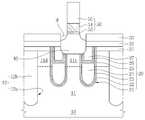
상기 비트 라인 구조체(50)들은 비트 라인 배리어 패턴(53), 비트 라인 전극 패턴(54), 및 비트 라인 캡핑 패턴(55)을 포함할 수 있다. 상기 비트 라인 배리어 패턴(53)은 상기 비트 라인 컨택 플러그(40)와 접촉하여 전기적으로 연결될 수 있다. 상기 비트 라인 배리어 패턴(53)은 티타늄(Ti), 티타늄 질화물(TiN), 티타늄 실리사이드(TiSi), 탄탈륨(Ta), 탄탈륨 질화물(TaN), 탄탈륨 실리사이드(TaSi), 니켈 실리사이드(NiSi), 코발트 실리사이드(CoSi), 텅스텐 질화물(WN), 또는 텅스텐 실리사이드(WSi) 같은 금속 또는 금속 화합물을 포함할 수 있다. 상기 비트 라인 전극 패턴(54)은 텅스텐 또는 구리 같은 금속을 포함할 수 있다. 상기 비트 라인 캡핑층(55a)은 실리콘 질화물을 포함할 수 있다. 상기 비트 라인 배리어 패턴(53), 상기 비트 라인 전극 패턴(54), 및 상기 비트 라인 캡핑 패턴(55)의 측벽들은 수직으로 정렬될 수 있다.The
상기 스페이서 층(34)은 상기 비트 라인 구조체(50)를 감쌀 수 있다. 예를 들어, 상기 스페이서 층(34)은 상기 비트 라인 구조체(50)의 상면 및 측면들 상에 컨포멀하게 형성될 수 있다. 상기 스페이서 층(34)은 상기 비트 라인 컨택 플러그(40)의 상기 리세스된 경사진(slanted) 면들을 덮을 수 있다. 상기 스페이서 층(34)은 상기 하부 층간 절연층(32) 상으로 수평으로 연장하도록 형성될 수 있다. 상기 스페이서 층(34)은 실리콘 질화물을 포함할 수 있다.The
상기 상부 층간 절연층(35)은 상기 스페이서 층(34)의 측면들을 감쌀 수 있다. 상기 스페이서 층(34)의 상면 및 상기 상부 층간 절연층(35)의 상면은 공면을 가질 수 있다. (be co-planar)The upper
상기 커패시터 컨택 플러그(60)들은 상기 상부 층간 절연층(35), 상기 스페이서 층(34), 상기 하부 층간 절연층(32), 및 상기 트렌치 마스크 층(31)을 수직으로 관통하여 상기 기판(10)의 상기 활성 영역(11)의 상기 드레인 영역(11d)들과 각각 연결되도록 정렬될 수 있다. 상기 커패시터 컨택 플러그(60)들의 하면들은 상기 기판(10)의 내부에 위치할 수 있다. 상기 커패시터 컨택 플러그(60)들의 상기 하면의 외측부들은 상기 게이트 구조체(20)들 및 상기 소자 분리 영역(12)들과 접촉할 수 있다. 예를 들어, 상기 커패시터 컨택 플러그(60)들은 상기 게이트 구조체(20)들의 상기 게이트 절연층(22), 상기 전극 보호층(25), 상기 버퍼 산화층(26), 및 상기 게이트 캡핑 절연층(27)과 접촉할 수 있다. 다른 말로, 상기 커패시터 컨택 플러그(60)들의 상기 하면들이 상기 기판(10) 내에 위치할 수 있도록, 상기 기판(10)의 상기 활성 영역(11)의 상기 드레인 영역(11d)들의 상면들이 리세스될 수 있다. 또한, 상기 게이트 구조체(20)들의 상기 게이트 절연층(22), 상기 전극 보호층(25), 상기 버퍼 산화층(26), 및 상기 게이트 캡핑 절연층(27)의 상면들이 부분적으로 리세스될 수 있다. 상기 커패시터 컨택 플러그(60)들은 상기 게이트 구조체(20)들과 상기 소자 분리 영역(12)들의 간격들, 예를 들어, 상기 드레인 영역(11d)들의 수평 폭들보다 넓은 수평 폭들을 가질 수 있다. 상기 커패시터 컨택 플러그(60)들은 상기 기판(10)의 상기 활성 영역(11)의 상기 드레인 영역(11d)들과 상기 커패시터 구조체(80)들을 각각 전기적으로 연결할 수 있다. 상기 스페이서 층(34), 상기 상부 층간 절연층(35)의 상면, 및/또는 상기 커패시터 컨택 플러그(60)의 상면은 공면을 가질 수 있다. (be co-planar)The capacitor contact plugs 60 vertically penetrate the upper
상기 식각 정지층(36)은 상기 비트 라인 구조체(50) 및 상기 상부 층간 절연층(35) 상에 형성될 수 있다. 상기 식각 정지층(36)은 상기 비트 라인 구조체(50)의 상부, 예를 들어, 상기 비트 라인 캡핑 패턴(55) 또는 상기 스페이서 층(34) 상에 형성될 수 있다. 상기 식각 정지층(36)은 실리콘 질화물을 포함할 수 있다.The
상기 커패시터 구조체(80)들은 각각 커패시터 하부 전극(81), 커패시터 유전층(83), 및 커패시터 상부 전극(85)을 포함할 수 있다. 상기 커패시터 하부 전극(81)들은 상기 커패시터 컨택 플러그(60)들과 각각 전기적으로 연결 및 수직으로 정렬될 수 있다. 상기 커패시터 하부 전극(81)은 상기 식각 정지층(36)을 수직으로 관통할 수 있다. 상기 커패시터 하부 전극(81)은 도핑된 다결정 실리콘, 금속, 또는 금속 화합물 같은 전도체를 포함할 수 있다. 상기 커패시터 유전층(83)은 상기 커패시터 하부 전극(81)의 표면을 컨포멀하게 덮을 수 있다. 예를 들어, 상기 커패시터 유전층(83)은 상기 커패시터 하부 전극(81)의 상면 및 측면들 상에 형성될 수 있다. 상기 커패시터 유전층(83)은 상기 식각 정지층(36) 상으로 연장할 수 있다. 다른 말로, 상기 커패시터 유전층(83)은 상기 식각 정지층(36)의 표면 상에 컨포멀하게 형성될 수 있다. 상기 커패시터 유전층(83)은 하프늄 산화물, 알루미늄 산화물, 티타늄 산화물, 탄탈륨 산화물, 루데늄 산화물, 또는 란탄 산화물 같은 금속 산화물, 또는 실리콘 산화물 및 실리콘 질화물 중 어느 하나를 포함할 수 있다. 상기 커패시터 상부 전극(85)은 상기 커패시터 유전층(83) 상에 컨포멀하게 형성될 수 있다. 상기 커패시터 상부 전극(85)은 금속 또는 금속 화합물을 포함할 수 있다.Each of the capacitor structures 80 may include a capacitor
상기 커패시터 캡핑 절연층(38)은 상기 커패시터 구조체(80)들의 사이를 채우고 상기 커패시터 구조체(80)들을 덮을 수 있다. 상기 커패시터 캡핑 절연층(38)은 실리콘 산화물을 포함할 수 있다.The capacitor capping insulating
위에서 언급되었듯이, 상기 게이트 배리어 패턴(23)의 상단부가 상기 게이트 전극 패턴(24)의 상단부보다 낮게 리세스됨으로써, 상기 게이트 전극 패턴(24)과 상기 소스 영역(11s)의 거리 및 상기 게이트 전극 패턴(24)과 상기 드레인 영역(11d)들 간의 거리가 증가할 수 있다. 따라서, 상기 게이트 구조체(20)가 턴온(turn on)됨에 따라 발생하는 GIDL(gate induced drain leakage current)가 감소할 수 있다.As mentioned above, the upper end of the
상기 전극 보호층(25)이 상기 게이트 전극 패턴(24)과 상기 버퍼 산화층(26) 사이에 개재됨으로써, 상기 버퍼 산화층(26)으로부터 상기 게이트 전극 패턴(24)으로 산소 원자들 또는 산소 이온들이 확산하여 상기 게이트 전극 패턴(24)을 산화시키는 것이 방지(prevent), 저지(retard), 또는 완화(mitigate)될 수 있다.As the
상기 버퍼 산화층(26)이 인(P, phosphorous) 같은 N형 도펀트들을 포함함으로써, 상기 소스 영역(11s) 및 상기 드레인 영역(11d)들이 확산 공정을 이용하여 형성될 수 있다. 상기 버퍼 산화층(26)이 상기 전극 보호층(25) 및 상기 게이트 캡핑 절연층(27)보다 소프트하고 유연한 물질로 형성됨으로써, 상기 게이트 캡핑 절연층(27)으로부터 상기 활성 영역(11)에 가해지는 컴프레시브 스트레스가 완화될 수 있고 및 상기 활성 영역(11)의 N형 캐리어의 이동도가 저하되는 것이 방지 및 완화될 수 있다.Since the
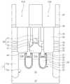
도 2b를 참조하면, 본 발명의 일 실시예에 의한 반도체 소자(100B)는 기판(10) 내에 형성된 소자 분리 영역(12)들, 게이트 구조체(20)들, 비트 라인 구조체(50), 및 커패시터 구조체(80)들을 포함할 수 있다. 상기 반도체 소자(100B)는 상기 기판(10)과 상기 비트 라인 구조체(50) 사이에 형성된 비트 라인 컨택 플러그(40)를 더 포함할 수 있다. 상기 반도체 소자(100B)는 상기 기판(10)과 상기 커패시터 구조체(80)들 사이에 형성된 커패시터 컨택 플러그(60)들을 더 포함할 수 있다. 상기 반도체 소자(100B)는 하부 층간 절연층(32), 홀 마스크 층(33), 스페이서 층(34), 상부 층간 절연층(35), 식각 정지층(36), 및 커패시터 캡핑 절연층(38)을 더 포함할 수 있다. 상기 하부 층간 절연층(32)은 상기 기판(10) 및/또는 상기 소자 분리 영역(12)들 상에 직접적으로 형성될 수 있다. 설명되지 않은 구성 요소들은 도 2a를 참조하면 이해될 수 있을 것이다.Referring to FIG. 2B, the
도 2c를 참조하면, 본 발명의 일 실시예에 의한 반도체 소자(100C)는 기판(10) 내에 형성된 소자 분리 영역(12)들, 게이트 구조체(20)들, 비트 라인 구조체(50), 및 커패시터 구조체(80)들을 포함할 수 있다. 상기 반도체 소자(100C)는 상기 기판(10)과 상기 비트 라인 구조체(50) 사이에 형성된 비트 라인 컨택 플러그(40)를 더 포함할 수 있다. 상기 반도체 소자(100C)는 상기 기판(10)과 상기 커패시터 구조체(80)들 사이에 형성된 커패시터 컨택 플러그(60)들을 더 포함할 수 있다. 상기 반도체 소자(100C)는 하부 층간 절연층(32), 홀 마스크 층(33), 스페이서 층(34), 상부 층간 절연층(35), 식각 정지층(36), 및 커패시터 캡핑 절연층(38)을 더 포함할 수 있다. 상기 반도체 소자(100C)는 트렌치 마스크 층(31)을 더 포함할 수 있다.2C, a semiconductor device 100C according to an embodiment of the present invention includes
상기 게이트 구조체(20)들은 게이트 트렌치(21) 내에 형성된 게이트 절연층(22), 게이트 배리어 패턴(23), 게이트 전극 패턴(24), 버퍼 산화층(26), 및 게이트 캡핑 절연층(27)을 포함할 수 있다. 상기 버퍼 산화층(26)은 상기 게이트 절연층(22) 상에 직접적으로 컨포멀하게 형성될 수 있다.The
상기 게이트 배리어 패턴(23)의 상단부는 상기 게이트 전극 패턴(24)의 상단부보다 낮게 리세스될 수 있다. 상기 버퍼 산화층(26)은 상기 리세스된 게이트 배리어 패턴(23)의 상단부 상에 형성될 수 있다. 예를 들어, 상기 버퍼 산화층(26)의 일부는 상기 게이트 전극 패턴(24)과 상기 게이트 절연층(22) 사이에 개재될 수 있다. 상기 버퍼 산화층(26)은 상기 게이트 배리어 패턴(23) 및 상기 게이트 전극 패턴(24)과 접촉할 수 있다. 상기 게이트 전극 패턴(24)이 내산화성 금속을 포함하는 경우, 도 2a 및 2b의 상기 전극 보호층(25)이 생략될 수 있다. 설명되지 않은 구성 요소들은 도 2a를 참조하면 이해될 수 있을 것이다.The upper end of the
도 2d를 참조하면, 본 발명의 일 실시예에 의한 반도체 소자(100D)는 기판(10) 내에 형성된 소자 분리 영역(12)들, 게이트 구조체(20)들, 비트 라인 구조체(50), 및 커패시터 구조체(80)들을 포함할 수 있다. 상기 반도체 소자(100D)는 상기 기판(10)과 상기 비트 라인 구조체(50) 사이에 형성된 비트 라인 컨택 플러그(40)를 더 포함할 수 있다. 상기 반도체 소자(100D)는 상기 기판(10)과 상기 커패시터 구조체(80)들 사이에 형성된 커패시터 컨택 플러그(60)들을 더 포함할 수 있다. 상기 반도체 소자(100D)는 하부 층간 절연층(32), 홀 마스크 층(33), 스페이서 층(34), 상부 층간 절연층(35), 식각 정지층(36), 및 커패시터 캡핑 절연층(38)을 더 포함할 수 있다.Referring to FIG. 2D, a
상기 게이트 구조체(20)들은 게이트 트렌치(21) 내에 형성된 게이트 절연층(22), 게이트 배리어 패턴(23), 게이트 전극 패턴(24), 버퍼 산화층(26), 및 게이트 캡핑 절연층(27)을 포함할 수 있다. 상기 버퍼 산화층(26)은 상기 게이트 절연층(22) 상에 직접적으로 컨포멀하게 형성될 수 있다. 상기 버퍼 산화층(26)은 상기 게이트 배리어 패턴(23) 및 상기 게이트 전극 패턴(24)과 접촉할 수 있다. 상기 게이트 전극 패턴(24)이 내산화성 금속을 포함하는 경우, 도 2a 및 2b의 상기 전극 보호층(25)이 생략될 수 있다.The
상기 하부 층간 절연층(32)은 상기 기판(10) 및/또는 상기 소자 분리 영역(12)들 상에 직접적으로 형성될 수 있다. 설명되지 않은 구성 요소들은 도 2a를 참조하면 이해될 수 있을 것이다.The lower
도 2e를 참조하면, 본 발명의 일 실시예에 의한 반도체 소자(100E)는 기판(10) 내에 형성된 소자 분리 영역(12)들, 게이트 구조체(20)들, 비트 라인 구조체(50), 및 커패시터 구조체(80)들을 포함할 수 있다. 상기 반도체 소자(100E)는 상기 기판(10)과 상기 비트 라인 구조체(50) 사이에 형성된 비트 라인 컨택 플러그(40)를 더 포함할 수 있다. 상기 반도체 소자(100E)는 상기 기판(10)과 상기 커패시터 구조체(80)들 사이에 형성된 커패시터 컨택 플러그(60)들을 더 포함할 수 있다. 상기 반도체 소자(100E)는 하부 층간 절연층(32), 홀 마스크 층(33), 스페이서 층(34), 상부 층간 절연층(35), 식각 정지층(36), 및 커패시터 캡핑 절연층(38)을 더 포함할 수 있다. 상기 반도체 소자(100E)는 트렌치 마스크 층(31)을 더 포함할 수 있다.Referring to FIG. 2E, a
상기 게이트 구조체(20)들은 게이트 트렌치(21) 내에 형성된 게이트 절연층(22), 게이트 배리어 패턴(23), 게이트 전극 패턴(24), 전극 보호층(25), 버퍼 산화층(26), 및 게이트 캡핑 절연층(27)을 포함할 수 있다. 상기 게이트 배리어 패턴(23)의 상단부는 상기 게이트 전극 패턴(24)의 상단부보다 낮게 리세스될 수 있다.The
상기 전극 보호층(25)은 상기 게이트 전극 패턴(24)과 상기 버퍼 산화층(25) 사이에 개재될 수 있다. 상기 전극 보호층(25)은 실질적으로 평탄한 표면을 가질 수 있다. 상기 전극 보호층(25)은 상기 게이트 전극 패턴(24)의 상면을 덮고, 및 상기 게이트 절연층(22)과 상기 게이트 전극 패턴(24)의 사이의 상기 리세스된 게이트 배리어 패턴(23) 상에 개재될 수 있다. 예를 들어, 상기 전극 보호층(25)은 상기 게이트 트렌치(21)의 측벽들 상의 상기 게이트 절연층(22) 상에 실질적으로 형성되지 않을 수 있다.The
상기 버퍼 산화층(26)은 상기 게이트 트렌치(21)의 측벽들 상의 상기 게이트 절연층(22) 상에 직접적으로 컨포멀하게 형성될 수 있다. 상기 버퍼 산화층(26)은 상기 게이트 배리어 패턴(23) 및 상기 게이트 전극 패턴(24)과 접촉하지 않을 수 있다.The
상기 게이트 캡핑 절연층(27)은 상기 게이트 트렌치(21)의 상부 영역에서 상기 게이트 절연층(22)와 접촉할 수 있다. 설명되지 않은 구성 요소들은 도 2a를 참조하면 이해될 수 있을 것이다.The gate capping insulating
도 2f를 참조하면, 본 발명의 일 실시예에 의한 반도체 소자(100F)는 기판(10) 내에 형성된 소자 분리 영역(12)들, 게이트 구조체(20)들, 비트 라인 구조체(50), 및 커패시터 구조체(80)들을 포함할 수 있다. 상기 반도체 소자(100F)는 상기 기판(10)과 상기 비트 라인 구조체(50) 사이에 형성된 비트 라인 컨택 플러그(40)를 더 포함할 수 있다. 상기 반도체 소자(100F)는 상기 기판(10)과 상기 커패시터 구조체(80)들 사이에 형성된 커패시터 컨택 플러그(60)들을 더 포함할 수 있다. 상기 반도체 소자(100F)는 하부 층간 절연층(32), 홀 마스크 층(33), 스페이서 층(34), 상부 층간 절연층(35), 식각 정지층(36), 및 커패시터 캡핑 절연층(38)을 더 포함할 수 있다.Referring to FIG. 2F, a semiconductor device 100F according to an embodiment of the present invention includes
상기 게이트 구조체(20)들은 게이트 트렌치(21) 내에 형성된 게이트 절연층(22), 게이트 배리어 패턴(23), 게이트 전극 패턴(24), 버퍼 산화층(26), 및 게이트 캡핑 절연층(27)을 포함할 수 있다.The
상기 게이트 배리어 패턴(23)의 상단부는 상기 게이트 전극 패턴(24)의 상단부보다 낮게 리세스될 수 있다.The upper end of the
상기 전극 보호층(25)은 상기 게이트 전극 패턴(24)과 상기 버퍼 산화층(25) 사이에 개재될 수 있다. 상기 전극 보호층(25)은 실질적으로 평탄한 표면을 가질 수 있다. 상기 전극 보호층(25)은 상기 게이트 전극 패턴(24)의 상면을 덮고, 및 상기 게이트 절연층(22)과 상기 게이트 전극 패턴(24)의 사이의 상기 리세스된 게이트 배리어 패턴(23) 상에 개재될 수 있다. 예를 들어, 상기 전극 보호층(25)은 상기 게이트 트렌치(21)의 측벽들 상의 상기 게이트 절연층(22) 상에 실질적으로 형성되지 않을 수 있다.The
상기 버퍼 산화층(26)은 상기 게이트 트렌치(21)의 측벽들 상의 상기 게이트 절연층(22) 상에 직접적으로 컨포멀하게 형성될 수 있다. 상기 버퍼 산화층(26)은 상기 게이트 배리어 패턴(23) 및 상기 게이트 전극 패턴(24)과 접촉하지 않을 수 있다.The
상기 게이트 캡핑 절연층(27)은 상기 게이트 트렌치(21)의 상부 영역에서 상기 게이트 절연층(22)와 접촉할 수 있다.The gate capping insulating
상기 하부 층간 절연층(32)은 상기 기판(10) 및/또는 상기 소자 분리 영역(12)들 상에 직접적으로 형성될 수 있다. 설명되지 않은 구성 요소들은 도 2a를 참조하면 이해될 수 있을 것이다.The lower
도 2e 및 도 2f에 도시된 상기 반도체 소자들(100E, 100F)에서, 상기 게이트 산화 방지층(25)이 상기 게이트 트렌치(21)의 측벽들과 접촉하는 면적이 최소화되므로, 상기 게이트 산화 방지층(25)이 상기 활성 영역(11)의 상기 소스 영역(11s) 및 상기 드레인 영역들(11d)에 가하는 컴프레시브 스트레스가 최소화될 수 있다.In the
도 3a 내지 3o는 본 발명의 일 실시예에 의한 반도체 소자를 제조하는 방법을 설명하기 위하여 도 1a의 I-I' 또는 도 1b의 II-II' 방향을 따라 절단한 종단면도들이다.3A to 3O are longitudinal cross-sectional views taken along a direction I-I' of FIG. 1A or II-II' of FIG. 1B in order to explain a method of manufacturing a semiconductor device according to an embodiment of the present invention.
도 3a를 참조하면, 본 발명의 일 실시예에 의한 반도체 소자(100A)를 제조하는 방법은 예를 들어, STI (shallow trench isolation) 공정을 수행하여 기판(10) 내에 활성 영역(11)을 정의하는 소자 분리 영역(12)들을 형성하는 것을 포함할 수 있다. 상기 STI 공정은 상기 기판(10) 내에 소자 분리 트렌치(12a)를 형성하고, 상기 소자 분리 트렌치(12a) 내에 실리콘 산화물 같은 소자 분리 절연물(12b)을 채우는 것을 포함할 수 있다.Referring to FIG. 3A, a method of manufacturing a
도 3b를 참조하면, 상기 방법은 상기 기판(10) 상에 트렌치 마스크 층(31)을 형성하고, 및 상기 트렌치 마스크 층(31)을 식각 마스크로 이용하는 식각 공정을 수행하여 상기 기판(10) 내에 게이트 트렌치(21)들을 형성하는 것을 포함할 수 있다. 상기 트렌치 마스크 층(31)은 HDP(High Density Plasma) 공정을 이용하여 형성된 실리콘 산화물 같이 비교적 치밀한 실리콘 산화물을 포함할 수 있다.Referring to FIG. 3B, the method includes forming a
도 3c를 참조하면, 상기 방법은 상기 게이트 트렌치(21)들 내벽들 및 상기 트렌치 마스크 층(31)의 표면 상에 게이트 절연층(22)을 컨포멀하게 형성하는 것을 포함할 수 있다. 상기 게이트 절연층(22)은 실리콘 산화물 또는 금속 산화물을 포함할 수 있다. 상기 금속 산화물은 하프늄 산화물, 알미늄 산화물, 또는 티타늄 산화물을 포함할 수 있다. 상기 게이트 절연층(22)은 ALD(atomic layered deposition; 원자층 증착) 공정 및/또는 열 산화 공정을 이용하여 형성될 수 있다. 상기 열 산화 공정을 수행하여 상기 게이트 절연층(22)이 형성될 경우, 상기 트렌치 마스크 층(31)의 표면 상에는 상기 게이트 절연층(22)이 형성되지 않을 수도 있다.Referring to FIG. 3C, the method may include conformally forming a
도 3d를 참조하면, 상기 방법은 상기 게이트 절연층(22) 상에 게이트 배리어 층(23a)을 컨포멀하게 형성하고, 및 상기 게이트 배리어 층(23a) 상에 상기 게이트 트렌치(21)를 채우는 게이트 전극층(24a)을 형성하는 것을 포함할 수 있다. 상기 게이트 배리어 층(23a)은 ALD 공정을 수행하여 형성될 수 있다. 상기 게이트 전극층(24a)은 ALD 또는 CVD(chemical vapor deposition) 공정을 수행하여 형성될 수 있다. 상기 게이트 배리어 층(23a)은 티타늄 질화물(TiN) 또는 탄탈륨 질화물(TaN) 같은 배리어용 금속 화합물을 포함할 수 있다. 상기 게이트 전극층(24a)은 텅스텐 또는 구리 같은 금속을 포함할 수 있다.Referring to FIG. 3D, the method comprises forming a gate barrier layer 23a conformally on the
도 3e를 참조하면, 상기 방법은 에치-백 공정을 수행하여 상기 게이트 트렌치(21) 내의 상기 게이트 배리어 층(23a) 및 상기 게이트 전극층(24a)의 상부들을 부분적으로 제거하여 게이트 전극 패턴(24) 및 게이트 배리어 패턴(23)을 형성하는 것을 포함할 수 있다. 상기 게이트 전극 패턴(24)의 상면은 상기 게이트 배리어 패턴(23)의 상단보다 높은 레벨에 위치할 수 있다. 다른 말로, 상기 게이트 배리어 패턴(23)의 상기 상단은 상기 게이트 전극 패턴(24)의 상기 상면보다 낮게 리세스될 수 있다. 따라서, 상기 게이트 절연층(22)과 상기 게이트 전극 패턴(24) 사이에 갭(g)이 형성될 수 있다.Referring to FIG. 3E, in the method, the
상기 에치-백 공정은 습식 식각 공정을 포함할 수 있다. 상기 습식 식각 공정은 상기 게이트 전극층(24a)을 주로 제거하는 제1 식각제(etchant), 및 상기 게이트 배리어 층(23a)을 주로 식각하는 제2 식각제을 포함하는 식각액(etching solution)을 이용하여 한 번 또는 두 번으로 수행될 수 있다. 예를 들어, 상기 습식 식각 공정은, 상기 제1 식각제를 포함하는 식각액을 이용하는 1차 식각 공정을 수행한 후, 연속적으로 상기 제2 식각제를 포함하는 식각액을 이용하는 제2 식각 공정을 수행하는 것을 포함할 수 있다. 상기 제1 식각제는 물, 과산화수소 (H2O2) 및/또는 암모늄(NH4)을 포함할 수 있다. 상기 제2 식각제는 물 및 황산(H2SO4)을 포함할 수 있다. 상기 제2 식각제는 과산화수소 (H2O2) 및/또는 암모늄(NH4)도 포함할 수 있다.The etch-back process may include a wet etching process. The wet etching process is performed by using an etching solution including a first etchant that mainly removes the
도 3f를 참조하면, 상기 방법은 상기 게이트 트렌치(21) 내부의 상기 게이트 절연층(22) 및 상기 게이트 전극 패턴(24) 상에 전극 보호층(25)을 형성하고, 상기 전극 보호층(25) 상에 버퍼 산화층(26)을 형성하고, 및 상기 버퍼 산화층(26) 상에 게이트 캡핑 절연층(27)을 형성하는 것을 포함할 수 있다.Referring to FIG. 3F, the method comprises forming an electrode
상기 전극 보호층(25)은 상기 갭(g)을 채울 수 있다. 상기 전극 보호층(25)은 상기 트렌치 마스크 층(31) 상에도 형성될 수 있다. 상기 전극 보호층(25)은 ALD 공정을 이용하여 컨포멀하게 형성될 수 있다. 상기 전극 보호층(25)은 실리콘 질화물을 포함할 수 있다.The
상기 버퍼 산화층(26)은 ALD 공정을 이용하여 컨포멀하게 형성될 수 있다. 상기 버퍼 산화층(26)은 도펀트를 포함할 수 있다. 상기 도펀트는 PSG (phosphorous silicate glass), N-doped oxide 같이 P(phosphorous) 또는 As(arsenic) 같은 N형 불순물을 충분히 포함할 수 있다. 예를 들어, 상기 버퍼 산화층(26)은 P(phosphorous)를 총 중량 또는 부피의 약 20% 정도까지 포함할 수 있다. 상기 버퍼 산화층(26)은 B(boron) 같은 P형 불순물을 실질적으로 포함하지 않는다.The
상기 게이트 캡핑 절연층(27)은 상기 게이트 트렌치(21)를 완전히 채울 수 있다. 상기 게이트 캡핑 절연층(27)은 실리콘 질화물을 포함할 수 있다.The gate capping insulating
이후, 열적 어닐링 공정을 더 수행하여 소스 영역(11s) 및 드레인 영역(11d)들을 형성하는 것을 포함할 수 있다. 상기 소스 영역(11s) 및 상기 드레인 영역(11d)들은 상기 버퍼 산화층(26) 내의 도펀트가 상기 기판(10)으로 확산하여 형성될 수 있다. 상기 확산 공정을 이용하여 형성된 상기 소스 영역(11s) 및 상기 드레인 영역(11d)들은 거리에 따라 점진적으로 변화하는 도펀트 농도를 가질 수 있으므로, 안정적인 전기적 특성을 가질 수 있다. 상기 활성 영역(11)에 물리적 손상을 주는 이온 임플란테이션 공정을 수행하지 않으므로, 상기 소스 영역(11s) 및 상기 드레인 영역(11d)들은 양호한 물리적 및 전기적 특성을 가질 수 있다.Thereafter, a thermal annealing process may be further performed to form the
상기 게이트 캡핑 절연층(27) 및/또는 상기 전극 보호층(25)이 실리콘 질화물을 포함하는 경우, 상기 게이트 캡핑 절연층(27)은 상기 기판(10)에 컴프레시브 스트레스를 줄 수 있다. 상기 버퍼 산화층(26)은 상기 게이트 캡핑 절연층(27) 및 상기 전극 보호층(25)보다 유연하기 때문에 상기 컴프레시브 스트레스를 완화할 수 있다. 상기 기판(10)이 컴프레시브 스트레스를 받을 경우, 상기 기판(10) 내의 전자들의 이동도가 저하된다. 상기 버퍼 산화층(26)이 상기 컴프레시브 스트레스를 완화시켜주기 때문에 상기 전자들의 이동도의 저하가 완화될 수 있다.When the gate capping insulating
도 3g를 참조하면, 상기 방법은 평탄화 공정을 수행하여 상기 트렌치 마스크 층(31) 상의 상기 게이트 캡핑 절연층(27), 상기 버퍼 산화층(26), 및 상기 전극 보호층(25)을 제거하여 상기 게이트 트렌치(21) 내에 형성된 상기 게이트 절연층(22), 상기 게이트 배리어 패턴(23), 상기 게이트 전극 패턴(24), 상기 전극 보호층(25), 상기 버퍼 산화층(26), 및 상기 게이트 캡핑 절연층(27)을 포함하는 게이트 구조체(20)를 형성하는 것을 포함할 수 있다. 상기 평탄화 공정은 CMP(chemical mechanical polishing) 공정을 포함할 수 있다. 상기 트렌치 마스크 층(31)의 상기 상면이 노출될 수 있다.Referring to FIG. 3G, the method includes removing the gate capping insulating
도 3h를 참조하면, 상기 방법은 상기 게이트 구조체(20) 및 상기 트렌치 마스크 층(31) 상에 하부 층간 절연층(32) 및 홀 마스크 층(33)을 형성하는 것을 포함할 수 있다. 상기 하부 층간 절연층(32)은 실리콘 산화물을 포함할 수 있다. 상기 홀 마스크 층(33)은 실리콘 질화물을 포함할 수 있다. 상기 홀 마스크 층(33)은 상기 게이트 구조체(20)들 사이의 상기 활성 영역(11)의 상기 소스 영역(11s)과 수직으로 정렬하는 홀(h)을 가질 수 있다.Referring to FIG. 3H, the method may include forming a lower
도 3i를 참조하면, 상기 방법은 상기 홀 마스크 층(33)을 식각 마스크로 이용하는 식각 공정을 이용하여 상기 홀(h)과 수직으로 정렬하고 및 상기 기판(10)의 상기 활성 영역(11)의 상기 소스 영역(11s)을 노출시키는 비트 라인 컨택 홀(40h)을 형성하는 것을 포함할 수 있다. 상기 비트 라인 컨택 홀(40h)의 바닥 면은 상기 기판(10)의 표면보다 낮게 위치하도록 리세스될 수 있다. 상기 홀 마스크 층(33)은 얇아질 수 있다. 본 식각 공정을 수행하는 동안, 상기 게이트 캡핑 절연층(27), 상기 버퍼 산화층(26), 및 상기 전극 보호층(25)이 식각제(etchant)의 공격으로부터 상기 게이트 전극 패턴(24)을 보호할 수 있다.Referring to FIG. 3I, the method includes vertical alignment with the hole h by using an etching process using the
도 3j를 참조하면, 상기 방법은 상기 비트 라인 컨택 홀(40h) 내에 비트 라인 컨택 플러그(40)를 형성하는 것을 포함할 수 있다. 상기 비트 라인 컨택 플러그(40)는 에피택셜 성장 공정 또는 증착 공정 중 어느 하나를 수행하고, 에치-백 공정을 더 수행하여 형성될 수 있다. 상기 에치-백 공정에서 상기 비트 라인 컨택 플러그(40)는 더욱 얇아질 수 있다. 상기 비트 라인 컨택 플러그(40)는 도핑된 폴리실리콘, 금속, 또는 금속 실리사이드 중 어느 하나를 포함할 수 있다. 상기 비트 라인 컨택 플러그(40)가 금속 실리사이드를 포함하는 경우, 상기 비트 라인 컨택 플러그(40)는 폴리실리콘 형성 공정, 금속 층 형성 공정, 및 실리시데이션 공정을 수행하여 형성될 수 있다.Referring to FIG. 3J, the method may include forming a bit
도 3k를 참조하면, 상기 방법은 상기 비트 라인 컨택 플러그(40) 상에 증착 공정을 수행하여 비트 라인 배리어 층(53a), 비트 라인 전극 층(54a), 및 비트 라인 캡핑층(55a)을 형성하는 것을 포함할 수 있다. 상기 비트 라인 배리어 층(53a)은 티타늄(Ti), 티타늄 질화물(TiN), 티타늄 실리사이드(TiSi), 탄탈륨(Ta), 탄탈륨 질화물(TaN), 탄탈륨 실리사이드(TaSi), 니켈 실리사이드(NiSi), 코발트 실리사이드(CoSi), 텅스텐 질화물(WN), 또는 텅스텐 실리사이드(WSi) 같은 금속 또는 금속 화합물을 포함할 수 있다. 상기 비트 라인 전극 층(54a)은 텅스텐 또는 구리 같은 금속을 포함할 수 있다. 상기 비트 라인 캡핑층(55a)은 실리콘 질화물을 포함할 수 있다.Referring to FIG. 3K, the method forms a bit
도 3l을 참조하면, 상기 방법은 상기 비트 라인 캡핑층(55a), 상기 비트 라인 전극 층(54a), 및 상기 비트 라인 배리어 층(53a)을 식각하여 비트 라인 배리어 패턴(53), 비트 라인 전극 패턴(54), 및 비트 라인 캡핑 패턴(55)을 포함하는 비트 라인 구조체(50)를 형성하는 것을 포함할 수 있다. 상기 비트 라인 구조체(50) 주변의 상기 비트 라인 컨택 플러그(40)는 경사지도록(slanted) 리세스된 덴트(d)가 형성될 수 있다.3L, the method includes etching the bit
도 3m을 참조하면, 상기 방법은 상기 노출된 상기 비트 라인 컨택 플러그(40)의 경사진(slanted) 면 상에 보호 절연층(45)을 형성하고, 및 상기 비트 라인 구조체(50)를 감싸는 스페이서 층(34)을 형성하는 것을 포함할 수 있다. 상기 보호 절연층(45)은 실리콘 산화물을 포함할 수 있다. 예를 들어, 상기 보호 절연층(45)은 자연 산화물(native oxide)을 포함할 수 있다. 상기 스페이서 층(34)은 ALD 공정 또는 CVD 공정을 수행하여 형성된 실리콘 질화물을 포함할 수 있다. 상기 스페이서 층(34)은 상기 비트 라인 컨택 플러그(40)의 리세스된 경사면 위의 덴트(d)를 채울 수 있다.Referring to FIG. 3M, the method includes forming a protective insulating
도 3n을 참조하면, 상기 방법은 상기 스페이서 층(34) 상에 상부 층간 절연층(35)을 형성하고, 및 상기 상부 층간 절연층(35), 상기 스페이서 층(34), 상기 하부 층간 절연층(32), 및 상기 트렌치 마스크 층(31)을 식각하여 커패시터 컨택 홀(60h)들을 형성하고, 상기 커패시터 컨택 홀(60h)들을 채우는 커패시터 컨택 플러그(60)들을 형성하는 것을 포함할 수 있다.Referring to FIG. 3N, the method comprises forming an upper
상기 상부 층간 절연층(35)은 증착 공정을 이용하여 형성된 실리콘 산화물을 포함할 수 있다. 상기 커패시터 컨택 홀(60h)을 형성하기 전에, 상기 상부 층간 절연층(35)을 평탄화하는 CMP 공정이 수행될 수 있다.The upper
상기 커패시터 컨택 홀(60h)들은 상기 드레인 영역(11d)들과 각각 수직으로 정렬될 수 있다. 상기 커패시터 컨택 홀(60h)들의 바닥 면들은 상기 기판(10)의 상기 표면보다 낮게 위치하도록 리세스될 수 있다. 본 식각 공정을 수행하는 동안, 상기 게이트 캡핑 절연층(27), 상기 버퍼 산화층(26), 및 상기 전극 보호층(25)이 식각제(etchant)의 공격으로부터 상기 게이트 전극 패턴(24)을 보호할 수 있다.The
상기 방법은 상기 커패시터 컨택 플러그(60)들의 상면들과, 상기 스페이서 층(34) 또는 상기 비트 라인 캡핑 패턴(55) 상면이 공면을 갖도록(co-planar) CMP 같은 평탄화 공정을 수행하는 것을 더 포함할 수 있다. 상기 커패시터 컨택 플러그(60)들은 도핑된 폴리실리콘, 금속, 금속 실리사이드, 또는 금속 화합물 중 하나를 포함할 수 있다.The method further includes performing a planarization process such as CMP so that the upper surfaces of the capacitor contact plugs 60 and the
도 3o를 참조하면, 상기 방법은 상기 커패시터 컨택 플러그(60)들, 및 상기 스페이서 층(34) 또는 상기 비트 라인 캡핑 패턴(55) 상에 식각 정지층(36)을 형성하고, 상기 식각 정지층(36) 상에 몰딩 산화물 층(37)을 형성하고, 및 상기 몰딩 산화물 층(37) 및 상기 식각 정지층(36)을 수직으로 관통하여 상기 커패시터 컨택 플러그(60)들의 상기 상면을 노출시키는 커패시터 전극 홀(81h)들을 형성하는 것을 포함할 수 있다.Referring to FIG. 3O, the method includes forming an
상기 식각 정지층(36)은 증착 공정을 이용하여 형성된 실리콘 질화물을 포함할 수 있다. 상기 몰딩 산화물 층(37)은 실리콘 산화물을 포함할 수 있다.The
도 3p를 참조하면, 상기 방법은 상기 커패시터 전극 홀(81h)들을 채우는 커패시터 하부 전극(81)들을 형성하고, 상기 몰딩 산화물 층(37)을 제거하는 것을 포함할 수 있다. 상기 커패시터 하부 전극(81)들은 ALD 공정 또는 CVD 공정을 이용하여 형성된 도핑된 폴리실리콘, 금속, 또는 금속 실리사이드 중 어느 하나를 포함할 수 있다.Referring to FIG. 3P, the method may include forming capacitor
도 3q를 참조하면, 상기 방법은 상기 커패시터 하부 전극(81)들의 표면 상에 커패시터 유전층(83)을 컨포멀하게 형성하고, 상기 커패시터 유전층(83) 상에 커패시터 상부 전극(85)을 컨포멀하게 형성하여 커패시터 구조체(80)를 형성하는 것을 포함할 수 있다. 상기 커패시터 유전층(83)은 ALD 공정을 이용하여 형성된 하프늄 산화물, 알루미늄 산화물, 티타늄 산화물, 탄탈륨 산화물, 루데늄 산화물, 또는 란탄 산화물 같은 금속 산화물, 또는 실리콘 산화물 및 실리콘 질화물 중 어느 하나를 포함할 수 있다. 상기 커패시터 상부 전극(85)은 ALD 공정을 이용하여 형성된 금속 또는 금속 화합물을 포함할 수 있다.Referring to FIG. 3Q, the method comprises conformally forming a capacitor dielectric layer 83 on the surfaces of the capacitor
이후, 도 2a를 참조하여, 상기 방법은 상기 커패시터 상부 전극(85) 상에 상기 커패시터 구조체(80)들 사이를 채우고 상기 커패시터 구조체(80)들을 덮는 커패시터 캡핑 절연층(38)을 형성하는 것을 포함할 수 있다. 상기 커패시터 캡핑 절연층(38)은 CVD 공정을 이용하여 형성된 실리콘 산화물을 포함할 수 있다.Thereafter, referring to FIG. 2A, the method includes forming a capacitor capping insulating
도 4a 내지 4d는 본 발명의 일 실시예에 의한 반도체 소자를 제조하는 방법을 설명하기 위하여 도 1a의 I-I' 방향 또는 도 1b의 II-II' 방향을 따라 절단한 종단면도들이다.4A to 4D are longitudinal cross-sectional views taken along a direction I-I' of FIG. 1A or a direction II-II' of FIG. 1B to explain a method of manufacturing a semiconductor device according to an exemplary embodiment of the present invention.
도 4a를 참조하면, 본 발명의 일 실시예에 의한 반도체 소자(100B)를 제조하는 방법은 도 3a 내지 3g를 통하여 설명된 공정들을 수행하여 기판(10) 내에 활성 영역(11)을 정의하는 소자 분리 영역(12)들을 형성하고, 상기 기판(10) 상에 트렌치 마스크 층(31)을 형성하고, 상기 트렌치 마스크 층(31)을 식각 마스크로 이용하는 식각 공정을 수행하여 상기 기판(10) 내에 게이트 트렌치(21)들을 형성하고, 상기 게이트 트렌치(21)들 내벽들 및 상기 트렌치 마스크 층(31)의 표면 상에 게이트 절연층(22)을 컨포멀하게 형성하고, 상기 게이트 절연층(22) 상에 게이트 배리어 층(23a)을 컨포멀하게 형성하고, 상기 게이트 배리어 층(23a) 상에 상기 게이트 트렌치(21)를 채우는 게이트 전극층(24a)을 형성하고, 에치-백 공정을 수행하여 상기 게이트 트렌치(21) 내의 상기 게이트 배리어 층(23a) 및 상기 게이트 전극층(24a)의 상부들을 부분적으로 제거하여 게이트 전극 패턴(24) 및 게이트 배리어 패턴(23)을 형성하고, 상기 게이트 트렌치(21) 내부의 상기 게이트 절연층(22) 및 상기 게이트 전극 패턴(24) 상에 전극 보호층(25)을 형성하고, 상기 전극 보호층(25) 상에 버퍼 산화층(26)을 형성하고, 상기 게이트 트렌치(21)를 채우도록 상기 버퍼 산화층(26) 상에 게이트 캡핑 절연층(27)을 형성하고, 소스 영역(11s) 및 드레인 영역(11d)들을 형성하고, 및 평탄화 공정을 수행하여 상기 기판(10) 상의 상기 게이트 캡핑 절연층(27), 상기 버퍼 산화층(26), 상기 전극 보호층(25), 및 상기 트렌치 마스크 층(31)을 제거하여 상기 게이트 트렌치(21) 내에 형성된 상기 게이트 절연층(22), 상기 게이트 배리어 패턴(23), 상기 게이트 전극 패턴(24), 상기 전극 보호층(25), 상기 버퍼 산화층(26), 및 상기 게이트 캡핑 절연층(27)을 포함하는 게이트 구조체(20)를 형성하는 것을 포함할 수 있다. 상기 기판(10)의 상기 표면이 노출될 수 있다. 예를 들어, 상기 트렌치 마스크 층(31)이 완전히 제거될 수 있다.Referring to FIG. 4A, a method of manufacturing a
도 4b를 참조하면, 상기 방법은 도 3h를 참조하여 설명된 공정들을 수행하여, 상기 게이트 구조체(20) 및 상기 기판(10)의 상기 노출된 표면 상에 하부 층간 절연층(32) 및 홀 마스크 층(33)을 형성하는 것을 포함할 수 있다.Referring to FIG. 4B, the method performs the processes described with reference to FIG. 3H to provide a lower
도 4c를 참조하면, 상기 방법은 도 3i 및 3j를 참조하여 설명된 공정들을 수행하여, 비트 라인 컨택 홀(40h)을 형성하고, 상기 비트 라인 컨택 홀(40h) 내부를 채우는 비트 라인 컨택 플러그(40)를 형성하는 것을 포함할 수 있다.Referring to FIG. 4C, the method performs the processes described with reference to FIGS. 3I and 3J to form a bit
도 4d를 참조하면, 상기 방법은 도 3k 내지 3o를 참조하여 설명된 공정들을 수행하여, 상기 비트 라인 컨택 플러그(40) 상에 증착 공정을 수행하여 비트 라인 배리어 층(53a), 비트 라인 전극 층(54a), 및 비트 라인 캡핑층(55a)을 형성하고, 상기 비트 라인 캡핑층(55a), 상기 비트 라인 전극 층(54a), 및 상기 비트 라인 배리어 층(53a)을 식각하여 비트 라인 배리어 패턴(53), 비트 라인 전극 패턴(54), 및 비트 라인 캡핑 패턴(55)을 포함하는 비트 라인 구조체(50)를 형성하고, 상기 노출된 상기 비트 라인 컨택 플러그(40)의 경사진(slanted) 면 상에 보호 절연층(45)을 형성하고, 상기 비트 라인 구조체(50)를 감싸는 스페이서 층(34)을 형성하고, 상기 스페이서 층(34) 상에 상부 층간 절연층(35)을 형성하고, 커패시터 컨택 홀(60h)들을 형성하고, 상기 커패시터 컨택 홀(60h)들을 채우는 커패시터 컨택 플러그(60)들을 형성하고, 상기 커패시터 컨택 플러그(60)들, 및 상기 스페이서 층(34) 또는 상기 비트 라인 캡핑 패턴(55) 상에 식각 정지층(36)을 형성하고, 상기 식각 정지층(36) 상에 몰딩 산화물 층(37)을 형성하고, 및 상기 몰딩 산화물 층(37) 및 상기 식각 정지층(36)을 수직으로 관통하여 상기 커패시터 컨택 플러그(60)들의 상기 상면을 노출시키는 커패시터 전극 홀(81h)들을 형성하는 것을 포함할 수 있다.Referring to FIG. 4D, in the method, a deposition process is performed on the bit
이후, 상기 방법은, 도 3o, 3p, 및 도 2b를 참조하여, 커패시터 하부 전극(81)들, 커패시터 유전층(83), 및 커패시터 상부 전극(85)들을 포함하는 커패시터 구조체(80)들, 및 커패시터 캡핑 절연층(38)을 형성하는 것을 포함할 수 있다.Thereafter, the method comprises capacitor structures 80 including capacitor
도 5a 내지 5c는 본 발명의 일 실시예에 의한 반도체 소자를 제조하는 방법을 설명하기 위하여 도 1a의 I-I' 방향 또는 도 1b의 II-II' 방향을 따라 절단한 종단면도들이다.5A to 5C are longitudinal cross-sectional views taken along a direction I-I' of FIG. 1A or a direction II-II' of FIG. 1B to describe a method of manufacturing a semiconductor device according to an exemplary embodiment of the present invention.
도 5a를 참조하면, 본 발명의 일 실시예에 의한 반도체 소자(100C)를 제조하는 방법은 도 3a 내지 3e를 통하여 설명된 공정들을 수행하여 기판(10) 내에 활성 영역(11)을 정의하는 소자 분리 영역(12)들을 형성하고, 상기 기판(10) 상에 트렌치 마스크 층(31)을 형성하고, 상기 트렌치 마스크 층(31)을 식각 마스크로 이용하는 식각 공정을 수행하여 상기 기판(10) 내에 게이트 트렌치(21)들을 형성하고, 상기 게이트 트렌치(21)들 내벽들 및 상기 트렌치 마스크 층(31)의 표면 상에 게이트 절연층(22)을 컨포멀하게 형성하고, 상기 게이트 절연층(22) 상에 게이트 배리어 층(23a)을 컨포멀하게 형성하고, 상기 게이트 배리어 층(23a) 상에 상기 게이트 트렌치(21)를 채우는 게이트 전극층(24a)을 형성하고, 에치-백 공정을 수행하여 상기 게이트 트렌치(21) 내의 상기 게이트 배리어 층(23a) 및 상기 게이트 전극층(24a)의 상부들을 부분적으로 제거하여 게이트 전극 패턴(24) 및 게이트 배리어 패턴(23)을 형성하고, 상기 게이트 트렌치(21) 내부의 상기 게이트 절연층(22) 및 상기 게이트 전극 패턴(24) 상에 직접적으로 버퍼 산화층(26)을 형성하고, 상기 게이트 트렌치(21)를 채우도록 상기 버퍼 산화층(26) 상에 게이트 캡핑 절연층(27)을 형성하고, 및 소스 영역(11s) 및 드레인 영역(11d)들을 형성하는 것을 포함할 수 있다.Referring to FIG. 5A, a method of manufacturing a semiconductor device 100C according to an embodiment of the present invention is a device defining an
도 5b를 참조하면, 상기 방법은 평탄화 공정을 수행하여 상기 트렌치 마스크 층(31) 상의 상기 게이트 캡핑 절연층(27), 및 상기 버퍼 산화층(26)을 제거하여 상기 게이트 트렌치(21) 내에 형성된 상기 게이트 절연층(22), 상기 게이트 배리어 패턴(23), 상기 게이트 전극 패턴(24), 상기 전극 보호층(25), 및 상기 버퍼 산화층(26)을 포함하는 게이트 구조체(20)를 형성하는 것을 포함할 수 있다. 상기 평탄화 공정은 CMP(chemical mechanical polishing) 공정을 포함할 수 있다. 상기 트렌치 마스크 층(31)의 상기 상면이 노출될 수 있다.Referring to FIG. 5B, the method includes removing the gate capping insulating
도 5c를 참조하면, 상기 방법은 도 3h 내지 3q를 통하여 설명된 공정들을 수행하여 하부 층간 절연층(32) 및 홀 마스크 층(33)을 형성하고, 비트 라인 컨택 플러그(40)를 형성하고, 비트 라인 배리어 패턴(53), 비트 라인 전극 패턴(54), 및 비트 라인 캡핑 패턴(55)을 포함하는 비트 라인 구조체(50)를 형성하고, 스페이서 층(34)을 형성하고, 상부 층간 절연층(35)을 형성하고, 커패시터 컨택 플러그(60)들을 형성하고, 식각 정지층(36)을 형성하고, 커패시터 하부 전극(81), 커패시터 유전층, 및 커패시터 상부 전극(85)을 포함하는 커패시터 구조체(80)를 형성하는 것을 포함할 수 있다.Referring to FIG. 5C, the method performs the processes described through FIGS. 3H to 3Q to form a lower
이후, 도 2c를 참조하여, 상기 방법은 커패시터 캡핑 절연층(38)을 형성하는 것을 포함할 수 있다.Thereafter, referring to FIG. 2C, the method may include forming a capacitor capping insulating
도 6a 및 6b는 본 발명의 일 실시예에 의한 반도체 소자를 제조하는 방법을 설명하기 위하여 도 1a의 I-I' 방향 또는 도 1b의 II-II' 방향을 따라 절단한 종단면도들이다.6A and 6B are longitudinal cross-sectional views taken along a direction I-I' of FIG. 1A or a direction II-II' of FIG. 1B to explain a method of manufacturing a semiconductor device according to an exemplary embodiment of the present invention.
도 6a를 참조하면, 본 발명의 일 실시예에 의한 반도체 소자(100D)를 제조하는 방법은 도 3a 내지 3e, 및 5a를 통하여 설명된 공정들을 수행하여 기판(10) 내에 활성 영역(11)을 정의하는 소자 분리 영역(12)들을 형성하고, 상기 기판(10) 상에 트렌치 마스크 층(31)을 형성하고, 상기 트렌치 마스크 층(31)을 식각 마스크로 이용하는 식각 공정을 수행하여 상기 기판(10) 내에 게이트 트렌치(21)들을 형성하고, 상기 게이트 트렌치(21)들 내벽들 및 상기 트렌치 마스크 층(31)의 표면 상에 게이트 절연층(22)을 컨포멀하게 형성하고, 상기 게이트 절연층(22) 상에 게이트 배리어 층(23a)을 컨포멀하게 형성하고, 상기 게이트 배리어 층(23a) 상에 상기 게이트 트렌치(21)를 채우는 게이트 전극층(24a)을 형성하고, 에치-백 공정을 수행하여 상기 게이트 트렌치(21) 내의 상기 게이트 배리어 층(23a) 및 상기 게이트 전극층(24a)의 상부들을 부분적으로 제거하여 게이트 전극 패턴(24) 및 게이트 배리어 패턴(23)을 형성하고, 상기 게이트 트렌치(21) 내부의 상기 게이트 절연층(22) 및 상기 게이트 전극 패턴(24) 상에 직접적으로 버퍼 산화층(26)을 형성하고, 상기 게이트 트렌치(21)를 채우도록 상기 버퍼 산화층(26) 상에 게이트 캡핑 절연층(27)을 형성하고, 소스 영역(11s) 및 드레인 영역(11d)들을 형성하고, 평탄화 공정을 수행하여 상기 기판(10) 상의 상기 게이트 캡핑 절연층(27), 상기 버퍼 산화층(26), 상기 전극 보호층(25), 및 상기 트렌치 마스크 층(31)을 제거하여 상기 게이트 트렌치(21) 내에 형성된 상기 게이트 절연층(22), 상기 게이트 배리어 패턴(23), 상기 게이트 전극 패턴(24), 상기 버퍼 산화층(26), 및 상기 게이트 캡핑 절연층(27)을 포함하는 게이트 구조체(20)를 형성하는 것을 포함할 수 있다. 상기 기판(10)의 상기 표면이 노출될 수 있다. 예를 들어, 상기 트렌치 마스크 층(31)이 완젼히 제거될 수 있다.Referring to FIG. 6A, a method of manufacturing a
도 6b를 참조하면, 상기 방법은 도 3h 내지 3m을 통하여 설명된 공정들을 수행하여 하부 층간 절연층(32) 및 홀 마스크 층(33)을 형성하고, 비트 라인 컨택 플러그(40)를 형성하고, 비트 라인 배리어 패턴(53), 비트 라인 전극 패턴(54), 및 비트 라인 캡핑 패턴(55)을 포함하는 비트 라인 구조체(50)를 형성하고, 스페이서 층(34)을 형성하고, 및 상부 층간 절연층(35)을 형성하는 것을 포함할 수 있다.Referring to FIG. 6B, the method performs the processes described through FIGS. 3H to 3M to form a lower
이후, 상기 방법은 도 3n 내지 3q, 및 2d를 통하여 설명된 공정들을 수행하여 커패시터 컨택 플러그(60)들을 형성하고, 커패시터 하부 전극(81)들, 커패시터 유전층(83), 및 커패시터 상부 전극(85)들을 포함하는 커패시터 구조체(80)들을 형성하고, 및 상기 커패시터 구조체(80)들을 덮는 커패시터 캡핑 절연층(38)을 형성하는 것을 포함할 수 있다.Thereafter, the method performs the processes described through FIGS. 3N to 3Q and 2D to form the capacitor contact plugs 60, and the capacitor
도 7a 내지 7d는 본 발명의 일 실시예에 의한 반도체 소자를 제조하는 방법을 설명하기 위하여 도 1a의 I-I' 방향 및 도 1b의 II-II' 방향을 따라 절단한 종단면도들이다.7A to 7D are longitudinal cross-sectional views taken along a direction I-I' of FIG. 1A and a direction II-II' of FIG. 1B to describe a method of manufacturing a semiconductor device according to an exemplary embodiment of the present invention.
도 7a를 참조하면, 본 발명의 일 실시예에 의한 반도체 소자(100E)를 제조하는 방법은 도 3a 내지 3e를 통하여 설명된 공정들을 수행하여 기판(10) 내에 활성 영역(11)을 정의하는 소자 분리 영역(12)들을 형성하고, 게이트 트렌치(21)들을 형성하고, 상기 게이트 트렌치(21)의 내벽 상에 게이트 절연층(22)을 컨포멀하게 형성하고, 상기 게이트 절연층(22) 상에 게이트 배리어 층(23a)을 컨포멀하게 형성하고, 상기 게이트 트렌치(21)를 채우도록 게이트 전극 층(24a)을 형성하고, 상기 게이트 배리어 층(23a) 및 상기 게이트 전극층(24a)의 상부들을 부분적으로 제거하여 게이트 전극 패턴(24) 및 게이트 배리어 패턴(23)을 형성하고, 및 상기 게이트 트렌치(21)를 채우는 전극 보호 물질층(25a)을 형성하는 것을 포함할 수 있다.Referring to FIG. 7A, a method of manufacturing a
상기 게이트 배리어 패턴(23)의 상단부는 상기 게이트 전극 패턴(24)의 상면 보다 낮게 리세스될 수 있다. 상기 전극 보호 물질층(25a)은 상기 리세스된 상기 게이트 배리어 패턴(23)의 상단부 상의 상기 게이트 절연층(22)과 상기 게이트 전극 패턴(24) 사이의 갭을 채울 수 있다. 상기 전극 보호 물질층(25a)은 실리콘 질화물을 포함할 수 있다.The upper end of the
도 7b를 참조하면, 상기 방법은 에치-백 공정을 수행하여 상기 전극 보호 물질층(25a)의 상부를 제거하여 상기 게이트 배리어 패턴(23) 및 상기 게이트 전극 패턴(24)을 덮도록 상기 게이트 트렌치(21) 내에 부분적으로 존재하는 전극 보호층(25)을 형성하는 것을 포함할 수 있다.Referring to FIG. 7B, in the method, an etch-back process is performed to remove the upper portion of the electrode
도 7c를 참조하면, 상기 방법은 도 3f 및 3g를 통하여 설명된 공정들을 수행하여 상기 게이트 절연층(22), 상기 게이트 배리어 패턴(23), 상기 게이트 전극 패턴(24), 상기 전극 보호층(25), 상기 버퍼 산화층(26), 및 상기 게이트 캡핑 절연층(27)을 포함하는 게이트 구조체(20)를 형성하는 것을 포함할 수 있다.Referring to FIG. 7C, the method is performed by performing the processes described through FIGS. 3F and 3G to provide the
상기 버퍼 산화층(26)은 인(P, phosphorous) 같은 N형 불순물을 포함할 수 있다. 따라서, 이 공정에서 상기 버퍼 산화층(26)의 N형 불순물들이 상기 활성 영역(11)으로 확산하여 소스 영역(11s) 및 드레인 영역들(11d)이 형성될 수 있다.The
도 7d를 참조하면, 상기 방법은 3h 내지 3m을 통하여 설명된 공정들을 수행하여 하부 층간 절연층(32)을 형성하고, 비트 라인 컨택 플러그(40)를 형성하고, 비트 라인 배리어 패턴(53), 비트 라인 전극 패턴(54), 및 비트 라인 캡핑 패턴(55)을 포함하는 비트 라인 구조체(50)를 형성하고, 및 노출된 상기 비트 라인 컨택 플러그(40)의 경사면 상에 보호 절연막(45)을 형성하는 것을 포함할 수 있다. 상기 보호 절연막(45)은 자연 산화물을 포함할 수 있다. 상기 비트 라인 컨택 플러그(40)가 폴리실리콘이 아닌 경우, 상기 보호 절연막(45)을 형성하는 공정은 생략될 수 있다.Referring to FIG. 7D, the method comprises forming a lower
이후, 상기 방법은 도 3m 내지 3q를 통하여 설명된 공정들을 수행하고, 및 도 2e를 참조하여 스페이서 층(34)을 형성하고, 상부 층간 절연층(35)을 형성하고, 트렌치 마스크(31)를 형성하고, 커패시터 컨택 플러그(60)들을 형성하고, 식각 정지층(36)을 형성하고, 커패시터 하부 전극(81), 커패시터 유전층(83), 및 커패시터 상부 전극(85)을 포함하는 커패시터 구조체(80)를 형성하고, 및 커패시터 캡핑 절연층(38)을 형성하는 것을 포함할 수 있다.Thereafter, the method performs the processes described through FIGS. 3M to 3Q, and with reference to FIG. 2E, a
도 8은 본 발명의 일 실시예에 의한 반도체 소자를 제조하는 방법을 설명하기 위하여 도 1a의 I-I' 방향 및 도 1b의 II-II' 방향을 따라 절단한 종단면도이다.FIG. 8 is a longitudinal cross-sectional view taken along a direction I-I' of FIG. 1A and a direction II-II' of FIG. 1B to explain a method of manufacturing a semiconductor device according to an exemplary embodiment of the present invention.
도 8을 참조하면, 본 발명의 일 실시예에 의한 반도체 소자(100F)를 제조하는 방법은 도 3a 내지 3g, 및 7a 내지 7c를 통하여 설명된 공정들을 수행하여 기판(10) 내에 활성 영역(11)을 정의하는 소자 분리 영역(12)들을 형성하고, 게이트 트렌치(21)들을 형성하고, 상기 게이트 트렌치(21)의 내벽 상에 게이트 절연층(22)을 컨포멀하게 형성하고, 상기 게이트 절연층(22) 상에 게이트 배리어 층(23a)을 컨포멀하게 형성하고, 상기 게이트 트렌치(21)를 채우도록 게이트 전극 층(24a)을 형성하고, 상기 게이트 배리어 층(23a) 및 상기 게이트 전극층(24a)의 상부들을 부분적으로 제거하여 게이트 전극 패턴(24) 및 게이트 배리어 패턴(23)을 형성하고, 상기 게이트 트렌치(21)를 채우는 전극 보호 물질층(25a)을 형성하고, 상기 전극 보호 물질층(25a)의 상부를 제거하여 상기 게이트 배리어 패턴(23) 및 상기 게이트 전극 패턴(24)을 덮도록 상기 게이트 트렌치(21) 내에 부분적으로 존재하는 전극 보호층(25)을 형성하고, 상기 게이트 절연층(22), 상기 게이트 배리어 패턴(23), 상기 게이트 전극 패턴(24), 상기 전극 보호층(25), 상기 버퍼 산화층(26), 및 상기 게이트 캡핑 절연층(27)을 포함하는 게이트 구조체(20)를 형성하고, 상기 기판(10) 및 상기 게이트 구조체(20) 상에 하부 층간 절연층(32)을 직접적으로 형성하는 것을 포함할 수 있다.Referring to FIG. 8, in a method of manufacturing a semiconductor device 100F according to an embodiment of the present invention, the
이후, 상기 방법은 도 3h 내지 3q를 통하여 설명된 공정들을 수행하고, 및 2f를 참조하여 홀 마스크 층(33)을 형성하고, 비트 라인 컨택 플러그(40)를 형성하고, 비트 라인 구조체(50)를 형성하고, 스페이서 층(34)을 형성하고, 상부 층간 절연층(35)을 형성하고, 트렌치 마스크(31)를 형성하고, 커패시터 컨택 플러그(60)들을 형성하고, 식각 정지층(36)을 형성하고, 커패시터 하부 전극(81), 커패시터 유전층(83), 및 커패시터 상부 전극(85)을 포함하는 커패시터 구조체(80)를 형성하고, 및 커패시터 캡핑 절연층(38)을 형성하는 것을 포함할 수 있다.Thereafter, the method performs the processes described through FIGS. 3H to 3Q, and with reference to 2f to form a
도 9는 본 발명의 기술적 사상의 다양한 실시예들에 의한 상기 반도체 소자들(100A-100F) 중 적어도 하나를 포함하는 메모리 모듈(2100)을 개념적으로 도시한 도면이다. 도 9를 참조하면, 본 발명의 일 실시예에 의한 메모리 모듈(2100)은 모듈 기판(2110), 상기 모듈 기판(2110) 상에 배치된 다수 개의 메모리 소자들(2120), 및 상기 모듈 기판(2110)의 한 변 상에 배열된 다수 개의 터미널들(2130)을 포함할 수 있다. 상기 모듈 기판(2110)은 PCB를 포함할 수 있다. 상기 메모리 소자들(2120)은 본 발명의 기술적 사상의 다양한 실시예들에 의한 상기 반도체 소자들(100A-100F) 중 하나를 포함할 수 있다. 상기 다수 개의 터미널들(2130)은 구리 같은 금속을 포함할 수 있다. 상기 각 터미널들은 상기 각 반도체 소자들(2120)과 전기적으로 연결될 수 있다. 상기 메모리 모듈(2100)은 누설 전류가 적고, 및 캐리어 이동도가 우수한 메모리 소자들(2120)를 포함하므로 퍼포먼스가 개선된다.9 is a conceptual diagram illustrating a
도 10은 본 발명의 기술적 사상의 일 실시예에 의한 반도체 모듈(2200)을 개념적으로 도시한 도면이다. 도 10을 참조하면, 본 발명의 일 실시예에 의한 반도체 모듈(2200)은, 모듈 기판(2210) 상에 실장된 프로세서(2220) 및 반도체 소자들(2230)을 포함할 수 있다. 상기 프로세서(220) 또는 상기 반도체 소자들(2230)은 본 발명의 기술적 사상의 다양한 실시예들에 의한 상기 반도체 소자들(100A-100F) 중 적어도 하나를 포함할 수 있다. 상기 모듈 기판(2210)의 적어도 한 변에는 전도성 입출력 터미널들(2240)이 배치될 수 있다.10 is a conceptual diagram illustrating a
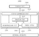
도 11은 본 발명의 기술적 사상의 일 실시예에 의한 전자 시스템(2300)을 개념적으로 도시한 블록다이어그램이다. 도 11을 참조하면, 본 발명의 일 실시예에 의한 전자 시스템(2300)은 바디(2310), 디스플레이 유닛(2360), 및 외부 장치(2370)를 포함할 수 있다. 상기 바디(2310)는 마이크로 프로세서 유닛(Micro Processor Unit; 2320), 파워 공급부(Power Supply; 2330), 기능 유닛(Function Unit; 2340), 및/또는 디스플레이 컨트롤 유닛(Display Control Unit; 2350)을 포함할 수 있다. 상기 바디(2310)는 인쇄 회로기판(PCB) 등을 갖는 시스템 보드 또는 마더 보드(Mother Board), 및/또는 케이스(case)를 포함할 수 있다. 상기 마이크로 프로세서 유닛(2320), 상기 파워 공급부(2330), 상기 기능 유닛(2340), 및 상기 디스플레이 컨트롤 유닛(2350)은 상기 바디(2310)의 상면 또는 내부에 실장 또는 배치될 수 있다. 상기 바디(2310)의 상면 혹은 상기 바디(2310)의 내/외부에 디스플레이 유닛(2360)이 배치될 수 있다. 상기 디스플레이 유닛(2360)은 디스플레이 컨트롤 유닛(2350)에 의해 프로세싱된 이미지를 표시할 수 있다. 예를 들어, 상기 디스플레이 유닛(2360)은 LCD (liquid crystal display), AMOLED(active matrix organic light emitting diodes), 또는 다양한 디스플레이 패널을 포함할 수 있다. 상기 디스플레이 유닛(2360)은 터치 스크린을 포함할 수 있다. 따라서, 상기 디스플레이 유닛(2360)은 입출력 기능을 가질 수 있다. 상기 파워 공급부(2330)는 전류 또는 전압을 상기 마이크로 프로세서 유닛(2320), 상기 기능 유닛(2340), 상기 디스플레이 컨트롤 유닛(2350) 등으로 공급할 수 있다. 상기 파워 공급부(2330)는 충전 배터리, 건전지용 소켓, 또는 전압/전류 변환기를 포함할 수 있다. 상기 마이크로 프로세서 유닛(2320)은 상기 파워 공급부(2330)로부터 전압을 공급받아 상기 기능 유닛(2340)과 상기 디스플레이 유닛(2360)을 제어할 수 있다. 예를 들어, 상기 마이크로 프로세서 유닛(2320)은 CPU 또는 AP (application processor)를 포함할 수 있다. 상기 기능 유닛(2340)은 터치 패드, 터치 스크린, 휘발성/비휘발성 메모리, 메모리 카드 컨트롤러, 카메라, 라이트, 음성 및 동영상 재생 프로세서, 무선 송수신 안테나, 스피커, 마이크, USB 포트, 기타 다양한 기능을 가진 유닛을 포함할 수 있다. 상기 마이크로 프로세서 유닛(2320) 또는 상기 기능 유닛(2340)은 본 발명의 기술적 사상의 다양한 실시예들에 의한 반도체 소자들(100A-100D) 중 적어도 하나를 포함할 수 있다.11 is a block diagram conceptually showing an
도 12를 참조하면, 본 발명의 일 실시예에 의한 전자 시스템(2400)은 버스(2420)를 통하여 데이터 통신을 수행하는 마이크로프로세서(2414), 메모리 시스템(2412) 및 유저 인터페이스(2418)를 포함할 수 있다. 상기 마이크로프로세서(2414)는 CPU 또는 AP를 포함할 수 있다. 상기 전자 시스템(2400)은 상기 마이크로프로세서(2414)와 직접적으로 통신하는 상기 램(2416)을 더 포함할 수 있다. 상기 마이크로프로세서(2414) 및/또는 상기 램(2416)은 단일 패키지 내에 조립될 수 있다. 상기 유저 인터페이스(2418)는 상기 전자 시스템(2400)으로 정보를 입력하거나 또는 상기 전자 시스템(2400)으로부터 정보를 출력하는데 사용될 수 있다. 예를 들어, 상기 유저 인터페이스(2418)는 터치 패드, 터치 스크린, 키보드, 마우스, 스캐너, 음성 디텍터, CRT(cathode ray tube) 모니터, LCD, AMOLED, PDP(plasma display panel), 프린터, 라이트, 또는 기타 다양한 입출력 장치들을 포함할 수 있다. 상기 메모리 시스템(2412)은 상기 마이크로프로세서(2414) 동작용 코드들, 상기 마이크로프로세서(2414)에 의해 처리된 데이터, 또는 외부 입력 데이터를 저장할 수 있다. 상기 메모리 시스템(2412)은 메모리 컨트롤러, 하드 디스크, 또는 SSD(solid state drive)를 포함할 수 있다. 상기 마이크로프로세서(2414), 상기 램(2416), 및/또는 상기 메모리 시스템(2412)은 본 발명의 기술적 사상의 다양한 실시예들에 의한 반도체 소자들(100A-100D) 중 적어도 하나를 포함할 수 있다.Referring to FIG. 12, an
이상, 첨부된 도면을 참조하여 본 발명의 실시 예를 설명하였지만, 본 발명이 속하는 기술분야에서 통상의 지식을 가진 자는 본 발명이 그 기술적 사상이나 필수적인 특징을 변경하지 않고서 다른 구체적인 형태로 실시될 수 있다는 것을 이해할 수 있을 것이다. 그러므로 이상에서 기술한 실시 예에는 모든 면에서 예시적인 것이며 한정적이 아닌 것으로 이해해야만 한다.In the above, embodiments of the present invention have been described with reference to the accompanying drawings, but those of ordinary skill in the art to which the present invention pertains can be implemented in other specific forms without changing the technical spirit or essential features. You can understand that there is. Therefore, it should be understood that the embodiments described above are illustrative in all respects and are not limiting.
100A-100F: 반도체 소자
10: 기판11: 활성 영역
11s: 소스 영역11d: 드레인 영역
12: 소자 분리 영역12a: 소자 분리 트렌치
12b: 소자 분리 절연물12L: 소자 분리 라인
20: 게이트 구조체21: 게이트 트렌치
22: 게이트 절연층23: 게이트 배리어 패턴
23a: 게이트 배리어 층24: 게이트 전극 패턴
24a: 게이트 전극층25: 전극 보호층
26: 버퍼 산화층27: 게이트 캡핑 절연층
31: 트렌치 마스크 층32: 하부 층간 절연층
33: 홀 마스크 층h: 홀
34: 스페이서 층35: 상부 층간 절연층
36: 식각 정지층37: 몰딩 산화물 층
38: 커패시터 캡핑 절연층40h: 비트 라인 컨택 홀
40: 비트 라인 컨택 플러그45: 보호 절연층
50: 비트 라인 구조체53: 비트 라인 배리어 패턴
53a: 비트 라인 배리어 층54: 비트 라인 전극 패턴
54a: 비트 라인 전극 층55: 비트 라인 캡핑 패턴
55a: 비트 라인 캡핑 층50L: 비트 라인
60h: 커패시터 컨택 홀60: 커패시터 컨택 플러그
80: 커패시터 구조체81h: 커패시터 전극 홀
81: 커패시터 하부 전극83: 커패시터 유전층
85: 커패시터 상부 전극100A-100F: Semiconductor device
10: substrate 11: active area
11s:
12:
12b:
20: gate structure 21: gate trench
22: gate insulating layer 23: gate barrier pattern
23a: gate barrier layer 24: gate electrode pattern
24a: gate electrode layer 25: electrode protective layer
26: buffer oxide layer 27: gate capping insulating layer
31: trench mask layer 32: lower interlayer insulating layer
33: hole mask layer h: hole
34: spacer layer 35: upper interlayer insulating layer
36: etch stop layer 37: molding oxide layer
38: capacitor capping insulating
40: bit line contact plug 45: protective insulating layer
50: bit line structure 53: bit line barrier pattern
53a: bit line barrier layer 54: bit line electrode pattern
54a: bit line electrode layer 55: bit line capping pattern
55a: bit
60h: capacitor contact hole 60: capacitor contact plug
80:
81: capacitor lower electrode 83: capacitor dielectric layer
85: capacitor upper electrode
Claims (10)
Translated fromKorean상기 기판 내의 상기 활성 영역 내에 매립된 게이트 구조체들을 포함하고;
상기 게이트 구조체들 중 적어도 하나는:
게이트 트렌치;
상기 게이트 트렌치의 내벽 상에 컨포멀하게 형성된 게이트 절연층;
상기 게이트 트렌치의 하부 영역의 상기 게이트 절연층 상에 컨포멀하게 형성된 게이트 배리어 패턴;
상기 게이트 배리어 패턴 상에 형성되고 상기 게이트 트렌치의 하부 영역을 채우는 게이트 전극 패턴;
상기 게이트 배리어 패턴 및 상기 게이트 전극 패턴과 접촉하도록 상기 게이트 트렌치의 상부 영역의 상기 게이트 절연층 상에 컨포멀하게 형성된 전극 보호층;
상기 전극 보호층 상에 컨포멀하게 형성된 버퍼 산화층; 및
상기 게이트 트렌치의 상부 영역을 채우도록 상기 버퍼 산화층 상에 형성된 게이트 캡핑 절연층을 포함하고,
상기 게이트 배리어 패턴의 상단부는 상기 게이트 전극 패턴의 상단부보다 낮게 리세스되고,
상기 전극 보호층의 일부는 상기 리세스된 게이트 배리어 패턴의 상단부 상의 상기 게이트 절연층과 상기 게이트 전극 패턴사이에 개재되는 반도체 소자.A device isolation region defining an active region in the substrate; And
Including gate structures buried in the active region in the substrate;
At least one of the gate structures is:
Gate trench;
A gate insulating layer conformally formed on the inner wall of the gate trench;
A gate barrier pattern conformally formed on the gate insulating layer in a lower region of the gate trench;
A gate electrode pattern formed on the gate barrier pattern and filling a lower region of the gate trench;
An electrode protection layer conformally formed on the gate insulating layer in an upper region of the gate trench to contact the gate barrier pattern and the gate electrode pattern;
A buffer oxide layer conformally formed on the electrode protective layer; And
A gate capping insulating layer formed on the buffer oxide layer to fill an upper region of the gate trench,
The upper end of the gate barrier pattern is recessed lower than the upper end of the gate electrode pattern,
A portion of the electrode protection layer is interposed between the gate insulating layer and the gate electrode pattern on an upper end of the recessed gate barrier pattern.
상기 전극 보호층은 실리콘 질화물을 포함하는 반도체 소자.The method of claim 1,
The electrode protective layer is a semiconductor device including silicon nitride.
상기 버퍼 산화층은 N형 불순물을 가진 실리콘 산화물을 포함하는 반도체 소자.The method of claim 1,
The buffer oxide layer includes a silicon oxide having an N-type impurity.
상기 게이트 구조체들 사이의 소스 영역을 더 포함하고,
상기 소스 영역은 상기 버퍼 산화층이 포함하는 N형 불순물과 동일한 도펀트를 포함하는 반도체 소자.The method of claim 3,
Further comprising a source region between the gate structures,
The source region includes a dopant identical to an N-type impurity included in the buffer oxide layer.
상기 게이트 캡핑 절연층은 실리콘 질화물을 포함하는 반도체 소자.The method of claim 1,
The gate capping insulating layer is a semiconductor device including silicon nitride.
상기 게이트 구조체들 사이의 상기 기판과 수직으로 정렬되도록 상기 기판 상에 형성된 비트 라인 컨택 플러그;
상기 비트 라인 컨택 플러그 상에 형성된 비트 라인 구조체; 및
상기 비트 라인 구조체를 덮는 스페이서 층을 포함하고,
상기 게이트 구조체들은 각각:
상기 기판 내에 형성된 게이트 트렌치;
상기 게이트 트렌치의 내벽 상에 컨포멀하게 형성된 게이트 절연층;
상기 게이트 트렌치의 하부 영역의 상기 게이트 절연층 상에 컨포멀하게 형성된 게이트 배리어 패턴;
상기 게이트 배리어 패턴 상에 형성되고 상기 게이트 트렌치의 하부 영역을 채우는 게이트 전극 패턴;
상기 게이트 트렌치의 상부 영역의 상기 게이트 절연층 상에 컨포멀하게 형성되는 실리콘 산화물 층; 및
상기 게이트 트렌치의 상부 영역을 채우도록 상기 실리콘 산화물 층 상에 형성된 실리콘 질화물 층을 포함하고,
상기 게이트 배리어 패턴의 상단부는 상기 게이트 전극 패턴의 상단부보다 낮게 리세스되어 상기 게이트 절연층과 상기 게이트 전극 패턴 사이에 갭이 형성되고,
상기 실리콘 산화물 층의 일부는 상기 갭 내에 채워지는 반도체 소자.Gate structures buried in the substrate;
A bit line contact plug formed on the substrate to be vertically aligned with the substrate between the gate structures;
A bit line structure formed on the bit line contact plug; And
Including a spacer layer covering the bit line structure,
Each of the gate structures:
A gate trench formed in the substrate;
A gate insulating layer conformally formed on the inner wall of the gate trench;
A gate barrier pattern conformally formed on the gate insulating layer in a lower region of the gate trench;
A gate electrode pattern formed on the gate barrier pattern and filling a lower region of the gate trench;
A silicon oxide layer conformally formed on the gate insulating layer in an upper region of the gate trench; And
A silicon nitride layer formed on the silicon oxide layer to fill an upper region of the gate trench,
The upper end of the gate barrier pattern is recessed lower than the upper end of the gate electrode pattern to form a gap between the gate insulating layer and the gate electrode pattern,
A portion of the silicon oxide layer is filled in the gap.
상기 실리콘 산화물 층은 인(P)을 포함하는 반도체 소자.The method of claim 8,
The silicon oxide layer includes phosphorus (P).
Priority Applications (4)
| Application Number | Priority Date | Filing Date | Title |
|---|---|---|---|
| KR1020140061198AKR102164542B1 (en) | 2014-05-21 | 2014-05-21 | Semiconductor Devices Having Buried Gate Structures and Methods of the Same |
| US14/551,857US9437697B2 (en) | 2014-05-21 | 2014-11-24 | Semiconductor device having buried gate structure and method of fabricating the same |
| US15/229,351US9893069B2 (en) | 2014-05-21 | 2016-08-05 | Semiconductor device having buried gate structure and method of fabricating the same |
| US15/865,467US10249628B2 (en) | 2014-05-21 | 2018-01-09 | Semiconductor device having buried gate structure and method of fabricating the same |
Applications Claiming Priority (1)
| Application Number | Priority Date | Filing Date | Title |
|---|---|---|---|
| KR1020140061198AKR102164542B1 (en) | 2014-05-21 | 2014-05-21 | Semiconductor Devices Having Buried Gate Structures and Methods of the Same |
Publications (2)
| Publication Number | Publication Date |
|---|---|
| KR20150134180A KR20150134180A (en) | 2015-12-01 |
| KR102164542B1true KR102164542B1 (en) | 2020-10-12 |
Family
ID=54556651
Family Applications (1)
| Application Number | Title | Priority Date | Filing Date |
|---|---|---|---|
| KR1020140061198AActiveKR102164542B1 (en) | 2014-05-21 | 2014-05-21 | Semiconductor Devices Having Buried Gate Structures and Methods of the Same |
Country Status (2)
| Country | Link |
|---|---|
| US (3) | US9437697B2 (en) |
| KR (1) | KR102164542B1 (en) |
Families Citing this family (34)
| Publication number | Priority date | Publication date | Assignee | Title |
|---|---|---|---|---|
| KR102164542B1 (en) | 2014-05-21 | 2020-10-12 | 삼성전자 주식회사 | Semiconductor Devices Having Buried Gate Structures and Methods of the Same |
| KR102316160B1 (en)* | 2014-12-22 | 2021-10-26 | 삼성전자주식회사 | Semiconductor device and method of manufacturing the same |
| US9515183B2 (en)* | 2015-03-11 | 2016-12-06 | Kabushiki Kaisha Toshiba | Semiconductor device including buried-gate MOS transistor with appropriate stress applied thereto |
| US10032873B2 (en)* | 2015-09-15 | 2018-07-24 | Taiwan Semiconductor Manufacturing Company, Ltd. | Semiconductor device and method of forming the same |
| DE102016113434B4 (en) | 2015-09-15 | 2020-11-19 | Taiwan Semiconductor Manufacturing Company, Ltd. | Semiconductor device and method of forming the same |
| KR102481478B1 (en)* | 2016-06-16 | 2022-12-26 | 삼성전자 주식회사 | Semiconductor devices and method of forming the same |
| KR102450577B1 (en)* | 2016-08-12 | 2022-10-11 | 삼성전자주식회사 | Semiconductor devices |
| KR102543181B1 (en)* | 2016-11-04 | 2023-06-15 | 삼성전자주식회사 | Semiconductor devices |
| CN108269805B (en)* | 2016-12-30 | 2021-06-08 | 联华电子股份有限公司 | Semiconductor memory device and method of making the same |
| CN108346666B (en) | 2017-01-23 | 2022-10-04 | 联华电子股份有限公司 | Semiconductor element and manufacturing method thereof |
| KR102222542B1 (en) | 2017-04-12 | 2021-03-05 | 삼성전자주식회사 | Semiconductor device and method for fabricating the same |
| KR20180129387A (en) | 2017-05-26 | 2018-12-05 | 에스케이하이닉스 주식회사 | Semiconductor device and method for fabricating the same |
| CN109037217B (en)* | 2017-06-09 | 2021-05-18 | 华邦电子股份有限公司 | memory device |
| KR102358460B1 (en)* | 2017-08-10 | 2022-02-07 | 삼성전자주식회사 | Semiconductor memory device and method of forming the same |
| KR102378471B1 (en)* | 2017-09-18 | 2022-03-25 | 삼성전자주식회사 | A semiconductor memory device and a method for manufacturing the same |
| TWI649838B (en)* | 2018-04-10 | 2019-02-01 | 華邦電子股份有限公司 | Semiconductor device and method of manufacturing same |
| CN110890369B (en)* | 2018-09-07 | 2024-05-21 | 长鑫存储技术有限公司 | Method for manufacturing semiconductor device and semiconductor device |
| US11152375B2 (en)* | 2019-01-28 | 2021-10-19 | Micron Technology, Inc. | Contact patterning |
| US10957699B2 (en)* | 2019-04-08 | 2021-03-23 | Micron Technology, Inc. | Integrated assemblies which include two different types of silicon nitride, and methods of forming integrated assemblies |
| TWI703565B (en)* | 2019-08-21 | 2020-09-01 | 華邦電子股份有限公司 | Memory device and manufacturing method thereof |
| CN111640746A (en)* | 2019-09-17 | 2020-09-08 | 福建省晋华集成电路有限公司 | Semiconductor device, forming method thereof and memory |
| CN113707610B (en)* | 2020-05-21 | 2023-04-18 | 长鑫存储技术有限公司 | Semiconductor device and method of forming the same |
| US11227926B2 (en)* | 2020-06-01 | 2022-01-18 | Nanya Technology Corporation | Semiconductor device and method for fabricating the same |
| KR20220014588A (en) | 2020-07-29 | 2022-02-07 | 삼성전자주식회사 | A semiconductor device |
| US11309214B2 (en)* | 2020-08-11 | 2022-04-19 | Nanya Technology Corporation | Semiconductor device with graphene-based element and method for fabricating the same |
| CN114121880B (en)* | 2020-08-27 | 2023-05-05 | 长鑫存储技术有限公司 | Semiconductor structure and manufacturing method thereof |
| US11469234B2 (en)* | 2020-11-13 | 2022-10-11 | Nanya Technology Corporation | Semiconductor device having reduced contact resistance between access transistors and conductive features and method of manufacturing the same |
| KR20220099142A (en) | 2021-01-04 | 2022-07-13 | 삼성전자주식회사 | Semiconductor memory device |
| US11812606B2 (en)* | 2021-03-05 | 2023-11-07 | Micron Technology, Inc. | Semiconductor device having gate trench |
| KR20230029190A (en) | 2021-08-24 | 2023-03-03 | 삼성전자주식회사 | Gate structures and semiconductor devices including the same |
| US12426252B2 (en)* | 2021-09-13 | 2025-09-23 | Changxin Memory Technologies, Inc. | Semiconductor structure comprising buried gate structure and isolation structure with air gap and method for manufacturing semiconductor structure |
| KR102614117B1 (en)* | 2021-11-05 | 2023-12-13 | 서울과학기술대학교 산학협력단 | Capacitor for semiconductor device, method of manufacturing capacitor for semiconductor device, and dram device |
| CN116113233B (en)* | 2021-11-09 | 2025-10-03 | 长鑫存储技术有限公司 | Buried bit line structure, method for preparing buried bit line structure, and memory |
| US20240407156A1 (en)* | 2023-06-02 | 2024-12-05 | Nanya Technology Corporation | Semiconductor memory device and manufacturing method thereof |
Citations (2)
| Publication number | Priority date | Publication date | Assignee | Title |
|---|---|---|---|---|
| US20140027813A1 (en)* | 2012-07-24 | 2014-01-30 | Marian Kuruc | Method of forming a semiconductor device having a patterned gate dielectric and structure therefor |
| US20140064004A1 (en)* | 2012-08-31 | 2014-03-06 | SK Hynix Inc. | Semiconductor device including buried gate, module and system, and method for manufacturing |
Family Cites Families (14)
| Publication number | Priority date | Publication date | Assignee | Title |
|---|---|---|---|---|
| KR20100096488A (en)* | 2009-02-24 | 2010-09-02 | 삼성전자주식회사 | Semiconductor device having recess channel structure |
| KR101060611B1 (en)* | 2009-07-03 | 2011-08-31 | 주식회사 하이닉스반도체 | Method of manufacturing semiconductor device with buried gate |
| KR101105433B1 (en) | 2009-07-03 | 2012-01-17 | 주식회사 하이닉스반도체 | Semiconductor device with buried gate and manufacturing method thereof |
| KR101670332B1 (en) | 2010-05-13 | 2016-10-31 | 에스케이하이닉스 주식회사 | Semiconductor device with buried gate and method for manufacturing the same |
| KR101749055B1 (en)* | 2010-10-06 | 2017-06-20 | 삼성전자주식회사 | A semiconductor device and a method of forming the same |
| KR101820022B1 (en) | 2010-11-11 | 2018-01-19 | 삼성전자주식회사 | Semiconductor devices having vertical channel transistors and methods for fabricating the same |
| KR101205143B1 (en) | 2010-11-15 | 2012-11-26 | 에스케이하이닉스 주식회사 | Semiconductor Device and Method for Manufacturing the same |
| WO2012144147A1 (en)* | 2011-04-20 | 2012-10-26 | パナソニック株式会社 | Vertical gate semiconductor device and method of manufacturing same |
| US8546885B2 (en)* | 2011-07-25 | 2013-10-01 | Taiwan Semiconductor Manufacturing Company, Ltd. | Metal gate electrode of a field effect transistor |
| KR101742817B1 (en)* | 2011-08-23 | 2017-06-02 | 삼성전자 주식회사 | Semiconductor device and method of manufacturing the same |
| JP6104523B2 (en)* | 2012-06-07 | 2017-03-29 | 株式会社日立製作所 | Manufacturing method of semiconductor device |
| KR20130142738A (en)* | 2012-06-20 | 2013-12-30 | 삼성전자주식회사 | Methods of fabricating semiconductor devices |
| US8710575B1 (en)* | 2013-01-31 | 2014-04-29 | Infineon Technologies Ag | Semiconductor device, integrated circuit and method of manufacturing an integrated circuit |
| KR102164542B1 (en) | 2014-05-21 | 2020-10-12 | 삼성전자 주식회사 | Semiconductor Devices Having Buried Gate Structures and Methods of the Same |
- 2014
- 2014-05-21KRKR1020140061198Apatent/KR102164542B1/enactiveActive
- 2014-11-24USUS14/551,857patent/US9437697B2/enactiveActive
- 2016
- 2016-08-05USUS15/229,351patent/US9893069B2/enactiveActive
- 2018
- 2018-01-09USUS15/865,467patent/US10249628B2/enactiveActive
Patent Citations (2)
| Publication number | Priority date | Publication date | Assignee | Title |
|---|---|---|---|---|
| US20140027813A1 (en)* | 2012-07-24 | 2014-01-30 | Marian Kuruc | Method of forming a semiconductor device having a patterned gate dielectric and structure therefor |
| US20140064004A1 (en)* | 2012-08-31 | 2014-03-06 | SK Hynix Inc. | Semiconductor device including buried gate, module and system, and method for manufacturing |
Also Published As
| Publication number | Publication date |
|---|---|
| US20180130805A1 (en) | 2018-05-10 |
| US20160343714A1 (en) | 2016-11-24 |
| US10249628B2 (en) | 2019-04-02 |
| US9893069B2 (en) | 2018-02-13 |
| KR20150134180A (en) | 2015-12-01 |
| US9437697B2 (en) | 2016-09-06 |
| US20150340453A1 (en) | 2015-11-26 |
Similar Documents
| Publication | Publication Date | Title |
|---|---|---|
| KR102164542B1 (en) | Semiconductor Devices Having Buried Gate Structures and Methods of the Same | |
| US11942515B2 (en) | Semiconductor device having asymmetrical source/drain | |
| US11784256B2 (en) | Semiconductor devices | |
| US10964794B2 (en) | Cryogenic semiconductor device having buried channel array transistor | |
| TWI523203B (en) | Semiconductor device and method for fabricating the same | |
| US9105494B2 (en) | Termination trench for power MOSFET applications | |
| CN103456694B (en) | Semiconductor devices and its manufacture method with air gap | |
| KR101934366B1 (en) | Semiconductor devices having recessed active regions and methods for fabricating the same | |
| US9406795B2 (en) | Trench gate MOSFET | |
| KR101868799B1 (en) | Nonvolatile memory device and method for fabricating the same | |
| KR102161800B1 (en) | Semiconductor devices and methods of manufacturing the same | |
| CN106057803B (en) | Semiconductor device having spacers on isolation regions | |
| US9786784B1 (en) | Vertical field effect transistor and method of fabricating the same | |
| KR102204387B1 (en) | Semiconductor device having buried gate structure and method of fabricating the same | |
| KR20150062768A (en) | Methods of Fabricating Semiconductor devices having Double-Layered Blocking Insulating Layers | |
| US8928073B2 (en) | Semiconductor devices including guard ring structures | |
| KR20160144164A (en) | Semiconductor device blocking a leakage current and method for fabricating the same | |
| CN107393960A (en) | Vertical field-effect transistor and its manufacture method | |
| JP2015005703A (en) | Semiconductor device and method of manufacturing the same | |
| KR102070094B1 (en) | Semiconductor Device Having a Resistor Electrode | |
| US20130210225A1 (en) | Method for fabricating semiconductor device | |
| KR20140112263A (en) | Memory device and method of manufacturing the same | |
| KR20220087892A (en) | Semiconductor device | |
| US20240162301A1 (en) | Semiconductor device and method for fabricating the same | |
| CN104716084B (en) | Method for manufacturing semiconductor element |
Legal Events
| Date | Code | Title | Description |
|---|---|---|---|
| PA0109 | Patent application | St.27 status event code:A-0-1-A10-A12-nap-PA0109 | |
| PG1501 | Laying open of application | St.27 status event code:A-1-1-Q10-Q12-nap-PG1501 | |
| R17-X000 | Change to representative recorded | St.27 status event code:A-3-3-R10-R17-oth-X000 | |
| R17-X000 | Change to representative recorded | St.27 status event code:A-3-3-R10-R17-oth-X000 | |
| PA0201 | Request for examination | St.27 status event code:A-1-2-D10-D11-exm-PA0201 | |
| E902 | Notification of reason for refusal | ||
| PE0902 | Notice of grounds for rejection | St.27 status event code:A-1-2-D10-D21-exm-PE0902 | |
| E13-X000 | Pre-grant limitation requested | St.27 status event code:A-2-3-E10-E13-lim-X000 | |
| P11-X000 | Amendment of application requested | St.27 status event code:A-2-2-P10-P11-nap-X000 | |
| P13-X000 | Application amended | St.27 status event code:A-2-2-P10-P13-nap-X000 | |
| E701 | Decision to grant or registration of patent right | ||
| PE0701 | Decision of registration | St.27 status event code:A-1-2-D10-D22-exm-PE0701 | |
| GRNT | Written decision to grant | ||
| PR0701 | Registration of establishment | St.27 status event code:A-2-4-F10-F11-exm-PR0701 | |
| PR1002 | Payment of registration fee | St.27 status event code:A-2-2-U10-U11-oth-PR1002 Fee payment year number:1 | |
| PG1601 | Publication of registration | St.27 status event code:A-4-4-Q10-Q13-nap-PG1601 | |
| PR1001 | Payment of annual fee | St.27 status event code:A-4-4-U10-U11-oth-PR1001 Fee payment year number:4 | |
| PR1001 | Payment of annual fee | St.27 status event code:A-4-4-U10-U11-oth-PR1001 Fee payment year number:5 | |
| P22-X000 | Classification modified | St.27 status event code:A-4-4-P10-P22-nap-X000 | |
| PR1001 | Payment of annual fee | St.27 status event code:A-4-4-U10-U11-oth-PR1001 Fee payment year number:6 |