KR102163358B1 - Display Device - Google Patents
Display DeviceDownload PDFInfo
- Publication number
- KR102163358B1 KR102163358B1KR1020140091725AKR20140091725AKR102163358B1KR 102163358 B1KR102163358 B1KR 102163358B1KR 1020140091725 AKR1020140091725 AKR 1020140091725AKR 20140091725 AKR20140091725 AKR 20140091725AKR 102163358 B1KR102163358 B1KR 102163358B1
- Authority
- KR
- South Korea
- Prior art keywords
- data
- display area
- pad
- substrate
- gate
- Prior art date
- Legal status (The legal status is an assumption and is not a legal conclusion. Google has not performed a legal analysis and makes no representation as to the accuracy of the status listed.)
- Active
Links
Images


Classifications
- H—ELECTRICITY
- H01—ELECTRIC ELEMENTS
- H01L—SEMICONDUCTOR DEVICES NOT COVERED BY CLASS H10
- H01L23/00—Details of semiconductor or other solid state devices
- H01L23/544—Marks applied to semiconductor devices or parts, e.g. registration marks, alignment structures, wafer maps
- G—PHYSICS
- G02—OPTICS
- G02F—OPTICAL DEVICES OR ARRANGEMENTS FOR THE CONTROL OF LIGHT BY MODIFICATION OF THE OPTICAL PROPERTIES OF THE MEDIA OF THE ELEMENTS INVOLVED THEREIN; NON-LINEAR OPTICS; FREQUENCY-CHANGING OF LIGHT; OPTICAL LOGIC ELEMENTS; OPTICAL ANALOGUE/DIGITAL CONVERTERS
- G02F1/00—Devices or arrangements for the control of the intensity, colour, phase, polarisation or direction of light arriving from an independent light source, e.g. switching, gating or modulating; Non-linear optics
- G02F1/01—Devices or arrangements for the control of the intensity, colour, phase, polarisation or direction of light arriving from an independent light source, e.g. switching, gating or modulating; Non-linear optics for the control of the intensity, phase, polarisation or colour
- G02F1/13—Devices or arrangements for the control of the intensity, colour, phase, polarisation or direction of light arriving from an independent light source, e.g. switching, gating or modulating; Non-linear optics for the control of the intensity, phase, polarisation or colour based on liquid crystals, e.g. single liquid crystal display cells
- G02F1/133—Constructional arrangements; Operation of liquid crystal cells; Circuit arrangements
- G02F1/1333—Constructional arrangements; Manufacturing methods
- G02F1/1345—Conductors connecting electrodes to cell terminals
- G02F1/13452—Conductors connecting driver circuitry and terminals of panels
- H—ELECTRICITY
- H05—ELECTRIC TECHNIQUES NOT OTHERWISE PROVIDED FOR
- H05K—PRINTED CIRCUITS; CASINGS OR CONSTRUCTIONAL DETAILS OF ELECTRIC APPARATUS; MANUFACTURE OF ASSEMBLAGES OF ELECTRICAL COMPONENTS
- H05K1/00—Printed circuits
- H05K1/02—Details
- H05K1/14—Structural association of two or more printed circuits
- H05K1/147—Structural association of two or more printed circuits at least one of the printed circuits being bent or folded, e.g. by using a flexible printed circuit
- H—ELECTRICITY
- H10—SEMICONDUCTOR DEVICES; ELECTRIC SOLID-STATE DEVICES NOT OTHERWISE PROVIDED FOR
- H10H—INORGANIC LIGHT-EMITTING SEMICONDUCTOR DEVICES HAVING POTENTIAL BARRIERS
- H10H20/00—Individual inorganic light-emitting semiconductor devices having potential barriers, e.g. light-emitting diodes [LED]
- H10H20/01—Manufacture or treatment
- H—ELECTRICITY
- H10—SEMICONDUCTOR DEVICES; ELECTRIC SOLID-STATE DEVICES NOT OTHERWISE PROVIDED FOR
- H10H—INORGANIC LIGHT-EMITTING SEMICONDUCTOR DEVICES HAVING POTENTIAL BARRIERS
- H10H20/00—Individual inorganic light-emitting semiconductor devices having potential barriers, e.g. light-emitting diodes [LED]
- H10H20/80—Constructional details
- H10H20/85—Packages
- H10H20/857—Interconnections, e.g. lead-frames, bond wires or solder balls
- H—ELECTRICITY
- H10—SEMICONDUCTOR DEVICES; ELECTRIC SOLID-STATE DEVICES NOT OTHERWISE PROVIDED FOR
- H10H—INORGANIC LIGHT-EMITTING SEMICONDUCTOR DEVICES HAVING POTENTIAL BARRIERS
- H10H29/00—Integrated devices, or assemblies of multiple devices, comprising at least one light-emitting semiconductor element covered by group H10H20/00
- H10H29/10—Integrated devices comprising at least one light-emitting semiconductor component covered by group H10H20/00
- H10H29/14—Integrated devices comprising at least one light-emitting semiconductor component covered by group H10H20/00 comprising multiple light-emitting semiconductor components
- H10H29/142—Two-dimensional arrangements, e.g. asymmetric LED layout
- G—PHYSICS
- G02—OPTICS
- G02F—OPTICAL DEVICES OR ARRANGEMENTS FOR THE CONTROL OF LIGHT BY MODIFICATION OF THE OPTICAL PROPERTIES OF THE MEDIA OF THE ELEMENTS INVOLVED THEREIN; NON-LINEAR OPTICS; FREQUENCY-CHANGING OF LIGHT; OPTICAL LOGIC ELEMENTS; OPTICAL ANALOGUE/DIGITAL CONVERTERS
- G02F1/00—Devices or arrangements for the control of the intensity, colour, phase, polarisation or direction of light arriving from an independent light source, e.g. switching, gating or modulating; Non-linear optics
- G02F1/01—Devices or arrangements for the control of the intensity, colour, phase, polarisation or direction of light arriving from an independent light source, e.g. switching, gating or modulating; Non-linear optics for the control of the intensity, phase, polarisation or colour
- G02F1/13—Devices or arrangements for the control of the intensity, colour, phase, polarisation or direction of light arriving from an independent light source, e.g. switching, gating or modulating; Non-linear optics for the control of the intensity, phase, polarisation or colour based on liquid crystals, e.g. single liquid crystal display cells
- G02F1/133—Constructional arrangements; Operation of liquid crystal cells; Circuit arrangements
- G02F1/1333—Constructional arrangements; Manufacturing methods
- G02F1/133388—Constructional arrangements; Manufacturing methods with constructional differences between the display region and the peripheral region
- G—PHYSICS
- G02—OPTICS
- G02F—OPTICAL DEVICES OR ARRANGEMENTS FOR THE CONTROL OF LIGHT BY MODIFICATION OF THE OPTICAL PROPERTIES OF THE MEDIA OF THE ELEMENTS INVOLVED THEREIN; NON-LINEAR OPTICS; FREQUENCY-CHANGING OF LIGHT; OPTICAL LOGIC ELEMENTS; OPTICAL ANALOGUE/DIGITAL CONVERTERS
- G02F1/00—Devices or arrangements for the control of the intensity, colour, phase, polarisation or direction of light arriving from an independent light source, e.g. switching, gating or modulating; Non-linear optics
- G02F1/01—Devices or arrangements for the control of the intensity, colour, phase, polarisation or direction of light arriving from an independent light source, e.g. switching, gating or modulating; Non-linear optics for the control of the intensity, phase, polarisation or colour
- G02F1/13—Devices or arrangements for the control of the intensity, colour, phase, polarisation or direction of light arriving from an independent light source, e.g. switching, gating or modulating; Non-linear optics for the control of the intensity, phase, polarisation or colour based on liquid crystals, e.g. single liquid crystal display cells
- G02F1/133—Constructional arrangements; Operation of liquid crystal cells; Circuit arrangements
- G02F1/1333—Constructional arrangements; Manufacturing methods
- G02F1/1345—Conductors connecting electrodes to cell terminals
- G02F1/13458—Terminal pads
- G—PHYSICS
- G02—OPTICS
- G02F—OPTICAL DEVICES OR ARRANGEMENTS FOR THE CONTROL OF LIGHT BY MODIFICATION OF THE OPTICAL PROPERTIES OF THE MEDIA OF THE ELEMENTS INVOLVED THEREIN; NON-LINEAR OPTICS; FREQUENCY-CHANGING OF LIGHT; OPTICAL LOGIC ELEMENTS; OPTICAL ANALOGUE/DIGITAL CONVERTERS
- G02F1/00—Devices or arrangements for the control of the intensity, colour, phase, polarisation or direction of light arriving from an independent light source, e.g. switching, gating or modulating; Non-linear optics
- G02F1/01—Devices or arrangements for the control of the intensity, colour, phase, polarisation or direction of light arriving from an independent light source, e.g. switching, gating or modulating; Non-linear optics for the control of the intensity, phase, polarisation or colour
- G02F1/13—Devices or arrangements for the control of the intensity, colour, phase, polarisation or direction of light arriving from an independent light source, e.g. switching, gating or modulating; Non-linear optics for the control of the intensity, phase, polarisation or colour based on liquid crystals, e.g. single liquid crystal display cells
- G02F1/133—Constructional arrangements; Operation of liquid crystal cells; Circuit arrangements
- G02F1/136—Liquid crystal cells structurally associated with a semi-conducting layer or substrate, e.g. cells forming part of an integrated circuit
- G02F1/1362—Active matrix addressed cells
- G02F1/136286—Wiring, e.g. gate line, drain line
- H—ELECTRICITY
- H01—ELECTRIC ELEMENTS
- H01L—SEMICONDUCTOR DEVICES NOT COVERED BY CLASS H10
- H01L2223/00—Details relating to semiconductor or other solid state devices covered by the group H01L23/00
- H01L2223/544—Marks applied to semiconductor devices or parts
- H01L2223/5442—Marks applied to semiconductor devices or parts comprising non digital, non alphanumeric information, e.g. symbols
- H—ELECTRICITY
- H01—ELECTRIC ELEMENTS
- H01L—SEMICONDUCTOR DEVICES NOT COVERED BY CLASS H10
- H01L2223/00—Details relating to semiconductor or other solid state devices covered by the group H01L23/00
- H01L2223/544—Marks applied to semiconductor devices or parts
- H01L2223/54426—Marks applied to semiconductor devices or parts for alignment
- H—ELECTRICITY
- H01—ELECTRIC ELEMENTS
- H01L—SEMICONDUCTOR DEVICES NOT COVERED BY CLASS H10
- H01L2223/00—Details relating to semiconductor or other solid state devices covered by the group H01L23/00
- H01L2223/544—Marks applied to semiconductor devices or parts
- H01L2223/54473—Marks applied to semiconductor devices or parts for use after dicing
- H01L2223/54486—Located on package parts, e.g. encapsulation, leads, package substrate
- H—ELECTRICITY
- H01—ELECTRIC ELEMENTS
- H01L—SEMICONDUCTOR DEVICES NOT COVERED BY CLASS H10
- H01L23/00—Details of semiconductor or other solid state devices
- H01L23/52—Arrangements for conducting electric current within the device in operation from one component to another, i.e. interconnections, e.g. wires, lead frames
- H01L23/538—Arrangements for conducting electric current within the device in operation from one component to another, i.e. interconnections, e.g. wires, lead frames the interconnection structure between a plurality of semiconductor chips being formed on, or in, insulating substrates
- H01L23/5389—Arrangements for conducting electric current within the device in operation from one component to another, i.e. interconnections, e.g. wires, lead frames the interconnection structure between a plurality of semiconductor chips being formed on, or in, insulating substrates the chips being integrally enclosed by the interconnect and support structures
- H—ELECTRICITY
- H01—ELECTRIC ELEMENTS
- H01L—SEMICONDUCTOR DEVICES NOT COVERED BY CLASS H10
- H01L2924/00—Indexing scheme for arrangements or methods for connecting or disconnecting semiconductor or solid-state bodies as covered by H01L24/00
- H01L2924/0001—Technical content checked by a classifier
- H01L2924/0002—Not covered by any one of groups H01L24/00, H01L24/00 and H01L2224/00
- H—ELECTRICITY
- H05—ELECTRIC TECHNIQUES NOT OTHERWISE PROVIDED FOR
- H05K—PRINTED CIRCUITS; CASINGS OR CONSTRUCTIONAL DETAILS OF ELECTRIC APPARATUS; MANUFACTURE OF ASSEMBLAGES OF ELECTRICAL COMPONENTS
- H05K1/00—Printed circuits
- H05K1/02—Details
- H05K1/0266—Marks, test patterns or identification means
- H05K1/0269—Marks, test patterns or identification means for visual or optical inspection
- H—ELECTRICITY
- H05—ELECTRIC TECHNIQUES NOT OTHERWISE PROVIDED FOR
- H05K—PRINTED CIRCUITS; CASINGS OR CONSTRUCTIONAL DETAILS OF ELECTRIC APPARATUS; MANUFACTURE OF ASSEMBLAGES OF ELECTRICAL COMPONENTS
- H05K1/00—Printed circuits
- H05K1/18—Printed circuits structurally associated with non-printed electric components
- H05K1/189—Printed circuits structurally associated with non-printed electric components characterised by the use of a flexible or folded printed circuit
- H—ELECTRICITY
- H05—ELECTRIC TECHNIQUES NOT OTHERWISE PROVIDED FOR
- H05K—PRINTED CIRCUITS; CASINGS OR CONSTRUCTIONAL DETAILS OF ELECTRIC APPARATUS; MANUFACTURE OF ASSEMBLAGES OF ELECTRICAL COMPONENTS
- H05K2201/00—Indexing scheme relating to printed circuits covered by H05K1/00
- H05K2201/09—Shape and layout
- H05K2201/09818—Shape or layout details not covered by a single group of H05K2201/09009 - H05K2201/09809
- H05K2201/09918—Optically detected marks used for aligning tool relative to the PCB, e.g. for mounting of components
- H—ELECTRICITY
- H05—ELECTRIC TECHNIQUES NOT OTHERWISE PROVIDED FOR
- H05K—PRINTED CIRCUITS; CASINGS OR CONSTRUCTIONAL DETAILS OF ELECTRIC APPARATUS; MANUFACTURE OF ASSEMBLAGES OF ELECTRICAL COMPONENTS
- H05K2201/00—Indexing scheme relating to printed circuits covered by H05K1/00
- H05K2201/10—Details of components or other objects attached to or integrated in a printed circuit board
- H05K2201/10007—Types of components
- H05K2201/10128—Display
- H—ELECTRICITY
- H05—ELECTRIC TECHNIQUES NOT OTHERWISE PROVIDED FOR
- H05K—PRINTED CIRCUITS; CASINGS OR CONSTRUCTIONAL DETAILS OF ELECTRIC APPARATUS; MANUFACTURE OF ASSEMBLAGES OF ELECTRICAL COMPONENTS
- H05K2201/00—Indexing scheme relating to printed circuits covered by H05K1/00
- H05K2201/10—Details of components or other objects attached to or integrated in a printed circuit board
- H05K2201/10613—Details of electrical connections of non-printed components, e.g. special leads
- H05K2201/10621—Components characterised by their electrical contacts
- H05K2201/10681—Tape Carrier Package [TCP]; Flexible sheet connector
- H—ELECTRICITY
- H05—ELECTRIC TECHNIQUES NOT OTHERWISE PROVIDED FOR
- H05K—PRINTED CIRCUITS; CASINGS OR CONSTRUCTIONAL DETAILS OF ELECTRIC APPARATUS; MANUFACTURE OF ASSEMBLAGES OF ELECTRICAL COMPONENTS
- H05K3/00—Apparatus or processes for manufacturing printed circuits
- H05K3/36—Assembling printed circuits with other printed circuits
- H05K3/361—Assembling flexible printed circuits with other printed circuits
- H—ELECTRICITY
- H10—SEMICONDUCTOR DEVICES; ELECTRIC SOLID-STATE DEVICES NOT OTHERWISE PROVIDED FOR
- H10H—INORGANIC LIGHT-EMITTING SEMICONDUCTOR DEVICES HAVING POTENTIAL BARRIERS
- H10H20/00—Individual inorganic light-emitting semiconductor devices having potential barriers, e.g. light-emitting diodes [LED]
- H10H20/01—Manufacture or treatment
- H10H20/032—Manufacture or treatment of electrodes
- H—ELECTRICITY
- H10—SEMICONDUCTOR DEVICES; ELECTRIC SOLID-STATE DEVICES NOT OTHERWISE PROVIDED FOR
- H10H—INORGANIC LIGHT-EMITTING SEMICONDUCTOR DEVICES HAVING POTENTIAL BARRIERS
- H10H20/00—Individual inorganic light-emitting semiconductor devices having potential barriers, e.g. light-emitting diodes [LED]
- H10H20/01—Manufacture or treatment
- H10H20/036—Manufacture or treatment of packages
- H10H20/0364—Manufacture or treatment of packages of interconnections
- H—ELECTRICITY
- H10—SEMICONDUCTOR DEVICES; ELECTRIC SOLID-STATE DEVICES NOT OTHERWISE PROVIDED FOR
- H10K—ORGANIC ELECTRIC SOLID-STATE DEVICES
- H10K59/00—Integrated devices, or assemblies of multiple devices, comprising at least one organic light-emitting element covered by group H10K50/00
- H10K59/10—OLED displays
- H10K59/12—Active-matrix OLED [AMOLED] displays
- H10K59/131—Interconnections, e.g. wiring lines or terminals
Landscapes
- Physics & Mathematics (AREA)
- Microelectronics & Electronic Packaging (AREA)
- General Physics & Mathematics (AREA)
- Engineering & Computer Science (AREA)
- Nonlinear Science (AREA)
- Power Engineering (AREA)
- Computer Hardware Design (AREA)
- Condensed Matter Physics & Semiconductors (AREA)
- Crystallography & Structural Chemistry (AREA)
- Optics & Photonics (AREA)
- Chemical & Material Sciences (AREA)
- Mathematical Physics (AREA)
- Devices For Indicating Variable Information By Combining Individual Elements (AREA)
- Electroluminescent Light Sources (AREA)
Abstract
Translated fromKoreanDescription
Translated fromKorean본 발명은 디스플레이 장치에 관한 것으로서, 보다 구체적으로는 신호 패드에 신호 구동부를 접속하기 위해서 신호 패드와 신호 구동부 사이의 얼라인(align) 구조에 관한 것이다.The present invention relates to a display device, and more particularly, to an alignment structure between a signal pad and a signal driver to connect the signal driver to the signal pad.
초창기 디스플레이 장치인 음극선관(Cathode Ray Tube)을 대체하는 디스플레이 장치로서, 액정 표시 장치(Liquid Crystal Display Device), 플라즈마 디스플레이 패널(Plasma Display Panel), 및 유기 발광 표시 장치(Organic Light Emitting Display Device) 등이 개발된 바 있다.As a display device replacing the cathode ray tube, which is an early display device, a liquid crystal display device, a plasma display panel, an organic light emitting display device, etc. Has been developed.
이와 같은 디스플레이 장치는 무게와 부피를 줄임으로써 장치의 대형화를 가능하게 하였고, 응답속도나 화질 등에 있어서도 연구개발을 지속적으로 진행하여 현재 품질 면에서 많은 발전이 이루어졌다.Such a display device has made it possible to increase the size of the device by reducing the weight and volume, and a lot of progress has been made in terms of quality by continuing research and development in response speed and image quality.
최근에는 이와 같은 기술적인 면에서의 연구개발 이외에 수요자에게 어필할 수 있는 제품의 디자인적인 면에서의 연구개발이 진행되고 있고, 그 일환으로 상부 케이스(upper case)를 제거함으로써 화상을 디스플레이하는 표시 면에 별도의 케이스가 노출되지 않도록 한 보더리스(borderless) 디스플레이가 제안된 바 있다. 이와 같은 보더리스 디스플레이는 디자인의 미감이 증진되어 수요자의 구매요구에 부응할 수 있지만, 제조시 발생하는 다양한 문제들을 해결해야 하는 과제가 남아있다.Recently, in addition to research and development in the technical aspect, research and development in the design aspect of the product that can appeal to the consumer is in progress, and as part of that, the display surface that displays images by removing the upper case A borderless display has been proposed in which a separate case is not exposed to. Such a borderless display can meet the purchase demands of consumers by improving the aesthetics of the design, but there remains a task to solve various problems that occur during manufacturing.
이하, 도면을 참조로 종래의 디스플레이 장치에 대해서 설명하기로 한다.Hereinafter, a conventional display device will be described with reference to the drawings.
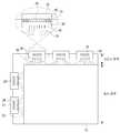
도 1은 종래의 디스플레이 장치의 개략적인 평면도이다.1 is a schematic plan view of a conventional display device.
도 1에서 알 수 있듯이, 종래의 디스플레이 장치는 기판(10), 게이트 구동부(20), 및 데이터 구동부(30)를 포함하여 이루어진다.As can be seen from FIG. 1, a conventional display device includes a
상기 기판(10)은 화상을 표시하는 표시 영역 및 화상을 표시하지 않는 비표시 영역으로 이루어진다. 상기 비표시 영역은 상기 표시 영역의 외곽에 형성된다.The
상기 표시 영역 내에는 복수의 화소가 형성된다. 상기 복수의 화소 각각은 게이트 배선, 데이터 배선, 및 박막 트랜지스터를 포함하여 이루어지고, 각각의 화소에서는 소정 파장의 광이 방출된다.A plurality of pixels are formed in the display area. Each of the plurality of pixels includes a gate line, a data line, and a thin film transistor, and each pixel emits light of a predetermined wavelength.
상기 게이트 구동부(20)는 상기 기판(10)의 제1 측면, 예로서 상기 기판(10)의 좌측 비표시 영역에 부착되어 있다. 상기 게이트 구동부(20)는 상기 게이트 배선에 게이트 신호를 공급한다. 이를 위해서, 상기 게이트 구동부(20)는 상기 기판(10)의 좌측 비표시 영역에 형성된 게이트 패드(26)와 전기적으로 연결되어 있고, 상기 게이트 패드(26)는 게이트 링크(25)를 통해서 상기 게이트 배선과 연결되어 있다.The
이와 같은 게이트 구동부(20)는 상기 게이트 패드(26)와 접속하는 연성 인쇄 회로 필름(flexible printed circuit film) 및 상기 연성 인쇄 회로 필름에 실장된 게이트 구동 집적 회로(21)를 포함하여 이루어진다. 상기 게이트 구동 집적 회로(21)는 게이트 신호를 생성하고 생성한 게이트 신호를 연성 인쇄 회로 필름을 통해 상기 게이트 패드(26)로 공급한다.The
상기 데이터 구동부(30)는 상기 기판(10)의 제2 측면, 예로서 상기 기판(10)의 상측 비표시 영역에 형성되어 있다. 상기 데이터 구동부(30)는 상기 데이터 배선에 데이터 신호를 공급한다. 이를 위해서, 상기 데이터 구동부(30)는 상기 기판(10)의 상측 비표시 영역에 형성된 데이터 패드(36)와 전기적으로 연결되어 있고, 상기 데이터 패드(36)는 데이터 링크(35)를 통해서 상기 데이터 배선과 연결되어 있다.The
이와 같은 데이터 구동부(30)는 상기 데이터 패드(36)와 접속하는 연성 인쇄 회로 필름(flexible printed circuit film) 및 상기 연성 인쇄 회로 필름에 실장된 데이터 구동 집적 회로(31)를 포함하여 이루어진다. 상기 데이터 구동 집적 회로(31)는 데이터 신호를 생성하고 생성한 데이터 신호를 연성 인쇄 회로 필름을 통해 상기 데이터 패드(36)로 공급한다.The
한편, 상기 게이트 패드(26)에 상기 게이트 구동부(20)를 접속하기 위해서는 상기 게이트 패드(26)와 상기 게이트 구동부(20)를 얼라인하는 공정을 수행하게 된다. 또한, 상기 데이터 패드(36)에 상기 데이터 구동부(30)를 접속하기 위해서는 상기 데이터 패드(36)와 상기 데이터 구동부(30)를 얼라인하는 공정을 수행하게 된다.Meanwhile, in order to connect the
도 1의 확대도에는 편의상 상기 데이터 패드(36)와 상기 데이터 구동부(30)를 얼라인하기 위한 구성요소만을 도시하였다.In the enlarged view of FIG. 1, only components for aligning the
도 1의 확대도에서 알 수 있듯이, 상기 데이터 패드(36)와 상기 데이터 구동부(30) 사이의 얼라인 공정은 제1 얼라인 마크(40)와 제2 얼라인 마크(50)를 이용하여 수행한다.As can be seen from the enlarged view of FIG. 1, the alignment process between the
상기 제1 얼라인 마크(40)는 상기 데이터 구동부(30) 상에, 보다 구체적으로는 상기 데이트 구동부(30)를 구성하는 연성 인쇄 회로 필름 상에 형성되어 있다.The
상기 제2 얼라인 마크(50)는 상기 기판(10) 상에, 보다 구체적으로는 상기 기판(10)의 상측 비표시 영역 상에 형성되어 있다.The
상기 제1 얼라인 마크(40)는 상기 제2 얼라인 마크(50)를 수용할 수 있는 수용홈을 구비하고 있고, 상기 제2 얼라인 마크(50)는 상기 수용홈에 수용될 수 있는 사각형 구조로 형성되어 있다.The
따라서, 상기 기판(10) 상에 형성된 제2 얼라인 마크(50)가 상기 데이터 구동부(30) 상에 형성된 제1 얼라인 마크(40)의 수용홈에 수용되도록 얼라인 공정을 수행하게 되며, 그와 같은 상태에서 상기 데이터 구동부(30)와 상기 데이터 패드(36)를 접속시키게 된다.Accordingly, an alignment process is performed so that the
도 2a 및 도 2b는 종래의 디스플레이 장치에서 데이터 구동부를 데이터 패드에 얼라인하는 공정을 도시한 공정도로서, 이는 전술한 도 1에 따른 디스플레이 장치에 관한 것이다. 따라서, 동일한 구성에 대해서는 동일한 도면부호를 부여하였다.2A and 2B are process diagrams illustrating a process of aligning a data driver with a data pad in a conventional display device, which relates to the display device of FIG. 1 described above. Accordingly, the same reference numerals are assigned to the same configuration.
우선, 도 2a에서 알 수 있듯이, 데이터 구동부(30)를 기판(10)의 상측으로 이동하면서 상기 기판(10)에 형성된 제2 얼라인 마크(50)가 상기 데이터 구동부(30)에 형성된 제1 얼라인 마크(40)의 수용홈 내에 수용되도록 상기 데이터 구동부(30)의 위치를 조정한다.First, as can be seen from FIG. 2A, a
그 후, 도 2b에서 알 수 있듯이, 상기 제2 얼라인 마크(50)가 상기 제1 얼라인 마크(40)의 수용홈 내에 수용된 상태로 상기 데이터 구동부(30)를 하강하여 상기 데이터 구동부(30)와 상기 기판(10) 상에 형성된 데이터 패드(36)와의 얼라인 공정을 완료한다.Thereafter, as can be seen in FIG. 2B, the
이상 설명한 바와 같이, 종래에는 데이터 구동부(30) 상에 형성되며 수용홈를 구비한 제1 얼라인 마크(40) 및 기판(10) 상에 형성되며 상기 수용홈에 수용될 수 있는 제2 얼라인 마크(50)를 이용하여 데이터 구동부(30)와 데이터 패드(36)의 얼라인 공정을 수행하였는데, 이 경우 상기 제1 얼라인 마크(40)가 디스플레이 장치의 표시 면에서 인식되는 문제가 있다.As described above, conventionally, a
특히, 종래의 경우 상기 데이터 구동부(30)에 형성된 제1 얼라인 마크(40)가 수용홈을 구비해야 하기 때문에 그 크기를 줄이는데 한계가 있고 그에 따라 표시 면에서 인식되는 제1 얼라인 마크(40)의 크기가 상당하여 시인성이 떨어지게 되며, 그에 따라 미감을 중요시하는 보더리스 디스플레이에는 적용되기 힘든 문제가 있다.In particular, in the conventional case, since the
본 발명은 전술한 종래의 문제점을 해결하기 위해 고안된 것으로서, 본 발명은 데이터 구동부에 형성된 얼라인 마크가 표시 면에서 인식되는 문제를 최소화할 수 있는 디스플레이 장치를 제공하는 것을 목적으로 한다.The present invention has been devised to solve the above-described conventional problem, and an object of the present invention is to provide a display device capable of minimizing the problem of recognizing an alignment mark formed in a data driver on a display surface.
본 발명은 상기 목적을 달성하기 위해서, 표시 영역 및 상기 표시 영역 외곽의 비표시 영역을 구비한 기판; 상기 기판의 표시 영역에 형성된 전극; 상기 기판의 비표시 영역에 형성되며, 상기 전극과 전기적으로 연결된 콘택 패드; 상기 기판의 비표시 영역에 형성된 신호 패드; 및 상기 기판의 비표시 영역에 형성되며, 상기 신호 패드와 연결된 신호 구동부를 포함하여 이루어지고, 상기 콘택 패드는 그 내부에 수용홈을 구비하고 있고, 상기 신호 구동부는 상기 수용홈에 수용되는 얼라인 마크를 구비하고 있는 디스플레이 장치를 제공한다.In order to achieve the above object, the present invention includes: a substrate having a display area and a non-display area outside the display area; An electrode formed in the display area of the substrate; A contact pad formed in a non-display area of the substrate and electrically connected to the electrode; A signal pad formed in a non-display area of the substrate; And a signal driver formed in a non-display area of the substrate and connected to the signal pad, wherein the contact pad has an accommodating groove therein, and the signal driver is aligned with the accommodating groove. A display device having a mark is provided.
이상과 같은 본 발명에 따르면 다음과 같은 효과가 있다.According to the present invention as described above has the following effects.
본 발명의 일 실시예에 따르면, 신호 구동부에 형성된 얼라인 마크에 수용홈을 형성할 필요가 없기 때문에 얼라인 마크의 크기를 줄일 수 있어 디스플레이 장치의 표시 면에서 인식되는 얼라인 마크의 크기를 최소화하여 시인성이 향상될 수 있다.According to an embodiment of the present invention, since it is not necessary to form an accommodation groove in the alignment mark formed in the signal driver, the size of the alignment mark can be reduced, thereby minimizing the size of the alignment mark recognized on the display surface of the display device. Thus, visibility can be improved.
도 1은 종래의 디스플레이 장치의 개략적인 평면도이다.
도 2a 및 도 2b는 종래의 디스플레이 장치에서 데이터 구동부를 데이터 패드에 얼라인하는 공정을 도시한 공정도이다.
도 3은 본 발명의 일 실시예에 따른 디스플레이 장치의 개략적인 평면도이다.
도 4a 및 도 4b는 본 발명의 일 실시예에 따른 디스플레이 장치에서 데이터 구동부를 데이터 패드에 얼라인하는 공정을 도시한 공정도이다.1 is a schematic plan view of a conventional display device.
2A and 2B are process diagrams illustrating a process of aligning a data driver with a data pad in a conventional display device.
3 is a schematic plan view of a display device according to an embodiment of the present invention.
4A and 4B are process diagrams illustrating a process of aligning a data driver with a data pad in a display device according to an exemplary embodiment of the present invention.
본 발명의 이점 및 특징, 그리고 그것들을 달성하는 방법은 첨부되는 도면과 함께 상세하게 후술되어 있는 실시예들을 참조하면 명확해질 것이다. 그러나 본 발명은 이하에서 개시되는 실시예들에 한정되는 것이 아니라 서로 다른 다양한 형태로 구현될 것이며, 단지 본 실시예들은 본 발명의 개시가 완전하도록 하며, 본 발명이 속하는 기술 분야에서 통상의 지식을 가진 자에게 발명의 범주를 완전하게 알려주기 위해 제공되는 것이며, 본 발명은 청구항의 범주에 의해 정의될 뿐이다.Advantages and features of the present invention, and a method of achieving them will become apparent with reference to the embodiments described below in detail together with the accompanying drawings. However, the present invention is not limited to the embodiments disclosed below, but will be implemented in various forms different from each other, and only these embodiments make the disclosure of the present invention complete, and common knowledge in the technical field to which the present invention pertains. It is provided to completely inform the scope of the invention to those who have it, and the invention is only defined by the scope of the claims.
본 발명의 실시예를 설명하기 위한 도면에 개시된 형상, 크기, 비율, 각도, 개수 등은 예시적인 것이므로 본 발명이 도시된 사항에 한정되는 것은 아니다. 명세서 전체에 걸쳐 동일 참조 부호는 동일 구성 요소를 지칭한다. 또한, 본 발명을 설명함에 있어서, 관련된 공지 기술에 대한 구체적인 설명이 본 발명의 요지를 불필요하게 흐릴 수 있다고 판단되는 경우 그 상세한 설명은 생략한다. 본 명세서 상에서 언급한 '포함한다', '갖는다', '이루어진다' 등이 사용되는 경우 '~만'이 사용되지 않는 이상 다른 부분이 추가될 수 있다. 구성 요소를 단수로 표현한 경우에 특별히 명시적인 기재 사항이 없는 한 복수를 포함하는 경우를 포함한다.The shapes, sizes, ratios, angles, numbers, etc. disclosed in the drawings for explaining the embodiments of the present invention are exemplary, and the present invention is not limited to the illustrated matters. The same reference numerals refer to the same components throughout the specification. In addition, in describing the present invention, when it is determined that a detailed description of related known technologies may unnecessarily obscure the subject matter of the present invention, the detailed description thereof will be omitted. When'include','have','consists of' and the like mentioned in the present specification are used, other parts may be added unless'only' is used. In the case of expressing the constituent elements in the singular, it includes the case of including the plural unless specifically stated otherwise.
구성 요소를 해석함에 있어서, 별도의 명시적 기재가 없더라도 오차 범위를 포함하는 것으로 해석한다.In interpreting the constituent elements, it is interpreted as including an error range even if there is no explicit description.
위치 관계에 대한 설명일 경우, 예를 들어, '~상에', '~상부에', '~하부에', '~옆에' 등으로 두 부분의 위치 관계가 설명되는 경우, '바로' 또는 '직접'이 사용되지 않는 이상 두 부분 사이에 하나 이상의 다른 부분이 위치할 수도 있다.In the case of a description of the positional relationship, for example, if the positional relationship of two parts is described as'upper','upper of','lower of','next to','right' Or, unless'direct' is used, one or more other parts may be located between the two parts.
시간 관계에 대한 설명일 경우, 예를 들어, '~후에', '~에 이어서', '~다음에', '~전에' 등으로 시간적 선후 관계가 설명되는 경우, '바로' 또는 '직접'이 사용되지 않는 이상 연속적이지 않은 경우도 포함할 수 있다.In the case of a description of a temporal relationship, for example, when a temporal predecessor relationship is described as'after','following','after','before', etc.,'right' or'direct' It may also include cases that are not continuous unless this is used.
제1, 제2 등이 다양한 구성요소들을 서술하기 위해서 사용되나, 이들 구성요소들은 이들 용어에 의해 제한되지 않는다. 이들 용어들은 단지 하나의 구성 요소를 다른 구성요소와 구별하기 위하여 사용하는 것이다. 따라서, 이하에서 언급되는 제1 구성요소는 본 발명의 기술적 사상 내에서 제2 구성요소일 수도 있다.First, second, etc. are used to describe various elements, but these elements are not limited by these terms. These terms are only used to distinguish one component from another component. Accordingly, the first component mentioned below may be a second component within the technical idea of the present invention.
본 발명의 여러 실시예들의 각각 특징들이 부분적으로 또는 전체적으로 서로 결합 또는 조합 가능하고, 기술적으로 다양한 연동 및 구동이 가능하며, 각 실시예들이 서로에 대하여 독립적으로 실시 가능할 수도 있고 연관 관계로 함께 실시할 수도 있다.Each of the features of the various embodiments of the present invention can be partially or entirely combined or combined with each other, technically various interlocking and driving are possible, and each of the embodiments can be implemented independently of each other or can be implemented together in a related relationship. May be.
이하, 도면을 참조로 본 발명의 바람직한 실시예에 대해서 상세히 설명하기로 한다.Hereinafter, a preferred embodiment of the present invention will be described in detail with reference to the drawings.
도 3은 본 발명의 일 실시예에 따른 디스플레이 장치의 개략적인 평면도로서, 이는 유기 발광 표시장치에 관한 것이다.3 is a schematic plan view of a display device according to an embodiment of the present invention, which relates to an organic light emitting display device.
도 3에서 알 수 있듯이, 본 발명의 일 실시예에 따른 디스플레이 장치는 기판(100), 게이트 구동부(200), 및 데이터 구동부(300)를 포함하여 이루어진다.As can be seen from FIG. 3, a display device according to an exemplary embodiment of the present invention includes a
상기 기판(100)은 화상을 표시하는 표시 영역 및 화상을 표시하지 않는 비표시 영역으로 이루어진다. 상기 표시 영역은 상기 기판(100)의 중앙부에 형성되고, 상기 비표시 영역은 상기 표시 영역의 외곽에 형성된다.The
상기 기판(100)의 표시 영역 내에는 복수의 화소(P)가 형성된다. 상기 복수의 화소(P) 각각은 게이트 배선(110), 데이터 배선(120), 고전위 전원 배선(130), 스위칭 박막 트랜지스터(T1), 구동 박막 트랜지스터(T2), 커패시터(C), 제1 전극(140), 제2 전극(150), 및 발광 다이오드(E)를 포함하여 이루어진다.A plurality of pixels P are formed in the display area of the
상기 게이트 배선(110)은 상기 게이트 구동부(200)에서 공급되는 게이트 신호를 상기 스위칭 박막 트랜지스터(T1)에 공급한다.The
상기 데이터 배선(120)은 상기 데이터 구동부(300)에서 공급되는 데이터 신호를 상기 스위칭 박막 트랜지스터(T1)에 공급한다.The
상기 고전위 전원 배선(130)은 상기 데이터 구동부(300)를 경유하여 공급되는 고전위 전압을 상기 구동 박막 트랜지스터(T2)에 공급한다.The high
상기 스위칭 박막 트랜지스터(T1)는 상기 게이트 배선(110)에 공급되는 게이트 신호에 따라 스위칭되어 상기 데이터 배선(120)으로부터 공급되는 데이터 신호를 상기 구동 박막 트랜지스터(T2)에 공급한다.The switching thin film transistor T1 is switched according to a gate signal supplied to the
상기 구동 박막 트랜지스터(T2)는 상기 스위칭 박막 트랜지스터(T1)로부터 공급되는 데이터 신호에 따라 스위칭되어 상기 데이터 신호에 상응하는 데이터 전류를 생성하여 발광 다이오드(E)에 공급한다.The driving thin film transistor T2 is switched according to a data signal supplied from the switching thin film transistor T1 to generate a data current corresponding to the data signal and supply it to the light emitting diode E.
상기 커패시터(C)는 상기 구동 박막 트랜지스터(T2)에 공급되는 데이터 신호를 각 프레임(frame) 동안 유지시킨다. 이와 같은 커패시터(C)는 상기 구동 박막 트랜지스터(T2)의 게이트 단자 및 소스 단자와 각각 연결된다.The capacitor C maintains the data signal supplied to the driving thin film transistor T2 during each frame. The capacitor C is connected to the gate terminal and the source terminal of the driving thin film transistor T2, respectively.
상기 제1 전극(140)은 상기 구동 박막 트랜지스터(T2) 및 상기 발광 다이오드(E)와 각각 연결되어 있다. 상기 제1 전극(140)은 유기 발광 표시장치의 양극으로 기능할 수 있다.The
상기 제2 전극(150)은 상기 발광 다이오드(E)와 연결되어 있다. 상기 제2 전극(150)은 유기 발광 표시장치의 음극으로 기능할 수 있다.The
상기 제2 전극(150)은 상기 기판(100)의 표시 영역 전체에 형성됨과 더불어 상기 기판(100)의 비표시 영역의 일부 영역까지 연장되어 있다. 이와 같은 제2 전극(150)은 상기 기판(100)의 비표시 영역 상에 형성된 콘택 패드(500)와 연결되어 있다. 특히, 상기 제1 전극(150)과 상기 콘택 패드(500)는 서로 상이한 층에 형성되기 때문에, 상기 제1 전극(150)은 상기 비표시 영역에 형성된 콘택홀을 통해서 상기 콘택 패드(500)와 연결된다. 도면에서 콘택홀은 X로 표기하였다. 보다 구체적으로, 상기 콘택 패드(500)는 상기 게이트 배선(110) 또는 데이터 배선(120)과 동일한 층에 형성될 수 있고, 상기 제2 전극(150)은 상기 콘택 패드(500) 보다 상측에 형성될 수 있다.The
이와 같이, 상기 제2 전극(150)이 상기 기판(100)의 비표시 영역까지 연장되고 상기 비표시 영역에 형성된 콘택홀(x)을 통해서 상기 콘택 패드(500)와 전기적으로 연결되기 때문에, 상기 표시 영역에서 광투과율이 감소되지 않는다.In this way, since the
상기 발광 다이오드(E)는 광을 발광하는 유기 발광층을 포함하고 있으며, 상기 유기 발광층에서는 상기 제1 전극(140)에서 발생된 정공과 상기 제2 전극(150)에서 발생된 전자의 결합에 의해서 소정 파장의 광을 발광한다.The light-emitting diode (E) includes an organic light-emitting layer that emits light, and the organic light-emitting layer is predetermined by a combination of holes generated in the
상기 발광 다이오드(E)는 상기 제1 전극(140)과 상기 유기 발광층 사이에 형성되는 정공 주입층과 정공 수송층 및 상기 제2 전극(150)과 상기 유기 발광층 사이에 형성되는 전자 주입층과 전자 수송층을 추가로 포함할 수 있다. 이와 같은 발광 다이오드(E)는 당업계에 공지된 다양한 형태로 변경될 수 있다.The light emitting diode (E) includes a hole injection layer and a hole transport layer formed between the
한편, 도시하지는 않았지만, 상기 구동 박막 트랜지스터(T2)의 문턱 전압 편차에 의한 화질 저하를 방지하기 위해, 상기 구동 박막 트랜지스터(T2)의 문턱 전압을 보상하기 위한 보상 회로(미도시)가 추가로 형성될 수 있다. 상기 보상 회로는 상기 화소(P)의 내부에 형성된 적어도 하나의 보상 트랜지스터(미도시) 및 적어도 하나의 보상 커패시터(미도시)로 구성될 수 있다. 이러한 상기 보상 회로는 상기 구동 박막 트랜지스터(T2)의 문턱 전압을 검출하는 검출 구간 동안 데이터 전압과 구동 박막 트랜지스터(T2)의 문턱 전압을 커패시터에 함께 저장하는 방식으로 각 구동 박막 트랜지스터(T2)의 문턱 전압을 보상하게 된다.On the other hand, although not shown, a compensation circuit (not shown) for compensating the threshold voltage of the driving thin film transistor T2 is additionally formed in order to prevent the image quality from deteriorating due to the threshold voltage deviation of the driving thin film transistor T2. Can be. The compensation circuit may include at least one compensation transistor (not shown) and at least one compensation capacitor (not shown) formed inside the pixel P. The compensation circuit stores the data voltage and the threshold voltage of the driving thin film transistor T2 together in a capacitor during the detection period in which the threshold voltage of the driving thin film transistor T2 is detected. Voltage is compensated.
상기 기판(100)의 비표시 영역에는 데이터 링크 배선(160), 데이터 패드(165), 게이트 링크 배선(170), 게이트 패드(175), 및 콘택 패드(500)가 형성되어 있다.A
상기 데이터 링크 배선(160)의 일단은 상기 데이터 배선(120)에 연결되어 있고, 상기 데이터 링크 배선(160)의 타단은 데이터 패드(165)에 연결되어 있다. 또한, 상기 데이터 패드(165)는 상기 데이터 구동부(300)와 연결되어 있다.One end of the
따라서, 상기 데이터 구동부(300)에서 공급되는 데이터 신호는 상기 데이터 패드(165) 및 상기 데이터 링크 배선(160)을 통해서 상기 데이터 배선(120)에 공급된다.Accordingly, the data signal supplied from the
복수 개의 데이터 링크 배선(160)은 하나의 데이터 링크 배선 세트를 구성하며, 이와 같은 하나의 데이터 링크 배선 세트는 하나의 데이터 구동부(300)에 연결된다.The plurality of
상기 게이트 링크 배선(170)의 일단은 상기 게이트 배선(110)에 연결되어 있고, 상기 게이트 링크 배선(170)의 타단은 상기 게이트 패드(175)에 연결되어 있다. 또한, 상기 게이트 패드(175)는 상기 게이트 구동부(200)와 연결되어 있다.One end of the
따라서, 상기 게이트 구동부(200)에서 공급되는 게이트 신호는 상기 게이트 패드(175) 및 상기 게이트 링크 배선(170)을 통해서 상기 게이트 배선(110)에 공급된다.Accordingly, the gate signal supplied from the
복수 개의 게이트 링크 배선(180)은 하나의 게이트 링크 배선 세트를 구성하며, 이와 같은 하나의 게이트 링크 배선 세트는 하나의 게이트 구동부(200)에 연결된다.The plurality of gate link wires 180 constitute one gate link wire set, and one gate link wire set is connected to one
상기 콘택 패드(500)는 상기 데이터 링크 배선(160)들 사이 영역, 보다 구체적으로는 서로 이웃하는 2개의 데이터 링크 배선 세트들 사이 영역에 형성됨과 더불어, 상기 게이트 링크 배선(170)들 사이 영역, 보다 구체적으로는 서로 이웃하는 2개의 게이트 링크 배선 세트들 사이 영역에 형성될 수 있다. 다만, 반드시 그에 한정되는 것은 아니고, 상기 콘택 패드(500)는 서로 이웃하는 2개의 데이터 링크 배선 세트들 사이 영역에만 형성될 수도 있다.The
후술하는 바와 같이 상기 콘택 패드(500)는 그 내부에 수용홈이 구비되어 있고, 상기 수용홈을 이용하여 상기 데이터 구동부(300) 및 상기 게이트 구동부(200)의 얼라인 공정을 수행하게 된다. 따라서, 상기 콘택 패드(500)는 서로 이웃하는 2개의 데이터 링크 배선 세트들 사이 영역 및 서로 이웃하는 2개의 게이트 링크 배선 세트들 사이 영역에 형성될 수 있다. 다만, 상기 게이트 구동부(200)가 기판(100) 상에 직접 형성된 GIP(Gate in Panel) 구조로 형성될 수도 있고, 그 경우에는 상기 데이터 구동부(300)의 얼라인 공정만이 필요하기 때문에, 이와 같은 GIP 구조에서는 상기 콘택 패드(500)가 서로 이웃하는 2개의 데이터 링크 배선 세트들 사이 영역에만 형성될 수 있다.As will be described later, the
상기 콘택 패드(500)는 전술한 바와 같이 콘택홀을 통해서 상기 제2 전극(150)과 연결되어 있다. 또한, 상기 콘택 패드(500)는 상기 데이터 구동부(300)를 통해서 인쇄 회로 기판(Printed Circuit Board)(미도시)과 전기적으로 연결될 수 있다. 이를 위해서, 상기 데이터 구동부(300)에는 상기 콘택 패드(500)와 상기 인쇄 회로 기판 사이를 연결하는 연결배선(미도시)이 형성된다.The
상기 콘택 패드(500)는 그 내부에 수용홈이 구비되어 있고, 상기 수용홈을 이용하여 상기 데이터 구동부(300) 및 상기 게이트 구동부(200)의 얼라인 공정을 수행할 수 있는데, 이에 대해서는 후술하기로 한다.The
상기 게이트 구동부(200)는 상기 기판(100)의 제1 측면, 예로서 상기 기판(100)의 좌측 비표시 영역에 부착되어 있다. 상기 게이트 구동부(200)는 상기 게이트 배선(110)에 게이트 신호를 공급한다. 이를 위해서, 상기 게이트 구동부(200)는 상기 기판(100)의 좌측 비표시 영역에 형성된 게이트 패드(175)와 전기적으로 연결되어 있고, 상기 게이트 패드(175)는 게이트 링크 배선(170)을 통해서 상기 게이트 배선(110)과 연결되어 있다.The
이와 같은 게이트 구동부(200)는 그 몸체가 되는 연성 인쇄 회로 필름(flexible printed circuit film) 및 상기 연성 인쇄 회로 필름에 실장된 게이트 구동 집적 회로(210)를 포함하여 이루어진다.The
상기 연성 인쇄 회로 필름에는 상기 게이트 패드(175)에 대응하는 게이트 구동 패드(미도시)가 형성되어 있다. 상기 게이트 구동부(200)와 상기 게이트 패드(175)를 얼라인하는 것은 상기 게이트 구동부(200)를 구성하는 연성 인쇄 회로 필름의 게이트 구동 패드와 상기 게이트 패드(175)를 접속하기 위한 것이다. 따라서, 본 명세서 전체에서 상기 게이트 구동부(200)와 상기 게이트 패드(175)를 얼라인한다는 것은 정확히 말하면 상기 게이트 구동 패드와 상기 게이트 패드(175)를 얼라인하는 것이다.A gate driving pad (not shown) corresponding to the
상기 게이트 구동 집적 회로(210)는 게이트 신호를 생성하고 생성한 게이트 신호를 연성 인쇄 회로 필름의 게이트 구동 패드를 통해 상기 게이트 패드(175)로 공급한다.The gate driving
상기 게이트 구동부(200)에는, 보다 구체적으로는 상기 게이트 구동부(200)를 구성하는 연성 인쇄 회로 필름 상에는 얼라인 마크(600)가 형성되어 있다. 상기 얼라인 마크(600)는 상기 콘택 패드(500) 내의 수용홈에 수용될 수 있는 패턴, 예로서 사각형 패턴으로 형성된다.In the
한편, 도시하지는 않았지만, 상기 게이트 구동부(200)는 상기 기판(100)의 우측 비표시 영역에도 형성될 수 있다. 또한, 상기 게이트 구동부(200)는 게이트 구동 집적 회로가 상기 기판(100) 상에 실장되는 COG(Chip On Glass) 구조로 이루어질 수도 있고, 게이트 구동 집적 회로가 상기 기판(100) 상에 직접 형성되는 GIP(Gate In panel) 구조로 이루어질 수도 있다.Meanwhile, although not shown, the
상기 데이터 구동부(300)는 상기 기판(100)의 제2 측면, 예로서 상기 기판(100)의 상측 비표시 영역에 부착되어 있다. 상기 데이터 구동부(300)는 상기 데이터 배선(120)에 데이터 신호를 공급한다. 이를 위해서, 상기 데이터 구동부(300)는 상기 기판(100)의 상측 비표시 영역에 형성된 데이터 패드(165)와 전기적으로 연결되어 있고, 상기 데이터 패드(165)는 데이터 링크 배선(160)을 통해서 상기 데이터 배선(120)과 연결되어 있다.The
이와 같은 데이터 구동부(300)는 그 몸체가 되는 연성 인쇄 회로 필름(flexible printed circuit film) 및 상기 연성 인쇄 회로 필름에 실장된 데이터 구동 집적 회로(310)를 포함하여 이루어진다.The
상기 연성 인쇄 회로 필름에는 상기 데이터 패드(165)에 대응하는 데이터 구동 패드(미도시)가 형성되어 있다. 상기 데이터 구동부(300)와 상기 데이터 패드(165)를 얼라인하는 것은 상기 데이터 구동부(300)를 구성하는 연성 인쇄 회로 필름의 데이터 구동 패드와 상기 데이터 패드(165)를 접속하기 위한 것이다. 따라서, 본 명세서 전체에서 상기 데이터 구동부(300)와 상기 데이터 패드(165)를 얼라인한다는 것은 정확히 말하면 상기 데이터 구동 패드와 상기 데이터 패드(165)를 얼라인하는 것이다.A data driving pad (not shown) corresponding to the
상기 데이터 구동 집적 회로(310)는 데이터 신호를 생성하고 생성한 데이터 신호를 연성 인쇄 회로 필름의 데이터 구동 패드를 통해 상기 데이터 패드(165)로 공급한다.The data driving
상기 데이터 구동부(300)에는, 보다 구체적으로는 상기 데이터 구동부(300)를 구성하는 연성 인쇄 회로 필름 상에는 얼라인 마크(600)가 형성되어 있다. 상기 얼라인 마크(600)는 상기 콘택 패드(500) 내의 수용홈에 수용될 수 있는 패턴, 예로서 사각형 패턴으로 형성된다.In the
한편, 도시하지는 않았지만, 상기 데이터 구동부(300)는 상기 기판(100)의 하측 비표시 영역에도 형성될 수 있다.Meanwhile, although not shown, the
또한, 도시하지는 않았지만, 상기 데이터 구동부(300)에는 인쇄 회로 기판(Printed Circuit Board)이 연결되어 있다. 상기 인쇄 회로 기판은 상기 데이터 구동부(300)에 디지털 입력 데이터를 공급함과 더불어 상기 고전위 전원 배선(130)에 고전위 전원을 공급하고 상기 제2 전극(150)에 저전위 전원을 공급한다.In addition, although not shown, a printed circuit board is connected to the
상기 인쇄 회로 기판에서 상기 고전원 전원 배선(130)에 고전위 전원을 공급하기 위해서, 상기 인쇄 회로 기판의 일 회로 배선은 상기 데이터 구동부(300)에 형성된 연결배선을 통해서 상기 고전원 전원 배선(130)과 연결될 수 있다.In order to supply high potential power from the printed circuit board to the high
또한, 상기 인쇄 회로 기판에서 상기 제2 전극(150)에 저전위 전원을 공급하기 위해서, 상기 인쇄 회로 기판의 일 회로 배선은 상기 데이터 구동부(300)에 형성된 연결배선을 통해서 상기 콘택 패드(500)와 연결될 수 있다.In addition, in order to supply low potential power from the printed circuit board to the
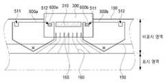
도 4a 및 도 4b는 본 발명의 일 실시예에 따른 디스플레이 장치에서 데이터 구동부를 데이터 패드에 얼라인하는 공정을 도시한 공정도로서, 이는 전술한 도 3에 따른 디스플레이 장치에 관한 것이다. 따라서, 동일한 구성에 대해서는 동일한 도면부호를 부여하였다. 구체적으로 도시하지는 않았지만, 게이트 구동부를 게이트 패드에 얼라인하는 공정도 후술하는 공정과 동일하다.4A and 4B are process diagrams illustrating a process of aligning a data driver with a data pad in a display device according to an exemplary embodiment of the present invention, which relates to the display device of FIG. 3 described above. Accordingly, the same reference numerals are assigned to the same configuration. Although not specifically shown, the process of aligning the gate driver with the gate pad is also the same as the process described later.
우선, 데이터 구동부(300)와 그에 대응하는 기판(100) 상의 구성들에 대해서 보다 구체적으로 설명한 후, 상기 얼라인 공정에 대해서 이어서 설명하기로 한다.First, the
도 4a에서 알 수 있듯이, 기판(100)의 표시 영역에서 비표시 영역으로 제2 전극(150)이 연장되어 있다. 또한, 상기 기판(100)의 비표시 영역에는 콘택 패드(500a, 500b)가 형성되어 있고, 상기 콘택 패드(500a, 500b)는 콘택홀(x)을 통해서 상기 제2 전극(150)과 전기적으로 연결되어 있다.As can be seen from FIG. 4A, the
상기 콘택 패드(500a, 500b)는 데이터 구동부(300)의 일측에 대응하는 제1 콘택 패드(500a) 및 데이터 구동부(300)의 타측에 대응하는 제2 콘택 패드(500b)를 포함하여 이루어진다.The
상기 제1 콘택 패드(500a)와 제2 콘택 패드(500b)는 하나의 데이터 구동부(300)와 연결되는 복수의 데이터 링크 배선(160)들, 즉, 하나의 데이터 링크 배선 세트를 중심으로 하여 좌우로 이격되어 있다. 복수의 데이터 링크 배선(160)들은 각각 데이터 패드(165)와 연결되어 있다.The
상기 제1 콘택 패드(500a) 및 제2 콘택 패드(500b) 각각은 그 일측부에 형성된 제1 수용홈(511) 및 그 타측부에 형성된 제2 수용홈(512)을 포함하여 이루어진다. 상기 제1 수용홈(511)과 상기 제2 수용홈(512)의 형상은 사각형 구조로 형성될 수 있지만 반드시 그에 한정되는 것은 아니다.Each of the first and
상기 데이터 구동부(300)는 데이터 구동 집적 회로(310)와 얼라인 마크(600a, 600b)를 구비하고 있다. 상기 얼라인 마크(600a, 600b)는 상기 데이터 구동부(300)의 일측부에 형성된 제1 얼라인 마크(600a) 및 상기 데이터 구동부(300)의 타측부에 형성된 제2 얼라인 마크(600b)를 포함하여 이루어진다.The
상기 제1 얼라인 마크(600a) 및 상기 제2 얼라인 마크(600b)의 형상은 사각형 구조로 형성될 수 있지만 반드시 그에 한정되는 것은 아니다.The shapes of the
상기 제1 얼라인 마크(600a)는 상기 제1 콘택 패드(500a)의 제2 수용홈(512) 내에 수용되고, 상기 제2 얼라인 마크(600b)는 상기 제2 콘택 패드(500b)의 제1 수용홈(511) 내에 수용된다. 이와 같이 하나의 데이터 구동부(300)에 제1 얼라인 마크(600a) 및 제2 얼라인 마크(600b)로 이루어진 2개의 얼라인 마크를 형성하고, 각각의 얼라인 마크를 서로 상이한 제1 콘택 패드(500a)의 수용홈 및 제2 콘택 패드(500b)의 수용홈 내에 수용되도록 함으로써 보다 정밀한 얼라인 공정을 수행할 수 있다.The
또한, 하나의 콘택 패드(500a, 500b)에 제1 수용홈(511) 및 제2 수용홈(512)을 형성하고, 상기 제1 수용홈(511) 및 제2 수용홈(512)에 서로 상이한 데이터 구동부(300)의 얼라인 마크(600)가 수용되도록 함으로써, 상기 콘택 패드(500a, 500b)의 개수를 증가시키지 않으면서도 정밀한 얼라인 공정을 수행할 수 있다.In addition, a
상기 제1 얼라인 마크(600a)의 폭(L1)은 상기 제1 콘택 패드(500a)의 제2 수용홈(512)의 폭(L2)보다 작게 형성된다. 또한, 상기 제2 얼라인 마크(600b)의 폭(L1)은 상기 제2 콘택 패드(500b)의 제1 수용홈(511)의 폭(L2)보다 작게 형성된다. 이는, 상기 제1 얼라인 마크(600a)의 폭(L1)이 상기 제1 콘택 패드(500a)의 제2 수용홈(512)의 폭(L2) 이상이거나 또는 상기 제2 얼라인 마크(600b)의 폭(L1)이 상기 제2 콘택 패드(500b)의 제1 수용홈(511)의 폭(L2) 이상이면 비젼(visiou)을 이용한 얼라인 공정을 수행할 수 없기 때문이다. 상기 폭(L1, L2)은 디스플레이 장치의 외곽 변에 평행한 방향의 폭을 의미한다. 예로서, 디스플레이 장치의 상측에서의 얼라인 공정을 수행할 경우에는 디스플레이 장치의 상부 변에 평행한 방향인 가로 방향의 폭을 의미하고, 디스플레이 장치의 좌측에서의 얼라인 공정을 수행할 경우에는 디스플레이 장치의 좌측 변에 평행한 방향인 세로 방향의 폭을 의미한다.The width L1 of the
이와 같은 구성의 데이터 구동부(300)를 데이터 패드(165)에 얼라인하는 공정을 설명하면 다음과 같다.A process of aligning the
우선, 도 4a에서 알 수 있듯이, 상기 데이터 구동부(300)에 형성된 제1 얼라인 마크(600a)가 상기 기판(100) 상에 형성된 제1 콘택 패드(500a)의 제2 수용홈(512) 내에 수용됨과 더불어 상기 데이터 구동부(300)에 형성된 제2 얼라인 마크(600b)가 상기 기판(100) 상에 형성된 제2 콘택 패드(500b)의 제1 수용홈(511) 내에 수용되도록, 상기 데이터 구동부(300)를 기판(100)의 상측으로 이동하면서 상기 데이터 구동부(300)의 위치를 조정한다.First, as can be seen in FIG. 4A, the
다음, 도 4b에서 알 수 있듯이, 상기 제1 얼라인 마크(600a)가 상기 제1 콘택 패드(500a)의 제2 수용홈(512) 내에 수용되고 상기 제2 얼라인 마크(600b)가 상기 제2 콘택 패드(500b)의 제1 수용홈(511) 내에 수용된 상태로 상기 데이터 구동부(300)를 하강하여 상기 데이터 구동부(300)와 상기 기판(10) 상에 형성된 데이터 패드(165)와의 얼라인 공정을 완료한다.Next, as can be seen from FIG. 4B, the
이상 설명한 본 발명의 일 실시예에 따르면, 표시 영역 내에서 광 방출을 위해 적용되는 전극, 예로서 유기 발광 표시장치의 음극과 전기적으로 연결되는 콘택 패드(500)에 수용홈을 형성하여 그 수용홈을 얼라인 마크로서 활용하기 때문에 기판(100) 상에 별도의 얼라인 마크를 형성할 필요가 없다.According to an embodiment of the present invention described above, a receiving groove is formed in an electrode applied for light emission within a display area, for example, a
또한, 본 발명의 일 실시예에 따르면, 게이트 구동부(200) 및 데이터 구동부(300)에 형성된 얼라인 마크(600)에 수용홈을 형성할 필요가 없기 때문에 얼라인 마크(600)의 크기를 줄일 수 있어 표시 면에서 인식되는 얼라인 마크(600)의 크기를 최소화할 수 있다. 따라서, 종래에 비하여 시인성이 향상되고 미감을 중요시하는 보더리스 디스플레이에도 적용이 가능하다.In addition, according to an embodiment of the present invention, the size of the
본 명세서에 신호 구동부는 상기 게이트 구동부(200)와 상기 데이터 구동부(300)를 통칭하는 것이고, 신호 패드는 상기 게이트 패드(175)와 상기 데이터 패드(165)를 통칭하는 것이다.In this specification, the signal driver is collectively referred to as the
이상은 디스플레이 장치로서 유기 발광 표시장치를 예로 들어 설명하였지만, 본 발명이 반드시 유기 발광 표시장치로 한정되는 것은 아니다. 예로서, 본 발명에 따른 디스플레이 장치가 액정 표시 장치로 이루어질 수도 있고, 이 경우, 상기 콘택 패드(500a, 500b)는 액정 표시 장치의 공통 전극과 전기적으로 연결될 수 있다.In the above description, an organic light emitting display device has been described as an example of the display device, but the present invention is not limited to the organic light emitting display device. For example, the display device according to the present invention may be formed of a liquid crystal display device, and in this case, the
이상 첨부된 도면을 참조하여 본 발명의 실시예들을 상세하게 설명하였으나, 본 발명은 반드시 이러한 실시예로 국한되는 것은 아니고, 본 발명의 기술사상을 벗어나지 않는 범위 내에서 다양하게 변형 실시될 수 있다. 따라서, 본 발명에 개시된 실시예들은 본 발명의 기술 사상을 한정하기 위한 것이 아니라 설명하기 위한 것이고, 이러한 실시예에 의하여 본 발명의 기술 사상의 범위가 한정되는 것은 아니다. 그러므로, 이상에서 기술한 실시예들은 모든 면에서 예시적인 것이며 한정적이 아닌 것으로 이해해야만 한다. 본 발명의 보호 범위는 청구 범위에 의하여 해석되어야 하며, 그와 동등한 범위 내에 있는 모든 기술 사상은 본 발명의 권리 범위에 포함되는 것으로 해석되어야 할 것이다Although the embodiments of the present invention have been described in detail with reference to the accompanying drawings, the present invention is not necessarily limited to these embodiments, and various modifications can be made without departing from the spirit of the present invention. Accordingly, the embodiments disclosed in the present invention are not intended to limit the technical idea of the present invention, but to explain the technical idea, and the scope of the technical idea of the present invention is not limited by these embodiments. Therefore, it should be understood that the embodiments described above are illustrative in all respects and not limiting. The scope of protection of the present invention should be interpreted by the claims, and all technical ideas within the scope equivalent thereto should be construed as being included in the scope of the present invention.
100: 기판 110: 게이트 배선
120: 데이터 배선 130: 고전위 전원 배선
140: 제1 전극 150: 제2 전극
160: 데이터 링크 배선 165: 데이터 패드
170: 게이트 링크 배선 175: 게이트 패드
200: 게이트 구동부 210: 게이트 구동 집적 회로
300: 데이터 구동부 310: 데이터 구동 집적 회로
500: 콘택 패드 500a, 500b: 제1, 제2 콘택 패드
600: 얼라인 마크 600a, 600b: 제1, 제2 얼라인 마크100: substrate 110: gate wiring
120: data wiring 130: high potential power wiring
140: first electrode 150: second electrode
160: data link wiring 165: data pad
170: gate link wiring 175: gate pad
200: gate driver 210: gate driving integrated circuit
300: data driver 310: data driving integrated circuit
500:
600:
Claims (6)
Translated fromKorean상기 기판의 표시 영역에 형성된 전극;
상기 기판의 비표시 영역에 형성되며, 상기 전극과 전기적으로 연결된 콘택 패드;
상기 기판의 비표시 영역에 형성된 신호 패드; 및
상기 기판의 비표시 영역에 형성되며, 상기 신호 패드와 연결된 신호 구동부를 포함하여 이루어지고,
상기 콘택 패드는 그 내부에 수용홈을 구비하고 있고, 상기 신호 구동부는 상기 수용홈에 수용되는 얼라인 마크를 구비하고 있는 디스플레이 장치.A substrate having a display area and a non-display area outside the display area;
An electrode formed in the display area of the substrate;
A contact pad formed in a non-display area of the substrate and electrically connected to the electrode;
A signal pad formed in a non-display area of the substrate; And
It is formed in the non-display area of the substrate and comprises a signal driver connected to the signal pad,
The contact pad has an accommodating groove therein, and the signal driver has an alignment mark accommodated in the accommodating groove.
상기 얼라인 마크의 폭은 상기 수용홈의 폭보다 작게 형성된 디스플레이 장치.The method of claim 1,
A display device having a width of the alignment mark smaller than a width of the receiving groove.
상기 콘택 패드는 상기 신호 구동부의 일측에 대응하는 제1 콘택 패드 및 상기 신호 구동부의 타측에 대응하는 제2 콘택 패드를 포함하고,
상기 얼라인 마크는 상기 신호 구동부의 일측에 형성된 제1 얼라인 마크 및 상기 신호 구동부의 타측에 형성된 제2 얼라인 마크를 포함하고,
상기 제1 얼라인 마크는 상기 제1 콘택 패드에 구비된 수용홈에 수용되고, 상기 제2 얼라인 마크는 상기 제2 콘택 패드에 구비된 수용홈에 수용되는 디스플레이 장치.The method of claim 1,
The contact pad includes a first contact pad corresponding to one side of the signal driver and a second contact pad corresponding to the other side of the signal driver,
The alignment mark includes a first alignment mark formed on one side of the signal driver and a second alignment mark formed on the other side of the signal driver,
The first alignment mark is accommodated in a receiving groove provided in the first contact pad, and the second alignment mark is received in a receiving groove provided in the second contact pad.
상기 콘택 패드에 구비된 수용홈은 상기 콘택 패드의 일측에 형성된 제1 수용홈 및 상기 콘택 패드의 타측에 형성된 제2 수용홈을 포함하고,
상기 제1 수용홈 내에 수용되는 얼라인 마크와 상기 제2 수용홈 내에 수용되는 얼라인 마크는 서로 상이한 신호 구동부에 형성된 디스플레이 장치.The method of claim 1,
The receiving groove provided in the contact pad includes a first receiving groove formed on one side of the contact pad and a second receiving groove formed on the other side of the contact pad,
An alignment mark accommodated in the first accommodating groove and an alignment mark accommodated in the second accommodating groove are formed in different signal driving units.
상기 전극은 상기 기판의 비표시 영역으로 연장되어 있고, 상기 전극은 상기 비표시 영역에 형성된 콘택홀을 통해서 상기 콘택 패드와 전기적으로 연결된 디스플레이 장치.The method of claim 1,
The electrode is extended to a non-display area of the substrate, and the electrode is electrically connected to the contact pad through a contact hole formed in the non-display area.
상기 기판의 표시 영역에는 발광 다이오드가 추가로 형성되어 있고, 상기 전극은 상기 발광 다이오드와 연결된 디스플레이 장치.The method of claim 1,
A light emitting diode is additionally formed in the display area of the substrate, and the electrode is connected to the light emitting diode.
Priority Applications (4)
| Application Number | Priority Date | Filing Date | Title |
|---|---|---|---|
| KR1020140091725AKR102163358B1 (en) | 2014-07-21 | 2014-07-21 | Display Device |
| EP14196085.6AEP2978286B1 (en) | 2014-07-21 | 2014-12-03 | Display device |
| US14/561,932US9082774B1 (en) | 2014-07-21 | 2014-12-05 | Display device |
| CN201410818151.8ACN105321457B (en) | 2014-07-21 | 2014-12-24 | Display device and the method for forming display device |
Applications Claiming Priority (1)
| Application Number | Priority Date | Filing Date | Title |
|---|---|---|---|
| KR1020140091725AKR102163358B1 (en) | 2014-07-21 | 2014-07-21 | Display Device |
Publications (2)
| Publication Number | Publication Date |
|---|---|
| KR20160011259A KR20160011259A (en) | 2016-02-01 |
| KR102163358B1true KR102163358B1 (en) | 2020-10-12 |
Family
ID=52015902
Family Applications (1)
| Application Number | Title | Priority Date | Filing Date |
|---|---|---|---|
| KR1020140091725AActiveKR102163358B1 (en) | 2014-07-21 | 2014-07-21 | Display Device |
Country Status (4)
| Country | Link |
|---|---|
| US (1) | US9082774B1 (en) |
| EP (1) | EP2978286B1 (en) |
| KR (1) | KR102163358B1 (en) |
| CN (1) | CN105321457B (en) |
Families Citing this family (12)
| Publication number | Priority date | Publication date | Assignee | Title |
|---|---|---|---|---|
| US10665578B2 (en) | 2015-09-24 | 2020-05-26 | Apple Inc. | Display with embedded pixel driver chips |
| KR102465968B1 (en)* | 2015-11-24 | 2022-11-10 | 삼성전자주식회사 | Semiconductor chip, method of fabricating the semiconductor chip, and semiconductor package and display apparatus comprising the semiconductor chip |
| KR20170113748A (en)* | 2016-03-24 | 2017-10-13 | 삼성디스플레이 주식회사 | Display apparatus and method of manufacturing the same |
| KR102637015B1 (en)* | 2016-06-08 | 2024-02-16 | 삼성디스플레이 주식회사 | Display apparatus and manufacturing method thereof |
| KR102636736B1 (en)* | 2016-09-08 | 2024-02-15 | 삼성디스플레이 주식회사 | Display device |
| CN106973485A (en)* | 2017-03-14 | 2017-07-21 | 惠科股份有限公司 | Display device and flexible circuit board thereof |
| KR102316563B1 (en)* | 2017-05-22 | 2021-10-25 | 엘지디스플레이 주식회사 | Organic Light-Emitting Display device having an upper substrate formed by a metal and Method of fabricating the same |
| CN107770957B (en)* | 2017-09-26 | 2019-06-14 | 武汉天马微电子有限公司 | Flexible line way board module and display device |
| KR102395221B1 (en)* | 2017-12-05 | 2022-05-10 | 삼성디스플레이 주식회사 | Display device |
| CN117525060A (en)* | 2018-02-28 | 2024-02-06 | 苹果公司 | Display with embedded pixel driver chip |
| KR20210150649A (en)* | 2020-06-03 | 2021-12-13 | 삼성디스플레이 주식회사 | Display device |
| CN113805378B (en) | 2020-06-12 | 2022-07-26 | 京东方科技集团股份有限公司 | Light-emitting substrate and display device |
Citations (2)
| Publication number | Priority date | Publication date | Assignee | Title |
|---|---|---|---|---|
| US20070040286A1 (en) | 2005-08-17 | 2007-02-22 | Au Optronics Corp. | Structure for circuit assembly |
| WO2013030888A1 (en) | 2011-08-31 | 2013-03-07 | パナソニック株式会社 | Display-panel device and manufacturing method therefor |
Family Cites Families (15)
| Publication number | Priority date | Publication date | Assignee | Title |
|---|---|---|---|---|
| JP3429775B2 (en)* | 1995-08-07 | 2003-07-22 | 株式会社 日立製作所 | Active matrix type liquid crystal display device suitable for countermeasures against static electricity |
| KR100652053B1 (en)* | 2003-06-28 | 2006-11-30 | 엘지.필립스 엘시디 주식회사 | Method for fabricating of liquid crystal display device |
| KR100930917B1 (en)* | 2003-06-30 | 2009-12-10 | 엘지디스플레이 주식회사 | Liquid crystal panel arrangement and liquid crystal panel exposure method |
| KR101223098B1 (en)* | 2004-09-09 | 2013-01-17 | 삼성디스플레이 주식회사 | Display device and method of manufacturing the same |
| KR101127855B1 (en)* | 2005-06-02 | 2012-03-21 | 엘지디스플레이 주식회사 | LCD display device |
| KR101183374B1 (en)* | 2005-06-27 | 2012-09-21 | 엘지디스플레이 주식회사 | Liquid crystal display device and method of lcd thereof |
| KR101140241B1 (en)* | 2005-06-27 | 2012-04-26 | 엘지디스플레이 주식회사 | Liquid crsytal display device using allign mark |
| CN1924985A (en)* | 2005-08-31 | 2007-03-07 | 中华映管股份有限公司 | Correction method for joint offset between flat panel display and display panel and driving chip |
| CN100461984C (en)* | 2005-09-30 | 2009-02-11 | 友达光电股份有限公司 | Circuit Assembly Structure |
| KR20070106261A (en)* | 2006-04-28 | 2007-11-01 | 엘지.필립스 엘시디 주식회사 | LCD Display |
| KR20070117110A (en)* | 2006-06-07 | 2007-12-12 | 엘지.필립스 엘시디 주식회사 | Tape carrier package and liquid crystal display including the same |
| JP5425363B2 (en)* | 2006-11-28 | 2014-02-26 | ルネサスエレクトロニクス株式会社 | Semiconductor device and display device |
| TWI424411B (en)* | 2009-12-31 | 2014-01-21 | Au Optronics Corp | Electroluminescence device |
| KR101484642B1 (en)* | 2012-10-24 | 2015-01-20 | 엘지디스플레이 주식회사 | Organic light emitting display device |
| CN103268035A (en)* | 2013-06-07 | 2013-08-28 | 友达光电股份有限公司 | A pairing method of a thin film transistor liquid crystal display device |
- 2014
- 2014-07-21KRKR1020140091725Apatent/KR102163358B1/enactiveActive
- 2014-12-03EPEP14196085.6Apatent/EP2978286B1/enactiveActive
- 2014-12-05USUS14/561,932patent/US9082774B1/enactiveActive
- 2014-12-24CNCN201410818151.8Apatent/CN105321457B/enactiveActive
Patent Citations (2)
| Publication number | Priority date | Publication date | Assignee | Title |
|---|---|---|---|---|
| US20070040286A1 (en) | 2005-08-17 | 2007-02-22 | Au Optronics Corp. | Structure for circuit assembly |
| WO2013030888A1 (en) | 2011-08-31 | 2013-03-07 | パナソニック株式会社 | Display-panel device and manufacturing method therefor |
Also Published As
| Publication number | Publication date |
|---|---|
| CN105321457A (en) | 2016-02-10 |
| EP2978286A1 (en) | 2016-01-27 |
| KR20160011259A (en) | 2016-02-01 |
| EP2978286B1 (en) | 2020-03-18 |
| US9082774B1 (en) | 2015-07-14 |
| CN105321457B (en) | 2018-12-04 |
Similar Documents
| Publication | Publication Date | Title |
|---|---|---|
| KR102163358B1 (en) | Display Device | |
| KR102151099B1 (en) | Display panel and large format display apparatus using the same | |
| KR102183494B1 (en) | Organic Light Emitting Display Device | |
| EP2950349B1 (en) | Organic light emitting display device and method of manufacturing the same | |
| KR101484642B1 (en) | Organic light emitting display device | |
| KR102245304B1 (en) | Display device with power supply in cover type | |
| KR102426617B1 (en) | Display device and manufacturing method for the same | |
| KR102493858B1 (en) | Electroluminescent Display Device | |
| KR102362093B1 (en) | Display device | |
| US10211275B2 (en) | Organic light emitting diode display panel with pads and organic light emitting diode display device having the same | |
| KR102544942B1 (en) | Display Device And Method Of Fabricating The Same | |
| KR20210085642A (en) | Display device | |
| KR102532973B1 (en) | Display device and its fabricating method | |
| KR102099901B1 (en) | Organic light emitting display device | |
| KR101974251B1 (en) | Display module | |
| KR102343653B1 (en) | Display device and manufacturing method of the same | |
| KR102521759B1 (en) | Liquid crystal display device | |
| KR102123444B1 (en) | Organic light emitting display evice | |
| KR20170077917A (en) | Flat Panel Display Having A Dummy Pixel For Preventing Electrottatic Damage | |
| KR20170071974A (en) | Flexible display device | |
| KR20200080899A (en) | Display device | |
| KR102141409B1 (en) | Organic Light Emitting Display Device | |
| KR102242350B1 (en) | Organic Light Emitting Display Device | |
| KR102174998B1 (en) | Organic Light Emitting Display Device | |
| KR102450960B1 (en) | Display device |
Legal Events
| Date | Code | Title | Description |
|---|---|---|---|
| PA0109 | Patent application | St.27 status event code:A-0-1-A10-A12-nap-PA0109 | |
| PG1501 | Laying open of application | St.27 status event code:A-1-1-Q10-Q12-nap-PG1501 | |
| A201 | Request for examination | ||
| PA0201 | Request for examination | St.27 status event code:A-1-2-D10-D11-exm-PA0201 | |
| E701 | Decision to grant or registration of patent right | ||
| PE0701 | Decision of registration | St.27 status event code:A-1-2-D10-D22-exm-PE0701 | |
| PR0701 | Registration of establishment | St.27 status event code:A-2-4-F10-F11-exm-PR0701 | |
| PR1002 | Payment of registration fee | St.27 status event code:A-2-2-U10-U11-oth-PR1002 Fee payment year number:1 | |
| PG1601 | Publication of registration | St.27 status event code:A-4-4-Q10-Q13-nap-PG1601 | |
| PR1001 | Payment of annual fee | St.27 status event code:A-4-4-U10-U11-oth-PR1001 Fee payment year number:4 | |
| PR1001 | Payment of annual fee | St.27 status event code:A-4-4-U10-U11-oth-PR1001 Fee payment year number:5 | |
| PR1001 | Payment of annual fee | St.27 status event code:A-4-4-U10-U11-oth-PR1001 Fee payment year number:6 |