KR102162797B1 - Method for manufacturing of organic light emitting display apparatus - Google Patents
Method for manufacturing of organic light emitting display apparatusDownload PDFInfo
- Publication number
- KR102162797B1 KR102162797B1KR1020130161780AKR20130161780AKR102162797B1KR 102162797 B1KR102162797 B1KR 102162797B1KR 1020130161780 AKR1020130161780 AKR 1020130161780AKR 20130161780 AKR20130161780 AKR 20130161780AKR 102162797 B1KR102162797 B1KR 102162797B1
- Authority
- KR
- South Korea
- Prior art keywords
- substrate
- deposition
- layer
- assembly
- mask assembly
- Prior art date
- Legal status (The legal status is an assumption and is not a legal conclusion. Google has not performed a legal analysis and makes no representation as to the accuracy of the status listed.)
- Active
Links
- 238000004519manufacturing processMethods0.000titleclaimsabstractdescription29
- 238000000034methodMethods0.000titleclaimsdescription37
- 239000010410layerSubstances0.000claimsabstractdescription416
- 238000000151depositionMethods0.000claimsabstractdescription401
- 230000008021depositionEffects0.000claimsabstractdescription375
- 239000000758substrateSubstances0.000claimsabstractdescription213
- 239000000463materialSubstances0.000claimsabstractdescription66
- 239000012044organic layerSubstances0.000claimsabstractdescription7
- 238000000429assemblyMethods0.000claimsdescription23
- 230000000712assemblyEffects0.000claimsdescription23
- 230000000903blocking effectEffects0.000claimsdescription17
- 238000000059patterningMethods0.000claimsdescription11
- 239000003086colorantSubstances0.000claimsdescription6
- 238000007740vapor depositionMethods0.000claimsdescription2
- 238000010030laminatingMethods0.000claims1
- 238000002347injectionMethods0.000description22
- 239000007924injectionSubstances0.000description22
- 230000005525hole transportEffects0.000description20
- 230000008020evaporationEffects0.000description16
- 238000001704evaporationMethods0.000description16
- 239000004065semiconductorSubstances0.000description9
- 239000011521glassSubstances0.000description3
- 230000008569processEffects0.000description3
- 239000010409thin filmSubstances0.000description3
- 229910001111Fine metalInorganic materials0.000description2
- 230000008901benefitEffects0.000description2
- 230000015572biosynthetic processEffects0.000description2
- 238000009795derivationMethods0.000description2
- 230000000694effectsEffects0.000description2
- 239000010408filmSubstances0.000description2
- 230000014509gene expressionEffects0.000description2
- 239000011229interlayerSubstances0.000description2
- 239000011159matrix materialSubstances0.000description2
- 239000011241protective layerSubstances0.000description2
- 229910021417amorphous siliconInorganic materials0.000description1
- 239000000470constituentSubstances0.000description1
- 229910021419crystalline siliconInorganic materials0.000description1
- 238000005137deposition processMethods0.000description1
- 238000005516engineering processMethods0.000description1
- 238000010438heat treatmentMethods0.000description1
- 238000005339levitationMethods0.000description1
- 239000007769metal materialSubstances0.000description1
- 238000012986modificationMethods0.000description1
- 230000004048modificationEffects0.000description1
- 230000004044responseEffects0.000description1
- 230000009466transformationEffects0.000description1
- 238000000844transformationMethods0.000description1
- 239000012780transparent materialSubstances0.000description1
Images


Classifications
- H—ELECTRICITY
- H05—ELECTRIC TECHNIQUES NOT OTHERWISE PROVIDED FOR
- H05B—ELECTRIC HEATING; ELECTRIC LIGHT SOURCES NOT OTHERWISE PROVIDED FOR; CIRCUIT ARRANGEMENTS FOR ELECTRIC LIGHT SOURCES, IN GENERAL
- H05B33/00—Electroluminescent light sources
- H05B33/10—Apparatus or processes specially adapted to the manufacture of electroluminescent light sources
- C—CHEMISTRY; METALLURGY
- C23—COATING METALLIC MATERIAL; COATING MATERIAL WITH METALLIC MATERIAL; CHEMICAL SURFACE TREATMENT; DIFFUSION TREATMENT OF METALLIC MATERIAL; COATING BY VACUUM EVAPORATION, BY SPUTTERING, BY ION IMPLANTATION OR BY CHEMICAL VAPOUR DEPOSITION, IN GENERAL; INHIBITING CORROSION OF METALLIC MATERIAL OR INCRUSTATION IN GENERAL
- C23C—COATING METALLIC MATERIAL; COATING MATERIAL WITH METALLIC MATERIAL; SURFACE TREATMENT OF METALLIC MATERIAL BY DIFFUSION INTO THE SURFACE, BY CHEMICAL CONVERSION OR SUBSTITUTION; COATING BY VACUUM EVAPORATION, BY SPUTTERING, BY ION IMPLANTATION OR BY CHEMICAL VAPOUR DEPOSITION, IN GENERAL
- C23C14/00—Coating by vacuum evaporation, by sputtering or by ion implantation of the coating forming material
- C23C14/04—Coating on selected surface areas, e.g. using masks
- C23C14/042—Coating on selected surface areas, e.g. using masks using masks
- C—CHEMISTRY; METALLURGY
- C23—COATING METALLIC MATERIAL; COATING MATERIAL WITH METALLIC MATERIAL; CHEMICAL SURFACE TREATMENT; DIFFUSION TREATMENT OF METALLIC MATERIAL; COATING BY VACUUM EVAPORATION, BY SPUTTERING, BY ION IMPLANTATION OR BY CHEMICAL VAPOUR DEPOSITION, IN GENERAL; INHIBITING CORROSION OF METALLIC MATERIAL OR INCRUSTATION IN GENERAL
- C23C—COATING METALLIC MATERIAL; COATING MATERIAL WITH METALLIC MATERIAL; SURFACE TREATMENT OF METALLIC MATERIAL BY DIFFUSION INTO THE SURFACE, BY CHEMICAL CONVERSION OR SUBSTITUTION; COATING BY VACUUM EVAPORATION, BY SPUTTERING, BY ION IMPLANTATION OR BY CHEMICAL VAPOUR DEPOSITION, IN GENERAL
- C23C14/00—Coating by vacuum evaporation, by sputtering or by ion implantation of the coating forming material
- C23C14/22—Coating by vacuum evaporation, by sputtering or by ion implantation of the coating forming material characterised by the process of coating
- C23C14/56—Apparatus specially adapted for continuous coating; Arrangements for maintaining the vacuum, e.g. vacuum locks
- H—ELECTRICITY
- H10—SEMICONDUCTOR DEVICES; ELECTRIC SOLID-STATE DEVICES NOT OTHERWISE PROVIDED FOR
- H10K—ORGANIC ELECTRIC SOLID-STATE DEVICES
- H10K59/00—Integrated devices, or assemblies of multiple devices, comprising at least one organic light-emitting element covered by group H10K50/00
- H10K59/10—OLED displays
- H10K59/12—Active-matrix OLED [AMOLED] displays
- H10K59/121—Active-matrix OLED [AMOLED] displays characterised by the geometry or disposition of pixel elements
- H—ELECTRICITY
- H10—SEMICONDUCTOR DEVICES; ELECTRIC SOLID-STATE DEVICES NOT OTHERWISE PROVIDED FOR
- H10K—ORGANIC ELECTRIC SOLID-STATE DEVICES
- H10K59/00—Integrated devices, or assemblies of multiple devices, comprising at least one organic light-emitting element covered by group H10K50/00
- H10K59/30—Devices specially adapted for multicolour light emission
- H10K59/35—Devices specially adapted for multicolour light emission comprising red-green-blue [RGB] subpixels
- H—ELECTRICITY
- H10—SEMICONDUCTOR DEVICES; ELECTRIC SOLID-STATE DEVICES NOT OTHERWISE PROVIDED FOR
- H10K—ORGANIC ELECTRIC SOLID-STATE DEVICES
- H10K71/00—Manufacture or treatment specially adapted for the organic devices covered by this subclass
- H10K71/10—Deposition of organic active material
- H10K71/16—Deposition of organic active material using physical vapour deposition [PVD], e.g. vacuum deposition or sputtering
- H10K71/166—Deposition of organic active material using physical vapour deposition [PVD], e.g. vacuum deposition or sputtering using selective deposition, e.g. using a mask
- H—ELECTRICITY
- H10—SEMICONDUCTOR DEVICES; ELECTRIC SOLID-STATE DEVICES NOT OTHERWISE PROVIDED FOR
- H10K—ORGANIC ELECTRIC SOLID-STATE DEVICES
- H10K71/00—Manufacture or treatment specially adapted for the organic devices covered by this subclass
- H—ELECTRICITY
- H10—SEMICONDUCTOR DEVICES; ELECTRIC SOLID-STATE DEVICES NOT OTHERWISE PROVIDED FOR
- H10K—ORGANIC ELECTRIC SOLID-STATE DEVICES
- H10K71/00—Manufacture or treatment specially adapted for the organic devices covered by this subclass
- H10K71/20—Changing the shape of the active layer in the devices, e.g. patterning
Landscapes
- Chemical & Material Sciences (AREA)
- Engineering & Computer Science (AREA)
- Chemical Kinetics & Catalysis (AREA)
- Materials Engineering (AREA)
- Mechanical Engineering (AREA)
- Metallurgy (AREA)
- Organic Chemistry (AREA)
- Manufacturing & Machinery (AREA)
- Physics & Mathematics (AREA)
- Geometry (AREA)
- Microelectronics & Electronic Packaging (AREA)
- Electroluminescent Light Sources (AREA)
Abstract
Translated fromKorean
Description
Translated fromKorean본 발명의 실시예들은 유기 발광 디스플레이 장치의 제조 방법에 관한 것이다.Embodiments of the present invention relate to a method of manufacturing an organic light emitting display device.
디스플레이 장치들 중, 유기 발광 디스플레이 장치는 시야각이 넓고 컨트라스트가 우수할 뿐만 아니라 응답속도가 빠르다는 장점을 가지고 있어 차세대 디스플레이 장치로서 주목을 받고 있다.Among the display devices, the organic light emitting display device is attracting attention as a next-generation display device because it has the advantage of having a wide viewing angle, excellent contrast, and fast response speed.
유기 발광 디스플레이 장치는 서로 대향된 제1 전극 및 제2 전극 사이에 발광층 및 이를 포함하는 중간층을 구비한다. 이때 상기 전극들 및 중간층은 여러 방법으로 형성될 수 있는데, 그 중 한 방법이 독립 증착 방식이다. 증착 방법을 이용하여 유기 발광 디스플레이 장치를 제작하기 위해서는, 유기층 등이 형성될 기판 면에, 형성될 유기층 등의 패턴과 동일한 패턴을 가지는 파인 메탈 마스크(fine metal mask: FMM)를 밀착시키고 유기층 등의 재료를 증착하여 소정 패턴의 유기층을 형성한다.An organic light emitting display device includes a light emitting layer and an intermediate layer including the same between a first electrode and a second electrode opposite to each other. At this time, the electrodes and the intermediate layer may be formed by several methods, one of which is an independent deposition method. In order to fabricate an organic light emitting display device using a vapor deposition method, a fine metal mask (FMM) having the same pattern as the pattern of the organic layer to be formed is adhered to the surface of the substrate on which the organic layer is to be formed, etc. The material is deposited to form an organic layer of a predetermined pattern.
전술한 배경기술은 발명자가 본 발명의 도출을 위해 보유하고 있었거나, 본 발명의 도출 과정에서 습득한 기술 정보로서, 반드시 본 발명의 출원 전에 일반 공중에게 공개된 공지기술이라 할 수는 없다.The above-described background technology is technical information possessed by the inventors for derivation of the present invention or acquired during the derivation process of the present invention, and is not necessarily known to be publicly known prior to filing the present invention.
본 발명의 실시예들은 유기 발광 디스플레이 장치의 제조 방법을 제공한다.Embodiments of the present invention provide a method of manufacturing an organic light emitting display device.
본 발명의 일 실시예는 기판상에 유기층을 형성하는 증착 장치를 이용한 유기 발광 디스플레이 장치의 제조 방법에 있어서, 로딩부에서 상기 기판을 공통층 증착용 마스크 어셈블리 또는 패턴층 증착용 마스크 어셈블리에 고정시키는 단계; 증착부 내에 배치된 하나 이상의 증착 어셈블리와 상기 공통층 증착용 마스크 어셈블리 또는 패턴층 증착용 마스크 어셈블리에 고정된 상기 기판이 소정 정도 이격된 상태에서, 제1 이송부에 의해 상기 기판이 상기 증착 어셈블리에 대해 상대적으로 이동하면서 상기 증착 어셈블리로부터 발산된 증착 물질이 상기 기판에 증착되어 중간층이 형성되는 단계; 및 언로딩부에서 증착이 완료된 상기 기판을 상기 공통층 증착용 마스크 어셈블리 또는 패턴층 증착용 마스크 어셈블리로부터 분리시키는 단계;를 포함하는 유기 발광 디스플레이 장치의 제조 방법을 개시한다.According to an embodiment of the present invention, in a method of manufacturing an organic light emitting display device using a deposition apparatus for forming an organic layer on a substrate, the substrate is fixed to a mask assembly for depositing a common layer or a mask assembly for depositing a pattern layer in a loading unit. step; In a state where at least one deposition assembly disposed in the deposition unit and the substrate fixed to the common layer deposition mask assembly or the pattern layer deposition mask assembly are spaced apart by a predetermined degree, the substrate is moved to the deposition assembly by a first transfer unit. Depositing a deposition material emanating from the deposition assembly while moving relatively to the substrate to form an intermediate layer; And separating the substrate, which has been deposited by an unloading unit, from the common layer deposition mask assembly or the pattern layer deposition mask assembly.
본 실시예에 있어서, 상기 로딩부에서 상기 기판이 상기 공통층 증착용 마스크 어셈블리에 고정되고, 상기 기판상에는 상기 증착 물질이 공통층으로 형성될 수 있다.In this embodiment, the substrate may be fixed to the common layer deposition mask assembly in the loading part, and the deposition material may be formed as a common layer on the substrate.
본 실시예에 있어서, 상기 중간층이 형성되는 단계는, 상기 기판상에 적어도 적색 발광층, 녹색 발광층, 청색 발광층이 공통층으로 적층될 수 있다.In the present embodiment, in the step of forming the intermediate layer, at least a red emission layer, a green emission layer, and a blue emission layer may be stacked as a common layer on the substrate.
본 실시예에 있어서, 상기 로딩부에서 상기 기판이 상기 패턴층 증착용 마스크 어셈블리에 고정되고, 상기 기판상에는 상기 증착 물질이 소정의 형상으로 패터닝되어 형성될 수 있다.In this embodiment, the substrate may be fixed to the pattern layer deposition mask assembly in the loading part, and the deposition material may be patterned into a predetermined shape on the substrate.
본 실시예에 있어서, 상기 중간층이 형성되는 단계는, 상기 기판상에 적색 발광층, 녹색 발광층, 청색 발광층이 각각 패턴층으로 형성될 수 있다.In this embodiment, in the step of forming the intermediate layer, a red emission layer, a green emission layer, and a blue emission layer may be formed as pattern layers on the substrate.
본 실시예에 있어서, 상기 공통층 증착용 마스크 어셈블리 또는 패턴층 증착용 마스크 어셈블리가 선택적으로 상기 기판과 결합할 수 있다.In this embodiment, the common layer deposition mask assembly or the pattern layer deposition mask assembly may be selectively combined with the substrate.
본 실시예에 있어서, 상기 로딩부에서 상기 기판이 상기 패턴층 증착용 마스크 어셈블리에 고정되고, 상기 중간층이 형성되는 단계는, 상기 기판이 상기 증착 어셈블리에 대해 상대적으로 이동하면서 상기 기판상에 어느 하나의 발광층이 증착되는 단계; 상기 기판이 고정된 상기 패턴층 증착용 마스크 어셈블리가 회송되는 단계; 상기 기판이 상기 증착 어셈블리에 대해 상대적으로 이동하면서 상기 기판상에 다른 하나의 발광층이 증착되는 단계;를 포함할 수 있다.In the present embodiment, the step of fixing the substrate to the pattern layer deposition mask assembly in the loading unit and forming the intermediate layer may include any one on the substrate while the substrate moves relative to the deposition assembly. Depositing a light emitting layer of; Returning the pattern layer deposition mask assembly to which the substrate is fixed; And depositing another emission layer on the substrate while the substrate moves relative to the deposition assembly.
본 실시예에 있어서, 하나의 발광층이 증착되는 동안, 다른 발광층용 증착 물질을 구비하는 증착 어셈블리와 기판 사이에는 차단 부재가 형성될 수 있다.In this embodiment, while one light emitting layer is being deposited, a blocking member may be formed between the substrate and the deposition assembly including the deposition material for the other light emitting layer.
본 실시예에 있어서, 상기 기판이 고정된 상기 패턴층 증착용 마스크 어셈블리가 회송된 후, 상기 패턴층 증착용 마스크 어셈블리가 상기 기판에 대해 일정 정도 오프셋되는 단계를 더 포함할 수 있다.In this embodiment, after the pattern layer deposition mask assembly to which the substrate is fixed is returned, the step of offsetting the pattern layer deposition mask assembly with respect to the substrate by a certain degree may be further included.
본 실시예에 있어서, 상기 중간층이 형성되는 단계는, 상기 기판이 상기 공통층 증착용 마스크 어셈블리에 고정된 상태에서 상기 기판이 상기 증착 어셈블리에 대해 상대적으로 이동하면서 상기 기판상에 하나 이상의 공통층이 증착되는 단계; 상기 기판이 상기 공통층 증착용 마스크 어셈블리로부터 분리되고, 상기 패턴층 증착용 마스크 어셈블리에 고정되는 단계; 상기 기판이 상기 패턴층 증착용 마스크 어셈블리에 고정된 상태에서 상기 기판이 상기 증착 어셈블리에 대해 상대적으로 이동하면서 상기 기판상에 적색 발광층, 녹색 발광층, 청색 발광층이 각각 패터닝 되는 단계;를 포함할 수 있다.In the present embodiment, the step of forming the intermediate layer includes at least one common layer on the substrate while the substrate is moved relative to the deposition assembly while the substrate is fixed to the common layer deposition mask assembly. Being deposited; Separating the substrate from the common layer deposition mask assembly and fixing it to the pattern layer deposition mask assembly; And patterning a red emission layer, a green emission layer, and a blue emission layer on the substrate while the substrate is relatively moved with respect to the deposition assembly while the substrate is fixed to the pattern layer deposition mask assembly. .
본 실시예에 있어서, 상기 기판상에 발광층이 패터닝 되는 단계는, 상기 기판상에 하나의 발광층이 패터닝된 후, 상기 패턴층 증착용 마스크 어셈블리가 상기 기판에 대해 일정 정도 오프셋되는 단계를 포함할 수 있다.In this embodiment, the step of patterning the light emitting layer on the substrate may include a step of offsetting the pattern layer deposition mask assembly with respect to the substrate by a certain degree after one light emitting layer is patterned on the substrate. have.
본 실시예에 있어서, 상기 기판상에 발광층이 패터닝 되는 단계 이후, 상기 기판이 상기 패턴층 증착용 마스크 어셈블리로부터 분리되고, 상기 공통층 증착용 마스크 어셈블리에 고정되는 단계; 상기 기판이 상기 공통층 증착용 마스크 어셈블리에 고정된 상태에서 상기 기판이 상기 증착 어셈블리에 대해 상대적으로 이동하면서 상기 기판상에 하나 이상의 공통층이 증착되는 단계;를 더 포함할 수 있다.In this embodiment, after the step of patterning the light emitting layer on the substrate, the substrate is separated from the pattern layer deposition mask assembly and fixed to the common layer deposition mask assembly; The method may further include depositing at least one common layer on the substrate while the substrate is moved relative to the deposition assembly while the substrate is fixed to the common layer deposition mask assembly.
본 실시예에 있어서, 상기 중간층이 형성되는 단계는, 상기 기판상의 어느 한가지 색을 방출하는 부화소 영역에 적어도 발광층을 포함하는 하나 이상의 중간층이 차례로 적층되어 형성되는 단계; 상기 기판상의 다른 색을 방출하는 부화소 영역에 적어도 발광층을 포함하는 하나 이상의 중간층이 차례로 적층되어 형성되는 단계; 및 상기 기판상의 또 다른 색을 방출하는 부화소 영역에 적어도 발광층을 포함하는 하나 이상의 중간층이 차례로 적층되어 형성되는 단계;를 포함할 수 있다.In this embodiment, the step of forming the intermediate layer may include forming one or more intermediate layers including at least a light emitting layer sequentially stacked in a subpixel region emitting one color on the substrate; Forming one or more intermediate layers including at least an emission layer sequentially stacked in a subpixel area emitting different colors on the substrate; And one or more intermediate layers including at least a light emitting layer are sequentially stacked and formed in a subpixel region emitting another color on the substrate.
본 실시예에 있어서, 상기 단계들 이후에, 상기 기판상의 또 다른 부화소 영역에, 적색 발광층, 녹색 발광층, 청색 발광층이 적층 형성되는 단계를 더 포함할 수 있다.In the present exemplary embodiment, after the above steps, a step of forming a red emission layer, a green emission layer, and a blue emission layer in another subpixel area on the substrate may be further included.
본 실시예에 있어서, 상기 중간층이 형성되는 단계는, 상기 기판상에 하나 이상의 공통층이 형성되는 단계; 상기 기판상에 각각의 부화소 영역에 각각의 발광층들이 차례로 패터닝되는 단계; 및 상기 기판상에 하나 이상의 공통층이 형성되는 단계;를 포함할 수 있다.In this embodiment, the step of forming the intermediate layer may include forming one or more common layers on the substrate; Sequentially patterning each of the light emitting layers in each subpixel area on the substrate; And forming one or more common layers on the substrate.
본 실시예에 있어서, 상기 공통층 증착용 마스크 어셈블리 또는 패턴층 증착용 마스크 어셈블리가 제2 이송부를 이용하여 회송되는 단계를 더 포함할 수 있다.In the present embodiment, the step of returning the common layer deposition mask assembly or the pattern layer deposition mask assembly using a second transfer unit may be further included.
본 실시예에 있어서, 상기 공통층 증착용 마스크 어셈블리 또는 패턴층 증착용 마스크 어셈블리는 상기 제1 이송부와 상기 제2 이송부 사이를 순환할 수 있다.In this embodiment, the common layer deposition mask assembly or the pattern layer deposition mask assembly may circulate between the first transfer unit and the second transfer unit.
본 실시예에 있어서, 상기 공통층 증착용 마스크 어셈블리 또는 패턴층 증착용 마스크 어셈블리는 각각, 하나 이상의 개구부가 형성되어 기판의 증착 영역을 정의하는 마스크; 일면 상에 상기 마스크가 안착되는 마스크 트레이; 및 상기 기판에서 상기 마스크와 접촉하는 면의 반대측 면에 형성되어 상기 마스크에 소정의 자기력을 가하는 마그넷 플레이트;를 포함할 수 있다.In this embodiment, the common layer deposition mask assembly or the pattern layer deposition mask assembly may include a mask having one or more openings to define a deposition area of the substrate; A mask tray on which the mask is mounted on one side; And a magnet plate formed on a surface opposite to a surface of the substrate in contact with the mask to apply a predetermined magnetic force to the mask.
본 실시예에 있어서, 상기 마그넷 플레이트는 상기 마스크를 상기 마그넷 플레이트 쪽으로 당기는 방향으로 자기력을 발생시킬 수 있다.In this embodiment, the magnet plate may generate a magnetic force in a direction pulling the mask toward the magnet plate.
본 실시예에 있어서, 상기 증착부 내부에 복수의 증착 어셈블리들이 구비되어 각 증착 어셈블리들에 의해 상기 기판에 연속적으로 증착이 이루어질 수 있다.In this embodiment, a plurality of deposition assemblies may be provided inside the deposition unit so that deposition may be continuously performed on the substrate by each deposition assembly.
전술한 것 외의 다른 측면, 특징, 이점이 이하의 도면, 특허청구범위 및 발명의 상세한 설명으로부터 명확해질 것이다.Other aspects, features, and advantages other than those described above will become apparent from the following drawings, claims, and detailed description of the invention.
본 발명의 실시예들에 관한 유기 발광 디스플레이 장치의 제조 방법은 공간효율성 및 제조효율성이 향상된다.In the manufacturing method of the organic light emitting display device according to the exemplary embodiments of the present invention, space efficiency and manufacturing efficiency are improved.
도 1은 본 발명의 일 실시예에 관한 증착 장치를 개략적으로 도시한 시스템 구성의 평면도이다.
도 2는 도 1의 증착 장치의 증착부를 개략적으로 도시한 시스템 구성의 측면도이다.
도 3은 도 1의 증착 장치를 이용하여 제조된 액티브 매트릭스형 유기 발광 디스플레이 장치의 단면도이다.
도 4는 도 1의 증착부의 일 실시예를 개략적으로 도시한 사시도이다.
도 5는 도 4의 증착 장치를 이용하여 제조된 유기 발광 디스플레이 장치의 중간층을 상세히 나타내는 단면도이다.
도 6은 도 1의 증착부의 다른 일 실시예를 개략적으로 도시한 사시도이다.
도 7은 도 6의 차단 부재를 상세히 도시한 측면도이다.
도 8은 도 6의 증착 장치를 이용하여 제조된 유기 발광 디스플레이 장치의 중간층을 상세히 나타내는 단면도이다.
도 9는 도 1의 증착부의 다른 일 실시예를 개략적으로 도시한 사시도이다.
도 10은 도 9의 증착 장치를 이용하여 제조된 유기 발광 디스플레이 장치의 중간층을 상세히 나타내는 단면도이다.
도 11은 본 발명의 다른 일 실시예에 따른 증착 장치를 이용하여 제조된 유기 발광 디스플레이 장치의 중간층의 다른 일 예를 나타내는 단면도이다.1 is a plan view of a system configuration schematically showing a deposition apparatus according to an embodiment of the present invention.
FIG. 2 is a side view of a system configuration schematically showing a deposition unit of the deposition apparatus of FIG. 1.
3 is a cross-sectional view of an active matrix type organic light emitting display device manufactured using the deposition apparatus of FIG. 1.
4 is a perspective view schematically illustrating an embodiment of the deposition unit of FIG. 1.
5 is a cross-sectional view illustrating in detail an intermediate layer of an organic light emitting display device manufactured using the deposition apparatus of FIG. 4.
6 is a perspective view schematically showing another embodiment of the deposition unit of FIG. 1.
7 is a side view showing in detail the blocking member of FIG. 6.
8 is a cross-sectional view showing in detail an intermediate layer of an organic light emitting display device manufactured using the deposition apparatus of FIG. 6.
9 is a perspective view schematically showing another embodiment of the deposition unit of FIG. 1.
10 is a cross-sectional view illustrating in detail an intermediate layer of an organic light emitting display device manufactured using the deposition apparatus of FIG. 9.
11 is a cross-sectional view illustrating another example of an intermediate layer of an organic light emitting display device manufactured using a deposition apparatus according to another embodiment of the present invention.
본 발명은 다양한 변환을 가할 수 있고 여러 가지 실시예를 가질 수 있는 바, 특정 실시예들을 도면에 예시하고 상세한 설명에 상세하게 설명하고자 한다. 본 발명의 효과 및 특징, 그리고 그것들을 달성하는 방법은 도면과 함께 상세하게 후술되어 있는 실시예들을 참조하면 명확해질 것이다. 그러나 본 발명은 이하에서 개시되는 실시예들에 한정되는 것이 아니라 다양한 형태로 구현될 수 있다. 이하의 실시예에서, 제1, 제2 등의 용어는 한정적인 의미가 아니라 하나의 구성 요소를 다른 구성 요소와 구별하는 목적으로 사용되었다. 또한, 단수의 표현은 문맥상 명백하게 다르게 뜻하지 않는 한, 복수의 표현을 포함한다. 또한, 포함하다 또는 가지다 등의 용어는 명세서상에 기재된 특징, 또는 구성요소가 존재함을 의미하는 것이고, 하나 이상의 다른 특징들 또는 구성요소가 부가될 가능성을 미리 배제하는 것은 아니다. 또한, 도면에서는 설명의 편의를 위하여 구성 요소들이 그 크기가 과장 또는 축소될 수 있다. 예컨대, 도면에서 나타난 각 구성의 크기 및 두께는 설명의 편의를 위해 임의로 나타내었으므로, 본 발명이 반드시 도시된 바에 한정되지 않는다.Since the present invention can apply various transformations and have various embodiments, specific embodiments are illustrated in the drawings and will be described in detail in the detailed description. Effects and features of the present invention, and a method of achieving them will be apparent with reference to the embodiments described later in detail together with the drawings. However, the present invention is not limited to the embodiments disclosed below and may be implemented in various forms. In the following embodiments, terms such as first and second are not used in a limiting meaning, but for the purpose of distinguishing one component from another component. In addition, expressions in the singular include plural expressions unless the context clearly indicates otherwise. In addition, terms such as include or have means that the features or elements described in the specification are present, and do not preclude the possibility of adding one or more other features or elements in advance. In addition, in the drawings, the size of components may be exaggerated or reduced for convenience of description. For example, the size and thickness of each component shown in the drawings are arbitrarily shown for convenience of description, and the present invention is not necessarily limited to what is shown.
이하, 첨부된 도면을 참조하여 본 발명의 실시예들을 상세히 설명하기로 하며, 도면을 참조하여 설명할 때 동일하거나 대응하는 구성 요소는 동일한 도면부호를 부여하고 이에 대한 중복되는 설명은 생략하기로 한다.
Hereinafter, embodiments of the present invention will be described in detail with reference to the accompanying drawings, and when describing with reference to the drawings, the same or corresponding constituent elements are assigned the same reference numerals, and redundant descriptions thereof will be omitted. .
도 1은 본 발명의 일 실시예에 관한 증착 장치를 개략적으로 도시한 시스템 구성의 평면도이고, 도 2는 도 1의 증착 장치의 증착부를 개략적으로 도시한 시스템 구성의 측면도이다.1 is a plan view of a system configuration schematically showing a deposition apparatus according to an embodiment of the present invention, and FIG. 2 is a side view of a system configuration schematically showing a deposition unit of the deposition apparatus of FIG. 1.
도 1 및 도 2를 참조하면, 본 발명의 일 실시예에 따른 증착 장치(1)는 증착부(100), 로딩부(200), 언로딩부(300) 및 이송부(400)를 포함한다.1 and 2, the deposition apparatus 1 according to an embodiment of the present invention includes a
로딩부(200)에서는 기판(500)이 공통층 증착용 마스크 어셈블리(도 4의 610 참조) 또는 패턴층 증착용 마스크 어셈블리(도 6의 620 참조)와 결합된다. (이하에서는, 편의상 공통층 증착용 마스크 어셈블리(도 4의 610 참조)를 예로 하여 설명하도록 한다.) 상세히, 로딩부(200) 내에 마스크 트레이(도 4의 611 참조) 및 마스크(도 4의 612 참조)가 배치되어 있는 상태에서, 그 상부에 기판(500)을 안착시킨다. 이 상태에서, 기판(500)의 상측에 마그넷 플레이트(도 4의 613 참조)가 결합된다. 이때 마그넷 플레이트(도 4의 613 참조)는 마스크(도 4의 611 참조)를 마그넷 플레이트(도 4의 613 참조) 쪽으로 잡아당기는 방향으로 자기력을 발생시키기 때문에, 기판(500)과 마스크(도 4의 612 참조)가 밀착 결합하게 된다.In the
증착부(100)는 로딩부(200)의 일 측에 형성되어 로딩부(200)로부터 기판(500)이 결합된 마스크 어셈블리(도 4의 610 참조)를 이송받아, 기판(500) 상에 소정의 증착 물질을 증착하는 역할을 수행한다.The
언로딩부(300)에서는 증착부(100)를 통과하면서 증착이 수행된 기판(500)을 마스크 어셈블리(도 4의 610 참조)에서 분리한다. 기판(500)과 분리된 마스크 어셈블리(도 4의 610 참조)는 제2 이송부(420)를 통해 로딩부(200)로 회송된다. 또는 하나의 기판(500)에 대한 다수회의 증착을 위해, 기판(500)이 결합된 상태의 마스크 어셈블리(도 4의 610 참조)가 제2 이송부(420)를 통해 로딩부(200)로 회송되어 다시 증착이 수행될 수도 있다.The
증착부(100)는 적어도 하나의 증착용 챔버(101)를 구비한다. 도 1 및 도 2에 도시된 본 발명의 일 실시예에 따르면, 증착부(100)는 챔버(101)를 구비하며, 이 챔버(101) 내에 복수의 증착 어셈블리들(100-1)(100-2)...(100-11)이 배치된다. 도 1에 도시된 본 발명의 일 실시예에 따르면, 상기 챔버(101) 내에 제1 증착 어셈블리(100-1), 제2 증착 어셈블리(100-2) ~ 제11 증착 어셈블리(100-11)의 열한 개의 증착 어셈블리들이 설치되어 있으나, 그 숫자는 증착 물질 및 증착 조건에 따라 가변 가능하다. 상기 챔버(101)는 증착이 진행되는 동안 진공으로 유지된다.The
이송부(400)는 마스크 어셈블리(도 4의 610 참조)를 이송하는 제1 이송부(410) 및 제2 이송부(420)를 포함한다. 상세히, 챔버(101) 내부에는 제1 이송부(410) 및 제2 이송부(420)가 상하로 나란히 형성되고, 마스크 어셈블리(도 4의 610 참조)가 제1 이송부(410)와 제2 이송부(420) 사이를 순환 이동하면서 연속적으로 증착이 수행된다.The
제1 이송부(410)는 증착 어셈블리(100-1)에 의해 기판(500) 상에 유기층이 증착될 수 있도록, 기판(500)이 결합된 마스크 어셈블리(도 4의 610 참조)를 인라인(in-line)으로 이송하는 역할을 수행한다.The
제2 이송부(420)는 증착부(100)을 통과하면서 1회의 증착이 완료된 후 언로딩부(300)에서 기판(500)이 분리된 마스크 어셈블리(도 4의 610 참조)를 로딩부(200)로 회송하는 역할을 수행한다. 또는 하나의 기판(500)에 대한 다수회의 증착을 위해, 기판(500)이 결합된 상태의 마스크 어셈블리(도 4의 610 참조)가 제2 이송부(420)를 통해 로딩부(200)로 회송될 수도 있다.The
여기서, 도 1에 따른 본 발명의 일 실시예에 따르면, 상기 기판(500)이 고정된 마스크 어셈블리(도 4의 610 참조)는 제1 이송부(410)에 의해 적어도 증착부(100)로, 바람직하게는 상기 로딩부(200), 증착부(100) 및 언로딩부(300)로 순차 이동되고, 상기 언로딩부(300)에서 기판(500)과 분리된 마스크 어셈블리(도 4의 610 참조)는 제2 이송부(420)에 의해 로딩부(200)로 환송된다.Here, according to the embodiment of the present invention according to FIG. 1, the mask assembly (see 610 of FIG. 4) to which the
상기 제1 이송부(410)는 상기 증착부(100)를 통과할 때에 상기 챔버(101)를 관통하도록 구비되고, 상기 제2 이송부(420)는 기판(500)이 분리된 마스크 어셈블리(도 4의 610 참조)를 이송하도록 구비된다.The
여기서, 도면에는 제1 이송부(410)와 제2 이송부(420)가 상하로 형성되는 것으로 도시되어 있으나, 본 발명의 사상은 이에 제한되지 아니하며, 제1 이송부(410)와 제2 이송부(420)가 좌우로 형성되는 등 다양한 형태를 상정할 수 있을 것이다.Here, in the drawing, the
여기서, 제1 이송부(410)와 제2 이송부(420)로는 롤러, LM 가이드(linear motor guide), 자기 부상 부재 등 마스크 어셈블리(도 4의 610 참조)를 직선운동시킬 수 있는 다양한 부재들이 적용 가능하다 할 것이다.
Here, as the
도 3은 도 1의 증착 장치를 이용하여 제조된 액티브 매트릭스형 유기 발광 디스플레이 장치의 단면도이다.3 is a cross-sectional view of an active matrix type organic light emitting display device manufactured using the deposition apparatus of FIG. 1.
도 3을 참조하면, 유기 발광 디스플레이 장치의 각종 구성요소는 기판(50) 상에 형성된다. 여기서 기판(50)은 도 2 등에서 언급한 기판(도 2의 500 참조) 자체일 수도 있고, 그 기판이 절단된 일부일 수도 있다. 기판(50)은 투명한 소재, 예컨대 글라스재, 플라스틱재, 또는 금속재로 형성될 수 있다.Referring to FIG. 3, various components of the organic light emitting display device are formed on a
기판(50) 상에는 버퍼층(51), 게이트절연막(53), 층간절연막(55) 등과 같은 공통층이 기판(50)의 전면(全面)에 형성될 수 있고, 채널영역(52a), 소스컨택영역(52b) 및 드레인컨택영역(52c)을 포함하는 패터닝된 반도체층(52)이 형성될 수도 있으며, 이러한 패터닝된 반도체층과 함께 박막트랜지스터(TFT)의 구성요소가 되는 게이트전극(54), 소스전극(56) 및 드레인전극(57)이 형성될 수 있다.On the
이때, 반도체층(52)은 다양한 물질을 함유하도록 형성할 수 있다. 예를 들면 반도체층(52)은 비정질 실리콘 또는 결정질 실리콘과 같은 무기 반도체 물질을 함유할 수 있다. 다른 예로서 반도체층(52)은 산화물 반도체를 함유할 수 있다. 또 다른 예로서 반도체층(52)은 유기 반도체 물질을 함유할 수 있다.In this case, the
또한, 이러한 박막트랜지스터(TFT)를 덮는 보호막(58)과, 보호막(58) 상에 위치하며 그 상면이 대략 평탄한 평탄화막(59)이 기판(50)의 전면에 형성될 수 있다. 이러한 평탄화막(59) 상에는 패터닝된 화소전극(61), 기판(50)의 전면에 대략 대응하는 대향전극(62), 그리고 화소전극(61)과 대향전극(62) 사이에 개재되며 발광층을 포함하는 다층 구조의 중간층(63)을 포함하는, 유기발광소자(OLED)가 위치하도록 형성될 수 있다. 물론 중간층(63)은 도시된 것과 달리 일부 층은 기판(50)의 전면에 대략 대응하는 공통층일 수 있고, 다른 일부 층은 화소전극(61)에 대응하도록 패터닝된 패턴층일 수 있다. 화소전극(61)은 비아홀을 통해 박막트랜지스터(TFT)에 전기적으로 연결될 수 있다. 물론 화소전극(61)의 가장자리를 덮으며 각 화소영역을 정의하는 개구를 갖는 화소정의막(60)이 기판(50)의 전면에 대략 대응하도록 평탄화막(59) 상에 형성될 수 있다.In addition, a
이와 같은 유기 발광 디스플레이 장치의 경우, 전술한 실시예들에 따른 증착 장치나 유기 발광 디스플레이 장치의 제조 방법을 이용하여 각 구성요소들 중 적어도 일부가 형성될 수 있다.In the case of such an organic light emitting display device, at least some of the components may be formed using the deposition apparatus or the manufacturing method of the organic light emitting display device according to the above-described embodiments.
예컨대 전술한 실시예들에 따른 증착 장치나 유기 발광 디스플레이 장치의 제조 방법을 이용하여 중간층(63)을 형성할 수 있다. 예컨대, 중간층(63)이 포함할 수 있는 홀 주입층(HIL: Hole Injection Layer), 홀 수송층(HTL: Hole Transport Layer), 발광층(EML: Emission Layer), 전자 수송층(ETL: Electron Transport Layer), 전자 주입층(EIL: Electron Injection Layer) 등을 전술한 실시예들에 따른 증착 장치나 유기 발광 디스플레이 장치의 제조 방법을 이용하여 형성할 수 있다.For example, the
즉, 중간층(63)의 각 층을 형성할 시, 증착원이 피증착용 기판, 구체적으로는 화소전극(61)까지 형성된 기판과 소정 간격 이격되도록 배치된 상태에서, 증착원과 기판 중 어느 하나가 다른 하나에 대해 상대적으로 이동하면서 증착이 이루어지도록 할 수 있다.That is, when forming each layer of the
한편, 도 3과 같은 유기 발광 디스플레이 장치에서 하나의 단위 화소는 복수의 부화소들로 이루어지는데, 복수의 부화소들은 다양한 색의 빛을 방출할 수 있다. 예를 들면 유기 발광 디스플레이 장치는 각각 적색, 녹색 및 청색의 빛을 방출하는 부화소들을 구비할 수도 있고(RGB 방식), 백색의 빛을 방출하는 부화소들을 구비할 수도 있으며(White OLED 방식), 적색, 녹색, 청색 및 백색의 빛을 방출하는 부화소들을 구비할 수도 있다(RGBW 방식).Meanwhile, in the organic light emitting display device of FIG. 3, one unit pixel includes a plurality of subpixels, and the plurality of subpixels may emit light of various colors. For example, an organic light-emitting display device may have subpixels each emitting red, green, and blue light (RGB method), or may include subpixels emitting white light (White OLED method), Subpixels emitting red, green, blue, and white light may also be provided (RGBW method).
다시 말하면, 복수의 부화소들은 각각 다양한 색의 빛을 방출하는 유기 발광층을 구비하는 중간층을 구비할 수 있다. 예를 들면 복수의 부화소들은 각각 적색, 녹색 및 청색의 빛을 방출하는 유기 발광층을 구비하는 중간층을 포함할 수 있다.In other words, each of the plurality of subpixels may include an intermediate layer including an organic emission layer emitting light of various colors. For example, the plurality of subpixels may include an intermediate layer including an organic emission layer emitting red, green, and blue light, respectively.
또 다른 예로서, 다양한 색을 방출하는 복수의 부화소들은 동일한 색, 예를 들면 백색의 빛을 발광하는 중간층(유기 발광층을 구비)을 포함하고, 백색의 빛을 소정의 컬러의 빛으로 변환하는 색변환층(color converting layer)이나, 컬러 필터를 포함할 수 있다.As another example, a plurality of subpixels emitting various colors include an intermediate layer (with an organic light emitting layer) emitting light of the same color, for example, white, and converting white light into light of a predetermined color. A color converting layer or a color filter may be included.
상기 백색의 빛을 방출하는 중간층은 다양한 구조를 가질 수 있는데, 예를 들면 적어도 적색 빛을 방출하는 발광 물질, 녹색 빛을 방출하는 발광 물질 및 청색 빛을 방출하는 발광 물질의 적층된 구조를 포함할 수 있다. 상기 백색의 빛을 방출하기 위한 또 다른 예로서, 중간층은 적어도 적색 빛을 방출하는 발광 물질, 녹색 빛을 방출하는 발광 물질 및 청색 빛을 방출하는 발광 물질의 혼합된 구조를 포함할 수 있다.The intermediate layer emitting white light may have various structures, for example, a stacked structure of a light emitting material emitting at least red light, a light emitting material emitting green light, and a light emitting material emitting blue light. I can. As another example for emitting white light, the intermediate layer may include a mixed structure of a light emitting material emitting at least red light, a light emitting material emitting green light, and a light emitting material emitting blue light.
상기 적색, 녹색 및 청색은 하나의 예시로서, 본 실시예는 이에 한정되지 아니한다. 즉, 백색의 빛을 방출할 수 있다면 적색, 녹색 및 청색의 조합 외에 기타 다양한 색의 조합을 이용할 수 있음은 물론이다.
Red, green, and blue are examples, and the present embodiment is not limited thereto. That is, if it can emit white light, it goes without saying that in addition to the combination of red, green, and blue, other combinations of various colors can be used.
도 4는 도 1의 증착부의 일 실시예를 개략적으로 도시한 사시도이다.4 is a perspective view schematically illustrating an embodiment of the deposition unit of FIG. 1.
도 4를 참조하면, 본 발명의 일 실시예에 관한 증착 장치(1)의 증착부(100)는 하나 이상의 증착 어셈블리(100-1, ... , 100-11)와, 이송부(도 1의 400 참조)를 포함한다. 이하에서는 전체적인 증착부(100)의 구성에 대하여 설명하도록 한다.Referring to FIG. 4, the
증착부(100) 내에는 피 증착체인 기판(500)이 배치된다. 상기 기판(500)은 평판 표시장치용 기판이 될 수 있는데, 다수의 평판 표시장치를 형성할 수 있는 마더 글라스(mother glass)와 같은 40인치 이상의 대면적 기판이 적용될 수 있다.A
여기서, 본 발명의 일 실시예에서는, 기판(500)이 결합된 마스크 어셈블리(610)가 증착 어셈블리(100-1, ... , 100-11)에 대하여 상대적으로 이동하면서 증착이 진행되는 것을 일 특징으로 한다. 다시 말하면, 증착 어셈블리(100-1, ... , 100-11)와 마주보도록 배치되며 기판(500)이 결합된 마스크 어셈블리(610)가 도 4의 화살표 A 방향을 따라 이동하면서 연속적으로 증착을 수행하게 된다. 즉, 기판(500)이 도 4의 화살표 A 방향으로 이동하면서 스캐닝(scanning) 방식으로 증착이 수행되는 것이다. 여기서, 도면에는 기판(500)이 결합된 마스크 어셈블리(610)가 챔버 내에서 A 방향으로 이동하면서 증착이 이루어지는 것으로 도시되어 있으나, 본 발명의 사상은 이에 제한되지 아니하며, 기판(500)은 고정되어 있고 증착 어셈블리(100-1, ... , 100-11) 자체가 A 방향으로 이동하면서 증착을 수행하는 것도 가능하다 할 것이다.Here, in an embodiment of the present invention, deposition is performed while the
그리고 이와 같이 기판(500)이 결합된 마스크 어셈블리(610)와 증착 어셈블리(100-1, ... , 100-11)가 서로 상대적으로 이동하면서 증착이 이루어지기 위해서, 증착 어셈블리(100-1, ... , 100-11)와 기판(500)이 일정 정도 이격되도록 형성된다.And in order to perform deposition while the
각각의 증착 어셈블리(100-1, ... , 100-11)는 챔버 내에서 상기 기판(500)과 대향하는 측에 배치되며, 증착 물질이 수납 및 가열되는 증착원(110)을 하나 이상 포함한다. 그리고 증착원 내에 수납되어 있는 증착 물질이 기화됨에 따라 기판(500)에 증착이 이루어진다. 여기서 도면에는 각각의 증착 어셈블리(100-1, ... , 100-11)가 세 개의 증착원을 구비하는 것으로 도시되어 있으나, 본 발명의 사상은 이에 제한되지 아니하며, 증착 장치(1)의 형상, 증착량, 공정 시간 등에 따라 다양한 개수 및 형태의 증착원이 구비될 수 있을 것이다.Each deposition assembly (100-1, ..., 100-11) is disposed on the side opposite to the
여기서, 본 발명의 일 실시예에 따른 증착 장치 및 이를 이용한 증착 방법은, 공통층 증착용 마스크 어셈블리(610)와 패턴층 증착용 마스크 어셈블리(도 6의 620 참조)가 함께 구비되며, 공통층 증착용 마스크 어셈블리(610)와 패턴층 증착용 마스크 어셈블리(도 6의 620 참조)가 교체 가능하도록 형성되어, 하나의 증착 장치 내에서 적색, 녹색 및 청색의 빛을 방출하는 부화소들을 구비하는 RGB 방식의 유기 발광 디스플레이 장치와, 백색의 빛을 방출하는 부화소들을 구비하는 white OLED 방식의 유기 발광 디스플레이 장치와, 적색, 녹색, 청색 및 백색의 빛을 방출하는 부화소들을 구비하는 RGBW 방식의 유기 발광 디스플레이 장치를 선택적으로 제조할 수 있는 것을 일 특징으로 하는바, 이하에서는 이에 대하여 더욱 상세히 설명하도록 한다.Here, in the deposition apparatus and deposition method using the same according to an embodiment of the present invention, a common layer
일반적으로 RGB 방식의 유기 발광 디스플레이 장치는 클러스터 타입(Cluster Type)의 증착 장치에서 파인 메탈 마스크(fine metal mask: FMM)를 사용하여 제조되었다. 한편, white OLED 방식의 유기 발광 디스플레이 장치는 인라인 타입(In-line Type)의 증착 장치에서 오픈 마스크(Open mask)를 사용하여 제조되었다.In general, an RGB type organic light emitting display device has been manufactured using a fine metal mask (FMM) in a cluster type deposition device. Meanwhile, the white OLED type organic light emitting display device was manufactured using an open mask in an in-line type evaporation apparatus.
그런데, FMM을 사용한 RGB 방식의 경우, 대형의 마더 글래스(mother-glass)를 사용하여 유기 발광 디스플레이 장치를 대면적화하기에는 부적합하다는 한계가 있다. 왜냐하면, 대면적 마스크를 사용하면 자중에 의해 마스크의 휨 현상이 발생하는데, 이 휨 현상에 의한 패턴의 왜곡이 발생될 수 있기 때문이다. 한편, 오픈 마스크를 사용한 white OLED 방식의 경우, RGB 패턴을 형성하는 것이 불가능하다는 한계가 존재하였다.However, in the case of the RGB method using the FMM, there is a limitation that it is not suitable for increasing the organic light emitting display device to a large area using a large mother-glass. This is because, when a large-area mask is used, the mask may be warped due to its own weight, which may cause distortion of the pattern. Meanwhile, in the case of a white OLED method using an open mask, there is a limitation that it is impossible to form an RGB pattern.
이와 같은 문제점을 해결하기 위하여, 본 발명의 일 실시예에 따른 증착 장치 및 이를 이용한 증착 방법은, 공통층 증착용 마스크 어셈블리(610)와 패턴층 증착용 마스크 어셈블리(도 6의 620 참조)가 함께 구비되며, 공통층 증착용 마스크 어셈블리(610)와 패턴층 증착용 마스크 어셈블리(도 6의 620 참조)가 교체 가능하도록 형성되는 것을 일 특징으로 한다.In order to solve such a problem, a deposition apparatus and a deposition method using the same according to an embodiment of the present invention include a common layer
계속해서 도 4를 참조하면, 공통층 증착용 마스크 어셈블리(610)는 마스크 트레이(611), 마스크(612) 및 마그넷 플레이트(613)를 포함한다.With continued reference to FIG. 4, the common layer
상세히, 마스크(612)는 하나 이상의 개구부가 형성되어 기판(500)의 증착 영역을 정의하는 역할을 수행한다. 도 4에는 마스크(612)가 그 전체 면에 개구부가 형성된 오픈 마스크 형태로 형성되어, 공통층을 증착하는데 사용되는 공통층 증착용 마스크로 도시되어 있다.In detail, the
마스크 트레이(611)는 마스크(612)가 안착되도록 형성되고, 마스크(612) 및/또는 기판(500)이 안착된 상태에서 제1 이송부(410) 또는 제2 이송부(420)에 의해 이송되는, 일종의 셔틀(shuttle)의 역할을 수행한다.The
마그넷 플레이트(613)는 기판(500)에서 마스크(612)와 접촉하는 면의 반대측 면에 형성되어, 마스크(612)에 소정의 자기력을 가하는 역할을 수행한다. 이와 같은 마그넷 플레이트(613)는 마스크(612)를 마그넷 플레이트(613) 쪽으로 잡아당기는 방향으로 자기력을 발생시킴으로써, 기판(500)과 마스크(612)가 밀착 결합하도록 하여, 기판(500)과 마스크(612) 사이에 갭이 발생하는 것을 방지하는 역할을 수행할 수 있는 것이다. 여기서, 마그넷 플레이트(613)는 소정의 탄성을 가진 플렉서블(flexible)한 재질로 형성될 수 있다.The
한편, 도 4에 도시된 열한 개의 증착 어셈블리들은 각각 유기 발광 디스플레이 장치의 중간층을 증착하는데 사용될 수 있다.Meanwhile, each of the eleven deposition assemblies shown in FIG. 4 may be used to deposit an intermediate layer of an organic light emitting display device.
열한 개의 증착 어셈블리들의 배열의 일 예로써, 제1 증착 어셈블리(100-1)는 홀 주입층(HIL: Hole Injection Layer)과 홀 수송층(HTL: Hole Transport Layer)용 증착 물질을 구비하고, 제2 증착 어셈블리(100-2)는 청색 발광층(Blue EML: Blue Emission Layer)용 증착 물질을 구비하고, 제3 증착 어셈블리(100-3)는 전자 수송층(ETL: Electron Transport Layer)용 증착 물질을 구비하고, 제4 증착 어셈블리(100-4)는 전하 생성층(CGL: Charge Generation Layer)용 증착 물질을 구비하고, 제5 증착 어셈블리(100-5)는 홀 수송층(HTL: Hole Transport Layer)과 청색 발광층용 증착 물질을 구비하고, 제6 증착 어셈블리(100-6)는 전자 수송층(ETL: Electron Transport Layer)용 증착 물질을 구비하고, 제7 증착 어셈블리(100-7)는 전하 생성층(CGL: Charge Generation Layer)용 증착 물질을 구비하고, 제8 증착 어셈블리(100-8)는 홀 수송층(HTL: Hole Transport Layer)용 증착 물질을 구비하고, 제9 증착 어셈블리(100-9)는 적색 발광층(Red EML: Red Emission Layer)과 녹색 발광층(Green EML: Green Emission Layer)용 증착 물질을 구비하고, 제10 증착 어셈블리(100-10)는 전자 수송층(ETL: Electron Transport Layer)용 증착 물질을 구비하고, 제11 증착 어셈블리(100-11)는 전자 주입층(EIL: Electron Injection Layer)용 증착 물질을 구비하도록 배치될 수 있다. 물론 이와 같은 증착 어셈블리들의 배열은 다양하게 변경 가능하다 할 것이다. 또한, 증착에 사용되지 않는 증착 어셈블리에는 증착 물질이 채워져 있지 않을 수도 있다.As an example of an arrangement of eleven deposition assemblies, the first deposition assembly 100-1 includes a deposition material for a hole injection layer (HIL) and a hole transport layer (HTL), and The deposition assembly 100-2 includes a deposition material for a blue emission layer (Blue EML), and the third deposition assembly 100-3 includes a deposition material for an electron transport layer (ETL). , The fourth deposition assembly 100-4 includes a deposition material for a charge generation layer (CGL), and the fifth deposition assembly 100-5 includes a hole transport layer (HTL) and a blue emission layer. A deposition material is provided, the sixth deposition assembly 100-6 is provided with a deposition material for an electron transport layer (ETL), and the seventh deposition assembly 100-7 is a charge generation layer (CGL). Generation Layer), the eighth evaporation assembly 100-8 is provided with a evaporation material for a hole transport layer (HTL), and the ninth evaporation assembly 100-9 is provided with a red light emitting layer (Red EML: Red Emission Layer) and a green emission layer (Green EML: Green Emission Layer) evaporation material is provided, the tenth evaporation assembly 100-10 is provided with an electron transport layer (ETL: Electron Transport Layer) evaporation material, The eleventh deposition assembly 100-11 may be disposed to include a deposition material for an electron injection layer (EIL). Of course, the arrangement of such deposition assemblies can be variously changed. Further, a deposition material may not be filled in a deposition assembly that is not used for deposition.
여기서, 도 4에 도시된 본 발명의 일 실시예에 따른 증착 장치를 이용하여, 공통층 증착용 마스크 어셈블리(610)만을 사용하여 적색 빛을 방출하는 발광 물질, 녹색 빛을 방출하는 발광 물질 및 청색 빛을 방출하는 발광 물질이 적층된 구조의 white OLED 방식의 유기 발광 디스플레이 장치를 제조할 수 있다.Here, using the deposition apparatus according to an embodiment of the present invention shown in FIG. 4, a light emitting material emitting red light, a light emitting material emitting green light, and blue light using only the common layer deposition mask assembly 610 A white OLED type organic light emitting display device having a structure in which light-emitting materials emitting light are stacked can be manufactured.
도 5는 도 4의 증착 장치를 이용하여 제조된 유기 발광 디스플레이 장치의 중간층을 상세히 나타내는 단면도이다.5 is a cross-sectional view illustrating in detail an intermediate layer of an organic light emitting display device manufactured using the deposition apparatus of FIG. 4.
도 5를 참조하면, 도 4의 증착 장치를 이용하여 제조된 유기 발광 디스플레이 장치는, 화소전극(61R, 61G, 61B), 중간층(631), 대향전극(62)을 포함한다. 그리고, 중간층(631)은 홀 수송층(631a), 청색 발광층(631b), 전하 생성층(631c), 적색 발광층(631d), 녹색 발광층(631e), 전자 수송층(631f)을 포함한다. 이와 같은 중간층(631)의 증착 방법은 다음과 같다.Referring to FIG. 5, the organic light emitting display device manufactured using the deposition apparatus of FIG. 4 includes
공통층 증착용 마스크 어셈블리(610)는 마스크 트레이(611), 마스크(612) 및 마그넷 플레이트(613)를 포함하고, 이때 마스크(612)는 오픈 마스크 형태이므로, 공통층 증착용 마스크 어셈블리(610)에 결합된 기판(500)이 증착 어셈블리(100-1, ... , 100-11)를 통과하면서, 기판(500) 상에 공통층이 증착된다. 즉, 기판(500)이 제1 증착 어셈블리(100-1)를 지나면서 기판(500) 상에 홀 수송층(631a)이 형성되고, 제2 증착 어셈블리(100-2)를 지나면서 기판(500) 상에 청색 발광층(631b)이 형성되고, 제4 증착 어셈블리(100-4) 및/또는 제7 증착 어셈블리(100-7)를 지나면서 기판(500) 상에 전하 생성층(631c)이 형성되고, 제9 증착 어셈블리(100-9)를 지나면서 기판(500) 상에 적색 발광층(631d)과 녹색 발광층(631e)이 형성되고, 제10 증착 어셈블리(100-10)를 지나면서 기판(500) 상에 전자 주입층(631f)이 형성된다. 이때, 증착된 모든 층은 공통층 형태로 형성되어 적층된다.The common layer
이와 같이 공통층 증착용 마스크 어셈블리(610)만을 사용하여 1회의 스캔으로 적색 발광층, 녹색 발광층 및 청색 발광층이 적층되어 백색의 빛을 방출하는 중간층을 형성함으로써, white OLED 방식의 유기 발광 디스플레이 장치를 제조할 수 있는 것이다.
In this way, using only the common layer
도 6은 도 1의 증착부의 다른 일 실시예를 개략적으로 도시한 사시도이고, 도 7은 도 6의 차단 부재를 상세히 도시한 측면도이다.FIG. 6 is a perspective view schematically illustrating another embodiment of the deposition unit of FIG. 1, and FIG. 7 is a side view illustrating the blocking member of FIG. 6 in detail.
도 6 및 도 7에 도시된 본 발명의 다른 일 실시예에 따른 증착 장치의 증착부(100')에서는, 패턴층 증착용 마스크 어셈블리(620)만을 사용하여, 여러 번의 스캔을 통해 복수의 부화소들이 각각 적색, 녹색 및 청색의 빛을 방출하는 유기 발광층을 구비하는 구조의 RGB 방식의 유기 발광 디스플레이 장치를 제조할 수 있다. 이하에서는 이에 대하여 보다 상세히 설명하도록 한다.In the
도 6 및 도 7을 참조하면, 본 발명의 다른 일 실시예에 관한 증착 장치의 증착부(100')는 하나 이상의 증착 어셈블리(100-1', ... , 100-11')와, 패턴층 증착용 마스크 어셈블리(620)를 포함한다. 여기서, 패턴층 증착용 마스크 어셈블리(620)는 마스크 트레이(621), 마스크(622) 및 마그넷 플레이트(623)를 포함한다. 또한, 증착부(100')는 특정한 증착 어셈블리를 가릴 수 있도록 형성되는 차단 부재(121, 122, 123)를 포함한다.6 and 7, the deposition unit 100' of the deposition apparatus according to another embodiment of the present invention includes one or more deposition assemblies 100-1', ..., 100-11', and a pattern. And a layer
상세히, 마스크(622)는 복수 개의 슬릿 형상의 개구부가 형성되어 기판(500)의 증착 영역을 정의하는 역할을 수행한다. 즉, 도 6에는 소정 형상의 복수 개의 개구부가 형성되어 기판(500) 상의 원하는 영역에만 증착 물질을 패터닝하는데 사용되는 패턴층 증착용 마스크가 도시되어 있다.In detail, the
마스크 트레이(621)는 마스크(622)가 안착되도록 형성되고, 마스크(622) 및/또는 기판(500)이 안착된 상태에서 제1 이송부(410) 또는 제2 이송부(420)에 의해 이송되는, 일종의 셔틀(shuttle)의 역할을 수행한다.The
마그넷 플레이트(623)는 기판(500)에서 마스크(622)와 접촉하는 면의 반대측 면에 형성되어, 마스크(622)에 소정의 자기력을 가하는 역할을 수행한다. 이와 같은 마그넷 플레이트(623)는 마스크(622)를 마그넷 플레이트(623) 쪽으로 잡아당기는 방향으로 자기력을 발생시킴으로써, 기판(500)과 마스크(622)가 밀착 결합하도록 하여, 기판(500)과 마스크(622) 사이에 갭이 발생하는 것을 방지하는 역할을 수행할 수 있는 것이다. 여기서, 마그넷 플레이트(623)는 소정의 탄성을 가진 플렉서블(flexible)한 재질로 형성될 수 있다.The
제1 차단 부재(121)는 제6 증착 어셈블리(100-6')의 양측에 배치된 한 쌍의 차단 플레이트(121a, 121b)를 포함하며, 차단 플레이트(121a, 121b)의 이동에 의해 제6 증착 어셈블리(100-6')를 개방하거나 폐쇄하여, 제6 증착 어셈블리(100-6')에서 나오는 증착 물질을 차단하는 역할을 수행할 수 있다. 제2 차단 부재(122) 및 제3 차단 부재(123)도 제1 차단 부재(121)와 동일한 구조로 형성된다.The
한편, 도 6에 도시된 열한 개의 증착 어셈블리들은 각각 유기 발광 디스플레이 장치의 중간층을 증착하는데 사용될 수 있다.Meanwhile, each of the eleven deposition assemblies shown in FIG. 6 may be used to deposit an intermediate layer of an organic light emitting display device.
열한 개의 증착 어셈블리들의 배열의 일 예로써, 제1 증착 어셈블리(100-1')와 제2 증착 어셈블리(100-2')는 홀 주입층(HIL: Hole Injection Layer)용 증착 물질을 구비하고, 제3 증착 어셈블리(100-3')와 제4 증착 어셈블리(100-4')와 제5 증착 어셈블리(100-5')는 홀 수송층(HTL: Hole Transport Layer)용 증착 물질을 구비하고, 제6 증착 어셈블리(100-6')는 적색 발광층용 증착 물질을 구비하고, 제7 증착 어셈블리(100-7')는 녹색 발광층용 증착 물질을 구비하고, 제8 증착 어셈블리(100-8')는 청색 발광층용 증착 물질을 구비하고, 제9 증착 어셈블리(100-9')와 제10 증착 어셈블리(100-10')는 전자 수송층(ETL: Electron Transport Layer)용 증착 물질을 구비하고, 제11 증착 어셈블리(100-11')는 전자 주입층(EIL: Electron Injection Layer)용 증착 물질을 구비하도록 배치될 수 있다. 물론 이와 같은 증착 어셈블리들의 배열은 다양하게 변경 가능하다 할 것이다. 또한, 증착에 사용되지 않는 증착 어셈블리에는 증착 물질이 채워져 있지 않을 수도 있다.As an example of an arrangement of eleven deposition assemblies, the first deposition assembly 100-1 ′ and the second deposition assembly 100-2 ′ are provided with a deposition material for a hole injection layer (HIL), The third deposition assembly 100-3', the fourth deposition assembly 100-4', and the fifth deposition assembly 100-5' are provided with a deposition material for a hole transport layer (HTL). 6 The evaporation assembly 100-6' is provided with a deposition material for a red light emitting layer, the seventh deposition assembly 100-7' is provided with a deposition material for a green light emission layer, and the eighth deposition assembly 100-8' A deposition material for a blue light-emitting layer is provided, and the ninth deposition assembly 100-9' and the 10th deposition assembly 100-10' have a deposition material for an electron transport layer (ETL), and the eleventh deposition The assembly 100-11 ′ may be disposed to include a deposition material for an electron injection layer (EIL). Of course, the arrangement of such deposition assemblies can be variously changed. Further, a deposition material may not be filled in a deposition assembly that is not used for deposition.
여기서, 도 6에 도시된 본 발명의 일 실시예에 따른 증착 장치를 이용하여, 패턴층 증착용 마스크 어셈블리(620)만을 사용하여 복수의 부화소들이 각각 적색, 녹색 및 청색의 빛을 방출하는 부화소들을 구비는 RGB 방식의 유기 발광 디스플레이 장치를 제조할 수 있다.Here, by using the deposition apparatus according to an embodiment of the present invention shown in FIG. 6, a plurality of subpixels each emitting red, green, and blue light using only the pattern layer
도 8은 도 6의 증착 장치를 이용하여 제조된 유기 발광 디스플레이 장치의 중간층을 상세히 나타내는 단면도이다.8 is a cross-sectional view showing in detail an intermediate layer of an organic light emitting display device manufactured using the deposition apparatus of FIG. 6.
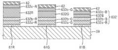
도 8을 참조하면, 도 6의 증착 장치를 이용하여 제조된 유기 발광 디스플레이 장치는, 화소전극(61R, 61G, 61B), 중간층(632), 대향전극(62)을 포함한다. 그리고, 중간층(632)은 각 부화소 별로 패터닝되어 형성된다.Referring to FIG. 8, an organic light emitting display device manufactured using the deposition apparatus of FIG. 6 includes
즉, 적색 부화소에는 홀 주입층(632a-R), 홀 수송층(632b-R), 적색 발광층(632R), 전자 수송층(632c-R)이 차례로 패터닝되어 적층 형성된다. 한편, 녹색 부화소에는 홀 주입층(632a-R), 홀 수송층(632b-G), 녹색 발광층(632G), 전자 수송층(632c-G)이 차례로 패터닝되어 적층 형성된다. 한편, 청색 부화소에는 홀 주입층(632a-B), 홀 수송층(632b-B), 청색 발광층(632B), 전자 수송층(632c-B)이 차례로 패터닝되어 적층 형성된다. 그리고, 중간층(632)을 덮도록 대향전극(62)이 공통층으로 형성된다. (도 8은 부화소와 부화소 사이의 공간을 생략하여 도시하였기 때문에, 대향전극(62)이 패턴층인 것으로 보일 수 있으나, 대향전극(62)은 공통층으로 형성된다.)That is, a
이와 같은 중간층(631)의 증착 방법은 다음과 같다.The deposition method of the
패턴층 증착용 마스크 어셈블리(620)는 마스크 트레이(621), 마스크(622) 및 마그넷 플레이트(623)를 포함하고, 이때 마스크(622)는 복수 개의 슬릿이 형성된 패턴 마스크 형태이므로, 패턴층 증착용 마스크 어셈블리(620)에 결합된 기판(500)이 증착 어셈블리(100-1', ... , 100-11')를 통과하면서, 기판(500) 상에 패턴층이 형성된다.The pattern layer
즉, 첫 번째 스캔시, 기판(500)이 제1 증착 어셈블리(100-1')와 제2 증착 어셈블리(100-2')를 지나면서 기판(500) 상에 홀 주입층(632a-R)이 형성되고, 제3 증착 어셈블리(100-3')와 제4 증착 어셈블리(100-4')와 제5 증착 어셈블리(100-5')를 지나면서 기판(500) 상에 홀 수송층(632b-R)이 형성되고, 제6 증착 어셈블리(100-6')를 지나면서 기판(500) 상에 적색 발광층(632R)이 형성되고, 제9 증착 어셈블리(100-9')와 제10 증착 어셈블리(100-10')를 지나면서 기판(500) 상에 전자 수송층(632c-R)이 형성된다. 이때, 증착된 모든 층은 패턴층 형태로 형성되어 적색 부화소 상에 적층된다. 이때, 제2 차단 부재(122)는 녹색 발광층을 증착하는 제7 증착 어셈블리(100-7')와 기판(500) 사이에 형성되어 녹색 발광물질이 기판(500)에 증착되지 아니하도록 하며, 제3 차단 부재(123)는 청색 발광층을 증착하는 제8 증착 어셈블리(100-8')와 기판(500) 사이에 형성되어 청색 발광물질이 기판(500)에 증착되지 아니하도록 한다.That is, during the first scan, the
제1회의 스캔 증착을 마친 패턴층 증착용 마스크 어셈블리(620)(및 이와 결합된 기판(500))은 제2 이송부(도 2의 420)에 의해 로딩부(200)로 회송된다. 그리고나서, 패턴층 증착용 마스크 어셈블리(620)는 기판(500)에 대해 일정 정도 오프셋(offset) 된다. 이는 다음 패턴층의 형성을 위함이다.The pattern layer deposition mask assembly 620 (and the
마찬가지 방법으로, 두 번째 스캔시, 기판(500)이 증착 어셈블리(100-1', ... , 100-11')를 지나면서 기판(500) 상에 홀 주입층(632a-G), 홀 수송층(632b-G), 녹색 발광층(632G) 및 전자 수송층(632c-G)이 형성된다. 이때, 증착된 모든 층은 패턴층 형태로 녹색 부화소 상에 적층 형성되며, 이때 형성된 중간층은 첫 번째 스캔시 형성된 중간층으로부터 일정 정도 평행이동된 위치에 형성된다. 이때, 제1 차단 부재(121)는 적색 발광층을 증착하는 제6 증착 어셈블리(100-6')와 기판(500) 사이에 형성되어 적색 발광물질이 기판(500)에 증착되지 아니하도록 하며, 제3 차단 부재(123)는 청색 발광층을 증착하는 제8 증착 어셈블리(100-8')와 기판(500) 사이에 형성되어 청색 발광물질이 기판(500)에 증착되지 아니하도록 한다.In the same way, in the second scan, the
제2회의 스캔 증착을 마친 패턴층 증착용 마스크 어셈블리(620)(및 이와 결합된 기판(500))은 제2 이송부(도 2의 420)에 의해 로딩부(200)로 회송된다. 그리고나서, 패턴층 증착용 마스크 어셈블리(620)는 기판(500)에 대해 일정 정도 오프셋(offset) 된다. 이는 다음 패턴층의 형성을 위함이다.The pattern layer deposition mask assembly 620 (and the
마찬가지 방법으로, 세 번째 스캔시, 기판(500)이 증착 어셈블리(100-1', ... , 100-11')를 지나면서 기판(500) 상에 홀 주입층(632a-B), 홀 수송층(632b-B), 청색 발광층(632B) 및 전자 수송층(632c-B)이 형성된다. 이때, 증착된 모든 층은 패턴층 형태로 청색 부화소 상에 적층 형성되며, 이때 형성된 중간층은 첫 번째 및 두 번째 스캔시 형성된 중간층으로부터 일정 정도 평행이동된 위치에 형성된다. 이때, 제1 차단 부재(121)는 적색 발광층을 증착하는 제6 증착 어셈블리(100-6')와 기판(500) 사이에 형성되어 적색 발광물질이 기판(500)에 증착되지 아니하도록 하며, 제2 차단 부재(122)는 녹색 발광층을 증착하는 제7 증착 어셈블리(100-8')와 기판(500) 사이에 형성되어 녹색 발광물질이 기판(500)에 증착되지 아니하도록 한다.In the same way, in the third scan, the
이와 같이 패턴층 증착용 마스크 어셈블리(620)만을 사용하여 복수 회의 스캔으로 복수의 부화소들에 각각 적색, 녹색 및 청색의 빛을 방출하는 유기 발광층을 구비하는 중간층을 형성함으로써, RGB 방식의 유기 발광 디스플레이 장치를 제조할 수 있는 것이다.
As described above, by forming an intermediate layer including an organic emission layer emitting red, green, and blue light on a plurality of subpixels through a plurality of scans using only the pattern layer
도 9는 도 1의 증착부의 다른 일 실시예를 개략적으로 도시한 사시도이다.9 is a perspective view schematically showing another embodiment of the deposition unit of FIG. 1.
도 9에 도시된 본 발명의 다른 일 실시예에 따른 증착 장치의 증착부(100'')에서는, 공통층 증착용 마스크 어셈블리(610)와 패턴층 증착용 마스크 어셈블리(620)를 함께 사용하여, 1회의 스캔을 통해 복수의 부화소들이 각각 적색, 녹색 및 청색의 빛을 방출하는 유기 발광층을 구비하는 구조의 RGB 방식의 유기 발광 디스플레이 장치를 제조할 수 있다. 이하에서는 이에 대하여 보다 상세히 설명하도록 한다.In the
도 9를 참조하면, 본 발명의 다른 일 실시예에 관한 증착 장치의 증착부(100'')는 하나 이상의 증착 어셈블리(100-1'', ... , 100-11'')와, 공통층 증착용 마스크 어셈블리(610)와 패턴층 증착용 마스크 어셈블리(620)를 포함한다. 여기서, 공통층 증착용 마스크 어셈블리(610)는 마스크 트레이(611), 마스크(612) 및 마그넷 플레이트(613)를 포함하고, 패턴층 증착용 마스크 어셈블리(620)는 마스크 트레이(621), 마스크(622) 및 마그넷 플레이트(623)를 포함한다. 본 실시예에서, 공통층 증착용 마스크 어셈블리(610)는 도 4에서 설명한 공통층 증착용 마스크 어셈블리와 동일하고, 패턴층 증착용 마스크 어셈블리(620)는 도 6에서 설명한 패턴층 증착용 마스크 어셈블리와 동일하므로, 그 상세한 설명은 생략하도록 한다.Referring to FIG. 9, the
한편, 도 9에 도시된 열한 개의 증착 어셈블리들은 각각 유기 발광 디스플레이 장치의 중간층을 증착하는데 사용될 수 있다.Meanwhile, each of the eleven deposition assemblies shown in FIG. 9 may be used to deposit an intermediate layer of the organic light emitting display device.
열한 개의 증착 어셈블리들의 배열의 일 예로써, 제1 증착 어셈블리(100-1'')와 제2 증착 어셈블리(100-2'')는 홀 주입층(HIL: Hole Injection Layer)용 증착 물질을 구비하고, 제3 증착 어셈블리(100-3'')와 제4 증착 어셈블리(100-4'')와 제5 증착 어셈블리(100-5'')는 홀 수송층(HTL: Hole Transport Layer)용 증착 물질을 구비하고, 제6 증착 어셈블리(100-6'')는 적색 발광층용 증착 물질을 구비하고, 제7 증착 어셈블리(100-7'')는 녹색 발광층용 증착 물질을 구비하고, 제8 증착 어셈블리(100-8'')는 청색 발광층용 증착 물질을 구비하고, 제9 증착 어셈블리(100-9'')와 제10 증착 어셈블리(100-10'')는 전자 수송층(ETL: Electron Transport Layer)용 증착 물질을 구비하고, 제11 증착 어셈블리(100-11'')는 전자 주입층(EIL: Electron Injection Layer)용 증착 물질을 구비하도록 배치될 수 있다. 물론 이와 같은 증착 어셈블리들의 배열은 다양하게 변경 가능하다 할 것이다. 또한, 증착에 사용되지 않는 증착 어셈블리에는 증착 물질이 채워져 있지 않을 수도 있다.As an example of an arrangement of eleven deposition assemblies, the first deposition assembly 100-1'' and the second deposition assembly 100-2'' are provided with a deposition material for a hole injection layer (HIL). And, the third deposition assembly (100-3''), the fourth deposition assembly (100-4'') and the fifth deposition assembly (100-5'') are a deposition material for a hole transport layer (HTL). And, the sixth deposition assembly (100-6'') is provided with a deposition material for a red light-emitting layer, the seventh deposition assembly (100-7″) is provided with a deposition material for a green light-emitting layer, and the eighth deposition assembly (100-8``) is provided with a deposition material for a blue light emitting layer, the ninth deposition assembly (100-9'') and the 10th deposition assembly (100-10'') is an electron transport layer (ETL) A deposition material may be provided, and the eleventh deposition assembly 100-11 ″ may be disposed to include a deposition material for an electron injection layer (EIL). Of course, the arrangement of such deposition assemblies can be variously changed. Further, a deposition material may not be filled in a deposition assembly that is not used for deposition.
여기서, 도 9에 도시된 본 발명의 일 실시예에 따른 증착 장치를 이용하여, 공통층 증착용 마스크 어셈블리(610)와 패턴층 증착용 마스크 어셈블리(620)를 함께 사용하여 복수의 부화소들이 각각 적색, 녹색 및 청색의 빛을 방출하는 부화소들을 구비는 RGB 방식의 유기 발광 디스플레이 장치를 제조할 수 있다.Here, by using the deposition apparatus according to the embodiment of the present invention shown in FIG. 9, a plurality of subpixels are respectively formed by using the common layer
도 10은 도 9의 증착 장치를 이용하여 제조된 유기 발광 디스플레이 장치의 중간층을 상세히 나타내는 단면도이다.10 is a cross-sectional view illustrating in detail an intermediate layer of an organic light emitting display device manufactured using the deposition apparatus of FIG. 9.
도 10을 참조하면, 도 9의 증착 장치를 이용하여 제조된 유기 발광 디스플레이 장치는, 화소전극(61R, 61G, 61B), 중간층(633), 대향전극(62)을 포함한다. 그리고, 중간층(633)은 홀 주입층(633a), 홀 수송층(633b), 적색 발광층(633R), 녹색 발광층(633G), 청색 발광층(633B), 전자 수송층(633c)을 포함한다.Referring to FIG. 10, the organic light emitting display device manufactured using the deposition apparatus of FIG. 9 includes
이때, 중간층(633) 중 발광층(633R, 633G, 633B)은 각 부화소 별로 패터닝되어 형성되고, 홀 주입층(633a), 홀 수송층(633b), 전자 수송층(633c)은 공통층으로 형성된다. 이와 같은 중간층(633)의 증착 방법은 다음과 같다.In this case, the
공통층 증착용 마스크 어셈블리(610)는 마스크 트레이(611), 마스크(612) 및 마그넷 플레이트(613)를 포함하고, 이때 마스크(612)는 오픈 마스크 형태이므로, 공통층 증착용 마스크 어셈블리(610)에 결합된 기판(500)이 증착 어셈블리를 통과하면서, 기판(500) 상에 공통층이 증착된다.The common layer
한편, 패턴층 증착용 마스크 어셈블리(620)는 마스크 트레이(621), 마스크(622) 및 마그넷 플레이트(623)를 포함하고, 이때 마스크(622)는 복수 개의 슬릿이 형성된 패턴 마스크 형태이므로, 패턴층 증착용 마스크 어셈블리(620)에 결합된 기판(500)이 증착 어셈블리를 통과하면서, 기판(500) 상에 패턴층이 형성된다.Meanwhile, the
먼저, 기판(500)이 공통층 증착용 마스크 어셈블리(610)와 결합한 상태에서 증착이 시작된다. 즉, 기판(500)이 제1 증착 어셈블리(100-1'')와 제2 증착 어셈블리(100-2'')를 지나면서 기판(500) 상에 홀 주입층(633a)이 형성되고, 제3 증착 어셈블리(100-3'')와 제4 증착 어셈블리(100-4'')와 제5 증착 어셈블리(100-5'')를 지나면서 기판(500) 상에 홀 수송층(633b)이 형성된다. 이때 홀 주입층(633a)과 홀 수송층(633b)은 공통층 형태로 형성되어 적층된다.First, deposition is started in a state in which the
이 상태에서, 기판(500)을 공통층 증착용 마스크 어셈블리(610)와 분리한 후, 패턴층 증착용 마스크 어셈블리(620)와 결합한다. 그리고나서, 기판(500)이 제6 증착 어셈블리(100-6'')를 지나면서 기판(500) 상의 적색 부화소에 적색 발광층(633R)이 형성된다. 그리고나서 패턴층 증착용 마스크 어셈블리(620)는 기판(500)에 대해 일정 정도 오프셋(offset) 된다. 즉, 다음 패턴층의 형성을 위해, 패턴층 증착용 마스크 어셈블리(620)는 기판(500)에 대해 일정 정도 평행이동 하는 것이다. 그리고나서, 기판(500)이 제7 증착 어셈블리(100-7'')를 지나면서 기판(500)의 녹색 부화소 상에 녹색 발광층(633G)이 형성된다. 그리고 나서 패턴층 증착용 마스크 어셈블리(620)는 기판(500)에 대해 일정 정도 오프셋(offset) 된다. 그리고나서, 기판(500)이 제8 증착 어셈블리(100-8'')를 지나면서 기판(500) 상의 청색 부화소에 청색 발광층(633B)이 형성된다. 이때, 적색 발광층(633R), 녹색 발광층(633G), 청색 발광층(633B)은 패턴층 형태로 각 부화소에 형성된다.In this state, the
이 상태에서, 기판(500)을 패턴층 증착용 마스크 어셈블리(620)와 분리한 후, 공통층 증착용 마스크 어셈블리(610)와 결합한다. 그리고나서, 기판(500)이 제9 증착 어셈블리(100-9'')와 제10 증착 어셈블리(100-10'')를 지나면서 기판(500) 상에 전자 수송층(633c)이 형성된다. 이때 전자 수송층(633c)은 공통층 형태로 형성되어 적층된다.In this state, the
이와 같이 공통층 증착용 마스크 어셈블리(610)와 패턴층 증착용 마스크 어셈블리(620)를 함께 사용함으로써, 1회의 스캔만으로 복수의 부화소들에 각각 적색, 녹색 및 청색의 빛을 방출하는 유기 발광층을 구비하는 중간층을 형성함으로써, RGB 방식의 유기 발광 디스플레이 장치를 제조할 수 있는 것이다.
As described above, by using the common layer
도 11은 본 발명의 다른 일 실시예에 따른 증착 장치를 이용하여 제조된 유기 발광 디스플레이 장치의 중간층의 다른 일 예를 나타내는 단면도이다. 본 실시예에서는 패턴층 증착용 마스크 어셈블리만을 사용하여, 여러 번의 스캔을 통해 복수의 부화소들이 각각 적색, 녹색, 청색 및 백색의 빛을 방출하는 RGBW 방식의 유기 발광 디스플레이 장치를 제조할 수 있다.11 is a cross-sectional view illustrating another example of an intermediate layer of an organic light emitting display device manufactured using a deposition apparatus according to another embodiment of the present invention. In the present embodiment, it is possible to manufacture an RGBW type organic light-emitting display device in which a plurality of subpixels emit red, green, blue, and white light through multiple scans by using only the pattern layer deposition mask assembly.
도 11을 참조하면, 본 실시예에 따른 유기 발광 디스플레이 장치는, 화소전극(61R, 61G, 61B), 중간층(634), 대향전극(62)을 포함한다. 그리고, 중간층(634)은 각 부화소 별로 패터닝되어 형성된다.Referring to FIG. 11, the organic light emitting display device according to the present embodiment includes
즉, 적색 부화소에는 홀 주입층(634a-R), 홀 수송층(634b-R), 적색 발광층(634R), 전자 수송층(634c-R)이 차례로 패터닝되어 적층 형성된다. 한편, 녹색 부화소에는 홀 주입층(634a-R), 홀 수송층(634b-G), 녹색 발광층(634G), 전자 수송층(634c-G)이 차례로 패터닝되어 적층 형성된다. 한편, 청색 부화소에는 홀 주입층(634a-B), 홀 수송층(634b-B), 청색 발광층(634B), 전자 수송층(634c-B)이 차례로 패터닝되어 적층 형성된다. 한편, 백색 부화소에는 홀 수송층(634d-W), 청색 발광층(634e-W), 전하 생성층(634f-W), 적색 발광층(634g-W), 녹색 발광층(634h-W), 전자 수송층(634i-W)을 차례로 패터닝되어 적층 형성된다. 그리고, 중간층(632)을 덮도록 대향전극(62)이 공통층으로 형성된다.That is, a
이와 같이 패턴층 증착용 마스크 어셈블리만을 사용하여 복수 회의 스캔으로 복수의 부화소들에 각각 적색, 녹색, 청색 및 백색의 빛을 방출하는 중간층을 형성함으로써, RGBW 방식의 유기 발광 디스플레이 장치를 제조할 수 있는 것이다.In this way, by forming an intermediate layer that emits red, green, blue, and white light on a plurality of subpixels through a plurality of scans using only the pattern layer deposition mask assembly, an RGBW type organic light emitting display device can be manufactured. will be.
이와 같은 본 발명에 의해서, 대형 유기 발광 디스플레이 장치에 대한 유연한 증착 공정을 적용할 수 있게 된다. 즉, 하나의 증착 장치를 이용하여, RGB 방식, RGBW 방식 또는 white OLED 방식의 유기 발광 디스플레이 장치를 선택적으로 제조할 수 있게 됨으로써, 유연한 설비 운용이 가능해지는 효과를 얻을 수 있다. 또한 클러스터 타입의 종래의 증착 장치에 비해, 설비의 레이아웃(layout)이 축소되어, 공간 활용성이 높아지는 효과를 얻을 수 있으며, 인라인 설비의 적용에 의해 공정 시간이 단축되는 효과를 얻을 수 있다.According to the present invention as described above, a flexible deposition process can be applied to a large organic light emitting display device. That is, by using a single deposition apparatus, it is possible to selectively manufacture an organic light-emitting display device of an RGB method, an RGBW method, or a white OLED method, thereby obtaining an effect of enabling flexible facility operation. In addition, compared to the conventional deposition apparatus of the cluster type, the layout of the facility is reduced, so that the space utilization is increased, and the process time can be shortened by the application of the in-line facility.
이와 같이 본 발명은 도면에 도시된 일 실시예를 참고로 하여 설명하였으나 이는 예시적인 것에 불과하며 당해 분야에서 통상의 지식을 가진 자라면 이로부터 다양한 변형 및 실시예의 변형이 가능하다는 점을 이해할 것이다. 따라서, 본 발명의 진정한 기술적 보호 범위는 첨부된 특허청구범위의 기술적 사상에 의하여 정해져야 할 것이다.As described above, the present invention has been described with reference to an embodiment shown in the drawings, but this is only exemplary, and those of ordinary skill in the art will understand that various modifications and variations of the embodiment are possible therefrom. Therefore, the true technical scope of the present invention should be determined by the technical spirit of the appended claims.
1: 증착 장치
100: 증착부
200: 로딩부
300: 언로딩부
400: 이송부
610: 공통층 증착용 마스크 어셈블리
611: 마스크 트레이
612: 마스크
613: 마그넷 플레이트
620: 패턴층 증착용 마스크 어셈블리
621: 마스크 트레이
622: 마스크
623: 마그넷 플레이트1: evaporation device
100: evaporation unit
200: loading part
300: unloading unit
400: transfer unit
610: common layer deposition mask assembly
611: mask tray
612: mask
613: magnet plate
620: pattern layer deposition mask assembly
621: mask tray
622: mask
623: magnet plate
Claims (20)
Translated fromKorean로딩부에서 상기 기판을 공통층 증착용 마스크 어셈블리 또는 패턴층 증착용 마스크 어셈블리에 고정시키는 단계;
증착부 내에 배치된 하나 이상의 증착 어셈블리와 상기 공통층 증착용 마스크 어셈블리 또는 패턴층 증착용 마스크 어셈블리에 고정된 상기 기판이 소정 정도 이격된 상태에서, 제1 이송부에 의해 상기 기판이 상기 증착 어셈블리에 대해 상대적으로 이동하면서 상기 증착 어셈블리로부터 발산된 증착 물질이 상기 기판에 증착되어 중간층이 형성되는 단계; 및
언로딩부에서 증착이 완료된 상기 기판을 상기 공통층 증착용 마스크 어셈블리 또는 패턴층 증착용 마스크 어셈블리로부터 분리시키는 단계;를 포함하는 유기 발광 디스플레이 장치의 제조 방법.In the manufacturing method of an organic light emitting display device using a vapor deposition device for forming an organic layer on a substrate,
Fixing the substrate to a common layer deposition mask assembly or a pattern layer deposition mask assembly in a loading unit;
In a state where at least one deposition assembly disposed in the deposition unit and the substrate fixed to the common layer deposition mask assembly or the pattern layer deposition mask assembly are spaced apart by a predetermined degree, the substrate is moved to the deposition assembly by a first transfer unit. Depositing a deposition material emanating from the deposition assembly while moving relatively to the substrate to form an intermediate layer; And
Separating the substrate, which has been deposited by an unloading unit, from the common layer deposition mask assembly or the pattern layer deposition mask assembly.
상기 로딩부에서 상기 기판이 상기 공통층 증착용 마스크 어셈블리에 고정되고,
상기 기판상에는 상기 증착 물질이 공통층으로 형성되는 것을 특징으로 하는 유기 발광 디스플레이 장치의 제조 방법.The method of claim 1,
In the loading part, the substrate is fixed to the common layer deposition mask assembly,
The method of manufacturing an organic light emitting display device, wherein the deposition material is formed as a common layer on the substrate.
상기 중간층이 형성되는 단계는,
상기 기판상에 적어도 적색 발광층, 녹색 발광층, 청색 발광층이 공통층으로 적층되는 것을 특징으로 하는 유기 발광 디스플레이 장치의 제조 방법.The method of claim 2,
The step of forming the intermediate layer,
A method of manufacturing an organic light-emitting display device, wherein at least a red emission layer, a green emission layer, and a blue emission layer are stacked on the substrate as a common layer.
상기 로딩부에서 상기 기판이 상기 패턴층 증착용 마스크 어셈블리에 고정되고,
상기 기판상에는 상기 증착 물질이 소정의 형상으로 패터닝되어 형성되는 것을 특징으로 하는 유기 발광 디스플레이 장치의 제조 방법.The method of claim 1,
In the loading part, the substrate is fixed to the pattern layer deposition mask assembly,
The method of manufacturing an organic light emitting display device, wherein the deposition material is formed by patterning the deposition material in a predetermined shape on the substrate.
상기 중간층이 형성되는 단계는,
상기 기판상에 적색 발광층, 녹색 발광층, 청색 발광층이 각각 패턴층으로 형성되는 것을 특징으로 하는 유기 발광 디스플레이 장치의 제조 방법.The method of claim 4,
The step of forming the intermediate layer,
A method of manufacturing an organic light-emitting display device, wherein a red light-emitting layer, a green light-emitting layer, and a blue light-emitting layer are each formed as a pattern layer on the substrate.
상기 공통층 증착용 마스크 어셈블리 또는 패턴층 증착용 마스크 어셈블리가 선택적으로 상기 기판과 결합하는 것을 특징으로 하는 유기 발광 디스플레이 장치의 제조 방법.The method of claim 1,
The method of manufacturing an organic light emitting display device, wherein the common layer deposition mask assembly or the pattern layer deposition mask assembly is selectively coupled to the substrate.
상기 기판이 상기 패턴층 증착용 마스크 어셈블리에 고정된 상태에서 상기 기판이 상기 증착 어셈블리에 대해 상대적으로 이동하면서 상기 기판상에 어느 하나의 발광층이 증착되는 단계;
상기 기판이 고정된 상기 패턴층 증착용 마스크 어셈블리가 회송되는 단계;
상기 기판이 상기 증착 어셈블리에 대해 상대적으로 이동하면서 상기 기판상에 다른 하나의 발광층이 증착되는 단계;를 포함하는 유기 발광 디스플레이 장치의 제조 방법.The method of claim 1,
Depositing one light-emitting layer on the substrate while the substrate is moved relative to the deposition assembly while the substrate is fixed to the pattern layer deposition mask assembly;
Returning the pattern layer deposition mask assembly to which the substrate is fixed;
And depositing another emission layer on the substrate while the substrate moves relative to the deposition assembly.
하나의 발광층이 증착되는 동안, 다른 발광층용 증착 물질을 구비하는 증착 어셈블리와 기판 사이에는 차단 부재가 형성되는 것을 특징으로 하는 유기 발광 디스플레이 장치의 제조 방법.The method of claim 7,
A method of manufacturing an organic light-emitting display device, wherein a blocking member is formed between a substrate and a deposition assembly including a deposition material for another light-emitting layer while one light-emitting layer is deposited.
상기 기판이 고정된 상기 패턴층 증착용 마스크 어셈블리가 회송된 후,
상기 패턴층 증착용 마스크 어셈블리가 상기 기판에 대해 일정 정도 오프셋되는 단계를 더 포함하는 유기 발광 디스플레이 장치의 제조 방법.The method of claim 7,
After the pattern layer deposition mask assembly to which the substrate is fixed is returned,
The method of manufacturing an organic light emitting display device further comprising the step of offsetting the pattern layer deposition mask assembly with respect to the substrate by a predetermined degree.
상기 중간층이 형성되는 단계는,
상기 기판이 상기 공통층 증착용 마스크 어셈블리에 고정된 상태에서 상기 기판이 상기 증착 어셈블리에 대해 상대적으로 이동하면서 상기 기판상에 하나 이상의 공통층이 증착되는 단계;
상기 기판이 상기 공통층 증착용 마스크 어셈블리로부터 분리되고, 상기 패턴층 증착용 마스크 어셈블리에 고정되는 단계;
상기 기판이 상기 패턴층 증착용 마스크 어셈블리에 고정된 상태에서 상기 기판이 상기 증착 어셈블리에 대해 상대적으로 이동하면서 상기 기판상에 적색 발광층, 녹색 발광층, 청색 발광층이 각각 패터닝 되는 단계;를 포함하는 유기 발광 디스플레이 장치의 제조 방법.The method of claim 1,
The step of forming the intermediate layer,
Depositing at least one common layer on the substrate while the substrate is moved relative to the deposition assembly while the substrate is fixed to the common layer deposition mask assembly;
Separating the substrate from the common layer deposition mask assembly and fixing it to the pattern layer deposition mask assembly;
And patterning a red emission layer, a green emission layer, and a blue emission layer on the substrate while the substrate is fixed to the pattern layer deposition mask assembly while the substrate moves relative to the deposition assembly. Method of manufacturing a display device.
상기 기판상에 발광층이 패터닝 되는 단계는,
상기 기판상에 하나의 발광층이 패터닝된 후, 상기 패턴층 증착용 마스크 어셈블리가 상기 기판에 대해 일정 정도 오프셋되는 단계를 포함하는 유기 발광 디스플레이 장치의 제조 방법.The method of claim 10,
The step of patterning the light emitting layer on the substrate,
And after one light emitting layer is patterned on the substrate, the pattern layer deposition mask assembly is offset to the substrate by a certain degree.
상기 기판상에 발광층이 패터닝 되는 단계 이후,
상기 기판이 상기 패턴층 증착용 마스크 어셈블리로부터 분리되고, 상기 공통층 증착용 마스크 어셈블리에 고정되는 단계;
상기 기판이 상기 공통층 증착용 마스크 어셈블리에 고정된 상태에서 상기 기판이 상기 증착 어셈블리에 대해 상대적으로 이동하면서 상기 기판상에 하나 이상의 공통층이 증착되는 단계;를 더 포함하는 유기 발광 디스플레이 장치의 제조 방법.The method of claim 10,
After the step of patterning the light emitting layer on the substrate,
Separating the substrate from the pattern layer deposition mask assembly and fixing the substrate to the common layer deposition mask assembly;
The manufacturing of an organic light emitting display device further comprising: depositing one or more common layers on the substrate while the substrate is moved relative to the deposition assembly while the substrate is fixed to the common layer deposition mask assembly. Way.
상기 중간층이 형성되는 단계는,
상기 기판상의 어느 한가지 색을 방출하는 부화소 영역에 적어도 발광층을 포함하는 하나 이상의 중간층이 차례로 적층되어 형성되는 단계;
상기 기판상의 다른 색을 방출하는 부화소 영역에 적어도 발광층을 포함하는 하나 이상의 중간층이 차례로 적층되어 형성되는 단계; 및
상기 기판상의 또 다른 색을 방출하는 부화소 영역에 적어도 발광층을 포함하는 하나 이상의 중간층이 차례로 적층되어 형성되는 단계;를 포함하는 유기 발광 디스플레이 장치의 제조 방법.The method of claim 1,
The step of forming the intermediate layer,
Forming one or more intermediate layers including at least an emission layer sequentially stacked in a subpixel region emitting any one color on the substrate;
Forming one or more intermediate layers including at least an emission layer sequentially stacked in a subpixel area emitting different colors on the substrate; And
And forming one or more intermediate layers including at least an emission layer sequentially stacked in a subpixel area emitting another color on the substrate.
상기 단계들 이후에,
상기 기판상의 또 다른 부화소 영역에, 적색 발광층, 녹색 발광층, 청색 발광층이 적층 형성되는 단계를 더 포함하는 유기 발광 디스플레이 장치의 제조 방법.The method of claim 13,
After the above steps,
The method of manufacturing an organic light emitting display device further comprising the step of laminating and forming a red light emitting layer, a green light emitting layer, and a blue light emitting layer in another subpixel area on the substrate.
상기 중간층이 형성되는 단계는,
상기 기판상에 하나 이상의 공통층이 형성되는 단계;
상기 기판상에 각각의 부화소 영역에 각각의 발광층들이 차례로 패터닝되는 단계; 및
상기 기판상에 하나 이상의 공통층이 형성되는 단계;를 포함하는 유기 발광 디스플레이 장치의 제조 방법.The method of claim 1,
The step of forming the intermediate layer,
Forming one or more common layers on the substrate;
Sequentially patterning each of the light emitting layers in each subpixel area on the substrate; And
The method of manufacturing an organic light emitting display device comprising: forming one or more common layers on the substrate.
상기 공통층 증착용 마스크 어셈블리 또는 패턴층 증착용 마스크 어셈블리가 제2 이송부를 이용하여 회송되는 단계를 더 포함하는 유기 발광 디스플레이 장치의 제조 방법.The method of claim 1,
The method of manufacturing an organic light emitting display device further comprising the step of returning the common layer deposition mask assembly or the pattern layer deposition mask assembly using a second transfer unit.
상기 공통층 증착용 마스크 어셈블리 또는 패턴층 증착용 마스크 어셈블리는 상기 제1 이송부와 상기 제2 이송부 사이를 순환하는 것을 특징으로 하는 유기 발광 디스플레이 장치의 제조 방법.The method of claim 16,
The method of manufacturing an organic light-emitting display device, wherein the common layer deposition mask assembly or the pattern layer deposition mask assembly circulates between the first transfer unit and the second transfer unit.
상기 공통층 증착용 마스크 어셈블리 또는 패턴층 증착용 마스크 어셈블리는 각각,
하나 이상의 개구부가 형성되어 기판의 증착 영역을 정의하는 마스크;
일면 상에 상기 마스크가 안착되는 마스크 트레이; 및
상기 기판에서 상기 마스크와 접촉하는 면의 반대측 면에 형성되어 상기 마스크에 소정의 자기력을 가하는 마그넷 플레이트;를 포함하는 유기 발광 디스플레이 장치의 제조 방법.The method of claim 1,
Each of the common layer deposition mask assembly or pattern layer deposition mask assembly,
A mask having one or more openings formed therein to define a deposition area of the substrate;
A mask tray on which the mask is mounted on one side; And
And a magnet plate formed on a surface opposite to a surface of the substrate in contact with the mask to apply a predetermined magnetic force to the mask.
상기 마그넷 플레이트는 상기 마스크를 상기 마그넷 플레이트 쪽으로 당기는 방향으로 자기력을 발생시키는 것을 특징으로 하는 유기 발광 디스플레이 장치의 제조 방법.The method of claim 18,
Wherein the magnet plate generates a magnetic force in a direction pulling the mask toward the magnet plate.
상기 증착부 내부에 복수의 증착 어셈블리들이 구비되어 각 증착 어셈블리들에 의해 상기 기판에 연속적으로 증착이 이루어지는 유기 발광 디스플레이 장치의 제조 방법.The method of claim 1,
A method of manufacturing an organic light emitting display device in which a plurality of deposition assemblies are provided inside the deposition unit to continuously deposit the substrate by the deposition assemblies.
Priority Applications (3)
| Application Number | Priority Date | Filing Date | Title |
|---|---|---|---|
| KR1020130161780AKR102162797B1 (en) | 2013-12-23 | 2013-12-23 | Method for manufacturing of organic light emitting display apparatus |
| US14/295,245US9496317B2 (en) | 2013-12-23 | 2014-06-03 | Method of manufacturing organic light emitting display apparatus |
| CN201410690142.5ACN104733496B (en) | 2013-12-23 | 2014-11-25 | Method of manufacturing organic light emitting display device |
Applications Claiming Priority (1)
| Application Number | Priority Date | Filing Date | Title |
|---|---|---|---|
| KR1020130161780AKR102162797B1 (en) | 2013-12-23 | 2013-12-23 | Method for manufacturing of organic light emitting display apparatus |
Publications (2)
| Publication Number | Publication Date |
|---|---|
| KR20150073743A KR20150073743A (en) | 2015-07-01 |
| KR102162797B1true KR102162797B1 (en) | 2020-10-08 |
Family
ID=53400947
Family Applications (1)
| Application Number | Title | Priority Date | Filing Date |
|---|---|---|---|
| KR1020130161780AActiveKR102162797B1 (en) | 2013-12-23 | 2013-12-23 | Method for manufacturing of organic light emitting display apparatus |
Country Status (3)
| Country | Link |
|---|---|
| US (1) | US9496317B2 (en) |
| KR (1) | KR102162797B1 (en) |
| CN (1) | CN104733496B (en) |
Families Citing this family (6)
| Publication number | Priority date | Publication date | Assignee | Title |
|---|---|---|---|---|
| US9496524B2 (en) | 2012-07-10 | 2016-11-15 | Samsung Display Co., Ltd. | Organic layer deposition apparatus, method of manufacturing organic light-emitting display apparatus using the same, and organic light-emitting display apparatus manufactured using the method |
| KR102211964B1 (en)* | 2013-08-22 | 2021-02-05 | 삼성디스플레이 주식회사 | Thin film depositing apparatus and the thin film depositing method using the same |
| KR102356353B1 (en)* | 2015-07-07 | 2022-01-27 | 삼성디스플레이 주식회사 | Deposition device and method of manufacturing display device using the same |
| KR102615639B1 (en) | 2016-09-26 | 2023-12-20 | 삼성디스플레이 주식회사 | organic light emitting display device, mask for fabricating the same, and the fabrication method thereof |
| KR102618039B1 (en) | 2018-08-29 | 2023-12-27 | 삼성디스플레이 주식회사 | Mask assembly, apparatus and method for manufacturing a display apparatus having the same |
| WO2020164687A1 (en)* | 2019-02-12 | 2020-08-20 | Applied Materials, Inc. | Holder for substrate processing in a vacuum chamber, holding arrangement, system and method |
Family Cites Families (159)
| Publication number | Priority date | Publication date | Assignee | Title |
|---|---|---|---|---|
| JPS5959237U (en) | 1982-10-15 | 1984-04-18 | 鐘通工業株式会社 | Switchable permanent magnetic chuck |
| JP3125279B2 (en) | 1991-02-25 | 2001-01-15 | 東海カーボン株式会社 | Graphite crucible for vacuum evaporation |
| JP2572861Y2 (en) | 1991-05-13 | 1998-05-25 | テイエチケー株式会社 | Slide unit for linear motion |
| JP2534431Y2 (en) | 1991-08-30 | 1997-04-30 | 大日本スクリーン製造株式会社 | Substrate transfer device |
| KR0151312B1 (en) | 1995-07-27 | 1998-10-15 | 배순훈 | Anti-direction feeding apparatus of supplying parts of battery |
| CH691680A5 (en) | 1996-10-15 | 2001-09-14 | Unaxis Deutschland Gmbh | Transport apparatus for workpieces in a vacuum system. |
| US6274198B1 (en) | 1997-02-24 | 2001-08-14 | Agere Systems Optoelectronics Guardian Corp. | Shadow mask deposition |
| KR100257219B1 (en) | 1997-10-23 | 2000-05-15 | 박용관 | Method and device for making a safety operation of a polyethylene gas pipe valve arrangement |
| JP2000068054A (en) | 1998-08-26 | 2000-03-03 | Hokuriku Electric Ind Co Ltd | Manufacture of el element |
| KR20000019254A (en) | 1998-09-08 | 2000-04-06 | 석창길 | Device for improving thin film thickness uniformity of cvd |
| JP2001028325A (en) | 1999-07-13 | 2001-01-30 | Tdk Corp | Method and device for transfer chip part, and electrode- forming device |
| JP2001052862A (en) | 1999-08-04 | 2001-02-23 | Hokuriku Electric Ind Co Ltd | Manufacture of organic el element and device therefor |
| JP4187367B2 (en) | 1999-09-28 | 2008-11-26 | 三洋電機株式会社 | ORGANIC LIGHT EMITTING ELEMENT, ITS MANUFACTURING DEVICE, AND ITS MANUFACTURING METHOD |
| KR100302159B1 (en) | 1999-10-29 | 2001-09-22 | 최중호 | Scent diffusion apparatus and method therefor |
| WO2001030404A1 (en) | 1999-10-29 | 2001-05-03 | E. One Co., Ltd. | Scent diffusion apparatus and method thereof |
| TW490714B (en) | 1999-12-27 | 2002-06-11 | Semiconductor Energy Lab | Film formation apparatus and method for forming a film |
| KR100653515B1 (en) | 1999-12-30 | 2006-12-04 | 주식회사 팬택앤큐리텔 | Terminal of mobile communication system |
| KR20020000201A (en) | 2000-06-23 | 2002-01-05 | 최승락 | Method cleaning Liquid Chrystal Display using Laser and Vapor Phase |
| JP2002175878A (en) | 2000-09-28 | 2002-06-21 | Sanyo Electric Co Ltd | Layer forming method and color light emitting device manufacturing method |
| US6468496B2 (en) | 2000-12-21 | 2002-10-22 | Arco Chemical Technology, L.P. | Process for producing hydrogen peroxide |
| KR100625403B1 (en) | 2000-12-22 | 2006-09-18 | 주식회사 하이닉스반도체 | Virtual Channel SDRAM |
| KR100698033B1 (en) | 2000-12-29 | 2007-03-23 | 엘지.필립스 엘시디 주식회사 | Organic electroluminescent device and manufacturing method thereof |
| KR100405080B1 (en) | 2001-05-11 | 2003-11-10 | 엘지.필립스 엘시디 주식회사 | A method of crystallizing Si |
| KR100463212B1 (en) | 2001-05-19 | 2004-12-23 | 주식회사 아이엠티 | Apparatus for dry surface-cleaning of materials |
| JP2003077662A (en) | 2001-06-22 | 2003-03-14 | Junji Kido | Method and device for manufacturing organic electroluminescent element |
| JP2003003250A (en) | 2001-06-22 | 2003-01-08 | Alps Electric Co Ltd | Vacuum deposition polymerization system and method for depositing organic film using the system |
| KR100406059B1 (en) | 2001-06-22 | 2003-11-17 | 미래산업 주식회사 | Transfer for Tray Feeder |
| US6483690B1 (en) | 2001-06-28 | 2002-11-19 | Lam Research Corporation | Ceramic electrostatic chuck assembly and method of making |
| JP3705237B2 (en) | 2001-09-05 | 2005-10-12 | ソニー株式会社 | Display device manufacturing system and method using organic electroluminescent element |
| KR100446467B1 (en)* | 2001-09-22 | 2004-08-30 | 네오뷰코오롱 주식회사 | Method for manufacturing flat panel display device using supplementary mask |
| TW591202B (en) | 2001-10-26 | 2004-06-11 | Hermosa Thin Film Co Ltd | Dynamic film thickness control device/method and ITS coating method |
| KR100430336B1 (en) | 2001-11-16 | 2004-05-03 | 정광호 | Apparatus for manufacturing organic electro-luminescent light emitting devices for mass production |
| KR100450978B1 (en) | 2001-11-26 | 2004-10-02 | 주성엔지니어링(주) | electrostatic chuck |
| US20030101937A1 (en) | 2001-11-28 | 2003-06-05 | Eastman Kodak Company | Thermal physical vapor deposition source for making an organic light-emitting device |
| US20030168013A1 (en) | 2002-03-08 | 2003-09-11 | Eastman Kodak Company | Elongated thermal physical vapor deposition source with plural apertures for making an organic light-emitting device |
| JP2003297562A (en) | 2002-03-29 | 2003-10-17 | Sanyo Electric Co Ltd | Vapor deposition method |
| US6749906B2 (en) | 2002-04-25 | 2004-06-15 | Eastman Kodak Company | Thermal physical vapor deposition apparatus with detachable vapor source(s) and method |
| US20030232563A1 (en) | 2002-05-09 | 2003-12-18 | Isao Kamiyama | Method and apparatus for manufacturing organic electroluminescence device, and system and method for manufacturing display unit using organic electroluminescence devices |
| JP4030350B2 (en) | 2002-05-28 | 2008-01-09 | 株式会社アルバック | Split electrostatic chuck |
| JP4292777B2 (en) | 2002-06-17 | 2009-07-08 | ソニー株式会社 | Thin film forming equipment |
| US6955726B2 (en) | 2002-06-03 | 2005-10-18 | Samsung Sdi Co., Ltd. | Mask and mask frame assembly for evaporation |
| KR100908232B1 (en) | 2002-06-03 | 2009-07-20 | 삼성모바일디스플레이주식회사 | Mask frame assembly for thin film deposition of organic electroluminescent device |
| MY164487A (en) | 2002-07-11 | 2017-12-29 | Molecular Imprints Inc | Step and repeat imprint lithography processes |
| JP2004043898A (en) | 2002-07-12 | 2004-02-12 | Canon Electronics Inc | Vapor deposition mask, and organic electroluminescence display device |
| KR100397196B1 (en) | 2002-08-27 | 2003-09-13 | 에이엔 에스 주식회사 | Organic material point source feeding unit in organic semiconductor device and method thereof |
| JP2004103269A (en) | 2002-09-05 | 2004-04-02 | Sanyo Electric Co Ltd | Manufacture method for organic electroluminescence display device |
| JP2004103341A (en) | 2002-09-09 | 2004-04-02 | Matsushita Electric Ind Co Ltd | Method for manufacturing organic electroluminescence device |
| US20040123804A1 (en) | 2002-09-20 | 2004-07-01 | Semiconductor Energy Laboratory Co., Ltd. | Fabrication system and manufacturing method of light emitting device |
| JP4139186B2 (en) | 2002-10-21 | 2008-08-27 | 東北パイオニア株式会社 | Vacuum deposition equipment |
| JP2004143521A (en) | 2002-10-24 | 2004-05-20 | Sony Corp | Thin-film deposition device |
| JP2004183044A (en) | 2002-12-03 | 2004-07-02 | Seiko Epson Corp | Mask evaporation method and apparatus, mask and mask manufacturing method, display panel manufacturing apparatus, display panel, and electronic equipment |
| JP2004199919A (en) | 2002-12-17 | 2004-07-15 | Tohoku Pioneer Corp | Method for manufacturing organic el display panel |
| KR100646160B1 (en) | 2002-12-31 | 2006-11-14 | 엘지.필립스 엘시디 주식회사 | Mask for sequential side crystallization and silicon crystallization method using same |
| US20040144321A1 (en) | 2003-01-28 | 2004-07-29 | Eastman Kodak Company | Method of designing a thermal physical vapor deposition system |
| JP3966292B2 (en) | 2003-03-27 | 2007-08-29 | セイコーエプソン株式会社 | Pattern forming method and pattern forming apparatus, device manufacturing method, conductive film wiring, electro-optical device, and electronic apparatus |
| JP2004342455A (en) | 2003-05-15 | 2004-12-02 | Tokki Corp | Flat panel display manufacturing device |
| US6995035B2 (en) | 2003-06-16 | 2006-02-07 | Eastman Kodak Company | Method of making a top-emitting OLED device having improved power distribution |
| KR100832684B1 (en) | 2003-07-08 | 2008-05-27 | 가부시끼가이샤 퓨처 비전 | Substrate stage, electrode used for the substrate stage, and treating apparatus having the substrate stage and the electrode |
| US6837939B1 (en) | 2003-07-22 | 2005-01-04 | Eastman Kodak Company | Thermal physical vapor deposition source using pellets of organic material for making OLED displays |
| JP2005044592A (en) | 2003-07-28 | 2005-02-17 | Toyota Industries Corp | Vapor deposition mask, film formation method using the vapor deposition mask, and film formation apparatus using the vapor deposition mask |
| KR100520159B1 (en) | 2003-11-12 | 2005-10-10 | 삼성전자주식회사 | Apparatus and method for interference cancellation of ofdm system using multiple antenna |
| JP2005213616A (en) | 2004-01-30 | 2005-08-11 | Pioneer Electronic Corp | Vapor deposition method, vapor deposition apparatus and method for manufacturing plasma display panel |
| JP4441282B2 (en) | 2004-02-02 | 2010-03-31 | 富士フイルム株式会社 | Vapor deposition mask and organic EL display device manufacturing method |
| JP2005235568A (en) | 2004-02-19 | 2005-09-02 | Seiko Epson Corp | Vapor deposition apparatus and organic EL device manufacturing method |
| JP2005293968A (en) | 2004-03-31 | 2005-10-20 | Sanyo Electric Co Ltd | Manufacturing method of organic electroluminescent element |
| JP2005296737A (en) | 2004-04-07 | 2005-10-27 | Mikuni Corp | Beat plate |
| JP4455937B2 (en) | 2004-06-01 | 2010-04-21 | 東北パイオニア株式会社 | Deposition source, vacuum film formation apparatus, organic EL panel manufacturing method |
| JP4534011B2 (en)* | 2004-06-25 | 2010-09-01 | 京セラ株式会社 | Display manufacturing method using mask alignment method |
| KR20060008602A (en) | 2004-07-21 | 2006-01-27 | 엘지전자 주식회사 | Organic Electroluminescent Layer Deposition Method |
| KR100579406B1 (en) | 2004-08-25 | 2006-05-12 | 삼성에스디아이 주식회사 | Vertically Moved Organic Material Deposition Equipment |
| KR101070539B1 (en) | 2004-09-08 | 2011-10-05 | 도레이 카부시키가이샤 | Deposition mask and manufacturing method of organic electroluminescent device using the same |
| WO2006027830A1 (en) | 2004-09-08 | 2006-03-16 | Toray Industries, Inc. | Organic electroluminescent device and manufacturing method thereof |
| TWI447840B (en) | 2004-11-15 | 2014-08-01 | 尼康股份有限公司 | Substrate transport device, substrate transport method and exposure device |
| US20060102078A1 (en) | 2004-11-18 | 2006-05-18 | Intevac Inc. | Wafer fab |
| KR100700641B1 (en) | 2004-12-03 | 2007-03-27 | 삼성에스디아이 주식회사 | Laser irradiation apparatus, patterning method, laser thermal transfer patterning method using the same, and method of manufacturing organic electroluminescent device using the same |
| KR20060073367A (en) | 2004-12-24 | 2006-06-28 | 엘지전자 주식회사 | Organics Treatment Unit in Cleaning Room |
| KR101157322B1 (en) | 2004-12-31 | 2012-06-15 | 엘지디스플레이 주식회사 | Transfer unit of sputtering system |
| JP4384109B2 (en) | 2005-01-05 | 2009-12-16 | 三星モバイルディスプレイ株式會社 | Drive shaft of vapor deposition source for vapor deposition system and vapor deposition system having the same |
| KR100645719B1 (en) | 2005-01-05 | 2006-11-14 | 삼성에스디아이 주식회사 | Deposition source for material deposition and deposition apparatus having same |
| KR100796148B1 (en) | 2005-01-05 | 2008-01-21 | 삼성에스디아이 주식회사 | Vertical Moving Deposition System |
| KR100600357B1 (en) | 2005-01-05 | 2006-07-18 | 삼성에스디아이 주식회사 | Drive shaft sealing device of deposition source for deposition system and deposition system having same |
| KR20060083510A (en) | 2005-01-17 | 2006-07-21 | 삼성전자주식회사 | Photomask Equipment Eliminates Defective By-Products |
| KR100661908B1 (en) | 2005-02-07 | 2006-12-28 | 세메스 주식회사 | Substrate processing equipment |
| US7918940B2 (en) | 2005-02-07 | 2011-04-05 | Semes Co., Ltd. | Apparatus for processing substrate |
| KR100719314B1 (en) | 2005-03-31 | 2007-05-17 | 세메스 주식회사 | Substrate transfer device and device for depositing organic thin film on substrate |
| KR100687007B1 (en) | 2005-03-22 | 2007-02-26 | 세메스 주식회사 | Organic thin film deposition apparatus used for manufacturing organic electroluminescent device |
| JP2006275433A (en) | 2005-03-29 | 2006-10-12 | National Institute Of Advanced Industrial & Technology | Absorption type cooling and refrigeration equipment |
| KR100637714B1 (en) | 2005-03-31 | 2006-10-25 | 세메스 주식회사 | Substrate processing equipment |
| KR100773249B1 (en) | 2005-04-18 | 2007-11-05 | 엘지전자 주식회사 | Organic electroluminescent layer forming mask |
| EP1717339A2 (en) | 2005-04-20 | 2006-11-02 | Applied Films GmbH & Co. KG | Continuous coating apparatus |
| JP4701815B2 (en) | 2005-04-26 | 2011-06-15 | 株式会社アルバック | Deposition equipment |
| JP3995706B2 (en) | 2005-04-28 | 2007-10-24 | 信越エンジニアリング株式会社 | Electrostatic chuck device |
| JP2006318837A (en) | 2005-05-16 | 2006-11-24 | Hitachi Displays Ltd | Organic electroluminescence device and organic electroluminescence device |
| KR100797787B1 (en) | 2005-06-03 | 2008-01-24 | 주식회사 아이엠티 | Dry cleaning system using laser |
| KR101174154B1 (en) | 2005-06-13 | 2012-08-14 | 엘지디스플레이 주식회사 | sputtering apparatus |
| JP4655812B2 (en) | 2005-08-08 | 2011-03-23 | カシオ計算機株式会社 | Musical sound generator and program |
| JP5007949B2 (en) | 2005-08-26 | 2012-08-22 | 株式会社ニコン | HOLDING DEVICE, ASSEMBLY SYSTEM, PROCESSING METHOD, AND PROCESSING DEVICE |
| US8070145B2 (en) | 2005-08-26 | 2011-12-06 | Nikon Corporation | Holding unit, assembly system, sputtering unit, and processing method and processing unit |
| KR100711885B1 (en) | 2005-08-31 | 2007-04-25 | 삼성에스디아이 주식회사 | Organic vapor deposition source and heating source control method thereof |
| KR20070035796A (en) | 2005-09-28 | 2007-04-02 | 엘지전자 주식회사 | Device for manufacturing organic electroluminescent display device |
| CN100437223C (en)* | 2005-09-30 | 2008-11-26 | 友达光电股份有限公司 | Display, repair structure of display circuit and manufacturing method of repair structure |
| KR101254335B1 (en) | 2005-11-29 | 2013-04-12 | 황창훈 | In-line equipment using metal-plate belt source for OLED manufacturing |
| KR100741142B1 (en) | 2005-11-29 | 2007-07-23 | 주식회사 알파로보틱스 | Linear guide device with multiple tables |
| KR100696547B1 (en) | 2005-12-09 | 2007-03-19 | 삼성에스디아이 주식회사 | Deposition method |
| JP5064810B2 (en) | 2006-01-27 | 2012-10-31 | キヤノン株式会社 | Vapor deposition apparatus and vapor deposition method |
| KR20070080635A (en) | 2006-02-08 | 2007-08-13 | 주식회사 아바코 | Organic Evaporation Boat |
| KR100736218B1 (en) | 2006-02-21 | 2007-07-06 | (주)얼라이드 테크 파인더즈 | Parallel Plate Plasma Source with Transverse Multi-electrode Structure |
| KR100994505B1 (en) | 2006-03-06 | 2010-11-15 | 엘아이지에이디피 주식회사 | Electrostatic chuck with bipolar electrode pattern |
| KR20070105595A (en) | 2006-04-27 | 2007-10-31 | 두산메카텍 주식회사 | Organic thin film deposition apparatus |
| KR101264329B1 (en) | 2006-07-18 | 2013-05-14 | 삼성디스플레이 주식회사 | Mask and method of aligning substrate using the same |
| US7835001B2 (en) | 2006-05-24 | 2010-11-16 | Samsung Mobile Display Co., Ltd. | Method of aligning a substrate, mask to be aligned with the same, and flat panel display apparatus using the same |
| KR100770653B1 (en) | 2006-05-25 | 2007-10-29 | 에이엔 에스 주식회사 | Thin film deposition equipment |
| KR101248004B1 (en) | 2006-06-29 | 2013-03-27 | 엘지디스플레이 주식회사 | A deposit system for OLED and method of fabricating of OLED using the same |
| KR100800125B1 (en) | 2006-06-30 | 2008-01-31 | 세메스 주식회사 | Source Shutter and Substrate Control Method of Organic Light-Emitting Device Deposition Equipment |
| KR100980729B1 (en) | 2006-07-03 | 2010-09-07 | 주식회사 야스 | Multi-nozzle evaporation source for deposition process |
| JP2008019477A (en) | 2006-07-13 | 2008-01-31 | Canon Inc | Vacuum deposition equipment |
| KR100723627B1 (en) | 2006-08-01 | 2007-06-04 | 세메스 주식회사 | The evaporation source of the organic thin film deposition apparatus |
| KR100815265B1 (en) | 2006-08-28 | 2008-03-19 | 주식회사 대우일렉트로닉스 | Micro heater and crucible manufacturing method, and organic vacuum deposition apparatus provided with them |
| KR100823508B1 (en) | 2006-10-19 | 2008-04-21 | 삼성에스디아이 주식회사 | Evaporation source and deposition apparatus having same |
| KR100839380B1 (en) | 2006-10-30 | 2008-06-19 | 삼성에스디아이 주식회사 | Vacuum deposition apparatus of organic light emitting display |
| JP4768584B2 (en) | 2006-11-16 | 2011-09-07 | 財団法人山形県産業技術振興機構 | Evaporation source and vacuum deposition apparatus using the same |
| KR20080046761A (en) | 2006-11-23 | 2008-05-28 | 엘지디스플레이 주식회사 | Substrate transfer device and thin film forming device having same |
| US20080131587A1 (en) | 2006-11-30 | 2008-06-05 | Boroson Michael L | Depositing organic material onto an oled substrate |
| JP2008153543A (en) | 2006-12-19 | 2008-07-03 | Shinko Electric Ind Co Ltd | Electrostatic chuck |
| KR20080060400A (en) | 2006-12-27 | 2008-07-02 | 엘지디스플레이 주식회사 | Manufacturing method of array substrate and manufacturing method of organic light generating device using same |
| KR20080061132A (en) | 2006-12-28 | 2008-07-02 | 엘지디스플레이 주식회사 | Organic film deposition apparatus |
| KR20080062212A (en) | 2006-12-29 | 2008-07-03 | 세메스 주식회사 | Organic thin film deposition apparatus |
| KR100899279B1 (en) | 2007-01-26 | 2009-05-27 | 창원대학교 산학협력단 | Cooling system of linear motor combining top plate cooler and side heat induction plate |
| KR101403328B1 (en) | 2007-02-16 | 2014-06-05 | 엘아이지에이디피 주식회사 | Electro-Static Chuck Having Embossing Electrode Pattern and Method for Processing Substrate Using The Same |
| KR101409524B1 (en) | 2007-05-28 | 2014-06-20 | 엘지디스플레이 주식회사 | Apparatus for transferring substrates |
| KR101288599B1 (en) | 2007-05-29 | 2013-07-22 | 엘지디스플레이 주식회사 | Apparatus for transferring substrates |
| JP5081516B2 (en) | 2007-07-12 | 2012-11-28 | 株式会社ジャパンディスプレイイースト | Vapor deposition method and vapor deposition apparatus |
| JP4889607B2 (en) | 2007-09-10 | 2012-03-07 | 株式会社アルバック | Supply device, vapor deposition device |
| KR20090038733A (en) | 2007-10-16 | 2009-04-21 | 주식회사 실트론 | Heat treatment method for improving surface roughness of SOI wafer and heat treatment apparatus therefor |
| JP5280667B2 (en) | 2007-11-08 | 2013-09-04 | 株式会社ジャパンディスプレイ | Method for manufacturing organic EL display device and method for cleaning vapor deposition mask |
| KR20090062088A (en) | 2007-12-12 | 2009-06-17 | 삼성전자주식회사 | Organic light emitting device and method for manufacturing same |
| KR100979189B1 (en) | 2007-12-20 | 2010-08-31 | 다이나믹솔라디자인 주식회사 | Continuous substrate processing system |
| KR20090079765A (en) | 2008-01-17 | 2009-07-22 | 이태환 | Power generator using gravity |
| KR101415551B1 (en) | 2008-01-25 | 2014-07-04 | (주)소슬 | Electrostatic chuck, method of manufacturing the same and apparatus for processing a substrate including the same |
| KR101352567B1 (en) | 2008-03-04 | 2014-01-24 | 삼성테크윈 주식회사 | Linear Transfer Stage Apparatus |
| KR100994114B1 (en) | 2008-03-11 | 2010-11-12 | 삼성모바일디스플레이주식회사 | Thin Film Formation Method |
| US20090304907A1 (en) | 2008-06-09 | 2009-12-10 | Applied Materials, Inc. | Coating system and method for coating a substrate |
| KR101487382B1 (en) | 2008-10-22 | 2015-01-29 | 주식회사 원익아이피에스 | In-line semiconductor manufacturing system |
| KR101017654B1 (en) | 2008-11-26 | 2011-02-25 | 세메스 주식회사 | Substrate chucking member, substrate processing apparatus having same and substrate processing method using same |
| KR101542398B1 (en) | 2008-12-19 | 2015-08-13 | 삼성디스플레이 주식회사 | Organic emitting device and method of manufacturing thereof |
| KR101049804B1 (en)* | 2009-02-19 | 2011-07-15 | 삼성모바일디스플레이주식회사 | Mask adhesion means for deposition apparatus and deposition apparatus using the same |
| KR101553942B1 (en) | 2009-04-24 | 2015-09-17 | 엘지디스플레이 주식회사 | Flexible display manufacturing apparatus |
| KR101067709B1 (en) | 2009-05-28 | 2011-09-28 | 주식회사 태성기연 | Maglev plate feeder |
| JP5328726B2 (en) | 2009-08-25 | 2013-10-30 | 三星ディスプレイ株式會社 | Thin film deposition apparatus and organic light emitting display device manufacturing method using the same |
| KR101174877B1 (en)* | 2009-08-27 | 2012-08-17 | 삼성디스플레이 주식회사 | Apparatus for thin layer deposition and method for manufacturing of organic light emitting display apparatus using the same |
| JP5677785B2 (en)* | 2009-08-27 | 2015-02-25 | 三星ディスプレイ株式會社Samsung Display Co.,Ltd. | Thin film deposition apparatus and organic light emitting display device manufacturing method using the same |
| JP4745447B2 (en) | 2010-02-04 | 2011-08-10 | キヤノンアネルバ株式会社 | Substrate transfer apparatus and vacuum processing apparatus |
| KR100965416B1 (en) | 2010-03-12 | 2010-06-24 | 엘아이지에이디피 주식회사 | Electrostatic Chuck having multi-electrode pattern |
| KR20110110525A (en) | 2010-04-01 | 2011-10-07 | 삼성전자주식회사 | Wireless power transmission device and method |
| KR101036123B1 (en)* | 2010-06-10 | 2011-05-23 | 에스엔유 프리시젼 주식회사 | Thin film deposition apparatus |
| KR101678056B1 (en) | 2010-09-16 | 2016-11-22 | 삼성디스플레이 주식회사 | Apparatus for thin layer deposition, method for manufacturing of organic light emitting display apparatus using the same, and organic light emitting display apparatus manufactured by the method |
| KR101242456B1 (en) | 2011-07-13 | 2013-03-12 | 주식회사 선익시스템 | In-line Deposition System with Mask Shuttle Loop |
| KR102015872B1 (en)* | 2012-06-22 | 2019-10-22 | 삼성디스플레이 주식회사 | Apparatus for organic layer deposition, method for manufacturing of organic light emitting display apparatus using the same, and organic light emitting display apparatus manufactured by the method |
| KR20140130963A (en) | 2013-05-02 | 2014-11-12 | 삼성디스플레이 주식회사 | Cleaning apparatus and cleaning method of organic materials |
- 2013
- 2013-12-23KRKR1020130161780Apatent/KR102162797B1/enactiveActive
- 2014
- 2014-06-03USUS14/295,245patent/US9496317B2/enactiveActive
- 2014-11-25CNCN201410690142.5Apatent/CN104733496B/enactiveActive
Also Published As
| Publication number | Publication date |
|---|---|
| US9496317B2 (en) | 2016-11-15 |
| US20150179710A1 (en) | 2015-06-25 |
| KR20150073743A (en) | 2015-07-01 |
| CN104733496B (en) | 2020-01-21 |
| CN104733496A (en) | 2015-06-24 |
Similar Documents
| Publication | Publication Date | Title |
|---|---|---|
| KR102162797B1 (en) | Method for manufacturing of organic light emitting display apparatus | |
| US8859043B2 (en) | Organic layer deposition apparatus and method of manufacturing organic light-emitting display device by using the same | |
| JP5677785B2 (en) | Thin film deposition apparatus and organic light emitting display device manufacturing method using the same | |
| CN102169967B (en) | Film deposition equipment, organic light-emitting display device and manufacture method thereof | |
| US9051636B2 (en) | Organic layer deposition apparatus, method of manufacturing organic light-emitting display apparatus using the same, and organic light-emitting display apparatus | |
| US9018647B2 (en) | Thin film deposition apparatus, method of manufacturing organic light-emitting display device by using the apparatus, and organic light-emitting display device manufactured by using the method | |
| KR101193186B1 (en) | Apparatus for thin layer deposition, method for manufacturing of organic light emitting display apparatus using the same, and organic light emitting display apparatus manufactured by the method | |
| CN103154300B (en) | Vapor deposition apparatus | |
| KR102069193B1 (en) | Organic light emitting display apparatus and method for manufacturing the same | |
| JP5611718B2 (en) | Thin film deposition apparatus and organic light emitting display device manufacturing method using the same | |
| CN101997090B (en) | Apparatus for thin layer deposition and method for manufacturing of organic light emitting display apparatus using the same | |
| US8945974B2 (en) | Method of manufacturing organic light-emitting display device using an organic layer deposition apparatus | |
| JP2014019954A (en) | Organic layer deposition apparatus, method of manufacturing organic light-emitting display apparatus by using the same, and organic light-emitting display apparatus manufactured by the method | |
| JPWO2012121139A1 (en) | Vapor deposition apparatus and vapor deposition method | |
| KR20220112237A (en) | A mask assembly, apparatus and method for manufacturing a display apparatus using the same | |
| CN103189542A (en) | Vapor deposition method, vapor deposition apparatus, and organic el display device | |
| US8173481B2 (en) | Thin film deposition apparatus and method of manufacturing organic light-emitting display device by using thin film deposition apparatus | |
| JP6355361B2 (en) | Organic layer deposition apparatus and organic light emitting display device manufacturing method using the same | |
| JP5718362B2 (en) | Vapor deposition apparatus, vapor deposition method, and manufacturing method of organic electroluminescence display apparatus | |
| US9059428B2 (en) | Organic light-emitting display apparatus and method of manufacturing the same | |
| KR102107104B1 (en) | Apparatus for organic layer deposition, and method for manufacturing of organic light emitting display apparatus using the same | |
| JP2014098208A (en) | Patterning slit sheet frame assembly | |
| KR20150053161A (en) | Deposition apparatus, method for manufacturing organic light emitting display apparatus using the same | |
| US20140329349A1 (en) | Organic layer deposition apparatus, and method of manufacturing organic light-emitting display apparatus by using the same |
Legal Events
| Date | Code | Title | Description |
|---|---|---|---|
| PA0109 | Patent application | Patent event code:PA01091R01D Comment text:Patent Application Patent event date:20131223 | |
| PG1501 | Laying open of application | ||
| A201 | Request for examination | ||
| PA0201 | Request for examination | Patent event code:PA02012R01D Patent event date:20181219 Comment text:Request for Examination of Application Patent event code:PA02011R01I Patent event date:20131223 Comment text:Patent Application | |
| E902 | Notification of reason for refusal | ||
| PE0902 | Notice of grounds for rejection | Comment text:Notification of reason for refusal Patent event date:20200115 Patent event code:PE09021S01D | |
| E701 | Decision to grant or registration of patent right | ||
| PE0701 | Decision of registration | Patent event code:PE07011S01D Comment text:Decision to Grant Registration Patent event date:20200701 | |
| GRNT | Written decision to grant | ||
| PR0701 | Registration of establishment | Comment text:Registration of Establishment Patent event date:20200928 Patent event code:PR07011E01D | |
| PR1002 | Payment of registration fee | Payment date:20200929 End annual number:3 Start annual number:1 | |
| PG1601 | Publication of registration | ||
| PR1001 | Payment of annual fee | Payment date:20240822 Start annual number:5 End annual number:5 |