KR102156786B1 - Automatic insitu control of an electro-plating processor - Google Patents
Automatic insitu control of an electro-plating processorDownload PDFInfo
- Publication number
- KR102156786B1 KR102156786B1KR1020140073535AKR20140073535AKR102156786B1KR 102156786 B1KR102156786 B1KR 102156786B1KR 1020140073535 AKR1020140073535 AKR 1020140073535AKR 20140073535 AKR20140073535 AKR 20140073535AKR 102156786 B1KR102156786 B1KR 102156786B1
- Authority
- KR
- South Korea
- Prior art keywords
- wafer
- electrode
- current flow
- current
- anode
- Prior art date
- Legal status (The legal status is an assumption and is not a legal conclusion. Google has not performed a legal analysis and makes no representation as to the accuracy of the status listed.)
- Active
Links
- 238000009713electroplatingMethods0.000titleclaimsabstractdescription19
- 238000011065in-situ storageMethods0.000titledescription2
- 238000000034methodMethods0.000claimsabstractdescription24
- 239000003792electrolyteSubstances0.000claimsabstractdescription16
- 238000007493shaping processMethods0.000claims2
- 230000000153supplemental effectEffects0.000claims1
- 235000012431wafersNutrition0.000description50
- 239000000523sampleSubstances0.000description31
- 230000004907fluxEffects0.000description7
- 230000008859changeEffects0.000description6
- 238000007747platingMethods0.000description4
- 238000005259measurementMethods0.000description3
- 238000004377microelectronicMethods0.000description3
- 230000008569processEffects0.000description3
- 239000004065semiconductorSubstances0.000description3
- RYGMFSIKBFXOCR-UHFFFAOYSA-NCopperChemical compound[Cu]RYGMFSIKBFXOCR-UHFFFAOYSA-N0.000description2
- 238000004364calculation methodMethods0.000description2
- 229910052802copperInorganic materials0.000description2
- 239000010949copperSubstances0.000description2
- 238000010586diagramMethods0.000description2
- 239000011244liquid electrolyteSubstances0.000description2
- 238000004519manufacturing processMethods0.000description2
- 239000000463materialSubstances0.000description2
- 239000012528membraneSubstances0.000description2
- 230000035945sensitivityEffects0.000description2
- 239000000758substrateSubstances0.000description2
- XUIMIQQOPSSXEZ-UHFFFAOYSA-NSiliconChemical compound[Si]XUIMIQQOPSSXEZ-UHFFFAOYSA-N0.000description1
- 238000004458analytical methodMethods0.000description1
- 239000010405anode materialSubstances0.000description1
- 238000013459approachMethods0.000description1
- 239000004020conductorSubstances0.000description1
- 239000003989dielectric materialSubstances0.000description1
- 239000012634fragmentSubstances0.000description1
- 229910052751metalInorganic materials0.000description1
- 239000002184metalSubstances0.000description1
- 150000002739metalsChemical class0.000description1
- 238000000059patterningMethods0.000description1
- 239000008188pelletSubstances0.000description1
- 230000004044responseEffects0.000description1
- 229910052710siliconInorganic materials0.000description1
- 239000010703siliconSubstances0.000description1
- 239000000126substanceSubstances0.000description1
Images


Classifications
- C—CHEMISTRY; METALLURGY
- C25—ELECTROLYTIC OR ELECTROPHORETIC PROCESSES; APPARATUS THEREFOR
- C25D—PROCESSES FOR THE ELECTROLYTIC OR ELECTROPHORETIC PRODUCTION OF COATINGS; ELECTROFORMING; APPARATUS THEREFOR
- C25D17/00—Constructional parts, or assemblies thereof, of cells for electrolytic coating
- C25D17/001—Apparatus specially adapted for electrolytic coating of wafers, e.g. semiconductors or solar cells
- C—CHEMISTRY; METALLURGY
- C25—ELECTROLYTIC OR ELECTROPHORETIC PROCESSES; APPARATUS THEREFOR
- C25D—PROCESSES FOR THE ELECTROLYTIC OR ELECTROPHORETIC PRODUCTION OF COATINGS; ELECTROFORMING; APPARATUS THEREFOR
- C25D17/00—Constructional parts, or assemblies thereof, of cells for electrolytic coating
- C25D17/007—Current directing devices
- C—CHEMISTRY; METALLURGY
- C25—ELECTROLYTIC OR ELECTROPHORETIC PROCESSES; APPARATUS THEREFOR
- C25D—PROCESSES FOR THE ELECTROLYTIC OR ELECTROPHORETIC PRODUCTION OF COATINGS; ELECTROFORMING; APPARATUS THEREFOR
- C25D17/00—Constructional parts, or assemblies thereof, of cells for electrolytic coating
- C25D17/008—Current shielding devices
- C—CHEMISTRY; METALLURGY
- C25—ELECTROLYTIC OR ELECTROPHORETIC PROCESSES; APPARATUS THEREFOR
- C25D—PROCESSES FOR THE ELECTROLYTIC OR ELECTROPHORETIC PRODUCTION OF COATINGS; ELECTROFORMING; APPARATUS THEREFOR
- C25D17/00—Constructional parts, or assemblies thereof, of cells for electrolytic coating
- C25D17/10—Electrodes, e.g. composition, counter electrode
- C—CHEMISTRY; METALLURGY
- C25—ELECTROLYTIC OR ELECTROPHORETIC PROCESSES; APPARATUS THEREFOR
- C25D—PROCESSES FOR THE ELECTROLYTIC OR ELECTROPHORETIC PRODUCTION OF COATINGS; ELECTROFORMING; APPARATUS THEREFOR
- C25D21/00—Processes for servicing or operating cells for electrolytic coating
- C25D21/12—Process control or regulation
Landscapes
- Chemical & Material Sciences (AREA)
- Engineering & Computer Science (AREA)
- Chemical Kinetics & Catalysis (AREA)
- Electrochemistry (AREA)
- Materials Engineering (AREA)
- Metallurgy (AREA)
- Organic Chemistry (AREA)
- Automation & Control Theory (AREA)
- Life Sciences & Earth Sciences (AREA)
- Sustainable Development (AREA)
- Electroplating Methods And Accessories (AREA)
- Electrodes Of Semiconductors (AREA)
- Testing Or Measuring Of Semiconductors Or The Like (AREA)
Abstract
Translated fromKoreanDescription
Translated fromKorean본원은 마이크로-스케일(micro-scale) 디바이스들을 갖는 반도체 재료 웨이퍼들, 및 유사한 공작물들 또는 기판들을 전기화학적으로 프로세싱하기 위한 챔버들, 시스템들, 및 방법들에 관한 것이다.TECHNICAL FIELD The present disclosure relates to chambers, systems, and methods for electrochemically processing semiconductor material wafers, and similar workpieces or substrates having micro-scale devices.
일반적으로, 반도체 디바이스들과 같은 마이크로전자(microelectronic) 디바이스들은 몇몇 상이한 타입들의 기계들을 이용하여 반도체 재료 웨이퍼들 또는 공작물들 상에 및/또는 그 내부에 제조된다. 전형적인 제조 프로세스에서, 금속들과 같은 전도성 재료들의 하나 또는 둘 이상의 층들이 웨이퍼 상에 형성된다. 이어서, 전도성 층들의 부분을 제거하여 콘택들, 전도성 라인들, 또는 다른 구성요소들을 형성하기 위해서, 통상적으로 웨이퍼가 에칭되거나 폴리싱된다.In general, microelectronic devices, such as semiconductor devices, are manufactured on and/or within semiconductor material wafers or workpieces using several different types of machines. In a typical manufacturing process, one or more layers of conductive materials such as metals are formed on a wafer. Subsequently, the wafer is typically etched or polished to remove portions of the conductive layers to form contacts, conductive lines, or other components.
이제까지 마이크로전자 디바이스들이 더 작게 제조됨에 따라, 시드(seed) 층은 또한 항상 더 얇게 제조되어야 한다. 매우 얇은 시드 층들에서, 전기도금 프로세스의 시작 시의 시트 저항(sheet resistance)은 예를 들어 50 Ohm/sq 정도로 높을 수 있고, 반면에 웨이퍼 상의 전기도금된 필름 또는 층의 최종적인 시트 저항은 0.02 Ohm/sq 아래일 수 있다. 통상적인 전기도금 기계들에서, 이러한 시트 저항에 있어서의 1000배의 변화(three orders of magnitude change)는 균일한 층들 및 공극이 없는 충진을 지속적으로 제공하기 어렵게 하거나 불가능하게 할 수 있다.As microelectronic devices are made smaller so far, the seed layer must also always be made thinner. In very thin seed layers, the sheet resistance at the beginning of the electroplating process can be as high as 50 Ohm/sq, for example, while the final sheet resistance of the electroplated film or layer on the wafer is 0.02 Ohm. May be below /sq. In conventional electroplating machines, this three orders of magnitude change in sheet resistance can make it difficult or impossible to consistently provide uniform layers and void-free fill.
일반적으로, 전기도금 프로세서들은 하나 또는 둘 이상의 양극 전극들, 및 전류 씨프(thief) 전극을 갖고, 시드 층은 음극이 된다. 전극 셋트-포인트들 즉, 시간에 걸쳐 각각의 전극으로부터 제공되는 전기 전류는 예정보다 빨리(ahead of time) 추정되고 그리고 웨이퍼 및 전해질 배쓰(bath)의 각각의 타입에 대해서 반드시 재고려되어야 한다. 전극 셋트-포인트들이 주의 깊게 선택되는 경우에도, 많은 수의 관련된 변수들로 인해서, 도금된 층 또는 필름의 결과적인 품질 및 특성들이 최적에 미치지 못할 수 있다. 따라서, 개선된 전기도금 기계들 및 방법들이 요구된다.Generally, electroplating processors have one or more anode electrodes, and a current thief electrode, and the seed layer becomes the cathode. The electrode set-points, ie the electric current provided from each electrode over time, is estimated ahead of time and must be reconsidered for each type of wafer and electrolyte bath. Even when the electrode set-points are carefully selected, due to a large number of related variables, the resulting qualities and properties of the plated layer or film may not be optimal. Accordingly, there is a need for improved electroplating machines and methods.
적어도 하나의 양극 및 하나의 씨프 전극을 갖는 전기도금 프로세서에서, 웨이퍼의 엣지 근처에서 전해질 내의 전압 구배를 측정하기 위해서 둘 또는 셋 이상의 참고(reference) 전극들이 이용된다. 웨이퍼의 외측 부분 근처의 도금 배쓰 내에서 방사상 외향으로 유동하는 전류를 계산하기 위해서 전압 구배가 이용된다. 제어 볼륨/전류 균형 기술에서 이러한 방사상 전류를 이용할 때, 웨이퍼의 엣지 영역으로 유동하는 전체 웨이퍼 전류의 단편(fraction)이 결정되고 타겟 값에 대해서 비교된다. 프로세서 제어기는 양극 및 씨프 전류들을 변화시켜, 실제 엣지 영역 전류가 타겟 전류가 되게 한다.In an electroplating processor having at least one anode and one sipe electrode, two or more reference electrodes are used to measure the voltage gradient in the electrolyte near the edge of the wafer. A voltage gradient is used to calculate the current flowing radially outward in the plating bath near the outer portion of the wafer. When using this radial current in a controlled volume/current balancing technique, a fraction of the total wafer current flowing into the edge region of the wafer is determined and compared against a target value. The processor controller changes the anode and shear currents so that the actual edge region current becomes the target current.
하나의 양태에서, 2개의 참고 전극들만이 필요하다. (디플레이팅(deplating)의 위험을 피하기 위해서) 낮은 씨프 전류가 초기에 이용될 수 있다. 이어서, 계산된 웨이퍼 전류에 의해서 표시되는 바와 같은, 웨이퍼의 인지된 시트 저항을 기초로 제어기를 통해서 전극들에 대한 전류가 자동적으로 조정될 수 있다. 발명은 또한 설명된 요소들의 하위-조합들도 포함한다.In one aspect, only two reference electrodes are needed. A low shear current can be used initially (to avoid the risk of deplating). The current to the electrodes can then be automatically adjusted through the controller based on the perceived sheet resistance of the wafer, as indicated by the calculated wafer current. The invention also includes sub-combinations of the described elements.
도면들에서, 동일한 요소 번호는 도면들의 각각에서 동일한 요소를 나타낸다.
도 1은 전기화학적 프로세서의 분해 사시도이다.
도 2는 도 1에 도시된 용기(vessel) 조립체의 횡단면의 사시도이다.
도 3은 용기 조립체의 확대 단면도이다.
도 4는 도 3에 도시된 상부 컵의 단면의 개략적인 사시도이다.
도 5는 도 1에 도시된 프로세서에서의 웨이퍼의 엣지 근처의 제어 볼륨의 개략적인 도면이다.
도 6은 대안적인 프로세서에서의 웨이퍼의 엣지 근처의 제어 볼륨의 개략적인 도면이다.
도 7은 도 6에 도시된 제어 볼륨들의 확대 상세도이다.
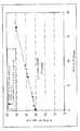
도 8은 슬롯 전류 대 방사상 전류를 도시한 그래프이다.
도 9는 여분의(extra) 씨프 전극 전류 대 추정된 방사상 전류를 도시한 그래프이다.In the drawings, the same element number indicates the same element in each of the drawings.
1 is an exploded perspective view of an electrochemical processor.
FIG. 2 is a perspective view in cross section of the vessel assembly shown in FIG. 1;
3 is an enlarged cross-sectional view of the container assembly.
4 is a schematic perspective view of a cross-section of the upper cup shown in FIG. 3.
5 is a schematic diagram of a control volume near the edge of a wafer in the processor shown in FIG. 1;
6 is a schematic diagram of a control volume near the edge of a wafer in an alternative processor.
7 is an enlarged detailed view of the control volumes shown in FIG. 6.
8 is a graph showing slot current versus radial current.
9 is a graph showing extra shear electrode current versus estimated radial current.
제어 시스템 및 방법은, 프로세서에서의 실시간 측정들을 기초로, 전기도금 프로세서 내에서 하나 또는 둘 이상의 양극들의 전극 셋트 포인트들 및 전류 씨프를 자동적으로 제어할 수 있게 한다. 이는 셋트 포인트 추정치들을 만드는 것에 대한 의존을 줄이고 개선된 전기도금을 제공한다.The control system and method makes it possible to automatically control the electrode set points and current shift of one or more anodes within an electroplating processor based on real-time measurements at the processor. This reduces reliance on making set point estimates and provides improved electroplating.
목적은 웨이퍼 표면에서의 전류를 결정하는 것인데, 이는 이러한 전류가, 전기도금된 필름의 품질 및 균일성에 영향을 미치는 일차적인 인자이기 때문이다. 만약 웨이퍼 표면에서의 전류를 실시간으로 알게 된다면, 전극들에 대한 전류가 요구되는 바에 따라 조정되어서 원하는 결과들을 달성할 수 있다. 반응기 전류들을 적절하게 제어하는데 있어서, 웨이퍼의 단지 하나의 부분(즉, 엣지 부분)에 대해서 전류를 결정하는 것으로 충분할 수 있다.The purpose is to determine the current at the wafer surface, since this current is the primary factor affecting the quality and uniformity of the electroplated film. If the current at the wafer surface is known in real time, the current to the electrodes can be adjusted as required to achieve the desired results. In properly controlling the reactor currents, it may be sufficient to determine the current for only one portion of the wafer (ie, the edge portion).
패터닝된 구리 다마신(damascene) 웨이퍼들을 전기도금하는 것은 초기 전극 셋트 포인트들을 결정하는데 있어서 부가적인 난제들을 제시하는데, 이는 시드 층이 복잡한 피쳐(feature) 패터닝을 커버하기 때문이다. 결과적으로, 초기 시트 저항을 알 수 없다. 피쳐들(예를 들어, 웨이퍼 상의 트렌치들 또는 비아들(vias))이 하단부로부터 위쪽으로 충진됨에 따른 시트 저항의 변화는 정확하게 예측될 수 없다. 계산된 웨이퍼 전류를 통해서 초기 시트 저항을 검출하는 것에 의해서, 본 방법은 이러한 인자들을 극복한다. 이어서, 제어기는 도금 프로세스 중에 변화되는 시트 저항에 대해서 실시간으로 보상한다.Electroplating patterned copper damascene wafers presents additional challenges in determining initial electrode set points, as the seed layer covers complex feature patterning. As a result, the initial sheet resistance is unknown. The change in sheet resistance as features (eg trenches or vias on the wafer) are filled upward from the bottom cannot be predicted accurately. By detecting the initial sheet resistance through the calculated wafer current, the method overcomes these factors. The controller then compensates in real time for the sheet resistance that changes during the plating process.
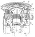
이제 도면들을 구체적으로 설명하면, 도 1-4는 대표적인 도금 프로세서를 도시한다. 그러나, 본 발명의 개념들은, 적어도 하나의 양극 및 전류 씨프 전극을 갖는 사실상 어떤 프로세서에 대해서도 적용할 수 있다. 도 1에 도시된 바와 같이, 전기-화학적 프로세서(20)는 용기 조립체(50) 위에 배치된 헤드(30)를 갖는다. 용기 조립체(50)는 스탠드(38) 또는 다른 구조물에 부착된 데크 플레이트(24) 상에서 지지될 수 있다. 헤드(30)는 리프트(lift)/회전 유닛(34) 상에서 지지될 수 있는데, 이는 헤드를 리프팅시키고 반전(invert)시켜서 웨이퍼(10)를 헤드 내에 로딩 및 언로딩하기 위해서, 그리고 프로세싱을 위해 헤드(30)를 하강시켜 용기 조립체(50)와 맞물리게(engagement) 하기 위해서이다.Referring now to the drawings in detail, FIGS. 1-4 illustrate a representative plating processor. However, the concepts of the present invention are applicable to virtually any processor having at least one anode and a current shear electrode. As shown in FIG. 1, the electro-
이제 도 2-3을 참조하면, 용기 조립체(50)는, 체결부들(60)로 함께 유지되는, 양극 컵(52), 하부 멤브레인(membrane) 지지부(54), 및 상부 멤브레인 지지부(56)를 포함할 수 있다. 양극 컵(52) 내에서, 제 1 또는 내측 양극(70)이 내측 양극 챔버(110)의 하단부 근처에 배치된다. 제 2 또는 외측 양극(72)은 양극액(anolyte) 챔버(110)를 둘러싸는 외측 양극 챔버(112)의 하단부 근처에 배치된다. 상기 양극들은 소모성(comsumable) 양극 재료 즉, 구리 펠릿들(pellets), 볼들 등으로서 제공될 수 있다. 양극 챔버들 내의 전해질은 양극액으로서 지칭된다.Referring now to FIGS. 2-3, the
도 2에 도시된 바와 같이, 내측 양극(70)은 제 1 전기 리드(lead) 또는 커넥터(130)에 전기적으로 연결되고 그리고 외측 양극(72)은 분리된 제 2 전기 리드 또는 커넥터(132)에 전기적으로 연결된다. 전류 씨프 전극(206)은 상부 컵(76)의 상부 단부를 둘러쌀 수 있다.As shown in FIG. 2, the
이제 도 3-4를 참조하면, 상부 컵(76)이 이용되는 경우, 상부 컵(76)은 상부 컵 하우징(58) 내에 수용되거나 상부 컵 하우징(58)에 의해서 둘러싸일 수 있다. 상부 컵 하우징(58)은 상부 컵(76)에 부착되고 상부 컵(76)에 대해서 밀봉된다. 상부 컵(76)은 곡선형 상단부 표면(124) 및 중앙 관통 개구부를 갖고, 중앙 관통 개구부는 중앙 또는 내측 음극 챔버(120)를 형성한다. 이러한 챔버(120)는, 상부 컵(76)의 곡선형 상부 표면(124)에 의해서 정의된 종(bell) 또는 뿔(horn) 형상의 공간 내로 이어지는 확산기(74) 내의 대체로 원통형인 공간에 의해서 정의된다. 일련의 동심적인 환형 슬롯들이 상부 컵(76)의 상단부 곡선형 표면(124)으로부터 하향 연장한다. 상부 컵(76)의 하단부 내에 형성된 외측 음극 챔버(78)가 튜브들의 어레이 또는 다른 통로들을 통해서 슬롯들에 연결된다. 음극 챔버들 내의 전해질은 음극액으로 지칭된다.Referring now to FIGS. 3-4, when the
도 4에 도시된 바와 같이, 하나의 예에서, 8개의 외주방향 슬롯들(90, 92, 94, 96, 98, 100, 102 및 104)이 상부 컵(76)의 곡선형 상부 표면(124)으로부터 하향 연장한다. 슬롯들 내의 볼륨을 충진하는 액체 전해질이 큰 전기 저항을 갖도록, 슬롯들이 좁다. 슬롯들은 전형적으로 1 내지 5 mm, 또는 2-4 mm의 폭을 갖는다. 외주방향 슬롯들은 수직 튜브들(104A, 102A, 100A 및 98A)에 의해서 외측 음극 또는 음극액 챔버(78) 내에 연결된다. 도시된 구체적인 예에서, 18개의 튜브들이 각각의 슬롯에 연결된다. 튜브들은 전기 저항의 일차적인 공급원(source)이다. 슬롯들은 튜브들을 통해서 유동하는 전류를 균일한 선대칭적(axisymmetric) 공급원으로 재분배시키는 것(즉, 팬 아웃(fan out))을 도우며, 그에 따라 웨이퍼가 회전할 때 회전하는 웨이퍼는 균일한 전류(웨이퍼가 홀들 위에서 회전되는 경우의 최대치들과 최소치들 대신)를 확인한다(see). 웨이퍼의 외측 부분에 걸쳐 외측 양극 전류를 적절하게 분배하기 위해 슬롯들이 배치되고 폭이 선택된다.As shown in Figure 4, in one example, eight
도 5를 참조하면, 제어 볼륨(210)은 웨이퍼(10)의 엣지 근처에서 선택된다. 제어 볼륨(210)은 내측 외주방향 경계(212), 외측 외주방향 경계(214), 하부 경계(216), 및 상부 경계(218)를 갖는다. 제어 볼륨(210) 및 그 경계들은 본 시스템 및 방법들을 설명하는데 있어서 유용한 수학적 구성부들(constructs)이다. 제어 볼륨(210) 및 그 경계들은 물리적 요소들이 아니다.Referring to FIG. 5, the
300 mm 직경 웨이퍼들에 대해서 디자인된 프로세서의 경우에, 내측 경계(212)가 웨이퍼 중심으로부터 100 내지 130 mm에 위치될 수 있다. 내측 프로브 또는 참고 전극(202)은 내측 경계(212)의 내향에 위치된다. 외측 프로브 또는 참고 전극(204)은 내측 경계(212)의 외향에 위치되고, 그에 따라 외측 프로브(204)가 제어 볼륨(210) 내에 위치된다. 프로브들(202 및 204)은 와이어들과 같은 실제적인 물리적 요소들이다. 프로브들은 또한 실제적인 물리적 전극 또는 와이어로 연장되는 전해질 충진된 모세관 튜브들로서 제공될 수 있다. 프로브들(202 및 204)은 제어기(200)에 전기적으로 연결될 수 있다. 프로세서 내에서의 전해질 및 전기 전류 유동의 변경(altering)을 감소 또는 방지하기 위해서, 프로브들(202 및 204)은 상부 컵의 상부 표면과 같은 높이(flush)일 수 있다. 내측 프로브 또는 참고 전극(202) 및 외측 프로브 또는 참고 전극(204)은 공통 반경 상에 위치될 수 있고, 용기 조립체(50)의 중심 위치로부터 방사상 외측으로 연장할 수 있다. 또한, 상기 용기 조립체(50)는 반경(R)을 갖고, 그리고 상기 내측 프로브 또는 참고 전극(202)은 상기 중심 위치로부터 적어도 0.65 R에 위치될 수 있다.In the case of a processor designed for 300 mm diameter wafers, the
사용시에, 프로브들은 전압 구배를 측정한다. 오옴의 법칙 V = IR을 이용하여, 내측 경계를 통한 (방사상 외향으로의) 전류 유동을 계산하기 위해 내측 및 외측 프로브들에서 측정된 전압들 사이의 차이가 이용되고, 여기에서 V는 측정된 전압 차이이며, R은 프로브들 사이의 거리(DD)에 걸친 액체 전해질의 저항이고, 그리고 I는 내측 경계를 통해서 유동하는 전류, 또는 방사상 전류 플럭스(flux)(I/방사상-내측(radial-in))이다. DD가 클수록, 주어진 방사상 전류에 대한 측정된 전압이 더 커질 것이다. 전형적으로, 웨이퍼의 직경에 따라서, DD가 10 내지 60 mm 또는 그 초과의 범위일 수 있고, 전형적인 값들은 10 내지 30 mm이다. R은 전해질의 측정된(또는 제조 업자에 의해서 제공된) 저항에 기초하여 그리고 프로브들 사이의 알려진 거리(DD)에 기초하여 알려진다. 도 5에 도시된 예에서, 내측 프로브(202)가 120 mm(웨이퍼 중심 위치로부터 120 mm)의 반경에 있고 외측 프로브(204)가 140 mm에 있으며, 그에 따라 DD는 약 20 mm이다.In use, the probes measure the voltage gradient. Using Ohm's Law V = IR, the difference between the voltages measured at the inner and outer probes is used to calculate the current flow through the inner boundary (radially outward), where V is the measured voltage Is the difference, R is the resistance of the liquid electrolyte over the distance DD between the probes, and I is the current flowing through the inner boundary, or the radial current flux (I/radial-in). )to be. The greater the DD, the greater will be the measured voltage for a given radial current. Typically, depending on the diameter of the wafer, the DD may range from 10 to 60 mm or more, with typical values being from 10 to 30 mm. R is known based on the measured (or provided by the manufacturer) resistance of the electrolyte and based on the known distance (DD) between the probes. In the example shown in FIG. 5, the
외측 경계(214)를 통해서 제어 볼륨(210)의 외부로 유동하는 전류(I/방사상-외측(radial-out))는, 예를 들어 씨프 전극(206)에 연결된 전류계를 통해서 알려진 씨프 전류와 동일하게 셋팅된다. 비록 도 5는 제어 볼륨을 지나서 방사상 외측으로 연장하는 웨이퍼 엣지를 도시하고 있지만, 외측 경계(214)가 웨이퍼 엣지를 지나도록 제어 볼륨이 선택적으로 선택될 수 있고, 그에 따라 I/방사상-외측을 씨프 전류와 같게 하는 것은 적은 오류를 도입하거나 또는 오류가 없다.The current flowing to the outside of the
하부 경계(216)를 통해서 제어 볼륨(210) 내로 유동하는 총 전류(I/수직-내측(vertical-in))는 슬롯들(102 및 104) 내의 전해질을 통해서 유동하는 전류와 동일하다. 상부 컵(76)이 유전체 재료로 제조되고, 그에 따라 상부 컵을 통해서 유동하는 모든 전류는 필연적으로, 상부 컵 내의 전해질 충진된 슬롯들 내에서만 유동하게 된다. 슬롯들을 통한 전류는 외측 양극 전류, 내측 양극 전류 및 씨프 전극 전류의 단편이다. 만약 높은 시트 저항으로 인해서 또는 높은 씨프 전극 전류에 의해서 반응기 내에서 큰 방사상 전압 구배들이 생성된다면, 이러한 전압 구배들은 전류가 내측 슬롯들(90, 92, 94, 96)을 통해 유동하여 내려가고(flow down) 외측 슬롯들(98, 100, 102, 104)을 통해 다시 올라오게(back up) 한다. 슬롯들을 통한 전류 유동은 프로브들에 의해서 측정된 방사상 전류로부터 실제적으로 정확하게 결정될 수 있다. 도 5에서 슬롯들(102 및 104)을 통한 전류 유동은 제어 볼륨의 내측 경계(212)를 통한 방사상 전류 및 외측 양극 전류의 함수이다. 결과적으로, (다이알드-인(dialed-in) 세트들 또는 다이알드-인이 아닌) 반응기 내에서 사용된 임의의 전류들에 대해서, 슬롯들(102 및 104)을 통한 외측 양극 전류의 단편은 라인의 수학식에 의해서 정확하게 예측되는데, 라인의 수학식에서 "x" 값은 참고 전극들로부터 계산된 바와 같은 측정된 전류이다.The total current flowing through the
요약하면, 프로세서 내의 방사상 전류를 연산하기 위해서 2개의 참고 전극들 사이의 단일 전압 차이를 이용하는 것에 의해서, 제어 볼륨의 2개의 측부들(sides)에 걸친 전류가 정확하게 결정될 수 있다(212는 후술되는 수학식 2를 이용하여, 그리고 218은 도 8에 도시된 플롯(plot)을 이용하는 것에 의해서). 2개의 프로브들로부터의 이러한 동일한 단일 방사상 전류는 또한, 웨이퍼 엣지 전류를 그 타겟으로 유도하기 위해 전류들의 새로운 세트를 연산하는데 이용되는 "이득(gain)"을 결정하도록 이용될 수 있다.In summary, by using a single voltage difference between the two reference electrodes to calculate the radial current in the processor, the current across the two sides of the control volume can be accurately determined (212 is the math described below. Using
도 9에 도시된 바와 같이, "이득"이 방사상 전류에 따라서 1로부터 8까지 변화하는 것으로 도시되어 있다. 적절한 이득이 매우 넓게 변화될 수 있기 때문에, 웨이퍼 타겟에 신속하게 도달하고 타겟 상에서 유지되기 위해서, 적절한 값을 이용하는 것이 필요하다. 모델링은, 반응기 내에서 이용되는 전류들이 이미 "다이알-인(dial-in)" 전류들 근처에 있을 때, 적절한 "이득"이 방사상 전류로부터의 선형 관계를 가장 정확하게 따른다는 것을 보여준다. 따라서, 웨이퍼 전류가 타겟에 근접함에 따라, 알고리즘이 더 큰 정확도를 얻는다.As shown in Fig. 9, the "gain" is shown to vary from 1 to 8 depending on the radial current. Since the appropriate gain can be varied very widely, it is necessary to use an appropriate value in order to quickly reach the wafer target and remain on the target. Modeling shows that when the currents used in the reactor are already near the "dial-in" currents, the appropriate "gain" most accurately follows the linear relationship from the radial current. Thus, as the wafer current approaches the target, the algorithm achieves greater accuracy.
타겟(제어 볼륨 내의 웨이퍼 면적에 대한 총 웨이퍼 전류의 %)은 제어 볼륨 내의 웨이퍼 면적의 양과 대체로 동일한 값이다(즉, 편평한 프로파일의 경우에 26.5%). 그러나, 반응기 방사상 전류를 연산하기 위해서 단지 2개의 프로브들만 이용하는 것으로부터의 작은 오류들을 보상하는데 있어서, 타겟 대 방사상 전류에 대한 약간의 조정은 적절하다. 제어 알고리즘에서 알려지지 않은 것들 모두는 단일 전류 플럭스 계산의 함수들로서 표현될 수 있다. 이러한 알려지지 않은 것들은 제어 볼륨 경계들(212 및 218), 이득, 및 % 웨이퍼 전류 타겟이다. 따라서, 프로세스를 제어하기 위해서 챔버 내에서 요구되는 기구(instrumentation)는 비교적 단순할 수 있다.The target (% of total wafer current to wafer area in the control volume) is approximately equal to the amount of wafer area in the control volume (ie, 26.5% for a flat profile). However, in compensating for small errors from using only two probes to calculate the reactor radial current, a slight adjustment to the target to radial current is adequate. All of the unknowns in the control algorithm can be expressed as functions of a single current flux calculation. These unknowns are the
도 5에 도시된 바와 같이, 슬롯 내의 전류 유동을 계산하기 위해서 이용되는 전압 변화를 이용하여 슬롯 내의 전압 변화를 검출하기 위해서, 상부 및 하부 슬롯 프로브들(220 및 222)이 슬롯(102) 내에 뿐만 아니라 슬롯(104) 내에 부가될 수 있다.As shown in Fig. 5, in order to detect the voltage change in the slot using the voltage change used to calculate the current flow in the slot, the upper and lower slot probes 220 and 222 are not only in the
제어 볼륨 내로 유동하는 전류가 제어 볼륨 외부로 유동하는 전류와 반드시 같아야 하기 때문에, I/방사상-내측 더하기 I/수직-내측은 I/방사상-외측 더하기 I/수직-외측과 반드시 같아야 한다. I/수직-외측은 제어 볼륨 내의 웨이퍼 표면에서의 실제 전류로서 셋팅된다. I/수직-외측은 이하의 수학식 1로부터 계산된다.Since the current flowing into the control volume must be equal to the current flowing outside the control volume, I/radial-inner plus I/vertical-inner must be equal to I/radial-outer plus I/vertical-outer. I/Vertical-Outer is set as the actual current at the wafer surface in the control volume. The I/vertical-outer side is calculated from Equation 1 below.

특히 매우 얇은 시드 층들 상에 도금할 때, 시트 저항이 매우 급격하게, 즉 몇 밀리초 내에 10배만큼 변화된다. 웨이퍼 표면에서의 전류, 또는 I/수직-외측은 시트 저항의 함수이다(전극 전류들이 일정할 때). I/수직-외측이 즉각적으로 알려지는 상태에서, 시트 저항의 급격한 변화에서도 개선된 전기도금 결과들을 달성하기 위해서, 제어기(200)는 양극들 및 씨프 전극에 제공되는 전류를 실시간으로 변화시킬 수 있다. 양극(들) 및 씨프 전극 전류들은 2.5 밀리초마다 정도로 신속하게 조정될 수 있다.Particularly when plating on very thin seed layers, the sheet resistance changes very rapidly, ie by a factor of 10 within a few milliseconds. The current at the wafer surface, or I/vertical-outside, is a function of sheet resistance (when the electrode currents are constant). In a state where the I/vertical-outer side is immediately known, in order to achieve improved electroplating results even in a sudden change in sheet resistance, the
도 5의 제어 볼륨(210)이 2-차원들로 도시되어 있다. 프로세서 내의 전류가 3 차원들로 유동하는 동안, 비록 프로브들이 본질적으로, 2 차원적인 구배를 측정하지만, 수학적 모델링은 2개의 프로브들의 이용이 양호한 정확도를 제공한다는 것을 보여준다. 3-차원적인 제어 볼륨에 대해서, 제어 볼륨 내로 방사상으로 유동하는 전류는 이하의 수학식 2로부터 추정될 수 있다.The

여기에서, K는 배쓰 전도도이고 hgap 은 전류 플럭스 측정 위치에서의 웨이퍼의 하향 대면 표면과 상부 컵의 상단부 표면 사이의 수직 갭 또는 공간이다. 전류 플럭스 측정 위치는 내측 프로브(202)와 외측 프로브(204) 사이의 대체로 절반인 위치이다. 대안적으로, 참고 전극들의 180도의 복제(duplicate) 쌍을 이용하여, 경계(212)를 통하는 3 차원적인 전류 유동의 더 양호한 추정을 얻을 수 있다. 또한 링 형태의 참고 전극을 선택적으로 이용하여, 전압 차이 및 플럭스의 더 양호한 3 차원적인 추정을 획득할 수 있다. 방사상 외측으로 유동하는 전류를 단일 전압 차이가 정확하게 연산할 수 있는 위치에 프로브들이 효과적으로 배치된다.Where K is the bath conductivity and hgap is the vertical gap or space between the downward facing surface of the wafer and the top surface of the upper cup at the current flux measurement position. The current flux measurement position is a position that is generally halfway between the
도 2 및 5를 참조하면, 제어기(200)가 프로브들(202 및 204)에 전기적으로 연결되고 프로브들로부터의 입력들을 이용하여 전압 구배를 계산한다. 이어서, 제어기는 전술한 바와 같이 I/수직-외측을 계산한다. 이어서, 계산된 I/수직-외측은 저장된 타겟 값에 대해서 비교될 수 있다. 이들 간의 차이는 오류 신호를 제공한다. 제어기는 오류 신호를 이용하여, 양극(들) 및 씨프 전극에 의해서 공급되는 전류들을 조정한다. 만약 I/수직-외측이 너무 높다면, 제어기는 I/수직-외측을 감소시키기 위해서 씨프 전류를 증가시킬 수 있다.2 and 5, a
특히 둘 또는 셋 이상의 양극들을 갖는 프로세서들에서 제어를 단순화하기 위해서, 외측 양극에 대한 전류가, 예를 들어 헤드(30)의 특정 높이를 선택하는 것에 의해 모든 시트 저항들에 대해서 일정하도록, 프로세서가 셋업될 수 있다. 이어서, I/수직-외측에 기초하여, 단지 씨프 전류 비율만 제어하면 된다. 씨프 전류 비율은 내측 양극 전류에 대한 씨프 전류의 비율이다. 씨프 전류 비율만을 조정하는 것은 둘 또는 셋 이상의 양극들을 갖는 프로세서들에서 제어를 단순화시킨다.In order to simplify control, especially in processors with two or more anodes, the processor must be made so that the current to the outer anode is constant for all sheet resistances, for example by choosing a specific height of the
하나의 형태에서 방법은 이하와 같이 실시될 수 있다:In one form the method can be implemented as follows:
a. 임의의 전류 세트 및 웨이퍼 시트 저항에 대해서, 프로브 위치들에서 전기 전위(potential)를 탐색한다.a. For any current set and wafer sheet resistance, search for the electrical potential at the probe locations.
b. 프로브들 사이의 측정된 전압 구배를 이용하여 방사상 전류 플럭스를 계산한다.b. The radial current flux is calculated using the measured voltage gradient between the probes.
c. 웨이퍼 엣지로 진행하는 전류를 결정하기 위해서 전술한 바와 같은 제어 볼륨 분석을 이용한다.c. Control volume analysis as described above is used to determine the current going to the wafer edge.
d. 웨이퍼 엣지 전류를 타겟 엣지 전류에 대해서 비교한다.d. The wafer edge current is compared against the target edge current.
e. 웨이퍼 엣지 전류를 타겟으로 유도하기 위해 전류들의 새로운 세트를 계산한다.e. A new set of currents is calculated to drive the wafer edge current to the target.
도 6 및 7은 범용 전기도금 프로세서에 적용된 바와 같은 전술한 방법을 도시하고, 범용 전기도금 프로세서는 제어 볼륨의 하부 경계에서의 전류 밀도가 실질적으로 균일하도록, 단일 양극(300), 단일 씨프 전극(206), 및 매우 큰 전기 저항을 갖는 확산기(302)를 갖는다.6 and 7 show the above-described method as applied to a general-purpose electroplating processor, in which the general-purpose electroplating processor has a
두꺼운 또는 얇은 프로파일들의 엣지를 야기하기 위해서, 엣지 전류에 대한 타겟 값이 조정될 수 있다. 프로파일을 편평하게 하여 시스템 오류들을 밝히기 위해서 타겟의 경험적인(empirical) 조정이 이용될 수 있다. 예를 들어, 26.75% 대신에, 27.5% 타겟 전류가 더 편평한 프로파일을 야기할 수 있다. 절연 웨이퍼(또는 베어(bare) 실리콘 웨이퍼)를 이용하여 내측 양극과 씨프 전극 사이에서 특정 전류를 유동시키는 것에 의해서, 방사상 전류 플럭스의 프로브 계산의 교정(calibration)이 달성될 수 있다. 이어서, 모든 전류가 방사상이 되어, 요구되는 인자들(배쓰 전도도, 웨이퍼-대-벽 갭, 프로브 방사상 거리)의 체크 또는 셋팅을 허용한다. 여러 가지 제품 웨이퍼들에 대해서 동적인 전류 제어(DCC) 레시피들(recipes)(즉, 시간에 걸친, 각각의 전극으로부터의 즉각적인(instantaneous) 전류)를 "기록(write)"하기 위해서, 자동적인, 인-시츄(in-situ) 제어가 이용될 수 있다. 기록된 DCC 레시피는 생산에서 이용될 수 있고, 그에 따라 동일한 레시피가 각각의 웨이퍼에서 항상 이용된다. 수정 "감도(sensitivity)" 도함수(derivative)(즉, 이득)는, 다음의 반복(iteration)을 위한 "감도"를 예측하는데 이용되는 이전의 반복에 응답하여 "작동 중에(on-the-fly)" 계산될 수 있다.In order to cause the edge of thick or thin profiles, the target value for the edge current can be adjusted. An empirical adjustment of the target can be used to flatten the profile to reveal system errors. For example, instead of 26.75%, a 27.5% target current can result in a flatter profile. By using an insulating wafer (or a bare silicon wafer) to flow a specific current between the inner anode and the sipe electrode, a calibration of the probe calculation of the radial current flux can be achieved. All currents are then radial, allowing the checking or setting of the required factors (bath conductivity, wafer-to-wall gap, probe radial distance). Automatic, to "write" dynamic current control (DCC) recipes (ie, instantaneous current from each electrode over time) for various product wafers In-situ control can be used. The recorded DCC recipe can be used in production, so the same recipe is always used on each wafer. The modified "sensitivity" derivative (ie, gain) is "on-the-fly" in response to the previous iteration used to predict the "sensitivity" for the next iteration. "Can be calculated.
여기에서 사용된 바와 같은 '웨이퍼'라는 용어는 마이크로전자 디바이스, 마이크로-기계적 디바이스, 및/또는 마이크로-광학적 디바이스를 갖는 다른 기판들 및 공작물들을 포함한다. 여기에서 설명된 방법들은 하나 또는 둘 이상의 양극들 및 단일 씨프 전극을 갖는 프로세서들에서 이용될 수 있다. 여기에서 사용된 바와 같은 '연결된' 또는 '전기적으로 연결된'이라는 용어는 무선 및 유선 연결들 모두를 포함한다.The term'wafer' as used herein includes microelectronic devices, micro-mechanical devices, and/or other substrates and workpieces having micro-optical devices. The methods described herein may be used in processors with one or more anodes and a single sipe electrode. The term'connected' or'electrically connected' as used herein includes both wireless and wired connections.
Claims (12)
Translated fromKorean전해질을 홀딩(holding)하기 위한 용기;
상기 용기 내의 적어도 하나의 양극, 전류 씨프, 및 필드 성형(field shaping) 유닛;
제 1 및 제 2의 이격된 참고 전극들로서, 제 1 참고 전극은 상기 용기의 중심 위치와 제 2 참고 전극 사이에 위치되는, 제 1 및 제 2 참고 전극들; 및
상기 적어도 하나의 양극, 상기 전류 씨프, 및 상기 제 1 및 제 2 참고 전극들에 전기적으로 연결되는 제어기를 포함하고,
상기 제어기는:
웨이퍼의 엣지 근처에서 전해질 내의 전압 구배를 결정하는 단계;
상기 전압 구배를 이용하여 상기 웨이퍼의 엣지 근처의 전해질의 볼륨 내로의 방사상 전기 전류 유동을 결정하는 단계;
상기 볼륨으로부터 씨프 전극으로의 방사상 전기 전류 유동을 결정하는 단계;
상기 볼륨 내로의 수직 전기 전류 유동을 결정하는 단계;
상기 씨프 전극으로의 방사상 전류 유동을 상기 볼륨 내로의 방사상 전류 유동과 상기 볼륨 내로의 수직 전기 전류 유동의 합으로부터 차감함으로써, 상기 웨이퍼 표면으로의 전기 전류 유동을 계산하는 단계;
상기 웨이퍼 표면으로의 전류 유동을 타겟 값으로부터 차감함으로써 오류 값을 결정하는 단계; 및
상기 양극 및 상기 씨프 전극 중 적어도 하나로의 전기 전류 유동을 제어하기 위해서 상기 오류 값을 이용하는 단계
에 의해 상기 전기도금 처리기를 제어하는,
전기도금 처리기.As an electroplating processor,
A container for holding an electrolyte;
At least one anode, current shear, and field shaping unit in the vessel;
First and second spaced apart reference electrodes, the first reference electrode being positioned between a center position of the container and a second reference electrode; And
A controller electrically connected to the at least one anode, the current sief, and the first and second reference electrodes,
The controller:
Determining a voltage gradient in the electrolyte near the edge of the wafer;
Determining a radial electric current flow into a volume of electrolyte near an edge of the wafer using the voltage gradient;
Determining a radial electric current flow from the volume to a sipe electrode;
Determining a vertical electric current flow into the volume;
Calculating an electric current flow to the wafer surface by subtracting the radial current flow to the sipe electrode from the sum of the radial current flow into the volume and the normal electric current flow into the volume;
Determining an error value by subtracting the current flow to the wafer surface from a target value; And
Using the error value to control the flow of electric current to at least one of the anode and the sipe electrode
Controlling the electroplating processor by,
Electroplating processor.
상기 제 1 및 제 2 참고 전극들은 공통 반경 상에 위치되고 상기 중심 위치로부터 방사상 외측으로 연장하는, 전기도금 처리기.The method of claim 1,
The first and second reference electrodes are located on a common radius and extend radially outward from the central position.
상기 제 1 및 제 2 전극들은 상기 필드 성형 유닛 내에 또는 상기 필드 성형 유닛 상에 있는, 전기도금 처리기.The method of claim 1,
The first and second electrodes are in or on the field shaping unit.
상기 필드 성형 유닛은 곡선형의 상단부 표면을 갖는 상부 컵 및 복수의 외주방향 슬롯들을 포함하고, 그리고 적어도 하나의 상기 외주방향 슬롯은 상기 제 1 및 제 2 참고 전극들 사이에 있는, 전기도금 처리기.The method of claim 1,
The field forming unit comprises an upper cup having a curved top surface and a plurality of circumferential slots, and at least one circumferential slot is between the first and second reference electrodes.
씨프 전극은 상기 용기의 상부 엣지 주위로 연장하는 링을 포함하고, 그리고 상기 제 2 참고 전극은 상기 씨프 전극과 상기 제 1 참고 전극 사이에 있는, 전기도금 처리기.The method of claim 1,
Wherein the sipe electrode includes a ring extending around an upper edge of the vessel, and the second reference electrode is between the sipe electrode and the first reference electrode.
상기 용기는 반경(R)을 갖고, 그리고 상기 제 1 전극은 상기 중심 위치로부터 적어도 0.65 R에 위치되는, 전기도금 처리기.The method of claim 2,
The vessel has a radius R, and the first electrode is located at least 0.65 R from the central position.
상기 용기와 맞물릴 수 있는(engageable) 헤드를 더 포함하고, 상기 헤드는 웨이퍼를 상기 제 2 참고 전극 위로 5-30 mm에서 홀딩하기 위한 웨이퍼 홀딩 위치를 갖는, 전기도금 처리기.The method of claim 1,
The electroplating processor further comprising a head engageable with the vessel, the head having a wafer holding position for holding a wafer at 5-30 mm above the second reference electrode.
상기 제 2 참고 전극은 상기 제 1 참고 전극보다 더 높은 수직 위치에 있는, 전기도금 처리기.The method of claim 1,
Wherein the second reference electrode is in a higher vertical position than the first reference electrode.
하나 또는 둘 이상의 외주방향 슬롯들 내에 보충적인 참고 전극들을 더 포함하는, 전기도금 처리기.The method of claim 4,
The electroplating processor further comprising supplemental reference electrodes in one or more circumferential slots.
웨이퍼의 엣지 근처에서 전해질 내의 전압 구배를 결정하는 단계;
상기 전압 구배를 이용하여 상기 웨이퍼의 엣지 근처의 전해질의 볼륨 내로의 방사상 전기 전류 유동을 결정하는 단계;
상기 볼륨으로부터 씨프 전극으로의 방사상 전기 전류 유동을 결정하는 단계;
상기 볼륨 내로의 수직 전기 전류 유동을 결정하는 단계;
상기 씨프 전극으로의 방사상 전류 유동을 상기 볼륨 내로의 방사상 전류 유동과 상기 볼륨 내로의 수직 전기 전류 유동의 합으로부터 차감함으로써, 상기 웨이퍼 표면으로의 전기 전류 유동을 계산하는 단계;
상기 웨이퍼 표면으로의 전류 유동을 타겟 값으로부터 차감함으로써 오류 값을 결정하는 단계; 및
상기 양극 및 상기 씨프 전극 중 적어도 하나로의 전기 전류 유동을 제어하기 위해서 상기 오류 값을 이용하는 단계를 포함하는, 전기도금 처리기를 제어하는 방법.A method of controlling an electroplating processor having at least one anode and a sipe electrode,
Determining a voltage gradient in the electrolyte near the edge of the wafer;
Determining a radial electric current flow into a volume of electrolyte near an edge of the wafer using the voltage gradient;
Determining a radial electric current flow from the volume to a sipe electrode;
Determining a vertical electric current flow into the volume;
Calculating an electric current flow to the wafer surface by subtracting the radial current flow to the sipe electrode from the sum of the radial current flow into the volume and the normal electric current flow into the volume;
Determining an error value by subtracting the current flow to the wafer surface from a target value; And
Using the error value to control the flow of electric current to at least one of the anode and the sipe electrode.
상기 웨이퍼 표면으로의 전기 전류 유동에 기초하여 시트 저항을 결정하는 단계를 더 포함하는, 전기도금 처리기를 제어하는 방법.The method of claim 10,
Determining a sheet resistance based on the flow of electrical current to the wafer surface.
상기 처리기는 내측 양극 및 외측 양극을 갖고 상기 웨이퍼는 헤드 내에 있으며, 상기 외측 양극으로부터의 전류는 상기 전해질 표면에 대해 상기 헤드의 특정 높이를 선택하는 것에 의해서 모든 시트 저항들에 대해서 일정하게 유지되고, 그리고 상기 씨프 전류를 제어하는 단계를 더 포함하는, 전기도금 처리기를 제어하는 방법.The method of claim 10,
The processor has an inner anode and an outer anode and the wafer is in the head, and the current from the outer anode is kept constant for all sheet resistances by choosing a specific height of the head relative to the electrolyte surface, And controlling the sipe current.
Applications Claiming Priority (2)
| Application Number | Priority Date | Filing Date | Title |
|---|---|---|---|
| US13/920,709 | 2013-06-18 | ||
| US13/920,709US20140367264A1 (en) | 2013-06-18 | 2013-06-18 | Automatic in-situ control of an electro-plating processor |
Publications (2)
| Publication Number | Publication Date |
|---|---|
| KR20140147044A KR20140147044A (en) | 2014-12-29 |
| KR102156786B1true KR102156786B1 (en) | 2020-09-16 |
Family
ID=52018290
Family Applications (1)
| Application Number | Title | Priority Date | Filing Date |
|---|---|---|---|
| KR1020140073535AActiveKR102156786B1 (en) | 2013-06-18 | 2014-06-17 | Automatic insitu control of an electro-plating processor |
Country Status (4)
| Country | Link |
|---|---|
| US (1) | US20140367264A1 (en) |
| KR (1) | KR102156786B1 (en) |
| CN (1) | CN104233423A (en) |
| TW (1) | TW201504480A (en) |
Families Citing this family (5)
| Publication number | Priority date | Publication date | Assignee | Title |
|---|---|---|---|---|
| US9758897B2 (en) | 2015-01-27 | 2017-09-12 | Applied Materials, Inc. | Electroplating apparatus with notch adapted contact ring seal and thief electrode |
| US9765443B2 (en)* | 2015-09-02 | 2017-09-19 | Applied Materials, Inc. | Electroplating processor with current thief electrode |
| US10023969B2 (en)* | 2016-05-24 | 2018-07-17 | Applied Materials, Inc. | Plating power supply with headroom control and ethercat interface |
| US10494731B2 (en)* | 2017-12-11 | 2019-12-03 | Applied Materials, Inc. | Electroplating dynamic edge control |
| SG11202106509UA (en)* | 2018-12-28 | 2021-07-29 | Acm Research Shanghai Inc | Plating apparatus and plating method |
Citations (1)
| Publication number | Priority date | Publication date | Assignee | Title |
|---|---|---|---|---|
| US20040007467A1 (en)* | 2002-05-29 | 2004-01-15 | Mchugh Paul R. | Method and apparatus for controlling vessel characteristics, including shape and thieving current for processing microfeature workpieces |
Family Cites Families (6)
| Publication number | Priority date | Publication date | Assignee | Title |
|---|---|---|---|---|
| US6916412B2 (en)* | 1999-04-13 | 2005-07-12 | Semitool, Inc. | Adaptable electrochemical processing chamber |
| US6231743B1 (en)* | 2000-01-03 | 2001-05-15 | Motorola, Inc. | Method for forming a semiconductor device |
| US8308931B2 (en)* | 2006-08-16 | 2012-11-13 | Novellus Systems, Inc. | Method and apparatus for electroplating |
| DE10232612B4 (en)* | 2002-07-12 | 2006-05-18 | Atotech Deutschland Gmbh | Apparatus and method for monitoring an electrolytic process |
| US7645364B2 (en)* | 2004-06-30 | 2010-01-12 | Lam Research Corporation | Apparatus and method for plating semiconductor wafers |
| US7837851B2 (en)* | 2005-05-25 | 2010-11-23 | Applied Materials, Inc. | In-situ profile measurement in an electroplating process |
- 2013
- 2013-06-18USUS13/920,709patent/US20140367264A1/ennot_activeAbandoned
- 2014
- 2014-05-27TWTW103118468Apatent/TW201504480A/enunknown
- 2014-06-17KRKR1020140073535Apatent/KR102156786B1/enactiveActive
- 2014-06-18CNCN201410273606.2Apatent/CN104233423A/enactivePending
Patent Citations (1)
| Publication number | Priority date | Publication date | Assignee | Title |
|---|---|---|---|---|
| US20040007467A1 (en)* | 2002-05-29 | 2004-01-15 | Mchugh Paul R. | Method and apparatus for controlling vessel characteristics, including shape and thieving current for processing microfeature workpieces |
Also Published As
| Publication number | Publication date |
|---|---|
| KR20140147044A (en) | 2014-12-29 |
| US20140367264A1 (en) | 2014-12-18 |
| TW201504480A (en) | 2015-02-01 |
| CN104233423A (en) | 2014-12-24 |
Similar Documents
| Publication | Publication Date | Title |
|---|---|---|
| US7837851B2 (en) | In-situ profile measurement in an electroplating process | |
| KR102156786B1 (en) | Automatic insitu control of an electro-plating processor | |
| JP6861610B2 (en) | Plating analysis method, plating analysis system, and computer program for plating analysis | |
| US6444101B1 (en) | Conductive biasing member for metal layering | |
| US8496789B2 (en) | Electrochemical processor | |
| KR102784541B1 (en) | Plating apparatus | |
| KR20110020226A (en) | Method for measuring thickness of conductive layer and device using same | |
| JP2001192898A (en) | Method for forming semi-conductor device | |
| KR20160122076A (en) | Monitoring electrolytes during electroplating | |
| US12308251B2 (en) | Electrochemical additive manufacturing system having conductive seed layer | |
| US6761812B2 (en) | Apparatus and method for electrochemical metal deposition | |
| JP4989541B2 (en) | Plating method, semiconductor device manufacturing method, and plating processing system | |
| CN1860259A (en) | A method and a system for automatically controlling a current distribution of a multi-anode arrangement during the plating of a metal on a substrate surface | |
| US7710130B2 (en) | Volume resistivity measurement apparatus for dielectric layer of electrostatic chuck and measurement method using the apparatus | |
| KR20060090822A (en) | Method and system for automatically controlling current distribution in multi-anode configuration during plating of metal on substrate surface | |
| US9469911B2 (en) | Electroplating apparatus with membrane tube shield | |
| US20040099534A1 (en) | Method and apparatus for electroplating a semiconductor wafer | |
| US8147670B2 (en) | Profile control on ring anode plating chambers for multi-step recipes | |
| TW202204699A (en) | Leveling compound control | |
| JP2022532943A (en) | Electrochemical deposition system including optical probe | |
| US20240167188A1 (en) | Detection of contact formation between a substrate and contact pins in an electoplating system | |
| WO2017070924A1 (en) | Method for electrochemical polish in constant voltage mode | |
| US20060289299A1 (en) | Multi-channel current probe | |
| KR20110077914A (en) | Electroplating Device and Method for Semiconductor |
Legal Events
| Date | Code | Title | Description |
|---|---|---|---|
| PA0109 | Patent application | Patent event code:PA01091R01D Comment text:Patent Application Patent event date:20140617 | |
| PG1501 | Laying open of application | ||
| PA0201 | Request for examination | Patent event code:PA02012R01D Patent event date:20190104 Comment text:Request for Examination of Application Patent event code:PA02011R01I Patent event date:20140617 Comment text:Patent Application | |
| E902 | Notification of reason for refusal | ||
| PE0902 | Notice of grounds for rejection | Comment text:Notification of reason for refusal Patent event date:20200428 Patent event code:PE09021S01D | |
| E701 | Decision to grant or registration of patent right | ||
| PE0701 | Decision of registration | Patent event code:PE07011S01D Comment text:Decision to Grant Registration Patent event date:20200901 | |
| GRNT | Written decision to grant | ||
| PR0701 | Registration of establishment | Comment text:Registration of Establishment Patent event date:20200910 Patent event code:PR07011E01D | |
| PR1002 | Payment of registration fee | Payment date:20200910 End annual number:3 Start annual number:1 | |
| PG1601 | Publication of registration | ||
| PR1001 | Payment of annual fee | Payment date:20230828 Start annual number:4 End annual number:4 | |
| PR1001 | Payment of annual fee | Payment date:20240826 Start annual number:5 End annual number:5 |