KR102154501B1 - Display device and method for driving thereof - Google Patents
Display device and method for driving thereofDownload PDFInfo
- Publication number
- KR102154501B1 KR102154501B1KR1020140045314AKR20140045314AKR102154501B1KR 102154501 B1KR102154501 B1KR 102154501B1KR 1020140045314 AKR1020140045314 AKR 1020140045314AKR 20140045314 AKR20140045314 AKR 20140045314AKR 102154501 B1KR102154501 B1KR 102154501B1
- Authority
- KR
- South Korea
- Prior art keywords
- transistor
- voltage
- electrode
- switch
- data line
- Prior art date
- Legal status (The legal status is an assumption and is not a legal conclusion. Google has not performed a legal analysis and makes no representation as to the accuracy of the status listed.)
- Expired - Fee Related
Links
Images


Classifications
- G—PHYSICS
- G09—EDUCATION; CRYPTOGRAPHY; DISPLAY; ADVERTISING; SEALS
- G09G—ARRANGEMENTS OR CIRCUITS FOR CONTROL OF INDICATING DEVICES USING STATIC MEANS TO PRESENT VARIABLE INFORMATION
- G09G3/00—Control arrangements or circuits, of interest only in connection with visual indicators other than cathode-ray tubes
- G09G3/20—Control arrangements or circuits, of interest only in connection with visual indicators other than cathode-ray tubes for presentation of an assembly of a number of characters, e.g. a page, by composing the assembly by combination of individual elements arranged in a matrix no fixed position being assigned to or needed to be assigned to the individual characters or partial characters
- G09G3/22—Control arrangements or circuits, of interest only in connection with visual indicators other than cathode-ray tubes for presentation of an assembly of a number of characters, e.g. a page, by composing the assembly by combination of individual elements arranged in a matrix no fixed position being assigned to or needed to be assigned to the individual characters or partial characters using controlled light sources
- G09G3/30—Control arrangements or circuits, of interest only in connection with visual indicators other than cathode-ray tubes for presentation of an assembly of a number of characters, e.g. a page, by composing the assembly by combination of individual elements arranged in a matrix no fixed position being assigned to or needed to be assigned to the individual characters or partial characters using controlled light sources using electroluminescent panels
- G09G3/32—Control arrangements or circuits, of interest only in connection with visual indicators other than cathode-ray tubes for presentation of an assembly of a number of characters, e.g. a page, by composing the assembly by combination of individual elements arranged in a matrix no fixed position being assigned to or needed to be assigned to the individual characters or partial characters using controlled light sources using electroluminescent panels semiconductive, e.g. using light-emitting diodes [LED]
- G09G3/3208—Control arrangements or circuits, of interest only in connection with visual indicators other than cathode-ray tubes for presentation of an assembly of a number of characters, e.g. a page, by composing the assembly by combination of individual elements arranged in a matrix no fixed position being assigned to or needed to be assigned to the individual characters or partial characters using controlled light sources using electroluminescent panels semiconductive, e.g. using light-emitting diodes [LED] organic, e.g. using organic light-emitting diodes [OLED]
- G—PHYSICS
- G09—EDUCATION; CRYPTOGRAPHY; DISPLAY; ADVERTISING; SEALS
- G09G—ARRANGEMENTS OR CIRCUITS FOR CONTROL OF INDICATING DEVICES USING STATIC MEANS TO PRESENT VARIABLE INFORMATION
- G09G5/00—Control arrangements or circuits for visual indicators common to cathode-ray tube indicators and other visual indicators
- G09G5/18—Timing circuits for raster scan displays
- G—PHYSICS
- G09—EDUCATION; CRYPTOGRAPHY; DISPLAY; ADVERTISING; SEALS
- G09G—ARRANGEMENTS OR CIRCUITS FOR CONTROL OF INDICATING DEVICES USING STATIC MEANS TO PRESENT VARIABLE INFORMATION
- G09G2230/00—Details of flat display driving waveforms
- G—PHYSICS
- G09—EDUCATION; CRYPTOGRAPHY; DISPLAY; ADVERTISING; SEALS
- G09G—ARRANGEMENTS OR CIRCUITS FOR CONTROL OF INDICATING DEVICES USING STATIC MEANS TO PRESENT VARIABLE INFORMATION
- G09G2300/00—Aspects of the constitution of display devices
- G09G2300/04—Structural and physical details of display devices
- G09G2300/0421—Structural details of the set of electrodes
- G09G2300/0426—Layout of electrodes and connections
- G—PHYSICS
- G09—EDUCATION; CRYPTOGRAPHY; DISPLAY; ADVERTISING; SEALS
- G09G—ARRANGEMENTS OR CIRCUITS FOR CONTROL OF INDICATING DEVICES USING STATIC MEANS TO PRESENT VARIABLE INFORMATION
- G09G2300/00—Aspects of the constitution of display devices
- G09G2300/08—Active matrix structure, i.e. with use of active elements, inclusive of non-linear two terminal elements, in the pixels together with light emitting or modulating elements
- G09G2300/0809—Several active elements per pixel in active matrix panels
- G09G2300/0842—Several active elements per pixel in active matrix panels forming a memory circuit, e.g. a dynamic memory with one capacitor
- G—PHYSICS
- G09—EDUCATION; CRYPTOGRAPHY; DISPLAY; ADVERTISING; SEALS
- G09G—ARRANGEMENTS OR CIRCUITS FOR CONTROL OF INDICATING DEVICES USING STATIC MEANS TO PRESENT VARIABLE INFORMATION
- G09G2310/00—Command of the display device
- G09G2310/06—Details of flat display driving waveforms
- G09G2310/061—Details of flat display driving waveforms for resetting or blanking
- G09G2310/063—Waveforms for resetting the whole screen at once
- G—PHYSICS
- G09—EDUCATION; CRYPTOGRAPHY; DISPLAY; ADVERTISING; SEALS
- G09G—ARRANGEMENTS OR CIRCUITS FOR CONTROL OF INDICATING DEVICES USING STATIC MEANS TO PRESENT VARIABLE INFORMATION
- G09G2320/00—Control of display operating conditions
- G09G2320/06—Adjustment of display parameters
- G09G2320/0693—Calibration of display systems
- G—PHYSICS
- G09—EDUCATION; CRYPTOGRAPHY; DISPLAY; ADVERTISING; SEALS
- G09G—ARRANGEMENTS OR CIRCUITS FOR CONTROL OF INDICATING DEVICES USING STATIC MEANS TO PRESENT VARIABLE INFORMATION
- G09G2360/00—Aspects of the architecture of display systems
- G09G2360/14—Detecting light within display terminals, e.g. using a single or a plurality of photosensors
- G09G2360/145—Detecting light within display terminals, e.g. using a single or a plurality of photosensors the light originating from the display screen
- G09G2360/147—Detecting light within display terminals, e.g. using a single or a plurality of photosensors the light originating from the display screen the originated light output being determined for each pixel
- G—PHYSICS
- G09—EDUCATION; CRYPTOGRAPHY; DISPLAY; ADVERTISING; SEALS
- G09G—ARRANGEMENTS OR CIRCUITS FOR CONTROL OF INDICATING DEVICES USING STATIC MEANS TO PRESENT VARIABLE INFORMATION
- G09G3/00—Control arrangements or circuits, of interest only in connection with visual indicators other than cathode-ray tubes
- G09G3/20—Control arrangements or circuits, of interest only in connection with visual indicators other than cathode-ray tubes for presentation of an assembly of a number of characters, e.g. a page, by composing the assembly by combination of individual elements arranged in a matrix no fixed position being assigned to or needed to be assigned to the individual characters or partial characters
- G09G3/22—Control arrangements or circuits, of interest only in connection with visual indicators other than cathode-ray tubes for presentation of an assembly of a number of characters, e.g. a page, by composing the assembly by combination of individual elements arranged in a matrix no fixed position being assigned to or needed to be assigned to the individual characters or partial characters using controlled light sources
- G09G3/30—Control arrangements or circuits, of interest only in connection with visual indicators other than cathode-ray tubes for presentation of an assembly of a number of characters, e.g. a page, by composing the assembly by combination of individual elements arranged in a matrix no fixed position being assigned to or needed to be assigned to the individual characters or partial characters using controlled light sources using electroluminescent panels
- G09G3/32—Control arrangements or circuits, of interest only in connection with visual indicators other than cathode-ray tubes for presentation of an assembly of a number of characters, e.g. a page, by composing the assembly by combination of individual elements arranged in a matrix no fixed position being assigned to or needed to be assigned to the individual characters or partial characters using controlled light sources using electroluminescent panels semiconductive, e.g. using light-emitting diodes [LED]
- G09G3/3208—Control arrangements or circuits, of interest only in connection with visual indicators other than cathode-ray tubes for presentation of an assembly of a number of characters, e.g. a page, by composing the assembly by combination of individual elements arranged in a matrix no fixed position being assigned to or needed to be assigned to the individual characters or partial characters using controlled light sources using electroluminescent panels semiconductive, e.g. using light-emitting diodes [LED] organic, e.g. using organic light-emitting diodes [OLED]
- G09G3/3225—Control arrangements or circuits, of interest only in connection with visual indicators other than cathode-ray tubes for presentation of an assembly of a number of characters, e.g. a page, by composing the assembly by combination of individual elements arranged in a matrix no fixed position being assigned to or needed to be assigned to the individual characters or partial characters using controlled light sources using electroluminescent panels semiconductive, e.g. using light-emitting diodes [LED] organic, e.g. using organic light-emitting diodes [OLED] using an active matrix
- G09G3/3233—Control arrangements or circuits, of interest only in connection with visual indicators other than cathode-ray tubes for presentation of an assembly of a number of characters, e.g. a page, by composing the assembly by combination of individual elements arranged in a matrix no fixed position being assigned to or needed to be assigned to the individual characters or partial characters using controlled light sources using electroluminescent panels semiconductive, e.g. using light-emitting diodes [LED] organic, e.g. using organic light-emitting diodes [OLED] using an active matrix with pixel circuitry controlling the current through the light-emitting element
Landscapes
- Engineering & Computer Science (AREA)
- Physics & Mathematics (AREA)
- Computer Hardware Design (AREA)
- General Physics & Mathematics (AREA)
- Theoretical Computer Science (AREA)
- Multimedia (AREA)
- Control Of El Displays (AREA)
- Control Of Indicators Other Than Cathode Ray Tubes (AREA)
- Electroluminescent Light Sources (AREA)
Abstract
Translated fromKoreanDescription
Translated fromKorean본 발명은 표시장치 및 그 구동 방법에 관한 것으로, 보다 상세하게는 화소의 장시간 구동에 따른 열화 현상을 개선하기 위한 표시장치 및 그 구동 방법에 관한 것이다.The present invention relates to a display device and a driving method thereof, and more particularly, to a display device and a driving method thereof for improving a deterioration phenomenon caused by driving a pixel for a long time.
음극선관(Cathode Ray Tube)의 단점인 무게와 부피를 줄일 수 있는 각종 평판 표시 장치들이 개발되고 있다. 평판 표시 장치로는 액정 표시 장치(Liquid Crystal Display: LCD), 전계방출 표시 장치(Field Emission Display: FED), 플라즈마 표시패널(Plasma Display Panel: PDP) 및 유기 발광 표시 장치(Organic Light Emitting Display: OLED) 등이 있다.Various flat panel display devices that can reduce the weight and volume, which are disadvantages of a cathode ray tube, are being developed. Flat panel displays include Liquid Crystal Display (LCD), Field Emission Display (FED), Plasma Display Panel (PDP), and Organic Light Emitting Display (OLED). ), etc.
평판 표시 장치 중 유기 발광 표시 장치는 전자와 정공의 재결합에 의하여 빛을 발생하는 유기 발광 다이오드를 이용하여 영상을 표시하는 것으로서, 빠른 응답속도를 가짐과 동시에 낮은 소비전력으로 구동되고 발광효율, 휘도 및 시야각이 뛰어난 장점이 있어 주목 받고 있다.Among flat panel displays, an organic light emitting diode displays an image using an organic light emitting diode that generates light through recombination of electrons and holes. It has a fast response speed and is driven with low power consumption. It is attracting attention because of its excellent viewing angle.
통상적으로, 유기 발광 표시 장치(OLED)는 유기 발광 다이오드를 구동하는 방식에 따라 패시브 매트릭스형 유기 발광 표시장치(PMOLED)와 액티브 매트릭스형 유기 발광 표시장치(AMOLED)로 분류된다.In general, the organic light emitting display device OLED is classified into a passive matrix type organic light emitting display device (PMOLED) and an active matrix type organic light emitting display device (AMOLED) according to a method of driving an organic light emitting diode.
이 중 해상도, 콘트라스트, 동작속도의 관점에서 단위 화소마다 선택하여 점등하는 액티브 매트릭스형 OLED(AMOLED)가 주류가 되고 있다. 액티브 매트릭스형 유기 발광 표시장치의 한 화소는 유기 발광 다이오드, 유기 발광 다이오드에 공급되는 전류량을 제어하는 제1트랜지스터, 및 제1트랜지스터로 유기 발광 다이오드의 발광량을 제어하는 데이터 신호를 전달하는 스위칭 트랜지스터를 포함한다.Among them, active matrix type OLEDs (AMOLEDs), which are selected and turned on for each unit pixel from the viewpoint of resolution, contrast, and operation speed, are becoming mainstream. One pixel of the active matrix type organic light emitting diode display includes an organic light emitting diode, a first transistor that controls the amount of current supplied to the organic light emitting diode, and a switching transistor that transmits a data signal that controls the amount of light emitted from the organic light emitting diode to the first transistor. Include.
한편, 유기 발광 표시장치의 발광 시간이 길어지는 경우, 각 화소별 광 출력량이 서로 다르게 나타나고, 휘도가 불균일해져 화질이 저하되는 현상이 발생한다.On the other hand, when the emission time of the organic light emitting display device is prolonged, the amount of light output for each pixel is different from each other, and the luminance becomes uneven, resulting in a phenomenon in which image quality is deteriorated.
따라서, 화소의 열화 정보를 센싱하여 열화된 화소에 보정된 데이터 신호를 전달함으로써 휘도를 균일하게 출력하는 화소 보상 회로가 필요하다.Accordingly, there is a need for a pixel compensation circuit that senses deterioration information of a pixel and transmits a corrected data signal to the deteriorated pixel to uniformly output luminance.
본 발명의 일 실시예는 표시장치 및 그 구동방법을 제공하고자 한다. 이를 위하여 본 발명의 일 실시예는 화소 회로에 광 센싱부를 배치하여 화소의 정밀한 계조 표현이 이루어질 수 있는 고품질, 고화질의 표시 장치와 그 구동 방법을 제안하고자 한다.An embodiment of the present invention is to provide a display device and a driving method thereof. To this end, an exemplary embodiment of the present invention is to propose a high-quality, high-definition display device and a driving method thereof capable of displaying a precise gray scale of a pixel by arranging a light sensing unit in a pixel circuit.
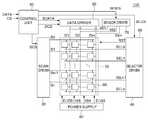
본 발명의 일 실시예는 복수의 주사선으로 복수의 주사신호를 전달하는 주사 구동부; 복수의 데이터선으로 복수의 데이터 신호를 전달하는 데이터 구동부; 복수의 선택 신호선으로 복수의 선택 신호를 전달하는 선택 구동부; 상기 복수의 데이터선으로 복수의 출력 신호를 전달받는 센서 구동부; 및 상기 주사선, 상기 데이터선 및 상기 선택 신호선과 각각 연결된 복수의 화소;를 포함하고, 상기 복수의 화소 각각은, 제1전원과 제2전원 사이에 연결된 유기발광다이오드; 상기 유기발광다이오드에 상기 데이터 신호에 따른 구동 전류를 전달하는 제1트랜지스터; 상기 주사 신호에 대응하여 상기 제1 트랜지스터의 게이트 전극과 상기 데이터선을 연결하는 제2트랜지스터; 상기 제1전원과 상기 제1트랜지스터의 게이트 전극 사이에 연결된 제1 커패시터; 제3 전원과 연결된 수광 소자; 상기 수광 소자 및 제4 전원 사이에 연결된 제2 커패시터; 게이트 전극이 상기 선택 신호선에 연결되고, 상기 데이터선 및 상기 제2 커패시터의 제1 전극 사이에 연결된 제3 트랜지스터; 및 게이트 전극이 상기 제2 커패시터의 제1 전극에 연결되고, 제4 전원과 상기제3 트랜지스터 사이에 연결된 제4 트랜지스터;를 포함하는 표시장치를 제공한다.An embodiment of the present invention provides a scan driver for transmitting a plurality of scan signals to a plurality of scan lines; A data driver transferring a plurality of data signals to a plurality of data lines; A selection driver for transmitting a plurality of selection signals to a plurality of selection signal lines; A sensor driver receiving a plurality of output signals through the plurality of data lines; And a plurality of pixels respectively connected to the scan line, the data line, and the selection signal line, wherein each of the plurality of pixels comprises: an organic light emitting diode connected between a first power source and a second power source; A first transistor transferring a driving current according to the data signal to the organic light emitting diode; A second transistor connecting the gate electrode of the first transistor and the data line in response to the scan signal; A first capacitor connected between the first power source and the gate electrode of the first transistor; A light receiving element connected to a third power source; A second capacitor connected between the light receiving element and a fourth power source; A third transistor having a gate electrode connected to the selection signal line and connected between the data line and a first electrode of the second capacitor; And a fourth transistor having a gate electrode connected to the first electrode of the second capacitor and connected between a fourth power source and the third transistor.
본 발명의 일 실시예에 따르면, 상기 수광 소자는, 캐소드 전극이 상기 제3 전원과 연결되고, 애노드 전극이 상기 제2 커패시터의 제1 전극에 연결되는 PIN 다이오드, PN 다이오드 및 포토 커플러 중 적어도 하나를 포함할 수 있다.According to an embodiment of the present invention, the light receiving element includes at least one of a PIN diode, a PN diode, and a photo coupler in which a cathode electrode is connected to the third power source, and an anode electrode is connected to the first electrode of the second capacitor. It may include.
본 발명의 일 실시예에 따르면, 상기 제3 트랜지스터는, 제1 전극이 상기 데이터선에 연결되고, 제2 전극이 상기 제4 트랜지스터의 제1 전극과 연결될 수 있다.According to an embodiment of the present invention, in the third transistor, a first electrode may be connected to the data line, and a second electrode may be connected to the first electrode of the fourth transistor.
본 발명의 일 실시예에 따르면, 상기 제4 트랜지스터는, 제1 전극이 상기 제3 트랜지스터의 제2 전극과 연결되고, 제2 전극이 상기 제4 전원에 연결될 수 있다.According to an embodiment of the present invention, in the fourth transistor, a first electrode may be connected to a second electrode of the third transistor, and a second electrode may be connected to the fourth power source.
본 발명의 일 실시예에 따르면, 상기 데이터 구동부와 상기 데이터선 사이에 연결된 제1 스위치를 더 포함할 수 있다.According to an embodiment of the present invention, a first switch connected between the data driver and the data line may be further included.
본 발명의 일 실시예에 따르면, 상기 센서 구동부와 상기 데이터선 사이에 연결된 제2 스위치를 더 포함할 수 있다.According to an embodiment of the present invention, a second switch connected between the sensor driver and the data line may be further included.
본 발명의 일 실시예에 따르면, 제5 전원; 및 상기 제5 전원과 상기 제2 스위치 사이에 연결된 제3 스위치를 더 포함할 수 있다.According to an embodiment of the present invention, a fifth power source; And a third switch connected between the fifth power source and the second switch.
본 발명의 일 실시예에 따르면, 상기 센서 구동부는 상기 데이터선과 연결되는 ADC(Analog Digital Converter)를 더 포함할 수 있다.According to an embodiment of the present invention, the sensor driver may further include an ADC (Analog Digital Converter) connected to the data line.
본 발명의 일 실시예는 복수의 주사선으로 복수의 주사신호를 전달하는 주사 구동부; 복수의 데이터선으로 복수의 데이터 신호를 전달하는 데이터 구동부; 복수의 선택 신호선으로 복수의 선택 신호를 전달하는 선택 구동부; 상기 데이터선으로 복수의 출력 신호를 전달받는 센서 구동부; 상기 주사선, 상기 데이터선 및 상기 선택 신호선과 각각 연결된 복수의 화소; 상기 데이터 구동부와 상기 데이터선 사이에 연결된 제1 스위치; 상기 센서 구동부와 상기 데이터선 사이에 연결된 제2 스위치; 및 제5 전원과 상기 제2 스위치 사이에 연결된 제3 스위치를 포함하고, 상기 화소는 제1전원과 제2전원 사이에 연결된 유기발광다이오드, 상기 유기발광다이오드에 상기 데이터 신호에 따른 구동 전류를 전달하는 제1트랜지스터, 상기 주사 신호에 대응하여 상기 제1 트랜지스터의 게이트 전극과 상기 데이터선을 연결하는 제2트랜지스터, 상기 제1전원과 상기 제1트랜지스터의 게이트 전극 사이에 연결된 제1 커패시터, 제3 전원과 연결된 수광 소자, 상기 수광 소자 및 제4 전원 사이에 연결된 제2 커패시터, 게이트 전극이 상기 선택 신호선에 연결되며 상기 데이터선 및 상기 제2 커패시터의 제1 전극 사이에 연결된 제3 트랜지스터, 및 게이트 전극이 상기 제2 커패시터의 제1 전극에 연결되며 제4 전원과 상기 제3 트랜지스터 사이에 연결된 제4 트랜지스터를 포함하는 표시장치의 구동 방법에 있어서, 상기 제3 트랜지스터의 제1 전극 전압이 상기 데이터선을 통하여 상기 센서 구동부에 저장되는 초기전압 저장 단계; 상기 데이터 신호에 따른 구동전류로 상기 유기발광다이오드가 발광하고, 상기 수광소자에 입사되는 광의 세기에 따라 발생되는 광 누설 전류에 의하여 상기 제2 캐패시터의 전압이 변동되는 광 감지 단계; 및 광 감지에 의해 변동된 상기 제2 캐패시터 전압이 반영된 상기 제3 트랜지스터의 제1 전극 전압이 상기 데이터선을 통하여 상기 센서 구동부에 저장되는 센싱 전압 저장 단계;를 포함하는 표시장치의 구동방법을 제공한다.An embodiment of the present invention provides a scan driver for transmitting a plurality of scan signals to a plurality of scan lines; A data driver transferring a plurality of data signals to a plurality of data lines; A selection driver for transmitting a plurality of selection signals to a plurality of selection signal lines; A sensor driver receiving a plurality of output signals through the data line; A plurality of pixels respectively connected to the scan line, the data line, and the selection signal line; A first switch connected between the data driver and the data line; A second switch connected between the sensor driver and the data line; And a third switch connected between a fifth power source and the second switch, wherein the pixel includes an organic light emitting diode connected between the first power source and the second power source, and transfers a driving current according to the data signal to the organic light emitting diode. A first transistor, a second transistor connecting the gate electrode of the first transistor and the data line in response to the scan signal, a first capacitor connected between the first power source and the gate electrode of the first transistor, and a third A light receiving element connected to a power source, a second capacitor connected between the light receiving element and a fourth power source, a third transistor having a gate electrode connected to the selection signal line and connected between the data line and the first electrode of the second capacitor, and a gate A method of driving a display device including a fourth transistor having an electrode connected to a first electrode of the second capacitor and connected between a fourth power source and the third transistor, wherein the first electrode voltage of the third transistor is Storing an initial voltage stored in the sensor driving unit through a line; A photo-sensing step in which the organic light-emitting diode emits light with a driving current according to the data signal, and a voltage of the second capacitor is changed by a light leakage current generated according to the intensity of light incident on the light receiving element; And storing a sensing voltage in which the first electrode voltage of the third transistor, in which the second capacitor voltage varied by light sensing is reflected, is stored in the sensor driver through the data line. do.
본 발명의 일 실시예에 따르면, 상기 센서 구동부가 상기 초기 전압과 상기 센싱 전압을 비교하여 제2 캐패시터 전압의 변화량을 계산하는 단계; 상기 제2 캐패시터 전압의 변화량을 이용하여 각 화소의 열화 정보를 판단하는 단계; 및 열화된 화소에 보정된 데이터 신호를 전송하는 단계;를 더 포함할 수 있다.According to an embodiment of the present invention, the sensor driver compares the initial voltage and the sensing voltage to calculate a change amount of the second capacitor voltage; Determining deterioration information of each pixel using a change amount of the second capacitor voltage; And transmitting the corrected data signal to the deteriorated pixel.
본 발명의 일 실시예에 따르면, 상기 초기 전압 저장 단계는, 상기 제1 스위치가 턴 오프 되고, 상기 제2 스위치가 턴 온 되고, 상기 제3 스위치가 턴 온 되고, 상기 수광소자의 캐소드 전극에 제3 전원 전압이 인가되고, 상기 제3 트랜지스터가 선택신호에 따라 스위칭 동작하여 상기 제4 트랜지스터의 제1 전극과 상기 데이터선을 연결하고, 상기 제2 트랜지스터는 턴 오프 되고, 상기 데이터선을 통하여 상기 제3 트랜지스터의 제1 전극에 상기 제5전원의 전압이 인가되는 제1 단계; 및 상기 제3 스위치가 턴 오프 되고, 상기 제3 트랜지스터의 제1 전극 전압이 상기 데이터선을 통하여 상기 센서 구동부에 저장되는 제2 단계;를 포함할 수 있다.According to an embodiment of the present invention, in the initial voltage storage step, the first switch is turned off, the second switch is turned on, the third switch is turned on, and the cathode electrode of the light receiving device is When a third power voltage is applied, the third transistor performs a switching operation according to a selection signal to connect the first electrode of the fourth transistor and the data line, and the second transistor is turned off, through the data line. A first step of applying the voltage of the fifth power source to the first electrode of the third transistor; And a second step of turning off the third switch and storing a first electrode voltage of the third transistor in the sensor driver through the data line.
본 발명의 일 실시예에 따르면, 상기 제1 단계는, 상기 제1 스위치가 턴 오프 되어 상기 데이터 구동부와 상기 데이터선을 단선시키고, 상기 제2 스위치가 턴 온 되어 상기 센서 구동부와 상기 데이터선을 연결하고, 상기 제3 스위치가 턴 온 되어 상기 제5전원의 전압과 상기 데이터선을 연결하고, 상기 수광소자의 캐소드 전극에 상기 제3 전원의 전압이 인가되어 이에 대응되는 전압이 상기 제2 커패시터에 저장될 수 있다.According to an embodiment of the present invention, in the first step, the first switch is turned off to disconnect the data driver and the data line, and the second switch is turned on to connect the sensor driver and the data line. And the third switch is turned on to connect the voltage of the fifth power source to the data line, and the voltage of the third power source is applied to the cathode electrode of the light-receiving device, and the voltage corresponding thereto is the second capacitor Can be stored in.
본 발명의 일 실시예에 따르면, 상기 광 감지 단계는, 상기 제1 스위치가 턴 온 되고, 상기 제2 스위치가 턴 오프 되고, 상기 제3 스위치가 턴 오프 되고, 제2 트랜지스터가 데이터 신호에 따라 스위칭 동작하여 상기 제1 트랜지스터의 게이트 전극과 상기 데이터선을 연결하고, 상기 제3 트랜지스터는 턴 오프 되고, 상기 수광소자에 입사되는 광의 세기에 따라 발생되는 광 누설 전류에 의하여 상기 제2 캐패시터의 전압이 변동될 수 있다.According to an embodiment of the present invention, in the photo-sensing step, the first switch is turned on, the second switch is turned off, the third switch is turned off, and the second transistor is turned off according to a data signal. A switching operation is performed to connect the gate electrode of the first transistor to the data line, and the third transistor is turned off, and the voltage of the second capacitor is caused by a light leakage current generated according to the intensity of light incident on the light receiving device. This can fluctuate.
본 발명의 일 실시예에 따르면, 상기 센싱 전압 저장 단계는, 상기 제1 스위치가 턴 오프 되고, 상기 제2 스위치가 턴 온 되고, 상기 제3 스위치가 턴 온 되고, 제3 트랜지스터가 선택신호에 따라 스위칭 동작하여 상기 제4 트랜지스터의 제1 전극과 상기 데이터선을 연결하고, 제2 트랜지스터는 턴 오프 되고, 상기 데이터선을 통하여 상기 제3 트랜지스터의 제1 전극에 제5전원 전압이 인가되는 제4 단계; 및 상기 제3 스위치가 턴 오프 되고, 상기 제3 단계에서 광 감지에 의해 변동된 제2 캐패시터 전압이 반영된 상기 제4 트랜지스터의 제1 전극 전압이 상기 데이터선을 통하여 상기 센서 구동부에 저장되는 제5 단계;를 포함할 수 있다.According to an embodiment of the present invention, in the storing of the sensing voltage, the first switch is turned off, the second switch is turned on, the third switch is turned on, and the third transistor is applied to the selection signal. A switching operation is performed to connect the first electrode of the fourth transistor to the data line, the second transistor is turned off, and a fifth power supply voltage is applied to the first electrode of the third transistor through the data line. Step 4; And a fifth electrode voltage of the fourth transistor, in which the third switch is turned off, and the second capacitor voltage changed by light sensing in the third step is reflected, is stored in the sensor driver through the data line. Step; may include.
본 발명의 일 실시예에 따르면, 상기 제4 단계는, 상기 제1 스위치가 턴 오프 되어 상기 데이터 구동부와 상기 데이터선을 단락시키고, 상기 제2 스위치가 턴 온 되어 상기 센서 구동부와 상기 데이터선을 연결하고, 상기 제3 스위치가 턴 온 되어 상기 제5전원 전압과 상기 데이터선을 연결할 수 있다.According to an embodiment of the present invention, in the fourth step, the first switch is turned off to short-circuit the data driver and the data line, and the second switch is turned on to connect the sensor driver and the data line. Then, the third switch is turned on to connect the fifth power voltage and the data line.
본 발명에 따른 표시장치는 열화된 화소를 센싱하고 열화된 화소에 보정된 데이터 전압을 인가함으로써 화소의 열화 현상을 개선 하여 고품질 및 고화질을 구현할 수 있다.The display device according to the present invention senses the deteriorated pixel and applies a corrected data voltage to the deteriorated pixel, thereby improving the deterioration of the pixel, thereby realizing high quality and high quality.
도 1은 본 발명의 일 실시예에 따른 표시장치를 개략적으로 도시한 블록도이다.
도 2는 도1에 도시된 표시장치의 화소 회로 구조를 나타내는 회로도이다.
도 3은 도 1에 도시된 센서 구동부 및 데이터 구동부와 데이터선 사이에 연결된 스위치를 개략적으로 나타낸 블록도이다.
도4는 도2에 도시된 화소의 하나의 프레임동안 구동 동작을 나타내는 타이밍도이다.
도 5a 내지 도 5c는 도4에 도시된 타이밍도에 의해 구동되는 도2의 화소의 구동방법을 순차적으로 도시한 회로도 및 타이밍도이다.1 is a block diagram schematically illustrating a display device according to an exemplary embodiment of the present invention.
FIG. 2 is a circuit diagram illustrating a pixel circuit structure of the display device shown in FIG. 1.
3 is a block diagram schematically illustrating a sensor driver illustrated in FIG. 1 and a switch connected between the data driver and the data line.
FIG. 4 is a timing diagram illustrating a driving operation during one frame of the pixel shown in FIG. 2.
5A to 5C are circuit diagrams and timing diagrams sequentially showing a method of driving the pixel of FIG. 2 driven by the timing diagram shown in FIG. 4.
본 발명의 이점 및 특징, 그리고 그것들을 달성하는 방법은 첨부되는 도면과 함께 상세하게 후술되어 있는 실시예들을 참조하면 명확해질 것이다. 그러나 본 발명은 이하에서 개시되는 실시예들에 한정되는 것이 아니라 서로 다른 다양한 형태로 구현될 것이며, 단지 본 실시예들은 본 발명의 개시가 완전하도록 하며, 본 발명이 속하는 기술분야에서 통상의 지식을 가진 자에게 발명의 범주를 완전하게 알려주기 위해 제공되는 것이며, 본 발명은 청구항의 범주에 의해 정의될 뿐이다. 따라서, 몇몇 실시예에서, 잘 알려진 공정 단계들, 잘 알려진 소자 구조 및 잘 알려진 기술들은 본 발명이 모호하게 해석되는 것을 피하기 위하여 구체적으로 설명되지 않는다. 명세서 전체에 걸쳐 동일 참조 부호는 동일 구성 요소를 지칭한다.Advantages and features of the present invention, and a method of achieving them will become apparent with reference to the embodiments described below in detail together with the accompanying drawings. However, the present invention is not limited to the embodiments disclosed below, but will be implemented in a variety of different forms, and only these embodiments make the disclosure of the present invention complete, and common knowledge in the technical field to which the present invention pertains. It is provided to completely inform the scope of the invention to those who have it, and the invention is only defined by the scope of the claims. Accordingly, in some embodiments, well-known process steps, well-known device structures, and well-known techniques have not been described in detail in order to avoid obscuring interpretation of the present invention. The same reference numerals refer to the same components throughout the specification.
본 명세서에서 사용된 용어는 실시예들을 설명하기 위한 것이며 본 발명을 제한하고자 하는 것은 아니다. 어떤 부분이 다른 부분과 "연결"되어 있다고 할 때, 이는 "직접적으로 연결"되어 있는 경우뿐 아니라, 그 중간에 다른 소자를 사이에 두고 "전기적으로 연결"되어 있는 경우도 포함한다. 본 명세서에서, 단수형은 문구에서 특별히 언급하지 않는 한 복수형도 포함한다. 명세서에서 사용되는 "포함한다(comprises)" 및/또는 "포함하는(comprising)"은 언급된 구성요소, 단계, 동작 및/또는 소자는 하나 이상의 다른 구성요소, 단계, 동작 및/또는 소자의 존재 또는 추가를 배제하지 않는다.The terms used in the present specification are for describing exemplary embodiments and are not intended to limit the present invention. When a part is said to be "connected" with another part, this includes not only "directly connected" but also "electrically connected" with another element in between. In this specification, the singular form also includes the plural form unless specifically stated in the phrase. As used in the specification, "comprises" and/or "comprising" refers to the presence of one or more other components, steps, actions and/or elements, and/or elements, steps, actions and/or elements mentioned. Or does not exclude additions.
다른 정의가 없다면, 본 명세서에서 사용되는 모든 용어(기술 및 과학적 용어를 포함)는 본 발명이 속하는 기술분야에서 통상의 지식을 가진 자에게 공통적으로 이해될 수 있는 의미로 사용될 수 있을 것이다. 또 일반적으로 사용되는 사전에 정의되어 있는 용어들은 명백하게 특별히 정의되어 있지 않은 한 이상적으로 또는 과도하게 해석되지 않는다.Unless otherwise defined, all terms (including technical and scientific terms) used in the present specification may be used as meanings that can be commonly understood by those of ordinary skill in the art to which the present invention belongs. In addition, terms defined in a commonly used dictionary are not interpreted ideally or excessively unless explicitly defined specifically.
이하, 도 1 내지 도 5c를 참조하여, 본 발명의 일 실시예에 따른 표시장치 및 구동방법에 대하여 상세히 설명한다.Hereinafter, a display device and a driving method according to an exemplary embodiment will be described in detail with reference to FIGS. 1 to 5C.
도 1은 본 발명의 일 실시예에 따른 표시장치를 개략적으로 도시한 블록도이다.1 is a block diagram schematically illustrating a display device according to an exemplary embodiment of the present invention.
도 1을 참조하면, 본 발명의 실시 예에 의한 표시 장치(100)는 복수의 화소를 포함하는 표시 패널(10), 화소 회로에 주사 신호를 인가하는 주사 구동부(20), 데이터선을 통하여 화소 회로에 데이터 신호를 공급하는 데이터 구동부(30), 화소 회로의 센싱부에 선택 신호를 공급하는 선택 구동부(40), 제어부(50), 표시장치에 외부 전압을 공급하는 전원 공급부(60) 및 화소 회로의 열화 정보를 센싱하는 센서 구동부(70)를 포함한다.Referring to FIG. 1, a
복수의 화소 각각은 표시 패널(10)에 전달되는 복수의 주사선(S0 내지 Sn) 중 하나의 주사선에 연결되어 있다.Each of the plurality of pixels is connected to one of the plurality of scan lines S0 to Sn transmitted to the
또한 복수의 화소 각각은 표시 패널(10)에 전달되는 복수의 데이터선(D1 내지 Dm) 중 하나의 데이터선, 표시 패널(10)에 전달되는 복수의 선택 신호선(SEL0 내지 SELn) 중 하나의 선택 신호선에 연결되어 있다.In addition, each of the plurality of pixels selects one data line among a plurality of data lines D1 to Dm transmitted to the
표시 패널(10)은 디지털 구동 방식으로 구동될 수 있다. 디지털 구동 방식은 데이터 신호에 따라 각 화소의 발광 시간을 조절하여 계조를 표시하는 구동 방식이다. 화소는 인가되는 제1 전원(ELVDD) 및 제2 전원(ELVSS)에 의해 발광하고, 데이터 신호에 의해 발광 시간이 조절되어 계조가 표시된다. 이때, 동일한 계조를 표시하더라도, 화소에 인가되는 제1 전원(ELVDD) 및 제2 전원(ELVSS)의 전압값에 따라 휘도가 달라질 수 있다.The
한편, 표시 패널(10)은 제1 전원(ELVDD) 및 제2 전원(ELVSS)을 제공받아 동작하는 유기발광 패널일 수 있다. 유기발광 패널에 포함된 화소들은 각각 유기발광 다이오드를 포함한다. 제1 전원(ELVDD) 및 제2 전원(ELVSS)이 인가되어 유기발광 다이오드를 통해 전류가 흐르면서 광이 방출된다. 그러나, 이에 제한되는 것은 아니다. 표시 패널(10)은 자체 발광 소자를 포함하는 다양한 종류의 패널 중 하나일 수 있다.Meanwhile, the
제어부(50)는 주사 구동부(20), 데이터 구동부(30), 선택 구동부(40), 전원공급부(60) 및 센서 구동부(70)를 제어한다. 제어부(50)는 외부로부터 수신된 영상 데이터(DATA) 및 제어신호(CS)에 기초하여 주사 구동부(20), 데이터 구동부(30), 선택 구동부(40), 전원공급부(60) 및 센서 구동부(70)를 제어하기 위한 신호들을 생성하고, 주사 구동부(20), 데이터 구동부(30), 선택 구동부(40), 전원공급부(60) 및 센서 구동부(70)에 상기 생성된 신호를 제공한다. 예컨대, 제어신호(CS)는 수직동기신호(Vsync), 수평동기신호(Hsync), 클럭신호(CLK) 및 데이터 인에이블신호(DE) 등의 타이밍 신호이고, 영상 데이터(DATA)는 화소(80)에서 출력되는 광의 계조를 나타내는 디지털 신호일 수 있다.The
주사 구동부(20)는 제어부(50)로부터 주사제어신호(SCS)를 제공받아 주사 신호를 생성한다. 그리고, 주사 구동부(20)는 생성된 주사 신호를 복수의 주사선(S0 내지 Sn)을 통해 각 화소에 주사 신호를 생성하여 전달한다. 상기 주사 신호에 따라 한 행씩의 화소들이 순차적으로 선택되어 데이터 신호가 제공될 수 있다.The
데이터 구동부(30)는 제어부(50)로부터 데이터 제어신호(DCS)를 제공받아 복수의 데이터선(D1 내지 Dm)을 통해 각 화소에 데이터 신호를 전달한다.The
선택 구동부(40)는 제어부(50)로부터 선택 제어신호(SELCS)를 제공받아 복수의 선택 신호선(SEL0 내지 SELn)을 통해 각 화소에 선택 신호를 전달한다. 또한, 선택 구동부(40)는 각 화소에 제3 전원(RST)을 공급할 수 있다. 제3 전원(RST)은 가변 전압일 수 있다. 예를 들면, 제3 전원(RST)은 로우 레벨의 전압과 하이 레벨의 전압으로 변경될 수 있다.The
전원 공급부(60)는 제1 전원(ELVDD), 제2 전원(ELVSS), 제4 전원(VSS) 및 제5 전원(VSH)을 생성하여 표시 패널(10)로 제공한다. 제1 전원(ELVDD) 및 제2 전원(ELVSS)은 표시 패널(110)의 복수의 화소에 공통적으로 인가되어, 화소를 발광시킨다. 제1 전원(ELVDD) 및 제2 전원(ELVSS)의 전압값에 따라 발광 시 화소에 흐르는 전류값이 결정될 수 있다. 화소가 발광할 때, 화소에 흐르는 전류, 즉 구동 전류의 전류값이 달라지면, 동일한 계조를 표시하더라도, 휘도가 달라질 수 있다. 제1 전원(ELVDD)은 구동 전원일 수 있고, 제2 전원(ELVSS)은 접지 전원일 수 있다.The
센서 구동부(70)는 제어부(50)로부터 센서 제어신호(SENCS)를 제공받아 각 화소의 열화 정보를 센싱한다. 각 화소의 열화 정보는 화소 회로의 센싱부에서 전달된 전압들을 비교하여 얻어진다. 센서 구동부(70)는 각 화소의 열화 정보에 따라 각 화소에 인가되는 데이터 신호를 변경시키는 제어신호를 데이터 구동부(30)에 전달한다. 물론, 센서 구동부(70)는 데이터 신호를 변경시키는 제어신호를 제어부(50)에 전달하고, 제어부(50)가 데이터 구동부(30)에 변경된 데이터 제어 신호를 전달할 수 있다.The
표시 패널(10)는 복수의 주사선(S0 내지 Sn), 복수의 데이터선(D1 내지 Dm), 및 복수의 발광 제어선(EM1 내지 EMn)의 교차부에 위치되는 복수의 화소를 포함한다.The
도 1의 실시 예에서 n번째 화소 라인에 포함된 복수의 화소 중 하나인 화소(80)는 해당 n번째 화소 라인에 대응하는 주사선(Sn)과 n번째 화소 라인에 대응하는 선택 신호선(SELn)에 각각 연결된다.In the exemplary embodiment of FIG. 1, the
화소(80)는 주사선(Sn)을 통해 주사 신호를 전달받고, 선택 신호선(SELn)을 통해 선택 신호를 전달받는다. The
상기 복수의 화소는 전원 공급부(60)로부터 제1 전원(ELVDD), 제2 전원(ELVSS), 제4 전원(VSS), 제5 전원(VSH) 등 외부 전압을 공급받는다. 제1 전원(ELVDD)은 제2 전원(ELVSS)보다 높은 전압 레벨을 가진다. 제4 전원(VSS)은 접지 전압일 수 있다. 제5 전원(VSH)은 제3 트랜지스터의 제1 전극을 초기화하는 초기화전압일 수 있다. The plurality of pixels receive external voltages such as first power ELVDD, second power ELVSS, fourth power VSS, and fifth power VSH from the
표시 패널(10)는 대략 행렬 형태로 배열된 복수의 화소를 포함한다. 특별히 제한되지 않으나, 복수의 주사선(S0내지 Sn)은 상기 화소들의 배열 형태에서 대략 행 방향으로 뻗으며 서로가 거의 평행하고, 복수의 데이터선(D1 내지 Dm)은 대략 열 방향으로 뻗으며 서로가 거의 평행하다.The
복수의 화소 각각은 복수의 데이터선(D1 내지 Dm)을 통해 전달된 대응하는 데이터 신호에 따라 유기발광다이오드로 공급되는 구동 전류에 의해 소정 휘도의 빛을 발광한다. Each of the plurality of pixels emit light of a predetermined luminance by a driving current supplied to the organic light emitting diode according to a corresponding data signal transmitted through the plurality of data lines D1 to Dm.
하기에서는 도2를 참조하여 본 발명의 일 실시예에 따른 표시 장치(100)의 화소(80) 회로 구조에 대해 설명한다.Hereinafter, a circuit structure of the
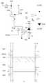
도 2는 도1에 도시된 표시장치의 화소 회로 구조를 나타내는 회로도이다.FIG. 2 is a circuit diagram illustrating a pixel circuit structure of the display device shown in FIG. 1.
도 2를 참조하면, 화소(80)는 도 1의 표시 장치(100) 중 표시 패널(10)에 포함된 복수의 화소 중 n번째 주사선(Sn)과 n번째 선택 신호선(SELn)에 각각 연결된다. 또한 화소(80)는 m번째 데이터선(Dm)에 연결된다.Referring to FIG. 2, a
각각의 트랜지스터는 게이트 전극, 제1전극 및 제2전극을 포함한다. 제1전극은 소스 전극일 수 있고, 제2전극은 드레인 전극일 수 있다. 각각의 트랜지스터는 P 타입으로 구현한 경우를 설명한다. 물론, 각각의 트랜지스터는 N타입으로 구성될 수 있다.Each transistor includes a gate electrode, a first electrode and a second electrode. The first electrode may be a source electrode, and the second electrode may be a drain electrode. A case where each transistor is implemented as a P type will be described. Of course, each transistor may be of an N type.
도 2에 도시된 화소(80)는 화소부(81) 및 센싱부(82)를 포함한다.The
화소부(81)는 유기 발광 다이오드(organic light emitting diode, OLED), 제1트랜지스터(T1), 제2트랜지스터(T2), 제1 커패시터(C1)를 포함한다.The
센싱부(82)는 제3트랜지스터(T3), 제4트랜지스터(T4), 수광소자(PD) 및 제2커패시터(C2)를 포함한다.The
도 2에 도시된 제 1 트랜지스터(T1) 내지 제 4 트랜지스트(T4)는 P 형 트랜지스터을 나타내고 있으나 N 형 트랜지스터일 수도 있다.The first to fourth transistors T1 to T4 shown in FIG. 2 represent a P-type transistor, but may be an N-type transistor.
제1트랜지스터(T1)는 제3 노드(N3)에 연결된 게이트 전극, 유기 발광 다이오드(OLED)에 연결된 제2 전극, 및 제1 전원(ELVDD)에 연결된 제1 전극을 포함한다.The first transistor T1 includes a gate electrode connected to the third node N3, a second electrode connected to the organic light emitting diode OLED, and a first electrode connected to the first power ELVDD.
제1트랜지스터(T1)는 m 번째 데이터선(Dm)과 제2트랜지스터(T2)를 통해 제1트랜지스터(T1)에 인가되는 데이터 신호(D[m])에 따른 데이터 전압의 구동 전류를 생성하여 제2 전극을 통해 유기 발광 다이오드(OLED)에 전달한다. 구동 전류는 제1트랜지스터(T1)의 제1 전극과 게이트 전극 간의 전압 차에 대응하는 전류로서, 게이트 전극에 인가되는 데이터 신호에 따른 데이터 전압에 대응하여 구동 전류(I1)가 달라진다.The first transistor T1 generates a driving current of the data voltage according to the data signal D[m] applied to the first transistor T1 through the m-th data line Dm and the second transistor T2. It is transmitted to the organic light emitting diode (OLED) through the second electrode. The driving current is a current corresponding to a voltage difference between the first electrode of the first transistor T1 and the gate electrode, and the driving current I1 varies in response to a data voltage according to a data signal applied to the gate electrode.
제2트랜지스터(T2)는 n 번째 주사선(Sn)에 연결된 게이트 전극, m 번째 데이터선(Dm)에 연결된 제1 전극, 및 제1 커패시터(C1)의 전극과 제1 트랜지스터(T1)의 게이트 전극이 공통으로 연결된 제3 노드(N3)에 연결된 제2 전극을 포함한다.The second transistor T2 is a gate electrode connected to an n-th scan line Sn, a first electrode connected to an m-th data line Dm, an electrode of the first capacitor C1 and a gate electrode of the first transistor T1. And a second electrode connected to the third node N3 connected in common.
제2트랜지스터(T2)는 n 번째 주사선(Sn)을 통해 전달되는 대응하는 주사 신호(S[n])에 응답하여 화소(80)의 구동을 활성화시킨다. 즉, 제2트랜지스터(T2)는 주사 신호(S[n])에 응답하여 m 번째 데이터선(Dm)을 통해 전달되는 데이터 신호(D[m])에 따른 데이터 전압을 제3 노드(N3)에 전달한다.The second transistor T2 activates the driving of the
제1 커패시터(C1)는 제3 노드(N3)에 연결된 일전극과 제1 전원(ELVDD)의 공급선에 연결된 타전극을 포함한다. 제1 커패시터(C1)는 상술한 바와 같이 제1트랜지스터(T1)의 게이트 전극과 제1 전원(ELVDD)의 공급선 사이에 연결되어 있으므로, 제1트랜지스터(T1)의 게이트 전극에 인가되는 전압을 유지할 수 있다.The first capacitor C1 includes one electrode connected to the third node N3 and the other electrode connected to the supply line of the first power ELVDD. As described above, the first capacitor C1 is connected between the gate electrode of the first transistor T1 and the supply line of the first power ELVDD, so that the voltage applied to the gate electrode of the first transistor T1 is maintained. I can.
제3트랜지스터(T3)는 n 번째 선택 신호선(SELn)에 연결된 게이트 전극, m 번째 데이터선(Dm)에 연결된 제1 전극, 및 제4 트랜지스터(T4)의 제1 전극과 연결된 제2 전극을 포함한다.The third transistor T3 includes a gate electrode connected to the n-th selection signal line SELn, a first electrode connected to the m-th data line Dm, and a second electrode connected to the first electrode of the fourth transistor T4. do.
제3트랜지스터(T3)는 n 번째 선택 신호선(SELn)을 통해 전달되는 선택 신호(SEL[n])에 응답하여 동작한다. 제3 트랜지스터(T3)는 스위칭 소자의 역할을 한다.The third transistor T3 operates in response to the selection signal SEL[n] transmitted through the n-th selection signal line SELn. The third transistor T3 serves as a switching element.
제4 트랜지스터(T4)는 제1 노드(N1)에 연결된 게이트 전극, 제4 전원(VSS)에 연결된 제2 전극, 및 제3 트랜지스터(T3)의 제2 전극에 연결된 제1 전극을 포함한다.The fourth transistor T4 includes a gate electrode connected to the first node N1, a second electrode connected to the fourth power VSS, and a first electrode connected to the second electrode of the third transistor T3.
수광 소자(PD)는 제3 전원(RST)과 제2 커패시터(C2) 사이에 연결되고, 광의 변화에 반응하여 광 변화에 대응되는 전류를 제2 커패시터(C2)로 흘려보낸다. 따라서, 제2 커패시터(C2)는 소정의 전압으로 충전될 수 있다.The light-receiving element PD is connected between the third power source RST and the second capacitor C2, and in response to a change in light, a current corresponding to the change in light flows to the second capacitor C2. Accordingly, the second capacitor C2 may be charged with a predetermined voltage.
즉, 수광 소자(PD)의 애노드 전극은 제2 캐패시터(C2)의 일전극과 연결되고, 캐소드 전극이 제3 전원(RST)에 연결된다, 수광 소자(PD)는 PIN 다이오드, PN 다이오드, 포토 커플러 및 그 등가물 중 선택된 어느 하나일 수 있으나, 여기서 그 수광 소자(PD)의 종류나 재질을 한정하는 것은 아니다.That is, the anode electrode of the light-receiving element PD is connected to one electrode of the second capacitor C2, and the cathode electrode is connected to the third power source RST, and the light-receiving element PD is a PIN diode, a PN diode, and a photoreceptor. It may be any one selected from a coupler and an equivalent thereof, but the type or material of the light-receiving element PD is not limited here.
제2캐패시터(C)는 일전극이 수광 소자(PD)의 애노드 및 제4트랜지스터(T4)의 게이트 전극에 연결되고, 타전극이 제4전원에 연결되며, 제4 트랜지스터(T4)의 게이트 전극에 인가되는 전압을 저장하는 역할을 한다.In the second capacitor C, one electrode is connected to the anode of the light receiving element PD and the gate electrode of the fourth transistor T4, the other electrode is connected to the fourth power source, and the gate electrode of the fourth transistor T4 It serves to store the voltage applied to it.
이 때, 제 4전원은 로우 레벨의 전압을 제공하는 것으로, 접지 전압(GND)으로 구현될 수 있다.In this case, the fourth power source provides a low-level voltage and may be implemented as a ground voltage GND.
도 2 및 도3을 참조하여 데이터 구동부(30)와 센서 구동부(70)가 데이터선(Dm)과 연결되는 구성을 설명한다.A configuration in which the
센서 구동부(70)는 ADC(Analog Digital Converter, 71)를 포함한다. ADC는 화소의 센싱부(81)에서 전달된 전압을 디지털 값으로 변환하여 생성한다.The
데이터 구동부(30)는 데이터 신호를 전송하는 데이터 구동 회로(31)를 포함한다.The
제1 스위치(SW1)는 데이터 구동 회로(31)와 데이터선(Dm) 사이에 연결된다. 제2 스위치(SW2)는 ADC와 연결해주는 출력 신호선(SSm)과 데이터선(Dm) 사이에 연결된다. 제3 스위치(SW3)는 제5 전원(VSH)과 제2 스위치(SW2) 사이에 연결된다.The first switch SW1 is connected between the
제1 스위치 내지 제3 스위치는 각각 복수의 데이터선(D0 내지 Dm)과 복수의 출력 신호선(SS0 내지 SSm)을 서로 교대로 연결하는 스위칭 역할을 한다.The first to third switches serve as switching for alternately connecting the plurality of data lines D0 to Dm and the plurality of output signal lines SS0 to SSm, respectively.
센서 구동부(70)는 데이터 구동부(30)와 마찬가지로 데이터선(Dm)을 이용하여 정보를 센싱할 수 있다. 즉, 센서 구동부(70)는 기존의 데이터선(Dm)을 이용하여 정보를 센싱할 수 있다.Like the
복수의 출력 신호선(SS0 내지 SSm)은 센서 구동부(70)가 데이터 구동부(30)와 데이터선(Dm)을 공유 하기 위한 배선이다.The plurality of output signal lines SS0 to SSm are wires for the
상세하게는, 센서 구동부(70)와 데이터 구동부(30)가 기존의 데이터선(Dm)을 공유하기 위해 제1 스위치(SW1) 및 제2 스위치(SW2)를 설치한다. 제1 스위치(SW1)가 턴 온 되고, 제2 스위치(SW2)가 턴 오프 되면 데이터 구동부(30)가 기존과 마찬가지로 데이터선(Dm)을 이용한다. 제1 스위치(SW1)가 턴 오프 되고, 제2 스위치(SW2)가 턴 온 되면 복수의 출력 신호선(SS0 내지 SSm)이 데이터선(Dm)과 연결됨에 따라 센서 구동부(70)가 데이터선(Dm)을 이용한다.Specifically, the first switch SW1 and the second switch SW2 are installed so that the
센서 구동부(70)는 제1 스위치 내지 제3 스위치의 스위칭 동작을 제어하는 스위칭 제어부를 더 포함할 수 있다. 물론, 제어부(50)가 제1 스위치 내지 제3 스위치의 스위칭 동작을 제어할 수 있다.The
제5 전원(VSH)은 센싱부(81)의 제4 트랜지스터(T4)의 게이트 전극 전압을 초기화하는 초기화 전압을 공급한다. 즉, 제5 전원(VSH)은 데이터선(Dm)을 통하여 제3 트랜지스터(T3)의 제1 전극에 초기화 전압을 인가할 수 있다. 제5 전원(VSH)은 하이 레벨의 전압을 공급할 수 있다.The fifth power supply VSH supplies an initialization voltage for initializing the gate electrode voltage of the fourth transistor T4 of the
설명의 편의를 위해 제3 전원(RST)의 전압에 Vrst 부호를 부여하고, 수광 소자(PD)의 문턱전압에 Vpd 부호를 부여하고, 제4 트랜지스터(T4)의 문턱전압에 Vt4 부호를 부여하고, 제1 노드(N1) 전압에 V1 부호를 부여하고, 제2 노드(N2) 전압에 V2 부호를 부여하고, 발광기간 동안 수광소자(PD)에 흐른 전류로 인하여 제1 노드(N1)의 전압 상승량에 △V 부호를 부여한다.For convenience of explanation, a Vrst sign is given to the voltage of the third power source RST, a Vpd sign is given to the threshold voltage of the light receiving element PD, and a Vt4 sign is given to the threshold voltage of the fourth transistor T4. , The voltage of the first node N1 is given by a V1 sign to the voltage of the first node N1, a V2 sign to the voltage of the second node N2, and a current flowing through the light receiving device PD during the light emitting period A ΔV sign is given to the amount of increase.
하기에서 도 4를 참조하여 화소의 구동 동작을 나타내는 타이밍도를 설명한다.Hereinafter, a timing diagram showing a driving operation of a pixel will be described with reference to FIG. 4.
도4는 도2에 도시된 화소의 하나의 프레임 동안 구동 동작을 나타내는 타이밍도이다.FIG. 4 is a timing diagram illustrating a driving operation during one frame of the pixel shown in FIG. 2.
이하, 하나의 프레임을 3개의 구간(1, 2, 3)으로 나누어 하나의 화소의 열화 상태를 감지하는 동작을 설명하기로 한다.Hereinafter, an operation of detecting a deterioration state of one pixel by dividing one frame into three sections (1, 2, 3) will be described.
제1 구간(1)은 제3 트랜지스터(T3)의 제1 전극 전압을 초기화하는 구간이다. 즉, 데이터선에 인가된 제3 트랜지스터(T3)의 제1 전극 전압을 초기화 시키고, 제2 노드 전압(V2)을 검출하는 구간이다.The
제2 구간(2)은 유기 발광 다이오드(OLED)가 발광하는 구간이다.The
제3 구간(3)은 유기 발광 다이오드(OLED)의 광을 수광소자가 감지함에 따라 변화된 전압을 반영한 제2 노드 전압(V2)를 검출하는 구간이다.The
제3 전원(RST)는 가변 전압이고, 제1 구간(1)에서 로우 레벨의 전압을 수광 소자(PD)의 캐소드 전극에 공급한다.The third power RST is a variable voltage, and supplies a low-level voltage to the cathode electrode of the light receiving element PD in the
선택 신호(SELn)는 제1 구간(1) 및 제3 구간(3)에서 도2의 제3 트랜지스터(T3)가 턴 온 될 수 있는 전압(예를 들면, 로우 레벨의 전압)으로 설정된다.The selection signal SELn is set to a voltage (eg, a low-level voltage) at which the third transistor T3 of FIG. 2 can be turned on in the
주사 신호(Sn)는 제1 구간(1) 및 제3 구간(3)에서 하이 레벨의 전압으로 설정된다. 즉, 제1 구간(1) 및 제3 구간(3)에서 제2 트랜지스터(T2)는 턴 오프 된다. 한편, 주사신호(Sn)은 제2 구간(2)에서 일반적인 디지털 구동 방식대로 각 화소별로 인가되어 유기 발광 다이오드(OLED)의 온/오프 동작을 수행한다.The scan signal Sn is set to a high-level voltage in the first and
제1 스위치(SW1)는 제1 구간(1) 및 제3 구간(3)에서 턴 오프 된다. 즉, 도1의 데이터 구동부(30)와 데이터선(Dm)이 서로 단선된다. 제1 스위치(SW1)는 제2 구간에서 턴 온 되고, 도1의 데이터 구동부(30)와 데이터선(Dm)이 서로 연결된다.The first switch SW1 is turned off in the
제2 스위치(SW2)는 제1 구간(1) 및 제3 구간(3)에서 턴 온 된다. 즉, 도3의 ADC(71)와 데이터선(Dm)이 서로 연결된다. 제2 스위치(SW2)는 제2 구간에서 턴 오프 되고, 도3의 ADC(71)와 데이터선(Dm)이 서로 단선된다.The second switch SW2 is turned on in the
제3 스위치(SW3)는 제1 구간(1) 및 제3 구간(3)의 시작과 함께 짧은 시간 동안 턴 온 되었다가 다시 턴 오프 된다. 즉, 제3 스위치(SW3)는 제1 구간(1) 및 제3 구간(3)에서 제5 전원(VSH)의 전압을 짧은 시간 동안 제3 트랜지스터(T3)로 공급한다. 제5 전원(VSH)은 초기화 전원일 수 있고, 충분히 높은 레벨의 전압일 수 있다.The third switch SW3 is turned on for a short time with the start of the
한편, 도 4의 구동 타이밍도에 도시된 V1은 제1 노드(N1)의 전압이다. 즉, V1은 제2 구간(2) 동안 유기 발광 다이오드가 발광함에 따라 전압이 상승한다. 전압이 상승하는 이유는 앞서 설명한 바와 같이 수광 소자(PD)에 광 누설 전류가 흐르기 때문이다. 광 누설 전류의 양은 수광 소자(PD)에 입사되는 광이 밝으면 상대적으로 크고 어두우면 상대적으로 작다. 따라서, a에 도시된 그래프와 같이 V1의 전압 상승량이 크게 나타난 그래프는 수광 소자(PD)에 광 세기가 큰 광을 입사 받은 경우이다. b에 도시된 바와 같이 V1의 전압 상승량이 작게 나타난 그래프는 수광 소자(PD)에 광세기가 작은 광을 입사 받은 경우이다.Meanwhile, V1 shown in the driving timing diagram of FIG. 4 is the voltage of the first node N1. That is, the voltage of V1 increases as the organic light emitting diode emits light during the second period (2). The reason for the increase in voltage is that a light leakage current flows through the light receiving element PD as described above. The amount of light leakage current is relatively large when the light incident on the light receiving element PD is bright and relatively small when it is dark. Accordingly, the graph in which the voltage increase amount of V1 is large, as in the graph shown in a, is a case where light having a high light intensity is incident on the light receiving device PD. As shown in b, the graph showing a small increase in voltage of V1 is a case where light having a small light intensity is incident on the light-receiving device PD.
이러한 도 4의 구동신호들에 의해 구동되는 화소의 동작과정은 도 5a 내지 도 5c를 참조하여 이하에서 상세히 설명하기로 한다.The operation process of the pixel driven by the driving signals of FIG. 4 will be described in detail below with reference to FIGS. 5A to 5C.
도 5a 내지 도 5c는 도4에 도시된 타이밍도에 의해 구동되는 도2의 화소의 구동방법을 순차적으로 도시한 회로도 및 타이밍도이다.5A to 5C are circuit diagrams and timing diagrams sequentially showing a method of driving the pixel of FIG. 2 driven by the timing diagram shown in FIG. 4.
도 5a는 제1 구간(1)의 화소 회로 동작을 나타낸 도면이다.5A is a diagram illustrating an operation of a pixel circuit in a
도 5a를 참조하면, 제3 전원(RST)에 로우 레벨 전압이 공급되고, 선택 신호선으로 로우 레벨 전압의 선택 신호(SELn)가 공급되고, 주사선으로 하이 레벨 전압의 주사 신호(Sn)가 공급되고, 제1 스위치(SW1)가 턴 오프 되고, 제2 스위치(SW2)가 턴 온 되고, 제3 스위치가 짧은 시간 동안 턴 온 되었다가 턴 오프 된다.Referring to FIG. 5A, a low level voltage is supplied to a third power source RST, a low level voltage selection signal SEln is supplied to a selection signal line, and a high level voltage scan signal Sn is supplied to a scan line. , The first switch SW1 is turned off, the second switch SW2 is turned on, and the third switch is turned on for a short time and then turned off.
제1 구간(1)에서, 수광 소자(PD)의 캐소드 전극에 로우 레벨의 제3 전원의 전압(Vrst)이 인가된다. 로우 레벨의 전압이 수광 소자(PD)의 캐소드 전극에 인가되면 수광 소자(PD)는 순 방향 바이어스(forward bias) 상태로 동작한다. 순 방향 바이어스일 경우 수광 소자(PD)는 제3 전원(RST) 방향으로 전류가 흘러서 방전된다. 따라서, 제1 노드(N1)의 전압(V1)은 제3 전원의 전압(Vrst)과 수광 소자(PD)의 문턱 전압(Vpd)의 합이 된다. 즉, 제1 노드(N1)에 Vrst + Vpd 전압이 인가된다.In the
한편, 제2 커패시터(C2)는 Vrst + Vpd 으로 충전된다.Meanwhile, the second capacitor C2 is charged to Vrst + Vpd.
제1 구간(1)에서, 선택 신호선(SELn)으로 로우 레벨 전압의 선택 신호가 공급되면, 제3 트랜지스터(T3)가 턴 온 된다.In the
제1 구간(1)에서, 주사선(Sn)으로 하이 레벨 전압의 주사 신호가 공급되면, 제2 트랜지스터(T2)는 턴 오프 되고, 유기 발광 다이오드(OLED)도 발광하지 않는다.In the
한편, 제1 스위치(SW1)는 턴 오프 되어 데이터선(Dm)과 데이터 구동부(30)는 서로 단선된다. 제2 스위치(SW2)는 턴 온 되어 데이터선(Dm)과 ADC가 연결된다.Meanwhile, the first switch SW1 is turned off so that the data line Dm and the
제1 구간(1)의 t1 시점에서 제3 스위치(SW3)를 짧은 시간 동안 턴 온 시켰다가 턴 오프 시킨다. 그러면, 제5 전원(VSH)과 데이터선(Dm)이 연결되고, 제3 트랜지스터(T3)의 제1 전극으로 충분히 높은 전압이 공급된다. 제3 스위치(SW3)가 다시 턴 오프 되므로, 제3 트랜지스터(T3) 및 제4 트랜지스터(T4)를 통하여 전류가 흐르며 전압이 낮아지게 되고, 최종적으로 제2 노드 전압(V2)은 Vrst + Vpd + │Vt4│가 된다. │Vt4│는 앞서 설명한 바와 같이 제4 트랜지스터(T4)의 문턱 전압이다.At time t1 of the
데이터선(Dm)과 연결된 ADC는 제2 노드 전압(V2) 값을 전송 받아 디지털 값으로 저장한다. ADC가 전송 받은 디지털 값을 초기 전압 값이라 하고, 이러한 초기 전압 값을 Va로 명명한다.The ADC connected to the data line Dm receives the second node voltage V2 and stores it as a digital value. The digital value transmitted from the ADC is called the initial voltage value, and this initial voltage value is called Va.
즉, 제1 구간은 리셋 구간(reset period)에 해당 되고, 유기 발광 다이오드(OLED)가 발광 하기 전에 제3 트랜지스터(T3)의 제1 전극 전압을 측정하는 구간이다. 따라서, 제3 구간(3)에서 다시 제3 트랜지스터(T3)의 제1 전극 전압인 제2 노드 전압(V2)를 측정하면, 제2 구간(2) 동안 전압의 변화량을 알 수 있다.That is, the first period corresponds to a reset period and is a period in which the voltage of the first electrode of the third transistor T3 is measured before the organic light emitting diode OLED emits light. Accordingly, when the second node voltage V2, which is the first electrode voltage of the third transistor T3, is measured again in the
도 5b는 제2 구간(2)의 화소 회로 동작을 나타낸 도면이다.5B is a diagram illustrating an operation of a pixel circuit in a
도 5b를 참조하면, 제3 전원(RST)에 하이 레벨 전압이 공급되고, 선택 신호선으로 하이 레벨 전압의 선택 신호(SELn)가 공급되고, 주사선(Sn)으로 하이 레벨 또는 로우 레벨의 주사 신호가 공급되고, 제1 스위치(SW1)가 턴 온 되고, 제2 스위치(SW2)가 턴 오프 되고, 제3 스위치가 턴 오프 된다.Referring to FIG. 5B, a high level voltage is supplied to the third power source RST, a high level voltage selection signal SEln is supplied to a selection signal line, and a high level or low level scan signal is supplied to the scan line Sn. Is supplied, the first switch SW1 is turned on, the second switch SW2 is turned off, and the third switch is turned off.
제2 구간(2)에서, 수광 소자(PD)의 캐소드 전극에 하이 레벨의 제3 전원의 전압(Vrst)이 인가된다. 하이 레벨의 전압이 수광 소자(PD)의 캐소드 전극에 인가되면 수광 소자(PD)는 역 방향 바이어스(reverse bias) 상태가 된다.In the
제2 구간(2)에서, 선택 신호선(SELn)으로 하이 레벨 전압의 선택 신호가 공급되면, 제3 트랜지스터(T3)가 턴 오프 된다.In the
제2 구간(2)에서, 주사선(Sn)으로 하이 레벨 또는 로우 레벨 전압의 주사 신호가 공급되면, 각 화소의 제2 트랜지스터(T2)는 턴 온 되거나 턴 오프 되고, 유기 발광 다이오드(OLED)가 발광한다. 예를 들면, 주사선(Sn)으로 로우 레벨 전압이 공급되어 제2 트랜지스터(T2)가 턴 온 되고, 제1 전원(ELVDD)으로부터 제1 트랜지스터 및 유기발광다이오드(OLED)를 경유하여 제2 전원(ELVSS)으로 구동전류가 흐르게 된다.In the
제2 구간(2)은 일반적인 유기 발광 다이오드(OLED)의 발광 구간이고, 표시 패널은 디지털 구동 방식으로 구동될 수 있다. 각 화소는 데이터 신호에 따라 각 화소의 발광 시간을 조절하여 계조를 표시할 수 있다. 제2 구간(2) 동안 유기 발광다이오드(OLED)는 데이터신호에 대응하는 휘도로 발광한다.The
한편, 제1 스위치(SW1)는 턴 온 되어 데이터선(Dm)과 데이터 구동부(30)는 서로 연결된다. 제2 스위치(SW2)는 턴 오프 되어 데이터선(Dm)과 ADC가 서로 단선된다. 제3 스위치(SW3)는 턴 오프 되어 제5 전원(VSH)과 데이터선(Dm)을 서로 단선시킨다.Meanwhile, the first switch SW1 is turned on so that the data line Dm and the
한편, 수광 소자(PD)가 역 방향 바이어스 상태로 동작하고, 유기 발광 다이오드(OLED)가 발광함에 따라 수광 소자(PD)는 제2 커패시터(C2) 방향으로 광 누설 전류가 흐르게 된다. 즉, 수광 소자(PD)는 입사되는 광의 세기에 따라 발생되는 광 누설 전류를 제2 커패시터(C2)의 일전극으로 흐르게 한다. 따라서, 제2 커패시터(C2)는 광 누설 전류에 대응되는 정도로 충전된다. 다시 말하면, 제1 노드 전압(V1)이 상승한다. 제1 노드 전압(V1)의 상승량은 광 누설 전류의 양에 대응한다. 광 누설 전류는 입사되는 광의 세기가 크면 상대적으로 크고, 광의 세기가 작으면 상대적으로 작다.Meanwhile, as the light-receiving element PD operates in a reverse bias state and the organic light-emitting diode OLED emits light, a light leakage current flows through the light-receiving element PD in the direction of the second capacitor C2. That is, the light-receiving element PD allows a light leakage current generated according to the intensity of incident light to flow to one electrode of the second capacitor C2. Accordingly, the second capacitor C2 is charged to an extent corresponding to the light leakage current. In other words, the first node voltage V1 increases. The rising amount of the first node voltage V1 corresponds to the amount of the light leakage current. The light leakage current is relatively large when the intensity of incident light is large, and is relatively small when the intensity of light is small.
하기에서 광 누설 전류에 따른 제1 노드 전압(V1)의 상승량을 전압 변화량(△V)로 명명한다.In the following, the amount of increase in the first node voltage V1 according to the light leakage current is referred to as a voltage change amount ΔV.
제2 구간(2)의 광 누설 전류로 인하여 제2 커패시터(C2)는 Vrst + Vpd + △V로 충전된다. 즉, 제1 노드 전압(V1)은 Vrst + Vpd + △V 가 된다.Due to the light leakage current in the
도 5c는 제3 구간(3)의 화소 회로 동작을 나타낸 도면이다.5C is a diagram illustrating an operation of a pixel circuit in a
도 5c를 참조하면, 제3 전원(RST)에 하이 레벨 전압이 공급되고, 선택 신호선으로 로우 레벨 전압의 선택 신호(SELn)가 공급되고, 주사선으로 하이 레벨 전압의 주사 신호(Sn)가 공급되고, 제1 스위치(SW1)가 턴 오프 되고, 제2 스위치(SW2)가 턴 온 되고, 제3 스위치가 짧은 시간 동안 턴 온 되었다가 턴 오프 된다.5C, a high level voltage is supplied to a third power source RST, a low level voltage selection signal SEln is supplied to a selection signal line, and a high level voltage scan signal Sn is supplied to a scan line. , The first switch SW1 is turned off, the second switch SW2 is turned on, and the third switch is turned on for a short time and then turned off.
제3 구간(3)에서, 수광 소자(PD)의 캐소드 전극에 하이 레벨의 제3 전원의 전압(Vrst)이 인가된다. 하이 레벨의 전압이 수광 소자(PD)의 캐소드 전극에 인가되면 수광 소자(PD)는 역 방향 바이어스(reverse bias) 상태로 동작한다.In the
제3 구간(3)에서, 선택 신호선(SELn)으로 로우 레벨 전압의 선택 신호가 공급되면, 제3 트랜지스터(T3)가 턴 온 된다.In the
제3 구간(3)에서, 주사선(Sn)으로 하이 레벨 전압의 주사 신호가 공급되면, 제2 트랜지스터(T2)는 턴 오프 되고, 유기 발광 다이오드(OLED)도 발광하지 않는다.In the
한편, 제1 스위치(SW1)는 턴 오프 되어 데이터선(Dm)과 데이터 구동부(30)는 서로 단선된다. 제2 스위치(SW2)는 턴 온 되어 데이터선(Dm)과 ADC가 연결된다.Meanwhile, the first switch SW1 is turned off so that the data line Dm and the
제3 구간(3)의 t3 시점에서 제3 스위치(SW3)를 짧은 시간 동안 턴 온 시켰다가 턴 오프 시킨다. 그러면, 제5 전원(VSH)과 데이터선(Dm)이 연결되고, 제3 트랜지스터(T3)의 제1 전극으로 충분히 높은 전압이 공급된다. 제3 스위치(SW3)가 다시 턴 오프 되므로, 제3 트랜지스터(T3) 및 제4 트랜지스터(T4)를 통하여 전류가 흐르며 전압이 낮아지게 되고, 최종적으로 제2 노드 전압(V2)은 Vrst + Vpd + │Vt4│ + △V 가 된다. △V는 앞서 설명한 바와 같이, 광 누설 전류에 따른 전압 변화량이다.At time t3 of the
데이터선(Dm)과 연결된 ADC는 제2 노드 전압(V2) 값을 전송 받아 디지털 값으로 저장한다. ADC가 전송 받은 디지털 값을 센싱 전압 값이라 하고, 이러한 센싱 전압 값을 Vb로 명명한다.The ADC connected to the data line Dm receives the second node voltage V2 and stores it as a digital value. The digital value received by the ADC is called the sensing voltage value, and this sensing voltage value is called Vb.
즉, 제3 구간은 센싱 구간(reset period)에 해당 되고, 유기 발광 다이오드(OLED) 발광 후에 제3 트랜지스터(T3)의 제1 전극 전압을 측정하는 구간이다. 따라서, ADC가 제3 구간(3)에서 저장한 센싱 전압 값과 제1 구간(1)에서 저장한 초기 전압 값을 비교하면 전압 변화량 △V를 알 수 있다. 즉 전압 변화량 △V 는 Vb - Va가 된다.That is, the third period corresponds to the sensing period (reset period), and is a period in which the voltage of the first electrode of the third transistor T3 is measured after the organic light emitting diode (OLED) emits light. Accordingly, when the ADC compares the sensing voltage value stored in the
종합하면, 제1 구간 내지 제3 구간을 거치면서 유기 발광 다이오드의 발광에 따른 화소의 열화 정보에 해당하는 전압 변화량 △V를 얻을 수 있다. 화소의 열화는 유기 발광 다이오드(OLED)의 휘도와 관련되고, 유기 발광 다이오드(OLED)의 휘도는 광 세기와 관련된다. 따라서, 유기 발광 다이오드(OLED)의 발광 구간 동안 수광 소자(PD)에 흐르는 광 누설 전류 및 광 누설 전류에 따른 전압 변화량을 알 수 있다면 각각의 화소 중 어느 화소가 열화 되었는지 알 수 있다.In sum, a voltage change amount ΔV corresponding to pixel deterioration information according to light emission of the organic light emitting diode may be obtained through the first to third periods. Deterioration of the pixel is related to the luminance of the organic light emitting diode (OLED), and the luminance of the organic light emitting diode (OLED) is related to the light intensity. Accordingly, if the light leakage current flowing through the light-receiving element PD and the amount of voltage change according to the light leakage current during the emission period of the organic light-emitting diode OLED can be known, it is possible to know which of each pixel is deteriorated.
각각의 화소 중 어느 화소가 열화 되었는지 △V를 이용하여 판단 하는 방법은 다음과 같다. 한편, 화소의 열화 정보를 분석하고 열화된 화소에 보정된 데이터 신호를 보내는 동작을 하는 구성은 센서 구동부이다.A method of determining which of each pixel has deteriorated using ΔV is as follows. Meanwhile, the sensor driver is configured to analyze the deterioration information of a pixel and transmit a corrected data signal to the deteriorated pixel.
한편, 유기발광 표시 장치가 n 개의 화소를 포함한다고 가정하고 설명한다.Meanwhile, it is assumed that the organic light emitting display device includes n pixels.
우선, △V를 각 화소의 발광 시간으로 나누어서 비교값 L을 구한다. 디지털 구동 방식에서 발광 시간은 각 화소에서 표현할 계조 데이터에 해당한다. 예를 들면, 발광시간이 100% 이면 가장 밝은 화이트 계조를 표현하는 경우이고, 발광시간이 1% 라면 가장 어두운 블랙 계조를 표현하는 경우이다.First, a comparison value L is obtained by dividing ?V by the emission time of each pixel. In the digital driving method, the light emission time corresponds to gray scale data to be expressed in each pixel. For example, when the emission time is 100%, the brightest white grayscale is expressed, and when the emission time is 1%, the darkest black grayscale is expressed.
만약, n 번째 화소의 발광 시간이 하나의 프레임 중 발광 구간인 제 2 구간(2)의 80% 인 경우, n 번째 화소의 비교값 L 은 △V/0.8이 된다. 즉, 비교값 L 은 (해당 화소의 △V)/(해당 화소의 발광 시간)이 된다.If the light emission time of the n-th pixel is 80% of the
각 화소마다 비교값 L이 구해질 경우, 모든 화소가 열화되지 않았다면 각 화소의 비교값 L은 서로 일치해야 한다. △V은 각 화소당 유기 발광 다이오드의 광 세기와 관련된 값이고, 광 세기는 발광 시간과 비례하기 때문이다.When the comparison value L is obtained for each pixel, the comparison value L of each pixel must match each other if all pixels are not deteriorated. This is because ΔV is a value related to the light intensity of the organic light emitting diode for each pixel, and the light intensity is proportional to the light emission time.
n번째 화소의 △V 을 △Vn 이라 하고, n 번째 화소의 발광 시간을 Tn 이라 하면, △V1/T1 = △V2/T2 … = △Vn/Tn 이 성립해야 한다.If ΔV of the n-th pixel is ΔVn and the light emission time of the n-th pixel is Tn, ΔV1/T1 = ΔV2/T2 ... = △Vn/Tn must be established.
즉, 각 화소가 열화 되지 않고 인가된 데이터 신호 만큼 발광이 된다면, 모든 화소의 비교값 L은 동일해야 한다.That is, if each pixel does not deteriorate and emits light as much as the applied data signal, the comparison value L of all pixels should be the same.
그러나 어느 한 화소가 도 4에 도시된 V1의 a와 같이 전압 변화량이 커지게 되거나 도 4에 도시된 V1의 b와 같이 전압 변화량이 작게 되면, 해당 화소의 비교값 L은 다른 화소들의 비교값 L보다 크거나 작게 된다.However, when a pixel increases the voltage change amount as shown in a of V1 in FIG. 4 or decreases in voltage change as in b of V1 in FIG. 4, the comparison value L of the corresponding pixel becomes the comparison value L of other pixels. It becomes larger or smaller.
따라서, 각각의 화소 중 비교값 L이 다른 화소들과 일치되지 않는 화소들은 비교값 L이 일치되도록 보정된 데이터 신호를 인가하게 된다. 즉, 원래 발광 했어야 할 계조로 보정되도록 열화된 화소의 발광 시간을 조절한다.Accordingly, among each of the pixels, pixels whose comparison value L does not match with other pixels apply the corrected data signal so that the comparison value L matches. In other words, the light emission time of the deteriorated pixel is adjusted so as to be corrected to the gray level that should have originally emitted light.
예를 들면, △V가 높게 나와 비교값 L이 일치하지 않았던 화소는 원래 인가되었던 발광 시간보다 줄어든 발광 시간이 공급되도록 보정된 데이터 신호를 인가받게 된다.For example, a pixel whose ΔV is high and the comparison value L does not match receives the corrected data signal so that an emission time shorter than the originally applied emission time is supplied.
따라서, 화소 회로 및 이를 이용한 구동방법을 이용하여 △V을 센싱하고, 열화된 화소를 검출하고, 검출된 열화 화소에 보정된 데이터 신호를 전송하여 각 화소의 열화에 의한 휘도 편차를 보상할 수 있다.Therefore, by using a pixel circuit and a driving method using the same, it is possible to sense ΔV, detect a deteriorated pixel, and transmit a corrected data signal to the detected deteriorated pixel to compensate for luminance deviation due to deterioration of each pixel. .
하기에서 도 6 및 도 7을 참조하여 본 발명의 다른 실시예에 따른 표시장치를 설명한다. 본 발명의 일 실시예와 동일한 구성은 설명을 생략한다.Hereinafter, a display device according to another exemplary embodiment of the present invention will be described with reference to FIGS. 6 and 7. Description of the same configuration as in the embodiment of the present invention will be omitted.
도 6은 본 발명의 다른 실시예에 따른 표시장치의 화소 회로 구조를 나타내는 회로도이다. 도 7은 도6에 도시된 화소의 구동 동작을 나타내는 타이밍도이다.6 is a circuit diagram illustrating a pixel circuit structure of a display device according to another exemplary embodiment of the present invention. 7 is a timing diagram illustrating a driving operation of the pixel illustrated in FIG. 6.
도 6을 참조하면, 수광 소자(PD)는 제3 전원(RST)과 제2 커패시터(C2) 사이에 연결되고, 광의 변화에 반응하여 광 변화에 대응되는 전류를 제2 커패시터(C2)로 흘려보낸다.6, the light-receiving element PD is connected between the third power source RST and the second capacitor C2, and in response to a change in light, a current corresponding to the light change is passed to the second capacitor C2. send.
즉, 본 발명의 일 실시예와 달리 본 발명의 다른 실시예는 수광 소자(PD)의 캐노드 전극은 제2 캐패시터(C2)의 일전극과 연결되고, 애소드 전극이 제3 전원(RST)에 연결된다.That is, unlike one embodiment of the present invention, in another embodiment of the present invention, the cathode electrode of the light receiving element PD is connected to one electrode of the second capacitor C2, and the anode electrode is connected to the third power source (RST). Is connected to
도 7을 참조하면, 수광 소자(PD)는 제1 구간(1) 및 제3 구간(3)에서 순방향 바이어스가 걸려야 하고, 제2 구간(2)에서 역방향 바이어스가 걸려야 한다. 따라서, 제3 전원(RST)의 전압이 제1 노드(N1)의 전압보다 충분히 높아지면 수광 소자(PD)는 순방향 바이어스가 걸리게 되고, 제1 노드(N1) 전압(V1)은 Vrst-Vpd 가 된다.Referring to FIG. 7, the light-receiving element PD should be subjected to a forward bias in the first section (1) and the third section (3), and in the second section (2), a reverse bias should be applied. Therefore, when the voltage of the third power source RST is sufficiently higher than the voltage of the first node N1, the light-receiving element PD is subjected to a forward bias, and the voltage V1 of the first node N1 is Vrst-Vpd. do.
본 발명의 다른 실시예의 동작을 상세히 설명하면 다음과 같다.The operation of another embodiment of the present invention will be described in detail as follows.
본 발명의 다른 실시예의 제1 구간(1)의 화소 회로 동작은 다음과 같다.The operation of the pixel circuit in the
제3 전원(RST)에 하이 레벨 전압이 공급되고, 선택 신호선으로 로우 레벨 전압의 선택 신호(SELn)가 공급되고, 주사선으로 하이 레벨 전압의 주사 신호(Sn)가 공급되고, 제1 스위치(SW1)가 턴 오프 되고, 제2 스위치(SW2)가 턴 온 되고, 제3 스위치가 짧은 시간 동안 턴 온 되었다가 턴 오프 된다.A high level voltage is supplied to the third power source RST, a low level voltage selection signal SELn is supplied to the selection signal line, a high level voltage scan signal Sn is supplied to the scan line, and the first switch SW1 ) Is turned off, the second switch SW2 is turned on, and the third switch is turned on for a short time and then turned off.
제1 구간(1)에서, 수광 소자(PD)의 애노드 전극에 하이 레벨의 제3 전원의 전압(Vrst)이 인가된다. 하이 레벨의 전압이 수광 소자(PD)의 애노드 전극에 인가되면 수광 소자(PD)는 순 방향 바이어스(forward bias) 상태로 동작한다. 순 방향 바이어스일 경우 수광 소자(PD)는 제1 노드(N1) 방향으로 전류가 흘러서 충전된다. 따라서, 제1 노드(N1)의 전압(V1)은 제3 전원의 전압(Vrst)과 수광 소자(PD)의 문턱 전압(Vpd)의 차이가 된다. 즉, 제1 노드(N1)에 Vrst - Vpd 전압이 인가된다.In the
한편, 제2 커패시터(C2)는 Vrst - Vpd 으로 충전된다.Meanwhile, the second capacitor C2 is charged to Vrst-Vpd.
제1 구간(1)에서, 선택 신호선(SELn)으로 로우 레벨 전압의 선택 신호가 공급되면, 제3 트랜지스터(T3)가 턴 온 된다.In the
제1 구간(1)에서, 주사선(Sn)으로 하이 레벨 전압의 주사 신호가 공급되면, 제2 트랜지스터(T2)는 턴 오프 되고, 유기 발광 다이오드(OLED)도 발광하지 않는다.In the
한편, 제1 스위치(SW1)는 턴 오프 되어 데이터선(Dm)과 데이터 구동부(30)는 서로 단선된다. 제2 스위치(SW2)는 턴 온 되어 데이터선(Dm)과 ADC가 연결된다.Meanwhile, the first switch SW1 is turned off so that the data line Dm and the
제1 구간(1)의 t1 시점에서 제3 스위치(SW3)를 짧은 시간 동안 턴 온 시켰다가 턴 오프 시킨다. 그러면, 제5 전원(VSH)과 데이터선(Dm)이 연결되고, 제3 트랜지스터(T3)의 제1 전극으로 충분히 높은 전압이 공급된다. 제3 스위치(SW3)가 다시 턴 오프 되므로, 제3 트랜지스터(T3) 및 제4 트랜지스터(T4)를 통하여 전류가 흐르며 전압이 낮아지게 되고, 최종적으로 제2 노드 전압(V2)은 Vrst - Vpd + │Vt4│가 된다. │Vt4│는 앞서 설명한 바와 같이 제4 트랜지스터(T4)의 문턱 전압이다.At time t1 of the
데이터선(Dm)과 연결된 ADC는 제2 노드 전압(V2) 값을 전송 받아 디지털 값으로 저장한다. ADC가 전송 받은 디지털 값을 초기 전압 값이라 하고, 이러한 초기 전압 값을 Va로 명명한다.The ADC connected to the data line Dm receives the second node voltage V2 and stores it as a digital value. The digital value transmitted from the ADC is called the initial voltage value, and this initial voltage value is called Va.
즉, 제1 구간은 리셋 구간(reset period)에 해당 되고, 유기 발광 다이오드(OLED)가 발광 하기 전에 제3 트랜지스터(T3)의 제1 전극 전압을 측정하는 구간이다. 따라서, 제3 구간(3)에서 다시 제3 트랜지스터(T3)의 제1 전극 전압인 제2 노드 전압(V2)를 측정하면, 제2 구간(2) 동안 전압의 변화량을 알 수 있다.That is, the first period corresponds to a reset period and is a period in which the voltage of the first electrode of the third transistor T3 is measured before the organic light emitting diode OLED emits light. Accordingly, when the second node voltage V2, which is the first electrode voltage of the third transistor T3, is measured again in the
본 발명의 다른 실시예의 제2 구간(2)의 화소 회로 동작은 다음과 같다.The operation of the pixel circuit in the
제3 전원(RST)에 로우 레벨 전압이 공급되고, 선택 신호선으로 하이 레벨 전압의 선택 신호(SELn)가 공급되고, 주사선(Sn)으로 하이 레벨 또는 로우 레벨의 주사 신호가 공급되고, 제1 스위치(SW1)가 턴 온 되고, 제2 스위치(SW2)가 턴 오프 되고, 제3 스위치가 턴 오프 된다.A low level voltage is supplied to the third power source RST, a high level voltage selection signal SEln is supplied to the selection signal line, a high level or low level scan signal is supplied to the scan line Sn, and the first switch SW1 is turned on, the second switch SW2 is turned off, and the third switch is turned off.
제2 구간(2)에서, 수광 소자(PD)의 캐소드 전극에 로우 레벨의 제3 전원의 전압(Vrst)이 인가된다. 로우 레벨의 전압이 수광 소자(PD)의 애노드 전극에 인가되면 수광 소자(PD)는 역 방향 바이어스(reverse bias) 상태가 된다.In the
제2 구간(2)에서, 선택 신호선(SELn)으로 하이 레벨 전압의 선택 신호가 공급되면, 제3 트랜지스터(T3)가 턴 오프 된다.In the
제2 구간(2)에서, 주사선(Sn)으로 하이 레벨 또는 로우 레벨 전압의 주사 신호가 공급되면, 각 화소의 제2 트랜지스터(T2)는 턴 온 되거나 턴 오프 되고, 유기 발광 다이오드(OLED)가 발광한다. 예를 들면, 주사선(Sn)으로 로우 레벨 전압이 공급되어 제2 트랜지스터(T2)가 턴 온 되고, 제1 전원(ELVDD)으로부터 제1 트랜지스터 및 유기발광다이오드(OLED)를 경유하여 제2 전원(ELVSS)으로 구동전류가 흐르게 된다.In the
제2 구간(2)은 일반적인 유기 발광 다이오드(OLED)의 발광 구간이고, 표시 패널은 디지털 구동 방식으로 구동될 수 있다. 각 화소는 데이터 신호에 따라 각 화소의 발광 시간을 조절하여 계조를 표시할 수 있다. 제2 구간(2) 동안 유기 발광다이오드(OLED)는 데이터신호에 대응하는 휘도로 발광한다.The
한편, 제1 스위치(SW1)는 턴 온 되어 데이터선(Dm)과 데이터 구동부(30)는 서로 연결된다. 제2 스위치(SW2)는 턴 오프 되어 데이터선(Dm)과 ADC가 서로 단선된다. 제3 스위치(SW3)는 턴 오프 되어 제5 전원(VSH)과 데이터선(Dm)을 서로 단선시킨다.Meanwhile, the first switch SW1 is turned on so that the data line Dm and the
한편, 수광 소자(PD)가 역 방향 바이어스 상태로 동작하고, 유기 발광 다이오드(OLED)가 발광함에 따라 수광 소자(PD)는 제3 전원(RST) 방향으로 광 누설 전류가 흐르게 된다. 즉, 수광 소자(PD)는 입사되는 광의 세기에 따라 발생되는 광 누설 전류를 제3 전원(RST) 방향으로 흐르게 한다. 따라서, 제2 커패시터(C2)는 광 누설 전류에 대응되는 정도로 방전된다. 다시 말하면, 제1 노드 전압(V1)이 하강한다. 제1 노드 전압(V1)의 하강량은 광 누설 전류의 양에 대응한다. 광 누설 전류는 입사되는 광의 세기가 크면 상대적으로 크고, 광의 세기가 작으면 상대적으로 작다.Meanwhile, as the light-receiving element PD operates in a reverse bias state and the organic light-emitting diode OLED emits light, a light leakage current flows in the light-receiving element PD in the direction of the third power source RST. That is, the light-receiving element PD causes a light leakage current generated according to the intensity of incident light to flow in the direction of the third power source RST. Accordingly, the second capacitor C2 is discharged to an extent corresponding to the light leakage current. In other words, the first node voltage V1 falls. The fall amount of the first node voltage V1 corresponds to the amount of light leakage current. The light leakage current is relatively large when the intensity of incident light is large, and is relatively small when the intensity of light is small.
하기에서 광 누설 전류에 따른 제1 노드 전압(V1)의 하강량을 전압 변화량(△V)로 명명한다.In the following, the fall amount of the first node voltage V1 according to the light leakage current is referred to as a voltage change amount ΔV.
제2 구간(2)의 광 누설 전류로 인하여 제2 커패시터(C2)는 Vrst - Vpd - △V로 충전된다. 즉, 제1 노드 전압(V1)은 Vrst - Vpd - △V 가 된다.Due to the light leakage current in the
본 발명의 다른 실시예의 제3 구간(3)의 화소 회로 동작은 다음과 같다.The operation of the pixel circuit in the
제3 전원(RST)에 로우 레벨 전압이 공급되고, 선택 신호선으로 로우 레벨 전압의 선택 신호(SELn)가 공급되고, 주사선으로 하이 레벨 전압의 주사 신호(Sn)가 공급되고, 제1 스위치(SW1)가 턴 오프 되고, 제2 스위치(SW2)가 턴 온 되고, 제3 스위치가 짧은 시간 동안 턴 온 되었다가 턴 오프 된다.A low level voltage is supplied to the third power source RST, a low level voltage selection signal SELn is supplied to the selection signal line, a high level voltage scan signal Sn is supplied to the scan line, and the first switch SW1 ) Is turned off, the second switch SW2 is turned on, and the third switch is turned on for a short time and then turned off.
제3 구간(3)에서, 수광 소자(PD)의 애노드 전극에 로우 레벨의 제3 전원의 전압(Vrst)이 인가된다. 로우 레벨의 전압이 수광 소자(PD)의 캐소드 전극에 인가되면 수광 소자(PD)는 역 방향 바이어스(reverse bias) 상태로 동작한다.In the
제3 구간(3)에서, 선택 신호선(SELn)으로 로우 레벨 전압의 선택 신호가 공급되면, 제3 트랜지스터(T3)가 턴 온 된다.In the
제3 구간(3)에서, 주사선(Sn)으로 하이 레벨 전압의 주사 신호가 공급되면, 제2 트랜지스터(T2)는 턴 오프 되고, 유기 발광 다이오드(OLED)도 발광하지 않는다.In the
한편, 제1 스위치(SW1)는 턴 오프 되어 데이터선(Dm)과 데이터 구동부(30)는 서로 단선된다. 제2 스위치(SW2)는 턴 온 되어 데이터선(Dm)과 ADC가 연결된다.Meanwhile, the first switch SW1 is turned off so that the data line Dm and the
제3 구간(3)의 t3 시점에서 제3 스위치(SW3)를 짧은 시간 동안 턴 온 시켰다가 턴 오프 시킨다. 그러면, 제5 전원(VSH)과 데이터선(Dm)이 연결되고, 제3 트랜지스터(T3)의 제1 전극으로 충분히 높은 전압이 공급된다. 제3 스위치(SW3)가 다시 턴 오프 되므로, 제3 트랜지스터(T3) 및 제4 트랜지스터(T4)를 통하여 전류가 흐르며 전압이 낮아지게 되고, 최종적으로 제2 노드 전압(V2)은 Vrst - Vpd + │Vt4│ - △V 가 된다. △V는 앞서 설명한 바와 같이, 광 누설 전류에 따른 전압 변화량이다.At time t3 of the
데이터선(Dm)과 연결된 ADC는 제2 노드 전압(V2) 값을 전송 받아 디지털 값으로 저장한다. ADC가 전송 받은 디지털 값을 센싱 전압 값이라 하고, 이러한 센싱 전압 값을 Vb로 명명한다.The ADC connected to the data line Dm receives the second node voltage V2 and stores it as a digital value. The digital value received by the ADC is called the sensing voltage value, and this sensing voltage value is called Vb.
즉, 제3 구간은 센싱 구간(reset period)에 해당 되고, 유기 발광 다이오드(OLED) 발광 후에 제3 트랜지스터(T3)의 제1 전극 전압을 측정하는 구간이다. 따라서, ADC가 제3 구간(3)에서 저장한 센싱 전압 값과 제1 구간(1)에서 저장한 초기 전압 값을 비교하면 전압 변화량 △V를 알 수 있다. 즉 전압 변화량 △V 는 Vb - Va가 된다.That is, the third period corresponds to the sensing period (reset period), and is a period in which the voltage of the first electrode of the third transistor T3 is measured after the organic light emitting diode (OLED) emits light. Accordingly, when the ADC compares the sensing voltage value stored in the
종합하면, 제1 구간 내지 제3 구간을 거치면서 유기 발광 다이오드의 발광에 따른 화소의 열화 정보에 해당하는 전압 변화량 △V를 얻을 수 있다.In sum, a voltage change amount ΔV corresponding to pixel deterioration information according to light emission of the organic light emitting diode may be obtained through the first to third periods.
이상에서 설명된 표시장치 및 그 구동 방법의 실시예는 예시적인 것에 불과하며, 본 발명의 보호범위는 본 발명 기술분야의 통상의 지식을 가진 자라면 이로부터 다양한 변형 및 균등예를 포함할 수 있다.The embodiments of the display device and its driving method described above are merely exemplary, and the protection scope of the present invention may include various modifications and equivalent examples from those of ordinary skill in the art. .
100: 표시 장치
10:표시패널20:주사 구동부
30:데이터 구동부31:데이터 구동회로
40:선택 구동부50:제어부
60:전원 공급부70:센서 구동부
71:ADC80:화소
81:화소부82:센싱부100: display device
10: display panel 20: scan driver
30: data driving unit 31: data driving circuit
40: selection drive unit 50: control unit
60: power supply unit 70: sensor driving unit
71:ADC 80:pixel
81: pixel portion 82: sensing portion
Claims (15)
Translated fromKorean복수의 데이터선으로 복수의 데이터 신호를 전달하는 데이터 구동부;
복수의 선택 신호선으로 복수의 선택 신호를 전달하는 선택 구동부;
상기 복수의 데이터선으로 복수의 출력 신호를 전달받는 센서 구동부; 및
상기 주사선, 상기 데이터선 및 상기 선택 신호선과 각각 연결된 복수의 화소;를 포함하고,상기 복수의 화소 각각은,
제1전원과 제2전원 사이에 연결된 유기발광다이오드;
상기 유기발광다이오드에 상기 데이터 신호에 따른 구동 전류를 전달하는 제1트랜지스터;
상기 주사 신호에 대응하여 상기 제1 트랜지스터의 게이트 전극과 상기 데이터선을 연결하는 제2트랜지스터;
상기 제1전원과 상기 제1트랜지스터의 게이트 전극 사이에 연결된 제1 커패시터;
제3 전원과 연결된 수광 소자;
상기 수광 소자 및 제4 전원 사이에 연결된 제2 커패시터;
게이트 전극이 상기 선택 신호선에 연결되고, 상기 데이터선 및 상기 제2 커패시터의 제1 전극 사이에 연결된 제3 트랜지스터; 및
게이트 전극이 상기 제2 커패시터의 제1 전극에 연결되고, 제4 전원과 상기제3 트랜지스터 사이에 연결된 제4 트랜지스터;를 포함하는 표시장치.A scan driver for transmitting a plurality of scan signals to a plurality of scan lines;
A data driver transferring a plurality of data signals to a plurality of data lines;
A selection driver for transmitting a plurality of selection signals to a plurality of selection signal lines;
A sensor driver receiving a plurality of output signals through the plurality of data lines; And
A plurality of pixels respectively connected to the scan line, the data line, and the selection signal line, wherein each of the plurality of pixels,
An organic light emitting diode connected between the first power source and the second power source;
A first transistor transferring a driving current according to the data signal to the organic light emitting diode;
A second transistor connecting the gate electrode of the first transistor and the data line in response to the scan signal;
A first capacitor connected between the first power source and the gate electrode of the first transistor;
A light receiving element connected to a third power source;
A second capacitor connected between the light receiving element and a fourth power source;
A third transistor having a gate electrode connected to the selection signal line and connected between the data line and a first electrode of the second capacitor; And
A fourth transistor having a gate electrode connected to the first electrode of the second capacitor and connected between a fourth power source and the third transistor.
상기 수광 소자는, 캐소드 전극이 상기 제3 전원과 연결되고, 애노드 전극이 상기 제2 커패시터의 제1 전극에 연결되는 PIN 다이오드, PN 다이오드 및 포토 커플러 중 적어도 하나를 포함하는 표시장치.The method of claim 1,
The light-receiving element includes at least one of a PIN diode, a PN diode, and a photo coupler in which a cathode electrode is connected to the third power source and an anode electrode is connected to a first electrode of the second capacitor.
상기 제3 트랜지스터는, 제1 전극이 상기 데이터선에 연결되고, 제2 전극이 상기 제4 트랜지스터의 제1 전극과 연결된 표시장치.The method of claim 1,
In the third transistor, a first electrode is connected to the data line, and a second electrode is connected to a first electrode of the fourth transistor.
상기 제4 트랜지스터는, 제1 전극이 상기 제3 트랜지스터의 제2 전극과 연결되고, 제2 전극이 상기 제4 전원에 연결된 표시장치.The method of claim 1,
In the fourth transistor, a first electrode is connected to a second electrode of the third transistor, and a second electrode is connected to the fourth power source.
상기 데이터 구동부와 상기 데이터선 사이에 연결된 제1 스위치를 더 포함하는 표시장치.The method of claim 1,
The display device further comprises a first switch connected between the data driver and the data line.
상기 센서 구동부와 상기 데이터선 사이에 연결된 제2 스위치를 더 포함하는 표시장치.The method of claim 5,
The display device further comprises a second switch connected between the sensor driver and the data line.
제5 전원; 및
상기 제5 전원과 상기 제2 스위치 사이에 연결된 제3 스위치를 더 포함하는 표시장치.The method of claim 6,
Fifth power source; And
The display device further comprises a third switch connected between the fifth power source and the second switch.
상기 센서 구동부는 상기 데이터선과 연결되는 ADC(Analog Digital Converter)를 더 포함하는 표시장치.The method of claim 6,
The display device further comprises an ADC (Analog Digital Converter) connected to the data line.
복수의 데이터선으로 복수의 데이터 신호를 전달하는 데이터 구동부;
복수의 선택 신호선으로 복수의 선택 신호를 전달하는 선택 구동부;
상기 데이터선으로 복수의 출력 신호를 전달받는 센서 구동부;
상기 주사선, 상기 데이터선 및 상기 선택 신호선과 각각 연결된 복수의 화소;
상기 데이터 구동부와 상기 데이터선 사이에 연결된 제1 스위치;
상기 센서 구동부와 상기 데이터선 사이에 연결된 제2 스위치; 및
제5 전원과 상기 제2 스위치 사이에 연결된 제3 스위치를 포함하고,
상기 화소는 제1전원과 제2전원 사이에 연결된 유기발광다이오드, 상기 유기발광다이오드에 상기 데이터 신호에 따른 구동 전류를 전달하는 제1트랜지스터, 상기 주사 신호에 대응하여 상기 제1 트랜지스터의 게이트 전극과 상기 데이터선을 연결하는 제2트랜지스터, 상기 제1전원과 상기 제1트랜지스터의 게이트 전극 사이에 연결된 제1 커패시터, 제3 전원과 연결된 수광 소자, 상기 수광 소자 및 제4 전원 사이에 연결된 제2 커패시터, 게이트 전극이 상기 선택 신호선에 연결되며 상기 데이터선 및 상기 제2 커패시터의 제1 전극 사이에 연결된 제3 트랜지스터, 및 게이트 전극이 상기 제2 커패시터의 제1 전극에 연결되며 제4 전원과 상기 제3 트랜지스터 사이에 연결된 제4 트랜지스터를 포함하는 표시장치의 구동 방법에 있어서,
상기 제3 트랜지스터의 제1 전극 전압이 상기 데이터선을 통하여 상기 센서 구동부에 저장되는 초기전압 저장 단계;
상기 데이터 신호에 따른 구동전류로 상기 유기발광다이오드가 발광하고, 상기 수광소자에 입사되는 광의 세기에 따라 발생되는 광 누설 전류에 의하여 상기 제2 캐패시터의 전압이 변동되는 광 감지 단계; 및
광 감지에 의해 변동된 상기 제2 캐패시터 전압이 반영된 상기 제3 트랜지스터의 제1 전극 전압이 상기 데이터선을 통하여 상기 센서 구동부에 저장되는 센싱 전압 저장 단계;를 포함하는 표시장치의 구동방법.A scan driver for transmitting a plurality of scan signals to a plurality of scan lines;
A data driver transferring a plurality of data signals to a plurality of data lines;
A selection driver for transmitting a plurality of selection signals to a plurality of selection signal lines;
A sensor driver receiving a plurality of output signals through the data line;
A plurality of pixels respectively connected to the scan line, the data line, and the selection signal line;
A first switch connected between the data driver and the data line;
A second switch connected between the sensor driver and the data line; And
A third switch connected between a fifth power source and the second switch,
The pixel includes an organic light emitting diode connected between a first power source and a second power source, a first transistor transferring a driving current according to the data signal to the organic light emitting diode, and a gate electrode of the first transistor in response to the scan signal. A second transistor connecting the data line, a first capacitor connected between the first power source and the gate electrode of the first transistor, a light receiving device connected to a third power source, a second capacitor connected between the light receiving device and the fourth power source , A gate electrode is connected to the selection signal line, a third transistor connected between the data line and the first electrode of the second capacitor, and a gate electrode are connected to the first electrode of the second capacitor, A method of driving a display device including a fourth transistor connected between three transistors,
An initial voltage storing step of storing a first electrode voltage of the third transistor in the sensor driver through the data line;
A photo-sensing step in which the organic light-emitting diode emits light with a driving current according to the data signal, and a voltage of the second capacitor is changed by a light leakage current generated according to the intensity of light incident on the light receiving element; And
And storing a sensing voltage in which the first electrode voltage of the third transistor, in which the second capacitor voltage varied by light sensing is reflected, is stored in the sensor driver through the data line.
상기 센서 구동부가 상기 초기 전압과 상기 센싱 전압을 비교하여 제2 캐패시터 전압의 변화량을 계산하는 단계;
상기 제2 캐패시터 전압의 변화량을 이용하여 각 화소의 열화 정보를 판단하는 단계; 및
열화된 화소에 보정된 데이터 신호를 전송하는 단계;를 더 포함하는 표시장치의 구동방법.The method of claim 9,
Calculating, by the sensor driver, a change amount of a second capacitor voltage by comparing the initial voltage and the sensing voltage;
Determining deterioration information of each pixel using a change amount of the second capacitor voltage; And
Transmitting the corrected data signal to the deteriorated pixel; driving method of the display device further comprising.
상기 초기 전압 저장 단계는,
상기 제1 스위치가 턴 오프 되고, 상기 제2 스위치가 턴 온 되고, 상기 제3 스위치가 턴 온 되고, 상기 수광소자의 캐소드 전극에 제3 전원 전압이 인가되고, 상기 제3 트랜지스터가 선택신호에 따라 스위칭 동작하여 상기 제4 트랜지스터의 제1 전극과 상기 데이터선을 연결하고, 상기 제2 트랜지스터는 턴 오프 되고, 상기 데이터선을 통하여 상기 제3 트랜지스터의 제1 전극에 상기 제5전원의 전압이 인가되는 제1 단계; 및
상기 제3 스위치가 턴 오프 되고, 상기 제3 트랜지스터의 제1 전극 전압이 상기 데이터선을 통하여 상기 센서 구동부에 저장되는 제2 단계;를 포함하는 표시장치의 구동방법.The method of claim 9,
The initial voltage storage step,
The first switch is turned off, the second switch is turned on, the third switch is turned on, a third power voltage is applied to the cathode electrode of the light receiving device, and the third transistor is applied to the selection signal. A switching operation is performed to connect the first electrode of the fourth transistor and the data line, the second transistor is turned off, and the voltage of the fifth power source is applied to the first electrode of the third transistor through the data line. Applied first step; And
And a second step in which the third switch is turned off and the first electrode voltage of the third transistor is stored in the sensor driver through the data line.
상기 제1 단계는,
상기 제1 스위치가 턴 오프 되어 상기 데이터 구동부와 상기 데이터선을 단선시키고, 상기 제2 스위치가 턴 온 되어 상기 센서 구동부와 상기 데이터선을 연결하고, 상기 제3 스위치가 턴 온 되어 상기 제5전원의 전압과 상기 데이터선을 연결하고, 상기 수광소자의 캐소드 전극에 상기 제3 전원의 전압이 인가되어 이에 대응되는 전압이 상기 제2 커패시터에 저장되는 표시장치의 구동방법.The method of claim 11,
The first step,
The first switch is turned off to disconnect the data driver and the data line, the second switch is turned on to connect the sensor driver and the data line, and the third switch is turned on to turn on the fifth power supply. A driving method of a display device in which a voltage of is connected to the data line, a voltage of the third power source is applied to a cathode electrode of the light receiving element, and a voltage corresponding thereto is stored in the second capacitor.
상기 광 감지 단계는,
상기 제1 스위치가 턴 온 되고, 상기 제2 스위치가 턴 오프 되고, 상기 제3 스위치가 턴 오프 되고, 제2 트랜지스터가 데이터 신호에 따라 스위칭 동작하여 상기 제1 트랜지스터의 게이트 전극과 상기 데이터선을 연결하고, 상기 제3 트랜지스터는 턴 오프 되고, 상기 수광소자에 입사되는 광의 세기에 따라 발생되는 광 누설 전류에 의하여 상기 제2 캐패시터의 전압이 변동되는 표시장치의 구동방법.The method of claim 9,
The light sensing step,
The first switch is turned on, the second switch is turned off, the third switch is turned off, and the second transistor is switched according to a data signal to connect the gate electrode and the data line of the first transistor. And the third transistor is turned off, and the voltage of the second capacitor is changed by a light leakage current generated according to the intensity of light incident on the light receiving element.
상기 센싱 전압 저장 단계는,
상기 제1 스위치가 턴 오프 되고, 상기 제2 스위치가 턴 온 되고, 상기 제3 스위치가 턴 온 되고, 제3 트랜지스터가 선택신호에 따라 스위칭 동작하여 상기 제4 트랜지스터의 제1 전극과 상기 데이터선을 연결하고, 제2 트랜지스터는 턴 오프 되고, 상기 데이터선을 통하여 상기 제3 트랜지스터의 제1 전극에 제5전원 전압이 인가되는 제4 단계; 및
상기 제3 스위치가 턴 오프 되고, 상기 제3 단계에서 광 감지에 의해 변동된 제2 캐패시터 전압이 반영된 상기 제4 트랜지스터의 제1 전극 전압이 상기 데이터선을 통하여 상기 센서 구동부에 저장되는 제5 단계;를 포함하는 표시장치의 구동방법.The method of claim 9,
The step of storing the sensing voltage,
The first switch is turned off, the second switch is turned on, the third switch is turned on, and a third transistor is switched according to a selection signal to operate the first electrode and the data line of the fourth transistor. A fourth step of connecting to, turning off the second transistor, and applying a fifth power voltage to the first electrode of the third transistor through the data line; And
A fifth step in which the third switch is turned off, and the first electrode voltage of the fourth transistor reflecting the second capacitor voltage changed by light sensing in the third step is stored in the sensor driver through the data line Driving method of a display device comprising;
상기 제4 단계는,
상기 제1 스위치가 턴 오프 되어 상기 데이터 구동부와 상기 데이터선을 단락시키고, 상기 제2 스위치가 턴 온 되어 상기 센서 구동부와 상기 데이터선을 연결하고, 상기 제3 스위치가 턴 온 되어 상기 제5전원 전압과 상기 데이터선을 연결하는 표시장치의 구동방법.The method of claim 14,
The fourth step,
The first switch is turned off to short-circuit the data driver and the data line, the second switch is turned on to connect the sensor driver and the data line, and the third switch is turned on to make the fifth power supply A method of driving a display device connecting a voltage and the data line.
Priority Applications (2)
| Application Number | Priority Date | Filing Date | Title |
|---|---|---|---|
| KR1020140045314AKR102154501B1 (en) | 2014-04-16 | 2014-04-16 | Display device and method for driving thereof |
| US14/504,331US9280929B2 (en) | 2014-04-16 | 2014-10-01 | Display device and method for driving the same |
Applications Claiming Priority (1)
| Application Number | Priority Date | Filing Date | Title |
|---|---|---|---|
| KR1020140045314AKR102154501B1 (en) | 2014-04-16 | 2014-04-16 | Display device and method for driving thereof |
Publications (2)
| Publication Number | Publication Date |
|---|---|
| KR20150120001A KR20150120001A (en) | 2015-10-27 |
| KR102154501B1true KR102154501B1 (en) | 2020-09-11 |
Family
ID=54322519
Family Applications (1)
| Application Number | Title | Priority Date | Filing Date |
|---|---|---|---|
| KR1020140045314AExpired - Fee RelatedKR102154501B1 (en) | 2014-04-16 | 2014-04-16 | Display device and method for driving thereof |
Country Status (2)
| Country | Link |
|---|---|
| US (1) | US9280929B2 (en) |
| KR (1) | KR102154501B1 (en) |
Families Citing this family (26)
| Publication number | Priority date | Publication date | Assignee | Title |
|---|---|---|---|---|
| CN103996376B (en)* | 2014-05-14 | 2016-03-16 | 京东方科技集团股份有限公司 | Pixel-driving circuit, driving method, array base palte and display device |
| KR102320425B1 (en)* | 2014-12-24 | 2021-11-03 | 엘지디스플레이 주식회사 | Display device and data driver |
| KR20160117817A (en)* | 2015-03-31 | 2016-10-11 | 삼성디스플레이 주식회사 | Pixel and display device using the same |
| KR102472783B1 (en) | 2016-02-29 | 2022-12-02 | 삼성디스플레이 주식회사 | Display device and method of compensating degradation |
| CN105741748B (en)* | 2016-03-04 | 2019-05-14 | 京东方科技集团股份有限公司 | A kind of display panel, display equipment and production method |
| KR102653578B1 (en) | 2016-11-25 | 2024-04-04 | 엘지디스플레이 주식회사 | Electroluminescent display device integrated with image sensor |
| CN106448553B (en)* | 2016-11-29 | 2018-10-23 | 京东方科技集团股份有限公司 | Display base plate, display device and display control method |
| CN106448552B (en)* | 2016-11-29 | 2018-11-23 | 京东方科技集团股份有限公司 | Display base plate, display device and display control method |
| KR102642577B1 (en)* | 2016-12-12 | 2024-02-29 | 엘지디스플레이 주식회사 | Driver Integrated Circuit For External Compensation And Display Device Including The Same And Data Calibration Method of The Display Device |
| CN106898636B (en)* | 2017-04-27 | 2019-10-15 | 京东方科技集团股份有限公司 | OLED display panel and method for fingerprint identification using OLED display panel |
| US20180323243A1 (en)* | 2017-05-02 | 2018-11-08 | Boe Technology Group Co., Ltd. | Array substrate, image collection method and display device |
| CN108877649B (en)* | 2017-05-12 | 2020-07-24 | 京东方科技集团股份有限公司 | Pixel circuit and driving method thereof, and display panel |
| US10276105B2 (en)* | 2017-06-07 | 2019-04-30 | Qualcomm Incorporated | Reversible bias organic light-emitting diode (OLED) drive circuit without initialization voltage |
| CN107195272B (en)* | 2017-08-15 | 2019-01-01 | 深圳市华星光电技术有限公司 | AMOLED driving device |
| KR102347825B1 (en)* | 2017-08-16 | 2022-01-05 | 엘지디스플레이 주식회사 | Display panel including the photo sensor and display apparatus using the same |
| CN108255426B (en)* | 2017-12-29 | 2021-04-20 | 深圳忆联信息系统有限公司 | Data processing method and device for SSD (solid State disk) |
| CN107967908B (en)* | 2018-01-31 | 2020-08-25 | 京东方科技集团股份有限公司 | Display substrate and driving method thereof, and display panel |
| CN110164370B (en)* | 2018-05-14 | 2021-08-10 | 京东方科技集团股份有限公司 | Pixel circuit, compensation assembly, display device and driving method thereof |
| KR102610428B1 (en)* | 2018-11-05 | 2023-12-07 | 삼성디스플레이 주식회사 | Dc-dc converter, display device having the same, and driving method thereof |
| TWI708230B (en)* | 2018-11-20 | 2020-10-21 | 友達光電股份有限公司 | Display panel |
| KR102562978B1 (en)* | 2018-12-31 | 2023-08-02 | 엘지디스플레이 주식회사 | Organic light emitting diode display device |
| CN110277053B (en)* | 2019-06-25 | 2020-12-08 | 京东方科技集团股份有限公司 | A display panel and its manufacturing method, driving method, and display device |
| KR102173203B1 (en)* | 2019-07-19 | 2020-11-03 | 경희대학교 산학협력단 | Electronic apparatus based on active-matrix and driving method thereof |
| KR102741512B1 (en)* | 2020-07-30 | 2024-12-11 | 엘지디스플레이 주식회사 | Display device and mobile terminal device including the same |
| KR20240069906A (en)* | 2022-11-11 | 2024-05-21 | 삼성디스플레이 주식회사 | Display device and driving method thereof |
| KR20240106225A (en)* | 2022-12-29 | 2024-07-08 | 엘지디스플레이 주식회사 | Display Device and Driving Method of the same |
Citations (3)
| Publication number | Priority date | Publication date | Assignee | Title |
|---|---|---|---|---|
| KR100547515B1 (en) | 2005-07-27 | 2006-01-31 | 실리콘 디스플레이 (주) | Organic light emitting diode display and driving method |
| JP2008262176A (en) | 2007-03-16 | 2008-10-30 | Hitachi Displays Ltd | Organic EL display device |
| JP2013519113A (en) | 2010-02-04 | 2013-05-23 | イグニス・イノベーション・インコーポレイテッド | System and method for extracting correlation curves for organic light emitting devices |
Family Cites Families (11)
| Publication number | Priority date | Publication date | Assignee | Title |
|---|---|---|---|---|
| US6252215B1 (en)* | 1998-04-28 | 2001-06-26 | Xerox Corporation | Hybrid sensor pixel architecture with gate line and drive line synchronization |
| GB2381643A (en) | 2001-10-31 | 2003-05-07 | Cambridge Display Tech Ltd | Display drivers |
| GB0219771D0 (en)* | 2002-08-24 | 2002-10-02 | Koninkl Philips Electronics Nv | Manufacture of electronic devices comprising thin-film circuit elements |
| KR20040037829A (en) | 2002-10-30 | 2004-05-07 | 삼성전자주식회사 | Organic electroluminescent display |
| KR20070020431A (en) | 2004-02-24 | 2007-02-21 | 뉴라이트 코포레이션 | Penlight and Touch Screen Data Entry Systems for Flat Panel Displays and Methods |
| AU2005216038A1 (en) | 2004-02-24 | 2005-09-09 | Nuelight Corporation | Penlight and touch screen data input system and method for flat panel displays |
| KR20070035530A (en) | 2004-06-29 | 2007-03-30 | 뉴라이트 코포레이션 | System and method for high performance display devices capable of sensing and controlling the luminance of individual pixels |
| AU2005260738A1 (en) | 2004-06-29 | 2006-01-12 | Nuelight Corporation | System and method for a high-performance display device having individual pixel luminance sensing and control |
| JP4945972B2 (en) | 2005-09-08 | 2012-06-06 | ソニー株式会社 | Display device |
| US20070236429A1 (en) | 2006-03-28 | 2007-10-11 | Toppoly Optoelectronics Corp. | Organic electroluminescent device and fabrication methods thereof |
| US8441018B2 (en)* | 2007-08-16 | 2013-05-14 | The Trustees Of Columbia University In The City Of New York | Direct bandgap substrates and methods of making and using |
- 2014
- 2014-04-16KRKR1020140045314Apatent/KR102154501B1/ennot_activeExpired - Fee Related
- 2014-10-01USUS14/504,331patent/US9280929B2/ennot_activeExpired - Fee Related
Patent Citations (3)
| Publication number | Priority date | Publication date | Assignee | Title |
|---|---|---|---|---|
| KR100547515B1 (en) | 2005-07-27 | 2006-01-31 | 실리콘 디스플레이 (주) | Organic light emitting diode display and driving method |
| JP2008262176A (en) | 2007-03-16 | 2008-10-30 | Hitachi Displays Ltd | Organic EL display device |
| JP2013519113A (en) | 2010-02-04 | 2013-05-23 | イグニス・イノベーション・インコーポレイテッド | System and method for extracting correlation curves for organic light emitting devices |
Also Published As
| Publication number | Publication date |
|---|---|
| US9280929B2 (en) | 2016-03-08 |
| KR20150120001A (en) | 2015-10-27 |
| US20150302793A1 (en) | 2015-10-22 |
Similar Documents
| Publication | Publication Date | Title |
|---|---|---|
| KR102154501B1 (en) | Display device and method for driving thereof | |
| KR102230928B1 (en) | Orgainic light emitting display and driving method for the same | |
| KR101536129B1 (en) | Organic light-emitting display device | |
| KR102027169B1 (en) | Organic light emitting display device and method for driving the same | |
| US9183785B2 (en) | Organic light emitting display device and method for driving the same | |
| KR101082234B1 (en) | Organic light emitting display device and driving method thereof | |
| KR100801375B1 (en) | Organic EL element and driving method thereof | |
| KR102367483B1 (en) | Organic light emitting diode display devece | |
| KR102168014B1 (en) | Display device | |
| KR101765778B1 (en) | Organic Light Emitting Display Device | |
| KR102522534B1 (en) | Organic Light Emitting Display And Driving Method Of The Same | |
| US8400380B2 (en) | Organic light emitting display device and driving method thereof | |
| KR20100035847A (en) | Display device and driving method thereof | |
| KR20130039551A (en) | Organic light-emitting display device | |
| KR20170079408A (en) | Organic Light Emitting Diode Display Device and Method for Compensating Image Quality of Organic Light Emitting Diode Display Device | |
| KR102218315B1 (en) | Display device and method for driving the same | |
| KR101970544B1 (en) | Organic light emitting diode display device and method for driving the same | |
| JP5284492B2 (en) | Display device and control method thereof | |
| KR20170122432A (en) | Organic light emitting diode display device and driving method the same | |
| KR102181944B1 (en) | Organic light emitting display device | |
| KR101560239B1 (en) | Organic light emitting diode display device and method for driving the same | |
| KR101973752B1 (en) | Organic light emitting display device | |
| KR102522481B1 (en) | Light emitting display apparatus | |
| KR102282934B1 (en) | Organic light emitting display device and methdo of driving the same | |
| KR20170040522A (en) | Organic light emitting diode display device |
Legal Events
| Date | Code | Title | Description |
|---|---|---|---|
| PA0109 | Patent application | St.27 status event code:A-0-1-A10-A12-nap-PA0109 | |
| R18-X000 | Changes to party contact information recorded | St.27 status event code:A-3-3-R10-R18-oth-X000 | |
| PG1501 | Laying open of application | St.27 status event code:A-1-1-Q10-Q12-nap-PG1501 | |
| R17-X000 | Change to representative recorded | St.27 status event code:A-3-3-R10-R17-oth-X000 | |
| R17-X000 | Change to representative recorded | St.27 status event code:A-3-3-R10-R17-oth-X000 | |
| R18-X000 | Changes to party contact information recorded | St.27 status event code:A-3-3-R10-R18-oth-X000 | |
| A201 | Request for examination | ||
| PA0201 | Request for examination | St.27 status event code:A-1-2-D10-D11-exm-PA0201 | |
| R17-X000 | Change to representative recorded | St.27 status event code:A-3-3-R10-R17-oth-X000 | |
| E701 | Decision to grant or registration of patent right | ||
| PE0701 | Decision of registration | St.27 status event code:A-1-2-D10-D22-exm-PE0701 | |
| PR0701 | Registration of establishment | St.27 status event code:A-2-4-F10-F11-exm-PR0701 | |
| PR1002 | Payment of registration fee | St.27 status event code:A-2-2-U10-U11-oth-PR1002 Fee payment year number:1 | |
| PG1601 | Publication of registration | St.27 status event code:A-4-4-Q10-Q13-nap-PG1601 | |
| PC1903 | Unpaid annual fee | St.27 status event code:A-4-4-U10-U13-oth-PC1903 Not in force date:20230905 Payment event data comment text:Termination Category : DEFAULT_OF_REGISTRATION_FEE | |
| PC1903 | Unpaid annual fee | St.27 status event code:N-4-6-H10-H13-oth-PC1903 Ip right cessation event data comment text:Termination Category : DEFAULT_OF_REGISTRATION_FEE Not in force date:20230905 |