KR102147585B1 - Phase Shifting Adder-Based Low Power High Accuracy Multi-Phase LO Generation Circuit and Its Application For Mixer - Google Patents
Phase Shifting Adder-Based Low Power High Accuracy Multi-Phase LO Generation Circuit and Its Application For MixerDownload PDFInfo
- Publication number
- KR102147585B1 KR102147585B1KR1020180173374AKR20180173374AKR102147585B1KR 102147585 B1KR102147585 B1KR 102147585B1KR 1020180173374 AKR1020180173374 AKR 1020180173374AKR 20180173374 AKR20180173374 AKR 20180173374AKR 102147585 B1KR102147585 B1KR 102147585B1
- Authority
- KR
- South Korea
- Prior art keywords
- phase
- signal
- transistor
- combiner
- amplitude
- Prior art date
- Legal status (The legal status is an assumption and is not a legal conclusion. Google has not performed a legal analysis and makes no representation as to the accuracy of the status listed.)
- Active
Links
- 230000010363phase shiftEffects0.000claimsabstractdescription38
- 238000000034methodMethods0.000claimsabstractdescription12
- 238000005276aeratorMethods0.000claimsdescription3
- 238000006243chemical reactionMethods0.000abstractdescription14
- 238000010586diagramMethods0.000description11
- 238000000342Monte Carlo simulationMethods0.000description3
- 238000004088simulationMethods0.000description3
- 238000004891communicationMethods0.000description2
- 230000007274generation of a signal involved in cell-cell signalingEffects0.000description2
- 230000005540biological transmissionEffects0.000description1
- 230000015572biosynthetic processEffects0.000description1
- 230000000694effectsEffects0.000description1
- 238000005516engineering processMethods0.000description1
- 239000004065semiconductorSubstances0.000description1
- 238000003786synthesis reactionMethods0.000description1
- 230000002194synthesizing effectEffects0.000description1
Images


Classifications
- H—ELECTRICITY
- H03—ELECTRONIC CIRCUITRY
- H03D—DEMODULATION OR TRANSFERENCE OF MODULATION FROM ONE CARRIER TO ANOTHER
- H03D3/00—Demodulation of angle-, frequency- or phase- modulated oscillations
- H03D3/02—Demodulation of angle-, frequency- or phase- modulated oscillations by detecting phase difference between two signals obtained from input signal
- H03D3/06—Demodulation of angle-, frequency- or phase- modulated oscillations by detecting phase difference between two signals obtained from input signal by combining signals additively or in product demodulators
- H03D3/14—Demodulation of angle-, frequency- or phase- modulated oscillations by detecting phase difference between two signals obtained from input signal by combining signals additively or in product demodulators by means of semiconductor devices having more than two electrodes
- H—ELECTRICITY
- H03—ELECTRONIC CIRCUITRY
- H03D—DEMODULATION OR TRANSFERENCE OF MODULATION FROM ONE CARRIER TO ANOTHER
- H03D3/00—Demodulation of angle-, frequency- or phase- modulated oscillations
- H03D3/02—Demodulation of angle-, frequency- or phase- modulated oscillations by detecting phase difference between two signals obtained from input signal
- H03D3/22—Demodulation of angle-, frequency- or phase- modulated oscillations by detecting phase difference between two signals obtained from input signal by means of active elements with more than two electrodes to which two signals are applied derived from the signal to be demodulated and having a phase difference related to the frequency deviation, e.g. phase detector
- H—ELECTRICITY
- H03—ELECTRONIC CIRCUITRY
- H03F—AMPLIFIERS
- H03F3/00—Amplifiers with only discharge tubes or only semiconductor devices as amplifying elements
- H03F3/189—High-frequency amplifiers, e.g. radio frequency amplifiers
- H03F3/19—High-frequency amplifiers, e.g. radio frequency amplifiers with semiconductor devices only
- H03F3/195—High-frequency amplifiers, e.g. radio frequency amplifiers with semiconductor devices only in integrated circuits
- H—ELECTRICITY
- H03—ELECTRONIC CIRCUITRY
- H03D—DEMODULATION OR TRANSFERENCE OF MODULATION FROM ONE CARRIER TO ANOTHER
- H03D2200/00—Indexing scheme relating to details of demodulation or transference of modulation from one carrier to another covered by H03D
- H03D2200/0041—Functional aspects of demodulators
- H03D2200/0066—Mixing
Landscapes
- Engineering & Computer Science (AREA)
- Power Engineering (AREA)
- Microelectronics & Electronic Packaging (AREA)
- Amplifiers (AREA)
Abstract
Translated fromKoreanDescription
Translated fromKorean본 발명은 위상 변환 결합기를 기반의 저전력 고정확도 다중 위상 LO 생성회로 및 이를 적용한 주파수 혼합기에 관한 것이며, 보다 상세하게는 폴리페이즈 필터(Poly Phase Filter)에서 생성되는 IQ신호를 입력받아, 공통 소스(Common Source)증폭기로 동작되는 트랜지스터와 공통 드레인(Common drain)증폭기로 동작되는 트랜지스터에서 출력되는 출력신호를 합산하여 다중 위상 LO를 생성하는 회로와 이를 적용한 주파수 혼합기에 관한 것이다.The present invention relates to a low-power, high-accuracy multi-phase LO generation circuit based on a phase shift combiner, and a frequency mixer to which the same, and more specifically, to receive an IQ signal generated by a polyphase filter, and receive a common source ( The present invention relates to a circuit that generates a multi-phase LO by summing output signals output from a transistor operated as a common source and a transistor operated as a common drain amplifier, and a frequency mixer to which the same is applied.
디지털 무선 통신 시스템상에서 데이터 송신은 변조된 라디오 주파수(RF) 신호를 획득하기 위해 데이터로 송신 LO 신호를 변조하고, 데이터 수신은 RF 신호를 증폭 및 수신 LO 신호로 하향 변환한다. 무선 RF 송수신기에는 보편적으로 옥텟 위상(Octet-phase)이 주로 사용된다. 신호 간 45°위상 차이를 가지는 옥텟 위상 (Octet-phase) LO(Local Oscillator)신호는 서브-하모닉 믹서(Sub-harmonic Mixer; SHM)와 LO 하모닉 제거 믹서 (Harmonic Rejection Mixer; HRM)에 사용될 수 있다.In a digital wireless communication system, data transmission modulates a transmit LO signal with data to obtain a modulated radio frequency (RF) signal, and data reception amplifies and down-converts an RF signal to a receive LO signal. The octet-phase is commonly used in wireless RF transceivers. An octe-phase LO (Local Oscillator) signal with a 45° phase difference between signals can be used in a sub-harmonic mixer (SHM) and an LO harmonic rejection mixer (HRM). .
도 1은 종래의 I/Q 경로에 대한 서브-하모닉 믹서이다. 도 1의 서브-하모닉 믹서(SHM)는 인가되는 LO 신호 주파수 fLO를 활용하여 2fLO주파수 대역에서 위치하는 RF 입력 신호를 하향 주파수로 변환한다. 따라서 fLO주파수 성분의 90°위상 차이를 가지는 다중 위상 LO 펄스를 인가하면, 믹서 내부 구조 동작에 의해 유효 LO (Effective LO) 주파수 성분은 2fLO가 되고, 출력 단에서 2fLO 만큼 하향 주파수 변환을 하는 효과를 가진다. 이 때, I/Q 출력을 고려할 경우 각 펄스 간 45°위상 차이를 가지는 옥텟 위상 (Octet-phase) LO 펄스가 필요하다.1 is a sub-harmonic mixer for a conventional I/Q path. The sub-harmonic mixer (SHM) of FIG. 1 converts the RF input signal located in the 2fLO frequency band into a downlink frequency by using the applied LO signal frequency fLO . Therefore, if a multi-phase LO pulse with a 90° phase difference of the fLO frequency component is applied, the effective LO (Effective LO) frequency component becomes 2fLO due to the operation of the internal structure of the mixer, and down-frequency conversion is performed by 2fLO at the output stage. Has the effect of In this case, when considering the I/Q output, an octe-phase LO pulse with a 45° phase difference between each pulse is required.
미국 등록특허 9.276,622호(이하 '선행문헌'이라 칭함)는 주기적으로 파워 온 및 파워 오프(power off)되는 LO 생성기를 이용하여 연속적인 위상을 갖는 LO 신호를 생성하기 위한 장치이다. 선행문헌은 90°의 다른 4개의 분주된 신호들을 제공하는 2-분주(divide-by-two) 동상-직교위상 (inphase-quadrature) 분주기를 사용함에 따라 LO 주파수의 4배인 4fLO주파수를 기준 클록 신호로 인가해야 한다. 따라서 선행문헌은 초고주파 대비 4배만큼의 주파수를 생성해야 됨에 따라 발진기가 소모하는 전력이 증가하게 되며, 전력의 소모 또한 증가되는 문제점을 가지고 있다.U.S. Patent No. 9.276,622 (hereinafter referred to as'prior literature') is an apparatus for generating an LO signal having a continuous phase using an LO generator that is periodically powered on and powered off. Prior literature refers to the 4fLO frequency, which is 4 times the LO frequency by using a divide-by-two inphase-quadrature divider that provides four different divided signals of 90°. It must be applied as a clock signal. Therefore, the prior literature has a problem in that the power consumed by the oscillator increases and the power consumption is also increased as the frequency must be generated as much as 4 times that of the ultra-high frequency.
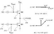
최근에는 위의 문제점을 해결하기 위해 폴리페이즈 필터(Poly Phase Filter)와 위상 변환 결합기를 통해 옥텟 위상을 생성하는 회로가 사용되고 있다. 도 2는 폴리페이즈 필터와 위상 변환 결합기를 통해 옥텟 위상 신호를 생성하는 회로이다. 도 2를 참조하면, RC-CR 폴리페이즈 필터(100)를 통해 90° 위상 차이가 나는 IQ 신호가 생성되며, 45°위상 변환 결합기(200)와 동위상 변환결합기(300)를 통해 옥텟 위상 (Octet-phase) 신호를 생성되는 것을 확인할 수 있다.Recently, in order to solve the above problem, a circuit that generates an octet phase through a polyphase filter and a phase shift combiner has been used. 2 is a circuit for generating an octet phase signal through a polyphase filter and a phase shift combiner. Referring to FIG. 2, an IQ signal having a 90° phase difference is generated through the RC-
도 3은 종래의 위상 변환 결합기를 나타내는 회로도이다. 도 3을 참조하면, 종래의 위상 변환 결합기는 인가된 0°와 90°의 신호를 벡터 합성하여 45°위상 신호가 생성한다. 벡터합성에 의해 45°위상의 신호가 생성되지만, 45°위상 변환 결합기와 동위상 변환결합기(동일한 신호가 인가되며, 입력과 같은 신호가 생성)의 출력간에는

본 발명은 위와 같은 문제점을 해결하기 위해 공통소스증폭기로 동작되는 트랜지스터와 공통드레인증폭기로 동작되는 트랜지스터에서 출력되는 출력신호를 합산하여 다중 위상신호를 생성하는데 그 목적이 있다.An object of the present invention is to generate a multi-phase signal by summing output signals output from a transistor operated as a common source amplifier and a transistor operated as a common drain authenticator in order to solve the above problems.
또한, 본 발명은 다이오드 연결부하를 가지는 공통소스증폭기의 이득의 비를 통해 생성된 위상신호에서 발생된 진폭의 오차를 감소시키는데 그 목적이 있다.In addition, an object of the present invention is to reduce an error in amplitude generated from a phase signal generated through a gain ratio of a common source amplifier having a diode-connected load.
또한, 본 발명의 위상 변환 결합기를 기반으로 하는 다중 위상 생성회로가 적용된 주파수 혼합기를 제공하는데 그 목적이 있다.In addition, an object of the present invention is to provide a frequency mixer to which a multi-phase generation circuit based on the phase shift combiner of the present invention is applied.
본 발명에 따른 위상 변환 결합기 기반의 저전력 고정확도 다중 위상 LO 생성회로는 위상신호가 입력되는 제1신호입력부, 또 다른 위상신호가 입력되는 제2신호입력부, 상기 위상신호를 입력받아 공통소스증폭기로 동작되는 제1트랜지스터, 상기 또 다른 위상신호를 입력받아 공통드레인증폭기로 동작되는 제2트랜지스터, 및 상기 제1트랜지스터의 드레인에서 출력되는 출력신호와 상기 제2트랜지스터의 소스에서 출력되는 또 다른 출력신호를 합산하여 변환위상신호를 생성하는 신호생성부가 포함된 위상변환결합기를 포함한다.The low-power, high-accuracy multi-phase LO generation circuit based on the phase shift combiner according to the present invention includes a first signal input unit to which a phase signal is input, a second signal input unit to which another phase signal is input, and a common source amplifier by receiving the phase signal. A first transistor to be operated, a second transistor to be operated as a common drain aerator by receiving the another phase signal, an output signal output from the drain of the first transistor and another output signal output from the source of the second transistor It includes a phase shift combiner including a signal generator for generating a converted phase signal by summing.
본 발명에 따른 상기 위상변환결합기는 상기 제1트랜지스터가 상기 공통소스증폭기로 동작되고, 상기 제2트랜지스터 가 상기 공통드레인증폭기로 동작됨에 따라 발생되는 출력신호간 180°위상차이로 인해 상기 제1트랜지스터의 입력 신호는 음의 신호로 입력된다.In the phase shift combiner according to the present invention, the first transistor is operated as the common source amplifier and the second transistor is operated as the common drain authentication attenuator. The input signal of is input as a negative signal.
본 발명에 따른 위상 변환 결합기 기반의 저전력 고정확도 다중 위상 LO 생성회로는 위상 차이가 나는 IQ신호를 생성하기 위한 폴리페이즈필터, 및 상기 위상변환결합기와 동일한 구성으로 이루어지며, 상기 제1신호입력부와 상기 제2신호입력부에 동일한 위상신호가 입력되는 동위상변환결합기를 더 포함한다.The low-power, high-accuracy multi-phase LO generation circuit based on the phase shift combiner according to the present invention has a polyphase filter for generating an IQ signal having a phase difference, and the same configuration as the phase shift combiner, and the first signal input unit and The second signal input unit further includes an in-phase conversion combiner for inputting the same phase signal.
본 발명에 따른 상기 위상변환결합기 및 상기 동위상변환결합기는 다이오드 연결부하를 가지는 또 다른 공통소스증폭기의 이득의 비를 통해 상기 변환위상신호에서 발생된 진폭의 오차를 감소시키는 제1진폭오차감소부가 포함된 진폭조절부를 포함한다.The phase shift combiner and the in-phase shift combiner according to the present invention have a first amplitude error reduction unit for reducing an error in amplitude generated from the converted phase signal through a gain ratio of another common source amplifier having a diode-connected load. Includes an included amplitude control unit.
본 발명은 상기 다이오드 연결부하를 가지는 또 다른 공통소스증폭기의 이득은 상기 제1트랜지스터와 상기 제2 트랜지스터의 채널 너비의 비로 조절된다.In the present invention, the gain of another common source amplifier having the diode connection load is adjusted by a ratio of the channel width of the first transistor and the second transistor.
본 발명에 따른 , 상기 진폭조절부는 상기 제1진폭감소부와 동일한 구성으로 이루어지되, 상기 제1오차감소부에 의해 상기 감소된 진폭의 오차를 유지하면서 위상 오차를 이차적으로 감소시키는 제2위상오차감소부를 더 포함한다.According to the present invention, the amplitude control unit has the same configuration as the first amplitude reduction unit, but the second phase error secondaryly reduces the phase error while maintaining the error of the reduced amplitude by the first error reduction unit. It further includes a reduction part.
본 발명에 따른 다중 위상 생성회로는 상기 다중 위상 생성회로에서 생성되는 상기 다중 위상 신호를 필요로 하는 IQ회로, 주파수 혼합기(믹서)에 적용 가능하다.The multi-phase generating circuit according to the present invention is applicable to an IQ circuit and a frequency mixer (mixer) that require the multi-phase signal generated by the multi-phase generating circuit.
본 발명은 공통소스증폭기로 동작되는 트랜지스터와 공통드레인증폭기로 동작되는 트랜지스터에서 출력되는 출력신호를 합산하여 다중 위상신호를 생성함으로서, 저전압으로 사용할 수 있는 효과가 있다.According to the present invention, a multi-phase signal is generated by summing output signals output from a transistor operated as a common source amplifier and a transistor operated as a common drain authentication amplifier, thereby making it possible to use a low voltage.
또한, 본 발명은 다이오드 연결부하를 가지는 공통소스증폭기의 이득의 비를 통해 생성된 위상신호에서 발생된 진폭의 오차를 감소시킴으로서, PVT (Process, Voltage, Temperature) 등 외부환경에 유리한 위상 변환 결합기를 제공할 수 있다.In addition, the present invention reduces the error of the amplitude generated in the phase signal generated through the ratio of the gain of the common source amplifier having a diode-connected load, thereby reducing the phase conversion combiner that is advantageous for external environments such as PVT (Process, Voltage, Temperature). Can provide.
또한, 본 발명의 위상 변환 결합기를 기반으로 하는 다중 위상 생성회로를 통해 저전력, 고정확도의 주파수 혼합기를 제공할 수 있는 효과가 있다.In addition, it is possible to provide a low-power, high-accuracy frequency mixer through a multi-phase generation circuit based on the phase shift combiner of the present invention.
도 1은 종래의 I/Q 경로에 대한 서브-하모닉 믹서를 나타내는 도면이다.
도 2는 폴리페이즈 필터와 위상 변환 결합기를 통해 옥텟 위상 신호를 생성하는 회로이다.
도 3은 종래의 위상 변환 결합기를 나타내는 회로도이다.
도 4는 본 발명에 따른 위상 변환 결합기를 나타내는 회도로이다.
도 5는 본 발명에 따른 위상 변환 결합기에서 생성된 위상신호의 진폭 오차를 감소시키는 진폭조절부를 나타내는 회로도이다.
도 6은 본 발명에서 제안하는 위상 변환 결합기의 시뮬레이션 결과를 나타내는 도면이다.
도 7은 본 발명에서 제안하는 위상 변환 결합기에 대한 Monte Carlo 시뮬레이션 결과를 나타내는 도면이다.1 is a diagram illustrating a conventional sub-harmonic mixer for an I/Q path.
2 is a circuit for generating an octet phase signal through a polyphase filter and a phase shift combiner.
3 is a circuit diagram showing a conventional phase shift combiner.
4 is a circuit diagram showing a phase shift combiner according to the present invention.
5 is a circuit diagram showing an amplitude adjusting unit for reducing an amplitude error of a phase signal generated by a phase conversion combiner according to the present invention.
6 is a diagram showing a simulation result of the phase shift combiner proposed in the present invention.
7 is a diagram showing Monte Carlo simulation results for the phase shift combiner proposed in the present invention.
이하, 본 발명의 바람직한 실시 예에 대하여 첨부된 도면을 참조하여 상세히 설명하기로 한다. 본 발명의 실시 예를 설명함에 있어서 관련된 공지 기술에 대한 구체적인 설명이 본 발명의 요지를 불필요하게 흐릴 수 있다고 판단되는 경우에 그 상세한 설명을 생략하기로 한다.Hereinafter, preferred embodiments of the present invention will be described in detail with reference to the accompanying drawings. In describing an embodiment of the present invention, when it is determined that a detailed description of a related known technology may unnecessarily obscure the subject matter of the present invention, a detailed description thereof will be omitted.
도 2는 폴리페이즈 필터와 위상 변환 결합기를 통해 옥텟 위상 신호를 생성하는 회로의 일 실시예이다. 본 발명의 다중 위상 생성회로는 도 2와 구조와 동일하게 폴리페이즈 필터(100), 위상 변환 결합기(200), 및 동위상 변환결합기(300)로 이루어진다. 도 2의 폴리페이즈 필터(100)는 90°의 위상 차이가 나는 IQ신호를 생성하기 위한 장치이며, 공지된 기술로 자세한 설명은 생략한다.2 is an embodiment of a circuit for generating an octet phase signal through a polyphase filter and a phase shift combiner. The multi-phase generation circuit of the present invention includes a
도 4는 본 발명에 따른 위상 변환 결합기를 나타내는 회도로이다. 위상 변환 결합기(200)는 폴리페이즈 필터(100)에서 생성된 위상 신호를 인가받으며, 도 2와 같이 0°, 90°, 180°, 270°의 위상신호를 입력받는다.4 is a circuit diagram showing a phase shift combiner according to the present invention. The phase shift combiner 200 receives the phase signal generated by the
도 4를 참조하면, 위상 변환 결합기(200)의 주요구성으로는 제1신호입력부(210), 제2신호입력부(220), 제1트랜지스터(211), 제2트랜지스터(221), 제1바이어스 저항(212). 제2바이어스 저항(222), 신호생성부(230)을 포함할 수 있다.Referring to FIG. 4, the phase shift combiner 200 includes a first
제1신호입력부(210)는 폴리페이즈 필터(100)로부터 위상 신호를 입력받으며, 제2신호입력부(220)는 폴리페이즈 필터(100)로부터 또 다른 위상신호를 입력받는다. 이하 위상신호가 0°, 또 다른 위상신호가 90°인 경우를 실시 예로 설명한다.The first
도 4를 참조하면, 제1바이어스 저항(212)은 제1트랜지스터(211)의 게이트(gate)에 연결되며, 제1트랜지스터(211)는 드레인(drain) 단자에서 출력이 얻어지는 공통소스증폭기(CS증폭기)로 동작된다. 제2바이어스 저항(222)은 제2트랜지스터(221)의 게이트(gate)에 연결되며, 제2트랜지스터(221)는 소스(source) 단자에서 출력이 얻어지는 공통드레인증폭기(CD증폭기)로 동작된다. 따라서 각각의 트랜지스터에서 출력은 180°위상차이를 가지게 되며, 제1트랜지스터(211)에 입력되는 위상신호는 180°의 위상 차이를 가지는 음의 신호로 입력된다.4, a
도 4에서 제1트랜지스터(211)와 제2트랜지스터(221)에 흐르는 드레인 전류는 각각


동위상 변환 결합기(300)는 위상 변환 결합기(200)와 동일한 구성으로 이루어지며, 제1신호입력부와 제2신호입력부에 180°위상차이의 신호가 입력된다. 위상 신호 -V1= -Acos(ωt+0°) = Acos(ωt+180°) 이고, 위상 신호 V2 = Acos(ωt+0°) 일 때, Vout= A(2*cos (
위와 같이 위상 변환 결합기(200)와 동위상 변환 결합기(200)에서 출력되는 위상의 차이는 45°이며, 진폭의 차이는
도 5는 본 발명에 따른 위상신호에서 발생된 진폭의 오차를 감소시키는 위한 진폭조절부를 나타내는 회로도이다. 도 5를 참조하면, 진폭조절부는 4개의 트랜지스터(231, 232, 241, 242)로 구성된다. 편의상 순차적으로 제1조절트랜지스터(231) 내지 제4 조절트랜지스터(242)로 지칭한다. 제1조절트랜지스터(231) 및 제2조절트랜지스터(232)는 제1진폭오차감소부가 되며, 3조절트랜지스터(241) 및 제4조절트랜지스터(242)는 제2위상오차감소부가 된다.5 is a circuit diagram showing an amplitude adjusting unit for reducing an error in amplitude generated from a phase signal according to the present invention. Referring to FIG. 5, the amplitude control unit is composed of four
제1진폭오차감소부는 다이오드 연결부하를 가지는 공통소스증폭기의 이득의 비를 통해 변환위상신호에서 발생된 진폭의 오차를 감소시킨다. 도 4를 참조하면, 다이오드 연결부하를 가지는 공통소스증폭기의 이득은 너비(Width)의 비로 조절되며, 너비(Width)를 α만큼 조절함으로서 진폭 오차를 줄이게 된다. Av =

제2위상오차감소부는 제1진폭감소부와 동일한 구성으로 이루어지되, 제1오차감소부에 의해 감소된 진폭의 오차를 유지하면서 위상 오차를 감소시키는 장치이다. 제2위상오차감소부는 제3 조절트랜지스터(241)와 제4 조절트랜지스터(242)로 이루어진다. 제1진폭오차감소부에서 진폭오차를 0,1mV 수준으로 맞춘다면 위상 오차가 0.1°정도 생기게 되며, 제2위상오차감소부에 의해 0.1°의 위상 오차가 더욱 감소하게 된다The second phase error reduction unit has the same configuration as the first amplitude reduction unit, but is a device that reduces the phase error while maintaining the error of the amplitude reduced by the first error reduction unit. The second phase error reduction unit includes a
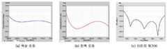
도 6은 본 발명에서 제안하는 위상 변환 결합기의 시뮬레이션 결과를 나타내는 도면이다. 도 6을 참조하면 400MHz에서 이득 오차는 0.1mV, 위상 오차는 1m°, 이미지 제거비는 84dB를 나타내며, 오차가 매우 적은 것으로 확인되었다. 도 7은 본 발명에서 제안하는 위상 변환 결합기에 대한 Monte Carlo 시뮬레이션 결과를 나타내는 도면이다. Monte Carlo 시뮬레이션을 통해 PVT(Process, Voltage, Temperature)변화에 얼마나 둔감한지를 확인할 수 있으며, Process 및 Mismatch를 고려하여 총 500회 구현하였다. 시뮬레이션 한 결과, 최대 위상 오차는 0.46°, 최대 진폭 오차는 5.5mV로 관측되었다. 또한, 500회 모두 40dB 이상의 이미지 제거량을 보장해주는 성능으로 종래의 회로(위상 오차 약 1.5°, 진폭 약 35mV)와 대비했을 때 PVT에 매우 둔감함을 확인할 수 있다.6 is a diagram showing a simulation result of the phase shift combiner proposed in the present invention. Referring to FIG. 6, at 400MHz, a gain error of 0.1mV, a phase error of 1m°, and an image rejection ratio of 84dB were found to be very small. 7 is a diagram showing Monte Carlo simulation results for the phase shift combiner proposed in the present invention. Through Monte Carlo simulation, it is possible to check how insensitive to PVT (Process, Voltage, Temperature) changes, and implemented a total of 500 times in consideration of Process and Mismatch. As a result of the simulation, the maximum phase error was observed to be 0.46° and the maximum amplitude error was 5.5 mV. In addition, it can be seen that it is very insensitive to PVT when compared to conventional circuits (phase error of about 1.5°, amplitude of about 35mV) with the ability to guarantee an image removal amount of 40dB or more in all 500 times.
본 발명에서 제안하는 다중 위상 생성회로는 종래의 주파수 혼합기(믹서)에 적용 가능하다. 주파수 혼합기(믹서)는 인가되는 다중 위상 신호를 통해 무선 주파수입력 신호를 하향 주파수로 변환하는 서브-하모닉 믹서, 다중 위상 신호를 각각의 믹서에 인가한 후 합산하여 주파수 신호로 출력하는 하모닉 제거 믹서, 스퓨리어스 이미지 응답(spurious response)을 감소시키는 이미지 제거 믹서(image reject mixer) 등 다양한 종류의 주파수 혼합기로 구성된다. 이러한 주파수 혼합기는 다중 위상신호를 필요로 하며, 본 발명에서 제안하는 다중 위상 생성회로를 적용함으로서, 저전력, 고정확도의 주파수 혼합기를 제작할 수 있다.The multi-phase generation circuit proposed in the present invention can be applied to a conventional frequency mixer (mixer). The frequency mixer (mixer) is a sub-harmonic mixer that converts a radio frequency input signal to a downlink frequency through an applied multi-phase signal, a harmonic removal mixer that applies a multi-phase signal to each mixer and then sums it up and outputs a frequency signal. It consists of various types of frequency mixers, such as an image reject mixer that reduces the spurious response. Such a frequency mixer requires a multi-phase signal, and by applying the multi-phase generation circuit proposed in the present invention, a low-power, high-accuracy frequency mixer can be manufactured.
또한, 본 발명은 RF통신에서 보편적으로 사용되는 45°위상 차이를 가지는 옥텟 위상 (Octet-phase)에 대해서만 기재되었으나. 옥텟 위상보다 더 많은 다중 위상을 가지는 신호 생성에도 응용될 수 있다.In addition, the present invention has been described only for an octet-phase having a 45° phase difference that is commonly used in RF communication. It can also be applied to signal generation with multiple phases more than octet phase.
100 : 폴리페이즈 필터 200 : 위상 변환 결합기
210 : 제1신호입력부211 : 제1트랜지스터
212 : 제1바이어스 저항220 : 제2신호입력부
221 : 제2트랜지스터222 : 제2바이어스 저항
230 : 신호생성부231 : 제1조절트랜지스터
232 : 제2조절트랜지스터241 : 제3조절트랜지스터
242 : 제4조절트랜지스터300 : 동위상 변환 결합기100: polyphase filter 200: phase shift combiner
210: first signal input unit 211: first transistor
212: first bias resistance 220: second signal input unit
221: second transistor 222: second bias resistance
230: signal generation unit 231: first control transistor
232: second control transistor 241: third control transistor
242: fourth control transistor 300: in-phase conversion coupler
Claims (7)
Translated fromKorean또 다른 위상신호가 입력되는 제2신호입력부;
상기 위상신호를 입력받아 공통소스증폭기로 동작되는 제1트랜지스터;
상기 또 다른 위상신호를 입력받아 공통드레인증폭기로 동작되는 제2트랜지스터; 및
상기 제1트랜지스터의 드레인에서 출력되는 출력신호와 상기 제2트랜지스터의 소스에서 출력되는 또 다른 출력신호를 합산하여 변환위상신호를 생성하는 신호생성부; 및 다이오드 연결부하를 가지는 또 다른 공통소스증폭기의 이득의 비를 통해 상기 변환위상신호에서 발생된 진폭의 오차를 감소시키는 제1진폭오차감소부를 포함하는 진폭조절부;가 포함된 위상변환결합기;를 포함하는 것을 특징으로 하는 위상 변환 결합기 기반의 저전력 고정확도 다중 위상 LO 생성회로.
A first signal input unit to which a phase signal is input;
A second signal input unit to which another phase signal is input;
A first transistor that receives the phase signal and operates as a common source amplifier;
A second transistor that receives the another phase signal and operates as a common drain authentication aerator; And
A signal generator configured to generate a converted phase signal by summing an output signal output from a drain of the first transistor and another output signal output from a source of the second transistor; And an amplitude adjusting unit including a first amplitude error reducing unit for reducing an error in amplitude generated in the converted phase signal through a gain ratio of another common source amplifier having a diode connection load; A low-power, high-accuracy multi-phase LO generation circuit based on a phase shift combiner, comprising:
상기 제1트랜지스터가 상기 공통소스증폭기로 동작하고, 상기 제2트랜지스터가 상기 공통드레인증폭기로 동작됨에 따라 발생되는 출력신호의 위상차이로 인해 상기 위상신호 및 상기 또 다른 위상신호가 90도 위상차이를 가지고 입력되는 것을 특징으로 하는 위상 변환 결합기 기반의 저전력 고정확도 다중 위상 LO 생성회로.
The method of claim 1, wherein the phase shift combiner
The phase signal and the other phase signal have a phase difference of 90 degrees due to a phase difference between the output signal generated when the first transistor operates as the common source amplifier and the second transistor operates as the common drain authentication aerator. A low-power, high-accuracy multi-phase LO generation circuit based on a phase-shifting combiner, characterized in that the input is carried out.
위상 차이가 나는 IQ 신호를 생성하기 위한 폴리페이즈 필터; 및
상기 위상변환결합기와 동일한 구성으로 이루어지며, 상기 제1신호입력부와 상기 제2신호입력부에 180도 위상차이를 가지는 신호가 입력되는 동위상변환결합기;를 더 포함하는 것을 특징으로 하는 위상 변환 결합기 기반의 저전력 고정확도 다중 위상 LO 생성회로.
The method of claim 2,
A polyphase filter for generating an IQ signal having a phase difference; And
The phase shift combiner-based phase shift combiner further comprises a phase shift combiner having the same configuration as the phase shift combiner and inputting a signal having a phase difference of 180 degrees to the first signal input section and the second signal input section. Low-power, high-accuracy multi-phase LO generation circuit.
상기 다이오드 연결부하를 가지는 또 다른 공통소스증폭기의 이득이 상기 제1트랜지스터와 상기 제2 트랜지스터의 채널 너비의 비로 조절하는 것을 특징으로 하는 위상 변환 결합기 기반의 저전력 고정확도 다중 위상 LO 생성회로.
The method of claim 1,
A low-power, high-accuracy multi-phase LO generation circuit based on a phase shift combiner, characterized in that the gain of another common source amplifier having the diode connection load is adjusted by a ratio of a channel width of the first transistor and the second transistor.
상기 제1진폭오차감소부와 동일한 구성으로 이루어지되, 상기 제1진폭오차감소부에 의해 상기 감소된 진폭의 오차를 유지하면서 위상 오차를 이차적으로 감소시키는 제2위상오차감소부를 더 포함하는 것을 특징으로 하는 위상 변환 결합기 기반의 저전력 고정확도 다중 위상 LO 생성회로
The method of claim 1, wherein the amplitude control unit
And a second phase error reduction unit configured to have the same configuration as the first amplitude error reduction unit, and to secondaryly reduce a phase error while maintaining an error of the reduced amplitude by the first amplitude error reduction unit. Low-power, high-accuracy multi-phase LO generation circuit based on a phase shift combiner
Priority Applications (1)
| Application Number | Priority Date | Filing Date | Title |
|---|---|---|---|
| KR1020180173374AKR102147585B1 (en) | 2018-12-31 | 2018-12-31 | Phase Shifting Adder-Based Low Power High Accuracy Multi-Phase LO Generation Circuit and Its Application For Mixer |
Applications Claiming Priority (1)
| Application Number | Priority Date | Filing Date | Title |
|---|---|---|---|
| KR1020180173374AKR102147585B1 (en) | 2018-12-31 | 2018-12-31 | Phase Shifting Adder-Based Low Power High Accuracy Multi-Phase LO Generation Circuit and Its Application For Mixer |
Publications (2)
| Publication Number | Publication Date |
|---|---|
| KR20200082625A KR20200082625A (en) | 2020-07-08 |
| KR102147585B1true KR102147585B1 (en) | 2020-08-24 |
Family
ID=71600665
Family Applications (1)
| Application Number | Title | Priority Date | Filing Date |
|---|---|---|---|
| KR1020180173374AActiveKR102147585B1 (en) | 2018-12-31 | 2018-12-31 | Phase Shifting Adder-Based Low Power High Accuracy Multi-Phase LO Generation Circuit and Its Application For Mixer |
Country Status (1)
| Country | Link |
|---|---|
| KR (1) | KR102147585B1 (en) |
Citations (1)
| Publication number | Priority date | Publication date | Assignee | Title |
|---|---|---|---|---|
| US20080032656A1 (en)* | 2004-08-02 | 2008-02-07 | Semiconductor Ideas To The Market (Itom) Bv | Controllable Power Operational Transconductance Amplifier |
Family Cites Families (1)
| Publication number | Priority date | Publication date | Assignee | Title |
|---|---|---|---|---|
| US7483678B2 (en)* | 2005-09-27 | 2009-01-27 | Skyworks Solutions, Inc. | Single chip GSM/EDGE transceiver architecture with closed loop power control |
- 2018
- 2018-12-31KRKR1020180173374Apatent/KR102147585B1/enactiveActive
Patent Citations (1)
| Publication number | Priority date | Publication date | Assignee | Title |
|---|---|---|---|---|
| US20080032656A1 (en)* | 2004-08-02 | 2008-02-07 | Semiconductor Ideas To The Market (Itom) Bv | Controllable Power Operational Transconductance Amplifier |
Also Published As
| Publication number | Publication date |
|---|---|
| KR20200082625A (en) | 2020-07-08 |
Similar Documents
| Publication | Publication Date | Title |
|---|---|---|
| US6560449B1 (en) | Image-rejection I/Q demodulators | |
| KR100533626B1 (en) | Quadrature signal generator with feedback type frequency doubler | |
| CN106603072B (en) | Injection locked ring oscillator circuit with analog quadrature calibration loop | |
| US7817970B2 (en) | Transmitting/receiving device having a polar modulator with variable predistortion | |
| US6850749B2 (en) | Local oscillator architecture to reduce transmitter pulling effect and minimize unwanted sideband | |
| US7471939B2 (en) | Multiplier and radio communication apparatus using the same | |
| US6091303A (en) | Method and apparatus for reducing oscillator noise by noise-feedforward | |
| KR102492442B1 (en) | Method and apparatus to detect lo leakage and image rejection using a single transistor | |
| US8384485B2 (en) | Reducing spurs in injection-locked oscillators | |
| KR100463792B1 (en) | Frequency converter, quadrature demodulator and quadrature modulator | |
| US8552790B2 (en) | Harmonic rejection of signal converting device and method thereof | |
| US8718576B2 (en) | Radio frequency modulator and method thereof | |
| US10897228B1 (en) | Systems and methods for detecting local oscillator leakage and image tone in I/Q mixer based transceivers | |
| US8947151B2 (en) | Frequency mixing circuit and method for suppressing local oscillation leakage in frequency mixing circuit | |
| US6785528B2 (en) | Quadrature divider | |
| US7319366B2 (en) | Offset local oscillator without using frequency divider | |
| US20090039943A1 (en) | Mixer and transceiver having the mixer | |
| US9270300B2 (en) | Radio frequency signal transmission method and device | |
| KR102147585B1 (en) | Phase Shifting Adder-Based Low Power High Accuracy Multi-Phase LO Generation Circuit and Its Application For Mixer | |
| US7848453B2 (en) | Independent LO IQ tuning for improved image rejection | |
| US8344818B1 (en) | Single side band (SSB) mixer | |
| US9264076B2 (en) | Signal generation device | |
| US6480046B1 (en) | Transmitter apparatus and methods using frequency doubling modulation | |
| US12388451B2 (en) | Analog tracking circuit to improve dynamic and static image rejection of a frequency converter | |
| JP2005260787A (en) | Phase shifter |
Legal Events
| Date | Code | Title | Description |
|---|---|---|---|
| PA0109 | Patent application | Patent event code:PA01091R01D Comment text:Patent Application Patent event date:20181231 | |
| PA0201 | Request for examination | ||
| PE0902 | Notice of grounds for rejection | Comment text:Notification of reason for refusal Patent event date:20200331 Patent event code:PE09021S01D | |
| PG1501 | Laying open of application | ||
| E701 | Decision to grant or registration of patent right | ||
| PE0701 | Decision of registration | Patent event code:PE07011S01D Comment text:Decision to Grant Registration Patent event date:20200813 | |
| GRNT | Written decision to grant | ||
| PR0701 | Registration of establishment | Comment text:Registration of Establishment Patent event date:20200818 Patent event code:PR07011E01D | |
| PR1002 | Payment of registration fee | Payment date:20200818 End annual number:3 Start annual number:1 | |
| PG1601 | Publication of registration | ||
| PR1001 | Payment of annual fee | Payment date:20230713 Start annual number:4 End annual number:4 | |
| PR1001 | Payment of annual fee | Payment date:20240730 Start annual number:5 End annual number:5 |