KR102143468B1 - Electromagnetic radiation detector based on wafer bonding - Google Patents
Electromagnetic radiation detector based on wafer bondingDownload PDFInfo
- Publication number
- KR102143468B1 KR102143468B1KR1020197028747AKR20197028747AKR102143468B1KR 102143468 B1KR102143468 B1KR 102143468B1KR 1020197028747 AKR1020197028747 AKR 1020197028747AKR 20197028747 AKR20197028747 AKR 20197028747AKR 102143468 B1KR102143468 B1KR 102143468B1
- Authority
- KR
- South Korea
- Prior art keywords
- wafer
- absorber
- layer
- forming
- read
- Prior art date
- Legal status (The legal status is an assumption and is not a legal conclusion. Google has not performed a legal analysis and makes no representation as to the accuracy of the status listed.)
- Expired - Fee Related
Links
Images


Classifications
- H—ELECTRICITY
- H10—SEMICONDUCTOR DEVICES; ELECTRIC SOLID-STATE DEVICES NOT OTHERWISE PROVIDED FOR
- H10F—INORGANIC SEMICONDUCTOR DEVICES SENSITIVE TO INFRARED RADIATION, LIGHT, ELECTROMAGNETIC RADIATION OF SHORTER WAVELENGTH OR CORPUSCULAR RADIATION
- H10F39/00—Integrated devices, or assemblies of multiple devices, comprising at least one element covered by group H10F30/00, e.g. radiation detectors comprising photodiode arrays
- H10F39/10—Integrated devices
- H10F39/12—Image sensors
- H10F39/18—Complementary metal-oxide-semiconductor [CMOS] image sensors; Photodiode array image sensors
- H10F39/184—Infrared image sensors
- H—ELECTRICITY
- H10—SEMICONDUCTOR DEVICES; ELECTRIC SOLID-STATE DEVICES NOT OTHERWISE PROVIDED FOR
- H10F—INORGANIC SEMICONDUCTOR DEVICES SENSITIVE TO INFRARED RADIATION, LIGHT, ELECTROMAGNETIC RADIATION OF SHORTER WAVELENGTH OR CORPUSCULAR RADIATION
- H10F39/00—Integrated devices, or assemblies of multiple devices, comprising at least one element covered by group H10F30/00, e.g. radiation detectors comprising photodiode arrays
- H10F39/80—Constructional details of image sensors
- H10F39/809—Constructional details of image sensors of hybrid image sensors
- H01L27/14634—
- G—PHYSICS
- G01—MEASURING; TESTING
- G01N—INVESTIGATING OR ANALYSING MATERIALS BY DETERMINING THEIR CHEMICAL OR PHYSICAL PROPERTIES
- G01N23/00—Investigating or analysing materials by the use of wave or particle radiation, e.g. X-rays or neutrons, not covered by groups G01N3/00 – G01N17/00, G01N21/00 or G01N22/00
- G01N23/02—Investigating or analysing materials by the use of wave or particle radiation, e.g. X-rays or neutrons, not covered by groups G01N3/00 – G01N17/00, G01N21/00 or G01N22/00 by transmitting the radiation through the material
- G01N23/04—Investigating or analysing materials by the use of wave or particle radiation, e.g. X-rays or neutrons, not covered by groups G01N3/00 – G01N17/00, G01N21/00 or G01N22/00 by transmitting the radiation through the material and forming images of the material
- G01N23/046—Investigating or analysing materials by the use of wave or particle radiation, e.g. X-rays or neutrons, not covered by groups G01N3/00 – G01N17/00, G01N21/00 or G01N22/00 by transmitting the radiation through the material and forming images of the material using tomography, e.g. computed tomography [CT]
- H—ELECTRICITY
- H01—ELECTRIC ELEMENTS
- H01L—SEMICONDUCTOR DEVICES NOT COVERED BY CLASS H10
- H01L23/00—Details of semiconductor or other solid state devices
- H01L23/544—Marks applied to semiconductor devices or parts, e.g. registration marks, alignment structures, wafer maps
- H01L27/14638—
- H01L27/1464—
- H01L27/14659—
- H01L27/14661—
- H01L27/1469—
- H—ELECTRICITY
- H10—SEMICONDUCTOR DEVICES; ELECTRIC SOLID-STATE DEVICES NOT OTHERWISE PROVIDED FOR
- H10F—INORGANIC SEMICONDUCTOR DEVICES SENSITIVE TO INFRARED RADIATION, LIGHT, ELECTROMAGNETIC RADIATION OF SHORTER WAVELENGTH OR CORPUSCULAR RADIATION
- H10F30/00—Individual radiation-sensitive semiconductor devices in which radiation controls the flow of current through the devices, e.g. photodetectors
- H10F30/20—Individual radiation-sensitive semiconductor devices in which radiation controls the flow of current through the devices, e.g. photodetectors the devices having potential barriers, e.g. phototransistors
- H10F30/21—Individual radiation-sensitive semiconductor devices in which radiation controls the flow of current through the devices, e.g. photodetectors the devices having potential barriers, e.g. phototransistors the devices being sensitive to infrared, visible or ultraviolet radiation
- H10F30/22—Individual radiation-sensitive semiconductor devices in which radiation controls the flow of current through the devices, e.g. photodetectors the devices having potential barriers, e.g. phototransistors the devices being sensitive to infrared, visible or ultraviolet radiation the devices having only one potential barrier, e.g. photodiodes
- H10F30/225—Individual radiation-sensitive semiconductor devices in which radiation controls the flow of current through the devices, e.g. photodetectors the devices having potential barriers, e.g. phototransistors the devices being sensitive to infrared, visible or ultraviolet radiation the devices having only one potential barrier, e.g. photodiodes the potential barrier working in avalanche mode, e.g. avalanche photodiodes
- H—ELECTRICITY
- H10—SEMICONDUCTOR DEVICES; ELECTRIC SOLID-STATE DEVICES NOT OTHERWISE PROVIDED FOR
- H10F—INORGANIC SEMICONDUCTOR DEVICES SENSITIVE TO INFRARED RADIATION, LIGHT, ELECTROMAGNETIC RADIATION OF SHORTER WAVELENGTH OR CORPUSCULAR RADIATION
- H10F39/00—Integrated devices, or assemblies of multiple devices, comprising at least one element covered by group H10F30/00, e.g. radiation detectors comprising photodiode arrays
- H10F39/011—Manufacture or treatment of image sensors covered by group H10F39/12
- H10F39/014—Manufacture or treatment of image sensors covered by group H10F39/12 of CMOS image sensors
- H—ELECTRICITY
- H10—SEMICONDUCTOR DEVICES; ELECTRIC SOLID-STATE DEVICES NOT OTHERWISE PROVIDED FOR
- H10F—INORGANIC SEMICONDUCTOR DEVICES SENSITIVE TO INFRARED RADIATION, LIGHT, ELECTROMAGNETIC RADIATION OF SHORTER WAVELENGTH OR CORPUSCULAR RADIATION
- H10F39/00—Integrated devices, or assemblies of multiple devices, comprising at least one element covered by group H10F30/00, e.g. radiation detectors comprising photodiode arrays
- H10F39/011—Manufacture or treatment of image sensors covered by group H10F39/12
- H10F39/018—Manufacture or treatment of image sensors covered by group H10F39/12 of hybrid image sensors
- H—ELECTRICITY
- H10—SEMICONDUCTOR DEVICES; ELECTRIC SOLID-STATE DEVICES NOT OTHERWISE PROVIDED FOR
- H10F—INORGANIC SEMICONDUCTOR DEVICES SENSITIVE TO INFRARED RADIATION, LIGHT, ELECTROMAGNETIC RADIATION OF SHORTER WAVELENGTH OR CORPUSCULAR RADIATION
- H10F39/00—Integrated devices, or assemblies of multiple devices, comprising at least one element covered by group H10F30/00, e.g. radiation detectors comprising photodiode arrays
- H10F39/011—Manufacture or treatment of image sensors covered by group H10F39/12
- H10F39/021—Manufacture or treatment of image sensors covered by group H10F39/12 of image sensors having active layers comprising only Group III-V materials, e.g. GaAs, AlGaAs or InP
- H—ELECTRICITY
- H10—SEMICONDUCTOR DEVICES; ELECTRIC SOLID-STATE DEVICES NOT OTHERWISE PROVIDED FOR
- H10F—INORGANIC SEMICONDUCTOR DEVICES SENSITIVE TO INFRARED RADIATION, LIGHT, ELECTROMAGNETIC RADIATION OF SHORTER WAVELENGTH OR CORPUSCULAR RADIATION
- H10F39/00—Integrated devices, or assemblies of multiple devices, comprising at least one element covered by group H10F30/00, e.g. radiation detectors comprising photodiode arrays
- H10F39/011—Manufacture or treatment of image sensors covered by group H10F39/12
- H10F39/022—Manufacture or treatment of image sensors covered by group H10F39/12 of image sensors having active layers comprising only Group II-VI materials, e.g. CdS, ZnS or CdTe
- H—ELECTRICITY
- H10—SEMICONDUCTOR DEVICES; ELECTRIC SOLID-STATE DEVICES NOT OTHERWISE PROVIDED FOR
- H10F—INORGANIC SEMICONDUCTOR DEVICES SENSITIVE TO INFRARED RADIATION, LIGHT, ELECTROMAGNETIC RADIATION OF SHORTER WAVELENGTH OR CORPUSCULAR RADIATION
- H10F39/00—Integrated devices, or assemblies of multiple devices, comprising at least one element covered by group H10F30/00, e.g. radiation detectors comprising photodiode arrays
- H10F39/10—Integrated devices
- H10F39/12—Image sensors
- H10F39/18—Complementary metal-oxide-semiconductor [CMOS] image sensors; Photodiode array image sensors
- H10F39/184—Infrared image sensors
- H10F39/1843—Infrared image sensors of the hybrid type
- H—ELECTRICITY
- H10—SEMICONDUCTOR DEVICES; ELECTRIC SOLID-STATE DEVICES NOT OTHERWISE PROVIDED FOR
- H10F—INORGANIC SEMICONDUCTOR DEVICES SENSITIVE TO INFRARED RADIATION, LIGHT, ELECTROMAGNETIC RADIATION OF SHORTER WAVELENGTH OR CORPUSCULAR RADIATION
- H10F39/00—Integrated devices, or assemblies of multiple devices, comprising at least one element covered by group H10F30/00, e.g. radiation detectors comprising photodiode arrays
- H10F39/10—Integrated devices
- H10F39/12—Image sensors
- H10F39/18—Complementary metal-oxide-semiconductor [CMOS] image sensors; Photodiode array image sensors
- H10F39/189—X-ray, gamma-ray or corpuscular radiation imagers
- H10F39/1892—Direct radiation image sensors
- H—ELECTRICITY
- H10—SEMICONDUCTOR DEVICES; ELECTRIC SOLID-STATE DEVICES NOT OTHERWISE PROVIDED FOR
- H10F—INORGANIC SEMICONDUCTOR DEVICES SENSITIVE TO INFRARED RADIATION, LIGHT, ELECTROMAGNETIC RADIATION OF SHORTER WAVELENGTH OR CORPUSCULAR RADIATION
- H10F39/00—Integrated devices, or assemblies of multiple devices, comprising at least one element covered by group H10F30/00, e.g. radiation detectors comprising photodiode arrays
- H10F39/10—Integrated devices
- H10F39/12—Image sensors
- H10F39/18—Complementary metal-oxide-semiconductor [CMOS] image sensors; Photodiode array image sensors
- H10F39/189—X-ray, gamma-ray or corpuscular radiation imagers
- H10F39/1895—X-ray, gamma-ray or corpuscular radiation imagers of the hybrid type
- H—ELECTRICITY
- H10—SEMICONDUCTOR DEVICES; ELECTRIC SOLID-STATE DEVICES NOT OTHERWISE PROVIDED FOR
- H10F—INORGANIC SEMICONDUCTOR DEVICES SENSITIVE TO INFRARED RADIATION, LIGHT, ELECTROMAGNETIC RADIATION OF SHORTER WAVELENGTH OR CORPUSCULAR RADIATION
- H10F39/00—Integrated devices, or assemblies of multiple devices, comprising at least one element covered by group H10F30/00, e.g. radiation detectors comprising photodiode arrays
- H10F39/10—Integrated devices
- H10F39/12—Image sensors
- H10F39/191—Photoconductor image sensors
- H10F39/195—X-ray, gamma-ray or corpuscular radiation imagers
- H—ELECTRICITY
- H10—SEMICONDUCTOR DEVICES; ELECTRIC SOLID-STATE DEVICES NOT OTHERWISE PROVIDED FOR
- H10F—INORGANIC SEMICONDUCTOR DEVICES SENSITIVE TO INFRARED RADIATION, LIGHT, ELECTROMAGNETIC RADIATION OF SHORTER WAVELENGTH OR CORPUSCULAR RADIATION
- H10F39/00—Integrated devices, or assemblies of multiple devices, comprising at least one element covered by group H10F30/00, e.g. radiation detectors comprising photodiode arrays
- H10F39/10—Integrated devices
- H10F39/12—Image sensors
- H10F39/199—Back-illuminated image sensors
- H—ELECTRICITY
- H10—SEMICONDUCTOR DEVICES; ELECTRIC SOLID-STATE DEVICES NOT OTHERWISE PROVIDED FOR
- H10F—INORGANIC SEMICONDUCTOR DEVICES SENSITIVE TO INFRARED RADIATION, LIGHT, ELECTROMAGNETIC RADIATION OF SHORTER WAVELENGTH OR CORPUSCULAR RADIATION
- H10F39/00—Integrated devices, or assemblies of multiple devices, comprising at least one element covered by group H10F30/00, e.g. radiation detectors comprising photodiode arrays
- H10F39/80—Constructional details of image sensors
- H10F39/807—Pixel isolation structures
- H—ELECTRICITY
- H10—SEMICONDUCTOR DEVICES; ELECTRIC SOLID-STATE DEVICES NOT OTHERWISE PROVIDED FOR
- H10F—INORGANIC SEMICONDUCTOR DEVICES SENSITIVE TO INFRARED RADIATION, LIGHT, ELECTROMAGNETIC RADIATION OF SHORTER WAVELENGTH OR CORPUSCULAR RADIATION
- H10F39/00—Integrated devices, or assemblies of multiple devices, comprising at least one element covered by group H10F30/00, e.g. radiation detectors comprising photodiode arrays
- H10F39/80—Constructional details of image sensors
- H10F39/811—Interconnections
- H—ELECTRICITY
- H10—SEMICONDUCTOR DEVICES; ELECTRIC SOLID-STATE DEVICES NOT OTHERWISE PROVIDED FOR
- H10F—INORGANIC SEMICONDUCTOR DEVICES SENSITIVE TO INFRARED RADIATION, LIGHT, ELECTROMAGNETIC RADIATION OF SHORTER WAVELENGTH OR CORPUSCULAR RADIATION
- H10F39/00—Integrated devices, or assemblies of multiple devices, comprising at least one element covered by group H10F30/00, e.g. radiation detectors comprising photodiode arrays
- H10F39/80—Constructional details of image sensors
- H10F39/812—Arrangements for transferring the charges in the image sensor perpendicular to the imaging plane, e.g. buried regions used to transfer generated charges to circuitry under the photosensitive region
- H—ELECTRICITY
- H10—SEMICONDUCTOR DEVICES; ELECTRIC SOLID-STATE DEVICES NOT OTHERWISE PROVIDED FOR
- H10F—INORGANIC SEMICONDUCTOR DEVICES SENSITIVE TO INFRARED RADIATION, LIGHT, ELECTROMAGNETIC RADIATION OF SHORTER WAVELENGTH OR CORPUSCULAR RADIATION
- H10F71/00—Manufacture or treatment of devices covered by this subclass
- H10F71/121—The active layers comprising only Group IV materials
- H10F71/1215—The active layers comprising only Group IV materials comprising at least two Group IV elements, e.g. SiGe
- H—ELECTRICITY
- H10—SEMICONDUCTOR DEVICES; ELECTRIC SOLID-STATE DEVICES NOT OTHERWISE PROVIDED FOR
- H10F—INORGANIC SEMICONDUCTOR DEVICES SENSITIVE TO INFRARED RADIATION, LIGHT, ELECTROMAGNETIC RADIATION OF SHORTER WAVELENGTH OR CORPUSCULAR RADIATION
- H10F71/00—Manufacture or treatment of devices covered by this subclass
- H10F71/125—The active layers comprising only Group II-VI materials, e.g. CdS, ZnS or CdTe
- H10F71/1253—The active layers comprising only Group II-VI materials, e.g. CdS, ZnS or CdTe comprising at least three elements, e.g. HgCdTe
- H—ELECTRICITY
- H10—SEMICONDUCTOR DEVICES; ELECTRIC SOLID-STATE DEVICES NOT OTHERWISE PROVIDED FOR
- H10F—INORGANIC SEMICONDUCTOR DEVICES SENSITIVE TO INFRARED RADIATION, LIGHT, ELECTROMAGNETIC RADIATION OF SHORTER WAVELENGTH OR CORPUSCULAR RADIATION
- H10F71/00—Manufacture or treatment of devices covered by this subclass
- H10F71/127—The active layers comprising only Group III-V materials, e.g. GaAs or InP
- H10F71/1272—The active layers comprising only Group III-V materials, e.g. GaAs or InP comprising at least three elements, e.g. GaAlAs or InGaAsP
- H—ELECTRICITY
- H10—SEMICONDUCTOR DEVICES; ELECTRIC SOLID-STATE DEVICES NOT OTHERWISE PROVIDED FOR
- H10F—INORGANIC SEMICONDUCTOR DEVICES SENSITIVE TO INFRARED RADIATION, LIGHT, ELECTROMAGNETIC RADIATION OF SHORTER WAVELENGTH OR CORPUSCULAR RADIATION
- H10F71/00—Manufacture or treatment of devices covered by this subclass
- H10F71/139—Manufacture or treatment of devices covered by this subclass using temporary substrates
- H—ELECTRICITY
- H10—SEMICONDUCTOR DEVICES; ELECTRIC SOLID-STATE DEVICES NOT OTHERWISE PROVIDED FOR
- H10F—INORGANIC SEMICONDUCTOR DEVICES SENSITIVE TO INFRARED RADIATION, LIGHT, ELECTROMAGNETIC RADIATION OF SHORTER WAVELENGTH OR CORPUSCULAR RADIATION
- H10F77/00—Constructional details of devices covered by this subclass
- H10F77/10—Semiconductor bodies
- H10F77/12—Active materials
- H10F77/122—Active materials comprising only Group IV materials
- H—ELECTRICITY
- H10—SEMICONDUCTOR DEVICES; ELECTRIC SOLID-STATE DEVICES NOT OTHERWISE PROVIDED FOR
- H10F—INORGANIC SEMICONDUCTOR DEVICES SENSITIVE TO INFRARED RADIATION, LIGHT, ELECTROMAGNETIC RADIATION OF SHORTER WAVELENGTH OR CORPUSCULAR RADIATION
- H10F77/00—Constructional details of devices covered by this subclass
- H10F77/10—Semiconductor bodies
- H10F77/12—Active materials
- H10F77/123—Active materials comprising only Group II-VI materials, e.g. CdS, ZnS or HgCdTe
- H10F77/1237—Active materials comprising only Group II-VI materials, e.g. CdS, ZnS or HgCdTe having at least three elements, e.g. HgCdTe
- H—ELECTRICITY
- H10—SEMICONDUCTOR DEVICES; ELECTRIC SOLID-STATE DEVICES NOT OTHERWISE PROVIDED FOR
- H10F—INORGANIC SEMICONDUCTOR DEVICES SENSITIVE TO INFRARED RADIATION, LIGHT, ELECTROMAGNETIC RADIATION OF SHORTER WAVELENGTH OR CORPUSCULAR RADIATION
- H10F77/00—Constructional details of devices covered by this subclass
- H10F77/10—Semiconductor bodies
- H10F77/12—Active materials
- H10F77/124—Active materials comprising only Group III-V materials, e.g. GaAs
- H10F77/1248—Active materials comprising only Group III-V materials, e.g. GaAs having three or more elements, e.g. GaAlAs, InGaAs or InGaAsP
- H—ELECTRICITY
- H01—ELECTRIC ELEMENTS
- H01L—SEMICONDUCTOR DEVICES NOT COVERED BY CLASS H10
- H01L2223/00—Details relating to semiconductor or other solid state devices covered by the group H01L23/00
- H01L2223/544—Marks applied to semiconductor devices or parts
- H01L2223/54426—Marks applied to semiconductor devices or parts for alignment
- H—ELECTRICITY
- H01—ELECTRIC ELEMENTS
- H01L—SEMICONDUCTOR DEVICES NOT COVERED BY CLASS H10
- H01L2223/00—Details relating to semiconductor or other solid state devices covered by the group H01L23/00
- H01L2223/544—Marks applied to semiconductor devices or parts
- H01L2223/54493—Peripheral marks on wafers, e.g. orientation flats, notches, lot number
Landscapes
- Health & Medical Sciences (AREA)
- Physics & Mathematics (AREA)
- General Physics & Mathematics (AREA)
- Engineering & Computer Science (AREA)
- Radiology & Medical Imaging (AREA)
- Chemical & Material Sciences (AREA)
- Power Engineering (AREA)
- Computer Hardware Design (AREA)
- Nuclear Medicine, Radiotherapy & Molecular Imaging (AREA)
- Pulmonology (AREA)
- Condensed Matter Physics & Semiconductors (AREA)
- Theoretical Computer Science (AREA)
- Life Sciences & Earth Sciences (AREA)
- Microelectronics & Electronic Packaging (AREA)
- Analytical Chemistry (AREA)
- Biochemistry (AREA)
- General Health & Medical Sciences (AREA)
- Immunology (AREA)
- Pathology (AREA)
- Solid State Image Pick-Up Elements (AREA)
- Toxicology (AREA)
- Light Receiving Elements (AREA)
Abstract
Translated fromKoreanDescription
Translated fromKorean관련 출원에 대한 상호참조Cross-reference to related applications
본 출원은 본 명세서에 전문이 참조로 통합되어 있고, 2017년 3월 1일 출원된 미국 가출원 62/465,199호의 이익에 대한 우선권을 주장한다.This application is hereby incorporated by reference in its entirety and claims priority to the interests of U.S. Provisional Application No. 62/465,199, filed March 1, 2017.
본 발명은 전자기 방사선의 탐지 및 이미징(imaging)을 위한 모놀리식 CMOS(Complementary Metal Oxide Semiconductor) 집적 구조물들로부터 만들어진 화소 검출기들과 그러한 구조물들을 형성하기 위한 방법들에 관한 것이다.The present invention relates to pixel detectors made from monolithic Complementary Metal Oxide Semiconductor (CMOS) integrated structures for the detection and imaging of electromagnetic radiation and methods for forming such structures.
전자파 방사선 감지를 위한 현재의 디지털 이미징 장치(화소 검출기라고도 함)는 영향을 미치는 광자를 전기 신호로 변환하는 방식으로 구분하여 두 개의 넓은 범주로 분류할 수 있다. X선 광자를 예로 들자면, 이러한 등급 중 첫 번째 등급에서는 X선 광자가 섬광층의 가시 광자로 에너지를 먼저 하향 변환한다는 점에서 변환이 간접적으로 이루어진다. 가시 광자는 이후 일련의 광다이오드에 의해 검출되며, 여기서 전자 구멍 쌍의 광생성은 판독 전자기기에 의해 추가로 처리되고 컴퓨터 화면에 이미지로 표시되는 전기 신호를 발생시킨다. 간접 X선 이미징 장치의 2단계 변환 프로세스는 X선을 가시 광자로 변환하는 동안 발생하는 손실과 산란 때문에 그리고 그러한 광자의 검출에서 발생하는 제한된 변환 효율과 공간 분해능의 단점을 겪는다. 일반적으로 약 25개의 전자 구멍 쌍은 입사 X선 에너지의 keV 당 판독 전자기기에 의해 최종적으로 측정된다.Current digital imaging devices (also referred to as pixel detectors) for detecting electromagnetic radiation can be classified into two broad categories by dividing the photons in effect into electrical signals. Taking X-ray photons as an example, in the first of these classes, conversion is indirectly done in that X-ray photons first down-convert energy to visible photons in the scintillation layer. Visible photons are then detected by a series of photodiodes, where the photogeneration of the pair of electron holes is further processed by the reading electronics and generates an electrical signal that is displayed as an image on a computer screen. The two-step conversion process of indirect X-ray imaging devices suffers from the disadvantages of limited conversion efficiency and spatial resolution arising from the detection of such photons and because of the losses and scattering that occur during the conversion of X-rays into visible photons. Typically about 25 pairs of electron holes are finally measured by the readout electronics per keV of incident X-ray energy.
이러한 화소 검출기의 두 번째 등급에서 반도체 흡수체는 X선을 전자홀 쌍으로 직접 변환할 수 있으며, 이는 판독 전자장치에 의해 전기 신호로 측정될 수 있다. 이러한 흡수체는 섬광기 기반 간접 변환에 비해 뛰어난 감도와 높은 공간 및 시간 분해능 외에도 입사 X선 광자의 에너지가 생성되는 전자홀 쌍의 수에 비례하므로 펄스 높이 분석에 의해 측정할 수 있으므로 스펙트럼 분해능도 제공한다. 실리콘(Si)에서 단일 전자홀 쌍을 만들려면 평균 3.6 eV가 필요하다(예: R.C. 참조). 물리학의 Alig 등. B 22, 5565 (1980), 그리고 R.C. 물리학에서 알리그. B 27, 968년(1983년) 개정판, 그 전체 공시는 참조에 의해 통합된다. 이는 평균적으로 흡수된 X선 에너지의 keV당 280개의 전자홀 쌍으로 이어지며, 여기서 변환 효율이 섬광기와 포토다이오드 조합의 값을 10배 이상 초과한다는 것을 알 수 있다.In this second class of pixel detectors, semiconductor absorbers can directly convert X-rays into pairs of electron holes, which can be measured as electrical signals by readout electronics. In addition to superior sensitivity and high spatial and temporal resolution compared to scintillator-based indirect conversion, these absorbers also provide spectral resolution as the energy of incident X-ray photons is proportional to the number of electron hole pairs generated, so they can be measured by pulse height analysis. . In silicon (Si), an average of 3.6 eV is required to make a single electron hole pair (see e.g. R.C.). Alig et al. in physics.
일반적으로 반도체 흡수체에 의한 직접 변환을 사용하는 X선 영상 검출기(X-ray imaging detector) 또는 화소 센서는 다양한 방법으로 구현할 수 있다. 상용 평면 패널 제작에 사용되는 한 가지 접근방식은 박막 트랜지스터로 만든 판독 전자기기에 직접 침전된 다결정 또는 비정형 재료에 기초한다. 예를 들어 의료용 비정형 셀레늄 흡수장치가 있는 평면 패널 X선 이미징 검출기는 대규모로 제공되는 아지드를 만드는 데 비교적 저렴하다(예를 들면, S.Kasap 등의 Sensors 11, 512(2011)를 참조하라). 그러나 단결정 형태의 재료는 다결정과 비정형 재료에 비해 훨씬 우수한 운반 특성을 제공한다. 따라서 검출기 성능 향상을 제공해야 한다. 반면 단결정 흡수체는 비정형 박막 트랜지스터로 구성된 판독 전자기기와 호환되지 않는다. 그것들은 원칙적으로 CMOS 처리된 판독 웨이퍼에서 전형적으로 재배될 수 있지만, 대개 견딜 수 없을 정도로 높은 열 예산을 희생하여 높은 공정 온도와 호환되는 특별 금속화 계획을 필요로 한다(예를 들면, 본 명세서에 전문이 참조로 통합되어 있는 von Kanel에 의한 미국 특허 8,237,126호를 참조하라). 일반적으로 표준 알루미늄 금속화에서는 온도를 450℃ 이하로 유지해야 한다.In general, an X-ray imaging detector or a pixel sensor using direct conversion by a semiconductor absorber can be implemented in various ways. One approach used in commercial flat panel fabrication is based on polycrystalline or amorphous materials deposited directly into readout electronics made from thin-film transistors. For example, flat panel X-ray imaging detectors with medical atypical selenium absorbers are relatively inexpensive to make azides available on a large scale (see, for example, S. Kasap et al.,
CMOS 처리된 판독 전자제품과 호환되기 위해서는 모든 흡수장치 화소에서 전기 신호를 처리하는 데 필요한 흡수장치와 판독 웨이퍼 사이의 전기적 연결이 저온 웨이퍼 본딩 공정에 의해 실현되어야 한다. 가장 일반적인 본딩 기술은 예를 들어 Medipix 공동 작업(medipix.web.cern.ch) 또는 Dectris AG(dectris.ch)에서 사용되는 범프 본딩이다. 수 ㎠을 초과하는 검출기 영역의 범프 본딩은 비용이 많이 드는 기법일 뿐만 아니라 일반적으로 화소 크기를 약 50㎛로 제한한다. 흡수체는 원칙적으로 Si, Ge, GaA 및 CdTe 또는 CdZnTe 합금들(예를 들어, 본 명세서에 전문이 참조로 통합되고 Collins 등에 의한 유럽특허 0571135호를 참조하라)과 같이 대형 단결정들이 성장될 수 있는 활동적인 미립자 검출에 적합한 반도체 재료로 구성될 수 있다. 예를 들어 In 마이크로 범프들과의 범프 본딩은 적외선 초점 평면 배열 제작에도 사용되며, 여기서 15㎛의 화소 크기가 생산 중이고 10㎛ 이하가 실현 가능할 것으로 보인다. 일반적으로 이들 어레이는 X선 이미징에 사용되는 어레이보다 면적이 훨씬 작으며, 거의 1㎠를 초과하지 않는다(예를 들면, 본 명세서에 전문이 참조로 통합되어 있고 P Bensussan 등에 의한 SPIE의 in Proc에서의, Vol. 7298, pp. 72982N-1 내지 72982N-31(2009)를 참조하라). 적외선 이미징을 위해 InGaAs 합금, InSb, HgCdTe 합금들과 같은 추가적인 흡수체 재료가 사용되고 있다.In order to be compatible with CMOS-processed readout electronics, the electrical connection between the absorber and the readout wafer, which is required to process electrical signals in all the absorber pixels, must be realized by a low-temperature wafer bonding process. The most common bonding technique is bump bonding, for example, used by Medipix collaboration (medipix.web.cern.ch) or Dectris AG (dectris.ch). Bump bonding of the detector area exceeding several cm2 is not only an expensive technique, but also generally limits the pixel size to about 50 μm. The absorber is, in principle, an activity in which large single crystals can be grown, such as Si, Ge, GaA and CdTe or CdZnTe alloys (e.g., see European Patent 0571135 by Collins et al., incorporated herein by reference in its entirety). It may be composed of a semiconductor material suitable for detecting fine particles. Bump bonding with In micro bumps, for example, is also used to fabricate an array of infrared focal planes, where a pixel size of 15 µm is in production, and 10 µm or less is expected to be feasible. In general, these arrays are much smaller in area than arrays used for X-ray imaging and rarely exceed 1 cm2 (e.g., in Proc of SPIE by P Bensussan et al. See, Vol. 7298, pp. 72982N-1 to 72982N-31 (2009)). Additional absorber materials such as InGaAs alloys, InSb, and HgCdTe alloys are being used for infrared imaging.
대형 X선 검출기의 경우 일반적인 범프 본딩으로는 화소 크기를 약 50㎛ 미만으로 미는 것은 어렵지만, 잠재적으로 더 높은 검출기 분해능을 제공하는 다른 본딩 기술이 있다. 그 중 하나는 예를 들어 집적회로, 이른바 3D-IC 기술의 수직적 집적으로 알려져 있다. 여기서 범프 본딩은 산화물과 산화물의 융접 본딩과 산화물로 둘러싸인 금속 패드의 금속 대 금속 본딩으로 구성된다. 그 결과 구조는 실제 단일 구성과 구별할 수 없다(예를 들면, 본 명세서에 전문이 참조로 통합되어 있고 G.W. Deptuch 등에 의한 IEEE Trans에서의 Nucl. Sci 57, 2178(2010)을 참조하라). 이러한 이유로 우리는 다음과 같이 직접 웨이퍼 본딩이 마치 상형 웨이퍼 스택의 형태로 제작된 것처럼 단일 웨이퍼 본딩에 의해 만들어진 이질 구조를 고려해야 한다.For large X-ray detectors it is difficult to push the pixel size to less than about 50 μm with typical bump bonding, but there are other bonding techniques that potentially provide higher detector resolution. One of them is known for example as an integrated circuit, the vertical integration of so-called 3D-IC technology. Here, the bump bonding consists of fusion bonding of oxide and oxide and metal-to-metal bonding of a metal pad surrounded by oxide. As a result, the structure is indistinguishable from an actual single configuration (for example, see Nucl. Sci 57, 2178 (2010) in IEEE Trans, by G.W. Deptuch et al., incorporated herein by reference in its entirety). For this reason, we have to consider the heterogeneous structure made by single wafer bonding as follows, as if direct wafer bonding was made in the form of a hierarchical wafer stack.
그러나 또 다른 본딩 기법에서는 흡수체 웨이퍼와 판독 웨이퍼 사이의 저온에서 전기 전도성 공유 반도체 본드가 형성된다. 공유 반도체 본딩은 본질적으로 다시 모놀리식 구조로 이어진다(예를 들면, 본 명세서에 전문이 참조로 통합되어 있고 von Kanel에 의한 국제 특허출원 WO2016/097850호를 참조하라). 표면이 본딩 전에 각각 수소 또는 산화물로 덮여 있는 잘 알려진 소수성 및 소수성 본딩 기법과는 대조적으로, 공유 반도체 본딩은 특히 실리콘이 본딩 파트너 중 하나일 때 표면을 원자적으로 깨끗하게 할 것을 요구한다. 따라서 공유 반도체 본딩은 고진공 또는 초고진공 도구에서만 수행할 수 있다. 이상적인 상황에서 완벽하게 평평한 반도체 웨이퍼 2개가 서로 꼬이거나 기울지 않고 매우 정확하게 정렬될 때, 두 표면의 매달린 결합은 일단 두 웨이퍼가 접촉하게 되면 상형 성장 중에 형성된 결합과 구별이 불가능한 공유 결합을 형성한다. 분명히, 실제로 그러한 이상적인 상황은 결코 일어나지 않으며, 유한한 표면 거칠기와 정렬 불량은 2개의 웨이퍼가 동일한 반도체 물질로 만들어졌을 때에도 항상 유한한 개수의 계면 결함을 초래한다. 사용된 CMOS 프로세스에 따라 화소 크기는, 예를 들면 약 100㎛ 내지 200㎛, 50㎛ 내지 100㎛ 또는 20㎛ 내지 50㎛ 또는 5㎛ 내지 20㎛와 같이 넓은 범위에서 달라질 수 있다.However, in another bonding technique, an electrically conductive shared semiconductor bond is formed at low temperatures between the absorber wafer and the read wafer. Shared semiconductor bonding essentially leads back to a monolithic structure (see, for example, international patent application WO2016/097850 by von Kanel, incorporated herein by reference in its entirety). In contrast to the well-known hydrophobic and hydrophobic bonding techniques, in which the surface is covered with hydrogen or oxide, respectively, prior to bonding, covalent semiconductor bonding requires that the surface be atomically cleaned, especially when silicon is one of its bonding partners. Thus, shared semiconductor bonding can only be performed on high vacuum or ultra high vacuum tools. In an ideal situation, when two perfectly flat semiconductor wafers are aligned very accurately, without twisting or tilting each other, the hanging bonds of the two surfaces, once the two wafers come into contact, form an indistinguishable covalent bond from the bond formed during hieroglyphic growth. Obviously, in practice such an ideal situation never occurs, and finite surface roughness and misalignment always result in a finite number of interfacial defects even when two wafers are made of the same semiconductor material. Depending on the CMOS process used, the pixel size may vary in a wide range, such as about 100 μm to 200 μm, 50 μm to 100 μm, or 20 μm to 50 μm, or 5 μm to 20 μm, for example.
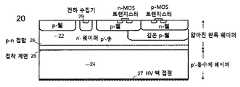
이 본딩 방식에서는 백사이드 조명에 의해 충전 캐리어(charge carrier)가 생성되며, 여기서 금속 및 유전층들 구성된 CMOS 스택의 반대쪽에 있는 판독 웨이퍼의 얇은 Si 기판에 흡수체 웨이퍼가 접합된다. 그런 다음 전하가 판독 웨이퍼에서 전하 컬렉터에 의해 수집되기 위해 공유 결합된 반도체 인터페이스를 통과해야 한다. 따라서 흡수체의 전자파 방사선에 의해 여기되는 전자-정공 쌍을 분리하는 데 필요한 전기장은 판독 웨이퍼와 흡수체 웨이퍼 사이에 존재하는 역바이어스 p-n 접합부에 의해 발생하며, 두 접점은 모두 경량 도핑형이고 반대 도핑형이다. 종래기술의 예는 도 1a 내지 도 1c에서 공칭 결합 검출기 구조 중 3가지 다른 실시예들(10, 20 및 30)을 볼 수 있다(예를 들면, 본 명세서에 전문이 참조로 통합되어 있고, von Kanel에 의한 국제 특허 출원 PCT/IB2017/001032호를 참조하라). CMOS 처리된 화소 판독 전자기기가 있는 실리콘 층(12, 22, 32)은 이들 도면에서 개략적으로 표시되며, 그 위에 있는 CMOS 스택은 산화물과 금속 층으로 구성되어 있지 않다. 판독 웨이퍼의 Si 기판은 역전압(17, 27, 37)을 p-n 접합부(16, 26, 36)에 인가하면 전하 컬렉터(19, 29, 39)에 의해 수집되고 판독 전자기기에 의해 처리되게 하기 위해, 흡수체 웨이퍼(14, 24, 34)와 함께 그것의 디플리션(deplection)을 촉진하도록 일반적으로 10㎛ 내지 20㎛까지 얇게 하여 X선 흡수에 의해 생성된 전자-정공 쌍에서 발생하는 전하가 접합된 인터페이스(18, 28, 38)를 교차할 수 있도록 얇아야 한다. 판독 웨이퍼의 Si 기판이 얇아질 수 있도록 앞면의 CMOS 스택을 먼저 평탄화하여 캐리어 웨이퍼(처리 웨이퍼(handling wafer)라고도 함)에 접합한다. 이 기계적 안정화 단계 이후, Si 기판의 뒷면은 필요한 두께로 얇아질 수 있다(예를 들면, 본 명세서에 전문이 참조로 통합되어 있고 Von Kanel에 의한 국제 특허출원 PCT/IB2017/001032호를 참조하라).In this bonding method, a charge carrier is created by backside illumination, where an absorber wafer is bonded to a thin Si substrate of a read wafer on the opposite side of a CMOS stack composed of metal and dielectric layers. The charge then has to pass through a covalently bonded semiconductor interface to be collected by the charge collector on the read wafer. Therefore, the electric field required to separate the electron-hole pairs excited by the electromagnetic radiation of the absorber is generated by the reverse bias pn junction that exists between the readout wafer and the absorber wafer, both of which are light doped and reverse doped. . As an example of the prior art, three different embodiments (10, 20 and 30) of the nominally coupled detector structure can be seen in FIGS. 1A to 1C (e.g., von See International Patent Application PCT/IB2017/001032 by Kanel).
검출기의 화소 크기는 전하 컬렉터(19, 29, 39)의 간격(spacing)에 의해 주어지며, 그 중 하나만 도 1a 내지 도 1c에 표시된다. 실시예들(10 내지 30)에서 p-n 접합은 접합된 인터페이스(도 1a, 도 1c) 또는 판독(도 1b) 또는 흡수체 웨이퍼에 바로 위치한다. 따라서 접착된 계면은 반드시 역바이어스 p-n 접합부의 디플리션 영역에 위치한다. 최적의 조건에서도 접합된 계면은 약간의 웨이퍼 정렬 불량으로 인한 이탈(dislocation)과 같은 결함을 포함한다(예를 들면, 본 명세서에 전문이 참조로 통합되어 있고 T. Akatsu 등에 의한 in J. Mat. Sci. 39, 3031(2004)를참조하라). 계면 결함은 접합된 계면을 통한 전하 전송에 부정적인 영향을 미치는 잠재적 장벽을 일으킬 수 있다(예를 들면, 본 명세서에 전문이 참조로 통합되어 있고 S. Bengtsson 등에 의한 in J. Appl. Phys, 1231(1989)를 참조하라). 더욱이 결정 결함들은 대개 밴드 갭의 전자 상태들과 관련된다. 예를 들어 p-n 접합의 디플리션 영역 내에 위치하는 경우, 역누설 전류를 강화하는 생성-재결합 센터들의 역할을 할 수 있다(예를 들면, 본 명세서에 전문이 참조로 통합되어 있고 W. Shockley 등에 의한 in Phys. Rev. 87, 835(1952)를 참조하라). 그러한 결함은 또한 스퍼터링에 의해 접합 파트너들의 표면 산화물을 제거하는 중에 발생하여 표면의 변형을 일으키며, 이는 접합된 계면에서 얇은 비형질층을 생성하게 된다(예를 들면, 본 명세서에 전문이 참조로 통합되어 있고 C. Flotgen 등에 의한 in ECS Transactions 64, 103(2014)를 참조하라). 그러한 결함과 관련된 전자 상태는 수소에 의해 어느 정도 부동태화될 수 있다(예를 들면, 본 명세서에 전문이 참조로 통합되어 있고 A. Loshackenko 등에 의한 in Phys. Status Solidi C 10, 36(2013) 및von Kanel에 의한 국제 공보 WO 2017/141103호를 참조하라). 하지만, 수소 부동태화가 가벼운 도핑된 접합 파트너들 사이의 접착된 계면을 통해 완전히 방해받지 않는 전하 전달을 야기할 것인지와, 검출기 작동 하에서 부동태화의 장기적 안정성에 대한 보증이 있을지는 확실하지 않다.The pixel size of the detector is given by the spacing of the
따라서 밴드 갭에서 결함 관련 상태에 의해 발생되는 누설 전류 증가가 발생하지 않는 공유 결합된 검출기 구조들에 대한 필요성이 존재한다. 표면 활성화 및 웨이퍼 본딩 중에 생성된 결함 상태들에 의해 발생되는 생성/재결합 전류들의 영향을 최소화할 수 있는 구조와 공정에 대한 필요성이 존재한다.Accordingly, there is a need for covalently bonded detector structures in which the increase in leakage current caused by defect-related conditions in the band gap does not occur. There is a need for a structure and process that can minimize the effect of generation/recombination currents caused by defect states generated during surface activation and wafer bonding.
백사이드 조명을 위해 구성된 전자파 방사선을 검출하기 위해 모놀리식 CMOS 집적 화소 검출기가 제공된다. 검출기는 실리콘 판독 웨이퍼와 흡수체 웨이퍼로 구성된다. 실리콘 판독 웨이퍼는 얇은 실리콘 층에서 처리되는 CMOS 화소 판독 전자기기로 구성되며, 판독 전자기기와 통신하는 화소 크기의 전하 컬렉터 역할을 하는 두 번째 도핑 유형의 고전도 도핑 영역 및 적어도 하나의 웨이퍼 정렬 특징(alignment feature)으로 제작된다. 판독 웨이퍼는 웨이퍼 본드들로 구성된다. 흡수체 웨이퍼는 적어도 하나의 단결정 반도체 재료로 만들어진다. 또한 흡수체 웨이퍼는 전도성이 높은 도핑된 영역들과 적어도 하나의 웨이퍼 정렬 특징으로 구성된다. 모놀리식 CMOS 집적 화소 검출기는 흡수체 웨이퍼에 대해 정렬된 방식으로 접착된 판독 웨이퍼로 구성된다. 웨이퍼 본드들은 판독 웨이퍼와 흡수체 웨이퍼 사이의 전도성 본드들 및 판독 웨이퍼와 흡수체 웨이퍼 사이의 전도성이 빈약한 본드들을 포함하고, 전도성이 빈약한 본드들은 이웃하는 화소들을 전기적으로 절연하여 흡수체 웨이퍼에서 발생된 전하들이 전도성 본드들과 교차하게 하고, 검출기가 작동 중일 때 화소 판독 전자기기로 처리하기 위한 전하 컬렉터들에 의해 받아지게 한다.A monolithic CMOS integrated pixel detector is provided to detect electromagnetic radiation configured for backside illumination. The detector consists of a silicon readout wafer and an absorber wafer. The silicon readout wafer consists of a CMOS pixel readout electronics processed in a thin layer of silicon, a second doped type of high conductivity doped region and at least one wafer alignment feature that acts as a pixel-sized charge collector in communication with the readout electronics. alignment feature). The read wafer is composed of wafer bonds. The absorber wafer is made of at least one single crystal semiconductor material. The absorber wafer is also comprised of doped regions of high conductivity and at least one wafer alignment feature. Monolithic CMOS integrated pixel detectors consist of a read wafer bonded in an aligned manner to an absorber wafer. Wafer bonds include conductive bonds between the read wafer and the absorber wafer, and bonds with poor conductivity between the read wafer and the absorber wafer, and the bonds with poor conductivity electrically insulate neighboring pixels and charge generated in the absorber wafer. Are allowed to intersect with the conductive bonds and be picked up by charge collectors for processing with the pixel readout electronics when the detector is running.
본 발명의 목적은 전자기 방사선의 검출 및 이미징에 적합한 모놀리식 CMOS 집적 화소 센서를 제공하는 것이다.It is an object of the present invention to provide a monolithic CMOS integrated pixel sensor suitable for detection and imaging of electromagnetic radiation.
본 발명의 또 다른 목적은 전자기 방사선 검출 및 이미징에 적합한 모놀리식 화소 센서를 제공하는 것으로, 이 경우 판독 전자기기 및 단결정 흡수체는 CMOS 처리된 실리콘 웨이퍼의 반대 측들에서 나란히 놓인다.Another object of the present invention is to provide a monolithic pixel sensor suitable for electromagnetic radiation detection and imaging, in which case the readout electronics and the single crystal absorber are placed side by side on opposite sides of a CMOS processed silicon wafer.
본 발명의 또 다른 목적은 판독 및 흡수체 웨이퍼들의 저온 직접적인 웨이퍼 접착에 의해 제작되는 전자기 방사선 검출 및 이미징에 적합한 모놀리식 CMOS 집적 화소 센서를 제공하는 것이다.Another object of the present invention is to provide a monolithic CMOS integrated pixel sensor suitable for detecting and imaging electromagnetic radiation produced by low-temperature direct wafer bonding of read and absorber wafers.
본 발명의 추가 목적은 판독 전자기기들로 CMOS 처리된 웨이퍼에 얄은 흡수체 층을 접착시킴으로써 제작되는 적외선, 가시적인, 자외선 또는 소프트(soft) X선 방사선의 검출 및 이미징에 적합한 모놀리식 화소 센서를 제공하는 것이다.A further object of the present invention is a monolithic pixel sensor suitable for detection and imaging of infrared, visible, ultraviolet or soft X-ray radiation produced by bonding a thin absorber layer to a CMOS-processed wafer with readout electronics. Is to provide.
본 발명의 추가 목적은 높은-Z 흡수체 웨이퍼 상으로 판독 전자기기로 CMOS 처리된 웨이퍼를 접착시킴으로써 제작되는 고에너지 X선 검출 및 이미징에 적합한 모놀리식 화소 센서를 제공하는 것이다.A further object of the present invention is to provide a monolithic pixel sensor suitable for high-energy X-ray detection and imaging, which is fabricated by adhering a CMOS processed wafer with a readout electronic device onto a high-Z absorber wafer.
본 발명의 추가 목적은 에너지 분해(energy-resolved) X선 검출 및 이미징에 적합한 모놀리식 화소 센서를 제공하는 것이다.A further object of the present invention is to provide a monolithic pixel sensor suitable for energy-resolved X-ray detection and imaging.
본 발명의 또 다른 목적은 단일 광자(single-photon) 검출이 가능한 모놀리식 화소 센서를 제공하는 것이다.Another object of the present invention is to provide a monolithic pixel sensor capable of single-photon detection.
본 발명의 추가 목적은 반대인 전도형(즉, 반대인 효과적인 도핑 유형)의 흡수체 웨이퍼에 공유 결합된 얇은 판독 웨이퍼를 포함하는 모놀리식 화소 검출기들의 제작을 위한 간단한 공정들을 제공하는 것이다.It is a further object of the present invention to provide simple processes for the fabrication of monolithic pixel detectors comprising a thin readout wafer covalently bonded to an absorber wafer of opposite conduction type (ie, opposite effective doping type).
본 발명의 목적은 접착 계면에 또는 접착 계면 가까이에 존재하는 결함들이 검출기 누설에 영향을 미치지 않는 공유 결합된 화소 센서들을 제공하는 것이다.It is an object of the present invention to provide covalently bonded pixel sensors in which defects present at or near the adhesive interface do not affect detector leakage.
본 발명은 전자파 복사를 위한 단일 화소 검출기의 구조와 제작 방법을 가르친다. 이러한 화소 검출기는 모놀리식 유닛을 형성하는 단결정 흡수체와 통신하는 CMOS 처리된 판독 전자기기가 있는 얇은 Si 웨이퍼를 포함한다. 이 모놀리식 유닛은 흡수체에 입사하는 전자기 방사선에 의해 생성된 전기 신호들을 수집하고 처리하기 위해, 얇은 CMOS 처리된 Si 판독 웨이퍼를 흡수체 웨이퍼에 웨이퍼 접합함으로써 형성된다. 본 발명의 이들 및 다른 목적들은 도면들, 상세한 설명 및 청구항들에서 묘사된다.The present invention teaches the structure and manufacturing method of a single pixel detector for electromagnetic wave radiation. Such pixel detectors comprise thin Si wafers with CMOS processed readout electronics in communication with a single crystal absorber forming a monolithic unit. This monolithic unit is formed by wafer bonding a thin CMOS processed Si readout wafer to the absorber wafer in order to collect and process electrical signals generated by electromagnetic radiation incident on the absorber. These and other objects of the invention are depicted in the drawings, the detailed description and the claims.
본 발명의 설명에서, "화소 검출기"와 "화소 센서"라는 용어는 전체로서 검출기를 묘사하는 동의어로 간주된다. 마찬가지로, "흡수 웨이퍼"와 "센서 웨이퍼"라는 용어는 전자기 방사선이 흡수되는 검출기 부분의 동의어로 간주된다.In the description of the present invention, the terms "pixel detector" and "pixel sensor" are considered synonymous to describe the detector as a whole. Likewise, the terms "absorption wafer" and "sensor wafer" are considered synonymous with the part of the detector where electromagnetic radiation is absorbed.
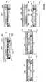
도 1a는 접착된 계면에서의 n--도핑된 판독 웨이퍼와 p--도핑된 흡수체 웨이퍼 사이의 p-n 접합이 있는 본 발명의 모놀리식 화소 검출기의 단면도.
도 1b는 p--도핑된 흡수체 웨이퍼에 접착되는 n--도핑된 판독 웨이퍼 안쪽에 p-n 접합이 있는 본 발명의 모놀리식 화소 검출기의 단면도.
도 1c는 접착된 계면에서 p--도핑된 판독 웨이퍼와 n--도핑된 흡수체 웨이퍼 사이의 p-n 접합이 있는 본 발명의 모놀리식 화소 검출기의 단면도.
도 2a는 판독 및 흡수체 웨이퍼에서의 n+-도핑된 영역들 사이의 공유 반도체 본드들과 화소 격리를 위한 산화물-대-산화물 본드들을 통한 전하 수집이 있는 본 발명의 모놀리식 화소 검출기의 단면도.
도 2b는 판독 및 흡수체 웨이퍼에서의 n+-도핑된 영역들 사이의 공유 반도체 본드들과 화소 분리를 위한 비전도성 본드들을 통한 전하 수집이 있는 본 발명의 모놀리식 화소 검출기의 단면도.
도 2c는 판독 및 흡수체 웨이퍼에서의 n+-도핑된 영역들 사이의 공유 반도체 본드들과 화소 분리를 위한 흡수체 웨이퍼 및 판독 웨이퍼의 산화물 영역들 사이의 비전도성 본드들을 통한 전하 수집이 있는 본 발명의 모놀리식 화소 검출기의 단면도.
도 2d는 판독 및 흡수체 웨이퍼에서의 n+-도핑된 영역들 사이의 공유 반도체 본드들, 공유 p--n+ 본드들 및 화소 분리를 위한 트렌치 격리를 통한 전하 수집이 있는 본 발명의 모놀리식 화소 검출기의 단면도.
도 2e는 흡수체 웨이퍼가 전하 증배를 위한 영역을 포함하고, 흡수체 웨이퍼에서의 n+-도핑된 영역들과 판독 웨이퍼의 고저항성 영역들 사이의 비전도성 본드들과 판독 및 흡수에 웨이퍼에서의 n+-도핑된 영역들 사이의 공유 반도체 본드들을 통한 전하 수집이 있는 본 발명의 모놀리식 화소 검출기의 단면도.
도 2f는 실리콘 웨이퍼의 전하 증배 영역과 판독 웨이퍼에서의 n+-도핑된 영역들 사이의 제1 공유 반도체 본드와, 실리콘 웨이퍼와 흡수체 웨이퍼 사이의 제2 공유 반도체 본드를 통한 전하 수집이 있는 본 발명의 모놀리식 화소 검출기의 단면도.
도 2g는 판독 웨이퍼의 약하게 p-도핑된 영역들과 흡수체 웨이퍼의 p+-도핑된 영역들 사이의 공유 반도체 본드들, 흡수체 웨이퍼의 고저항성 영역들과 판독 웨이퍼의 약하게 p-도핑된 영역 사이의 비전도성 본드들을 통한 전하 수집이 있는 본 발명의 모놀리식 화소 검출기의 단면도로서, 그러한 흡수체 웨이퍼는 전하 증배를 위한 영역을 포함하는, 단면도.
도 3a는 본 발명의 모놀리식 화소 검출기의 전하 컬렉터들의 평면도.
도 3b는 본 발명의 모놀리식 화소 검출기의 화소들을 둘러싸는 산화물 영역들과 전하 컬렉터들의 평면도.
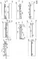
도 4는 많이 도핑된 전하 컬렉터 플러그들이 있는, 본 발명의 얇은 판독 웨이퍼의 제작을 위한 본 발명의 공정 흐름을 도시하는 도면.
도 5는 많이 도핑된 전하 컬렉터 플러그들과 임플란트들이 있는, 본 발명의 얇은 판독 웨이퍼의 제작을 위한 본 발명의 공정 흐름을 도시하는 도면.
도 6은 금속 전하 컬렉터 플러그들과 금속 층들이 있는, 본 발명의 얇은 판독 웨이퍼의 제작을 위한 본 발명의 공정 흐름을 도시하는 도면.
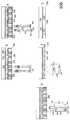
도 7a는 임플란트들과, 화소 격리를 위한 산화물 영역들을 포함하는 본 발명의 흡수체 웨이퍼의 제작을 위한 본 발명의 공정 흐름을 도시하는 도면.
도 7b는 화소 격리를 위한 산화물 영역들과 함께 금속 영역들을 포함하는 본 발명의 흡수체 웨이퍼의 제작을 위한 본 발명의 공정 흐름을 도시하는 도면.
도 7c는 본 발명의 패턴화되지 않은 흡수체 웨이퍼의 제작을 위한 본 발명의 공정 흐름을 도시하는 도면.
도 8은 많이 도핑된 캡(cap)들이 있는 에피텍셜 필러(pillar)들을 포함하는 본 발명의 흡수체 웨이퍼의 제작을 위한 본 발명의 공정 흐름을 도시하는 도면.
도 9는 많이 도핑된 캡들, 에피층 및 화소 격리를 위한 산화물 영역들이 있는 에피텍셜 필러들을 포함하는 본 발명의 흡수체 웨이퍼의 제작을 위한 본 발명의 공정 흐름을 도시하는 도면.
도 10은 많이 도핑된 캡들, 금속 층 및 화소 격리를 위한 산화물 영역들이 있는 에피텍셜 필러들을 포함하는 흡수체 웨이퍼의 제작을 위한 본 발명의 일 변형예의 공정 흐름을 도시하는 도면.
도 11은 에피텍셜 재료로 채워진 정공(hole)들이 있는 본 발명의 흡수체 웨이퍼의 제작을 위한 본 발명의 공정 흐름을 도시하는 도면.
도 12a는 접착된 흡수체 웨이퍼가 있는 본 발명의 검출기 구조의 제작을 위한 본 발명의 공정 흐름을 도시하는 도면.
도 12b는 접착된 패턴화되지 않은 흡수체 웨이퍼가 있는 본 발명의 검출기 구조의 제작을 위한 본 발명의 공정 흐름을 도시하는 도면.
도 12c는 에피텍셜 재료로 채워진 정공들을 포함하는 접착된 흡수체 웨이퍼가 있는 본 발명의 검출기 구조의 제작을 위한 본 발명의 공정 흐름을 도시하는 도면.
도 13은 얇은 판독 웨이퍼의 많이 도핑된 영역들에 접착된 에피텍셜 필러들이 있는 본 발명의 검출기 구조를 도시하는 도면.
도 14는 많이 도핑된 영역들이 있는 얇은 판독 웨이퍼에 접착된 에피텍셜 필러들 상의 많이 도핑된 영역들이 있는 본 발명의 검출기 구조를 도시하는 도면.
도 15는 얇은 판독 웨이퍼 상의 금속 영역들에 접착된 금속화된 에피텍셜 필러 영역들이 있는 본 발명의 검출기 구조를 도시하는 도면.
도 16은 얇은 판독 웨이퍼에 접착되는 얇은 기판 상에 에피텍셜 필러들을 포함하는 본 발명의 검출기 구조를 도시하는 도면.Figure 1a is a n at the bondinterface-sectional view of the monolithic type pixel detectors of the present invention with a pn junction between doped waferabsorber-doped wafer with p read -.
Figure 1b is ap-n that are attached to the absorption body dopedwafer-monolithic cross-sectional view of the pixel detector of the present invention with a pn junction to the inside of the read-doped wafer.
Figure 1c p in the bondinginterface-sectional view of a monolithic pixel detector of the present invention with a pn junction between doped waferabsorber-doped wafer and the read n -.
2A is a cross-sectional view of a monolithic pixel detector of the present invention with charge collection through shared semiconductor bonds between n+ -doped regions in the read and absorber wafer and oxide-to-oxide bonds for pixel isolation.
2B is a cross-sectional view of a monolithic pixel detector of the present invention with charge collection through shared semiconductor bonds between n+ -doped regions in the read and absorber wafer and non-conductive bonds for pixel separation.
Figure 2c is a view of the present invention with charge collection via shared semiconductor bonds between n+ -doped regions in the read and absorber wafer and non-conductive bonds between the oxide regions of the read wafer and the absorber wafer for pixel separation. A cross-sectional view of a monolithic pixel detector.
Figure 2d is a monolithic representation of the invention with shared semiconductor bonds between n+ -doped regions in the read and absorber wafer, shared p-- n+ bonds and charge collection through trench isolation for pixel separation. A cross-sectional view of a pixel detector.
2E shows that the absorber wafer includes a region for charge multiplication, and the non-conductive bonds between the n+ -doped regions in the absorber wafer and the high resistivity regions of the read wafer and n+ in the wafer to read and absorb. -A cross-sectional view of a monolithic pixel detector of the invention with charge collection through shared semiconductor bonds between doped regions.
Figure 2f shows the present invention with charge collection via a first shared semiconductor bond between the charge multiplication region of the silicon wafer and the n+ -doped regions of the read wafer and the second shared semiconductor bond between the silicon wafer and the absorber wafer. A cross-sectional view of a monolithic pixel detector.
2G shows shared semiconductor bonds between the weakly p-doped regions of the read wafer and the p+ -doped regions of the absorber wafer, between the highly resistive regions of the absorber wafer and the weakly p-doped regions of the read wafer. A cross-sectional view of a monolithic pixel detector of the present invention with charge collection through non-conductive bonds, such an absorber wafer comprising a region for charge multiplication.
3A is a plan view of charge collectors of a monolithic pixel detector of the present invention.
3B is a plan view of oxide regions and charge collectors surrounding pixels of the monolithic pixel detector of the present invention.
Figure 4 shows the inventive process flow for fabrication of the inventive thin read wafer, with heavily doped charge collector plugs.
5 shows the inventive process flow for fabrication of the inventive thin read wafer, with heavily doped charge collector plugs and implants.
6 shows the inventive process flow for the fabrication of the inventive thin read wafer, with metal charge collector plugs and metal layers.
7A is a diagram showing a process flow of the present invention for fabrication of an absorber wafer of the present invention including implants and oxide regions for pixel isolation.
7B is a diagram showing a process flow of the present invention for fabricating an absorber wafer of the present invention including metal regions together with oxide regions for pixel isolation.
7C is a diagram showing the process flow of the present invention for fabrication of an unpatterned absorber wafer of the present invention.
8 is a diagram showing the inventive process flow for the fabrication of an inventive absorber wafer comprising epitaxial pillars with heavily doped caps.
9 shows a process flow of the present invention for fabrication of an absorber wafer of the present invention including highly doped caps, an epitaxial layer and epitaxial fillers with oxide regions for pixel isolation.
10 is a diagram illustrating a process flow of a variant of the present invention for fabrication of an absorber wafer including epitaxial fillers with heavily doped caps, a metal layer and oxide regions for pixel isolation.
11 is a diagram showing the inventive process flow for the fabrication of the inventive absorber wafer with holes filled with epitaxial material.
12A shows the inventive process flow for fabrication of the inventive detector structure with an adhered absorber wafer.
Fig. 12B shows the inventive process flow for fabrication of the inventive detector structure with an adhered unpatterned absorber wafer.
12C shows the inventive process flow for the fabrication of the inventive detector structure with an adhered absorber wafer comprising holes filled with an epitaxial material.
13 shows a detector structure of the present invention with epitaxial fillers adhered to heavily doped regions of a thin readout wafer.
Fig. 14 shows a detector structure of the present invention with heavily doped regions on epitaxial fillers adhered to a thin readout wafer with heavily doped regions.
Fig. 15 shows a detector structure of the present invention with metallized epitaxial filler regions bonded to metal regions on a thin readout wafer.
Fig. 16 shows a detector structure of the present invention including epitaxial fillers on a thin substrate adhered to a thin readout wafer.
본 발명의 목적은 전자파 복사를 검출하기 위한 민감한 화소 검출기(예: 최대 20×20㎠ 또는 최대 약 40×40㎠의 크기를 갖는 평면 패널 X선 검출기 및 적외선 검출용 고해상도 검출기)의 제작을 위한 간단한 구조와 방법을 제공하는 것이다. 검출기는 얇은 CMOS 웨이퍼에서 처리된 판독 유닛으로 구성되며, 이 유닛의 뒷면은 센서 웨이퍼라고도 불리는 흡수체 웨이퍼에 접합된다. 이러한 검출기는 모두 후방 조사를 위해 구성되며, 여기서 전자기 방사선이 CMOS 스택의 반대쪽에서 흡수체에 입사한다. 본딩은 웨이퍼 스케일 상에서 이루어지며, 적어도 전하 수집을 위한 본딩은 예를 들면 많이 도핑된 반도체들 사이의 공유 반도체 본드들과 같이 판독 웨이퍼와 흡수체 웨이퍼의 전기적으로 전도성이 높은 영역들 사이에 만들어진다. 예를 들어, 판독 전자기기는 두께가 약 10㎛ 내지 30㎛이거나 바람직하게는 5㎛ 내지 10㎛이거나 심지어 3㎛ 내지 5㎛이고, 저항률은 약 500Ω㎝ 위 또는 바람직하게는 약 1㏀cm 내지 2㏀cm 이상 또는 더 바람직하게는 2㏀cm 내지 5㏀cm 이상일 때 또는 심지어 예를 들면 5㏀cm 내지 50㏀cm과 같이 5㏀cm 위인 에피텍셜 Si 층에서 처리되고, 그러한 저항률은 제1 전도 유형(예를 들면, p-도핑에 의해 유도된 p-전도)의 약 1011㎝-3 내지 1013㎝-3 사이에 있는 낮은 도핑 수준으로 인한 것이다. 검출기 제조의 용이성을 위해, 판독 전자기기의 CMOS 처리에 SOI(silicon-on-inslator) 웨이퍼들을 사용하는 것이 유리할 수 있다. 검출기들은 단일 광자 검출 모드에서 전자기 방사선을 검출할 수 있다. 센서 재료는 고순도 웨이퍼의 형태 또는 기판에서 성장한 에피텍셜 층들의 형태로 사용 가능한 모든 반도체를 포함할 수 있으며, 기판에는 예를 들어 Si, Ge, GaA, CdTe, CdZnTe 합금 또는 InSb가 포함될 수 있으며, 이들은 검출기 제작시 선택적으로 제거될 수 있다. 센서에 사용되는 두께와 재료는 검출될 전자기 방사선의 에너지에 따라 크게 달라진다. 적외선에서부터 가시광선, 자외선 및 소프트 X선에 이르는 스펙트럼 범위를 포함하는 수 keV까지의 eV의 약 10분의 1로부터의 낮은 에너지 방사선을 검출하는 경우, ㎛ 이하의 크기의 두께로 충분할 수 있다. 예를 들어 밴드 갭이 증가하는 순서대로 HgCdTe 합금, InSb, InGaAs 합금, Ge, Si, SiGe 합금, InP, GaAs, InGaN 합금, GaN, C(다이아몬드)와 같은 이러한 에너지 범위를 포함하는 많은 Ⅱ/Ⅵ, Ⅲ/V 및 그룹 IV 반도체들이 존재한다. 일 예로서, 근적외선 검출의 경우 0.5㎛ 내지 1.5㎛만큼 또는 심지어 0.3㎛ 내지 0.5㎛만큼 얇은 Ge 층으로도 효율적인 감지를 위해 충분할 수 있다. 따라서 웨이퍼 본딩은, 예를 들면 수소 이식 및 박리와 같이 웨이퍼를 얇게 하는 것과 결합되어야 할 수 있다(예를 들면, 본 명세서에 전문이 참조로 통합되어 있고, I.P.Ferain 등에 의한 J. Appl. 107, 054315(2010)를 참조하라). 적외선 검출기들의 감도는 흡수체 웨이퍼의 흡수 영역과 통신하는 애벌랜치 전하 증배(charge multiplication) 영역을 통합함으로써 더욱 향상될 수 있다.An object of the present invention is a simple method for fabricating a sensitive pixel detector for detecting electromagnetic radiation (eg, a flat panel X-ray detector having a size of up to 20×20 cm2 or a maximum of about 40×40 cm2 and a high-resolution detector for infrared detection). It is to provide structure and method. The detector consists of a read unit processed on a thin CMOS wafer, the back side of which is bonded to an absorber wafer, also called a sensor wafer. Both of these detectors are configured for back-illumination, where electromagnetic radiation is incident on the absorber on the opposite side of the CMOS stack. The bonding is done on the wafer scale, at least the bonding for charge collection is made between the electrically conductive regions of the read wafer and the absorber wafer, for example shared semiconductor bonds between heavily doped semiconductors. For example, the reading electronics have a thickness of about 10 μm to 30 μm, preferably 5 μm to 10 μm, or even 3 μm to 5 μm, and the resistivity is about 500 Ωcm above or preferably about 1 kΩcm to 2 μm. It is treated in a layer of epitaxial Si that is 5kcm or more, or more preferably 2kcm to 5kcm or more, or even 5kcm above, such as for example 5kcm to 50kcm, and such resistivity is the first conduction type This is due to the low doping level between about 1011 cm-3 and 1013 cm-3 of (eg, p-conduction induced by p-doping). For ease of detector fabrication, it may be advantageous to use silicon-on-inslator (SOI) wafers for CMOS processing of readout electronics. The detectors are capable of detecting electromagnetic radiation in a single photon detection mode. The sensor material may include all semiconductors available in the form of high purity wafers or epitaxial layers grown on the substrate, and the substrate may include, for example, Si, Ge, GaA, CdTe, CdZnTe alloy or InSb, and these It can be selectively removed when making the detector. The thickness and material used in the sensor depend greatly on the energy of the electromagnetic radiation to be detected. When detecting low energy radiation from about a tenth of the eV up to several keVs covering the spectral range from infrared to visible, ultraviolet and soft X-rays, a thickness of a size of µm or less may be sufficient. Many II/VI cover these energy ranges, for example HgCdTe alloys, InSb, InGaAs alloys, Ge, Si, SiGe alloys, InP, GaAs, InGaN alloys, GaN, C (diamonds) in the order of increasing band gap. , III/V and Group IV semiconductors exist. As an example, in the case of near-infrared detection, a Ge layer as thin as 0.5 μm to 1.5 μm or even 0.3 μm to 0.5 μm may be sufficient for efficient detection. Thus, wafer bonding may have to be combined with thinning of the wafer, for example hydrogen implantation and exfoliation (e.g., J. Appl. 107, 054315 by IPFerain et al., incorporated herein by reference in its entirety, and (2010)). The sensitivity of the infrared detectors can be further improved by incorporating an avalanche charge multiplication region that communicates with the absorption region of the absorber wafer.
예를 들면 소프트 X선과 하드 X선 검출 사이의 영역에서는, 두께가 약 3.5㎛, 332㎛ 및 2310㎛인 SiC 센서가 각각 2keV, 10keV 및 20keV의 에너지로 입사 광자들의 90%를 흡수할 수 있다. 두께가 약 3.9㎛, 334㎛ 및 2330㎛인 Si 센서는 각각 2keV, 10keV 및 20keV의 에너지로 입사 광자들의 90%를 흡수할 수 있다. Ge 또는 GaAs 센서의 경우, 20keV, 30keV, 40keV의 에너지로 입사 광자들의 90%를 흡수하는 데 필요한 두께는 각각 약 105㎛, 320㎛ 및 710㎛이다. 예를 들어, Si0.2Ge0.8 합금은 이러한 광자 에너지에서 동일한 흡수를 위해 약 25% 더 두꺼워야 한다. 두께가 약 210㎛, 610㎛, 1310㎛인 CdTe 센서 또는 CdZnTe 합금 센서에 의해 40keV, 60keV, 80keV의 더 단단한 X선들이 동일한 정도로 흡수된다(NIST X선 감쇠 데이터 베이스,nist.gov/pml/data/ffasf). 고유한(intrinsic) Ge의 실온 저항은 약 47Ω㎝이며, Si0.25Ge0.75 합금의 실온 저항은 약 6×10⁴Ω㎝이다(예를 들면virginiasemi.com/pdf/generalpropertiesSi62002.pdf를 참조하라). 따라서 Ge 또는 SiGe 흡수체들을 포함하는 X선 검출기들은 다크(dark) 누설 전류들을 예를 들면 화소 당 1㎁ 또는 심지어 10㎀와 100㎀ 사이의 허용 가능한 수준으로 낮추기 위해 냉각될 필요가 있다. Ge 및 SiGe 센서들에 관해서, GaAs 센서들은 109Ω㎝의 순서로 훨씬 더 높은 저항성을 가진다(예를 들면, 본 명세서에 전문이 참조로 통합되어 있고 M.C. Veale에 의한 in Nucl Instr. Meth. Phys. Res, A 752, 6(2014)를 참조하라). 동일한 크기의 저항률이 CdTe 센서에 적용되며, 심지어 CdZnTe 합금 센서들에 대해서는 더 높은 것이 적용된다(예를 들면, 본 명세서에 전문이 참조로 통합되어 있고 S. Del Sordo 등에 의한, in Sensors 2009, 9, 3491-3526을 참조하라)For example, in the region between soft X-ray and hard X-ray detection, SiC sensors with thicknesses of about 3.5 µm, 332 µm, and 2310 µm can absorb 90% of incident photons with energies of 2 keV, 10 keV and 20 keV, respectively. Si sensors with thicknesses of about 3.9 μm, 334 μm, and 2330 μm can absorb 90% of incident photons with energy of 2 keV, 10 keV and 20 keV, respectively. For Ge or GaAs sensors, the thicknesses required to absorb 90% of incident photons with energies of 20 keV, 30 keV and 40 keV are about 105 μm, 320 μm and 710 μm, respectively. For example, Si0.2 Ge0.8 alloy should be about 25% thicker for the same absorption at this photon energy. Harder X-rays of 40 keV, 60 keV and 80 keV are absorbed to the same extent by a CdTe sensor or CdZnTe alloy sensor of about 210 μm, 610 μm, and 1310 μm in thickness (NIST X-ray attenuation database,nist.gov/pml/data). /ffasf ). Room temperature resistance of the inherent (intrinsic) Ge is about 47Ω㎝, room temperature resistance of the Si0.25 Ge0.75 alloy is about 6 × 10⁴ Ω㎝ (Be e.g. seevirginiasemi.com/pdf/generalpropertiesSi62002.pdf). Therefore, X-ray detectors comprising Ge or SiGe absorbers need to be cooled to lower the dark leakage currents to an acceptable level, for example between 1 µA per pixel or even between 10 µA and 100 µA. With regard to Ge and SiGe sensors, GaAs sensors have a much higher resistivity in the order of 109 Ωcm (e.g., in Nucl Instr. Meth. Phys by MC Veale, incorporated herein by reference in its entirety and by MC Veale) See Res, A 752, 6 (2014)). The same size resistivity applies to CdTe sensors, even higher for CdZnTe alloy sensors (eg, in
본 발명의 구조들과 방법들은 산업용 웨이퍼들을 지칭한다. 200mm 웨이퍼용 고진공 본딩 장비는 예를 들면 EV 그룹이 제작한다(예를 들면, 본 명세서에 전문이 참조로 통합되어 있고 C. Flotgen 등에 의한 in ECS Transactions 64, 103(2014)을 참조하라).The structures and methods of the present invention refer to industrial wafers. High vacuum bonding equipment for 200mm wafers is made by the EV group, for example (see, for example, in ECS Transactions 64, 103 (2014) by C. Flotgen et al., incorporated herein by reference in its entirety).
구성에 의해, 본 발명의 단층 화소 검출기는 단일 광자 검출기를 제공할 것으로 예상된다. 따라서 본 발명의 단일 X선 화소 검출기는 에너지 차이(discrimination)에 적합하며, 여기서 흡수체에 발생하는 광자의 에너지는 판독 전자기기로 처리되는 전기 펄스들의 높이를 분석하여 측정될 수 있다.By construction, it is expected that the tomographic pixel detector of the present invention will provide a single photon detector. Therefore, the single X-ray pixel detector of the present invention is suitable for energy discrimination, where the energy of photons generated in the absorber can be measured by analyzing the height of the electric pulses processed by the readout electronics.
종래 기술의 접근법들(예를 들면, 본 명세서에 전문이 참조로 통합되어 있고 von Kanel에 의한 국제 특허출원 WO2016/097850호 및 von Kanel에 대한 국제 특허출원 PCT/IB2017/001032호를 참조하라)과는 대조적으로, 본 발명에서는 전하 캐리어들이 판독 전자기기들과 통신하는 전하 컬렉터들에 도달하기 전에 가볍게 도핑된 재료들 사이의 접착 계면과 교차하지 않는다. 대신 전하들은 소수 캐리어 생성과 재결합이 일어나지 않는 고전도성 영역들 사이의 접착 계면들을 통해 흘러 들어간다(channelled). 모든 다음 실시예들에서, 화소 검출기들은 배면 조사를 위해 구성되고, 이 경우 전자기 복사선은 반대 측 상에 CMOS 스택이 있는 얇은 실리콘 CMOS 기판의 배면 상에 접착된 흡수체 상에 입사된다.Prior art approaches (see, for example, international patent application WO2016/097850 by von Kanel and international patent application PCT/IB2017/001032 to von Kanel, which is incorporated herein by reference in its entirety) and In contrast, in the present invention the charge carriers do not intersect the adhesive interface between the lightly doped materials before reaching the charge collectors communicating with the readout electronics. Instead, charges channeled through the bonding interfaces between the highly conductive regions where minority carrier generation and recombination do not occur. In all the following embodiments, the pixel detectors are configured for backside irradiation, in which case electromagnetic radiation is incident on an absorber adhered on the backside of a thin silicon CMOS substrate with a CMOS stack on the opposite side.
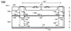
이제 도 2a를 참조하면, X선들을 탐지하도록 된 모놀리식 화소 검출기(101)의 제1 전형적인 실시예(100)는 두께가 d1인 얇은 판독 웨이퍼(102)와 두께가 d2인 흡수체 웨이퍼(104) 사이의 접착 계면을 포함한다. 이러한 판독 웨이퍼는, 예를 들면 모든 처리가 완료된 후, 약 10㎛ 내지 30㎛ 또는 바람직하게는 약 5㎛ 내지 10㎛ 또는 심지어 3㎛ 내지 5㎛까지 얇아지는 바람직하게는 약 1㏀㎝ 내지 2㏀㎝ 또는 심지어 2㏀㎝ 내지 5㏀㎝의 저항률을 갖는 약하게 p-도핑된 기판(106)을 CMOS 처리함으로써 바람직하게 제작된다. 얇게 하는 것은 CMOS 스택의 평탄화를 요구하고, 기판(106) 전의 캐리어 웨이퍼의 본딩은 얇아질 수 있다. 접착 계면은 실리콘 관통 비아(silicon-through-via)(110)들을 닮은 구조물들 사이의 전도성의 공유 반도체 본드(108)로 구성되지만, 약하게 p-도핑된 기판(106)과 n+-p 접합을 형성하는 고도로 전도성 n+-도핑된 반도체 물질로 채워져 있다. 다음에서, 기판(106)을 통해 확장되는 이들 n+-도핑된 비아(via)들은 단순히 플러그(plug)(110)들이라고 불릴 것이다. 예를 들어, 도핑이 많이 되는 임플란트들일 수 있는 저항성이 높은 p-전도성 흡수체 웨이퍼(104)에서 플러그(110)들은 전도성이 높은 n+-도핑된 영역(112)를 가진 옴 접점(ohmic contact)을 형성한다. 예를 들어, 전도성이 높은 플러그(110)의 도핑 수준은 1×1018cm-3와 1×1019cm-3 사이 또는 바람직하게는 1×1019cm-3와 1×1020cm-3사이 또는 심지어 1×1020cm-3와 5×1020cm-3 사이에 있을 수 있고, 이는 각각 약 5mΩ㎝ 내지 20mΩ㎝, 0.7mΩ㎝ 내지 5mΩ㎝ 및 0.2mΩ㎝ 내지 0.7mΩ㎝ 사이의 저항률에 해당한다. 고 전도성 영역(112)들은 유사한 도핑 수준들을 가질 수 있다. 예를 들어 가볍게 p 도핑된 기판(106)에서의 에칭 구멍들과 관련 분야에서 알려진 이어지는 에피텍시 단계에서의 n+-재료를 채우는 것에 의해 많이 도핑된 플러그(110)들이 형성될 수 있다. 실시예(100)의 또 다른 양태에서는 임플란트(112)들 대신 유사한 에피텍시 공정으로 인해 많이 도핑된 컬럼(124)들이 대부분의 또는 모든 흡수체 웨이퍼(104)를 통해 확장되는 유사한 수준까지 도핑될 수 있다. 선택적으로, 흡수체 웨이퍼(104)는 금속 역 접점(116)으로 옴 접촉 형성을 용이하게 하는 많이 p-도핑된 층(117)을 더 포함할 수 있다. 많이 도핑된 임플란트들(112) 또는 컬럼(124)들에 접착된 많인 도핑된 플러그(110)들은 전하 컬렉터로서 역할을 하며, 흡수체 웨이퍼(104)에서 입사하는 전자기 방사선에 의해 발생되고, 흡수체 웨이퍼(104) 상의 역 접촉(116)에 전압을 인가시 n+-도핑된 영역들(112, 124)과 고전도성의 p-전도 흡수체 웨이퍼(104)에 의해 형성된 역바이어스된 p-n 접합(114, 126)의 전기장에서 분리되는 전자-정공 쌍들로부터 전자들을 수집한다. 따라서 소수 캐리어(전자들)는 트래핑(trapping)과 재결합이 발생할 수 있는 낮게-도핑된 웨이퍼들 사이의 접착 계면을 가로질러 결코 이동하지 않는다. 전하 컬렉터(110)들은 판독 웨이퍼(102)의 화소 판독 전자기기(115)와 통신하며, 여기서 전자기 방사선에 의해 발생하는 전하 펄스들은 처리되어 판독 전자기기의 오프-화소(off-pixel) 부분으로 전달된다. 검출기 화소들은 도핑이 많이 이루어진 플러그/영역들(110/112, 110/124), 폭(118, 119, 128)에 의해 규정되며, 이러한 폭의 범위는 예를 들어 약 0.5㎛ 내지 2.5㎛ 또는 바람직하게는 약 1㎛ 내지 1.5㎛인 범위를 가질 수 있다. 판독 웨이퍼(102)에서의 많이 도핑된 플러그(110)들의 폭(118)과 흡수체 웨이퍼(104)에서의 많이 도핑된 영역들(112, 124)의 폭(119, 128)은 같을 필요는 없지만 바람직하게는 그것들 중 적어도 하나는 본딩을 위해 웨이퍼들(102, 104)의 정확한 정렬을 촉진하기 위해 적어도 1㎛ 내지 1.5㎛의 범위에 있어야 한다. 정확한 정렬을 허용하기 위해 얇은 판독 웨이퍼(102)와 흡수체 웨이퍼(104)는 모두, 예를 들면 반대 측들에서 웨이퍼 가장자리에 가깝게 위치하는 정렬 마크들의 형태로 된 적어도 2개의 특수한 웨이퍼 정렬 특징들을 구비한다. 그러한 정렬 마크들의 중첩을 통해 200mm 웨이퍼들의 회전 오정렬은 약 (2 - 5)×10-4° 내에서, 측면 오정렬은 약 0.5㎛ 내지 1㎛ 내로 유지될 수 있다. 웨이퍼 본딩이 작은 경우에도 유사한 정확도를 얻을 수 있다. 예를 들어 EVGroup은 정확도가 1 ㎛ 미만인 정렬 도구를 제공한다(예를 들면, 본 명세서에 전문이 참조로 통합되어 있는evgroup.com/en/products/bonding/integrated bonding/evg combond를 참조하라). 영역들(112/124)과 접촉하는 도핑된 플러그들(110) 사이의 거리(L)는 약 100㎛ 내지 200㎛, 50㎛ 내지 100㎛ 또는 20㎛ 내지 50㎛ 또는 심지어 5㎛ 내지 20㎛ 내의 넓은 범위에서 변할 수 있는 화소 크기(113)를 규정한다. 도핑된 컬럼(124)들을 임플란트들(112) 대신 사용하는 것은 화소 크기가 흡수체 두께(d2) 보다 작을 때 역접점(116)에 인가된 더 낮은 전압들에서 흡수체(104)의 더 쉬운 디플리션이라는 장점을 가진다. 흡수체 웨이퍼(104)에서의 많이 도핑된 임플란트들(112)은 고저항성 영역들(120)에 의해 둘러싸이고 그 저항률은 적어도 104 내지 106인 인자만큼 임플란트들(112)의 저항률보다 높다. 영역들(120)은 심지어 산화물 영역들과 같은 절연 영역들일 수 있고, 판독 웨이퍼와 흡수체 웨이퍼 사이의 있는, 전도성이 빈약하거나 전기적으로 절연성인 산화물-대-산화물 또는 산화물-대-산화물 본드(122)를 형성할 수 있으며, 그 저항률은 본드(108)의 저항률보다 적어도 103 내지 104또는 바람직하게는 104 내지 106, 또는 더 바람직하게는 106 내지 108인 인자만큼 더 높다. 따라서 이들 고저항성 영역들은 2개의 웨이퍼들 사이의 전기적 접속만이 많이 도핑된 영역들(110)과 영역들(112, 124) 사이에서 만들어지도록 낮게 도핑된 고저항성의 흡수체 웨이퍼(104)로부터 판독 웨이퍼(102)(즉, 기판(106))의 낮게 도핑된 영역들을 절연시킨다. 동시에 영역들(120)은 인접하는 화소들을 서로 절연시킨다.Referring now to Figure 2a, a first
실시예(100)에 따른 화소 검출기는 흡수체 웨이퍼(104)에서 X선들에 의해 생성된 전자-정공 쌍들로부터 전자들을 검출하기 위해 설계된다. 이러한 실시예의 일 양태에서, 검출기는 도핑 부호(sign)들을 반대로 함으로써 정공 수집을 위해 설계될 수 있다. p-도핑된 영역들의 도핑 수준들은 위에서 논의된 n-도핑된 영역들의 도핑 수준들과 거의 같다. 약 1.5인 인자만큼 다소 더 높은 도핑이 n-도핑 경우에 대한 유사한 저항률 수준들에 대해 필요하다.The pixel detector according to
도 2a에 따르면, 실시예(100)는 많이 도핑된 플러그들(110)과 많이 도핑된 영역들(112, 124) 사이에 전기적 접촉을 형성하기 위해, 판독 웨이퍼(102)와 흡수체 웨이퍼(104)의 정밀한 상호 정렬을 필요로 한다.According to Fig. 2A,
이제 도 2b를 참조하면, X선들을 탐지하도록 된 모놀리식 화소 검출기(101')의 제2 실시예(100')는 두께가 d1'인 얇은 판독 웨이퍼(102')와 두께가 d2'인 흡수체 웨이퍼(104') 사이의 접착 계면을 포함할 수 있다. 예를 들면, 판독 웨이퍼는 두께 d1'가 약 10㎛ 내지 30㎛ 또는 바람직하게는 약 5㎛ 내지 10㎛ 또는 심지어 3㎛ 내지 5㎛이고 저항률이 약 1㏀cm 내지 2㏀cm 또는 2㏀cm 내지 5㏀cm인 약하게 p-도핑된 기판을 CMOS가 처리에 의해 제작되었을 수 있으며, 이러한 두께까지 얇게 하는 것은 CMOS 스택의 평탄화와 캐리어 웨이퍼를 기판(106')에 접착시키는 것을 요구할 수 있다. 판독 웨이퍼(102')는 고전도성의 n+-도핑된 플러그들(110')를 포함할 수 있으며, 이 플러그는 고도로 도핑된 영역들(110', 112')보다 최소 104 내지 106 높은 저항률을 갖는, 고저항성 또는 절연성 영역(120')으로 둘러싸인 기판(106')을 통해 확장될 수 있다. 예를 들어 고저항 영역(120')은 고저항 p-전도성 흡수체 웨이퍼(104')에 접합되기 전에 웨이퍼(102')의 국부적 비정질화 또는 국부적 산화에 의해 형성되었을 수 있다. 대안적으로, 약 2㏀cm 위인 판독 웨이퍼(102')의 저항률에 대해서는, 고저항 영역(120')을 특별히 형성할 필요가 없을 수 있다. 예를 들어 전도성이 높은 플러그들(110')의 도핑 수준은, 약 5mΩ㎝ 내지 20mΩ㎝, 0.7mΩ㎝ 내지 5mΩ㎝ 및 0.2mΩ㎝ 내지 0.7mΩ㎝ 사이의 저항률에 대응하는 1×1018cm-3와 1×1019cm-3사이 또는 바람직하게 1×1019cm-3와 1×1020cm-3사이 또는 심지어 1×1020cm-3와 5×1020cm-3사이일 수 있다. 예를 들어, 가볍게 p-도핑된 기판(106')에서 에칭 구멍들에 의해 무겁게 도핑된 플러그들(110')을 제작할 수 있으며, 그러한 구멍들을 이어지는 에피텍시 단계에서 n+-재료로 채우는 것은 관련 분야에서 알려져 있다. 흡수체 웨이퍼(104')는 예를 들면, 플러그들(110')과 유사한 도핑 형태와 도핑 수준을 가질 수 있는 이온 이식에 의해 형성된 무겁게 도핑되고 고전도성이며 비정형(unstructured) 표면층(112')을 바람직하게 포함한다. 선택적으로, 흡수체 웨이퍼(104')는 무겁게 p-도핑된 층(117')을 더 포함할 수 있어서, 금속 뒤 접점(116')으로 옴 접촉 형성을 용이하게 한다. 무겁게 도핑된 플러그(110')는 흡수체 웨이퍼(104')의 무겁게 도핑된 표면 영역들(112')과 옴 접촉들을 형성한다. 한편, 전도성 표면층(112')은 흡수체 웨이퍼(104')의 고저항성 p-전도성 벌크 영역이 있는 p-n 접합(114')을 형성한다. 상기 옴 접촉들을 제공하는 전도성 공유 반도체 본드들(108')에 의해 무겁게 도핑된 영역들(112')에 접합된 무겁게 도핑된 플러그들(110')은 전하 컬렉터들의 역할을 하고 흡수체 웨이퍼(104')에 입사하는 전자기 방사선에 의해 생성되고 전압을 흡수체 웨이퍼(104') 상의 뒤 접점(116')에 인가시 흡수체 웨이퍼(104')의 무겁게 n-도핑된 표면 영역(112')과 p-전도성 벌크 영역에 의해 형성된 역 바이어스된 p-n 접합(114')의 전기장에서 분리되는 전자-정공 쌍들로부터 전자들을 수집한다. 하지만 전자들은 사실상 판독 웨이퍼(102')의 고저항성 영역들(120')과 흡수체 웨이퍼(104')의 도핑된 영역들(112') 사이의 전도성이 빈약한 접착 계면(122')과 교차하지 않는데, 이는 그것의 저항이 적어도 103 내지 104, 또는 바람직하게는 104 내지 106, 또는 심지어 더 바람직하게는 106 내지 108인 인자만큼 전도성 본드들의 저항을 초과하기 때문이다. 그러므로 소수 캐리어들(전자들)은 트래핑과 재결합이 발생할 수 있는 낮게 도핑된 웨이퍼들 사이의 접착 계면을 가로질러 절대 움직이지 않는다. 따라서 영역들(120')에는 화소 격리가 생기고 화소 판독 전자기기(115')에 있는 p-MOS 트랜지스터들의 n-웰(well)들이 흡수체 웨이퍼(104')에서 전자기 방사선에 의해 생성된 전자들을 안독으로 집는 n-도핑 플러그들(110')와 함께 전하 컬렉터들의 역할을 하는 것을 방지한다. 전하 컬렉터들(110')은 판독 웨이퍼(102')의 화소 판독 전자기기(115')와 통신하며, 여기서 전자기 방사선에 의해 발생하는 전하 펄스들이 처리되어 판독 전자기기들의 오프-화소 부분으로 전달된다. 검출기 화소들은 판독 웨이퍼(102')에서 무겁게 도핑된 플러그들(110')에 의해 독점적으로 규정되며, 흡수체 웨이퍼(104')는 패턴화되지 않는다. 플러그들(110')의 폭(118')은 실질적으로 화소 크기(113')보다 작아야 한다(예를 들어 5 - 10인 인자만큼), 후자의 범위는 약 100㎛ 내지 200㎛, 50㎛ 내지 100㎛ 또는 20㎛ 내지 50㎛ 또는 심지어 5㎛ 내지 20㎛이다. 폭(118')은 예를 들어 약 0.1㎛ 내지 2.5㎛ 범위 내에 있을 수 있다.Referring now to Figure 2b, a "second embodiment of the cases (100 a monolithic pixel detector 101 'so as to detect the X lines) is' a thin read wafer (102 a') has a thickness d1 and the thickness d2 It may include an adhesive interface between the'phosphorus absorber wafers 104'. For example, the read wafer has a thickness d1 ′ of about 10 μm to 30 μm or preferably about 5 μm to 10 μm or even 3 μm to 5 μm and a resistivity of about 1 kΩcm to 2 kΩcm or 2 kΩcm A weakly p-doped substrate of ~5 k[Omega]cm may have been fabricated by CMOS processing, and thinning to this thickness may require planarization of the CMOS stack and adhesion of the carrier wafer to the substrate 106'. The
실시예(100')에 따른 화소 검출기는 흡수체 웨이퍼(104')에서의 X선들에 의해 새성된 전자-정공 쌍들로부터 전자들을 검출하기 위해 설계된다. 이 실시예의 일 양태에서 검출기는 도핑 부호들을 적절하게 거꾸로 함으로써 정공 수집을 위해 설계될 수 있다. p-도핑된 영역들의 도핑 수준들은 위에서 논의된 n-도핑된 영역들의 도핑 수준들과 거의 같을 수 있다. n-도핑 경우에 대해서 유사한 저항률 수준들을 위해서는 약 1.5인 인자만큼 다소 더 높은 도핑이 필요하다.The pixel detector according to embodiment 100' is designed to detect electrons from electron-hole pairs created by X-rays in the absorber wafer 104'. In one aspect of this embodiment, the detector can be designed for hole collection by appropriately inverting the doping codes. The doping levels of the p-doped regions can be approximately equal to the doping levels of the n-doped regions discussed above. For the n-doping case, a somewhat higher doping is required by a factor of about 1.5 for similar resistivity levels.
패턴화되지 않은 흡수체 웨이퍼(104)를 포함하는 그것의 설계에 따르면(도 2b 참조), 실시예(100')는 본딩 공구에서 판독 웨이퍼(102')와 흡수체 웨이퍼(104')를 정밀하게 정렬할 필요가 없다. 2개의 웨이퍼의 회전 오정렬을 약 0.1°내지 0.2°이내로 유지할 수 있는 웨이퍼 제조사가 공급하는 노치 또는 플랫과 같은 웨이퍼 정렬 기능을 겹쳐서 제공되는 대략적인 정렬을 사용할 수 있으며, 예를 들면 EVG580 ComBond 도구의 정렬 및 플리퍼 모듈(flipper module)에 의해 제공되는 것처럼 측방향 변위는 약 200㎛ 내지 400㎛ 범위 내에서 사용할 수 있다. 실시예(100')는 판독 및 흡수체 웨이퍼에 임의의 추가적인 정렬 마크들을 요하지 않는다.According to its design including the unpatterned absorber wafer 104 (see FIG. 2B), the embodiment 100' precisely aligns the read wafer 102' and the absorber wafer 104' in a bonding tool. There is no need to do it. Approximate alignment provided by overlapping wafer alignment functions such as notches or flats supplied by the wafer manufacturer, which can keep the rotational misalignment of two wafers within about 0.1° to 0.2°, is available, for example the alignment of the EVG580 ComBond tool. And the lateral displacement as provided by the flipper module can be used within the range of about 200 μm to 400 μm. Embodiment 100' does not require any additional alignment marks on the read and absorber wafer.
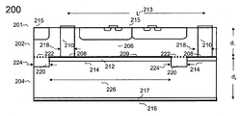
이제 도 2c를 참조하면, X선들을 탐지하도록 된 모놀리식 화소 검출기(201)의 제3 실시예(200)는 얇은 판독 웨이퍼(202)와 흡수체 웨이퍼(204) 사이의 접착 계면을 포함할 수 있다. 판독 웨이퍼는, 예를 들면 모든 처리가 완료된 후 약 10㎛ 내지 30㎛ 또는 바람직하게는 약 5㎛ 내지 10㎛ 또는 심지어 3㎛ 내지 5㎛의 두께까지 얇아지는 바람직하게는 약 1㏀㎝ 내지 2㏀㎝ 또는 심지어 2㏀㎝ 내지 5㏀㎝의 높은 저항률로 약하게 p-도핑된 기판(206)을 CMOS 처리함으로써 제작되었다. 얇게 하는 것은 기판(206)이 얇아질 수 있기 전에 CMOS 스택의 평탄화 및 캐리어 웨이퍼의 본딩을 요구할 수 있다. 흡수체 웨이퍼(204)는 바람직하게는 저항률이 크게 가볍게 p-도핑될 수 있고, 무겁게 도핑된 임플란트 또는 무겁게 도핑된 에피텍셜 층들일 수 있는 고전도성인 n+-도핑된 영역들(212)을 포함할 수 있다. 예를 들어 전도도가 높은 영역들(212)의 도핑 수준은 각각 약 5mΩ㎝ 내지 20mΩ㎝, 0.7mΩ㎝ 내지 5mΩ㎝ 및 0.2mΩ㎝ 내지 0.7mΩ㎝ 사이에 있는 저항률에 대응하는 1×1018cm-3내지 1×1019cm-3 또는 바람직하게는 1×1019cm-3 내지 1×1020cm-3 또는 심지어 1×1020cm-3 내지 5×1020cm-3일 수도 있다. 선택적으로, 흡수체 웨이퍼(204)는 금속 백 컨택(216)과의 옴 접촉 형성을 용이하게 하는 무겁게 p-도핑된 층(217)을 더 포함할 수 있다. 접착 계면은 기판(206)을 통해 확장되는 유사한 도핑 수준들 가진 고전도성인 n+-도핑된 플러그(210)들과, 흡수체 웨이퍼의 전도성인 n+-도핑된 영역들(212) 사이의 공유 반도체 접합(208)으로 이루어질 수 있고, 그로 인해 낮게 도핑된 기판(206)의 흡수체 웨이퍼를 향하는 영역들의 무겁게 도핑된 영역들(212)의 부분 사이에 옴 접촉과 전도성이 빈약한 공유 반도체 본드(209)를 형성한다. 전도성이 빈약한 공유 반도체 본드들(209)은 옴 전도성 본드들(208)보다 적어도 103 내지 104, 또는 바람직하게는 104 내지 106또는 더 바람직하게는 106 내지 108배 더 높은 저항률을 가진다. 무겁게 도핑된 플러그들(210)은 예를 들면 가볍게 p-도핑된 기판(206)에서의 에칭 구멍들에 의해 형성될 수 있고, 그것들을 후속하는 에티펙시 단계에서 n+-재료로 채우는 것은 관련 분야에 알려져 있다. 무겁게 n-도핑된 영역들(21)에 접합된 무겁게 도핑된 플러그들(210)은 전하 컬렉터들의 역할을 하고 흡수체(204)에 입사하는 전자기 방사선에 의해 생성되고 전압을 흡수체 웨이퍼(204) 상의 백 컨택(216)에 인가시 웨이퍼(204)의 가볍게 p-도핑된 벌크와 n-도핑된 영역들(212) 사이의 역 바이어스된 p-n 접합(214)의 전기장에서 분리되는 전자-정공 쌍들로부터 전자들을 수집한다. 그러므로 소수 캐리어들(전자들)은 트래핑과 재결합이 발생할 수 있는 낮게 도핑된 웨이퍼들 사이의 전도성이 빈약한 접착 계면을 절대 가로질러 이동하지 않는다. 전하 컬렉터들(210)는 전자기 방사선에 의해 발생하는 전하 펄스들이 처리되어 판독 전자기기의 오프-화소 부분으로 전달되는 판독 웨이퍼(202)의 화소 판독 전자기기(215)와 통신한다. 검출기 화소들은 그 폭이 예를 들면 약 0.5㎛ 내지 2㎛ 이내 또는 바람직하게는 약 0.5㎛ 내지 1㎛ 이내일 수 있는 무겁게 도핑된 플러그들(210)에 의해 규정된다. 플러그들(210) 사이의 거리(L)은 약 100㎛ 내지 200㎛, 50㎛ 내지 100㎛ 또는 20㎛ 내지 50㎛ 또는 심지어 5㎛ 내지 20 ㎛의 넓은 범위 내에서 변할 수 있는 화소 크기(213)를 규정한다. 흡수체 웨이퍼(204)에서의 무겁게 도핑된 영역들(212)은 적어도 103 내지 104 또는 바람직하게는 104 내지 106, 또는 더 바람직하게는 106 내지 108인 인자만큼 본드(208)의 저항을 초과하는 저항을 갖는 흡수체 웨이퍼와 판독 웨이퍼 사이의 실질적으로 전기 절연성인 반도체-대-산화물 또는 산화물-대-산화물 본드(222)를 형성하는 절연 산화물 영역들(220)에 의해 둘러싸인다. 이들 산화물 영역들의 목적은 인접한 화소들을 서로 전기적으로 절연시키는 것이다. 그것들의 폭(224)은 화소 검출기(200)의 바라는 속력에 의존적인 흡수체 웨이퍼(204)의 무겁게 도핑된 영역들(212)의 폭(226)보다 작거나 같거나 더 클 수 있고, 이러한 바라는 속력은 또한 무겁게 도핑된 영역(212)의 폭(226)에 의해 규정된 커패시터 플레이트의 크기에 의존적이다. 무겁게 도핑된 영역(212)의 폭(226)이 바람직하게는 예를 들면 화소 크기(213)의 2배 또는 3배만큼 더 크거나 심지어 화소 크기(213)의 90%만큼 큰 것처럼 무겁게 도핑된 플러그들(210)의 폭(218)보다 크게 되도록 선택되기 때문에, 본딩 정렬을 위한 요구 사항은 실시예(100)에서보다 더 완화된다.Referring now to FIG. 2C, a
실시예(200)에 따른 화소 검출기는 흡수체 웨이퍼(204)에서 X선들에 의해 생성된 전자-정공 쌍들로부터 전자들을 검출하기 위해 설계된다. 이 실시예의 일 양태에서 검출기는 도핑 부호들을 거꾸로 함으로써 정공 수집을 위해 설계될 수 있다. p-도핑된 영역들의 도핑 수준들은 위에서 논의된 n-도핑된 영역들의 도핑 수준들과 거의 같을 수 있다. n-도핑 경우에 대해서처럼 비슷한 저항률 수준들을 위해서는 약 1.5인 인자만큼 다소 더 높은 도핑이 필요하다.The pixel detector according to the
그것의 설계에 따르면(도 2c 참조), 흡수체 웨이퍼(204)에서의 산화물 영역들(220)이 본질적으로 화소 크기(213)만큼 떨어져 있고 추가적인 화소 격리의 역할을 하기 때문에 실시예(200)는 판독 웨이퍼(202)와 흡수체 웨이퍼(204)의 정밀한 상호 정렬을 필요로 한다. 또한 무겁게 도핑된 플러그(210)들과 무겁게 도핑된 영역(212)들은 본딩 공구에서 정렬될 필요가 있다. 정확한 정렬을 허용하기 위해 얇은 판독 웨이퍼(202)와 흡수체 웨이퍼(204)는 모두 적어도 2개의 특별한 웨이퍼 특징들을 구비하고, 이러한 특징들은 예를 들면 반대 측들에서 웨이퍼 가장자리들에 가깝게 위치한 정렬 마크들의 형태를 가진다. 이러한 정렬 마크들의 중첩의 도움으로 200 mm 웨이퍼들의 회전 오정렬은 약 5×10⁻⁴°미만으로 유지될 수 있고, 그 측면 오정렬은 1㎛ 미만으로 유지될 수 있다. 웨이퍼 본딩이 더 작은 경우에도 유사한 정확도를 얻을 수 있다.According to its design (see Fig.2c),
이제, 도 2d를 참조하면 X선을 검출하게 된 모놀리식 화소 검출기(201')의 제4 실시예(200')는 얇은 판독 웨이퍼(202')와 흡수체 웨이퍼(204') 사이의 접착 계면을 포함할 수 있다. 예를 들면, 이러한 판독 웨이퍼는 모든 처리가 완료된 후, 약 10㎛ 내지 30㎛ 또는 바람직하게는 약 5㎛ 내지 10㎛ 또는 심지어 3㎛ 내지 5㎛까지 얇아지는 바람직하게는 약 1㏀㎝ 내지 2㏀㎝ 또는 심지어 2㏀㎝ 내지 5㏀㎝의 저항률을 갖는 약하게 p-도핑된 기판(206')을 CMOS 처리함으로써 제작될 수 있었다. 얇게 하는 것은 CMOS 스택의 평탄화를 요구할 수 있고, 기판(206') 전의 캐리어 웨이퍼의 본딩은 얇아질 수 있다. 흡수체 웨이퍼(204')는 무겁게 도핑된 인플란트들이거나 무겁게 도핑된 에피텍셜 층들일 수 있는 고전도성의 n+-도핑된 영역들(212')을 포함할 수 있다. 전도성이 높은 영역들(212')의 도핑 수준은 예를 들면 각각 약 5mΩ㎝ 내지 20mΩ㎝, 0.7mΩ㎝ 내지 5mΩ㎝ 및 0.2mΩ㎝ 내지 0.7mΩ㎝ 사이의 저항률에 대응하는 1×1018cm-3 내지 1×1019cm-3 또는 바람직하게는 1×1019cm-3 내지 1×1020cm-3또는 심지어 1×1020cm-3 내지 5×1020cm-3 사이일 수 있다. 선택적으로, 흡수체 웨이퍼(204')는 무겁게 p-도핑된 층(217)을 더 포함하여, 금속 백 컨택(216')과의 옴 접촉 형성을 용이하게 할 수 있다. 접착 계면은 기판(206')을 통하여 확장되는 고전도성인 n+-도핑된 플러그들(210')과 흡수체 웨이퍼(204')의 전도성 n+-도핑된 영역들(212')사이의 전도성인 공유 반도체 본드(208')로 이루어질 수 있다. 플러그들(210')의 도핑 수준은 영역들(212')의 도핑 수준과 유사하며, 두 지점 사이의 온 접촉을 보장한다. 웨이퍼들(202', 204') 사이의 접착 계면은 또한 낮게 도핑된 기판(206')의 흡수체 웨이퍼 향하는 영역들의 무겁게 도핑된 영역들(212')의 부분 사이에 전도성이 빈약한 공유 반도체 본드(209')를 포함한다. 전도성이 빈약한 반도체 본드들(209')은 옴 전도성 본드들(208')보다 적어도 103 내지 104, 또는 바람직하게는 104 내지 106, 또는 더 바람직하게는, 106 내지 108배 더 높은 저항률을 가진다. 예를 들면 도 2d에는 하나만 도시되어 있는 무겁게 도핑된 플러그들(210')이 가볍게 p-도핑된 기판(206')에서 에칭 구멍들에 의해 형성될 수 있고, 이어지는 에피텍시 단계에서 그러한 에칭 구멍들을 n+-재료를 채우는 것은 관련 분야에 알려져 있다. 무겁게 도핑된 영역들(2112')에 접합된 무겁게 도핑된 플러그들(210')은 2개 사이에 옴 접촉을 형성하고 전하 컬렉터들로서의 역할을 하며, 흡수체(204') 상에 입사한 전자기 방사선에 의해 생성되고 흡수체 웨이퍼(204') 상의 백 컨택(216')에 전압을 인가시 많이 n-도핑된 영역들(212')과 가볍게 p-도핑된 기판(206') 사이에 역 바이어스된 p-n 접합(214')의 전기장에서 분리되는 전자-정공 쌍들로부터 전자들을 수집한다. 따라서 소수 캐리어들(전자들)은 트래핑과 재결합이 발생할 수 있는 낮게 도핑된 웨이퍼들 사이의 전도성이 빈약한 접착 게면을 절대 가로질러 움직이지 않는다. 전하 컬렉터들(210')은 전자기 방사선에 의해 발생된 전하 펄스들이 처리되고 판독 전자기기의 오프-화소 부분으로 전달되는 판독 웨이퍼(202')의 화소 판독 전자기기(215')와 통신한다. 검출기 화소들은 무겁게 도핑된 플러그들(210')에 의해 규정되고, 그 폭(218')은 예를 들면 약 0.5㎛ 내지 2㎛ 이내 또는 바람직하게는 약 0.5㎛ 내지 1 ㎛ 이내의 범위에 있을 수 있다. 플러그들(210') 사이의 거리(L)는 약 100㎛ 내지 200㎛, 50㎛ 내지 100 ㎛ 또는 20㎛ 내지 50㎛ 또는 심지어 5㎛ 내지 20 ㎛ 내의 넓은 범위에서 변할 수 있는 화소 크기(213')를 규정한다. 흡수체 웨이퍼(204')에서의 무겁게 도핑된 영역들(212')은 폭(224')이 예를 들면 약 0.5㎛ 내지 2㎛ 이내 또는 바람직하게는 약 0.5㎛ 내지 1 ㎛ 이내일 수 있는 산화물 영역들(220')에 의해 둘러싸인다. 산화물 영역들(220')은 판독 웨이퍼(202')를 통해 확장하는 산화물 채워진 트렌치(trench)들과 흡수체 웨이퍼(204') 사이의 전기적으로 절연하는 산화물-대-산화물 본드들(222')을 형성한다. 폭 트렌치들(226')은 바람직하게는 산화물 영역들(220')의 것과 거의 같다. 산화물 영역들(220', 226')은 인접 화소들을 서로 격리하고, 그것들의 간격은 다시 화소 크기(L)에 대응한다. 무겁게 도핑된 영역들(212')이 화소 크기(213')의 대부분을 차지하기 때문에 실시예(200)와 유사하게 본딩 정렬이 이 경우 촉진된다.Now, referring to FIG. 2D, the
실시예(200')에 따른 화소 검출기는 흡수체 웨이퍼(204')에서 X선이 생성하는 전자-정공 쌍들로부터 전자들을 검출하기 위해 설계된다. 이 실시예의 일 양태에서 검출기를 적절한 도핑 부호들을 거꾸로 함으로써 정공 수집을 위해 설계될 수 있다. p-도핑된 영역들의 도핑 수준은 위에서 논의한 n-도핑된 수준과 거의 같을 수 있다. n-도핑 경우와 유사한 저항률 수준들을 위해서는 약 1.5배 높은 도핑이 필요하다.The pixel detector according to the embodiment 200' is designed to detect electrons from electron-hole pairs generated by X-rays in the absorber wafer 204'. In one aspect of this embodiment, the detector can be designed for hole collection by inverting the appropriate doping codes. The doping level of the p-doped regions may be approximately the same as the n-doped level discussed above. About 1.5 times higher doping is required for resistivity levels similar to the n-doping case.
그것의 설계(도 2d 참조)에 따르면, 실시예(200')는 본딩을 위해 판독 웨이퍼(202')와 흡수체 웨이퍼(204')의 정밀한 상호 정렬이 필요한데, 이는 흡수체 웨이퍼(204')의 산화물 영역들(220')과 판독 웨이퍼(202')의 절연 산화 영역들(226')이 본질적으로 화소 크기(213')로 간격을 두고 접착 계면(222')를 형성하는 동안 일치해야 하기 때문이다. 무겁게 도핑된 플러그(210')들과 무겁게 도핑된 영역(212')들은 접착 계면(208')에서 옴 접점을 형성하기 위해 동등하게 정렬될 필요가 있다. 정확한 정렬을 허용하기 위해 얇은 판독 웨이퍼(202')와 흡수체 웨이퍼(204')는 모두 적어도 2개의 특별한 웨이퍼 정렬 특징들을, 예를 들면 반대 측들 상의 웨이퍼 가장자리들에 가깝게 위치한 정렬 마크들의 형태로 구비한다. 이러한 정렬 마크들의 중첩을 통해 200mm 웨이퍼들의 회전 오정렬은 약 (2-5)×10-4°내에서, 측면 오정렬은 약 0.5㎛ 내지 1㎛ 이내로 유지될 수 있다. 웨이퍼 본딩이 더 작은 경우에도 유사한 정확도를 얻을 수 있다.According to its design (see Fig. 2D), the embodiment 200' requires precise mutual alignment of the read wafer 202' and the absorber wafer 204' for bonding, which is the oxide of the absorber wafer 204'. This is because the
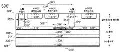
이제, 도 2e를 참조하면, 적외선 방사선을 탐지하도록 된 모놀리식 화소 검출기(301)의 제5 실시예(300)는 얇은 판독 웨이퍼(302)와 흡수체 웨이퍼(304) 사이의 접착 계면을 포함할 수 있다. 판독 웨이퍼는 예를 들어 저항률이 약 0.1㏀㎝ 내지 1㏀㎝인 CMOS 처리 p-도핑된 기판(306)에 의해 제작되었을 수 있다. 판독 웨이퍼(302)는 예를 들면 n-웰들(317)에서의 p-MOS 트랜지스터들과 p-웰들에서의 n-MOS 트랜지스터들을 포함하는 화소 전자 장치(315)의 처리가 완료된 후 약 10㎛ 내지 30㎛ 또는 바람직하게는 약 5㎛ 내지 10㎛ 또는 심지어 더 바람직하게는 약 3㎛ 내지 5㎛ 사이에 있는 두께까지 얇아진다. 얇아지는 것은 CMOS 스택의 평탄화를 요구할 수 있고, 기판(306)이 얇아질 수 있기 전에 캐리어 웨이퍼의 본딩을 요구할 수 있다. 바람직하게, 판독 웨이퍼(302)는 고저항성의 영역들(320)에 의해 둘러싸인 무겁게 n-도핑된 고전도성의 영역들(312)을 포함하고, 후자는 상호 전기적 화소 격리의 역할을 한다. 영역들(312)의 도핑은 예를 들면 각각 약 5mΩ㎝ 내지 20mΩ㎝, 0.7mΩ㎝ 내지 5mΩ㎝ 및 0.2mΩ㎝ 내지 0.7mΩ㎝ 사이의 저항률에 대응하는 1×1018cm-3 내지 1×1019cm-3 또는 바람직하게는 1×1019cm-3 내지 1×1020cm-3또는 심지어 1×1020cm-3 내지 5×1020cm-3 사이일 수 있다. 고저항성 영역들(320)의 저항률은 고전도성 영역들(312)의 것에 대해 적어도 약 103 내지 104, 또는 바람직하게는 104 내지 106, 또는 더 바람직하게는 106 내지 108인 인자만큼 더 높다. 영역들(312, 320)은 예를 들면 낮게 도핑된 기판(306)이 화학 기상 증착에 의해 에피텍셜 성장하기 전에 각각 도펀트들 또는 산소에 의해 얇은 SOI 웨이퍼들을 이온 이식함으로서 형성될 수 있다. 대안적으로, 무겁게 도핑된 영역들(312)과 고저항성 영역들(320)은 또한 판독 웨이퍼(302)를 얇게 만든 후 후면(backside) 처리에 의해 형성될 수 있다. 무겁게 도핑된 영역들(312)은 유사한 도핑 수준들을 가지고 낮게 도핑된 기판(306)을 통해 확장하는 고전도성의 n+-도핑된 플러그(310)들과 옴 접촉들(322)을 형성할 수 있다. 흡수체 웨이퍼(304)는 임의로 무겁게 도핑된 임플란트 또는 무겁게 도핑된 에피텍셜 층일 수 있는, 패턴화되지 않은 고전도성 n+-도핑된 층(326)을 포함할 수 있고, 이는 판독 웨이퍼(302)의 무겁게 도핑된 영역들(312)과의 전도성 공유 반도체 본드를 형성한다. 도핑된 층(326)의 도핑 수준은, 예를 들면 1×1018cm-3 내지 1×1019cm-3또는 바람직하게 1×1019cm-3 내지 1×1020cm-3또는 심지어 1×1020cm-3 내지 5×1020cm-3사이에 있을 수 있다. 고저항성 영역들(320)을 향하는 층(326)의 부분은 예를 들면 산화물 영역들과 같이 영역들(320)이 고저항성 반도체 영역들인지 또는 절연 영역들인지에 따라서 전도성이 빈약한 공유 반도체나 반도체-대-절연체 본드(309)를 형성할 수 있다. 어느 경우든 본드(309)의 저항은 본드(308)의 저항보다 적어도 103 내지 104, 또는 바람직하게는 104 내지 106, 또는 더 바람직하게는 106 내지 108인 인자만큼 초과한다. 흡수체(304)는 층(326) 옆에 낮게 도핑된 적외선 흡수 층(328)을 더 포함할 수 있고, n-도핑된 전하 영역(330), 진성 또는 고저항성의 p--도핑된 전하 증배 층(332) 및 무겁게 p-도핑된 애노드 영역(334)이 있는 애벌랜치 다이오드 또는 p-i-n 다이오드를 포함하는 층들의 스택을 더 포함할 수 있다.Referring now to Fig. 2E, a
실시예(300)의 설계에서, 도핑된 영역들(312)과 접촉하는 도핑된 플러그들(310)은 전하 컬렉터들로서 역할을 하고, 예를 들면 흡수층(328) 상에 입사한 적외선 복사선에 의해 만들어진 구멍들이 검출기가 작동중이고 항복 전압(VB) 위의 역 바이어스가 투명하거나 화소로 된(pixelated) 백 컨택(316)에 인가되는 동안 전하 증배 층(332)에서 애벌랜치 전류를 일으킬 때 애벌랜치 항복(avalanche breakdown)에 의해 생성된 전자들을 수집한다. 층들(328, 330, 332, 334)의 도핑 수준들은 바람직하게는 전하 증배 층(332)에 가장 높은 전기장이 존재하는 것을 보장하기 위해 바람직하게 선택되고 흡수 층(328)에서의 필드는 단지 전하 증배 영역 내로 정공들이 표류하게 하기에 충분히 크다. 따라서 층(328)의 도핑은 예를 들면 1014㎝-3 내지 1015㎝-3일 수 있고, 층(330)의 도핑은 약 5×10¹⁶㎝-3 내지 5×10¹⁷㎝-3일 수 있으며, 층(332)의 도핑은 약 5×10¹⁴㎝-3 내지 5×10¹⁵㎝-3일 수 있고, 마지막으로 층(334)의 도핑은 1019㎝-3 내지 1020㎝-3일 수 있다. X선을 검출하도록 된 실시예들에 유사하게 전하 컬렉터들(310)은 VB 밑으로 바이어스를 낮추기 위해 설계된 담금질(quenching) 회로들을 더 포함하는 판독 웨이퍼(302)의 화소 판독 전자기기(315)와 통신한다(예를 들면, 본 명세서에 전문이 참조로 통합되어 있고 F. Zappa 등에 의한 in Sensors and Actuators A 140, 103(2007)을 참조하라). 검출기 화소들은 무겁게 도핑된 플러그들(310)에 의해 규정되고 그 폭(318)은 예를 들면 약 0.1㎛ 내지 2㎛ 또는 바람직하게는 약 0.5㎛ 내지 1㎛ 내의 범위에 있을 수 있다. 플러그들(310) 사이의 거리(L)는 예를 들면 약 2㎛ 내지 40㎛ 또는 바람직하게는 약 5㎛ 내지 30㎛ 또는 심지어 더 바람직하게는 약 10㎛ 내지 20㎛ 내의 범위에서 변할 수 있는 화소 크기(313)를 규정한다.In the design of
실시예(300)의 설계에서, 흡수 층(328)은 충전 곱셈층 332에 비해 밴드 간격이 낮은 반도체 층이다. 예를 들어 레이어 328은 거의 본질적인 Ge 층이거나 도핑 밀도가 약 10 <15>cm <"3> 미만이고 두께는 약 1 ㎛인 낮은 도핑 층일 수 있다. 충전 영역 330은 약 1 - 5 x 10 < 17>cm <3> 범위의 도핑 밀도와 0.1 ㎛ 정도의 두께를 가진 n 도핑된 GAA 층일 수 있다. 곱셈 계층 332는 약 10 <15>cm <"3>의 도핑 밀도와 0.5㎛ 내지 2㎛ 범위의 두께를 가진 n 도핑된 가아 층일 수 있다. 334계층은 마침내 도핑 수준이 약 5 x 10 < 19>cm <3>이고 두께가 0.5㎛ 내지 1㎛인 중 p 도핑된 가아 층이 될 수 있다. 예를 들어 그러한 레이어 스택으로 구성된 흡수체 웨이퍼는 Ge 기판 웨이퍼에서 GaA 레이어를 전형적으로 성장시켜 매우 밀접하게 격자가 일치하는 방식으로 제작할 수 있다. 308, 309 웨이퍼 본드를 형성하기 전에 Ge 기판 웨이퍼가 얇아져야 하는데, 예를 들어, 먼저 상형 GaA 표면을 캐리어 웨이퍼에 접합한 다음, Ge 기판 웨이퍼를 분쇄 및 화학적 기계적 평면화(CMP) 또는 기술에서 알려진 층 분할(예: LP 참조). J. Appl의 페레인 외 107, 054315 (2010), 본 문서에서 참조에 의해 통합된 전체 공개.In the design of
설계(도 2e 참조)에 따르면, 패턴이 없는 흡수체 웨이퍼 304로 구성된 적외선 검출기 실시예(300)는 X선 검출기에 적용된 화소 검출기에 대해 100'의 구현과 유사한 판독 웨이퍼 302와 흡수체 웨이퍼 304를 본딩 도구에 정확하게 정렬할 필요가 없다. 두 웨이퍼의 회전 오정렬을 약 0.1°내지 0.2°이내로 유지할 수 있는 웨이퍼 제조사가 공급하는 노치 또는 플랫과 같은 웨이퍼 정렬 기능을 겹쳐서 제공되는 대략적인 정렬을 사용할 수 있으며, 예를 들어 얼라인먼트가 제공하는 것처럼 측방향 변위는 약 200㎛ 내지 400㎛ 범위 내에서 사용할 수 있다.EVG580 ComBond 도구의 엔트 및 플리퍼 모듈 따라서 300개의 배기는 판독 및 흡수체 웨이퍼에 추가적인 정렬 표시가 필요하지 않다. 실시예(100 내지 200')의 X선 검출기와 유사하게, 실시예(300)의 적외선 검출기는 가이거 모드에서 작동할 때 단일 광자 검출 능력을 가질 수 있다(예: 센서 및 액추에이터 A 140,103(2007) 참조).According to the design (see Fig. 2e), the
실시예(300)에 따른 화소 검출기는 애벌랜치 층(332)에 있는 전자 정공 쌍에서 전자를 검출하기 위해 설계되었다. 구현 측면에서는 검출기를 적절한 도핑 표시를 반대로 하여 구멍 수집을 위해 설계할 수 있다. p 도핑 지역의 도핑 수준은 위에서 논의한 n 도핑 수준과 거의 같을 수 있다. n 도핑 사례와 유사한 저항성 수준에는 약 1.5배 높은 도핑이 필요하다.The pixel detector according to
이제 도 2f를 참조하면, 적외선을 검출하도록 된 모놀리식 화소 검출기(301')의 제6 실시예(300')는 2개의 접착 계면으을 포함할 수 있다. 첫 번째의 접착 계면(308')은 Si 증배층(332')으로 구성된 얇은 Si 판독 웨이퍼(302)와 두 번째의 얇은 Si 웨이퍼(303) 사이에 위치한다. 두 번째 접착 계면(314')은 두 번째 얇은 Si 웨이퍼(303')와 흡수체 층 스택(305') 사이에 있으며, 이 스택은 함께 흡수체 웨이퍼 304'를 형성한다.Referring now to FIG. 2F, a sixth embodiment 300' of a monolithic pixel detector 301' adapted to detect infrared rays may include two bonding interfaces. The first
예를 들어, 판독 웨이퍼는 약 0.1㏀cm 내지 1㏀cm의 저항성을 가진 CMOS 공정 p 도핑 기판 306에 의해 제작되었을 수 있다. 판독 웨이퍼 302는 약 10㎛ 내지 30㎛ 두께로 얇게 제작되거나, 화소 전자 315를 처리한 후 가급적 약 5㎛ 내지 10㎛로 제작되었다. n-웰들(317')의 p-MOS 트랜지스터와 p-웰들(319)의 n-MOS 트랜지스터가 완료되었다. 박리는 CMOS 스택의 평면화와 캐리어 웨이퍼의 본딩이 필요할 수 있으며, 기판 306'을 박리할 수 있다. 마찬가지로, 첫 번째 접합 계면(308')을 구성한 후 레이어 분할 기법을 사용하지 않는 한, 두 번째 Si 웨이퍼 303'의 박리는 씬닝 전에 캐리어 웨이퍼 본딩이 필요할 수 있다. 가급적 판독 웨이퍼 302에는 고저항 영역 320'으로 둘러싸인 N 도핑, 고 전도성 영역 312가 포함되어 있어 상호 전기 화소 분리를 지원한다. 예를 들어 312 구역의 도핑은 각각 약 5mΩcm 내지 20mΩcm, 0.7mΩcm 내지 5mΩcm, 0.7mΩcm 내지 5mΩcm, 0.2 ιηΩ 0.2 <χ> 사이의 저항성에 해당하는 1 <χ>10 >- 1 x 10 >cm<"3> 사이일 수 있다. 320' 고저항 지역의 저항성은 약 10 <3>- 10 <4>- 10 <6>, 혹은 심지어 10 <6>- 심지어 10 <8>의 고전도 영역과 관련하여 적어도 10 <3>- 10 <4>의 저항성은 더 높으며, 본드 309의 저항성은 최소한 103 내지 104를 초과한다.. 예를 들어, 영역(312와 320')은 도펀트 원자나 산화 원자에 의한 화학 증기에 의해 각각 성장하기 전에 얇은 SOI 웨이퍼에 의해 형성될 수 있다. 도핑 수준이 유사하고 도핑 수준이 낮은 도핑 기판 306'을 통해 확장되는 나체 도핑 플러그의 전도도가 높은 영역과 함께 헤비 도핑 지역 312가 옴 접점 322를 형성할 수 있다. 공유 반도체 본드 314'는 305'의 흡수층 스택의 적외선 흡수층 328'과 두 번째로 얇은 Si 웨이퍼 303의 충전층 334' 사이에 형성된다. 실리콘 p-i-n 또는 애벌랜치 다이오드는 높은 저항성, 내성 또는 매우 낮은 도파형 전하 증배 영역 332초, 공유 반도체 본드 308' 및 p-도파형 전하층 334에 접합된 도파형 웨이퍼 302 사이에 형성된다. 구현 측면에서는 전체 Si 충전 증배 영역이 판독 웨이퍼 302'의 일부일 수 있다. 이 구현의 측면에서는 첫 번째 영역 312', 320', 332', 334'가 Si 웨이퍼를 처리하여 형성될 수 있다. 예를 들어, 에피텍셜 성장 및/또는 이온 이식 등이 그것이다. 이후, 에피텍셜층 306'은 CVD에 의해 증가된 후 CMOS가 처리되어 충전기 318과 함께 화소 판독 전자 장치 315'를 생성할 수 있다. 이 경우 303'의 얇은 Si 웨이퍼 본딩이 필요하지 않다. 이 경우 Si 판독 웨이퍼 302와 흡수체 층 스택 305의 적외선 흡수 계층 328' 사이에 단일 공유 반도체 본드 314'가 존재한다. 구현 300' 설계에서 도핑된 플러그 310' 접촉 도핑된 도핑된 영역 310'은 충전 수집기 역할을 하며, 예를 들어 애벌랜치 항복에 의해 생성된 전자를 수집하는데, 이때 흡수층 328'에서 적외선 방사선에 의해 생성된 전자는 검출기가 오페라에 있는 동안 증배층 332에서 애벌랜치 전류를 발생시킨다.분해 전압 이상의 tion 및 역방향 바이어스 VB는 투명 또는 화소 백 컨택 316'에 적용된다. 328, 332 및 334'의 도핑 수준은 가장 높은 전기장이 곱셈 계층 332에 존재하도록 보장하기 위해 선호되는 반면, 흡수 계층 328'의 장은 전자가 전하 곱셈 영역으로 표류하게 할 만큼 충분히 크다. 따라서 흡수층 328'의 도핑은 예를 들어 10 <14>- 10 <15>cm <3>, 약 5 <χ>lO <16>- 5 x lO <17>cm<3>, 약 5 <χ>10 <14>- 5 x lO <15cm>3>, 마지막으로 약 33-194 <의 도핑이 될 수 있다. X선 감지 충전기 310'에 맞게 개조된 구현물과 유사하게, VB 이하로 바이어스를 낮추기 위해 설계된 quenching 회로로 추가로 구성된 Readout 웨이퍼 302의 화소 판독 전자 장치 315'와 통신한다(예: 센서 및 액추에이터 A 140,103(2007 참조). 참조에 의해 통합된). 검출기 화소은 도핑된 플러그의 폭 310' 310'에 의해 정의되며, 이 중 폭은 예를 들어 약 0.1 - 2 μιη 이내 또는 가급적 약 0.5 - 1 ㎛ 이내일 수 있다. 플러그 사이의 거리 310'은 화소 크기 313'을 정의하며, 예를 들어 약 2 - 40 μπι 범위 내에서 또는 가급적 약 5 - 30 μιη 범위 또는 더 바람직한 약 10 - 20 μπι 범위에서 변할 수 있다. 구현 300'의 설계에서 흡수층 328'은 Si 곱셈층 332'의 하나와 관련하여 밴드갭이 낮은 반도체 층이다. 예를 들어 Layer 328'은 거의 본질적인 Ge 층이거나 도핑 밀도가 약 10 <15>cm <"3> 이하인 낮은 도핑 층일 수 있으며 두께는 도핑 층일 수 있다. 충전층 334'는 약 1 - 5 x 10 <17>cm <"3> 범위에서 도핑 밀도와 0.1 ㎛ 정도의 두께를 가질 수 있다. Si 곱셈층 332는 약 10 <15>cm <"3>의 도핑 밀도와 0.5 - 2 ㎛ 범위의 두께를 가질 수 있다. 흡수체 웨이퍼 304'의 선택적 레이어 326'는 마침내 도핑 수준이 약 1<χ>10 <19>- 1<χ>10 <20>cm <3>3>이고 두께 0.5~1㎛로 백접촉 316'과 오히믹 접촉 형성을 용이하게 한다. 두 번째 얇은 Si 웨이퍼 303'은 SOI 웨이퍼로 제작하여, 얇은 판독 웨이퍼 302'에 접합 후 얇아짐이 용이함. 반면 Ge 흡수 웨이퍼 304'는 분쇄와 CMP 또는 기술에서 알려진 바와 같이 층이 갈라진 후에 얇아질 수 있다(예: LP 참조). J. Appl의 페레인 외 107, 054315 (2010), 본 문서에서 참조에 의해 통합된 전체 공개. 구현의 한 측면의 웨이퍼 본드 308', 309', 314' 또는 단일 웨이퍼 본드 314'를 형성하는 프로세스는 웨이퍼 씬닝이 이 단계를 수행하는 데 캐리어 웨이퍼 본딩이 필요하지 않다는 장점을 갖는다.For example, the read wafer may have been fabricated by a CMOS process p-doped
설계(도 2f 참조)에 따르면, 무늬 없는 Si 웨이퍼 303'와 얇은 판독 웨이퍼 302의 접합으로 구성된 적외선 검출기 구현 300'은 본딩 공구에서 웨이퍼를 정밀하게 정렬할 필요가 없다. 흡수체 층 스택 305'도 본딩을 위해 얇은 Si 웨이퍼 303'와 정확하게 정렬할 필요가 없다. 두 웨이퍼의 회전 오정렬을 약 0.1~0.2도 이내로 유지할 수 있는 웨이퍼 제조사가 공급하는 노치 또는 플랫과 같은 웨이퍼 정렬 기능을 겹쳐서 제공되는 대략적인 정렬을 사용할 수 있으며, 예를 들어 얼라인먼트가 제공하는 것처럼 측방향 변위는 약 200~400 ㎛ 범위 내에서 사용할 수 있다.EVG580 ComBond 도구의 엔트 및 플리퍼 모듈 따라서 300'의 배기는 판독 및 흡수체 웨이퍼에 추가적인 정렬 표시가 필요하지 않다. 구현 300 구현과 유사하게 300'은 가이거 모드에서 작동할 때 단일 광자 검출 능력을 제공할 수 있다(예: 센서 및 액추에이터 A 140,103(2007) 참조).According to the design (see Fig. 2f), an infrared detector implementation 300' consisting of bonding of an unpatterned Si wafer 303' and a
이제 도 2g를 참조하면, 적외선을 검출하도록 된 모놀리식 화소 검출기(301")의 실시예(300")는 얇은 판독 웨이퍼(302")와 흡수체 웨이퍼(304") 사이의 접착 계면을 포함할 수 있다.Referring now to FIG. 2G, an
예를 들면, 판독 웨이퍼는 약 0.1~1kQcm의 저항성을 가진 CMOS 공정 p 도핑 기판 306"에 의해 제작되었을 수 있다. 판독 웨이퍼 302"는 약 10 - 30 μπι의 두께로 얇게 제작되거나, 화소 전자제품 315"를 처리한 후 가급적 약 5 - 10 ㎛ 또는 더 선호된다.n-wells 317"의 ple p-MOS 트랜지스터와 p-wells 319"의 n-MOS 트랜지스터 및 추가 deep n-wells 321"이 완료되었다. 박리는 CMOS 스택의 평면화와 캐리어 웨이퍼의 본딩이 필요할 수 있으며, 기판 306"을 박음질할 수 있다. 판독 웨이퍼 302"는 구멍 수집을 위해 고도로 전도성이 높고 p 도핑된 임플란트 310"을 포함할 수 있다. 전자 수집기 310, 구현물 300, 300'의 310'과 대조적으로, 구멍 수집기 310"은 판독 웨이퍼의 전체 두께를 통해 확장할 필요가 없다. 깊은 n-wells 321" p-wells 319"가 구멍을 모으는 것을 방지한다. 예를 들어 임플란트의 도핑 310"은 1×10¹⁸- 1 10 cm-3 또는 1 <χ>10 <19>- 20>cm <3> 사이일 수 있으며, 5 - 20 mQ cm, 0.7 - 0.7 - 0.2 cm 사이의 저항성에 해당할 수도 있다. 판독 웨이퍼 302"와 흡수체 웨이퍼 304" 사이의 본딩 인터페이스는 낮은 p 도핑 Si 기판 306"과 높은 전도성, 높은 p 도핑 레이어 312" 사이의 공유 반도체 본딩 308"과 결합 309"로 구성될 수 있으며, 이는 지역에 따라 전도성이 낮은 공유 반도체 또는 반도체 대 인슐레이터 본딩 본딩의 결합이 될 수 있다. 인접한 화소을 전기적으로 격리하는 320"은 저항성이 높은 반도체 영역 또는 산화물과 같은 절연체 영역이다. 어쨌든 320"의 저항성은 약 10 <3>- 10 <4>- 10 <6>의 인수로 더 높거나, 또는 고도로 전도된 지역 312"에 관해서도 10 <6>- 10 <8>만큼 높아서, 적어도 10 <3>의 인자로는 308"의 결합 저항이 308"을 초과하게 된다. 또는 10 <6>- 10 <8>을 더 선호한다. 흡수체 웨이퍼 304"는 매우 약한 n 도핑 또는 내충전 증배층 332"와 더 높은 n 도핑 충전층 334"로 구성될 수 있다. 따라서 p-i-n 또는 애벌랜치 다이오드는 p-doyped 영역 312", 내적 또는 매우 낮은 도핑된 전하 곱셈 영역 332" 및 n-도핑된 전하 레이어 334" 사이에 형성된다. 상기 p-i-n 다이오드 흡수체 웨이퍼 304"와 인접하여 내부 또는 가급적 경량 p-도핑 흡수층 328" 및 최종적으로 옵션인 백 컨택 316"로 구성될 수 있다.For example, the read wafer may have been fabricated by a CMOS process p-doped
따라서 실시예(300")의 설계에서 p 도핑된 임플란트 310"은 애벌랜치에 의해 생성되는 구멍 수집기 역할을 할 수 있다. 예를 들어 흡수층 328"에 대한 적외선 사고에 의해 생성되는 구멍은 검출기가 작동 중일 때 곱셈 계층 332"에서 애벌랜치 전류를 발생시키고 분해 위의 역편향을 일으킬 수 있다. 전압 VB는 투명 또는 화소 백 컨택 316"에 적용된다. 328", 332" 및 334"의 도핑 수준은 가장 높은 전기장이 곱셈 계층 332"에 존재하도록 하기 위해 선택되는 것이 좋으며, 흡수 계층 328"의 장은 구멍이 곱셈 영역으로 드리워질 정도로 충분히 크다. 300' 충전 컬렉터 310"은 구현물 300과 유사하게 VB 이하로 바이어스를 낮추기 위해 설계된 quenching 회로(예: 센서 및 액추에이터 A 140,103(2007) 참조)로 추가로 구성된 판독 웨이퍼 302"의 화소 판독 전자 장치 315"와 통신한다. 참고의 검출기 화소은 도핑이 심한 임플란트 310" 너비 318"에 의해 정의되며, 이 중 범위는 예를 들어 약 0.1㎛ 내지 2㎛ 이내 또는 가급적 0.5㎛ 내지 1㎛이내일 수 있다. 임플란트(310") 사이의 거리(L)는 화소 크기(313")를 정의하며, 예를 들어 약 2㎛ 내지 40㎛ 범위 내에서 또는 가급적 약 5㎛ 내지 30㎛ 범위 내에서 또는 더 바람직하게 약 10㎛ 내지 20㎛ 범위 내에서 다를 수 있다.Thus, in the design of the
실시예(300") 설계에서 흡수층 328"은 충전 곱셈층 332"와 312", 334"가 만들어지는 반도체에 대해 밴드갭이 낮은 반도체 층이다. 예를 들어 레이어 328"은 거의 본질적인 Ge 층이거나 도핑 밀도가 약 10 <15>cm <"3> 미만이고 두께는 약 1 μηι인 낮은 도핑 층일 수 있다. 예를 들어 충전 계층 334", 곱셈 계층 332" 및 중 p-도핑 계층 312"는 GaA 계층일 수 있다. 예를 들어 레이어 312"는 1<χ>10 <18>- 1 10<19>cm <" 3> 사이, 또는 1<χ>10 <20>cm <3> 또는 1<χ>10 <20>- 5<χ>10 <20>cm <3> 사이 수준까지 도핑할 수 있다. 충전층 334"는 약 1 - 5 x 10 < 17>cm <"3> 범위에서 n 도핑 밀도와 0.1 μπι 정도의 두께를 가질 수 있다. 배율층 332"는 약 10 <15>cm <"3>의 도핑 밀도와 0.5 - 2 μιη 범위의 두께를 가질 수 있다. 흡수기 웨이퍼 304"의 선택적 레이어 326"은 최종적으로 도핑 수준이 약 5 10 <19>cm <3>이고 두께 0 5 - 1 μηι로 백 컨택 316"으로 옴 접촉 형성을 용이하게 하는 무거운 p 도핑 지층일 수 있다. 예를 들어 그러한 레이어 스택으로 구성된 흡수체 웨이퍼는 Ge 기판 웨이퍼에서 GaA 레이어를 전형적으로 성장시켜 매우 밀접하게 격자가 일치하는 방식으로 제작할 수 있다. Ge 흡수 웨이퍼 304"는 분쇄 및 CMP에 의해 접합된 후 또는 기술에서 알려진 바와 같이 레이어 분할 후 얇게 할 수 있다(예: LP 참조). J. Appl의 페레인 외 107, 054315 (2010), 본 문서에서 참조에 의해 통합된 전체 공개. 웨이퍼 박리 전에 웨이퍼 본드 308', 309'를 형성하는 프로세스는 이 단계를 수행하는 데 캐리어 웨이퍼 본딩이 필요하지 않다는 장점이 있다.In an
그것의 설계(도 2g 참조)에 따르면, 실시예(300")는 본딩을 위해 판독 웨이퍼 302"와 흡수체 웨이퍼 304"의 정확한 상호 정렬을 필요로 하는데, 이는 흡수기 웨이퍼 304"의 절연 영역 320"이 기본적으로 화소 크기 313"로 간격을 두고 웨이퍼 본딩 중에 임플란트 310" 사이에 배치되어야 하기 때문이다. 정확한 정렬을 위해 얇은 판독 웨이퍼 302"와 흡수체 웨이퍼 304"는 모두 적어도 두 개의 특별한 웨이퍼 정렬 특징을 가지고 있다. 이러한 정렬 마크의 중첩을 통해 200mm 웨이퍼의 회전 오정렬은 약 (2 - 5)<χ>10 <"4>도 내에서, 측면 오정렬은 약 0.5 - 1 μηι 이내로 유지될 수 있다. 웨이퍼 본딩이 작은 경우에도 유사한 정확도를 얻을 수 있다.According to its design (see Fig. 2G), the
실시예(300)와 유사하게, 실시예(300")는 가이거 모드에서 작동할 때 단일 광자 검출 능력을 제공할 수 있다(예를 들면, 본 명세서에 전문이 참조로 통합되어 있고 F. Zappa 등에 의한 in Sensors and Actuators A140,103(2007)을 참조하라).Similar to
이제 도 3a를 참조하면, 예를 들어 화소 판독 전자 장치와 통신하는 418 폭의 410을 상단 보기 400에 따라 화소 크기를 정의하는 망사 크기 L의 사각 그리드에 배치할 수 있다. 도 3b의 상단 뷰(400')는 실시예(200, 300, 300", 300")의 고저항성이거나 산화물 영역들(220, 320, 320")의 예를 보여주고 있으며, 이 경우 묻힌 실질적으로 절연성의 정사각형 메시(mesh)(420)가 화소 격리로서 작용한다. 화소 크기(413)에 따라 전하 컬렉터(410)의 폭(418)과 절연 메시의 폭(424)은 도 2a 내지 도 2g에서 상당히 과장될 수 있다.Referring now to FIG. 3A, for example, 410 having a width of 418 communicating with the pixel reading electronic device may be arranged in a rectangular grid having a mesh size L defining a pixel size according to the
이제 도 4를 참조하면, 얇은 판독 웨이퍼의 제1 실시예(500)의 실현은 다음 제작 단계들을 포함할 수 있다:Referring now to Figure 4, the realization of the
1. 바람직하게는 SOI 웨이퍼일 수 있는 웨이퍼(502)에 Si 기판(504), 산화물 박스(506)를 제공하고 Si 층(508)에 표면(520)을 제공하는 단계. Si 층(508)의 두께(d)는 바람직하게는 약 5㎛ 내지 40㎛의 범위 또는 10㎛ 내지 30㎛의 범위 내에 있어야 하며, 더 나아가서는 약 5㎛ 내지 10㎛의 범위 또는 약 3㎛ 내지 5㎛의 범위 내에 있어야 한다. 저항률이 약 500Ω㎝ 이상이고 바람직하게는 적어도 1㏀㎝ 내지 2㏀㎝ 이상이어야 하며, 바람직하게는 적어도 2㏀㎝ 내지 5㏀㎝ 이상이어야 한다. Si 층(508)은 예를 들면 에피텍셜 층일 수 있다.1. Providing a
2. 웨이퍼(502)의 Si 층(508)을 처리하는 단계로서, 전하 컬렉터들의 역할을 ㅎ하 폭(511)의 무겁게 도핑된 플러그들(510)의 고전도성 영역들의 형성을 포함하고, 그것의 스페이싱(513)은 화소 크기(L)에 대응하며, 그것은 CMOS 처리된 화소 판독 전자기기(515)와 통신한다. X선을 검출하도록 될 때, 화소 크기(L)는 100㎛ 내지 200㎛, 50㎛ 내지 100㎛ 또는 20㎛ 내지 50㎛ 또는 심지어 5㎛ 내지 20㎛의 범위 내에 있을 수 있다. 적외선을 탐지하도록 될 때, 화소 크기(L)는 약 2㎛ 내지 40㎛ 범위 내에서 또는 바람직하게는 약 5㎛ 내지 30㎛ 범위 내에서 또는 더 바람직하게는 약 10㎛ 내지 20㎛ 범위 내에 있을 수 있다. 선택적으로 예를 들면, 반대쪽 가장자리에 가까운 간격으로, 웨이퍼(502)에 정렬 마크 형태로 최소 2개의 특별한 웨이퍼 정렬 특징을 형성한다. 높은 저항성을 갖는 Si 층(508)이 약하게 p-도핑될 때, 전자 수집을 위해 적합하게 되게, 약 5mΩcm 내지 20mΩcm 또는 바람직하게는 약 0.7mΩcm 내지 5mΩcm 또는 심지어 0.2mΩcm 내지 0.7mΩcm(각각 약 1×1018cm-3 내지 1×1019cm-3, 1×1019cm-3 내지 1×1020cm-3및 심지어 1×1020cm-3 내지 5×1020cm-3사이의 도핑 수준들)의 저항률을 가지고 n+-도핑된 전하 컬렉터들(510)이 제공된다. 예를 들면 전하 컬렉터 플러그(510)는 Si 층(508)을 통해 에칭된 후 CVD(화학 증기 증착) 단계에서 n-도핑된 물질로 채워짐으로써 형성될 수 있다. 예를 들면 폭(511)은 0.5㎛ 내지 2.5㎛의 범위 또는 바람직하게는 1㎛ 내지 1.5㎛의 범위일 수 있다. 일반적으로 CMOS 처리는 여기에 부분적으로만 도시되고 수치들을 오버로드하지 않기 위해 다음 내용에서 숫자로만 표시되는 웨이퍼(502)의 Si 표면(520) 위에 다수의 사노하물과 금속 층들의 CMOS 스택(517)을 추가적으로 가져온다. 정공 수집을 허용하려면 층(508)과 전하 컬렉터(510)의 전도 유형을 반전시켜야 한다.2. The step of processing the
3. 가공 웨이퍼 502에 CMOS 517 스택의 표면을 평탄하고 매끄럽게 만들기 위해 CMP에 의해 평면화하고, 산화물과 산화물의 본딩에 대해 루트 평균 제곱(RMS) 표면 거칠기를 약 0.5 nm 이하로 유지하고, 플라즈마 활성화 단계에 의해 평면화된 표면을 활성화한다. 취급 웨이퍼 522에 산화층 524를 제공하고 유사한 플라즈마 활성화 단계로 산화층 526의 표면을 활성화한다.3. Planarize the surface of the
4. 저온산화물-산화물 융합 본딩에 의해 계획화된 CMOS 517 스택의 활성 표면을 접합하고 웨이퍼 522를 취급함으로써 산화 접합 인터페이스 528을 제공한다.4. An
5. 예를 들어 기계적 연삭과 반응성 이온 에칭(RIE)의 조합을 통해 CMOS 처리 웨이퍼 502의 Si 기판 504를 제거하여 얇은 판독 웨이퍼 570을 제공한다. 따라서 산화 박스 506은 에치 스톱으로 작용할 수 있으며, 예를 들어 시층 508의 노출된 표면 530이 에치 스톱으로 작용할 수 있는 수정된 반응 이온 에칭(RIE) 단계에서 제거될 수 있다. 표면 530의 얇은 판독 웨이퍼 570은 도핑된 충전기를 전도하는 표면 532와 고저항층 508의 실질적으로 단열 표면 534로 구성된다.5. A
6. 고저항성 Si 레이어 508의 표면과 훨씬 더 높은 저항성의 536 레이어(예: 표면 부위의 변형을 하거나 산소나 탄소를 주입함)를 선택적으로 제공한다. 도핑된 충전기 전도 표면 532와 고저항층 508, 536의 실질적으로 절연 표면 534로 구성된 표면 530은 약 0.5 nm 미만의 RMS 표면 거칠기로 웨이퍼 본딩을 위해 평평하고 부드럽게 하기 위해 CMP를 적용할 수 있다. 예를 들어 습식 화학 세척 및 플라즈마 활성화에 의해 표면 530의 추가 표면 활성화 단계 후, 박리된 판독 웨이퍼 570은 흡수기 웨이퍼에 공유 웨이퍼 본딩이 준비된다.6. Optionally provide a surface of a highly
이제 도 5를 참조하면, 얇은 판독 웨이퍼의 제2 실시예(600)의 구현은 다음 제작 단계들을 포함할 수 있다:Referring now to Figure 5, the implementation of the
1. 하부 표면 606 및 상부 표면 608에 고저항 Si 웨이퍼 602를 제공하고 도핑이 심한 고전도성 영역 604에 하단 표면 606을 삽입한다. 따라서 하부 표면 606은 도핑된(고저항) 웨이퍼 602의 실질적인 단열 표면 607과 도핑된 임플란트 604의 전도 표면 609로 구성된다. 선택적으로 표면 영역 607의 저항성은 더 높아질 수 있다. 예를 들어, 얇은 층 605를 국소적으로 변형하거나 산화시킴으로써 말이다. 높은 저항성 Si 웨이퍼 602가 약한 p 도핑되었을 때, 도핑이 심한 604는 저항률이 약 5mΩ㎝ 내지 20mΩ㎝인 n+-도핑을 선호하거나, 0.7mΩ㎝ 내지 5mΩ㎝ 또는 0.2mΩ㎝ 내지 0.7mΩ㎝(각각 약 1×10¹⁸㎝-3 내지 1×10¹⁹㎝-3, 1×10¹⁹㎝-3 내지 1×10²⁰㎝-3 및 1×10²⁰㎝-3 내지 5×10²⁰㎝-3)1. Provide a high-
2. Si 취급 웨이퍼 620에 산화층 612를 제공하고, 플라즈마 활성화 단계에 의해 산화층 612의 표면 614를 활성화하여 저온 산화물-산화물 융접 본딩에 대비한다. 선택적으로 CMP에 이식한 웨이퍼 602의 표면 606을 산화한 다음, 플라즈마 활성화 단계에서 활성화하여 저온 산화물과 산화물의 융접 본딩에 대비하도록 한다.2. An
3. 저온 산화물-대-산화물 융합 본딩에 의해 웨이퍼들(602, 620)을 함께 본딩하여 산화물 본드(603)를 형성하는 단계.3. Bonding the
4. 두께(619)가 약 5㎛ 내지 40㎛ 또는 바람직하게는 10㎛ 내지 30㎛ 또는 더 바라직하게는 약 5㎛ 내지 10㎛ 또는 심지어 약 3㎛ 내지 5㎛인 웨이퍼(618)에 본드된 웨이퍼(602)를 얇게 하는 단계로서, 기판(622), 산화물 박스(612) 및 표면(624)을 구비한 Si 층(618)으로 이루어지는 Si 웨이퍼(616)가 생기게 한다. Si 층(618)은 박스(612)에 인접한 무겁게 도핑된 영역들(604)을 포함한다.4. Bonded to a
5. CMOS 프로세싱 SOI 웨이퍼 616의 Si 레이어 618. 화소 크기 L을 정의하고 CMOS 처리 화소 판독 전자 장치 615와 통신하는 613의 폭 610의 고전도성 플러그 영역을 형성하는 것을 포함한다. X선 검출에 적응할 때, 화소 크기 L은 100 - 200 μη, 50 - 100 μπι, 20 - 50 μηι 또는 5 - 20 μπι의 범위 내에 있을 수 있다. 적외선 탐지에 적응할 때, 화소 크기 L은 약 2 - 40 μηι 범위 내에서 또는 가급적 약 5 - 30 μιτι 범위 내에서 또는 더 바람직하게 약 10 - 20 μπι 범위 내에 있을 수 있다. 예를 들어, 반대쪽 가장자리에 가까운 웨이퍼 616 간격의 정렬 표시 형태로 최소 두 개의 특수 웨이퍼 정렬 특징의 형성을 포함한다. 플러그 610은 604번 삽입물과 함께 충전 수집기 역할을 하며, 여기에 오밀 접점으로 전기적으로 연결되어 있다. 높은 저항성 Si 웨이퍼 602가 약한 p 도핑인 경우, 충전기 610은 저항성 약 0.2~10 πιΩ cm의 n<+> 도핑 또는 약 0.2~1 mQ cm(약 5<χ>10 <18>- 5<χ>10 <20>cm의 도핑 수준) 또는 가급적 5 * 1019>- 51020> ~ 3cm의 값이 좋다. 충전 수집기 플러그 610은 예를 들어 Si 레이어 618을 통해 604까지 에칭하여 형성될 수 있으며, 이는 예를 들어 고 도핑 영역 604에 접촉하기 위한 CVD 단계에서 고도로 도핑된 물질로 채워져 있어 충전 수집의 유효 영역을 임플란트 크기로 증가시킬 수 있다. 예를 들어 플러그 610의 폭 611은 0.5 - 2.5 μηι의 범위 또는 가급적 1 - 1.5 μηι의 범위에 있을 수 있다. 일반적으로 CMOS 프로세싱은 여기에 부분적으로만 표시되고 수치 과부하를 일으키지 않기 위해 다음 숫자로만 표시되는 웨이퍼 616의 Si 표면 위에 617의 산화물과 금속 층을 추가로 쌓는다. 구멍 수집을 허용하려면 웨이퍼 602 및 도핑이 심한 지역 604 및 충전 수집기 610의 전도 유형을 반전시켜야 한다.5.
6. 가공 웨이퍼 616의 Si 표면 624 위에 CMOS 스택의 표면 617을 평활화하여 약 0.5 nm 이하의 RMS 표면 거칠기로 산화-산화물 접합에 대해 평탄하고 부드럽게 만들고, 혈장 활성화 단계에 의해 CMOS 스택의 평면화된 표면을 활성화한다. 취급 웨이퍼 630에 산화층 632를 제공하고 유사한 플라즈마 활성 단계로 산화층 634의 표면을 활성화하여 산화물과 산화물의 결합을 준비한다.6. Smoothing the
7. 처리된 웨이퍼(616)의 Si 표면(624) 위에 평면화된 CMOS 스택(617)의 활성 표면과, 저온 산화물-대-산화물 퓨전 본딩에 의해 핸들링 웨이퍼(630)의 활성 표면(634)을 접합하여 접합된 웨이퍼 스택(636)을 형성하는 단계.7. Bond the active surface of the
8. 예를 들면 기계적 연삭과 반응성 이온 에칭(RIE)의 조합을 통해 CMOS 처리 웨이퍼 616에서 취급 웨이퍼 620을 제거하여 얇은 판독 웨이퍼 670을 제공한다. 따라서 산화 박스 612는 에치 스톱으로 작용할 수 있으며, 예를 들어 노출된 표면 606이 저 도핑 웨이퍼 602의 실질적으로 절연 표면 607과 중 도핑된 삽입물 604의 전도 표면 609가 차례로 에치 스톱으로 작용할 수 있는 수정된 RIE 단계에서 제거될 수 있다. 표면 606은 선택적으로 흡수기 웨이퍼와의 공유 결합을 위해 RMS 표면 거칠기가 약 0.5 nm 미만인 얇은 판독 웨이퍼 670을 평평하고 매끄럽게 만들기 위해 CMP를 적용할 수 있다.8. Remove the
이제 도 6을 참조하여 얇은 판독 웨이퍼의 제3 실시예(700)의 실현은 다음 제작 단계들을 포함할 수 있다:With reference now to FIG. 6, the realization of the
1. Si 기판 704, 옥사이드 박스 706 및 Si 레이어 708이 표면 720인 SOI 웨이퍼 제공. Si 레이어 708의 두께 d는 가급적 약 5 - 40 μπι의 범위 또는 10 - 30 μηι의 범위 또는 더 나은 경우 약 5 - 10 μηι 또는 3 - 5 μηι의 범위에 있어야 한다. 저항성이 약 500 Ocm 이상인 저 도핑이어야 하며, 가급적 1 - 2 kQ cm 또는 적어도 2 - 5 kQ cm 이상이어야 한다. Si 레이어 708은 예를 들어 상형 층일 수 있다.1.Provide SOI wafer with
2. CMOS 처리 화소 판독 전자제품 715와 통신하는 충전기 711 및 화소 크기 L에 해당하는 간격 713의 고도로 도핑된 플러그 710의 전도성 영역 형성을 포함하여 웨이퍼 702의 Si 레이어 708 처리. X선 검출에 적응할 때, 화소 크기 L은 100 - 200 μηι, 50 - 100 μηι 또는 20 - 50 μηι 또는 5 - 20 μηι의 범위 내에 있을 수 있다. 적외선 탐지를 위해 개조된 경우, 화소 크기 L은 약 2 - 40 μη 범위 또는 가급적 약 5 - 30 μηι 범위 또는 더 나은 약 10 - 20 μη 범위일 수 있다. 선택적으로 멀리 떨어져 있는 웨이퍼 702에 정렬 마크 형태로 최소 두 개의 특수 웨이퍼 정렬 기능의 형성을 포함한다(예: 반대쪽 가장자리에 가까운 위치). 측면. 예를 들어, 높은 저항성 Si 레이어 708이 약한 p 도핑일 경우, 약 5 - 20 cm cm의 저항성을 가진 n<+> 도핑된 710이 제공되거나, 가급적 약 0.7 - 5 mQ cm 또는 0.2 - 0.7 ιηΩ cm(약 1<χ>10 <18>- 1 10 19 cm>, 1^ 전자 탐지에 적합한 충전 수집기 710은 예를 들어 Si 레이어 708을 통해 구멍을 식각하여 형성될 수 있으며, 이 구멍은 CVD 단계와 같이 N 도핑되지 않은 물질로 채워진다. 예를 들어 폭 711은 0.5 - 2 μιη의 범위 또는 가급적 1 - 1.5 μπι의 범위일 수 있다. 일반적으로 CMOS 프로세싱은 여기에 부분적으로만 표시되며 수치가 과부하되지 않도록 다음 숫자로만 표시되는 웨이퍼 702의 Si 표면 720 위에 717의 산화물과 금속 층을 추가로 쌓는다. 구멍 수집을 허용하려면 웨이퍼(702) 및 전하 컬렉터(710)의 전도 유형을 반전시켜야 한다.2. Processing the
3. CMOS 스택을 가공 웨이퍼 702에 평활하고 부드럽게 하여 산화-산화물 본딩에 적합하도록 CMP에 의한 CMOS 스택을 평면화하고, RMS 표면의 거칠기를 약 0.5 nm 이하로 유지하고, 플라즈마 활성화 단계에 의해 평면화된 표면을 활성화한다. 취급 웨이퍼 722에 산화층 724를 제공하고 유사한 플라즈마 활성화 단계로 산화층 724의 표면 726을 활성화한다.3. Flatten the CMOS stack by CMP to be suitable for oxide-oxide bonding by smoothing and smoothing the CMOS stack on the processed
4. 저온산화물-산화물 융합 본딩에 의해 웨이퍼 702에 평면화된 CMOS 717 스택의 활성 표면을 접합하고 웨이퍼 722를 취급하여 본딩 웨이퍼 스택을 형성한다.4. Bond the active surface of the
5. 예를 들어 기계적 연삭과 반응성 이온 식각(RIE)의 조합을 통해 CMOS 처리 웨이퍼 702 중 기판 704 제거. 따라서 산화상자 706은 에치 스톱으로 작용할 수 있으며, 예를 들어 시층 708의 노출된 표면 730이 에치 스톱으로 작용할 수 있는 수정된 RIE 단계에서 후속적으로 제거될 수 있다.5. Removal of
6. 웨이퍼 취급에 접합된 얇은 판독 웨이퍼 730의 표면 730의 금속 층 740이 낮은 도핑 Si 레이어 708의 쇼트키 장벽을 형성하고 도핑된 충전기 710과 옴 접촉하는 것이 바람직하다. 선택적으로 금속층 740은 표면 730의 일부가 코팅되지 않은 상태로 남아 화소 분리를 위해 742의 개구부를 남기는 리프트오프 프로세스에 축적될 수 있다. 따라서 무늬가 있는 금속층 740은 도핑된 플러그 710과 오밀 접점을 형성하여 전하 수집을 위한 유효 면적을 증가시킨다.6. It is preferred that the
7. 단계 6에서 연속 층으로 퇴적된 경우 금속 레이어 740을 패치가 전도성이 높은 영역을 분리하는 화소 분리를 위한 개구부 742를 형성한다. 따라서 선택적으로 무늬가 있는 금속층 740은 도핑된 플러그 710과 오밀 접점을 형성하여 전하 수집을 위한 유효 면적을 증가시킨다.7. When the
8. 예를 들어 저온 플라즈마 강화된 화학 기상 증착(PECVD) 공정에서 개구부(742)를 채우기 위해 산화물 층(750)을 증착하는 단계로서, 그것에 의해 금속 ㅍ패치들(744) 또한 산화물(752)로 덮여질 수 있다.8. Depositing an
9. 예를 들어 CMP 단계에서 산화물 층(750)을 평탄화함으로써 얇아진 판독 웨이퍼(770)를 제공하고, 그로 인해 개구(742)들에서만 표면(762)에 산화물을 남기고 전도성 금속 표면(764)에는 산화물을 남기지 않는다. 이 단계에서 RMS 거칠기가 약 0.5 nm 미만인 평평하고 매끄러운 표면 766의 얇은 판독 웨이퍼 770의 세 번째 구현이 이제 산화 표면 762와 전도성 금속 표면 764로 구성되며, 이제 흡수체 웨이퍼에 저온 결합을 위한 준비가 완료되었다.9. For example, by planarizing the
이제 도 7a를 참조하면, 흡수체 웨이퍼(850)의 제1 실시예(800)의 실현은 다음 제작 단계들을 포함할 수 있고, 그것의 일부의 순서는 서로 교환될 수 있다:Referring now to Fig. 7A, the realization of the
1. 상부 표면 804 및 하부 표면 806에 흡수체 웨이퍼 802 제공 필요한 경우, 반대쪽 가장자리에 가까운 웨이퍼 802의 상단 표면 804에 정렬 마크 형태로 최소 2개의 특수 웨이퍼 정렬 특징을 형성한다. 웨이퍼 802는 고순도의 단일 결정 Si, Ge, 다이아몬드, SiC, GaA, CdTe 또는 CdZnTe 합금 웨이퍼일 수 있으며, X선 검출에 적합할 경우 가능한 최고의 저항성을 보장하는 데 필요한 범위 내에서만 도핑되는 것이 바람직하다. 예를 들어 Si 웨이퍼의 저항률은 10㏀㎝ 내지 20㏀㎝이고, Ge 웨이퍼는 약 50Ωcm의 저항률을 가지며, SiC는 약 107Ωcm 내지 109Ωcm, GaAs는 약 109Ωcm, CdTe는 약 약 109Ωcm 및 CdZnTe는 약 1010Ωcm의 저항률을 갖는다. 고저항 웨이퍼(802)는 n-전도성이 약하거나 p-전도성이 약할 수 있다. 웨이퍼(802)는 반드시 단일의 균일한 소재로 구성될 필요는 없다. 단결정 기판 웨이퍼에 에피텍셜층을 가진 에피텍셜 웨이퍼가 될 수 있다. X선 검출에 적응할 때, 예를 들어, 에피텍셜층은 CdTe 또는 Cd1-xZnxTe이며, x는 예를 들어 5% 내지 15% 범위 또는 바람직하게는 약 10%의 범위에 있을 수 있고 두께는 예를 들면 200㎛ 내지 500㎛의 범위를 가질 수 있다. 예를 들어, 기판은 에피텍셜 성장 동안 형성되는 유해성 영역을 피하기 위해 Si 또는 Ge 웨이퍼 또는 가급적 GaA, InSb와 같은 III-V 반도체에서 웨이퍼를 사용할 수 있다. 격자 불일치 기판에서의 상형성장의 경우, 탈구 밀도를 낮추기 위해 구성 등급제를 사용하는 것이 유리할 수 있다. 예를 들어, ZnSe는 GaA와 Ge(각각 0.567nm, 0.565nm의 래티스 파라미터)에 근접하게 일치하므로, 예를 들어, 0.648nm의 CdTe의 격자 파라미터까지 등급 매기는 것은 x = 0 ~ x = 1(순수 ZnTe), 0.6nm),o 순수 CdTe 또는 바람직한 Zn 내용. 반면에 InSb 기판을 사용하는 경우 CdTe는 열적으로 일치하는 격자뿐만 아니라 매우 잘 일치하는 격자(등열 팽창 계수)이기 때문에 등급이 매길 필요가 없다. 적외선 탐지에 적응할 때, 흡수체 웨이퍼 802는 예를 들어 Si, Ge, SiGe 합금 또는 SiGeSn 합금으로 구성된 단일 크리스탈 그룹 IV 반도체 웨이퍼 또는 예를 들어 InAs, InGaAs 합금 또는 InSb로 구성된 단일 크리스탈 II/VI 반도체 웨이퍼일 수 있다. HgCdTe 합금. 흡수기 웨이퍼 802는 선택적으로 Si, Ge, GaA, CdTe 또는 CdZnTe 합금과 같은 단일 결정 기판에 얇은 에피텍셜층 형태로 이러한 물질을 구성하는 에피텍셜 웨이퍼일 수 있다. 흡수기 웨이퍼(802)는 실시예(300, 300 및 300")에 따라 도핑된 층을 포함하여 보다 복잡한 구조에서 이러한 재료의 조합을 추가로 구성할 수 있다.1. Provide
2. 웨이퍼 802에 패턴이 있는 전기 절연 유전 마스크 808과 상부 표면 804에 마스크 개구부(창) 812 제공 전자 마스크 808은 가급적 이산화규소(Si02) 마스크로, 808 지역은 산화 지역이다. 마스크 개구부 812의 최소 너비 810은 570, 670, 670, 770의 충전식 수집기 511, 611, 711의 폭과 거의 일치할 수 있다. 마스크 개구부 및 패치 크기 814의 총 폭 813은 판독 전자 장치의 화소 크기(113, 213, 313, 413, 513, 613, 713)와 같다.2. Provide an electrically insulating
3. 예를 들어, 1×1018cm-3내지 1×1019cm-3 또는 바람직하게 1×1019cm-3내지 1×1020cm-3 또는 심지어 1×1020cm-3내지 5×1020cm-3 사이의 레벨로, 에피텍셜 성장 동안에 무겁게 도핑되는 호모-에피텍셜 흡수체 재료(818)로 마스크 개구(812)들을 채워서 고전도성이 되게 하는 단계. 따라서 재료(818)는 측면 에피텍셜 과성장 때문에 주름이 있는 표면(822)을 초래하여 유전체 마스크(808)의 일부를 덮을 수 있다. 채움은 예를 들어 마스크 개구부(812)로 선택적 에피텍셜 성장을 통해 이루어질 수 있다. 예를 들어 채움 재료(818)는 고저항성 웨이퍼(802)에 대한 반대 전도(도핑) 유형의 것일 수 있다.3. For example, 1×1018 cm-3 to 1×1019 cm-3 or preferably 1×1019 cm-3 to 1×1020 cm-3 or even 1×1020 cm-3 to 5 Filling the
4. 선택적으로 도핑된 레이어 820을 제공하며, 예를 들어 검출기의 후방 접점으로 작동하도록 개조된 흡수기 웨이퍼 802의 하부 표면 806에 도핑된 경우 5× 1018cm-3 내지 5×1019cm-3또는 심지어 5× 1019cm-3 내지 5×1020cm-3사이까지 도핑된다. 따라서 층(820)은 예를 들어 에피텍셜 재료(818)와 반대되는 도핑 타입이다. 도핑된 층(820)은 예를 들어 균일하게 성장하는 흡수제 재료와 성장 중 도핑으로 제공될 수 있다. 대안적으로, 무겁게 도핑된 층(820)은 하부 흡수체 표면(806)의 이온 주입에 의해 제공될 수 있다.4. 5×1018 cm-3 to 5×1019 cm-3 if doped on the
5. 예를 들어 에피텍셜 재료(818)와 유전체(808)의 주름진 표면(822)를 평탄화함으로써 약 0.5㎚ 이하의 RMS 거칠기를 가지고 반도체 표면들(826)과 절연 산화물 표면들(827)로 이루어지는 평탄하고 매끄러운 표면(824)을 제공함으로써 흡수체 웨이퍼(850)를 제공한다. 표면(824)의 추가적인 표면 활성화 단계 후, X선 흡수 층(852)을 포함하는 흡수체 웨이퍼(850)는 얇아진 판독 웨이퍼(570, 670 및 770)에 접합할 준비가 된다.5. For example, by flattening the
고전도성 재료 818의 간격이 화소 크기 813을 정의하는 충전기 플러그 510, 610 및 710과 상당히 같기 때문에 시공 흡수기 웨이퍼 850을 본딩 도구의 판독 웨이퍼 570, 670 및 770과 정확하게 정렬할 필요가 있는 것으로 이해된다.It is understood that the
실시예(800)의 일 양태에서, 흡수체 웨이퍼(850)는 이식 단계들에 의해 실현될 수 있는데, 이 경우 전도성이 빈약하거나 절연성인 영역들(808)이 예를 들면 비정질화 또는 산소 또는 탄소 이식에 의해, 그리고 도펀트 이식에 의한 고전도성 재료(818)가 있는 영역들에 의해 형성된다.In one aspect of the
이제 도 7b를 참조하여, 흡수체 웨이퍼(850')의 제2 실시예(800')의 실현이 다음의 대안적인 제작 단계들을 포함할 수 있고, 그 중 일부의 순서는 서로 교환될 수 있다:Referring now to FIG. 7B, the realization of the second embodiment 800' of the absorber wafer 850' may include the following alternative fabrication steps, some of which may be ordered interchangeably:
1. 상부 표면 804' 및 하부 표면 806'의 흡수체 웨이퍼 802 제공 선택적으로, 반대편의 가장자리에 가까운 웨이퍼 802'의 상단 표면 804'에 정렬 마크 형태로 적어도 두 개의 특수 웨이퍼 정렬 특징을 형성한다. 예를 들어 X선 검출에 적응할 때 그룹 IV 반도체 웨이퍼(예: 단일 결정 Si, Ge, SiC 또는 다이아몬드 웨이퍼) 또는 GaAs 웨이퍼와 같은 II I/V 반도체 웨이퍼 또는 CdTe 또는 CdZnTe 합금 웨이퍼)가 모두 순도가 높고 원형이 없거나 원형이 없는 것이 좋다. 각 구성 재료의 최대 가능한 저항성을 보장하는 데 필요한 범위까지만 도핑된다. 예를 들어 Si 웨이퍼의 저항률은 10㏀cm 내지 20㏀cm, Ge 웨이퍼는 약 50Ωcm, SiC는 약 107 내지 109Ωcm, GaA는 약 109Ωcm, CdTe는 약 109Ωcm, CdZnTe 합금 웨이퍼는 약 1010Ωcm이다. 고저항성 웨이퍼(802)는 n-전도성이 약하거나 p-전도성이 약할 수 있다. 웨이퍼(802')는 반드시 단일의 균일한 소재로 구성될 필요는 없다. 단결정 기판 웨이퍼에 에피텍셜층을 가진 에피텍셜 웨이퍼가 될 수 있다. X선 검출에 적응할 때, 예를 들어, 에피텍셜층은 CdTe 또는 Cd1-xZnxTe이며, x는 예를 들어 5% 내지 15% 범위 또는 바람직하게 약 10%이며, 200㎛ 내지 500㎛의 범위를 가지는 두께가 될 수 있다. 예를 들어 기판들은 에피텍셜 성장 중에 형성되는 안티페이스(antiphase) 영역들을 피하기 위해 단결정 Si 또는 Ge 웨이퍼 또는 가급적 GaA, InSb와 같은 III-V 반도체에서 단일 결정 웨이퍼가 될 수 있다. 격자 불일치 기판에서의 상형성장의 경우, 탈구 밀도를 낮추기 위해 구성 등급제를 사용하는 것이 유리할 수 있다. 예를 들어, ZnSe는 GaA와 Ge(각각 0.567nm, 0.565nm의 래티스 파라미터)에 근접하게 일치하므로, 예를 들어, 0.648nm의 CdTe의 격자 파라미터까지 등급 매김으로써, ZnSei-xTex를 x = 0 ~ x = 1(순수 ZnTe), 0.6nTe의 격자를 매김으로써 실현할 수 있다.o 순수 CdTe 또는 바람직한 Zn 내용. 반면에 InSb 기판을 사용하는 경우 CdTe는 열적으로 일치하는 격자뿐만 아니라 매우 잘 일치하는 격자(등열 팽창 계수)이기 때문에 등급이 매길 필요가 없다. 적외선 탐지에 적응할 때, 흡수체 웨이퍼 802는 예를 들어 Si, Ge, SiGe 합금 또는 SiGeSn 합금으로 구성된 단일 크리스탈 그룹 IV 반도체 웨이퍼 또는 예를 들어 InAs, InGaAs 합금 또는 InSb로 구성된 단일 크리스탈 II/VI 반도체 웨이퍼일 수 있다. HgCdTe 합금. 흡수기 웨이퍼 802는 선택적으로 Si, Ge, GaA, CdTe 또는 CdZnTe 합금과 같은 단일 결정 기판에 얇은 에피텍셜층 형태로 이러한 물질을 구성하는 에피텍셜 웨이퍼일 수 있다. 흡수기 웨이퍼 802는 구현물 300, 300 및 300"에 따라 도핑된 층을 포함하여 보다 복잡한 구조에서 이러한 재료의 조합으로 구성될 수 있다.1. Providing
2. 예를 들어 웨이퍼(802) 중 도핑, 고전도성 층(817')의 상부 표면(804') 제공, 예를 들어 1<χ>10<18>- 1<χ>10<19>- 1×10<20>cm<3> 또는 1<χ>10>- 5<χ>10<20>cm<3> 사이 수준으로 도핑된 경우, 이온이나 홈에 의한 예. 레이어 817'은 표면 821'의 연속 필름 형태로 제공될 수 있다. 층(817')은 예를 들어 고저항 웨이퍼(802')와 정반대의 전도(도핑)형일 수 있다.2. For example, doping in the
3. 전기 절연 산화물 영역 808' 폭 814'에 의해 분리된 폭 810'의 중 도핑 지역 818'에 대한 패터닝 층 817' 도핑된 지역 818'의 최소 폭 810'은 약 511, 611, 711의 충전 수집기 510, 610, 710의 얇은 판독 웨이퍼에 해당할 수 있다. 도핑 지역 818'과 산화 지역 808'의 총 폭은 판독 전자 장치의 화소 크기 113, 213, 313, 413, 513, 613, 713, 813'과 같다. 예를 들어 레이어 817'의 패터닝은 그 영역 808'의 너비 814'를 통해 완전히 산화되어 전기적으로 절연되어 웨이퍼 202' 의 골판 표면 822'를 생성함으로써 이루어질 수 있다.3. The patterning layer 817' for the heavy doped region 818' of width 810' separated by the electrically insulating oxide region 808' width 814', the minimum width 810' of the doped region 818' is a charge collector of about 511, 611, 711 It may correspond to a thin read wafer of 510, 610, 710. The total width of the doped region 818' and the oxidized region 808' is equal to the
4. 옵션으로 도핑된 레이어 820'을 제공함. 예를 들어 검출기의 백접점 역할을 하도록 개조된 흡수체 웨이퍼 802의 하부 표면 806'에 도핑하여 5 x 10 < 19>cm<"3> 또는 5 x 10 <19>- 5<χ>10 <20>cm<3> 사이의 레벨로 도핑된다. 따라서 '층 820'은 에피텍셜 물질 818'과 반대되는 도핑 유형의 것이다. 도핑된 층 820'은 예를 들어 하부 흡수기 표면 806의 이온 주입에 의해 제공될 수 있다. 또는 도핑이 심한 820'은 균일하게 성장하는 흡수제 재료와 성장 중 도핑에 의해 제공될 수 있다.4. Optionally doped layer 820' is provided. For example, by doping the lower surface 806' of the
5. 도핑 부위 818' 및 산화 부위 808'을 코팅한 흡수체 웨이퍼 802의 골판 무늬 표면 822'를 계획하여 약 0.5nm 미만의 RMS 거칠기로 평탄하고 매끄러운 표면 824'를 제공함으로써 850'을 공급하고, 반도체 표면 826'과 산화 표면 827'로 구성되어 얇은 면과 결합할 수 있도록 한다. 판독 웨이퍼 570, 670, 770. X선 흡수 레이어 852로 구성된 824' 흡수기 웨이퍼 850'의 추가 표면 활성 단계가 끝나면 얇은 판독 웨이퍼 570, 670 및 770에 접합할 준비가 된다.5. By planning the corrugated patterned surface 822' of the
도핑된 부위 818'의 간격이 화소 크기 813'을 정의하는 충전기 플러그 510, 610, 710과 실질적으로 같기 때문에 구현된 800'의 건설 흡수기 웨이퍼 850'을 판독 웨이퍼 570, 670, 770과 정확하게 정렬할 필요가 있다.Since the spacing of the doped regions 818' is substantially the same as the charger plugs 510, 610, and 710 that define the pixel size 813', the implemented 800' construction absorber wafer 850' needs to be accurately aligned with the read
이제 도 7c를 참조하면 흡수체 웨이퍼(850")의 제3 실시예(800")의 실현은 다음 대안적인 제작 단계들을 포함할 수 있고, 그 중 일부의 순서는 서로 교환될 수 있다:Referring now to Fig. 7C, the realization of the
1. 상부 표면 804" 및 하부 표면 806"과 함께 흡수체 웨이퍼 802" 제공 예를 들어, 반대쪽 가장자리에 가까운 웨이퍼 802"의 상단 표면 804"에 정렬 마크 형태로 적어도 두 개의 특수 웨이퍼 정렬 특징을 형성한다. 예를 들어, X선 검출에 적응할 때 그룹 IV 반도체 웨이퍼(예: 단일 결정 Si, Ge, SiC 또는 다이아몬드 웨이퍼) 또는 GaA 웨이퍼와 같은 II/V 반도체 웨이퍼 또는 CdTe 또는 CdZnTe 합금 웨이퍼)가 될 수 있으며, 이 모든 웨이퍼는 고순도 및 비정형 웨이퍼여야 한다. 각 구성 재료의 최대 가능한 저항성을 보장하는 데 필요한 범위까지만 도핑된다. 예를 들어 Si 웨이퍼의 저항률은 10㏀cm 내지 20㏀cm이고, Ge 웨이퍼는 약 50Ω㎝의 저항률, SiC는 약 107Ω㎝ 내지 109Ω㎝, GaAs는 약 109Ω㎝, CdZnTe는 약 1010Ω㎝이다. 높은 저항성 웨이퍼(802")는 n-전도성이 약하거나 p-전도성이 약할 수 있다. 웨이퍼 802"가 반드시 단일의 균일한 소재로 구성될 필요는 없다. 단일 결정 기판 웨이퍼에 에피텍셜층을 가진 에피텍셜 웨이퍼가 될 수 있다. X선 검출에 적응할 때, 예를 들어, 에피텍셜층은 CdTe 또는 Cd1-xZnxTe이며, 예를 들어 5 - 15% 범위 또는 가급적 약 10%와 200 - 500 μηι의 두께가 될 수 있다. 예를 들어 기판은 에피텍셜 성장 중에 형성되는 항위험 영역을 피하기 위해 단일 결정 Si 또는 Ge 웨이퍼 또는 가급적 GaA, InSb와 같은 III-V 반도체에서 단일 결정 웨이퍼가 될 수 있다. 격자 불일치 기판에서의 상형성장의 경우, 탈구 밀도를 낮추기 위해 구성 등급제를 사용하는 것이 유리할 수 있다. 예를 들어, ZnSe는 GaA와 Ge(각각 0.567nm, 0.565nm의 래티스 파라미터)에 근접하게 일치하므로, 예를 들어, 0.648nm의 CdTe의 격자 파라미터까지 등급 매기는 것은 x = 0 ~ x = 1(순수 ZnTe), 0.6nm), 순수한 CdTe 또는 모든 바람직한 Zn 내용. 반면에 InSb 기판을 사용하는 경우 CdTe는 열적으로 일치하는 격자뿐만 아니라 매우 잘 일치하는 격자(등열 팽창 계수)이기 때문에 등급이 매길 필요가 없다. 적외선 탐지에 적응할 때, 흡수기 웨이퍼 802"는 예를 들어 Si, Ge, SiGe 합금 또는 SiGeSn 합금으로 구성되는 단일 결정 그룹 IV 반도체 웨이퍼 또는 예를 들어 InAs, InGaAs 합금 또는 InSb로 구성되는 단일 결정 II/V 반도체 웨이퍼일 수 있다. HgCdTe 합금. 흡수기 웨이퍼 802"는 선택적으로 Si, Ge, GaAs, CdTe 또는 CdZnTe 합금과 같은 단일 결정 기판에 얇은 에피텍셜층 형태로 이러한 물질을 구성하는 에피텍셜 웨이퍼일 수 있다. 흡수기 웨이퍼 802"는 구현물 300, 300 및 300"에 따라 도핑된 층을 포함하여 보다 복잡한 구조에서 이러한 재료의 조합으로 구성될 수 있다.1. Provide
2. 웨이퍼 802"의 상단 표면 804"에 층 818"을 제공함. 예를 들어 약 10<18>cm <1>- 1<χ>10<19>- 1× 10<20>cm<3> 사이의 레벨로 도핑될 수 있으며, 이온의 경우 1 10<20> 5<χ>10<20>, 3" 사이일 수도 있다. 층 818"은 표면 824"의 연속 필름 형태로 제공될 수 있다. 가급적 층 818"은 고저항성 웨이퍼 802"의 부피와 반대 전도(도핑) 타입이거나, 802"가 구현물 300, 300', 300"에 따른 적외선 탐지를 위한 층 스택으로 구성되는 경우 인접 층의 도핑 타입이다. 선택적으로, 하부 표면 806"을 캐리어 웨이퍼 808"에 접합한 후 공유 반도체 본딩을 위해 CMP에 표면 824"를 선택적으로 적용해야 한다. 예를 들어 0.5 nm 미만의 RMS 거칠기는 만족스러운 것으로 밝혀졌다.2. Provide a
3. 캐리어 웨이퍼가 없을 경우, 예를 들어 높은 전도성 레이어 820"이 있는 흡수체 웨이퍼 802"의 하부 표면 808"을 옵션으로 제공하며, 검출기의 금속 뒷면 접촉의 오마이크 동작을 용이하게 하기 위해 5 10<18>- 5-10 <19>- 5<χ>10 <20>3" 사이 수준으로 도핑된다.3. In the absence of a carrier wafer, for example, the
실시예(800")의 흡수체 웨이퍼(850")의 구성에 의해, 공유 본딩 도구에서 판독 웨이퍼(570, 670, 770)와의 어떠한 정밀한 정렬도 요구되지 않는다.With the configuration of the
이제 도 8을 참조하면, 예를 들면 본 명세서에 전문이 참조로 통합되어 있고 von Kanel에 의한 국제 특허출원 WO 2016/097850호에서 설명된 종류의 공간-채움 결정들의 형태로 에피텍셜 SiGe 합금 또는 순수 Ge 층의 특별한 경우에 채택된 흡수체 웨이퍼(900)의 제4 실시예(900)의 실현은 다음 제작 단계들을 포함할 수 있다:Referring now to Fig. 8, for example, epitaxial SiGe alloys or pure waters in the form of space-filling crystals of the kind described in international patent application WO 2016/097850 by von Kanel, incorporated herein by reference in its entirety. The realization of the
1. Si 기판 904, 산화 박스 906 및 Si 층(908)이 있는 SOI 웨이퍼일 수 있는 웨이퍼(902) 제공 Si 층(908)의 두께(910)는 가급적 약 10㎛ 내지 30㎛의 범위 내에 있어야 하며, 그 이상으로 15㎛ 내지 25㎛의 범위에 있어야 한다. 바람직하게, Si 층(908)은 저항률이 약 1mΩcm 내지 10mΩcm인 무겁게 p-도핑된다. 또는 웨이퍼(902)는 예를 들면 약 700㎛와 같은 표준 두께의 p-도핑된 Si 웨이퍼가 될 수 있다.1.Providing a
2. 예를 들어 RIE에 의해 914의 참호로 분리된 기둥 912의 형태로 Si 레이어 908을 패터닝하여 SiGe 비맥스용 패턴 기판 908'을 제공한다. Si 기둥 912는 약 6㎛ 내지 10㎛의 높이 916을 가지고 있으며, Si 두께 918을 감지하지 못할 수 있다. 기둥은 약 2㎛ 내지 50㎛의 범위에서 922의 폭을 가질 수 있으며, 위에서 자란 SiGe 결정의 변위가 없는 범위에 따라 정확한 선택을 할 수 있다. 약 2㎛ 내지 5㎛의 폭(922)은 나사산 이탈이 없는 SiGe 결정을 초래할 수 있다(예: C.V 참조). Science 335, 1330 (2012)의 Falub 등, 여기에 참조에 의해 통합된 전체 공개) 또는 적절한 저율의 합금(예: F)에 대한 완전 탈구가 없다. Acta Materialia 114, 97-105(2016년)의 Ia 등, 참조에 의해 통합된 전체 공개. 트렌치(914)의 폭(924)은 약 2㎛ 내지 5㎛의 범위 또는 가급적 약 3㎛ 내지 4㎛의 범위에 있는 것이 바람직하다. 필러(912)는 탄성 응력 이완을 강화하고 탈구-자유 SiGe 결정의 폭을 증가시키기 위해 가급적 식각 부족이 바람직하다(예: F 참조). 이사 외, Appl. 제109조, 제1821조 제12조 (2016조)에 의거하여, 본 문서의 전체 공개는 참조에 의해 통합된다. 대체 웨이퍼 902가 예를 들어 p 도핑된 Si 웨이퍼일 경우, SiGe의 경우 기판(908') 역할을 하기 위해 SOI 웨이퍼의 Si 층(908)과 유사한 방식으로 패턴화할 수 있다.2. For example, the
3. 선택적으로 등급이 매겨진 Siii-xGexalloy 결정 930, 0.6 < x < 1의 범위에 최종 Ge 내용 x가 더 좋으며, Si 기둥의 상단에 0.7 < x < 0.9>의 범위에서 더 바람직하다. 930을 약 20 - 50 μπι의 높이 932로, 또는 가급적 약 50 - 100 μιη의 높이 또는 더 나은 100 - 300 μπι의 저 에너지 플라즈마 강화 화학 증기 증착(LEPECVD)으로 성장시켜, 934의 빈 틈을 남겨 인접 결정들이 병합되는 것을 방지한다. 예를 들어, 934의 폭은 수십 나노미터 정도로 작을 수 있으며, 따라서 SiGe 결정 930의 폭 938은 Si 기둥 폭 922와 참호 폭 924의 합이 될 수 있다. 심박수 시게 결정 930은 가급적 의도적으로 도핑하지 않고 높은 전도성, 특히 무거운 n 도핑 마개 940으로 덮인다. 예를 들어 1×10¹⁸㎝-3 내지 1×10¹⁹㎝-3 또는 바람직하게 1×10¹⁹㎝-3 내지 1×10²⁰㎝-3또는 심지어 1×10²⁰㎝-3 내지 5×10²⁰㎝-3 사이의 수준으로 도핑되고, 두께(942)는 약 0.5㎛ 내지 5㎛ 또는 바람직하게는 약 1㎛ 내지 2㎛의 범위을 가진다.3. Optionally graded Siii-
4. 단열재 946으로 Si 참호 914와 SiGe 결정 930 사이에 934를 채우기 충전재 946은 산화물이거나 산화물이 혼합된 것이 좋으며 예를 들어 원자층 침전(ALD)에 의해 삽입될 수 있다. 충전재는 또한 SiGe 결정 930의 944 표면을 덮을 수 있으며, 표면 950과 함께 연속 절연층 948을 형성할 수 있다.4. Fill 934 between
5. CMP에 의해 예를 들어 948층의 표면 950을 계획하여 SiGe 흡수체 웨이퍼 960을 공급하여 SiGe 결정 930의 표면 944에서 단열층 948을 제거함으로써, 약 0.5nm 이하의 RMS 거칠기로 평탄하고 매끄러운 표면 952를 제공함으로써 얇아진 판독 웨이퍼(670, 770)와의 웨이퍼 본딩에 적합하다.5. By CMP, for example, by planning the
실시예(900)의 흡수체 웨이퍼(960)의 구성에 의해, 본딩 도구에서 공유 반도체 본딩을 위한 판독 웨이퍼(570, 670, 770)와의 어떠한 정밀한 정렬도 요구되지 않는다.With the configuration of the
이제 도 9를 참조하면, 예를 들면 본 명세서에서 전문이 참조로 통합되어 있고 Von Kanel에 의한 PCT WO 2016/097850호에서 설명된 것과 같은 종류의 공간-채움 결정들의 형태로 된 에피텍셜형 SiGe 합금 또는 순수 Ge 층의 특별한 경우에 적합하게 된 흡수체 웨이퍼의 제5 실시예(1000)의 실현은 다음 제작 단계들을 포함할 수 있다:Referring now to Fig. 9, for example, an epitaxial SiGe alloy in the form of space-filling crystals of the same kind as described in PCT WO 2016/097850 by Von Kanel, incorporated herein by reference in its entirety Or the realization of the
1. Si 기판(1004), 산화물 박스(1006) 및 Si 층(1008)이 포함된 SOI 웨이퍼(1002) 제공(도 8 참조) 4차 증착물(900)의 모든 처리 단계를 거쳤으며, 예를 들어 도핑된 표면(1052)을 절연 재료(1046)로 채운 간극(1034)들이 있는 SiGe 결정(1030)들의 상부에서, 1×1018cm-3 내지 1×1019cm-3 또는 바람직하게 1×1019cm-3 내지 1×1020cm-3또는 심지어 1×1020cm-3 내지 5×1020cm-3 사이의 수준으로 도핑하는 것이 바람직하다. 대안적으로, 웨이퍼(1002)는 약 700㎛의 표준 두께의 Si 웨이퍼일 수 있으며, SiGe 에피텍시의 패턴 기판 역할을 하기 위해 제4 실시예(900)의 대체 웨이퍼의 모든 처리 단계를 거쳤다.1.Providing the
2. 평면화된 표면 1062에 표면 1062의 전도성 캡 레이어 1060 제공. 예를 들어 캡 레이어 1060은 열 CVD나 LEPECVD에 의해 침전된 도핑된 도핑된 상형 SiGe층일 수 있다. 예를 들어, 1×1018cm-3 내지 1×1019cm-3 또는 바람직하게 1×1019cm-3 내지 1×1020cm-3또는 심지어 1×1020cm-3 내지 5×1020cm-3 사이 수준으로 도핑된 경우가 있다. 대안적으로 층(1060)은 금속층일 수 있으며, SiGe 결정들(1030)의 상부에서 무겁게 도핑된 영역들(1040)과 옴 접촉(1064)을 형성한다.2. Provides a
3. 바람직하게 포토리소그라피 및 건식 에칭에 의해 층(1060)에서 폭(1070)의 개구들(1070)을 제공하여 폭(1074)을 갖는 전도성 패치들을 남기는 단계. 이에 따라 폭(1072와 1074)의 합은 화소 크기(113, 213, 313, 413, 513, 613, 713, 813, 1013)를 규정한다. 선택적으로, 이러한 패터닝 단계 3과 증착 단계 2는 리프트-오프(lift-off) 프로세스를 사용할 때 상호 교환될 수 있다.3. Providing
4. 바람직하게는 층(1060) 상에 표면(1082)이 있는 SiO2와 같은 산화물인 전기적으로 절연성인 층(1080)을 제공하여 간극들(1070)을 채우는 단계.4. Filling the
5. 산화물 등 절연체 1090의 표면 영역 1092와 전도성 캡층 1090의 표면 영역 1094로 구성된 약 0.5nm 이하의 RMS 거칠기로 매끄러운 접합 표면 1090을 얻기 위해 단열층 1080을 계획하여 흡수성 웨이퍼 1095를 제공한다.5. In order to obtain a
제5 실시예(1000)의 흡수체 웨이퍼(1095)를 구성함으로써 본딩 공구에서의 공유 반도체 본딩을 위한 판독 웨이퍼(570, 670, 770)와의 정밀한 정렬이 요구된다. 정확한 정렬을 위해 흡수체 웨이퍼(1095)는 적어도 2개의 특별한 웨이퍼 정렬 특징을 예를 들어 반대쪽의 웨이퍼 가장자리에 가깝게 배치한 정렬 마크 형태로 장착할 수 있다. 이러한 정렬 마크의 중첩을 통해 200mm 웨이퍼의 회전 오정렬은 약 (2-5)×10-4° 내에서, 측면 오정렬은 약 0.5㎛ 내지 1㎛ 이내로 유지될 수 있다. 웨이퍼 본딩이 작은 경우에도 유사한 정확도를 얻을 수 있다.By configuring the
이러한 실시예의 일 양태에서, 단계(3, 47)에서의 패터닝 및 간극 채움은 생략될 수 있다. 이는 흡수체 웨이퍼(1095)와 웨이퍼(570, 670, 770)가 다시 본딩 도구에서 공유 반도체 본딩을 위해 정확하게 정렬되어야 할 필요가 없다는 장점을 가진다.In one aspect of this embodiment, the patterning and gap filling in
이제 도 10을 참조하면, 예를 들어 본 명세서에 전문이 참조로 통합되고 von Kanel에 의한 국제 특허출원 WO2016/097850호에서 설명된 종류의 공간-채움 결정들의 형태로 된 에피텍셜 SiGe 합금 또는 순수한 Ge 층의 특별한 경우에 적합하게 된 흡수체 웨이퍼의 제6 실시예(110)의 실현은 다음 제작 단계들을 포함할 수 있다:Referring now to FIG. 10, for example, epitaxial SiGe alloys or pure Ge in the form of space-filling crystals of the kind described in international patent application WO2016/097850 by von Kanel, incorporated herein by reference in its entirety. The realization of the
1. 고저항성 Si 웨이퍼(1102)에 상부 표면(1104) 및 하부 표면(1106)을 제공하는 단계. 웨이퍼(1102)는 적어도 1㏀cm 내지 2㏀cm인 저항률 또는 더 바람직하게는 적어도 2㏀cm 내지 5㏀cm인 저항률 또는 심지어 더 바람직하게는 적어도 5㏀cm 내지 20㏀cm의 저항률을 바람직하게 가진다.1. Providing a
2. 웨이퍼(1102)의 상면(1104)에 고전도성인 층(1108)을 제공하는 단계. 층(1108)은 예를 들어 이식 어닐(implantation anneal)이 후속하는 이온 주입에 의해 또는 CDV에 의해 형성된, 예를 들면 1×1018cm-3 내지 1×1019cm-3 또는 바람직하게 1×1019cm-3 내지 1×1020cm-3또는 심지어 1×1020cm-3 내지 5×1020cm-3 사이 수준으로 도핑된 무겁게 도핑된 Si층일 수 있다. 대안적으로, 층(1108)은 고저항성인 웨이퍼(1102)를 갖는 쇼트키 장벽을 형성하는 금속층일 수 있다. 층(1108)은 약 0.2㎛ 내지 0.5㎛ 또는 바람직하게는 약 0.5㎛ 내지 1㎛의 범위를 가지는 두께(1110)를 가질 수 있다.2. Providing a highly
3. 예를 들면 포토리소그라피 및 RIE에 의해 폭(1114)을 갖는 윈도우(1112)들을 열음으로써 층(1108)을 패턴화하는 단계. 윈도우(1112)들의 폭들(1114)과 그로 인한 전도성 층(1108)의 폭(1116)의 남아 있는 무겁게 도핑된 전도성의 영역들(1109)의 합은 화소 검출기의 화소 크기(113, 213, 313, 413, 513, 613, 713, 813, 1013, 1113)를 규정한다.3.
4. 전도층 영역 1109 위에 단열층 1118을 공급하여 창 1112를 채우고 절연 영역 1120을 생성한다. 절연층 1118은 가급적 PECVD에 의해 침전된 S1O2로 구성된다. 가급적 단열층 1118의 표면 1122는 후속 웨이퍼 본딩에 대해 약 0.5nm 이하의 RMS 거칠기로 평탄하고 평탄하게 하기 위해 CMP에 노출된다. 전도성 영역 1109를 산화물 영역 1120으로 구분하여 만드는 방법은 여러 가지가 있다. 우선은 1109 전도 영역을 만들기 위한 이온 삽입과 함께 산화 영역 1120을 형성하기 위한 웨이퍼 1102의 선택적 열 산화를 들 수 있다. 가급적 표면 1122를 접합 준비 상태로 만들기 위해 CMP가 뒤따른다.4. Fill the
5. 웨이퍼(1102)의 표면(1122) 상에 산화된 핸들링 웨이퍼(1130)를 접합시켜 산화물-대-산화물 본드(1132)를 형성하는 단계.5. Bonding the
6. 하부면(1106)과, 바람직하게는약 10㎛ 내지 30㎛ 또는 더 바람직하게는 약 15㎛ 내지 25㎛의 범위 내에 있는 두께(1138)를 갖는 얇아진 웨이퍼(1102)를 구하기 위해 하부면(1106)으로부터 웨이퍼(1102)를 얇게 하는 단계.6. To obtain a thinned
7. 예를 들어 RIE에 의해 트렌치들(1142)에 의해 분리된 필러들(1140)의 형태로 된 얇아진 웨이퍼(1134)의 하부면(1136)을 패턴화하는 단계. Si 필러들(1140)은 약 6㎛ 내지 10㎛의 높이(1144)를 가지고 있으며, 에치되지 않은 약 5㎛ 내지 15㎛의 Si 두께를 남긴다. 필러들의 폭은 약 2㎛ 내지 50㎛일 수 있으며, 정확한 선택은 이러한 패턴화된 기판(1134') 사에서 성장한 SiGe 결정들이 이탈이 없게 되기를 바라는 정도에 따라 달라진다. 약 2㎛ 내지 5㎛인 폭들은 스레딩(threading) 이탈이 없거나(예를 들면 본 명세서에 전문이 참조로 통합되어 있고 C.V. Falub 등에 의한 in Science 335, 1330(2012)를 참조하라) 심지어 알맞은 낮은 레이트(rate)로 구성상의 등급 매기기로 합금들에 관해 전적으로 이탈이 없는(예를 들면 본 명세서에 전문이 참조로 통합되어 있고 F. Isa 등에 의한 in Acta Materialia 114, 97-105(2016)를 참조하라) SiGe 결정들을 생기게 할 수 있다. Si 트렌치(1142)들의 폭은 바람직하게는 약 2㎛ 내지 5㎛의 범위 또는 더 바람직하게는 약 3㎛ 내지 4㎛의 범위 중에서 선택된다. 탄성 응력 이완을 강화하고 이탈이 없는 SiGe 결정들의 폭을 증가시키기 위해 필러(1140)들은 바람직하게는 언더 에치(under-etch)될 수 있다(예를 들면 본 명세서에 전문이 참조로 통합되어 있고 F. Isa 등에 의한 in Appl. Phys. lett. 109, 182112(2016)를 참조하라).7. Patterning the
8. Si1-xGex 합금 결정들(1150)을, Si 필러들(1140)의 상부에서 Ge 함유량 x가 바람직하게는 0.6≤x<1 그리고 더 바람직하게는 0.7≤x<0.9의 범위에 있게 에피텍셜 성장시키는 단계. 결정들(1150)을 약 20㎛ 내지 50㎛의 높이로, 또는 바람직하게는 약 50㎛ 내지 100㎛의 높이로, 또는 더 바람직하게는 예를 들면 LEPECVD에 의해 약 100㎛ 내지 300㎛의 높이로 성장시켜, 그 사이에 열린 간극들을 둠으로써 이웃하는 결정들이 합쳐지는 것을 방지한다. 예를 들어, 이러한 간극의 폭은 수십 나노미터까지 작을 수 있으며, 따라서 SiGe 결정들(1150)의 폭은 Si 필러 폭과 트렌치 폭의 합과 거의 같게 된다. 에피텍셜 SiGe 결정들(1150)은 바람직하게는 의도적으로 도핑하지 않지만, 표면(1152) 상의 나중의 접촉 형성을 촉진하기 위해, 예를 들어, 1×1018cm-3 내지 1×1019cm-3또는 바람직하게는 1×1019cm-3 내지 1×1020cm-3 또는 심지어 1×1020cm-3 내지 5×1020cm-3의 수준으로 그리고 도핑되고 약 0.5㎛ 내지 5㎛ 또는 바람직하게는 약 1㎛ 내지 2㎛의 두께로 도핑된 무겁게 도핑된 캡(1154)으로 임의로 캡(cap)될 수 있다.8. Si1-x Gex alloy crystals 1150, the Ge content x at the top of the
9. Si 트렌치(1142)와 SiGe 결정(1150) 사이의 간극을 절연 재료(1160)로 채운다. 채움 재료(1160)는 산화물이거나 산화물이 혼합된 것이 좋으며 예를 들어 원자층 침전(ALD)에 의해 삽입될 수 있다. 채움 재료는 또한 SiGe 결정(1150)의 표면(1152)을 덮을 수 있으며 표면(1164)과 함께 연속 절연층(1162)을 형성할 수 있다. 선택적으로, PECVD에 의해 절연층(1162)의 표면(1164)에 더 두꺼운 산화층을 추가할 수 있다.9. Fill the gap between the Si trench 1142 and the
10. 절연층(1162)의 표면(1164)과 저온 산화물-대-산화물 본드(1168)의 본딩핸들링 웨이퍼(1166)을 평탄화함으로써 구조물의 기계적 안정성을 임의로 개선하는 단계.10. Optionally improving the mechanical stability of the structure by planarizing the
11. 예를 들어 RIE에 이어 CMP까지 핸들링 웨이퍼(1130)를 제거하여 SiGe 흡수체 웨이퍼(1180)를 공급하여 전도성 영역(1109)들 위에 절연층(1118)을 완전히 제거함으로써 전기 전도성 영역(1109)들의 표면(1172)과 웨이퍼 본딩에 적합한 전기 절연성 영역들(1176)의 표면(1174)으로 구성된 약 0.5nm 미만의 RMS 거칠기로 평탄하고 매끄러운 표면(1170)을 제공한다.11.For example, by removing the
제6 실시예(1100)의 흡수체 웨이퍼(1180)를 구성함으로써, 본딩 도구에서의 공유 반도체 본딩을 위한 판독 웨이퍼(570, 670, 770)과의 정밀한 정렬이 요구된다. 정확한 정렬을 허용하기 위해, 흡수체 웨이퍼(1180)는 예를 들면 반대 측들에서 웨이퍼 가장자리들에 가깝게 위치하는 정렬 마크들의 형태로 된 적어도 2개의 특별한 웨이퍼 정렬 특징들을 구비할 수 있다. 이러한 정렬 마크의 중첩을 통해 200mm 웨이퍼의 회전 오정렬은 약 (2 - 5)×10-4°내에서, 측면 오정렬은 약 0.5㎛ 내지 1㎛ 이내로 유지될 수 있다. 웨이퍼 본딩이 작은 경우에도 유사한 정확도를 얻을 수 있다. 이 실시예의 일 양태에서, 단계 3과 단계 4에서의 패터닝과 간극 채움은 생략할 수 있고 대신 고전도성의 층(1108)이 임의의 CMP를 받게 된다. 이는 본딩 도구의 공유 반도체 본딩에 대해 흡수체 웨이퍼(1180)과 웨이퍼(570, 670, 770)를 다시 정확하게 정렬할 필요가 없다는 장점이 있다.By configuring the
이제 도 11을 참조하면, 흡수체 웨이퍼의 제7 실시예(1200)의 실현은 다음 제작 단계들을 포함할 수 있고, 그 중 일부의 순서는 서로 교환될 수 있다:Referring now to Fig. 11, the realization of the
1. 가능한 최고의 저항성을 보장하는 데 필요한 범위 내에서만 도핑 또는 도핑이 가능한 고순도 II VI 또는 III/V 반도체의 Si, Ge, SiC, GaAs, CdTe 또는 기타 모든 고순도 웨이퍼인 1204 및 하부 1206에 흡수기 웨이퍼 1202를 제공한다. 예를 들어 Si 웨이퍼의 저항성은 10~20 kQ, cm, Ge 웨이퍼의 저항성은 약 50 Hem, SiC는 약 10 <7>- 10 <9>Qcm, GaA는 약 10 <9>Qcm, CdTe는 약 10 <10>Qcm이다. 고저항성 웨이퍼(1202)는 n-전도성이 약하거나 p-전도성이 약할 수 있다.1.
2. 선택적으로, 도핑이 심한 부위 1220을 공급한다. 예를 들어, 흡수기 웨이퍼 1206의 하부 표면 1206에 도핑된 경우, 5 x 10 <19>cm <3> 또는 5 10 <19>- 심지어 5 10 <20>cm <3> 사이까지 도핑된 경우. 지역 1220은 가급적 고저항 웨이퍼 1202와 동일한 전도성 유형일 수 있다. 도핑 영역 1220은 예를 들어 하부 흡수기 표면 1206의 이온 이식에 의해 제공될 수 있다. 또는 도핑이 심한 부위 1220은 예를 들어 웨이퍼 1202의 하부 표면 1206에 무늬가 있는 유전 마스크의 창과 같은 성장 시 동축 성장 흡수기 재료와 도핑으로 제공될 수 있다. 따라서 유전자 마스크는 Si02 마스크가 좋다.2. Optionally, the heavily doped
3. 웨이퍼(1202)의 상부면(1204)에 마스크 구멍(1210)이 있는 전기 절연 유전 마스크 1208에 의한 코팅 제공 1208번 전자 마스크는 바람직하게는 Si02 마스크다. 마스크 개구(1210)들의 최소 폭(1212)은 얇아진 판독 웨이퍼들(570, 670, 670) 상의 전하 컬렉터들(510, 610, 70)의 폭들(511, 611, 711)에 대략 대응할 수 있다. 마스크 개구들(1210)에 마스크 패치들의 크기(1214)를 더한 총 폭(1213)은 판독 전자기기의 화소 크기(113, 213, 313, 413, 513, 613, 713)와 같다.3. Provide coating by electrically insulating
4. 예를 들면 깊은 RIE에 의해 폭(1212)의 마스크 개구(1210)들을 통해 구멍들(1216)을 에칭하는 단계.4. Etching the
5. 예를 들어, 1×1018cm-3 내지 1×1019cm-3또는 바람직하게는 1×1019cm-3 내지 1×1020cm-3 또는 심지어 1×1020cm-3 내지 5×1020cm-3사이의 수준까지 도핑되어 있는 에피텍셜 성장 동안에 무겁게 도핑되는 호모-에피텍셜 흡수체 재료(1218)로 구멍들(1216)을 채우는 단계. 예를 들어 그러한 채움은 마스크 구멍(1210) 내로의 선택적인 에피텍셜 성장으로 달성될 수 있으며, 측면 에피텍셜 과성장으로부터 발생하는 마스크 (208) 상의 확장된 부분들(1219)을 가질 수 있으며, 그로 인해 웨이퍼(1202)의 표면(1209)이 주름져질 수 있다. 채움 재료(1218)는 바람직하게는 고저항성 웨이퍼(1202)의 것과 반대인 전도성(도핑) 유형의 것이다.5. For example, 1×1018 cm-3 to 1×1019 cm-3 or preferably 1×1019 cm-3 to 1×1020 cm-3 or even 1×1020 cm-3 to Filling the
6. 소수전하 캐리어의 하부면 재결합 및 표면 누출을 위해 선택적으로 패시베이션 층(1222)을 흡수체 웨이퍼(1202)의 하부면(1206)에 제공하는 단계. 층(1222)은 예를 들어 열산화물 층 또는 침전된 산화층일 수 있으며, 무겁게 도핑된 영역들(1220) 위에서 확장하는 부분들(1223)을 가질 수 있다.6. Optionally providing a
7. 예를 들면 검출기의 백 컨택으로서 작용하도록 된 금속 층(1226)에 의해 무겁게 도핑된 영역(1220)에 옴 접촉(1224)을 임의로 제공하는 단계.7. Optionally providing an
8. CMP가 예를 들어 코팅된 웨이퍼(1202) 중 주름진 표면(1209)을 평탄화하여 흡수체 웨이퍼(1250)를 공급하는 단계. 흡수체 웨이퍼(1250)에는 무겁게 도핑된 반도체 재료(1218)의 매끄러운 표면(1232)과 절연 마스크(1208)의 매끄러운 표면(1234)으로 구성되는 약 0.5nm 미만의 RMS 거칠기로 평탄하고 매끄러운 표면(1230)을 제공함으로써 얇아진 판독 웨이퍼(570, 670, 770)와 결합할 수 있도록 준비되었다. 실시예(1200)의 흡수체 웨이퍼 구조는 검출기 작동 중 낮은 전압에서 흡수제(1254)의 두께가 화소 크기(1213)보다 클 경우 더 쉽게 흡수체 디플리션이 가능하다는 장점이 있다. 따라서 측면 확산 디플리션 영역(1256)은 평면 구성의 수직 고갈 영역 확장에 비해 검출기가 작동 중일 때 하부 역방향 바이어스에서 흡수체 디플리션으로 이어질 수 있다. 다소 유사한 상황은 초기능 현장 효과 트랜지스터에서 발견될 수 있다(예를 들면, 본 명세서에 전문이 참조로 통합되어 있고 J. Tihanyi에 대한 미국 특허 5,438,215호를 참조하라).8. CMP flattening the
제7 실시예(1200)이 일 양태에서, 흡수 재료(1252)의 두께(1254)는 화소 크기(1213) 보다 비슷하거나 작을 수 있다. 이는 적외선, 가시광선, 자외선 및 부드러운 X선 영역의 스펙트럼 범위에서 저 에너지 전자기 방사선을 검출할 때 일반적으로 접하는 구성이며, 예를 들어 eV의 10분의 1에서 몇 keV까지의 에너지에 해당한다.In one aspect of the
제7 실시예(1200)의 흡수체 웨이퍼(1250)를 구성함으로써, 본딩 공구의 공유 반도체 본딩을 위해 판독 웨이퍼(570, 670, 770)를 정밀하게 정렬해야 한다. 정확한 정렬을 위해 흡수체 웨이퍼(1250)는 적어도 2개의 특별한 웨이퍼 정렬 특징을 예를 들어 반대쪽의 웨이퍼 가장자리에 가깝게 배치한 정렬 마크 형태로 장착할 수 있다. 이러한 정렬 마크의 중첩을 통해 200mm 웨이퍼의 회전 오정렬은 약 (2-5)× 10-4°내에서, 측면 오정렬은 약 0.5㎛ 내지 1㎛ 이내로 유지될 수 있다. 웨이퍼 본딩이 작은 경우에도 유사한 정확도를 얻을 수 있다.By configuring the
이제 도 12a를 참조하면, 모놀리식 X선 또는 적외선 검출기(1310)의 제1 실시예의 실현은 다음 제작 단계들을 포함할 수 있고, 그 중 일부의 순서는 임의로 서로 교환될 수 있다:Referring now to Fig. 12A, the realization of the first embodiment of the monolithic X-ray or
1. 핸들링 웨이퍼(522)와 흡수체 웨이퍼들(850, 850') 중 하나에 접합된 얇아진 판독 웨이퍼(570)와를 제공하고, 약 0.5nm 미만의 RMS 거칠기와 824, 850의 상부 표면 850, 850'의 하단 표면 530을 표면 활성화 단계로 적용(예: 습식 화학 세척과 플랩의 조합). 웨이퍼 본딩 준비로 아스마 처리 반도체 표면은 판독 웨이퍼 570의 532와 534가 산화물 없이 된다. 마찬가지로, 808, 828, 850'의 흡수기 웨이퍼 826, 826'은 산화물 없이 공유기 반도체 본딩을 수행할 준비가 되고, 827, 827'은 전도성이 빈약하거나 절연된 영역들(808, 808')에 따라 공유기 반도체 본딩 또는 산화물 대 반도체 본딩을 절연할 준비가 된다.1.Providing a thinned
2. 2개의 웨이퍼의 정렬 마크 형태로 특수 웨이퍼 정렬 기능을 본딩 공구의 중첩 위치에 배치하여 200mm 웨이퍼의 회전 오정렬을 유지함으로써 판독 웨이퍼 570의 고 도핑 영역(818, 818')에 정확하게 정렬 약 (2 - 5)×10-4°및 약 0.5㎛ 내지 1㎛ 이내의 횡방향 정렬 불량, 소형 웨이퍼의 경우 유사한 정확도를 사용한다. 판독 웨이퍼(570)와 흡수체 웨이퍼(850) 중 1개 사이에 저온 웨이퍼 본드(1302)를 제공하며, 도핑 웨이퍼 510개 및 도핑된 웨이퍼 510개 영역 818, 828개 흡수체 웨이퍼 850개), 전도 불량 또는 전기적 절연체로 구성된 고전도성이 높은 공유 반도체 본드(1304) 판독 웨이퍼 570의 고저항성 Si층 508과 흡수체 웨이퍼(850, 850')의 불량한 전도성 또는 절연 유전층(808, 808') 사이에 반도체-대-반도체 본드들 또는 반도체 대 산화물 본드들(1306)을 유입한다. 전도성이 빈약한 본드(1306)는 인접한 화소을 전기적으로 서로 격리시키는 목적을 제공한다. 그들의 저항은 적어도 약 103 내지 104, 또는 바람직한 104내지 106, 또는 더 바람직하게는 고전도성 본드들(1304)의 것에 대해서 106내지 108인자만큼 더 높다.2. A special wafer alignment function in the form of alignment marks of two wafers is placed at the overlapping position of the bonding tool to maintain rotational misalignment of the 200mm wafer, so that it is accurately aligned with the high doped
3. X선 또는 적외선 검출기(1310)을 공급하면 예를 들어 산화물 층(524)이 에치 스톱(etch stop)의 역할을 할 수 있으며 산화물 층(524)이 예를 들어, X선 흡수층(852)과 함께 흡수체 웨이퍼(850, 850')와 X선 흡수층(850, 850')으로 접합된 얇은 판독 웨이퍼로 구성된다.3. If the X-ray or
이후 검출기(1310)는 옵션 층들(820, 820')이 없는 상태에서 CMP에 의해 흡수체 웨이퍼(850, 850')의 하부면(806, 806')을 평탄화하는 등 여러 가지 추가 가공 단계를 수행할 수 있으며, 예를 들어 흡수체 웨이퍼(850, 850')가 에피텍셜 흡수체 웨이퍼인 경우 선택적으로 기판을 제거할 수 있다. 옵션인 가드 링으로 구성된 메탈릭 백 컨택(1308) 형성, 플립 칩 또는 와이어 본딩 기법으로 접촉하기 위한 CMOS 스택의 접촉 패드 열기, 다이싱, 오프 화소 판독 전자 장치와 통신하는 캐리어 보드에 부착, 더 큰 검출기 크기로 타일링하여 스티칭(stitching)시 개별 검출기들 사이의 데드 존(dead zone)들 회피한다.Thereafter, the
이제 도 12b를 참조하면, 모놀리식 X선 또는 적외선 검출기(1310')의 제2 실시예(1300')를 실현하는 것은 다음 제작 단계들을 포함할 수 있고, 그 중 일부의 순서는 임의로 서로 교환될 수 있다:Referring now to Fig. 12b, realizing the second embodiment 1300' of the monolithic X-ray or infrared detector 1310' may include the following fabrication steps, some of which are arbitrarily interchanged with each other. Can be:
1. 얇아진 판독 웨이퍼(570)를 핸들링 웨이퍼(522)와 흡수체 웨이퍼(850")에 접합하고, RMS 거칠기가 약 0.5nm 미만인 경우 모두 표면 활성화 단계(예: 습식 화학 세척과 플라즈마 처리)에 따라 판독 웨이퍼(570)와 흡수체 웨이퍼(850")의 상부 면(824")에 따라 처리한다. 웨이퍼 본딩 분리 반도체 표면은 판독 웨이퍼(570) 중 532개 및 534개, 흡수기 웨이퍼 850" 표면은 824"로 산화되지 않고 공유 반도체 본딩 준비가 완료된다.1. Bond the thinned
2. 2개의 웨이퍼의 회전 오정렬을 약 0.1°내지 0.2° 이내로 유지하고 측면 변위를 약 200㎛ 내지 400㎛ 이내로 유지하기 위해 본딩 도구에 웨이퍼 제조사가 공급하는 노치 또는 850"과 같은 웨이퍼 정렬 기능을 중첩한다. 판독 웨이퍼 570과 흡수체 웨이퍼 850 사이에 저온 웨이퍼 본드(1302)를 제공 중 도핑 웨이퍼 510개 사이에서 고전도성 공유 반도체 본드(1304')와 흡수체 웨이퍼(850")의 도핑이 많이 된 층(818")으로 구성되며, 반도체-대-반도체 본드들(1306') 베팅 불량 고저항성 Si 레이어 508의 판독 웨이퍼 570과 레이어 818". 불량하게 전도된 본드(1306')는 인접한 화소을 전기적으로 서로 격리시키는 목적을 가지고 있다. 그들의 저항은 적어도 약 103 내지 104, 또는 바람직하게는 104 내지 106의 인자만큼 더 높으며, 더 나아가서는 고도로 전도성이 높은 본드(1304)에 관해서도 더 좋다.2. To maintain rotational misalignment of two wafers within about 0.1° to 0.2° and lateral displacement within about 200 μm to 400 μm, wafer alignment functions such as notch or 850” supplied by the wafer manufacturer are superimposed on the bonding tool. A low-
3. X선 또는 적외선 검출기(1310')을 제공하여 예를 들어 연삭 또는 RIE 또는 두 가지 조합을 통해 취급 웨이퍼(522)를 부분적으로 또는 완전히 제거하여 흡수체 웨이퍼(850")에 접합된 얇은 판독 웨이퍼(570)로 구성되며, 여기서 산화물 층(524)는 에치 스톱 역할을 할 수 있다.3. A thin read wafer bonded to the
이후 디텍터 1310'은 선택적 레이어 820이 없는 경우 CMP에 의해 흡수기 웨이퍼 850"의 하부 표면 806"을 계획하는 등 여러 가지 추가 가공 단계를 수행할 수 있으며, 선택적으로 흡수기 웨이퍼 850"이 비맥스형 흡수기 웨이퍼인 경우 기판을 제거한다(예: 그라인딩 또는 RIE 또는 두 개의 조합)., 옵션인 가드 링으로 구성된 메탈 백 컨택 1308' 형성, 플립 칩 또는 와이어 본딩 기법으로 접촉할 수 있는 CMOS 스택 상단에 접점 패드 열기, 다이싱, 오프 화소 판독 전자 장치와 통신하는 캐리어 보드에 부착, 스티칭할 때 더 큰 검출기 크기에 타일링하여 개별 검출기 사이의 데드 존을 방지한다.Subsequently, the detector 1310' can perform several additional processing steps, such as planning the
이제 도 12c를 참조하면, 모놀리식 X선 검출기(1410)의 제3 실시예(1400)를 실현하는 것은 다음 제작 단계들을 포함할 수 있고, 그 중 일부의 순서는 임의로 서로 교환될 수 있다:Referring now to Fig. 12C, realizing the
1. 예를 들어 습식 화학 세척과 플라즈마 처리를 통해 표면 활성화 단계(예: 습식 화학 세척과 플라즈마 처리), 예를 들어 RMS 거칠기가 약 0.5nm 미만인 경우 570의 판독 웨이퍼 하단 표면 530과 흡수기 웨이퍼 1250의 매끄러운 상부 표면 1230을 적용 웨이퍼 본딩 준비로 반도체 표면은 판독 웨이퍼 570의 532와 534가 산화물 없이 된다. 마찬가지로, 흡수기 웨이퍼 1250의 표면 1232는 산화 방지 및 전도성이 되어 웨이퍼 본딩을 수행할 준비가 되고, 산화 코팅 1234는 산화물 대 반도체 본딩 준비가 된다.1.Surface activation steps (e.g. wet chemical cleaning and plasma treatment), e.g., wet chemical cleaning and plasma treatment, for example, if the RMS roughness is less than about 0.5 nm, the readout of the 570 of the lower surface of the
2. 2개의 웨이퍼의 정렬 마크 형태로 특수 웨이퍼 정렬 기능을 접합 공구의 중첩 상태로 만들어 판독 웨이퍼 570의 고 도핑 충전기 1232를 흡수체 웨이퍼 1218의 매끄러운 표면 1232와 정확하게 정렬하여 회전 오정렬을 유지f 200 mm 웨이퍼 약 (2 - 5)<χ>10 <"4>도 이내 및 약 0.5 - 1 μηι 이내의 측면 정렬 불량, 소형 웨이퍼의 경우 유사한 정확도를 사용한다. 판독 웨이퍼 570과 흡수체 웨이퍼 1250 사이에 저온 직류 웨이퍼 본드 1402 제공 중 도핑 웨이퍼 510개 및 흡수 웨이퍼 1218개 사이의 전기 전도성 공유 반도체 본드 1404로 구성되며, 반도체 대 절연 불량산화물 결합은 판독 웨이퍼 570의 Si 레이어 508과 흡수체 웨이퍼 1250의 절연 유전체 1208 사이에 1406이다. 불량하게 전도된 결합 1406은 인접한 화소을 전기적으로 서로 격리시키는 목적을 제공한다. 그들의 저항은 적어도 약 10 <3>- 10 <4>, 또는 바람직한 10 <4>- 10 <6>, 혹은 더 나아가서는 1404의 고도로 전도된 본드에 관해서도 10 <6>- 10 <8>의 인수로 더 높다. 웨이퍼 본드 1402는 실온 또는 200 - 300°C를 초과하지 않는 저온에서 형성되는 것이 바람직하다.2. A special wafer alignment function in the form of alignment marks on two wafers is used to superimpose the bonding tool to maintain rotation misalignment by accurately aligning the
3. 예를 들어 연삭 또는 RJE 또는 둘의 조합을 통해 취급 웨이퍼 522를 부분적으로 또는 완전히 제거하여 X선 흡수 계층 1252와 연결된 박리된 판독 웨이퍼 570으로 구성된 X선 검출기 1410을 제공하며, 여기서 산화 박스 506은 에치 스톱 역할을 할 수 있다. X선 검출기 1410은 이후 다이싱, 오프 화소 판독 전자 장치와 통신하는 캐리어 보드에 부착, 더 큰 검출기 크기에 타일링 등 여러 가지 추가 처리 단계를 수행하여 스티칭 시 개별 검출기 사이의 데드 존을 피할 수 있다.3. An
이제 도 13을 참조하면, SiGe 흡수체를 포함하는, 모놀리식 X선 검출기(1550)의 제4 실시예(1500)를 실현하는 것은 다음 제작 단계들을 포함할 수 있고, 그 중 일부의 순서는 임의로 서로 교환될 수 있다:Referring now to Fig. 13, realizing the
1. 웨이퍼 630과 흡수체 웨이퍼 960을 취급하는 얇은 판독 웨이퍼 670을 제공하고, 판독 웨이퍼 670의 하부 표면 606을 적용하며, 약 0.5nm 미만의 RMS 거칠기로 607과 609 표면으로 구성되며, 배출용 RMS를 위해 약 0.5nm 미만의 흡수기 웨이퍼 960의 상부 표면 952를 매끄럽게 한다. 습식 화학 세척과 플라즈마 처리를 결합하여 웨이퍼 본딩을 위한 분리로 사용한다. 고저항성 Si층 607 표면 607, 이에 따라 산화 방지 및 상당히 절연되며, 도핑이 심한 이식 604의 표면 609는 산화 방지 및 전도성이 된다. 607번과 609번 표면 모두 공유 반도체 본딩 준비가 완료되었다. 마찬가지로, 흡수기 웨이퍼 960의 표면 952는 산화물이 없고 전도성이 있으며 공유 반도체 본딩 준비가 되어 있다.1.Provides a
2. 웨이퍼 제조사가 본딩 공구에 공급한 노치 또는 플랫과 같은 중첩 웨이퍼 정렬 기능을 사용하여 두 웨이퍼의 회전 오정렬을 약 0.1°내지 0.2° 이내로 유지하고 측면 변위는 약 200㎛ 내지 400 이내로 유지한다. 도핑된 604번 임플란트 609번 전도 표면과 도핑된 캡 940번 전도 표면 952번 전도성 공유 반도체 본드 1512번으로 구성된 판독 웨이퍼 670번과 흡수체 웨이퍼 960번 사이에 공유 반도체 본드 1510번 제공 또한 본드 1510은 웨이퍼 670의 고저항층 607의 표면 607에 면한 SiGe 기둥 930의 도핑 캡 940을 전도하는 사이에 전도 불량 또는 실질적으로 단열된 공유 반도체 본드로 구성된다. 부실하게 전도된 1514 결합은 인접한 화소을 서로 전기적으로 격리시키는 목적을 제공한다. 그들의 저항은 적어도 약 103 내지 104 또는 바람직하게는 104내지 106, 또는 더 바람직하게는 고도로 전도성이 높은 본드(1512)와 관련하여 106내지 108만큼 더 높다.2. Using the overlapping wafer alignment function such as notch or flat supplied by the wafer manufacturer to the bonding tool, the rotational misalignment of the two wafers is maintained within about 0.1° to 0.2°, and the lateral displacement is maintained within about 200 μm to 400. Doped 604
3. 예를 들어 시 기판 904를 분쇄 또는 RIE 또는 두 개의 조합을 통해 제거하는 경우, 산화 박스 906은 에치 스톱으로 작용할 수 있다. 산화물 박스(906)는 예를 들어 수정된 RIE 단계에서 제거될 수 있으며, 이 단계에서 Si층(908)의 노출된 표면(1520)이 에치 스톱으로 작용할 수 있다. 모놀리식 X선 검출기의 제4 실시예의 일 양태에서는 Si 필러들(912)와의 계면에 가까운 SiGe 결정(930)들의 결함 영역과 함께 Si층(908)도 제거될 수 있다. SiGe 결정들의 약 2㎛ 내지 10㎛를 제거하는 것은 SiGe 결정들(930)의 대부분의 관련 폭(938)에 충분하다고 간주된다. 웨이퍼(902)가 표준 두께의 Si 웨이퍼인 경우, 후자의 경우 Si 필러(912)들과의 접점에 가까운 SiGe 결정(930)의 결함 부위와 함께 유사하게 웨이퍼를 부분적으로 또는 완전히 제거할 수 있다.3. For example, if the
4. 예를 들어, 산화물 층(632)이 에치 스톱으로 작용할 수 있는 그라인딩 또는 RIE 또는 2가지 결합에 의해 핸들링 웨이퍼(630)를 부분적으로 또는 완전히 제거한다. 산화층 632는 예를 들어 판독 웨이퍼 670의 표면 624 위에 있는 CMOS 스택의 표면을 노출하기 위해 수정된 RIE 단계에서 제거할 수 있다.4. For example, partially or completely remove the
5. 부분적으로 제거된 Si 두꺼운 웨이퍼 902의 표면 1520 또는 웨이퍼 902가 SOI 웨이퍼인 경우 Si 층(908)을 금속 층(1522)으로 측정하여 X선 검출기(1550)를 제공한다. 또는 웨이퍼(902) 또는 Si 층(908)을 완전히 제거한 후 SiGe 결정(930)의 결함 부위를 제거한 후 후 노출된 평면화된 표면을 야금화할 수 있다. 이후 X선 검출기(1550)는 옵션인 가드 링 형성, 다이싱, 오프 화소 판독 전자 장치와 통신하는 캐리어 보드에 부착, 더 큰 검출기 크기에 타일링 등 여러 가지 추가 처리 단계를 수행하여 스티칭 시 개별 검출기 사이의 데드 존을 피할 수 있다.5. If the
이제 도 14를 참조하여, SiGe 흡수체를 포함하는, 모놀리식 X선 검출기(1650)의 제5 실시예(1600)를 실현하는 것은 다음 단계들을 포함할 수 있고, 그 중 일부의 순서는 임의로 서로 교환될 수 있다:Referring now to Fig. 14, realizing the
1. 처리 웨이퍼 522 및 흡수체 웨이퍼 1095에 얇은 판독 웨이퍼 570을 접합하고, 약 0.5nm 이하의 RMS 거칠기와 전도성 캡 레이어 1090의 표면 1092와 표면 1094로 구성된 흡수체 웨이퍼 1095의 매끄러운 상부 표면 1090을 적용하여 RMS 루그를 포함한 판독 웨이퍼 570의 하부 표면 530을 적용예를 들어 웨이퍼 본딩 준비로 습식 화학 세정 및 플라즈마 처리를 조합하여 표면 활성화 단계까지 약 0.5nm 미만의 RMS 거칠기. 반도체 표면은 판독 웨이퍼 570의 532와 534가 산화물 없이 된다. 마찬가지로, 흡수기 웨이퍼 1095의 전도성 캡 층 1094의 표면은 산화 방지 및 전도성이 되며, 절연체 1080의 표면 1092는 절연체-대-반도체 본딩이 활성화된다.1. Bonding the
2. 2개의 웨이퍼의 정렬 마크 형태로 특수 웨이퍼 정렬 기능을 접합 도구에서 중첩시켜 200mm 웨이퍼의 회전 오정렬을 약 (2-5)×10-4°이내로 유지함으로써 판독된 웨이퍼(510)를 흡수체 웨이퍼(1095)의 전도성 캡 층(1060)과 정확하게 정렬약 0.5㎛ 내지 1㎛ 이내의 횡방향 정렬 불량, 소형 웨이퍼의 경우 유사한 정확도를 사용한다. 읽기/쓰기 웨이퍼 570과 흡수체 웨이퍼 1095 사이에 웨이퍼 본드 1602 제공, 고도로 전도성, 고도핑된 웨이퍼 570의 510과 고도로 전도성 캡 레이어 1060의 흡수체 웨이퍼 1095 사이의 고전도성인 공유 반도체 본드(1604) 및 반도체-대-절연체 불량 결합 1606은 판독 웨이퍼 570의 고저항 Si층 508과 흡수기 웨이퍼 1095의 절연 유전체 1080 사이에 있다. 불량하게 전도된 결합 1606은 인접한 화소을 서로 전기적으로 격리시키는 목적을 제공한다. 그들의 저항은 적어도 약 103 내지 104, 또는 106의 인자만큼 더 높으며, 더 나아가서는 고도로 전도성이 높은 본드(1604)에 관해서도 더 좋다. 또는 전도성 캡 층(1060)이 금속인 경우, 무겁게 도핑된 전하 컬렉터(510)와 전도성 캡 층(1060) 사이의 공유 반도체 본드(1604)가 반도체- 대-금속 본드로 대체된다.2. By superimposing a special wafer alignment function in the form of alignment marks of two wafers on a bonding tool to keep the rotational misalignment of the 200mm wafer within about (2-5)×10-4 °, the
3. 예를 들어 Si 기판(1004)을 분쇄 또는 RIE 또는 2개의 결합을 통해 제거하는 경우, 산화물 박스 1006은 에치 스톱으로 작용할 수 있다. 산화물 박스 1006은 예를 들어 수정된 RIE 단계에서 제거될 수 있으며, 이 단계에서 Si층(1008)의 노출된 표면 1620이 에치 스톱으로 작용할 수 있다. 모놀리식 X선 검출기 Si 층(1008)의 제5 실시예(1600)의 일 양태에서는 Si 필러(1012)와의 계면에 가까운 SiGe 결정(1030)의 결함 영역과 함께 제거될 수 있다. SiGe 결정들의 약 2㎛ 내지 10㎛를 제거하는 것은 대부분의 SiGe 결정들(1030)의 가장 관련 폭들에 충분하다고 간주된다. 웨이퍼 1002가 표준 두께의 Si 웨이퍼인 경우, 후자의 경우 Si 필러(1012)와의 계면에 가까운 SiGe 결정(1030)의 결함 부위와 함께 웨이퍼가 유사하게 부분적으로 또는 완전히 분리될 수 있다.3. For example, when the
4. 예를 들어, 산화층 524는 에치 스톱으로 작용할 수 있는 그라인딩 또는 RIE 또는 이 둘을 조합하여 핸들링 웨이퍼 522를 부분적으로 또는 완전히 제거한다. 산화물 층(524)은 예를 들어 판독 웨이퍼(570)의 CMOS 스택을 노출하기 위해 수정된 RIE 단계에서 제거될 수 있다.4. For example, the
5. Si층(1008)의 금속화 표면(1620) 또는 부분적으로 또는 완전히 제거된 Si 두꺼운 웨이퍼의 표면(902)을 금속층(1622)과 옵션인 가드 링으로 측정하여 X선 검출기(1650)을 제공한다. Si층들 외에, Si 필러(1012)와의 계면에 가까운 2㎛ 내지 10㎛ 두께의 SiGe 영역도 제거된 경우 노출된 평면화된 SiGe 표면도 마찬가지로 측정될 수 있다. X선 검출기(1650)는 이후 다이싱, 오프 화소 판독 전자 장치와 통신하는 캐리어 보드에 부착, 더 큰 검출기 크기에 타일링 등 여러 가지 추가 처리 단계를 수행하여 스티칭 시 개별 검출기 사이의 데드 존을 피할 수 있다.5. Measure the metallized
이제 도 15를 참조하여, SiGe 흡수체를 포함하는, 모놀리식 X선 검출기(1750)의 제6 실시예(1700)를 실현하는 것은 다음 단계들을 포함할 수 있고, 그 중 일부의 순서는 임의로 서로 교환될 수 있다:Referring now to Fig. 15, realizing the
1. 얇은 판독 웨이퍼 770을 제공하는 Si 표면 720의 CMOS 스택은 처리 웨이퍼 722와 결합되어 있으며, 단열 층 1080과 금속 층 1060이 SiGe 결정 위에 1040이 있는 옴 접촉 1064를 형성하고 있다. RMS 거칠기가 약 0.5nm 미만인 판독 웨이퍼 770의 매끄럽고 평평한 표면 766을 대상으로 하며, 산화 방지 표면 762와 전도성 금속 표면 764로 구성되며, 약 0.5nm 미만인 RMS 거칠기로 흡수체 웨이퍼 1095의 매끄러운 상부 표면 1090을 표면 1092 및 금속 표면 1094로 구성됨 예를 들어 웨이퍼 본딩 준비로 습식 화학 세척과 플라즈마 처리를 결합한 활성화 단계. 판독 웨이퍼 770의 금속 표면 764는 산화물이 없고 전도성이 있으며 금속-대-금속 본딩 준비가 되어 있다. 마찬가지로, 흡수체 웨이퍼(1095)의 금속 표면(1094)은 산화물이 없고 전도성이 있으며 금속-대-금속 본딩 준비가 되어 있다.1. A CMOS stack of
2. 2개의 웨이퍼의 정렬 마크 형태로 특수 웨이퍼 정렬 기능을 접합 도구에서 중첩시켜 200mm 웨이퍼의 회전 오정렬을 약 (2-5)×10-4°이내로 유지함으로써 판독 웨이퍼 770의 전도성 금속 표면 764를 흡수체 웨이퍼 1095의 전도성 금속 레이어 1060과 정확하게 정렬 및 약 0.5㎛ 내지 1㎛ 이내의 횡방향 정렬 불량, 소형 웨이퍼의 경우 유사한 정확도를 사용한다. 판독 웨이퍼 770의 764의 전도 금속 표면과 1095의 흡수기 웨이퍼 1094의 전도성 금속 표면 사이에 고전도성 금속-대-금속 본드 1704로 구성된 판독기 웨이퍼 770과 흡수기 웨이퍼 1095 사이의 웨이퍼 본드 1702 제공 및 절연체 표면들(762, 1092) 사이의 전도성이 빈약하거나 절연성인 절연체-대-절연체 본드들(1706) 판독 및 흡수체 웨이퍼. 불량하게 전도된 결합 1706은 인접한 화소을 전기적으로 서로 격리시키는 목적을 제공한다. 그들의 저항은 적어도 약 103 내지 104 또는 바람직하게는 104내지 106, 혹은 더 바람직하게는 전도성이 큰 본드들(1704)의 것에 대해서는 106내지 108의 인자만큼 더 높다.2. A special wafer alignment function is superimposed on the bonding tool in the form of alignment marks of two wafers to keep the rotational misalignment of the 200mm wafer within about (2-5)×10-4 °, thereby absorbing the
3. 예를 들어 분쇄 또는 RIE 또는 2가지 조합을 통해 부분적으로 또는 완전히 Si 기펀(1004)을 제거한다. 여기서 산화 박스 1006은 에치 스톱으로 작용할 수 있다. 산화물 박스 1006은 예를 들어 수정된 RIE 단계에서 제거될 수 있으며, 이 단계에서 Si층(1008)의 노출된 표면 1720이 에치 스톱으로 작용할 수 있다. 모놀리식 X선 검출기의 제6 실시예(1700)의 일 양태에서는 Si 필러(1012)와의 계면에 가까운 SiGe 결정(1030)의 결함 영역과 함께 Si 기판(1004)이 완전히 제거될 수 있다. SiGe 결정들의 약 2㎛ 내지 10㎛를 제거하는 것은 대부분의 SiGe 결정(1030) 의 가장 관련된 폭들에 대해 충분하다고 간주된다. 웨이퍼(1002)가 표준 두께의 Si 웨이퍼인 경우, 후자의 경우 Si 필러(1012)와의 계면에 가까운 SiGe 결정(1030)의 결함 부위와 함께 웨이퍼가 유사하게 부분적으로 또는 완전히 분리될 수 있다.3. Remove the
4. 예를 들어, 부분적 또는 완전히 취급 웨이퍼 722를 분쇄 또는 RIE 또는 둘의 결합으로 제거하여 산화층 724가 에치 스톱으로 작용할 수 있다. 산화층 724는 예를 들어 수정된 RIE 단계에서 제거하여 판독 웨이퍼 720의 표면 위에 CMOS 스택의 표면을 노출시킬 수 있다.4. For example, the
5. Si층(1008)의 표면(1720) 또는 부분적으로 또는 완전히 제거된 Si 두꺼운 웨이퍼(1002)의 표면을 금속층(1722)과 옵션인 가드 링으로 측정하여 X선 검출기(1750)를 제공한다. Si층 외에 Si 필러(1012)와의 계면에 가까운 2㎛ 내지 10㎛ 두께의 SiGe 영역도 제거된 경우 노출된 평면화된 SiGe 표면도 마찬가지로 측정될 수 있다. X선 검출기(1750)는 이후 다이싱, 오프 화소 판독 전자 장치와 통신하는 캐리어 보드에 부착, 더 큰 검출기 크기에 타일링 등 여러 가지 추가 처리 단계를 수행하여 스티칭 시 개별 검출기 사이의 데드 존을 피할 수 있다.5. The
이제 도 16을 참조하여, SiGe 흡수체를 포함하는, 모놀리식 X선 검출기(1850)의 제7 실시예(1800)를 실현하는 것은 다음 단계들을 포함할 수 있고, 그 중 일부의 순서는 임의로 서로 교환될 수 있다:Referring now to Fig. 16, realizing the
1. 얇은 판독 웨이퍼 570을 제공하여 Si 표면 520 위에 있는 CMOS 스택을 핸들링 웨이퍼 522에 접합하고, 표면(530)은 약 0.5nm 이하의 RMS 거칠기로 평평하고 매끄러운 표면이다. 흡수체 웨이퍼(1180)에 절연 부위(1176)를 제공하고 RMS 거칠기가 약 0.5nm 미만인 평탄하고 매끄러운 표면(1170)을 가진 영역(1109)을 전도한다. 판독 웨이퍼 530의 부드럽고 평평한 표면 530은 무겁게 도핑된 전하 컬렉터(510)의 전도 표면 532와 고저항층 508의 표면 534와 1180의 흡수체 웨이퍼 1170의 매끄러운 표면 1172의 전도 영역 1109와 절연체 표면 1174로 구성되며, 표면 활성화 단계, 또는 웨이퍼 본딩 준비로 습식 화학 세척과 플라즈마 처리를 조합하여 사용하는 예. 반도체 표면은 판독 웨이퍼 570의 532 및 534로 산화 방지, 전도성 및 웨이퍼 본딩 준비 완료. 마찬가지로, 1172개의 전도 영역 1109개의 흡수기 웨이퍼 1180 중 1109개는 산화되지 않고 전도되며 웨이퍼 본딩 준비가 된다.1. Provide a
2. 2개의 웨이퍼의 정렬 마크 형태로 특수 웨이퍼 정렬 기능을 접합 공구의 중첩으로 만들어 약 (2 - 5)×10-4°이내에 200 mm 웨이퍼의 회전 오정렬을 유지함으로써 판독된 웨이퍼 570의 510을 흡수체 웨이퍼 1109의 전도 영역에 정확하게 정렬 및 약 0.5㎛ 내지 1㎛ 이내의 횡방향 정렬 불량, 소형 웨이퍼의 경우 유사한 정확도를 사용한다. 판독 웨이퍼 570 중 반도체 표면(532)과 흡수체 웨이퍼(1180) 사이에 공유 반도체 본드(1804), 반도체 표면(1172), 절연성 절연체-대-반도체 본드(1806) 사이에 웨이퍼 본드(1802)를 제공한다. 반도체 표면은 판독(570)의 반도체 표면들(534)과, 흡수체 웨이퍼(1180)의 절연체 표면(1174). 불량하게 전도된 결합 1806은 인접한 화소을 전기적으로 서로 격리시키는 목적을 제공한다. 그들의 저항은 적어도 약 103내지 104, 또는 바람직하게는 104내지 106, 또는 더 바람직하게는 고전도성인 본드들(1804)의 것에 대해서는 106내지 108인 인수만큼 더 높다.2. The 510 of the
3. 예를 들어, 산화층 524는 에치 스톱으로 작용할 수 있는 연삭 또는 RIE 또는 이 둘을 조합하여 취급 웨이퍼 522를 부분적으로 또는 완전히 제거한다. 산화층 524는 예를 들어 Si층 508의 노출된 표면 520이 에치 스톱으로 작용할 수 있는 수정된 RJE 단계에서 제거될 수 있다.3. For example, the
4. 예를 들어, 산화층(1162)이 에치 스톱으로 작용할 수 있는 그라인딩 또는 RIE 또는 이 둘을 결합하여 핸들링 웨이퍼(1166)를 제거한다. 예를 들어 SiGe 결정(1152)의 표면을 노출하기 위해 수정된 RIE 단계에서 산화물 층(1162)를 제거할 수 있다.4. Remove the
5. 옵션인 가드 링뿐만 아니라 후방 접점 역할을 하도록 개조된 금속 층(1822)으로 SiGe 층 결정(1152)의 표면(1152)을 금속 층 결정(1150)을 금속 층(1152)으로 계량하여 X선 검출기(1850)을 제공한다. X선 검출기(1850)는 이후 다이싱, 오프 화소 판독 전자 장치와 통신하는 캐리어 보드에 부착, 더 큰 검출기 크기에 타일링 등 여러 가지 추가 처리 단계를 수행하여 스티칭 시 개별 검출기 사이의 데드 존을 피할 수 있다.5. X-ray by measuring the
다음 포인트들은 본 발명과 그것의 양태들을 요약한다.The following points summarize the invention and its aspects.
1. 배면 조사(backside illumination)을 위해 구성되는 전자기 방사선의 검출을 위한 모놀리식 CMOS 집적 화소 검출기(monolithic CMOS integrated pixel detector)(101, 101', 201, 201', 301, 301', 301", 1310, 1310', 1410, 1550, 1650, 1750, 1850)에 있어서,1. Monolithic CMOS integrated
제1 도핑 타입의 실리콘으로 만들어진 실리콘 판독 웨이퍼(silicon readout wafer)(102, 102', 202, 202', 302, 302', 302", 570, 670, 770)를 포함하고, 얇은 실리콘 층(106, 106', 206, 206', 306, 306', 306", 508, 618, 708)에서 처리되는 CMOS 화소 판독 전자기기(CMOS pixel readout electronics)(115, 115', 215, 215', 315, 315', 315", 515, 615, 715)를 포함하고, 상기 판독 전자기기와 통신하는 상기 화소에서 일정한 간격으로 놓이는 전하 컬렉터들로서 작용하는 제2 도핑 타입의 고전도성으로 도핑되는 영역들(110, 110', 210, 210', 310, 310', 310", 312, 312', 510, 604, 610, 710, 744)을 포함하고,A silicon readout wafer (102, 102', 202, 202', 302, 302', 302', 570, 670, 770) made of silicon of the first doping type, and a
상기 판독 웨이퍼는 웨이퍼 본드(wafer bond)들(108, 108', 122, 122', 208, 208', 209, 209', 222, 222', 308, 308', 308", 309, 309', 309", 1304, 1304', 1306, 1306', 1404, 1406, 1512, 1514, 1604, 1606, 1704, 1706, 1804, 1806)에 의해, 적어도 하나의 단결정 반도체 재료로 만들어진 흡수체 웨이퍼(absorber wafer)(104, 104', 204, 204', 304, 304', 304", 850, 850', 850", 960, 1095, 1180, 1250)에 접착되어 있고, 상기 흡수체 웨이퍼는 고전도성으로 도핑되는 영역들(112, 112', 212, 212', 312", 326, 326', 326", 334, 818, 818', 818", 940, 1060, 1109, 1218)을 또한 포함하고,The read wafer includes
상기 모놀리식 CMOS 집적 화소 검출기는 정렬되는 방식으로 상기 흡수체 웨이퍼에 접착된 상기 판독 웨이퍼를 포함하고; 상기 웨이퍼 본드들은 상기 판독 웨이퍼와 상기 흡수체 웨이퍼 사이의 전도성 본드들(108, 108', 208, 208', 308, 308', 1304, 1304', 1404, 1512, 1604, 1704, 1804)과, 상기 판독 웨이퍼와 상기 흡수체 웨이퍼 사이의 전도성이 약한 본드들(122, 122', 209, 209', 309, 309', 309", 1306, 1306', 1406, 1514, 1606, 1706, 1806)을 포함하고, 상기 전도성이 약한 본드들은 이웃하는 화소들을 전기적으로 절연시켜 상기 흡수체 웨이퍼에서 생성되는 전하들이 상기 전도성 본드들과 교차하게 하고, 상기 검출기가 작동 중일 때 상기 화소 판독 전자기기에 의한 처리를 위해 상기 전하 컬렉터들에 의해 받아지게 한다.The monolithic CMOS integrated pixel detector includes the read wafer adhered to the absorber wafer in an aligned manner; The wafer bonds are conductive bonds (108, 108', 208, 208', 308, 308', 1304, 1304', 1404, 1512, 1604, 1704, 1804) between the read wafer and the absorber wafer, and the Weakly
2. 특징 세트 1의 모놀리식 CMOS 집적 화소 검출기에 있어서, 상기 판독 웨이퍼와 상기 흡수체 웨이퍼 사이의 상기 전도성 본드들은 전도성 공유 반도체 본드들(108, 108', 208, 208', 308, 308', 308", 1304, 1304', 1404, 1512, 1604, 1804)이고, 상기 판독 웨이퍼와 상기 흡수체 웨이퍼 사이의 상기 전도성이 약한 본드들은 적어도 하나가 저항성이 높거나 절연 영역(120, 120', 220, 220', 226', 320, 320', 320", 508, 605, 762, 808, 808', 1080, 1092, 1176, 1208)인 영역들 사이의 본드들이고, 상기 전도성이 약한 본드들은 적어도 103 내지 104, 104 내지 106 및 106내지 108으로 이루어지는 인자들의 범위들의 그룹 중 하나로부터 선택되는 인자에 의한 상기 전도성 공유 본드들의 것을 초과하는 저항을 가진다.2. The monolithic CMOS integrated pixel detector of feature set 1, wherein the conductive bonds between the read wafer and the absorber wafer are conductive shared semiconductor bonds (108, 108', 208, 208', 308, 308', 308", 1304, 1304', 1404, 1512, 1604, 1804), and the weakly conductive bonds between the read wafer and the absorber wafer are at least one of high resistive or insulating
3. 특징 세트 1의 모놀리식 CMOS 집적 화소 검출기에 있어서, 상기 얇은 실리콘 층은 10㎛ 내지 30㎛, 5㎛ 내지 10㎛ 및 3㎛ 내지 5㎛로 이루어지는 두께의 그룹 중 하나로부터 선택되는 두께를 가진다.3. In the monolithic CMOS integrated pixel detector of feature set 1, the thin silicon layer has a thickness selected from the group consisting of 10 μm to 30 μm, 5 μm to 10 μm, and 3 μm to 5 μm. Have.
4. 특징 세트 1의 모놀리식 CMOS 집적 화소 검출기에 있어서, 상기 판독 웨이퍼의 고전도성으로 도핑되는 영역들과 상기 흡수체 웨이퍼의 고전도성으로 도핑되는 영역들은 1×10¹⁸㎝

5. 특징 세트 1의 모놀리식 CMOS 집적 화소 검출기에 있어서, 웨이퍼 노치(wafer notch)들, 웨이퍼 플랫(wafer flat)들 및 정렬 마크(alignment mark)들로 이루어지는 특징들의 그룹 중 하나로부터 선택되는 웨이퍼 정렬 특징들을 더 포함한다.5. In the monolithic CMOS integrated pixel detector of feature set 1, a wafer selected from one of the group of features consisting of wafer notches, wafer flats and alignment marks. It further includes alignment features.
6. X선들을 탐지하도록 된 특징 세트 1의 모놀리식 CMOS 집적 화소 검출기.6. Monolithic CMOS integrated pixel detector of feature set 1 adapted to detect X-rays.
7. 특징 세트 6의 모놀리식 CMOS 집적 화소 검출기에 있어서, 상기 화소 크기는 100㎛ 내지 200㎛, 50㎛ 내지 100㎛, 20㎛ 내지 50㎛ 및 5㎛ 내지 20㎛로 이루어지는 화소 크기들의 그룹 중 하나로부터 선택되는 크기이다.7. In the monolithic CMOS integrated pixel detector of feature set 6, the pixel size is from a group of pixel sizes consisting of 100 μm to 200 μm, 50 μm to 100 μm, 20 μm to 50 μm, and 5 μm to 20 μm. It is a size chosen from one.
8. 특징 세트 7의 모놀리식 CMOS 집적 화소 검출기에 있어서, 상기 흡수체 웨이퍼의 적어도 하나의 단결정 반도체 재료의 상기 재료는 Si, Ge, 다이아몬드, SiC, GaAs, CdTe 또는 CdZnTe 합금들로 이루어지는 재료들의 그룹 중 하나로부터 선택된다.8. In the monolithic CMOS integrated pixel detector of feature set 7, the material of at least one single crystal semiconductor material of the absorber wafer is a group of materials consisting of Si, Ge, diamond, SiC, GaAs, CdTe or CdZnTe alloys. It is selected from one of.
9. 특징 세트 8의 모놀리식 CMOS 집적 화소 검출기에 있어서, 상기 흡수체 웨이퍼의 적어도 하나의 단결정 반도체 재료는 단결정 기판 상에 에피텍셜 층을 포함하는 에피텍셜 웨이퍼이다.9. In the monolithic CMOS integrated pixel detector of feature set 8, at least one single crystal semiconductor material of the absorber wafer is an epitaxial wafer comprising an epitaxial layer on a single crystal substrate.
10. 특징 세트 9의 모놀리식 CMOS 집적 화소 검출기에 있어서, 상기 단결정 기판은 Si, Ge, GaAs 및 InSb로 이루어지는 재료들의 그룹 중 하나로부터 만들어지는 기판이다.10. In the monolithic CMOS integrated pixel detector of feature set 9, the single crystal substrate is a substrate made from one of a group of materials consisting of Si, Ge, GaAs and InSb.
11. 특징 세트 10의 모놀리식 CMOS 집적 화소 검출기에 있어서, 상기 에피텍셜 층은 CdTe 또는 Cd1-xZnxTe 합금층이고, x는 5% 내지 15%의 범위에 있다.11. In the monolithic CMOS integrated pixel detector of feature set 10, the epitaxial layer is a CdTe or Cd1-x Znx Te alloy layer, and x is in the range of 5% to 15%.
12. 특징 세트 10의 모놀리식 CMOS 집적 화소 검출기에 있어서, 상기 에피텍셜 층은 Si1-xGex층이고, Ge 함유량 x는 0.7≤x≤0.9인 범위에 있다.12. In the monolithic CMOS integrated pixel detector of feature set 10, the epitaxial layer is a Si1-x Gex layer, and the Ge content x is in a range of 0.7≦x≦0.9.
13. 적외 방사선을 탐지하도록 된, 특징 세트 1의 모놀리식 CMOS 집적 화소 검출기.13. Monolithic CMOS integrated pixel detector of feature set 1, adapted to detect infrared radiation.
14. 특징 세트 13의 모놀리식 CMOS 집적 화소 검출기에 있어서, 상기 화소 크기는 2㎛ 내지 40㎛의 범위에 있다.14. In the monolithic CMOS integrated pixel detector of feature set 13, the pixel size is in the range of 2 μm to 40 μm.
15. 특징 세트 14의 모놀리식 CMOS 집적 화소 검출기에 있어서, 상기 흡수체 웨이퍼의 상기 적어도 하나의 단결정 반도체 재료는 Si, Ge, SiGe 합금들, SiGeSn 합금들, InAs, InGaAs 합금들, InSb, 및 HgCdTe 합금들로 이루어지는 재료들의 그룹 중 적어도 하나로 만들어진다.15. The monolithic CMOS integrated pixel detector of feature set 14, wherein the at least one single crystal semiconductor material of the absorber wafer is Si, Ge, SiGe alloys, SiGeSn alloys, InAs, InGaAs alloys, InSb, and HgCdTe It is made of at least one of a group of materials consisting of alloys.
16. 특징 세트 15의 모놀리식 CMOS 집적 화소 검출기에 있어서, 상기 흡수체 웨이퍼의 상기 적어도 하나의 단결정 반도체 재료는 단결정 기판 상에 적어도 하나의 에피텍셜 층을 포함하는 에피텍셜 웨이퍼이다.16. The monolithic CMOS integrated pixel detector of feature set 15, wherein the at least one single crystal semiconductor material of the absorber wafer is an epitaxial wafer comprising at least one epitaxial layer on a single crystal substrate.
17. 특징 세트 16의 모놀리식 CMOS 집적 화소 검출기에 있어서, 상기 적어도 하나의 에피텍셜 층은 SiGe, SiGeSn, InGaAs 또는 HgCdTe 합금 층이다.17. The monolithic CMOS integrated pixel detector of feature set 16, wherein the at least one epitaxial layer is a SiGe, SiGeSn, InGaAs or HgCdTe alloy layer.
18. 특징 세트 15 내지 17 중 하나의 모놀리식 CMOS 집적 화소 검출기에 있어서, 상기 흡수체 웨이퍼는 전하 증배 층을 포함한다.18. The monolithic CMOS integrated pixel detector of one of feature sets 15 to 17, wherein the absorber wafer comprises a charge multiplication layer.
19. 특징 세트 1 내지 18 중 하나의 모놀리식 CMOS 집적 화소 검출기에 있어서, 상기 판독 웨이퍼의 적어도 하나의 정렬 특징은 약 0.1° 내지 0.2°내로 유지되는 2개의 웨이퍼들의 회전 오정렬(rotational misalignment)과, 약 200㎛ 내지 400㎛ 내에 있는 측면 변위(lateral displacement)가 있는 상기 흡수체 웨이퍼의 적어도 하나의 정렬 특징에 중첩된다.19. The monolithic CMOS integrated pixel detector of one of feature sets 1 to 18, wherein at least one alignment feature of the read wafer is a rotational misalignment of two wafers maintained within about 0.1° to 0.2° and , Superimposed on at least one alignment feature of the absorber wafer with a lateral displacement within about 200 μm to 400 μm.
20. 특징 세트 1 내지 18 중 하나의 모놀리식 CMOS 집적 화소 검출기에 있어서, 상기 판독 웨이퍼의 적어도 하나의 정렬 특징은 약 (2-5)×10-4°내로 유지되는 200㎜ 웨이퍼들의 회전 오정렬과, 약 0.5㎛ 내지 1㎛ 내에 있는 측면 오정렬이 있는 상기 흡수체 웨이퍼의 적어도 하나의 정렬 특징에 중첩된다.20. The monolithic CMOS integrated pixel detector of one of feature sets 1 to 18, wherein at least one alignment feature of the read wafer is rotational misalignment of 200 mm wafers maintained within about (2-5)×10−4 °. And, at least one alignment feature of the absorber wafer with a lateral misalignment within about 0.5 μm to 1 μm.
21. 특징 세트 1 내지 20 중 하나의 모놀리식 CMOS 집적 화소 검출기에 있어서, 상기 제2 도핑 타입은 상기 제1 도핑 타입과 반대인 도핑 타입이다.21. In the monolithic CMOS integrated pixel detector of one of feature sets 1 to 20, the second doping type is a doping type opposite to the first doping type.
22. 특징 세트 1 내지 20 중 하나의 모놀리식 CMOS 집적 화소 검출기에 있어서, 상기 제2 도핑 타입은 상기 제1 도핑 타입과 유사한 도핑 타입이다.22. In the monolithic CMOS integrated pixel detector of one of feature sets 1 to 20, the second doping type is a doping type similar to the first doping type.
23. 전자기 방사선의 탐지를 위한 모놀리식 CMOS 집적 화소 검출기의 형성 방법에 있어서, 이러한 방법은23. In the method of forming a monolithic CMOS integrated pixel detector for detection of electromagnetic radiation, this method
a. 실리콘 판독 웨이퍼(102, 102', 202, 202', 302, 302', 302", 570, 670, 770)의 CMOS 처리에 의해 화소 판독 전자기기(115, 115', 215, 215', 315, 315', 315", 515, 615, 715)를 제공하는 단계;a.
b. 전하 컬렉터들로서 작용하는 화소 크기로 간격을 두고 놓이는 상기 판독 웨이퍼에서 고전도성 영역들(110, 110', 210, 210', 310, 310', 310", 312, 312', 510, 604, 610, 710, 744)을 형성하고 상기 화소 판독 전자기기와 통신하는 단계;b. Highly
c. 상기 판독 웨이퍼에서 적어도 하나의 정렬 특징을 형성하는 단계;c. Forming at least one alignment feature in the read wafer;
d. 적어도 하나의 단결정 반도체 재료로부터 흡수체 웨이퍼(104, 104', 204, 204', 304, 304', 304", 850, 850', 850", 960, 1095, 1180, 1250)를 형성하는 단계;d. Forming
e. 상기 흡수체 웨이퍼에서 고전도성으로 도핑되는 영역들(112, 112', 212, 212', 312", 326, 326', 326", 334, 818, 818', 818", 940, 1060, 1109, 1218)을 형성하는 단계;e. Highly conductively
f. 상기 흡수체 웨이퍼에서 적어도 하나의 정렬 특징을 형성하는 단계;f. Forming at least one alignment feature in the absorber wafer;
g. 상기 판독 웨이퍼의 CMOS 스택(stack)을 평탄화한 후 캐리어 웨이퍼(522, 630, 722)를 접착하는 단계;g. Adhering carrier wafers (522, 630, 722) after planarizing the CMOS stack of the read wafers;
h. 상기 판독 웨이퍼를 얇게하고 평탄화하는 단계;h. Thinning and planarizing the read wafer;
i. 상기 판독 웨이퍼와 상기 흡수체 웨이퍼의 상기 적어도 하나의 정렬 특징을 중첩시키는 단계;i. Overlapping the at least one alignment feature of the read wafer and the absorber wafer;
j. 상기 판독 웨이퍼와 상기 흡수체 웨이퍼 사이에 전도성 본드들(108, 108', 208, 208', 308, 308', 1304, 1304', 1404, 1512, 1604, 1704, 1804)과 전도성이 빈약한 본드들(122, 122', 209, 209', 309, 309', 309", 1306, 1306', 1406, 1514, 1606, 1706, 1806)을 포함하는 웨이퍼 본드들(108, 108', 122, 122', 208, 208', 209, 209', 222, 222', 308, 308', 308", 309, 309', 309", 1304, 1304', 1306, 1306', 1404, 1406, 1512, 1514, 1604, 1606, 1704, 1706, 1804, 1806)을 형성하는 단계; 및j. Conductive bonds (108, 108', 208, 208', 308, 308', 1304, 1304', 1404, 1512, 1604, 1704, 1804) and poorly conductive bonds between the read wafer and the absorber
k. 상기 캐리어 웨이퍼를 부분적으로 또는 완전히 제거하는 단계를 포함한다.k. And partially or completely removing the carrier wafer.
24. 특징 세트 23의 방법에 있어서, 상기 전도성 웨이퍼 본드들을 형성하는 단계는 공유 전도성 본드들(108, 108', 208, 208', 308, 308', 308", 1304, 1304', 1404, 1512, 1604, 1804)을 형성하는 단계를 포함하고, 상기 판독 웨이퍼와 상기 흡수체 웨이퍼 사이에 전도성이 빈약한 본드들을 형성하는 단계는 적어도 하나가 저항성이 높거나 절연 영역(120, 120', 220, 220', 226', 320, 320', 320", 508, 605, 762, 808, 808', 1080, 1092, 1176, 1208)인 영역들 사이에 본드들을 형성하는 단계를 포함한다.24. The method of feature set 23, wherein forming the conductive wafer bonds comprises covalent
25. 특징 세트 24의 방법에 있어서, 적어도 하나의 단결정 반도체 재료로부터 상기 흡수체 웨이퍼를 형성하는 단계는 Si, Ge, 다이아몬드, SiC, GaAs, CdTe 및 CdZnTe 합금들로 이루어지는 그룹 재료들로부터 선택되는 적어도 하나의 재료로부터 X-선을 탐지하도록 된 상기 흡수체 웨이퍼를 형성하는 단계를 포함한다.25. The method of feature set 24, wherein the step of forming the absorber wafer from at least one single crystal semiconductor material comprises at least one selected from group materials consisting of Si, Ge, diamond, SiC, GaAs, CdTe and CdZnTe alloys. And forming the absorber wafer adapted to detect X-rays from a material of.
26. 특징 세트 25의 방법에 있어서, 상기 흡수체 웨이퍼를 형성하는 단계는 단결정 기판에 에피텍셜 층을 형성하는 단계를 포함한다.26. The method of feature set 25, wherein forming the absorber wafer includes forming an epitaxial layer on a single crystal substrate.
27. 특징 세트 26의 방법에 있어서, 상기 단결정 기판에 상기 에피텍셜 층을 형성하는 단계는 Si, Ge, GaAs 및 InSb로 이루어지는 기판들의 그룹 중 하나로부터 선택되는 기판에 상기 에피텍셜 층을 형성하는 단계를 포함한다.27. The method of feature set 26, wherein the forming the epitaxial layer on the single crystal substrate comprises forming the epitaxial layer on a substrate selected from a group of substrates consisting of Si, Ge, GaAs, and InSb. Includes.
28. 특징 세트 27의 방법에 있어서, 상기 에피텍셜 층을 형성하는 단계는 에피텍셜 CdTe 또는 Cd1-xZnxTe층을 형성하는 단계를 포함하고 x는 5% 내지 15%의 범위에 있다.28. The method of feature set 27, wherein forming the epitaxial layer comprises forming an epitaxial CdTe or Cd1-x Znx Te layer, where x is in the range of 5% to 15%.
29. 특징 세트 27의 방법에 있어서, 상기 에피텍셜 층을 형성하는 단계는 에피텍셜 Si1-xGex층을 형성하는 단계를 포함하고 x는 0.7≤x≤0.9인 범위에 있다.29. The method of feature set 27, wherein the step of forming the epitaxial layer comprises forming an epitaxial Si1-x Gex layer, where x is in the range of 0.7≦x≦0.9.
30. 특징 세트 28 및 29 중 하나의 방법에 있어서, 상기 에피텍셜 층은 평탄화된다.30. In the method of one of feature sets 28 and 29, the epitaxial layer is planarized.
31. 특징 세트 24의 방법에 있어서, 상기 적어도 하나의 단결정 반도체 재료로부터 상기 흡수체 웨이퍼를 형성하는 단계는 Si, Ge, SiGe 합금들, SiGeSn 합금들, InAs, InGaAs 합금들, InSb, 및 HgCdTe 합금들로 이루어지는 재료들의 그룹으로부터 선택되는 적어도 하나의 재료로부터 적외선을 탐지하도록 된 상기 흡수체 웨이퍼를 형성하는 단계를 포함한다.31. The method of feature set 24, wherein forming the absorber wafer from the at least one single crystal semiconductor material comprises Si, Ge, SiGe alloys, SiGeSn alloys, InAs, InGaAs alloys, InSb, and HgCdTe alloys. And forming the absorber wafer adapted to detect infrared rays from at least one material selected from the group of materials consisting of.
32. 특징 세트 30의 방법에 있어서, 상기 흡수체 웨이퍼를 형성하는 단계는 단결정 기판에 적어도 하나의 에피텍셜 층을 형성하는 단계를 포함한다.32. The method of feature set 30, wherein forming the absorber wafer includes forming at least one epitaxial layer on a single crystal substrate.
33. 특징 세트 31의 방법에 있어서, 단결정 기판에 상기 적어도 하나의 에피텍셜 층을 형성하는 단계는 Si, Ge, GaAs, InSb, CdTe 및 CdZnTe로 이루어지는 그룹 기판들 중 하나로부터 선택되는 하나의 기판에 상기 에피텍셜 층을 형성하는 단계를 포함한다.33. In the method of feature set 31, the step of forming the at least one epitaxial layer on a single crystal substrate is performed on one substrate selected from one of group substrates consisting of Si, Ge, GaAs, InSb, CdTe and CdZnTe. And forming the epitaxial layer.
34. 특징 세트 32의 방법에 있어서, 상기 적어도 하나의 에피텍셜 층을 형성하는 단계는 SiGe, SiGeSn, InGaAs 및 HgCdTe 합금 층들로 이루어지는 층들의 상기 그룹 중 하나로부터 선택되는 층이다.34. The method of feature set 32, wherein the step of forming the at least one epitaxial layer is a layer selected from one of the group of layers consisting of SiGe, SiGeSn, InGaAs and HgCdTe alloy layers.
35. 특징 세트 33의 방법에 있어서, 상기 적어도 하나의 에피텍셜 층을 형성하는 단계는 전하 증배 층을 형성하는 단계를 포함한다.35. The method of feature set 33, wherein forming the at least one epitaxial layer includes forming a charge multiplication layer.
36. 특징 세트 26 내지 35 중 하나의 방법에 있어서, 상기 모놀리식 CMOS 집적 화소 검출기를 형성하는 단계는 상기 단결정 기판(908', 1134')을 제거하는 단계를 포함한다.36. The method of one of feature sets 26 to 35, wherein forming the monolithic CMOS integrated pixel detector includes removing the single crystal substrates 908', 1134'.
37. 특징 세트 23 및 35 중 하나의 방법에 있어서, 상기 모놀리식 CMOS 집적 화소 검출기를 형성하는 단계는 금속 백 점점(metallic back contact)(116, 116', 216, 216', 316, 316', 316", 1226, 1308, 1308', 1522, 1622, 1722, 1822)을 형성하는 단계를 더 포함한다.37. The method of one of feature sets 23 and 35, wherein forming the monolithic CMOS integrated pixel detector comprises metallic
한 가지 장점으로, 본 발명은 전자기 방사선 검출 및 이미징을 위헤 적합한 모놀리식 CMOS 집적 화소 센서를 제공한다.In one advantage, the present invention provides a monolithic CMOS integrated pixel sensor suitable for electromagnetic radiation detection and imaging.
또 다른 장점으로, 본 발명은 전자기 복사선 검출 및 이미징에 적합한 모놀리식 화소 센서를 제공하고, 이 경우 판독 전자기기와 단결정 흡수체는 CMOS 처리된 실리콘 웨이퍼의 반대측등 상에 나란히 놓인다.As a further advantage, the present invention provides a monolithic pixel sensor suitable for electromagnetic radiation detection and imaging, in which case the readout electronics and the single crystal absorber are placed side by side, such as on the opposite side of a CMOS processed silicon wafer.
또 다른 장점으로는, 본 발명이 판독 웨이퍼 및 흡수체 웨이퍼의 저온 직접 웨이퍼 본딩에 의해 제작되는 이미징과 전자기 방사선 검출에 적합한 모놀리식 CMOS 집적 화소 센서를 제공한다.As another advantage, the present invention provides a monolithic CMOS integrated pixel sensor suitable for electromagnetic radiation detection and imaging fabricated by low temperature direct wafer bonding of a read wafer and an absorber wafer.
또 다른 장점으로는, 본 발명이 높은-Z 흡수체 층 상으로 판독 전자기기로 CMOS 처리된 웨이퍼를 접합함으로써 제작되는 이미징과 고에너지 X선 검출에 적합한 모놀리식 화소 센서를 제공한다.As another advantage, the present invention provides a monolithic pixel sensor suitable for high-energy X-ray detection and imaging fabricated by bonding a CMOS-processed wafer with a readout electronic device onto a high-Z absorber layer.
또 다른 장점으로는, 본 발명이 에너지-용해된 X선 검출 및 이미징에 적합한 모놀리식 화소 검출기를 제공한다.As another advantage, the present invention provides a monolithic pixel detector suitable for energy-dissolved X-ray detection and imaging.
또 다른 장점으로는, 본 발명이 단일 광자 검출을 할 수 있는 모놀리식 화소 센서를 제공한다.As another advantage, the present invention provides a monolithic pixel sensor capable of single photon detection.
또 다른 장점으로는, 본 발명이 반대인 전도 유형(즉, 반대 유효 도핑 유형)의 흡수체 웨이퍼에 공유 결합된 얇은 판독 웨이퍼를 포함하는 모놀리식 화소 검출기들의 제작을 위한 간단한 공정들을 제공한다.As a further advantage, the present invention provides simple steps for the fabrication of monolithic pixel detectors comprising a thin readout wafer covalently bonded to an absorber wafer of an opposite conduction type (ie, opposite effective doping type).
또 다른 장점으로는, 본 발명이 본딩 계면에 또는 본딩 계면 가까이에 존재하는 결함들이 검출기 누설에 영향을 미치지 않는 공유 결합된 화소 센서들을 제공한다.As another advantage, the present invention provides covalently bonded pixel sensors in which defects present at or near the bonding interface do not affect detector leakage.
현재의 발명품의 많은 산업적 적용이 공식화될 수 있다. 기술에 정통한 사람은 네트워크는 예를 들어 인터넷, 인트라넷, 엑스트라넷, WAN, LAN, 무선 네트워크, 위성 통신 등과 같은 데이터 교환을 위한 어떤 시스템도 포함할 수 있다는 것을 인식할 것이다. 네트워크는 대화형 텔레비전 네트워크와 같은 다른 유형의 네트워크로 구현될 수 있다는 점에 주목한다. 사용자들은 키보드, 마우스, 키오스크, PDA(personal digital assistant), 핸드헬드(handheld) 컴퓨터, 휴대전화 등과 같은 입력 장치를 통해 시스템과 상호 작용할 수 있다. 또한, 시스템은 여기에 설명된 유사한 기능을 가진 상품, 서비스 또는 정보의 사용, 판매 및/또는 배포를 고려한다.Many industrial applications of the present invention can be formulated. A person savvy of technology will recognize that a network can include any system for data exchange such as the Internet, intranet, extranet, WAN, LAN, wireless network, satellite communication, for example. Note that the network can be implemented with other types of networks, such as interactive television networks. Users can interact with the system through input devices such as keyboards, mice, kiosks, personal digital assistants (PDAs), handheld computers, cell phones, and the like. In addition, the system contemplates the use, sale, and/or distribution of goods, services or information with similar functionality described herein.
당업자에 의해 알게 되는 바와 같이, 본 발명은 시스템, 장치 또는 방법으로서 구현될 수 있다.As will be appreciated by those skilled in the art, the present invention can be implemented as a system, apparatus or method.
본 발명은 본 발명의 다양한 양태들에 따라 블록도들, 장치들, 성분들, 및 모듈들을 참조하여 본 명세서에서 설명된다. 또한, 이러한 시스템은 본 명세서에서 설명된 유사한 기능성들을 가지는 임의의 상품(good)들, 서비스들 또는 정보의 사용, 판매 및/또는 배포를 고려한다.The invention is described herein with reference to block diagrams, devices, components, and modules in accordance with various aspects of the invention. In addition, such a system contemplates the use, sale and/or distribution of any goods, services or information having similar functionalities described herein.
사양(specification)과 수치들은 제한적인 것이 아니라 예시적인 방식으로 고려되어야 하며 여기에 기술된 모든 수정예들은 청구된 발명의 범위에 포함되도록 의도되어야 한다. 따라서 발명의 범위는 위에서 설명한 예시만으로 결정할 것이 아니라 추가된 청구항(현재 존재하거나 나중에 수정 또는 추가된 바와 같이, 그리고 그것들의 법적 동등물들)에 의해 결정되어야 한다. 달리 명시적으로 명시되지 않은 한 어떤 방법이나 프로세스 청구항들에서 인용되는 단계들은 임의의 순서로 실행될 수 있으며, 어떤 청구항에서 제시된 특정 순서에 한정되지 않는다. 또한, 장치 청구항들에서 인용되는 요소들 및/또는 구성요소들은 본 발명과 실질적으로 동일한 결과를 생성하기 위해 조립될 수 있거나 다양한 교환(permutation)들에 따라 기능적으로 구성될 수 있다. 결과적으로, 본 발명은 청구항들에서 인용된 특정 구성에 국한된 것으로 해석되어서는 안 된다.Specifications and figures are to be considered in an illustrative and not restrictive manner, and all modifications described herein are intended to be included within the scope of the claimed invention. Accordingly, the scope of the invention should not be determined solely by the examples described above, but should be determined by the appended claims (as presently present or later modified or added, and their legal equivalents). Unless explicitly stated otherwise, steps recited in any method or process claim may be performed in any order and are not limited to the specific order presented in any claim. Further, the elements and/or components recited in the device claims may be assembled to produce substantially the same results as the present invention or may be functionally configured according to various permutations. Consequently, the invention should not be construed as limited to the specific configuration recited in the claims.
본 명세서에서 언급된 이익들, 다른 장점들 및 해결책들은 임의의 청구항 또는 청구항들 전부의 중대하고, 필수적이거나 본질적을 특징들 도는 구성 성분들로서 해석되어서는 안 된다.The benefits, other advantages and solutions mentioned herein should not be construed as significant, essential or essential features or constituents of any claim or all of the claims.
본 명세서에서 사용된 것처럼, "포함하다", "포함하는" 또는 이들의 변형들은 요소 리스트를 구성하는 모든 기구, 프로세스, 방법, 기사 또는 발명의 구성과 같은 비독점적인 요소 리스트를 참조하기 위한 것이며, 그러한 요소들뿐만 아니라 설명된 요소와 같은 다른 요소들도 포함할 수 있다. 달리 명백히 명시되지 않은 한, "이루어지는" 또는 "~로 이루어지는" 또는 "본질적으로 ~로 이루어지는"이라는 용어의 사용은 달리 명시되지 않은 한 발명의 범위를 그 뒤에 명명된 열거된 요소로 제한하기 위한 것이 아니다. 본 발명의 실시에서 사용된 위에서 설명한 요소, 재료 또는 구조물의 다른 조합 및/또는 수정은 본 발명의 일반적인 원칙에서 벗어나지 않으면서 당업자가 변경하거나 다른 설계에 적용할 수 있다.As used herein, “comprises”, “comprising” or variations thereof are intended to refer to a non-exclusive list of elements, such as any mechanism, process, method, article, or composition of the invention constituting the element list. However, it may include not only those elements, but also other elements, such as those described. Unless expressly stated otherwise, the use of the terms "consisting of" or "consisting of" or "consisting essentially of" is intended to limit the scope of the invention to the enumerated elements named after it, unless otherwise specified. no. Other combinations and/or modifications of the above-described elements, materials or structures used in the practice of the present invention may be changed or applied to other designs by those skilled in the art without departing from the general principles of the present invention.
위에서 언급된 특허들 및 논물들은 달리 언급되지 않는 한, 동일한 것이 본 개시물과 불일치하지 않는 정도까지 본 명세서에 참조로 통합되어 있다.The patents and articles mentioned above are incorporated herein by reference to the extent that the same is not inconsistent with this disclosure, unless stated otherwise.
본 발명의 다른 특징들과 실행 모드들은 첨부된 청구항들에서 묘사된다.Other features and modes of execution of the invention are depicted in the appended claims.
또한, 본 발명은 새롭고, 창의적이며 산업상 적용 가능한 것으로 간주되는 본 명세서, 첨부된 청구항들 및/또는 도면들에서 묘사된 모든 특징의 모든 가능한 조합(combination)들을 포함하는 것으로 간주되어야 한다.In addition, the present invention is to be considered to include all possible combinations of all features depicted in this specification, the appended claims and/or the drawings deemed to be novel, creative and industrially applicable.
저작권은 신청자 또는 신청자가 소유할 수 있으며, 본 문서에서 하나 이상의 청구서에 정의된 권리의 제3자에게 사용권자를 표현하는 것과 관련하여, 본 문서에서는 나머지 청구서에 정의된 대로 발명을 사용할 수 있는 묵시적 면허가 부여되지 않는다. 또한 공공 또는 제3자의 비자면제, 부록 및 이에 포함된 컴퓨터 프로그램을 포함하여 이 특허 규격에 기초한 파생 작품을 준비할 수 있는 명시적 또는 묵시적 라이선스는 부여되지 않는다.Copyright may be owned by the applicant or the applicant, and in connection with expressing Licensee to a third party of the rights defined in one or more invoices herein, this document is an implied license to use the invention as defined in the remaining invoices. Is not given. In addition, no express or implied license is granted to prepare derivative works based on this patent specification, including public or third party visa exemptions, appendices and computer programs contained therein.
본 발명의 추가적인 특징들 및 기능성들은 첨부된 청구항들에서 묘사된다. 그러한 청구항들은 본 명세서에 그 전문이 참조로 통합되어 있고, 출원된 바와 같은 본 출원서의 일부로서 간주되어야 한다.Additional features and functionality of the invention are depicted in the appended claims. Such claims are hereby incorporated by reference in their entirety and are to be considered as part of the application as filed.
여기에 기술된 발명의 구현에는 여러 가지 변형과 변경이 가능하다. 발명의 특정 예시적 구현이 여기에 제시되고 기술되었지만, 앞에서 설명한 공개에서는 광범위한 변경, 수정 및 대체사항이 고려된다. 위의 설명에는 많은 구체적인 세부 사항이 포함되어 있지만, 이것들은 발명의 범위에 대한 제한으로 해석될 것이 아니라 그 중 하나 또는 다른 선호하는 구현의 예를 보여 주어야 한다. 경우에 따라, 현재 발명의 일부 특성은 다른 특징을 상응하는 용도로 사용하지 않고 사용될 수 있다. 따라서 앞에서 설명한 내용을 광범위하게 해석하고 예시적으로만 이해하는 것이 적절하며, 본 출원에서 최종적으로 발행되는 청구항들에 의해서만 발명의 취지와 범위가 제한된다.Various modifications and variations are possible in the implementation of the invention described herein. While certain exemplary implementations of the invention have been presented and described herein, a wide variety of changes, modifications and substitutions are contemplated in the foregoing disclosure. While the above description contains many specific details, these should not be construed as limitations on the scope of the invention, but should show examples of one or the other preferred implementation. In some cases, some features of the present invention may be used without the use of other features for corresponding purposes. Therefore, it is appropriate to broadly interpret and understand the foregoing description only by way of example, and the spirit and scope of the invention are limited only by the claims finally issued in this application.
부록Appendix
다음 미국 특허 문헌들, 외국 특허 문헌들, 및 추가적인 공보들은 마치 그 전문이 나타나 있는 것처럼 본 명세서에 참조로 통합되어 있고, 다음의 것에 의존한다:The following U.S. patent documents, foreign patent documents, and additional publications are incorporated by reference herein as if their entirety had appeared, and are dependent on:
미국 특허 문헌들US patent documents
8,237,126B28/2012von Kanel 등.8,237,126
62/2957202/2016von Kanel62/295720 2/2016 von Kanel
5,438,2158/1995Tihanyi5,438,215 8/1995 Tihanyi
다른 특허 문헌들Other patent documents
EP0571135A211/1993 Collins 등
PCT/IB2017/0010328/2016von KanelPCT/IB2017/001032 8/2016 von Kanel
WO 2016/097850A16/2016von KanelWO 2016/097850
추가적인 공보들Additional publications
medipix.web.cern.chdectris.chmedipix.web.cern.chdectris.ch
nist.gove/pml/data/ffastnist.gove/pml/data/ffast
canbereacanberea.com.com
irginiasemi.com/pdf/generalpropertiesSi62002.pdfirginiasemi.com/pdf/generalpropertiesSi62002.pdf
evgroupevgroup.com/en/products/bonding/integrated bonding/.com/en/products/bonding/integrated bonding/evgevg..combondcombond
R.C. Alig 등., "Scattering by ionization and phenon emission in semiconductors",R.C. Alig et al., "Scattering by ionization and phenon emission in semiconductors",
R.C. Alig, "Scattering by ionization and phenon emission in semiconductors. Ⅱ. Monte Carlo calculations", Physical Revies B 27, 968-977(1983)R.C. Alig, "Scattering by ionization and phenon emission in semiconductors. II. Monte Carlo calculations", Physical Revies B 27, 968-977 (1983)
S.Kasap 등, "Amorphous and polycrystalline photoconductors for direct convension flat panel X-ray image sensors", Sensors 11. 5112(2011)S. Kasap et al., "Amorphous and polycrystalline photoconductors for direct convension flat panel X-ray image sensors",
G.W.Deptuch 등 "Vertically integrated circuits at Fermilab" IEEE Trans. Nucl. Sci. 57, 2178-2186(2010)G.W.Deptuch et al. "Vertically integrated circuits at Fermilab" IEEE Trans. Nucl. Sci. 57, 2178-2186 (2010)
T. Akatsu 등 "Dislocation structure in low-angle interfaces between bonded Si(001) wafers", J. Material Science 39, 3031-3039(2044)T. Akatsu et al. "Dislocation structure in low-angle interfaces between bonded Si(001) wafers",
S. Bengtsson 등 "Interface charge control of directly bonded silicon structures", Journal of Applied Physics 66, 1231-1239(1989)S. Bengtsson et al. "Interface charge control of directly bonded silicon structures", Journal of Applied Physics 66, 1231-1239(1989)
W. Shckley 등 "Statics of the recombinations of holes and electrons", Phys. Rev. 87, 835-842(1952)W. Shckley et al. "Statics of the recombinations of holes and electrons", Phys. Rev. 87, 835-842 (1952)
C. Flotgen 등 "Novel surface preparation methos for covalent and conductive bonded interfaces fabrication", ECS Transactions 64, 103-110(2014)C. Flotgen et al. "Novel surface preparation methods for covalent and conductive bonded interfaces fabrication", ECS Transactions 64, 103-110 (2014)
I.P. Ferain 등 "Low temperature exfoliation process in hydrogen-implanted germanium layers", J. Appl. Phys. 107, 054315(2010)I.P. Ferain et al. "Low temperature exfoliation process in hydrogen-implanted germanium layers", J. Appl. Phys. 107, 054315 (2010)
M.C. Vaele 등 "Chromium compensated gallium arsenide detectors for X-ray and γ-ray spectroscopic imaging", Nucl Instr. Meth. Phys. Res, A 752, 6-14(2014)M.C. Vaele et al. "Chromium compensated gallium arsenide detectors for X-ray and γ-ray spectroscopic imaging", Nucl Instr. Meth. Phys. Res, A 752, 6-14 (2014)
S. V. Falub 등 "Scaling hetero-epitaxy from layers to three-dimensional crystals", Science 335, 1330-1334(2012)S. V. Falub et al "Scaling hetero-epitaxy from layers to three-dimensional crystals", Science 335, 1330-1334(2012)
F. Isa 등 "From plastic to elastic stress relaxation in highly mismatched SiGe/Si Heterostructures", Acta Materialia 114, 97-105(2016)F. Isa et al. "From plastic to elastic stress relaxation in highly mismatched SiGe/Si Heterostructures",
F. Isa 등 "Enhancing elastic stress relaxation in SiGe/Si Heterostructures by Si pillar necking", Appl. Phys. Lett. 109, 182112(2016)F. Isa et al. "Enhancing elastic stress relaxation in SiGe/Si Heterostructures by Si pillar necking", Appl. Phys. Lett. 109, 182112 (2016)
F. Zappa 등 "Principles and features of single-photon avalanche diode arrays", Sensors and Actuators A 140, 103-112(2007)F. Zappa et al. "Principles and features of single-photon avalanche diode arrays", Sensors and Actuators A 140, 103-112(2007)
Claims (37)
Translated fromKorean제1 도핑 타입의 실리콘으로 만들어진 실리콘 판독 웨이퍼(silicon readout wafer)(102, 102', 202, 202', 302, 302', 302", 570, 670, 770)를 포함하고, 얇은 실리콘 층(106, 106', 206, 206', 306, 306', 306", 508, 618, 708)에서 처리되는 CMOS 화소 판독 전자기기(CMOS pixel readout electronics)(115, 115', 215, 215', 315, 315', 315", 515, 615, 715)를 포함하고, 상기 판독 전자기기와 통신하는 상기 화소에서 일정한 간격으로 놓이는 전하 컬렉터들로서 작용하는 제2 도핑 타입의 고전도성으로 도핑되는 영역들(110, 110', 210, 210', 310, 310', 310", 312, 312', 510, 604, 610, 710, 744)을 포함하고,
상기 판독 웨이퍼는 공유 웨이퍼 본드(covalent wafer bond)들(108, 108', 122, 122', 208, 208', 209, 209', 222, 222', 308, 308', 308", 309, 309', 309", 1304, 1304', 1306, 1306', 1404, 1406, 1512, 1514, 1604, 1606, 1704, 1706, 1804, 1806)에 의해, 적어도 하나의 단결정 반도체 재료로 만들어진 흡수체 웨이퍼(absorber wafer)(104, 104', 204, 204', 304, 304', 304", 850, 850', 850", 960, 1095, 1180, 1250)에 접착되어 있고, 상기 흡수체 웨이퍼는 고전도성으로 도핑되는 영역들(112, 112', 212, 212', 312", 326, 326', 326", 334, 818, 818', 818", 940, 1060, 1109, 1218)을 또한 포함하고,
상기 모놀리식 CMOS 집적 화소 검출기는 정렬되는 방식으로 상기 흡수체 웨이퍼에 접착된 상기 판독 웨이퍼를 포함하고; 상기 웨이퍼 본드들은 상기 판독 웨이퍼와 상기 흡수체 웨이퍼 사이의 전도성 공유 반도체 본드들(108, 108', 208, 208', 308, 308', 1304, 1304', 1404, 1512, 1604, 1704, 1804)과, 상기 판독 웨이퍼와 상기 흡수체 웨이퍼 사이의 전도성이 약한 본드들(122, 122', 209, 209', 309, 309', 309", 1306, 1306', 1406, 1514, 1606, 1706, 1806)을 포함하고, 상기 전도성이 약한 본드들은 이웃하는 화소들을 전기적으로 절연시켜 상기 흡수체 웨이퍼에서 생성되는 전하들이 상기 전도성 공유 반도체 본드들과 교차하게 하고, 상기 검출기가 작동 중일 때 상기 화소 판독 전자기기에 의한 처리를 위해 상기 전하 컬렉터들에 의해 받아지게 하는, 모놀리식 CMOS 집적 화소 검출기.Monolithic CMOS integrated pixel detectors 101, 101', 201, 201', 301, 301', 301", 1310 for detection of electromagnetic radiation configured for backside illumination , 1310', 1410, 1550, 1650, 1750, 1850),
A silicon readout wafer (102, 102', 202, 202', 302, 302', 302', 570, 670, 770) made of silicon of the first doping type, and a thin silicon layer 106 , 106', 206, 206', 306, 306', 306', 508, 618, 708) processed in CMOS pixel readout electronics 115, 115', 215, 215', 315, 315 ′, 315 ″, 515, 615, 715), and doped regions 110 of the second doping type that act as charge collectors placed at regular intervals in the pixel communicating with the readout electronic device. 110', 210, 210', 310, 310', 310", 312, 312', 510, 604, 610, 710, 744),
The read wafer includes covalent wafer bonds 108, 108', 122, 122', 208, 208', 209, 209', 222, 222', 308, 308', 308', 309, 309 ', 309', 1304, 1304', 1306, 1306', 1404, 1406, 1512, 1514, 1604, 1606, 1704, 1706, 1804, 1806) by means of an absorber wafer made of at least one single crystal semiconductor material wafer) (104, 104', 204, 204', 304, 304', 304", 850, 850', 850", 960, 1095, 1180, 1250), and the absorber wafer is doped with high conductivity Also includes regions 112, 112', 212, 212', 312", 326, 326', 326", 334, 818, 818', 818", 940, 1060, 1109, 1218,
The monolithic CMOS integrated pixel detector includes the read wafer adhered to the absorber wafer in an aligned manner; The wafer bonds are conductive shared semiconductor bonds (108, 108', 208, 208', 308, 308', 1304, 1304', 1404, 1512, 1604, 1704, 1804) between the read wafer and the absorber wafer. , Bonds (122, 122', 209, 209', 309, 309', 309", 1306, 1306', 1406, 1514, 1606, 1706, 1806) between the read wafer and the absorber wafer Wherein the weakly conductive bonds electrically insulate neighboring pixels so that charges generated in the absorber wafer cross the conductive shared semiconductor bonds, and processing by the pixel readout electronic device when the detector is in operation. To be received by the charge collectors for a monolithic CMOS integrated pixel detector.
상기 판독 웨이퍼와 상기 흡수체 웨이퍼 사이의 상기 전도성이 약한 본드들은 적어도 하나가 저항성이 높거나 절연 영역(120, 120', 220, 220', 226', 320, 320', 320", 508, 605, 762, 808, 808', 1080, 1092, 1176, 1208)인 영역들 사이의 본드들이고, 상기 전도성이 약한 본드들은 적어도 103 내지 104, 104 내지 106 및 106내지 108으로 이루어지는 인자들의 범위들의 그룹 중 하나로부터 선택되는 인자에 의한 상기 전도성 공유 반도체 본드들의 것을 초과하는 저항을 가지는, 모놀리식 CMOS 집적 화소 검출기.The method of claim 1,
At least one of the weakly conductive bonds between the read wafer and the absorber wafer has high resistivity or insulating regions (120, 120', 220, 220', 226', 320, 320', 320", 508, 605, 762, 808, 808', 1080, 1092, 1176, 1208), and the weakly conductive bonds are at least 103 to 104 , 104 to 106 and 106 to 108 A monolithic CMOS integrated pixel detector having a resistance in excess of that of the conductive shared semiconductor bonds by a factor selected from one of the group of ranges.
상기 얇은 실리콘 층은 10㎛ 내지 30㎛, 5㎛ 내지 10㎛ 및 3㎛ 내지 5㎛로 이루어지는 두께의 그룹 중 하나로부터 선택되는 두께를 가지는, 모놀리식 CMOS 집적 화소 검출기.The method of claim 1,
The thin silicon layer has a thickness selected from the group consisting of 10 μm to 30 μm, 5 μm to 10 μm, and 3 μm to 5 μm.
상기 판독 웨이퍼의 고전도성으로 도핑되는 영역들과 상기 흡수체 웨이퍼의 고전도성으로 도핑되는 영역들은 1×10¹⁸㎝-3 내지 1×10¹⁹㎝-3, 1×10¹⁹㎝-3내지 1×10²⁰㎝-3 및 1×10²⁰㎝-3내지 5×10²⁰㎝-3로 이루어지는 도핑 범위들의 그룹 중 하나로부터 선택되는 도핑 범위를 가지는, 모놀리식 CMOS 집적 화소 검출기.The method of claim 1,
The highly conductively doped regions of the read wafer and the highly conductively doped regions of the absorber wafer are 1×1018 cm-3 to 1×1019 cm-3 , 1×1019 cm-3 to 1×10. A monolithic CMOS integrated pixel detector having a doping range selected from one of the group of doping ranges consisting of20 cm-3 and 1×1020 cm-3 to 5×1020 cm-3 .
웨이퍼 노치(wafer notch)들, 웨이퍼 플랫(wafer flat)들 및 정렬 마크(alignment mark)들로 이루어지는 특징들의 그룹 중 하나로부터 선택되는 웨이퍼 정렬 특징들을 더 포함하는, 모놀리식 CMOS 집적 화소 검출기.The method of claim 1,
A monolithic CMOS integrated pixel detector, further comprising wafer alignment features selected from one of the group of features consisting of wafer notches, wafer flats and alignment marks.
X선들을 탐지하도록 되고, 상기 흡수체 웨이퍼의 반도체 재료 및 그의 두께는 2 내지 80 keV 에너지로 입사 광자들의 90%의 흡수를 허용하는, 모놀리식 CMOS 집적 화소 검출기.The method of claim 1,
A monolithic CMOS integrated pixel detector adapted to detect X-rays, wherein the semiconductor material of the absorber wafer and its thickness allows absorption of 90% of incident photons with energy of 2 to 80 keV.
상기 화소 크기는 100㎛ 내지 200㎛, 50㎛ 내지 100㎛, 20㎛ 내지 50㎛ 및 5㎛ 내지 20㎛로 이루어지는 화소 크기들의 그룹 중 하나로부터 선택되는 크기인, 모놀리식 CMOS 집적 화소 검출기.The method of claim 6,
The pixel size is a size selected from one of a group of pixel sizes consisting of 100 μm to 200 μm, 50 μm to 100 μm, 20 μm to 50 μm, and 5 μm to 20 μm.
상기 흡수체 웨이퍼의 적어도 하나의 단결정 반도체 재료의 상기 재료는 Si, Ge, 다이아몬드, SiC, GaAs, CdTe 또는 CdZnTe 합금들로 이루어지는 재료들의 그룹 중 하나로부터 선택되는, 모놀리식 CMOS 집적 화소 검출기.The method of claim 7,
The material of the at least one single crystal semiconductor material of the absorber wafer is selected from one of the group of materials consisting of Si, Ge, diamond, SiC, GaAs, CdTe or CdZnTe alloys.
상기 흡수체 웨이퍼의 적어도 하나의 단결정 반도체 재료는 단결정 기판 상에 에피텍셜 층을 포함하는 에피텍셜 웨이퍼인, 모놀리식 CMOS 집적 화소 검출기.The method of claim 8,
At least one single crystal semiconductor material of the absorber wafer is an epitaxial wafer including an epitaxial layer on a single crystal substrate.
상기 단결정 기판은 Si, Ge, GaAs 및 InSb로 이루어지는 재료들의 그룹 중 하나로부터 만들어지는 기판인, 모놀리식 CMOS 집적 화소 검출기.The method of claim 9,
The single crystal substrate is a substrate made from one of a group of materials consisting of Si, Ge, GaAs and InSb, a monolithic CMOS integrated pixel detector.
상기 에피텍셜 층은 CdTe 또는 Cd1-xZnxTe 합금층이고, x는 5% 내지 15%의 범위에 있는, 모놀리식 CMOS 집적 화소 검출기.The method of claim 10,
The epitaxial layer is a CdTe or Cd1-x Znx Te alloy layer, and x is in the range of 5% to 15%. A monolithic CMOS integrated pixel detector.
상기 에피텍셜 층은 Si1-xGex층이고, Ge 함유량 x는 0.7≤x≤0.9인 범위에 있는, 모놀리식 CMOS 집적 화소 검출기.The method of claim 10,
The epitaxial layer is a Si1-x Gex layer, and the Ge content x is in a range of 0.7≦x≦0.9.
적외 방사선을 탐지하도록 된, 모놀리식 CMOS 집적 화소 검출기.The method of claim 1,
Monolithic CMOS integrated pixel detector designed to detect infrared radiation.
상기 화소 크기는 2㎛ 내지 40㎛, 5㎛ 내지 30㎛, 10㎛ 내지 20㎛로 이루어지는 화소 크기들의 그룹 중 하나로부터 선택되는 범위에 있는, 모놀리식 CMOS 집적 화소 검출기.The method of claim 13,
The pixel size is in a range selected from one of the group of pixel sizes consisting of 2 µm to 40 µm, 5 µm to 30 µm, and 10 µm to 20 µm.
상기 흡수체 웨이퍼의 상기 적어도 하나의 단결정 반도체 재료는 Si, Ge, SiGe 합금들, SiGeSn 합금들, InAs, InGaAs 합금들, InSb, 및 HgCdTe 합금들로 이루어지는 재료들의 그룹 중 적어도 하나로 만들어지는, 모놀리식 CMOS 집적 화소 검출기.The method of claim 14,
The at least one single crystal semiconductor material of the absorber wafer is made of at least one of the group of materials consisting of Si, Ge, SiGe alloys, SiGeSn alloys, InAs, InGaAs alloys, InSb, and HgCdTe alloys, monolithic CMOS integrated pixel detector.
상기 흡수체 웨이퍼의 상기 적어도 하나의 단결정 반도체 재료는 단결정 기판 상에 적어도 하나의 에피텍셜 층을 포함하는 에피텍셜 웨이퍼인, 모놀리식 CMOS 집적 화소 검출기.The method of claim 15,
The at least one single crystal semiconductor material of the absorber wafer is an epitaxial wafer comprising at least one epitaxial layer on a single crystal substrate.
상기 적어도 하나의 에피텍셜 층은 SiGe, SiGeSn, InGaAs 및 HgCdTe 합금 층으로 이루어지는 합금 층들의 그룹 중 하나로부터 선택되는 합금 층인, 모놀리식 CMOS 집적 화소 검출기.The method of claim 16,
The at least one epitaxial layer is an alloy layer selected from one of the group of alloy layers consisting of SiGe, SiGeSn, InGaAs and HgCdTe alloy layers.
상기 흡수체 웨이퍼는 전하 증배 층(charge multiplication layer)을 포함하는, 모놀리식 CMOS 집적 화소 검출기.The method according to any one of claims 15 to 17,
The absorber wafer comprises a charge multiplication layer.
상기 판독 웨이퍼의 적어도 하나의 정렬 특징은 0.1° 내지 0.2°내로 유지되는 2개의 웨이퍼들의 회전 오정렬(rotational misalignment)과, 200㎛ 내지 400㎛ 내에 있는 측면 변위(lateral displacement)가 있는 상기 흡수체 웨이퍼의 적어도 하나의 정렬 특징에 중첩되는, 모놀리식 CMOS 집적 화소 검출기.The method according to any one of claims 1 to 17,
The at least one alignment feature of the read wafer is a rotational misalignment of the two wafers maintained within 0.1° to 0.2°, and at least of the absorber wafer with a lateral displacement within 200 μm to 400 μm. Monolithic CMOS integrated pixel detector superimposed on one alignment feature.
상기 판독 웨이퍼의 적어도 하나의 정렬 특징은 (2-5)×10-4°내로 유지되는 200㎜ 웨이퍼들의 회전 오정렬과, 0.5㎛ 내지 1㎛ 내에 있는 측면 오정렬이 있는 상기 흡수체 웨이퍼의 적어도 하나의 정렬 특징에 중첩되는, 모놀리식 CMOS 집적 화소 검출기.The method according to any one of claims 1 to 17,
At least one alignment feature of the read wafer is rotational misalignment of 200 mm wafers maintained within (2-5)×10−4 ° and at least one alignment of the absorber wafer with lateral misalignment within 0.5 μm to 1 μm. Monolithic CMOS integrated pixel detector superimposed on features.
상기 제2 도핑 타입은 상기 제1 도핑 타입과 반대인 도핑 타입인, 모놀리식 CMOS 집적 화소 검출기.The method according to any one of claims 1 to 17,
The second doping type is a doping type opposite to the first doping type, a monolithic CMOS integrated pixel detector.
상기 제2 도핑 타입은 상기 제1 도핑 타입과 유사한 도핑 타입인, 모놀리식 CMOS 집적 화소 검출기.The method according to any one of claims 1 to 17,
The second doping type is a doping type similar to that of the first doping type, a monolithic CMOS integrated pixel detector.
a. 실리콘 판독 웨이퍼(102, 102', 202, 202', 302, 302', 302", 570, 670, 770)의 CMOS 처리에 의해 화소 판독 전자기기(115, 115', 215, 215', 315, 315', 315", 515, 615, 715)를 제공하는 단계;
b. 전하 컬렉터들로서 작용하는 화소 크기로 간격을 두고 놓이는 상기 판독 웨이퍼에서 고전도성 영역들(110, 110', 210, 210', 310, 310', 310", 312, 312', 510, 604, 610, 710, 744)을 형성하고 상기 화소 판독 전자기기와 통신하는 단계;
c. 상기 판독 웨이퍼에서 적어도 하나의 정렬 특징을 형성하는 단계;
d. 적어도 하나의 단결정 반도체 재료로부터 흡수체 웨이퍼(104, 104', 204, 204', 304, 304', 304", 850, 850', 850", 960, 1095, 1180, 1250)를 형성하는 단계;
e. 상기 흡수체 웨이퍼에서 고전도성으로 도핑되는 영역들(112, 112', 212, 212', 312", 326, 326', 326", 334, 818, 818', 818", 940, 1060, 1109, 1218)을 형성하는 단계;
f. 상기 판독 웨이퍼와 상기 흡수체 웨이퍼 중의 적어도 하나에, 적어도 하나의 저항성이 높거나 절연 영역(120, 120', 220, 220', 226', 320, 320', 320", 508, 605, 762, 808, 808', 1080, 1092, 1176, 1208)을 형성하는 단계;
g. 상기 흡수체 웨이퍼에서 적어도 하나의 정렬 특징을 형성하는 단계;
h. 상기 판독 웨이퍼의 CMOS 스택(stack)을 평탄화한 후 캐리어 웨이퍼(522, 630, 722)를 접착하는 단계;
i. 상기 판독 웨이퍼를 얇게하고 평탄화하는 단계;
j. 상기 판독 웨이퍼와 상기 흡수체 웨이퍼의 상기 적어도 하나의 정렬 특징을 중첩시키는 단계;
k. 상기 판독 웨이퍼와 상기 흡수체 웨이퍼 사이에 전도성 본드들(108, 108', 208, 208', 308, 308', 1304, 1304', 1404, 1512, 1604, 1704, 1804)과 전도성이 빈약한 본드들(122, 122', 209, 209', 309, 309', 309", 1306, 1306', 1406, 1514, 1606, 1706, 1806)을 포함하는 공유 웨이퍼 본드들(108, 108', 122, 122', 208, 208', 209, 209', 222, 222', 308, 308', 308", 309, 309', 309", 1304, 1304', 1306, 1306', 1404, 1406, 1512, 1514, 1604, 1606, 1704, 1706, 1804, 1806)을 형성하는 단계; 및
l. 상기 캐리어 웨이퍼를 부분적으로 또는 완전히 제거하는 단계를 포함하는, 모놀리식 CMOS 집적 화소 검출기의 형성 방법.In the method of forming a monolithic CMOS integrated pixel detector for detection of electromagnetic radiation,
a. Pixel readout electronics 115, 115', 215, 215', 315 by CMOS processing of silicon read wafers 102, 102', 202, 202', 302, 302', 302', 570, 670, 770 315', 315", 515, 615, 715);
b. Highly conductive regions 110, 110', 210, 210', 310, 310', 310", 312, 312', 510, 604, 610, in the read wafer spaced at a pixel size that act as charge collectors. Forming 710 and 744 and communicating with the pixel readout electronics;
c. Forming at least one alignment feature in the read wafer;
d. Forming absorber wafers 104, 104', 204, 204', 304, 304', 304", 850, 850', 850", 960, 1095, 1180, 1250 from at least one single crystal semiconductor material;
e. Highly conductively doped regions 112, 112', 212, 212', 312", 326, 326', 326", 334, 818, 818', 818", 940, 1060, 1109, 1218 in the absorber wafer ) Forming a;
f. In at least one of the read wafer and the absorber wafer, at least one highly resistive or insulating region (120, 120', 220, 220', 226', 320, 320', 320', 508, 605, 762, 808 , 808', 1080, 1092, 1176, 1208);
g. Forming at least one alignment feature in the absorber wafer;
h. Adhering carrier wafers (522, 630, 722) after planarizing the CMOS stack of the read wafers;
i. Thinning and planarizing the read wafer;
j. Overlapping the at least one alignment feature of the read wafer and the absorber wafer;
k. Conductive bonds (108, 108', 208, 208', 308, 308', 1304, 1304', 1404, 1512, 1604, 1704, 1804) and poorly conductive bonds between the read wafer and the absorber wafer Shared wafer bonds 108, 108', 122, 122 including (122, 122', 209, 209', 309, 309', 309", 1306, 1306', 1406, 1514, 1606, 1706, 1806) ', 208, 208', 209, 209', 222, 222', 308, 308', 308", 309, 309', 309", 1304, 1304', 1306, 1306', 1404, 1406, 1512, 1514 , 1604, 1606, 1704, 1706, 1804, 1806); And
l. A method of forming a monolithic CMOS integrated pixel detector comprising partially or completely removing the carrier wafer.
상기 전도성 웨이퍼 본드들을 형성하는 단계는 공유 전도성 반도체 본드들(108, 108', 208, 208', 308, 308', 308", 1304, 1304', 1404, 1512, 1604, 1804)을 형성하는 단계를 포함하고, 상기 판독 웨이퍼와 상기 흡수체 웨이퍼 사이에 전도성이 빈약한 본드들을 형성하는 단계는 적어도 하나가 저항성이 높거나 절연 영역(120, 120', 220, 220', 226', 320, 320', 320", 508, 605, 762, 808, 808', 1080, 1092, 1176, 1208)인 영역들 사이에 본드들을 형성하는 단계를 포함하는, 모놀리식 CMOS 집적 화소 검출기의 형성 방법.The method of claim 23,
The forming of the conductive wafer bonds includes forming shared conductive semiconductor bonds 108, 108', 208, 208', 308, 308', 308", 1304, 1304', 1404, 1512, 1604, 1804). Including, in the step of forming bonds having poor conductivity between the read wafer and the absorber wafer, at least one of the insulating regions 120, 120', 220, 220', 226', 320, 320' , 320", 508, 605, 762, 808, 808', 1080, 1092, 1176, 1208). A method of forming a monolithic CMOS integrated pixel detector comprising the step of forming bonds between regions.
적어도 하나의 단결정 반도체 재료로부터 상기 흡수체 웨이퍼를 형성하는 단계는 Si, Ge, 다이아몬드, SiC, GaAs, CdTe 및 CdZnTe 합금들로 이루어지는 그룹 재료들로부터 선택되는 적어도 하나의 재료로부터 X-선을 탐지하도록 된 상기 흡수체 웨이퍼를 형성하는 단계를 포함하는, 모놀리식 CMOS 집적 화소 검출기의 형성 방법.The method of claim 24,
The step of forming the absorber wafer from at least one single crystal semiconductor material is adapted to detect X-rays from at least one material selected from the group materials consisting of Si, Ge, diamond, SiC, GaAs, CdTe and CdZnTe alloys. A method of forming a monolithic CMOS integrated pixel detector comprising the step of forming the absorber wafer.
상기 흡수체 웨이퍼를 형성하는 단계는 단결정 기판에 에피텍셜 층을 형성하는 단계를 포함하는, 모놀리식 CMOS 집적 화소 검출기의 형성 방법.The method of claim 25,
The step of forming the absorber wafer comprises forming an epitaxial layer on a single crystal substrate, wherein the method of forming a monolithic CMOS integrated pixel detector.
상기 단결정 기판에 상기 에피텍셜 층을 형성하는 단계는 Si, Ge, GaAs 및 InSb로 이루어지는 기판들의 그룹 중 하나로부터 선택되는 기판에 상기 에피텍셜 층을 형성하는 단계를 포함하는, 모놀리식 CMOS 집적 화소 검출기의 형성 방법.The method of claim 26,
The forming of the epitaxial layer on the single crystal substrate comprises forming the epitaxial layer on a substrate selected from a group of substrates consisting of Si, Ge, GaAs, and InSb, a monolithic CMOS integrated pixel How to form a detector.
상기 에피텍셜 층을 형성하는 단계는 에피텍셜 CdTe 또는 Cd1-xZnxTe층을 형성하는 단계를 포함하고 x는 5% 내지 15%의 범위에 있는, 모놀리식 CMOS 집적 화소 검출기의 형성 방법.The method of claim 27,
The step of forming the epitaxial layer comprises forming an epitaxial CdTe or Cd1-x Znx Te layer, where x is in the range of 5% to 15%, a method of forming a monolithic CMOS integrated pixel detector .
상기 에피텍셜 층을 형성하는 단계는 에피텍셜 Si1-xGex층을 형성하는 단계를 포함하고 x는 0.7≤x≤0.9인 범위에 있는, 모놀리식 CMOS 집적 화소 검출기의 형성 방법.The method of claim 27,
The method of forming a monolithic CMOS integrated pixel detector, wherein the forming of the epitaxial layer comprises forming an epitaxial Si1-x Gex layer, where x is in the range of 0.7≦x≦0.9.
상기 에피텍셜 층은 평탄화되는, 모놀리식 CMOS 집적 화소 검출기의 형성 방법.The method of claim 28 or 29,
The method of forming a monolithic CMOS integrated pixel detector, wherein the epitaxial layer is planarized.
상기 적어도 하나의 단결정 반도체 재료로부터 상기 흡수체 웨이퍼를 형성하는 단계는 Si, Ge, SiGe 합금들, SiGeSn 합금들, InAs, InGaAs 합금들, InSb, 및 HgCdTe 합금들로 이루어지는 재료들의 그룹으로부터 선택되는 적어도 하나의 재료로부터 적외선을 탐지하도록 된 상기 흡수체 웨이퍼를 형성하는 단계를 포함하는, 모놀리식 CMOS 집적 화소 검출기의 형성 방법.The method of claim 24,
The step of forming the absorber wafer from the at least one single crystal semiconductor material is at least one selected from the group of materials consisting of Si, Ge, SiGe alloys, SiGeSn alloys, InAs, InGaAs alloys, InSb, and HgCdTe alloys. Forming the absorber wafer adapted to detect infrared rays from a material of a monolithic CMOS integrated pixel detector.
상기 흡수체 웨이퍼를 형성하는 단계는 단결정 기판에 적어도 하나의 에피텍셜 층을 형성하는 단계를 포함하는, 모놀리식 CMOS 집적 화소 검출기의 형성 방법.The method of claim 30,
The step of forming the absorber wafer comprises forming at least one epitaxial layer on a single crystal substrate.
단결정 기판에 상기 적어도 하나의 에피텍셜 층을 형성하는 단계는 Si, Ge, GaAs, InSb, CdTe 및 CdZnTe로 이루어지는 그룹 기판들 중 하나로부터 선택되는 하나의 기판에 상기 에피텍셜 층을 형성하는 단계를 포함하는, 모놀리식 CMOS 집적 화소 검출기의 형성 방법.The method of claim 31,
The forming of the at least one epitaxial layer on a single crystal substrate includes forming the epitaxial layer on one substrate selected from one of group substrates consisting of Si, Ge, GaAs, InSb, CdTe, and CdZnTe. A method of forming a monolithic CMOS integrated pixel detector.
상기 적어도 하나의 에피텍셜 층을 형성하는 단계는 SiGe, SiGeSn, InGaAs 및 HgCdTe 합금 층들로 이루어지는 층들의 상기 그룹 중 하나로부터 선택되는 층인, 모놀리식 CMOS 집적 화소 검출기의 형성 방법.The method of claim 32,
The forming of the at least one epitaxial layer is a layer selected from one of the group of layers consisting of SiGe, SiGeSn, InGaAs and HgCdTe alloy layers.
상기 적어도 하나의 에피텍셜 층을 형성하는 단계는 전하 증배 층을 형성하는 단계를 포함하는, 모놀리식 CMOS 집적 화소 검출기의 형성 방법.The method of claim 33,
The method of forming a monolithic CMOS integrated pixel detector wherein forming the at least one epitaxial layer comprises forming a charge multiplication layer.
상기 모놀리식 CMOS 집적 화소 검출기를 형성하는 단계는 상기 단결정 기판을 제거하는 단계를 포함하는, 모놀리식 CMOS 집적 화소 검출기의 형성 방법.The method according to any one of claims 26 to 29 and 31 to 35,
The step of forming the monolithic CMOS integrated pixel detector comprises removing the single crystal substrate.
상기 모놀리식 CMOS 집적 화소 검출기를 형성하는 단계는 금속 백 점점(metallic back contact)(116, 116', 216, 216', 316, 316', 316", 1226, 1308, 1308', 1522, 1622, 1722, 1822)을 형성하는 단계를 더 포함하는, 모놀리식 CMOS 집적 화소 검출기의 형성 방법.The method of claim 23 or 35,
The forming of the monolithic CMOS integrated pixel detector may include metallic back contacts 116, 116', 216, 216', 316, 316', 316", 1226, 1308, 1308', 1522, 1622. , 1722, 1822), the method of forming a monolithic CMOS integrated pixel detector.
Applications Claiming Priority (3)
| Application Number | Priority Date | Filing Date | Title |
|---|---|---|---|
| US201762465199P | 2017-03-01 | 2017-03-01 | |
| US62/465,199 | 2017-03-01 | ||
| PCT/IB2018/000166WO2018158631A1 (en) | 2017-03-01 | 2018-03-01 | Electromagnetic radiation detector based on wafer bonding |
Publications (2)
| Publication Number | Publication Date |
|---|---|
| KR20190124273A KR20190124273A (en) | 2019-11-04 |
| KR102143468B1true KR102143468B1 (en) | 2020-08-12 |
Family
ID=61911637
Family Applications (1)
| Application Number | Title | Priority Date | Filing Date |
|---|---|---|---|
| KR1020197028747AExpired - Fee RelatedKR102143468B1 (en) | 2017-03-01 | 2018-03-01 | Electromagnetic radiation detector based on wafer bonding |
Country Status (7)
| Country | Link |
|---|---|
| US (2) | US11367747B2 (en) |
| EP (1) | EP3590135A1 (en) |
| JP (1) | JP2020510308A (en) |
| KR (1) | KR102143468B1 (en) |
| CN (1) | CN110352491A (en) |
| TW (1) | TWI692856B (en) |
| WO (1) | WO2018158631A1 (en) |
Families Citing this family (29)
| Publication number | Priority date | Publication date | Assignee | Title |
|---|---|---|---|---|
| JP2019046864A (en)* | 2017-08-30 | 2019-03-22 | ソニーセミコンダクタソリューションズ株式会社 | Semiconductor device and electronic equipment |
| JP7116591B2 (en)* | 2018-05-18 | 2022-08-10 | キヤノン株式会社 | Imaging device and its manufacturing method |
| US10854646B2 (en) | 2018-10-19 | 2020-12-01 | Attollo Engineering, LLC | PIN photodetector |
| EP3690490A1 (en)* | 2019-02-04 | 2020-08-05 | ams International AG | X-ray detector component, x-ray detection module, imaging device and method for manufacturing an x-ray detector component |
| DE102019204701A1 (en)* | 2019-04-02 | 2020-10-08 | MAX-PLANCK-Gesellschaft zur Förderung der Wissenschaften e.V. | Avalanche photodiode array |
| FR3101727B1 (en)* | 2019-10-08 | 2021-09-17 | Commissariat Energie Atomique | method of manufacturing at least one voltage-strained planar photodiode |
| US11056604B1 (en)* | 2020-02-18 | 2021-07-06 | National Central University | Photodiode of avalanche breakdown having mixed composite charge layer |
| CN111290148A (en)* | 2020-02-19 | 2020-06-16 | 联合微电子中心有限责任公司 | Method for manufacturing modulator with SiO2 substrate formed based on wafer bonding and modulator structure thereof |
| WO2021168685A1 (en) | 2020-02-26 | 2021-09-02 | Shenzhen Xpectvision Technology Co., Ltd. | Semiconductor radiation detector |
| CN113889420B (en)* | 2020-07-03 | 2025-05-02 | 联华电子股份有限公司 | Semiconductor device structure and method for bonding two substrates |
| JP7665301B2 (en)* | 2020-08-03 | 2025-04-21 | キヤノン株式会社 | Photoelectric conversion device, its manufacturing method, and imaging system |
| US11520066B2 (en)* | 2020-08-03 | 2022-12-06 | The Johns Hopkins University | Ionizing radiation detector |
| US11367745B2 (en) | 2020-08-20 | 2022-06-21 | Taiwan Semiconductor Manufacturing Co., Ltd. | Apparatus and methods for sensing long wavelength light |
| CN112133775B (en)* | 2020-09-04 | 2022-11-08 | 上海大学 | Cadmium zinc telluride/silicon gamma ray X-ray detector and preparation method thereof |
| US12356740B2 (en)* | 2020-09-25 | 2025-07-08 | Apple Inc. | Transistor integration with stacked single-photon avalanche diode (SPAD) pixel arrays |
| CN114599998A (en)* | 2020-09-27 | 2022-06-07 | 深圳市大疆创新科技有限公司 | Receiving chip, preparation method thereof, distance measuring device and movable platform |
| EP4068363B1 (en)* | 2021-03-30 | 2023-06-07 | Siemens Healthcare GmbH | Radiation detector with butted absorber tiles without dead areas |
| CN115332274A (en)* | 2021-05-10 | 2022-11-11 | 联华电子股份有限公司 | Image sensor |
| JPWO2022244384A1 (en)* | 2021-05-20 | 2022-11-24 | ||
| US12317633B2 (en)* | 2021-06-24 | 2025-05-27 | Epir, Inc. | Radiation hardened infrared focal plane array |
| US12183754B2 (en)* | 2021-08-24 | 2024-12-31 | Globalfoundries Singapore Pte. Ltd. | Single-photon avalanche diodes with deep trench isolation |
| CN114280902B (en)* | 2021-12-07 | 2024-01-05 | 武汉新芯集成电路制造有限公司 | Method for manufacturing alignment mark and method for manufacturing semiconductor device |
| CN114152637B (en)* | 2022-02-07 | 2022-04-26 | 东莞市志橙半导体材料有限公司 | A kind of hard silicon carbide material punching detection device and method |
| DE102022104133B4 (en)* | 2022-02-22 | 2025-07-03 | KETEK GmbH Halbleiter- und Reinraumtechnik | X-ray radiation detector and operating procedures |
| JP7640486B2 (en)* | 2022-03-08 | 2025-03-05 | 株式会社デンソー | Semiconductor device manufacturing method and semiconductor wafer |
| JP7097137B1 (en)* | 2022-03-16 | 2022-07-07 | 株式会社オプトハブ | Photodetector |
| US20240162365A1 (en)* | 2022-11-10 | 2024-05-16 | Globalfoundries Singapore Pte. Ltd. | Avalanche photodetectors with a combined lateral and vertical arrangement |
| CN117276376B (en)* | 2023-11-17 | 2024-03-08 | 粒芯科技(厦门)股份有限公司 | Thin-layer high-frequency avalanche photodiode and application thereof |
| CN118380455B (en)* | 2024-06-21 | 2024-09-24 | 广东省大湾区集成电路与系统应用研究院 | High-resistance silicon-based germanium SPADs sensor and preparation method thereof |
Family Cites Families (19)
| Publication number | Priority date | Publication date | Assignee | Title |
|---|---|---|---|---|
| CA2095366C (en) | 1992-05-21 | 1999-09-14 | Timothy C. Collins | Hybridized semiconductor pixel detector arrays for use in digital radiography |
| DE4309764C2 (en) | 1993-03-25 | 1997-01-30 | Siemens Ag | Power MOSFET |
| JP2671859B2 (en)* | 1995-04-14 | 1997-11-05 | 日本電気株式会社 | Infrared detecting element and manufacturing method thereof |
| US5808329A (en)* | 1996-07-15 | 1998-09-15 | Raytheon Company | Low light level imager with extended wavelength response employing atomic bonded (fused) semiconductor materials |
| KR100299537B1 (en)* | 1999-08-31 | 2001-11-01 | 남상희 | Fabricating Method of Thin Film Transistor Substrate For Detecting X-ray |
| US6437339B2 (en)* | 2000-03-24 | 2002-08-20 | Hologic, Inc. | Flat panel x-ray imager with gain layer |
| US8987736B2 (en)* | 2000-07-10 | 2015-03-24 | Amit Goyal | [100] or [110] aligned, semiconductor-based, large-area, flexible, electronic devices |
| US7170062B2 (en)* | 2002-03-29 | 2007-01-30 | Oy Ajat Ltd. | Conductive adhesive bonded semiconductor substrates for radiation imaging devices |
| KR100567911B1 (en)* | 2004-11-23 | 2006-04-05 | 매그나칩 반도체 유한회사 | Wafer Alignment Method |
| DE102007001285A1 (en)* | 2007-01-08 | 2008-07-10 | Siemens Ag | Method for assembly and contacting of electrically conducting semiconductor components, involves bonding electrically conducting bearing surface of individual semiconductor components directly on electrically isolating supporting substrate |
| US8237126B2 (en)* | 2007-08-17 | 2012-08-07 | Csem Centre Suisse D'electronique Et De Mictrotechnique Sa | X-ray imaging device and method for the manufacturing thereof |
| JP5417850B2 (en)* | 2009-01-05 | 2014-02-19 | 住友電気工業株式会社 | Detecting device and manufacturing method thereof |
| JP2014035293A (en)* | 2012-08-09 | 2014-02-24 | Hitachi Medical Corp | Radiation detector and x-ray ct device |
| KR102180102B1 (en)* | 2014-03-07 | 2020-11-17 | 삼성전자주식회사 | Image Sensor and Method of Fabricating the Same |
| WO2016081363A1 (en)* | 2014-11-18 | 2016-05-26 | Sunedison Semiconductor Limited | A system-on-chip on a semiconductor-on-insulator wafer and a method of manufacturing |
| KR20170097748A (en)* | 2014-12-19 | 2017-08-28 | 쥐-레이 스위츨란드 에스에이 | Systems and methods for particle detection and imaging, including monolithic CMOS integrated pixel detectors and various applications |
| CN107710021B (en)* | 2015-07-09 | 2019-09-27 | 深圳帧观德芯科技有限公司 | Method for making semiconductor X-ray detector |
| TWI730053B (en) | 2016-02-16 | 2021-06-11 | 瑞士商G射線瑞士公司 | Structures, systems and methods for electrical charge transport across bonded interfaces |
| US10163952B2 (en)* | 2016-12-14 | 2018-12-25 | Taiwan Semiconductor Manufacturing Co., Ltd. | Backside illuminated image sensor device structure |
- 2018
- 2018-03-01KRKR1020197028747Apatent/KR102143468B1/ennot_activeExpired - Fee Related
- 2018-03-01USUS16/487,457patent/US11367747B2/enactiveActive
- 2018-03-01WOPCT/IB2018/000166patent/WO2018158631A1/ennot_activeCeased
- 2018-03-01JPJP2019547707Apatent/JP2020510308A/enactivePending
- 2018-03-01TWTW107106871Apatent/TWI692856B/ennot_activeIP Right Cessation
- 2018-03-01EPEP18716333.2Apatent/EP3590135A1/ennot_activeWithdrawn
- 2018-03-01CNCN201880014928.1Apatent/CN110352491A/enactivePending
- 2019
- 2019-06-04USUS16/430,581patent/US20190288026A1/ennot_activeAbandoned
Also Published As
| Publication number | Publication date |
|---|---|
| EP3590135A1 (en) | 2020-01-08 |
| US20190371853A1 (en) | 2019-12-05 |
| US11367747B2 (en) | 2022-06-21 |
| TWI692856B (en) | 2020-05-01 |
| US20190288026A1 (en) | 2019-09-19 |
| JP2020510308A (en) | 2020-04-02 |
| WO2018158631A1 (en) | 2018-09-07 |
| CN110352491A (en) | 2019-10-18 |
| KR20190124273A (en) | 2019-11-04 |
| TW201838163A (en) | 2018-10-16 |
Similar Documents
| Publication | Publication Date | Title |
|---|---|---|
| KR102143468B1 (en) | Electromagnetic radiation detector based on wafer bonding | |
| Di Bartolomeo et al. | Tunable Schottky barrier and high responsivity in graphene/Si-nanotip optoelectronic device | |
| EP3363050B1 (en) | High efficiency wide spectrum sensor | |
| EP3507835B1 (en) | Electromagnetic radiation detector comprising charge transport across a bonded interface | |
| US9029833B2 (en) | Graphene on semiconductor detector | |
| EP3455881B1 (en) | Monolithic silicon pixel detector, and systems and methods for particle detection | |
| EP2026383A2 (en) | X-Ray Imaging Device and Method for the Manufacturing thereof | |
| Labed et al. | Ultrahigh photoresponsivity of W/Graphene/β-Ga2O3 Schottky barrier deep ultraviolet photodiodes | |
| EP2323170A1 (en) | Electromagnetic radiation converter and a battery | |
| EP1691422B1 (en) | Method for manufacturing a semiconductor radiation detector | |
| EP3738147B1 (en) | Short-wave infrared detector and its integration with cmos compatible substrates | |
| EP3794643B1 (en) | Integration of a short-wave infrared detector with cmos compatible substrates | |
| WO2014080021A2 (en) | Amplified detector formed by low temperature direct wafer bonding | |
| WO2021192296A1 (en) | Electromagnetic wave detector, electromagnetic wave detector array, and manufacturing method of electromagnetic wave detector | |
| EP2088625B1 (en) | Imaging detector | |
| Kreiliger et al. | Individual heterojunctions of 3 D germanium crystals on silicon CMOS for monolithically integrated X‐ray detector | |
| US20240186432A1 (en) | Method for manufacturing deep-junction low-gain avalanche detectors and associated semiconductor substrates | |
| Bertuccio et al. | SiC x-ray detectors for spectroscopy and imaging over a wide temperature range | |
| Peng et al. | The shift of breakdown voltage for silicon membrane strip detectors resulting from surface avalanche | |
| KR20240136073A (en) | Image sensors and method of manufacturing the same | |
| Miazza et al. | Influence of design parameters on dark current of vertically integrated a-Si: H diodes. |
Legal Events
| Date | Code | Title | Description |
|---|---|---|---|
| A201 | Request for examination | ||
| PA0105 | International application | St.27 status event code:A-0-1-A10-A15-nap-PA0105 | |
| PA0201 | Request for examination | St.27 status event code:A-1-2-D10-D11-exm-PA0201 | |
| A302 | Request for accelerated examination | ||
| PA0302 | Request for accelerated examination | St.27 status event code:A-1-2-D10-D17-exm-PA0302 St.27 status event code:A-1-2-D10-D16-exm-PA0302 | |
| PG1501 | Laying open of application | St.27 status event code:A-1-1-Q10-Q12-nap-PG1501 | |
| P11-X000 | Amendment of application requested | St.27 status event code:A-2-2-P10-P11-nap-X000 | |
| P13-X000 | Application amended | St.27 status event code:A-2-2-P10-P13-nap-X000 | |
| D13-X000 | Search requested | St.27 status event code:A-1-2-D10-D13-srh-X000 | |
| D14-X000 | Search report completed | St.27 status event code:A-1-2-D10-D14-srh-X000 | |
| E902 | Notification of reason for refusal | ||
| PE0902 | Notice of grounds for rejection | St.27 status event code:A-1-2-D10-D21-exm-PE0902 | |
| T11-X000 | Administrative time limit extension requested | St.27 status event code:U-3-3-T10-T11-oth-X000 | |
| P11-X000 | Amendment of application requested | St.27 status event code:A-2-2-P10-P11-nap-X000 | |
| P13-X000 | Application amended | St.27 status event code:A-2-2-P10-P13-nap-X000 | |
| E701 | Decision to grant or registration of patent right | ||
| PE0701 | Decision of registration | St.27 status event code:A-1-2-D10-D22-exm-PE0701 | |
| GRNT | Written decision to grant | ||
| PR0701 | Registration of establishment | St.27 status event code:A-2-4-F10-F11-exm-PR0701 | |
| PR1002 | Payment of registration fee | St.27 status event code:A-2-2-U10-U12-oth-PR1002 Fee payment year number:1 | |
| PG1601 | Publication of registration | St.27 status event code:A-4-4-Q10-Q13-nap-PG1601 | |
| PR1001 | Payment of annual fee | St.27 status event code:A-4-4-U10-U11-oth-PR1001 Fee payment year number:4 | |
| PC1903 | Unpaid annual fee | St.27 status event code:A-4-4-U10-U13-oth-PC1903 Not in force date:20240806 Payment event data comment text:Termination Category : DEFAULT_OF_REGISTRATION_FEE | |
| P22-X000 | Classification modified | St.27 status event code:A-4-4-P10-P22-nap-X000 | |
| PC1903 | Unpaid annual fee | St.27 status event code:N-4-6-H10-H13-oth-PC1903 Ip right cessation event data comment text:Termination Category : DEFAULT_OF_REGISTRATION_FEE Not in force date:20240806 |