KR102142155B1 - Non-volatile memory device with single layered floating gate and fabricating method for the same - Google Patents
Non-volatile memory device with single layered floating gate and fabricating method for the sameDownload PDFInfo
- Publication number
- KR102142155B1 KR102142155B1KR1020140033655AKR20140033655AKR102142155B1KR 102142155 B1KR102142155 B1KR 102142155B1KR 1020140033655 AKR1020140033655 AKR 1020140033655AKR 20140033655 AKR20140033655 AKR 20140033655AKR 102142155 B1KR102142155 B1KR 102142155B1
- Authority
- KR
- South Korea
- Prior art keywords
- drain
- drain mesa
- sources
- mesa
- nonvolatile memory
- Prior art date
- Legal status (The legal status is an assumption and is not a legal conclusion. Google has not performed a legal analysis and makes no representation as to the accuracy of the status listed.)
- Active
Links
Images


Classifications
- H—ELECTRICITY
- H10—SEMICONDUCTOR DEVICES; ELECTRIC SOLID-STATE DEVICES NOT OTHERWISE PROVIDED FOR
- H10B—ELECTRONIC MEMORY DEVICES
- H10B41/00—Electrically erasable-and-programmable ROM [EEPROM] devices comprising floating gates
- H—ELECTRICITY
- H10—SEMICONDUCTOR DEVICES; ELECTRIC SOLID-STATE DEVICES NOT OTHERWISE PROVIDED FOR
- H10B—ELECTRONIC MEMORY DEVICES
- H10B41/00—Electrically erasable-and-programmable ROM [EEPROM] devices comprising floating gates
- H10B41/10—Electrically erasable-and-programmable ROM [EEPROM] devices comprising floating gates characterised by the top-view layout
- H—ELECTRICITY
- H10—SEMICONDUCTOR DEVICES; ELECTRIC SOLID-STATE DEVICES NOT OTHERWISE PROVIDED FOR
- H10B—ELECTRONIC MEMORY DEVICES
- H10B41/00—Electrically erasable-and-programmable ROM [EEPROM] devices comprising floating gates
- H10B41/30—Electrically erasable-and-programmable ROM [EEPROM] devices comprising floating gates characterised by the memory core region
- H—ELECTRICITY
- H10—SEMICONDUCTOR DEVICES; ELECTRIC SOLID-STATE DEVICES NOT OTHERWISE PROVIDED FOR
- H10D—INORGANIC ELECTRIC SEMICONDUCTOR DEVICES
- H10D30/00—Field-effect transistors [FET]
- H10D30/60—Insulated-gate field-effect transistors [IGFET]
- H10D30/68—Floating-gate IGFETs
- H—ELECTRICITY
- H10—SEMICONDUCTOR DEVICES; ELECTRIC SOLID-STATE DEVICES NOT OTHERWISE PROVIDED FOR
- H10D—INORGANIC ELECTRIC SEMICONDUCTOR DEVICES
- H10D30/00—Field-effect transistors [FET]
- H10D30/60—Insulated-gate field-effect transistors [IGFET]
- H10D30/68—Floating-gate IGFETs
- H10D30/687—Floating-gate IGFETs having more than two programming levels
- H—ELECTRICITY
- H10—SEMICONDUCTOR DEVICES; ELECTRIC SOLID-STATE DEVICES NOT OTHERWISE PROVIDED FOR
- H10D—INORGANIC ELECTRIC SEMICONDUCTOR DEVICES
- H10D30/00—Field-effect transistors [FET]
- H10D30/60—Insulated-gate field-effect transistors [IGFET]
- H10D30/68—Floating-gate IGFETs
- H10D30/6891—Floating-gate IGFETs characterised by the shapes, relative sizes or dispositions of the floating gate electrode
- H10D30/6892—Floating-gate IGFETs characterised by the shapes, relative sizes or dispositions of the floating gate electrode having at least one additional gate other than the floating gate and the control gate, e.g. program gate, erase gate or select gate
- H—ELECTRICITY
- H10—SEMICONDUCTOR DEVICES; ELECTRIC SOLID-STATE DEVICES NOT OTHERWISE PROVIDED FOR
- H10D—INORGANIC ELECTRIC SEMICONDUCTOR DEVICES
- H10D30/00—Field-effect transistors [FET]
- H10D30/60—Insulated-gate field-effect transistors [IGFET]
- H10D30/68—Floating-gate IGFETs
- H10D30/6891—Floating-gate IGFETs characterised by the shapes, relative sizes or dispositions of the floating gate electrode
- H10D30/6893—Floating-gate IGFETs characterised by the shapes, relative sizes or dispositions of the floating gate electrode wherein the floating gate has multiple non-connected parts, e.g. multi-particle floating gate
- H—ELECTRICITY
- H10—SEMICONDUCTOR DEVICES; ELECTRIC SOLID-STATE DEVICES NOT OTHERWISE PROVIDED FOR
- H10D—INORGANIC ELECTRIC SEMICONDUCTOR DEVICES
- H10D64/00—Electrodes of devices having potential barriers
- H10D64/01—Manufacture or treatment
- H10D64/031—Manufacture or treatment of data-storage electrodes
- H10D64/035—Manufacture or treatment of data-storage electrodes comprising conductor-insulator-conductor-insulator-semiconductor structures
- H—ELECTRICITY
- H10—SEMICONDUCTOR DEVICES; ELECTRIC SOLID-STATE DEVICES NOT OTHERWISE PROVIDED FOR
- H10D—INORGANIC ELECTRIC SEMICONDUCTOR DEVICES
- H10D64/00—Electrodes of devices having potential barriers
- H10D64/20—Electrodes characterised by their shapes, relative sizes or dispositions
- H10D64/23—Electrodes carrying the current to be rectified, amplified, oscillated or switched, e.g. sources, drains, anodes or cathodes
- H10D64/251—Source or drain electrodes for field-effect devices
- H10D64/257—Source or drain electrodes for field-effect devices for lateral devices wherein the source or drain electrodes are characterised by top-view geometrical layouts, e.g. interdigitated, semi-circular, annular or L-shaped electrodes
Landscapes
- Non-Volatile Memory (AREA)
- Semiconductor Memories (AREA)
Abstract
Translated fromKorean
Description
Translated fromKorean본 출원은 반도체 메모리(memory) 기술에 관한 것으로서, 특히 단일층의 플로팅 게이트(floating gate)를 구비한 비휘발성 메모리 소자 및 제조 방법에 관한 것이다.The present application relates to a semiconductor memory technology, and in particular, to a nonvolatile memory device having a single-layer floating gate and a manufacturing method.
전원공급이 중단되어도 셀(cell)에 저장된 데이터(data)가 유지되는 비휘발성 메모리 소자 중 이이피롬(EEPROM)의 메모리 셀에 대한 다양한 구조가 제시되고 있다. 이이피롬(EEPROM)의 단위 메모리 셀 구조는 데이터를 저장하기 위한 플로팅게이트를 구비하고 있으며, 시스템 IC와 같이 다양한 기능을 수행하는 소자들이 함께 집적되는 경우, 다른 소자들과 동일한 공정 과정으로 형성될 수 있도록 단일층으로 플로팅 게이트를 구현하는 내장형 이이피롬(embedded EEPROM)이 다양하게 연구되고 있다. 단일층 플로팅 게이트 이이피롬(single-layered floating gate EEPROM)은 상보형 모스(CMOS; Complementary Metal Oxide Semiconductor)의 제조 공정에서 함께 형성될 수 있어, 시스템온칩(SOC)과 같이 다양한 소자들이 함께 구비된 소자에 적용될 수 있다.Among nonvolatile memory devices in which data stored in a cell is maintained even when the power supply is interrupted, various structures for a memory cell of an EEPROM have been proposed. The unit memory cell structure of EEPROM has a floating gate for storing data, and when devices that perform various functions such as a system IC are integrated together, they can be formed in the same process as other devices. Various studies have been conducted on an embedded EEPROM that implements a floating gate with a single layer. A single-layered floating gate EEPROM can be formed together in a manufacturing process of a complementary metal oxide semiconductor (CMOS), so a device equipped with various devices such as a system on a chip (SOC) Can be applied to
본 출원은 플로팅 게이트의 커플링 비를 증가시킬 수 있는 비휘발성 메모리 소자를 제시하고자 한다.The present application is to provide a nonvolatile memory device capable of increasing the coupling ratio of a floating gate.
또한, 본 출원은 플로팅 게이트의 커플링 비를 증가시키며 2비트(bit) 동작이 가능한 트윈 셀(twin cell) 구조를 포함하는 비휘발성 메모리 소자를 제시하고자 한다.In addition, the present application is to provide a nonvolatile memory device including a twin cell structure capable of a 2-bit operation while increasing a coupling ratio of a floating gate.
또한, 본 출원은 플로팅 게이트의 커플링 비를 증가시키며 2비트(bit) 동작이 가능한 트윈 셀(twin cell) 구조를 포함하는 비휘발성 메모리 소자 제조 방법을 제시하고자 한다.In addition, the present application is to provide a method of manufacturing a nonvolatile memory device including a twin cell structure capable of a 2-bit operation while increasing a coupling ratio of a floating gate.
본 출원의 일 관점은, 기판 표면에 돌출된 제1정션 메사(junction mesa); 상기 기판의 상기 제1정션 메사와 이격된 부분에 위치하는 제2정션; 및 상기 제1정션 메사의 측면 상에 중첩되고 상기 제2정션 상에 다다르게 연장된 플로팅 게이트(floating gate); 를 포함하는 비휘발성 메모리 소자를 제시한다.An aspect of the present application, a first junction mesa protruding from the substrate surface (junction mesa); A second junction located at a portion of the substrate spaced apart from the first junction mesa; And a floating gate overlapping on a side surface of the first junction mesa and further extending on the second junction. It presents a nonvolatile memory device including a.
본 출원의 다른 일 관점은, 기판 표면에 돌출된 드레인 메사(drain mesa); 사이에 상기 드레인 메사를 두고 이격된 상기 기판 부분들에 위치하는 제1 및 제2소스(source)들; 및 상기 드레인 메사의 양측면들에 중첩되고 상기 제1 및 제2소스 상에 다다르는 제1 및 제2플로팅 게이트(floating gate)들;을 포함하는 비휘발성 메모리 소자를 제시한다.Another aspect of the present application, a drain mesa protruding from the substrate surface (drain mesa); First and second sources positioned on portions of the substrate spaced apart from each other with the drain mesa therebetween; And first and second floating gates overlapping both sides of the drain mesa and reaching on the first and second sources.
본 출원의 다른 일 관점은, 기판 표면에 돌출된 드레인 메사(drain mesa), 사이에 상기 드레인 메사를 두고 이격된 상기 기판 부분들에 위치하는 제1 및 제2소스(source)들, 및 상기 드레인 메사의 양측면들에 중첩되고 상기 제1 및 제2소스 상에 다다르는 제1 및 제2플로팅 게이트(floating gate)들을 포함하여 행렬을 이루며 배치된 다수의 트윈 셀(twin cell)들; 상기 열을 이루며 배치된 트윈 셀들의 상기 제1소스들 및 상기 제2소스들을 각각 연결하는 제1 및 제2소스 라인들; 및 상기 행을 이루며 배치된 트윈 셀들의 상기 드레인 메사들을 교번적으로 하나 건너 하나씩 공통되게 연결하는 제1 및 제2비트 라인(bit line)들;을 포함하는 비휘발성 메모리 소자를 제시한다.Another aspect of the present application is a drain mesa protruding from the surface of the substrate, first and second sources positioned at the portions of the substrate spaced apart with the drain mesa therebetween, and the drain A plurality of twin cells arranged in a matrix including first and second floating gates overlapping both sides of the mesa and reaching on the first and second sources; First and second source lines respectively connecting the first sources and the second sources of the twin cells arranged in the row; And first and second bit lines alternately connecting the drain mesas of the twin cells arranged in the row one by one in common.
본 출원의 다른 일 관점은, 기판 표면에 돌출된 드레인 메사(drain mesa), 사이에 상기 드레인 메사를 두고 이격된 상기 기판 부분들에 위치하는 제1 및 제2소스(source)들, 및 상기 드레인 메사의 양측면들에 중첩되고 상기 제1 및 제2소스 상에 다다르는 제1 및 제2플로팅 게이트(floating gate)들을 포함하는 다수의 트윈 셀(twin cell)들; 및 상기 어느 하나의 트윈 셀의 상기 제1소스와 이웃하는 다른 하나의 트윈 셀의 상기 제2소스 사이를 분리하는 소자분리층;을 포함하는 비휘발성 메모리 소자를 제시한다.Another aspect of the present application is a drain mesa protruding from the surface of the substrate, first and second sources positioned at the portions of the substrate spaced apart with the drain mesa therebetween, and the drain A plurality of twin cells overlapping on both sides of the mesa and including first and second floating gates reaching on the first and second sources; And a device isolation layer separating the first source of any one twin cell and the second source of another adjacent twin cell.
본 출원의 다른 일 관점은, 기판 표면에 돌출된 드레인 메사(drain meas); 사이에 상기 드레인 메사를 두고 이격된 제1 및 제2소스들; 및 상기 드레인 메사의 상면 일부 및 양측면들에 각각 중첩되고 상기 제1 및 제2소스에 각각 다다르게 연장된 제1 및 제2플로팅 게이트들;을 포함하는 비휘발성 메모리 소자이고, 상기 드레인 메사에 공통으로 드레인 전압을 인가하는 드레인 전극; 및 상기 제1 및 제2소스들에 서로 다른 소스 전압을 인가하여 상기 제1 및 제2플로팅 게이트들을 독립적으로 프로그램(program)시키거나 읽기(read) 또는 이레이즈(erase)하는 제 및 제2소스 전극들을 포함하는 비휘발성 메모리 소자를 제시한다.Another aspect of the present application, a drain mesa protruding from the substrate surface (drain meas); First and second sources spaced apart from each other with the drain mesa therebetween; And first and second floating gates respectively overlapping on a portion of the upper surface and both side surfaces of the drain mesa and extending to the first and second sources, respectively, and are common to the drain mesa. A drain electrode for applying a drain voltage; And second and second sources for independently programming, reading or erasing the first and second floating gates by applying different source voltages to the first and second sources. A nonvolatile memory device including electrodes is provided.
본 출원의 다른 일 관점은, 기판 표면에 드레인 메사(mesa)를 돌출되도록 형성하는 단계; 상기 드레인 메사의 양측면들에 각각 중첩되는 제1 및 제2플로팅 게이트들을 형성하는 단계; 및 상기 제1 및 제2플로팅 게이트들 각각에 인근하는 상기 기판 표면부에 제1 및 제2소스들을 형성하는 단계;를 포함하는 비휘발성 메모리 소자 제조 방법을 제시한다.Another aspect of the present application is the step of forming a drain mesa to protrude from the surface of the substrate; Forming first and second floating gates respectively overlapping on both sides of the drain mesa; And forming first and second sources on the surface of the substrate adjacent to each of the first and second floating gates.
본 출원의 다른 일 관점은, 기판 표면에 드레인 메사(mesa)를 돌출시키는 리세스(recess)부 및 리세스부 바닥 부분에 위치하는 트렌치(trench)를 형성하는 단계; 상기 트렌치를 채우는 소자분리층을 형성하는 단계; 상기 드레인 메사의 양측면들에 각각 중첩되는 제1 및 제2플로팅 게이트들을 형성하는 단계; 및 상기 제1 및 제2플로팅 게이트들 각각에 인근하는 상기 리세부의 표면부에 제1 및 제2소스들을 형성하는 단계;를 포함하는 비휘발성 메모리 소자 제조 방법을 제시한다.Another aspect of the present application includes forming a recess portion protruding a drain mesa on a substrate surface and a trench positioned at a bottom portion of the recess portion; Forming an isolation layer filling the trench; Forming first and second floating gates respectively overlapping on both sides of the drain mesa; And forming first and second sources on a surface of the recess portion adjacent to each of the first and second floating gates.
본 출원의 다른 일 관점은, 기판 표면에 트렌치(trench)들을 나란히 형성하는 단계; 상기 트렌치들을 각각 채우는 소자분리층들을 형성하는 단계; 상기 소자분리층들 사이의 상기 기판의 일 부분들을 선택적으로 제거하여 사이에 드레인 메사(drain mesa)가 돌출된 형상으로 잔존시키는 리세스(recess)부들을 형성하는 단계; 상기 드레인 메사의 양측면들에 각각 중첩되는 제1 및 제2플로팅 게이트들을 형성하는 단계; 및 상기 제1 및 제2플로팅 게이트들 각각에 인근하는 상기 리세부의 바닥부에 제1 및 제2소스들을 형성하는 단계;를 포함하는 비휘발성 메모리 소자 제조 방법을 제시한다.Another aspect of the present application is the step of forming trenches side by side on a substrate surface; Forming device isolation layers filling each of the trenches; Selectively removing portions of the substrate between the device isolation layers to form recess portions in which a drain mesa protrudes therebetween; Forming first and second floating gates respectively overlapping on both sides of the drain mesa; And forming first and second sources on the bottom of the recess portion adjacent to each of the first and second floating gates.
본 출원의 예에 따르면, 드레인 정션(junction) 부분이 기판 보다 높게 올려진 메사(mesa) 형태를 가지도록 하여 드레인 메사를 구비하는 단일층 게이트 EEPROM을 구현할 수 있다. 드레인 메사 형상에 의해서 플로팅 게이트와 커플링되는 면적을 증대시킬 수 있다. 또한, 트윈 셀 구조를 구현할 수 있어, 2비트 동작(2 bit operation)이 가능하여 메모리 밀도(memory density)를 증가시킬 수 있고, 바이트 이레이즈(byte erase)가 가능하고, 시스템 집적회로(system IC)의 내장형 셀(embedded cell)로 구현할 수 있다. 파울러 노드하임 터널링(FN tunneling)으로 이레이즈 동작이 가능하여 바이트 단위로부터 칩 단위에까지 다양한 이레이즈 모드를 구현할 수 있다. 또한, 셀 크기가 작으며 동일 평면 상에 위치하는 정션들 상에 플로팅 게이트가 중첩되는 경우에 비해 셀의 동작 효율을 증가시킬 수 있다. 다수의 트윈 셀들이 동일한 웰 내에 위치할 수 있어, 전체 소자의 크기를 크게 감소시킬 수 있다.According to the example of the present application, a single-layer gate EEPROM having a drain mesa may be implemented by having a drain junction portion having a mesa shape raised higher than a substrate. The area coupled to the floating gate can be increased by the drain mesa shape. In addition, since a twin cell structure can be implemented, a 2-bit operation is possible to increase memory density, a byte erase is possible, and a system IC ) Can be implemented as an embedded cell. Erasing operation is possible through FN tunneling, and various erasing modes from byte units to chip units can be implemented. In addition, the cell size is small and the operation efficiency of the cell may be increased compared to the case where the floating gate is overlapped on junctions located on the same plane. Multiple twin cells can be located in the same well, which can greatly reduce the size of the overall device.
도 1은 본 출원의 일 예에 따른 비휘발성 메모리 소자의 단위 셀(unit cell)을 보여주는 단면도이다.
도 2는 도 1의 단위 셀의 평면 형상을 보여주는 레이아웃(layout)도이다.
도 3은 도 1의 단위 셀에서의 커플링(coupling) 요소들을 보여주기 위해서 제시한 단면도이다.
도 4는 본 출원의 일 예에 따른 비휘발성 메모리 소자의 트윈 셀(twin cell)을 보여주는 단면도이다.
도 5는 도 4의 트윈 셀의 평면 형상을 보여주는 레이아웃(layout)도이다.
도 6은 도 4의 트윈 셀의 구조를 포함하는 비휘발성 메모리 소자의 셀 어레이(cell array)의 일 예를 나타내 보인 도면이다.
도 7은 도 6의 셀 어레이에 대응되는 등가 회로를 보여주는 도면이다.
도 8은 도 7의 셀 어레이의 동작 전압 조건들을 보여주는 도표이다.
도 9 내지 도 29는 본 출원의 일 예에 따른 비휘발성 메모리 소자를 형성하는 과정을 보여주는 도면들이다.
도 30 내지 도 37은 본 출원의 다른 일 예에 따른 비휘발성 메모리 소자를 형성하는 과정을 보여주는 도면들이다.
도 38은 본 출원의 다른 일 예에 따른 비휘발성 메모리 소자를 나타내 보인 도면이다.1 is a cross-sectional view illustrating a unit cell of a nonvolatile memory device according to an example of the present application.
FIG. 2 is a layout diagram showing a planar shape of the unit cell of FIG. 1.
3 is a cross-sectional view presented to show coupling elements in the unit cell of FIG. 1.
4 is a cross-sectional view illustrating a twin cell of a nonvolatile memory device according to an example of the present application.
5 is a layout diagram showing a planar shape of the twin cells of FIG. 4.
6 is a diagram illustrating an example of a cell array of a nonvolatile memory device including the twin cell structure of FIG. 4.
7 is a diagram illustrating an equivalent circuit corresponding to the cell array of FIG. 6.
8 is a diagram showing operating voltage conditions of the cell array of FIG. 7.
9 to 29 are diagrams illustrating a process of forming a nonvolatile memory device according to an example of the present application.
30 to 37 are diagrams illustrating a process of forming a nonvolatile memory device according to another example of the present application.
38 is a diagram illustrating a nonvolatile memory device according to another example of the present application.
본 출원의 예의 기재에서 "제1" 및 "제2"와 같은 기재는 부재를 구분하기 위한 것이며, 부재 자체를 한정하거나 특정한 순서를 의미하는 것으로 사용된 것은 아니다. 또한, 어느 부재의 "상"에 위치하거나 "상부", "하부", 또는 "측면"에 위치한다는 기재는 상대적인 위치 관계를 의미하는 것이지 그 부재에 직접 접촉하거나 또는 사이 계면에 다른 부재가 더 도입되는 특정한 경우를 한정하는 것은 아니다. 또한, 어느 한 구성 요소가 다른 구성 요소에 "연결되어 있다"거나 "접속되어 있다"의 기재는, 다른 구성 요소에 전기적 또는 기계적으로 직접 연결되어 있거나 또는 접속되어 있을 수 있으며, 또는, 중간에 다른 별도의 구성 요소들이 개재되어 연결 관계 또는 접속 관계를 구성할 수도 있다.In the description of the examples of the present application, descriptions such as "first" and "second" are for distinguishing members, and are not used to limit the members themselves or to mean a specific order. In addition, the description that it is located on the "top" of a member or is located on the "top", "bottom", or "side" of a member means a relative positional relationship, and other members are introduced into the interface directly or in contact with the member. It is not intended to limit the specific case. In addition, the description of "connected" or "connected" to another component may be directly connected to or connected electrically or mechanically to another component, or Separate components may be interposed to form a connection relationship or a connection relationship.
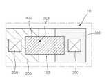
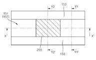
도 1 및 도 2는 본 출원의 일 예에 따른 비휘발성 메모리 소자의 1비트(bit) 단위 셀(unit cell)의 단면 형상 및 평면 레이아웃(layout) 형상을 보여준다.1 and 2 show a cross-sectional shape and a planar layout shape of a 1-bit unit cell of a nonvolatile memory device according to an example of the present application.
도 1 및 도 2를 참조하면, 본 출원에 따른 비휘발성 메모리 소자는, 반도체 기판(100) 표면에 돌출된 부분인 제1정션(junction)의 드레인 메사(drain mesa: 200)와, 기판(100)의 드레인 메사(200)와 이격된 부분에 위치하는 제2정션의 소스(source: 300), 드레인 메사(200)의 상면(201) 및 측면(203) 상에 중첩되고 소스(300) 상에 다다르게 연장된 플로팅 게이트(400), 플로팅 게이트(400)와 기판(100) 및 드레인 메사(200) 사이 계면에 도입된 유전층(500)을 포함하는 1비트 메모리 단위 셀(1bit memory unit cell: 10)을 구비할 수 있다. 단위 셀(10)은 전기적으로 프로그램(program) 및 이레이즈(erase) 동작을 수행하는 이이피롬(EEPROM) 셀로 구비될 수 있다.1 and 2, the nonvolatile memory device according to the present application includes a
드레인 메사(200)는 실리콘 기판과 같은 반도체 기판(100)의 표면 상에 돌출된 형상으로 제1정션 메사를 구비하고, 제1도전형의 불순물이 도핑(doping)된 제1불순물 영역으로 구비될 수 있다. 드레인 메사(200) 부분을 이루는 형상 부분 전체에 제1불순물 영역이 겹쳐지게 형성되거나, 또는 제1불순물 영역은 적어도 드레인 메사(200)의 표면부, 예컨대 상면(201) 및 측면(203) 부분의 표면부에 위치하도록 구비될 수 있다. 반도체 기판(100)에 구비된 웰(well: 101)의 제2도전형과 다른 제1도전형의 제1불순물 영역을 포함하여 드레인 메사(200)가 구비된다. 드레인 메사(200)와 이격된 반도체 기판(100) 표면부에 제1도전형의 불순물이 도핑된 제2불순물 영역으로 소스(300)가 구비될 수 있다. 동일한 웰(101) 내에 드레인 메사(200)와 소스(300)가 구비하므로, 셀 크기의 축소를 유도할 수 있다. 소스(300)와 드레인 메사(200) 사이의 이격 부분이 채널(channel) 영역(103)으로 구비될 수 있다. 드레인 메사(200)의 상면에 접촉하는 드레인 전극(250)과 소스(300)에 접촉하는 소스 전극(350)이 접속 단자로 구비될 수 있다.The
플로팅 게이트(400)는 단일층 폴리실리콘(polysilicon)층과 같은 단일층 게이트로 구비될 수 있다. 드레인 메사(200)에 인가되는 드레인 전압에 의해 플로팅 게이트(400)에 커플링(coupling)된 전압이 인가되어 프로그램 또는 읽기(read) 동작이 이루어지도록, 플로팅 게이트(400)가 드레인 메사(200)와 중첩되도록 구비될 수 있다. 플로팅 게이트(400)는 드레인 메사(200)의 상면(201) 일부에 겹쳐지고, 인접한 측면(203)에 겹쳐지게 연장되고, 채널 영역(103)에 겹쳐지게 연장되고, 또한, 채널 영역(103)에 인접하는 소스(300)의 일부 부분(301) 상에 겹쳐지게 연장되도록 구비될 수 있다. 드레인 메사(200)는 소스(300)를 구비한 반도체 기판(100)의 표면에 대해 돌출 또는 융기된 형상을 가지므로, 플로팅 게이트(400)와 겹쳐지는 정도가 드레인 메사(200)의 높이가 증가하는 정도에 따라 더 증가될 수 있다. 드레인 메사(200)의 높이가 높아지는 정도에 따라 측면(203)이 확장될 수 있으며, 측면(203)을 덮는 플로팅 게이트(400)의 부분 또한 확장될 수 있다.The
드레인 메사(200)는 반도체 기판(100)에 실질적으로 수직한 방향으로 플로팅 게이트(400)와 드레인이 중첩되는 폭 또는 면적을 확장시킬 수 있어, 드레인 메사(200)가 차지하는 반도체 기판(100)의 면적을 제한하면서도, 드레인과 플로팅 게이트(400)와의 중첩되는 폭 또는 면적을 증가시킬 수 있어, 드레인과 플로팅 게이트(400)와의 커플링 비(coupling ratio)를 증가시킬 수 있다. 드레인이 차지하는 영역의 크기를 실질적으로 축소할 수 있어, 비활성 메모리 소자의 메모리 셀(cell)을 크기를 축소할 수 있다.The
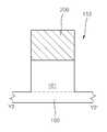
도 3은 1비트 단위 셀(10)에서 구현될 수 있는 커플링(coupling) 요소들을 보여준다. 도 3을 참조하면, 드레인 메사(200)의 상면(201) 부분과 이에 중첩된 플로팅 게이트(400) 부분에 제1커패시터(CA)가 이루어질 수 있으며, 드레인 메사(200)의 측면(203) 부분과 이에 중첩된 플로팅 게이트(400) 부분에 제2커패시터(CB)가 이루어질 수 있으며, 소스(300)와 이에 중첩된 플로팅 게이트(400) 부분에 제3커패시터(CB)가 구현될 수 있다. 도 2에 제시된 바와 같이 플로팅 게이트(400)가 장방형 평면 형상을 가져 그 폭이 각각의 부분에서 동일하다고 설정할 경우, 각각의 커패시터들의 커패시턴스는 중첩된 길이에 비례할 수 있다. 제1커패시터(CA)의 중첩 길이가 100 nm 이고, 제2커패시터(CB)의 중첩 길이가 1500Å이고, 제3커패시터(CC)의 중첩길이가 20 nm로 단위 셀(10)이 구비될 경우, 플로팅 게이트(400)에 대한 커플링 비(CR)는 (CA + CB)/ (CA + CB + CC)로서 92.6%로 얻어질 수 있다. 제2커패시터(CB)의 중첩 길이가 3500Å로 구비될 경우, 커플링 비는 95.7%로 증가될 수 있다.3 shows coupling elements that can be implemented in the 1-
이와 같이 고려된 두 경우 모두 드레인 메사(200) 형상을 도입하지 않고, 동일한 면적에서 평판형 플로팅 게이트를 구비한 경우에 비해 커플링 비를 현저하게 증가시킬 수 있다. 또한, 제2커패시터(CB)의 중첩 길이에 의존하여 커플링 비의 증가 정도를 조절할 수 있으므로, 드레인 메사(200)의 높이를 증가시켜 커플링 비를 보다 유효하게 증가시킬 수 있다. 즉, 드레인 메사(200)의 높이를 증가시켜 드레인과 플로팅 게이트(400)와의 중첩 면적을 증가시킴으로써 커플링 비를 증가시킬 수 있어 셀 크기 축소 효과를 구현할 수 있다.In both cases considered as described above, the coupling ratio can be significantly increased compared to the case where the
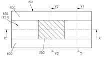
도 4 및 도 5는 본 출원의 일 예에 따른 비휘발성 메모리 소자의 2비트(bit) 트윈 셀(twin cell)의 단면 형상 및 평면 레이아웃(layout) 형상을 보여준다. 본 출원에 따른 비휘발성 메모리 소자는 도 1의 단위 셀(10) 형상이 우측 셀(11)과 좌측 셀(12)로 각각 구비되고, 우측 셀(11)과 좌측 셀(12)이 사이 가운데에 드레인 메사(200)를 공통으로 공유하여 하나의 트윈 셀(twin cell: 13)을 이룰 수 있다. 도 1의 단위 셀(10)은 예컨대 1비트의 데이터(data)를 메모리할 수 있다면, 도 2의 트윈 셀(13)은 하나의 드레인 메사(200)를 공유하면서 양측의 서로 구분되는 2개의 소스들(310, 320)로 2비트의 데이터를 메모리할 수 있다. 하나의 드레인 메사(200)를 공유하도록 트윈 셀(13: 11, 12)이 구비되므로, 셀의 크기를 보다 작게 축소할 수 있다.4 and 5 illustrate a cross-sectional shape and a planar layout shape of a 2-bit twin cell of a nonvolatile memory device according to an example of the present application. In the nonvolatile memory device according to the present application, the shape of the
트윈 셀(13)은 반도체 기판(100) 표면에 돌출된 부분인 제1정션 메사인 드레인 메사(200)와, 기판(100)의 드레인 메사(200)와 이격된 부분에 위치하는 제2정션의 제1소스( 310) 및 제2소스(320), 드레인 메사(200)의 상면 및 양측 측면들 상에 각각 중첩되고 소스들(310, 320) 상에 다다르게 각각 연장된 제1 및 제2플로팅 게이트들(410, 420), 제1플로팅 게이트(410)와 기판(100) 및 드레인 메사(200) 사이 계면에 도입된 제1유전층(510), 제2플로팅 게이트(420)와 기판(100) 및 드레인 메사(200) 사이 계면에 도입된 제2유전층(520)을 포함하여 2비트 메모리 동작을 할 수 있다. 트윈 셀(13)을 이루는 각각의 단위 셀들(11, 12)은 전기적으로 프로그램 및 이레이즈 동작을 수행하는 이이피롬(EEPROM) 셀로 구비될 수 있다.The
드레인 메사(200)는 실리콘 기판과 같은 반도체 기판(100)의 표면 상에 돌출된 형상으로, 제1도전형의 불순물이 도핑(doping)된 제1불순물 영역으로 구비될 수 있다. 드레인 메사(200) 부분을 이루는 형상 부분 전체에 제1불순물 영역이 겹쳐지게 형성되거나, 또는 제1불순물 영역은 적어도 드레인 메사(200)의 표면부, 예컨대 상면 및 측면 부분의 표면부에 위치하도록 구비될 수 있다. 반도체 기판(100)에 구비된 웰(101)의 제2도전형과 다른 제1도전형의 제1불순물 영역을 포함하여 드레인 메사(200)가 구비된다. 우측 셀(11)과 좌측 셀(12)은 웰(101)을 공유하도록 구비되며, 웰(101)의 공유에 의해 셀 크기 축소가 더 효과적으로 이루어질 수 있다.The
드레인 메사(200)와 이격된 반도체 기판(100) 표면부에 제1도전형의 불순물이 도핑된 제2불순물 영역으로 소스들(310, 320)이 구비될 수 있다. 소스(310, 320)와 드레인 메사(200) 사이의 이격 부분들이 각각 제1채널 영역(113) 및 제2채널 영역(123)으로 구비될 수 있다. 드레인 메사(200)의 상면에 접촉하는 공통 드레인 전극(250)과 제1 및 제2소스들(310, 320)에 각각 접촉하는 구분되는 제1 및 제2소스 전극들(351, 352)이 각각 접속 단자로 구비될 수 있다.
플로팅 게이트들(410, 420)은 단일층 폴리실리콘층과 같은 단일층 게이트로 구비될 수 있다. 드레인 메사(200)에 인가되는 드레인 전압에 의해 플로팅 게이트들(410, 420)에 커플링(coupling)된 전압이 인가되고, 제1 및 제2소스들(310, 320)에 각각 다른 소스 전압들이 인가되어, 각각의 단위 셀들(11, 12)에 대한 프로그램 또는 읽기(read) 동작이 독립적으로 이루어지도록, 플로팅 게이트들(410, 420)이 드레인 메사(200)와 중첩되도록 구비될 수 있다.The floating
플로팅 게이트들(410, 420)는 드레인 메사(200)의 상면 일부에 각각의 끝단부들이 상호 마주보도록 드레인 메사(200)의 상면 일부들에 각각 겹쳐지고, 인접한 측면들에 각각 겹쳐지게 연장되고, 채널 영역들(113, 123)에 각각 겹쳐지게 연장되고, 또한, 채널 영역들(113, 123)에 각각 인접하는 제1 및 제2소스들(310, 330)의 일부 부분들 상에 각각 겹쳐지게 연장되도록 구비될 수 있다. 드레인 메사(200)를 사이에 두고 양측으로 제1 및 제2플로팅 게이트들(410, 420)은 상호 대칭적으로 위치하고, 드레인 메사(200)를 사이에 두고 양측으로 제1 및 제2소스들(310, 320)은 상호 대칭적으로 위치한다.The floating
드레인 메사(200)는 소스들(310, 320)이 구비된 반도체 기판(100)의 표면에 대해 돌출 또는 융기된 형상을 가지므로, 플로팅 게이트들(410, 420)과 드레인 메사(200)가 겹쳐지는 부분의 크기 정도가 드레인 메사(200)의 높이가 증가하는 정도에 따라 더 증가될 수 있다. 드레인 메사(200)의 높이가 높아지는 정도에 따라 측면이 확장될 수 있으며, 측면을 덮는 플로팅 게이트들(410, 420)의 부분 또한 확장될 수 있다.Since the
드레인 메사(200)는 반도체 기판(100)에 실질적으로 수직한 방향으로 플로팅 게이트들(410, 420)와 드레인이 중첩되는 폭 또는 면적을 확장시킬 수 있어, 드레인 메사(200)가 차지하는 반도체 기판(100)의 면적을 제한하면서도, 드레인과 플로팅 게이트(410, 420)와의 중첩되는 폭 또는 면적을 증가시킬 수 있어, 드레인과 플로팅 게이트(410, 420)와의 커플링 비(coupling ratio)를 증가시킬 수 있다. 드레인이 차지하는 영역의 크기를 실질적으로 축소할 수 있어, 비활성 메모리 소자의 메모리 셀(cell)을 크기를 축소할 수 있다. 우측 셀(11) 및 좌측 셀(12) 각각은 도 3을 참조하여 설명한 바와 같이 커플링 비의 증가를 구현할 수 있어, 메모리 셀의 크기를 축소하는 효과를 유도할 수 있다.The
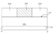
도 6은 트윈 셀의 구조를 포함하는 비휘발성 메모리 소자의 셀 어레이(cell array)의 일 예를 보여준다. 도 7은 도 6의 셀 어레이에 대응되는 등가 회로를 보여주는 도면이다. 도 6을 참조하면, 본 출원에 따른 비휘발성 메모리 소자는 기판(100) 표면에 돌출된 드레인 메사(200), 사이에 드레인 메사(200)를 두고 이격된 기판 부분들에 위치하는 제1 및 제2소스들(300), 및 드레인 메사(200)의 양측면들에 중첩되고 제1 및 제2소스(300) 상에 다다르는 제1 및 제2플로팅 게이트(400)들을 포함하여 행렬을 이루며 배치된 다수의 트윈 셀들(도 7의 13, 16, 19)의 어레이(array)를 포함한다. 개개의 트윈 셀들은 도 4 및 도 5에 제시된 바와 같이 드레인 메사(200)를 사이에 두고 제1 및 제2소스들(도 4의 310, 320)이 대칭적으로 배치되고, 제1 및 제2플로팅 게이트들(도 4의 410, 420)이 대칭적으로 구비될 수 있다.6 shows an example of a cell array of a nonvolatile memory device including a twin cell structure. 7 is a diagram illustrating an equivalent circuit corresponding to the cell array of FIG. 6. 6, the nonvolatile memory device according to the present application includes a
도 7을 참조하면, 행 방향으로 이웃하는 두 개의 트윈 셀(도 7의 13, 16)들은 도 6에 제시된 바와 같이 제1소스나 제2소스 중 어느 하나의 소스(300)를 상호 공통으로 공유하며 나란히 배치될 수 있다. 행을 이루며 배치된 트윈 셀(13, 16)들의 드레인 메사(200)들을 교번적으로 하나 건너 하나씩 공통되게 연결하는 BL<1>와 같은 제1비트 라인(bit line)과 BL<0>와 같은 제2비트 라인들(bit line)들이 교번적으로 반복 배치될 수 있다. 도 7에 제시된 바와 같이 비트 라인들은 BL<X>, BL<X-1>로 대표되는 두 개의 비트 라인들이 하나의 행 방향으로 이웃하게 배열 배치된 트윈 셀들의 드레인 메사(200)들에 교번적으로 연결되어 비트라인 디코더(B/L decoder)에 각각 연결된다. 행 방향으로 이웃하는 두 트윈 셀(13, 16)은 사이의 소스(300)를 공유하지만, 각각의 드레인 메사(200)들이 상호 구분되는 서로 다른 제1비트 라인인 BL<1> 및 제2비트 라인인 BL<0>에 접속되므로, 상호 독립적인 동작 수행이 가능하다.Referring to FIG. 7, two twin cells (13 and 16 of FIG. 7) adjacent to each other in a row direction share a
열을 이루며 배치된 트윈 셀들(13, 17)은 제1소스들을 상호 연결하는 SL<0>과 같은 제2소스 라인 및 제2소스들을 상호 연결하는 SL<1>과 같은 제1소스 라인들을 공유하도록 배치되고, 제1 및 제2소스 라인들이 반복 배치되어 소스 라인 디코더(S/L decoder)에 접속된다. 소스 라인 디코더와 비트 라인 디코더는 상호 직교되는 소스 라인들과 비트라인들이 각각 접속되도록 상호 직교되는 위치에 위치할 수 있다.The
도 6을 다시 참조하면, 어느 하나의 제1행(601)을 이루는 트윈 셀들은 하나의 웰(101)을 공유할 수 있다. 하나의 제1행(601)에 이웃하는 다른 제2행(602)을 이루는 트윈 셀들은 제1행(601)을 이루는 트윈 셀들과 얕은소자분리(STI)와 같은 소자분리층(600)에 의해 분리되도록 배치될 수 있다. 제1행(601)에 속하는 트윈 셀의 소스(300)인 제1소스와, 제2행(602)에 속하는 트윈 셀의 소스(300)인 제2소스 사이를 소자분리층(600)이 분리할 수 있으며, 이들 분리된 소스(300)들은 SL<X>와 같은 소스 라인에 공통되어 소스 라인 디코더에 접속될 수 있다. 소스(300)에 높은 전압이 인가될 경우 소자분리층(600)은 개개의 트윈 셀들을 분리하도록 연장될 수도 있다.Referring back to FIG. 6, twin cells forming any one
소자분리층(600)은 표면(610)이 실질적으로 드레인 메사(200)의 상면(201)과 대등한 표면 높이를 가질 수 있다. 소자분리층(600)은 제1행(601)을 이루는 트윈 셀들과 제2행(602)를 이루는 트윈 셀들이 서로 분리된 웰(101)들을 각각 공유하도록 웰(101)들을 분리하는 깊이로 반도체 기판(100) 내로 연장될 수 있다.The
도 7과 함께 도 4를 다시 참조하면, 본 출원에 따른 비휘발성 소자의 트윈 셀(11, 12)은 드레인 메사(200)에 공통으로 드레인 전압을 인가하는 드레인 전극(250)을 포함하고, 제1 및 제2소스들(310, 320)에 서로 다른 소스 전압을 인가하여 제1 및 제2플로팅 게이트들(410, 420)을 독립적으로 프로그램(program)시키거나 읽기(read) 또는 이레이즈(erase)하는 제 및 제2소스 전극들(351, 352)을 포함할 수 있다. 도 7과 같이 트윈 셀들(13, 16, 19)이 배열된 셀 어레이에서 트윈 셀들을 각각 구성하는 단위 셀들(11, 12) 또는 (14, 15) 또는 (17, 18)은, 도 8의 도표에 제시된 바와 같이 드레인 전극(250)과 소스 전극들(351, 352)에 인가되는 전압 조건들에 의해서 각각 독립적으로 동작될 수 있다.Referring again to FIG. 4 along with FIG. 7, the
도 8를 도 7 및 도 4와 함께 참조하면, 제1트윈 셀(13)의 좌측 단위 셀(12)을 프로그램하는 제1프로그램(PGM1) 동작은, BL<1>의 제1비트 라인을 통해 드레인 전극(250)이 접속된 드레인 메사(200)에 양의 프로그램전압(+Vpp)을 비트라인 전압(VBL) 또는 드레인 전압으로 인가하고, SL<0>의 제2소스 라인으로 제2소스 전극(352)이 접속된 제2소스(320)에 접지 전압 0V의 제2소스라인전압(VSL0)를 인가하고, SL<1>의 제1소스 라인으로 제1소스 전극(351)이 접속된 제1소스(310)을 플로팅(F)하는 제1소스라인전압(VSL1) 조건을 적용하고, 웰(101)에 접지 전압 OV를 인가하는 웰전압(Vwell)을 적용하여 이루어질 수 있다.Referring to FIG. 8 together with FIGS. 7 and 4, the first program PGM1 of programming the
제1프로그램(PGM1) 전압 조건에 의해서, 핫캐리어인젝션(HCI: Hot Carrier Injection) 방식으로 좌측 단위 셀(12)에 대한 프로그램이 이루어질 수 있다. 드레인을 통해 인가된 전압에 의해 커플링된 전압이 플로팅 게이트에 인가되고, 그 때 소스에 인가된 전압에 의해 발생된 핫 일렉트론(hot electron)이 플로팅 게이트에 트랩(trap)되는 방식으로 프로그램이 이루어질 수 있다. 예컨대, 드레인 메사(200)에 VBL로 인가된 +Vpp와 제2소스(320)에 VSL0로 접지하면, 커플링에 의해 제2플로팅 게이트(420)에 커플링된 전압이 인가되어 제2소스(320) 및 드레인 메사(200) 사이에 채널이 형성되고, 제2소스(320)와 드레인 메사(200) 사이에 형성된 전계에 의해 드레인 메사(200) 부근에 고 에너지 전자(hot electron)이 발생되고, 고 에너지 전자가 제2플로팅 게이트(420)로 주입될 수 있다.According to the voltage condition of the first program PGM1, a program for the
제1트윈 셀(13)의 우측 단위 셀(11)을 프로그램하는 제2프로그램(PGM2) 동작은, BL<1>의 제1비트 라인을 통해 드레인 전극(250)이 접속된 드레인 메사(200)에 양의 프로그램전압(+Vpp)를 비트라인 전압(VBL) 또는 드레인 전압으로 인가하고, SL<0>의 제2소스 라인으로 제2소스 전극(352)이 접속된 제2소스(320)에 플로팅(F)하는 제2소스라인전압(VSL0)을 적용하고, SL<1>의 제1소스 라인으로 제1소스 전극(351)이 접속된 제1소스(310)에 접지 전압 0V의 제1소스라인전압(VSL1) 조건을 적용하고, 웰(101)에 접지 전압 OV를 인가하는 웰전압(Vwell)을 적용하여 이루어질 수 있다.The second program (PGM2) of programming the
각각의 단위 셀(12, 11)을 이레이즈(erase)하는 동작은 파울러 노드하임 터널링(FN tunneling)으로 수행되며 상호 구분되어 상호 독립적으로 수행될 수 있다. 소스 바이어스(source bias)에 의해 플로팅 게이트와 소스 영역의 정션이 중첩된 영역에 강한 에너지(energy)를 가지게 된 홀(hole)dl 플로팅 게이트의 전압에 의해 플로팅 게이트로 주입될 수 있다. 예컨대 제1트윈 셀(13)의 좌측 단위 셀(12)을 이레이즈하는 제1이레이즈 (ERS1) 동작은, VBL로 0V 접지 전압을 인가하고, VSL0로 이레이즈전압(Vpp)를 인가하고, VSL1을 플로팅시키고, 웰(101)에 접지 전압 OV를 인가하는 웰전압(Vwell)을 적용하여 이루어질 수 있다. 제1트윈 셀(13)의 우측 단위 셀(11)을 이레이즈하는 제2이레이즈 (ERS1) 동작은, VBL로 0V 접지 전압을 인가하고, VSL0을 플로팅시키고 VSL1에 이레이즈전압(Vpp)를 인가하고, 웰(101)에 접지 전압 OV를 인가하는 웰전압(Vwell)을 적용하여 이루어질 수 있다.The operation of erasing each of the
읽기 동작은 드레인을 통해 인가된 읽기 전압 Vread를 통해 커플링된 전압이 플로팅 게이트에 인가되고, 드레인과 소스의 전압차에 의해 발생된 채널을 통해 읽기 동작이 이루어질 수 있다. 예컨대 좌측 단위 셀(12)에 대한 읽기 동작은, VBL에 읽기 전압 Vread를 인가하여 각각의 플로팅 게이트(420 410)들에 전압을 커플링하여 채널 형성을 유도하고, VSL1을 플로팅하고 VLS0에 소스 전압 Vss를 인가하여 좌측 셀(13)을 선택하여 읽기를 수행하도록 수행될 수 있다. 이때, Vss는 채널을 유도하기 위한 전압으로 드레인 메사(200)에 인가되는 Vread에 비해 작은 크기의 전압으로 인가될 수 있으며, 읽기 전압 Vread 는 Vpp로 인가될 수도 있다. 우측 단위 셀(11)에 대한 읽기 동작은, VBL에 읽기 전압 Vread를 인가하여 각각의 플로팅 게이트(420 410)들에 전압을 커플링하여 채널 형성을 유도하고, VSL0을 플로팅하고 VLS1에 소스 전압 Vss를 인가하여 우측 셀(11)을 선택하여 읽기를 수행하도록 수행될 수 있다.In the read operation, a voltage coupled through the read voltage Vread applied through the drain is applied to the floating gate, and the read operation may be performed through a channel generated by a voltage difference between the drain and the source. For example, in the read operation of the
상술한 바와 같은 전압 조건들을 적용하여, 하나의 제1트윈 셀(13) 내의 두 단위 셀들(12, 11)을 각각 독립적으로 선택하여 읽기, 프로그램 및 이레이즈 시킬 수 있다. 또한, 도 7에 제시된 바와 같이, 비트 라인(B/L<X>)을 선택하고 소스 라인(S/L<X>)을 선택하여 행 방향으로 이웃하는 제2트윈 셀(16)과 제1트윈 셀(13)을 구분하여 독립적으로 선택할 수 있고, 또한, 열 방향으로 이웃하는 제3트윈 셀(19)과 제1트윈 셀(13)을 구분하여 독립적으로 선택할 수 있다.By applying the voltage conditions as described above, two
도 4를 다시 참조하면, 본 출원에 따른 비휘발성 메모리 소자를 제조하는 방법은, 기판(100) 표면에 드레인 메사(200)를 돌출되도록 형성하고, 드레인 메사(200)의 양측면들에 각각 중첩되는 제1 및 제2플로팅 게이트들(410, 420)을 형성하고, 제1 및 제2플로팅 게이트들(410, 420) 각각에 인근하는 기판(100) 표면부에 제1 및 제2소스들(310, 320)을 형성하는 과정을 포함하여 수행될 수 있다. 제1 및 제2플로팅 게이트들(410, 420)은 드레인 메사(200)의 상면 일부분들에 중첩되어 상호 마주보도록 연장되도록 형성될 수 있다. 제1 및 제2플로팅 게이트들(410, 420)과 제1 및 제2소스들(310, 320)은 드레인 메사(200)를 사이에 두고 대칭적으로 위치하도록 형성될 수 있다.Referring again to FIG. 4, the method of manufacturing a nonvolatile memory device according to the present application includes forming the
도 9 내지 도 29는 비휘발성 메모리 소자를 형성하는 과정의 일 예를 보여준다.9 to 29 show an example of a process of forming a nonvolatile memory device.
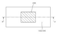
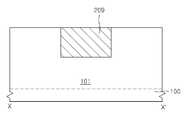
도 9는 반도체 기판(100)의 웰(101) 내에 형성한 제1불순물 영역(209)을 보여주고, 도 10은 도 9의 X-X' 절단선을 따르는 단면 형상을 보여준다. 웰(101)의 제2도전형과 다른 제1도전형의 불순물을 반도체 기판(100)에 도핑(doping)하여 제1불순물 영역(209)을 형성한다. 제1불순물 영역(209)은 제1정션으로 작용할 드레인 메사를 위한 영역을 형성될 수 있다.FIG. 9 shows a
도 11 및 도 12는 제1불순물 영역(209) 주위의 반도체 기판(100) 부분을 리세스(recess)하여 제1불순물 영역(209)을 제1정션의 드레인 메사(200)로 돌출시킨 형상을 보여준다. 제1불순물 영역(209) 주위의 반도체 기판(100) 부분을 선택적으로 식각 제거하여, 드레인 메사(200)의 측면을 노출하도록 제1리세스부(152)를 형성한다. 선택적 식각 과정을 적용하여 드레인 메사(200) 주위에 제1리세스부(152)를 리세스함으로써, 반도체 기판(100)의 리세스된 표면 상으로 드레인 메사(200)가 돌출된 형상이 유도되는 과정을 설명하지만, 드레인 메사(200)를 에피택셜 성장(epitaxial growth) 과정으로 선택적으로 성장시켜 돌출시킬 수도 있다.11 and 12 show a shape in which a portion of the
도 13은 드레인 메사(200)의 마주보는 두 측면들에 인접하는 부분에 소자분리를 위한 트렌치(trench: 153)들을 형성하는 과정을 보여주는 평면도이다. 도 14는 도 13의 X-X' 절단선을 따르는 단면 형상을 보여주고, 도 15는 도 13의 Y1-Y1' 절단선을 따르는 단면 형상을 보여주고, 도 16은 Y2-Y2' 절단선을 따르는 단면 형상을 보여준다. 드레인 메사(200)를 노출하는 제1리세스부(152)의 바닥 일부를 선택적으로 식각 제거하여 보다 깊은 깊이를 가지는 트렌치(153)들을 형성한다. 트렌치(153)는 반도체 기판(100)의 웰(101)의 바닥에 이르는 깊이로 형성되어, 웰(101)을 도 6에 제시된 바와 같이 트윈 셀들이 배열된 행들(601, 602)에 각각 속하는 독립된 분리 웰들로 분리되도록 유도할 수 있다. 트렌치(153)는 드레인 메사(200)의 측면에 인접하는 부분들에 위치하고, 트렌치(153)가 형성되지 않고 잔존하는 리세스부(152)의 바닥 표면부(151)는 소스 및 채널이 형성될 기판 표면부(151)로 설정될 수 있다. 제1리세스부(152)를 식각하고 다시 트렌치(153)를 식각하는 방식의 듀얼 얕은트렌치소자분리(dual STI) 과정을 예시하지만, 트렌치(153)를 먼저 식각하고 제1리세스부를 식각하는 과정으로 듀얼 STI 과정이 수행될 수도 있다. 트렌치(153)는 대략 제1리세스부(152)의 깊이에 비해 대략 2배 정도 또는 그 이상의 깊이를 가지도록 형성될 수 있다.13 is a plan view illustrating a process of forming
도 17은 트렌치(153)을 채우는 절연층(604)를 형성하는 과정을 보여주는 평면도이고, 도 18은 도 17의 X-X' 절단선을 따르는 단면 형상을 보여주고, 도 19는 도 17의 Y1-Y1' 절단선을 따르는 단면 형상을 보여준다. 트렌치(153)를 채우는 절연층(604)을 실리콘 산화물과 같은 유전 물질을 증착 또는 도포하여 형성한다. 이때, 절연층(604)은 트렌치(153)와 함께 제1리세스부(152)를 채우도록 형성될 수 있다. 절연층(604)의 증착 후 평탄화 과정을 수행하여 드레인 메사(200) 표면이 노출되도록 유도할 수 있다.FIG. 17 is a plan view showing a process of forming the insulating
도 20은 소자분리층(600)을 패터닝하는 과정을 보여주는 평면도이고, 도 21은 도 20의 X-X' 절단선을 따르는 단면 형상을 보여주고, 도 22는 도 20의 Y1-Y1' 절단선을 따르는 단면 형상을 보여주고, 도 23은 도 20의 Y2-Y2' 절단선을 따르는 단면 형상을 보여준다. 절연층(604)의 일부를 선택적으로 제거하여, 소스 및 채널이 형성될 기판 표면부(151)를 절연층이 제거된 노출 표면부(155)로 노출하도록 소자분리층(600)을 패터닝한다. 소자분리층(600)들 사이의 반도체 기판의 표면부(155)가 노출되도록 절연층(604)에 제2리세스부를 형성하는 식각 과정을 수행할 수 있다. 상술한 과정으로 소자분리층(600)들 사이에 드레인 메사(200)의 마주보는 양 측면들이 노출되는 구조가 형성될 수 있지만, 드레인 메사(200)를 위한 제1불순물 영역(도 10의 209) 양측으로 STI 소자분리층(600)들을 먼저 형성하고, 소자분리층(600)들 사이의 반도체 기판 부분을 선택적으로 식각 제거하여 리세스 부분을 형성함으로써, 드레인 메사(200)가 기판 표면부(155) 상측으로 돌출되도록 유도할 수도 있다.20 is a plan view showing a process of patterning the
도 24는 플로팅 게이트를 위한 층(401)을 형성하는 과정을 보여주고, 도 25은 도 24의 X-X' 절단선을 따르는 단면 형상을 보여준다. 드레인 메사(200) 및 노출된 표면부(155)를 덮는 플로팅 게이트를 위한 층(401)을 도전층, 예컨대, 폴리실리콘층을 증착하여 형성한다. 플로팅 게이트를 위한 층(401)을 형성하기 이전에 게이트 유전층으로 이용될 유전층(500)을 실리콘 산화물 등과 같은 유전 물질로 형성한다.FIG. 24 shows a process of forming a
도 26은 플로팅 게이트(400)를 패터닝하는 과정을 보여주고, 도 27은 도 26의 X-X' 절단선을 따르는 단면 형상을 보여준다. 플로팅 게이트의 층(401)의 일부 부분 및 유전층(500) 부분을 선택적으로 식각 제거하여 플로팅 게이트(400)를 형성한다. 플로팅 게이트(400) 및 유전층(500)은 드레인 전극이 접촉할 부분(207) 및 소스가 형성될 부분(307)을 노출하도록 패터닝될 수 있다.FIG. 26 shows a process of patterning the floating
도 28은 소스(300)를 형성하는 과정을 보여주고, 도 29는 도 28의 X-X' 절단선을 따르는 단면 형상을 보여준다. 플로팅 게이트(400)에 노출된 드레인 전극이 접촉할 부분(207) 및 소스가 형성될 부분(307)에 정션(junction) 형성을 위한 이온주입과 같은 불순물 도핑 과정을 수행한다. 이에 의해, 소스가 형성될 부분(307)에 제2불순물 영역으로 소스(300)가 형성된다. 이후에, 드레인 메사(200)에 접촉하는 드레인 전극(250) 및 정션 이온주입에 의해 형성된 소스(300)에 접촉하는 소스 전극(350)을 형성하여, 트윈 셀 구조의 비휘발성 메모리 소자를 구현한다.FIG. 28 shows a process of forming the
도 30 내지 도 37은 비휘발성 메모리 소자를 형성하는 과정의 다른 일 예를 보여준다.30 to 37 show another example of a process of forming a nonvolatile memory device.
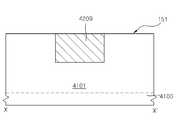
도 30은 소자분리를 위한 트렌치(trench: 4153)들을 형성하는 과정을 보여주는 평면도이다. 도 31은 도 30의 X-X' 절단선을 따르는 단면 형상을 보여주고, 도 32는 도 30의 Y-Y' 절단선을 따르는 단면 형상을 보여준다. 반도체 기판(4100)의 웰(4101)에 도핑된 제2도전형과 다른 제1도전형의 불순물을 반도체 기판(4100)에 도핑(doping)하여 제1불순물 영역(4209)을 형성한다. 제1불순물 영역(4209)은 제1정션으로 작용할 드레인 메사를 위한 영역으로 설정될 수 있다.30 is a plan view showing a process of forming
제1불순물 영역(4209)의 마주보는 두 측면들에 인접하는 반도체 기판(4200) 부분을 선택적으로 식각 제거하여, 소자분리를 위한 트렌치(4153)들을 형성한다. 두 트렌치(4153)들은 그 사이에 반도체 기판(4100)의 표면부(4151) 및 제1불순물 영역(4209)이 위치하도록 상호 간에 측 방향으로 나란히 마주보도록 형성될 수 있다. 트렌치(4153)의 측면으로 제1불순물 영역(4209)의 측면 부분 및 그 아래의 웰(4101)의 측면 부분이 노출될 수 있다. 트렌치(4153)가 형성되지 않고 잔존하는 반도체 기판(4100)의 표면부(4151)은 후속 과정에서 소스 및 채널이 위치할 영역으로 설정될 수 있다. 트렌치(4153)는 반도체 기판(4100)의 웰(4101)의 바닥에 이르는 깊이로 형성되어, 웰(4101)을 도 6에 제시된 바와 같이 트윈 셀들이 배열된 행들(601, 602)에 각각 속하는 독립된 분리된 웰들로 분리되도록 유도할 수 있다.A portion of the
도 33은 트렌치(4153)을 채우는 절연층(4604)를 형성하는 과정을 보여주는 평면도이고, 도 34는 도 33의 Y-Y' 절단선을 따르는 단면 형상을 보여준다. 트렌치(4153)를 채우는 절연층(4604)을 실리콘 산화물과 같은 유전 물질을 증착 또는 도포하여 형성한다. 이때, 절연층(4604)이 트렌치(4153)를 채우고 표면부(4151)를 덮도록 연장될 수 있으므로, 절연층(4604)의 증착 후 평탄화 과정, 예컨대, CMP(Chemical Mechanical Polishing)나 에치 백(etch back) 과정을 수행하여 표면부(4151)와 제1불순물 영역(4209)의 표면이 노출되도록 유도할 수 있다. 이러한 평탄화 과정으로 절연층(4604)이 트렌치(4153)을 채우는 형상의 소자분리층으로 패터닝된다. 제1불순물 영역(4209)를 형성하는 도핑 과정은 소자분리 절연층(4604)를 형성한 이후에 수행될 수도 있다.33 is a plan view showing a process of forming the insulating
도 35는 드레인 메사(4200)를 패터닝하는 과정을 보여주는 평면도이고, 도 36은 도 35의 X-X' 절단선을 따르는 단면 형상을 보여준다. 제1불순물 영역(209) 주위의 반도체 기판(4100)의 표면부(도 33의 4151) 부분을 리세스(recess)하여 제1불순물 영역(도 33의 4209)을 제1정션의 드레인 메사(4200)로 돌출시킨다. 제1불순물 영역(4209)을 선택적으로 차폐하는 식각 마스크(etch mask: 도시되지 않음)를 이용하여 표면부(4151)를 선택적으로 식각 제거하여 리세스부(4155)를 형성할 수 있다. 두 리세스부(4155)들은 사이에 제1불순물 영역(4209)이 잔존하여 드레인 메사(4200)로 돌출되도록 형성될 수 있다. 리세스부(4155)는 트렌치(도 32의 4153) 보다 얕은 깊이를 가질 수 있고, 제1불순물 영역(4209)의 다른 측면을 노출하도록 형성될 수 있다. 리세스부(4155)의 바닥부(4152)는 채널 및 소스가 형성될 위치를 제공한다. 리세스부(4155)를 형성하는 식각 과정과 트렌치(도 32의 4153)를 형성하는 식각 과정으로 제1불순물 영역(4209)가 리세스부(4155)의 바닥부(4152) 보다 높게 돌출되는 형상으로 패터닝되어 드레인 메사(4200)가 설정된다.FIG. 35 is a plan view showing a process of patterning the
도 37은 플로팅 게이트(4400)을 형성하는 과정을 보여준다. 드레인 메사(4200) 및 리세스부(4155)의 바닥부(4152)를 덮는 게이트 유전층(4500)을 형성하고, 그 상에 플로팅 게이트(4400)를 위한 층을 형성한다. 플로팅 게이트(4400) 및 유전층(4500)은 드레인 전극이 접촉할 부분 및 제2불순물 영역의 소스(4300)가 형성될 부분을 노출하도록 패터닝될 수 있다.37 shows a process of forming the floating
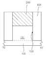
도 38은 비휘발성 메모리 소자의 다른 일례를 보여준다. 비휘발성 메모리 소자는 제1트윈 셀(2013)과 제2트윈 셀(2015)이 사이에 소자분리층(2600)을 두고 배치된 셀 어레이를 포함한다. 제1트윈 셀(2013)은 기판(2100) 표면에 돌출된 제1드레인 메사(2201)와, 이를 사이에 상호 이격된 기판(2100) 부분들에 각각 위치하는 제1소스(2301)와 제2소스(2305), 및 제1드레인 메사(2201)의 양측면들에 중첩되고 제1소스 및 제2소스들(2301, 2305) 상에 다다르는 제1 및 제2플로팅 게이트들(2401, 2405)들을 포함할 수 있다. 제1드레인 메사(2201)에 접속되는 제1드레인 전극(2251)과, 제1소스 및 제2소스들(2301, 2305) 각각에 접속되는 제1 및 제2소스 전극들(2351, 2355)를 더 포함할 수 있다.38 shows another example of a nonvolatile memory device. The nonvolatile memory device includes a cell array in which the
제2트윈 셀(2015)은 기판(2100) 표면에 돌출된 제2드레인 메사(2203)와, 이를 사이에 상호 이격된 기판(2100) 부분들에 각각 위치하는 제3소스(2303)와 제4소스(2307), 및 제2드레인 메사(2201)의 양측면들에 중첩되고 제3소스 및 제4소스들(2303, 2307) 상에 다다르는 제3 및 제4플로팅 게이트들(2403, 2407)들을 포함할 수 있다. 제2드레인 메사(2203)에 접속되는 제2드레인 전극(2253)과, 제3소스 및 제4소스들(2303, 2307) 각각에 접속되는 제3 및 제4소스 전극들(2353, 2357)를 더 포함할 수 있다.The second
소자분리층(2600)은 트윈 셀들(2013, 2015) 사이를 분리하도록 위치하며, 제1트윈 셀(2013)의 제1소스(2301)과 이웃하는 제2트윈 셀((2015)의 제3소스(2303) 사이를 분리하도록 위치할 수 있다. 이때, 소자분리층(2600)은 웰(2101)들이 각각 제1 및 제2트윈 셀들(2013, 2015)들에 속하는 부분들로 분리되도록 깊게 형성될 수 있다. 소자분리층(2600)의해 분리된 제1소스(2301)와 제3소스(2303)에 공통되지 않고 상호 독립적으로 소스 전압이 인가될 수 있다. 제1소스(2301)와 제3소스(2303)가 상호 독립적이므로, 제1드레인 메사(2201)에 접속되는 제1드레인 전극(2251)과 제2드레인 메사(2203)에 접속되는 제2드레인 전극(2253)이 상호 간에 공통되도록 연결되어도, 제1플로팅 게이트(2401)와 제3플로팅 게이트(2403)에 독립적으로 프로그램, 이레이즈 및 읽기 동작을 수행할 수 있다. 따라서, 하나의 비트 라인에 이웃하는 두 개의 트윈 셀들(2013, 2015)가 공통으로 접속될 수 있다.The
상술한 바와 같이 본 출원의 실시 형태들을 도면들을 예시하며 설명하지만, 이는 본 출원에서 제시하고자 하는 바를 설명하기 위한 것이며, 세밀하게 제시된 형상으로 본 출원에서 제시하고자 하는 바를 한정하고자 한 것은 아니다. 본 출원에서 제시한 기술적 사상이 반영되는 한 다양한 다른 변형예들이 가능할 것이다.As described above, embodiments of the present application are illustrated and described with drawings, but this is for explaining what is to be presented in the present application, and is not intended to limit what is to be presented in the present application in a detailed shape. As long as the technical idea presented in the present application is reflected, various other modifications will be possible.
100: 반도체 기판, 200: 드레인 메사,
300: 소스,400: 플로팅 게이트.
100: semiconductor substrate, 200: drain mesa,
300: source, 400: floating gate.
Claims (32)
Translated fromKorean사이에 상기 드레인 메사를 두고 이격된 상기 기판 부분들에 위치하는 제1 및 제2소스(source)들; 및
상기 드레인 메사의 양측면들에 중첩되고 상기 제1 및 제2소스 상에 다다르는 제1 및 제2플로팅 게이트(floating gate)들;을 포함하는 비휘발성 메모리 소자.A drain mesa protruding from the substrate surface;
First and second sources positioned on portions of the substrate spaced apart from each other with the drain mesa therebetween; And
And first and second floating gates overlapping both sides of the drain mesa and reaching the first and second sources.
상기 제1 및 제2플로팅 게이트들은
상기 드레인 메사의 상면 일부분들에 중첩되어 상호 마주보도록 연장된 비휘발성 메모리 소자.The method of claim 5,
The first and second floating gates are
A nonvolatile memory device extending to face each other by overlapping portions of the upper surface of the drain mesa.
상기 제1 및 제2플로팅 게이트들 사이의 상기 드레인 메사의 상면 부분에 접촉하는 공통 드레인 전극; 및
상기 제1 및 제2소스들에 각각 접촉하는 제1 및 제2소스 전극들을 더 포함하는 비휘발성 메모리 소자.The method of claim 6,
A common drain electrode contacting an upper surface portion of the drain mesa between the first and second floating gates; And
A nonvolatile memory device further comprising first and second source electrodes contacting the first and second sources, respectively.
상기 제1 및 제2플로팅 게이트들과 상기 제1 및 제2소스들은
상기 드레인 메사를 사이에 두고 대칭적으로 위치하는 비휘발성 메모리 소자.The method of claim 5,
The first and second floating gates and the first and second sources are
Nonvolatile memory devices symmetrically positioned with the drain mesa interposed therebetween.
상기 드레인 메사는 상기 양측면 및 상면 부분에 형성된 제1불순물 영역을 포함하고,
상기 제1 및 제2소스들은 각각 상기 기판 표면 부분에 형성된 제2불순물 영역들을 포함하는 비휘발성 메모리 소자.The method of claim 5,
The drain mesa includes first impurity regions formed on both side surfaces and upper surface portions,
Each of the first and second sources includes second impurity regions formed on a surface portion of the substrate.
상기 열을 이루며 배치된 트윈 셀들의 상기 제1소스들 및 상기 제2소스들을 각각 연결하는 제1 및 제2소스 라인들; 및
상기 행을 이루며 배치된 트윈 셀들의 상기 드레인 메사들을 교번적으로 하나 건너 하나씩 공통되게 연결하는 제1 및 제2비트 라인(bit line)들;을 포함하는 비휘발성 메모리 소자.A drain mesa protruding from the surface of the substrate, first and second sources positioned on portions of the substrate spaced apart from each other with the drain mesa therebetween, and overlapping on both sides of the drain mesa and the A plurality of twin cells arranged in a matrix including first and second floating gates reaching on the first and second sources;
First and second source lines respectively connecting the first sources and the second sources of the twin cells arranged in the row; And
And first and second bit lines alternately connecting the drain mesas of the twin cells arranged in the row to one another in common.
상기 행을 이루며 배치된 트윈 셀들 중 이웃하는 둘의 트윈 셀들은
사이의 상기 제1소스 또는 상기 제2소스를 공통으로 공유하는 비휘발성 메모리 소자.The method of claim 10,
Among the twin cells arranged in the row, two adjacent twin cells are
A nonvolatile memory device that shares the first source or the second source in common.
상기 제1소스를 공통으로 공유하는 이웃하는 두 트윈 셀들은
각각 상기 제1비트 라인 및 제2비트 라인에 접속되는 비휘발성 메모리 소자.The method of claim 11,
Two neighboring twin cells that share the first source in common
Nonvolatile memory devices connected to the first bit line and the second bit line, respectively.
상기 트윈 셀들은
상호 간에 웰(well)을 공유하는 비휘발성 메모리 소자.The method of claim 10,
The twin cells are
Nonvolatile memory devices that share wells with each other.
어느 하나의 상기 행을 이루며 배치된 트윈 셀들과
이웃하는 다른 행을 이루며 배치된 트윈 셀들 사이를 분리하며
상기 기판에 형성된 소자분리층을 더 포함하는 비휘발성 메모리 소자.The method of claim 10,
Twin cells arranged in any one of the above rows and
Separating between twin cells placed in different neighboring rows
A nonvolatile memory device further comprising a device isolation layer formed on the substrate.
상기 소자분리층은
상기 분리된 행들을 각각 이루는 트윈 셀들이
서로 분리된 웰(well)들을 각각 공유하도록 상기 웰을 분리하는 비휘발성 메모리 소자.The method of claim 14,
The device isolation layer is
Twin cells forming each of the separated rows
A nonvolatile memory device for separating the wells so as to share separated wells from each other.
상기 제1 및 제2플로팅 게이트들은
상기 드레인 메사의 상면 일부분들에 중첩되어 상호 마주보도록 연장된 비휘발성 메모리 소자.The method of claim 10,
The first and second floating gates are
A nonvolatile memory device extending to face each other by overlapping portions of the upper surface of the drain mesa.
상기 제1 및 제2플로팅 게이트들 사이의 상기 드레인 메사의 상면 부분에 접촉하는 공통 드레인 전극; 및
상기 제1 및 제2소스들에 각각 접촉하는 제1 및 제2소스 전극들을 더 포함하는 비휘발성 메모리 소자.The method of claim 16,
A common drain electrode contacting an upper surface portion of the drain mesa between the first and second floating gates; And
A nonvolatile memory device further comprising first and second source electrodes contacting the first and second sources, respectively.
상기 제1 및 제2플로팅 게이트들과 상기 제1 및 제2소스들은
상기 드레인 메사를 사이에 두고 대칭적으로 위치하는 비휘발성 메모리 소자.The method of claim 10,
The first and second floating gates and the first and second sources are
Nonvolatile memory devices symmetrically positioned with the drain mesa interposed therebetween.
상기 드레인 메사는 상기 양측면 및 상면 부분에 형성된 제1불순물 영역을 포함하고,
상기 제1 및 제2소스들은 각각 상기 기판 표면 부분에 형성된 제2불순물 영역들을 포함하는 비휘발성 메모리 소자.The method of claim 10,
The drain mesa includes first impurity regions formed on both side surfaces and upper surface portions,
Each of the first and second sources includes second impurity regions formed on a surface portion of the substrate.
상기 어느 하나의 트윈 셀의 상기 제1소스와 이웃하는 다른 하나의 트윈 셀의 상기 제2소스 사이를 분리하는 소자분리층;을 포함하는 비휘발성 메모리 소자.A drain mesa protruding from the surface of the substrate, first and second sources positioned on portions of the substrate spaced apart from each other with the drain mesa therebetween, and overlapping on both sides of the drain mesa and the A plurality of twin cells including first and second floating gates reaching on the first and second sources; And
And a device isolation layer separating between the first source of one of the twin cells and the second source of another adjacent twin cell.
상기 소자분리층은
양측에 배치된 상기 트윈 셀들이 서로 분리된 웰(well)들을 포함하도록 상기 웰들을 분리하는 비휘발성 메모리 소자.The method of claim 20,
The device isolation layer is
A nonvolatile memory device for separating the wells so that the twin cells disposed on both sides include wells separated from each other.
사이에 상기 드레인 메사를 두고 이격된 제1 및 제2소스들; 및
상기 드레인 메사의 상면 일부 및 양측면들에 각각 중첩되고 상기 제1 및 제2소스에 각각 다다르게 연장된 제1 및 제2플로팅 게이트들;을 포함하는 비휘발성 메모리 소자이고,
상기 드레인 메사에 공통으로 드레인 전압을 인가하는 드레인 전극; 및
상기 제1 및 제2소스들에 서로 다른 소스 전압을 인가하여
상기 제1 및 제2플로팅 게이트들을 독립적으로 프로그램(program)시키거나 읽기(read) 또는 이레이즈(erase)하는 제 및 제2소스 전극들을 포함하는 비휘발성 메모리 소자.Drain meas protruding from the substrate surface;
First and second sources spaced apart from each other with the drain mesa therebetween; And
A nonvolatile memory device including first and second floating gates respectively overlapping on a portion of an upper surface and both side surfaces of the drain mesa and extending to the first and second sources, respectively,
A drain electrode for applying a drain voltage in common to the drain mesa; And
By applying different source voltages to the first and second sources
A nonvolatile memory device comprising first and second source electrodes for independently programming, reading, or erasing the first and second floating gates.
상기 드레인 메사의 양측면들에 각각 중첩되는 제1 및 제2플로팅 게이트들을 형성하는 단계; 및
상기 제1 및 제2플로팅 게이트들 각각에 인근하는 상기 기판 표면부에 제1 및 제2소스들을 형성하는 단계;를 포함하는 비휘발성 메모리 소자 제조 방법.Forming a drain mesa to protrude from the surface of the substrate;
Forming first and second floating gates respectively overlapping on both sides of the drain mesa; And
Forming first and second sources on the surface of the substrate adjacent to each of the first and second floating gates.
상기 제1 및 제2플로팅 게이트들은
상기 드레인 메사의 상면 일부분들에 중첩되어 상호 마주보도록 연장되도록 형성되는 비휘발성 메모리 소자 제조 방법.The method of claim 23,
The first and second floating gates are
A method of manufacturing a nonvolatile memory device that is formed to extend to face each other by overlapping portions of the upper surface of the drain mesa.
상기 제1 및 제2플로팅 게이트들과 상기 제1 및 제2소스들은
상기 드레인 메사를 사이에 두고 대칭적으로 위치하도록 형성되는 비휘발성 메모리 소자 제조 방법.The method of claim 23,
The first and second floating gates and the first and second sources are
A method of manufacturing a nonvolatile memory device formed to be symmetrically positioned with the drain mesa interposed therebetween.
상기 드레인 메사의 상기 양측면 및 상면 부분에 위치하는 제1불순물 영역을 형성하는 단계; 및
상기 기판 표면 부분에 상기 제1 및 제2소스들을 제공하는 제2불순물 영역들을 형성하는 단계를 더 포함하는 비휘발성 메모리 소자 제조 방법.The method of claim 23,
Forming first impurity regions located on both side and upper surfaces of the drain mesa; And
The method of manufacturing a nonvolatile memory device further comprising forming second impurity regions providing the first and second sources on the surface of the substrate.
상기 트렌치를 채우는 소자분리층을 형성하는 단계;
상기 드레인 메사의 양측면들에 각각 중첩되는 제1 및 제2플로팅 게이트들을 형성하는 단계; 및
상기 제1 및 제2플로팅 게이트들 각각에 인근하는 상기 리세스부의 표면부에 제1 및 제2소스들을 형성하는 단계;를 포함하는 비휘발성 메모리 소자 제조 방법.Forming a recess portion protruding a drain mesa on the substrate surface and a trench positioned at a bottom portion of the recess portion;
Forming an isolation layer filling the trench;
Forming first and second floating gates respectively overlapping on both sides of the drain mesa; And
And forming first and second sources on a surface portion of the recess portion adjacent to each of the first and second floating gates.
상기 리세스부를 형성하는 단계 이전에
상기 드레인 메사(mesa)로 돌출될 상기 기판 부분에 불순물 영역을 도핑(doping)하는 단계를 더 포함하는 비휘발성 메모리 소자 제조 방법.The method of claim 27,
Before the step of forming the recess
The method of manufacturing a nonvolatile memory device further comprising the step of doping an impurity region on a portion of the substrate that will protrude through the drain mesa.
상기 리세스부 바닥을 형성하는 단계는
상기 드레인 메사(mesa) 주위의 상기 기판 부분을 선택적으로 식각 제거하는 단계를 더 포함하는 비휘발성 메모리 소자 제조 방법.The method of claim 27,
Forming the bottom of the recess portion
The method of manufacturing a nonvolatile memory device further comprising the step of selectively etching and removing a portion of the substrate around the drain mesa.
상기 트렌치를 형성하는 단계는
상기 드레인 메사(mesa)의 마주보는 두 측면에 인접하는 상기 리세스부의 바닥 부분을 선택적으로 식각 제거하는 단계를 포함하는 비휘발성 메모리 소자 제조 방법.The method of claim 29,
The step of forming the trench
And selectively etching and removing bottom portions of the recess portions adjacent to two opposite sides of the drain mesa.
상기 트렌치들을 각각 채우는 소자분리층들을 형성하는 단계;
상기 소자분리층들 사이의 상기 기판의 일 부분들을 선택적으로 제거하여 사이에 드레인 메사(drain mesa)가 돌출된 형상으로 잔존시키는 리세스(recess)부들을 형성하는 단계;
상기 드레인 메사의 양측면들에 각각 중첩되는 제1 및 제2플로팅 게이트들을 형성하는 단계; 및
상기 제1 및 제2플로팅 게이트들 각각에 인근하는 상기 리세스부의 바닥부에 제1 및 제2소스들을 형성하는 단계;를 포함하는 비휘발성 메모리 소자 제조 방법.Forming trenches side by side in the substrate surface;
Forming device isolation layers filling each of the trenches;
Selectively removing portions of the substrate between the device isolation layers to form recess portions in which a drain mesa protrudes therebetween;
Forming first and second floating gates respectively overlapping on both sides of the drain mesa; And
And forming first and second sources at the bottom of the recess portion adjacent to each of the first and second floating gates.
상기 리세스부를 형성하는 단계 이전에
상기 드레인 메사(mesa)로 돌출될 상기 기판 부분에 불순물 영역을 도핑(doping)하는 단계를 더 포함하는 비휘발성 메모리 소자 제조 방법.
The method of claim 31,
Before the step of forming the recess
The method of manufacturing a nonvolatile memory device further comprising the step of doping an impurity region on a portion of the substrate that will protrude through the drain mesa.
Priority Applications (5)
| Application Number | Priority Date | Filing Date | Title |
|---|---|---|---|
| KR1020140033655AKR102142155B1 (en) | 2014-03-21 | 2014-03-21 | Non-volatile memory device with single layered floating gate and fabricating method for the same |
| US14/470,652US9318497B2 (en) | 2014-03-21 | 2014-08-27 | Nonvolatile memory devices having single-layered floating gates |
| TW103129823ATWI622160B (en) | 2014-03-21 | 2014-08-29 | Non-volatile memory device with single-layer floating gate |
| CN201410524481.6ACN104934432B (en) | 2014-03-21 | 2014-10-08 | Nonvolatile memory device with single-layer floating gate |
| US15/069,282US9634102B2 (en) | 2014-03-21 | 2016-03-14 | Nonvolatile memory devices having single-layered floating gates |
Applications Claiming Priority (1)
| Application Number | Priority Date | Filing Date | Title |
|---|---|---|---|
| KR1020140033655AKR102142155B1 (en) | 2014-03-21 | 2014-03-21 | Non-volatile memory device with single layered floating gate and fabricating method for the same |
Publications (2)
| Publication Number | Publication Date |
|---|---|
| KR20150110964A KR20150110964A (en) | 2015-10-05 |
| KR102142155B1true KR102142155B1 (en) | 2020-08-10 |
Family
ID=54121522
Family Applications (1)
| Application Number | Title | Priority Date | Filing Date |
|---|---|---|---|
| KR1020140033655AActiveKR102142155B1 (en) | 2014-03-21 | 2014-03-21 | Non-volatile memory device with single layered floating gate and fabricating method for the same |
Country Status (4)
| Country | Link |
|---|---|
| US (2) | US9318497B2 (en) |
| KR (1) | KR102142155B1 (en) |
| CN (1) | CN104934432B (en) |
| TW (1) | TWI622160B (en) |
Families Citing this family (4)
| Publication number | Priority date | Publication date | Assignee | Title |
|---|---|---|---|---|
| US9972493B2 (en)* | 2016-08-08 | 2018-05-15 | Silicon Storage Technology, Inc. | Method of forming low height split gate memory cells |
| TWI709227B (en)* | 2017-04-10 | 2020-11-01 | 聯華電子股份有限公司 | Non-volatile memory device and operation method thereof |
| WO2024084438A1 (en)* | 2022-10-20 | 2024-04-25 | King Abdullah University Of Science And Technology | Ga2O3 BASED NONVOLATILE FLASH MEMORY FOR OXIDE ELECTRONICS AND METHOD |
| US20240258373A1 (en)* | 2023-02-01 | 2024-08-01 | Taiwan Semiconductor Manufacturing Company, Ltd. | Transistor device having a gate setback from a gate dielectric |
Citations (4)
| Publication number | Priority date | Publication date | Assignee | Title |
|---|---|---|---|---|
| US5338953A (en) | 1991-06-20 | 1994-08-16 | Mitsubishi Denki Kabushiki Kaisha | Electrically erasable and programmable semiconductor memory device with trench memory transistor and manufacturing method of the same |
| KR100221062B1 (en) | 1993-11-08 | 1999-09-15 | 마찌다 가쯔히꼬 | A flash memory and manufacturing method of the same |
| US6998670B2 (en) | 2003-04-25 | 2006-02-14 | Atmel Corporation | Twin EEPROM memory transistors with subsurface stepped floating gates |
| JP2006140518A (en) | 2000-07-03 | 2006-06-01 | Matsushita Electric Ind Co Ltd | Nonvolatile semiconductor memory device |
Family Cites Families (7)
| Publication number | Priority date | Publication date | Assignee | Title |
|---|---|---|---|---|
| US5008212A (en)* | 1988-12-12 | 1991-04-16 | Chen Teh Yi J | Selective asperity definition technique suitable for use in fabricating floating-gate transistor |
| JP2630252B2 (en)* | 1994-04-26 | 1997-07-16 | 日本電気株式会社 | Tunnel transistor and manufacturing method thereof |
| TW425660B (en)* | 1997-12-12 | 2001-03-11 | Mosel Vitelic Inc | Method of forming uniform dielectric layer between two conductive layers in integrated circuit |
| KR100494152B1 (en) | 2002-12-30 | 2005-06-13 | 매그나칩 반도체 유한회사 | High density single poly eeprom |
| KR20060094379A (en)* | 2005-02-24 | 2006-08-29 | 삼성전자주식회사 | Morse transistor having a protruding source / drain structure and its manufacturing method |
| KR100780866B1 (en)* | 2006-12-14 | 2007-11-30 | 삼성전자주식회사 | Nonvolatile Memory Device and Formation Method |
| JP2011134981A (en)* | 2009-12-25 | 2011-07-07 | Sanyo Electric Co Ltd | Non-volatile semiconductor storage device and method of manufacturing the same |
- 2014
- 2014-03-21KRKR1020140033655Apatent/KR102142155B1/enactiveActive
- 2014-08-27USUS14/470,652patent/US9318497B2/enactiveActive
- 2014-08-29TWTW103129823Apatent/TWI622160B/enactive
- 2014-10-08CNCN201410524481.6Apatent/CN104934432B/enactiveActive
- 2016
- 2016-03-14USUS15/069,282patent/US9634102B2/enactiveActive
Patent Citations (4)
| Publication number | Priority date | Publication date | Assignee | Title |
|---|---|---|---|---|
| US5338953A (en) | 1991-06-20 | 1994-08-16 | Mitsubishi Denki Kabushiki Kaisha | Electrically erasable and programmable semiconductor memory device with trench memory transistor and manufacturing method of the same |
| KR100221062B1 (en) | 1993-11-08 | 1999-09-15 | 마찌다 가쯔히꼬 | A flash memory and manufacturing method of the same |
| JP2006140518A (en) | 2000-07-03 | 2006-06-01 | Matsushita Electric Ind Co Ltd | Nonvolatile semiconductor memory device |
| US6998670B2 (en) | 2003-04-25 | 2006-02-14 | Atmel Corporation | Twin EEPROM memory transistors with subsurface stepped floating gates |
Also Published As
| Publication number | Publication date |
|---|---|
| CN104934432B (en) | 2019-05-07 |
| US9634102B2 (en) | 2017-04-25 |
| US20160197153A1 (en) | 2016-07-07 |
| TW201537725A (en) | 2015-10-01 |
| US9318497B2 (en) | 2016-04-19 |
| CN104934432A (en) | 2015-09-23 |
| US20150270360A1 (en) | 2015-09-24 |
| TWI622160B (en) | 2018-04-21 |
| KR20150110964A (en) | 2015-10-05 |
Similar Documents
| Publication | Publication Date | Title |
|---|---|---|
| US9286988B2 (en) | Nonvolatile memory device and operating method thereof | |
| US9219134B2 (en) | Semiconductor device and method of manufacturing the same | |
| KR101480286B1 (en) | Highly integrated semiconductor device and manufacturing method thereof | |
| US9761606B1 (en) | Stacked non-volatile semiconductor memory device with buried source line and method of manufacture | |
| JP6503077B2 (en) | High density split gate memory cell | |
| CN114335186B (en) | Split gate non-volatile memory cell with erase gate disposed above word line gate and method of making the same | |
| KR102119335B1 (en) | Reduced size isolated gate non-volatile flash memory cell and method of manufacturing same | |
| KR20130072076A (en) | Nonvolatile memory device and method for fabricating the same | |
| KR102763644B1 (en) | Split gate, 2-bit nonvolatile memory cell having an erase gate arranged over a word line gate, and method for manufacturing the same | |
| CN104218075A (en) | Semiconductor device and method for manufacturing semiconductor device | |
| KR102142155B1 (en) | Non-volatile memory device with single layered floating gate and fabricating method for the same | |
| JP2021106298A (en) | Manufacturing method for semiconductor memory | |
| KR101073640B1 (en) | High-density vertical-type semiconductor memory cell string, cell string array and fabricating method thereof | |
| JP2003045981A (en) | Semiconductor device | |
| US6972456B2 (en) | Semiconductor device and method of fabricating the same | |
| JP2003045980A (en) | Semiconductor device | |
| JP2011054658A (en) | Nonvolatile semiconductor memory device | |
| JP2011066038A (en) | Semiconductor memory device | |
| CN102347371A (en) | Nonvolatile semiconductor memory transistor and method for manufacturing nonvolatile semiconductor memory | |
| KR102075004B1 (en) | Nonvolatile memory device | |
| US20040072403A1 (en) | Method of manufacturing semiconductor device | |
| JP2014236015A (en) | Semiconductor device, and method of manufacturing the same | |
| KR20080079010A (en) | Multi-bit flash memory cell, driving method thereof and manufacturing method thereof |
Legal Events
| Date | Code | Title | Description |
|---|---|---|---|
| PA0109 | Patent application | Patent event code:PA01091R01D Comment text:Patent Application Patent event date:20140321 | |
| PG1501 | Laying open of application | ||
| A201 | Request for examination | ||
| PA0201 | Request for examination | Patent event code:PA02012R01D Patent event date:20190211 Comment text:Request for Examination of Application Patent event code:PA02011R01I Patent event date:20140321 Comment text:Patent Application | |
| E902 | Notification of reason for refusal | ||
| PE0902 | Notice of grounds for rejection | Comment text:Notification of reason for refusal Patent event date:20200113 Patent event code:PE09021S01D | |
| E701 | Decision to grant or registration of patent right | ||
| PE0701 | Decision of registration | Patent event code:PE07011S01D Comment text:Decision to Grant Registration Patent event date:20200727 | |
| PR0701 | Registration of establishment | Comment text:Registration of Establishment Patent event date:20200731 Patent event code:PR07011E01D | |
| PR1002 | Payment of registration fee | Payment date:20200803 End annual number:3 Start annual number:1 | |
| PG1601 | Publication of registration | ||
| PR1001 | Payment of annual fee | Payment date:20230626 Start annual number:4 End annual number:4 | |
| PR1001 | Payment of annual fee | Payment date:20240625 Start annual number:5 End annual number:5 | |
| PR1001 | Payment of annual fee | Payment date:20250624 Start annual number:6 End annual number:6 |