KR102137617B1 - Plasma processing apparatus - Google Patents
Plasma processing apparatusDownload PDFInfo
- Publication number
- KR102137617B1 KR102137617B1KR1020130124177AKR20130124177AKR102137617B1KR 102137617 B1KR102137617 B1KR 102137617B1KR 1020130124177 AKR1020130124177 AKR 1020130124177AKR 20130124177 AKR20130124177 AKR 20130124177AKR 102137617 B1KR102137617 B1KR 102137617B1
- Authority
- KR
- South Korea
- Prior art keywords
- mounting table
- base
- heater
- heating element
- conductor
- Prior art date
- Legal status (The legal status is an assumption and is not a legal conclusion. Google has not performed a legal analysis and makes no representation as to the accuracy of the status listed.)
- Active
Links
Images


Classifications
- H—ELECTRICITY
- H01—ELECTRIC ELEMENTS
- H01J—ELECTRIC DISCHARGE TUBES OR DISCHARGE LAMPS
- H01J37/00—Discharge tubes with provision for introducing objects or material to be exposed to the discharge, e.g. for the purpose of examination or processing thereof
- H01J37/32—Gas-filled discharge tubes
- H01J37/32431—Constructional details of the reactor
- H01J37/32458—Vessel
- H01J37/32522—Temperature
- H—ELECTRICITY
- H01—ELECTRIC ELEMENTS
- H01J—ELECTRIC DISCHARGE TUBES OR DISCHARGE LAMPS
- H01J37/00—Discharge tubes with provision for introducing objects or material to be exposed to the discharge, e.g. for the purpose of examination or processing thereof
- H01J37/32—Gas-filled discharge tubes
- H01J37/32009—Arrangements for generation of plasma specially adapted for examination or treatment of objects, e.g. plasma sources
- H01J37/32082—Radio frequency generated discharge
- H01J37/32091—Radio frequency generated discharge the radio frequency energy being capacitively coupled to the plasma
- H—ELECTRICITY
- H01—ELECTRIC ELEMENTS
- H01L—SEMICONDUCTOR DEVICES NOT COVERED BY CLASS H10
- H01L21/00—Processes or apparatus adapted for the manufacture or treatment of semiconductor or solid state devices or of parts thereof
- H01L21/67—Apparatus specially adapted for handling semiconductor or electric solid state devices during manufacture or treatment thereof; Apparatus specially adapted for handling wafers during manufacture or treatment of semiconductor or electric solid state devices or components ; Apparatus not specifically provided for elsewhere
- H01L21/67005—Apparatus not specifically provided for elsewhere
- H01L21/67011—Apparatus for manufacture or treatment
- H01L21/67098—Apparatus for thermal treatment
- H01L21/67103—Apparatus for thermal treatment mainly by conduction
- H—ELECTRICITY
- H01—ELECTRIC ELEMENTS
- H01L—SEMICONDUCTOR DEVICES NOT COVERED BY CLASS H10
- H01L21/00—Processes or apparatus adapted for the manufacture or treatment of semiconductor or solid state devices or of parts thereof
- H01L21/67—Apparatus specially adapted for handling semiconductor or electric solid state devices during manufacture or treatment thereof; Apparatus specially adapted for handling wafers during manufacture or treatment of semiconductor or electric solid state devices or components ; Apparatus not specifically provided for elsewhere
- H01L21/683—Apparatus specially adapted for handling semiconductor or electric solid state devices during manufacture or treatment thereof; Apparatus specially adapted for handling wafers during manufacture or treatment of semiconductor or electric solid state devices or components ; Apparatus not specifically provided for elsewhere for supporting or gripping
- H01L21/6831—Apparatus specially adapted for handling semiconductor or electric solid state devices during manufacture or treatment thereof; Apparatus specially adapted for handling wafers during manufacture or treatment of semiconductor or electric solid state devices or components ; Apparatus not specifically provided for elsewhere for supporting or gripping using electrostatic chucks
- H—ELECTRICITY
- H05—ELECTRIC TECHNIQUES NOT OTHERWISE PROVIDED FOR
- H05H—PLASMA TECHNIQUE; PRODUCTION OF ACCELERATED ELECTRICALLY-CHARGED PARTICLES OR OF NEUTRONS; PRODUCTION OR ACCELERATION OF NEUTRAL MOLECULAR OR ATOMIC BEAMS
- H05H1/00—Generating plasma; Handling plasma
- H05H1/24—Generating plasma
- H05H1/46—Generating plasma using applied electromagnetic fields, e.g. high frequency or microwave energy
- H—ELECTRICITY
- H05—ELECTRIC TECHNIQUES NOT OTHERWISE PROVIDED FOR
- H05H—PLASMA TECHNIQUE; PRODUCTION OF ACCELERATED ELECTRICALLY-CHARGED PARTICLES OR OF NEUTRONS; PRODUCTION OR ACCELERATION OF NEUTRAL MOLECULAR OR ATOMIC BEAMS
- H05H2242/00—Auxiliary systems
- H05H2242/20—Power circuits
- H05H2242/26—Matching networks
Landscapes
- Engineering & Computer Science (AREA)
- Physics & Mathematics (AREA)
- Plasma & Fusion (AREA)
- Analytical Chemistry (AREA)
- Chemical & Material Sciences (AREA)
- General Physics & Mathematics (AREA)
- Microelectronics & Electronic Packaging (AREA)
- Power Engineering (AREA)
- Computer Hardware Design (AREA)
- Manufacturing & Machinery (AREA)
- Condensed Matter Physics & Semiconductors (AREA)
- Electromagnetism (AREA)
- Spectroscopy & Molecular Physics (AREA)
- Drying Of Semiconductors (AREA)
- Plasma Technology (AREA)
Abstract
Translated fromKoreanDescription
Translated fromKorean본 발명은, 고주파를 이용하여 피처리 기판에 플라즈마 처리를 실시하는 플라즈마 처리 장치에 관한 것으로, 특히 처리 용기 내에서 피처리 기판을 재치(載置)하는 재치대에 설치되는 고주파 전극 및 발열체를 통하여 히터 급전 라인으로 들어오는 고주파 노이즈를 차단하기 위한 필터를 구비하는 플라즈마 처리 장치에 관한 것이다.The present invention relates to a plasma processing apparatus that performs plasma processing on a substrate to be processed using high frequency, and particularly through a high frequency electrode and a heating element installed on a mounting table for placing the substrate to be treated in a processing container. It relates to a plasma processing apparatus having a filter for blocking high-frequency noise coming into the heater feed line.
플라즈마를 이용하는 반도체 디바이스 혹은 FPD(Flat Panel Display)의 제조를 위한 미세 가공에서는, 피처리 기판(반도체 웨이퍼, 글라스 기판 등) 상의 플라즈마 밀도 분포의 제어와 함께, 기판의 온도 내지 온도 분포의 제어가 매우 중요하다. 기판의 온도 제어가 적정하게 행해지지 않으면 기판 표면 반응 나아가서는 프로세스 특성의 균일성을 확보할 수 없게 되어, 반도체 디바이스 혹은 표시 디바이스의 제조 수율이 저하된다.In fine processing for the manufacture of a semiconductor device using plasma or a flat panel display (FPD), the control of the plasma density distribution on a substrate to be processed (semiconductor wafer, glass substrate, etc.) and the control of the temperature or temperature distribution of the substrate are very It is important. If the temperature control of the substrate is not properly performed, the surface reaction of the substrate and the uniformity of the process characteristics cannot be ensured, and the manufacturing yield of the semiconductor device or display device is lowered.
일반적으로 플라즈마 처리 장치, 특히 용량 결합형의 플라즈마 처리 장치의 챔버 내에서 피처리 기판을 재치하는 재치대 또는 서셉터는, 플라즈마 공간에 고주파를 인가하는 고주파 전극의 기능과, 기판을 정전 흡착 등으로 보지(保持)하는 보지부의 기능과, 기판을 전열로 소정 온도로 제어하는 온도 제어부의 기능을 가지고 있다. 온도 제어 기능에 관해서는, 플라즈마 또는 챔버 벽으로부터의 복사열의 불균일성에 따른 기판에의 입열 특성의 분포, 또는 기판 지지 구조에 따른 열 분포를 적절히 보정할 수 있는 것이 요망되고 있다.In general, a placement table or a susceptor for placing a substrate to be treated in a chamber of a plasma processing apparatus, particularly a capacitively coupled plasma processing apparatus, functions as a high-frequency electrode that applies high frequencies to the plasma space and electrostatic adsorption of the substrate. It has the function of a holding part for holding and a temperature control part for controlling the substrate to a predetermined temperature by heat transfer. As for the temperature control function, it is desired to be able to appropriately correct the distribution of heat input characteristics to the substrate due to the non-uniformity of radiant heat from the plasma or chamber wall, or the heat distribution according to the substrate support structure.
종래부터, 서셉터의 온도 나아가서는 기판의 온도를 제어하기 위하여, 통전에 의해 발열하는 발열체를 서셉터에 탑재하여 상기 발열체의 발생하는 줄 열을 제어하는 히터 방식이 많이 이용되고 있다. 그러나, 히터 방식이 채용되면, 상기 고주파 전원으로부터 서셉터의 고주파 전극에 인가된 고주파의 일부가 발열체를 통하여 히터 급전 라인으로 유입되기 쉽다. 고주파의 노이즈가 히터 급전 라인을 통과하여 히터 전원에 도달하면, 히터 전원의 동작 내지 성능이 저해될 우려가 있다. 또한, 히터 급전 라인 상에서 고주파의 전류가 흐르면, 고주파의 파워가 낭비되어 소비된다. 이러한 실정에 의해, 서셉터 내장의 발열체로부터 들어오는 고주파의 노이즈를 감쇠시키기거나 또는 저지하기 위한 필터를 히터 급전 라인 상에 설치하는 것이 통례가 되어 있다.Conventionally, in order to control the temperature of the susceptor as well as the temperature of the substrate, a heater method is used in which a heating element that generates heat by energization is mounted on a susceptor to control the heat generated by the heating element. However, when the heater method is employed, a portion of the high frequency applied from the high frequency power source to the high frequency electrode of the susceptor is likely to flow into the heater feeding line through the heating element. When high-frequency noise passes through the heater feeding line and reaches the heater power source, there is a concern that operation or performance of the heater power source may be impaired. In addition, when a high-frequency current flows on the heater feeding line, high-frequency power is wasted and consumed. By such a situation, it is customary to provide a filter for damping or blocking high-frequency noise coming from a heating element with a built-in susceptor on a heater feeding line.
본 출원인은, 특허 문헌 1에서, 이런 종류의 필터의 초단에 매우 큰 인덕턴스를 가지는 공심 코일을 설치하고, 이 공심 코일을 서셉터의 근방(통상은 하측)에 설치되는 도전성의 케이싱 내에 수용하는 플라즈마 처리 장치를 개시하고 있다. 이 플라즈마 처리 장치에서는, 서셉터 내부의 고주파 전극에 단일의 고주파, 특히 13.56 MHz 이하의 고주파를 인가할 경우에는, 공심 코일을 이용하는 상기 구성의 필터가 유효하게 기능하여, 히터 급전 라인 상에서 30 A 이상의 큰 히터 전류를 흘리면서, 13.56 MHz 이하의 고주파 노이즈를 효율 좋게 안정적으로 확실히 차단할 수 있다.In the
또한 본 출원인은, 특허 문헌 2에서, 플라즈마 처리 장치에서 처리 용기 내의 서셉터로부터 히터 급전 라인 상으로 들어오는 높은 주파수의 고주파 노이즈를 차단하는 필터 성능을 개선하는 기술을 개시하고 있다. 이 필터 기술은, 분포 정수 선로의 규칙적인 다중 병렬 공진 특성을 이용함으로써, 서셉터 내부의 고주파 전극에 낮은 주파수의 고주파는 물론 높은 주파수(예를 들면 27 MHz 이상)의 고주파를 인가할 경우에도, 필터의 케이싱에 수용하는 코일을 1 개의 공심 코일로 해결할 수 있다.In addition, the applicant of
그러나, 서셉터 내부의 고주파 전극 및 발열체를 통하여 히터 급전 라인으로 들어오는 고주파의 노이즈를 차단하기 위한 필터를 구비하는 종래의 플라즈마 처리 장치에서는, 서셉터 직하(直下)에서의 필터의 배치 위치 또는 히터 급전 라인의 배치가, 서셉터 상의 전자 밀도 분포 또는 프로세스 특성의 면내 균일성에 좋지 않은 영향을 주고, 또한 필터의 주파수-임피던스 특성에도 나쁜 영향을 주는 것이 과제가 되고 있다.However, in a conventional plasma processing apparatus having a filter for blocking high-frequency noise coming into a heater feeding line through a high-frequency electrode and a heating element inside the susceptor, the placement of the filter under the susceptor or heater feeding The problem is that the arrangement of the lines adversely affects the in-plane uniformity of the electron density distribution or process characteristics on the susceptor, and also the frequency-impedance characteristics of the filter.
본 발명은, 이러한 종래 기술의 과제를 해결하는 것이며, 처리 용기 내에 배치되는 재치대 내부의 발열체와 처리 용기의 밖에 배치되는 히터 전원을 전기적으로 연결하는 히터 급전 라인 상에 필터 유닛을 설치함에 있어서, 재치대 상의 전자 밀도 분포 또는 프로세스 특성의 면내 균일성에 주는 영향을 최대한 줄이고, 또한 필터 유닛에서 안정된 주파수-임피던스 특성을 얻도록 한 플라즈마 처리 장치를 제공한다.The present invention solves the problems of the prior art, and in providing a filter unit on a heater feeding line electrically connecting a heating element inside a mounting table disposed in a processing container and a heater power source disposed outside the processing container, There is provided a plasma processing apparatus that minimizes the effect on the in-plane uniformity of the electron density distribution or process characteristics on the mounting table, and also obtains stable frequency-impedance characteristics in the filter unit.
본 발명의 플라즈마 처리 장치는, 플라즈마 처리가 행해지는 처리 용기와, 상기 처리 용기 내에서 판 형상의 도전성 베이스 상에 스페이스를 개재하여 배치되고, 피처리 기판을 재치하여 보지하는 재치대와, 상기 재치대에 설치되는 고주파 전극과, 상기 고주파 전극에 일정 주파수의 고주파를 인가하기 위한 고주파 급전부와, 상기 재치대에 설치되는 발열체와, 상기 발열체를 상기 처리 용기의 밖에 배치되는 히터 전원에 전기적으로 접속하기 위한 히터 급전 라인과, 상기 발열체를 거쳐 상기 히터 급전 라인으로 들어오는 고주파의 노이즈를 감쇠시키거나 또는 저지하기 위한 코일과, 상기 코일을 수용하는 케이싱을 가지는 필터 유닛을 가지고, 상기 필터 유닛은, 상기 케이싱의 상단을 상기 재치대의 직하에서 상기 베이스의 상면과 동일한 높이로 하여, 또는 상기 베이스의 상면보다 낮게 하여 배치되고, 상기 베이스에, 상기 히터 급전 라인을 비접촉으로 통하는 개구가 형성되고, 상기 히터 급전 라인이, 상기 베이스의 상기 개구의 내측 또는 하방에 위치하는 상기 코일의 제 1 단자로부터 상기 재치대의 하면까지 상기 스페이스를 통하여 연장되는 핀 형상 또는 봉 형상의 제 1 도체를 가진다.The plasma processing apparatus of the present invention includes a processing container to which plasma processing is performed, a mounting table which is disposed on a plate-shaped conductive base in the processing container via a space, and mounts and holds the substrate to be processed, and the mounting device. A high-frequency electrode installed on a stage, a high-frequency power supply unit for applying a high frequency of a certain frequency to the high-frequency electrode, a heating element installed on the mounting table, and a heating element electrically connected to the heater power source disposed outside the processing container And a filter unit having a heater feeding line for doing so, a coil for attenuating or blocking high-frequency noise coming into the heater feeding line through the heating element, and a casing accommodating the coil, wherein the filter unit comprises: The upper end of the casing is arranged at the same height as the upper surface of the base under the mounting table or lower than the upper surface of the base, and an opening through the heater feeding line non-contact is formed in the base, and the heater feeding is performed. The line has a pin-shaped or rod-shaped first conductor extending through the space from a first terminal of the coil located inside or below the opening of the base to a lower surface of the mounting table.
상기한 장치 구성에 있어서는, 필터 유닛을 재치대 직하의 스페이스 내에 넣지 않는 배치 구성으로 하고 있다. 그리고, 필터 유닛의 케이싱의 상단이 재치대의 직하에서 베이스의 상면과 동일한 높이로 하여, 또는 베이스의 상면보다 낮게 하여 베이스의 개구에 장착됨으로써, 케이싱에 수용되어 있는 코일은 접지 전위의 베이스의 상면보다 낮은 위치에 배치되므로, 고주파 전극으로부터는 베이스에 의해 전자적으로 차폐되고, 플라즈마 생성 공간에 투영되지 않아, 플라즈마 밀도 분포를 흐트러뜨리는 특이점은 되지 않는다.In the above-described device configuration, the filter unit is placed in a configuration in which the filter unit is not placed in a space directly under the table. Then, the upper end of the casing of the filter unit is placed at the same height as the upper surface of the base directly below the mounting table, or lower than the upper surface of the base, so that it is mounted in the opening of the base so that the coil accommodated in the casing is lower than the upper surface of the base of ground potential. Since it is arranged at a low position, it is electronically shielded by the base from the high-frequency electrode, and is not projected into the plasma generation space, so that it does not become a singularity that disturbs the plasma density distribution.
본 발명의 플라즈마 처리 장치에 의하면, 상기한 바와 같은 구성 및 작용에 의해, 처리 용기 내에 배치되는 재치대 내부의 발열체와 처리 용기의 밖에 배치되는 히터 전원을 전기적으로 연결하는 히터 급전 라인 상에 필터 유닛을 설치함에 있어서, 재치대 상의 전자 밀도 분포 또는 프로세스 특성의 면내 균일성에 주는 영향을 최대한 줄이고, 또한 필터 유닛에서 안정된 주파수-임피던스 특성을 얻을 수 있다.According to the plasma processing apparatus of the present invention, the filter unit on the heater feeding line electrically connecting the heating element inside the mounting table disposed in the processing container and the heater power provided outside the processing container by the above-described configuration and action. In the installation, it is possible to minimize the effect on the in-plane uniformity of the electron density distribution or process characteristics on the mounting table, and also obtain stable frequency-impedance characteristics in the filter unit.
도 1은 본 발명의 일실시예에서의 플라즈마 처리 장치의 구성을 도시한 단면도이다.
도 2는 상기 플라즈마 처리 장치의 서셉터에 설치되는 발열체의 구성을 도시한 대략 평면도이다.
도 3은 상기 서셉터 내의 발열체로 전력을 공급하기 위한 히터 급전부의 회로 구성을 도시한 도이다.
도 4는 실시예에서의 필터 유닛의 물리적인 구조 및 배치 구성을 도시한 단면도이다.
도 5는 상기 필터 유닛에서 공통의 봉 축에 장착되는 2 계통의 공심 코일의 코일 권선의 외관 구성을 도시한 사시도이다.
도 6은 상기 필터 유닛의 상단부의 구성을 도시한 평면도이다.
도 7은 서셉터의 내부 및 직하에서의 히터 급전 라인의 배치를 도시한 종단면도이다.
도 8은 서셉터의 내부 및 직하에서의 히터 급전 라인의 배치를도시한 대략 평면도이다.
도 9는 서셉터의 내부에서의 히터 급전 라인의 배치의 일변형예를 도시한 종단면도이다.
도 10a는 실시예에서의 필터 유닛의 배치 및 급전 도체의 배치에 대하여 바람직하지 않은 일례를 도시한 도이다.
도 10b는 실시예에서의 필터 유닛의 배치 및 급전 도체의 배치에 대하여 바람직하지 않은 다른 예를 도시한 도이다.
도 11은 실시예에서 고주파의 노이즈가 히터 급전 라인을 통하여 그라운드에 흐르는 고주파 전반로의 등가 회로를 도시한 도이다.
도 12는 상기 등가 회로에서의 필터의 주파수-임피던스 특성을 나타낸 도이다.
도 13은 상기 등가 회로에서의 LC 직렬 회로의 주파수-임피던스 특성을 나타낸 도이다.
도 14는 상기 플라즈마 처리 장치에서 서셉터에 절연체의 배판(背板)을 이용하는 구성예를 도시한 단면도이다.
도 15는 도 14의 장치의 주요부의 구성을 도시한 부분 단면도이다.
도 16a는 실시예에서 발열체를 3 분할식으로 할 경우의 필터 유닛의 배치 및 히터 급전 라인의 배치의 일례를 도시한 대략 평면도이다.
도 16b는 발열체를 3 분할식으로 할 경우의 필터 유닛의 배치 및 히터 급전 라인의 배치의 다른 예를 도시한 대략 평면도이다.
도 17a는 발열체를 4 분할식으로 할 경우의 필터 유닛의 배치 및 히터 급전 라인의 배치의 일례를 도시한 대략 평면도이다.
도 17b는 발열체를 4 분할식으로 할 경우의 필터 유닛의 배치 및 히터 급전 라인의 배치의 다른 예를 도시한 대략 평면도이다.
도 17c는 발열체를 4 분할식으로 할 경우의 필터 유닛의 배치 및 히터 급전 라인의 배치의 다른 예를 도시한 대략 평면도이다.
도 18은 상기 플라즈마 처리 장치에서 서셉터를 상하 방향에서 이동 가능하게 할 경우의 구성예를 도시한 종단면도이다.
도 19a는 마이크로파 플라즈마 처리 장치에서의 필터 유닛 장착 구조의 일례를 도시한 단면도이다.
도 19b는 마이크로파 플라즈마 처리 장치에서의 필터 유닛 장착 구조의 다른 예를 도시한 단면도이다.
도 19c는 마이크로파 플라즈마 처리 장치에서의 필터 유닛 장착 구조의 일례를 도시한 단면도이다.
도 19d는 마이크로파 플라즈마 처리 장치에서의 필터 유닛 장착 구조의 다른 예를 도시한 단면도이다.
도 19e는 마이크로파 플라즈마 처리 장치에서의 필터 유닛 장착 구조의 다른 예를 도시한 단면도이다.
도 20a는 마이크로파 누설을 검증하기 위한 전자계 시뮬레이션에 이용한 실시예의 필터 유닛 장착 구조를 도시한 단면도이다.
도 20b는 마이크로파 누설을 검증하기 위한 전자계 시뮬레이션에 이용한 비교예의 필터 유닛 장착 구조를 도시한 단면도이다.
도 21a는 실시예에서의 전자계 시뮬레이션의 결과를 나타낸 도이다.
도 21b는 비교예에서의 전자계 시뮬레이션의 결과를 나타낸 도이다.
도 22a는 도 20a의 필터 유닛 장착 구조에서 커버체와 케이싱의 사이에 구경 13 mm의 원형 홀을 형성한 경우의 전자계 시뮬레이션의 결과를 나타낸 도이다.
도 22b는 도 20a의 필터 유닛 장착 구조에서 구경 17 mm의 원형 홀을 형성한 경우의 전자계 시뮬레이션의 결과를 나타낸 도이다.
도 22c는 도 20a의 필터 유닛 장착 구조에서 구경 23 mm의 원형 홀을 형성한 경우의 전자계 시뮬레이션의 결과를 나타낸 도이다.
도 22d는 도 20a의 필터 유닛 장착 구조에서 구경 27 mm의 원형 홀을 형성한 경우의 전자계 시뮬레이션의 결과를 나타낸 도이다.
도 22e는 도 20a의 필터 유닛 장착 구조에서 구경 35 mm의 원형 홀을 형성한 경우의 전자계 시뮬레이션의 결과를 나타낸 도이다.1 is a cross-sectional view showing the configuration of a plasma processing apparatus in an embodiment of the present invention.
2 is a schematic plan view showing the configuration of a heating element installed in the susceptor of the plasma processing apparatus.
3 is a diagram showing a circuit configuration of a heater feeder for supplying power to the heating element in the susceptor.
4 is a cross-sectional view showing the physical structure and arrangement of the filter unit in the embodiment.
5 is a perspective view showing an external configuration of a coil winding of an air core coil of two lines mounted on a common rod shaft in the filter unit.
6 is a plan view showing the configuration of the upper end of the filter unit.
7 is a longitudinal sectional view showing the arrangement of the heater feeding line inside and under the susceptor.
8 is a schematic plan view showing the arrangement of the heater feeding line inside and under the susceptor.
9 is a longitudinal sectional view showing a variation of the arrangement of the heater feeding line inside the susceptor.
Fig. 10A is a view showing an example which is not preferable for the arrangement of the filter unit and the arrangement of the feeding conductor in the embodiment.
Fig. 10B is a diagram showing another undesirable example for the arrangement of the filter unit and the arrangement of the feeding conductor in the embodiment.
11 is a view showing an equivalent circuit of a high-frequency propagation path in which high-frequency noise flows to the ground through a heater feeding line in the embodiment.
12 is a diagram showing the frequency-impedance characteristics of the filter in the equivalent circuit.
13 is a diagram showing the frequency-impedance characteristics of the LC series circuit in the equivalent circuit.
14 is a cross-sectional view showing a configuration example in which the plasma processing apparatus uses a back plate of an insulator for a susceptor.
15 is a partial cross-sectional view showing a configuration of a main part of the apparatus of FIG. 14.
Fig. 16A is a schematic plan view showing an example of the arrangement of the filter unit and the arrangement of the heater feeding line when the heating element is divided into three in the embodiment.
16B is a schematic plan view showing another example of the arrangement of the filter unit and the arrangement of the heater feeding line when the heating element is divided into three.
17A is a schematic plan view showing an example of the arrangement of the filter unit and the arrangement of the heater feeding line when the heating element is divided into four.
17B is a schematic plan view showing another example of the arrangement of the filter unit and the arrangement of the heater feeding line when the heating element is divided into four.
17C is a schematic plan view showing another example of the arrangement of the filter unit and the arrangement of the heater feeding line when the heating element is divided into four.
18 is a longitudinal sectional view showing a configuration example when the susceptor is movable in the vertical direction in the plasma processing apparatus.
19A is a cross-sectional view showing an example of a filter unit mounting structure in a microwave plasma processing apparatus.
19B is a cross-sectional view showing another example of the filter unit mounting structure in the microwave plasma processing apparatus.
19C is a cross-sectional view showing an example of a filter unit mounting structure in the microwave plasma processing apparatus.
19D is a cross-sectional view showing another example of the filter unit mounting structure in the microwave plasma processing apparatus.
19E is a cross-sectional view showing another example of the filter unit mounting structure in the microwave plasma processing apparatus.
20A is a cross-sectional view showing a filter unit mounting structure of an embodiment used for electromagnetic field simulation for verifying microwave leakage.
20B is a cross-sectional view showing a filter unit mounting structure of a comparative example used in electromagnetic field simulation for verifying microwave leakage.
21A is a diagram showing the results of an electromagnetic field simulation in Examples.
21B is a diagram showing the results of an electromagnetic field simulation in a comparative example.
22A is a view showing the results of an electromagnetic field simulation when a circular hole having a diameter of 13 mm is formed between the cover body and the casing in the filter unit mounting structure of FIG. 20A.
22B is a view showing the results of an electromagnetic field simulation when a circular hole with a diameter of 17 mm is formed in the filter unit mounting structure of FIG. 20A.
22C is a view showing the results of an electromagnetic field simulation when a circular hole having a diameter of 23 mm is formed in the filter unit mounting structure of FIG. 20A.
22D is a view showing the results of an electromagnetic field simulation when a circular hole with a diameter of 27 mm is formed in the filter unit mounting structure of FIG. 20A.
22E is a diagram showing the results of an electromagnetic field simulation when a circular hole with a diameter of 35 mm is formed in the filter unit mounting structure of FIG. 20A.
이하에, 첨부도면을 참조하여 본 발명의 적합한 실시예를 설명한다.Hereinafter, preferred embodiments of the present invention will be described with reference to the accompanying drawings.
(플라즈마 처리 장치 전체의 구성)(The entire plasma processing system)
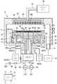
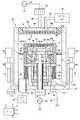
도 1에, 본 발명의 일실시예에서의 플라즈마 처리 장치의 구성을 도시한다. 이 플라즈마 처리 장치는, 하부 2 주파 인가 방식의 용량 결합형 플라즈마 처리 장치로서 구성되어 있고, 예를 들면 알루미늄 또는 스테인리스 스틸 등의 금속제의 원통 형상 챔버(처리 용기)(10)를 가지고 있다. 챔버(10)는 접지되어 있다.Fig. 1 shows the configuration of a plasma processing apparatus in one embodiment of the present invention. This plasma processing apparatus is configured as a capacitively coupled plasma processing apparatus of the lower two-frequency application method, and has a cylindrical chamber (process vessel) 10 made of metal, such as aluminum or stainless steel. The
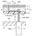
챔버(10) 내에는, 피처리 기판으로서 예를 들면 반도체 웨이퍼(W)를 재치하는 원판 형상의 재치대 또는 서셉터(12)가 수평으로 배치되어 있다. 이 서셉터(12)는, 챔버(10)의 바닥으로부터 수직 상방으로 연장되는 유전체 예를 들면 세라믹제의 통 형상 지지부(14)에 의해 비접지로 지지되어 있다. 챔버(10)의 저벽(이 실시예에서는 베이스)(10a)과 서셉터(12)의 하면과 유전체 통 형상 지지부(14)의 내벽과의 사이에는, 대기 공간에 통하고 있는 스페이스(SP)가 형성되어 있다. 서셉터(12)의 하면은 요철(凹凸)이 없는 수평한 평탄면이며, 챔버(10)의 저벽(10a)의 상면도 후술하는 개구(10b, 114)를 제외하고 요철이 없는 수평한 평탄면으로 되어 있다.In the
유전체 통 형상 지지부(14)의 외주를 따라 챔버(10)의 저벽(10a)으로부터 수직 상방으로 연장되는 도전성의 통 형상 지지부(16)와 챔버(10)의 내벽과의 사이에 환상의 배기로(18)가 형성되고, 이 배기로(18)의 바닥에 배기구(20)가 형성되어 있다. 이 배기구(20)에는 배기관(22)을 개재하여 배기 장치(24)가 접속되어 있다. 배기 장치(24)는 터보 분자 펌프 등의 진공 펌프를 가지고 있고, 챔버(10) 내의 처리 공간을 원하는 진공도까지 감압할 수 있다. 챔버(10)의 측벽에는 반도체 웨이퍼(W)의 반입출구를 개폐하는 게이트 밸브(26)가 장착되어 있다.An annular exhaust passage between the inner wall of the
서셉터(12)는 도체 예를 들면 알루미늄으로 이루어지는 배판(28)과, 도체 예를 들면 알루미늄으로 이루어지는 하부 고주파 전극(30)과, 웨이퍼 흡착용의 정전 척(32)을 아래로부터 이 순서로 적층하여 구성되어 있다. 하부 고주파 전극(30)에는 제 1 및 제 2 고주파 전원(34, 36)이 매칭 유닛(38), 급전봉(40) 및 배판(28)을 개재하여 전기적으로 접속되어 있다.The
제 1 고주파 전원(34)은, 주로 플라즈마의 생성에 기여하는 일정 주파수(통상 27 MHz 이상, 바람직하게는 60 MHz 이상)의 제 1 고주파(HF)를 출력한다. 한편 제 2 고주파 전원(36)은, 주로 서셉터(12) 상의 반도체 웨이퍼(W)에 대한 이온의 인입에 기여하는 일정 주파수(통상 13 MHz 이하)의 제 2 고주파(LF)를 출력한다. 매칭 유닛(38)에는, 제 1 및 제 2 고주파 전원(34, 36)과 플라즈마 부하의 사이에서 임피던스의 정합하기 위한 제 1 및 제 2 정합기(도시하지 않음)가 수용되어 있다.The first high
급전봉(40)은 소정의 외경을 가지는 원통 형상 또는 원기둥 형상의 도체로 이루어지고, 그 상단이 서셉터(12)(배판(28))의 하면의 중심부에 접속되고, 그 하단이 매칭 유닛(38) 내의 상기 제 1 및 제 2 정합기의 고주파 출력 단자에 접속되어 있다. 또한, 챔버(10)의 저벽(10a)과 매칭 유닛(38)의 사이에는 급전봉(40)의 주위를 둘러싸는 원통 형상의 도체 커버(42)가 설치되어 있다. 보다 상세하게는, 챔버(10)의 저벽(10a)에 급전봉(40)의 외경보다 한층 큰 소정의 구경을 가지는 원형의 개구부(10b)가 형성되고, 도체 커버(42)의 상단부가 이 챔버(10)의 개구부(10b)에 접속되고, 또한 도체 커버(42)의 하단부가 상기 정합기의 접지(귀선) 단자에 접속되어 있다.The feeding
서셉터(12)는 반도체 웨이퍼(W)보다 한층 큰 직경 또는 구경을 가지고 있다. 서셉터(12)의 상면은, 웨이퍼(W)와 대략 동일 형상(원형) 또한 대략 동일 사이즈의 중심 영역 즉 웨이퍼 재치부와, 이 웨이퍼 재치부의 외측에 연장되는 환상의 주변부로 구획되어 있다. 웨이퍼 재치부 상에, 처리 대상의 반도체 웨이퍼(W)가 재치된다. 환상 주변부 상에는, 반도체 웨이퍼(W)의 구경보다 큰 내경을 가지는 링 형상의 판재 이른바 포커스 링(44)이 장착된다. 이 포커스 링(44)은 반도체 웨이퍼(W)의 피에칭재에 따라, 예를 들면 Si, SiC, C, SiO2 중 어느 하나의 재질로 구성되어 있다.The
서셉터(12)의 상면에 설치되는 정전 척(32)은, 고주파 전극(30)의 상면에 일체 형성 또는 일체 고착된 유전체층(32a) 내에 DC 전극(32b)을 봉입하고 있다. DC 전극(32b)에는 챔버(10)의 밖에 배치되는 외부 부착의 직류 전원(45)이 스위치(46), 고저항값의 저항(47) 및 DC 고압선(48)을 개재하여 전기적으로 접속되어 있다. 직류 전원(45)으로부터의 고압의 직류 전압을 DC 전극(32b)에 인가하면, 정전력에 의해 반도체 웨이퍼(W)를 정전 척(32) 상에 흡착 보지할 수 있도록 되어 있다. 또한 DC 고압선(48)은 피복선이며, 원통체의 급전봉(40) 내를 통과하여, 서셉터(12)의 배판(28) 및 하부 고주파 전극(30)을 아래로부터 관통하여 정전 척(32)의 DC 전극(32b)에 접속되어 있다.The
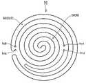
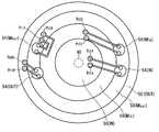
정전 척(32)의 유전체층(32a) 내에는 DC 전극(32b)과 함께 발열체(50)도 봉입되어 있다. 이 발열체(50)는 예를 들면 스파이럴 형상의 저항 발열선으로 이루어지고, 이 실시예에서는 도 2에 도시한 바와 같이, 서셉터(12)의 직경 방향에서 내측의 발열선(50(IN))과 외측의 발열선(50(OUT))으로 2 분할되어 있다.In the
이 중 내측 발열선(50(IN))은, 서셉터(12) 내를 통과하는 내부 도체(51(IN)), 스페이스(SP)를 종단하는 급전 도체(52(IN)), 필터 유닛(54(IN)) 및 전기 케이블(56(IN))을 개재하여, 챔버(10)의 밖에 배치되는 전용의 히터 전원(58(IN))에 전기적으로 접속되어 있다. 외측 발열선(50(OUT))은, 서셉터(12) 내를 통과하는 내부 도체(51(OUT)), 스페이스(SP)를 종단하는 급전 도체(52(OUT)), 필터 유닛(54(OUT)) 및 전기 케이블(56(OUT))을 개재하여, 역시 챔버(10)의 밖에 배치되는 전용의 히터 전원(58(OUT))에 전기적으로 접속되어 있다.Of these, the inner heating wire 50 (IN) includes an inner conductor 51 (IN) passing through the
필터 유닛(54(IN), 54(OUT))의 배치 구성 및 필터 유닛(54(IN), 54(OUT))과 발열체(50)의 사이에서 히터 급전 라인을 배치하는 구성은, 이 실시예에서의 주요한 특징 부분이며, 후에 상세히 설명한다.The arrangement configuration of the filter units 54 (IN) and 54 (OUT) and the arrangement of arranging the heater feeding line between the filter units 54 (IN), 54 (OUT) and the
서셉터(12)에서 하부 고주파 전극(30)의 내부에는 예를 들면 원주 방향으로 연장되는 환상의 냉매 통로(60)가 형성되어 있다. 이 냉매 통로(60)에는 칠러 유닛(도시하지 않음)으로부터 냉매 공급관(62)을 거쳐 소정 온도의 냉매 예를 들면 냉각수(cw)가 순환 공급된다. 냉매의 온도에 의해 서셉터(12)의 온도를 낮추는 방향으로 제어할 수 있다. 그리고, 서셉터(12)에 반도체 웨이퍼(W)를 열적으로 결합시키기 위하여, 전열 가스 공급부(도시하지 않음)로부터의 전열 가스 예를 들면 He 가스가, 가스 공급관(62)을 거쳐 정전 척(32)과 반도체 웨이퍼(W)와의 접촉 계면으로 공급되도록 되어 있다.In the
챔버(10)의 천장에는, 서셉터(12)와 평행하게 마주하여 상부 전극을 겸하는 샤워 헤드(64)가 설치되어 있다. 이 샤워 헤드(64)는, 서셉터(12)와 마주하는 전극판(66)과, 이 전극판(66)을 그 배후(背後)(위)로부터 착탈 가능하게 지지하는 전극 지지체(68)를 가지고, 전극 지지체(68)의 내부에 가스실(70)을 설치하고, 이 가스실(70)로부터 서셉터(12)측으로 관통하는 다수의 가스 토출홀(72)을 전극 지지체(68) 및 전극판(66)에 형성하고 있다. 전극판(66)과 서셉터(12)의 사이의 공간이 플라즈마 생성 공간 내지 처리 공간이 된다. 가스실(70)의 상부에 형성되는 가스 도입구(70a)에는 처리 가스 공급부(74)로부터의 가스 공급관(76)이 접속되어 있다. 전극판(66)은 예를 들면 Si, SiC 혹은 C로 이루어지고, 전극 지지체(68)는 예를 들면 아르마이트 처리된 알루미늄으로 이루어진다.On the ceiling of the
이 플라즈마 처리 장치 내의 각 부 예를 들면 배기 장치(24), 고주파 전원(34, 36), 직류 전원(45)의 스위치(46), 히터 전원(58(IN), 58(OUT)), 칠러 유닛(도시하지 않음), 전열 가스 공급부(도시하지 않음) 및 처리 가스 공급부(74) 등의 개개의 동작 및 장치 전체의 동작(시퀀스)은, 마이크로 컴퓨터를 포함하는 제어부(75)에 의해 제어된다.Each part in this plasma processing apparatus, for example,
이 플라즈마 처리 장치에서 예를 들면 에칭을 행하기 위해서는, 먼저 게이트 밸브(26)를 개방 상태로 하여 가공 대상의 반도체 웨이퍼(W)를 챔버(10) 내로 반입하여, 정전 척(32) 상에 재치한다. 그리고, 처리 가스 공급부(74)로부터 에칭 가스(단일 가스 또는 혼합 가스)를 소정의 유량으로 챔버(10) 내로 도입하고, 배기 장치(24)에 의해 챔버(10) 내의 압력을 설정치로 한다. 또한, 제 1 및 제 2 고주파 전원(34, 36)을 온으로 하여 제 1 고주파(HF) 및 제 2 고주파(LF)를 각각 소정의 파워로 출력시키고, 이들 고주파(HF, LF)를 매칭 유닛(38) 및 급전봉(40)을 개재하여 서셉터(12)의 하부 고주파 전극(30)에 인가한다. 또한, 전열 가스 공급부로부터 정전 척(32)과 반도체 웨이퍼(W)와의 사이의 접촉 계면으로 전열 가스(He 가스)를 공급하고, 또한 정전 척용의 스위치(46)을 온으로 하여, 정전 흡착력에 의해 전열 가스를 상기 접촉 계면에 가둔다. 한편, 히터 전원(58(IN), 58(OUT))을 온으로 하여, 내측 발열선(50(IN)) 및 외측 발열선(50(OUT))를 각각 독립한 줄 열로 발열시켜, 서셉터(12) 상면의 온도 내지 온도 분포를 설정치로 제어한다. 샤워 헤드(64)로부터 토출된 에칭 가스는 서셉터(12)와 샤워 헤드(64)의 사이의 플라즈마 생성 공간에서 고주파의 방전에 의해 플라즈마화하고, 이 플라즈마로 생성되는 라디칼 또는 이온에 의해 반도체 웨이퍼(W) 표면의 피가공막이 원하는 패턴으로 에칭된다.In order to perform, for example, etching in this plasma processing apparatus, the
이 용량 결합형 플라즈마 처리 장치는, 서셉터(12) 내부의 하부 고주파 전극(30)에 플라즈마 생성에 적합한 비교적 높은 주파수(바람직하게는 60 MHz 이상)의 제 1 고주파(HF)를 인가함으로써, 플라즈마를 바람직한 해리 상태에서 고밀도화하여, 보다 저압의 조건하에서도 고밀도 플라즈마를 형성할 수 있다. 이와 동시에, 하부 고주파 전극(30)에 이온 인입에 적합한 비교적 낮은 주파수(13 MHz 이하)의 제 2 고주파(LF)를 인가함으로써, 서셉터(12) 상의 반도체 웨이퍼(W)에 대하여 선택성이 높은 이방성(異方性)의 에칭을 실시할 수 있다.This capacitively coupled plasma processing apparatus applies plasma to the lower
또한 이 용량 결합형 플라즈마 처리 장치에서는, 서셉터(12)에 칠러 유닛의 냉각과 히터의 가열을 동시에 부여하고, 또한 히터의 가열을 반경 방향의 중심부와 엣지부에서 독립적으로 제어하므로, 고속의 온도 전환 또는 온도 상승 및 하강이 가능하고, 또한 온도 분포의 프로파일을 임의 또는 다양하게 제어하는 것도 가능하다.In addition, in this capacitively coupled plasma processing apparatus, since the cooling of the chiller unit and heating of the heater are simultaneously applied to the
(필터 유닛 내의 회로 구성)(Circuit configuration in the filter unit)
이어서, 이 플라즈마 처리 장치에서의 필터 유닛(54(IN), 54(OUT)) 내의 회로 구성을 설명한다.Next, the circuit configuration in the filter units 54 (IN) and 54 (OUT) in this plasma processing apparatus will be described.
도 3에, 서셉터(12)에 내장되는 웨이퍼 온도 제어용의 발열체(50)로 전력을 공급하기 위한 히터 급전부의 회로 구성을 도시한다. 이 실시예에서는, 발열체(50)의 내측 발열선(50(IN)) 및 외측 발열선(50(OUT))의 각각에 대하여 실질적으로 동일한 회로 구성을 가지는 개별의 히터 급전부를 접속하고, 내측 발열선(50(IN)) 및 외측 발열선(50(OUT))의 발열량 또는 발열 온도를 독립적으로 제어하도록 하고 있다. 이하의 설명에서는, 내측 발열선(50(IN))에 대한 히터 급전부의 구성 및 작용에 대하여 기술한다. 외측 발열선(50(OUT))에 대한 히터 급전부의 구성 및 작용도 완전히 동일하다.FIG. 3 shows a circuit configuration of a heater feeding portion for supplying electric power to the
히터 전원(58(IN))은, 예를 들면 SSR(Solid-State Relay)을 이용하여 예를 들면 상용 주파수의 스위칭(ON/OFF) 동작을 행하는 교류 출력형의 전원이며, 내측 발열선(50(IN))과 폐루프의 회로로 접속되어 있다. 보다 상세하게는, 히터 전원(58(IN))의 한 쌍의 출력 단자 중 제 1 출력 단자는 제 1 히터 급전 라인(100(1))을 개재하여 내측 발열선(50(IN))의 제 1 단자(h1A)에 전기적으로 접속되고, 제 2 출력 단자는 제 2 히터 급전 라인(100(2))을 개재하여 내측 발열선(50(IN))의 제 2 단자(h2A)에 전기적으로 접속되어 있다.The heater power source 58 (IN) is, for example, an AC output type power source that performs a switching (ON/OFF) operation at a commercial frequency using, for example, a solid-state relay (SSR), and the inner heating wire 50 ( IN)) and a closed loop circuit. More specifically, the first output terminal of the pair of output terminals of the heater power source 58 (IN) is the first of the inner heating wire 50 (IN) through the first heater feeding line 100 (1). It is electrically connected to the terminal h1A , and the second output terminal is electrically connected to the second terminal h2A of the inner heating wire 50(IN) through the second heater feeding line 100(2). It is done.
필터 유닛(54(IN))은, 제 1 및 제 2 히터 급전 라인(100(1), 100(2))의 도중에 각각 설치되는 제 1 및 제 2 필터(102(1), 102(2))를 가지고 있다. 양 필터(102(1), 102(2))의 회로 구성은 실질적으로 동일하다.The filter unit 54 (IN) is provided with first and second filters 102(1) and 102(2) respectively installed in the middle of the first and second heater feeding lines 100(1) and 100(2). ). The circuit configuration of both filters 102(1) and 102(2) is substantially the same.
보다 상세하게는, 양 필터(102(1), 102(2))는 단일의 코일(104(1), 104(2))을 각각 가지고 있다. 코일(104(1), 104(2))의 상부 단자(제 1 단자) 또는 필터 단자(T(1), T(2))는, 한 쌍의 급전 도체(52(IN1), 52(IN2)) 및 한 쌍의 내부 도체(51(IN1), 51(IN2))를 개재하여 내측 발열선(50(IN))의 양 단자(h1A, h2A)에 각각 접속되어 있다. 코일(104(1), 104(2))의 하부 단자(제 2 단자)는, 콘덴서(106(1), 106(2))를 개재하여 접지 전위의 도전성 부재(예를 들면 챔버(10))에 접속되고, 또한 접속점(n(1), n(2)) 및 전기 케이블(페어 케이블)(56(IN))을 개재하여 히터 전원(58(IN))의 제 1 및 제 2 출력 단자에 각각 접속되어 있다.More specifically, both filters 102(1), 102(2) have a single coil 104(1), 104(2), respectively. The upper terminals (first terminals) or filter terminals T(1) and T(2) of the coils 104(1) and 104(2) are a pair of feed conductors 52 (IN1 ), 52 ( IN2 )) and a pair of inner conductors 51 (IN1 ) and 51 (IN2 ), are connected to both terminals h1A and h2A of the inner heating wire 50 (IN), respectively. The lower terminals (second terminals) of the coils 104(1) and 104(2) are conductive members having a ground potential (for example, the chamber 10) via the capacitors 106(1) and 106(2). ), and also the first and second output terminals of the heater power supply 58 (IN) via a connection point (n(1), n(2)) and an electric cable (pair cable) 56(IN). Connected to each.
이러한 구성의 히터 급전부에서, 히터 전원(58(IN))으로부터 출력되는 전류는, 양극성의 사이클에서는, 제 1 히터 급전 라인(100(1)) 즉 전기 케이블(56(IN)), 코일(104(1)), 급전 도체(52(IN1)) 및 내부 도체(51(IN1))를 통하여 일방의 발열선 단자(h1A)로부터 내측 발열선(50(IN))으로 들어가, 내측 발열선(50(IN))의 각 부에서 통전에 의한 줄 열을 발생시키고, 타방의 발열선 단자(h2A)로부터 나온 후에는, 제 2 히터 급전 라인(100(2)) 즉 내부 도체(51(IN2)), 급전 도체(52(IN2)), 코일(104(2)) 및 전기 케이블(56(IN))을 통화여 귀환한다. 음극성의 사이클에서는, 동일한 회로를 상기와 반대 방향으로 전류가 흐른다. 이 히터 교류 출력의 전류는 상용 주파수이기 때문에, 코일(104(1), 104(2))의 임피던스 또는 그 전압 강하는 무시할 수 있을 정도로 작고, 또한 콘덴서(106(1), 106(2))를 통하여 어스로 빠지는 누설 전류도 무시할 수 있을 정도로 적다.In the heater feeding section of this configuration, the current output from the heater power supply 58 (IN) is, in a bipolar cycle, the first heater feeding line 100 (1), that is, the electric cable 56 (IN), the coil ( 104(1)), enters the inner heating wire 50(IN) from one heating wire terminal h1A through the feeding conductor 52(IN1 ) and the inner conductor 51(IN1 ), and the inner heating wire ( After generating Joule heat by energization in each part of 50(IN), and after exiting from the other heating wire terminal h2A , the second heater feeding line 100(2), that is, the inner conductor 51(IN2 )), the feeding conductor 52 (IN2 ), the coil 104 (2), and the electric cable 56 (IN) are returned by currency. In the negative cycle, current flows in the opposite direction to the same circuit. Since the current of the heater AC output is a commercial frequency, the impedance of the coils 104(1), 104(2) or their voltage drop is negligibly small, and the capacitors 106(1), 106(2) The leakage current through the earth through is also negligibly small.
(필터 유닛의 물리적 구조 및 배치 구성)(Physical structure and arrangement of filter unit)
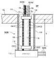
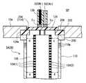
도 4 ~ 도 6에, 이 실시예에서의 필터 유닛(54(IN))의 물리적인 구조 및 배치 구성을 도시한다. 필터 유닛(54(IN))은, 도 4에 도시한 바와 같이 예를 들면 알루미늄으로 이루어지는 원통 형상의 도전성 케이싱(110) 내에 제 1 필터(102(1))의 코일(104(1))과 제 2 필터(102(2))의 코일(104(2))을 동축에 수용하고, 필터 단자(T(1), T(2))의 반대측에서 케이싱(110)의 하단에 결합되어 있는 도전성의 콘덴서 박스(112) 내에 제 1 필터(102(1))측의 콘덴서(106(1))와 제 2 필터(102(2))측의 콘덴서(106(2))(도 3)를 함께 수용하고 있다.4 to 6, the physical structure and arrangement of the filter unit 54 (IN) in this embodiment are shown. The filter unit 54 (IN) is a coil 104 (1) of the first filter 102 (1) in a cylindrical
케이싱(110)은, 급전봉(40)의 주위를 둘러싸는 원통 형상의 도체 커버(42)(도 1)에 인접하여 챔버(10)의 저벽(베이스)(10a)에 형성되어 있는 개구(114)에 챔버(10)의 외측으로부터 수직으로 감합되고, 챔버(10)의 저벽(10a)에 물리적 또한 전기적으로 결합되어 있다. 여기서 케이싱(110)은, 필터 단자(T(1), T(2))의 상면이 챔버(10)의 저벽(10a)의 상면보다 높아지지 않도록(가장 바람직하게는 동일한 높이에서 평면이 되도록), 챔버(10)의 저벽(10a)의 개구(114)에 장착되어 있다. 이 경우, 케이싱(110)의 상단도 챔버(10)의 저벽(10a)의 상면보다 높지 않은 것이 바람직하다.The
각각의 코일(104(1), 104(2))은 공심 코일로 이루어지고, 히터 전원(58(IN))으로부터 내측 발열선(50(IN))에 충분히 큰(예를 들면 30 A 정도의) 전류를 흘리는 급전선의 기능에 더하여, 발열(파워 로스)을 방지하는 관점으로부터 페라이트 등의 자심을 가지지 않고 공심으로 매우 큰 인덕턴스를 얻기 위하여, 또한 큰 선로 길이를 얻기 위하여 굵은 코일선과 큰 코일 사이즈(예를 들면, 직경이 22 ~ 45 mm, 길이 130 ~ 280 mm)를 가지고 있다.Each coil 104(1), 104(2) is made of an air core coil, and is sufficiently large (for example, about 30 A) from the heater power supply 58(IN) to the inner heating wire 50(IN). In addition to the function of the current feeder, the coarse coil wire and the large coil size (eg For example, it has a diameter of 22 to 45 mm and a length of 130 to 280 mm).
원통 형상의 케이싱(110) 내에서, 양 코일(104(1), 104(2))은 절연체 예를 들면 수지로 이루어지는 하부 커넥터(116) 상에 수직으로 세워진 절연체 예를 들면 수지로 이루어지는 원통 또는 원기둥 형상의 봉 축(보빈)(118)의 외주면을 따라 축 방향으로 중첩되어 병진하면서 동일한 권선 간격 및 코일 길이(S)로 나선 형상으로 감겨져 있다. 양 코일(104(1), 104(2))의 각각의 코일 도선은, 도 5에 도시한 바와 같이, 바람직하게는 동일한 단면적을 가지는 박판 또는 평각의 구리선으로 이루어지고, 편방의 공심 코일(104(2))의 코일 도선을 절연체의 튜브(120)로 덮고 있다. 또한, 양 코일(104(1), 104(2))이 접착제 혹은 봉 축(118) 이외의 지지 부재에 의해 일체적으로 안정적으로 보지할 수 있으면, 봉 축(118)을 생략할 수 있다.In the
양 코일(104(1), 104(2))의 하단은, 하부 커넥터(116) 내에서 접속 도체(122(1), 122(2))에 각각 전기적으로 접속되어 있다. 이들 접속 도체(122(1), 122(2))는, 콘덴서 박스(112) 내에서 접속점(n(1), n(2)) 및 콘덴서(106(1), 106(2))(도 3)에 각각 접속되어 있다.The lower ends of both coils 104(1) and 104(2) are electrically connected to the connecting conductors 122(1) and 122(2) in the
케이싱(110)의 상단에 근접하는 위치에서 봉 축(118)의 상단에는, 절연체 예를 들면 수지로 이루어지는 상부 커넥터(124)가 결합되어 있다. 이 상부 커넥터(124)의 상면에는 예를 들면 구리로 이루어지는 판 단편 형상 또는 블록 형상의 필터 단자(T(1), T(2))가 노출된 상태로 돌출되어 설치되어 있다. 이들 필터 단자(T(1), T(2))는, 상부 커넥터(124) 내에서 코일(104(1), 104(2))의 상단에 각각 접속되어 있다.At a position close to the upper end of the
케이싱(110)의 상단은 개구되어 있다. 필터 단자(T(1), T(2))의 상면은 차폐되지 않고, 개방 상태로 서셉터(12) 직하의 스페이스(SP)에 대향하고 있다. 그리고 필터 단자(T(1), T(2))는, 절연체의 지지봉(126)에 봉입되어 있는 핀 형상 또는 봉 형상의 급전 도체(52(IN1), 52(IN2))의 하단에 각각 접속되어 있다.The upper end of the
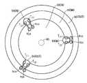
또한 필터 유닛(54(OUT))은, 필터 유닛(54(IN))과 동일한 회로 구성 및 물리적 구조를 가지고, 필터 유닛(54(IN))과는 급전봉(40)의 반대측의 위치 즉 점대칭의 위치에서 챔버(10)의 저벽(베이스)(10a)에 장착된다(도 8).In addition, the filter unit 54 (OUT) has the same circuit configuration and physical structure as the filter unit 54 (IN), and the position opposite to the filter rod 54 (IN) of the
(필터 유닛의 전기적 기능)(Electric function of the filter unit)
이 실시예의 필터 유닛(54(IN))에서는, 제 1 및 제 2 필터(102(1), 102(2))의 코일(104(1), 104(2))과 외도체의 케이싱(110)과의 사이에 분포 정수 선로(105)가 형성된다.In the filter unit 54 (IN) of this embodiment, the coils 104(1), 104(2) of the first and second filters 102(1), 102(2) and the
일반적으로, 전송 선로의 특성 임피던스(Zo)는, 무손실의 경우에는 단위 길이당 정전 용량(C), 인덕턴스(L)를 이용하여 Zo = √(L / C)로 부여된다. 또한 파장(λ)은, 다음의 식 (1)로 부여된다.In general, the characteristic impedance (Zo ) of the transmission line is given by Zo = √ (L / C) using the capacitance (C) per unit length and the inductance (L) in the case of lossless. In addition, wavelength (λ) is given by the following equation (1).
λ = 2π / (ω√(LC))···· (1)λ = 2π / (ω√(LC)) ... (1)
일반적인 분포 정수 선로(특히 동축 선로)에서는 선로의 중심이 봉 형상의 원통 도체인데 반해, 이 필터 유닛(54(IN))에서는 원통 형상의 코일을 중심 도체로 하고 있다는 점이 상이하다. 단위 길이당 인덕턴스(L)는 주로 이 원통 형상 코일에 기인하는 인덕턴스가 지배적으로 된다고 상정된다. 한편, 단위 길이당 정전 용량은, 코일 표면과 외도체가 이루는 콘덴서의 정전 용량(C)으로 규정된다. 따라서, 이 필터 유닛(54(IN))에서도, 단위 길이당 인덕턴스 및 정전 용량을 각각 L, C로 했을 때, 특성 임피던스((Zo) = √(L / C))로 부여되는 분포 정수 선로가 형성되어 있다고 상정할 수 있다.In the general distribution constant line (particularly a coaxial line), the center of the line is a rod-shaped cylindrical conductor, whereas the filter unit 54 (IN) differs in that a cylindrical coil is used as a center conductor. It is assumed that the inductance L per unit length is dominant mainly due to this cylindrical coil. On the other hand, the electrostatic capacity per unit length is defined as the electrostatic capacity (C) of the capacitor formed between the coil surface and the outer conductor. Therefore, even in this filter unit 54(IN), when the inductance and the electrostatic capacity per unit length are L and C, respectively, the distribution constant line given by the characteristic impedance ((Zo ) = √(L / C)) It can be assumed that is formed.
이러한 분포 정수 선로를 가지는 필터 유닛을 단자(T)측에서 보면, 반대측이 큰 용량(예를 들면 5000 pF)을 가지는 콘덴서로 유사적으로 단락되어 있기 때문에, 일정한 주파수 간격으로 큰 임피던스를 반복하는 것과 같은 주파수-임피던스 특성이 얻어진다. 이러한 임피던스 특성은 파장과 분포 선로 길이가 동등할 때 얻어진다.When the filter unit having such a distribution constant line is viewed from the terminal T side, since the opposite side is similarly shorted to a capacitor having a large capacity (for example, 5000 pF), repeating a large impedance at regular frequency intervals The same frequency-impedance characteristics are obtained. This impedance characteristic is obtained when the wavelength and the distribution line length are equal.
이 필터 유닛(54(IN))에서는, 코일(104(1), 104(2))의 권선 길이가 아닌 축 방향의 코일 길이(S)(도 4)가 분포 선로 길이가 된다. 그리고, 중심 도체로 코일(104(1), 104(2))을 이용함으로써, 봉 형상의 원통 도체의 경우에 비해 L을 훨씬 크게 하여 λ를 작게 할 수 있기 때문에, 비교적 짧은 선로 길이(코일 길이(S))이면서 파장과 동등 이상의 실효 길이를 실현하는 것이 가능하며, 비교적 짧은 주파수 간격으로 큰 임피던스를 가지는 것을 반복하는 것과 같은 임피던스 특성을 얻을 수 있다.In this filter unit 54 (IN), the coil length S (FIG. 4) in the axial direction, not the winding length of the coils 104(1) and 104(2), is the distribution line length. In addition, by using the coils 104(1) and 104(2) as the center conductor, it is possible to make λ smaller by making L much larger than that of the rod-shaped cylindrical conductor, so that the relatively short line length (coil length) (S)) It is possible to realize an effective length equal to or greater than the wavelength, and it is possible to obtain an impedance characteristic such as repeating having a large impedance at relatively short frequency intervals.
여기서, 코일(104(1), 104(2))과 케이싱(외도체)(110)의 사이에 형성되는 분포 정수 선로(105) 상에서는 특성 임피던스(특히 단위 길이당의 인덕턴스 및 커패시턴스)가 일정한 것이 바람직하다. 이 점, 도시의 구성예에서는, 원통 형상의 케이싱(외도체)(110) 내에 원통 형상의 코일(104(1), 104(2))이 동축에 배치되므로, 이 특성 임피던스 일정의 요건이 엄밀하게 충족되고 있다. 또한, 코일(104(1), 104(2))과 케이싱(외도체)(110) 간의 갭(거리 간격)에 다소의 요철이 있어도, 허용 범위(일반적으로 차단해야 할 고주파의 파장의 1/4 이하) 내이면, 특성 임피던스 일정의 요건은 실질적으로 충족된다.Here, it is preferable that the characteristic impedance (especially inductance and capacitance per unit length) is constant on the distribution
이와 같이, 각각의 필터(102(1), 102(2))에서는 다중 병렬 공진을 이루고, 또한 임피던스 특성의 안정성·현성이 뛰어난 필터 특성을 얻을 수 있다.As described above, the filter characteristics of the filters 102(1) and 102(2), which achieve multiple parallel resonances, and have excellent stability and realization of impedance characteristics, can be obtained.
(히터 급전 라인의 배치 구성)(Arrangement of heater feeding line)
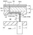
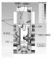
도 7 및 도 8에, 서셉터(12)의 내부 및 직하에서의 히터 급전 라인(100(1), 100(2))의 배치 구성을 도시한다. 도 7에 도시한 바와 같이, 절연체의 지지봉(126) 및 그 중에 봉입되어 있는 급전 도체(52(IN1), 52(IN2))는, 도중에 꺽이지 않고 수직 방향으로 직선으로 연장되어 스페이스(SP)를 종단하고 있다. 그리고, 급전 도체(52(IN1), 52(IN2))의 선단부는, 서셉터(12)(배판(28))의 하면에 전기적으로 절연되어 동일 평면에 장착되어 있는 소켓 단자(128)에 삽입되어 있다.7 and 8, arrangement arrangements of heater feeding lines 100(1) and 100(2) inside and under the
필터 단자(T(1), T(2))와 소켓 단자(128)는, 내측 발열선(50(IN))의 단자(h1A, h2A)보다 챔버(10)의 중심 쪽에 위치하고 있다(도 8). 서셉터(12)의 배판(28) 및 하부 고주파 전극(30)에는 내부 도체(51(IN1), 51(IN2))를 통하기 위한 터널 형상의 통로(132(132a, 132b, 132c))가 형성되어 있다(도 7).The filter terminals T(1) , T(2) and the
보다 상세하게는, 배판(28)의 내부에는, 소켓 단자(128)로부터 발열선 단자(h1A, h2A)의 바로 밑까지 수평으로 연장되는 수평 통로(132a)와, 이 수평 통로(132a)의 종단으로부터 배판(28)의 상면까지 수직 상방으로 연장되는 수직 통로(132b)가 형성되어 있다. 또한 하부 고주파 전극(30)에는, 배판(28)측의 수직 통로(132b)와 중첩되는 위치에서 수직 방향으로 연장되는 관통홀의 수직 통로(132c)가 형성되어 있다. 내부 도체(51(IN1), 51(IN2))는 예를 들면 도전율이 높은 금속 예를 들면 구리로 이루어지고, 예를 들면 수지로 이루어지는 절연체(134)에 의해 배판(28) 및 하부 고주파 전극(30)으로부터 전기적으로 절연된 상태에서 통로(132(132a, 132b, 132c)) 내를 통과하고, 소켓 단자(128)와 정전 척(32) 내의 발열선 단자(h1A, h2A)를 전기적으로 연결한다. 내부 도체(51(IN1), 51(IN2))는 핀 형상, 봉 형상 또는 판 형상 등 어떠한 형태를 채용해도 된다.More specifically, inside the
또한 통로(132) 내에 설치하는 절연체(134)를 최소한으로 해결하기 위하여, 도 9에 도시한 바와 같이, 배판(28)의 수평 통로(132a) 내에서는 내부 도체(51(IN1), 51(IN2)) 아래에만 절연체(134)를 설치하고(깔고), 배판(28)의 수직 통로(132b) 내 및 하부 고주파 전극(30)의 수직 통로(132c) 내에서는 절연체(134)를 전부 생략해도 된다.In addition, in order to minimize the
(실시예에서의 작용)(Operation in Examples)
이 플라즈마 처리 장치는, 필터 유닛(54(IN), 54(OUT))의 배치 및 서셉터(12) 주변의 히터 급전 라인(100(1), 100(2))의 배치에 관하여 상기와 같은 구성을 채용함으로써, 서셉터(12) 상의 플라즈마 밀도 분포 특성 또는 반도체 웨이퍼(W) 상의 프로세스 특성(예를 들면 에칭 레이트 특성)의 면내 균일성을 크게 향상시킬 수 있다.This plasma processing apparatus is as described above with respect to the arrangement of the filter units 54 (IN) and 54 (OUT) and the arrangement of the heater feeding lines 100(1) and 100(2) around the
상기한 바와 같이, 서셉터에 발열체를 내장하고, 그 발열체로 전력을 공급하는 히터 급전 라인 상에서 고주파 노이즈를 저지하거나 또는 감쇠시키기 위한 필터를 구비하는 종래의 플라즈마 처리 장치에서는, 필터 유닛의 배치 위치와 서셉터 주변의 히터 급전 라인의 배치가, 서셉터 상의 플라즈마 밀도 분포 특성 또는 반도체 웨이퍼 상의 프로세스 특성에 대하여 비대칭 구조의 한 요인이 되고 있다. 구체적으로, 고주파 전원으로부터 서셉터의 하부 고주파 전극에 인가된 고주파의 일부가 발열체를 통하여 히터 급전 라인 상에 누설됨으로써, 서셉터 직하의 스페이스 내에서 연장되어 있는 히터 급전 라인의 근방에서 플라즈마 밀도 또는 에칭 레이트가 아래로 끌어당겨지듯이 낮아진다. 즉, 서셉터 직하의 스페이스 내에서 연장되어 있는 히터 급전 라인의 평면시적인 이미지가, 서셉터 상의 플라즈마 밀도 분포를 흐트러뜨리는 특이점으로서 플라즈마 생성 공간에 반영 또는 투영된다.As described above, in a conventional plasma processing apparatus having a filter for preventing or attenuating high-frequency noise on a heater feeding line that embeds a heating element in a susceptor and supplies electric power to the heating element, the arrangement position of the filter unit and The arrangement of the heater feeding line around the susceptor is a factor in the asymmetric structure with respect to the plasma density distribution characteristic on the susceptor or the process characteristic on the semiconductor wafer. Specifically, a part of the high frequency applied to the lower high frequency electrode of the susceptor from the high frequency power source leaks onto the heater feeding line through the heating element, thereby plasma density or etching in the vicinity of the heater feeding line extending in the space directly under the susceptor. The rate is lowered as it is pulled down. That is, a planar image of the heater feeding line extending in the space directly under the susceptor is reflected or projected in the plasma generation space as a singularity that disturbs the plasma density distribution on the susceptor.
본 발명자가 서셉터 주변(특히 그 직하)의 전위 분포 및 전계 분포를 전자계 계산에 의해 해석한 바, 히터 급전 라인 상의 전위는, 서셉터 직하의 스페이스 내에서는 급전봉 또는 하부 고주파 전극의 표면 전위와 동일한 정도로 높고(예를 들면 수천 볼트 정도 있음), 필터 유닛 내로 들어오면 코일의 임피던스에 의해 코일축 방향을 따라 점점 강하하여, 코일의 종단에서 수십 볼트가 되는 것을 알 수 있었다.When the present inventors analyzed the electric potential distribution and electric field distribution around the susceptor (especially directly below it), the electric potential on the heater feeding line is equal to the surface potential of the feeding rod or the lower high-frequency electrode in the space directly under the susceptor. It was found that the same degree was high (for example, several thousand volts), and when it came into the filter unit, it gradually descended along the coil axis direction by the impedance of the coil, resulting in tens of volts at the coil end.
그런데, 종래의 플라즈마 처리 장치에서는, 서셉터와 챔버의 저벽과의 사이의 스페이스 내에 필터 유닛을 배치하고, 또한 그 스페이스 내에서는 히터 급전 라인(급전 도체)을 횡 방향으로 배치하고 있다. 이 경우, 스페이스 내에서 횡 방향으로 연장되어 있는 히터 급전 라인(급전 도체)의 평면시적인 이미지 또는 필터 유닛의 상면(덮개)의 평면시적인 이미지가, 서셉터 상의 플라즈마 밀도 분포에 비대칭 또한 큰 면적으로 투영된다.By the way, in the conventional plasma processing apparatus, the filter unit is arrange|positioned in the space between the susceptor and the bottom wall of a chamber, and the heater feeding line (feeding conductor) is arrange|positioned in the horizontal direction in the space. In this case, a planar image of the heater feeding line (feeding conductor) extending in the transverse direction in the space or a planar image of the top surface (cover) of the filter unit projects an asymmetrical large area onto the plasma density distribution on the susceptor. do.
또한 종래의 플라즈마 처리 장치에서는, 챔버의 직경 방향에서도 필터 유닛(특히 외측 발열체용의 필터 유닛)의 배치 위치를 고려하고 있지 않고, 서셉터 주변부의 직하에 배치하는 경우가 있다. 그 경우에는, 스페이스 내에서 배치되어 있는 고전압의 히터 급전 라인(급전 도체)이 안테나가 되어, 그로부터 주위의 접지 전위 부재에, 예를 들면 고주파를 투과하기 쉬운 유전체의 통 형상 지지부(14)를 개재하여 접지 전위의 도전성 통 형상 지지부(16)에 고주파의 전파를 방사하는 경우가 있으며, 이에 의해 필터의 고주파 차단 기능이 현저하게 저하된다.Moreover, in the conventional plasma processing apparatus, the arrangement position of the filter unit (especially the filter unit for the outer heating element) is not considered even in the radial direction of the chamber, and may be arranged directly under the periphery of the susceptor. In that case, a high-voltage heater feeding line (feeding conductor) arranged in the space serves as an antenna, from which the surrounding ground potential member is interposed with, for example, a
이 점, 본 발명은, 필터 유닛(54(IN), 54(OUT))을 서셉터(12) 직하의 스페이스(SP) 내에 넣지 않는 배치 구성으로 하고 있다. 특히 이 실시예에서는, 필터 유닛(54(IN))의 케이싱(110)의 상단이 서셉터(12)의 직하에서 챔버(10)의 저벽(베이스)(10a)의 상면과 동일한 높이로 하여, 또는 챔버(10)의 저벽(10a)의 상면보다 낮게 하여 챔버(10)의 저벽(10a)의 개구(114)에 장착된다. 이에 의해, 케이싱(110)에 수용되어 있는 코일(104(1), 104(2))은 접지 전위의 챔버(10)의 저벽(10a)의 상면보다 낮은 위치에 배치되므로, 서셉터(12)로부터는 챔버(10)의 저벽(10a)에 의해 전자적으로 차폐되어, 플라즈마 생성 공간에는 투영되지 않는다. 즉, 플라즈마 밀도 분포를 흐트러뜨리는 특이점은 되지 않는다. 필터 유닛(54(OUT))측의 코일(104(1), 104(2))도 동일하다.In this respect, the present invention has a configuration in which the filter units 54 (IN) and 54 (OUT) are not placed in the space SP directly under the
한편, 스페이스(SP) 내에서 배치되는 급전 도체(52(IN1), 52(IN2))는 서셉터(12) 상의 플라즈마 밀도 분포에 투영되지만, 옆으로 꺾이지 않고 수직 방향으로 직선으로 연장되어 있으므로, 그 투영 면적은 가급적 작다. 또한, 챔버(10)의 중심 쪽에 위치하고 있다. 이 때문에, 서셉터(12) 상의 플라즈마 밀도 분포에 주는 영향도는 매우 작다. 필터 유닛(54(OUT))측의 급전 도체(52(OUT1), 52(OUT2))도 동일하다.On the other hand, the feeding conductors 52 (IN1 ) and 52 (IN2 ) disposed in the space SP are projected onto the plasma density distribution on the
또한, 서셉터(12)의 내부에서 배치되어 있는 내부 도체(51(IN1), 51(IN2))는, 도체의 배판(28) 및 하부 고주파 전극(30)의 통로(132) 내에 전부 수용되어 있으므로(감춰져 있으므로), 플라즈마 생성 공간에 영향을 주지 않고, 서셉터(12) 상의 플라즈마 밀도 분포를 흐트러뜨릴 우려는 전혀 없다.In addition, the inner conductors 51 (IN1 ) and 51 (IN2 ) disposed inside the
또한 이 실시예에서는, 급전 도체(52(IN1), 52(IN2))를 챔버(10)의 중심 쪽에 배치하고, 유전체 통 형상 지지부(14)로부터 충분히 격리시키고 있으므로, 급전 도체(52(IN1), 52(IN2))로부터 유전체 통 형상 지지부(14)를 개재하여 접지 전위의 도전성 통 형상 지지부(16)에 고주파의 전파가 방사될 우려는 없다. 필터 유닛(54(OUT))측의 급전 도체(52(OUT1), 52(OUT2))도 동일하다.Also, in this embodiment, since the feeding conductors 52 (IN1 ) and 52 (IN2 ) are disposed at the center of the
또한 필터 유닛(54(IN))에서는, 케이싱(110)의 상단이 개구되고, 필터 단자(T(1), T(2))는 노출되어, 차폐되지 않고, 개방 상태로 서셉터(12) 직하의 스페이스(SP)에 임하고 있다. 그리고 급전 도체(52(IN1), 52(IN2))는 물론, 그들을 봉입하고 있는 절연체의 지지봉(126)도 챔버(10)의 저벽(10a)(개구(114)의 내측면)에는 접촉하고 있지 않다. 이에 의해, 후술하는 바와 같이 필터 단자(T(1), T(2)) 부근의 부유 용량을 충분히 작게 하여, 필터(102(1), 102(2))의 주파수-임피던스 특성을 안정화할 수 있다. 필터 유닛(54(OUT))에서도 동일하다.In addition, in the filter unit 54 (IN), the upper end of the
도 10a 및 도 10b에, 이 실시예에서의 필터 유닛(54(IN), 54(OUT))의 배치 및 급전 도체(52(IN1), 52(IN2), 52(OUT1), 52(OUT2))의 배치에 대하여, 바람직하지 않은 몇 개의 예(X1 ~ X5)를 도시한다.10A and 10B, the arrangement and feeding conductors 52(IN1 ), 52(IN2 ), 52(OUT1 ), 52 of the filter unit 54(IN), 54(OUT) in this embodiment For the arrangement of (OUT2 )), several undesirable examples (X1 to X5 ) are shown.
예를 들면, 스페이스(SP) 내에서 급전 도체(52(OUT1), 52(OUT2))를 횡 방향으로 배치하는 것(도 10a의 X1)은, 상술한 바와 같이 서셉터(12) 상의 플라즈마 밀도 분포에 투영되는 급전 도체(52(OUT1), 52(OUT2))의 평면시적인 이미지가 커지므로, 바람직하지 않다. 또한, 챔버(10)의 저벽(10a)의 개구(114) 부근에서 급전 도체(52(IN1), 52(IN2))를 횡으로 배치하는 것(도 10a의 X2)은, 급전 도체(52(IN1), 52(IN2))가 챔버(10)의 저벽(10a)에 접근하여 부유 용량이 커지므로, 바람직하지 않다. 또한, 필터 유닛(54(OUT))의 케이싱(110)을 챔버(10)의 저벽(10a)의 상면보다 높게 하는 것(도 10a의 X3)도, 그 부분이 서셉터(12) 상의 플라즈마 밀도 분포에 투영되므로, 바람직하지 않다.For example, arranging the feeding conductors 52 (OUT1 ) and 52 (OUT2 ) in the horizontal direction in the space SP (X1 in FIG. 10A ), the
급전 도체(52(OUT1), 52(OUT2))를 유전체 통 형상 지지부(14)에 근접시키는 것(도 10b의 X4)은, 상술한 바와 같이 급전 도체(52(OUT1), 52(OUT2))로부터 유전체 통 형상 지지부(14)를 개재하여 접지 전위의 도전성 통 형상 지지부(16)에 고주파의 전자파가 방사되기 쉬워지므로, 바람직하지 않다. 예를 들면, 비유전율이 10인 세라믹으로 이루어지는 유전체 통 형상 지지부(14)의 고주파에 대한 투과성은, 그 1/10의 두께의 스페이스와 동등하다. 즉, 유전체 통 형상 지지부(14)가 개재되어 있음으로써, 급전 도체(52(OUT1), 52(OUT2))는 접지 전위의 도전성 통 형상 지지부(16)에 더 근접하게 된다.The proximity of the power supply conductors 52 (OUT1 ) and 52 (OUT2 ) to the dielectric cylindrical support 14 (X4 in FIG. 10B) is as described above for the power supply conductors 52 (OUT1 ), 52 (OUT2 )) is not preferable because high-frequency electromagnetic waves are easily radiated to the conductive
또한, 챔버(10)의 저벽(10a)의 개구(114)에 필터 단자(T(1), T(2)) 또는 급전 도체(52(IN1), 52(IN2))의 하단부를 덮는 것과 같은 커버(136)를 설치하는 것(도 10b의 X5)은, 그 재질 여하에 관계없이(도체 또는 유전체 중 어느 것이라도), 그것이 챔버(10)의 저벽(10a) 위로 돌출되면 서셉터(12) 상의 플라즈마 밀도 분포에 투영되므로 바람직하지 않고, 또한 필터 단자(T(1), T(2)) 부근의 부유 용량이 커지므로 바람직하지 않다.In addition, the
도시는 생략하지만, 서셉터(12)의 하면 또는 챔버(10)의 저벽(10a)으로부터 스페이스(SP)로 돌출되는 돌기물이 있는 것도, 서셉터(12) 상의 플라즈마 밀도 분포에 영향을 주므로, 바람직하지 않다.Although not shown, the presence of a protrusion protruding from the
도 11에, 이 실시예에서 고주파 전원(34(36))으로부터 제 1 히터 급전 라인(100(1))을 통하여 고주파의 노이즈가 그라운드로 흐르는 고주파 전반로의 등가 회로를 도시한다. 이 등가 회로에서 콘덴서(140)는, 고주파 전극(30)과 내측 발열선(50(IN)) 내지 내부 도체(51(IN1)) 간의 정전 용량이다. 저항(142)은 주로 내측 발열선(50(IN))의 저항이다. 인덕터(144)는 급전 도체(52(IN1))의 인덕턴스이며, 콘덴서(146)는 급전 도체(52(IN1)) 및 필터 단자(T(1)) 부근의 부유 용량이다. 또한, 필터(102(1)) 내의 부유 용량 및 저항분은 무시(생략)하고 있다.Fig. 11 shows an equivalent circuit of the high-frequency propagation path in which high-frequency noise flows from the high-frequency power supply 34 (36) to the ground through the first heater feeding line 100 (1) in this embodiment. In this equivalent circuit, the
이 등가 회로에서, 서셉터(12)로부터 인덕터(144), 콘덴서(부유 용량)(146), 필터(102(1)) 내의 코일(104(1)) 및 콘덴서(106(1))를 거쳐 접지 전위에 이르기까지의 고주파 전반로를 예상했을 때의 주파수-임피던스 특성(ZA(f))은, 예를 들면 도 12에 나타내는 바와 같은 것이 된다. 또한, 서셉터(12)로부터 인덕터(144) 및 콘덴서(부유 용량)(146)를 거쳐 접지 전위에 이르기까지의 고주파 전반로를 예상했을 때의 주파수-임피던스 특성(ZB(f))은, 예를 들면 도 13에 나타낸 것과 같이 된다.In this equivalent circuit, from
필터(102(1))의 주파수-임피던스 특성(ZA(f))은, 코일(104(1))과 외도체의 케이싱(110)에 의해 형성되는 분포 정수 선로(105)의 주파수-임피던스 특성(다중 병렬 공진 특성)과, 인덕터(144) 및 콘덴서(부유 용량)(146)로 이루어지는 LC 직렬 회로(150)의 주파수-임피던스 특성(ZB(f))이 합성된 것이다. 즉, 분포 정수 선로(105)의 주파수-임피던스 특성은, 그 전단에 위치하는 LC 직렬 회로(150)의 주파수-임피던스 특성에 의해, LC 직렬 회로(150)의 직렬 공진 주파수(fSR)를 향해 주파수가 높아질수록 다중 병렬 공진 특성에서의 병렬 공진점의 피크값은 점차 낮아진다.The frequency-impedance characteristic (ZA(f) ) of the filter 102(1) is the frequency-impedance of the distribution
여기서, LC 직렬 회로(150)의 주파수-임피던스 특성(ZB(f))에서는, 커패시터(146)의 정전 용량이 커질수록, 도 13에 나타낸 바와 같이 직렬 공진 주파수(fSR)가 낮은 값이 되고(fSR → fSR'), 그보다 낮은 주파수 영역에서의 임피던스가 전체적으로 낮아진다(ZB(f) → ZB(f)'). 그러면, 도 12에 나타낸 바와 같이, 필터(102(1))의 주파수-임피던스 특성(ZA(f))에서도, 직렬 공진 주파수(fSR)보다 낮은 모든 병렬 공진점 및 주파수 영역에서 임피던스가 낮아진다(ZA(f) → ZA(f)').Here, in the frequency-impedance characteristic (ZB(f) ) of the
또한, 플라즈마 생성용의 제 1 고주파(HF)의 기본 주파수가 예를 들면 100 MHz의 경우, 그 제 2 고조파의 주파수는 200 MHz이다. 여기서, 예를 들면 도 13에 나타낸 바와 같이, 직렬 공진 주파수(fSR)가 낮은 주파수 영역으로 이동하여 제 2 고조파의 주파수(200 MHz)에 가까워지면, 히터 급전 라인(100(1)) 상에서 제 2 고조파의 대전류가 흐른다.In addition, when the fundamental frequency of the first high frequency (HF) for plasma generation is, for example, 100 MHz, the frequency of the second harmonic is 200 MHz. Here, for example, as shown in FIG. 13, when the series resonant frequency fSR moves to a low frequency region and approaches the frequency of the second harmonic (200 MHz), it is removed on the heater feeding line 100(1). 2 A large current of harmonic flows.
따라서, 필터(102(1))의 고주파 차단 기능을 안정화시키기 위해서는, 급전 도체(52(IN1)) 및 필터 단자(T(1)) 주변의 부유 용량(146)을 가급적 작게 하는 것이 중요해진다. 이 실시예에서는, 상기한 바와 같이, 필터 유닛(54(IN))에서는 케이싱(110)의 상단이 개구되고, 필터 단자(T(1))는 노출되어, 차폐되지 않고 개방 상태로 서셉터(12) 직하의 스페이스(SP)에 대향하고 있다. 그리고, 급전 도체(52(IN1))는 물론, 그것을 봉입하고 있는 절연체의 지지봉(126)도 챔버(10)의 저벽(10a)(개구(114)의 내측면)에는 접촉하고 있지 않다. 이에 의해, 부유 용량(146)을 가급적 작게 하여, LC 직렬 회로(150)의 직렬 공진 주파수(fSR)를 가급적 높은 주파수 영역으로 설정하고, 필터(102(1))의 주파수-임피던스 특성(특히 다중 병렬 공진 특성)을 안정화시키고 있다. 이는, 제 2 히터 급전 라인(100(2))에서도 동일하다.Therefore, in order to stabilize the high-frequency blocking function of the filter 102(1), it is important to make the floating
또한 이 실시예에서, 필터 유닛(54(IN), 54(OUT))의 케이싱(110)을 챔버(10)의 저벽(10a)의 개구(114)로부터 격리시켜 챔버(10)의 저벽(10a) 하측에 배치하는 것은 가능하기는 하지만, 바람직한 것은 아니다. 즉, 챔버(10)의 저벽(10a)의 개구(114)가 관통하여 개방되어 있으면, 그곳이 서셉터(12) 상의 플라즈마 밀도 분포를 위로 끌어당기는 반대 방향의 특이점이 될 뿐 아니라, 급전 도체(52(IN1), 52(IN2))가 그 개구(114)를 통과함으로써 급전 도체(52(IN1), 52(IN2)) 주변의 부유 용량(146)이 커진다. 또한 대기 중의 먼지, 티끌, 수분 등이 개구(114)를 출입한다는 점에서도, 바람직하지 않다. 따라서, 필터 유닛(54(IN), 54(OUT))의 케이싱(110)은 챔버(10)의 저벽(10a)의 개구(114)를 막도록 장착되는 것이 바람직하고, 이 실시예와 같이 필터 단자(T(1), T(2))의 상면이 챔버(10)의 저벽(10a)의 상면과 동일한 높이가 되도록 장착되는 것이 가장 바람직하다.Also in this embodiment, the
(다른 실시예 또는 변형예)(Other examples or modifications)
이상 본 발명의 적합한 실시예에 대하여 설명했지만, 본 발명은 상기 실시예에 한정되지 않고, 그 기술 사상의 범위 내에서 각종 변형이 가능하다.The preferred embodiments of the present invention have been described above, but the present invention is not limited to the above embodiments, and various modifications are possible within the scope of the technical idea.
예를 들면, 상기 실시예의 플라즈마 처리 장치에서는, 도 14 및 도 15에 도시한 바와 같이, 서셉터(12)에 절연체의 배판(152)을 설치하는 구성도 가능하다. 이 배판(152)은, 상면이 하부 고주파 전극(30)의 상면에 접합하고, 하면이 스페이스(SP)에 임하고 있다.For example, in the plasma processing apparatus of the above embodiment, as shown in Figs. 14 and 15, it is also possible to provide the insulator back
배판(152)의 중심부에는, 급전봉(40)을 하부 고주파 전극(30)측으로 통하게 하기 위한 관통홀(153)이 형성되어 있다. 또한 배판(152)의 필터 유닛(54(IN), 54(OUT))의 직상에 위치하는 부위에는, 급전 도체(52(IN1), 52(IN2)) 및 급전 도체(52(OUT1), 52(OUT2))를 하부 고주파 전극(30)측으로 통하게 하기 위한 관통홀(154(IN), 154(OUT))도 형성되어 있다.A through
하부 고주파 전극(30)의 하면에는 급전 도체(52(IN1), 52(IN2))의 상단을 수용하는 소켓 단자(156)가 설치된다. 또한 하부 고주파 전극(30)에는 소켓 단자(156)로부터 발열선 단자(h1A, h2A)의 바로 아래까지 수평으로 연장되는 홈(158)이 하면에 형성되고, 또한 홈(158)의 종단으로부터 하부 고주파 전극(30)의 상면까지 수직 상방으로 연장되는 관통홀의 수직 통로(160)가 형성되어 있다. 내부 도체(51(IN1), 51(IN2))는 소켓 단자(156)로부터 배판(152)의 상면을 뻗어 나가도록 하여 홈(158) 내를 통과하고, 홈(158)의 종단으로부터 수직 통로(160) 내를 올라가 발열선 단자(h1A, h2A)에 도달하고 있다.A
이와 같이, 서셉터(12)에 절연체의 배판(152)을 설치할 경우, 하부 고주파 전극(30)의 하면에 형성된 홈(158) 내에서 내부 도체(51(IN1), 51(IN2))를 횡 방향으로 배치하는 구성을 채용함으로써, 내부 도체(51(IN1), 51(IN2))가 하부 고주파 전극(30) 내에 감춰지고, 또한 하부 고주파 전극(30)의 하면의 평탄성도 실질적으로 확보된다. 이 때문에, 내부 도체(51(IN1), 51(IN2))의 배치에 의해 서셉터(12) 상의 플라즈마 밀도 분포가 영향을 받지 않는다.In this way, when the insulator back
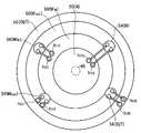
상기한 실시예에서는, 서셉터(12)에 내장되는 발열체(50)가, 서셉터(12)의 직경 방향에서 내측의 발열선(50(IN))과 외측의 발열선(50(OUT))으로 2 분할되어 있었다. 그러나, 발열체(50)를 예를 들면 직경 방향에서, 내측의 발열선(50(IN))과 중간의 발열선(50(MI))과 외측의 발열선(50(OUT))으로 3 분할하는 구성, 혹은 내측의 발열선(50(IN))과 내측 쪽 중간의 발열선(50(MIin))과 외측 쪽 중간의 발열선(50(MIout))과 외측의 발열선(50(OUT))으로 4 분할하는 구성도 가능하다.In the above-described embodiment, the
3 분할식에서는, 도 16a에 도시한 바와 같이, 내측 발열선(50(IN)), 중간 발열선(50(MI)) 및 외측 발열선(50(OUT))에 각각 대응하는 3 개의 필터 유닛(54(IN), 54(MI), 54(OUT))을 챔버(10)의 중심부 즉 급전봉(40) 쪽에서 동심원 상에 등간격(120° 간격)으로 배치하는 것이 바람직하다. 이 경우, 필터 유닛(54(IN))은, 내측 발열선(50(IN))의 단자(h1A, h2A)보다 직경 방향의 내측(중심 쪽)에 배치된다.In the three-part system, as shown in Fig. 16A, three filter units 54 (each corresponding to the inner heating wire 50(IN)), the middle heating wire 50(MI), and the outer heating wire 50(OUT), respectively IN), 54 (MI), 54 (OUT)) are preferably disposed at equal intervals (120° intervals) on concentric circles at the center of the
또한, 이들 필터 유닛(54(IN), 54(MI), 54(OUT))과 유전체 통 형상 지지부(14) 간에 충분한 거리 간격을 취할 수 있을 경우에는, 도 16b에 도시한 바와 같이, 필터 유닛(54(IN))을 내측 발열선(50(IN))의 단자(h1A, h2A)보다 직경 방향의 외측에 배치해도 된다. 단 이 경우에도, 3 개의 필터 유닛(54(IN), 54(MI), 54(OUT))은 동심원 상에 등간격(120° 간격)으로 배치되는 것이 바람직하다.In addition, when a sufficient distance interval between these filter units 54 (IN), 54 (MI), and 54 (OUT) and the dielectric
마찬가지로 4 분할식에서도, 도 17a에 도시한 바와 같이, 내측 발열선(50(IN)), 내측 쪽 중간 발열선(50(MIin)), 외측 쪽 중간 발열선(50(MIout)) 및 외측 발열선(50(OUT))에 각각 대응하는 4 개의 필터 유닛(54(IN), 54(MIin), 54(MIout), 54(OUT))을 챔버(10)의 중심부 즉 급전봉(40) 쪽에서 동심원 상에 등간격(90° 간격)으로 배치하는 것이 바람직하다. 이 경우, 필터 유닛(54(IN))은 내측 발열선(50(IN))의 단자(h1A, h2A)보다 직경 방향의 내측(중심 쪽)에 배치된다.Similarly in the four-segmentation type, as shown in Fig. 17A, the inner heating wire 50(IN), the inner intermediate heating wire 50(MIin ), the outer intermediate heating wire 50(MIout ) and the outer heating wire ( Four filter units 54 (IN), 54 (MIin ), 54 (MIout ), and 54 (OUT), respectively, corresponding to 50 (OUT)) are provided at the center of the
또한, 이들 필터 유닛(54(IN), 54(MIin), 54(MIout), 54(OUT))과 유전체 통 형상 지지부(14) 간에 충분한 거리 간격을 취할 수 있을 경우에는, 도 17b에 도시한 바와 같이 내측 발열선(50(IN)) 혹은 내측 쪽 중간 발열선(50(MIin))보다 직경 방향의 외측에 이들 필터 유닛을 배치하는 것도 가능하다. 그 경우에도, 도 17c에 도시한 바와 같이 4 개의 필터 유닛(54(IN), 54(MIin), 54(MIout), (54(OUT))은 동심원 상에 등간격(90° 간격)으로 배치되는 것이 바람직하다.In addition, when sufficient distance between the filter units 54 (IN), 54 (MIin ), 54 (MIout ), 54 (OUT) and the dielectric
또한 본 발명에서는, 필터 유닛(54)의 내부의 구성에 대해서도 각종 변형이 가능하다. 예를 들면, 필터 유닛(54) 내에 설치되는 필터(102(1), 102(2))는, 상기한 실시예에서는 단일의 공심 코일(104(1), 104(2))을 가지는 것이었지만, 복수의 코일을 직렬 접속하여 이루어지는 구성, 또는 유심 코일(예를 들면 토로이덜 코일)을 가지는 구성 등도 가능하다.Further, in the present invention, various modifications can be made to the internal structure of the
상기 실시예에서는, 서셉터(12)가 챔버(10)의 고정된 저벽(10a) 상에 스페이스(SP)를 개재하여 일정한 높이 위치에 배치되어 있었다. 그러나 도 18에 도시한 바와 같이, 챔버(10) 내에서 서셉터(12)를 상하로 이동 또는 변위 가능하게 구성하고 있는 플라즈마 처리 장치에서는, 서셉터(12)를 유전체 통 형상 지지부(14)를 개재하여 지지하고 있는 승강 가능한 가동 베이스(162)에 필터 유닛(54(IN), 54(OUT))을 장착할 수 있다. 여기서, 서셉터(12)와 유전체 통 형상 지지부(14)와 가동 베이스(162)의 사이에 대기 공간에 통하는 스페이스(SP)가 형성되어 있다.In the above embodiment, the
가동 베이스(162)와 챔버(10)의 저벽(10a)의 사이에는 통 형상의 벨로우즈(164)가 설치되어 있다. 이 벨로우즈(164)는, 배플판(166)을 개재하여 플라즈마 생성 공간(처리 공간)에 연통하는 배기로(18)를 하방으로 연장시키고, 또한 배기로(18) 및 플라즈마 생성 공간(처리 공간)을 대기 공간으로부터 격리 또는 차단하고 있다.A cylindrical bellows 164 is provided between the
벨로우즈(164)에 의해 둘러싸인 공간 내에는, 상부 각부(脚部)(168), 환상 플레이트(170) 및 하부 각부(172)가 종 방향으로 연결되어 설치되어 있다. 상부 각부(168)의 상단은 가동 베이스(162)의 하면에 결합되어 있고, 상부 각부(168)의 하단은 환상 플레이트(170)의 상면에 결합되어 있다. 환상 플레이트(170)의 하면에는 하부 각부(172)의 상단이 결합되어 있다. 하부 각부(172)의 하단은 링크(174)의 플레이트부(174a)에 결합되어 있다.In the space surrounded by the
링크(174)는 상기 플레이트부(174a) 및 2 개의 기둥 형상부(174b)를 포함하고 있다. 플레이트부(174a)는 챔버(10)의 하부의 하방에 설치되어 있다. 이 구성예에서는 플레이트부(174a)에 하부 매칭 유닛(38)이 장착되어 있다.The
플레이트부(174a), 환상 플레이트(170) 및 가동 베이스(162)에는 축선 Z 방향으로 연장되는 관통홀이 각각 형성되어 있고, 하부 급전봉(40)은 이들 관통홀을 통하여 서셉터(12)(도체 배판(28))의 하면까지 수직 방향으로 연장되어 있다.The
기둥 형상부(174b)는 플레이트부(174a)의 주연부로부터 상방으로 연장되어 있다. 또한 기둥 형상부(174b)은, 챔버(10)의 밖에서 챔버(10)의 측벽(10d)과 대략 평행하게 연장되어 있다. 이들 기둥 형상부(174b)에는 예를 들면 볼 나사로 이루어지는 이송 기구가 접속되어 있다. 구체적으로, 2 개의 나사축(176)이 챔버(10)의 측벽(10d)의 외측에서 2 개의 기둥 형상부(174b)와 대략 평행하게 연장되어 있다. 이들 나사축(176)은 2 개의 모터(178)에 각각 접속되어 있다. 또한, 이들 나사축(176)에는 2 개의 너트(180)가 각각 장착되어 있다. 이들 너트(180)에는 2 개의 기둥 형상부(174b)가 각각 결합되어 있다.The
이러한 승강 구동 기구에 의하면, 모터(178)를 회전시킴으로써 너트(180)가 축선 Z 방향으로 이동 즉 상하 이동한다. 너트(180)의 상하 이동에 수반하여, 링크(174)에 가동 베이스(162)를 개재하여 간접적으로 지지되어 있는 서셉터(12)는 축선 Z 방향으로 이동 즉 상하 이동할 수 있다. 또한, 서셉터(12)의 상하 이동에 수반하여 벨로우즈(164)가 신축한다. 그 결과, 서셉터(12)와 상부 전극(64) 간의 거리를 가변으로 조정할 수 있다.According to such a lift drive mechanism, the
또한 이 플라즈마 처리 장치에서, 서셉터(12)에 내장되는 발열체(50)는, 정전 척(32)과 고주파 전극(30)의 사이에 개재한 절연 시트(181) 내에 설치되어 있다. 또한, 상부 전극(64)은 링 형상의 절연체(182)를 개재하여 챔버(10)의 상면에 장착되어 있다. 플라즈마 생성용의 제 1 고주파(HF)를 출력하는 고주파 전원(34)은, 상부 매칭 유닛(184) 및 상부 급전봉(186)을 개재하여 상부 전극(64)에 전기적으로 접속되어 있다. 또한, 이온 인입용의 제 2 고주파(LF)를 출력하는 고주파 전원(36)은, 하부 매칭 유닛(38) 내의 정합기(도시하지 않음) 및 하부 급전봉(40)을 개재하여 서셉터(12)에 전기적으로 접속되어 있다.Moreover, in this plasma processing apparatus, the
본 발명은, 용량 결합형의 플라즈마 에칭 장치에 한정되지 않고, 마이크로파 플라즈마 에칭 장치 또는 유도 결합 플라즈마 에칭 장치, 헬리콘파 플라즈마 에칭 장치 등에도 적용 가능하며, 또한 플라즈마 CVD, 플라즈마 산화, 플라즈마 질화, 스퍼터링 등의 다른 플라즈마 처리 장치에도 적용 가능하다. 또한, 본 발명에서의 피처리 기판은 반도체 웨이퍼에 한정되지 않고, 플랫 패널 디스플레이, 유기 EL, 태양 전지용의 각종 기판 또는 포토마스크, CD 기판, 프린트 기판 등도 가능하다.The present invention is not limited to a capacitively coupled plasma etching apparatus, and can be applied to a microwave plasma etching apparatus, an inductively coupled plasma etching apparatus, a helicon plasma etching apparatus, and the like, and also plasma CVD, plasma oxidation, plasma nitriding, sputtering, etc. It is applicable to other plasma processing apparatuses. In addition, the substrate to be treated in the present invention is not limited to a semiconductor wafer, and various substrates or photomasks, CD substrates, and printed substrates for flat panel displays, organic ELs, and solar cells are also possible.
마이크로파 방전식의 플라즈마 처리 장치, 특히 플라즈마 에칭 장치에서도, 챔버 내에서 피처리 기판 예를 들면 반도체 웨이퍼를 재치하는 재치대 또는 서셉터는, 용량 결합형의 플라즈마 처리 장치와 마찬가지로 기판 보지(척킹) 기능, 바이어스 기능 및 온도 제어 기능을 가진다.Even in a microwave discharge type plasma processing apparatus, particularly a plasma etching apparatus, a mounting table or a susceptor for placing a substrate to be processed, for example, a semiconductor wafer, in a chamber has a substrate holding (chucking) function similarly to a capacitively coupled plasma processing apparatus. , Has bias function and temperature control function.
특히, 온도 제어 기능을 위하여 서셉터에 발열체가 설치될 경우에는, 역시 챔버의 밖에 설치되는 히터 전원으로부터 히터 급전 라인을 거쳐 서셉터 내부의 발열체로 예를 들면 교류 주파수의 전력이 공급된다. 이 경우에도, 서셉터의 고주파 전극에 인가되는 바이어스(이온 인입)용의 고주파의 일부가 발열체를 통하여 히터 급전 라인으로 유입되기 쉽다. 이 때문에, 히터 급전 라인 상에서 고주파의 노이즈를 감쇠시키거나 또는 저지하기 위한 필터가 구비된다. 따라서, 상술한 실시예에서의 필터 유닛(54(IN), 54(OUT)))의 구성 및 서셉터(12)의 내부 및 직하에서의 히터 급전 라인(100(1), 100(2))의 배치 구성을 마이크로파 플라즈마 처리 장치에도 그대로 적용할 수 있다.In particular, when a heating element is installed in the susceptor for temperature control function, power of, for example, an AC frequency is supplied from a heater power source installed outside the chamber to a heating element inside the susceptor through a heater feeding line. Also in this case, a part of the high frequency for bias (ion entrainment) applied to the high frequency electrode of the susceptor is likely to flow into the heater feeding line through the heating element. For this reason, a filter is provided to attenuate or block high frequency noise on the heater feeding line. Therefore, the configuration of the filter units 54 (IN, 54 (OUT)) in the above-described embodiment and the heater feeding lines 100(1), 100(2) inside and under the
단, 마이크로파 플라즈마 처리 장치에서는, 천장 위의 안테나로부터 유전체창을 개재하여 챔버 내에 방사되는 플라즈마 생성용의 통상 2.45 GHz의 마이크로파의 일부가, 플라즈마 및 서셉터를 통과하여 필터 유닛(54(IN), 54(OUT)))으로 유입된다. 여기서, 필터 유닛(54(IN), 54(OUT)))으로 유입된 마이크로파가 밖으로 누설되면, 전파 잡음의 원인이 되는 경우가 있다.However, in the microwave plasma processing apparatus, a part of the normal 2.45 GHz microwave for generating plasma radiated into the chamber via a dielectric window from the antenna on the ceiling passes through the plasma and the susceptor, and the filter unit 54 (IN), 54 (OUT))). Here, when the microwaves flowing into the filter units 54 (IN) and 54 (OUT) leak out, it may cause radio noise.
도 19a ~ 도 19d에, 본 발명에 따라 마이크로파 플라즈마 처리 장치에서 챔버(10)의 저벽(10a)에 필터 유닛(54(IN))을 장착할 경우에 마이크로파 누설 장애를 확실히 방지할 수 있는 구성예를 도시한다. 필터 유닛(54(OUT))도 동일한 구성이다.19A to 19D, a configuration example capable of reliably preventing a microwave leakage failure when the filter unit 54 (IN) is attached to the
도 19a에 도시한 필터 유닛 장착 구조는, 필터 유닛(54(IN))의 케이싱(110)의 상부에 도체 예를 들면 알루미늄으로 이루어지는 와셔 형상의 플랜지(200)를 일체로 형성 또는 결합하고, 이 플랜지(200)의 상면을 베이스 또는 챔버(10)의 저벽(10a)의 하면에 밀착시키고 있다. 챔버(10)의 저벽(10a)에는 상부 커넥터(124)를 수용하는 스폿 페이싱 홀(202)과, 핀 형상의 급전 도체(52(IN1), 52(IN2))를 밀봉하고 있는 절연체 봉(126)을 통하는 개구(204)가 형성되어 있다. 또한 케이싱(110)의 측면에는, 바람직하게는 3 mm 이하의 직경을 가지는 공냉용의 통기홀(110a)이 펀칭 가공에 의해 형성되어 있다.The filter unit mounting structure shown in FIG. 19A integrally forms or joins a washer-shaped
이 장착 구조에서는, 챔버(10)의 저벽(10a)과 필터 유닛(54(IN))의 사이에 마이크로파가 누설되는 간극이 대부분 존재하지 않으므로, 마이크로파 누설 장애를 확실히 방지할 수 있다. 또한, 케이싱(110)의 통기홀(110a)의 직경은 3 mm 이하이므로, 통기홀(110a)로부터 마이크로파가 누설되지 않는다.In this mounting structure, most of the gap between the
도 19b의 필터 유닛 장착 구조는, 챔버(10)의 저벽(10a)에 형성되는 스폿 페이싱 홀(202)에 플랜지(200)를 아래로부터 감합한다. 이 경우, 플랜지(200)는 그 상면뿐 아니라 측면에서도 챔버(10)의 저벽(10a)과 밀착한다. 이 장착 구조에서도, 챔버(10)의 저벽(10a)과 필터 유닛(54(IN))의 사이에 마이크로파가 누설되는 간극이 대부분 존재하지 않으므로, 마이크로파 누설 장애를 확실히 방지할 수 있다. 또한 이 장착 구조에서는, 케이싱(110)에 일체 형성 또는 결합되어 있는 플랜지(200)가 챔버(10)의 저벽(10a)의 스폿 페이싱 홀(202)에 감합됨으로써, 필터 단자(T(1), T(2))의 위치가 규정되고, 나아가서는 급전 도체(52(IN1), 52(IN2))가 서셉터(12)측의 소켓 단자(128(156))(도 7, 도 15)에 대하여 위치 결정되도록 되어 있다.The filter unit mounting structure of FIG. 19B fits the
도 19c ~ 19e에는, 상기한 바와 같이 마이크로파 누설 장애를 방지하는 필터 유닛 장착 구조에서, 케이싱(110) 내에서 분포 정수 선로(105)의 특성 임피던스를 일정하게 유지하는 구성예를 도시한다.19C to 19E show a configuration example in which the characteristic impedance of the distribution
상기한 바와 같이 플랜지(200)의 상면을 베이스 또는 챔버(10)의 저벽(10a)의 하면에 밀착시킬 경우(도 19a), 코일(104(1), 104(2))의 상단부가 플랜지(200) 상에 돌출되어 있으면, 이 돌출된 코일 부분에 반경 방향으로 대향하는 외도체는 케이싱(110)이 아닌, 그보다 큰 구경을 가지는 챔버(10)의 저벽(10a)의 스폿 페이싱 홀(202)의 내벽이며, 이에 따라 분포 정수 선로(동축 선로)(105)의 특성 임피던스가 흐트러지는 경우가 있다.As described above, when the upper surface of the
따라서 도 19c의 구성예는, 상부 커넥터(124)와 플랜지(200)와 챔버(10)의 저벽(10a)의 스폿 페이싱 홀(202)과의 사이에, 중심부가 개구되어 있는 도체 예를 들면 알루미늄으로 이루어지는 캡 형상의 스페이서(206)를 삽입하고, 이 스페이서(206)의 내주면 및 플랜지(200)의 내주면을 케이싱(110)의 내주면과 동일 평면으로 나란히 하여, 코일(104(1), 104(2))과 외도체와의 거리 간격(d)을 분포 정수 선로(동축 선로)(105)의 단부에서 단부까지 일정하게 유지하도록 하고 있다. 또한 도체 스페이서(206)는, 서셉터(12)측의 소켓 단자(128(158))(도 7, 도 15)에 대하여 필터 단자(T(1), T(2)) 및 급전 도체(52(IN1), 52(IN2))의 위치 조정을 또한 용이하고 정확하게 행하기 위한 심으로서 기능한다.Therefore, in the configuration example of FIG. 19C, a conductor having a central opening, for example, aluminum, between the
도 19d의 구성예는, 도체 스페이서(206)를 구비하는 대신에, 챔버(10)의 저벽(10a)의 개구(114)를 케이싱(110)의 내경과 동일한 구경으로 형성하고, 개구(114)의 내벽 및 플랜지(200)의 내주면을 케이싱(110)의 내주면과 동일 평면으로 나란히 하여, 코일(104(1), 104(2))과 외도체와의 거리 간격(d)을 일정하게 유지하도록 하고 있다. 또한, 필터 단자(T(1), T(2)) 및 급전 도체(52(IN1), 52(IN2))의 위치 조정을 위하여, 챔버(10)의 저벽(10a)의 개구(114)에 감합되는 절연체로 이루어지는 링 형상 또는 원통 형상의 플랜지부(208)를 상부 커넥터(124)의 하면에 일체로 형성 또는 결합하고 있다.19D, instead of having the
도 19e의 구성예는, 챔버(10)의 저벽(10a)의 개구(114) 또는 스폿 페이싱 홀(202)에 케이싱(110)측의 플랜지(200)를 감합할 경우, 플랜지(200)의 내주면이 케이싱(110)의 내주면과 동일 평면으로 나란히 하여 코일(104(1), 104(2))의 상단부와 대향하도록 하고 있다.In the configuration example of FIG. 19E, when fitting the
본 발명자는, 필터 유닛(54(IN))에 간극이 있을 경우의 마이크로파 누설 현상을 전자계 계산의 시뮬레이션으로 검증했다. 이 시뮬레이션에서는, 챔버(10)의 저벽(10a)의 개구(114) 대신에 알루미늄으로 이루어지는 원통 형상의 커버체(210)를 케이싱(110)의 상단에 접속했다. 여기서, 커버체(210)의 하단과 케이싱(110)의 상단과의 사이에서, 도 20a에 나타낸 바와 같이 간극를 전혀 만들지 않는 구성을 일실시예로 하고, 도 20b에 나타낸 바와 같이 간극(G)을 만드는 구성을 비교예로 했다. 이 간극(G)의 사이즈는 종(높이)이 8 mm, 횡(폭)이 60 mm였다.The present inventor verified the microwave leakage phenomenon when there is a gap in the filter unit 54 (IN) by simulation of electromagnetic field calculation. In this simulation, a
필터 유닛(54(IN)) 내에 상방으로부터 2.45 GHz의 마이크로파를 도입했을 때의 케이싱(110)의 내부 및 주위의 전계 분포를 전자계 계산에 의해 구한 바, 실시예(도 20a)에서는, 도 21a에 나타낸 바와 같이 마이크로파의 누설은 전혀 없었다. 또한, 케이싱(110)의 통기홀(펀칭 메탈)(110a)에서의 누설도 없었다. 한편 비교예(도 20b)에서는, 도 21b에 나타낸 바와 같이 상기 간극(G)으로부터 마이크로파가 다량으로 누설되는 것을 명확히 확인할 수 있었다.When the microwave of 2.45 GHz was introduced into the filter unit 54 (IN) from above, the electric field distribution inside and around the
또한 본 발명자는, 상기 실시예(도 20a) 및 비교예(도 20b)의 필터 유닛 장착 구조에서, 100 MHz의 고주파에 대해서도 전자계의 누설이 있는지 여부를 상기와 같은 전자계 계산에 의해 구했다. 그 결과, 도시는 생략하지만 상기 실시예(도 20a)에서는 물론, 비교예(도 20b)에서도 전자계의 누설은 전혀 없었다.In addition, in the filter unit mounting structure of the above-mentioned Examples (Fig. 20A) and Comparative Example (Fig. 20B), the inventors determined whether or not there was leakage of an electromagnetic field even at a high frequency of 100 MHz by the above electromagnetic field calculation. As a result, although not shown, there was no leakage of the electromagnetic field in the above-described embodiment (Fig. 20A) and in the comparative example (Fig. 20B).
일반적으로, 전자파(진행파)가 도체의 개구 부분에 도달했을 때, 전자파의 반파장이 개구 부분의 최대 개구 폭보다 작으면, 전자파는 그 개구 부분을 통과할 수 없다고 하는 것이 통설이다. 상기 비교예(도 20b)의 경우, 마이크로파(2.45 GHz)의 반파장은 61 mm인데 반해, 필터 유닛(54(IN))의 상단부에 형성되어 있는 간극(G)의 사이즈는 8 mm × 60 mm이기 때문에, 상기한 통설에 의하면 2.45 GHz의 마이크로파는 간극(G)을 간신히 통과할 수 있게 되며, 상기 시뮬레이션의 결과도 대략 그것과 부합한다.In general, it is common practice that when an electromagnetic wave (progressive wave) reaches the opening portion of a conductor, if the half-wave length of the electromagnetic wave is smaller than the maximum opening width of the opening portion, the electromagnetic wave cannot pass through the opening portion. In the case of the comparative example (FIG. 20B), the half-wave length of the microwave (2.45 GHz) is 61 mm, while the size of the gap G formed at the upper end of the filter unit 54 (IN) is 8 mm × 60 mm. Therefore, according to the above-mentioned general rule, the microwave of 2.45 GHz can barely pass through the gap G, and the result of the simulation roughly corresponds to it.
따라서, 필터 유닛(54(IN)) 측 및 챔버(10)측 중 적어도 하나의 설계 사정으로부터, 필터 유닛(54(IN))과 챔버(10)의 사이에 부득이하게 간극이 형성될 경우에는, 상기 통설에 따르면, 그 간극의 최대 개구 폭을 마이크로파의 반파장의 약 반 이하(약 30 mm 이하)로 억제하면, 마이크로파의 누설을 방지할 수 있다고 하는 것이 된다.Accordingly, in the event of a design situation of at least one of the filter unit 54 (IN) side and the
본 발명자는, 이 점을 확인하기 위한 시뮬레이션도 행했다. 즉, 상기 비교예(도 20b)에 준한 간극이 있는 장착 구조로서, 커버체(210)와 케이싱(110)의 사이에 원형 홀(개구)(G)을 형성하고, 이 원형 홀(G)의 구경을 13 mm, 17 mm, 23 mm, 27 mm, 35 mm의 5 단계로 선택하여, 각 경우에 대하여 필터 유닛(54(IN)) 내에 상방으로부터 2.45 GHz의 마이크로파를 도입했을 때의 케이싱(110)의 내부 및 주위의 전계 분포를 전자계 계산에 의해 구했다. 도 22a ~ 도 22e에 그 시뮬레이션 결과를 나타낸다.The inventor has also performed simulation to confirm this point. That is, as a mounting structure having a gap according to the comparative example (FIG. 20B), a circular hole (opening) G is formed between the
도 22a에 나타낸 바와 같이, 원형 홀(G)의 구경이 13 mm에서도 수 V/m 정도의 누설이 있었다. 그리고, 원형 홀(G)의 구경이 17 mm, 23 mm, 27 mm로 커짐에 따라 전계(마이크로파)의 누설량은 증가하고(도 22b, 도 22c, 도 22d), 35 mm구경에서는 100 V/m 이상의 누설을 발생하는 것을 알 수 있었다(도 22e).As shown in Fig. 22A, even when the diameter of the circular hole G was 13 mm, there was a leakage of about V/m. And, as the diameter of the circular hole G increases to 17 mm, 23 mm, and 27 mm, the leakage amount of the electric field (microwave) increases (Fig. 22b, Fig. 22c, Fig. 22d), and 100 V/m at a diameter of 35 mm. It was found that the above leakage occurred (Fig. 22E).
상기한 시뮬레이션으로부터, 본 발명을 적용하는 마이크로파 플라즈마 처리 장치에서 필터 유닛(54(IN)) 장착 구조 주변에서의 마이크로파 누설 방지를 확실히 보증하기 위해서는, 필터 유닛(54(IN))과 챔버(10)의 사이에 형성되는 간극은, 그 최대 개구 폭이 마이크로파의 반파장 정도(약 60 mm)는 물론, 반파장의 반 정도(약 30 mm)라도 아직 불충분하며, 반파장의 수십분의 1 이하(약 3 mm 이하)로 할 필요가 있는 것을 알 수 있었다.From the above simulation, the filter unit 54(IN) and the
10 : 챔버
12 : 서셉터(하부 전극)
14 : 유전체 통 형상 지지부
28 : (도체) 배판
32 : 정전 척
34, 36 : 고주파 전원
40 : 급전봉
50 : 발열체
50(IN) : 내측 발열선
50(OUT) : 외측 발열선
51(IN1), 51(IN2), 51(OUT1), 51(OUT2) : 내부 도체
52(IN1), 52(IN2), 52(OUT1), 52(OUT2) : 급전 도체
54(IN), 54(OUT), 54(MI), 54(MIin), 54(MIout) : 필터 유닛
100(1), 100(2) : 히터 급전 라인
102(1), 102(2) : 필터
104(1), 104(2) : 코일
T(1), T(2) : 코일의 제 1 단자(필터 단자)
152 : (절연체) 배판10: chamber
12: susceptor (lower electrode)
14: dielectric cylindrical support
28: (conductor) distribution
32: electrostatic chuck
34, 36: high frequency power
40: feeding rod
50: heating element
50(IN): Inside heating wire
50(OUT): Outside heating wire
51(IN1 ), 51(IN2 ), 51(OUT1 ), 51(OUT2 ): Internal conductor
52(IN1 ), 52(IN2 ), 52(OUT1 ), 52(OUT2 ): Feeding conductor
54(IN), 54(OUT), 54(MI), 54(MIin ), 54(MIout ): Filter unit
100(1), 100(2): Heater feeding line
102(1), 102(2): Filter
104(1), 104(2): Coil
T(1) , T(2) : the first terminal of the coil (filter terminal)
152: (insulator) distribution
Claims (20)
Translated fromKorean상기 처리 용기 내에서 판 형상의 도전성 베이스 상에 스페이스를 개재하여 배치되고, 피처리 기판을 재치하여 보지하는 재치대와,
상기 재치대에 설치되는 고주파 전극과,
상기 고주파 전극에 일정 주파수의 고주파를 인가하기 위한 고주파 급전부와,
상기 재치대에 설치되는 발열체와,
상기 발열체를 상기 처리 용기의 밖에 배치되는 히터 전원에 전기적으로 접속하기 위한 히터 급전 라인과,
상기 발열체를 통하여 상기 히터 급전 라인으로 들어오는 고주파의 노이즈를 감쇠시키거나 또는 저지하기 위한 코일과, 상기 코일을 수용하는 케이싱을 가지는 필터 유닛을 가지고,
상기 필터 유닛은, 상기 케이싱의 상단을 상기 재치대의 직하에서 상기 베이스의 상면과 동일한 높이로 하여, 또는 상기 베이스의 상면보다 낮게 하여 배치되고,
상기 베이스에, 상기 히터 급전 라인을 비접촉으로 통하는 개구가 형성되고,
상기 히터 급전 라인이, 상기 베이스의 상기 개구의 내측 또는 하방에 위치하는 상기 코일의 제 1 단자로부터 상기 재치대의 하면까지 상기 스페이스를 통하여 연장되는 핀 형상 또는 봉 형상의 제 1 도체를 가지며,
상기 코일의 제 1 단자의 상면은 상기 베이스의 상면과 동일한 높이인 플라즈마 처리 장치.A processing vessel in which plasma treatment is performed,
A mounting table which is disposed on the plate-shaped conductive base in the processing container via a space, and which mounts and holds the substrate to be processed;
A high-frequency electrode installed on the mounting table,
A high frequency power supply unit for applying a high frequency of a certain frequency to the high frequency electrode,
A heating element installed in the mounting table,
A heater feeding line for electrically connecting the heating element to a heater power source disposed outside the processing container;
A filter unit having a coil for attenuating or blocking high-frequency noise coming into the heater feeding line through the heating element and a casing that accommodates the coil,
The filter unit is disposed with the upper end of the casing at the same height as the upper surface of the base under the mounting table or lower than the upper surface of the base,
In the base, an opening through the heater feed line non-contact is formed,
The heater feeding line has a pin-shaped or rod-shaped first conductor extending through the space from the first terminal of the coil located at the inside or the bottom of the opening of the base to the lower surface of the mounting table,
The upper surface of the first terminal of the coil is a plasma processing apparatus having the same height as the upper surface of the base.
상기 제 1 도체는, 상기 스페이스 내 또는 상기 개구 내에서 꺾이지 않고 직선으로 연장되어 있는 플라즈마 처리 장치.According to claim 1,
The first conductor is a plasma processing apparatus extending in a straight line without bending in the space or in the opening.
상기 제 1 도체는, 상기 스페이스 내 또는 상기 개구 내에서 수직 방향으로 직선으로 연장되어 있는 플라즈마 처리 장치.According to claim 2,
The first conductor is a plasma processing apparatus extending in a straight line in the vertical direction in the space or in the opening.
상기 제 1 도체는 절연체의 봉 내에 봉입되고, 상기 절연체의 봉은 상기 베이스의 상기 개구의 내측면에 접촉하지 않는 플라즈마 처리 장치.The method according to any one of claims 1 to 3,
The first conductor is enclosed in an insulator rod, and the rod of the insulator does not contact the inner surface of the opening of the base.
상기 코일의 제 1 단자는 노출되어 있는 플라즈마 처리 장치.The method according to any one of claims 1 to 3,
A plasma processing apparatus in which the first terminal of the coil is exposed.
상기 코일의 제 1 단자의 상면은, 차폐되지 않고 개방 상태로 상기 스페이스에 대향하고 있는 플라즈마 처리 장치.The method according to any one of claims 1 to 3,
The upper surface of the first terminal of the coil is not shielded, and the plasma processing apparatus faces the space in an open state.
상기 히터 급전 라인이, 상기 제 1 도체의 상단부를 삽입하기 위하여 상기 재치대의 하면에 설치되는 소켓 단자와, 상기 소켓 단자와 상기 발열체의 단자를 전기적으로 연결하기 위하여 상기 재치대 내에서 연장되는 핀 형상, 봉 형상 또는 판 형상의 제 2 도체를 가지는 플라즈마 처리 장치.The method according to any one of claims 1 to 3,
The heater feeding line is a pin shape extending in the mounting table to electrically connect the socket terminal installed on the lower surface of the mounting table to insert the upper end of the first conductor, and the socket terminal and the terminal of the heating element. , Plasma processing apparatus having a rod-shaped or plate-shaped second conductor.
상기 코일의 제 1 단자 및 상기 소켓 단자는, 상기 발열체의 단자보다 상기 처리 용기의 중심 쪽에 위치하는 플라즈마 처리 장치.The method of claim 8,
The first terminal and the socket terminal of the coil are located at the center of the processing container than the terminal of the heating element.
상기 처리 용기 내에서 판 형상의 도전성 베이스 상에 스페이스를 개재하여 배치되고, 피처리 기판을 재치하여 보지하는 재치대와,
상기 재치대에 설치되는 고주파 전극과,
상기 고주파 전극에 일정 주파수의 고주파를 인가하기 위한 고주파 급전부와,
상기 재치대에 설치되는 발열체와,
상기 발열체를 상기 처리 용기의 밖에 배치되는 히터 전원에 전기적으로 접속하기 위한 히터 급전 라인과,
상기 발열체를 통하여 상기 히터 급전 라인으로 들어오는 고주파의 노이즈를 감쇠시키거나 또는 저지하기 위한 코일과, 상기 코일을 수용하는 케이싱을 가지는 필터 유닛을 가지고,
상기 필터 유닛은, 상기 케이싱의 상단을 상기 재치대의 직하에서 상기 베이스의 상면과 동일한 높이로 하여, 또는 상기 베이스의 상면보다 낮게 하여 배치되고,
상기 베이스에, 상기 히터 급전 라인을 비접촉으로 통하는 개구가 형성되고,
상기 히터 급전 라인이, 상기 베이스의 상기 개구의 내측 또는 하방에 위치하는 상기 코일의 제 1 단자로부터 상기 재치대의 하면까지 상기 스페이스를 통하여 연장되는 핀 형상 또는 봉 형상의 제 1 도체를 가지고,
상기 히터 급전 라인이, 상기 제 1 도체의 상단부를 삽입하기 위하여 상기 재치대의 하면에 설치되는 소켓 단자와, 상기 소켓 단자와 상기 발열체의 단자를 전기적으로 연결하기 위하여 상기 재치대 내에서 연장되는 핀 형상, 봉 형상 또는 판 형상의 제 2 도체를 가지고,
상기 재치대는 상면이 상기 고주파 전극의 하면에 접합되고, 하면이 상기 스페이스에 면하는 도체의 배판을 가지고,
상기 제 2 도체는, 상기 배판에 매립된 절연체 내에서 수평 방향으로 연장되는 구간을 가지는 플라즈마 처리 장치.A processing vessel in which plasma treatment is performed,
A mounting table which is disposed on the plate-shaped conductive base in the processing container via a space, and which mounts and holds the substrate to be processed;
A high-frequency electrode installed on the mounting table,
A high frequency power supply unit for applying a high frequency of a certain frequency to the high frequency electrode,
A heating element installed in the mounting table,
A heater feeding line for electrically connecting the heating element to a heater power source disposed outside the processing container;
A filter unit having a coil for attenuating or blocking high-frequency noise coming into the heater feeding line through the heating element and a casing that accommodates the coil,
The filter unit is disposed with the upper end of the casing at the same height as the upper surface of the base under the mounting table or lower than the upper surface of the base,
In the base, an opening through the heater feed line non-contact is formed,
The heater feeding line has a pin-shaped or rod-shaped first conductor extending through the space from the first terminal of the coil located at the inside or the bottom of the opening of the base to the lower surface of the mounting table,
The heater feeding line is a pin shape extending in the mounting table to electrically connect the socket terminal installed on the lower surface of the mounting table to insert the upper end of the first conductor, and the socket terminal and the terminal of the heating element. Has a rod-shaped or plate-shaped second conductor,
The mounting table has a back plate of a conductor whose upper surface is joined to the lower surface of the high-frequency electrode, and the lower surface faces the space,
The second conductor, the plasma processing apparatus having a section extending in the horizontal direction in the insulator embedded in the back plate.
상기 처리 용기 내에서 판 형상의 도전성 베이스 상에 스페이스를 개재하여 배치되고, 피처리 기판을 재치하여 보지하는 재치대와,
상기 재치대에 설치되는 고주파 전극과,
상기 고주파 전극에 일정 주파수의 고주파를 인가하기 위한 고주파 급전부와,
상기 재치대에 설치되는 발열체와,
상기 발열체를 상기 처리 용기의 밖에 배치되는 히터 전원에 전기적으로 접속하기 위한 히터 급전 라인과,
상기 발열체를 통하여 상기 히터 급전 라인으로 들어오는 고주파의 노이즈를 감쇠시키거나 또는 저지하기 위한 코일과, 상기 코일을 수용하는 케이싱을 가지는 필터 유닛을 가지고,
상기 필터 유닛은, 상기 케이싱의 상단을 상기 재치대의 직하에서 상기 베이스의 상면과 동일한 높이로 하여, 또는 상기 베이스의 상면보다 낮게 하여 배치되고,
상기 베이스에, 상기 히터 급전 라인을 비접촉으로 통하는 개구가 형성되고,
상기 히터 급전 라인이, 상기 베이스의 상기 개구의 내측 또는 하방에 위치하는 상기 코일의 제 1 단자로부터 상기 재치대의 하면까지 상기 스페이스를 통하여 연장되는 핀 형상 또는 봉 형상의 제 1 도체를 가지고,
상기 히터 급전 라인이, 상기 제 1 도체의 상단부를 삽입하기 위하여 상기 재치대의 하면에 설치되는 소켓 단자와, 상기 소켓 단자와 상기 발열체의 단자를 전기적으로 연결하기 위하여 상기 재치대 내에서 연장되는 핀 형상, 봉 형상 또는 판 형상의 제 2 도체를 가지고,
상기 재치대는 상면이 상기 고주파 전극의 하면에 접합되고, 하면이 상기 스페이스에 면하는 절연체의 배판을 가지고,
상기 제 2 도체는, 상기 고주파 전극의 하면에 형성된 홈 내에서 수평 방향으로 연장되는 구간을 가지는 플라즈마 처리 장치.A processing vessel in which plasma treatment is performed,
A mounting table which is disposed on the plate-shaped conductive base in the processing container via a space, and which mounts and holds the substrate to be processed;
A high-frequency electrode installed on the mounting table,
A high frequency power supply unit for applying a high frequency of a certain frequency to the high frequency electrode,
A heating element installed in the mounting table,
A heater feeding line for electrically connecting the heating element to a heater power source disposed outside the processing container;
A filter unit having a coil for attenuating or blocking high-frequency noise coming into the heater feeding line through the heating element and a casing that accommodates the coil,
The filter unit is disposed with the upper end of the casing at the same height as the upper surface of the base under the mounting table or lower than the upper surface of the base,
In the base, an opening through the heater feed line non-contact is formed,
The heater feeding line has a pin-shaped or rod-shaped first conductor extending through the space from the first terminal of the coil located at the inside or the bottom of the opening of the base to the lower surface of the mounting table,
The heater feeding line is a pin shape extending in the mounting table to electrically connect the socket terminal installed on the lower surface of the mounting table to insert the upper end of the first conductor, and the socket terminal and the terminal of the heating element. Has a rod-shaped or plate-shaped second conductor,
The mounting table has a backing of an insulator whose upper surface is joined to the lower surface of the high-frequency electrode, and the lower surface is facing the space,
The second conductor, the plasma processing apparatus having a section extending in the horizontal direction in the groove formed on the lower surface of the high-frequency electrode.
상기 재치대는 하면이 상기 고주파 전극의 상면에 접합되고, 상면이 상기 기판을 재치하는 재치면을 형성하는 유전체층과, 상기 유전체층 내에 설치되고, 상기 기판을 흡착하기 위하여 고압의 직류 전압이 인가되는 DC 전극을 가지는 정전 척을 구비하는 플라즈마 처리 장치.The method according to any one of claims 1 to 3,
In the mounting table, a lower surface is joined to the upper surface of the high-frequency electrode, a dielectric layer forming an mounting surface on which the upper surface mounts the substrate, and a DC electrode installed in the dielectric layer and applied with a high voltage direct current voltage to adsorb the substrate. Plasma processing apparatus including an electrostatic chuck having a.
상기 발열체는 상기 DC 전극보다 낮은 위치에서 상기 유전체층 내에 설치되는 플라즈마 처리 장치.The method of claim 12,
The heating element is installed in the dielectric layer at a lower position than the DC electrode plasma processing apparatus.
상기 발열체는, 상기 정전 척과 상기 고주파 전극의 사이에 개재되는 절연체의 시트 내에 설치되는 플라즈마 처리 장치.The method of claim 12,
The heating element is provided in a sheet of an insulator interposed between the electrostatic chuck and the high-frequency electrode.
상기 재치대는, 유전체로 이루어지는 통 형상의 지지 부재를 개재하여 상기 베이스 상에 설치되는 플라즈마 처리 장치.The method according to any one of claims 1 to 3,
The mounting table is provided on the base via a cylindrical support member made of a dielectric.
상기 처리 용기 내에서 판 형상의 도전성 베이스 상에 스페이스를 개재하여 배치되고, 피처리 기판을 재치하여 보지하는 재치대와,
상기 재치대에 설치되는 고주파 전극과,
상기 고주파 전극에 일정 주파수의 고주파를 인가하기 위한 고주파 급전부와,
상기 재치대에 설치되는 발열체와,
상기 발열체를 상기 처리 용기의 밖에 배치되는 히터 전원에 전기적으로 접속하기 위한 히터 급전 라인과,
상기 발열체를 통하여 상기 히터 급전 라인으로 들어오는 고주파의 노이즈를 감쇠시키거나 또는 저지하기 위한 코일과, 상기 코일을 수용하는 케이싱을 가지는 필터 유닛을 가지고,
상기 필터 유닛은, 상기 케이싱의 상단을 상기 재치대의 직하에서 상기 베이스의 상면과 동일한 높이로 하여, 또는 상기 베이스의 상면보다 낮게 하여 배치되고,
상기 베이스에, 상기 히터 급전 라인을 비접촉으로 통하는 개구가 형성되고,
상기 히터 급전 라인이, 상기 베이스의 상기 개구의 내측 또는 하방에 위치하는 상기 코일의 제 1 단자로부터 상기 재치대의 하면까지 상기 스페이스를 통하여 연장되는 핀 형상 또는 봉 형상의 제 1 도체를 가지고,
상기 베이스는 상기 처리 용기의 저벽을 형성하는 플라즈마 처리 장치.A processing vessel in which plasma treatment is performed,
A mounting table which is disposed on the plate-shaped conductive base in the processing container via a space, and which mounts and holds the substrate to be processed;
A high-frequency electrode installed on the mounting table,
A high frequency power supply unit for applying a high frequency of a certain frequency to the high frequency electrode,
A heating element installed in the mounting table,
A heater feeding line for electrically connecting the heating element to a heater power source disposed outside the processing container;
A filter unit having a coil for attenuating or blocking high-frequency noise coming into the heater feeding line through the heating element and a casing that accommodates the coil,
The filter unit is disposed with the upper end of the casing at the same height as the upper surface of the base under the mounting table or lower than the upper surface of the base,
In the base, an opening through the heater feed line non-contact is formed,
The heater feeding line has a pin-shaped or rod-shaped first conductor extending through the space from the first terminal of the coil located at the inside or the bottom of the opening of the base to the lower surface of the mounting table,
The base is a plasma processing apparatus forming a bottom wall of the processing container.
상기 처리 용기 내에서 판 형상의 도전성 베이스 상에 스페이스를 개재하여 배치되고, 피처리 기판을 재치하여 보지하는 재치대와,
상기 재치대에 설치되는 고주파 전극과,
상기 고주파 전극에 일정 주파수의 고주파를 인가하기 위한 고주파 급전부와,
상기 재치대에 설치되는 발열체와,
상기 발열체를 상기 처리 용기의 밖에 배치되는 히터 전원에 전기적으로 접속하기 위한 히터 급전 라인과,
상기 발열체를 통하여 상기 히터 급전 라인으로 들어오는 고주파의 노이즈를 감쇠시키거나 또는 저지하기 위한 코일과, 상기 코일을 수용하는 케이싱을 가지는 필터 유닛을 가지고,
상기 필터 유닛은, 상기 케이싱의 상단을 상기 재치대의 직하에서 상기 베이스의 상면과 동일한 높이로 하여, 또는 상기 베이스의 상면보다 낮게 하여 배치되고,
상기 베이스에, 상기 히터 급전 라인을 비접촉으로 통하는 개구가 형성되고,
상기 히터 급전 라인이, 상기 베이스의 상기 개구의 내측 또는 하방에 위치하는 상기 코일의 제 1 단자로부터 상기 재치대의 하면까지 상기 스페이스를 통하여 연장되는 핀 형상 또는 봉 형상의 제 1 도체를 가지고,
상기 베이스는, 상기 처리 용기의 저벽의 상방에서 상하로 이동 또는 변위 가능하게 구성되고,
상기 필터 유닛은 상기 베이스와 상기 처리 용기의 저벽과의 사이에 배치되는 플라즈마 처리 장치.A processing vessel in which plasma treatment is performed,
A mounting table which is disposed on the plate-shaped conductive base in the processing container via a space, and which mounts and holds the substrate to be processed;
A high-frequency electrode installed on the mounting table,
A high frequency power supply unit for applying a high frequency of a certain frequency to the high frequency electrode,
A heating element installed in the mounting table,
A heater feeding line for electrically connecting the heating element to a heater power source disposed outside the processing container;
A filter unit having a coil for attenuating or blocking high-frequency noise coming into the heater feeding line through the heating element and a casing that accommodates the coil,
The filter unit is disposed with the upper end of the casing at the same height as the upper surface of the base under the mounting table or lower than the upper surface of the base,
In the base, an opening through the heater feed line non-contact is formed,
The heater feeding line has a pin-shaped or rod-shaped first conductor extending through the space from the first terminal of the coil located at the inside or the bottom of the opening of the base to the lower surface of the mounting table,
The base is configured to be movable or displaceable from above and below the bottom wall of the processing container,
The filter unit is a plasma processing apparatus disposed between the base and the bottom wall of the processing vessel.
상기 베이스는 전기적으로 접지되어 있는 플라즈마 처리 장치.The method according to any one of claims 1 to 3,
The base is electrically grounded plasma processing apparatus.
상기 필터 유닛의 케이싱은 도체로 이루어지고, 전기적으로 접지되어 있는 플라즈마 처리 장치.The method according to any one of claims 1 to 3,
The casing of the filter unit is made of a conductor, and the plasma processing apparatus is electrically grounded.
상기 필터 유닛은, 상기 코일의 제 2 단자와 접지 전위 부재의 사이에 전기적으로 접속되는 콘덴서를 가지는 플라즈마 처리 장치.The method according to any one of claims 1 to 3,
The filter unit has a plasma processing apparatus having a capacitor electrically connected between a second terminal of the coil and a ground potential member.
Applications Claiming Priority (4)
| Application Number | Priority Date | Filing Date | Title |
|---|---|---|---|
| JP2012231551 | 2012-10-19 | ||
| JPJP-P-2012-231551 | 2012-10-19 | ||
| JP2013107194AJP6081292B2 (en) | 2012-10-19 | 2013-05-21 | Plasma processing equipment |
| JPJP-P-2013-107194 | 2013-05-21 |
Publications (2)
| Publication Number | Publication Date |
|---|---|
| KR20140050560A KR20140050560A (en) | 2014-04-29 |
| KR102137617B1true KR102137617B1 (en) | 2020-07-24 |
Family
ID=50484267
Family Applications (1)
| Application Number | Title | Priority Date | Filing Date |
|---|---|---|---|
| KR1020130124177AActiveKR102137617B1 (en) | 2012-10-19 | 2013-10-17 | Plasma processing apparatus |
Country Status (2)
| Country | Link |
|---|---|
| US (1) | US10332728B2 (en) |
| KR (1) | KR102137617B1 (en) |
Cited By (1)
| Publication number | Priority date | Publication date | Assignee | Title |
|---|---|---|---|---|
| US11963270B2 (en) | 2022-08-18 | 2024-04-16 | Mico Ceramics Ltd. | Ceramic susceptor |
Families Citing this family (82)
| Publication number | Priority date | Publication date | Assignee | Title |
|---|---|---|---|---|
| US9132436B2 (en) | 2012-09-21 | 2015-09-15 | Applied Materials, Inc. | Chemical control features in wafer process equipment |
| US10256079B2 (en) | 2013-02-08 | 2019-04-09 | Applied Materials, Inc. | Semiconductor processing systems having multiple plasma configurations |
| JP6219227B2 (en)* | 2014-05-12 | 2017-10-25 | 東京エレクトロン株式会社 | Heater feeding mechanism and stage temperature control method |
| US9355922B2 (en) | 2014-10-14 | 2016-05-31 | Applied Materials, Inc. | Systems and methods for internal surface conditioning in plasma processing equipment |
| US9966240B2 (en) | 2014-10-14 | 2018-05-08 | Applied Materials, Inc. | Systems and methods for internal surface conditioning assessment in plasma processing equipment |
| US11637002B2 (en) | 2014-11-26 | 2023-04-25 | Applied Materials, Inc. | Methods and systems to enhance process uniformity |
| US10573496B2 (en) | 2014-12-09 | 2020-02-25 | Applied Materials, Inc. | Direct outlet toroidal plasma source |
| US20160225652A1 (en) | 2015-02-03 | 2016-08-04 | Applied Materials, Inc. | Low temperature chuck for plasma processing systems |
| US9728437B2 (en)* | 2015-02-03 | 2017-08-08 | Applied Materials, Inc. | High temperature chuck for plasma processing systems |
| US9691645B2 (en) | 2015-08-06 | 2017-06-27 | Applied Materials, Inc. | Bolted wafer chuck thermal management systems and methods for wafer processing systems |
| US9741593B2 (en) | 2015-08-06 | 2017-08-22 | Applied Materials, Inc. | Thermal management systems and methods for wafer processing systems |
| US9349605B1 (en) | 2015-08-07 | 2016-05-24 | Applied Materials, Inc. | Oxide etch selectivity systems and methods |
| US10504700B2 (en) | 2015-08-27 | 2019-12-10 | Applied Materials, Inc. | Plasma etching systems and methods with secondary plasma injection |
| US10515786B2 (en)* | 2015-09-25 | 2019-12-24 | Tokyo Electron Limited | Mounting table and plasma processing apparatus |
| US10504754B2 (en) | 2016-05-19 | 2019-12-10 | Applied Materials, Inc. | Systems and methods for improved semiconductor etching and component protection |
| US10522371B2 (en) | 2016-05-19 | 2019-12-31 | Applied Materials, Inc. | Systems and methods for improved semiconductor etching and component protection |
| US9865484B1 (en) | 2016-06-29 | 2018-01-09 | Applied Materials, Inc. | Selective etch using material modification and RF pulsing |
| US10629473B2 (en) | 2016-09-09 | 2020-04-21 | Applied Materials, Inc. | Footing removal for nitride spacer |
| US10546729B2 (en) | 2016-10-04 | 2020-01-28 | Applied Materials, Inc. | Dual-channel showerhead with improved profile |
| US9934942B1 (en) | 2016-10-04 | 2018-04-03 | Applied Materials, Inc. | Chamber with flow-through source |
| US10163696B2 (en) | 2016-11-11 | 2018-12-25 | Applied Materials, Inc. | Selective cobalt removal for bottom up gapfill |
| JP2018078515A (en) | 2016-11-11 | 2018-05-17 | 東京エレクトロン株式会社 | Filter device and plasma processing apparatus |
| US10026621B2 (en) | 2016-11-14 | 2018-07-17 | Applied Materials, Inc. | SiN spacer profile patterning |
| JP6698502B2 (en)* | 2016-11-21 | 2020-05-27 | 東京エレクトロン株式会社 | Mounting table and plasma processing device |
| US10431429B2 (en) | 2017-02-03 | 2019-10-01 | Applied Materials, Inc. | Systems and methods for radial and azimuthal control of plasma uniformity |
| US10319739B2 (en) | 2017-02-08 | 2019-06-11 | Applied Materials, Inc. | Accommodating imperfectly aligned memory holes |
| US10943834B2 (en) | 2017-03-13 | 2021-03-09 | Applied Materials, Inc. | Replacement contact process |
| JP7029340B2 (en)* | 2017-04-25 | 2022-03-03 | 東京エレクトロン株式会社 | Filter device and plasma processing device |
| US11276559B2 (en) | 2017-05-17 | 2022-03-15 | Applied Materials, Inc. | Semiconductor processing chamber for multiple precursor flow |
| JP7176860B6 (en) | 2017-05-17 | 2022-12-16 | アプライド マテリアルズ インコーポレイテッド | Semiconductor processing chamber to improve precursor flow |
| US11276590B2 (en) | 2017-05-17 | 2022-03-15 | Applied Materials, Inc. | Multi-zone semiconductor substrate supports |
| JP6688763B2 (en)* | 2017-05-30 | 2020-04-28 | 東京エレクトロン株式会社 | Plasma processing method |
| US10497579B2 (en) | 2017-05-31 | 2019-12-03 | Applied Materials, Inc. | Water-free etching methods |
| JP6797079B2 (en)* | 2017-06-06 | 2020-12-09 | 東京エレクトロン株式会社 | Plasma processing equipment, plasma control method, and plasma control program |
| US10920320B2 (en) | 2017-06-16 | 2021-02-16 | Applied Materials, Inc. | Plasma health determination in semiconductor substrate processing reactors |
| US10541246B2 (en) | 2017-06-26 | 2020-01-21 | Applied Materials, Inc. | 3D flash memory cells which discourage cross-cell electrical tunneling |
| US10727080B2 (en) | 2017-07-07 | 2020-07-28 | Applied Materials, Inc. | Tantalum-containing material removal |
| US10541184B2 (en) | 2017-07-11 | 2020-01-21 | Applied Materials, Inc. | Optical emission spectroscopic techniques for monitoring etching |
| JP6865128B2 (en) | 2017-07-19 | 2021-04-28 | 東京エレクトロン株式会社 | Plasma processing equipment |
| US10043674B1 (en) | 2017-08-04 | 2018-08-07 | Applied Materials, Inc. | Germanium etching systems and methods |
| US10297458B2 (en) | 2017-08-07 | 2019-05-21 | Applied Materials, Inc. | Process window widening using coated parts in plasma etch processes |
| US10903054B2 (en) | 2017-12-19 | 2021-01-26 | Applied Materials, Inc. | Multi-zone gas distribution systems and methods |
| US11328909B2 (en) | 2017-12-22 | 2022-05-10 | Applied Materials, Inc. | Chamber conditioning and removal processes |
| US10854426B2 (en) | 2018-01-08 | 2020-12-01 | Applied Materials, Inc. | Metal recess for semiconductor structures |
| US10964512B2 (en) | 2018-02-15 | 2021-03-30 | Applied Materials, Inc. | Semiconductor processing chamber multistage mixing apparatus and methods |
| US10679870B2 (en) | 2018-02-15 | 2020-06-09 | Applied Materials, Inc. | Semiconductor processing chamber multistage mixing apparatus |
| TWI766433B (en) | 2018-02-28 | 2022-06-01 | 美商應用材料股份有限公司 | Systems and methods to form airgaps |
| US10593560B2 (en) | 2018-03-01 | 2020-03-17 | Applied Materials, Inc. | Magnetic induction plasma source for semiconductor processes and equipment |
| US10319600B1 (en) | 2018-03-12 | 2019-06-11 | Applied Materials, Inc. | Thermal silicon etch |
| US10497573B2 (en) | 2018-03-13 | 2019-12-03 | Applied Materials, Inc. | Selective atomic layer etching of semiconductor materials |
| US11456160B2 (en)* | 2018-03-26 | 2022-09-27 | Tokyo Electron Limited | Plasma processing apparatus |
| JP7208819B2 (en)* | 2018-03-26 | 2023-01-19 | 東京エレクトロン株式会社 | Plasma processing equipment |
| US10573527B2 (en) | 2018-04-06 | 2020-02-25 | Applied Materials, Inc. | Gas-phase selective etching systems and methods |
| US10490406B2 (en) | 2018-04-10 | 2019-11-26 | Appled Materials, Inc. | Systems and methods for material breakthrough |
| US10699879B2 (en) | 2018-04-17 | 2020-06-30 | Applied Materials, Inc. | Two piece electrode assembly with gap for plasma control |
| JP2019192606A (en)* | 2018-04-27 | 2019-10-31 | 東京エレクトロン株式会社 | Antenna apparatus and plasma processing apparatus |
| US10886137B2 (en) | 2018-04-30 | 2021-01-05 | Applied Materials, Inc. | Selective nitride removal |
| JP7061511B2 (en)* | 2018-05-10 | 2022-04-28 | 東京エレクトロン株式会社 | Filter device and plasma processing device |
| TW202013581A (en)* | 2018-05-23 | 2020-04-01 | 日商東京威力科創股份有限公司 | Plasma treatment device |
| US10755941B2 (en) | 2018-07-06 | 2020-08-25 | Applied Materials, Inc. | Self-limiting selective etching systems and methods |
| US10872778B2 (en) | 2018-07-06 | 2020-12-22 | Applied Materials, Inc. | Systems and methods utilizing solid-phase etchants |
| US10672642B2 (en) | 2018-07-24 | 2020-06-02 | Applied Materials, Inc. | Systems and methods for pedestal configuration |
| US10892198B2 (en) | 2018-09-14 | 2021-01-12 | Applied Materials, Inc. | Systems and methods for improved performance in semiconductor processing |
| US11049755B2 (en) | 2018-09-14 | 2021-06-29 | Applied Materials, Inc. | Semiconductor substrate supports with embedded RF shield |
| US11062887B2 (en) | 2018-09-17 | 2021-07-13 | Applied Materials, Inc. | High temperature RF heater pedestals |
| US11417534B2 (en) | 2018-09-21 | 2022-08-16 | Applied Materials, Inc. | Selective material removal |
| US11682560B2 (en) | 2018-10-11 | 2023-06-20 | Applied Materials, Inc. | Systems and methods for hafnium-containing film removal |
| US11121002B2 (en) | 2018-10-24 | 2021-09-14 | Applied Materials, Inc. | Systems and methods for etching metals and metal derivatives |
| JP7450348B2 (en)* | 2018-11-15 | 2024-03-15 | 東京エレクトロン株式会社 | Vacuum processing equipment |
| US11437242B2 (en) | 2018-11-27 | 2022-09-06 | Applied Materials, Inc. | Selective removal of silicon-containing materials |
| US11721527B2 (en) | 2019-01-07 | 2023-08-08 | Applied Materials, Inc. | Processing chamber mixing systems |
| US10920319B2 (en) | 2019-01-11 | 2021-02-16 | Applied Materials, Inc. | Ceramic showerheads with conductive electrodes |
| CN111952231A (en)* | 2019-05-14 | 2020-11-17 | 北京北方华创微电子装备有限公司 | Charge transfer device and related plasma system |
| KR102278082B1 (en)* | 2019-05-22 | 2021-07-19 | 세메스 주식회사 | A substrate treating apparatus including a filter unit and the filter unit and a substrate treating method |
| CN110265323B (en)* | 2019-05-31 | 2021-09-03 | 拓荆科技股份有限公司 | Wafer heating seat with contact array |
| CN114761616A (en)* | 2019-12-06 | 2022-07-15 | 朗姆研究公司 | Substrate support with integrated RF filter |
| KR102785926B1 (en) | 2020-11-06 | 2025-03-26 | 세메스 주식회사 | Apparatus for treating substrate |
| KR102427905B1 (en)* | 2020-12-21 | 2022-08-02 | 주식회사 테스 | Substrate processing apparatus |
| KR20230042824A (en) | 2021-09-23 | 2023-03-30 | 삼성전자주식회사 | Plasma control device and plasma processing system |
| CN114975219A (en)* | 2022-05-24 | 2022-08-30 | 北京北方华创微电子装备有限公司 | Electrostatic chucks and semiconductor process equipment |
| WO2024136245A1 (en) | 2022-12-23 | 2024-06-27 | 주식회사 에프엔에스 | Electromagnetic wave filter and plasma substrate processing device comprising same |
| US20240266200A1 (en)* | 2023-02-08 | 2024-08-08 | Applied Materials, Inc. | Electrostatic Chuck |
Citations (3)
| Publication number | Priority date | Publication date | Assignee | Title |
|---|---|---|---|---|
| US20070044916A1 (en)* | 2005-08-31 | 2007-03-01 | Masakazu Isozaki | Vacuum processing system |
| JP2008198902A (en)* | 2007-02-15 | 2008-08-28 | Tokyo Electron Ltd | Plasma processing equipment |
| US20090178764A1 (en)* | 2008-01-11 | 2009-07-16 | Hitachi High-Technologies Corporation | Plasma processing apparatus including electrostatic chuck with built-in heater |
Family Cites Families (8)
| Publication number | Priority date | Publication date | Assignee | Title |
|---|---|---|---|---|
| JPH0478133A (en)* | 1990-07-20 | 1992-03-12 | Tokyo Electron Ltd | Plasma treating device |
| JPH07221033A (en)* | 1994-02-07 | 1995-08-18 | Matsushita Electric Ind Co Ltd | Plasma processing device |
| JPH08264465A (en)* | 1995-03-23 | 1996-10-11 | Tokyo Electron Ltd | Processing apparatus |
| JP4672113B2 (en)* | 2000-07-07 | 2011-04-20 | 東京エレクトロン株式会社 | Inductively coupled plasma processing equipment |
| JP5475261B2 (en)* | 2008-03-31 | 2014-04-16 | 東京エレクトロン株式会社 | Plasma processing equipment |
| KR101227743B1 (en)* | 2008-09-16 | 2013-01-29 | 도쿄엘렉트론가부시키가이샤 | Substrate processing apparatus and substrate placing table |
| JP5643062B2 (en) | 2009-11-24 | 2014-12-17 | 東京エレクトロン株式会社 | Plasma processing equipment |
| US8742666B2 (en)* | 2010-08-06 | 2014-06-03 | Lam Research Corporation | Radio frequency (RF) power filters and plasma processing systems including RF power filters |
- 2013
- 2013-10-17KRKR1020130124177Apatent/KR102137617B1/enactiveActive
- 2013-10-18USUS14/057,100patent/US10332728B2/enactiveActive
Patent Citations (3)
| Publication number | Priority date | Publication date | Assignee | Title |
|---|---|---|---|---|
| US20070044916A1 (en)* | 2005-08-31 | 2007-03-01 | Masakazu Isozaki | Vacuum processing system |
| JP2008198902A (en)* | 2007-02-15 | 2008-08-28 | Tokyo Electron Ltd | Plasma processing equipment |
| US20090178764A1 (en)* | 2008-01-11 | 2009-07-16 | Hitachi High-Technologies Corporation | Plasma processing apparatus including electrostatic chuck with built-in heater |
Cited By (1)
| Publication number | Priority date | Publication date | Assignee | Title |
|---|---|---|---|---|
| US11963270B2 (en) | 2022-08-18 | 2024-04-16 | Mico Ceramics Ltd. | Ceramic susceptor |
Also Published As
| Publication number | Publication date |
|---|---|
| US10332728B2 (en) | 2019-06-25 |
| US20140110061A1 (en) | 2014-04-24 |
| KR20140050560A (en) | 2014-04-29 |
Similar Documents
| Publication | Publication Date | Title |
|---|---|---|
| KR102137617B1 (en) | Plasma processing apparatus | |
| JP6081292B2 (en) | Plasma processing equipment | |
| CN102076162B (en) | Plasma treatment device | |
| KR102177576B1 (en) | Plasma treatment device and filter unit | |
| TWI674615B (en) | Plasma processing device | |
| TWI472267B (en) | Plasma processing device | |
| JP4904202B2 (en) | Plasma reactor | |
| KR102070471B1 (en) | Plasma processing device and filter unit | |
| US20150243486A1 (en) | Plasma processing apparatus | |
| KR102168961B1 (en) | Plasma treatment device | |
| JP2020017445A (en) | Plasma processing apparatus | |
| TWI658488B (en) | Plasma processing device | |
| US20140053984A1 (en) | Symmetric return liner for modulating azimuthal non-uniformity in a plasma processing system | |
| KR20180125432A (en) | Plasma processing equipment | |
| KR102207755B1 (en) | Plasma treatment device | |
| KR100806522B1 (en) | Inductively coupled plasma reactor | |
| KR20100012418A (en) | Plasma reactor apparatus having magnetism control constitution | |
| JP5696206B2 (en) | Plasma processing equipment | |
| KR100855880B1 (en) | Substrate processing apparatus and plasma density control method | |
| KR100731998B1 (en) | Inductively Coupled Plasma Source | |
| KR20090021913A (en) | Susceptor with Inductively Coupled Plasma Source and Plasma Processing Chamber | |
| KR20240178772A (en) | Inductively coupled plasma antenna and substrate treatment apparatus including the same | |
| JP2016046357A (en) | Plasma processing equipment | |
| KR20080058625A (en) | Substrate processing equipment |
Legal Events
| Date | Code | Title | Description |
|---|---|---|---|
| PA0109 | Patent application | Patent event code:PA01091R01D Comment text:Patent Application Patent event date:20131017 | |
| PG1501 | Laying open of application | ||
| A201 | Request for examination | ||
| PA0201 | Request for examination | Patent event code:PA02012R01D Patent event date:20180719 Comment text:Request for Examination of Application Patent event code:PA02011R01I Patent event date:20131017 Comment text:Patent Application | |
| E902 | Notification of reason for refusal | ||
| PE0902 | Notice of grounds for rejection | Comment text:Notification of reason for refusal Patent event date:20191021 Patent event code:PE09021S01D | |
| E701 | Decision to grant or registration of patent right | ||
| PE0701 | Decision of registration | Patent event code:PE07011S01D Comment text:Decision to Grant Registration Patent event date:20200423 | |
| GRNT | Written decision to grant | ||
| PR0701 | Registration of establishment | Comment text:Registration of Establishment Patent event date:20200720 Patent event code:PR07011E01D | |
| PR1002 | Payment of registration fee | Payment date:20200721 End annual number:3 Start annual number:1 | |
| PG1601 | Publication of registration | ||
| PR1001 | Payment of annual fee | Payment date:20230619 Start annual number:4 End annual number:4 | |
| PR1001 | Payment of annual fee | Payment date:20240620 Start annual number:5 End annual number:5 | |
| PR1001 | Payment of annual fee | Payment date:20250619 Start annual number:6 End annual number:6 |