KR102136449B1 - Gate dielectric composition comprising amphiphilic polymeric alkoxy silane for fabricating conductive substrates and high-performance organic thin film transistors thereof - Google Patents
Gate dielectric composition comprising amphiphilic polymeric alkoxy silane for fabricating conductive substrates and high-performance organic thin film transistors thereofDownload PDFInfo
- Publication number
- KR102136449B1 KR102136449B1KR1020170121651AKR20170121651AKR102136449B1KR 102136449 B1KR102136449 B1KR 102136449B1KR 1020170121651 AKR1020170121651 AKR 1020170121651AKR 20170121651 AKR20170121651 AKR 20170121651AKR 102136449 B1KR102136449 B1KR 102136449B1
- Authority
- KR
- South Korea
- Prior art keywords
- group
- urethane bond
- gate dielectric
- thin film
- reacts
- Prior art date
- Legal status (The legal status is an assumption and is not a legal conclusion. Google has not performed a legal analysis and makes no representation as to the accuracy of the status listed.)
- Active
Links
- -1alkoxy silaneChemical compound0.000titleclaimsabstractdescription61
- 239000000203mixtureSubstances0.000titleclaimsabstractdescription47
- 239000010409thin filmSubstances0.000titleclaimsabstractdescription28
- 239000000758substrateSubstances0.000titleclaimsdescription42
- 229910000077silaneInorganic materials0.000titledescription2
- 125000002887hydroxy groupChemical group[H]O*0.000claimsabstractdescription48
- 239000002243precursorSubstances0.000claimsabstractdescription38
- IQPQWNKOIGAROB-UHFFFAOYSA-Nisocyanate groupChemical group[N-]=C=OIQPQWNKOIGAROB-UHFFFAOYSA-N0.000claimsabstractdescription30
- 229920000642polymerPolymers0.000claimsabstractdescription25
- PEDCQBHIVMGVHV-UHFFFAOYSA-NGlycerineChemical compoundOCC(O)COPEDCQBHIVMGVHV-UHFFFAOYSA-N0.000claimsabstractdescription24
- 125000003277amino groupChemical group0.000claimsabstractdescription17
- 229920001223polyethylene glycolPolymers0.000claimsabstractdescription12
- 239000002202Polyethylene glycolSubstances0.000claimsabstractdescription11
- 239000004743PolypropyleneSubstances0.000claimsabstractdescription11
- XSTXAVWGXDQKEL-UHFFFAOYSA-NTrichloroethyleneChemical compoundClC=C(Cl)ClXSTXAVWGXDQKEL-UHFFFAOYSA-N0.000claimsabstractdescription11
- 229920001155polypropylenePolymers0.000claimsabstractdescription11
- 239000004202carbamideSubstances0.000claimsabstractdescription9
- WUBBRNOQWQTFEX-UHFFFAOYSA-N4-aminosalicylic acidChemical compoundNC1=CC=C(C(O)=O)C(O)=C1WUBBRNOQWQTFEX-UHFFFAOYSA-N0.000claimsabstract6
- 238000006243chemical reactionMethods0.000claimsdescription17
- 229910052710siliconInorganic materials0.000claimsdescription17
- 239000010703siliconSubstances0.000claimsdescription17
- 239000010936titaniumSubstances0.000claimsdescription16
- 239000004065semiconductorSubstances0.000claimsdescription15
- 229910052719titaniumInorganic materials0.000claimsdescription14
- 238000000034methodMethods0.000claimsdescription12
- HQYALQRYBUJWDH-UHFFFAOYSA-Ntrimethoxy(propyl)silaneChemical compoundCCC[Si](OC)(OC)OCHQYALQRYBUJWDH-UHFFFAOYSA-N0.000claimsdescription12
- 239000000126substanceSubstances0.000claimsdescription8
- BOTDANWDWHJENH-UHFFFAOYSA-NTetraethyl orthosilicateChemical compoundCCO[Si](OCC)(OCC)OCCBOTDANWDWHJENH-UHFFFAOYSA-N0.000claimsdescription6
- 150000001875compoundsChemical class0.000claimsdescription6
- 125000005442diisocyanate groupChemical group0.000claimsdescription6
- 239000005058Isophorone diisocyanateSubstances0.000claimsdescription5
- NIMLQBUJDJZYEJ-UHFFFAOYSA-Nisophorone diisocyanateChemical compoundCC1(C)CC(N=C=O)CC(C)(CN=C=O)C1NIMLQBUJDJZYEJ-UHFFFAOYSA-N0.000claimsdescription5
- VXUYXOFXAQZZMF-UHFFFAOYSA-Ntitanium(IV) isopropoxideChemical compoundCC(C)O[Ti](OC(C)C)(OC(C)C)OC(C)CVXUYXOFXAQZZMF-UHFFFAOYSA-N0.000claimsdescription5
- BPSIOYPQMFLKFR-UHFFFAOYSA-Ntrimethoxy-[3-(oxiran-2-ylmethoxy)propyl]silaneChemical compoundCO[Si](OC)(OC)CCCOCC1CO1BPSIOYPQMFLKFR-UHFFFAOYSA-N0.000claimsdescription5
- WYTZZXDRDKSJID-UHFFFAOYSA-N(3-aminopropyl)triethoxysilaneChemical compoundCCO[Si](OCC)(OCC)CCCNWYTZZXDRDKSJID-UHFFFAOYSA-N0.000claimsdescription4
- CWAFVXWRGIEBPL-UHFFFAOYSA-NethoxysilaneChemical compoundCCO[SiH3]CWAFVXWRGIEBPL-UHFFFAOYSA-N0.000claimsdescription4
- DVKJHBMWWAPEIU-UHFFFAOYSA-Ntoluene 2,4-diisocyanateChemical compoundCC1=CC=C(N=C=O)C=C1N=C=ODVKJHBMWWAPEIU-UHFFFAOYSA-N0.000claimsdescription4
- UPMLOUAZCHDJJD-UHFFFAOYSA-N4,4'-Diphenylmethane DiisocyanateChemical compoundC1=CC(N=C=O)=CC=C1CC1=CC=C(N=C=O)C=C1UPMLOUAZCHDJJD-UHFFFAOYSA-N0.000claimsdescription3
- 239000005057Hexamethylene diisocyanateSubstances0.000claimsdescription3
- KIQKWYUGPPFMBV-UHFFFAOYSA-NdiisocyanatomethaneChemical compoundO=C=NCN=C=OKIQKWYUGPPFMBV-UHFFFAOYSA-N0.000claimsdescription3
- RRAMGCGOFNQTLD-UHFFFAOYSA-Nhexamethylene diisocyanateChemical compoundO=C=NCCCCCCN=C=ORRAMGCGOFNQTLD-UHFFFAOYSA-N0.000claimsdescription3
- 125000000956methoxy groupChemical group[H]C([H])([H])O*0.000claimsdescription3
- JXUKBNICSRJFAP-UHFFFAOYSA-Ntriethoxy-[3-(oxiran-2-ylmethoxy)propyl]silaneChemical compoundCCO[Si](OCC)(OCC)CCCOCC1CO1JXUKBNICSRJFAP-UHFFFAOYSA-N0.000claimsdescription3
- 239000008096xyleneSubstances0.000claimsdescription3
- HPEPIADELDNCED-UHFFFAOYSA-NtriethoxysilylmethanolChemical compoundCCO[Si](CO)(OCC)OCCHPEPIADELDNCED-UHFFFAOYSA-N0.000claimsdescription2
- GAWIXWVDTYZWAW-UHFFFAOYSA-NC[CH]OChemical groupC[CH]OGAWIXWVDTYZWAW-UHFFFAOYSA-N0.000claims1
- 229940126062Compound ADrugs0.000claims1
- NLDMNSXOCDLTTB-UHFFFAOYSA-NHeterophylliin ANatural productsO1C2COC(=O)C3=CC(O)=C(O)C(O)=C3C3=C(O)C(O)=C(O)C=C3C(=O)OC2C(OC(=O)C=2C=C(O)C(O)=C(O)C=2)C(O)C1OC(=O)C1=CC(O)=C(O)C(O)=C1NLDMNSXOCDLTTB-UHFFFAOYSA-N0.000claims1
- NWLSIXHRLQYIAE-UHFFFAOYSA-Noxiran-2-ylmethoxysiliconChemical compound[Si]OCC1CO1NWLSIXHRLQYIAE-UHFFFAOYSA-N0.000claims1
- NBXZNTLFQLUFES-UHFFFAOYSA-Ntriethoxy(propyl)silaneChemical compoundCCC[Si](OCC)(OCC)OCCNBXZNTLFQLUFES-UHFFFAOYSA-N0.000claims1
- 239000010408filmSubstances0.000description43
- 238000005452bendingMethods0.000description37
- 230000000052comparative effectEffects0.000description34
- SLIUAWYAILUBJU-UHFFFAOYSA-NpentaceneChemical compoundC1=CC=CC2=CC3=CC4=CC5=CC=CC=C5C=C4C=C3C=C21SLIUAWYAILUBJU-UHFFFAOYSA-N0.000description23
- 239000000463materialSubstances0.000description15
- 229920000139polyethylene terephthalatePolymers0.000description15
- 238000012546transferMethods0.000description13
- 229920002799BoPETPolymers0.000description9
- 238000000089atomic force micrographMethods0.000description9
- 230000015572biosynthetic processEffects0.000description9
- 239000003989dielectric materialSubstances0.000description9
- 238000002441X-ray diffractionMethods0.000description8
- 238000004519manufacturing processMethods0.000description7
- 230000008569processEffects0.000description7
- 238000003786synthesis reactionMethods0.000description7
- 238000000349field-emission scanning electron micrographMethods0.000description6
- 239000011147inorganic materialSubstances0.000description6
- 238000002360preparation methodMethods0.000description6
- 238000012360testing methodMethods0.000description6
- 238000002411thermogravimetryMethods0.000description6
- 235000012431wafersNutrition0.000description6
- 229910004298SiO 2Inorganic materials0.000description5
- 239000013078crystalSubstances0.000description5
- LFQSCWFLJHTTHZ-UHFFFAOYSA-NEthanolChemical compoundCCOLFQSCWFLJHTTHZ-UHFFFAOYSA-N0.000description4
- KFZMGEQAYNKOFK-UHFFFAOYSA-NIsopropanolChemical compoundCC(C)OKFZMGEQAYNKOFK-UHFFFAOYSA-N0.000description4
- 229910010413TiO 2Inorganic materials0.000description4
- 238000006482condensation reactionMethods0.000description4
- 238000000151depositionMethods0.000description4
- 230000008021depositionEffects0.000description4
- 238000010586diagramMethods0.000description4
- 230000005669field effectEffects0.000description4
- 239000011521glassSubstances0.000description4
- 230000002209hydrophobic effectEffects0.000description4
- 229910010272inorganic materialInorganic materials0.000description4
- 238000003860storageMethods0.000description4
- 230000003746surface roughnessEffects0.000description4
- XLYOFNOQVPJJNP-UHFFFAOYSA-NwaterSubstancesOXLYOFNOQVPJJNP-UHFFFAOYSA-N0.000description4
- XUIMIQQOPSSXEZ-UHFFFAOYSA-NSiliconChemical compound[Si]XUIMIQQOPSSXEZ-UHFFFAOYSA-N0.000description3
- 239000003990capacitorSubstances0.000description3
- 230000008859changeEffects0.000description3
- 239000002131composite materialSubstances0.000description3
- 238000011161developmentMethods0.000description3
- 230000006870functionEffects0.000description3
- 239000010931goldSubstances0.000description3
- 230000007062hydrolysisEffects0.000description3
- 238000006460hydrolysis reactionMethods0.000description3
- 239000011368organic materialSubstances0.000description3
- 239000000243solutionSubstances0.000description3
- 238000000411transmission spectrumMethods0.000description3
- ARXJGSRGQADJSQ-UHFFFAOYSA-N1-methoxypropan-2-olChemical compoundCOCC(C)OARXJGSRGQADJSQ-UHFFFAOYSA-N0.000description2
- JOYRKODLDBILNP-UHFFFAOYSA-NEthyl urethaneChemical compoundCCOC(N)=OJOYRKODLDBILNP-UHFFFAOYSA-N0.000description2
- VYPSYNLAJGMNEJ-UHFFFAOYSA-NSilicium dioxideChemical compoundO=[Si]=OVYPSYNLAJGMNEJ-UHFFFAOYSA-N0.000description2
- UKLDJPRMSDWDSL-UHFFFAOYSA-L[dibutyl(dodecanoyloxy)stannyl] dodecanoateChemical compoundCCCCCCCCCCCC(=O)O[Sn](CCCC)(CCCC)OC(=O)CCCCCCCCCCCUKLDJPRMSDWDSL-UHFFFAOYSA-L0.000description2
- 239000000853adhesiveSubstances0.000description2
- 230000001070adhesive effectEffects0.000description2
- 238000000137annealingMethods0.000description2
- 239000007864aqueous solutionSubstances0.000description2
- 230000005540biological transmissionEffects0.000description2
- 230000005684electric fieldEffects0.000description2
- 238000000445field-emission scanning electron microscopyMethods0.000description2
- 230000005661hydrophobic surfaceEffects0.000description2
- 239000011159matrix materialSubstances0.000description2
- 239000012528membraneSubstances0.000description2
- 229910052751metalInorganic materials0.000description2
- 239000002184metalSubstances0.000description2
- 239000002105nanoparticleSubstances0.000description2
- 239000002245particleSubstances0.000description2
- 239000012071phaseSubstances0.000description2
- 229920001451polypropylene glycolPolymers0.000description2
- 238000003756stirringMethods0.000description2
- 238000002834transmittanceMethods0.000description2
- QQQSFSZALRVCSZ-UHFFFAOYSA-NtriethoxysilaneChemical groupCCO[SiH](OCC)OCCQQQSFSZALRVCSZ-UHFFFAOYSA-N0.000description2
- YUYCVXFAYWRXLS-UHFFFAOYSA-NtrimethoxysilaneChemical groupCO[SiH](OC)OCYUYCVXFAYWRXLS-UHFFFAOYSA-N0.000description2
- 230000004580weight lossEffects0.000description2
- VZSRBBMJRBPUNF-UHFFFAOYSA-N2-(2,3-dihydro-1H-inden-2-ylamino)-N-[3-oxo-3-(2,4,6,7-tetrahydrotriazolo[4,5-c]pyridin-5-yl)propyl]pyrimidine-5-carboxamideChemical compoundC1C(CC2=CC=CC=C12)NC1=NC=C(C=N1)C(=O)NCCC(N1CC2=C(CC1)NN=N2)=OVZSRBBMJRBPUNF-UHFFFAOYSA-N0.000description1
- IJGRMHOSHXDMSA-UHFFFAOYSA-NAtomic nitrogenChemical compoundN#NIJGRMHOSHXDMSA-UHFFFAOYSA-N0.000description1
- 241000252506CharaciformesSpecies0.000description1
- 238000005033Fourier transform infrared spectroscopyMethods0.000description1
- 229920003171Poly (ethylene oxide)Polymers0.000description1
- BLRPTPMANUNPDV-UHFFFAOYSA-NSilaneChemical group[SiH4]BLRPTPMANUNPDV-UHFFFAOYSA-N0.000description1
- 229910002808Si–O–SiInorganic materials0.000description1
- OMOVVBIIQSXZSZ-UHFFFAOYSA-N[6-(4-acetyloxy-5,9a-dimethyl-2,7-dioxo-4,5a,6,9-tetrahydro-3h-pyrano[3,4-b]oxepin-5-yl)-5-formyloxy-3-(furan-3-yl)-3a-methyl-7-methylidene-1a,2,3,4,5,6-hexahydroindeno[1,7a-b]oxiren-4-yl] 2-hydroxy-3-methylpentanoateChemical compoundCC12C(OC(=O)C(O)C(C)CC)C(OC=O)C(C3(C)C(CC(=O)OC4(C)COC(=O)CC43)OC(C)=O)C(=C)C32OC3CC1C=1C=COC=1OMOVVBIIQSXZSZ-UHFFFAOYSA-N0.000description1
- 239000004480active ingredientSubstances0.000description1
- 125000003545alkoxy groupChemical group0.000description1
- 229910052782aluminiumInorganic materials0.000description1
- XAGFODPZIPBFFR-UHFFFAOYSA-NaluminiumChemical compound[Al]XAGFODPZIPBFFR-UHFFFAOYSA-N0.000description1
- 239000012080ambient airSubstances0.000description1
- 238000004458analytical methodMethods0.000description1
- QVGXLLKOCUKJST-UHFFFAOYSA-Natomic oxygenChemical compound[O]QVGXLLKOCUKJST-UHFFFAOYSA-N0.000description1
- 239000003054catalystSubstances0.000description1
- 239000011248coating agentSubstances0.000description1
- 238000000576coating methodMethods0.000description1
- 238000009833condensationMethods0.000description1
- 230000005494condensationEffects0.000description1
- 230000007547defectEffects0.000description1
- 238000001514detection methodMethods0.000description1
- 239000012975dibutyltin dilaurateSubstances0.000description1
- 229910001873dinitrogenInorganic materials0.000description1
- 239000006185dispersionSubstances0.000description1
- 230000000694effectsEffects0.000description1
- 239000007772electrode materialSubstances0.000description1
- 239000012776electronic materialSubstances0.000description1
- 238000005516engineering processMethods0.000description1
- RTZKZFJDLAIYFH-UHFFFAOYSA-NetherSubstancesCCOCCRTZKZFJDLAIYFH-UHFFFAOYSA-N0.000description1
- 238000001704evaporationMethods0.000description1
- 238000000105evaporative light scattering detectionMethods0.000description1
- 229920005570flexible polymerPolymers0.000description1
- 125000000524functional groupChemical group0.000description1
- 230000009477glass transitionEffects0.000description1
- PCHJSUWPFVWCPO-UHFFFAOYSA-NgoldChemical compound[Au]PCHJSUWPFVWCPO-UHFFFAOYSA-N0.000description1
- 229910052737goldInorganic materials0.000description1
- 238000010438heat treatmentMethods0.000description1
- 239000007970homogeneous dispersionSubstances0.000description1
- 238000002347injectionMethods0.000description1
- 239000007924injectionSubstances0.000description1
- 238000009413insulationMethods0.000description1
- 230000003993interactionEffects0.000description1
- 238000005259measurementMethods0.000description1
- 238000002156mixingMethods0.000description1
- 239000012299nitrogen atmosphereSubstances0.000description1
- 230000003287optical effectEffects0.000description1
- 239000012074organic phaseSubstances0.000description1
- 239000001301oxygenSubstances0.000description1
- 229910052760oxygenInorganic materials0.000description1
- 238000005191phase separationMethods0.000description1
- 230000010287polarizationEffects0.000description1
- 229920003229poly(methyl methacrylate)Polymers0.000description1
- 229920000307polymer substratePolymers0.000description1
- 239000004926polymethyl methacrylateSubstances0.000description1
- QQONPFPTGQHPMA-UHFFFAOYSA-NpropyleneNatural productsCC=CQQONPFPTGQHPMA-UHFFFAOYSA-N0.000description1
- 235000012239silicon dioxideNutrition0.000description1
- 239000000377silicon dioxideSubstances0.000description1
- 238000003980solgel methodMethods0.000description1
- 230000003381solubilizing effectEffects0.000description1
- 238000000527sonicationMethods0.000description1
- NYBWUHOMYZZKOR-UHFFFAOYSA-Ntes-adtChemical compoundC1=C2C(C#C[Si](CC)(CC)CC)=C(C=C3C(SC=C3)=C3)C3=C(C#C[Si](CC)(CC)CC)C2=CC2=C1SC=C2NYBWUHOMYZZKOR-UHFFFAOYSA-N0.000description1
- 238000001771vacuum depositionMethods0.000description1
Images


Classifications
- H01L51/0094—
- H—ELECTRICITY
- H10—SEMICONDUCTOR DEVICES; ELECTRIC SOLID-STATE DEVICES NOT OTHERWISE PROVIDED FOR
- H10K—ORGANIC ELECTRIC SOLID-STATE DEVICES
- H10K85/00—Organic materials used in the body or electrodes of devices covered by this subclass
- H10K85/40—Organosilicon compounds, e.g. TIPS pentacene
- H01L51/0034—
- H01L51/0508—
- H—ELECTRICITY
- H10—SEMICONDUCTOR DEVICES; ELECTRIC SOLID-STATE DEVICES NOT OTHERWISE PROVIDED FOR
- H10K—ORGANIC ELECTRIC SOLID-STATE DEVICES
- H10K10/00—Organic devices specially adapted for rectifying, amplifying, oscillating or switching; Organic capacitors or resistors having potential barriers
- H10K10/40—Organic transistors
- H10K10/46—Field-effect transistors, e.g. organic thin-film transistors [OTFT]
- H—ELECTRICITY
- H10—SEMICONDUCTOR DEVICES; ELECTRIC SOLID-STATE DEVICES NOT OTHERWISE PROVIDED FOR
- H10K—ORGANIC ELECTRIC SOLID-STATE DEVICES
- H10K85/00—Organic materials used in the body or electrodes of devices covered by this subclass
- H10K85/10—Organic polymers or oligomers
Landscapes
- Chemical & Material Sciences (AREA)
- Engineering & Computer Science (AREA)
- Materials Engineering (AREA)
- Thin Film Transistor (AREA)
Abstract
Translated fromKorean
Description
Translated fromKorean본 발명은 유기 박막 트랜지스터(Organic Thin Film Transistors) 제조에 이용되는 게이트 유전체(Gate dielectrics) 조성물에 관한 것으로, 보다 상세히는 졸-겔 반응에 의한 형성되는 SiO2/TiO2/폴리머 나노 하이브리드 게이트 유전체 및 이를 이용하여 제조되는 고성능 유기 박막 트랜지스터에 관한 것이다.The present invention relates to a gate dielectric (Gate dielectrics) composition used in the manufacture of organic thin film transistors (Organic Thin Film Transistors), in more detail SiO2 /TiO2 /polymer nano-hybrid gate dielectric formed by a sol-gel reaction and It relates to a high-performance organic thin film transistor manufactured using this.
박막 트랜지스터(Thin Film Transistor, 'TFTs')는 기판 위에 진공증착 등의 방법으로 형성되는 박막을 이용한 트랜지스터로서, 기판(substrate), 게이트(gate) 전극, 게이트 유전체층(절연층), 소스(source)/드레인(drain) 전극 및 소스와 드레인 전극 상에 형성된 채널층을 포함한다. TFTs의 채널층으로 종래에는 실리콘(Si)과 같은 무기반도체 물질이 일반적으로 사용되어 왔으나, 무기계 재료는 유연성이 없고, 고가격이며, 고온 진공공정이 요구되는 문제점이 있다.Thin film transistors (``TFTs'') are transistors using thin films formed by a method such as vacuum deposition on a substrate, substrates, gate electrodes, gate dielectric layers (insulation layers), and sources. /Drain electrode and a channel layer formed on the source and drain electrodes. As a channel layer of TFTs, inorganic semiconductor materials such as silicon (Si) have been generally used, but inorganic materials have no flexibility, high price, and high temperature vacuum process.
이러한 무기계 TFTs의 문제점을 해결하기 위해 채널 층으로 실리콘층 대신 저분자 유기물 또는 고분자와 같은 유기 반도체층을 사용하는 유기 박막 트랜지스터(Organic Thin Film Transistors, 이하 'OTFTs')의 개발이 1980년대부터 시작되었고, 이러한 OTFTs는 최근 디스플레이의 대면적화, 저가격, 저온공정, 유연성 등공정 및 응용 측면에서 상당한 잇점을 가진다.In order to solve the problems of the inorganic TFTs, the development of organic thin film transistors (hereinafter referred to as'OTFTs') using organic semiconductor layers such as low molecular organic materials or polymers as a channel layer began in the 1980s, These OTFTs have significant advantages in terms of process and application, such as large area of display, low cost, low temperature process, and flexibility.
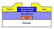
유기 박막 트랜지스터는 도 1에 나타낸 바와 같이, 게이트(gate) 전극에 전압이 인가되면 게이트 유전체층(gate dielectric layer)의 유전적 특성에 의한 국부적 분극 효과에 의해 전하가 축적되고, 축적된 전하에 의해 게이트 유전체층과 유기 반도체층(organic semiconductor) 사이에 채널이 형성되어 소스(source)와 드레인(drain) 사이에 전압이 인가되면 전하가 흐르는 구동 상태(on 상태)가 되는 반면, 게이트 전극에 0 전압 및 역전압이 인가되면 소스와 드레인 사이에 전압이 인가되더라도 전하가 흐르지 않는 비구동상태(off 상태)가 되는 원리로 디스플레이(display)와 같은 유기소자의 구동회로 역할을 한다.1, when a voltage is applied to a gate electrode, charge is accumulated by a local polarization effect due to a dielectric property of a gate dielectric layer, and the gate is accumulated by the accumulated charge. When a voltage is applied between a source and a drain because a channel is formed between the dielectric layer and the organic semiconductor layer, a driving state (on state) in which electric charge flows is generated, whereas a zero voltage and a reverse voltage are applied to the gate electrode. When a voltage is applied, it acts as a driving circuit of an organic device such as a display in a principle of being in a non-driving state (off state) in which charge does not flow even when a voltage is applied between the source and drain.
OTFTs는 flexible display, 무선 주파수 식별 태그, 메모리 및 센서와 같은 다양한 전자 장치에 적용될 수 있다. OTFTs 주요 기술은 재료 합성(유기반도체, 유전체 및 전극), 소자 제조 방법, 디바이스 물리학의 개발에 있고, 특히, 유전체 재료는 게이트 전극과 결합하여 전계 효과를 나타내어 트랜지스터 성능을 결정하는 가장 중요한 구성 요소 중 하나이다. 이러한 전계 효과는 유전체 벌크 특성(유전 상수 (κ) 및 유전체 강도)에 의해 크게 영향을 받는다.OTFTs can be applied to various electronic devices such as flexible displays, radio frequency identification tags, memory and sensors. The main technologies of OTFTs are in the synthesis of materials (derivatives, dielectrics and electrodes), device fabrication methods, and the development of device physics. In particular, dielectric materials are one of the most important components to determine transistor performance by combining with gate electrodes to exhibit field effects. It is one. This field effect is greatly influenced by the dielectric bulk properties (dielectric constant (κ) and dielectric strength).
OTFTs에 사용되는 유전체 물질은 일반적으로 무기 또는 유기 물질의 두 가지 범주로 구분된다. 무기 재료는 높은 유전 상수(κ), 강한 절연 내력 및 화학적 및 열적 저항, 저전압 작동의 우수한 유전체 특성을 가지나 무기 물질 고유의 취성, 복잡한 제조 공정, 유기 반도체와 비 호환성, 계면 트랩 유발로 인한 낮은 전하 캐리어 전송을 야기한다. 반면에, 유기 유전체 재료(특히 폴리머)는 유연하고, 유기 반도체와의 융통성, 가공성 및 상용성을 제공하지만 상대적으로 낮은 κ와 약한 물성을 가진다.The dielectric materials used in OTFTs are generally divided into two categories: inorganic or organic. Inorganic materials have high dielectric constant (κ), strong dielectric strength and chemical and thermal resistance, excellent dielectric properties of low-voltage operation, but the intrinsic brittleness of inorganic materials, complex manufacturing processes, incompatibility with organic semiconductors, low charges caused by interfacial trapping Causing carrier transmission. On the other hand, organic dielectric materials (especially polymers) are flexible and provide flexibility, processability and compatibility with organic semiconductors, but have relatively low κ and weak properties.
고성능 OTFTs에 적합한 유전체층을 만들기 위해서, 다양한 형태의 유기상과 무기상을 혼합하여 OTFTs를 제조하려는 많은 시도가 있었고, 이 중에서도 졸-겔 공정을 통한 무기-유기 나노 하이브리드 유전체의 합성은 상기 무기 및 유기 물질의 유리한 특성을 충족시킬 수 있는 유망한 후보로 알려져 있으나, 무기 및 유기 물질의 유리한 특성을 극대화하고, 핀홀이 없고, 평활하며, 게이트 누설 전류가 낮고, 기판 접착력 및 굽힘 안정성이 우수한 물성을 가지는 고성능 유전체 물질의 개발이 여전히 요구되고 있다.In order to make a dielectric layer suitable for high-performance OTFTs, many attempts have been made to prepare OTFTs by mixing various types of organic phases and inorganic phases, and among these, synthesis of inorganic-organic nano-hybrid dielectrics through a sol-gel process is the synthesis of the inorganic and organic materials. It is known as a promising candidate that can satisfy advantageous properties, but it is a high-performance dielectric material that maximizes the advantageous properties of inorganic and organic materials, has no pinholes, is smooth, has low gate leakage currents, and has excellent properties of substrate adhesion and bending stability. Development is still in demand.
본 발명은 기판 접착력과 가요성 전자 디바이스에 요구되는 굽힘 안정성이 높으며, 핀홀이 없고, 평활하여 게이트 누설 전류가 없는 고성능 OTFTs의 제조에 이용될 수 있는 새로운 무기-유기 나노 하이브리드된 게이트 유전체 조성물을 제공하는 데 그 목적이 있다.The present invention provides a novel inorganic-organic nano-hybrid gate dielectric composition that can be used in the manufacture of high-performance OTFTs with high substrate adhesion and bending stability required for flexible electronic devices, no pinholes, and smooth gate-free leakage currents. It has its purpose.
상기 목적을 달성하기 위하여, 본 발명은 하기 화학식 1의 구조로 표시되는 양친성 고분자 사슬을 가지는 다리걸친 유기실리카 전구체(APAS)를 포함하는 것을 특징으로 하는, 유기박막 트랜지스터용 게이트 유전체 조성물을 제공한다.To achieve the above object, the present invention provides a gate dielectric composition for an organic thin film transistor, characterized in that it comprises a bridged organosilica precursor (APAS) having an amphiphilic polymer chain represented by the structure of
[화학식 1][Formula 1]

(상기 화학식 1에서,(In the
상기 A는 폴리프로필렌 트리올 또는 글리세롤로서, 상기 B의 이소시아네이트기와 반응하여 우레탄 결합이 형성되고;The A is polypropylene triol or glycerol, and reacts with the isocyanate group of B to form a urethane bond;
상기 B는 디이소시아네이트 화합물로서, 하나의 이소시아이트기는 상기 A의 히드록시기와 반응하여 우레탄 결합이 형성되고, 다른 하나는 상기 C의 히드록시기와 반응하여 우레탄 결합이 형성되거나, 상기 D의 히드록시기와 반응하여 우레탄 결합이 형성되고;The B is a diisocyanate compound, one isocyanate group reacts with the hydroxyl group of A to form a urethane bond, and the other reacts with the hydroxyl group of C to form a urethane bond or react with the hydroxyl group of D. To form a urethane bond;
상기 C는 히드록시기 또는 아민기를 포함하는 알콕시실란으로서, 히드록시기 또는 아민기는 상기 B의 이소시아네이트기와 반응하여 우레탄 결합 또는 우레아 결합이 형성되고;C is an alkoxysilane containing a hydroxy group or an amine group, and the hydroxy group or amine group reacts with the isocyanate group of B to form a urethane bond or a urea bond;
상기 D는 폴리에틸렌 글리콜로서, 히드록시기는 상기 B의 이소시아네이트기와 반응하여 우레탄 결합이 형성됨.)The D is polyethylene glycol, and the hydroxyl group reacts with the isocyanate group of B to form a urethane bond.)
본 발명에 따른 유기박막 트랜지스터용 게이트 유전체 조성물은 티타늄 알콕사이드 화합물, 바람직하게는 티타늄 테트라키스이소프로폭사이드(TTIP)를 더 포함할 수 있다.The gate dielectric composition for an organic thin film transistor according to the present invention may further include a titanium alkoxide compound, preferably titanium tetrakisisopropoxide (TTIP).
본 발명에 따른 유기박막 트랜지스터용 게이트 유전체 조성물은 실리콘 알콕사이드 화합물, 바람직하게는 테트라에틸오르토실리케이트(TEOS) 또는 프로필트리메톡시실란(PTMS)을 더 포함할 수 있다.The gate dielectric composition for an organic thin film transistor according to the present invention may further include a silicon alkoxide compound, preferably tetraethyl orthosilicate (TEOS) or propyltrimethoxysilane (PTMS).
본 발명에 따른 유기박막 트랜지스터용 게이트 유전체 조성물은 글리시독시 실란 화합물, 바람직하게는 (3-글리시독시프로필)트리메톡시실란(GPTMS) 또는 (3-글리시독시프로필)트리에톡시실란을 더 포함할 수 있다.The gate dielectric composition for an organic thin film transistor according to the present invention comprises a glycidoxy silane compound, preferably (3-glycidoxypropyl) trimethoxysilane (GPTMS) or (3-glycidoxypropyl) triethoxysilane It may further include.
본 발명에 따라 제조된 유기박막 트랜지스터용 게이트 유전체 조성물은 양친성 고분자 사슬을 가지는 다리걸친 유기실리카 전구체(APAS)를 이용함으로써 기판 접착력이 현저히 개선될 뿐 아니라, 가요성 기판에 요구되는 광 투과도, 굽힘(bending) 안정성이 매우 우수하며, 핀홀이 없고, 평활하여 게이트 누설 전류가 없어 고성능 OTFTs의 제조에 유용하게 이용될 수 있다.The gate dielectric composition for an organic thin film transistor manufactured according to the present invention not only significantly improves substrate adhesion by using a bridged organosilica precursor (APAS) having an amphiphilic polymer chain, but also transmits light and bends required for a flexible substrate. (bending) It has very good stability, no pinhole, and no smooth gate leakage current, so it can be usefully used for manufacturing high-performance OTFTs.
도 1은 유기 박막 트랜지스터의 개략적인 구조를 나타낸 도면이다.
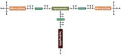
도 2는 본 발명에 따른 양친성 고분자 사슬을 가지는 다리걸친 유기실리카 전구체(APAS)의 다이어그램이다.
도 3은 본 발명에 따른 양친성 고분자 사슬을 가지는 다리걸친 유기실리카 전구체(APAS)를 포함하는 게이트 유전체 조성물(AGPTi)와 APAS를 포함하지 않는 게이트 유전체 조성물(GPTi)를 1개월 간 냉장 보관 후 저장 안정성을 나타내는 사진이다.
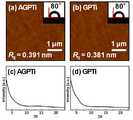
도 4의 (a)는 AGPTi의 AFM 이미지, (b)는 GPTi의 AFM 이미지, (c)는 AGPTi의 XRD 분석 결과, (d)는 GPTi의 XRD 분석 결과이다.
도 5의 (a)는 UV-가시 투과율 스펙트럼, (b)는 실시예에 따른 AGPTi 필름 표면의 FE-SEM 이미지, (c)는 비교예에 따른 GPTi 필름 표면의 FE-SEM 이미지이다.
도 6은 온도에 따른 졸-겔 막 특성의 변화를 모니터링하기 위해 실시예의 게이트 유전체 조성물(AGPTi)와 APAS를 포함하지 않는 비교예의 게이트 유전체 조성물(GPTi) 필름에 대한 열 중량 분석(TGA) 결과이다.
도 7의 (a)는 실시예에 따른 AGTPi와 비교예에 따른 GPTi의 유전율(Dielectric constant), (b)는 전기장에 따른 누설전류밀도(Leakage current density)를 나타내는 그래프이다.
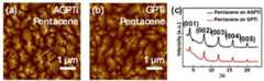
도 8의 (a)는 실시예에 따른 AGPTi 유전체 상에 진공 증착된 펜타센 필름의 표면형상 이미지, (b)는 비교예에 따른 GPTi 유전체 상에 진공 증착된 펜타센 필름의 표면형상 이미지, (c)는 AGPTi 유전체와 GPTi 유전체 상에 진공 증착된 펜타센 필름의 X-선 회절분석(XRD) 결과이다.
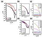
도 9는 Si 기판 상에 제조된 펜타센 전계효과 트랜지스터(Field Effect Transistor, FET)의 전달 및 출력 특성을 나타낸 것으로, (a)는 실시예의 AGPTi 유전체와 비교예의 GPTi 유전체가 도입된 OFET(Oranic FET)에서 전달 특성(게이트 전압(VG)-드레인 전류(ID) curve), (b)는 AGPTi의 전달 특성(VG-ID curve), (c)는 AGPTi의 출력 특성(VD-ID curve), (d)는 GPTi의 전달 특성(VG-ID curve), (e)는 GPTi의 출력 특성(VD-ID curve)을 나타내는 그래프이다.
도 10은 본 발명에 따른 AGPTi와 비교예의 GPTi의 PET 기판에 대한 접착 및 굽힘 특성을 나타내는 것으로, (a)는 순수한 PET 필름의 AFM 이미지, (b)는 굽힘(bending) 곡률 반경(r=5.5 mm), (c)는 AGPTi 기판과 GPTi 기판의 100회 굽힘 시험 전후 사진, (d)는 굽힘 시험 전후 AFM 이미지이다.
도 11은 곡률반경 R = 5.5mm 에서 30회 굽힘 전후 AGPTi, GPTi 각 막의 MIM 구조 캐패시터의 게이트 누설 전류를 나타내는 그래프이다.
도 12의 (a)는 제작된 가요성 FET의 개략도, (b)는 굽힘 곡률 반경(r=5.5 mm), (c)는 실시예 4(AGPTi)에 따른 OTFT의 전달 특성(VG-ID curve), (d)는 비교예 3(GPTi)에 따른 OTFT의 전달 특성(VG-ID curve), (e)는 실시예 4에 따른 OTFT의 굽힘 횟수에 따른 드레인 전류 안정성, (f)는 비교예 3에 따른 OTFT의 굽힘 횟수에 따른 드레인 전류 안정성을 나타내는 그래프이다.1 is a view showing a schematic structure of an organic thin film transistor.
2 is a diagram of a bridged organosilica precursor (APAS) having an amphiphilic polymer chain according to the present invention.
FIG. 3 shows a gate dielectric composition (AGPTi) containing a bridged organosilica precursor (APAS) having an amphiphilic polymer chain according to the present invention and a gate dielectric composition (GPTi) not containing APAS after being refrigerated for 1 month and stored. This is a picture showing stability.
4(a) is an AFM image of AGPTi, (b) is an AFM image of GPTi, (c) is an XRD analysis result of AGPTi, and (d) is an XRD analysis result of GPTi.
5 (a) is a UV-visible transmittance spectrum, (b) is an FE-SEM image of the AGPTi film surface according to the embodiment, (c) is a FE-SEM image of the GPTi film surface according to the comparative example.
FIG. 6 is a thermogravimetric analysis (TGA) result of a gate dielectric composition (AGPTi) of an example and a gate dielectric composition (GPTi) film of a comparative example not containing APAS to monitor changes in sol-gel film properties with temperature. .
7 (a) is a dielectric constant (dielectric constant) of the GPTP according to the example and AGTPi according to the embodiment, (b) is a graph showing the leakage current density (Leakage current density) according to the electric field.
8(a) is a surface shape image of a pentacene film vacuum-deposited on an AGPTi dielectric according to an embodiment, (b) is a surface shape image of a pentacene film vacuum-deposited on a GPTi dielectric according to a comparative example, ( c) is an X-ray diffraction analysis (XRD) result of a pentacene film vacuum-deposited on the AGPTi dielectric and GPTi dielectric.
FIG. 9 shows transfer and output characteristics of a pentacene field effect transistor (FET) fabricated on a Si substrate. (a) is an OFET (Oranic FET) in which the AGPTi dielectric of the embodiment and the GPTi dielectric of the comparative example are introduced. ), transfer characteristics (gate voltage (VG )-drain current (ID ) curve), (b) AGPTi transfer characteristics (VG -ID curve), (c) AGPTi output characteristics (VD- ID curve), (d) are GPTi transfer characteristics (VG -ID curve), and (e) are graphs showing GPTi output characteristics (VD -ID curve).
FIG. 10 shows the adhesion and bending properties of AGPTi and GPTi of Comparative Example to a PET substrate according to the present invention, (a) is an AFM image of a pure PET film, and (b) is a bending radius of curvature (r=5.5). mm), (c) are photographs before and after the 100-time bending test of the AGPTi substrate and GPTi substrate, and (d) are AFM images before and after the bending test.
11 is a graph showing the gate leakage current of the MIM structure capacitors of AGPTi and GPTi films before and after bending 30 times at a radius of curvature R = 5.5 mm.
12(a) is a schematic diagram of the fabricated flexible FET, (b) is a bending radius of curvature (r=5.5 mm), and (c) is a transfer characteristic (VG -I of OTFT) according to Example 4 (AGPTi)D curve), (d) is the transfer characteristic of the OTFT according to Comparative Example 3 (GPTi) (VG -ID curve), (e) is the drain current stability according to the number of bending times of the OTFT according to Example 4, (f ) Is a graph showing the drain current stability according to the number of bending of the OTFT according to Comparative Example 3.
본 발명자는 소수성 세그먼트와 친수성 세그먼트를 동시에 가지면서 양 말단에 알콕시 실란기를 가지는 신규한 양친성 고분자 사슬을 가지는 다리걸친 유기실리카 전구체를 합성하여 Amphiphilic Polymeric Alkoxy Silane의 약어인 'APAS'로 명명하고, 상기 신규 화합물을 대한민국 특허공개 제10-2012-0106357호에 개시하였다.The present inventor synthesizes a bridged organosilica precursor having a novel amphiphilic polymer chain having an alkoxy silane group at both ends while simultaneously having a hydrophobic segment and a hydrophilic segment. The new compound is disclosed in Korean Patent Publication No. 10-2012-0106357.
본 발명은 상기 합성된 양친성 고분자 사슬을 가지는 다리걸친 유기실리카 전구체(이하 'APAS' 또는 'APAS 전구체')를 포함하는 조성물의 유기박막 트랜지스터 제조용 게이트 유전체로서의 신규한 용도를 개시한다.The present invention discloses a novel use of a composition comprising a bridged organosilica precursor (hereinafter'APAS' or'APAS precursor') having the synthesized amphiphilic polymer chain as a gate dielectric for manufacturing an organic thin film transistor.
본 발명자들은 상기 합성된 APAS 전구체를 유효성분으로 하는 졸-겔 반응 조성물을 Si 기판이나 가요성 고분자 기판에 스핀 코팅한 후, 어닐링 처리한 결과, 기판 접착 특성이 현저히 우수할 뿐 아니라, 광 투과도, 굽힘(bending) 안정성이 우수하며, 상기 졸-겔 반응 조성물은 게이트 유전체층으로 하고 펜타센을 유기 반도체물질로 하여 유기 분자 빔 증착을 통해 OTFTs를 제조한 결과, 핀홀이 없고, 평활하여 게이트 누설 전류가 없는 고성능 OTFTs의 제조가 제조됨을 확인함으로써 본 발명을 완성하였다.The present inventors spin-coated the sol-gel reaction composition using the synthesized APAS precursor as an active ingredient on a Si substrate or a flexible polymer substrate, and after annealing, the substrate adhesion properties are not only excellent, but also light transmittance, The bending stability is excellent, and the sol-gel reaction composition is a gate dielectric layer, and OTFTs are produced through organic molecular beam deposition using pentacene as an organic semiconductor material. As a result, there is no pinhole, and the gate leakage current is smooth. The present invention was completed by confirming that the manufacture of high-performance OTFTs without them was made.
본 발명에 따른 OTFTs용 게이트 유전체 조성물은 양친성 고분자 사슬을 가지는 다리걸친 유기실리카 전구체(APAS), 티타늄 알콕사이드 화합물, 실리콘 알콕사이드 화합물, 글리시독시 실란 화합물을 포함하여, 가수분해 및 축합 반응의 졸-겔 공정을 통해 APAS 전구체의 유기 성분과 SiO2-TiO2 의 무기 성분이 하이브리드된 망목 구조를 통하여 기판에 대한 강력한 접착 특성 뿐 아니라 우수한 가요성 특성을 나타내는 게이트 유전체로서의 역할을 수행한다.The gate dielectric composition for OTFTs according to the present invention includes a bridged organosilica precursor (APAS) having an amphiphilic polymer chain, a titanium alkoxide compound, a silicon alkoxide compound, and a glycidoxy silane compound, solubilizing the hydrolysis and condensation reaction. Through the gel process, the organic component of the APAS precursor and the inorganic component of SiO2 -TiO2 are used as a gate dielectric that exhibits excellent flexibility characteristics as well as strong adhesion properties to the substrate through a hybrid network structure.
본 발명에 있어서, 상기 APAS 전구체, 티타늄 알콕사이드 화합물, 실리콘 알콕사이드 화합물 및 글리시독시 실란 화합물로 이루어진 전구체 조성물 또는 상기 전구체들의 졸-겔 반응된 화합물을 'AGTPi'로 명명하고, 비교예에서 본 발명에 따른 상기 APAS 전구체 없이, 티타늄 알콕사이드 화합물, 실리콘 알콕사이드 화합물 및 글리시독시 실란 화합물로 이루어진 전구체 조성물 또는 상기 전구체들의 졸-겔 반응된 화합물을 'GTPi'로 명명한다.In the present invention, the precursor composition composed of the APAS precursor, the titanium alkoxide compound, the silicon alkoxide compound, and the glycidoxy silane compound, or the sol-gel reacted compound of the precursors is named'AGTPi', and in the comparative example, Without the APAS precursor according to the precursor composition consisting of a titanium alkoxide compound, a silicon alkoxide compound and a glycidoxy silane compound or a sol-gel reacted compound of the precursors is referred to as'GTPi'.
먼저, 본 발명에 따른 APAS 전구체는 하기 화학식 1에 보이는 바와 같이 A, B, C, D의 네 종류 물질이 화학 결합된 구조로, 소수성 세그먼트(A 부분)와 친수성 세그먼트(D 부분)를 동시에 가지는 일종의 실란 화합물(C 부분)이다.First, the APAS precursor according to the present invention has a structure in which four kinds of materials A, B, C, and D are chemically bonded as shown in Chemical Formula 1, and simultaneously has a hydrophobic segment (A part) and a hydrophilic segment (D part). It is a kind of silane compound (C part).
[화학식 1][Formula 1]

(상기 화학식 1에서,(In the
상기 A는 폴리프로필렌 트리올 또는 글리세롤로서, 상기 B의 이소시아네이트기와 반응하여 우레탄 결합이 형성되고;The A is polypropylene triol or glycerol, and reacts with the isocyanate group of B to form a urethane bond;
상기 B는 디이소시아네이트 화합물로서, 하나의 이소시아이트기는 상기 A의 히드록시기와 반응하여 우레탄 결합이 형성되고, 다른 하나는 상기 C의 히드록시기와 반응하여 우레탄 결합이 형성되거나, 상기 D의 히드록시기와 반응하여 우레탄 결합이 형성되고;The B is a diisocyanate compound, one isocyanate group reacts with the hydroxyl group of A to form a urethane bond, and the other reacts with the hydroxyl group of C to form a urethane bond or react with the hydroxyl group of D. To form a urethane bond;
상기 C는 히드록시기 또는 아민기를 포함하는 알콕시실란으로서, 히드록시기 또는 아민기는 상기 B의 이소시아네이트기와 반응하여 우레탄 결합 또는 우레아 결합이 형성되고;C is an alkoxysilane containing a hydroxy group or an amine group, and the hydroxy group or amine group reacts with the isocyanate group of B to form a urethane bond or a urea bond;
상기 D는 폴리에틸렌 글리콜로서, 히드록시기는 상기 B의 이소시아네이트기와 반응하여 우레탄 결합이 형성됨.)The D is polyethylene glycol, and the hydroxyl group reacts with the isocyanate group of B to form a urethane bond.)
도 2는 상기 화학식 1의 물질 간 결합 구조를 나타내는 다이어그램이다.2 is a diagram showing a bonding structure between substances of
도 2를 참조하여 상기 화학식 1을 설명하면,Referring to the formula (1) with reference to Figure 2,
상기 A는 소수성 세그먼트를 가지는 물질로, 폴리프로필렌 트리올 또는 글리세롤이며, 각각의 히드록시기는 이소시아네이트기와 반응하여 우레탄 결합을 형성한다. 상기 폴리프로필렌 트리올의 평균 분자량은 바람직하게는 260 ~ 2,000 g/mol, 더욱 바람직하게는 1,000 g/mol이다.The A is a material having a hydrophobic segment, polypropylene triol or glycerol, and each hydroxy group reacts with an isocyanate group to form a urethane bond. The average molecular weight of the polypropylene triol is preferably 260 to 2,000 g/mol, more preferably 1,000 g/mol.
상기 B는 A와 C, A와 D를 매개하는 역할로서 디이소시아네이트 물질이다. 하나의 이소시아네이트기는 상기 A의 히드록시기와, 또 다른 이소시아네이트기는 상기 C 또는 D의 히드록시기와 우레탄 결합을 형성하거나 상기 C의 아민기와 우레아 결합을 형성한다. 상기 디이소시아네이트는 톨루엔 디이소시아네이트(TDI), 이소포론 디이소시아네이트, 메틸렌 디이소시아네이트, 메틸렌 디페닐 디이소시아네이트, 헥사메틸렌 디이소시아네이트, 크실렌 디이소시아네이트, 톨리딘 디이소시아네이트 등 우레탄 합성에 사용되는 물질이면 모두 적용될 수 있다.The B is a diisocyanate material that mediates A and C, A and D. One isocyanate group forms a urethane bond with the hydroxy group of A and another hydroxy group of C or D, or forms a urea bond with the amine group of C. The diisocyanate can be applied to any material used in the synthesis of urethane, such as toluene diisocyanate (TDI), isophorone diisocyanate, methylene diisocyanate, methylene diphenyl diisocyanate, hexamethylene diisocyanate, xylene diisocyanate, tolidine diisocyanate. have.
상기 C는 히드록시기 또는 아민기를 가지는 알콕시실란으로서, 상기 히드록시기인 경우 상기 B의 이소시아네이트기와 우레탄 결합을 형성하고, 상기 아민기인 경우 상기 B의 이소시아네이트기와 우레아 결합을 형성한다. 본 발명의 게이트 유전체 특성 발현시 상기 C의 알콕시실란기는 가수분해-응축반응을 통해 티타늄 알콕사이드 화합물, 실리콘 알콕사이드 화합물과 서로 가교되어 네트워크 구조체를 형성하게 된다.The C is an alkoxysilane having a hydroxy group or an amine group, and in the case of the hydroxy group, forms an urethane bond with the isocyanate group of the B, and forms an urea bond with the isocyanate group of the B in the case of the amine group. When expressing the gate dielectric properties of the present invention, the alkoxysilane group of C is cross-linked with a titanium alkoxide compound and a silicon alkoxide compound through a hydrolysis-condensation reaction to form a network structure.
상기 D는 수분산성을 위한 친수성 세그먼트를 가지는 것으로, 폴리에틸렌글리콜이 이용되며, 히드록시기는 상기 B의 이소시아네이트기와 우레탄 결합을 형성한다. 상기 폴리에틸렌 글리콜의 평균 분자량은 600 내지 15,000 g/mol인 것이 바람직하다.The D has a hydrophilic segment for water dispersibility, polyethylene glycol is used, and the hydroxy group forms a urethane bond with the isocyanate group of the B. The polyethylene glycol preferably has an average molecular weight of 600 to 15,000 g/mol.
본 발명에 적용될 수 있는 A, B, C, D 의 대표 물질을 하기 표 1에 나타내었다.Representative materials of A, B, C, and D that can be applied to the present invention are shown in Table 1 below.
AA

m=1~50, n=0~50, p=0~50
m=1~50, n=0~50, p=0~50
BB

2-6-톨루엔 디이소시아네이트2,4-toluene diisocyanate,
2-6-toluene diisocyanate


CC


DD
상기 화학식 1과 같은 구조를 가지는 유기실리카 전구체의 합성은 다음과 같은 공정을 통해 수행된다.Synthesis of the organosilica precursor having the structure of
양친성 고분자 사슬을 가지는 다리걸친 유기실리카 전구체(APAS)의 합성Synthesis of bridged organosilica precursors (APAS) with amphiphilic polymer chains
제1단계:Step 1:
질소 분위기 하에서, 소수성 세그먼트와 3개 이상의 히드록시기를 가지는 물질 A(폴리프로필렌 트리올)와, 2개 이상의 이소시아네이트기를 가지는 물질 B(디이소시아네이트)를 1:3의 반응 몰비로 하여서 45 ~ 50 ℃에서 4시간 동안 교반 반응시켜 A, B 간에 우레탄 결합을 형성시킨다.Under nitrogen atmosphere, at a reaction molar ratio of 1:3, the hydrophobic segment, the substance A (polypropylene triol) having three or more hydroxy groups, and the substance B (diisocyanate) having two or more isocyanate groups are 4 at 45 to 50°C. The reaction was stirred for a time to form urethane bonds between A and B.
제2단계:Step 2:
상기 제1단계에서 얻어진 합성물에 히드록시기 또는 아민기를 가지는 알콕시실란(C)를 첨가하여 50 ~ 55 ℃에서 반응시켜 B, C 간에 우레탄 또는 우레아 결합을 형성시킨다. 상기 제1 단계의 합성물과 물질 C의 반응 몰비는 1:2로 한다.An alkoxysilane (C) having a hydroxy group or an amine group is added to the composite obtained in the first step to react at 50 to 55° C. to form urethane or urea bonds between B and C. The reaction molar ratio of the compound of the first step and the material C is 1:2.
제3단계:Step 3:
상기 제2단계에서 얻어진 합성물에 친수성 세그먼트와 히드록시기를 가지는 물질 D, 바람직하게는 분자량이 600 ~ 15,000인 폴리에틸렌옥시드를 1몰비로 첨가하여 교반 반응시켜 B, D 간에 우레탄 결합을 형성시켜 본 발명의 양친성 고분자 사슬을 가지는 다리걸친 유기실리카 전구체(APAS)를 합성한다.In the composite obtained in the second step, a material having a hydrophilic segment and a hydroxyl group D, preferably polyethylene oxide having a molecular weight of 600 to 15,000 is added in a 1 molar ratio and stirred to form a urethane bond between B and D to form a urethane bond of the present invention. A bridged organosilica precursor (APAS) having an amphiphilic polymer chain is synthesized.
본 발명에 따른 OTFTs용 게이트 유전체 조성물은 무기 성분으로 TiO2 결합을 위하여 티타늄 알콕사이드(Titanium alkoxide) 화합물을 더 포함할 수 있다. 상기 티타늄 알콕사이드 화합물로는 티타늄 테트라키스이소프로폭사이드(TTIP)이 바람직하나, TiO2 결합을 제공할 수 있는 공지된 티타늄 알콕사이드 화합물이면 모두 포함될 수 있다.The gate dielectric composition for OTFTs according to the present invention may further include a titanium alkoxide compound for TiO2 bonding as an inorganic component. The titanium alkoxide compound is preferably titanium tetrakisisopropoxide (TTIP), but any known titanium alkoxide compound capable of providing a TiO2 bond may be included.
본 발명에 따른 OTFTs용 게이트 유전체 조성물은 무기 성분으로 SiO2 결합을 위하여 실리콘 알콕사이드(silicon alkoxide) 화합물을 더 포함할 수 있다. 상기 실리콘 알콕사이드 화합물로는 테트라에틸오르토실리케이트(TEOS) 또는 프로필트리메톡시실란(PTMS)이 바람직하나, SiO2 결합을 제공할 수 있는 공지된 실리콘 알콕사이드 화합물이면 모두 포함될 수 있다.The gate dielectric composition for OTFTs according to the present invention may further include a silicon alkoxide compound for SiO2 bonding as an inorganic component. As the silicon alkoxide compound, tetraethyl orthosilicate (TEOS) or propyltrimethoxysilane (PTMS) is preferred, but any known silicon alkoxide compound capable of providing an SiO2 bond may be included.
상기 접착제 조성물은 양친성 고분자 사슬을 가지는 다리걸친 유기실리카 전구체(APAS) 10~40 중량%, 티타늄 알콕사이드 화합물 10~40 중량%, 실리콘 알콕사이드 화합물 10~40 중량%, 글리시독시 실란 화합물 10~40 중량%로 이루어질 수 있으나, 이에 제한되지는 않는다.The adhesive composition is 10-40% by weight of a bridged organosilica precursor (APAS) having an amphiphilic polymer chain, 10-40% by weight of a titanium alkoxide compound, 10-40% by weight of a silicon alkoxide compound, 10-40 of glycidoxy silane compound It may be made of weight%, but is not limited thereto.
본 발명에 따른 OTFTs용 게이트 유전체 조성물은 무기 성분으로 SiO2 결합을 위하여 글리시독시 실란(glycidoxy silane) 화합물을 더 포함할 수 있다. 상기 글리시독시 실란 화합물로는 (3-글리시독시프로필)트리메톡시실란(GPTMS) 또는 (3-글리시독시프로필)트리에톡시실란이 바람직하나, 이에 제한되지는 않는다.The gate dielectric composition for OTFTs according to the present invention may further include a glycidoxy silane compound for SiO2 bonding as an inorganic component. The glycidoxy silane compound is preferably (3-glycidoxypropyl) trimethoxysilane (GPTMS) or (3-glycidoxypropyl) triethoxysilane, but is not limited thereto.
한편, 본 발명은 기판, 게이트 전극, 게이트 유전체층, 유기 반도체층, 소스/드레인 전극 및 소스와 드레인 전극을 포함하고,Meanwhile, the present invention includes a substrate, a gate electrode, a gate dielectric layer, an organic semiconductor layer, a source/drain electrode, and a source and drain electrode,
상기 게이트 유전체층은 하기 화학식 1의 구조로 표시되는 양친성 고분자 사슬을 가지는 다리걸친 유기실리카 전구체(APAS)를 포함하여 졸-겔 반응된 조성물인 것을 특징으로 하는, 유기박막 트랜지스터를 제공한다.The gate dielectric layer is a sol-gel reacted composition comprising a bridged organosilica precursor (APAS) having an amphiphilic polymer chain represented by the structure of
[화학식 1][Formula 1]

(상기 화학식 1에서,(In the
상기 A는 폴리프로필렌 트리올 또는 글리세롤로서, 상기 B의 이소시아네이트기와 반응하여 우레탄 결합이 형성되고;The A is polypropylene triol or glycerol, and reacts with the isocyanate group of B to form a urethane bond;
상기 B는 디이소시아네이트 화합물로서, 하나의 이소시아이트기는 상기 A의 히드록시기와 반응하여 우레탄 결합이 형성되고, 다른 하나는 상기 C의 히드록시기와 반응하여 우레탄 결합이 형성되거나, 상기 D의 히드록시기와 반응하여 우레탄 결합이 형성되고;The B is a diisocyanate compound, one isocyanate group reacts with the hydroxyl group of A to form a urethane bond, and the other reacts with the hydroxyl group of C to form a urethane bond or react with the hydroxyl group of D. To form a urethane bond;
상기 C는 히드록시기 또는 아민기를 포함하는 알콕시실란으로서, 히드록시기 또는 아민기는 상기 B의 이소시아네이트기와 반응하여 우레탄 결합 또는 우레아 결합이 형성되고;C is an alkoxysilane containing a hydroxy group or an amine group, and the hydroxy group or amine group reacts with the isocyanate group of B to form a urethane bond or a urea bond;
상기 D는 폴리에틸렌 글리콜로서, 히드록시기는 상기 B의 이소시아네이트기와 반응하여 우레탄 결합이 형성됨.)The D is polyethylene glycol, and the hydroxyl group reacts with the isocyanate group of B to form a urethane bond.)
상기 기판은 Si 웨이퍼는 물론, 가요성을 가지는 공지된 재료를 모두 포함한다.The substrate includes not only Si wafers, but also all known materials having flexibility.
상기 게이트 전극, 소스/드레인 전극은 전류를 통하는 재료이고, OTFT에 이용되는 공지의 전극 재료는 모두 포함될 수 있다.The gate electrode and the source/drain electrodes are materials for conducting current, and any known electrode materials used for OTFT may be included.
상기 유기 반도체층 펜타센, TES-ADT 등 OTFT에 이용되는 공지의 유기 반도체 재료는 모두 포함될 수 있다.All known organic semiconductor materials used in OTFT, such as the organic semiconductor layer pentacene and TES-ADT, may be included.
이하 실시예를 통하여 본 발명의 OTFTs용 게이트 유전체 조성물을 상세히 설명한다.Hereinafter, a gate dielectric composition for OTFTs of the present invention will be described in detail through examples.
실시예 1. APAS 전구체의 합성Example 1. Synthesis of APAS precursors
유리 반응기의 잔류 수분을 제거하기 위해 10분 동안 질소 가스 주입한 후, 디부틸주석 딜라우레이트(DBTDL, Aldrich Chemical Co.) 촉매 0.1 중량%를 함유하는 이소포론 디이소시아네이트(IPDI, Junsei Chemical Co.) 0.3몰을 반응기에 넣은 후 폴리프로필렌글리콜(PPG, Mw=425 g/mol, Aldrich Chemical Co.) 0.1몰을 실온에서 30분 동안 적가하고, 45 ~ 50 ℃에서 4시간 동안 교반 반응시켰다.Isophorone diisocyanate (IPDI, Junsei Chemical Co.) containing 0.1% by weight of a dibutyltin dilaurate (DBTDL, Aldrich Chemical Co.) catalyst after 10 minutes of nitrogen gas injection to remove residual moisture in the glass reactor. ) 0.3 mol was added to the reactor and then 0.1 mol of polypropylene glycol (PPG, Mw=425 g/mol, Aldrich Chemical Co.) was added dropwise at room temperature for 30 minutes, followed by stirring at 45 to 50°C for 4 hours.
상기 얻어진 합성물에 (3-아미노프로필)트리에톡시실란(APTES, Aldrich Chemical Co.) 0.2몰을 첨가하고 55 ℃에서 8시간 반응시켜 에톡시실란기가 도입된 전구체를 합성하였다.0.2 mol of (3-aminopropyl) triethoxysilane (APTES, Aldrich Chemical Co.) was added to the obtained composite and reacted at 55° C. for 8 hours to synthesize a precursor into which ethoxysilane groups were introduced.
상기 에톡시실란기가 도입된 합성물에 폴리에틸렌글리콜(PEG, Mw=300 g/mol, Aldrich Chemical Co.) 0.1몰 첨가하여 교반 반응시켜 양친성 고분자 사슬을 가지는 다리걸친 유기실리카 전구체(APAS)를 합성한다.0.1 mol of polyethylene glycol (PEG, Mw=300 g/mol, Aldrich Chemical Co.) was added to the ethoxysilane group-incorporated compound, followed by stirring to synthesize a bridged organosilica precursor (APAS) having amphiphilic polymer chains. .
반응 종말점은 FT-IR 분광측정기(iS5, Thermo Fisher Scientific, USA)을 통해 2270 cm-1에서 NCO 피크가 사라지는 것으로 결정되었다. 1700 cm-1(COO stretching) 및 1078 cm-1(Si-O-Si stretching)의 피크는 APAS의 실록산 결합에 기인하는 것으로, 에톡시실란기가 APAS에 혼입되어 있음을 시사한다 (Kuo et al., 2002; Park et al., 2002). APAS의 평균 분자량은 삼중 검출(RI, UV 및 ELSD)이 가능한 EcoSEC GPC SYSTEM 기기를 사용하여 측정한 결과 1370 g/mol이었다.The reaction endpoint was determined to disappear the NCO peak at 2270 cm-1 through an FT-IR spectrometer (iS5, Thermo Fisher Scientific, USA). The peaks of 1700 cm-1 (COO stretching) and 1078 cm-1 (Si-O-Si stretching) are due to the siloxane bonds of APAS, suggesting that ethoxysilane groups are incorporated into APAS (Kuo et al. , 2002; Park et al., 2002). The average molecular weight of APAS was 1370 g/mol when measured using an EcoSEC GPC SYSTEM instrument capable of triple detection (RI, UV and ELSD).
실시예Example 2. AGTPi의 제조 2. Preparation of AGTPi
실시예 1에서 합성된 APAS 전구체 5g, (3-글리시딜옥시프로필)트리메톡시실란(GPTMS, Aldrich Chemical Co.) 5g, 프로필트리메톡시실란(PTMS, 97 %, Aldrich Chemical Co.) 5g, 티타늄(IV)이소프로폭사이드(TTiP, 97 %, Aldrich Chemical Co.) 5g을 에탄올 40g에 용해시키고, 0.1M HCl 수용액 (1.5g; H2O/Si=1, H2O/Ti=1)을 가하고 60 ℃에서 48 시간 동안 부드럽게 교반하여 가수 분해 및 트리에톡시실란기와 트리메톡시실란기의 축합 반응을 수행하여 졸-겔 반응시켰다.5 g of APAS precursor synthesized in Example 1, 5 g of (3-glycidyloxypropyl) trimethoxysilane (GPTMS, Aldrich Chemical Co.), 5 g of propyl trimethoxysilane (PTMS, 97%, Aldrich Chemical Co.) , Titanium (IV) isopropoxide (TTiP, 97%, Aldrich Chemical Co.) 5 g was dissolved in 40 g of ethanol, 0.1 M HCl aqueous solution (1.5 g; H2 O/Si=1, H2 O/Ti= 1) was added and stirred gently at 60° C. for 48 hours to perform hydrolysis and condensation reaction of triethoxysilane group and trimethoxysilane group to perform a sol-gel reaction.
실시예Example 3. AGPTi를 이용한 Si 기판 OTFTs의 제조 3. Preparation of Si substrate OTFTs using AGPTi
N형(100) 실리콘(Si) 웨이퍼를 기판(substrate)으로 사용하였다. Si 웨이퍼는 먼저 피라니아 용액, 30 분 동안의 초음파 처리 및 30 분 동안 UV-오존 노출에 의해 세척되었다.An N-type (100) silicon (Si) wafer was used as a substrate. The Si wafer was first washed by piranha solution, sonication for 30 minutes and UV-ozone exposure for 30 minutes.
금속 섀도우 마스크를 이용하여 알루미늄(Al)을 열적 증발시켜 Si 웨이퍼 상에 50 nm 두께의 Al 게이트 전극을 형성시켰다.Aluminum (Al) was thermally evaporated using a metal shadow mask to form a 50 nm thick Al gate electrode on the Si wafer.
AGPTi 혼합물(마스터 용액)을 프로필렌메틸글리콜에테르(PGME)에 용해시키고, 주위 공기 중에서 24 시간 동안 격렬하게 교반하여 졸-겔 반응시킨 다음, 상기 유리 기판 위에 3000 rpm으로 60 초간 스핀 코팅하고 100 ℃에서 30 분간 어닐링 처리하여 게이트 유전체층을 형성시켰다.The AGPTi mixture (master solution) was dissolved in propylene methyl glycol ether (PGME), stirred vigorously for 24 hours in ambient air, and subjected to a sol-gel reaction, and then spin coated at 3000 rpm for 60 seconds on the glass substrate at 100°C. An annealing treatment was performed for 30 minutes to form a gate dielectric layer.
유기 분자 빔 증착(OMBD) (증착 속도 = 0.1Å/s, 진공 압력=10-6Torr, 기판 온도= 25 ℃)을 사용하여 펜타센(pentacene, Sigma Aldrich Co.)을 게이트 유전체층 상에 증착시켜 유기 반도체층을 형성시켰다.Organic molecular beam deposition (OMBD) (deposition rate = 0.1Å / s, vacuum pressure = 10-6 Torr, substrate temperature = 25 ℃) using the vapor-deposited pentacene (pentacene, Sigma Aldrich Co.) on the gate dielectric layer An organic semiconductor layer was formed.
금속 쉐도우 마스크를 이용하여 금(Au)을 열적 증발시켜 상기 펜타센 층 상에 100 nm 두께의 Au 전극을 형성시킴으로써 상부 접촉 전극 OTFT를 제조하였다. 채널 길이(L) 및 폭(W)은 각각 150 및 1500 ㎛이었다.The upper contact electrode OTFT was prepared by thermally evaporating gold (Au) using a metal shadow mask to form a 100 nm thick Au electrode on the pentacene layer. The channel length (L) and width (W) were 150 and 1500 μm, respectively.
실시예Example 4. AGPTi를 이용한 PET 기판 OTFTs의 제조 4. Preparation of PET substrate OTFTs using AGPTi
상기 실시예 3과 동일하게 실시하되, 유리 기판 대신 가요성이 있는 PET 기판을 이용하여 OTFT를 제조하였다. 사용된 PET 기판은 3분 동안 이소프로판올(IPA)로 먼저 세척하고 10 분 동안 UV-오존에 노출시켰다.OTFT was manufactured in the same manner as in Example 3, but using a flexible PET substrate instead of a glass substrate. The PET substrate used was first washed with isopropanol (IPA) for 3 minutes and exposed to UV-ozone for 10 minutes.
비교예Comparative example 1. GTPi의 제조(APAS 전구체 미함유) 1. Preparation of GTPi (without APAS precursor)
실시예 1에서 합성된 APAS 전구체 첨가없이 (3-글리시딜옥시프로필)트리메톡시실란(GPTMS, Aldrich Chemical Co.) 5g, 프로필트리메톡시실란(PTMS, 97 %, Aldrich Chemical Co.) 5g, 티타늄(IV)이소프로폭사이드(TTiP, 97 %, Aldrich Chemical Co.) 5g을 에탄올 30g에 용해시키고, 0.1M HCl 수용액 (1.5g; H2O/Si=1, H2O/Ti=1)을 가하고 60 ℃에서 48 시간 동안 부드럽게 교반하여 가수 분해 및 트리에톡시실란기와 트리메톡시실란기의 축합 반응을 수행하여 졸-겔 반응시켰다.5 g of (3-glycidyloxypropyl) trimethoxysilane (GPTMS, Aldrich Chemical Co.), 5 g of propyl trimethoxysilane (PTMS, 97%, Aldrich Chemical Co.) without the addition of the APAS precursor synthesized in Example 1 , 5 g of titanium (IV) isopropoxide (TTiP, 97%, Aldrich Chemical Co.) was dissolved in 30 g of ethanol, and 0.1 M HCl aqueous solution (1.5 g; H2 O/Si=1, H2 O/Ti= 1) was added and stirred gently at 60° C. for 48 hours to perform hydrolysis and condensation reaction of triethoxysilane group and trimethoxysilane group to perform a sol-gel reaction.
비교예Comparative example 2. GPTi를 이용한 Si 기판 OTFTs의 제조 2. Preparation of Si substrate OTFTs using GPTi
상기 실시예 3과 동일하게 실시하되, 본 발명의 AGPTi 조성물 대신 비교예 1에서 제조된 GPTi 조성물을 게이트 유전체로 이용하여 상부 접촉 전극 OTFT를 제조하였다.The same procedure as in Example 3 was carried out, but instead of the AGPTi composition of the present invention, the GPTi composition prepared in Comparative Example 1 was used as a gate dielectric to prepare an upper contact electrode OTFT.
비교예Comparative example 3. GPTi를 이용한 PET 기판 OTFTs의 제조 3. Preparation of PET substrate OTFTs using GPTi
상기 실시예 3과 동일하게 실시하되, 가요성이 있는 PET 기판에 본 발명의 AGPTi 조성물 대신 비교예 1에서 제조된 GPTi 조성물을 게이트 유전체로 이용하여 상부 접촉 전극 OTFT를 제조하였다.The same procedure as in Example 3 was performed, but the upper contact electrode OTFT was prepared by using the GPTi composition prepared in Comparative Example 1 as a gate dielectric instead of the AGPTi composition of the present invention on a flexible PET substrate.
실험예 1. 저장 안정성Experimental Example 1. Storage stability
도 3은 실시예 2에 따른 양친성 고분자 사슬을 가지는 다리걸친 유기실리카 전구체(APAS)를 포함하는 게이트 유전체 조성물(AGPTi)과 비교예 1에 따른 APAS를 포함하지 않는 게이트 유전체 조성물(GPTi)을 1개월 간 냉장 보관(4℃, 상대습도 20%) 후 저장 안정성을 나타내는 사진이다. 상기 AGPTi와 GPTi는 졸-겔 반응을 거치지 않은 혼합물 상태로 보관되었다.3 is a gate dielectric composition (AGPTi) comprising a bridged organosilica precursor (APAS) having an amphiphilic polymer chain according to Example 2 and a gate dielectric composition (GPTi) not including APAS according to Comparative Example 1 1 This is a picture showing storage stability after refrigerated storage for 4 months (4℃, 20% relative humidity). The AGPTi and GPTi were stored in a mixture without undergoing a sol-gel reaction.
도 3에 보이는 바와 같이 본 발명에 따른 AGPTi 혼합물은 1개월 간 냉장 보관한 후에도 졸 상태를 그대로 유지하는 반면, 비교예 1의 GPTi 혼합물은 겔화가 빠르게 진행되어 1개월 후에는 완전히 겔화된 것을 확인할 수 있다.As shown in FIG. 3, the AGPTi mixture according to the present invention maintains the sol state even after being refrigerated for 1 month, whereas the GPTi mixture of Comparative Example 1 is rapidly gelled and confirmed to be completely gelated after 1 month. have.
이는 상기 졸-겔 시스템에서 본 발명에 따른 APAS 전구체가 다른 성분, 즉 실리콘 알콕사이드 화합물, 티타늄 알콕사이드 화합물들이 서로 접촉하여 졸-겔 반응을 일어날 기회를 현저히 감소시킴으로써 저장 안정성이 현저히 게이트 유전체 조성물을 제공할 수 있음을 나타낸다.This provides a gate dielectric composition with significantly reduced storage stability by significantly reducing the chance of the APAS precursor according to the present invention in the sol-gel system in contact with other components, namely, silicon alkoxide compounds and titanium alkoxide compounds, to cause a sol-gel reaction. Indicates that it can.
실험예Experimental Example 2. AGPTi 및 GPTi의 표면 특성 2. Surface properties of AGPTi and GPTi
OTFT에 있어서 유전체 필름의 표면 평활도와 균열은 유전체 특성을 결정하는 매우 중요한 요소이다. 예를 들어, 게이트 유전체 표면의 핀홀(pin-hole)은 전류의 누설 경로 역할을 할 수 있다.In OTFT, the surface smoothness and crack of the dielectric film are very important factors in determining the dielectric properties. For example, a pin-hole on the surface of the gate dielectric can serve as a leakage path for current.
원자현미경(AFM)과 X선 회절분석기(XRD)를 이용하여 실시예에서 제조된 AGPTi 필름과 비교예에서 제조된 GPTi 필름의 표면 특성을 관찰하였다.The surface properties of the AGPTi film prepared in Example and GPTi film prepared in Comparative Example were observed using an atomic force microscope (AFM) and an X-ray diffractometer (XRD).
도 4에서 (a)는 AGPTi의 AFM 이미지, (b)는 GPTi의 AFM 이미지, (c)는 AGPTi의 XRD 분석 결과, (d)는 GPTi의 XRD 분석 결과이다.In FIG. 4, (a) is an AFM image of AGPTi, (b) is an AFM image of GPTi, (c) is an XRD analysis result of AGPTi, and (d) is an XRD analysis result of GPTi.
도 4에 보이는 바와 같이 AGPTi 및 GPTi 필름은 모두 비정질(amorphous)의 단단하 구조로서, 핀홀(pin-hole)은 없었으며, 부드러운 표면(Rq: ~0.4 nm), 균질한 표면을 가지는 것이 확인되었다. XRD 분석 결과 유의한 회절 피크는 보이지 않았다.As shown in Figure 4, both the AGPTi and GPTi films have an amorphous (amorphous) hard-substructure, no pin-holes, and have a smooth surface (Rq: ~0.4 nm) and a homogeneous surface. . XRD analysis showed no significant diffraction peaks.
AGPTi 필름과 GPTi 필름 모두 낮은 표면 에너지(35-40 mJ/m2)에 따라 80°의 높은 물 접촉각을 가지는 것이 확인되었다. 하이드록시기와 같은 졸-겔 반응에서 반응하지 않은 관능기는 친수성을 증가시킬 수 있는 데, 두 필름의 소수성 표면은 미반응 하이드록시기가 없이 응축 과정이 성공적으로 이루어 졌음을 확인시켜 준다. 또한 본 발명에서 GPTMS의 실록산 결합과 유기-무기 결합 모두 소수성 표면을 형성하는데 기여할 수 있다. 게이트 유전체의 표면 에너지가 낮으면 유기 반도체 분자의 엣지-온(edge-on) 방향을 촉진시킬 수 있고 계면에서 산소와 물 분자를 물리치고 계면 결함을 덮어서 소자의 신뢰성과 안정성을 향상시킬 수 있다. 그러나, 게이트 유전체의 표면 에너지가 매우 낮으면, 상부 표면 상에 침착 용액-처리된 재료의 탈젖음(dewetting)을 초래할 수 있고, OFET의 다른 접촉된 층과의 약한 접착력을 야기할 수 있다. 따라서 게이트 유전체의 표면 에너지를 제어하는 것이 중요한 데, 본 발명의 AGPTi와 비교예의 GPTi는 게이트 유전체 물질로 적절한 것이 확인되었다.It was confirmed that both the AGPTi film and the GPTi film had a high water contact angle of 80° according to low surface energy (35-40 mJ/m2 ). Functional groups that do not react in sol-gel reactions such as hydroxy groups can increase hydrophilicity, and the hydrophobic surfaces of the two films confirm that the condensation process was successful without unreacted hydroxyl groups. Also, in the present invention, both the siloxane bond and the organic-inorganic bond of GPTMS can contribute to the formation of a hydrophobic surface. When the surface energy of the gate dielectric is low, the edge-on direction of the organic semiconductor molecules can be promoted, and oxygen and water molecules can be defeated at the interface and the interface defects are covered to improve reliability and stability of the device. However, if the surface energy of the gate dielectric is very low, it may result in dewetting of the deposited solution-treated material on the top surface, and may cause weak adhesion to other contacted layers of the OFET. Therefore, it is important to control the surface energy of the gate dielectric, and it was confirmed that the AGPTi of the present invention and GPTi of the comparative example are suitable as the gate dielectric material.
전자재료에 있어 투명성(광 투과성)은 빛이 장치에 침투하거나 장치를 빠져 나가야하는 유연한 전자 장치의 핵심 요구 사항 중 하나이다.Transparency (light transmission) in electronic materials is one of the key requirements for flexible electronic devices that require light to penetrate or exit the device.
유리 기판 상에 코팅된 AGPTi 필름과 GPTi 필름의 가시광선 범위 (λ, 파장 = 300 - 800 nm)에서 UV-가시 투과율 스펙트럼과 전계방출형 주사현미경(FE-SEM) 를 결과를 도 6에 나타내었다.6 shows the results of UV-visible transmittance spectrum and field emission scanning microscope (FE-SEM) in the visible light range (λ, wavelength = 300-800 nm) of the AGPTi film and GPTi film coated on a glass substrate. .
도 5에서 (a)는 UV-가시 투과율 스펙트럼, (b)는 실시예에 따른 AGPTi 필름 표면의 FE-SEM 이미지, (c)는 비교예에 따른 GPTi 필름 표면의 FE-SEM 이미지이다.In FIG. 5, (a) is a UV-visible transmittance spectrum, (b) is an FE-SEM image of the AGPTi film surface according to the embodiment, and (c) is an FE-SEM image of the GPTi film surface according to the comparative example.
도 5에 보이는 바와 같이 AGPTi 필름과 GPTi 필름 모두 가시 광선 범위에서 99 % 이상의 매우 높은 광 투과율 값을 보였다. 일반적으로, 투명성 및 굴절률과 같은 물질의 광학 특성은 필름의 구조 및 조성 모두에 강하게 의존한다. 높은 투명성은 유기-무기 하이브리드 필름의 균일한 나노 상 분산을 나타낸다. AGPTi와 GPTi 사이의 유사한 화학적 조성을 고려할 때, 이들의 매우 높은 투명성은 코팅 및 열처리 공정 동안 상분리없이 매트릭스의 균질 분산에 기인 할 수 있다.As shown in Figure 5, both the AGPTi film and the GPTi film showed very high light transmittance values of 99% or more in the visible light range. In general, optical properties of materials such as transparency and refractive index strongly depend on both the structure and composition of the film. High transparency indicates uniform nano-phase dispersion of organic-inorganic hybrid films. Given the similar chemical composition between AGPTi and GPTi, their very high transparency can be attributed to the homogeneous dispersion of the matrix without phase separation during coating and heat treatment processes.
FE-SEM 이미지는 AFM 이미지보다 더 정밀한 표면 정보를 제공한다. 도 4의 (b)에 보이는 바와 같이 본 발명의 AGPTi 필름 표면은 밀도가 높은 균일한 미세 구조와 잘 분산된 입자 구조를 나타내고, AGPTi 매트릭스는 다공성이 없는 10 nm 이하의 매우 작은 나노 입자로서 나노 입자의 이러한 응집은 견고한 나노-클러스터로 성장하여 비교예의 GPTi에 비해 매우 강력한 망목 구조를 형성하게 된다. 게이트 유전체 물질의 강한 결합이 포획 전하 밀도(charge trapping density)를 낮추기 때문에 본 발명의 나노-클러스터는 유전 특성을 향상시킨다. 이와는 반대로, 비교예 에 따른 GPTi의 FE-SEM 이미지는 거친 구조와 큰 입자 경계를 보여 본 발명에 따른 AGPTi 유전체에 비해 유전체 특성이 낮은 것이 확인되었다.FE-SEM images provide more precise surface information than AFM images. As shown in Fig. 4(b), the AGPTi film surface of the present invention shows a uniform microstructure with a high density and a well-dispersed particle structure, and the AGPTi matrix is a nanoparticle as a very small nanoparticle of 10 nm or less without porosity. This cohesion of grows into a sturdy nano-cluster to form a very strong network structure compared to GPTi in the comparative example. The nano-clusters of the present invention improve dielectric properties because the strong binding of the gate dielectric material lowers the charge trapping density. On the contrary, the FE-SEM image of GPTi according to the comparative example showed a rough structure and a large grain boundary, and it was confirmed that the dielectric properties were lower than that of the AGPTi dielectric according to the present invention.
실험예Experimental Example 3. 열 중량 분석(TGA) 3. Thermogravimetric Analysis (TGA)
온도에 따른 졸-겔 막 특성의 변화를 모니터링하기 위해 열 중량 분석 (thermogravimetric analysis, TGA)이 수행하여 그 결과를 도 6에 나타내었다. 도 6에 보이는 바와 같이 본 발명의 AGPTi 필름은 유기물 부분의 존재에도 불구하고 약 4 %의 낮은 무게 감량과 함께 200 ℃까지 우수한 열 안정성을 보여, 거의 무기물로 구성된 비교예의 GPTi 필름(200 ℃에서 3 %의 무게 손실)에 비해 유의적인 차이가 없음을 확인할 수 있다. 이는 본 발명의 AGPTi 필름에 강한 유기-무기 하이브리드 결합이 존재하는 데 기인한다.The thermogravimetric analysis (TGA) was performed to monitor the change in sol-gel membrane properties with temperature, and the results are shown in FIG. 6. As shown in FIG. 6, the AGPTi film of the present invention shows excellent thermal stability up to 200° C. with a low weight loss of about 4% despite the presence of the organic part, a comparative GPTi film composed of almost inorganic material (3 at 200° C. % Weight loss). This is due to the presence of a strong organic-inorganic hybrid bond in the AGPTi film of the present invention.
본 발명의 AGPTi 필름의 유리전이온도(Tg)는 171 ℃로 일반적인 폴리머(PET: 70-80 ℃, PS: 100 ℃, CYTOPTM: 108 ℃, PMMA: 105-120 ℃, PC: 140-150 ℃, COC: 180 ℃)와 비교해 매우 유의적으로 높다. 이는 더 강한 상호 작용의 형성이 유기-무기 하이브리드 막인 AGPTi에서 형성되었음을 나타낸다. 물론 무기질 망목 구조로 구성된 비교예의 GPTi 필름에서는 Tg가 관찰되지 않았다.The glass transition temperature (Tg) of the AGPTi film of the present invention is 171 °C, which is a typical polymer (PET: 70-80 °C, PS: 100 °C, CYTOPTM: 108 °C, PMMA: 105-120 °C, PC: 140-150 °C, COC: 180°C). This indicates that the formation of stronger interactions was formed in the organic-inorganic hybrid membrane AGPTi. Of course, Tg was not observed in the GPTi film of the comparative example composed of an inorganic mesh structure.
실험예Experimental Example 4. 유전체 특성(유전율 상수, 누설전류) 4. Dielectric properties (dielectric constant, leakage current)
도 7의 (a)는 실시예에 따른 AGTPi와 비교예에 따른 GPTi의 유전율(Dielectric constant), (b)는 전기장에 따른 누설전류밀도(Leakage current density)를 나타낸다.FIG. 7(a) shows the dielectric constant of AGTPi according to an embodiment and GPTi according to a comparative example, and (b) indicates leakage current density according to an electric field.
낮은 누설 전류 밀도와 높은 커패시턴스는 OTFT의 우수한 게이트 유전체 성능을 보장하는 두 가지 필수 요건이다. 도 7에 보이는 바와 같이 커패시턴스 측정을 통해 산정된 유전율은 1kHz에서 AGPTi, GPTi는 각각 5.22, 5.24로, 넓은 작동 주파수 범위 (100 Hz - 1 MHz)에서 안정적인 것이 확인되었고, AGPTi 및 GPTi의 누설 전류 밀도는 2 MV/cm에서 각각 10-8, 10-7 A/cm2로, AGPTi의 누설 전류 밀도가 GPTi에 비해 유의적으로 낮았다. 누설 전류 밀도의 이러한 차이는 앞선 FE-SEM에 의해 관찰된 GPTi의 많은 나노스케일의 경계에 기인하는 것으로 판단된다.Low leakage current density and high capacitance are two essential requirements to ensure OTFT's excellent gate dielectric performance. As shown in FIG. 7, the dielectric constant calculated through capacitance measurement was confirmed to be stable at a wide operating frequency range (100 Hz-1 MHz) of AGPTi and GPTi of 5.22 and 5.24, respectively, at 1 kHz, and leakage current density of AGPTi and GPTi Is 10-8 and 10-7 A/cm2 at 2 MV/cm, respectively, and the leakage current density of AGPTi is significantly lower than that of GPTi. It is believed that this difference in leakage current density is due to the many nanoscale boundaries of GPTi observed by the preceding FE-SEM.
실험예Experimental Example 5. 5.펜타센Pentacene 필름의 표면 특성 Film surface properties
도 8의 (a)는 실시예에 따른 AGPTi 유전체 상에 진공 증착된 펜타센 필름의 표면형상 이미지, (b)는 비교예에 따른 GPTi 유전체 상에 진공 증착된 펜타센 필름의 표면형상 이미지, (c)는 AGPTi 유전체와 GPTi 유전체 상에 진공 증착된 펜타센 필름의 X-선 회절분석(XRD) 결과이다.8(a) is a surface shape image of a pentacene film vacuum-deposited on an AGPTi dielectric according to an embodiment, (b) is a surface shape image of a pentacene film vacuum-deposited on a GPTi dielectric according to a comparative example, ( c) is an X-ray diffraction analysis (XRD) result of a pentacene film vacuum-deposited on the AGPTi dielectric and GPTi dielectric.
도 8에 보이는 바와 같이 모든 펜타센 필름은 0.5㎛의 평균 입자 크기를 갖는 전형적인 수지상 형태를 나타냈다. 펜타센 반도체 막으로부터 얻어진 XRD 프로파일은 AGPTi 및 GPTi 표면 상에 우선적으로 배향된 결정을 포함하였다. 도 8의 (c)는 양 유전체층 상에 성장된 펜타센 필름으로부터 얻어진 평면 외 XRD 패턴을 나타낸다. 모든 샘플은 펜타센 결정의 ab면이 기판에 평행하게 배향되는 패턴(00l)을 나타내었다. 각 기판 위에 증착된 Pentacene 결정은 박막 단계로 잘 성장하였다. 반도체 결정 성장은 유전체 벌크 특성보다는 유전체 표면에 의해 크게 영향을 받기 때문에, 유전체 표면에 관계없이 피크 강도는 유사했다.As shown in FIG. 8, all pentacene films exhibited a typical dendritic form with an average particle size of 0.5 μm. The XRD profile obtained from the pentacene semiconductor film included crystals preferentially oriented on the AGPTi and GPTi surfaces. Fig. 8(c) shows an out-of-plane XRD pattern obtained from a pentacene film grown on both dielectric layers. All samples showed a pattern (00l) in which the ab side of the pentacene crystal was oriented parallel to the substrate. Pentacene crystals deposited on each substrate grew well in the thin film stage. Since semiconductor crystal growth is significantly affected by the dielectric surface rather than the dielectric bulk properties, the peak intensity was similar regardless of the dielectric surface.
실험예Experimental Example 6. 전기적 특성 6. Electrical properties
도 9는 Si 기판 상에 제조된 펜타센 전계효과 트랜지스터(Field Effect Transistor, FET)의 전달 및 출력 특성을 나타낸 것으로, (a)는 실시예의 AGPTi 유전체와 비교예의 GPTi 유전체가 도입된 OFET(Oranic FET)에서 전달 특성(게이트 전압(VG)-드레인 전류(ID) curve), (b)는 AGPTi의 전달 특성(VG-ID curve), (c)는 AGPTi의 출력 특성(VD-ID curve), (d)는 GPTi의 전달 특성(VG-ID curve), (e)는 GPTi의 출력 특성(VD-ID curve)을 나타낸다.FIG. 9 shows transfer and output characteristics of a pentacene field effect transistor (FET) fabricated on a Si substrate. (a) is an OFET (Oranic FET) in which the AGPTi dielectric of the embodiment and the GPTi dielectric of the comparative example are introduced. ), transfer characteristics (gate voltage (VG )-drain current (ID ) curve), (b) AGPTi transfer characteristics (VG -ID curve), (c) AGPTi output characteristics (VD- ID curve), (d) shows the transfer characteristics of GPTi (VG -ID curve), and (e) shows the output characteristics of GPTi (VD -ID curve).
상술한 AGPTi 유전체, GPTi 유전체의 펜타센 필름은 잘 정렬된 유사한 결정 구조를 나타냈지만 디바이스는 매우 다른 거동을 보였다. 펜타센 FET는 전형적인 p형 트랜지스터 출력 특성을 나타내었으며, 포화 이동도(μsat)는 각각 0.16 및 0.54 cm2/Vs였다. 그러나 본 발명에 따른 AGPTi 디바이스는 무시할 수 있는 히스테리시스(hysteresis), 낮은 오프 전류 레벨 (<10-10 A) 및 우수한 바이어스 안정성(bias stability)을 보인 반면, 비교예의 GPTi 디바이스는 큰 시계 방향 히스테리시스, 높은 오프 전류 레벨 (10-8-10-9 A) 및 나쁜 바이어스 안정성를 나타냈다. 이는 GPTi 유전체 상의 많은 전하 포획(charge trap) 및 누설 경로에 기인하는 것으로 판단된다.The pentacene films of the AGPTi dielectric and GPTi dielectric described above showed similar crystal structures well aligned, but the device exhibited very different behavior. The pentacene FET showed typical p-type transistor output characteristics, and the saturation mobility (μsat ) was 0.16 and 0.54 cm2 /Vs, respectively. However, the AGPTi device according to the present invention showed negligible hysteresis, low off-current level (<10-10 A) and excellent bias stability, whereas the GPTi device of the comparative example had large clockwise hysteresis, high Off current levels (10-8 -10-9 A) and poor bias stability were shown. This is believed to be due to many charge traps and leakage paths on the GPTi dielectric.
실험예Experimental Example 7. AGTPi 및 GPTi의 접착 및 굽힘 특성 7. AGTPi and GPTi adhesion and bending properties
본 발명에 따른 APAS 전구체는 고분자 사슬이 고분자 기판과 유기-무기 하이브리드 층 사이의 접착성을 증가시킨다. PET 기판을 이용하여 AGTPi 및 GPTi의 접착 및 굽힘 특성을 시험하였다. AGTPi, GPTi 유전체 조성물은 졸-겔 반응 후 PET에 스핀 코팅되고 100℃에서 30 분간 어닐링되었다.In the APAS precursor according to the present invention, the polymer chain increases the adhesion between the polymer substrate and the organic-inorganic hybrid layer. The adhesion and bending properties of AGTPi and GPTi were tested using a PET substrate. The AGTPi, GPTi dielectric composition was spin coated on PET after a sol-gel reaction and annealed at 100°C for 30 minutes.
도 10은 본 발명에 따른 AGPTi와 비교예의 GPTi의 PET 기판에 대한 접착 및 굽힘 특성을 나타내는 것으로, (a)는 순수한 PET 필름의 AFM 이미지, (b)는 굽힘(bending) 곡률 반경(r=5.5 mm), (c)는 AGPTi 기판과 GPTi 기판의 100회 굽힘 시험 전후 이미지, (d)는 굽힘 시험 전후 AFM 이미지이다.FIG. 10 shows the adhesion and bending characteristics of AGPTi according to the present invention and GPTi of a comparative example to a PET substrate, (a) is an AFM image of a pure PET film, and (b) is a bending radius of curvature (r=5.5). mm), (c) are images before and after the 100-time bending test of the AGPTi substrate and GPTi substrate, and (d) are AFM images before and after the bending test.
도 10의 (a)에 보이는 바와 같이 신뢰성을 확보하기 위해 100 개가 넘는 순수한 PET 필름의 AFM 특성 분석을 수행한 결과, 초기 PET의 평균 표면 거칠기(Rq)는 6.22nm였다. PET 기판 상에 AGPTi 및 GPTi 막의 성공적인 증착이 AFM에 의해 확인되었고, 표면 거칠기의 값(Rq)은 연마된 실리콘 웨이퍼 상의 열적으로 성장된 실리콘 이산화물 층의 것과 유사하게 0.5nm 미만으로 매우 감소되었는 데, 효율적인 반도체 성장을 유도하기 위해서는 1nm 이하의 표면 거칠기가 충분하다고 보고됨을 충족한다. AGPTi 및 GPTi 코팅된 PET 필름의 물 접촉각 값은 Si 웨이퍼의 경우와 동일했다.As shown in Fig. 10 (a), as a result of performing AFM characteristics analysis of more than 100 pure PET films to ensure reliability, the average surface roughness (Rq) of the initial PET was 6.22 nm. Successful deposition of AGPTi and GPTi films on PET substrates was confirmed by AFM, and the value of surface roughness (Rq) was greatly reduced to less than 0.5 nm, similar to that of a thermally grown silicon dioxide layer on a polished silicon wafer. In order to induce efficient semiconductor growth, it is satisfied that a surface roughness of 1 nm or less is reported to be sufficient. The water contact angle values of the AGPTi and GPTi coated PET films were the same as for the Si wafer.
제조된 AGPTi-PET 필름에서 박막의 접착성은 굽힘 시험으로 평가하였다. 제조된 AGPTi-PET 필름과 GPTi-PET 필름을 곡률 반경 5.5mm에서 100 번 굽힌 결과, 본 발명의 AGPTi-PET 필름과 비교예의 GPTi-PET 필름에서 굽힘 응력 전후에 접착력의 명확한 차이가 관찰되었다. 도 10의 (c), (d)에 보이는 바와 같이 AGPTi 필름 표면에는 눈에 띄는 변화가 없는 반면, GPTi 필름 표면에서는 균열과 박리가 관찰되었으며, 표면 거칠기도 현저히 증가하였다.The adhesiveness of the thin film in the prepared AGPTi-PET film was evaluated by a bending test. As a result of bending the prepared AGPTi-PET film and GPTi-
실험예Experimental Example 8. 굽힘에 따른 8. Bending가요성Flexibility 커패시터 및 Capacitor and디바이스의Device 특성 characteristic
실시예 4 및 비교예 3에서 제작된 PET 기판 OTFT에 대하여 굽힘 시험을 수행하였다.The bending test was performed on the PET substrate OTFT produced in Example 4 and Comparative Example 3.
도 11은 곡률반경 R = 5.5mm 에서 30회 굽힘 전후 AGPTi, GPTi 각 막의 MIM 구조 캐패시터의 게이트 누설 전류를 나타낸다.11 shows the gate leakage current of the MIM structure capacitors of AGPTi and GPTi films before and after bending 30 times at a radius of curvature R = 5.5 mm.
도 11에 보이는 바와 같이, AGPTi 막의 누설 전류는 굽힘 응력에 대해 안정적이었지만 GPTi 막은 굽힘 응력에 대해 불안정한 거동을 나타냈다. 비교예의 GPTi의 누설 전류는 초기 상태에 비해 30회 굽힘 후에 3배 증가했다. 이 결과는 본 발명에 따른 APAS 전구체에 존재하는 고분자 사슬로 인해 유연성이 현저히 개선된 것을 알 수 있다.As shown in Fig. 11, the leakage current of the AGPTi film was stable to bending stress, but the GPTi film showed unstable behavior to bending stress. The leakage current of GPTi of the comparative example increased three times after 30 bendings compared to the initial state. This result shows that the flexibility was significantly improved due to the polymer chain present in the APAS precursor according to the present invention.
실험예Experimental Example 9. 굽힘 안정성에 따른 전기적 특성 9. Electrical properties according to bending stability
실시예 4 및 비교예 3에서 제작된 PET 기판 OTFT에 대하여 굽힘 전후 전기적 특성을 시험하였다.The PET substrate OTFTs prepared in Example 4 and Comparative Example 3 were tested for electrical properties before and after bending.
도 12의 (a)는 제작된 가요성 FET의 개략도, (b)는 굽힘 곡률 반경(r=5.5 mm), (c)는 실시예 4(AGPTi)에 따른 OTFT의 전달 특성(VG-ID curve), (d)는 비교예 3(GPTi)에 따른 OTFT의 전달 특성(VG-ID curve), (e)는 실시예 4에 따른 OTFT의 굽힘 횟수에 따른 드레인 전류 안정성, (f)는 비교예 3에 따른 OTFT의 굽힘 횟수에 따른 드레인 전류 안정성을 나타낸다.12(a) is a schematic diagram of the fabricated flexible FET, (b) is a bending radius of curvature (r=5.5 mm), and (c) is a transfer characteristic (VG -I of OTFT) according to Example 4 (AGPTi)D curve), (d) is the transfer characteristic of the OTFT according to Comparative Example 3 (GPTi) (VG -ID curve), (e) is the drain current stability according to the number of bending times of the OTFT according to Example 4, (f ) Indicates the drain current stability according to the number of bending of the OTFT according to Comparative Example 3.
제조된 OTFT 디바이스의 총 두께는 189 μm 로서, PET 기판의 두께는 188 μm이었다. OTFT의 굽힘 안정성은 굴곡 - 유도된 변형에 대한 방향이 드레인 (drain)을 위한 전류 소스의 방향에 평행하게 정렬된 상태에서, TFT를 정확히 통과하는 축을 따라 반경 R=5.5 mm로 기판을 굽힘으로써 평가되었다.The total thickness of the manufactured OTFT device was 189 μm, and the thickness of the PET substrate was 188 μm. The bending stability of the OTFT is evaluated by bending the substrate with a radius R=5.5 mm along the axis exactly passing through the TFT, with the direction for bending-induced strain aligned parallel to the direction of the current source for drain. Became.
도 12의 (c) 및 (d)는 각각 AGPTi 및 GPTi 펜타센 FET의 측정된 드레인 전류를 0 내지 100 회 굴곡의 함수로서 나타내었다. AGPTi 및 GPTi로 제조된 펜타센 TFT의 전달 특성은 +2V 내지 -5V의 게이트 바이어스 범위에서 수행되었다. 도 12에 보이는 바와 같이, AGPTi FET의 전기적 특성은 100 회 굽힘에 대해 안정적이었고, 100 회 굽힘 동안 AGPTi FET에서 현저한 전기적 성능 변화를 발견할 수 없었다. 반대로, 비교예의 GPTi FET는 굽힘 응력 하에서 불안정했다. 특히 50 회 굽힘 가공 후에는 트랜지스터로서의 기능을 할 수 없다. AGPTi와 GPTi 디바이스 사이의 이러한 극명한 대조는 도 12의 (e) 및 (f)에 보이는 바와 같이 굽힘 횟수의 함수로서 정규화된 드레인 전류에서 발견 할 수 있다.12(c) and (d) show the measured drain currents of AGPTi and GPTi pentacene FETs, respectively, as a function of 0 to 100 turns. The transfer characteristics of the pentacene TFT made of AGPTi and GPTi were performed in the gate bias range of +2V to -5V. As shown in Fig. 12, the electrical properties of the AGPTi FET were stable for 100 bends, and no significant electrical performance change was found in the AGPTi FET during 100 bends. Conversely, the GPTi FET of the comparative example was unstable under bending stress. In particular, it cannot function as a transistor after 50 bending operations. This sharp contrast between the AGPTi and GPTi devices can be found at the normalized drain current as a function of the number of bends, as shown in Figures 12(e) and (f).
Claims (12)
Translated fromKorean[화학식 1]

(상기 화학식 1에서,
상기 A는 폴리프로필렌 트리올 또는 글리세롤로서, 상기 B의 이소시아네이트기와 반응하여 우레탄 결합이 형성되고;
상기 B는 디이소시아네이트 화합물로서, 하나의 이소시아이트기는 상기 A의 히드록시기와 반응하여 우레탄 결합이 형성되고, 다른 하나는 상기 C의 히드록시기와 반응하여 우레탄 결합이 형성되거나, 상기 D의 히드록시기와 반응하여 우레탄 결합이 형성되고;
상기 C는 히드록시기 또는 아민기를 포함하는 알콕시실란으로서, 히드록시기 또는 아민기는 상기 B의 이소시아네이트기와 반응하여 우레탄 결합 또는 우레아 결합이 형성되고;
상기 D는 폴리에틸렌 글리콜로서, 히드록시기는 상기 B의 이소시아네이트기와 반응하여 우레탄 결합이 형성됨.)
It has a structure in which the organic component and the inorganic component are hybridized by sol-gel reaction, including a bridged organosilica precursor (APAS) having an amphiphilic polymer chain represented by the structure of Formula 1, a titanium alkoxide compound and a silicon alkoxide compound. Characterized in that, the gate dielectric composition for an organic thin film transistor.
[Formula 1]
(In the formula 1,
The A is polypropylene triol or glycerol, and reacts with the isocyanate group of B to form a urethane bond;
The B is a diisocyanate compound, one isocyanate group reacts with the hydroxyl group of A to form a urethane bond, and the other reacts with the hydroxyl group of C to form a urethane bond or react with the hydroxyl group of D. To form a urethane bond;
C is an alkoxysilane containing a hydroxy group or an amine group, and the hydroxy group or amine group reacts with the isocyanate group of B to form a urethane bond or a urea bond;
The D is polyethylene glycol, and the hydroxyl group reacts with the isocyanate group of B to form a urethane bond.)
글리시독시 실란 화합물을 더 포함하여 졸-겔 반응시키는 것을 특징으로 하는, 유기박막 트랜지스터용 게이트 유전체 조성물.
According to claim 1,
A gate dielectric composition for an organic thin film transistor, which further comprises a glycidoxy silane compound to perform a sol-gel reaction.
양친성 고분자 사슬을 가지는 다리걸친 유기실리카 전구체(APAS)의
상기 폴리프로필렌 트리올(A)은 평균 분자량이 260 내지 2,000 g/mol이고,
상기 폴리에틸렌 글리콜(D)은 평균 분자량이 600 내지 15,000 g/mol인 것을 특징으로 하는, 유기박막 트랜지스터용 게이트 유전체 조성물.
According to claim 1,
Of bridged organosilica precursors (APAS) with amphiphilic polymer chains
The polypropylene triol (A) has an average molecular weight of 260 to 2,000 g/mol,
The polyethylene glycol (D) is characterized in that the average molecular weight of 600 to 15,000 g / mol, gate dielectric composition for an organic thin film transistor.
양친성 고분자 사슬을 가지는 다리걸친 유기실리카 전구체(APAS)의
상기 디이소시아네이트 화합물(B)은 톨루엔 디이소시아네이트, 이소포론 디이소시아네이트, 메틸렌 디이소시아네이트, 메틸렌 디페닐 디이소시아네이트, 헥사메틸렌 디이소시아네이트, 크실렌 디이소시아네이트, 톨리딘 디이소시아네이트로 이루어진 그룹으로부터 선택된 1종 이상이고,
상기 히드록시기 또는 아민기를 포함하는 알콕시실란 화합물(C)은 메톡시(폴리에틸렌옥시)프로필트리메톡시실란, 메톡시(폴리에틸렌옥시)프로필트리에톡시실란, 히드록시메틸트리에톡시실란, 히드록시에틸트리에톡시실란, 아미노프로필트리에톡시실란으로 이루어진 그룹으로부터 선택된 1종 이상인 것을 특징으로 하는, 유기박막 트랜지스터용 게이트 유전체 조성물.
According to claim 1,
Of bridged organosilica precursors (APAS) with amphiphilic polymer chains
The diisocyanate compound (B) is at least one selected from the group consisting of toluene diisocyanate, isophorone diisocyanate, methylene diisocyanate, methylene diphenyl diisocyanate, hexamethylene diisocyanate, xylene diisocyanate, and tolidine diisocyanate,
The alkoxysilane compound (C) containing the hydroxy group or amine group is methoxy(polyethyleneoxy)propyltrimethoxysilane, methoxy(polyethyleneoxy)propyltriethoxysilane, hydroxymethyltriethoxysilane, hydroxyethyl tree Gate dielectric composition for an organic thin film transistor, characterized in that at least one member selected from the group consisting of ethoxysilane and aminopropyl triethoxysilane.
상기 티타늄 알콕사이드 화합물은 티타늄 테트라키스이소프로폭사이드(TTIP)인 것을 특징으로 하는, 유기박막 트랜지스터용 게이트 유전체 조성물.
According to claim 1,
The titanium alkoxide compound is titanium tetrakisisopropoxide (TTIP), characterized in that the gate dielectric composition for an organic thin film transistor.
상기 실리콘 알콕사이드 화합물은 테트라에틸오르토실리케이트(TEOS) 또는 프로필트리메톡시실란(PTMS)인 것을 특징으로 하는, 유기박막 트랜지스터용 게이트 유전체 조성물.
According to claim 1,
The silicon alkoxide compound is tetraethyl orthosilicate (TEOS) or propyl trimethoxysilane (PTMS), characterized in that the gate dielectric composition for an organic thin film transistor.
상기 글리시독시 실란 화합물은 (3-글리시독시프로필)트리메톡시실란(GPTMS) 또는 (3-글리시독시프로필)트리에톡시실란인 것을 특징으로 하는, 유기박막 트랜지스터용 게이트 유전체 조성물.
According to claim 4,
The glycidoxy silane compound is (3-glycidoxypropyl) trimethoxysilane (GPTMS) or (3-glycidoxypropyl) triethoxysilane, gate dielectric composition for an organic thin film transistor.
10 to 40% by weight of a bridged organosilica precursor (APAS) having the amphiphilic polymer chain of claim 1, 10 to 40% by weight of a titanium alkoxide compound, 10 to 40% by weight of a silicon alkoxide compound, and 10 to 40 of a glycidoxysilane compound A gate dielectric composition for an organic thin film transistor, characterized in that it is composed of weight percent.
상기 게이트 유전체층은 하기 화학식 1의 구조로 표시되는 양친성 고분자 사슬을 가지는 다리걸친 유기실리카 전구체(APAS), 티타늄 알콕사이드 화합물 및 실리콘 알콕사이드 화합물을 포함하여 졸-겔 반응시킨 것을 특징으로 하는, 유기박막 트랜지스터.
[화학식 1]

(상기 화학식 1에서,
상기 A는 폴리프로필렌 트리올 또는 글리세롤로서, 상기 B의 이소시아네이트기와 반응하여 우레탄 결합이 형성되고;
상기 B는 디이소시아네이트 화합물로서, 하나의 이소시아이트기는 상기 A의 히드록시기와 반응하여 우레탄 결합이 형성되고, 다른 하나는 상기 C의 히드록시기와 반응하여 우레탄 결합이 형성되거나, 상기 D의 히드록시기와 반응하여 우레탄 결합이 형성되고;
상기 C는 히드록시기 또는 아민기를 포함하는 알콕시실란으로서, 히드록시기 또는 아민기는 상기 B의 이소시아네이트기와 반응하여 우레탄 결합 또는 우레아 결합이 형성되고;
상기 D는 폴리에틸렌 글리콜로서, 히드록시기는 상기 B의 이소시아네이트기와 반응하여 우레탄 결합이 형성됨.)
A substrate, a gate electrode, a gate dielectric layer, an organic semiconductor layer, and source and drain electrodes,
The gate dielectric layer comprises a bridged organosilica precursor (APAS) having an amphiphilic polymer chain represented by the structure of Chemical Formula 1, a titanium alkoxide compound and a silicon alkoxide compound, and is subjected to a sol-gel reaction. .
[Formula 1]
(In the formula 1,
The A is polypropylene triol or glycerol, and reacts with the isocyanate group of B to form a urethane bond;
The B is a diisocyanate compound, one isocyanate group reacts with the hydroxyl group of A to form a urethane bond, and the other reacts with the hydroxyl group of C to form a urethane bond or react with the hydroxyl group of D. To form a urethane bond;
C is an alkoxysilane containing a hydroxy group or an amine group, and the hydroxy group or amine group reacts with the isocyanate group of B to form a urethane bond or a urea bond;
The D is polyethylene glycol, and the hydroxyl group reacts with the isocyanate group of B to form a urethane bond.)
상기 유기박막 트랜지스터는 가요성 유기박막 트래지스터인, 유기박막 트랜지스터.The method of claim 11,
The organic thin film transistor is a flexible organic thin film transistor.
Priority Applications (1)
| Application Number | Priority Date | Filing Date | Title |
|---|---|---|---|
| KR1020170121651AKR102136449B1 (en) | 2017-09-21 | 2017-09-21 | Gate dielectric composition comprising amphiphilic polymeric alkoxy silane for fabricating conductive substrates and high-performance organic thin film transistors thereof |
Applications Claiming Priority (1)
| Application Number | Priority Date | Filing Date | Title |
|---|---|---|---|
| KR1020170121651AKR102136449B1 (en) | 2017-09-21 | 2017-09-21 | Gate dielectric composition comprising amphiphilic polymeric alkoxy silane for fabricating conductive substrates and high-performance organic thin film transistors thereof |
Publications (2)
| Publication Number | Publication Date |
|---|---|
| KR20190033185A KR20190033185A (en) | 2019-03-29 |
| KR102136449B1true KR102136449B1 (en) | 2020-07-21 |
Family
ID=65898886
Family Applications (1)
| Application Number | Title | Priority Date | Filing Date |
|---|---|---|---|
| KR1020170121651AActiveKR102136449B1 (en) | 2017-09-21 | 2017-09-21 | Gate dielectric composition comprising amphiphilic polymeric alkoxy silane for fabricating conductive substrates and high-performance organic thin film transistors thereof |
Country Status (1)
| Country | Link |
|---|---|
| KR (1) | KR102136449B1 (en) |
Families Citing this family (2)
| Publication number | Priority date | Publication date | Assignee | Title |
|---|---|---|---|---|
| KR102283716B1 (en) | 2019-01-30 | 2021-08-02 | 영남대학교 산학협력단 | Fluorinated amphiphilic polymer and organic thin-film transistor using same |
| KR102755281B1 (en)* | 2022-12-05 | 2025-01-15 | 강원대학교 산학협력단 | Polyol composition comprising adhesion promoter and polyurethane adhesive comprising the same |
Family Cites Families (3)
| Publication number | Priority date | Publication date | Assignee | Title |
|---|---|---|---|---|
| KR101353824B1 (en)* | 2007-06-12 | 2014-01-21 | 삼성전자주식회사 | Composition for Preparing Organic Insulator and Organic Insulator Prepared using the same |
| JP5874819B2 (en)* | 2013-03-14 | 2016-03-02 | 東レ株式会社 | Field effect transistor |
| KR101607455B1 (en)* | 2014-04-10 | 2016-04-01 | 강원대학교산학협력단 | Soluble cutting oils comprising organic/inorganic hybrided nanoparticles prepared by using bridged organosilica precursor |
- 2017
- 2017-09-21KRKR1020170121651Apatent/KR102136449B1/enactiveActive
Also Published As
| Publication number | Publication date |
|---|---|
| KR20190033185A (en) | 2019-03-29 |
Similar Documents
| Publication | Publication Date | Title |
|---|---|---|
| JP5541918B2 (en) | Inorganic films prepared by solution process for organic thin-film transistors | |
| TWI225708B (en) | Surface modifying layers for organic thin film transistors | |
| Kwon et al. | Printable ultra‐flexible fluorinated organic–inorganic nanohybrid sol–gel derived gate dielectrics for highly stable organic thin‐film transistors and other practical applications | |
| Kim et al. | Network structure modification‐enabled hybrid polymer dielectric film with zirconia for the stretchable transistor applications | |
| JP2005509299A (en) | Organic thin film transistor with siloxane polymer interface | |
| Kim et al. | Densely cross-linked polysiloxane dielectric for organic thin-film transistors with enhanced electrical stability | |
| US20070178710A1 (en) | Method for sealing thin film transistors | |
| US10177326B2 (en) | Polymeric dielectrics, methods of manufacturing the same, and electronic devices and thin film transistors including the same | |
| Kim et al. | Photo-cross-linkable organic–inorganic hybrid gate dielectric for high performance organic thin film transistors | |
| KR101854497B1 (en) | Gas barrier film, method for preparing thereof, and display member comprising the same | |
| Ye et al. | The hidden potential of polysilsesquioxane for high‐k: analysis of the origin of its dielectric nature and practical low‐voltage‐operating applications beyond the unit device | |
| KR102136449B1 (en) | Gate dielectric composition comprising amphiphilic polymeric alkoxy silane for fabricating conductive substrates and high-performance organic thin film transistors thereof | |
| JP2016128559A (en) | Composition and electronic device and thin film transistor including cured product thereof | |
| Baek et al. | A critical role of amphiphilic polymers in organic–inorganic hybrid sol–gel derived gate dielectrics for flexible organic thin-film transistors | |
| KR102035909B1 (en) | Composition for gas barrier film, comprising bridged organosilica precursor and gar barrier film thereof | |
| KR101200796B1 (en) | Method for Preparing the Organic Field Effect Transistors with High Performance and Stable Solubility Using Polymer Brush | |
| KR20170025889A (en) | Composition, electronic device including same, and thin film transistor | |
| Duan et al. | Low temperature UV cross-linked fluorinated polyurethane for organic thin film transistors | |
| Meena et al. | Improved reliability from a plasma-assisted metal-insulator-metal capacitor comprising a high-k HfO 2 film on a flexible polyimide substrate | |
| US10008683B2 (en) | Flexible organic transistors with controlled nanomorphology | |
| KR101643442B1 (en) | Alkylsilane laminate, method for producing the same, and thin-film transistor | |
| KR101045783B1 (en) | A method of manufacturing an organic thin film transistor including a multilayer thin film and an organic thin film transistor | |
| KR102283716B1 (en) | Fluorinated amphiphilic polymer and organic thin-film transistor using same | |
| KR102171143B1 (en) | Adhesive composition comprising amphiphilic polymeric alkoxy silane for fabricating conductive substrates and method for fabricating thereof | |
| KR101685786B1 (en) | Application of organic electronics using copolymer having alkoxy silane groups |
Legal Events
| Date | Code | Title | Description |
|---|---|---|---|
| A201 | Request for examination | ||
| PA0109 | Patent application | Patent event code:PA01091R01D Comment text:Patent Application Patent event date:20170921 | |
| PA0201 | Request for examination | ||
| PG1501 | Laying open of application | ||
| E902 | Notification of reason for refusal | ||
| PE0902 | Notice of grounds for rejection | Comment text:Notification of reason for refusal Patent event date:20190905 Patent event code:PE09021S01D | |
| E701 | Decision to grant or registration of patent right | ||
| PE0701 | Decision of registration | Patent event code:PE07011S01D Comment text:Decision to Grant Registration Patent event date:20200714 | |
| GRNT | Written decision to grant | ||
| PR0701 | Registration of establishment | Comment text:Registration of Establishment Patent event date:20200715 Patent event code:PR07011E01D | |
| PR1002 | Payment of registration fee | Payment date:20200715 End annual number:3 Start annual number:1 | |
| PG1601 | Publication of registration | ||
| PR1001 | Payment of annual fee | Payment date:20230620 Start annual number:4 End annual number:4 | |
| PR1001 | Payment of annual fee | Payment date:20240701 Start annual number:5 End annual number:5 |