KR102134087B1 - Multiplexer, high frequency front end circuit and communication device - Google Patents
Multiplexer, high frequency front end circuit and communication deviceDownload PDFInfo
- Publication number
- KR102134087B1 KR102134087B1KR1020187035919AKR20187035919AKR102134087B1KR 102134087 B1KR102134087 B1KR 102134087B1KR 1020187035919 AKR1020187035919 AKR 1020187035919AKR 20187035919 AKR20187035919 AKR 20187035919AKR 102134087 B1KR102134087 B1KR 102134087B1
- Authority
- KR
- South Korea
- Prior art keywords
- filter
- frequency
- multiplexer
- pass band
- common terminal
- Prior art date
- Legal status (The legal status is an assumption and is not a legal conclusion. Google has not performed a legal analysis and makes no representation as to the accuracy of the status listed.)
- Active
Links
- 238000004891communicationMethods0.000titleclaimsdescription21
- 238000010897surface acoustic wave methodMethods0.000claimsabstractdescription105
- 239000003990capacitorSubstances0.000claimsabstractdescription101
- 239000000758substrateSubstances0.000claimsdescription63
- 238000012545processingMethods0.000claimsdescription19
- 229910013641LiNbO 3Inorganic materials0.000claimsdescription18
- 230000000644propagated effectEffects0.000claimsdescription9
- 230000005855radiationEffects0.000claimsdescription9
- 238000000034methodMethods0.000claimsdescription6
- 230000004048modificationEffects0.000description41
- 238000012986modificationMethods0.000description41
- 238000003780insertionMethods0.000description31
- 230000037431insertionEffects0.000description31
- 238000010586diagramMethods0.000description28
- 230000000052comparative effectEffects0.000description15
- 230000009467reductionEffects0.000description11
- 230000005540biological transmissionEffects0.000description8
- 239000002131composite materialSubstances0.000description6
- 239000000919ceramicSubstances0.000description3
- 239000003550markerSubstances0.000description3
- 230000003321amplificationEffects0.000description2
- 230000000694effectsEffects0.000description2
- 238000003199nucleic acid amplification methodMethods0.000description2
- 230000002776aggregationEffects0.000description1
- 238000004220aggregationMethods0.000description1
- 230000015572biosynthetic processEffects0.000description1
- 239000003985ceramic capacitorSubstances0.000description1
- 238000013461designMethods0.000description1
- 230000006866deteriorationEffects0.000description1
- 230000006872improvementEffects0.000description1
- 230000007774longtermEffects0.000description1
- 239000000463materialSubstances0.000description1
- 230000008569processEffects0.000description1
- 238000003672processing methodMethods0.000description1
- 230000005236sound signalEffects0.000description1
- 238000003786synthesis reactionMethods0.000description1
- 239000010409thin filmSubstances0.000description1
Images


Classifications
- H—ELECTRICITY
- H03—ELECTRONIC CIRCUITRY
- H03F—AMPLIFIERS
- H03F3/00—Amplifiers with only discharge tubes or only semiconductor devices as amplifying elements
- H03F3/189—High-frequency amplifiers, e.g. radio frequency amplifiers
- H03F3/19—High-frequency amplifiers, e.g. radio frequency amplifiers with semiconductor devices only
- H—ELECTRICITY
- H03—ELECTRONIC CIRCUITRY
- H03H—IMPEDANCE NETWORKS, e.g. RESONANT CIRCUITS; RESONATORS
- H03H9/00—Networks comprising electromechanical or electro-acoustic elements; Electromechanical resonators
- H03H9/02—Details
- H03H9/125—Driving means, e.g. electrodes, coils
- H03H9/145—Driving means, e.g. electrodes, coils for networks using surface acoustic waves
- H—ELECTRICITY
- H03—ELECTRONIC CIRCUITRY
- H03H—IMPEDANCE NETWORKS, e.g. RESONANT CIRCUITS; RESONATORS
- H03H9/00—Networks comprising electromechanical or electro-acoustic elements; Electromechanical resonators
- H03H9/0004—Impedance-matching networks
- H03H9/0009—Impedance-matching networks using surface acoustic wave devices
- H—ELECTRICITY
- H03—ELECTRONIC CIRCUITRY
- H03H—IMPEDANCE NETWORKS, e.g. RESONANT CIRCUITS; RESONATORS
- H03H9/00—Networks comprising electromechanical or electro-acoustic elements; Electromechanical resonators
- H03H9/02—Details
- H03H9/02535—Details of surface acoustic wave devices
- H03H9/02543—Characteristics of substrate, e.g. cutting angles
- H03H9/02559—Characteristics of substrate, e.g. cutting angles of lithium niobate or lithium-tantalate substrates
- H—ELECTRICITY
- H03—ELECTRONIC CIRCUITRY
- H03H—IMPEDANCE NETWORKS, e.g. RESONANT CIRCUITS; RESONATORS
- H03H9/00—Networks comprising electromechanical or electro-acoustic elements; Electromechanical resonators
- H03H9/02—Details
- H03H9/02535—Details of surface acoustic wave devices
- H03H9/02818—Means for compensation or elimination of undesirable effects
- H03H9/02866—Means for compensation or elimination of undesirable effects of bulk wave excitation and reflections
- H—ELECTRICITY
- H03—ELECTRONIC CIRCUITRY
- H03H—IMPEDANCE NETWORKS, e.g. RESONANT CIRCUITS; RESONATORS
- H03H9/00—Networks comprising electromechanical or electro-acoustic elements; Electromechanical resonators
- H03H9/02—Details
- H03H9/05—Holders or supports
- H03H9/0538—Constructional combinations of supports or holders with electromechanical or other electronic elements
- H03H9/0542—Constructional combinations of supports or holders with electromechanical or other electronic elements consisting of a lateral arrangement
- H—ELECTRICITY
- H03—ELECTRONIC CIRCUITRY
- H03H—IMPEDANCE NETWORKS, e.g. RESONANT CIRCUITS; RESONATORS
- H03H9/00—Networks comprising electromechanical or electro-acoustic elements; Electromechanical resonators
- H03H9/02—Details
- H03H9/05—Holders or supports
- H03H9/0538—Constructional combinations of supports or holders with electromechanical or other electronic elements
- H03H9/0547—Constructional combinations of supports or holders with electromechanical or other electronic elements consisting of a vertical arrangement
- H03H9/0557—Constructional combinations of supports or holders with electromechanical or other electronic elements consisting of a vertical arrangement the other elements being buried in the substrate
- H—ELECTRICITY
- H03—ELECTRONIC CIRCUITRY
- H03H—IMPEDANCE NETWORKS, e.g. RESONANT CIRCUITS; RESONATORS
- H03H9/00—Networks comprising electromechanical or electro-acoustic elements; Electromechanical resonators
- H03H9/02—Details
- H03H9/05—Holders or supports
- H03H9/0538—Constructional combinations of supports or holders with electromechanical or other electronic elements
- H03H9/0547—Constructional combinations of supports or holders with electromechanical or other electronic elements consisting of a vertical arrangement
- H03H9/0561—Constructional combinations of supports or holders with electromechanical or other electronic elements consisting of a vertical arrangement consisting of a multilayered structure
- H—ELECTRICITY
- H03—ELECTRONIC CIRCUITRY
- H03H—IMPEDANCE NETWORKS, e.g. RESONANT CIRCUITS; RESONATORS
- H03H9/00—Networks comprising electromechanical or electro-acoustic elements; Electromechanical resonators
- H03H9/02—Details
- H03H9/05—Holders or supports
- H03H9/0538—Constructional combinations of supports or holders with electromechanical or other electronic elements
- H03H9/0566—Constructional combinations of supports or holders with electromechanical or other electronic elements for duplexers
- H03H9/0576—Constructional combinations of supports or holders with electromechanical or other electronic elements for duplexers including surface acoustic wave [SAW] devices
- H—ELECTRICITY
- H03—ELECTRONIC CIRCUITRY
- H03H—IMPEDANCE NETWORKS, e.g. RESONANT CIRCUITS; RESONATORS
- H03H9/00—Networks comprising electromechanical or electro-acoustic elements; Electromechanical resonators
- H03H9/02—Details
- H03H9/05—Holders or supports
- H03H9/058—Holders or supports for surface acoustic wave devices
- H03H9/059—Holders or supports for surface acoustic wave devices consisting of mounting pads or bumps
- H—ELECTRICITY
- H03—ELECTRONIC CIRCUITRY
- H03H—IMPEDANCE NETWORKS, e.g. RESONANT CIRCUITS; RESONATORS
- H03H9/00—Networks comprising electromechanical or electro-acoustic elements; Electromechanical resonators
- H03H9/25—Constructional features of resonators using surface acoustic waves
- H—ELECTRICITY
- H03—ELECTRONIC CIRCUITRY
- H03H—IMPEDANCE NETWORKS, e.g. RESONANT CIRCUITS; RESONATORS
- H03H9/00—Networks comprising electromechanical or electro-acoustic elements; Electromechanical resonators
- H03H9/46—Filters
- H03H9/64—Filters using surface acoustic waves
- H—ELECTRICITY
- H03—ELECTRONIC CIRCUITRY
- H03H—IMPEDANCE NETWORKS, e.g. RESONANT CIRCUITS; RESONATORS
- H03H9/00—Networks comprising electromechanical or electro-acoustic elements; Electromechanical resonators
- H03H9/46—Filters
- H03H9/64—Filters using surface acoustic waves
- H03H9/6423—Means for obtaining a particular transfer characteristic
- H03H9/6433—Coupled resonator filters
- H03H9/6436—Coupled resonator filters having one acoustic track only
- H—ELECTRICITY
- H03—ELECTRONIC CIRCUITRY
- H03H—IMPEDANCE NETWORKS, e.g. RESONANT CIRCUITS; RESONATORS
- H03H9/00—Networks comprising electromechanical or electro-acoustic elements; Electromechanical resonators
- H03H9/46—Filters
- H03H9/64—Filters using surface acoustic waves
- H03H9/6423—Means for obtaining a particular transfer characteristic
- H03H9/6433—Coupled resonator filters
- H03H9/6483—Ladder SAW filters
- H—ELECTRICITY
- H03—ELECTRONIC CIRCUITRY
- H03H—IMPEDANCE NETWORKS, e.g. RESONANT CIRCUITS; RESONATORS
- H03H9/00—Networks comprising electromechanical or electro-acoustic elements; Electromechanical resonators
- H03H9/46—Filters
- H03H9/64—Filters using surface acoustic waves
- H03H9/6489—Compensation of undesirable effects
- H—ELECTRICITY
- H03—ELECTRONIC CIRCUITRY
- H03H—IMPEDANCE NETWORKS, e.g. RESONANT CIRCUITS; RESONATORS
- H03H9/00—Networks comprising electromechanical or electro-acoustic elements; Electromechanical resonators
- H03H9/70—Multiple-port networks for connecting several sources or loads, working on different frequencies or frequency bands, to a common load or source
- H03H9/72—Networks using surface acoustic waves
- H03H9/725—Duplexers
- H—ELECTRICITY
- H04—ELECTRIC COMMUNICATION TECHNIQUE
- H04B—TRANSMISSION
- H04B1/00—Details of transmission systems, not covered by a single one of groups H04B3/00 - H04B13/00; Details of transmission systems not characterised by the medium used for transmission
- H04B1/38—Transceivers, i.e. devices in which transmitter and receiver form a structural unit and in which at least one part is used for functions of transmitting and receiving
- H04B1/40—Circuits
- H—ELECTRICITY
- H03—ELECTRONIC CIRCUITRY
- H03F—AMPLIFIERS
- H03F2200/00—Indexing scheme relating to amplifiers
- H03F2200/111—Indexing scheme relating to amplifiers the amplifier being a dual or triple band amplifier, e.g. 900 and 1800 MHz, e.g. switched or not switched, simultaneously or not
- H—ELECTRICITY
- H03—ELECTRONIC CIRCUITRY
- H03F—AMPLIFIERS
- H03F2200/00—Indexing scheme relating to amplifiers
- H03F2200/294—Indexing scheme relating to amplifiers the amplifier being a low noise amplifier [LNA]
- H—ELECTRICITY
- H03—ELECTRONIC CIRCUITRY
- H03F—AMPLIFIERS
- H03F2200/00—Indexing scheme relating to amplifiers
- H03F2200/451—Indexing scheme relating to amplifiers the amplifier being a radio frequency amplifier
Landscapes
- Physics & Mathematics (AREA)
- Acoustics & Sound (AREA)
- Engineering & Computer Science (AREA)
- Power Engineering (AREA)
- Chemical & Material Sciences (AREA)
- Materials Engineering (AREA)
- Computer Networks & Wireless Communication (AREA)
- Signal Processing (AREA)
- Surface Acoustic Wave Elements And Circuit Networks Thereof (AREA)
Abstract
Translated fromKoreanDescription
Translated fromKorean본 발명은, 탄성 표면파 필터를 구비하는 멀티플렉서, 고주파 프론트 엔드 회로 및 통신 장치에 관한 것이다.The present invention relates to a multiplexer having a surface acoustic wave filter, a high frequency front end circuit, and a communication device.
근년의 휴대 전화에는, 일 단말기에 의해 복수의 주파수 대역 및 복수의 무선 방식, 소위 멀티 밴드화 및 멀티 모드화에 대응하는 것이 요구되고 있다. 이것에 대응하기 위해, 하나의 안테나의 바로 아래에는, 복수의 무선 반송 주파수를 갖는 고주파 신호를 분파하는 멀티플렉서가 배치된다. 멀티플렉서를 구성하는 복수의 대역 통과 필터로서는, 통과 대역 내에 있어서의 저손실성 및 통과 대역 주변에 있어서의 통과 특성의 급준성을 특징으로 하는 탄성 표면파 필터가 사용된다.Background Art In recent years, it is required for a mobile phone to cope with a plurality of frequency bands and a plurality of radio systems, so-called multi-banding and multi-modeization by a single terminal. To cope with this, a multiplexer that splits high-frequency signals having a plurality of radio carrier frequencies is arranged directly under one antenna. As a plurality of band-pass filters constituting the multiplexer, a surface acoustic wave filter characterized by low loss in the pass band and steepness in pass characteristics around the pass band is used.
특허문헌 1에는, 복수의 탄성 표면파 필터가 접속된 구성을 갖는 탄성 표면파 필터 장치가 개시되어 있다.
도 10은 특허문헌 1에 기재된 탄성 표면파 필터 장치(501)의 회로 구성도이다. 구체적으로는, 탄성 표면파 공진자를 포함한 송신 필터(520)와 수신 필터(513)가 안테나 단자(510)에 공통 접속되고, 안테나 단자(510)에는 임피던스 정합용의 션트 인덕터 L이 접속되어 있다. 송신 필터(520)는, 예를 들어 UMTS-Band3의 송신용 필터(송신 대역 : 1710-1785㎒)이며, 수신 필터(513)는, 예를 들어 UMTS-Band3의 수신용 필터(수신 대역 : 1805-1880㎒)이다.10 is a circuit configuration diagram of the surface acoustic
그러나, 특허문헌 1에 개시된 탄성 표면파 필터 장치(501)와 같이, 송신 필터(520)와 수신 필터(513)를 안테나 단자(510)에 공통 접속한 경우, 나아가, 멀티 밴드에 대응하기 위해, 복수의 송신 필터 및 복수의 수신 필터를 안테나 단자에 공통 접속한 경우, 하나의 필터의 필터 특성은, 다른 필터의 필터 특성의 영향을 크게 받는다. 예를 들어, 다른 필터의 안테나 단자측으로부터 본 반사 손실이, 하나의 필터 통과 대역에 있어서 증가된 경우, 당해 하나의 필터의 통과 대역에 있어서의 삽입 손실은, 다른 필터의 반사 특성에 의해 증가된다. 이 대책으로서, 각각의 필터의 전단에 분파/합파기나 위상 조정 회로 등을 배치하면, 멀티플렉서가 대형화 및 고비용화되어 버린다.However, when the
따라서, 본 발명은, 상기 과제를 해결하기 위해 이루어진 것으로서, 각각의 필터의 전단에 분파/합파기나 위상 조정 회로 등을 배치하지 않더라도 고주파 신호의 전파 손실이 저감된 소형화 및 저비용의 멀티플렉서, 고주파 프론트 엔드 회로 및 통신 장치를 제공하는 것을 목적으로 한다.Therefore, the present invention has been made to solve the above problems, and a miniaturization and low-cost multiplexer with reduced propagation loss of a high-frequency signal and a high-frequency front are provided even if a branch/combiner or a phase adjustment circuit is not disposed in front of each filter. It is an object to provide an end circuit and a communication device.
상기 목적을 달성하기 위해, 본 발명의 일 형태에 관한 멀티플렉서는, 공통 단자, 제1 입출력 단자 및 제2 입출력 단자를 갖고, 상기 공통 단자에 접속된 복수의 필터를 구비하는 멀티플렉서로서, 상기 공통 단자와 상기 제1 입출력 단자 사이에 배치된 1 이상의 탄성 표면파 공진자를 포함하고, 제1 통과 대역을 갖는 제1 필터와, 상기 공통 단자 및 상기 제2 입출력 단자에 접속되며, 상기 제1 통과 대역보다도 주파수가 높은 제2 통과 대역을 갖는 제2 필터와, 상기 공통 단자와 상기 제1 필터의 접속 경로에 직렬로 배치된 콘덴서를 구비하고, 상기 콘덴서의 상기 제2 통과 대역에 있어서의 Q값은, 상기 1 이상의 탄성 표면파 공진자를 용량으로서 본 경우의 상기 제2 통과 대역에 있어서의 상기 용량의 Q값보다도 높다.In order to achieve the above object, a multiplexer according to an embodiment of the present invention is a multiplexer having a common terminal, a first input/output terminal and a second input/output terminal, and having a plurality of filters connected to the common terminal, the common terminal And a first filter having at least one surface acoustic wave resonator disposed between the first input and output terminals, and having a first pass band, connected to the common terminal and the second input and output terminals, and having a frequency greater than that of the first pass band. A second filter having a high second pass band, and a capacitor arranged in series in a connection path between the common terminal and the first filter, wherein the Q value in the second pass band of the capacitor is the It is higher than the Q value of the capacity in the second pass band when one or more surface acoustic wave resonators are viewed as a capacity.
LiTaO3 기판을 사용한 리키파나, LiNbO3 기판을 사용한 러브파를 이용하는 탄성 표면파 공진자에서는, 반공진점의 고주파측에 벌크파에 의한 손실이 발생하는 것이 알려져 있다. 즉, 이 탄성 표면파 공진자를 포함한 고주파 필터에서는, 중심 주파수의 고주파측의 감쇠 대역에 있어서 상기 벌크파에 의한 손실이 발생한다. 이 벌크파에 의한 손실은, 당해 고주파 필터의 감쇠량에는 거의 영향을 미치지 않지만, 반사 계수(|Γ|)를 저하시킨다. 한편, 탄성 표면파 공진자를 포함한 상기 고주파 필터는, 감쇠 대역에서는 용량성의 특성을 갖고 콘덴서로서 기능하기 때문에, 상기 벌크파가 발생한 주파수대에서는, Q값이 낮은 콘덴서로서 기능한다. 이 때문에, 공통 단자에 접속된 복수의 필터를 갖는 멀티플렉서의 경우, 통과 대역(제1 통과 대역)이 낮은 제1 필터의 벌크파 손실에 의해, 당해 벌크파 손실이 발생하는 주파수를 통과 대역(제2 통과 대역)으로 하는 제2 필터의 통과 대역 내의 삽입 손실이 커진다.It is known that a loss due to a bulk wave occurs at a high frequency side of an anti-resonance point in a surface acoustic wave resonator using a Liki wave using a LiTaO3 substrate or a love wave using a LiNbO3 substrate. That is, in the high frequency filter including this surface acoustic wave resonator, the loss due to the bulk wave occurs in the attenuation band on the high frequency side of the center frequency. The loss due to this bulk wave has little effect on the amount of attenuation of the high-frequency filter, but lowers the reflection coefficient (|Γ|). On the other hand, since the high-frequency filter including a surface acoustic wave resonator has a capacitive characteristic in an attenuation band and functions as a capacitor, it functions as a capacitor having a low Q value in the frequency band where the bulk wave is generated. For this reason, in the case of a multiplexer having a plurality of filters connected to a common terminal, the frequency at which the bulk wave loss occurs due to the bulk wave loss of the first filter having a low passband (first passband) is the passband (zero The insertion loss in the pass band of the second filter (2 pass band) becomes large.
이에 반해, 상기 구성에 따르면, 제1 필터와 공통 단자 사이에, 제1 필터를 구성하는 1 이상의 탄성 표면파 공진자의 제2 통과 대역에 있어서의 용량 Q값보다도 높은 Q값을 갖는 콘덴서가 삽입되어 있다. 이 때문에, 제1 필터의 공통 단자측에 있어서, 제2 통과 대역에 있어서의 용량 Q값을 올릴 수 있다. 이에 의해, 제1 필터의 제2 통과 대역에 있어서의 반사 계수(|Γ|)를 올릴(리턴 로스를 저감할) 수 있으므로, 제1 필터와 함께 공통 단자에 접속된 제2 필터의 제2 통과 대역에 있어서의 삽입 손실을 개선하는 것이 가능해진다. 따라서, 각각의 필터의 전단에 분파/합파기나 위상 조정 회로 등을 배치하지 않더라도 고주파 신호의 전파 손실을 저감할 수 있어, 소형화 및 저비용화가 가능해진다.On the other hand, according to the above configuration, a capacitor having a Q value higher than the capacity Q value in the second pass band of one or more surface acoustic wave resonators constituting the first filter is inserted between the first filter and the common terminal. . For this reason, the capacity Q value in the second pass band can be increased on the common terminal side of the first filter. Thereby, since the reflection coefficient (|Γ|) in the second pass band of the first filter can be increased (return loss is reduced), the second pass of the second filter connected to the common terminal together with the first filter It becomes possible to improve the insertion loss in the band. Accordingly, propagation loss of a high-frequency signal can be reduced even if a branch/synthesizer, a phase adjustment circuit, or the like is not disposed at the front end of each filter, so that miniaturization and cost reduction are possible.
또한, 본 발명의 일 양태에 관한 멀티플렉서는, 공통 단자, 제1 입출력 단자 및 제2 입출력 단자를 갖고, 상기 공통 단자에 접속된 복수의 필터를 구비하는 멀티플렉서로서, 상기 공통 단자와 상기 제1 입출력 단자 사이에 배치된 1 이상의 탄성 표면파 공진자를 포함하고, 제1 통과 대역을 갖는 제1 필터와, 상기 공통 단자 및 상기 제2 입출력 단자에 접속되며, 상기 제1 통과 대역보다도 주파수가 높은 제2 통과 대역을 갖는 제2 필터와, 상기 공통 단자와 상기 제1 필터의 접속 경로에 직렬로 배치되며, 상기 1 이상의 탄성 표면파 공진자의 상기 제2 통과 대역에 있어서의 벌크파 방사 손실을 보상하기 위한 콘덴서를 구비한다.Further, a multiplexer according to an aspect of the present invention is a multiplexer having a common terminal, a first input/output terminal and a second input/output terminal, and having a plurality of filters connected to the common terminal, wherein the common terminal and the first input/output A second filter comprising at least one surface acoustic wave resonator disposed between the terminals, a first filter having a first pass band, and connected to the common terminal and the second input and output terminals, and having a higher frequency than the first pass band A second filter having a band, and a capacitor for arranging a connection path between the common terminal and the first filter in series, and compensating for a bulk wave emission loss in the second pass band of the one or more surface acoustic wave resonators To be equipped.
상기 구성에 따르면, 제1 필터와 공통 단자 사이에, 제1 필터를 구성하는 1 이상의 탄성 표면파 공진자의 제2 통과 대역에 있어서의 벌크파 방사를 보상하기 위한 콘덴서가 삽입되어 있다. 이에 의해, 제1 필터의 제2 통과 대역에 있어서의 반사 계수(|Γ|)를 올릴(리턴 로스를 저감할) 수 있어, 제2 필터의 제2 통과 대역에 있어서의 삽입 손실을 개선하는 것이 가능해진다. 따라서, 각각의 필터의 전단에 분파/합파기나 위상 조정 회로 등을 배치하지 않더라도 고주파 신호의 전파 손실을 저감할 수 있어, 소형화 및 저비용화가 가능해진다.According to the above configuration, a capacitor for compensating for bulk wave radiation in the second pass band of one or more surface acoustic wave resonators constituting the first filter is inserted between the first filter and the common terminal. Thereby, the reflection coefficient (|Γ|) in the second pass band of the first filter can be increased (return loss is reduced), so that it is possible to improve the insertion loss in the second pass band of the second filter. It becomes possible. Accordingly, propagation loss of a high-frequency signal can be reduced even if a branch/synthesizer, a phase adjustment circuit, or the like is not disposed at the front end of each filter, so that miniaturization and cost reduction are possible.
또한, 상기 제1 필터는, 상기 1 이상의 탄성 표면파 공진자를 구성하는 IDT 전극이 형성된, 적어도 일부에 압전성을 갖는 기판을 갖고, 상기 콘덴서는, 서로 대향하는 빗형 전극에 의해 상기 기판 상에 형성되고, 상기 콘덴서의 상기 빗형 전극을 구성하는 복수의 전극 핑거의 피치는, 상기 IDT를 구성하는 복수의 전극 핑거의 피치보다도 작아도 된다.In addition, the first filter has a substrate having piezoelectric properties on at least a portion in which IDT electrodes constituting the one or more surface acoustic wave resonators are formed, and the capacitor is formed on the substrate by comb-shaped electrodes facing each other, The pitch of the plurality of electrode fingers constituting the comb-shaped electrode of the condenser may be smaller than the pitch of the plurality of electrode fingers constituting the IDT.
이에 의해, 상기 IDT 전극에 의한 벌크파 방사의 주파수보다도 콘덴서에 의한 벌크파 방사의 주파수가 고주파측으로 시프트하므로, 제2 통과 대역에 있어서의 콘덴서의 Q값을, 상기 1 이상의 탄성 표면파 공진자의 제2 통과 대역에 있어서의 용량 Q값보다도 높게 설정할 수 있다. 이 때문에, 제1 필터의 공통 단자측에 있어서, 제2 통과 대역에 있어서의 용량 Q값을 올릴 수 있다. 이에 의해, 제1 필터의 제2 통과 대역에 있어서의 반사 계수(|Γ|)를 올릴(리턴 로스를 저감할) 수 있어, 제2 필터의 제2 통과 대역에 있어서의 삽입 손실을 개선하는 것이 가능해진다.Accordingly, since the frequency of the bulk wave emission by the capacitor shifts toward the high frequency side than the frequency of the bulk wave emission by the IDT electrode, the Q value of the capacitor in the second pass band is the second of the one or more surface acoustic wave resonators. It can be set higher than the capacity Q value in the pass band. For this reason, the capacity Q value in the second pass band can be increased on the common terminal side of the first filter. Thereby, the reflection coefficient (|Γ|) in the second pass band of the first filter can be increased (return loss is reduced), so that it is possible to improve the insertion loss in the second pass band of the second filter. It becomes possible.
또한, 상기 콘덴서는, 상기 제1 필터 및 상기 제2 필터를 실장함과 함께, 상기 제1 필터와 상기 제2 필터를 접속하는 배선을 구성하는 다층 기판 내의 복수층으로 형성되어 있어도 된다.Further, the condenser may be formed of a plurality of layers in a multi-layer substrate constituting wirings connecting the first filter and the second filter while mounting the first filter and the second filter.
이에 의해, 상기 1 이상의 탄성 표면파 공진자의 IDT 전극이 상기 기판에 일 표면 상에 형성되어 있는 것에 비해, 콘덴서는 다층 구조를 갖고 있으므로, 제2 통과 대역에 있어서의 콘덴서의 Q값을, 상기 1 이상의 탄성 표면파 공진자의 제2 통과 대역에 있어서의 용량 Q값보다도 높게 설정할 수 있다. 이 때문에, 제1 필터의 공통 단자측에 있어서, 제2 통과 대역에 있어서의 용량 Q값을 올릴 수 있다. 이에 의해, 제1 필터의 제2 통과 대역에 있어서의 반사 계수(|Γ|)를 올릴(리턴 로스를 저감할) 수 있어, 제2 필터의 제2 통과 대역에 있어서의 삽입 손실을 개선하는 것이 가능해진다.As a result, since the IDT electrode of the one or more surface acoustic wave resonators is formed on one surface of the substrate, since the capacitor has a multi-layer structure, the Q value of the capacitor in the second pass band is equal to or greater than the one. It can be set higher than the capacity Q value in the second pass band of the surface acoustic wave resonator. For this reason, the capacity Q value in the second pass band can be increased on the common terminal side of the first filter. Thereby, the reflection coefficient (|Γ|) in the second pass band of the first filter can be increased (return loss is reduced), so that it is possible to improve the insertion loss in the second pass band of the second filter. It becomes possible.
또한, 상기 제1 필터의 상기 1 이상의 탄성 표면파 공진자에서는, LiTaO3를 포함하는 압전성의 기판에서 전파되는 리키파가 탄성 표면파로서 이용되어도 된다.Further, in the one or more surface acoustic wave resonators of the first filter, a Ricky wave propagated from a piezoelectric substrate containing LiTaO3 may be used as the surface acoustic wave.
LiTaO3를 포함하는 압전성의 기판을 사용한 리키파를 이용하는 탄성 표면파 공진자에서는, 반공진점의 고주파측에 벌크파에 의한 손실이 발생한다.In a surface acoustic wave resonator using a Ricky wave using a piezoelectric substrate containing LiTaO3 , a loss due to a bulk wave occurs on the high-frequency side of the anti-resonance point.
상기 구성에 의해, 제1 필터의 제2 통과 대역에 있어서의 반사 계수(|Γ|)를 올릴(리턴 로스를 저감할) 수 있어, 제2 필터의 제2 통과 대역에 있어서의 삽입 손실을 개선하는 것이 가능해진다. 따라서, 각각의 필터의 전단에 분파/합파기나 위상 조정 회로 등을 배치하지 않더라도 고주파 신호의 전파 손실을 저감할 수 있어, 소형화 및 저비용화가 가능해진다.With the above configuration, the reflection coefficient (|Γ|) in the second pass band of the first filter can be increased (return loss is reduced), and the insertion loss in the second pass band of the second filter is improved. It becomes possible to do. Accordingly, propagation loss of a high-frequency signal can be reduced even if a branch/synthesizer, a phase adjustment circuit, or the like is not disposed at the front end of each filter, so that miniaturization and cost reduction are possible.
또한, 상기 제1 필터의 상기 1 이상의 탄성 표면파 공진자에서는, LiNbO3를 포함하는 압전성의 기판에서 전파되는 러브파가 탄성 표면파로서 이용되어도 된다.Further, in the one or more surface acoustic wave resonators of the first filter, a love wave propagated from a piezoelectric substrate containing LiNbO3 may be used as the surface acoustic wave.
LiNbO3를 포함하는 압전성의 기판을 사용한 러브파를 이용하는 탄성 표면파 공진자에서는, 반공진점의 고주파측에 벌크파에 의한 손실이 발생한다.In a surface acoustic wave resonator using a love wave using a piezoelectric substrate containing LiNbO3 , loss due to a bulk wave occurs on the high-frequency side of the anti-resonance point.
상기 구성에 의해, 제1 필터의 제2 통과 대역에 있어서의 반사 계수(|Γ|)를 올릴(리턴 로스를 저감할) 수 있어, 제2 필터의 제2 통과 대역에 있어서의 삽입 손실을 개선하는 것이 가능해진다. 따라서, 각각의 필터의 전단에 분파/합파기나 위상 조정 회로 등을 배치하지 않더라도 고주파 신호의 전파 손실을 저감할 수 있어, 소형화 및 저비용화가 가능해진다.With the above configuration, the reflection coefficient (|Γ|) in the second pass band of the first filter can be increased (return loss is reduced), and the insertion loss in the second pass band of the second filter is improved. It becomes possible to do. Accordingly, propagation loss of a high-frequency signal can be reduced even if a branch/synthesizer, a phase adjustment circuit, or the like is not disposed at the front end of each filter, so that miniaturization and cost reduction are possible.
또한, 제3 입출력 단자를 더 구비하고, 상기 공통 단자와 상기 제3 입출력 단자 사이에 배치된 1 이상의 탄성 표면파 공진자를 포함하고, 상기 제2 통과 대역보다도 주파수가 낮은 제3 통과 대역을 갖는 제3 필터를 구비하고, 상기 제3 필터의 상기 1 이상의 탄성 표면파 공진자에서는, LiNbO3를 포함하는 압전성의 기판에서 전파되는 레일리파가 탄성 표면파로서 이용되어, 상기 공통 단자와 상기 제3 필터의 접속 경로에는, 콘덴서가 직렬 배치되어 있지 않아도 된다.In addition, a third input/output terminal further comprising a third input/output terminal, including at least one surface acoustic wave resonator disposed between the common terminal and the third input/output terminal, and having a third passband having a frequency lower than that of the second passband. In the one or more surface acoustic wave resonators of the third filter, a Rayleigh wave propagated from a piezoelectric substrate containing LiNbO3 is used as the surface acoustic wave, and a connection path between the common terminal and the third filter The capacitors may not be arranged in series.
LiNbO3를 포함하는 압전성의 기판을 사용한 레일리파를 이용하는 탄성 표면파 공진자에서는, 반공진점의 고주파측에 있어서의 벌크파 방사의 발생 주파수는 반공진점의 2배 이상의 주파수대이며, 휴대 전화용의 멀티플렉서에서 사용하는 필터의 통과 대역보다 충분히 높아, 다른 필터에 대한 영향은 거의 없다.In a surface acoustic wave resonator using a Rayleigh wave using a piezoelectric substrate containing LiNbO3 , the frequency of generation of bulk wave radiation at the high-frequency side of the anti-resonance point is a frequency band at least twice the anti-resonance point, and in a multiplexer for mobile phones It is sufficiently higher than the pass band of the filter used, and has little influence on other filters.
이에 의해, 제3 필터의 제2 통과 대역에 있어서의 반사 계수(|Γ|)는, 상기 벌크파 방사에 의해 저하되지 않는다. 따라서, 제3 필터의 전단에 콘덴서를 배치하지 않더라도 고주파 신호의 전파 손실을 저감할 수 있어, 소형화 및 저비용화가 가능해진다.Thereby, the reflection coefficient (|Γ|) in the second pass band of the third filter is not lowered by the bulk wave radiation. Therefore, even if a capacitor is not disposed in front of the third filter, propagation loss of the high-frequency signal can be reduced, which makes it possible to downsize and reduce the cost.
또한, 상기 공통 단자와 접지 단자 사이에 접속된 인덕터를 더 구비해도 된다.Further, an inductor connected between the common terminal and the ground terminal may be further provided.
이에 의해, 안테나 소자와 각 필터의 임피던스 정합을 확보할 수 있다.Thereby, impedance matching of the antenna element and each filter can be secured.
또한, 본 발명의 일 형태에 관한 고주파 프론트 엔드 회로는, 상기에 기재된 멀티플렉서와, 상기 멀티플렉서에 접속된 증폭 회로를 구비한다.Further, the high frequency front end circuit according to one embodiment of the present invention includes the multiplexer described above and an amplifying circuit connected to the multiplexer.
이에 의해, 각각의 필터의 전단에 분파/합파기나 위상 조정 회로 등을 배치하지 않더라도 고주파 신호의 전파 손실을 저감할 수 있어, 소형화 및 저비용화가 가능한 고주파 프론트 엔드 회로를 제공할 수 있다.Thereby, it is possible to reduce the propagation loss of the high frequency signal without disposing the splitter/combiner or the phase adjustment circuit at the front end of each filter, thereby providing a high frequency front end circuit capable of miniaturization and low cost.
또한, 본 발명의 일 형태에 관한 통신 장치는, 안테나 소자에 의해 송수신되는 고주파 신호를 처리하는 RF 신호 처리 회로와, 상기 안테나 소자와 상기 RF 신호 처리 회로 사이에서 상기 고주파 신호를 전달하는 상기에 기재된 고주파 프론트 엔드 회로를 구비한다.In addition, the communication device according to one embodiment of the present invention is described above for transmitting an RF signal processing circuit for processing a high-frequency signal transmitted and received by an antenna element, and for transmitting the high-frequency signal between the antenna element and the RF signal processing circuit. And a high frequency front end circuit.
이에 의해, 각각의 필터의 전단에 분파/합파기나 위상 조정 회로 등을 배치하지 않더라도 고주파 신호의 전파 손실을 저감할 수 있어, 소형화 및 저비용화가 가능한 통신 장치를 제공할 수 있다.As a result, it is possible to reduce the propagation loss of a high frequency signal without disposing a splitter/combiner or a phase adjustment circuit at the front end of each filter, thereby providing a communication device capable of miniaturization and cost reduction.
본 발명에 관한 멀티플렉서, 고주파 프론트 엔드 회로 또는 통신 장치에 따르면, 각각의 필터의 전단에 분파/합파기나 위상 조정 회로 등을 배치하지 않더라도 고주파 신호의 전파 손실을 저감할 수 있어, 소형화 및 저비용화가 가능해진다.According to the multiplexer, high-frequency front-end circuit, or communication device according to the present invention, propagation loss of a high-frequency signal can be reduced even if a branch/combiner or a phase adjustment circuit is not disposed in front of each filter. It becomes possible.
도 1a는 실시 형태 1에 관한 멀티플렉서의 회로 구성도이다.
도 1b는 실시 형태 1의 변형예 1에 관한 멀티플렉서의 회로 구성도이다.
도 2는 비교예에 관한 멀티플렉서의 회로 구성도이다.
도 3a는 저주파측 필터의 광역 통과 특성을 나타내는 그래프이다.
도 3b는 저주파측 필터의 광역 반사 특성을 나타내는 그래프이다.
도 3c는 저주파측 필터의 반사 특성을 나타내는 폴라 차트이다.
도 4a는 실시 형태 1에 관한 고주파측 필터의 광역 통과 특성을 나타내는 그래프이다.
도 4b는 비교예에 관한 고주파측 필터의 광역 통과 특성을 나타내는 그래프이다.
도 5a는 고주파측 필터 전단의 등가 용량 성분의 Q값, 저주파측 필터의 반사 계수, 및 고주파측 필터의 삽입 손실의 관계를 도시하는 도면이다.
도 5b는 고주파측 필터 전단의 등가 용량 성분의 Q값과 고주파측 필터의 삽입 손실의 관계를 나타내는 그래프이다.
도 5c는 저주파측 필터의 반사 계수와 고주파측 필터의 삽입 손실의 관계를 나타내는 그래프이다.
도 5d는 고주파측 필터 전단의 등가 용량 성분의 Q값과 저주파측 필터의 반사 계수의 관계를 나타내는 그래프이다.
도 6a는 실시 형태 1에 관한 저주파측 필터 및 콘덴서의 전극 레이아웃의 제1 예를 도시하는 평면도이다.
도 6b는 실시 형태 1에 관한 멀티플렉서의 외관 사시도의 일례이다.
도 6c는 실시 형태 1에 관한 저주파측 필터 및 콘덴서의 전극 레이아웃의 제2 예를 도시하는 단면도이다.
도 7a는 실시 형태 1의 변형예 2에 관한 멀티플렉서의 회로 구성도이다.
도 7b는 실시 형태 1의 변형예 3에 관한 멀티플렉서의 회로 구성도이다.
도 8a는 실시 형태 2에 관한 멀티플렉서의 회로 블록도이다.
도 8b는 실시 형태 2에 관한 멀티플렉서의 회로 구성도이다.
도 8c는 실시 형태 2의 변형예 1에 관한 멀티플렉서의 회로 구성도이다.
도 8d는 실시 형태 2의 변형예 2에 관한 멀티플렉서의 회로 구성도이다.
도 8e는 실시 형태 2의 변형예 3에 관한 멀티플렉서의 회로 블록도이다.
도 8f는 실시 형태 2의 변형예 3에 관한 멀티플렉서의 회로 구성도이다.
도 9는 실시 형태 3에 관한 고주파 프론트 엔드 회로 및 통신 장치의 회로 구성도이다.
도 10은 특허문헌 1에 기재된 탄성 표면파 필터 장치의 회로 구성도이다.1A is a circuit configuration diagram of the multiplexer according to the first embodiment.
1B is a circuit configuration diagram of a multiplexer according to Modification Example 1 of the first embodiment.
2 is a circuit configuration diagram of a multiplexer according to a comparative example.
3A is a graph showing the wide-pass characteristics of the low-frequency filter.
3B is a graph showing the wide reflection characteristics of the low-frequency filter.
3C is a polar chart showing reflection characteristics of a low-frequency filter.
4A is a graph showing the wide-pass characteristics of the high-frequency filter according to the first embodiment.
4B is a graph showing the wide-pass characteristics of the high-frequency filter according to the comparative example.
Fig. 5A is a diagram showing the relationship between the Q value of the equivalent capacitance component before the high-frequency filter, the reflection coefficient of the low-frequency filter, and the insertion loss of the high-frequency filter.
5B is a graph showing the relationship between the Q value of the equivalent capacitance component in front of the high-frequency filter and the insertion loss of the high-frequency filter.
5C is a graph showing the relationship between the reflection coefficient of the low-frequency filter and the insertion loss of the high-frequency filter.
5D is a graph showing the relationship between the Q value of the equivalent capacitance component in front of the high-frequency filter and the reflection coefficient of the low-frequency filter.
6A is a plan view showing a first example of the electrode layout of the low-frequency filter and capacitor according to the first embodiment.
6B is an example of the external perspective view of the multiplexer which concerns on
6C is a cross-sectional view showing a second example of the electrode layout of the low-frequency filter and capacitor according to the first embodiment.
7A is a circuit configuration diagram of a multiplexer according to Modification Example 2 of the first embodiment.
7B is a circuit configuration diagram of the multiplexer according to Modification Example 3 of the first embodiment.
8A is a circuit block diagram of the multiplexer according to the second embodiment.
8B is a circuit configuration diagram of the multiplexer according to the second embodiment.
8C is a circuit configuration diagram of the multiplexer according to Modification Example 1 of the second embodiment.
8D is a circuit configuration diagram of a multiplexer according to Modification Example 2 of the second embodiment.
8E is a circuit block diagram of a multiplexer according to Modification Example 3 of the second embodiment.
8F is a circuit configuration diagram of a multiplexer according to Modification Example 3 of the second embodiment.
9 is a circuit configuration diagram of the high-frequency front-end circuit and communication device according to the third embodiment.
10 is a circuit configuration diagram of the surface acoustic wave filter device described in
이하, 본 발명의 실시 형태에 대하여, 도면을 사용하여 상세하게 설명한다. 또한, 이하에서 설명하는 실시 형태는, 모두 포괄적 또는 구체적인 예를 나타내는 것이다. 이하의 실시 형태에서 나타내어지는 수치, 형상, 재료, 구성 요소, 구성 요소의 배치 및 접속 형태 등은 일례이며, 본 발명을 한정한다는 주지는 아니다. 이하의 실시 형태에 있어서의 구성 요소 중, 독립 청구항에 기재되어 있지 않은 구성 요소에 대해서는, 임의의 구성 요소로서 설명된다. 또한, 도면에 도시된 구성 요소의 크기 또는 크기의 비는, 반드시 엄밀하지는 않다.EMBODIMENT OF THE INVENTION Hereinafter, embodiment of this invention is described in detail using drawing. Note that the embodiments described below are all inclusive or specific examples. Numerical values, shapes, materials, components, arrangement and connection forms of components, etc. shown in the following embodiments are examples, and the present invention is not limited. Among the components in the following embodiments, components not described in the independent claims are described as arbitrary components. In addition, the size or ratio of components shown in the drawings is not necessarily strict.
(실시 형태 1)(Embodiment 1)
[1. 1 멀티플렉서의 회로 구성][One. 1 Circuit configuration of multiplexer]
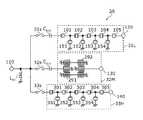
도 1a는 실시 형태 1에 관한 멀티플렉서(1)의 회로 구성도이다. 도 1a에 도시한 바와 같이, 멀티플렉서(1)는 저주파측 필터(11L)와, 고주파측 필터(12H)와, 콘덴서 CB1과, 인덕터 LP1과, 공통 단자(110)와, 입출력 단자(120 및 130)를 구비한다. 멀티플렉서(1)는 공통 단자(110)에 접속된 저주파측 필터(11L) 및 고주파측 필터(12H)를 구비하는 복합 탄성파 필터 장치이다.1A is a circuit configuration diagram of the
공통 단자(110)는, 예를 들어 안테나 소자에 접속 가능하고, 입출력 단자(120 및 130)는 증폭 회로를 통해 고주파 신호 처리 회로에 접속 가능하다.The
저주파측 필터(11L)는, 공통 단자(110)와 입출력 단자(120)(제1 입출력 단자) 사이에 배치되며, 제1 통과 대역(중심 주파수 f011L)을 갖는 제1 필터이다. 저주파측 필터(11L)는, 공통 단자(110)와 입출력 단자(120)를 연결하는 직렬 암에 접속된 직렬 암 공진자(101, 102, 103, 104 및 105)와, 상기 직렬 암과 그라운드 단자를 연결하는 병렬 암에 접속된 병렬 암 공진자(151, 152, 153 및 154)에 의해, 래더형의 밴드 패스 필터를 구성하고 있다. 직렬 암 공진자(101 내지 105) 및 병렬 암 공진자(151 내지 154)는, 탄성 표면파(SAW : Surface Acoustic Wave) 공진자이다. 저주파측 필터(11L)의 각 SAW 공진자는, LiTaO3 기판을 사용한 리키파, 또는, LiNbO3 기판을 사용한 러브파를 이용하고 있다.The low-
본 실시 형태에서는, 저주파측 필터(11L)는, LTE(Long Term Evolution) 규격 Band11의 수신용 필터(수신 통과 대역 : 1475.9-1495.9㎒)에 적용되는 예를 나타내고 있다.In the present embodiment, the low-
고주파측 필터(12H)는, 공통 단자(110)와 입출력 단자(130)(제2 입출력 단자) 사이에 배치되며, 제1 통과 대역보다도 주파수가 높은 제2 통과 대역(중심 주파수 f012H(>f011L))을 갖는 제2 필터이다. 고주파측 필터(12H)는, 공통 단자(110)와 입출력 단자(130)를 연결하는 직렬 암에 접속된 직렬 암 공진자(201, 202, 203, 204 및 205)와, 상기 직렬 암과 그라운드 단자를 연결하는 병렬 암에 접속된 병렬 암 공진자(251, 252, 253 및 254)에 의해, 래더형의 밴드 패스 필터를 구성하고 있다. 또한, 직렬 암 공진자(201 내지 205) 및 병렬 암 공진자(251 내지 254) 중, 공통 단자(110)에 가장 가깝게 접속되어 있는 것은 직렬 암 공진자(201)이다.The high-
본 실시 형태에서는, 직렬 암 공진자(201 내지 205) 및 병렬 암 공진자(251 내지 254)는 모두 SAW 공진자로 하고 있지만, 이들 공진자는, 탄성 경계파나 BAW(Bulk Acoustic Wave)를 사용한 탄성파 공진자여도 된다. 또한, 고주파측 필터(12H)는, 래더형 구조가 아니어도 되고, 나아가, LC 공진 회로와 같은 탄성파 공진자를 갖지 않는 구성이어도 된다.In this embodiment, the
본 실시 형태에서는, 고주파측 필터(12H)는, LTE 규격 Band1의 수신용 필터(수신 통과 대역 : 2110-2170㎒)에 적용되는 예를 나타내고 있다.In this embodiment, the high
콘덴서 CB1은, 공통 단자(110)와 직렬 암 공진자(101)를 연결하는 경로(직렬 암)에 직렬로 배치되어 있다. 여기서, 콘덴서 CB1의 제2 통과 대역에 있어서의 Q값은, 저주파측 필터(11L)의 SAW 공진자의 용량 성분의 제2 통과 대역에 있어서의 용량 Q값보다도 높다. 바꾸어 말하면, 콘덴서 CB1은, 저주파측 필터(11L)의 SAW 공진자의 제2 통과 대역에 있어서의 벌크파 방사 손실을 보상하는 기능을 갖는다. 콘덴서 CB1은 실시 형태 1에 관한 멀티플렉서(1)의 주요부 특징이기 때문에, 콘덴서 CB1에 대해서는, 도 2 이후에 있어서 상세하게 설명한다.The capacitor CB1 is arranged in series in a path (serial arm) connecting the
인덕터 LP1은, 공통 단자(110)와 접지 단자 사이에 접속되어 있다. 이에 의해, 안테나 소자와 각 필터의 임피던스 정합을 확보할 수 있다.The inductor LP1 is connected between the
도 1b는 실시 형태 1의 변형예 1에 관한 멀티플렉서(1A)의 회로 구성도이다. 본 변형예에 관한 멀티플렉서(1A)는, 실시 형태 1에 관한 멀티플렉서(1)와 비교하여, 저주파측 필터의 회로 구성만이 구성으로서 상이하다. 이하, 본 변형예에 관한 멀티플렉서(1A)에 대하여, 실시 형태 1에 관한 멀티플렉서(1)와 동일한 구성에 대해서는 설명을 생략하고, 상이한 구성을 중심으로 설명한다.1B is a circuit configuration diagram of the
도 1b에 도시한 바와 같이, 멀티플렉서(1A)는, 저주파측 필터(13L)와, 고주파측 필터(12H)와, 콘덴서 CB2와, 인덕터 LP2와, 공통 단자(110)와, 입출력 단자(120 및 130)를 구비한다. 멀티플렉서(1A)는, 공통 단자(110)에 접속된 저주파측 필터(13L) 및 고주파측 필터(12H)를 구비하는 복합 탄성파 필터 장치이다.As shown in FIG. 1B, the
저주파측 필터(13L)는, 공통 단자(110)와 입출력 단자(120)(제1 입출력 단자) 사이에 배치되며, 제1 통과 대역(중심 주파수 f013L)을 갖는 제1 필터이다. 저주파측 필터(13L)는, 공통 단자(110)와 입출력 단자(120)를 연결하는 직렬 암에 접속된 직렬 암 공진자(111, 112, 113 및 114)와, 상기 직렬 암과 그라운드 단자를 연결하는 병렬 암에 접속된 병렬 암 공진자(161, 162, 163 및 164)에 의해, 래더형의 밴드 패스 필터를 구성하고 있다. 직렬 암 공진자(111 내지 114) 및 병렬 암 공진자(161 내지 164)는 SAW 공진자이다. 저주파측 필터(13L)의 각 SAW 공진자는, LiTaO3 기판을 사용한 리키파, 또는, LiNbO3 기판을 사용한 러브파를 이용하고 있다. 저주파측 필터(13L)는, 실시 형태 1에 관한 저주파측 필터(11L)와 비교하여, 병렬 암 공진자(161)가 공통 단자(110)에 가장 가깝게 배치되어 있는 점, 및, 직렬 암 공진자의 수가 4개인 점이 상이하다.The low-
콘덴서 CB2는, 공통 단자(110)와 병렬 암 공진자(161)를 연결하는 경로(직렬 암)에 직렬로 배치되어 있다. 여기서, 콘덴서 CB2의 제2 통과 대역에 있어서의 Q값은, 저주파측 필터(13L)의 SAW 공진자의 용량 성분의 제2 통과 대역에 있어서의 용량 Q값보다도 높다. 바꾸어 말하면, 콘덴서 CB2는, 저주파측 필터(13L)의 SAW 공진자의 제2 통과 대역에 있어서의 벌크파 방사 손실을 보상하는 기능을 갖는다.The capacitor CB2 is arranged in series in a path (serial arm) connecting the
인덕터 LP2는, 공통 단자(110)와 접지 단자 사이에 접속되어 있다. 이에 의해, 안테나 소자와 각 필터의 임피던스 정합을 확보할 수 있다.The inductor LP2 is connected between the
즉, 본 발명에 관한 멀티플렉서에서는, 콘덴서 CB1 및 CB2의 후단에 배치되는 저주파측 필터의 공통 단자에 최근접하는 공진자는, 직렬 암 공진자 및 병렬 암 공진자 중 어느 것이어도 된다.That is, in the multiplexer according to the present invention, the resonator closest to the common terminal of the low-frequency filter arranged at the rear ends of the capacitors CB1 and CB2 may be either a series arm resonator or a parallel arm resonator.
다음으로, 비교예에 관한 멀티플렉서의 구성을 설명하고, 당해 비교예에 관한 멀티플렉서의 문제점을 설명한다.Next, the configuration of the multiplexer according to the comparative example will be described, and the problems of the multiplexer according to the comparative example will be described.
[1. 2 비교예에 관한 멀티플렉서][One. 2 Multiplexer according to Comparative Example]
도 2는 비교예에 관한 멀티플렉서(600)의 회로 구성도이다. 도 2에 도시한 바와 같이, 비교예에 관한 멀티플렉서(600)는, 저주파측 필터(611L)와, 고주파측 필터(612H)와, 인덕터 LP3과, 공통 단자(110)와, 입출력 단자(120 및 130)를 구비한다. 멀티플렉서(600)는, 공통 단자(110)에 접속된 저주파측 필터(611L) 및 고주파측 필터(612H)를 구비하는 복합 탄성파 필터 장치이다. 본 비교예에 관한 멀티플렉서(600)는, 실시 형태 1에 관한 멀티플렉서(1)와 비교하여, 콘덴서 CB1이 배치되어 있지 않은 점이, 회로 구성으로서 상이하다.2 is a circuit diagram of a
저주파측 필터(611L)는, 공통 단자(110)와 입출력 단자(120) 사이에 배치되며, 제1 통과 대역(중심 주파수 f0611L)을 갖는 필터이다. 저주파측 필터(611L)의 공진자 구성은, 저주파측 필터(11L)와 동일하다.The low-
고주파측 필터(612H)는, 공통 단자(110)와 입출력 단자(130) 사이에 배치되며, 제1 통과 대역보다도 주파수가 높은 제2 통과 대역(중심 주파수 f0612H(>f0611L))을 갖는 필터이다. 고주파측 필터(12H)의 공진자 구성은, 고주파측 필터(12H)와 동일하다.The high-
LiTaO3 기판을 사용한 리키파나, LiNbO3 기판을 사용한 러브파를 이용하는 SAW 공진자에서는, 반공진점의 고주파측에 벌크파에 의한 손실이 발생한다.In a Ricky wave using a LiTaO3 substrate or a SAW resonator using a love wave using a LiNbO3 substrate, loss due to a bulk wave occurs on the high frequency side of the anti-resonance point.
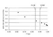
도 3a는 저주파측 필터(611L)의 광역 통과 특성을 나타내는 그래프이다. 또한, 도 3b는 저주파측 필터(611L)의 광역 반사 특성을 나타내는 그래프이다. 또한, 도 3c는 저주파측 필터(611L)의 반사 특성을 나타내는 폴라 차트이다. 상기 SAW 공진자를 포함한 저주파측 필터(611L)에서는, 중심 주파수 f0611L의 고주파측의 감쇠 대역에 있어서 상기 벌크파 방사가 발생하여, 도 3b에 도시한 바와 같이, 당해 감쇠 대역(도 3b의 마커 5 이상의 주파수)에 있어서 공통 단자(110)측으로부터 저주파측 필터(611L)를 본 경우의 리턴 로스가 증가된다. 이 벌크파에 의한 손실은, 도 3a에 도시한 바와 같이, 저주파측 필터(611L)의 감쇠량에는 거의 영향을 미치지 않는다. 그러나, 도 3c에 도시한 바와 같이, 상기 감쇠 대역(도 3c의 마커 5 이상의 주파수)에 있어서 반사 계수(|Γ|)를 저하시킨다(|Γ|=0.84).3A is a graph showing the wide-pass characteristics of the low-
SAW 공진자를 포함한 저주파측 필터(611L)는, 상기 감쇠 대역에서는 용량성의 특성을 갖고 콘덴서로서 기능하기 때문에, 상기 벌크파가 발생한 주파수대(도 3b의 마커 5 이상의 주파수)에서는, Q값이 낮은 콘덴서로서 기능한다. 이 때문에, 저주파측 필터(611L) 및 고주파측 필터(612H)가 공통 단자(110)에 접속된 구성을 갖는 멀티플렉서(600)의 경우, 통과 대역이 낮은 저주파측 필터(611L)의 벌크파 손실에 의해, 당해 벌크파 손실이 발생하는 주파수를 통과 대역으로 하는 고주파측 필터(612H)의 필터 특성이 영향을 받는다. 도 2의 우측에, 이때의 고주파측 필터(612H)의 등가 회로를 도시한다. 이 등가 회로에서는, 공통 단자(110)와 고주파측 필터(612H)의 직렬 암 공진자(201) 사이에, 저주파측 필터(611L)의 벌크파 방사에 기인한 Q값이 낮은 등가 용량 성분 CLow-Q가 존재하게 된다. 이에 의해, 고주파측 필터(612H)의 통과 대역 내의 삽입 손실이 커져 버린다. 즉, 공통 단자로 복수의 필터를 연결한 구성을 갖는 멀티플렉서에 있어서, 저주파측 필터의 벌크파 손실에 의해, 고주파측 필터의 통과 대역 내 손실이 커진다는 문제가 발생한다.Since the low-
[1. 3 실시 형태 및 비교예에 관한 멀티플렉서의 특성 비교][One. Comparison of characteristics of multiplexer according to
비교예에 관한 멀티플렉서(600)의 문제를 해결하기 위해, 본 실시 형태에 관한 멀티플렉서(1)에서는, 전술한 바와 같이, 공통 단자(110)와 직렬 암 공진자(101)를 연결하는 경로(직렬 암)에, 콘덴서 CB1이 직렬로 배치되어 있다. 콘덴서 CB1은, 저주파측 필터(11L)의 SAW 공진자의 제2 통과 대역에 있어서의 벌크파 방사 손실을 보상하는 기능을 갖는다. 보다 구체적으로는, 콘덴서 CB1의 제2 통과 대역에 있어서의 Q값은, 저주파측 필터(11L)의 SAW 공진자의 용량 성분의 제2 통과 대역에 있어서의 용량 Q값보다도 높다.In order to solve the problem of the
도 4a는 실시 형태 1에 관한 고주파측 필터(12H)의 광역 통과 특성을 나타내는 그래프이다. 또한, 도 4b는 비교예에 관한 고주파측 필터(612H)의 광역 통과 특성을 나타내는 그래프이다.4A is a graph showing the wide-pass characteristics of the high-
도 4b에 도시한 바와 같이, 비교예에 관한 멀티플렉서(600)의 경우, 저주파측 필터(611L)를 구성하는 각 SAW 공진자의 벌크파 방사에 의해, 고주파측 필터(612H)의 공통 단자(110)-입출력 단자(130) 간의 통과 특성에 있어서, 통과 대역 내(2110-2170㎒)에 있어서의 최대 삽입 손실은 2.638㏈(2170㎒)로 되어 있다.As shown in Fig. 4B, in the case of the
이에 반해, 도 4a에 도시한 바와 같이, 실시 형태 1에 관한 멀티플렉서(1)의 경우, 저주파측 필터(11L)를 구성하는 각 SAW 공진자의 벌크파 방사에 대하여, 콘덴서 CB1이 부가되어 있음으로써, 고주파측 필터(12H)의 공통 단자(110)-입출력 단자(130) 간의 통과 특성에 있어서, 통과 대역 내(2110-2170㎒)에 있어서의 최대 삽입 손실은, 2.119㏈(2170㎒)로 되어 있어, 약 0.5㏈ 개선되어 있다.On the other hand, as shown in Fig. 4A, in the case of the
즉, 실시 형태 1에 관한 멀티플렉서(1)에 따르면, 저주파측 필터(11L) 및 고주파측 필터(12H)의 전단에 분파/합파기나 위상 조정 회로 등을 배치하지 않더라도 고주파 신호의 전파 손실을 저감할 수 있어, 소형화 및 저비용화가 가능해진다.That is, according to the
여기서, 도 2의 우측에 도시된 등가 회로와 같이 고주파측 필터의 전단에 저주파측 필터에 기인하는 용량이 등가적으로 부가되는 경우의, 당해 등가 용량 성분의 Q값, 고주파측 필터의 통과 대역에 있어서의 저주파측 필터의 반사 계수(|Γ|), 및, 고주파측 필터의 통과 대역에 있어서의 삽입 손실의 관계를, 도 5a 내지 도 5d를 사용하여 설명한다.Here, as in the equivalent circuit shown on the right side of Fig. 2, when the capacity attributable to the low-frequency filter is equivalently added to the front end of the high-frequency filter, the Q value of the equivalent capacity component and the pass band of the high-frequency filter The relationship between the reflection coefficient (|Γ|) of the low-frequency side filter and the insertion loss in the pass band of the high-frequency side filter will be described using FIGS. 5A to 5D.
도 5a는 고주파측 필터 전단의 등가 용량 성분의 Q값, 저주파측 필터의 반사 계수, 및 고주파측 필터의 삽입 손실의 관계를 도시하는 도면이다. 도 5a에 도시한 바와 같이, 저주파측 필터의 반사 계수(|Γ|)가 작아질수록, 고주파측 필터 전단의 등가 용량 성분의 Q값이 작아져, 고주파측 필터의 삽입 손실이 악화되어 있는 것을 알 수 있다.Fig. 5A is a diagram showing the relationship between the Q value of the equivalent capacitance component before the high-frequency filter, the reflection coefficient of the low-frequency filter, and the insertion loss of the high-frequency filter. As shown in Fig. 5A, the smaller the reflection coefficient (|Γ|) of the low-frequency side filter, the smaller the Q value of the equivalent capacity component before the high-frequency side filter, and that the insertion loss of the high-frequency side filter deteriorates. Able to know.
도 5b는 고주파측 필터 전단의 등가 용량 성분의 Q값과 고주파측 필터의 삽입 손실의 관계를 나타내는 그래프이다. 또한, 도 5c는 저주파측 필터의 반사 계수와 고주파측 필터의 삽입 손실의 관계를 나타내는 그래프이다. 또한, 도 5d는 고주파측 필터 전단의 등가 용량 성분의 Q값과 저주파측 필터의 반사 계수의 관계를 나타내는 그래프이다. 도 5b 내지 도 5d로부터, 비교예에 관한 멀티플렉서(600)의 경우, 고주파측 필터(612H) 전단의 등가 용량 성분의 Q값은 5이며, 실시 형태 1에 관한 멀티플렉서(1)의 경우, 고주파측 필터(12H) 전단의 등가 용량 성분의 Q값은 10인 것을 알 수 있다. 또한, 비교예에 관한 멀티플렉서(600)의 경우, 저주파측 필터(611L)의 반사 계수(|Γ|)는 0.84이며, 실시 형태 1에 관한 멀티플렉서(1)의 경우, 저주파측 필터(11L)의 반사 계수(|Γ|)는 0.9 이상인 것을 알 수 있다.5B is a graph showing the relationship between the Q value of the equivalent capacitance component in front of the high-frequency filter and the insertion loss of the high-frequency filter. 5C is a graph showing the relationship between the reflection coefficient of the low-frequency filter and the insertion loss of the high-frequency filter. 5D is a graph showing the relationship between the Q value of the equivalent capacitance component at the front end of the high-frequency filter and the reflection coefficient of the low-frequency filter. 5B to 5D, in the case of the
즉, 비교예에 관한 멀티플렉서(600)의 경우, 고주파측 필터(612H)의 통과 대역에 있어서의 저주파측 필터(611L)의 반사 계수(|Γ|)는 0.84이다. 이에 반해, 실시 형태 1에 관한 멀티플렉서(1)의 경우, 저주파측 필터(11L)의 전단에 콘덴서 CB1이 직렬 배치됨으로써, 고주파측 필터(12H)의 통과 대역에 있어서의 저주파측 필터(11L)의 반사 계수(|Γ|)는 0.9 이상으로 상승하고, 또한, 고주파측 필터(12H)의 전단의 등가 용량 성분의 Q값이, 5로부터 10으로 증가된다. 이에 의해, 실시 형태 1에 관한 고주파측 필터(12H)의 삽입 손실이, 2.638㏈로부터 2.119㏈로 개선된다. 또한, 본 실시 형태에서는, 고주파측 필터(12H)의 등가 용량 성분의 Q값을, 5로부터 10으로 증가시키기 위해, 콘덴서 CB1의 고주파측 필터(12H)의 통과 대역에 있어서의 Q값을, 30 내지 40 정도로 설정하였다.That is, in the case of the
[1. 4 콘덴서의 구성][One. 4 Condenser configuration]
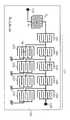
다음으로, 실시 형태 1에 관한 콘덴서 CB1 및 CB2의 구성에 대하여 설명한다.Next, the configuration of the capacitors CB1 and CB2 according to the first embodiment will be described.
도 6a는 실시 형태 1에 관한 저주파측 필터(11L) 및 콘덴서 CB1의 전극 레이아웃의 제1 예를 도시하는 평면도이다. 도 6a에 도시한 바와 같이, 멀티플렉서(1)가 갖는 저주파측 필터(11L) 및 콘덴서 CB1은, 기판(100) 상에 형성되어 있다. 저주파측 필터(11L)의 직렬 암 공진자(101 내지 105) 및 병렬 암 공진자(151 내지 154)를 구성하는 IDT 전극은, 이용하는 탄성파의 전파 방향이 일치하도록 기판(100) 상에 형성되어 있다.6A is a plan view showing a first example of the electrode layout of the low-
또한, 콘덴서 CB1은, 서로 대향하는 빗형 전극에 의해 기판(100) 상에 형성되어 있다.In addition, the capacitor CB1 is formed on the
또한, 기판(100)은 적어도 일부에 압전성을 갖는 기판이며, 예를 들어 압전 기판이며, 또한, 압전 박막과 지지 기판을 포함하고 있어도 된다.Further, the
여기서, 콘덴서 CB1의 빗형 전극을 구성하는 복수의 전극 핑거의 피치 Pc는, 직렬 암 공진자(101 내지 105)의 IDT 전극을 구성하는 복수의 전극 핑거의 피치 λs 및 병렬 암 공진자(151 내지 154)의 IDT 전극을 구성하는 복수의 전극 핑거의 피치 λp보다도 작다.Here, the pitch Pc of the plurality of electrode fingers constituting the comb electrode of the capacitor CB1 is the pitch λs of the plurality of electrode fingers constituting the IDT electrodes of the
본 실시 형태에 관한 멀티플렉서(1)에 있어서, 저주파측 필터(11L)의 직렬 암 공진자(101 내지 105)의 전극 핑거의 피치 λs는, 예를 들어 2.350 내지 2.370㎛이며, 병렬 암 공진자(151 내지 154)의 전극 핑거의 피치 λp는, 예를 들어 2.410 내지 2.430㎛이다. 이에 반해, 콘덴서 CB1의 전극 핑거의 피치 Pc는, 예를 들어 1.8㎛로 되어 있다.In the
기판(100) 상의 콘덴서 CB1에 있어서도, SAW 공진자와 마찬가지로, 콘덴서 CB1의 Q값은 벌크파에 영향을 받는다. 상기 구성에 따르면, 저주파측 필터(11L)에 의한 벌크파 방사의 주파수보다도, 콘덴서 CB1에 의한 벌크파 방사의 주파수가 고주파측으로 시프트하므로, 제2 통과 대역에 있어서의 콘덴서 CB1의 Q값을, 저주파측 필터(11L)의 SAW 공진자의 제2 통과 대역에 있어서의 용량 Q값보다도 높게 설정할 수 있다. 이 때문에, 저주파측 필터(11L)의 공통 단자(110)측에 있어서, 제2 통과 대역에 있어서의 용량 Q값을 올릴 수 있다. 이에 의해, 저주파측 필터(11L)의 제2 통과 대역에 있어서의 반사 계수(|Γ|)를 올릴(리턴 로스를 저감할) 수 있어, 고주파측 필터(12H)의 제2 통과 대역에 있어서의 삽입 손실을 개선하는 것이 가능해진다.In the capacitor CB1 on the
또한, 기판(100) 상에 형성되는 콘덴서 CB1의 빗형 전극을 구성하는 복수의 전극 핑거의 방향은, 저주파측 필터(11L)의 각 공진자를 구성하는 복수의 전극 핑거의 방향과 직교(교차)하고 있는 것이 바람직하다. 이에 의해, 콘덴서 CB1은, 저주파측 필터(11L)의 탄성파와 간섭하는 것이 억제되어, 용량 소자로서만 기능하는 것이 가능해진다.In addition, the direction of the plurality of electrode fingers constituting the comb-shaped electrode of the capacitor CB1 formed on the
또한, 고주파측 필터(12H)가 SAW 공진자를 포함하고 있는 경우에는, 콘덴서 CB1의 빗형 전극을 구성하는 복수의 전극 핑거의 피치는, 고주파측 필터(12H)를 구성하는 SAW 공진자의 전극 핑거의 피치보다 작은 쪽이 더욱 바람직하다.In addition, when the high-
본 실시 형태에 관한 멀티플렉서(1)에 있어서, 고주파측 필터(12H)의 직렬 암 공진자(201 내지 205)의 전극 핑거의 피치 λs는, 예를 들어 1.980 내지 2.000㎛이며, 병렬 암 공진자(251 내지 254)의 전극 핑거의 피치 λp는, 예를 들어 2.070 내지 2.090㎛이다. 압전 기판 상의 콘덴서에 있어서도, 공진자와 마찬가지로 벌크파에 의한 Q 악화가 있기 때문에, 고주파수측의 피치보다 좁게 설계하는 것이 좋다. 이 구성에 따르면, 고주파측 필터(12H)에 의한 벌크파 방사의 주파수보다도, 콘덴서 CB1에 의한 벌크파 방사의 주파수가 고주파측으로 시프트하므로, 제2 통과 대역에 있어서의 콘덴서 CB1의 Q값을, 고주파측 필터(12H)의 SAW 공진자의 제2 통과 대역에 있어서의 용량 Q값보다도 높게 설정할 수 있다. 이 때문에, 저주파측 필터(11L)의 공통 단자(110)측에 있어서, 제2 통과 대역에 있어서의 용량 Q값을 더 올릴 수 있다. 이에 의해, 저주파측 필터(11L)의 제2 통과 대역에 있어서의 반사 계수(|Γ|)를 올릴(리턴 로스를 저감할) 수 있어, 고주파측 필터(12H)의 제2 통과 대역에 있어서의 삽입 손실을 개선하는 것이 가능해진다.In the
또한, 콘덴서 CB1은, 상기 기판(100) 상이 아니라, 저주파측 필터(11L) 및 고주파측 필터(12H)를 실장함과 함께, 저주파측 필터(11L)와 고주파측 필터(12H)를 접속하는 배선을 구성하는 다층 기판 내의 복수층으로 형성되어 있어도 된다.In addition, the capacitor CB1 is mounted on the low
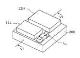
도 6b는 실시 형태 1에 관한 멀티플렉서의 외관 사시도의 일례이다. 또한, 도 6c는 실시 형태 1에 관한 저주파측 필터 및 콘덴서의 전극 레이아웃의 제2 예를 도시하는 단면도이다. 구체적으로는, 도 6c는 도 6b의 VI-VI선에 있어서의 단면도이다.6B is an example of the external perspective view of the multiplexer which concerns on
이들 도면에 도시된 바와 같이, 실시 형태 1에 관한 멀티플렉서(1)에서는, 실장 기판(200) 상에, 저주파측 필터(11L), 고주파측 필터(12H) 및 인덕터 LP1이 실장되어 있다.As shown in these figures, in the
실장 기판(200)은 콘덴서 CB1 및 저주파측 필터와 고주파측 필터를 접속하는 배선을 내장하는, 예를 들어 LTCC(Low Temperature Co-fired Ceramics) 기판이다.The mounting
도 6c에 도시한 바와 같이, 콘덴서 CB1은, 세라믹 다층 기판인 실장 기판(200)에, 복수층에 걸쳐 형성되어 있다. 또한, 실장 기판(200)은 HTCC(High Temperature Co-fired Ceramics) 기판이나 PCB를 포함하는 다층 기판의 복수층에 걸쳐 형성되어 있어도 된다. 또한, 다층 기판 상에 칩 콘덴서(MLCC : Multi Layer Ceramic Capacitor)를 탑재하여 형성해도 된다.As shown in Fig. 6C, the capacitor CB1 is formed over a plurality of layers on the mounting
이에 의해, 저주파측 필터(11L)의 각 SAW 공진자의 IDT 전극이 기판(100)의 일 표면 상에 형성되어 있는 것에 반해, 콘덴서 CB1은, 유전체층을 사이에 두고 서로 대향하는 복수의 평면 전극에 의해 형성되어 있으므로, 제2 통과 대역에 있어서의 콘덴서의 Q값을, 저주파측 필터(11L)의 각 SAW 공진자의 제2 통과 대역에 있어서의 용량 Q값보다도 높게 설정할 수 있다. 이 때문에, 저주파측 필터(11L)의 공통 단자(110)측에 있어서, 제2 통과 대역에 있어서의 용량 Q값을 올릴 수 있다. 이에 의해, 저주파측 필터(11L)의 제2 통과 대역에 있어서의 반사 계수(|Γ|)를 올릴(리턴 로스를 저감할) 수 있어, 고주파측 필터(12H)의 제2 통과 대역에 있어서의 삽입 손실을 개선하는 것이 가능해진다.Thereby, while the IDT electrode of each SAW resonator of the low-
[1. 5 저주파측 필터 및 고주파측 필터의 변형예][One. 5 Modifications of low-frequency and high-frequency filters]
도 7a는 실시 형태 1의 변형예 2에 관한 멀티플렉서(1B)의 회로 구성도이다. 도 7a에 도시한 바와 같이, 본 발명에 관한 멀티플렉서를 구성하는 저주파측 필터 및 고주파측 필터는, 종결합형 SAW 공진부를 포함하는 구성이어도 된다. 본 변형예에 관한 멀티플렉서(1B)는, 저주파측 필터(15L)와, 고주파측 필터(16H)와, 콘덴서 CB3과, 인덕터 LP4와, 공통 단자(110)와, 입출력 단자(120 및 130)를 구비한다. 멀티플렉서(1B)는, 공통 단자(110)에 접속된 저주파측 필터(15L) 및 고주파측 필터(16H)를 구비하는 복합 탄성파 필터 장치이다.7A is a circuit configuration diagram of the
저주파측 필터(15L)는, 공통 단자(110)와 입출력 단자(120)(제1 입출력 단자) 사이에 배치되며, 제1 통과 대역(중심 주파수 f015L)을 갖는 제1 필터이다. 저주파측 필터(15L)는, 공통 단자(110)와 입출력 단자(120)를 연결하는 직렬 암에 접속된 직렬 암 공진자(121 및 122)와, 상기 직렬 암과 그라운드 단자를 연결하는 병렬 암에 접속된 병렬 암 공진자(171)와, 직렬 암 공진자(121 및 122)에 접속된 종결합형 SAW 공진부(125)에 의해, 밴드 패스 필터를 구성하고 있다. 직렬 암 공진자(121 및 122), 병렬 암 공진자(171), 및 종결합형 SAW 공진부(125)를 구성하는 5개의 공진자는 SAW 공진자이다. 저주파측 필터(15L)의 각 SAW 공진자는, LiTaO3 기판을 사용한 리키파, 또는, LiNbO3 기판을 사용한 러브파를 이용하고 있다.The low-
고주파측 필터(16H)는, 공통 단자(110)와 입출력 단자(130)(제2 입출력 단자) 사이에 배치되며, 제1 통과 대역보다도 주파수가 높은 제2 통과 대역(중심 주파수 f016H(>f015L))을 갖는 제2 필터이다. 고주파측 필터(16H)는, 공통 단자(110)와 입출력 단자(130)를 연결하는 직렬 암에 접속된 직렬 암 공진자(211, 212 및 213)와, 상기 직렬 암과 그라운드 단자를 연결하는 병렬 암에 접속된 병렬 암 공진자(261)와, 직렬 암 공진자(212 및 213)에 접속된 종결합형 SAW 공진부(215)에 의해, 밴드 패스 필터를 구성하고 있다. 또한, 상기 각 공진자 중, 공통 단자(110)에 가장 가깝게 접속되어 있는 것은 직렬 암 공진자(211)이다. 직렬 암 공진자(211, 212 및 213), 병렬 암 공진자(261), 및 종결합형 SAW 공진부(215)를 구성하는 5개의 공진자는, SAW 공진자이다. 또한, 상기 각 공진자는, 탄성 경계파나 BAW를 사용한 탄성파 공진자여도 된다. 또한, 고주파측 필터(16H)는, LC 공진 회로와 같은 탄성파 공진자를 갖지 않는 구성이어도 된다.The high-
콘덴서 CB3은, 공통 단자(110)와 병렬 암 공진자(171)를 연결하는 경로(직렬 암)에 직렬로 배치되어 있다. 여기서, 콘덴서 CB3의 제2 통과 대역에 있어서의 Q값은, 저주파측 필터(15L)의 SAW 공진자의 용량 성분의 제2 통과 대역에 있어서의 용량 Q값보다도 높다. 바꾸어 말하면, 콘덴서 CB3은, 저주파측 필터(15L)의 SAW 공진자의 제2 통과 대역에 있어서의 벌크파 방사 손실을 보상하는 기능을 갖는다.The capacitor CB3 is arranged in series in a path (serial arm) connecting the
인덕터 LP4는, 공통 단자(110)와 접지 단자 사이에 접속되어 있다. 이에 의해, 안테나 소자와 각 필터의 임피던스 정합을 확보할 수 있다.The inductor LP4 is connected between the
상기 구성에 의해, 저주파측 필터(15L)의 제2 통과 대역에 있어서의 반사 계수(|Γ|)를 올릴(리턴 로스를 저감할) 수 있으므로, 저주파측 필터(15L)와 함께 공통 단자(110)에 접속된 고주파측 필터(16H)의 제2 통과 대역에 있어서의 삽입 손실을 개선하는 것이 가능해진다. 따라서, 각각의 필터의 전단에 분파/합파기나 위상 조정 회로 등을 배치하지 않더라도 고주파 신호의 전파 손실을 저감할 수 있어, 소형화 및 저비용화가 가능해진다.With the above configuration, since the reflection coefficient (|Γ|) in the second pass band of the low-
또한, 도 7b는 실시 형태 1의 변형예 3에 관한 멀티플렉서(1C)의 회로 구성도이다. 도 7b에 도시한 바와 같이, 저주파측 필터(17L)가 래더형의 SAW 필터이며, 고주파측 필터(18H)가, 종결합 SAW 공진부(225)를 포함하는 SAW 필터여도 된다.7B is a circuit configuration diagram of the
본 변형예에 관한 멀티플렉서(1C)는, 저주파측 필터(17L)와, 고주파측 필터(18H)와, 콘덴서 CB4와, 인덕터 LP5와, 공통 단자(110)와, 입출력 단자(120 및 130)를 구비한다.The
저주파측 필터(17L)는, 제1 통과 대역(중심 주파수 f017L)을 갖는 제1 필터이다. 저주파측 필터(17L)는, 공통 단자(110)와 입출력 단자(120)를 연결하는 직렬 암에 접속된 직렬 암 공진자(131, 132, 133 및 134)와, 상기 직렬 암과 그라운드 단자를 연결하는 병렬 암에 접속된 병렬 암 공진자(181, 182, 183 및 184)에 의해, 래더형의 밴드 패스 필터를 구성하고 있다.The low-
고주파측 필터(18H)는, 변형예 2에 관한 고주파측 필터(16H)와 마찬가지의 구성이며, 제1 통과 대역보다도 주파수가 높은 제2 통과 대역(중심 주파수 f018H(>f017L))을 갖는 제2 필터이다. 고주파측 필터(18H)는, 공통 단자(110)와 입출력 단자(130)를 연결하는 직렬 암에 접속된 직렬 암 공진자(221, 222 및 223)와, 상기 직렬 암과 그라운드 단자를 연결하는 병렬 암에 접속된 병렬 암 공진자(271)와, 직렬 암 공진자(222 및 223)에 접속된 종결합형 SAW 공진부(225)에 의해, 밴드 패스 필터를 구성하고 있다. 또한, 상기 각 공진자 중, 공통 단자(110)에 가장 가깝게 접속되어 있는 것은 직렬 암 공진자(221)이다.The high-
상기 구성에 의해, 저주파측 필터(17L)의 제2 통과 대역에 있어서의 반사 계수(|Γ|)를 올릴(리턴 로스를 저감할) 수 있으므로, 저주파측 필터(17L)와 함께 공통 단자(110)에 접속된 고주파측 필터(18H)의 제2 통과 대역에 있어서의 삽입 손실을 개선하는 것이 가능해진다. 따라서, 각각의 필터의 전단에 분파/합파기나 위상 조정 회로 등을 배치하지 않더라도 고주파 신호의 전파 손실을 저감할 수 있어, 소형화 및 저비용화가 가능해진다.With the above configuration, since the reflection coefficient (|Γ|) in the second pass band of the low-
(실시 형태 2)(Embodiment 2)
실시 형태 1에서는, 저주파측 필터 및 고주파측 필터를 공통 단자에 접속한 구성을 갖는 2분파/합파용의 멀티플렉서를 들었지만, 본 실시 형태에서는, 서로 통과 대역이 상이한 3개의 필터를 공통 단자에 접속한 구성을 갖는 3분파/합파용의 멀티플렉서에 대하여 설명한다.In the first embodiment, a multiplexer for two-wave/harmonics having a configuration in which a low-frequency side filter and a high-frequency side filter are connected to a common terminal is heard, but in this embodiment, three filters having different pass bands are connected to a common terminal. A multiplexer for a three-wave/hap wave having a configuration will be described.
[2. 1 멀티플렉서의 회로 구성][2. 1 Circuit configuration of multiplexer]
도 8a는 실시 형태 2에 관한 멀티플렉서(2)의 회로 블록도이다. 도 8a에 도시한 바와 같이, 멀티플렉서(2)는 로우 밴드용 필터(21L)와, 미들 밴드용 필터(22M)와, 하이 밴드용 필터(23H)와, 콘덴서 CBL 및 CBM과, 공통 단자(110)와, 입출력 단자(120, 130 및 140)를 구비한다. 멀티플렉서(2)는 공통 단자(110)에 접속된 로우 밴드용 필터(21L), 미들 밴드용 필터(22M) 및 하이 밴드용 필터(23H)를 구비하는 복합 탄성파 필터 장치이다.8A is a circuit block diagram of the
공통 단자(110)는, 예를 들어 안테나 소자에 접속 가능하고, 입출력 단자(120, 130 및 140)는 증폭 회로를 통해 고주파 신호 처리 회로에 접속 가능하다.The
로우 밴드용 필터(21L)는, 공통 단자(110)와 입출력 단자(120)(제1 입출력 단자) 사이에 배치되며, 제1 통과 대역(중심 주파수 f021L)을 갖는 제1 필터이다. 로우 밴드용 필터(21L)는 1 이상의 SAW 공진자를 포함하고 있다.The low-
미들 밴드용 필터(22M)는, 공통 단자(110)와 입출력 단자(130)(제1 입출력 단자) 사이에 배치되며, 제1 통과 대역보다도 주파수가 높은 제3 통과 대역(중심 주파수 f022M)을 갖는 제3 필터이다. 미들 밴드용 필터(22M)는, 1 이상의 SAW 공진자를 포함하고 있다.The
하이 밴드용 필터(23H)는, 공통 단자(110)와 입출력 단자(140)(제2 입출력 단자) 사이에 배치되며, 제3 통과 대역보다도 주파수가 높은 제2 통과 대역(중심 주파수 f023H(>f022M))을 갖는 제2 필터이다. 하이 밴드용 필터(23H)는, 1 이상의 SAW 공진자를 포함하고 있다. 또한, 본 실시 형태에서는, 하이 밴드용 필터(23H)를 구성하는 각 공진자는, 모두 SAW 공진자로 하고 있지만, 이들 공진자는, 탄성 경계파나 BAW를 사용한 탄성파 공진자여도 된다. 또한, 하이 밴드용 필터(23H)는, LC 공진 회로와 동일한 탄성파 공진자를 갖지 않는 구성이어도 된다.The high-
콘덴서 CBL은, 공통 단자(110)와 로우 밴드용 필터(21L)를 연결하는 경로(직렬 암)에 직렬로 배치되어 있다. 여기서, 콘덴서 CBL의 제2 통과 대역 및 제3 통과 대역에 있어서의 Q값은, 로우 밴드용 필터(21L)의 SAW 공진자의 용량 성분의 제2 통과 대역 및 제3 통과 대역에 있어서의 용량 Q값보다도 높다. 바꾸어 말하면, 콘덴서 CBL은, 로우 밴드용 필터(21L)의 SAW 공진자의 제2 통과 대역 및 제3 통과 대역에 있어서의 벌크파 방사 손실을 보상하는 기능을 갖는다.The capacitor CBL is arranged in series in a path (serial arm) connecting the
콘덴서 CBM은, 공통 단자(110)와 미들 밴드용 필터(22M)를 연결하는 경로(직렬 암)에 직렬로 배치되어 있다. 여기서, 콘덴서 CBM의 제2 통과 대역에 있어서의 Q값은, 미들 밴드용 필터(22M)의 SAW 공진자의 용량 성분의 제2 통과 대역에 있어서의 용량 Q값보다도 높다. 바꾸어 말하면, 콘덴서 CBM은, 미들 밴드용 필터(22M)의 SAW 공진자의 제2 통과 대역에 있어서의 벌크파 방사 손실을 보상하는 기능을 갖는다.The capacitor CBM is arranged in series in a path (serial arm) connecting the
도 8b는 실시 형태 2에 관한 멀티플렉서(2A)의 회로 구성도이다. 도 8b에 도시된 멀티플렉서(2A)는, 멀티플렉서(2)의 구체적 회로 구성을 도시한 것이다. 도 8b에 도시한 바와 같이, 멀티플렉서(2A)는, 로우 밴드용 필터(21L)와, 미들 밴드용 필터(22M)와, 하이 밴드용 필터(23H)와, 콘덴서 CB5 및 CB6과, 인덕터 LP6과, 공통 단자(110)와, 입출력 단자(120, 130 및 140)를 구비한다.8B is a circuit configuration diagram of the
로우 밴드용 필터(21L)는, 실시 형태 1에 관한 저주파측 필터(11L)와 동일한 구성을 갖는다. 로우 밴드용 필터(21L)의 각 SAW 공진자는, LiTaO3 기판을 사용한 리키파, 또는, LiNbO3 기판을 사용한 러브파를 이용하고 있다.The low-
미들 밴드용 필터(22M)는, 로우 밴드용 필터(21L)와 마찬가지의 공진자 구성을 갖고, 공통 단자(110)와 입출력 단자(130)를 연결하는 직렬 암에 접속된 직렬 암 공진자(201 내지 205)와, 상기 직렬 암과 그라운드 단자를 연결하는 병렬 암에 접속된 병렬 암 공진자(251 내지 254)에 의해, 래더형의 밴드 패스 필터를 구성하고 있다. 미들 밴드용 필터(22M)의 각 SAW 공진자는, LiTaO3 기판을 사용한 리키파, 또는, LiNbO3 기판을 사용한 러브파를 이용하고 있다.The
하이 밴드용 필터(23H)는, 실시 형태 1에 관한 고주파측 필터(12H)와 동일한 구성을 갖고, 공통 단자(110)와 입출력 단자(130)를 연결하는 직렬 암에 접속된 직렬 암 공진자(301 내지 305)와, 상기 직렬 암과 그라운드 단자를 연결하는 병렬 암에 접속된 병렬 암 공진자(351 내지 354)에 의해, 래더형의 밴드 패스 필터를 구성하고 있다. 또한, 직렬 암 공진자(301 내지 305) 및 병렬 암 공진자(351 내지 354) 중, 공통 단자(110)에 가장 가깝게 접속되어 있는 것은 직렬 암 공진자(301)이다.The high-
콘덴서 CB5는, 멀티플렉서(2)에 있어서의 콘덴서 CBL이며, 콘덴서 CB6은, 멀티플렉서(2)에 있어서의 콘덴서 CBM이다.The capacitor CB5 is the capacitor CBL in the
인덕터 LP6은, 공통 단자(110)와 접지 단자 사이에 접속되어 있다. 이에 의해, 안테나 소자와 각 필터의 임피던스 정합을 확보할 수 있다.The inductor LP6 is connected between the
콘덴서 CB5의 배치에 의해, 로우 밴드용 필터(21L)의 제2 통과 대역 및 제3 통과 대역에 있어서의 반사 계수(|Γ|)를 올릴(리턴 로스를 저감할) 수 있으므로, 로우 밴드용 필터(21L)와 함께 공통 단자(110)에 접속된 하이 밴드용 필터(23H)의 제2 통과 대역 및 미들 밴드용 필터(22M)의 제3 통과 대역에 있어서의 삽입 손실을 개선하는 것이 가능해진다.By arranging the condenser CB5 , the reflection coefficients (|Γ|) in the second pass band and the third pass band of the
또한, 콘덴서 CB6의 배치에 의해, 미들 밴드용 필터(22M)의 제2 통과 대역에 있어서의 반사 계수(|Γ|)를 올릴(리턴 로스를 저감할) 수 있으므로, 미들 밴드용 필터(22M)와 함께 공통 단자(110)에 접속된 하이 밴드용 필터(23H)의 제2 통과 대역에 있어서의 삽입 손실을 개선하는 것이 가능해진다.Further, by arranging the capacitor CB6 , since the reflection coefficient (|Γ|) in the second pass band of the
상기 구성에 따르면, 각각의 필터의 전단에 3분파/합파기나 위상 조정 회로 등을 배치하지 않더라도 고주파 신호의 전파 손실을 저감할 수 있어, 소형화 및 저비용화가 가능해진다.According to the above configuration, even if a three-wave/combiner or a phase adjustment circuit is not disposed in front of each filter, propagation loss of a high-frequency signal can be reduced, and miniaturization and cost reduction are possible.
도 8c는 실시 형태 2의 변형예 1에 관한 멀티플렉서(2B)의 회로 구성도이다. 도 8c에 도시된 멀티플렉서(2B)는, 실시 형태 2에 관한 멀티플렉서(2A)와 비교하여, 로우 밴드용 필터(21L) 및 미들 밴드용 필터(22M)의 회로 구성만이 상이하다. 이하, 본 변형예에 관한 멀티플렉서(2B)에 대하여, 실시 형태 2에 관한 멀티플렉서(2A)와 상이한 구성만 설명한다.8C is a circuit configuration diagram of the
본 변형예에 관한 로우 밴드용 필터(21L)는, 실시 형태 1의 변형예 1에 관한 저주파측 필터(13L)와 동일한 구성을 갖는다.The low-
본 변형예에 관한 미들 밴드용 필터(22M)는, 본 변형예에 관한 로우 밴드용 필터(21L)와 마찬가지의 공진자 구성을 갖고 있다.The
콘덴서 CB7은, 멀티플렉서(2)에 있어서의 콘덴서 CBL이며, 콘덴서 CB8은, 멀티플렉서(2)에 있어서의 콘덴서 CBM이다.The capacitor CB7 is the capacitor CBL in the
즉, 본 발명에 관한 멀티플렉서에서는, 콘덴서 CBL 및 CBM의 후단에 배치되는 로우 밴드용 필터(21L) 및 미들 밴드용 필터(22M)의 공통 단자에 최근접하는 공진자는, 직렬 암 공진자 및 병렬 암 공진자 중 어느 것이어도 된다.That is, in the multiplexer according to the present invention, the resonators closest to the common terminals of the low-
도 8d는 실시 형태 2의 변형예 2에 관한 멀티플렉서(2C)의 회로 구성도이다. 도 8d에 도시된 멀티플렉서(2C)는, 실시 형태 2에 관한 멀티플렉서(2A)와 비교하여, 로우 밴드용 필터(21L) 및 미들 밴드용 필터(22M)의 구성이 상이하다. 이하, 본 변형예에 관한 멀티플렉서(2C)에 대하여, 실시 형태 2에 관한 멀티플렉서(2A)와 상이한 구성만 설명한다.8D is a circuit configuration diagram of the
본 변형예에 관한 로우 밴드용 필터(21L)는, 실시 형태 2의 변형예 1에 관한 로우 밴드용 필터(21L)와 동일한 구성을 갖는다. 여기서, 본 변형예에 관한 로우 밴드용 필터(21L)의 각 SAW 공진자는, LiTaO3 압전 기판에서 전파되는 레일리파를 이용하고 있다. 또한, 본 변형예에 관한 로우 밴드용 필터(21L)의 각 SAW 공진자는, LiNbO3 압전 기판에서 전파되는 러브파를 이용해도 된다.The low-
콘덴서 CB9는, 멀티플렉서(2)에 있어서의 콘덴서 CBL이다.The capacitor CB9 is the capacitor CBL in the
콘덴서 CB9의 배치에 의해, 로우 밴드용 필터(21L)의 제2 통과 대역에 있어서의 반사 계수(|Γ|)를 올릴(리턴 로스를 저감할) 수 있으므로, 로우 밴드용 필터(21L)와 함께 공통 단자(110)에 접속된 하이 밴드용 필터(23H)의 제2 통과 대역에 있어서의 삽입 손실을 개선하는 것이 가능해진다.By arranging the condenser CB9 , since the reflection coefficient (|Γ|) in the second pass band of the low-
본 변형예에 관한 미들 밴드용 필터(22M)는, 실시 형태 2에 관한 미들 밴드용 필터(22M)와 마찬가지의 공진자 구성을 갖고, 공통 단자(110)와 입출력 단자(130)를 연결하는 직렬 암에 접속된 직렬 암 공진자(241 내지 245)와, 상기 직렬 암과 그라운드 단자를 연결하는 병렬 암에 접속된 병렬 암 공진자(281 내지 284)에 의해, 래더형의 밴드 패스 필터를 구성하고 있다. 여기서, 본 변형예에 관한 미들 밴드용 필터(22M)의 각 SAW 공진자는, LiNbO3 압전 기판에서 전파되는 레일리파를 이용하고 있어, 공통 단자(110)와 미들 밴드용 필터(22M)의 접속 경로에는, 콘덴서가 직렬 배치되어 있지 않다.The
LiNbO3 압전 기판을 사용한 레일리파를 이용한 SAW 공진자에서는, 반공진점의 고주파측에 있어서의 벌크파 방사의 발생 주파수는 반공진점의 2배 이상의 주파수대이며, 휴대 전화용의 멀티플렉서에서 사용하는 필터의 통과 대역보다 충분히 높아, 다른 필터에 대한 영향은 거의 없다. 이에 의해, 본 변형예에 관한 미들 밴드용 필터(22M)의 제2 통과 대역에 있어서의 반사 계수(|Γ|)는 상기 벌크파 방사에 의해 저하되지 않는다. 따라서, 본 변형예에 관한 미들 밴드용 필터(22M)의 전단에 콘덴서를 배치하지 않더라도 고주파 신호의 전파 손실을 저감할 수 있어, 소형화 및 저비용화가 가능해진다.In a SAW resonator using a Rayleigh wave using a LiNbO3 piezoelectric substrate, the frequency of the generation of the bulk wave emission on the high-frequency side of the anti-resonance point is at least twice the frequency of the anti-resonance point, and the filter used in the multiplexer for mobile phones passes Higher than the band, there is little impact on other filters. Thereby, the reflection coefficient (|Γ|) in the second pass band of the
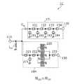
도 8e는 실시 형태 2의 변형예 3에 관한 멀티플렉서(3)의 회로 블록도이다. 도 8e에 도시한 바와 같이, 본 변형예에 관한 멀티플렉서(3)는, 로우 밴드용 필터(31L)와, 미들 밴드용 필터(32M)와, 하이 밴드용 필터(33H)와, 콘덴서 CBL 및 CBM과, 공통 단자(110)와, 입출력 단자(120, 130 및 140)와, 스위치(31s, 32s 및 33s)를 구비한다. 멀티플렉서(3)는 공통 단자(110)에 접속된 로우 밴드용 필터(31L), 미들 밴드용 필터(32M) 및 하이 밴드용 필터(33H)를 구비하는 복합 탄성파 필터 장치이다.8E is a circuit block diagram of the
본 변형예에 관한 멀티플렉서(3)는, 실시 형태 2에 관한 멀티플렉서(2)와 비교하여, 공통 단자(110)와, 로우 밴드용 필터(31L), 미들 밴드용 필터(32M), 및 하이 밴드용 필터(33H)를 연결하는 경로의 사이에, 각각, 스위치(31s, 32s 및 33s)가 배치되어 있는 점이 상이하다. 이하, 본 변형예에 관한 멀티플렉서(3)에 대하여, 실시 형태 2에 관한 멀티플렉서(2)와 상이한 구성만 설명한다.The
상기와 같이, 공통 단자(110)와 각 필터 사이에, 신호 경로의 도통 및 차단을 전환하는 스위치(31s, 32s 및 33s)가 배치됨으로써, 사용되는 주파수 대역(밴드)에 따라서 스위치(31s 내지 33s)를 제어함으로써, 스위치가 차단된 신호 경로의 필터의 반사 계수를 고려할 필요가 없어진다. 따라서, 각 필터의 통과 대역에 있어서의 삽입 손실을 개선하는 것이 가능해진다.As described above, between the
도 8f는 실시 형태 2의 변형예 3에 관한 멀티플렉서(3A)의 회로 구성도이다. 도 8f에 도시된 멀티플렉서(3A)는, 멀티플렉서(3)의 구체적 회로 구성을 예시한 것이다. 도 8f에 도시한 바와 같이, 멀티플렉서(3A)는, 로우 밴드용 필터(31L)와, 미들 밴드용 필터(32M)와, 하이 밴드용 필터(33H)와, 콘덴서 CB10 및 CB11과, 인덕터 LP9와, 공통 단자(110)와, 입출력 단자(120, 130 및 140)와, 스위치(31s, 32s 및 33s)를 구비한다.8F is a circuit configuration diagram of the
로우 밴드용 필터(31L)는, 실시 형태 2에 관한 로우 밴드용 필터(21L)와 동일한 구성을 갖는다. 로우 밴드용 필터(21L)의 각 SAW 공진자는, LiTaO3 기판을 사용한 리키파, 또는, LiNbO3 기판을 사용한 러브파를 이용하고 있다.The low-
미들 밴드용 필터(32M)는, 공통 단자(110)와 입출력 단자(130)를 연결하는 직렬 암에 접속된 종결합형 SAW 공진부(291 및 292)에 의해, 밴드 패스 필터를 구성하고 있다. 종결합형 SAW 공진부(291 및 292)를 구성하는 6개의 공진자는, SAW 공진자이다. 미들 밴드용 필터(32M)의 각 SAW 공진자는, LiTaO3 기판을 사용한 리키파, 또는, LiNbO3 기판을 사용한 러브파를 이용하고 있다.The
하이 밴드용 필터(33H)는, 실시 형태 2에 관한 하이 밴드용 필터(23H)와 동일한 구성을 갖고, 공통 단자(110)와 입출력 단자(130)를 연결하는 직렬 암에 접속된 직렬 암 공진자(301 내지 305)와, 상기 직렬 암과 그라운드 단자를 연결하는 병렬 암에 접속된 병렬 암 공진자(351 내지 354)에 의해, 래더형의 밴드 패스 필터를 구성하고 있다. 또한, 직렬 암 공진자(301 내지 305) 및 병렬 암 공진자(351 내지 354) 중, 공통 단자(110)에 가장 가깝게 접속되어 있는 것은 직렬 암 공진자(301)이다.The high-
콘덴서 CB10은, 멀티플렉서(3)에 있어서의 콘덴서 CBL이며, 콘덴서 CB11은, 멀티플렉서(3)에 있어서의 콘덴서 CBM이다.The capacitor CB10 is the capacitor CBL in the
인덕터 LP9는, 공통 단자(110)와 접지 단자 사이에 접속되어 있다. 이에 의해, 안테나 소자와 각 필터의 임피던스 정합을 확보할 수 있다.The inductor LP9 is connected between the
상기 구성과 같이, 공통 단자(110)와 각 필터 사이에, 신호 경로의 도통 및 차단을 전환하는 스위치(31s, 32s 및 33s)가 배치됨으로써, 사용되는 주파수 대역(밴드)에 따라서 스위치(31s 내지 33s)를 제어함으로써, 스위치가 차단된 신호 경로의 필터의 반사 계수를 고려할 필요가 없어진다. 따라서, 각 필터의 통과 대역에 있어서의 삽입 손실을 개선하는 것이 가능해진다.As described above, between the
(실시 형태 3)(Embodiment 3)
상기 실시 형태 1, 2 및 그 변형예에 관한 멀티플렉서는, 고주파 프론트 엔드 회로, 나아가 당해 고주파 프론트 엔드 회로를 구비하는 통신 장치에 적용할 수도 있다. 따라서, 본 실시 형태에서는, 이와 같은 고주파 프론트 엔드 회로 및 통신 장치에 대하여 설명한다.The multiplexers according to the first and second embodiments and modifications thereof can also be applied to a high-frequency front-end circuit and further to a communication device provided with the high-frequency front-end circuit. Therefore, in this embodiment, such a high-frequency front-end circuit and communication device will be described.
도 9는 실시 형태 3에 관한 고주파 프론트 엔드 회로(30) 및 통신 장치(40)의 회로 구성도이다. 또한, 도 9에는, 통신 장치(40)와 접속되는 안테나 소자(5)에 대해서도 아울러 도시되어 있다. 고주파 프론트 엔드 회로(30)와, RF 신호 처리 회로(RFIC)(6)와, 베이스 밴드 신호 처리 회로(BBIC)(7)는, 통신 장치(40)를 구성하고 있다.9 is a circuit configuration diagram of the high frequency
고주파 프론트 엔드 회로(30)는 멀티플렉서(1)와, 스위치(25)와, 로우 노이즈 앰프 회로(26)를 구비한다.The high frequency
멀티플렉서(1)는, 예를 들어 실시 형태 1에 관한 멀티플렉서(1)이다.The
스위치(25)는, 멀티플렉서(1)의 입출력 단자(120 및 130)에 개별로 접속된 2개의 선택 단자, 및, 로우 노이즈 앰프 회로(26)에 접속된 공통 단자를 갖는 스위치 회로이다. 스위치(25)는, 예를 들어 SPDT(Single Pole Double Throw)형의 스위치를 포함하고, 제어부(도시하지 않음)로부터의 제어 신호에 따라서, 공통 단자와 소정의 밴드에 대응하는 신호 경로를 접속한다. 또한, 공통 단자와 접속되는 선택 단자는 하나에 한정되지 않고, 복수여도 상관없다. 즉, 고주파 프론트 엔드 회로(30)는 캐리어 애그리게이션에 대응해도 상관없다.The
로우 노이즈 앰프 회로(26)는 안테나 소자(5), 멀티플렉서(1) 및 스위치(25)를 경유한 고주파 신호(여기서는 고주파 수신 신호)를 증폭하고, RF 신호 처리 회로(6)에 출력하는 수신 증폭 회로이다.The low-
RF 신호 처리 회로(6)는, 안테나 소자(5)로부터 수신 신호 경로를 통해 입력된 고주파 수신 신호를, 다운 컨버트 등에 의해 신호 처리하고, 당해 신호 처리하여 생성된 수신 신호를 베이스 밴드 신호 처리 회로(7)에 출력한다. RF 신호 처리 회로(6)는, 예를 들어 RFIC이다.The RF
베이스 밴드 신호 처리 회로(7)에서 처리된 신호는, 예를 들어 화상 신호로서 화상 표시를 위해, 또는, 음성 신호로서 통화를 위해 사용된다.The signal processed by the baseband
또한, 고주파 프론트 엔드 회로(30)는, 상술한 각 구성 요소의 사이에, 다른 회로 소자를 구비하고 있어도 된다.In addition, the high frequency
이상과 같이 구성된 고주파 프론트 엔드 회로(30) 및 통신 장치(40)에 의하면, 실시 형태 1, 2 또는 그 변형예에 관한 멀티플렉서를 구비함으로써, 각각의 필터의 전단에 분파/합파기나 위상 조정 회로 등을 배치하지 않더라도, 고주파 신호의 전파 손실을 저감할 수 있어, 소형화 및 저비용화가 가능해진다.According to the high-frequency front-
또한, 고주파 프론트 엔드 회로(30)는, 실시 형태 1에 관한 멀티플렉서(1) 대신에, 송신 및 수신의 양쪽이 가능한 트리플렉서 또는 쿼드플렉서를 구비해도 된다.In addition, the high frequency
또한, 통신 장치(40)는 고주파 신호의 처리 방식에 따라서, 베이스 밴드 신호 처리 회로(BBIC)(7)를 구비하고 있지 않아도 된다.In addition, the
(그 밖의 변형예 등)(Other modifications, etc.)
이상, 본 발명의 실시 형태에 관한 멀티플렉서, 고주파 프론트 엔드 회로 및 통신 장치에 대하여, 실시 형태 및 그 변형예를 들어 설명하였지만, 본 발명은 상기 실시 형태 및 변형예에 있어서의 임의의 구성 요소를 조합하여 실현되는 다른 실시 형태나, 상기 실시 형태에 대하여 본 발명의 주지를 일탈하지 않는 범위에서 당업자가 생각해 내는 각종 변형을 실시하여 얻어지는 변형예나, 본 발명에 관한 고주파 프론트 엔드 회로 및 통신 장치를 내장한 각종 기기도 본 발명에 포함된다.In the above, the multiplexer, the high frequency front end circuit and the communication device according to the embodiment of the present invention have been described with reference to the embodiment and its modifications, but the present invention combines any of the components in the above embodiments and modifications Other embodiments to be realized, modifications obtained by carrying out various modifications conceived by those skilled in the art without departing from the spirit of the present invention with respect to the above embodiments, and the high-frequency front-end circuit and communication device according to the present invention are incorporated. Various devices are also included in the present invention.
예를 들어, 상기 설명에서는, 멀티플렉서로서, 2개의 수신 신호 경로가 공통 단자에 접속된 2분파/합파 회로, 및, 3개의 수신 신호 경로 또는 송신 신호 경로가 공통 단자에 접속된 3분파/합파 회로를 예로 들어 설명하였지만, 본 발명은, 예를 들어 송신 경로 및 수신 경로의 양쪽을 포함하는 회로나 4개 이상의 신호 경로가 공통 단자에 접속된 분파/합파 회로에 대해서도 적용할 수 있다.For example, in the above description, as a multiplexer, a two-wave/harmonic circuit having two received signal paths connected to a common terminal, and a three-wave/harmonic circuit having three received signal paths or a transmitted signal path connected to a common terminal, Although the example has been described as an example, the present invention can be applied to, for example, a circuit including both a transmission path and a reception path, or a division/synthesis circuit in which four or more signal paths are connected to a common terminal.
즉, 중심 주파수가 f1, f2, …, fn(n은 2 이상의 자연수)인 (n개의) 필터가 공통 단자에 접속된 멀티플렉서로서, 중심 주파수가 가장 높은 fn을 구성하는 필터(제2 필터) 이외의 필터 중 적어도 하나인 제1 필터에 있어서, 공통 단자와 제1 필터를 연결하는 접속 경로(직렬 암)에 콘덴서가 직렬 배치되어 있다. 여기서, 상기 콘덴서의 제2 필터의 통과 대역(제2 통과 대역)에 있어서의 Q값은, 제1 필터의 SAW 공진자를 용량으로서 본 경우의 제2 통과 대역에 있어서의 용량 Q값보다도 높다. 바꾸어 말하면, 콘덴서는, 제1 필터의 SAW 공진자의 제2 통과 대역에 있어서의 벌크파 방사 손실을 보상하는 기능을 갖는다.That is, the center frequencies are f1, f2,… , fn (n is a natural number greater than or equal to 2) is a multiplexer with (n) filters connected to a common terminal, to a first filter that is at least one of filters other than the filter (second filter) constituting fn having the highest center frequency. In this case, capacitors are arranged in series in a connection path (serial arm) connecting the common terminal and the first filter. Here, the Q value in the pass band (second pass band) of the second filter of the capacitor is higher than the capacity Q value in the second pass band when the SAW resonator of the first filter is viewed as a capacity. In other words, the condenser has a function of compensating for the bulk wave emission loss in the second pass band of the SAW resonator of the first filter.
이에 의해, 제1 필터의 제2 통과 대역에 있어서의 반사 계수(|Γ|)를 올릴(리턴 로스를 저감할) 수 있으므로, 제1 필터와 함께 공통 단자에 접속된 제2 필터의 제2 통과 대역에 있어서의 삽입 손실을 개선하는 것이 가능해진다. 따라서, 각각의 필터의 전단에 분파/합파기나 위상 조정 회로 등을 배치하지 않더라도 고주파 신호의 전파 손실을 저감할 수 있어, 소형화 및 저비용화가 가능해진다.Thereby, since the reflection coefficient (|Γ|) in the second pass band of the first filter can be increased (return loss is reduced), the second pass of the second filter connected to the common terminal together with the first filter It becomes possible to improve the insertion loss in the band. Accordingly, propagation loss of a high-frequency signal can be reduced even if a branch/synthesizer, a phase adjustment circuit, or the like is not disposed at the front end of each filter, so that miniaturization and cost reduction are possible.
또한, 상기 실시 형태에서는, 멀티플렉서에 사용되는 주파수 대역(밴드)으로서, LTE 규격의 Band1 및 Band11을 예시하였지만, 이것에 한정되지 않는다.In the above embodiments, Band1 and Band11 of the LTE standard are illustrated as frequency bands (bands) used in the multiplexer, but are not limited to this.
또한, 상기 실시 형태에 있어서, 2 이상의 필터가 공통 단자에 접속되어 있다란, 당해 2 이상의 필터가 공통 단자에 직접 접속되어 있는 구성만을 나타내는 것이 아니라, 당해 2 이상의 필터가, 이하와 같은 구성에 의해, 공통 단자에 간접적으로 접속되어 있는 구성을 포함하는 것으로 한다. 예를 들어, 공통 단자와 2 이상의 필터 사이에, 1 이상의 도통이 얻어지는 스위치, 위상 회로 또는 분배기(디바이더)와 같은 분기 회로가 배치되어 있는 구성을 들 수 있다.In addition, in the said embodiment, that two or more filters are connected to the common terminal does not show only the structure in which the said two or more filters are directly connected to the common terminal, but the two or more filters are comprised by the following structures. It is assumed to include a configuration indirectly connected to the common terminal. For example, there is a configuration in which a branch circuit such as a switch, a phase circuit, or a divider (divider) in which one or more conduction is obtained is disposed between a common terminal and two or more filters.
또한, 멀티플렉서가 갖는 각 필터에 있어서, 또한, 입출력 단자 및 접지 단자 등의 각 단자의 사이에, 인덕터나 캐패시터가 접속되어 있어도 되고, 저항 소자 등의 인덕터 및 캐패시터 이외의 회로 소자가 부가되어 있어도 된다.In addition, in each filter of the multiplexer, an inductor or a capacitor may be connected between each terminal such as an input/output terminal and a ground terminal, and a circuit element other than an inductor and a capacitor such as a resistance element may be added. .
본 발명은, 멀티 밴드화 및 멀티 모드화된 주파수 규격에 적용할 수 있는 저손실, 소형 및 저비용의 멀티플렉서, 고주파 프론트 엔드 회로 및 통신 장치로서, 휴대 전화 등의 통신 기기에 널리 이용할 수 있다.The present invention is a low-loss, small and low-cost multiplexer, high-frequency front-end circuit and communication device applicable to multi-banded and multi-mode frequency standards, and can be widely used in communication devices such as mobile phones.
1, 1A, 1B, 1C, 2, 2A, 2B, 2C, 600 : 멀티플렉서
5 : 안테나 소자
6 : RF 신호 처리 회로(RFIC)
7 : 베이스 밴드 신호 처리 회로(BBIC)
11L, 13L, 15L, 17L, 611L : 저주파측 필터
12H, 16H, 18H, 612H : 고주파측 필터
21L : 로우 밴드용 필터
22M : 미들 밴드용 필터
23H : 하이 밴드용 필터
25 : 스위치
26 : 로우 노이즈 앰프 회로
30 : 고주파 프론트 엔드 회로
40 : 통신 장치
100 : 기판
101, 102, 103, 104, 105, 111, 112, 113, 114, 121, 122, 131, 132, 133, 134, 201, 202, 203, 204, 205, 211, 212, 213, 221, 222, 223, 241, 242, 243, 244, 245, 301, 302, 303, 304, 305 : 직렬 암 공진자
110 : 공통 단자
120, 130, 140 : 입출력 단자
125, 215, 225 : 종결합형 SAW 공진부
151, 152, 153, 154, 161, 162, 163, 164, 171, 181, 182, 183, 184, 251, 252, 253, 254, 261, 271, 281, 282, 283, 284, 351, 352, 353, 354 : 병렬 암 공진자
CB1, CB2, CB3, CB4, CB5, CB6, CB7, CB8, CB9, CBL, CBM : 콘덴서
LP1, LP2, LP3, LP4, LP5, LP6, LP7, LP8 : 인덕터1, 1A, 1B, 1C, 2, 2A, 2B, 2C, 600: multiplexer
5: antenna element
6: RF signal processing circuit (RFIC)
7: Baseband signal processing circuit (BBIC)
11L, 13L, 15L, 17L, 611L: Low-frequency filter
12H, 16H, 18H, 612H: High-frequency filter
21L: Low band filter
22M: Middle band filter
23H: High band filter
25: switch
26: low noise amplifier circuit
30: high frequency front end circuit
40: communication device
100: substrate
101, 102, 103, 104, 105, 111, 112, 113, 114, 121, 122, 131, 132, 133, 134, 201, 202, 203, 204, 205, 211, 212, 213, 221, 222, 223, 241, 242, 243, 244, 245, 301, 302, 303, 304, 305: series arm resonator
110: common terminal
120, 130, 140: input/output terminal
125, 215, 225: longitudinally coupled SAW resonator
151, 152, 153, 154, 161, 162, 163, 164, 171, 181, 182, 183, 184, 251, 252, 253, 254, 261, 271, 281, 282, 283, 284, 351, 352, 353, 354: parallel arm resonator
CB1 , CB2 , CB3 , CB4 , CB5 , CB6 , CB7 , CB8 , CB9 , CBL , CBM : Condenser
LP1 , LP2 , LP3 , LP4 , LP5 , LP6 , LP7 , LP8 : Inductor
Claims (11)
Translated fromKorean상기 공통 단자와 상기 제1 입출력 단자 사이에 배치된 1 이상의 탄성 표면파 공진자를 포함하고, 제1 통과 대역을 갖는 제1 필터와,
상기 공통 단자 및 상기 제2 입출력 단자에 접속되며, 상기 제1 통과 대역보다도 주파수가 높은 제2 통과 대역을 갖는 제2 필터와,
상기 공통 단자와 상기 제1 필터의 접속 경로에 직렬로 배치된 콘덴서를 구비하고,
상기 제1 필터는, 상기 1 이상의 탄성 표면파 공진자를 구성하는 IDT 전극이 형성된, 적어도 일부에 압전성을 갖는 기판을 갖고,
상기 콘덴서는, 서로 대향하는 빗형 전극에 의해 상기 기판 상에 형성되고,
상기 콘덴서의 상기 빗형 전극을 구성하는 복수의 전극 핑거의 피치는, 상기 IDT 전극을 구성하는 복수의 전극 핑거의 피치보다도 작고,
상기 콘덴서의 상기 복수의 전극 핑거의 방향은 상기 IDT 전극을 구성하는 상기 복수의 전극 핑거의 방향과 교차하고,
상기 콘덴서의 상기 제2 통과 대역에 있어서의 Q값은, 상기 1 이상의 탄성 표면파 공진자를 용량으로서 본 경우의 상기 제2 통과 대역에 있어서의 상기 용량의 Q값보다도 높은 멀티플렉서.A multiplexer having a common terminal, a first input/output terminal and a second input/output terminal, and having a plurality of filters connected to the common terminal,
A first filter including at least one surface acoustic wave resonator disposed between the common terminal and the first input/output terminal, and having a first pass band,
A second filter connected to the common terminal and the second input/output terminal, and having a second pass band having a higher frequency than the first pass band;
And a capacitor arranged in series in a connection path between the common terminal and the first filter,
The first filter has a substrate having piezoelectric properties at least in part on which an IDT electrode constituting the one or more surface acoustic wave resonators is formed,
The capacitor is formed on the substrate by comb-shaped electrodes facing each other,
The pitch of the plurality of electrode fingers constituting the comb-shaped electrode of the condenser is smaller than the pitch of the plurality of electrode fingers constituting the IDT electrode,
The direction of the plurality of electrode fingers of the capacitor intersects the direction of the plurality of electrode fingers constituting the IDT electrode,
A multiplexer having a Q value in the second pass band of the capacitor higher than the Q value of the capacity in the second pass band when the one or more surface acoustic wave resonators are viewed as capacitance.
상기 공통 단자와 상기 제1 입출력 단자 사이에 배치된 1 이상의 탄성 표면파 공진자를 포함하고, 제1 통과 대역을 갖는 제1 필터와,
상기 공통 단자 및 상기 제2 입출력 단자에 접속되며, 상기 제1 통과 대역보다도 주파수가 높은 제2 통과 대역을 갖는 제2 필터와,
상기 공통 단자와 상기 제1 필터의 접속 경로에 직렬로 배치되며, 상기 1 이상의 탄성 표면파 공진자의 상기 제2 통과 대역에 있어서의 벌크파 방사 손실을 보상하기 위한 콘덴서를 구비하고,
상기 콘덴서는, 다층 기판 내의 복수층으로 형성되어 있거나 상기 다층 기판 내에 배치된 칩 콘덴서이며,
상기 다층 기판은 상기 제1 필터 및 상기 제2 필터를 실장함과 함께, 상기 제1 필터와 상기 제2 필터를 접속하는 배선을 포함하고,
상기 콘덴서의 상기 제2 통과 대역에 있어서의 Q값은, 상기 1 이상의 탄성 표면파 공진자를 용량으로서 본 경우의 상기 제2 통과 대역에 있어서의 상기 용량의 Q값보다도 높은 멀티플렉서.A multiplexer having a common terminal, a first input/output terminal and a second input/output terminal, and having a plurality of filters connected to the common terminal,
A first filter including at least one surface acoustic wave resonator disposed between the common terminal and the first input/output terminal, and having a first pass band,
A second filter connected to the common terminal and the second input/output terminal, and having a second pass band having a higher frequency than the first pass band;
It is arranged in series in the connection path of the common terminal and the first filter, and is provided with a capacitor for compensating for the bulk wave radiation loss in the second pass band of the at least one surface acoustic wave resonator,
The capacitor is a chip capacitor formed of a plurality of layers in a multilayer substrate or disposed in the multilayer substrate,
The multi-layer substrate includes wirings connecting the first filter and the second filter while mounting the first filter and the second filter,
A multiplexer having a Q value in the second pass band of the capacitor higher than the Q value of the capacity in the second pass band when the one or more surface acoustic wave resonators are viewed as capacitance.
상기 제1 필터의 상기 1 이상의 탄성 표면파 공진자에서는, LiTaO3를 포함하는 압전성의 기판에서 전파되는 리키파가 탄성 표면파로서 이용되는 멀티플렉서.The method according to claim 1 or 2,
In the one or more surface acoustic wave resonators of the first filter, a multiplexer in which Ricky waves propagated from a piezoelectric substrate containing LiTaO3 are used as surface acoustic waves.
상기 제1 필터의 상기 1 이상의 탄성 표면파 공진자에서는, LiNbO3를 포함하는 압전성의 기판에서 전파되는 러브파가 탄성 표면파로서 이용되는 멀티플렉서.The method according to claim 1 or 2,
In the one or more surface acoustic wave resonators of the first filter, a love wave propagated from a piezoelectric substrate containing LiNbO3 is used as a multiplexer.
제3 입출력 단자를 더 구비하고,
상기 공통 단자와 상기 제3 입출력 단자 사이에 배치된 1 이상의 탄성 표면파 공진자를 포함하고, 상기 제2 통과 대역보다도 주파수가 낮은 제3 통과 대역을 갖는 제3 필터를 구비하고,
상기 제3 필터의 상기 1 이상의 탄성 표면파 공진자에서는, LiNbO3를 포함하는 압전성의 기판에서 전파되는 레일리파가 탄성 표면파로서 이용되고,
상기 공통 단자와 상기 제3 필터의 접속 경로에는, 콘덴서가 직렬 배치되어 있지 않은 멀티플렉서.The method according to claim 1 or 2,
A third input/output terminal is further provided.
A third filter including at least one surface acoustic wave resonator disposed between the common terminal and the third input/output terminal, and having a third pass band having a frequency lower than that of the second pass band,
In the one or more surface acoustic wave resonators of the third filter, a Rayleigh wave propagated from a piezoelectric substrate containing LiNbO3 is used as the surface acoustic wave,
A multiplexer in which capacitors are not arranged in series in the connection path between the common terminal and the third filter.
상기 공통 단자와 상기 복수의 필터 사이에, 신호 경로의 도통 및 차단을 전환하는 스위치를 더 구비하는 멀티플렉서.The method according to claim 1 or 2,
A multiplexer further comprising a switch for switching between conduction and interruption of the signal path between the common terminal and the plurality of filters.
상기 공통 단자와 접지 단자 사이에 접속된 인덕터를 더 구비하는 멀티플렉서.The method according to claim 1 or 2,
A multiplexer further comprising an inductor connected between the common terminal and the ground terminal.
상기 멀티플렉서에 접속된 증폭 회로를 구비하는 고주파 프론트 엔드 회로.The multiplexer according to claim 1 or 2,
A high frequency front end circuit comprising an amplifying circuit connected to the multiplexer.
상기 안테나 소자와 상기 RF 신호 처리 회로 사이에서 상기 고주파 신호를 전달하는 제10항에 기재된 고주파 프론트 엔드 회로를 구비하는 통신 장치.RF signal processing circuit for processing a high-frequency signal transmitted and received by the antenna element,
A communication device comprising the high frequency front end circuit according to claim 10 for transmitting the high frequency signal between the antenna element and the RF signal processing circuit.
Applications Claiming Priority (3)
| Application Number | Priority Date | Filing Date | Title |
|---|---|---|---|
| JP2016118399 | 2016-06-14 | ||
| JPJP-P-2016-118399 | 2016-06-14 | ||
| PCT/JP2017/019261WO2017217197A1 (en) | 2016-06-14 | 2017-05-23 | Multiplexer, high-frequency front end circuit, and communication device |
Publications (2)
| Publication Number | Publication Date |
|---|---|
| KR20190002698A KR20190002698A (en) | 2019-01-08 |
| KR102134087B1true KR102134087B1 (en) | 2020-07-14 |
Family
ID=60663071
Family Applications (1)
| Application Number | Title | Priority Date | Filing Date |
|---|---|---|---|
| KR1020187035919AActiveKR102134087B1 (en) | 2016-06-14 | 2017-05-23 | Multiplexer, high frequency front end circuit and communication device |
Country Status (5)
| Country | Link |
|---|---|
| US (3) | US10637439B2 (en) |
| JP (1) | JPWO2017217197A1 (en) |
| KR (1) | KR102134087B1 (en) |
| CN (1) | CN109417378B (en) |
| WO (1) | WO2017217197A1 (en) |
Families Citing this family (15)
| Publication number | Priority date | Publication date | Assignee | Title |
|---|---|---|---|---|
| CN109196784B (en)* | 2016-05-27 | 2020-07-28 | 株式会社村田制作所 | Multiplexer, high-frequency front-end circuit, and communication device |
| JP6798866B2 (en)* | 2016-12-15 | 2020-12-09 | 京セラ株式会社 | Multiplexer |
| JP6835005B2 (en)* | 2018-02-16 | 2021-02-24 | 株式会社村田製作所 | Front end circuit |
| KR102605779B1 (en)* | 2018-05-14 | 2023-11-24 | 가부시키가이샤 무라타 세이사쿠쇼 | Multiplexers, high-frequency front-end circuits and communication devices |
| WO2020003956A1 (en)* | 2018-06-28 | 2020-01-02 | 株式会社村田製作所 | Multiplexer, high-frequency front end circuit, and communications device |
| JP2020043380A (en) | 2018-09-06 | 2020-03-19 | 株式会社村田製作所 | Filter and multiplexer |
| EP3742678B1 (en)* | 2019-05-24 | 2022-02-23 | NXP USA, Inc. | Integrated circuit with physical layer interface circuit |
| JP7218807B2 (en)* | 2019-06-24 | 2023-02-07 | 株式会社村田製作所 | Composite filter device |
| JP7415261B2 (en)* | 2019-09-18 | 2024-01-17 | 株式会社村田製作所 | filter device |
| CN114641937B (en)* | 2019-11-20 | 2023-08-08 | 株式会社村田制作所 | High-frequency circuit, high-frequency front-end circuit, and communication device |
| CN111211754B (en)* | 2020-02-12 | 2021-02-26 | 诺思(天津)微系统有限责任公司 | Method for adjusting FBAR parasitic component, filter, multiplexer and communication equipment |
| JP2021141500A (en)* | 2020-03-06 | 2021-09-16 | 株式会社村田製作所 | SAW filter device and multiplexer using it |
| JP2021164142A (en) | 2020-04-03 | 2021-10-11 | 株式会社村田製作所 | High frequency module, high frequency circuit and communication device |
| US20220200645A1 (en)* | 2020-12-18 | 2022-06-23 | Skyworks Solutions, Inc. | Stacked resonator based antennaplexer |
| US20220376676A1 (en)* | 2021-05-18 | 2022-11-24 | Chengdu Pinnacle Microwave Co., Ltd. | High-isolation and anti-glue-invasion saw duplexer |
Citations (5)
| Publication number | Priority date | Publication date | Assignee | Title |
|---|---|---|---|---|
| WO2009147787A1 (en)* | 2008-06-06 | 2009-12-10 | パナソニック株式会社 | Acoustic wave duplexer |
| WO2012098816A1 (en)* | 2011-01-18 | 2012-07-26 | 株式会社村田製作所 | Elastic surface wave filter device |
| WO2015098756A1 (en)* | 2013-12-26 | 2015-07-02 | 株式会社村田製作所 | Elastic wave device and filter apparatus |
| JP2015201808A (en)* | 2014-04-10 | 2015-11-12 | 太陽誘電株式会社 | Multiplexer |
| WO2016013659A1 (en)* | 2014-07-25 | 2016-01-28 | 株式会社村田製作所 | Bandpass filter and filter module |
Family Cites Families (28)
| Publication number | Priority date | Publication date | Assignee | Title |
|---|---|---|---|---|
| JPS63260213A (en)* | 1986-09-12 | 1988-10-27 | Hiroshi Shimizu | Resonator using high coupling love wave type saw substrate |
| JP3126416B2 (en)* | 1991-06-26 | 2001-01-22 | キンセキ株式会社 | Surface acoustic wave device |
| JPH0522074A (en)* | 1991-07-11 | 1993-01-29 | Hitachi Ltd | Surface acoustic wave resonator, surface acoustic wave resonator composite filter, and wireless transceiver |
| JPH1131905A (en)* | 1997-07-14 | 1999-02-02 | Matsushita Electric Ind Co Ltd | Duplexer, duplexer using the same, and mobile communication device for dual frequency band |
| JP2000216661A (en)* | 1999-01-26 | 2000-08-04 | Oki Electric Ind Co Ltd | Receiving band division type surface acoustic wave branching filter |
| US6690251B2 (en)* | 2001-04-11 | 2004-02-10 | Kyocera Wireless Corporation | Tunable ferro-electric filter |
| JP2003060483A (en)* | 2001-06-05 | 2003-02-28 | Murata Mfg Co Ltd | Surface acoustic wave device and manufacturing method therefor, and communication device |
| JP2003188675A (en)* | 2001-12-19 | 2003-07-04 | Alps Electric Co Ltd | Surface acoustic wave element and duplexer provided therewith |
| JP2003283363A (en) | 2002-03-27 | 2003-10-03 | Nrs Technology Kk | Antenna duplexer |
| JP2004140696A (en)* | 2002-10-18 | 2004-05-13 | Hitachi Metals Ltd | High frequency switching circuit and antenna switching module using the same, antenna switching layered module and communication equipment |
| JP2004140738A (en)* | 2002-10-21 | 2004-05-13 | Toyo Commun Equip Co Ltd | Surface acoustic wave filter |
| US7023297B2 (en)* | 2003-05-14 | 2006-04-04 | Murata Manufacturing Co., Ltd. | Surface acoustic wave branching filter |
| JP2005045432A (en)* | 2003-07-25 | 2005-02-17 | Toyo Commun Equip Co Ltd | Surface acoustic wave device |
| JP2005072805A (en)* | 2003-08-21 | 2005-03-17 | Murata Mfg Co Ltd | Duplexer |
| CN100530958C (en)* | 2003-10-16 | 2009-08-19 | 京瓷株式会社 | Composite channel splitting circuit, chip element using same, high-frequency model and wireless communication apparatus |
| JP4259576B2 (en)* | 2004-03-12 | 2009-04-30 | 株式会社村田製作所 | Duplexer and surface acoustic wave filter |
| JP2006211057A (en)* | 2005-01-25 | 2006-08-10 | Oki Electric Ind Co Ltd | Triplexer |
| US8145155B2 (en)* | 2005-09-06 | 2012-03-27 | Mediatek, Inc. | Passive mixer and high Q RF filter using a passive mixer |
| US9106316B2 (en)* | 2005-10-24 | 2015-08-11 | Parkervision, Inc. | Systems and methods of RF power transmission, modulation, and amplification |
| JP4871966B2 (en)* | 2009-01-30 | 2012-02-08 | 太陽誘電株式会社 | High frequency device, filter, duplexer, communication module, communication device |
| JP5582400B2 (en) | 2010-09-30 | 2014-09-03 | 日立金属株式会社 | High-frequency circuit component and communication device |
| JP5672050B2 (en) | 2011-02-21 | 2015-02-18 | 株式会社村田製作所 | Surface acoustic wave filter device |
| JPWO2013021626A1 (en)* | 2011-08-08 | 2015-03-05 | パナソニック株式会社 | Filter module |
| US9667306B2 (en)* | 2011-10-26 | 2017-05-30 | Adam James Wang | Multimode multiband wireless device with broadband power amplifier |
| KR101479962B1 (en)* | 2013-04-26 | 2015-01-08 | 주식회사 아이.티.에프 | Variable Bandpass Filter Device and Mobile Communication Repeater |
| JP6142924B2 (en)* | 2013-08-21 | 2017-06-07 | 株式会社村田製作所 | Tunable filter |
| DE112014006120B4 (en) | 2014-01-07 | 2021-07-01 | Murata Manufacturing Co., Ltd. | Filter device |
| JP6652062B2 (en)* | 2014-09-30 | 2020-02-19 | 株式会社村田製作所 | Elastic wave device and method of manufacturing the same |
- 2017
- 2017-05-23KRKR1020187035919Apatent/KR102134087B1/enactiveActive
- 2017-05-23WOPCT/JP2017/019261patent/WO2017217197A1/ennot_activeCeased
- 2017-05-23CNCN201780036473.9Apatent/CN109417378B/enactiveActive
- 2017-05-23JPJP2018523615Apatent/JPWO2017217197A1/enactivePending
- 2018
- 2018-12-12USUS16/217,254patent/US10637439B2/enactiveActive
- 2020
- 2020-03-20USUS16/824,773patent/US10972073B2/enactiveActive
- 2021
- 2021-01-22USUS17/156,039patent/US11336261B2/enactiveActive
Patent Citations (5)
| Publication number | Priority date | Publication date | Assignee | Title |
|---|---|---|---|---|
| WO2009147787A1 (en)* | 2008-06-06 | 2009-12-10 | パナソニック株式会社 | Acoustic wave duplexer |
| WO2012098816A1 (en)* | 2011-01-18 | 2012-07-26 | 株式会社村田製作所 | Elastic surface wave filter device |
| WO2015098756A1 (en)* | 2013-12-26 | 2015-07-02 | 株式会社村田製作所 | Elastic wave device and filter apparatus |
| JP2015201808A (en)* | 2014-04-10 | 2015-11-12 | 太陽誘電株式会社 | Multiplexer |
| WO2016013659A1 (en)* | 2014-07-25 | 2016-01-28 | 株式会社村田製作所 | Bandpass filter and filter module |
Also Published As
| Publication number | Publication date |
|---|---|
| KR20190002698A (en) | 2019-01-08 |
| JPWO2017217197A1 (en) | 2019-03-22 |
| US20190123722A1 (en) | 2019-04-25 |
| WO2017217197A1 (en) | 2017-12-21 |
| US10637439B2 (en) | 2020-04-28 |
| CN109417378A (en) | 2019-03-01 |
| US20210143797A1 (en) | 2021-05-13 |
| US10972073B2 (en) | 2021-04-06 |
| US20200220523A1 (en) | 2020-07-09 |
| US11336261B2 (en) | 2022-05-17 |
| CN109417378B (en) | 2023-03-14 |
Similar Documents
| Publication | Publication Date | Title |
|---|---|---|
| KR102134087B1 (en) | Multiplexer, high frequency front end circuit and communication device | |
| US10727805B2 (en) | Multiplexer including filters with resonators and parallel inductor | |
| US12199657B2 (en) | High frequency filter, multiplexer, high frequency front-end circuit, and communication device | |
| CN109286387B (en) | High-frequency filter, multiplexer, high-frequency pre-circuit, and communication device | |
| US10700666B2 (en) | Filter circuit, multiplexer, and module | |
| JP6669681B2 (en) | Filter circuits, multiplexers and modules | |
| CN112740549B (en) | Multiplexer and high-frequency front-end circuit and communication device using the same | |
| US10651821B2 (en) | Multiplexer, high-frequency front-end circuit, and communication apparatus | |
| KR102312057B1 (en) | Multiplexer | |
| KR102193508B1 (en) | Seismic filter device, high frequency front end circuit and communication device | |
| JP2013258516A (en) | Filter module and duplexer module | |
| WO2020008759A1 (en) | High-frequency filter, multiplexer, high-frequency front-end circuit, and communication device | |
| JP2018129680A (en) | Filter circuits, multiplexers and modules | |
| KR102217491B1 (en) | Filter and multiplexer | |
| KR102309055B1 (en) | Filter and multiplexer | |
| JP2021072563A (en) | Multiplexer | |
| WO2020080017A1 (en) | High-frequency module | |
| US11901879B2 (en) | Multiplexer, radio-frequency front end circuit, and communication device | |
| KR20210011330A (en) | Filter and multiplexer |
Legal Events
| Date | Code | Title | Description |
|---|---|---|---|
| A201 | Request for examination | ||
| PA0105 | International application | Patent event date:20181211 Patent event code:PA01051R01D Comment text:International Patent Application | |
| PA0201 | Request for examination | Patent event code:PA02012R01D Patent event date:20181211 Comment text:Request for Examination of Application | |
| PG1501 | Laying open of application | ||
| E902 | Notification of reason for refusal | ||
| PE0902 | Notice of grounds for rejection | Comment text:Notification of reason for refusal Patent event date:20191029 Patent event code:PE09021S01D | |
| E701 | Decision to grant or registration of patent right | ||
| PE0701 | Decision of registration | Patent event code:PE07011S01D Comment text:Decision to Grant Registration Patent event date:20200410 | |
| GRNT | Written decision to grant | ||
| PR0701 | Registration of establishment | Comment text:Registration of Establishment Patent event date:20200708 Patent event code:PR07011E01D | |
| PR1002 | Payment of registration fee | Payment date:20200708 End annual number:3 Start annual number:1 | |
| PG1601 | Publication of registration | ||
| PR1001 | Payment of annual fee | Payment date:20240627 Start annual number:5 End annual number:5 |