KR102132512B1 - Camera module with compression-molded circuit board and manufacturing method thereof - Google Patents
Camera module with compression-molded circuit board and manufacturing method thereofDownload PDFInfo
- Publication number
- KR102132512B1 KR102132512B1KR1020170021007AKR20170021007AKR102132512B1KR 102132512 B1KR102132512 B1KR 102132512B1KR 1020170021007 AKR1020170021007 AKR 1020170021007AKR 20170021007 AKR20170021007 AKR 20170021007AKR 102132512 B1KR102132512 B1KR 102132512B1
- Authority
- KR
- South Korea
- Prior art keywords
- circuit board
- camera module
- compression
- molding
- molding die
- Prior art date
- Legal status (The legal status is an assumption and is not a legal conclusion. Google has not performed a legal analysis and makes no representation as to the accuracy of the status listed.)
- Active
Links
- 238000004519manufacturing processMethods0.000titleclaimsdescription15
- 238000000748compression mouldingMethods0.000claimsabstractdescription18
- 230000006835compressionEffects0.000claimsabstractdescription16
- 238000007906compressionMethods0.000claimsabstractdescription16
- 239000000463materialSubstances0.000claimsdescription35
- 238000000465mouldingMethods0.000claimsdescription23
- 238000000034methodMethods0.000claimsdescription22
- 229920005989resinPolymers0.000claimsdescription22
- 239000011347resinSubstances0.000claimsdescription22
- 230000003287optical effectEffects0.000claimsdescription20
- 239000012530fluidSubstances0.000claimsdescription17
- 230000003014reinforcing effectEffects0.000claimsdescription11
- 239000003822epoxy resinSubstances0.000claimsdescription7
- 229920000647polyepoxidePolymers0.000claimsdescription7
- 238000001125extrusionMethods0.000claimsdescription3
- 239000012943hotmeltSubstances0.000claims4
- 239000000155meltSubstances0.000claims2
- 238000010438heat treatmentMethods0.000claims1
- 230000002787reinforcementEffects0.000claims1
- 230000010354integrationEffects0.000abstractdescription3
- 239000000843powderSubstances0.000description4
- 238000005516engineering processMethods0.000description3
- 238000012986modificationMethods0.000description3
- 230000004048modificationEffects0.000description3
- 239000003990capacitorSubstances0.000description2
- 238000002844meltingMethods0.000description2
- 239000012768molten materialSubstances0.000description2
- 230000008569processEffects0.000description2
- RYGMFSIKBFXOCR-UHFFFAOYSA-NCopperChemical compound[Cu]RYGMFSIKBFXOCR-UHFFFAOYSA-N0.000description1
- 238000006243chemical reactionMethods0.000description1
- 229910052802copperInorganic materials0.000description1
- 239000010949copperSubstances0.000description1
- 238000009713electroplatingMethods0.000description1
- LNEPOXFFQSENCJ-UHFFFAOYSA-NhaloperidolChemical compoundC1CC(O)(C=2C=CC(Cl)=CC=2)CCN1CCCC(=O)C1=CC=C(F)C=C1LNEPOXFFQSENCJ-UHFFFAOYSA-N0.000description1
- 238000001192hot extrusionMethods0.000description1
- 230000006872improvementEffects0.000description1
- 230000008018meltingEffects0.000description1
- ICFJFFQQTFMIBG-UHFFFAOYSA-NphenforminChemical compoundNC(=N)NC(=N)NCCC1=CC=CC=C1ICFJFFQQTFMIBG-UHFFFAOYSA-N0.000description1
- 150000003071polychlorinated biphenylsChemical class0.000description1
- 238000003825pressingMethods0.000description1
- 230000009467reductionEffects0.000description1
- 238000005476solderingMethods0.000description1
- 229920001187thermosetting polymerPolymers0.000description1
Images


Classifications
- G—PHYSICS
- G02—OPTICS
- G02B—OPTICAL ELEMENTS, SYSTEMS OR APPARATUS
- G02B7/00—Mountings, adjusting means, or light-tight connections, for optical elements
- G02B7/02—Mountings, adjusting means, or light-tight connections, for optical elements for lenses
- G02B7/04—Mountings, adjusting means, or light-tight connections, for optical elements for lenses with mechanism for focusing or varying magnification
- G02B7/09—Mountings, adjusting means, or light-tight connections, for optical elements for lenses with mechanism for focusing or varying magnification adapted for automatic focusing or varying magnification
- H—ELECTRICITY
- H05—ELECTRIC TECHNIQUES NOT OTHERWISE PROVIDED FOR
- H05K—PRINTED CIRCUITS; CASINGS OR CONSTRUCTIONAL DETAILS OF ELECTRIC APPARATUS; MANUFACTURE OF ASSEMBLAGES OF ELECTRICAL COMPONENTS
- H05K1/00—Printed circuits
- H05K1/18—Printed circuits structurally associated with non-printed electric components
- H05K1/182—Printed circuits structurally associated with non-printed electric components associated with components mounted in the printed circuit board, e.g. insert mounted components [IMC]
- H05K1/185—Components encapsulated in the insulating substrate of the printed circuit or incorporated in internal layers of a multilayer circuit
- H—ELECTRICITY
- H05—ELECTRIC TECHNIQUES NOT OTHERWISE PROVIDED FOR
- H05K—PRINTED CIRCUITS; CASINGS OR CONSTRUCTIONAL DETAILS OF ELECTRIC APPARATUS; MANUFACTURE OF ASSEMBLAGES OF ELECTRICAL COMPONENTS
- H05K1/00—Printed circuits
- H05K1/02—Details
- H05K1/0296—Conductive pattern lay-out details not covered by sub groups H05K1/02 - H05K1/0295
- H05K1/0298—Multilayer circuits
- H—ELECTRICITY
- H04—ELECTRIC COMMUNICATION TECHNIQUE
- H04N—PICTORIAL COMMUNICATION, e.g. TELEVISION
- H04N23/00—Cameras or camera modules comprising electronic image sensors; Control thereof
- H04N23/50—Constructional details
- G—PHYSICS
- G03—PHOTOGRAPHY; CINEMATOGRAPHY; ANALOGOUS TECHNIQUES USING WAVES OTHER THAN OPTICAL WAVES; ELECTROGRAPHY; HOLOGRAPHY
- G03B—APPARATUS OR ARRANGEMENTS FOR TAKING PHOTOGRAPHS OR FOR PROJECTING OR VIEWING THEM; APPARATUS OR ARRANGEMENTS EMPLOYING ANALOGOUS TECHNIQUES USING WAVES OTHER THAN OPTICAL WAVES; ACCESSORIES THEREFOR
- G03B3/00—Focusing arrangements of general interest for cameras, projectors or printers
- G03B3/02—Focusing arrangements of general interest for cameras, projectors or printers moving lens along baseboard
- H—ELECTRICITY
- H04—ELECTRIC COMMUNICATION TECHNIQUE
- H04N—PICTORIAL COMMUNICATION, e.g. TELEVISION
- H04N23/00—Cameras or camera modules comprising electronic image sensors; Control thereof
- H04N23/50—Constructional details
- H04N23/51—Housings
- H—ELECTRICITY
- H04—ELECTRIC COMMUNICATION TECHNIQUE
- H04N—PICTORIAL COMMUNICATION, e.g. TELEVISION
- H04N23/00—Cameras or camera modules comprising electronic image sensors; Control thereof
- H04N23/50—Constructional details
- H04N23/54—Mounting of pick-up tubes, electronic image sensors, deviation or focusing coils
- H—ELECTRICITY
- H04—ELECTRIC COMMUNICATION TECHNIQUE
- H04N—PICTORIAL COMMUNICATION, e.g. TELEVISION
- H04N23/00—Cameras or camera modules comprising electronic image sensors; Control thereof
- H04N23/50—Constructional details
- H04N23/55—Optical parts specially adapted for electronic image sensors; Mounting thereof
- H—ELECTRICITY
- H04—ELECTRIC COMMUNICATION TECHNIQUE
- H04N—PICTORIAL COMMUNICATION, e.g. TELEVISION
- H04N23/00—Cameras or camera modules comprising electronic image sensors; Control thereof
- H04N23/57—Mechanical or electrical details of cameras or camera modules specially adapted for being embedded in other devices
- H04N5/225—
- H—ELECTRICITY
- H05—ELECTRIC TECHNIQUES NOT OTHERWISE PROVIDED FOR
- H05K—PRINTED CIRCUITS; CASINGS OR CONSTRUCTIONAL DETAILS OF ELECTRIC APPARATUS; MANUFACTURE OF ASSEMBLAGES OF ELECTRICAL COMPONENTS
- H05K1/00—Printed circuits
- H05K1/02—Details
- H05K1/03—Use of materials for the substrate
- H05K1/0313—Organic insulating material
- H—ELECTRICITY
- H05—ELECTRIC TECHNIQUES NOT OTHERWISE PROVIDED FOR
- H05K—PRINTED CIRCUITS; CASINGS OR CONSTRUCTIONAL DETAILS OF ELECTRIC APPARATUS; MANUFACTURE OF ASSEMBLAGES OF ELECTRICAL COMPONENTS
- H05K3/00—Apparatus or processes for manufacturing printed circuits
- H05K3/0011—Working of insulating substrates or insulating layers
- H05K3/0014—Shaping of the substrate, e.g. by moulding
- H—ELECTRICITY
- H05—ELECTRIC TECHNIQUES NOT OTHERWISE PROVIDED FOR
- H05K—PRINTED CIRCUITS; CASINGS OR CONSTRUCTIONAL DETAILS OF ELECTRIC APPARATUS; MANUFACTURE OF ASSEMBLAGES OF ELECTRICAL COMPONENTS
- H05K3/00—Apparatus or processes for manufacturing printed circuits
- H05K3/0011—Working of insulating substrates or insulating layers
- H05K3/0044—Mechanical working of the substrate, e.g. drilling or punching
- H05K3/0052—Depaneling, i.e. dividing a panel into circuit boards; Working of the edges of circuit boards
- H—ELECTRICITY
- H05—ELECTRIC TECHNIQUES NOT OTHERWISE PROVIDED FOR
- H05K—PRINTED CIRCUITS; CASINGS OR CONSTRUCTIONAL DETAILS OF ELECTRIC APPARATUS; MANUFACTURE OF ASSEMBLAGES OF ELECTRICAL COMPONENTS
- H05K3/00—Apparatus or processes for manufacturing printed circuits
- H05K3/30—Assembling printed circuits with electric components, e.g. with resistor
- H05K3/32—Assembling printed circuits with electric components, e.g. with resistor electrically connecting electric components or wires to printed circuits
- H—ELECTRICITY
- H05—ELECTRIC TECHNIQUES NOT OTHERWISE PROVIDED FOR
- H05K—PRINTED CIRCUITS; CASINGS OR CONSTRUCTIONAL DETAILS OF ELECTRIC APPARATUS; MANUFACTURE OF ASSEMBLAGES OF ELECTRICAL COMPONENTS
- H05K3/00—Apparatus or processes for manufacturing printed circuits
- H05K3/46—Manufacturing multilayer circuits
- H—ELECTRICITY
- H05—ELECTRIC TECHNIQUES NOT OTHERWISE PROVIDED FOR
- H05K—PRINTED CIRCUITS; CASINGS OR CONSTRUCTIONAL DETAILS OF ELECTRIC APPARATUS; MANUFACTURE OF ASSEMBLAGES OF ELECTRICAL COMPONENTS
- H05K2201/00—Indexing scheme relating to printed circuits covered by H05K1/00
- H05K2201/09—Shape and layout
- H05K2201/09009—Substrate related
- H05K2201/09118—Moulded substrate
- H—ELECTRICITY
- H05—ELECTRIC TECHNIQUES NOT OTHERWISE PROVIDED FOR
- H05K—PRINTED CIRCUITS; CASINGS OR CONSTRUCTIONAL DETAILS OF ELECTRIC APPARATUS; MANUFACTURE OF ASSEMBLAGES OF ELECTRICAL COMPONENTS
- H05K2201/00—Indexing scheme relating to printed circuits covered by H05K1/00
- H05K2201/10—Details of components or other objects attached to or integrated in a printed circuit board
- H05K2201/10007—Types of components
- H05K2201/10121—Optical component, e.g. opto-electronic component
- H—ELECTRICITY
- H05—ELECTRIC TECHNIQUES NOT OTHERWISE PROVIDED FOR
- H05K—PRINTED CIRCUITS; CASINGS OR CONSTRUCTIONAL DETAILS OF ELECTRIC APPARATUS; MANUFACTURE OF ASSEMBLAGES OF ELECTRICAL COMPONENTS
- H05K2201/00—Indexing scheme relating to printed circuits covered by H05K1/00
- H05K2201/20—Details of printed circuits not provided for in H05K2201/01 - H05K2201/10
- H05K2201/2018—Presence of a frame in a printed circuit or printed circuit assembly
- H—ELECTRICITY
- H05—ELECTRIC TECHNIQUES NOT OTHERWISE PROVIDED FOR
- H05K—PRINTED CIRCUITS; CASINGS OR CONSTRUCTIONAL DETAILS OF ELECTRIC APPARATUS; MANUFACTURE OF ASSEMBLAGES OF ELECTRICAL COMPONENTS
- H05K3/00—Apparatus or processes for manufacturing printed circuits
- H05K3/0058—Laminating printed circuit boards onto other substrates, e.g. metallic substrates
- H—ELECTRICITY
- H05—ELECTRIC TECHNIQUES NOT OTHERWISE PROVIDED FOR
- H05K—PRINTED CIRCUITS; CASINGS OR CONSTRUCTIONAL DETAILS OF ELECTRIC APPARATUS; MANUFACTURE OF ASSEMBLAGES OF ELECTRICAL COMPONENTS
- H05K3/00—Apparatus or processes for manufacturing printed circuits
- H05K3/10—Apparatus or processes for manufacturing printed circuits in which conductive material is applied to the insulating support in such a manner as to form the desired conductive pattern
- H05K3/20—Apparatus or processes for manufacturing printed circuits in which conductive material is applied to the insulating support in such a manner as to form the desired conductive pattern by affixing prefabricated conductor pattern
- H—ELECTRICITY
- H05—ELECTRIC TECHNIQUES NOT OTHERWISE PROVIDED FOR
- H05K—PRINTED CIRCUITS; CASINGS OR CONSTRUCTIONAL DETAILS OF ELECTRIC APPARATUS; MANUFACTURE OF ASSEMBLAGES OF ELECTRICAL COMPONENTS
- H05K3/00—Apparatus or processes for manufacturing printed circuits
- H05K3/46—Manufacturing multilayer circuits
- H05K3/4644—Manufacturing multilayer circuits by building the multilayer layer by layer, i.e. build-up multilayer circuits
- H05K3/4673—Application methods or materials of intermediate insulating layers not specially adapted to any one of the previous methods of adding a circuit layer
Landscapes
- Engineering & Computer Science (AREA)
- Microelectronics & Electronic Packaging (AREA)
- Manufacturing & Machinery (AREA)
- Physics & Mathematics (AREA)
- Multimedia (AREA)
- Signal Processing (AREA)
- General Physics & Mathematics (AREA)
- Optics & Photonics (AREA)
- Camera Bodies And Camera Details Or Accessories (AREA)
- Studio Devices (AREA)
- Transforming Light Signals Into Electric Signals (AREA)
Abstract
Translated fromKoreanDescription
Translated fromKorean본 발명은 카메라 모듈에 관한 것으로, 특히 압축 몰딩된 회로 보드를 구비한 카메라 모듈 및 그 제조 방법에 관한 것이다.The present invention relates to a camera module, and more particularly to a camera module having a compression molded circuit board and a method for manufacturing the same.
기술의 급격한 발전 및 인간의 생활 수준의 개선으로, 더욱 스마트한 디바이스가 다양한 분야에서 우리들의 매일의 삶에 사용되고 있다. 다시 말해서, 스마트 전자 디바이스는 모든 곳에서 사용되고 있다. 스마트 디아비스의 적용은 모든 종류의 전자 부품 및 광학 제품의 사용을 필요로 하는데, 카메라 모듈은 가장 필수적인 부품 중 하나이다.With the rapid development of technology and improvement of human living standards, smarter devices are being used in our daily lives in various fields. In other words, smart electronic devices are used everywhere. The application of Smart Diabis requires the use of all kinds of electronic components and optical products, and the camera module is one of the most essential components.
모든 스마트 디바이스는 더욱 얇아지고 더욱 높은 성능을 갖는 방향으로 개발되고 있다. 따라서, 고-픽셀(high pixel), 고품질 이미지와 및 초박막화가 카메라 모듈의 요구사항이 되고 있다.All smart devices are being developed in the direction of thinner and higher performance. Therefore, high-pixel, high-quality images, and ultra-thinning have become requirements of the camera module.
COB(Chip On Board) 기술로 만들어진 통상적인 카메라 모듈은 보통 적어도 하나의 경성-연성 보드, 감광성 칩 렌즈 홀더, 구동 모터, 및 광학 렌즈를 포함한다. 전기 및 전자 부품은 서로 중첩되지 않고 회로 보드의 표면상에 배치된다. 고-픽셀, 고품질 이미지 및 고성능의 요구로, 회로 보드 상의 전기 및 전자부품의 수가 증가하고, 칩의 크기도 더 많은 저항, 커패시터 및 구동 부품을 수용하기 위해 증가하여, 전기 및 전자 부품의 전체 크기가 점점 커지게 되고, 조립시 점점 더 어려워지며, 카메라 모듈의 크기는 점점 커지게 된다.Conventional camera modules made with COB (Chip On Board) technology usually include at least one rigid-flex board, a photosensitive chip lens holder, a drive motor, and an optical lens. The electrical and electronic components do not overlap each other and are placed on the surface of the circuit board. With the demand for high-pixel, high-quality images and high performance, the number of electrical and electronic components on the circuit board increases, and the size of the chip also increases to accommodate more resistors, capacitors and drive components, resulting in the overall size of the electrical and electronic components. Becomes larger and more difficult when assembled, and the size of the camera module becomes larger and larger.
예를 들어, 스마트폰은 하루하루 업데이트되는 모델이고, 따라서 카메라 모듈도 발전한다. 스마트폰의 발전은 주로 두 방향으로 집중된다. 하나의 스마트폰에 대해 더 많은 기능과 더 안정적인 성능을 제공하는 것이다. 다른 하나는 스마트 폰의 외형 및 두께를 개선하는 것이다. 카메라 모듈의 광전(photoelectric) 특성은 사진 촬영 또는 비디오 촬영처럼 그 이미지 품질에 크게 영향을 미친다는 것이 분명하다. 반면에, 통상적인 스마트폰의 배치에 따라, 카메라 모듈은 스마트폰 안에 평행하게 설치되고, 따라서, 카메라 모듈의 두께는 스마트폰의 두께에 크게 영향을 미치고 결정하지만, 카메라 모듈의 투사 영역은 실질적으로 스마트폰의 폭에 영향을 미친다. 당업자라면 초박형 스마트폰 개발을 제한하는 주요 원인은 사용될 카메라 모듈이라는 것을 발견할 것이다. 따라서 현재 스마트폰에 적용된 카메라 모듈에 대해 우수한 성능 및 적은 전체 크기 사이의 균형잡힌 조정을 갖도록 하는 것은 어렵다.For example, a smartphone is a model that is updated day by day, so the camera module also evolves. The development of smartphones is mainly concentrated in two directions. It provides more functions and more stable performance for one smartphone. The other is to improve the appearance and thickness of the smartphone. It is evident that the photoelectric properties of the camera module greatly affect its image quality, such as photography or video shooting. On the other hand, according to the arrangement of a conventional smartphone, the camera module is installed in parallel in the smartphone, and thus, the thickness of the camera module greatly influences and determines the thickness of the smartphone, but the projection area of the camera module is substantially It affects the width of the smartphone. Those skilled in the art will find that the main reason to limit the development of ultra-thin smartphones is the camera module to be used. Therefore, it is difficult to have a balanced adjustment between a good performance and a small overall size for a camera module applied to a current smartphone.
카메라 모듈의 통상적인 제조 빛 조립 기술을 기반으로, 카메라 모듈의 고성능 및 초박형 크기에 대한 요구는 양립할 수 없는 모순임이 분명하다. Based on the conventional manufacturing light assembly technology of camera modules, it is clear that the demands for high performance and ultra-thin size of camera modules are incompatible contradictions.
카메라 모듈의 구현은 모든 관련 요인에 의존한다. 카메라 모듈에 의해 얻어지는 이미지의 픽셀 및 품질을 포함하는 감광 성능은 전기 및 전자 부품 및 광학 소자에 관련된다. 카메라 모듈의 크기, 형상, 품질 및 다른 물리적인 속성은 제조 과정, 조립 방법, 사용될 제조 물질 등에 관련된다. 더욱 가볍고 크기가 더욱 얇은 요구를 충족시키면서, 고-픽셀과 같은 현저한 성능, 높은 이미지 품질 등을 갖는 카메라 모듈을 제공하기 위해 더욱더 많은 부품을 어떻게 더욱 합리적으로 적절하게 제조하고 조립하는지가 해결해야할 문제이다.The implementation of the camera module depends on all relevant factors. The photosensitive performance, including the pixel and quality of the image obtained by the camera module, relates to electrical and electronic components and optical elements. The size, shape, quality, and other physical attributes of the camera module are related to the manufacturing process, assembly method, and manufacturing material to be used. How to manufacture and assemble more and more parts more reasonably to provide a camera module with remarkable performance such as high-pixel, high image quality, etc. while meeting the needs of lighter and thinner size .
본 발명이 목적은 압축-몰딩된 회로 보드를 구비한 카메라 모듈을 제공하는 것으로, 회로 보드는 그 크기를 최소화하고 통합 구조체를 제공하기 위해 몰딩을 사용하여 제조되어, 전기 및 전자 부품의 구조 및 증가한 크기의 회로 보드 사이의 모순을 해결할 수 있다.The object of the present invention is to provide a camera module with a compression-molded circuit board, which is manufactured using molding to minimize its size and to provide an integrated structure, thereby increasing the structure and increase of electrical and electronic components. You can solve the contradiction between the sized circuit boards.
본 발명의 다른 목적은 압축-몰딩된 회로 보드를 구비한 카메라 모듈을 제공하는 것으로, 몰딩 방법은 높은 평탄도, 초박막(ultra-thin), 고집적, 및 미세 라인 폭을 갖는 획기적인 회로 보드를 얻기 위해 사용된다.Another object of the present invention is to provide a camera module with a compression-molded circuit board, the molding method to obtain a breakthrough circuit board with high flatness, ultra-thin, high integration, and fine line width. Is used.
본 발명의 다른 목적은 압축-몰딩된 회로 보드를 구비한 카메라 모듈을 제공하는 것으로, 회로 보드는 압축 몰딩 방법을 사용하여 제조되어, 회로 보드 구조체는 최적화되고 따라서 카메라 모듈도 최적화된다.Another object of the present invention is to provide a camera module having a compression-molded circuit board, the circuit board being manufactured using a compression molding method, so that the circuit board structure is optimized and thus the camera module is also optimized.
본 발명에 따르면, 상기 및 다른 목적 및 장점은 회로 및 회로 모드 본체를 포함하는, 압축 몰딩된 회로 보드를 구비한 카메라 모듈에 의해 얻어지는데, 회로 보드 본체 및 회로는 압축 몰딩 방법에 의해 일체로 제조된다. 압축 몰딩된 회로 보드는 감광성 센서와 같은 광-감지 센서와 전기적으로 연결된다.According to the present invention, the above and other objects and advantages are obtained by a camera module having a compression molded circuit board comprising a circuit and a circuit mode body, wherein the circuit board body and circuit are integrally manufactured by a compression molding method. do. The compression molded circuit board is electrically connected to a light-sensing sensor, such as a photosensitive sensor.
일 실시예에서, 회로 보드 본체는 압축 몰딩에 의해 에폭시 수지와 같은 열 용융(hot melting) 또는 열 경화(hot seting) 물질로 제조된다.In one embodiment, the circuit board body is made of a hot melting or hot seting material, such as an epoxy resin, by compression molding.
일 실시예에서, 회로 보드는 보강 부재를 추가로 포함하는데, 회로 보드 본체는 보강 부재를 기반으로 만들어지고 적층 에폭시 수지와 같은 열 용융 또는 열경화 물질에 의해 형성된다.In one embodiment, the circuit board further comprises a reinforcing member, the circuit board body being made based on the reinforcing member and formed by a heat-melting or thermosetting material such as a laminated epoxy resin.
일 실시예에서, 회로 보드는 하나의 회로 보드 본체 또는 서로 정렬되도록 배치된 다수의 회로 보드 본체를 포함한다.In one embodiment, the circuit board includes one circuit board body or multiple circuit board bodies arranged to be aligned with each other.
일 실시예에서, 회로 보드는 2 내지 10 층의 회로 보드 본체를 포함한다.In one embodiment, the circuit board includes 2 to 10 layers of circuit board bodies.
일 실시예에서, 회로 보드 본체의 두께는 0.1mm 내지 0.6mm이다.In one embodiment, the thickness of the circuit board body is between 0.1 mm and 0.6 mm.
일 실시예에서, 압축 몰딩된 회로 보드의 회로의 배선 폭은 0.1mm 내지 0.09mm이다, 당업자라면 전술된 층, 두께 및 배선 폭운 단지 예시적인 것으로 본 발명의 제한하기 위한 것이 아님을 이해할 것이다.In one embodiment, the wiring width of the circuit of the compression molded circuit board is between 0.1 mm and 0.09 mm, those skilled in the art will understand that the layers, thicknesses and wiring widths described above are merely exemplary and are not intended to limit the invention.
본 발명의 다른 양태에 따르면, 본 발명은 광학 렌즈, 감광성 칩과 같은 광-감지 센서 및 회로 보드를 포함하는 카메라 모듈을 포함하는데, 회로 보드는 몰딩 방법에 의해 제조된다. 감광성 칩은 회로 보드와 전기적으로 연결된다. 광학 렌즈는 감광성 칩의 감광 경로에 제공된다.According to another aspect of the present invention, the present invention includes a camera module including an optical lens, a photo-sensing sensor such as a photosensitive chip, and a circuit board, the circuit board being manufactured by a molding method. The photosensitive chip is electrically connected to the circuit board. The optical lens is provided in the photosensitive path of the photosensitive chip.
본 발명의 다른 양태에 따르면, 본 발명은 카메라 모듈의 제조 방법을 포함하는데, 이 제조 방법은 압축 몰딩에 의해 회로 보드를 획득하는 단계; 감광성 칩을 회로 보드에 전기적으로 연결하는 단계; 및 감광성 칩의 감광 경로안에 광학 렌즈를 조립하는 단계를 포함한다.According to another aspect of the present invention, the present invention includes a method of manufacturing a camera module, the method comprising: obtaining a circuit board by compression molding; Electrically connecting the photosensitive chip to a circuit board; And assembling the optical lens in the photosensitive path of the photosensitive chip.
또 다른 목적 및 장점은 상세한 설명 및 도면을 고려하여 분명해질 것이다.Other objects and advantages will become apparent in view of the detailed description and drawings.
본 발명의 이들 및 다른 목적, 특징, 및 장점은 이하의 상세한 설명, 첨부된 도면, 및 첨부된 청구범위로부터 분명해질 것이다.These and other objects, features, and advantages of the present invention will become apparent from the following detailed description, accompanying drawings, and appended claims.
본 발명에 따르는 압축-몰딩된 회로 보드를 구비한 카메라 모듈은 높은 평탄도, 초박막(ultra-thin), 고집적, 및 미세 라인 폭을 갖는 획기적인 회로 보드를 얻을 수 있고, 따라서 카메라 모듈도 최적화된다.The camera module with the compression-molded circuit board according to the present invention can obtain a breakthrough circuit board with high flatness, ultra-thin, high integration, and fine line width, thus optimizing the camera module.
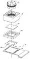
도1은 본 발명의 바람직한 실시예에 따르는 카메라 모듈의 사시도이다.
도2는 본 발명의 전술된 바람직한 실시예에 따르는 카메라 모듈의 분해조립도이다.
도3은 본 발명의 전술된 바람직한 실시예에 따라 압축 몰딩되는 경우의 회로 보드의 사시도이다.1 is a perspective view of a camera module according to a preferred embodiment of the present invention.
2 is an exploded view of the camera module according to the above-described preferred embodiment of the present invention.
3 is a perspective view of a circuit board in the case of compression molding according to the above-described preferred embodiment of the present invention.
이하의 설명은 당업자가 본 발명을 만들고 사용할 수 있도록 개시된다. 바람직한 실시예가 단지 예로서 이하의 설명에 제공되고 변형은 당업자에게 명백할 것이다. 이하의 설명에서 규정되는 일반적인 원리는 본 발명의 사상 및 범주를 벗어나지 않고서 다른 실시, 대안, 변형, 등가물, 및 적용에 적용될 수 있다.The following description is disclosed so that those skilled in the art can make and use the present invention. Preferred embodiments are provided in the following description by way of example only and modifications will be apparent to those skilled in the art. The general principles defined in the following description can be applied to other implementations, alternatives, modifications, equivalents, and applications without departing from the spirit and scope of the invention.
당업자라면 본 발명의 상세한 설명에서, 종방향, 횡방향, 상부, 하부, 전면, 후방, 좌측, 우측, 수직, 수평, 상단, 하단, 내부, 외부 등등으로 사용되는 용어는 단지 도면에 도시된 방향 및 위치 관계에 따르는 방향 관계를 표시하기 위한 것이라는 것을 이해할 것이다. 이것은 단지 설명을 위한 것으로, 디바이스 또는 부품이 특정 방향으로 제조 또는 동작해야 한다는 것을 표시하기 위한 것이 아니며, 따라서 전술된 용어는 본 발명을 제한하는 것이 아니다.For those skilled in the art, in the detailed description of the present invention, terms used in the longitudinal, transverse, upper, lower, front, rear, left, right, vertical, horizontal, top, bottom, inner, outer, etc. directions are only shown in the drawings And it will be understood that it is intended to indicate the directional relationship according to the positional relationship. This is for illustrative purposes only, and is not intended to indicate that a device or component should be manufactured or operated in a particular direction, and therefore the terms described above do not limit the invention.
도1 내지 도3을 살펴보면, 본 발명의 바람직한 실시예에 따르는 카메라 모듈이 예시된다. 카메라 모듈은 프레임(10), 회로 보드(20), 광감성 칩(30)과 같은 광감지 센서, 광학 렌즈(40), 및 모터(50)와 같은 드라이버를 포함한다. 당업자라면 모터(50)가 없이, 카메라 모듈이 고정 초점 카메라 모듈로서 구현될 수 있다는 것을 이해할 수 있다.1 to 3, a camera module according to a preferred embodiment of the present invention is illustrated. The camera module includes a
도면에 도시된 바와 같이, 감광성 칩(300은 회로 보드(20) 상에 제공된다. 프레임(10)은 회로 보드(20) 상에 설치된다. 광학 렌즈(40)는 프레임(10) 상에 장착된 모터(50) 상에 장착된다. 따라서 광학 렌즈(40)는 광학 렌즈(40)를 통해 이동하는 방출 광이 감광성 칩(30)에 의해 감지될 수 있는 방식으로 회로 보드(20) 위에 지지되고 위치한다.As shown in the figure, a photosensitive chip 300 is provided on the
구체적으로, 광학 렌즈(40)는 모터(50) 상에 장착되고, 자동 초점을 위해 모터에 의해 구동될 수 있다. 회로 보드(20) 및 모터(50)는 프레임(10)의 마주보는 면 상에 각각 제공되고, 광학 렌즈(40)가 감광성 칩(30)의 감광 경로를 따라 위치하도록 만든다. 카메라 모듈이 물체의 이미지를 포착하는데 사용되는 경우, 물체의 반사 광은 광학 렌즈에 의해 처리되고 추가로 광전 변환을 위해 감광성 칩(30)에 의해 수용될 수 있다.Specifically, the
회로 보드(20)는 다수의 회로 보드 전도성 부재(21), 회로 보드 본체(22) 및 회로(23)를 포함하는데, 회로 보드 전도성 부재(21)는 광-감지 칩(30)을 전기적으로 연결하기 위해 회로 보드 본체(22) 상에 제공된다. 회로(23)는 회로 보드(22) 상에 제공된다.The
구체적으로, 감광성 칩(30)은 다수의 감광성 칩 전도성 부재 및 감광성 칩 본체를 포함하는데, 감광성 칩 전도성 부재는 감광성 칩 본체 상에 제공된다. 감광성 칩 전도성 부재는 회로 보드(20)와 회로 보드 전도성 부재(21)를 전기적으로 연결하는데 사용되어, 감광성 칩(30)과 회로 보드(20)의 전기 연결을 보장하도록 한다. 구체적으로, 감광성 칩과 회로 보드(20)는 리드선, 또는 납땜, ACP(이방성 전도성 페이스트) 및 고온 압출과 같은 다른 전기 연결 방법에 의해 전기적으로 연결된다. 당업자라면 리드선이 단지 예시적인 것으로 본 발명의 한정하기 위한 것이 아님을 이해할 것이다.Specifically, the
본 발명에 따르면, 회로 보드(20)는 통상적인 회로 보드 제조 방법과 상이한 압출 몰딩에 의해 형성된다는 것을 언급할 가치가 있다. 특히, 회로 보드(20)를 제조하기 위해, 수지의 층은 보강 부재(201) 또는 구리 보드 상에 적층되어 회로 보드 본체(22)를 형성한다. 다시 말해서, 회로 보드(21)는 몰딩에 의해 일체로 형성된다. 몰딩 공정 도중에, 상이한 재료가 몰딩을 위해 사용될 수 있다. 본 발명의 일 실시예에서, 에폭시 수지와 같은 용융 물질 또는 고온 경화성 물질을 사용하는 것이 바람직하다. 당업자라면 에폭시 수지와 같은 용융 물질 또는 고온 경화성 물질은 단지 예시적인 것으로 본 발명의 제한하기 위한 것이 아님을 이해할 수 있을 것이다.According to the present invention, it is worth mentioning that the
더욱 구체적으로, 이 실시예의 압축 몰딩된 회로 보드는 압축 몰딩에 의해 제조된다. 구체적으로, 전기도금 회로 및 필름/수지 필름은 몰딩 다이 안에 첨가된다. 다음으로, 수지 분말 충진 또는 주입 등으로 수지 분말이 채워진다. 그리고 마지막으로 몰딩을 폐쇄하고 눌러서 회로 보드를 형성한다.More specifically, the compression molded circuit board of this embodiment is manufactured by compression molding. Specifically, the electroplating circuit and film/resin film are added into the molding die. Next, the resin powder is filled by filling or injecting the resin powder. And finally, the molding is closed and pressed to form a circuit board.
특히, 본 발명의 바람직한 실시예에 따르면, 도3에 도시된 바와 같이, 보강 부재(201)가 몰딩 다이(도시되지 않음) 안으로 수용된 다음, 전도성 부재(202)가 수지 분말과 같은 수지 물질(203)과 함께 첨가된다. 다음으로, 몰딩 다이는 미리 정해진 온도까지 가열된다. 수지 분말이 열에 의해 용융되어 점성 유체가 되는 경우, 압력의 영향으로, 점성 유체가 흘러서 전체 몰딩 다이의 내부 공동을 채운다. 다음으로, 온도가 연속적으로 증가하는 동안, 수지는 상호결합되고 그 몰(mole) 중량이 증가되어, 점성 유체가 그 유동성을 추가로 잃고 응고된다. 저항, 커패시터 및 드라이버 칩과 같은 전기 및 전자 부품(204)은 추가로 부착되고 전도성 부재와 연결되어 완전한 회로 보드(20)를 형성할 수 있다.In particular, according to a preferred embodiment of the present invention, as shown in FIG. 3, after the reinforcing
수지 물질(203)이 첨가되는 경우, 몰딩 다이 안에 용융된 수지 물질(203)을 주입하는 것이 가능하고, 다음으로 압력 및 열을 가함으로써, 수지 물질(203)이 응고된다는 것이 이해될 것이다. 전도성 부재의 층(202) 및 수지 물질의 층(203)을 반복적으로 중첩되게 추가하여 다층 구조체를 형성하는 것이 가능하다. 전도성 부재(202) 및 전기 부품(204)은 회로 보드(20)의 회로(23)를 형성한다. 전술된 전기 프레임 및 일체형 회로 보드 부재는 유사한 제조 방법을 사용하여 제조될 수 있다.It will be understood that when the
이러한 몰딩 방법에 의해 제조된 회로 보드(21)는 높은 평탄도, 초박형, 고집적도, 미세 선 폭 등과 같은 장점을 갖고, 따라서 회로 부품 구성의 축소 및 회로 보드 크기 증가가 해결될 수 있다는 것을 언급할 가치가 있다. 본 발명의 일 실시예에서, 전술된 바와 같은 압축 몰딩에 의해 제조된 회로 보드 본체(22)는 우수한 평탄성을 갖는다. 배선 폭은 0.1mm 내지 0.09mm 일 수 있다. 회로 보드(20)의 두께는 0.1mm 내지 0.6mm일 수 있다. 회로 보드의 층은 2 내지 10층일 수 있다. 당업자라면 전술된 모든 도면은 단지 예시적인 것으로 한정하기 위한 것은 아님을 이해할 것이다.It should be noted that the
프레임(10)은 필요에 따라 모든 미리정해진 형태로 제조될 수 있다. 다시 말해서, 감광성 칩(30)을 구비한 회로 보드(20)는 통상적인 프레임과 조립될 수 있으며, 프레임(10)은 광학 필터(70)와 함께 추가로 설치될 수 있다.The
또한, 프레임(10)은 전술된 압축 몰딩 기술을 사용하여 제조될 수 있다. 다시 말해서, 회로 보드(20) 및 프레임(10)은 적층된 수지를 일체로 사용하여 제조될 수 있다. 압축 몰딩에서, 감광성 칩(30)을 내부에 장착하기 위해 회로 보드(20)의 상단에 홈(recess)이 제공될 수 있다.Further, the
감광성 칩(30)을 구비한 회로 보드(20)는 고정 초점 카메라 모듈, 자동 초점 카메라 모듈 또는 줌 카메라 모듈과 같은 상이한 종류의 카메라 모듈과 조립될 수 있다. 그리고 연성 PCB를 통해 다양한 전기 디바이스의 제어 패널과 추가로 연결된다. 당업자라면 회로 보드(20)는 예시적인 것일 뿐 본 발명을 제한하기 위한 것이 아님을 이해할 것이다.The
회로 보드(20)의 적용시. 카메라 모듈을 구성하기 위해 단일 회로 보드(20)가 다른 부품과 함께 독립적으로 조립하도록 제조될 수 있다. 다수의 회로 보드20)는 제조방법을 사용하여 제조될 수 있다. 이는 압축 몰딩 공정에 의해 두 피스 이상의 회로 보드(20)로 회로 보드 전체를 형성하고, 다음으로 전체 보드는 다수의 회로 보드(20)로 절단된다. 당업자라면 회로 보드(20)의 수는 예시적인 것일 뿐 본 발명을 제한하기 위한 것이 아님을 이해할 것이다.When the
당업자라면 도면에 도시되고 전술된 본 발명의 실시예는 예시적인 것일 뿐 본 발명을 제한하기 위한 것이 아님을 이해할 것이다.Those skilled in the art will understand that the embodiments of the invention shown in the drawings and described above are illustrative only and are not intended to limit the invention.
따라서 본 발명의 목적은 충분히 효과적으로 달성되었음을 알 수 있을 것이다. 실시예는 본 발명의 기능적이고 구조적인 원리를 예시하기 위해 도시되고 기재되었으며 이러한 윈리를 벗어나지 않고 변경된다. 따라서, 이 발명은 이하의 청구범위의 사상 및 범주내에 포함되는 모든 변형을 포함한다.Therefore, it will be understood that the object of the present invention has been achieved sufficiently effectively. The examples have been shown and described to illustrate the functional and structural principles of the present invention and are modified without departing from this winry. Accordingly, this invention includes all modifications falling within the spirit and scope of the following claims.
10 : 프레임20 : 회로 보드
30 : 감광성 칩40 : 광학 렌즈
50 : 모터10: frame 20: circuit board
30: photosensitive chip 40: optical lens
50: motor
Claims (20)
Translated fromKorean회로 보드 본체 상에 제공되는 회로; 및
감광성 칩을 회로 보드에 전기적으로 연결하기 위해 회로 보드 본체 상에 제공되는 전도성 부재를 포함하는 카메라 모듈의 압축 몰딩된 회로 보드에 있어서,
상기 회로 보드는 보강 부재를 더 포함하고,
상기 회로 보드는, 보강 부재를 몰딩 다이 안에 수용한 후 전도성 부재와 분말상의 수지 물질을 첨가하고, 몰딩 다이를 미리 정해진 온도까지 가열하여 첨가된 분말상 수지 물질을 열에 의해 용융하여 유체상의 점성 유체로 변형시키고, 변형된 점성 유체가 몰딩 다이의 내부의 공동을 충전하고 충전된 유체상의 점성 유체를 응고시킴으로써 형성되는 압출 몰딩에 의해 형성되고,
상기 회로 보드 내의 전도성 부재의 층 및 수지 물질의 층은 반복적으로 중첩되어 이루어진 다층 구조체로 형성된 것을 특징으로 하는
카메라 모듈의 압축 몰딩된 회로 보드.
At least one circuit board body;
A circuit provided on the circuit board body; And
A compression molded circuit board of a camera module comprising a conductive member provided on a circuit board body for electrically connecting a photosensitive chip to the circuit board,
The circuit board further includes a reinforcing member,
The circuit board, after receiving the reinforcing member into the molding die, adds a conductive member and a powdery resin material, heats the molding die to a predetermined temperature, melts the added powdery resin material by heat, and transforms it into a fluid viscous fluid. And the modified viscous fluid is formed by extrusion molding formed by filling the cavity inside the molding die and solidifying the viscous fluid on the filled fluid,
It characterized in that the layer of the conductive member and the layer of the resin material in the circuit board are formed of a multi-layered structure formed by repeatedly overlapping
Compression molded circuit board of the camera module.
상기 회로 보드 본체는 고온 용융 물질 밀 고온 경화성 물질로 구성되는 그룹으로 선택되는 물질로 몰딩되는
카메라 모듈의 압축 몰딩된 회로 보드.
According to claim 1,
The circuit board body is molded of a material selected from the group consisting of a hot melt material mill high temperature curable material
Compression molded circuit board of the camera module.
상기 회로 보드 본체는 고온 용융 물질 또는 고온 경화성 물질을 구비한, 기초(base) 물질로서 상기 보강 부재를 압축 몰딩함으로써 제조되는
카메라 모듈의 압축 몰딩된 회로 보드.
According to claim 1,
The circuit board body is manufactured by compression molding the reinforcing member as a base material with a hot melt material or a hot curable material
Compression molded circuit board of the camera module.
상기 기초 물질은 에폭시 수지인
카메라 모듈의 압축 몰딩된 회로 보드.
According to claim 3,
The base material is an epoxy resin
Compression molded circuit board of the camera module.
상기 회로 보드는 압축 몰딩에 의해 제조된 다수의 회로 보드의 전체를 다수의 상기 회로 보드로 절단함으로써 제조되는
카메라 모듈의 압축 몰딩된 회로 보드.
According to claim 1,
The circuit board is manufactured by cutting the whole of a plurality of circuit boards manufactured by compression molding into a plurality of the circuit boards.
Compression molded circuit board of the camera module.
상기 회로 보드는 압축 몰딩에 의해 제조된 다수의 회로 보드의 전체를 다수의 상기 회로 보드로 절단함으로써 제조되는
카메라 모듈의 압축 몰딩된 회로 보드.
According to claim 4,
The circuit board is manufactured by cutting the whole of a plurality of circuit boards manufactured by compression molding into a plurality of the circuit boards.
Compression molded circuit board of the camera module.
감광성 칩; 및
압축 몰딩에 의해 제조된 압축 몰딩된 회로 보드를 포함하고,
상기 광학 렌즈는 상기 압축 몰딩된 회로 보드와 전기적으로 연결되는 상기 감광성 칩의 감광 경로에 제공되고,
상기 회로 보드는, 적어도 하나의 회로 보드 본체; 회로 보드 본체 상에 제공되는 회로; 및 감광성 칩을 회로 보드에 전기적으로 연결하기 위해 회로 보드 본체 상에 제공되는 전도성 부재를 포함하고,
상기 회로 보드는 보강 부재를 더 포함하고,
상기 회로 보드는, 보강 부재를 몰딩 다이 안에 수용한 후 전도성 부재와 분말상의 수지 물질을 첨가하고, 몰딩 다이를 미리 정해진 온도까지 가열하여 첨가된 분말상 수지 물질을 열에 의해 용융하여 유체상의 점성 유체로 변형시키고, 변형된 점성 유체가 몰딩 다이의 내부의 공동을 충전하고 충전된 유체상의 점성 유체를 응고시킴으로써 형성되는 압출 몰딩에 의해 형성되고,
상기 회로 보드 내의 전도성 부재의 층 및 수지 물질의 층은 반복적으로 중첩되어 다층 구조체로 형성된 것을 특징으로 하는
카메라 모듈.
Optical lenses;
Photosensitive chip; And
A compression molded circuit board manufactured by compression molding,
The optical lens is provided in a photosensitive path of the photosensitive chip electrically connected to the compression molded circuit board,
The circuit board may include at least one circuit board body; A circuit provided on the circuit board body; And a conductive member provided on the circuit board body to electrically connect the photosensitive chip to the circuit board,
The circuit board further includes a reinforcing member,
The circuit board, after receiving the reinforcing member in the molding die, adds a conductive member and a powdery resin material, heats the molding die to a predetermined temperature, melts the added powdery resin material by heat, and transforms it into a fluid viscous fluid. And the modified viscous fluid is formed by extrusion molding formed by filling the cavity inside the molding die and solidifying the viscous fluid on the filled fluid,
The layer of the conductive member and the layer of the resin material in the circuit board are repeatedly overlapped to form a multilayer structure.
Camera module.
상기 카메라 모듈은 고정 초점 카메라 모듈인
카메라 모듈.
The method of claim 7,
The camera module is a fixed focus camera module
Camera module.
드라이버를 추가로 포함하고,
상기 광학 렌즈는 자동 초점 카메라 모듈을 형성하기 위해 상기 드라이버 상에 설치되는
카메라 모듈.
The method of claim 7,
Additional drivers,
The optical lens is installed on the driver to form an autofocus camera module
Camera module.
상기 회로 보드 본체는 고온 용융 물질 및 고온 경화 물질로 구성되는 그룹으로부터 선택되는 물질로 제조되는
카메라 모듈.
The method of claim 7,
The circuit board body is made of a material selected from the group consisting of a hot melt material and a hot hard material
Camera module.
상기 회로 보드 본체는 고온 용융 믈질 및 고온 경화성 물질로 구성되는 그룹으로부터 선택되는 물질을 구비한, 기초(base) 물질로서 상기 보강 부재를 압축 몰딩함으로써 제조되는
카메라 모듈.
The method of claim 7,
The circuit board body is produced by compression molding the reinforcing member as a base material, with a material selected from the group consisting of hot-melt and hot-curable materials.
Camera module.
상기 기초 물질은 에폭시 수지인
카메라 모듈.
The method of claim 12,
The base material is an epoxy resin
Camera module.
상기 회로 보드 상에 설치되는 프레임을 추가로 포함하는
카메라 모듈.
The method of claim 7,
Further comprising a frame installed on the circuit board
Camera module.
상기 프레임 상에 제공되는 광학 필터를 추가로 포함하는
카메라 모듈.
The method of claim 14,
Further comprising an optical filter provided on the frame
Camera module.
(b) 상기 회로 보드에 감광성 칩을 전기적으로 연결하고 상기 감광성 칩의 감광 경로 안에 광학 렌즈를 설치하는 단계를 포함하고,
단계 (a)는
몰딩 다이 내에 보강 부재를 제공하는 단계;
몰딩 다이 내의 보강 부재 위로 전도성 부재와 분말상 수지 물질을 첨가하는 단계;
몰딩 다이를 미리 정해진 온도까지 가열하여 첨가된 분말상 수지 물질을 열에 의해 용융하여 유체상의 점성 유체로 변형시키는 단계;
변형된 점성 유체가 몰딩 다이의 내부의 공동을 충전시키는 단계;
공동을 충전한 점성 유체를 응고시키는 단계;를 포함하는 것을 특징으로 하는
카메라 모듈 제조 방법.
(a) obtaining a circuit board by compression molding; And
(b) electrically connecting a photosensitive chip to the circuit board and installing an optical lens in the photosensitive path of the photosensitive chip,
Step (a)
Providing a reinforcement member within the molding die;
Adding a conductive member and a powdery resin material over the reinforcing member in the molding die;
Heating the molding die to a predetermined temperature to melt the added powdery resin material by heat to transform it into a viscous fluid in the fluid phase;
A modified viscous fluid filling the cavity inside the molding die;
Solidifying the viscous fluid filling the cavity; characterized in that it comprises a
Method of manufacturing a camera module.
단계 (a)는 전도성 부재의 적어도 한 층 및 상기 물질의 적어도 한 층을 압축 몰딩함으로써 하나 이상의 층의 구조체를 구비한 회로 보드를 형성하는 단계를 추가로 포함하는
카메라 모듈 제조 방법.
The method of claim 16,
Step (a) further comprises forming a circuit board having one or more layers of structures by compression molding at least one layer of the conductive member and at least one layer of the material.
Method of manufacturing a camera module.
상기 수지 물질은 에폭시 수지인
카메라 모듈 제조 방법.
The method of claim 16,
The resin material is an epoxy resin
Method of manufacturing a camera module.
단계 (a)는 다수의 회로 보드의 전체 피스를 형성하는 단계 및
다수의 회로 보드의 전체 피스를 압축 몰딩된 회로 보드인 다수의 단일 회로 보드로 절단하는
카메라 모듈 제조 방법.
The method of claim 16,
Step (a) comprises forming the entire piece of a plurality of circuit boards and
Cutting the entire piece of multiple circuit boards into multiple single circuit boards, which are compression molded circuit boards
Method of manufacturing a camera module.
Applications Claiming Priority (4)
| Application Number | Priority Date | Filing Date | Title |
|---|---|---|---|
| CN201610102572.XACN105721749B (en) | 2016-02-24 | 2016-02-24 | Camera module, electric support and circuit board assembly thereof and manufacturing method |
| CN201610102572.X | 2016-02-24 | ||
| US15/057,078 | 2016-02-29 | ||
| US15/057,078US11051400B2 (en) | 2016-02-24 | 2016-02-29 | Camera module with compression-molded circuit board and manufacturing method thereof |
Publications (2)
| Publication Number | Publication Date |
|---|---|
| KR20170099764A KR20170099764A (en) | 2017-09-01 |
| KR102132512B1true KR102132512B1 (en) | 2020-07-09 |
Family
ID=56156964
Family Applications (1)
| Application Number | Title | Priority Date | Filing Date |
|---|---|---|---|
| KR1020170021007AActiveKR102132512B1 (en) | 2016-02-24 | 2017-02-16 | Camera module with compression-molded circuit board and manufacturing method thereof |
Country Status (4)
| Country | Link |
|---|---|
| US (2) | US11051400B2 (en) |
| KR (1) | KR102132512B1 (en) |
| CN (1) | CN105721749B (en) |
| WO (1) | WO2017144005A1 (en) |
Families Citing this family (21)
| Publication number | Priority date | Publication date | Assignee | Title |
|---|---|---|---|---|
| KR102400658B1 (en)* | 2015-07-27 | 2022-05-20 | 엘지이노텍 주식회사 | Camera Module |
| CN105721749B (en)* | 2016-02-24 | 2020-07-24 | 宁波舜宇光电信息有限公司 | Camera module, electric support and circuit board assembly thereof and manufacturing method |
| KR102405359B1 (en)* | 2017-02-08 | 2022-06-07 | 닝보 써니 오포테크 코., 엘티디. | Photographing module and mold photosensitive assembly and manufacturing method thereof, and electronic device |
| CN112600998B (en)* | 2017-07-21 | 2022-06-24 | 宁波舜宇光电信息有限公司 | Camera module, support thereof, photosensitive device, manufacturing method and electronic equipment |
| CN109391750B (en)* | 2017-08-05 | 2023-05-12 | 宁波舜宇光电信息有限公司 | Fixed focus camera module |
| CN109510925A (en)* | 2017-09-15 | 2019-03-22 | 南昌欧菲光电技术有限公司 | Camera module |
| CN109510921B (en)* | 2017-09-15 | 2025-01-10 | 南昌欧菲光电技术有限公司 | Camera module |
| CN109688299B (en)* | 2017-10-18 | 2024-04-09 | 宁波舜宇光电信息有限公司 | Camera module array and corresponding integrated substrate |
| CN109698894B (en)* | 2017-10-20 | 2023-06-30 | 宁波舜宇光电信息有限公司 | Photosensitive assembly and camera module based on metal support |
| CN107734227A (en)* | 2017-10-27 | 2018-02-23 | 昆山丘钛微电子科技有限公司 | Image sensor package structure, camera module and preparation method thereof |
| CN109729242B (en)* | 2017-10-27 | 2020-10-02 | 宁波舜宇光电信息有限公司 | Camera module, expansion wiring packaging photosensitive assembly thereof, jointed board assembly and manufacturing method |
| EP3707750B1 (en)* | 2017-11-07 | 2024-12-04 | AMS Sensors Singapore Pte. Ltd. | Optoelectronic modules having locking assemblies and methods for manufacturing the same |
| CN109917605B (en)* | 2017-12-13 | 2021-06-01 | 三赢科技(深圳)有限公司 | lens module |
| CN110365869A (en)* | 2018-04-11 | 2019-10-22 | 三赢科技(深圳)有限公司 | Camera module and assembly method thereof |
| CN108632514B (en)* | 2018-06-08 | 2024-07-19 | 昆山丘钛微电子科技有限公司 | Camera module and mobile terminal |
| CN110636186B (en)* | 2018-06-22 | 2024-12-31 | 宁波舜宇光电信息有限公司 | Molded photosensitive component and camera module and manufacturing method thereof and electronic device |
| CN109361834A (en)* | 2018-10-15 | 2019-02-19 | 信利光电股份有限公司 | Camera module structure |
| CN109068046B (en)* | 2018-10-17 | 2020-05-15 | 宁波为森智能传感技术有限公司 | Camera module and assembly process |
| TWI793505B (en)* | 2021-01-18 | 2023-02-21 | 新煒科技有限公司 | Camera module and electronic device |
| CN114827389A (en) | 2021-01-18 | 2022-07-29 | 三赢科技(深圳)有限公司 | Camera module and electronic equipment |
| CN113629086A (en)* | 2021-08-03 | 2021-11-09 | 深圳市群晖智能科技股份有限公司 | Manufacturing method of FCM packaging chip machine, packaging chip machine and camera module product |
Citations (2)
| Publication number | Priority date | Publication date | Assignee | Title |
|---|---|---|---|---|
| US20140170797A1 (en)* | 2012-12-17 | 2014-06-19 | Stack Devices Corp. | Sensor chip protective image sensor packaging method |
| US20150062422A1 (en)* | 2013-08-27 | 2015-03-05 | Semiconductor Components Industries, Llc | Lens alignment in camera modules using phase detection pixels |
Family Cites Families (36)
| Publication number | Priority date | Publication date | Assignee | Title |
|---|---|---|---|---|
| US4327126A (en)* | 1980-11-10 | 1982-04-27 | Ralph Ogden | Method of making printed circuit boards |
| DE4003344C1 (en)* | 1990-02-05 | 1991-06-13 | Fa. Carl Freudenberg, 6940 Weinheim, De | |
| US5519177A (en)* | 1993-05-19 | 1996-05-21 | Ibiden Co., Ltd. | Adhesives, adhesive layers for electroless plating and printed circuit boards |
| JP2746171B2 (en)* | 1995-02-21 | 1998-04-28 | 日本電気株式会社 | Solid-state imaging device and manufacturing method thereof |
| MY144573A (en)* | 1998-09-14 | 2011-10-14 | Ibiden Co Ltd | Printed circuit board and method for its production |
| JP3980801B2 (en)* | 1999-09-16 | 2007-09-26 | 株式会社東芝 | Three-dimensional structure and manufacturing method thereof |
| US6570099B1 (en)* | 1999-11-09 | 2003-05-27 | Matsushita Electric Industrial Co., Ltd. | Thermal conductive substrate and the method for manufacturing the same |
| TWI242398B (en)* | 2000-06-14 | 2005-10-21 | Matsushita Electric Industrial Co Ltd | Printed circuit board and method of manufacturing the same |
| US7394663B2 (en)* | 2003-02-18 | 2008-07-01 | Matsushita Electric Industrial Co., Ltd. | Electronic component built-in module and method of manufacturing the same |
| TW200505304A (en)* | 2003-05-20 | 2005-02-01 | Matsushita Electric Industrial Co Ltd | Multilayer circuit board and method for manufacturing the same |
| CN101086546A (en)* | 2006-06-09 | 2007-12-12 | 鸿富锦精密工业(深圳)有限公司 | Lens module and camera module |
| CN101137007A (en)* | 2006-09-01 | 2008-03-05 | 致伸科技股份有限公司 | Camera module and assembling method thereof |
| US20100103296A1 (en)* | 2007-04-13 | 2010-04-29 | Yasushi Nakagiri | Solid-state imaging apparatus and manufacturing method thereof |
| KR100908199B1 (en)* | 2008-07-30 | 2009-07-20 | 주식회사 메카비젼 | Camera module with image sensor chip and manufacturing method |
| US20100025793A1 (en)* | 2008-08-01 | 2010-02-04 | Impac Technology Co., Ltd. | Assembly for image sensing chip and assembling method thereof |
| KR101070058B1 (en)* | 2008-12-24 | 2011-10-04 | 삼성전기주식회사 | Camera Module Package |
| JP2011039462A (en)* | 2009-08-18 | 2011-02-24 | Sony Corp | Lens barrel, camera module, and imaging apparatus |
| ES2405981T3 (en)* | 2009-12-28 | 2013-06-04 | Nagraid S.A. | Procedure for manufacturing electronic cards |
| JP5934109B2 (en)* | 2010-01-11 | 2016-06-15 | フレクストロニクス エイピー エルエルシーFlextronics Ap,Llc | Camera module with molded tape flip chip imaging device mounting and manufacturing method |
| KR101170734B1 (en)* | 2010-07-23 | 2012-08-03 | 엘지이노텍 주식회사 | Camera module |
| JP5541122B2 (en)* | 2010-11-30 | 2014-07-09 | 山一電機株式会社 | Flexible wiring board |
| US20130128106A1 (en)* | 2011-11-23 | 2013-05-23 | Flextronics Ap, Llc | Camera module housing having molded tape substrate with folded leads |
| JP2014007182A (en)* | 2012-06-21 | 2014-01-16 | Fujitsu Ltd | Manufacturing method of laminated circuit board |
| KR102047373B1 (en)* | 2012-07-30 | 2019-11-21 | 엘지이노텍 주식회사 | Camera Module |
| JP5660262B1 (en)* | 2013-03-07 | 2015-01-28 | 株式会社村田製作所 | Camera module and electronic device |
| CN104954637B (en)* | 2014-03-26 | 2018-10-26 | 南昌欧菲光电技术有限公司 | Camera module and manufacturing method thereof |
| CN105262936A (en)* | 2014-07-17 | 2016-01-20 | 宁波舜宇光电信息有限公司 | Manufacturing method of camera module and module semi-finished product thereof |
| TWI576023B (en)* | 2014-10-23 | 2017-03-21 | Elite Material Co Ltd | Suitable for multi-layer printed circuit board design |
| CN104580856A (en)* | 2014-12-25 | 2015-04-29 | 南昌欧菲光电技术有限公司 | Camera module and camera equipment provided with same |
| KR102390760B1 (en)* | 2015-02-13 | 2022-04-26 | 삼성전자주식회사 | Camera device and electronic device therefof |
| US9848111B1 (en)* | 2015-03-17 | 2017-12-19 | Amazon Technologies, Inc. | Imager module with molded packaging |
| KR101949632B1 (en)* | 2015-03-26 | 2019-02-18 | 데쿠세리아루즈 가부시키가이샤 | Method for manufacturing flexible mounting module body |
| CN107771125B (en)* | 2015-06-09 | 2020-07-28 | 罗杰斯公司 | Circuit materials and articles formed therefrom |
| CN105100571A (en)* | 2015-07-28 | 2015-11-25 | 南昌欧菲光电技术有限公司 | Camera module group and first and second circuit boards thereof |
| CN105100569A (en)* | 2015-07-28 | 2015-11-25 | 南昌欧菲光电技术有限公司 | Camera module and its first circuit board and second circuit board |
| CN105721749B (en)* | 2016-02-24 | 2020-07-24 | 宁波舜宇光电信息有限公司 | Camera module, electric support and circuit board assembly thereof and manufacturing method |
- 2016
- 2016-02-24CNCN201610102572.XApatent/CN105721749B/enactiveActive
- 2016-02-29USUS15/057,078patent/US11051400B2/enactiveActive
- 2017
- 2017-02-16KRKR1020170021007Apatent/KR102132512B1/enactiveActive
- 2017-02-24WOPCT/CN2017/074699patent/WO2017144005A1/ennot_activeCeased
- 2021
- 2021-05-18USUS17/323,079patent/US20220304148A9/ennot_activeAbandoned
Patent Citations (2)
| Publication number | Priority date | Publication date | Assignee | Title |
|---|---|---|---|---|
| US20140170797A1 (en)* | 2012-12-17 | 2014-06-19 | Stack Devices Corp. | Sensor chip protective image sensor packaging method |
| US20150062422A1 (en)* | 2013-08-27 | 2015-03-05 | Semiconductor Components Industries, Llc | Lens alignment in camera modules using phase detection pixels |
Also Published As
| Publication number | Publication date |
|---|---|
| US20210329781A1 (en) | 2021-10-21 |
| CN105721749B (en) | 2020-07-24 |
| KR20170099764A (en) | 2017-09-01 |
| CN105721749A (en) | 2016-06-29 |
| US11051400B2 (en) | 2021-06-29 |
| WO2017144005A1 (en) | 2017-08-31 |
| US20220304148A9 (en) | 2022-09-22 |
| US20170245363A1 (en) | 2017-08-24 |
Similar Documents
| Publication | Publication Date | Title |
|---|---|---|
| KR102132512B1 (en) | Camera module with compression-molded circuit board and manufacturing method thereof | |
| US11706516B2 (en) | Camera module and array camera module with circuit board unit and photosensitive unit and manufacturing method thereof | |
| JP7059181B2 (en) | Multi-lens camera module coupling stand, multi-lens camera module, and its use | |
| CN206272706U (en) | Array camera module and dual camera module, circuit board assembly and electronic equipment thereof | |
| CN206212112U (en) | Array camera module and photosensitive assembly thereof | |
| US10192914B2 (en) | Camera module and array camera module with circuit board unit and photosensitive unit and manufacturing method thereof | |
| TWI657306B (en) | Array camera module and molded photosensitive component thereof, circuit board assembly and manufacturing method, and electronic device | |
| WO2017140118A1 (en) | Array camera module, molded photosensitive component and circuit board component of same, manufacturing method therefor, and electronic device | |
| CN105681637A (en) | Array camera module and photosensitive assembly thereof and manufacturing method | |
| CN112714239B (en) | Photosensitive assembly, camera module, method thereof and electronic equipment | |
| CN109585464B (en) | Camera module, photosensitive component and manufacturing method thereof | |
| CN114710609A (en) | Autofocus camera module and autofocus camera module assembly method |
Legal Events
| Date | Code | Title | Description |
|---|---|---|---|
| PA0109 | Patent application | Patent event code:PA01091R01D Comment text:Patent Application Patent event date:20170216 | |
| PG1501 | Laying open of application | ||
| A201 | Request for examination | ||
| PA0201 | Request for examination | Patent event code:PA02012R01D Patent event date:20180425 Comment text:Request for Examination of Application Patent event code:PA02011R01I Patent event date:20170216 Comment text:Patent Application | |
| E902 | Notification of reason for refusal | ||
| PE0902 | Notice of grounds for rejection | Comment text:Notification of reason for refusal Patent event date:20190924 Patent event code:PE09021S01D | |
| E701 | Decision to grant or registration of patent right | ||
| PE0701 | Decision of registration | Patent event code:PE07011S01D Comment text:Decision to Grant Registration Patent event date:20200419 | |
| PR0701 | Registration of establishment | Comment text:Registration of Establishment Patent event date:20200703 Patent event code:PR07011E01D | |
| PR1002 | Payment of registration fee | Payment date:20200703 End annual number:3 Start annual number:1 | |
| PG1601 | Publication of registration | ||
| PR1001 | Payment of annual fee | Payment date:20240522 Start annual number:5 End annual number:5 |