KR102125887B1 - Led lamp - Google Patents
Led lampDownload PDFInfo
- Publication number
- KR102125887B1 KR102125887B1KR1020137016970AKR20137016970AKR102125887B1KR 102125887 B1KR102125887 B1KR 102125887B1KR 1020137016970 AKR1020137016970 AKR 1020137016970AKR 20137016970 AKR20137016970 AKR 20137016970AKR 102125887 B1KR102125887 B1KR 102125887B1
- Authority
- KR
- South Korea
- Prior art keywords
- light
- light emitting
- emitting device
- envelope
- delete delete
- Prior art date
- Legal status (The legal status is an assumption and is not a legal conclusion. Google has not performed a legal analysis and makes no representation as to the accuracy of the status listed.)
- Active
Links
Images


Classifications
- F—MECHANICAL ENGINEERING; LIGHTING; HEATING; WEAPONS; BLASTING
- F21—LIGHTING
- F21V—FUNCTIONAL FEATURES OR DETAILS OF LIGHTING DEVICES OR SYSTEMS THEREOF; STRUCTURAL COMBINATIONS OF LIGHTING DEVICES WITH OTHER ARTICLES, NOT OTHERWISE PROVIDED FOR
- F21V3/00—Globes; Bowls; Cover glasses
- F21V3/04—Globes; Bowls; Cover glasses characterised by materials, surface treatments or coatings
- F—MECHANICAL ENGINEERING; LIGHTING; HEATING; WEAPONS; BLASTING
- F21—LIGHTING
- F21K—NON-ELECTRIC LIGHT SOURCES USING LUMINESCENCE; LIGHT SOURCES USING ELECTROCHEMILUMINESCENCE; LIGHT SOURCES USING CHARGES OF COMBUSTIBLE MATERIAL; LIGHT SOURCES USING SEMICONDUCTOR DEVICES AS LIGHT-GENERATING ELEMENTS; LIGHT SOURCES NOT OTHERWISE PROVIDED FOR
- F21K9/00—Light sources using semiconductor devices as light-generating elements, e.g. using light-emitting diodes [LED] or lasers
- F21K9/20—Light sources comprising attachment means
- F21K9/23—Retrofit light sources for lighting devices with a single fitting for each light source, e.g. for substitution of incandescent lamps with bayonet or threaded fittings
- F21K9/232—Retrofit light sources for lighting devices with a single fitting for each light source, e.g. for substitution of incandescent lamps with bayonet or threaded fittings specially adapted for generating an essentially omnidirectional light distribution, e.g. with a glass bulb
- F—MECHANICAL ENGINEERING; LIGHTING; HEATING; WEAPONS; BLASTING
- F21—LIGHTING
- F21K—NON-ELECTRIC LIGHT SOURCES USING LUMINESCENCE; LIGHT SOURCES USING ELECTROCHEMILUMINESCENCE; LIGHT SOURCES USING CHARGES OF COMBUSTIBLE MATERIAL; LIGHT SOURCES USING SEMICONDUCTOR DEVICES AS LIGHT-GENERATING ELEMENTS; LIGHT SOURCES NOT OTHERWISE PROVIDED FOR
- F21K9/00—Light sources using semiconductor devices as light-generating elements, e.g. using light-emitting diodes [LED] or lasers
- F21K9/60—Optical arrangements integrated in the light source, e.g. for improving the colour rendering index or the light extraction
- F—MECHANICAL ENGINEERING; LIGHTING; HEATING; WEAPONS; BLASTING
- F21—LIGHTING
- F21V—FUNCTIONAL FEATURES OR DETAILS OF LIGHTING DEVICES OR SYSTEMS THEREOF; STRUCTURAL COMBINATIONS OF LIGHTING DEVICES WITH OTHER ARTICLES, NOT OTHERWISE PROVIDED FOR
- F21V29/00—Protecting lighting devices from thermal damage; Cooling or heating arrangements specially adapted for lighting devices or systems
- F21V29/50—Cooling arrangements
- F21V29/70—Cooling arrangements characterised by passive heat-dissipating elements, e.g. heat-sinks
- F21V29/74—Cooling arrangements characterised by passive heat-dissipating elements, e.g. heat-sinks with fins or blades
- F21V29/77—Cooling arrangements characterised by passive heat-dissipating elements, e.g. heat-sinks with fins or blades with essentially identical diverging planar fins or blades, e.g. with fan-like or star-like cross-section
- F21V29/773—Cooling arrangements characterised by passive heat-dissipating elements, e.g. heat-sinks with fins or blades with essentially identical diverging planar fins or blades, e.g. with fan-like or star-like cross-section the planes containing the fins or blades having the direction of the light emitting axis
- F—MECHANICAL ENGINEERING; LIGHTING; HEATING; WEAPONS; BLASTING
- F21—LIGHTING
- F21Y—INDEXING SCHEME ASSOCIATED WITH SUBCLASSES F21K, F21L, F21S and F21V, RELATING TO THE FORM OR THE KIND OF THE LIGHT SOURCES OR OF THE COLOUR OF THE LIGHT EMITTED
- F21Y2115/00—Light-generating elements of semiconductor light sources
- F21Y2115/10—Light-emitting diodes [LED]
Landscapes
- Engineering & Computer Science (AREA)
- General Engineering & Computer Science (AREA)
- Physics & Mathematics (AREA)
- Microelectronics & Electronic Packaging (AREA)
- Optics & Photonics (AREA)
- Non-Portable Lighting Devices Or Systems Thereof (AREA)
- Led Device Packages (AREA)
- Arrangement Of Elements, Cooling, Sealing, Or The Like Of Lighting Devices (AREA)
- Arrangements Of Lighting Devices For Vehicle Interiors, Mounting And Supporting Thereof, Circuits Therefore (AREA)
Abstract
Translated fromKoreanDescription
Translated fromKorean본 발명은 조명 기술, 발광 기술, 고체(solid-state) 발광 기술 및 관련 기술에 관한 것이다.The present invention relates to lighting technology, light emission technology, solid-state light emission technology and related technologies.
종래에, 백열 램프 및 할로겐 램프는 전방향(omnidirectional) 및 지향성 광원 양자로서 사용된다. 전방향 램프는, 램프로부터 1미터 이상 멀리 떨어진 원거리에서 실질적으로 균일한 강도 분포 대 각도를 제공하고, 데스크 램프, 테이블 램프, 장식 램프, 샹들리에, 천장 고정구, 및 전방향에서 광의 균일한 분포가 바람직한 다른 분야에서와 같이 다양한 응용분야에서 사용할 수 있게 하는 것이다.Conventionally, incandescent lamps and halogen lamps are used as both omnidirectional and directional light sources. The omni-directional lamp provides a substantially uniform intensity distribution versus angle at a distance of at least 1 meter away from the lamp, and a uniform distribution of light in the desk lamp, table lamp, decorative lamp, chandelier, ceiling fixture, and omnidirectional is desirable It is intended to be used in various applications as in other fields.
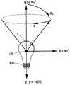
도 1을 참조하면, 도시된 좌표계는 백열 램프, 또는 보다 일반적으로 전방향 조명을 생성하도록 의도되는 모든 램프에 의해 생성된 조명의 공간적 분포를 설명하기 위해서 본 명세서에서 사용한다. 좌표계는 구형 좌표계 타입이며, 백열 A-19 스타일 램프(L)를 참조하여 도시되어 있다. 원거리 조명 분포를 설명하기 위해서, 램프(L)는 예를 들면 백열 필라멘트의 위치와 일치할 수 있는 점(L0)에 위치되는 것으로 고려될 수 있다. 지리 분야에서 종래에 이용되던 공간 좌표 표기법을 채택하면, 조명 방향은 고도(elevation) 또는 위도 좌표 및 방위(azimuth) 또는 경도 좌표에 의해 표시될 수 있다. 그러나, 지리 분야 협약에서의 자차(deviation)에서, 본 명세서에서 사용된 고도 또는 위도 좌표는 범위[0°, 180°]를 이용하며, 여기에서 θ=0°은 "지리적 북쪽(geographic north)" 또는 "N"에 대응한다. 이것은 전방향 광에 대응하도록 방향 θ=0°을 따라 조명이 이뤄지기 때문에 편리하다. 북쪽 방향, 즉 방향 θ=0°은 또한 본 명세서에 있어서 광축이라고 한다. 이 표기법을 이용하면, θ=180°은 "지리적 남쪽(geographic south)" 또는 "S"에, 또는 조명 환경에서 역방향 광에 대응한다. 고도 또는 위도 θ=90°은 "지리적 적도(geographic equator)" 또는 조명 환경에서 측방향 광에 대응한다. 정확하게 북쪽 또는 남쪽에서, 즉 θ=0° 또는 θ=180°에서(즉, 광축을 따라서), 방위 또는 경도 좌표는 의미가 없으며, 또는 아마도 보다 정확하게는 퇴보된 것으로 고려될 수 있다는 것을 이해할 수 있다. 다른 "스페셜(special)" 좌표는, 광원을 포함하는(또는 보다 정확하게 원거리 계산을 위한 광원의 공칭 위치, 예를 들면 점(L0)을 포함하는) 광축에 횡단하는 평면을 형성하는 θ=90°이다.Referring to FIG. 1, the illustrated coordinate system is used herein to describe the spatial distribution of illumination generated by incandescent lamps, or more generally all lamps intended to produce omni-directional illumination. The coordinate system is a spherical coordinate system type and is illustrated with reference to the incandescent A-19 style lamp L. To account for the distant illumination distribution, the lamp L can be considered to be located at a point L0, which can for example coincide with the position of the incandescent filament. When spatial coordinate notation, which has been conventionally used in the geography field, is adopted, the lighting direction may be displayed by elevation or latitude coordinates and azimuth or longitude coordinates. However, in the deviation from the geographic field agreement, the altitude or latitude coordinates used herein use a range [0°, 180°], where θ=0° is “geographic north” Or "N". This is convenient because the illumination is made along the direction θ=0° to correspond to the omni-directional light. The north direction, ie direction θ=0°, is also referred to herein as the optical axis. Using this notation, θ=180° corresponds to “geographic south” or “S”, or reverse light in an illumination environment. Elevation or latitude θ=90° corresponds to a “geographic equator” or lateral light in a lighting environment. It can be understood that precisely in the north or south, ie θ=0° or θ=180° (ie, along the optical axis), the orientation or longitude coordinates are meaningless, or perhaps more accurately considered degenerate. . Other “special” coordinates are θ=90° forming a plane transverse to the optical axis that includes the light source (or more accurately includes the nominal position of the light source for distance calculation, for example including the point L0). to be.
실제로, 전체 종방향 폭(span) θ=[0°, 360°]에 교차하는 균일한 광 강도를 성취하는 것은 통상적으로 어렵지 않은데, 그 이유는 균일한 광 강도는 광축을 중심으로(즉, 축 θ=0°을 중심으로) 회전 대칭인 광원을 구성하도록 직선방향이기 때문이다. 예를 들면, 백열 램프(L)는 실질적으로 전방향 광을 발광하도록 설계될 수 있는 좌표 중심(L0)에 위치된 백열 필라멘트를 적절하게 이용하며, 그에 따라 임의의 위도를 위한 방위(θ)에 대해서 균일한 강도 분포를 제공한다.In practice, it is usually not difficult to achieve a uniform light intensity crossing the entire longitudinal span θ=[0°, 360°] because the uniform light intensity is centered around the optical axis (ie, the axis This is because it is linear in order to construct a light source that is rotationally symmetrical around θ=0°. For example, the incandescent lamp L suitably utilizes an incandescent filament located at a coordinate center L0 that can be designed to emit substantially omni-directional light, and accordingly to an orientation θ for any latitude. Provides a uniform intensity distribution.
그러나, 고도 또는 위도 좌표에 대해서 이상적인 전방향 강도를 성취하는 것은 일반적으로 실용적이지 못하다. 예를 들면, 램프(L)는 표준 "에디슨 베이스(Edison base)" 램프 고정구 내에 끼워맞춰지도록 구성되며, 이 단부를 향해서, 백열 램프(L)는 예를 들면 E25, E26 또는 E27 램프 베이스일 수 있는 나사형 에디슨 베이스(EB)를 포함하며, 여기에서 숫자는 베이스(EB)에서 나사 턴(screw turn)의 외경을 가리킨다. 에디슨 베이스(EB)(또는 보다 일반적으로 광원 "뒤쪽(behind)"에 위치되는 모든 전력 입력 시스템)는 광원 위치(L0) "뒤쪽(behind)"에서 광축상에 놓이게 되며, 그에 따라 역방향 발광을 차단하며(즉, 남쪽 위도를 따라, 즉 θ=180°를 따르는 조명을 차단함), 그 결과 백열 램프(L)는 위도 좌표에 대한 이상적인 전방향 광을 제공할 수 없다.However, achieving ideal omnidirectional strength for altitude or latitude coordinates is generally not practical. For example, the lamp L is configured to fit within a standard "Edison base" lamp fixture, and towards this end, the incandescent lamp L can be for example an E25, E26 or E27 lamp base. Includes a threaded Edison base (EB), where the number indicates the outer diameter of the screw turn in the base (EB). The Edison Base (EB) (or more generally any power input system located at the light source “behind”) is placed on the optical axis at the light source location (L0) “behind”, thereby blocking reverse light emission. (I.e., blocking the light along the southern latitude, i.e. θ=180°), and as a result, the incandescent lamp L cannot provide the ideal omnidirectional light for latitude coordinates.
60W Soft White 백열 램프(미국 뉴욕주에 소재하는 제너럴 일렉트릭의 제품)와 같은 시중의 백열 램프는 위도 폭(span) θ=[0°, 135°]에 교차하는 강도를 제공하는 것으로 쉽게 구성되며, 상기 위도 폭(span) θ=[0°, 135°]는 위도 범위에 걸쳐서 평균 강도의 ±20% 내에서 균일하다.Commercially available incandescent lamps, such as 60W Soft White incandescent lamps (products of General Electric, New York, USA), are easily constructed by providing an intensity that crosses the latitude span θ=[0°, 135°], The latitude span θ=[0°, 135°] is uniform within ±20% of the average intensity over the latitude range.
백열 램프 및 할로겐 램프와 비교하여, 발광 다이오드(LED) 장치와 같은 중실형 발광 기술은 본래 매우 지향성인데, 그 이유는 이들 장치는 단지 하나의 측면으로부터만 나오는 평판 장치이기 때문이다. 예를 들면, 봉입체(encapsulation)를 구비하거나 구비하지 않은 LED 장치는, 범위 θ=[0°, 95°]에서 cos(θ)로 변화되는 강도를 갖는 지향성 랑베르(Lambertian) 공간 강도 분포로 발광하며, θ>90°에 대해서 제로 강도를 갖는다. 반도체 레이저는 본래 보다 더 지향성이며, 또한 기본적으로 θ=0° 주변에서 좁은 원뿔로 제한된 전방향 광의 비임으로서 설명할 수 있는 분포를 발광한다.Compared to incandescent lamps and halogen lamps, solid-state light-emitting technologies such as light-emitting diode (LED) devices are inherently highly directional, because these devices are flat panel devices that come only from one side. For example, an LED device with or without encapsulation emits light with a directional Lambertian spatial intensity distribution with intensity varying from cos(θ) in the range θ=[0°, 95°]. , θ>90°. Semiconductor lasers are more directional than they are originally and also emit a distribution that can be described as a beam of omni-directional light limited to a narrow cone basically around θ=0°.
중실형 조명과 관련된 다른 도전으로서, 백열 필라멘트와 달리, LED 칩 또는 다른 중실형 조명 장치는 통상적으로 표준 110V 또는 220V 교류 전력을 이용하여 효율적으로 작동될 수 없다는 것이다. 오히려, 탑재형 전자기기는 통상적으로 교류 입력 전력을 LED 칩을 구동하기 위해서 수정 가능한 낮은 전압의 직류 전압으로 변환하도록 제공된다. 변형예로서, 충분한 개수의 LED 칩의 일련의 스트링은 110V 또는 220V에서 직접 작동될 수 있고, 적당한 극성 제어(예를 들면 제너 다이오드(Zener diodes))와 이러한 스트링의 평행한 배열은 비록 실질적으로 감소된 전력 효율일지라도 110V 또는 220V 교류 전력에서 작동될 수 있다. 양자의 경우에, 전자기기는 일체식 백열 램프 또는 할로겐 램프에 사용된 단순한 에디슨 베이스와 비교할 때 램프 베이스의 추가적인 구성요소를 구성한다. 전자기기에 의해 차지하는 공간은 추가의 광투과 장애물을 형성한다.As another challenge associated with solid-state lighting, unlike incandescent filaments, LED chips or other solid-state lighting devices typically cannot be efficiently operated using standard 110V or 220V AC power. Rather, mounted electronics are typically provided to convert AC input power to a low voltage, DC voltage that can be modified to drive the LED chip. As a variant, a series of strings of a sufficient number of LED chips can be operated directly at 110V or 220V, with proper polarity control (eg Zener diodes) and the parallel arrangement of these strings, although substantially reduced. Even the power efficiency can be operated at 110V or 220V AC power. In both cases, the electronics constitute an additional component of the lamp base as compared to the simple Edison base used for integral incandescent or halogen lamps. The space occupied by the electronics forms additional light-transmitting obstacles.
중실형 조명에서의 또 다른 도전은 히트 싱킹(heat sinking)의 필요성이다. LED 장치는 백열 필라멘트 또는 할로겐 필라멘트와 비교할 때 성능 및 신뢰성 양자에 있어서 온도에 매우 민감하다. 이것은 다량의 히트 싱킹 재료(즉, 히트 싱크)를 LED 장치와의 접촉 또는 달리 LED 장치와 양호한 열적 접촉으로 위치시킴으로써 해결된다. 히트 싱크에 의해 차지한 공간은 방출된 광을 차단하고, 그에 따라 전방향 LED-기반 램프를 형성하는 능력을 추가로 제한한다. 이러한 제한은, LED 램프가 광원, 전자기기, 광학 요소 및 열적 관리를 포함한 모든 램프 구성요소를 위한 최대 치수를 한정하는 전류 규제 제한(ANSI, NEMA 등등)의 물리적인 사이즈로 억제될 때 개선된다.Another challenge in solid-state lighting is the need for heat sinking. LED devices are very sensitive to temperature in both performance and reliability when compared to incandescent or halogen filaments. This is solved by placing a large amount of heat sinking material (ie heat sink) in contact with the LED device or otherwise good thermal contact with the LED device. The space occupied by the heat sinks further blocks the emitted light, thereby further limiting the ability to form omni-directional LED-based lamps. This limitation is improved when the LED lamp is restrained to the physical size of the current regulation limits (ANSI, NEMA, etc.) limiting the maximum dimensions for all lamp components including light sources, electronics, optical elements and thermal management.
전자기기 및 히트 싱킹의 조합은 LED 장치를 L0 위치에 위치시키는 것을 곤란하게 만든다. 따라서, 백열 교체용으로 의도되는 대부분의 시중에서 입수 가능한 LED 램프는 백열 램프와 유사한 균일한 강도 분포를 제공하지 못한다. 더욱이, 광 강도 분포는 적도 아래로 방출되는 광이 거의 없는 상태로 주로 상향으로 지향된다. 이것은 백열 램프를 만족스럽게 모방하는 강도 분포를 제공하지 못한다.The combination of electronics and heat sinking makes it difficult to place the LED device in the L0 position. Thus, most commercially available LED lamps intended for incandescent replacement do not provide a uniform intensity distribution similar to incandescent lamps. Moreover, the light intensity distribution is mainly directed upwards with little light emitted below the equator. This does not provide an intensity distribution that satisfactorily mimics an incandescent lamp.
본 발명은 발광 장치 및 램프를 제공하는 것이다.The present invention provides a light emitting device and a lamp.
본 발명의 제 1 실시형태에 따르면, 광투과 엔벨로프(envelope)를 포함하는 발광 장치가 제공된다. 발광 다이오드 광원은 광투과 엔벨로프의 내부를 조명한다. 박막은 광투과 엔벨로프를 나눈다. 박막은 굴절성이면서 반사성이다.According to the first embodiment of the present invention, a light emitting device including a light transmission envelope is provided. The light emitting diode light source illuminates the interior of the light transmitting envelope. The thin film divides the light transmission envelope. The thin film is refractive and reflective.
본 발명의 제 2 실시형태에 따르면, 복수의 발광 다이오드를 구비하는 광 엔진을 포함하는 램프가 제공된다. 램프는 교류를 직류로 변환하도록 조절된 LED 구동 전자기기를 수용하는 베이스를 더 포함한다. 베이스의 제 1 측부상에는 전기 커넥터가 배치되며, 베이스의 제 2 측부상에는 광투과 본체가 배치된다. 광 엔진에 의해 발광된 광은 광투과 본체에 입사된다. 광투과 본체는 램프의 광축에 실질적으로 수직으로 연장되는 박막 층을 더 포함한다. 박막 층은 굴절성이면서 반사성이다.According to a second embodiment of the present invention, a lamp comprising a light engine having a plurality of light emitting diodes is provided. The lamp further includes a base that accommodates the LED-driven electronics adjusted to convert AC to DC. An electrical connector is disposed on the first side of the base, and a light transmitting body is disposed on the second side of the base. The light emitted by the light engine is incident on the light transmitting body. The light transmitting body further comprises a thin film layer extending substantially perpendicular to the optical axis of the lamp. The thin film layer is refractive and reflective.
본 발명의 제 3 실시형태에 따르면, 교류를 직류로 변환하도록 조절된 LED 구동 전자기기를 갖는 베이스와 조합되는 광투과 엔벨로프를 포함하는 램프가 제공된다. LED 광원은 광투과 엔벨로프의 내부를 조명한다. 박막은 광투과 엔벨로프의 표면상에 배치된다. 박막은 굴절성이면서 반사성이다. 나사, 웨지 또는 포스트 커넥터 중 하나가 또한 마련된다.According to a third embodiment of the present invention, there is provided a lamp comprising a light transmitting envelope in combination with a base having LED driven electronics adjusted to convert alternating current into direct current. The LED light source illuminates the interior of the light transmitting envelope. The thin film is placed on the surface of the light transmitting envelope. The thin film is refractive and reflective. One of the screws, wedges or post connectors is also provided.
도 1은 종래의 백열광 전구를 참조하여, 조명 분포를 설명하기 위해서 본원에서 사용되는 좌표계를 개략적으로 도시하는 도면이다.
도 2는 본 발명의 전방향(omnidirectional) LED-기반 램프를 단면으로 개략적으로 도시하는 도면이다.
도 3은 대안적인 전방향 LED-기반 램프의 측면도이다.
도 4는 대안적인 전방향 LED-기반 램프의 측면도이다.
도 5는 대안적인 전방향 LED-기반 램프의 측면도이다.
도 6은 대안적인 전방향 LED-기반 램프의 측면도이다.
도 7은 히트 싱킹 핀을 포함하는 본 발명의 전방향 LED-기반 램프 실시예를 도시하는 도면이다.1 is a view schematically showing a coordinate system used herein to describe the distribution of illumination with reference to a conventional incandescent light bulb.
2 is a schematic view showing in cross section the omnidirectional LED-based lamp of the present invention.
3 is a side view of an alternative omni-directional LED-based lamp.
4 is a side view of an alternative omni-directional LED-based lamp.
5 is a side view of an alternative omni-directional LED-based lamp.
6 is a side view of an alternative omni-directional LED-based lamp.
7 is a view showing an omni-directional LED-based lamp embodiment of the present invention including a heat sinking pin.
본 발명은 다양한 구성요소 및 구성요소의 배치로 그리고 다양한 프로세스 작동 및 프로세스 작동의 배치로 이뤄진다. 도면은 단지 실시예를 설명하기 위한 것이며, 본 발명을 제한하는 것으로 해석되지 않아야 한다.The invention consists of various components and arrangements of components and various process operations and arrangements of process operations. The drawings are for illustrative purposes only and should not be construed as limiting the invention.
본 실시예는 일체형 교체 LED 램프에 관한 것이며, 램프로의 입력은 메인 전기 공급원이며, 출력은 바람직하게 램프 외부로의 부수적인 전자 또는 광적 성분이 없는 소망의 강도 패턴이다.This embodiment relates to an integral replacement LED lamp, the input to the lamp being the main electrical source, and the output is preferably a desired intensity pattern free of incidental electrons or optical components outside the lamp.
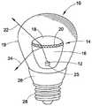
도 2를 참조하면, LED-기반 램프(10)는 LED-기반 광원(12) 및 광투과 엔벨로프(14)를 포함한다. 도시된 광투과 엔벨로프(14)는 광원(12)에 인접하여 배치된 제 1 렌즈 부분(16)과, 먼 렌즈 부분(18)으로 구성된다. 박막(20)은 제 1 렌즈 부분(16)과 먼 렌즈 부분(18) 사이에 배치된다. 또한, 램프(10)는 먼 렌즈 부분(18)을 갖지 않고 구성될 수 있다는 것은 또한 명백하다. 광투과 엔벨로프(14)는 종래의 백열 램프의 형상을 제공하는 유리 전구(19) 내에 포함될 수 있다.Referring to Figure 2, the LED-based
박막(20)은 굴절 광(22) 및 반사된 광(24) 양자 투과를 제공하는 재료 및 두께로부터 선택된다. 박막이 형성되는 예시적인 재료는 알루미늄, 은 및 금을 포함한다. 약 30미크론 및 약 90미크론 사이의 두께를 갖는 박막은 소망의 조합의 반사 및 투과를 제공할 것으로 판단된다. 이러한 방법을 이용함으로써, 광 강도 분포는 맞춰질 수 있다. 또한, 반사된 광은 실질적으로 전방향 광 분포를 생성하도록 사용될 수 있는 반면에, 굴절 광은 백열 램프와 연관된 확산 스파클 효과(diffuse sparkle effect)를 제공한다. 바람직하게, 필름 두께 제어에 의해서, 광 강도 분포는 렌즈 디자인을 변경시킴이 없이 조정될 수 있다.The
특정 실시예에 있어서, 엔벨로프(14)는 유리로 구성되지만, 플라스틱 또는 세라믹과 같은 다른 광투과 재료가 또한 이용될 수 있다. 선택적으로, 엔벨로프(14)는, LED로부터의 광을 다른 칼라로 변환하기 위해, 예를 들면 LED로부터의 청색 또는 자외선(UV) 광을 백색 광으로 변환하기 위해서, 예를 들면 엔벨로프 표면상에 코팅되고 이 표면 전체에 분산된 하나 또는 그 이상의 형광체를 또한 포함할 수 있다. 선택적으로, 형광체는 LED 패키지와 관련이 있을 수 있다. 다른 변형예는 전구(19)상에 또는 전구(19)내에 분산 형광체를 포함한다.In certain embodiments, the
LED-기반 광원(12)은 적어도 하나의 발광 다이오드(LED)를 포함한다. LED로 구성된 광 엔진은 형광체 기반 시스템일 수 있으며, 이 시스템에서 LED 광은 형광체 또는 칼라 혼합 시스템을 여자시키도록 혼합되며, 혼합 시스템에서 상이한 칼라 LED는 소망의 가시광선 출력을 생성하도록 혼합된다. 예를 들면, 몇몇 실시예에 있어서, 제 1 LED 장치는 녹색을 띤 연색 광(예를 들면 적당한 "백색" 형광체로 코팅된 청색 또는 자외선 발광 LED 칩을 이용함으로써 성취될 수 있음)을 출력할 수 있으며, 제 2 LED 장치는 적색 광(예를 들면 적색 광을 본래 발광하는 GaAsP 또는 AlGaInP 또는 다른 에피택시 LED 칩을 이용함으로써 성취될 수 있음)을 출력할 수 있으며, 제 1 및 제 2 LED 장치로부터의 광은 함께 혼합되어 개선된 백색 연색을 생성한다. 한편, LED-기반 광원은 백색 LED 장치 또는 포화색 LED 장치 등일 수 있는 단일 LED 장치를 포함하도록 고려된다. 또한, 레이저 LED 장치는 램프에 합체되도록 고려된다.The LED-based
엔벨로프(14)는 중공형 또는 중실형일 수 있다. 일 실시예에서, 광투과 엔벨로프(14)는 LED-기반 광원(12)을 수용하거나 광원(12)과 합치되는 크기로 된 개구부(25)를 포함하며, 그 결과 LED-기반 광원(12)의 광투과 주요 표면은 엔벨로프(14)의 내부로 향하며, 엔벨로프(14)의 내부로 광을 발광한다.The
LED-기반 광원(12)은 히트 싱킹을 제공하는 베이스(26)에 그리고 교류를 직류로 변환하는 전자기기를 수용하기 위한 공간에 장착된다. 특히, 베이스 요소(26)는 램프(10)를 전력 콘센트에 고정하기 위한 커넥터(28)를 더 포함한다. 에디슨 나사 베이스가 본 도면에 도시되어 있지만, 웨지 또는 포스트 커넥터와 같은 본 기술 분야에 공지된 모든 형태의 커넥터가 적당하다. LED는 선택적으로 금속 코어 인쇄 회로 기판(metal core printed circuit board : MCPCB)인 회로 기판상에 평면 배향으로 장착될 수 있다. 베이스 요소(26)는 LED 장치용 지지부를 제공하며, 열전도성(히트 싱킹)이다.The LED-based
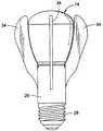
이제, 도 3을 참조하면, 렌즈(16) 및 렌즈(18)의 높이를 변화시키는 개념이 시각적으로 도시되어 있다. 또한, 바닥 길이와 상부 길이 사이의 비율이 변화된다. 렌즈(16)의 표면적은 렌즈(18)의 표면적보다 큰 것이 바람직한데, 아마도 전체 광투과 엔벨로프의 >65%, 바람직하게는 >75%를 구성하는 것이 바람직한 것으로 일반적으로 알려져 있다. 그러나, 본 실시예의 광 분포를 변경하기 위한 가장 효율적인 방법론은 박막의 두께를 변경하는 것으로 알려져 있다. 더욱이, 박막 두께를 변경하는 것은 θ=0° 방향에서 보다 큰 광 반사를 달성한다. 또한, 실시예는 층의 경로를 따라 상이할 수 있는 박막 두께를 제공한다. 이와 관련하여, 엔벨로프의 에지에 인접한 상대적으로 두꺼운 영역과 외부에 인접한 얇은 영역을 제공하는 것이 (예를 들어) 실현 가능하다.Referring now to FIG. 3, the concept of varying the height of
도 4 내지 도 6을 참조하면, 선택적인 광투과 엔벨로프가 도시되어 있다. 예를 들면, 도면에서, 렌즈(18)는 대체로 구 형상이다. 도 5는 중간 렌즈(30)가 제공되는 것을 보여준다. 도 6은 렌즈(16)와 렌즈(18) 사이의 전이 영역(32)이 제공될 수 있는 것을 보여준다.4-6, an optional light transmission envelope is shown. For example, in the drawings,
이제 도 7을 참조하면, 대안적인 램프 실시예가 제공된다. 특히, 베이스(26)는 복수의 열전도성 핀(fin)(34)과 열적 연통한다. 핀(34)은 엔벨로프(14)에 인접한, 램프 θ=0°의 북극을 향해 연장된다. 핀(34)은 모든 열전도성 재료로 구성될 수 있으며, 고 열전도성의 재료가 바람직하며, 쉽게 제조 가능한 금속 또는 적당한 성형 가능한 플라스틱이 보다 바람직하며, 주조 또는 알루미늄 또는 구리가 특히 바람직하다. 일반적으로, 금속성 재료는 고 열전도성을 가지며, 합금강, 압출성형된 알루미늄 및 구리와 같은 통상의 구조적 금속은 각각 50 W/m-K, 170 W/m-K 및 390 W/m-K의 열 전도성을 갖는다. 고 열전도성 재료는 열적 부하로부터 대기로 열을 보다 잘 이동시키며, 그 결과 열적 부하의 온도 상승의 감소가 이뤄진다. 바람직하게, 디자인은 A-19 백열 램프(ANSI C78.20-2003)용의 ANSI 윤곽 내에 끼워맞춰지는 LED-기반 광원을 제공하는 것을 보여준다.Referring now to Figure 7, an alternative lamp embodiment is provided. In particular, the
또한, 다른 재료 타입이 히트 싱킹 분야에 유용할 수 있다. 고 열전도성 플라스틱, 플라스틱 복합체, 세라믹스, 세라믹 복합 재료, 탄소 나노튜브(carbon nanotubes : CNT)와 같은 나노-재료, 또는 다른 재료와의 CNT 복합체는 유용한 영역 내의 열전도성을 지니는 것으로 증명되었으며, 알루미늄의 열전도성과 등가이거나 초과하는 것으로 증명되었다. 전자기 복사 스펙트럼의 원적외선 영역에서의 대략 5-15미크론의 투과도 또는 복사 효율은 또한 열 히트 싱크의 표면에 대해서 중요한 특성이다. 일반적으로, 매우 번쩍이는 금속 표면은 0.0-0.2 정도의 매우 낮은 투과도를 갖고 있다. 따라서, 페인트(0.7-0.95) 또는 양극산화된 코팅(0.55-0.85)과 같은 몇몇 종류의 코팅 또는 표면 마무리가 바람직할 수 있다. 히트 싱크상의 고투과 코팅은 저 투과성을 갖는 원금속(bare metal) 표면보다 열을 대략 40% 많이 분산시킬 수 있다.Also, other material types may be useful in heat sinking applications. High thermally conductive plastics, plastic composites, ceramics, ceramic composites, nano-materials such as carbon nanotubes (CNTs), or CNT composites with other materials have been demonstrated to have thermal conductivity in useful areas, and It has been demonstrated to be equivalent to or exceed thermal conductivity. Transmittance or radiation efficiency of approximately 5-15 microns in the far infrared region of the electromagnetic radiation spectrum is also an important property for the surface of a thermal heat sink. Generally, a very shiny metal surface has a very low permeability of 0.0-0.2. Thus, some kind of coating or surface finish, such as paint (0.7-0.95) or anodized coating (0.55-0.85), may be desirable. A high permeable coating on the heat sink can dissipate approximately 40% more heat than a low permeable bare metal surface.
바람직한 실시예를 설명하고 도시했다. 분명하게, 상기 상세한 설명을 읽고 이해하면 변형, 변경 및 조합이 달리 이뤄질 수 있다. 본 발명은 첨부된 특허청구범위의 영역 및 이에 등가물의 영역내에 있는 모든 이러한 변형 및 변경을 포함하는 것으로 구성되는 것으로 의도된다.A preferred embodiment has been described and illustrated. Obviously, variations and modifications and combinations can be made differently by reading and understanding the detailed description above. The invention is intended to be comprised of all such modifications and variations within the scope of the appended claims and equivalents thereto.
Claims (20)
Translated fromKorean베이스 요소(26)와 조합되는 광투과 엔벨로프(14)와,
상기 광투과 엔벨로프(14)의 내부를 조명하는 발광 다이오드 광원(12)으로서, 상기 광투과 엔벨로프(14)는 상기 발광 다이오드 광원(12)에 인접하게 배치된 제 1 렌즈 부분(16) 및 상기 발광 다이오드 광원(12)으로부터 멀리 배치된 제 2 렌즈 부분(18)으로 구성되는, 상기 발광 다이오드 광원(12)과,
상기 광투과 엔벨로프의 2개의 렌즈 부분(16, 18) 사이에 배치되고 상기 광투과 엔벨로프를 양분하는 박막(thin film)(20)을 포함하며,
상기 박막은 굴절성이면서 반사성인
발광 장치.In the light emitting device,
A light transmitting envelope 14 in combination with the base element 26,
A light emitting diode light source (12) illuminating the interior of the light transmission envelope (14), wherein the light transmission envelope (14) is a first lens portion (16) disposed adjacent to the light emitting diode light source (12) and the light emission The light emitting diode light source 12, which is composed of a second lens portion 18 disposed away from the diode light source 12,
A thin film 20 disposed between two lens portions 16 and 18 of the light transmission envelope and dividing the light transmission envelope,
The thin film is refractive and reflective
Light emitting device.
전방향(omnidirectional) 광 강도 분포를 갖는
발광 장치.According to claim 1,
Omnidirectional light intensity distribution
Light emitting device.
0°와 135° 시야각 사이에서 평균 광 강도에 대한 광 강도의 편차가 ±20% 미만인
발광 장치.According to claim 2,
The deviation of the light intensity from the average light intensity between 0° and 135° viewing angles is less than ±20%
Light emitting device.
상기 발광 다이오드 광원(12)은 상기 광투과 엔벨로프(14) 내에 수용되고 상기 베이스 요소(26) 상에 배치되는
발광 장치.According to claim 1,
The light emitting diode light source 12 is accommodated in the light transmission envelope 14 and disposed on the base element 26.
Light emitting device.
상기 박막(20)은 알루미늄으로 구성되는
발광 장치.According to claim 1,
The thin film 20 is made of aluminum
Light emitting device.
상기 박막(20)은 30미크론 내지 50미크론의 두께를 갖는
발광 장치.The method of claim 5,
The thin film 20 has a thickness of 30 microns to 50 microns
Light emitting device.
상기 광투과 엔벨로프(14)는 중공형이거나, 상기 광투과 엔벨로프(14)는 중실형인
발광 장치.According to claim 1,
The light transmission envelope 14 is hollow, or the light transmission envelope 14 is solid
Light emitting device.
상기 광투과 엔벨로프(14)는 형광체 재료를 포함하는
발광 장치.According to claim 1,
The light transmitting envelope 14 comprises a phosphor material
Light emitting device.
상기 광투과 엔벨로프(14)에 인접하게 배치된 복수의 핀(fin)(34)을 더 포함하는
발광 장치.According to claim 1,
Further comprising a plurality of fins (34) disposed adjacent to the light transmission envelope (14)
Light emitting device.
Applications Claiming Priority (1)
| Application Number | Priority Date | Filing Date | Title |
|---|---|---|---|
| PCT/CN2010/002225WO2012088642A1 (en) | 2010-12-31 | 2010-12-31 | Led lamp |
Publications (2)
| Publication Number | Publication Date |
|---|---|
| KR20140007350A KR20140007350A (en) | 2014-01-17 |
| KR102125887B1true KR102125887B1 (en) | 2020-06-26 |
Family
ID=46380618
Family Applications (1)
| Application Number | Title | Priority Date | Filing Date |
|---|---|---|---|
| KR1020137016970AActiveKR102125887B1 (en) | 2010-12-31 | 2010-12-31 | Led lamp |
Country Status (7)
| Country | Link |
|---|---|
| US (1) | US8480257B2 (en) |
| EP (1) | EP2659178B1 (en) |
| KR (1) | KR102125887B1 (en) |
| CN (1) | CN103261777B (en) |
| BR (1) | BR112013014641A2 (en) |
| MX (1) | MX2013007701A (en) |
| WO (1) | WO2012088642A1 (en) |
Families Citing this family (9)
| Publication number | Priority date | Publication date | Assignee | Title |
|---|---|---|---|---|
| TW201131114A (en)* | 2010-03-11 | 2011-09-16 | Jun-Guang Luo | High-efficiency heat dissipation device |
| TW201438936A (en)* | 2013-04-03 | 2014-10-16 | Hon Hai Prec Ind Co Ltd | Vehicle lamp system |
| US9541241B2 (en)* | 2013-10-03 | 2017-01-10 | Cree, Inc. | LED lamp |
| USD1093689S1 (en) | 2014-06-05 | 2025-09-16 | Chemelex Europe Gmbh | Lighted cable termination assembly |
| US9816680B2 (en) | 2014-06-05 | 2017-11-14 | Pentair Thermal Management Llc | Lighted cable termination device having expanded viewing area |
| USD843625S1 (en) | 2014-06-05 | 2019-03-19 | Nvent Services Gmbh | Lighted cable termination assembly |
| US9401468B2 (en) | 2014-12-24 | 2016-07-26 | GE Lighting Solutions, LLC | Lamp with LED chips cooled by a phase transformation loop |
| CN110762425B (en)* | 2019-10-09 | 2022-04-01 | 东莞华明灯具有限公司 | Light engine and LED lamp |
| US11192494B2 (en) | 2020-02-07 | 2021-12-07 | Honeywell International Inc. | Systems and methods for search and landing light |
Citations (8)
| Publication number | Priority date | Publication date | Assignee | Title |
|---|---|---|---|---|
| US20040156199A1 (en) | 2002-09-23 | 2004-08-12 | Nelson Rivas | LED lighting apparatus |
| JP2004228143A (en)* | 2003-01-20 | 2004-08-12 | Seiko Epson Corp | Solid-state light source lighting device, projector, and optical apparatus |
| JP2006156187A (en) | 2004-11-30 | 2006-06-15 | Mitsubishi Electric Corp | LED light source device and LED bulb |
| WO2007125564A1 (en) | 2006-04-28 | 2007-11-08 | Incerti & Simonini Di Incerti Edda & C. S.N.C. | Device for redirecting the luminous flux emitted by one or more led |
| US20090141474A1 (en)* | 2007-12-03 | 2009-06-04 | Boris Kolodin | Led-based changeable color light lamp |
| US20090195186A1 (en)* | 2008-02-06 | 2009-08-06 | C. Crane Company, Inc. | Light emitting diode lighting device |
| JP2010073438A (en)* | 2008-09-17 | 2010-04-02 | Panasonic Corp | lamp |
| JP2010157459A (en) | 2008-12-31 | 2010-07-15 | Keiji Iimura | Led lamp, and bulb-type led lamp |
Family Cites Families (9)
| Publication number | Priority date | Publication date | Assignee | Title |
|---|---|---|---|---|
| JPH112709A (en)* | 1997-04-15 | 1999-01-06 | Mitsui Chem Inc | Translucent reflector |
| US20110063835A1 (en)* | 2002-09-23 | 2011-03-17 | Nelson Rivas | Led lighting apparatus |
| EP2757401A1 (en) | 2005-04-26 | 2014-07-23 | LG Innotek Co., Ltd. | Optical lens, light emitting device package using the optical lens, and backlight unit |
| KR100661719B1 (en)* | 2005-04-26 | 2006-12-26 | 엘지전자 주식회사 | Side emitting lens and light emitting package using the same |
| JP4280283B2 (en)* | 2006-01-27 | 2009-06-17 | 株式会社オプトデザイン | Surface illumination light source device and surface illumination device using the same |
| CN101067487A (en)* | 2007-02-06 | 2007-11-07 | 宁波安迪光电科技有限公司 | Method for improving LED illuminating device luminous effect |
| CN100552287C (en)* | 2007-05-29 | 2009-10-21 | 金松山 | High power semiconductor lighting lamp |
| US20100027270A1 (en)* | 2008-08-04 | 2010-02-04 | Huang Yao Hui | Safe and high-brightness led lamp |
| GB2466787A (en)* | 2009-01-05 | 2010-07-14 | Greengage Lighting Ltd | A light emitting diode lamp with reflective optical diffuser |
- 2010
- 2010-12-31WOPCT/CN2010/002225patent/WO2012088642A1/enactiveApplication Filing
- 2010-12-31CNCN201080070988.9Apatent/CN103261777B/enactiveActive
- 2010-12-31BRBR112013014641Apatent/BR112013014641A2/ennot_activeApplication Discontinuation
- 2010-12-31EPEP10861503.0Apatent/EP2659178B1/ennot_activeNot-in-force
- 2010-12-31MXMX2013007701Apatent/MX2013007701A/enactiveIP Right Grant
- 2010-12-31KRKR1020137016970Apatent/KR102125887B1/enactiveActive
- 2011
- 2011-12-23USUS13/336,392patent/US8480257B2/enactiveActive
Patent Citations (8)
| Publication number | Priority date | Publication date | Assignee | Title |
|---|---|---|---|---|
| US20040156199A1 (en) | 2002-09-23 | 2004-08-12 | Nelson Rivas | LED lighting apparatus |
| JP2004228143A (en)* | 2003-01-20 | 2004-08-12 | Seiko Epson Corp | Solid-state light source lighting device, projector, and optical apparatus |
| JP2006156187A (en) | 2004-11-30 | 2006-06-15 | Mitsubishi Electric Corp | LED light source device and LED bulb |
| WO2007125564A1 (en) | 2006-04-28 | 2007-11-08 | Incerti & Simonini Di Incerti Edda & C. S.N.C. | Device for redirecting the luminous flux emitted by one or more led |
| US20090141474A1 (en)* | 2007-12-03 | 2009-06-04 | Boris Kolodin | Led-based changeable color light lamp |
| US20090195186A1 (en)* | 2008-02-06 | 2009-08-06 | C. Crane Company, Inc. | Light emitting diode lighting device |
| JP2010073438A (en)* | 2008-09-17 | 2010-04-02 | Panasonic Corp | lamp |
| JP2010157459A (en) | 2008-12-31 | 2010-07-15 | Keiji Iimura | Led lamp, and bulb-type led lamp |
Also Published As
| Publication number | Publication date |
|---|---|
| WO2012088642A1 (en) | 2012-07-05 |
| MX2013007701A (en) | 2013-11-04 |
| CN103261777B (en) | 2016-10-12 |
| US8480257B2 (en) | 2013-07-09 |
| US20120170267A1 (en) | 2012-07-05 |
| CN103261777A (en) | 2013-08-21 |
| EP2659178A4 (en) | 2015-07-15 |
| KR20140007350A (en) | 2014-01-17 |
| EP2659178B1 (en) | 2016-11-30 |
| BR112013014641A2 (en) | 2016-09-27 |
| EP2659178A1 (en) | 2013-11-06 |
Similar Documents
| Publication | Publication Date | Title |
|---|---|---|
| KR102125887B1 (en) | Led lamp | |
| CN102639924B (en) | led lights | |
| US10422484B2 (en) | LED lamp with uniform omnidirectional light intensity output | |
| CN103180659B (en) | Led | |
| CN1802533B (en) | LED-based bulb | |
| US8227961B2 (en) | Lighting device with reverse tapered heatsink | |
| CN103003625B (en) | Solid state lamp | |
| JP2011014515A (en) | Lighting fixture excellent on illuminance and light-distribution nature | |
| US10578294B2 (en) | Reflector lamp with improved heat dissipation and reduced weight | |
| WO2025149434A1 (en) | A led filament lamp | |
| KR20110008991U (en) | Structure of LED Cluster Illuminator |
Legal Events
| Date | Code | Title | Description |
|---|---|---|---|
| PA0105 | International application | Patent event date:20130628 Patent event code:PA01051R01D Comment text:International Patent Application | |
| PG1501 | Laying open of application | ||
| AMND | Amendment | ||
| PA0201 | Request for examination | Patent event code:PA02012R01D Patent event date:20151211 Comment text:Request for Examination of Application | |
| E902 | Notification of reason for refusal | ||
| PE0902 | Notice of grounds for rejection | Comment text:Notification of reason for refusal Patent event date:20170817 Patent event code:PE09021S01D | |
| AMND | Amendment | ||
| E601 | Decision to refuse application | ||
| PE0601 | Decision on rejection of patent | Patent event date:20180410 Comment text:Decision to Refuse Application Patent event code:PE06012S01D Patent event date:20170817 Comment text:Notification of reason for refusal Patent event code:PE06011S01I | |
| AMND | Amendment | ||
| PX0901 | Re-examination | Patent event code:PX09011S01I Patent event date:20180410 Comment text:Decision to Refuse Application Patent event code:PX09012R01I Patent event date:20180219 Comment text:Amendment to Specification, etc. Patent event code:PX09012R01I Patent event date:20151211 Comment text:Amendment to Specification, etc. | |
| E902 | Notification of reason for refusal | ||
| PE0902 | Notice of grounds for rejection | Comment text:Notification of reason for refusal Patent event date:20180516 Patent event code:PE09021S01D | |
| PX0601 | Decision of rejection after re-examination | Comment text:Decision to Refuse Application Patent event code:PX06014S01D Patent event date:20190326 Comment text:Notification of reason for refusal Patent event code:PX06013S01I Patent event date:20180516 Comment text:Amendment to Specification, etc. Patent event code:PX06012R01I Patent event date:20180511 Comment text:Decision to Refuse Application Patent event code:PX06011S01I Patent event date:20180410 Comment text:Amendment to Specification, etc. Patent event code:PX06012R01I Patent event date:20180219 Comment text:Notification of reason for refusal Patent event code:PX06013S01I Patent event date:20170817 Comment text:Amendment to Specification, etc. Patent event code:PX06012R01I Patent event date:20151211 | |
| J201 | Request for trial against refusal decision | ||
| PJ0201 | Trial against decision of rejection | Patent event date:20190527 Comment text:Request for Trial against Decision on Refusal Patent event code:PJ02012R01D Patent event date:20190326 Comment text:Decision to Refuse Application Patent event code:PJ02011S01I Patent event date:20180410 Comment text:Decision to Refuse Application Patent event code:PJ02011S01I Appeal kind category:Appeal against decision to decline refusal Decision date:20200306 Appeal identifier:2019101001778 Request date:20190527 | |
| J301 | Trial decision | Free format text:TRIAL NUMBER: 2019101001778; TRIAL DECISION FOR APPEAL AGAINST DECISION TO DECLINE REFUSAL REQUESTED 20190527 Effective date:20200306 | |
| PJ1301 | Trial decision | Patent event code:PJ13011S01D Patent event date:20200306 Comment text:Trial Decision on Objection to Decision on Refusal Appeal kind category:Appeal against decision to decline refusal Request date:20190527 Decision date:20200306 Appeal identifier:2019101001778 | |
| PS0901 | Examination by remand of revocation | ||
| S901 | Examination by remand of revocation | ||
| GRNO | Decision to grant (after opposition) | ||
| PS0701 | Decision of registration after remand of revocation | Patent event date:20200317 Patent event code:PS07012S01D Comment text:Decision to Grant Registration Patent event date:20200309 Patent event code:PS07011S01I Comment text:Notice of Trial Decision (Remand of Revocation) | |
| GRNT | Written decision to grant | ||
| PR0701 | Registration of establishment | Comment text:Registration of Establishment Patent event date:20200617 Patent event code:PR07011E01D | |
| PR1002 | Payment of registration fee | Payment date:20200618 End annual number:3 Start annual number:1 | |
| PG1601 | Publication of registration | ||
| PR1001 | Payment of annual fee | Payment date:20240527 Start annual number:5 End annual number:5 |