KR102125593B1 - Programmable logic device and semiconductor device - Google Patents
Programmable logic device and semiconductor deviceDownload PDFInfo
- Publication number
- KR102125593B1 KR102125593B1KR1020157021859AKR20157021859AKR102125593B1KR 102125593 B1KR102125593 B1KR 102125593B1KR 1020157021859 AKR1020157021859 AKR 1020157021859AKR 20157021859 AKR20157021859 AKR 20157021859AKR 102125593 B1KR102125593 B1KR 102125593B1
- Authority
- KR
- South Korea
- Prior art keywords
- transistor
- drain
- source
- wiring
- signal
- Prior art date
- Legal status (The legal status is an assumption and is not a legal conclusion. Google has not performed a legal analysis and makes no representation as to the accuracy of the status listed.)
- Expired - Fee Related
Links
Images


Classifications
- H—ELECTRICITY
- H03—ELECTRONIC CIRCUITRY
- H03K—PULSE TECHNIQUE
- H03K19/00—Logic circuits, i.e. having at least two inputs acting on one output; Inverting circuits
- H03K19/0008—Arrangements for reducing power consumption
- H03K19/0013—Arrangements for reducing power consumption in field effect transistor circuits
- H—ELECTRICITY
- H03—ELECTRONIC CIRCUITRY
- H03K—PULSE TECHNIQUE
- H03K19/00—Logic circuits, i.e. having at least two inputs acting on one output; Inverting circuits
- H03K19/02—Logic circuits, i.e. having at least two inputs acting on one output; Inverting circuits using specified components
- H03K19/08—Logic circuits, i.e. having at least two inputs acting on one output; Inverting circuits using specified components using semiconductor devices
- H03K19/094—Logic circuits, i.e. having at least two inputs acting on one output; Inverting circuits using specified components using semiconductor devices using field-effect transistors
- H03K19/0944—Logic circuits, i.e. having at least two inputs acting on one output; Inverting circuits using specified components using semiconductor devices using field-effect transistors using MOSFET or insulated gate field-effect transistors, i.e. IGFET
- H03K19/09441—Logic circuits, i.e. having at least two inputs acting on one output; Inverting circuits using specified components using semiconductor devices using field-effect transistors using MOSFET or insulated gate field-effect transistors, i.e. IGFET of the same canal type
- H—ELECTRICITY
- H03—ELECTRONIC CIRCUITRY
- H03K—PULSE TECHNIQUE
- H03K19/00—Logic circuits, i.e. having at least two inputs acting on one output; Inverting circuits
- H03K19/02—Logic circuits, i.e. having at least two inputs acting on one output; Inverting circuits using specified components
- H03K19/173—Logic circuits, i.e. having at least two inputs acting on one output; Inverting circuits using specified components using elementary logic circuits as components
- H03K19/1733—Controllable logic circuits
- H03K19/1737—Controllable logic circuits using multiplexers
- H—ELECTRICITY
- H03—ELECTRONIC CIRCUITRY
- H03K—PULSE TECHNIQUE
- H03K19/00—Logic circuits, i.e. having at least two inputs acting on one output; Inverting circuits
- H03K19/02—Logic circuits, i.e. having at least two inputs acting on one output; Inverting circuits using specified components
- H03K19/173—Logic circuits, i.e. having at least two inputs acting on one output; Inverting circuits using specified components using elementary logic circuits as components
- H03K19/177—Logic circuits, i.e. having at least two inputs acting on one output; Inverting circuits using specified components using elementary logic circuits as components arranged in matrix form
- H03K19/17724—Structural details of logic blocks
- H03K19/17728—Reconfigurable logic blocks, e.g. lookup tables
- H—ELECTRICITY
- H03—ELECTRONIC CIRCUITRY
- H03K—PULSE TECHNIQUE
- H03K19/00—Logic circuits, i.e. having at least two inputs acting on one output; Inverting circuits
- H03K19/02—Logic circuits, i.e. having at least two inputs acting on one output; Inverting circuits using specified components
- H03K19/173—Logic circuits, i.e. having at least two inputs acting on one output; Inverting circuits using specified components using elementary logic circuits as components
- H03K19/177—Logic circuits, i.e. having at least two inputs acting on one output; Inverting circuits using specified components using elementary logic circuits as components arranged in matrix form
- H03K19/17748—Structural details of configuration resources
- H03K19/1776—Structural details of configuration resources for memories
- H—ELECTRICITY
- H10—SEMICONDUCTOR DEVICES; ELECTRIC SOLID-STATE DEVICES NOT OTHERWISE PROVIDED FOR
- H10D—INORGANIC ELECTRIC SEMICONDUCTOR DEVICES
- H10D30/00—Field-effect transistors [FET]
- H10D30/60—Insulated-gate field-effect transistors [IGFET]
- H10D30/67—Thin-film transistors [TFT]
- H10D30/674—Thin-film transistors [TFT] characterised by the active materials
- H10D30/6755—Oxide semiconductors, e.g. zinc oxide, copper aluminium oxide or cadmium stannate
- H—ELECTRICITY
- H10—SEMICONDUCTOR DEVICES; ELECTRIC SOLID-STATE DEVICES NOT OTHERWISE PROVIDED FOR
- H10D—INORGANIC ELECTRIC SEMICONDUCTOR DEVICES
- H10D62/00—Semiconductor bodies, or regions thereof, of devices having potential barriers
- H10D62/80—Semiconductor bodies, or regions thereof, of devices having potential barriers characterised by the materials
- H—ELECTRICITY
- H10—SEMICONDUCTOR DEVICES; ELECTRIC SOLID-STATE DEVICES NOT OTHERWISE PROVIDED FOR
- H10D—INORGANIC ELECTRIC SEMICONDUCTOR DEVICES
- H10D86/00—Integrated devices formed in or on insulating or conducting substrates, e.g. formed in silicon-on-insulator [SOI] substrates or on stainless steel or glass substrates
- H10D86/40—Integrated devices formed in or on insulating or conducting substrates, e.g. formed in silicon-on-insulator [SOI] substrates or on stainless steel or glass substrates characterised by multiple TFTs
- H10D86/421—Integrated devices formed in or on insulating or conducting substrates, e.g. formed in silicon-on-insulator [SOI] substrates or on stainless steel or glass substrates characterised by multiple TFTs having a particular composition, shape or crystalline structure of the active layer
- H10D86/423—Integrated devices formed in or on insulating or conducting substrates, e.g. formed in silicon-on-insulator [SOI] substrates or on stainless steel or glass substrates characterised by multiple TFTs having a particular composition, shape or crystalline structure of the active layer comprising semiconductor materials not belonging to the Group IV, e.g. InGaZnO
- H—ELECTRICITY
- H10—SEMICONDUCTOR DEVICES; ELECTRIC SOLID-STATE DEVICES NOT OTHERWISE PROVIDED FOR
- H10D—INORGANIC ELECTRIC SEMICONDUCTOR DEVICES
- H10D86/00—Integrated devices formed in or on insulating or conducting substrates, e.g. formed in silicon-on-insulator [SOI] substrates or on stainless steel or glass substrates
- H10D86/40—Integrated devices formed in or on insulating or conducting substrates, e.g. formed in silicon-on-insulator [SOI] substrates or on stainless steel or glass substrates characterised by multiple TFTs
- H10D86/441—Interconnections, e.g. scanning lines
- H—ELECTRICITY
- H10—SEMICONDUCTOR DEVICES; ELECTRIC SOLID-STATE DEVICES NOT OTHERWISE PROVIDED FOR
- H10D—INORGANIC ELECTRIC SEMICONDUCTOR DEVICES
- H10D86/00—Integrated devices formed in or on insulating or conducting substrates, e.g. formed in silicon-on-insulator [SOI] substrates or on stainless steel or glass substrates
- H10D86/40—Integrated devices formed in or on insulating or conducting substrates, e.g. formed in silicon-on-insulator [SOI] substrates or on stainless steel or glass substrates characterised by multiple TFTs
- H10D86/60—Integrated devices formed in or on insulating or conducting substrates, e.g. formed in silicon-on-insulator [SOI] substrates or on stainless steel or glass substrates characterised by multiple TFTs wherein the TFTs are in active matrices
Landscapes
- Physics & Mathematics (AREA)
- Mathematical Physics (AREA)
- Engineering & Computer Science (AREA)
- Computer Hardware Design (AREA)
- Computing Systems (AREA)
- General Engineering & Computer Science (AREA)
- Power Engineering (AREA)
- Logic Circuits (AREA)
- Dram (AREA)
- Design And Manufacture Of Integrated Circuits (AREA)
Abstract
Translated fromKorean
Description
Translated fromKorean본 발명은 물체, 방법 또는, 제조 방법에 관한 것이다. 또한, 본 발명은 프로세스, 머신, 매뉴팩처 또는 조성물에 관한 것이다. 특히, 본 발명은, 예를 들어 반도체 장치, 표시 장치, 발광 장치, 축전 장치, 그것들의 구동 방법, 또는 그것들의 제조 방법에 관한 것이다. 특히, 본 발명의 일 실시 형태는, 반도체 장치에 관한 것이다. 특히, 본 발명의 일 실시 형태는, 하드웨어의 구성을 변경할 수 있는 프로그래머블 로직 디바이스와, 상기 프로그래머블 로직 디바이스를 포함하는 반도체 장치에 관한 것이다.The present invention relates to an object, method, or manufacturing method. The invention also relates to a process, machine, manufacture or composition. In particular, the present invention relates to, for example, semiconductor devices, display devices, light emitting devices, power storage devices, driving methods thereof, or methods of manufacturing them. In particular, one embodiment of the present invention relates to a semiconductor device. In particular, one embodiment of the present invention relates to a programmable logic device capable of changing the configuration of hardware, and a semiconductor device including the programmable logic device.
프로그래머블 로직 디바이스(PLD)에서는, 적당한 규모의 프로그래머블 로직 엘리먼트(PLE)를 사용하여 논리 회로가 구성되어 있고, PLE의 기능 및 PLE간의 접속을 제조 후에 변경할 수 있다. 구체적으로, PLD는 복수의 PLE와, PLE 간의 접속을 제어하는 배선 리소스를 적어도 포함한다.In the programmable logic device (PLD), a logic circuit is constructed using a programmable logic element (PLE) of a suitable size, and the function of the PLE and the connection between the PLEs can be changed after manufacture. Specifically, the PLD includes at least a plurality of PLEs and wiring resources for controlling the connection between the PLEs.
또한, 프로그래머블 로직 디바이스는 제조 후에 유저가 내부 회로 구성을 변경할 수 있다. PLE는 조합 회로, 순서 회로 등에 포함되는 논리 리소스의 최소 단위이다.In addition, the programmable logic device allows the user to change the internal circuit configuration after manufacture. PLE is a minimum unit of logical resources included in a combination circuit, a sequence circuit, and the like.
PLD의 벤더에 의해 제안되고 있는 PLE의 구성은 다양하다. 단순한 회로 구성으로 여러가지 논리 게이트로서 기능할 수 있는 LUT(룩업 테이블)와, 순서 회로의 기능을 실현하기 위해서 필요한 플립플롭을 포함하는 LUT 방식의 PLE가, AND 회로 및 OR 회로의 조합에 의해 원하는 논리 게이트를 실현하는 프로덕트 텀 방식의 PLE에 비하여, PLD의 면적의 증가에 유리해서, 시장에서의 보급율이 높다.The composition of the PLE proposed by the vendor of PLD varies. The LUT (lookup table), which can function as various logic gates with a simple circuit configuration, and the PLE of the LUT method, including flip-flops necessary for realizing the function of the sequential circuit, are the logic desired by the combination of the AND circuit and the OR circuit. Compared to the product-termized PLE that realizes the gate, it is advantageous for the increase in the area of the PLD, and the penetration rate in the market is high.
LUT 방식의 PLE에는, LUT와 플립플롭 외에, 신호의 경로에 선택지를 갖게 하기 위해서 멀티플렉서가 포함되는 경우가 많다. 멀티플렉서를 PLE에 제공함으로써, 플립플롭에 입력되는 신호의 선택, 또는 PLE로부터 출력되는 신호의 선택 등의, PLE 내부에서의 접속뿐만 아니라, 배선 리소스 스위치없이 PLE 간의 직접적인 접속도 컨피규레이션 데이터에 의해 제어하는 것이 가능하게 된다. 따라서, 멀티플렉서를 사용함으로써, PLE의 수를 억제하면서, PLD에서 다양한 회로 구성을 실현할 수 있다.In the PLE of the LUT method, in addition to the LUT and the flip-flop, a multiplexer is often included in order to have an option in the signal path. By providing a multiplexer to the PLE, direct connection between PLEs without configuration of wiring resources, as well as connections within the PLE, such as selection of signals input to the flip-flop or selection of signals output from the PLE, are controlled by configuration data. It becomes possible. Therefore, by using a multiplexer, it is possible to realize various circuit configurations in PLD while suppressing the number of PLEs.
특허문헌 1에는 복수의 멀티플렉서를 논리 모듈에 포함하는 FPGA에 대해서 기재하고 있다.Patent Document 1 describes an FPGA that includes a plurality of multiplexers in a logic module.
저소비 전력 및 고속 동작은, PLD 등의 반도체 장치의 성능을 평가하는 데 있어서 중요한 인자이다. 그러나, PLD의 저소비 전력화를 도모하기 위해서 전원 전압을 작게 하면, 트랜지스터의 온 전류가 작아지므로, PLD의 동작 속도도 낮아진다. 즉, 소비 전력의 저감과 동작 속도의 증가는 상반된 관계에 있다. 동작 속도를 고려하면, 저소비 전력화만을 위해서 전원 전압을 작게 할 수는 없다.Low power consumption and high-speed operation are important factors in evaluating the performance of semiconductor devices such as PLDs. However, if the power supply voltage is reduced to reduce the power consumption of the PLD, the on-state current of the transistor decreases, so the operation speed of the PLD also decreases. In other words, the reduction in power consumption and the increase in operating speed are in opposite relations. Considering the operation speed, it is not possible to reduce the power supply voltage only for low power consumption.
n채널형의 트랜지스터를 개재해서 PLE 내부의 노드에 부여되는 하이 레벨 전위는, 트랜지스터의 역치 전압만큼 강하한다. 따라서, 소비 전력을 저감하기 위해서 PLD의 전원 전압을 작게 하면, PLE 내부의 노드의 전위가 너무 낮아져서, PLE로부터 출력되는 신호의 논리 레벨이 변화하여, PLD가 정상적으로 동작하지 않을 수도 있다.The high-level potential applied to a node inside the PLE via an n-channel transistor drops by the threshold voltage of the transistor. Therefore, if the power supply voltage of the PLD is reduced to reduce power consumption, the potential of the node inside the PLE becomes too low, and the logic level of the signal output from the PLE changes, and the PLD may not operate normally.
상술한 바와 같은 기술적 배경에서, 본 발명의 일 실시 형태는, 동작 속도가 유지될 수 있는 저전력 PLD 등의 제공을 하나의 과제로 한다. 혹은, 본 발명의 일 실시 형태는, 정상적으로 동작할 수 있는 저전력 PLD 등의 제공을 하나의 과제로 한다. 혹은, 본 발명의 일 실시 형태는, 오프 전류가 적은 반도체 장치 등의 제공을 하나의 과제로 한다. 혹은, 본 발명의 일 실시 형태는, 관통 전류가 적은 반도체 장치 등의 제공을 하나의 과제로 한다. 혹은, 본 발명의 일 실시 형태는, 동작 속도가 저하되기 어려운 반도체 장치 등의 제공을 하나의 과제로 한다. 혹은, 본 발명의 일 실시 형태는, 신규한 반도체 장치 등의 제공을 하나의 과제로 한다. 이들 과제의 기재는, 다른 과제의 존재를 방해하는 것이 아니다. 본 발명의 일 실시 형태에서는, 이들 과제의 모두를 해결할 필요는 없는 것으로 한다. 다른 과제는, 명세서, 도면, 청구항 등의 기재로부터 명확해지고, 추출될 수 있다.In the technical background as described above, one embodiment of the present invention is to provide a low-power PLD or the like capable of maintaining an operating speed as one problem. Alternatively, one embodiment of the present invention is to provide a low-power PLD or the like capable of operating normally as one problem. Another object of one embodiment of the present invention is to provide a semiconductor device or the like with low off current. Another object of one embodiment of the present invention is to provide a semiconductor device with a small through current. Another object of one embodiment of the present invention is to provide a semiconductor device or the like in which the operation speed is hardly reduced. Alternatively, one embodiment of the present invention is to provide a novel semiconductor device or the like as one problem. The description of these tasks does not hinder the existence of other tasks. In one embodiment of the present invention, it is not necessary to solve all of these problems. Other problems can be clarified and extracted from descriptions such as specifications, drawings, and claims.
PLE의 회로 구성에서는, 일반적으로 사용되는 LUT 및 레지스터 이외에, 캐리 체인, 레지스터 체인 등의 기능을 추가함으로써, 연산 기능이나 조합 회로를 효율적으로 실장하고 있다.In the circuit configuration of the PLE, in addition to commonly used LUTs and registers, functions such as carry chains and register chains are added to efficiently implement arithmetic functions and combination circuits.
그러나, 추가 기능을 이용할지의 여부를 선택하는 멀티플렉서의 수가 증가한다. 멀티플렉서의 수가 증가하면, 회로 규모가 커진다.However, the number of multiplexers for selecting whether or not to use additional functions increases. As the number of multiplexers increases, the circuit scale increases.
멀티플렉서를 논리 회로를 사용하여 구성한 경우, 게이트 단수가 증가하기 때문에, 게이트 지연 및 소비 전력이 증가한다. 한편, 멀티플렉서를 패스 트랜지스터(path transistor)를 사용하여 구성한 경우, 게이트 지연 및 소비 전력의 증가는 적지만, 멀티플렉서에 의해 선택된 신호는 패스 트랜지스터의 역치 전압만큼 진폭 전압이 감소한다.When the multiplexer is configured using a logic circuit, the gate delay and power consumption increase because the number of gates increases. On the other hand, when the multiplexer is configured using a path transistor, the increase in gate delay and power consumption is small, but the signal selected by the multiplexer decreases in amplitude voltage by the threshold voltage of the pass transistor.
본 발명의 일 실시 형태는, 회로 규모가 작은 반도체 장치를 제공하는 것을 과제로 한다. 또는, 본 발명의 일 실시 형태는, 고속 동작이 가능한 반도체 장치를 제공하는 것을 과제로 한다. 또는, 본 발명의 일 실시 형태는, 저전력 반도체 장치를 제공하는 것을 과제로 한다. 또는, 본 발명의 일 실시 형태는, 품질이 좋은 반도체 장치 등을 제공하는 것을 과제로 한다. 또는, 본 발명의 일 실시 형태는, 오프 전류가 작은 반도체 장치 등을 제공하는 것을 과제로 한다. 또는, 본 발명의 일 실시 형태는, 투명한 반도체 막을 포함하는 반도체 장치 등을 제공하는 것을 과제로 한다. 또는, 본 발명의 일 실시 형태는, 신규한 반도체 장치 등을 제공하는 것을 과제로 한다.An object of one embodiment of the present invention is to provide a semiconductor device having a small circuit scale. Another object of one embodiment of the present invention is to provide a semiconductor device capable of high-speed operation. Another object of one embodiment of the present invention is to provide a low-power semiconductor device. Another object of one embodiment of the present invention is to provide a semiconductor device with high quality. Another object of one embodiment of the present invention is to provide a semiconductor device or the like with a small off current. Another object of one embodiment of the present invention is to provide a semiconductor device or the like comprising a transparent semiconductor film. Another object of one embodiment of the present invention is to provide a novel semiconductor device or the like.
본 발명의 일 실시 형태에서는, 각각 2개 이상의 트랜지스터를 포함하는 복수의 스위치를 사용하여, PLE에 포함되는 멀티플렉서를 구성한다. 각 스위치가 갖는 제1 트랜지스터는 각 스위치가 갖는 제2 트랜지스터에 비하여 오프 전류가 현저하게 작은 것으로 한다. 제1 트랜지스터는, 컨피규레이션 데이터를 포함하는 신호의, 제2 트랜지스터의 게이트에의 입력을 제어하는 기능을 갖는다.In one embodiment of the present invention, a plurality of switches each including two or more transistors is used to configure a multiplexer included in the PLE. It is assumed that the first transistor of each switch has a significantly smaller off current than the second transistor of each switch. The first transistor has a function of controlling the input of the signal containing the configuration data to the gate of the second transistor.
상기 구성에 의해, 제2 트랜지스터의 도통 상태와 비도통 상태는 컨피규레이션 데이터를 포함하는 신호에 따라서 정해진다. 또한, 제1 트랜지스터의 오프 전류가 현저하게 작으므로, 제1 트랜지스터가 비도통 상태일 때, 제2 트랜지스터의 게이트는 다른 전극이나 배선과의 사이에서의 절연성이 극히 높은 부유 상태가 된다. 그로 인해, 상기 신호의 전위가 제2 트랜지스터의 게이트에서 유지되므로, 상기 신호에 따라서 정해진 제2 트랜지스터의 도통 상태와 비도통 상태도 유지된다.With the above configuration, the conducting state and the non-conducting state of the second transistor are determined according to a signal including configuration data. Further, since the off current of the first transistor is remarkably small, when the first transistor is in a non-conductive state, the gate of the second transistor is in a floating state with extremely high insulation between other electrodes and wirings. Therefore, since the potential of the signal is maintained at the gate of the second transistor, the conduction state and the non-conduction state of the second transistor determined according to the signal are also maintained.
또한, 제2 트랜지스터의 게이트가 다른 전극이나 배선과의 사이에서의 절연성이 극히 높은 부유 상태가 되면, 제2 트랜지스터의 게이트 전위가 하이 레벨일 때에, 제2 트랜지스터의 소스 또는 드레인에 입력되는 신호의 전위 변화에 수반하여, 제2 트랜지스터의 게이트의 전위를 상승시킬 수 있다. 따라서, PLD에 공급하는 전원 전압을 작게 함으로써 제2 트랜지스터의 게이트에 입력되는 신호의 전압이 작아지는 경우에도, 컨피규레이션 데이터에 따라 제2 트랜지스터가 도통 상태가 되어, 온 전류가 작아지는 것을 방지할 수 있다.Also, when the gate of the second transistor is in a floating state with extremely high insulation between other electrodes and wirings, when the gate potential of the second transistor is at a high level, the signal input to the source or drain of the second transistor With the potential change, the potential of the gate of the second transistor can be increased. Therefore, even if the voltage of the signal input to the gate of the second transistor decreases by reducing the power supply voltage supplied to the PLD, it is possible to prevent the on-state current from decreasing due to the second transistor becoming conductive according to the configuration data. have.
본 발명의 일 실시 형태에서는, 상기 구성 외에, LUT에 슈미트 트리거 논리 게이트를 사용하는 구성을 사용해도 된다. 슈미트 트리거 논리 게이트를 LUT에 사용함으로써, PLD에 공급하는 전원 전압이 작아지더라도, 멀티플렉서와 LUT가 정상적으로 동작할 수 있어, LUT의 동작 속도의 저하를 방지할 수 있다.In one embodiment of the present invention, in addition to the above configuration, a configuration using a Schmitt trigger logic gate for the LUT may be used. By using the Schmitt-triggered logic gate for the LUT, even if the power supply voltage supplied to the PLD is small, the multiplexer and the LUT can operate normally, so that a decrease in the operating speed of the LUT can be prevented.
구체적으로, 본 발명의 일 실시 형태에 따른 프로그래머블 로직 디바이스는, 전기적인 접속이 제1 컨피규레이션 데이터에 의해 제어되는 복수의 프로그래머블 로직 엘리먼트를 포함한다. 프로그래머블 로직 엘리먼트는, 입력 신호의 논리 레벨과 출력 신호의 논리 레벨의 관계가 제2 컨피규레이션 데이터에 의해 정해지는 룩업 테이블과, 상기 룩업 테이블의 출력 신호가 입력되는 플립플롭과, 멀티플렉서를 포함한다. 상기 멀티플렉서는, 각각 제1 트랜지스터 및 제2 트랜지스터를 포함하는 2개 이상의 스위치를 포함한다. 제3 컨피규레이션 데이터를 포함하는 신호는 상기 제1 트랜지스터를 개재해서 제2 트랜지스터의 게이트에 입력된다. 상기 룩업 테이블의 출력 신호 또는 상기 플립플롭의 출력 신호는 상기 제2 트랜지스터의 소스 및 드레인의 한쪽에 입력된다. 상기 2개 이상의 스위치 중 하나에 포함된 제2 트랜지스터의 소스 및 드레인의 다른 쪽은, 2개 이상의 상기 스위치 중 다른 것에 포함되는 제2 트랜지스터의 소스 및 드레인의 다른 쪽에 전기적으로 접속된다.Specifically, the programmable logic device according to one embodiment of the present invention includes a plurality of programmable logic elements whose electrical connection is controlled by the first configuration data. The programmable logic element includes a lookup table in which the relationship between the logic level of the input signal and the logic level of the output signal is determined by the second configuration data, a flip-flop to which the output signal of the lookup table is input, and a multiplexer. The multiplexer includes two or more switches, each of which includes a first transistor and a second transistor. The signal including the third configuration data is input to the gate of the second transistor via the first transistor. The output signal of the lookup table or the output signal of the flip-flop is input to one of the source and drain of the second transistor. The other of the source and drain of the second transistor included in one of the two or more switches is electrically connected to the other of the source and drain of the second transistor included in the other of the two or more switches.
본 발명의 일 실시 형태에 따른 프로그래머블 로직 디바이스에서는, 상기 LUT가 복수의 논리 게이트를 포함한다. 각각의 논리 게이트는, 제1 배선과 제1 전위가 부여되는 제2 배선의 전기적인 접속을 제어하는 복수의 제3 트랜지스터와, 상기 제1 배선과 상기 제1 전위보다 높은 제2 전위가 부여되는 제3 배선의 전기적인 접속을 제어하는 복수의 제4 트랜지스터와, 복수의 제3 트랜지스터 중 하나의 제3 트랜지스터의 소스 및 드레인의 한쪽 및 다른 제3 트랜지스터의 소스 및 드레인의 한쪽에 접속된 제1 노드와, 상기 제1 전위보다 높은 제3 전위가 부여되는 제4 배선과의 전기적인 접속을 제어하는 제5 트랜지스터와, 복수의 제4 트랜지스터 중 하나의 제4 트랜지스터의 소스 및 드레인의 한쪽 및 다른 제4 트랜지스터의 소스 및 드레인의 한쪽에 접속된 제2 노드와, 상기 제3 전위보다 낮은 제4 전위가 부여되는 제5 배선과의 전기적인 접속을 상기 제1 배선의 전위에 따라서 제어하는 제6 트랜지스터를 적어도 포함한다.In the programmable logic device according to one embodiment of the present invention, the LUT includes a plurality of logic gates. Each logic gate is provided with a plurality of third transistors that control the electrical connection of the first wiring and the second wiring to which the first potential is applied, and to which the first wiring and the second potential higher than the first potential are applied. A plurality of fourth transistors for controlling the electrical connection of the third wiring, and a first connected to one of the source and drain of one of the third transistors of one of the plurality of third transistors and the source and drain of the other third transistor A fifth transistor that controls electrical connection between a node, and a fourth wiring to which a third potential higher than the first potential is applied, and one and the other of the source and drain of the fourth transistor of one of the plurality of fourth transistors A sixth controlling electrical connection between the second node connected to one of the source and drain of the fourth transistor and the fifth wiring provided with a fourth potential lower than the third potential according to the potential of the first wiring At least a transistor.
본 발명의 일 실시 형태에 따른 반도체 장치는, 멀티플렉서, 룩업 테이블 및 메모리를 포함한다. 멀티플렉서에는 제1 신호, 제2 신호, 제1 컨피규레이션 데이터 및 제2 컨피규레이션 데이터가 입력된다. 제2 컨피규레이션 데이터는 제1 컨피규레이션 데이터가 반전한 것이다. 멀티플렉서는, 제1 트랜지스터, 제2 트랜지스터, 제3 트랜지스터, 제4 트랜지스터 및 인버터를 포함한다. 제1 트랜지스터의 게이트에는 해당 제1 트랜지스터를 온할 수 있는 전압이 인가된다. 제1 트랜지스터의 소스 및 드레인의 한쪽에는 메모리로부터 제1 컨피규레이션 데이터가 입력된다. 제1 트랜지스터의 소스 및 드레인의 다른 쪽은 제2 트랜지스터의 게이트에 전기적으로 접속된다. 제2 트랜지스터의 소스 및 드레인의 한쪽에는 룩업 테이블로부터 제1 신호가 입력된다. 인버터에는 제1 컨피규레이션 데이터가 입력된다. 인버터로부터 제2 컨피규레이션 데이터가 출력된다. 제3 트랜지스터의 게이트는 제1 트랜지스터의 게이트에 전기적으로 접속된다. 제3 트랜지스터의 게이트에는 해당 제3 트랜지스터를 온할 수 있는 전압이 인가된다. 제3 트랜지스터의 소스 및 드레인의 한쪽에는 인버터로부터 제2 컨피규레이션 데이터가 입력된다. 제3 트랜지스터의 소스 및 드레인의 다른 쪽은 제4 트랜지스터의 게이트에 전기적으로 접속된다. 제4 트랜지스터의 소스 및 드레인의 한쪽에는 제2 신호가 입력된다. 제4 트랜지스터의 소스 및 드레인의 다른 쪽은 제2 트랜지스터의 소스 및 드레인의 다른 쪽에 전기적으로 접속되고 있다.A semiconductor device according to an embodiment of the present invention includes a multiplexer, a lookup table and a memory. The first signal, the second signal, the first configuration data, and the second configuration data are input to the multiplexer. The second configuration data is the inversion of the first configuration data. The multiplexer includes a first transistor, a second transistor, a third transistor, a fourth transistor, and an inverter. A voltage capable of turning on the first transistor is applied to the gate of the first transistor. First configuration data is input from a memory to one of the source and the drain of the first transistor. The other of the source and drain of the first transistor is electrically connected to the gate of the second transistor. The first signal is input from the look-up table to one of the source and drain of the second transistor. The first configuration data is input to the inverter. The second configuration data is output from the inverter. The gate of the third transistor is electrically connected to the gate of the first transistor. A voltage capable of turning on the third transistor is applied to the gate of the third transistor. The second configuration data is input from one of the source and the drain of the third transistor from the inverter. The other of the source and drain of the third transistor is electrically connected to the gate of the fourth transistor. The second signal is input to one of the source and the drain of the fourth transistor. The other of the source and drain of the fourth transistor is electrically connected to the other of the source and drain of the second transistor.
본 발명의 일 실시 형태에 따른 반도체 장치는, 멀티플렉서, 룩업 테이블 및 메모리를 포함한다. 멀티플렉서에는 제1 신호, 제2 신호, 제1 컨피규레이션 데이터 및 제2 컨피규레이션 데이터가 입력된다. 멀티플렉서는, 제1 트랜지스터, 제2 트랜지스터, 제3 트랜지스터 및 제4 트랜지스터를 포함한다. 제1 트랜지스터의 게이트에는 제1 트랜지스터를 온할 수 있는 전압이 인가된다. 제1 트랜지스터의 소스 및 드레인의 한쪽에는 메모리로부터 제1 컨피규레이션 데이터가 입력된다. 제1 트랜지스터의 소스 및 드레인의 다른 쪽은 제2 트랜지스터의 게이트에 전기적으로 접속된다. 제2 트랜지스터의 소스 및 드레인의 한쪽에는 룩업 테이블로부터 제1 신호가 입력된다. 제3 트랜지스터의 게이트는 제1 트랜지스터의 게이트에 전기적으로 접속된다. 제3 트랜지스터의 게이트에는 해당 제3 트랜지스터를 온할 수 있는 전압이 인가된다. 제3 트랜지스터의 소스 및 드레인의 한쪽에는 메모리로부터 제2 컨피규레이션 데이터가 입력된다. 제3 트랜지스터의 소스 및 드레인의 다른 쪽은 제4 트랜지스터의 게이트에 전기적으로 접속된다. 제4 트랜지스터의 소스 및 드레인의 한쪽에는 제2 신호가 입력된다. 제4 트랜지스터의 소스 및 드레인의 다른 쪽은 제2 트랜지스터의 소스 및 드레인의 다른 쪽에 전기적으로 접속되고 있다.A semiconductor device according to an embodiment of the present invention includes a multiplexer, a lookup table and a memory. The first signal, the second signal, the first configuration data, and the second configuration data are input to the multiplexer. The multiplexer includes a first transistor, a second transistor, a third transistor, and a fourth transistor. A voltage capable of turning on the first transistor is applied to the gate of the first transistor. First configuration data is input from a memory to one of the source and the drain of the first transistor. The other of the source and drain of the first transistor is electrically connected to the gate of the second transistor. The first signal is input from the look-up table to one of the source and drain of the second transistor. The gate of the third transistor is electrically connected to the gate of the first transistor. A voltage capable of turning on the third transistor is applied to the gate of the third transistor. The second configuration data is input from the memory to one of the source and the drain of the third transistor. The other of the source and drain of the third transistor is electrically connected to the gate of the fourth transistor. The second signal is input to one of the source and the drain of the fourth transistor. The other of the source and drain of the fourth transistor is electrically connected to the other of the source and drain of the second transistor.
본 발명의 일 실시 형태에 따른 반도체 장치에서는, 제1 컨피규레이션 데이터에 의해 제2 트랜지스터를 온할 수 있고, 제2 컨피규레이션 데이터에 의해 제4 트랜지스터를 온할 수 있고, 제2 트랜지스터를 온할 때는 제4 트랜지스터는 오프하고, 제4 트랜지스터를 온할 때는 제2 트랜지스터는 오프하고, 제2 트랜지스터가 온했을 때는, 제2 트랜지스터의 소스 및 드레인의 다른 쪽으로부터 제1 신호에 대응하는 제3 신호가 출력되고, 제4 트랜지스터가 온했을 때는, 제4 트랜지스터의 소스 및 드레인의 다른 쪽으로부터 제2 신호에 대응하는 제4 신호가 출력된다.In the semiconductor device according to an embodiment of the present invention, the second transistor can be turned on by the first configuration data, the fourth transistor can be turned on by the second configuration data, and the fourth transistor is turned on when the second transistor is turned on. When off, when the fourth transistor is on, the second transistor is off, and when the second transistor is on, a third signal corresponding to the first signal is output from the other of the source and drain of the second transistor, and the fourth When the transistor is on, the fourth signal corresponding to the second signal is output from the other of the source and drain of the fourth transistor.
본 발명의 일 실시 형태에 따른 반도체 장치는, 제1 트랜지스터의 채널 형성 영역은 산화물 반도체를 포함하고, 제3 트랜지스터의 채널 형성 영역은 산화물 반도체 막을 포함한다.In a semiconductor device according to an embodiment of the present invention, the channel formation region of the first transistor includes an oxide semiconductor, and the channel formation region of the third transistor includes an oxide semiconductor film.
본 발명의 일 실시 형태에 따른 반도체 장치는 프로그래머블 로직 디바이스로서 사용될 수 있다.A semiconductor device according to an embodiment of the present invention can be used as a programmable logic device.
본 발명의 일 실시 형태에 따르면, 동작 속도를 유지할 수 있는 저전력 PLD가 제공된다. 혹은, 본 발명의 일 실시 형태에 따르면, 정상적으로 동작할 수 있는 저전력 PLD가 제공된다.According to one embodiment of the present invention, a low power PLD capable of maintaining an operating speed is provided. Or, according to one embodiment of the present invention, a low power PLD capable of operating normally is provided.
본 발명의 일 실시 형태에 따르면, 회로 규모가 작은 반도체 장치를 제공할 수 있다. 또는, 본 발명의 일 실시 형태에 따르면, 고속 동작이 가능한 반도체 장치를 제공할 수 있다. 또는, 본 발명의 일 실시 형태에 따르면, 저전력의 반도체 장치를 제공할 수 있다. 또는, 본 발명의 일 실시 형태에 따르면, 품질이 좋은 반도체 장치 등을 제공할 수 있다. 또는, 본 발명의 일 실시 형태에 따르면, 오프 전류가 작은 반도체 장치 등을 제공할 수 있다. 또는, 본 발명의 일 실시 형태에 따르면, 투명한 반도체 막을 포함하는 반도체 장치 등을 제공할 수 있다.According to one embodiment of the present invention, a semiconductor device having a small circuit scale can be provided. Alternatively, according to one embodiment of the present invention, a semiconductor device capable of high-speed operation can be provided. Alternatively, according to one embodiment of the present invention, a low power semiconductor device can be provided. Alternatively, according to one embodiment of the present invention, a semiconductor device or the like having good quality can be provided. Alternatively, according to one embodiment of the present invention, a semiconductor device with a small off current can be provided. Alternatively, according to one embodiment of the present invention, a semiconductor device or the like including a transparent semiconductor film can be provided.
첨부된 도면에서,
도 1의 (a) 및 (b)는 PLD 및 PLE의 구성을 도시하는 도면.
도 2는 멀티플렉서의 구성을 도시하는 도면.
도 3의 (a) 및 (b)는 멀티플렉서의 구성과 타이밍 차트를 도시하는 도면.
도 4는 멀티플렉서의 구성을 도시하는 도면.
도 5는 멀티플렉서의 구성을 도시하는 도면.
도 6은 룩업 테이블의 구성을 도시하는 도면.
도 7의 (a) 및 (b)는 인버터의 구성을 도시하는 도면.
도 8의 (a) 및 (b)는 AND 회로의 구성을 도시하는 도면.
도 9의 (a) 및 (b)는 OR 회로의 구성을 도시하는 도면.
도 10은 룩업 테이블의 구성을 도시하는 도면.
도 11의 (a) 및 (b)는 프로그래머블 로직 엘리먼트의 구성예.
도 12의 (a) 및 (b)는 PLD와 스위치의 구성을 도시하는 도면.
도 13은 PLD 전체의 구성을 도시하는 도면.
도 14는 PLD의 단면 구조를 도시하는 도면.
도 15의 (a) 및 (b)는 칩과 모듈을 도시하는 도면.
도 16의 (a) 내지 (f)는 전자 기기를 도시하는 도면.
도 17의 (a) 및 (b)는 트랜지스터의 단면 구조를 도시하는 도면.
도 18은 반도체 장치의 회로도.
도 19는 메모리의 회로도.
도 20은 타이밍 차트.
도 21은 논리 회로를 포함하는 멀티플렉서를 도시하는 도면.
도 22의 (a) 및 (b)는 논리 회로를 포함하는 멀티플렉서를 도시하는 도면.
도 23은 반도체 장치의 회로도.
도 24는 로직 엘리먼트의 블록도.
도 25는 반도체 장치의 회로도.
도 26은 반도체 장치의 회로도.
도 27은 본 발명의 일 실시 형태에 따른 멀티플렉서를 도시하는 도면.
도 28은 타이밍 차트.
도 29는 논리 회로를 포함하는 멀티플렉서를 도시하는 도면.
도 30은 전압과 시간의 관계를 도시하는 도면.
도 31은 전류와 시간의 관계를 도시하는 도면.
도 32는 전류와 시간의 관계를 도시하는 도면.
도 33은 반도체 장치의 단면도.In the attached drawings,
1(a) and 1(b) are diagrams showing the structure of PLD and PLE.
2 is a diagram showing the configuration of a multiplexer.
3A and 3B are diagrams showing the configuration and timing chart of the multiplexer.
4 is a diagram showing the configuration of a multiplexer.
5 is a diagram showing the configuration of a multiplexer.
6 is a diagram showing the configuration of a lookup table.
7A and 7B are diagrams showing the configuration of an inverter.
8A and 8B are diagrams showing the structure of an AND circuit.
9(a) and 9(b) show the structure of an OR circuit.
10 is a diagram showing the configuration of a lookup table.
11A and 11B are examples of the configuration of a programmable logic element.
12A and 12B are views showing the configuration of a PLD and a switch.
13 is a diagram showing the configuration of the entire PLD.
14 is a diagram showing a cross-sectional structure of a PLD.
15A and 15B are diagrams showing chips and modules.
16A to 16F are diagrams showing electronic devices.
17A and 17B are views showing a cross-sectional structure of a transistor.
18 is a circuit diagram of a semiconductor device.
19 is a circuit diagram of a memory.
20 is a timing chart.
21 shows a multiplexer comprising logic circuits.
22A and 22B show a multiplexer including a logic circuit.
23 is a circuit diagram of a semiconductor device.
24 is a block diagram of a logic element.
25 is a circuit diagram of a semiconductor device.
26 is a circuit diagram of a semiconductor device.
27 is a diagram showing a multiplexer according to an embodiment of the present invention.
28 is a timing chart.
29 is a diagram showing a multiplexer including a logic circuit.
30 is a diagram showing the relationship between voltage and time.
Fig. 31 is a diagram showing the relationship between current and time.
Fig. 32 is a diagram showing the relationship between current and time.
33 is a sectional view of a semiconductor device.
이하에서는, 본 발명의 실시 형태에 대해서 도면을 사용해서 상세하게 설명한다. 단, 본 발명은 이하의 설명에 한정되지 않는다. 본 발명의 취지 및 그 범위로부터 일탈하지 않고 본 발명의 형태 및 상세를 다양하게 변경할 수 있는 것은, 본 기술 분야의 당업자라면 용이하게 이해할 것이다. 따라서, 본 발명은, 이하에 나타내는 실시 형태의 기재 내용에 한정해서 해석되어서는 안된다.Hereinafter, embodiments of the present invention will be described in detail with reference to the drawings. However, the present invention is not limited to the following description. It will be readily understood by those skilled in the art that various changes may be made to the form and details of the present invention without departing from the spirit and scope of the present invention. Therefore, the present invention should not be interpreted as being limited to the contents of the embodiments shown below.
본 발명의 일 실시 형태에 따른 프로그래머블 로직 디바이스는, 마이크로프로세서, 화상 처리 회로, 반도체 표시 장치용의 컨트롤러, DSP(digital signal processor), 마이크로컨트롤러, 2차 전지 등의 배터리의 제어 회로 및 보호 회로 등의, 반도체 소자를 사용한 각종 반도체 집적 회로를 그 범주에 포함한다. 본 발명의 일 실시 형태에 따른 반도체 장치는, 상기 반도체 집적 회로를 사용하여 구성되는 RF 태그, 반도체 표시 장치 등의 각종 장치를, 그 범주에 포함한다. 반도체 표시 장치는, 액정 표시 장치, 유기 발광 소자로 대표되는 발광 소자를 각 화소에 구비한 발광 장치, 전자 페이퍼, DMD(digital micromirror device), PDP(plasma display panel), FED(field emission display) 및 반도체 소자를 구동 회로에 포함하고 있는 기타의 반도체 표시 장치를, 그 범주에 포함한다.A programmable logic device according to an embodiment of the present invention includes a microprocessor, an image processing circuit, a controller for a semiconductor display device, a digital signal processor (DSP), a microcontroller, a control circuit for a battery such as a secondary battery, and a protection circuit, etc. The various semiconductor integrated circuits using semiconductor devices are included in the category. A semiconductor device according to an embodiment of the present invention includes various devices, such as RF tags and semiconductor display devices, constructed using the semiconductor integrated circuit in its category. A semiconductor display device includes a liquid crystal display device, a light emitting device having a light emitting device represented by an organic light emitting device in each pixel, electronic paper, a digital micromirror device (DMD), a plasma display panel (PDP), a field emission display (FED), and Other semiconductor display devices including a semiconductor element in a driving circuit are included in the category.
본 명세서에서 "접속"이라는 용어는 전기적인 접속을 의미하고, 전류, 전압 또는 전위가, 공급가능하거나, 전송가능한 상태에 상당한다. 따라서, 접속 상태란, 반드시 직접 접속하고 있는 상태를 가리키는 것은 아니고, 전류, 전압 또는 전위가 공급가능하거나, 전송가능하도록, 배선, 저항, 다이오드 또는 트랜지스터 등의 회로 소자를 개재하는 전기적인 접속 상태도 포함한다.The term "connection" in this specification means an electrical connection, and the current, voltage or potential corresponds to a supplyable or transmittable state. Accordingly, the connection state does not necessarily indicate a state in which direct connection is made, but also an electrical connection state through circuit elements such as wiring, resistors, diodes, or transistors so that current, voltage, or potential can be supplied or transmitted. Includes.
본 명세서에 첨부한 블록도는 기능에 따라 독립적인 블록으로 분류된 구성 요소를 도시하지만, 실제로는 그 구성 요소를 그들의 기능에 따라 완전하게 분리하기는 어렵고, 하나의 구성 요소가 복수의 기능에 관련될 수도 있다.The block diagram attached to this specification shows components classified as independent blocks according to functions, but in reality, it is difficult to completely separate the components according to their functions, and one component is related to a plurality of functions. It may be.
트랜지스터의 소스는, 활성층으로서 기능하는 반도체 막의 일부인 소스 영역, 혹은 상기 반도체 막에 전기적으로 접속된 소스 전극을 의미한다. 마찬가지로, 트랜지스터의 드레인은, 활성층으로서 기능하는 반도체 막의 일부인 드레인 영역, 혹은 상기 반도체 막에 전기적으로 접속된 드레인 전극을 의미한다. 게이트는 게이트 전극을 의미한다.The source of a transistor means a source region that is part of a semiconductor film functioning as an active layer, or a source electrode electrically connected to the semiconductor film. Similarly, the drain of a transistor means a drain region which is a part of a semiconductor film functioning as an active layer, or a drain electrode electrically connected to the semiconductor film. The gate means a gate electrode.
트랜지스터가 갖는 "소스"와 "드레인"이라는 용어는, 트랜지스터의 도전형 및 단자에 부여되는 전위의 레벨에 따라 교체된다. 일반적으로, n채널형 트랜지스터에서는, 낮은 전위가 부여되는 단자가 소스라고 불리고, 높은 전위가 부여되는 단자가 드레인이라고 불린다. 또한, p채널형 트랜지스터에서는, 낮은 전위가 부여되는 단자가 드레인이라고 불리고, 높은 전위가 부여되는 단자가 소스라고 불린다. 본 명세서에서는, 편의상, 소스와 드레인이 고정되고 있는 것으로 가정하여 트랜지스터의 접속 관계를 설명할 경우가 있지만, 실제로는 상기 전위의 관계를 따라서 소스와 드레인의 명칭이 서로 교체된다.The terms "source" and "drain" of a transistor are interchanged according to the conductivity type of the transistor and the level of the potential applied to the terminal. Generally, in an n-channel transistor, a terminal to which a low electric potential is applied is called a source, and a terminal to which a high electric potential is applied is called a drain. Further, in a p-channel transistor, a terminal to which a low potential is applied is called a drain, and a terminal to which a high potential is applied is called a source. In this specification, for convenience, it is assumed that the source and the drain are fixed, and the connection relationship between the transistors may be described, but the names of the source and the drain are actually interchanged according to the relationship between the potentials.
(실시 형태 1)(Embodiment 1)
<PLD의 구성예><Configuration example of PLD>
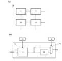
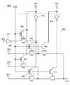
도 1의 (a)는 본 발명의 일 실시 형태에 따른 PLD(프로그래머블 로직 디바이스)의 구성을 도시하는 블록도이다.1A is a block diagram showing the configuration of a PLD (Programmable Logic Device) according to an embodiment of the present invention.
도 1의 (a)에 도시한 바와 같이, PLD(10)는 복수의 PLE(프로그래머블 로직 엘리먼트)(11)를 포함한다. PLE(11) 간의 전기적 접속은, PLE(11) 사이의 접속을 정의하기 위한 정보를 포함하는 컨피규레이션 데이터에 따라 제어된다.As shown in Fig. 1A, the
구체적으로, PLE(11)는 복수의 배선을 포함하는 배선군과, 배선군에 포함되는 배선 사이의 접속을 컨피규레이션 데이터에 따라서 제어하는 스위치를 포함하는 배선 엘리먼트에 의해 서로 접속될 수 있다.Specifically, the
도 1의 (b)는 PLE(11)의 구성예를 도시하는 블록도이다. PLE(11)는 LUT(룩업 테이블)(12)과, FF(플립플롭)(13)과, MUX(멀티플렉서)(14)를 적어도 포함한다.1B is a block diagram showing an example of the configuration of the
LUT(12)에는, LUT(12)의 논리 게이트로서의 기능을 정의하기 위한 데이터를 포함하는 컨피규레이션 데이터(18)가 입력된다. 즉, 단자(16)로부터 LUT(12)에 입력되는 신호의 논리 레벨과, LUT(12)로부터 출력되는 출력 신호의 논리 레벨의 관계는 컨피규레이션 데이터(18)에 따라서 정해진다.The
FF(13)에는, LUT(12)로부터의 출력 신호가 입력된다. 하나의 PLE(11)에 포함되는 FF(13)로부터의 출력 신호가, 다른 PLE(11)에 포함되는 FF(13)에 입력될 수도 있다. FF(13)는 입력된 이 신호를 유지하는 기능을 갖는다.The output signal from the
MUX(14)에는, MUX(14)의 동작을 제어하기 위한 데이터를 포함하는 컨피규레이션 데이터(19)가 입력된다. MUX(14)는, LUT(12)로부터의 출력 신호와, FF(13)로부터의 출력 신호의 어느 하나를, 컨피규레이션 데이터(19)에 따라서 선택하는 기능을 갖는다. MUX(14)에 의해 선택된 신호는, PLE(11)의 단자(17)로부터 출력된다.The
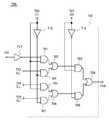
<멀티플렉서의 구성예><Configuration example of multiplexer>
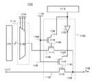
도 2에, MUX(14)의 구체적인 구성예를 나타낸다. 도 2에 도시하는 MUX(14)는, 스위치(20a) 및 스위치(20b)를 적어도 포함한다. MUX(14)는, CM(컨피규레이션 메모리)(15)로부터 입력되는 컨피규레이션 데이터를 포함하는 신호에 따라, 스위치(20a) 및 스위치(20b)의 동작을 제어함으로써, 복수의 배선(25)에 입력된 신호 중 어느 하나를 선택하는 기능과, 선택된 신호를 배선(26)에 공급하는 기능을 갖는다. 컨피규레이션 메모리는 컨피규레이션 데이터를 기억하는 레지스터에 상당한다.2 shows a specific configuration example of the
배선(25a)을 복수의 배선(25) 중 하나로 가정하면, 구체적으로, 스위치(20a)는 CM(15)로부터 입력되는 컨피규레이션 데이터를 포함하는 신호에 따라, 배선(25a)에 입력된 신호를 배선(26a)에 공급할지의 여부를 제어하는 기능을 갖는다. 또한, 배선(25b)을 복수의 배선(25) 중 다른 하나라고 가정하면, 구체적으로, 스위치(20b)는 CM(15)로부터 입력되는 컨피규레이션 데이터를 포함하는 신호에 따라, 배선(25b)에 입력된 신호를 배선(26b)에 공급할지의 여부를 제어하는 기능을 갖는다.Assuming that the
스위치(20a) 및 스위치(20b)는, 각각 트랜지스터(21) 및 트랜지스터(22)를 포함한다. 트랜지스터(21)는 컨피규레이션 데이터를 포함하는 신호의, 트랜지스터(22)의 게이트에의 입력을 제어하는 기능을 갖는다. 트랜지스터(22)는, 트랜지스터(22)의 게이트에 입력된 컨피규레이션 데이터를 포함하는 신호에 따라, 도통 상태 또는 비도통 상태가 정해진다. 트랜지스터(22)가 도통 상태일 때, 배선(25a) 또는 배선(25b)에 입력된 신호가 트랜지스터(22)를 개재해서 배선(26a)에 공급된다. 반대로, 트랜지스터(22)가 비도통 상태일 때, 배선(25a) 또는 배선(25b)에 입력된 신호는 배선(26a)에 공급되지 않는다.The
구체적으로, 트랜지스터(21)의 소스 및 드레인의 한쪽에, 컨피규레이션 데이터를 포함하는 신호가 입력되고, 트랜지스터(21)의 소스 및 드레인의 다른 쪽이 트랜지스터(22)의 게이트에 접속되고 있다. 트랜지스터(22)의 소스 및 드레인의 한쪽이 배선(25a) 또는 배선(25b)에 접속되어 있고, 트랜지스터(22)의 소스 및 드레인의 다른 쪽이 배선(26a)에 접속되고 있다.Specifically, a signal including a configuration data is input to one of the source and drain of the
스위치(20a)와 스위치(20b)에 입력되는 컨피규레이션 데이터를 포함하는 신호의 논리 레벨은 서로 상이하다. 구체적으로, 도 2에서는, 스위치(20a)에 입력되는 신호의 논리 레벨을 인버터(27)에 의해 반전시킨 신호가, 스위치(20b)에 입력되는 경우를 예시하고 있다. 단, 인버터(27)를 사용하지 않고, 스위치(20a)와 스위치(20b)에 논리 레벨이 서로 다른 상기 신호가 입력되도록 해도 된다.Logic levels of signals including configuration data input to the
도 2에서는, 인버터(27)가 MUX(14)에 포함되지 않는 경우를 예시하고 있지만, MUX(14)는 인버터(27)를 포함하고 있어도 된다.In FIG. 2, the case where the
상기 구성에 의해, 스위치(20a) 및 스위치(20b)의 어느 한쪽이 트랜지스터(22)에 의해 도통 상태로 되고, 스위치(20a) 및 스위치(20b)의 다른 쪽이 트랜지스터(22)에 의해 비도통 상태로 된다. 즉, 배선(25a) 및 배선(25b)에 입력된 신호 중 어느 한쪽만이 스위치(20a) 및 스위치(20b)에 의해 선택되어서, 배선(26a)에 공급된다.With the above configuration, either one of the
복수의 배선(25)의 수에 따라서는, MUX(14)에 복수의 스위치(20a) 및 복수의 스위치(20b)를 제공하는 경우도 있을 수 있다. 그 경우, MUX(14)에는, 복수의 스위치(20a) 및 스위치(20b)에 의해 선택된 신호가 입력되는 배선(26a)이 복수 존재 하게 된다. 상기 경우의 MUX(14)는, 복수의 배선(26a)에 입력되는 신호를 선택하기 위한 단수 또는 복수의 스위치(20a) 및 단수 또는 복수의 스위치(20b)를 더 포함한다. 복수의 스위치(20a) 및 복수의 스위치(20b)에 의해 반복적으로 신호를 선택함으로써, 최종적으로 1개의 신호가 배선(26)에 공급된다.Depending on the number of the plurality of wirings 25, the
그리고, 본 발명의 일 실시 형태에서는, 트랜지스터(21)는 트랜지스터(22)에 비하여 오프 전류가 현저하게 작은 것으로 한다. 실리콘보다 밴드갭이 넓고, 진성 캐리어 밀도가 실리콘보다 낮은 반도체 막에 채널 형성 영역이 형성되는 트랜지스터는, 오프 전류를 현저하게 작게 할 수 있으므로, 트랜지스터(21)로서 사용하는 데에 적합하다. 이러한 반도체로서는, 예를 들어 실리콘보다 2배 이상 큰 밴드 갭을 갖는 산화물 반도체 및 질화갈륨 등을 들 수 있다. 상기 반도체를 포함하는 트랜지스터는, 통상의 실리콘이나 게르마늄 등의 반도체를 포함하는 트랜지스터에 비하여 오프 전류를 상당히 작게 할 수 있다.In addition, in one embodiment of the present invention, it is assumed that the off current of the
상기 구성을 갖는 트랜지스터(21)는, 트랜지스터(21)가 비도통 상태일 때에, 트랜지스터(22)의 게이트에 접속된 노드 SN에 유지되고 있는 전하가 누설되는 것을 방지할 수 있다. 노드 SN에 전하가 유지됨으로써, 트랜지스터(22)의 도통 상태 또는 비도통 상태가 유지되므로, 스위치(20a) 및 스위치(20b)에 의해 신호가 계속 선택된다.The
스위치(20a) 및 스위치(20b)에서는, 트랜지스터(21)가 비도통 상태에 있을 때 노드 SN이 부유 상태가 되기 때문에, 이하에 설명하는 부스팅 효과를 기대할 수 있다. 즉, 스위치(20a) 및 스위치(20b)에서는, 노드 SN이 부유 상태에 있으면, 배선(25a) 또는 배선(25b)의 전위가 로우 레벨로부터 하이 레벨로 변화함에 따라, 트랜지스터(22)의 소스와 게이트의 사이에 형성되는 용량 Cgs에 의해 노드 SN의 전위가 상승한다. 노드 SN의 전위의 상승 폭은, 트랜지스터(22)의 게이트에 입력된 컨피규레이션 데이터의 논리 레벨에 따라 상이하다. 구체적으로, 스위치(20a) 및 스위치(20b)에 기입된 컨피규레이션 데이터가 "0"인 경우, 트랜지스터(22)는 약반전 모드(weak inversion mode)에 있기 때문에, 노드 SN의 전위의 상승에 기여하는 용량 Cgs에는, 게이트 전극의 전위, 즉 노드 SN의 전위에 의존하지 않는 용량 Cos가 포함된다. 구체적으로, 용량 Cos에는, 예를 들어 게이트 전극과 소스 영역이 서로 중첩하는 영역에 형성되는 오버랩 용량과, 게이트 전극과 소스 전극의 사이에 형성되는 기생 용량이 포함된다. 한편, 스위치(20a) 및 스위치(20b)에 기입된 컨피규레이션 데이터가 "1"인 경우, 트랜지스터(22)는 강반전 모드(strong inversion mode)에 있기 때문에, 노드 SN의 전위의 상승에 기여하는 용량 Cgs에는, 상술한 용량 Cos 외에, 게이트 전극과 드레인 전극의 사이에 형성되는 용량 Cod와, 채널 형성 영역과 게이트 전극의 사이에 형성되는 용량 Cox의 일부가 포함된다. 따라서, 컨피규레이션 데이터가 "1"인 경우, 노드 SN의 전위의 상승에 기여하는 용량 Cgs가, 컨피규레이션 데이터가 "0"인 경우의 용량 Cgs보다 크다. 따라서, 스위치(20a) 및 스위치(20b)에서는, 배선(25a) 또는 배선(25b)의 전위의 변화에 수반하여 컨피규레이션 데이터가 "1"인 경우의 노드 SN의 전위가 컨피규레이션 데이터가 "0"인 경우의 노드 SN의 전위보다 높아지는 부스팅 효과를 얻을 수 있다. 따라서, 컨피규레이션 데이터가 "1"인 경우에, 트랜지스터(21)의 역치 전압만큼 노드 SN의 전위가 강하하는 경우에도, 부스팅 효과에 의해 노드 SN의 전위를 상승시킬 수 있으므로, 트랜지스터(22)의 도통 상태를 확보할 수 있고, 스위치(20a) 및 스위치(20b)의 스위치 속도를 향상시킬 수 있다. 컨피규레이션 데이터가 "0"인 경우에는, 트랜지스터(22)의 비도통 상태를 확보할 수 있다.In the
본 발명의 일 실시 형태에서는, PLD에 공급하는 전원 전압을 작게 함으로써, 트랜지스터(22)의 게이트에 입력되는 신호의 전압이 작아져도, 즉, 당해 게이트에 부여되는 전위가 낮아져도, 상기 부스팅 효과에 의해 스위치 MUX(14)를 정상적으로 동작시킬 수 있다. 따라서, PLD에 공급하는 전원 전압을 작게 해도, PLE로부터 출력되는 신호의 논리 레벨이 변화하는 것을 방지하고, PLD가 정상적으로 동작하지 않는 사태가 발생할 수 있는 것을 방지할 수 있다.In one embodiment of the present invention, by reducing the power supply voltage supplied to the PLD, even if the voltage of the signal input to the gate of the
<스위치의 동작예><Switch operation example>
계속해서, 도 2에 도시한 스위치(20a) 및 스위치(20b)의 동작예에 대해서 설명한다. 도 3의 (a)에, 도 2에 도시한 스위치(20a) 및 스위치(20b)와 배선의 접속예를 나타낸다. 도 3의 (b)에, 배선에 입력되는 신호와, 트랜지스터(22)의 게이트에 접속된 노드 SN의 전위의 타이밍 차트의 일례를 나타낸다.Subsequently, an operation example of the
도 3의 (a)에 나타내는 스위치(20a) 및 스위치(20b) 각각에서는, 트랜지스터(21)의 게이트가 배선(23)에 접속되고 있다. 스위치(20a)의 트랜지스터(21)의 그 소스 및 드레인 중 한쪽은 배선(24)에 접속되어 있다. 스위치(20b)의 트랜지스터(21)의 그 소스 및 드레인 중 한쪽은 인버터(27)의 출력 단자에 접속되고 있다. 인버터(27a)의 입력 단자는 배선(24)에 접속되고 있다.In each of the
도 3의 (b)에 도시한 바와 같이, 기간 T1에서 배선(23)에 하이 레벨인 전위가 부여되면, 스위치(20a) 및 스위치(20b) 각각에서 트랜지스터(21)가 도통 상태가 된다. "1"의 논리 레벨에 대응하는 하이 레벨인 전위가 배선(24)에 부여되면, 스위치(20a)에서는 노드 SN에 "1"의 논리 레벨에 대응하는 하이 레벨인 전위가 트랜지스터(21)를 개재해서 부여된다. 스위치(20b)에서는 노드 SN에 "0"의 논리 레벨에 대응하는 로우 레벨의 전위가 트랜지스터(21)를 개재해서 부여된다. 스위치(20a)에서 노드 SN에 부여되는 전위는 배선(24)의 전위보다 트랜지스터(21)의 역치 전압만큼 강하하고 있다.As shown in Fig. 3(b), when a high level potential is applied to the
기간 T1 후에, 배선(23)에 로우 레벨의 전위가 부여된다. 그 후에, 스위치(20a) 및 스위치(20b) 각각에서 트랜지스터(21)는 비도통 상태로 된다. 따라서, 스위치(20a) 및 스위치(20b) 각각에서 노드 SN의 전위가 유지된다.After the period T1, the low level potential is applied to the
계속해서, 기간 T2에서, 배선(25a)의 전위가 로우 레벨로부터 하이 레벨로 변화하고, 배선(25b)에 로우 레벨의 전위가 부여된다. 스위치(20a)에서는, 노드 SN이 부유 상태에 있고, 트랜지스터(22)가 강반전 모드에 있어, 부스팅 효과에 의해, 배선(25a)의 전위가 로우 레벨로부터 하이 레벨로 변화함에 따라, 노드 SN의 전위가 더 상승한다. 한편, 스위치(20b)에서는, 배선(25b)에는 로우 레벨의 전위가 부여되고, 트랜지스터(22)는 약반전 모드에 있어서, 노드 SN의 전위는 로우 레벨로 유지된다. 따라서, 스위치(20a)의 트랜지스터(22)가 도통 상태이고, 스위치(20b)의 트랜지스터(22)는 비도통 상태가 되어, 스위치(20a)를 개재해서 배선(25a)의 전위가 배선(26a)에 부여되고, 배선(26a)의 전위는 하이 레벨로 설정된다.Subsequently, in the period T2, the potential of the
계속해서, 기간 T3에서, 배선(25a)에 로우 레벨의 전위가 부여되고, 배선(25b)의 전위가 로우 레벨로부터 하이 레벨로 변화한다. 스위치(20a)에서는, 노드 SN이 부유 상태에 있고, 트랜지스터(22)가 강반전 모드에 있다. 그러나, 배선(25a)의 전위가 로우 레벨이므로, 노드 SN은 기간 T1에서 주어진 전위, 즉, 배선(24)의 전위보다 트랜지스터(21)의 역치 전압만큼 강하한 전위가 유지된다. 한편, 스위치(20b)에서는 노드 SN이 부유 상태에 있기 때문에, 부스팅 효과에 의해, 배선(25b)의 전위가 로우 레벨로부터 하이 레벨로 변화함에 따라 노드 SN의 전위가 상승한다. 스위치(20b)에서는 트랜지스터(22)가 약반전 모드에 있기 때문에, 노드 SN의 전위의 상승 폭은, 기간 T2의 스위치(20a)에서의 노드 SN의 전위의 상승 폭보다 작다. 그로 인해, 스위치(20b)에서는 트랜지스터(22)가 비도통 상태를 유지한다. 따라서, 배선(25a)의 전위가 로우 레벨이고, 스위치(20b)의 트랜지스터(22)가 비도통 상태가 되어, 배선(26a)의 전위는 로우 레벨이 된다.Subsequently, in the period T3, a low level potential is applied to the
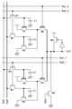
계속해서, 2비트의 신호가 입력되는 MUX(14)의 구성을 도 4에 일례로서 나타낸다. 도 4에 도시하는 MUX(14)는 6개의 스위치(20a 내지 20f)를 포함한다. 스위치(20a 내지 20f)는 각각 트랜지스터(21) 및 트랜지스터(22)를 포함한다. 트랜지스터(21)와 트랜지스터(22)의 접속 구조는 도 2에 도시하는 MUX(14)와 같다.Subsequently, the configuration of the
단, 도 4에 도시하는 MUX(14)에서는, 스위치(20a) 및 스위치(20c) 각각에 포함되는 트랜지스터(21)는 소스 및 드레인 중 한쪽이 컨피규레이션 데이터를 포함하는 신호가 입력되는 배선(24a)에 접속되고 있다. 스위치(20b) 및 스위치(20d) 각각의 트랜지스터(21)는 소스 및 드레인 중 한쪽이 인버터(27a)의 출력 단자에 접속되고 있다. 인버터(27)의 입력 단자는 배선(24a)에 접속되고 있다. 또한, 스위치(20e)에 포함되는 트랜지스터(21)는 소스 및 드레인 중 한쪽이 컨피규레이션 데이터를 포함하는 신호가 입력되는 배선(24b)에 접속되고 있다. 스위치(20f)의 트랜지스터(21)는 소스 및 드레인 중 한쪽이 인버터(27b)의 출력 단자에 접속되고 있다. 인버터(27b)의 입력 단자는 배선(24b)에 접속되고 있다.However, in the
또한, 도 4에 도시하는 MUX(14)에서는, 스위치(20a 내지 20d)가 각각 갖는 트랜지스터(22)는 소스 및 드레인 중 한쪽이 배선(25a, 25b, 25c, 25d)에 각각 접속되고 있다. 스위치(20a) 및 스위치(20b)가 각각 갖는 트랜지스터(22)는 소스 및 드레인 중 다른 쪽이, 스위치(20e)가 갖는 트랜지스터(22)의 소스 및 드레인 중 한쪽에 접속되고 있다. 스위치(20c) 및 스위치(20d)가 각각 갖는 트랜지스터(22)는 소스 및 드레인 중 다른 쪽이, 스위치(20f)가 갖는 트랜지스터(22)의 소스 및 드레인 중 한쪽에 접속되고 있다. 스위치(20e) 및 스위치(20f)가 각각 갖는 트랜지스터(22)의 소스 및 드레인 중 다른 쪽은, 배선(26)에 접속되고 있다.In the
도 4에 도시하는 MUX(14)에서는, 배선(24a) 및 배선(24b)으로부터 입력되는 컨피규레이션 데이터를 포함하는 신호에 따라 트랜지스터(22)의 도통 상태와 비도통 상태가 정해진다. 배선(25a 내지 25d)에 입력된 신호 중 어느 하나가, 컨피규레이션 데이터에 따라 스위치(20a 내지 20f)에 의해 선택되어, 배선(26)에 입력된다.In the
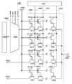
도 5에, 도 4에 도시한 MUX(14)와 마찬가지로 2비트의 신호가 공급되는, AO 게이트를 포함하는 MUX(40)의 구성을 나타낸다.5 shows a configuration of the
도 5에 도시하는 MUX(40)는, 3개의 AO 게이트(30)(AO 게이트(30a 내지 30c))를 포함한다. AO 게이트(30a 내지 30c)는 각각 AND 회로(31), AND 회로(32) 및 OR 회로(33)를 포함한다. AND 회로(31)의 출력 단자는 OR 회로(33)의 제1 입력 단자에 접속된다. AND 회로(32)의 출력 단자는 OR 회로(33)의 제2 입력 단자에 접속되고 있다.The
AO 게이트(30a)에서는, AND 회로(31)의 제1 입력 단자가 배선(25a)에 접속되어 있고, AND 회로(31)의 제2 입력 단자가 배선(24a)에 접속되고 있다. AO 게이트(30a)에서는, AND 회로(32)의 제1 입력 단자가 배선(25b)에 접속되어 있고, AND 회로(32)의 제2 입력 단자가 인버터(27a)의 출력 단자에 접속되고 있다. 인버터(27)의 입력 단자는 배선(24a)에 접속되고 있다.In the
AO 게이트(30b)에서는, AND 회로(31)의 제1 입력 단자가 배선(25c)에 접속되어 있고, AND 회로(31)의 제2 입력 단자가 배선(24a)에 접속되고 있다. AO 게이트(30b)에서는, AND 회로(32)의 제1 입력 단자가 배선(25d)에 접속되어 있고, AND 회로(32)의 제2 입력 단자가 인버터(27a)의 출력 단자에 접속되고 있다.In the
AO 게이트(30c)에서는, AND 회로(31)의 제1 입력 단자가, AO 게이트(30a)가 갖는 OR 회로(33)의 출력 단자에 접속되어 있고, AND 회로(31)의 제2 입력 단자가 배선(24b)에 접속되고 있다. AO 게이트(30c)에서는, AND 회로(32)의 제1 입력 단자가, AO 게이트(30b)가 갖는 OR 회로(33)의 출력 단자에 접속되어 있고, AND 회로(32)의 제2 입력 단자가 인버터(27b)의 출력 단자에 접속되고 있다. 인버터(27b)의 입력 단자는 배선(24b)에 접속되고 있다. AO 게이트(30c)가 갖는 OR 회로(33)의 출력 단자는 배선(26)에 접속되고 있다.In the
도 5에 도시하는 MUX(40)에서는, 각 배선(25a 내지 25d)과 배선(26)의 사이에, 복수의 논리 게이트(예를 들면, AND 회로(31), AND 회로(32) 및 OR 회로(33))가 접속되고 있다. 한편, 도 4에 도시하는 MUX(14)에서는, 각 배선(25a 내지 25d)과 배선(26)의 사이에는, 2개의 트랜지스터(22)가 서로 직렬로 접속되고 있다. AND 회로는 NAND 회로와 인버터의 조합이고, OR 회로는 NOR 회로와 인버터의 조합이다. 따라서, 게이트 단수, 바꾸어 말하면, 트랜지스터의 게이트와 소스 또는 드레인 사이에서 행하여지는 신호의 전달 횟수는, MUX(14)의 스위치(20)에서는 0인 것에 반해, MUX(40)의 AO 게이트(30)에서의 게이트 단수, 즉 신호의 전달 횟수는 4이다. MUX(14)에서는, 상술한 부스팅 효과에 의해, 트랜지스터(22)의 역치 전압에 의한 2개의 트랜지스터(22)를 통한 배선(26)에 입력되는 신호의 전압의 강하가 거의 발생하지 않는다. 그로 인해, 본 발명의 일 실시 형태에 따른 MUX(14)의 신호 지연 시간이 복수의 논리 게이트를 포함하는 MUX(40)보다 짧다.In the
본 명세서에서, 트랜지스터가 서로 직렬로 접속되고 있는 상태는, 예를 들어 제1 트랜지스터의 소스 및 드레인의 한쪽만이, 제2 트랜지스터의 소스 및 드레인의 한쪽에만 접속되고 있는 상태를 의미한다. 또한, 트랜지스터가 서로 병렬로 접속되고 있는 상태는, 제1 트랜지스터의 소스 및 드레인의 한쪽이 제2 트랜지스터의 소스 및 드레인의 한쪽에 접속되고, 제1 트랜지스터의 소스 및 드레인의 다른 쪽이 제2 트랜지스터의 소스 및 드레인의 다른 쪽에 접속되고 있는 상태를 의미한다.In this specification, the states in which the transistors are connected in series with each other means, for example, a state in which only one of the source and the drain of the first transistor is connected to only one of the source and the drain of the second transistor. In the state in which the transistors are connected in parallel to each other, one of the source and drain of the first transistor is connected to one of the source and the drain of the second transistor, and the other of the source and drain of the first transistor is the second transistor. It means that the source and drain are connected to the other side.
회로의 동적 소비 전력 P는 수학식 1로 표현된다. 단, α, f, n, Cload 및 Vd는 활성화율, 동작 주파수, 소자수, 소자의 부하 용량 및 전원 전압을 각각 의미한다.The dynamic power consumption P of the circuit is expressed by equation (1). However, α, f, n, Cload and Vd refer to activation rate, operating frequency, number of devices, load capacity of devices, and power supply voltage, respectively.
[수학식 1][Equation 1]
P=α×f×Cload×Vd2×nP=α×f×Cload ×Vd2 ×n
MUX(40)에서는, AO 게이트(30a 내지 30c)는 각각 AND 회로(31), AND 회로(32) 및 OR 회로(33)를 포함한다. 배선(25a 및 25b)의 하나에 입력되는 신호는 AND 회로(31 및 32)의 어느 하나와, OR 회로(33)를 경유하여, 배선(26)에 입력된다. 따라서, 배선(24a 및 24b)으로부터 입력되는 신호의 논리 레벨이 일정한 경우, AO 게이트(30a 내지 30c) 각각의 게이트의 단수가 4이며, 각 단의 활성화율이 1/2이므로, 활성화율 α는 2가 된다.In
도 5에 도시하는 AND 회로(31) 및 AND 회로(32)를 NAND 회로로 변경하고, OR 회로(33)를 NAND 회로로 변경해도, 논리 게이트로서의 기능은 AO 게이트(30)와 같다. 3개의 NAND 회로로 구성되는 논리 게이트를 MUX(40)가 포함하는 경우, 각 논리 게이트의 게이트 단수는 2이며, 각 단의 활성화율이 1/2이므로, 활성화율 α는 1이 된다.Even if the AND
한편, MUX(14)에서는, 소자수 n은 각 논리 게이트의 게이트 단수가 2인 MUX(40)보다 적다. 따라서, 수학식 1은, MUX(14)의 소비 전력 P가, 각 논리 게이트의 게이트 단수가 2인 MUX(40)의 소비 전력보다 상당히 작게 억제되는 것을 나타낸다.On the other hand, in the
각 논리 게이트의 게이트 단수가 2인 MUX(40)는 누설 전류 또는 관통 전류의 경로를 다수 갖고, MUX(14)의 누설 전류 또는 관통 전류의 경로의 수는 각 논리 게?堧? 게이트 단수가 2인 MUX(40)에 비해서 적다. 따라서, 누설 전류 또는 관통 전류에 기인하는 소비 전력은, MUX(40)보다 MUX(14) 쪽이 더 낮다.The number of gates of each
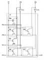
<LUT의 구성예><LUT configuration example>
계속해서, 도 6에 LUT(12)의 구성을 일례로서 나타낸다. 도 6에 나타내는 LUT(12)는, 2개의 AND 회로의 출력 단자가 OR 회로의 2개의 입력 단자에 접속된 AO 게이트(50)를 복수 포함한다.Subsequently, the configuration of the
구체적으로, 도 6에 나타내는 LUT(12)는 복수의 AO 게이트(50)(AO 게이트(50a 내지 50o))를 포함한다. 구체적으로, LUT(12)에서는, AO 게이트(50a 및 50b)의 후단에 AO 게이트(50i)가 접속되고 있다. AO 게이트(50c 및 50d)의 후단에 AO 게이트(50j)가 접속되고 있다. AO 게이트(50e 및 50f)의 후단에 AO 게이트(50k)가 접속되고 있다. AO 게이트(50g 및 50h)의 후단에 AO 게이트(50l)가 접속되고 있다. AO 게이트(50i 및 50j)의 후단에 AO 게이트(50m)가 접속되고 있다. AO 게이트(50k 및 50l)의 후단에 AO 게이트(50n)가 접속되고 있다. AO 게이트(50m 및 50n)의 후단에 AO 게이트(50o)가 접속되고 있다.Specifically, the
각 AO 게이트(50)는, AND 회로(51)와, AND 회로(52)와, OR 회로(53)를 포함한다. AND 회로(51)의 출력 단자와 AND 회로(52)의 출력 단자가, OR 회로(53)의 2개의 입력 단자에 접속되고 있다. 각 AO 게이트(50)에서는, AND 회로(51)의 제1 입력 단자와, AND 회로(52)의 제1 입력 단자가, 복수의 배선(54)의 하나, 또는 전단의 AO 게이트(50)에 포함되는 OR 회로(53)의 출력 단자에 접속되고 있다. AND 회로(51)의 제2 입력 단자가, 컨피규레이션 데이터를 포함하는 신호가 입력되는 복수의 배선(56)의 하나에 접속되고 있다. AND 회로(52)의 제2 입력 단자가 복수의 인버터(57)(인버터(57a 내지 57d)) 중 어느 하나의 출력 단자에 접속되고 있다. 인버터(57a 내지 57d)의 입력 단자는 복수의 배선(56)에 접속되고 있다. 최종단의 AO 게이트(50o)에 포함되는 OR 회로(53)의 출력 단자는 배선(55)에 접속되고 있다.Each AO gate 50 includes an AND
본 발명의 일 실시 형태에서는, AND 회로(51), AND 회로(52), OR 회로(53) 및 인버터(57a 내지 57d)는 슈미트 트리거 논리 게이트이다. 슈미트 트리거 논리 게이트를 LUT(12)에 사용함으로써, PLD에 공급하는 전원 전압이 작아지더라도, 멀티플렉서와 LUT(12)가 정상적인 동작을 할 수 있어, LUT(12)의 동작 속도의 저하를 방지할 수 있다.In one embodiment of the present invention, the AND
<슈미트 트리거 논리 게이트의 구성예><Configuration example of Schmitt trigger logic gate>
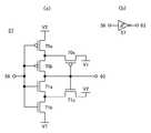
도 7의 (a)에, 인버터(57)의 구성을 일례로서 나타낸다. 단, 도 7의 (a)에 나타내는 인버터(57)는, 도 7의 (b)에 도시한 바와 같이, 입력 단자 및 출력 단자가 배선(56) 및 배선(63)에 각각 접속되고 있는 것으로 한다.7A shows the configuration of the
도 7의 (a)에 나타내는 인버터(57)는 p채널형의 트랜지스터(70a 내지 70c)와, n채널형의 트랜지스터(71a 내지 71c)를 포함한다. 트랜지스터(71a 및 71b)는 배선(63)과, 전위 V1이 부여되는 배선과의 사이에서 서로 직렬로 접속되고 있다. 트랜지스터(71c)는, 트랜지스터(71a)의 소스 및 드레인의 한쪽과, 트랜지스터(71b)의 소스 및 드레인의 한쪽이 접속된 노드와, 전위 V1보다 높은 전위 V2가 부여되는 배선 간의 전기적인 접속을, 배선(63)의 전위에 따라서 제어하는 기능을 갖는다. 트랜지스터(70a 및 70b)는 배선(63)과, 전위 V2가 부여되는 배선의 사이에서 서로 직렬로 접속되고 있다. 트랜지스터(70c)는 트랜지스터(70a)의 소스 및 드레인의 한쪽과, 트랜지스터(70b)의 소스 및 드레인의 한쪽이 접속된 노드와, 전위 V1이 부여되는 배선 간의 전기적인 접속을, 배선(63)의 전위에 따라서 제어하는 기능을 갖는다. 트랜지스터(70a 및 70b)와, 트랜지스터(71a 및 71b)는 게이트가 배선(56)에 접속되고 있다.The
PLD에 부여되는 전원 전압이 낮아지면, 배선(56)에 부여되는 로우 레벨의 전위와 하이 레벨의 전위의 차가 작아진다. 이 경우, 인버터(57)에 포함되는 트랜지스터의 역치 전압에 따라서는, 배선(56)의 전위가 로우 레벨일 때에도, 트랜지스터(71a)와 트랜지스터(71b)를 완전히 비도통 상태로 할 수 없고, 혹은, 배선(56)의 전위가 하이 레벨일 때에도, 트랜지스터(70a)와 트랜지스터(70b)를 완전히 비도통 상태로 할 수 없다. 그로 인해, 배선(63)의 전위가 하이 레벨이 되어야 할 때에 당해 전위가 저하되거나, 배선(63)의 전위가 로우 레벨이 되어야 할 때에 당해 전위가 상승하는 경우가 있을 수 있다.When the power supply voltage applied to the PLD decreases, the difference between the low level potential and the high level potential applied to the
그러나, 도 7의 (a)에 도시된 바와 같은 슈미트 트리거 인버터(57)에서는, 예를 들어 배선(56)에 로우 레벨의 전위가 부여되고 있을 때에, 트랜지스터(70a) 및 트랜지스터(70b)뿐만 아니라, 트랜지스터(71c)도 도통 상태로 된다. 따라서, 트랜지스터(71a)의 소스와 드레인에 전위 V2를 부여할 수 있다. 따라서, 트랜지스터(71a)의 드레인 전류를 거의 0으로 하여, 배선(63)의 전위가 저하되는 것을 방지할 수 있다. 반대로, 예를 들어 배선(56)에 하이 레벨의 전위가 부여되고 있을 때에, 트랜지스터(71a) 및 트랜지스터(71b) 뿐만 아니라, 트랜지스터(70c)도 도통 상태로 된다. 따라서, 트랜지스터(70b)의 소스와 드레인에 전위 V1을 부여할 수 있다. 따라서, 트랜지스터(70b)의 드레인 전류를 0에 접근시켜서, 배선(63)의 전위가 상승하는 것을 방지할 수 있다.However, in the
계속해서, 도 8의 (a)에, AND 회로(51)의 구성을 일례로서 나타낸다. 단, 도 8의 (a)에 나타내는 AND 회로(51)는, 도 8의 (b)에 도시한 바와 같이, 제1 입력 단자, 제2 입력 단자 및 출력 단자가, 배선(60), 배선(61) 및 배선(62)에 각각 접속되고 있는 것으로 한다. AND 회로(52)는 도 8의 (a)에 나타내는 AND 회로(51)와 동일한 구성을 갖고 있어도 된다.Subsequently, the structure of the AND
도 8의 (a)에 나타내는 AND 회로(51)는 p채널형의 트랜지스터(72a 내지 72e)와, n채널형의 트랜지스터(73a 내지 73e)와, 슈미트 트리거 인버터(74)를 포함한다. 인버터(74)이 구체적인 구성에 대해서는 도 7의 (a)를 참조할 수 있다.The AND
트랜지스터(72a 및 72b)는, 전위 V2가 부여되는 배선과, 인버터(74)의 입력 단자의 사이에서 서로 직렬로 접속되고 있다. 트랜지스터(72c 및 72d)는, 전위 V2가 부여되는 배선과, 인버터(74)의 입력 단자의 사이에서 서로 직렬로 접속되고 있다. 트랜지스터(72e)는, 트랜지스터(72a)의 소스 및 드레인의 한쪽과, 트랜지스터(72b)의 소스 및 드레인의 한쪽과, 트랜지스터(72c)의 소스 및 드레인의 한쪽과, 트랜지스터(72d)의 소스 및 드레인의 한쪽이 접속된 노드와, 전위 V1이 부여되는 배선 사이의 전기적인 접속을, 인버터(74)의 입력 단자의 전위에 따라서 제어하는 기능을 갖는다. 트랜지스터(73a 내지 73d)는, 인버터(74)의 입력 단자와, 전위 V1이 부여되는 배선의 사이에서 서로 직렬로 접속되고 있다. 트랜지스터(73e)는, 트랜지스터(73b)의 소스 및 드레인의 한쪽과, 트랜지스터(73c)의 소스 및 드레인의 한쪽이 접속된 노드와, 전위 V2가 부여되는 배선의 사이의 전기적인 접속을, 인버터(74)의 입력 단자의 전위에 따라서 제어하는 기능을 갖는다. 인버터(74)의 출력 단자는 배선(62)에 접속되고 있다. 트랜지스터(72a 및 72b)와 트랜지스터(73a 및 73c)는 게이트가 배선(60)에 접속되고 있다. 트랜지스터(72c 및 72d)와 트랜지스터(73b 및 73d)는 게이트가 배선(61)에 접속되고 있다.The
도 8의 (a)에 나타내는 AND 회로(51)는, 도 7의 (a)에 나타낸 인버터(57)와 마찬가지로, PLD에 부여되는 전원 전압이 낮아져도, 배선(62)의 전위가 하이 레벨이 되어야 할 때에 당해 전위가 저하되거나, 배선(62)의 전위가 로우 레벨이 되어야 할 때에 당해 전위가 상승하는 것을 방지할 수 있다.In the AND
계속해서, 도 9의 (a)에, OR 회로(53)의 구성을 일례로서 나타낸다. 단, 도 9의 (a)에 나타내는 OR 회로(53)는, 도 9의 (b)에 도시한 바와 같이, 제1 입력 단자, 제2 입력 단자 및 출력 단자가 배선(64), 배선(65) 및 배선(67)에 각각 접속되고 있는 것으로 한다.Subsequently, the structure of the
도 9의 (a)에 나타내는 OR 회로(53)는, p채널형의 트랜지스터(75a 내지 75e)와, n채널형의 트랜지스터(76a 내지 76e)와, 슈미트 트리거 인버터(77)를 포함한다. 인버터(77)의 구체적인 구성에 대해서는 도 7의 (a)를 참조할 수 있다.The OR
트랜지스터(75a 내지 75d)는, 전위 V2가 부여되는 배선과, 인버터(77)의 입력 단자의 사이에서 서로 직렬로 접속되고 있다. 트랜지스터(75e)는, 트랜지스터(75b)의 소스 및 드레인의 한쪽과, 트랜지스터(75c)의 소스 및 드레인의 한쪽이 접속된 노드와, 전위 V1이 부여되는 배선의 사이의 전기적인 접속을, 인버터(77)의 입력 단자의 전위에 따라서 제어하는 기능을 갖는다. 트랜지스터(76a 및 76b)는, 인버터(77)의 입력 단자와, 전위 V1이 부여되는 배선의 사이에서 서로 직렬로 접속되고 있다. 트랜지스터(76c 및 76d)는, 인버터(77)의 입력 단자와, 전위 V1이 부여되는 배선의 사이에서 서로 직렬로 접속되고 있다. 트랜지스터(76e)는, 트랜지스터(76a)의 소스 및 드레인의 한쪽과, 트랜지스터(76b)의 소스 및 드레인의 한쪽과, 트랜지스터(76c)의 소스 및 드레인의 한쪽과, 트랜지스터(76d)의 소스 및 드레인의 한쪽이 접속된 노드와, 전위 V2가 부여되는 배선의 사이의 전기적인 접속을, 인버터(77)의 입력 단자의 전위에 따라서 제어하는 기능을 갖는다. 인버터(77)의 출력 단자는 배선(67)에 접속되고 있다. 트랜지스터(75a 및 75c)와, 트랜지스터(76c 및 76d)는 게이트가 배선(64)에 접속되고 있다. 트랜지스터(75b 및 75d)와, 트랜지스터(76a 및 76b)는 게이트가 배선(65)에 접속되고 있다.The
도 9의 (a)에 나타내는 OR 회로(53)는, 도 7의 (a)에 나타낸 인버터(57)와 마찬가지로, PLD에 부여되는 전원 전압이 낮아져도, 배선(67)의 전위가 하이 레벨이 되어야 할 때에 당해 전위가 저하되거나, 배선(67)의 전위가 로우 레벨이 되어야 할 때에 당해 전위가 상승하는 것을 방지할 수 있다.In the
상술한 바와 같이, 슈미트 트리거 논리 게이트는, PLD의 전원 전압이 낮을 경우에도 논리 게이트로부터 출력되는 신호의 논리 레벨이 변화하는 것을 방지하는 장점을 갖는다. 그러나, 슈미트 트리거 논리 게이트는, CMOS를 사용한 통상의 논리 게이트에 비하여 소비 전력이 커진다는 단점을 가진다. 예를 들어, 도 7의 (a)에 나타낸 인버터(57)의 경우, 트랜지스터(71c)가 도통 상태인 동안에, 트랜지스터(71b)를 개재하여 전위 V1이 부여되는 배선과, 전위 V2가 부여되는 배선의 사이에 항상 흐르는 누설 전류에 의해, 소비 전력이 커진다. 한편, 스위치(20)(예를 들어, 도 3의 (a)의 스위치(20a) 또는 스위치(20b))를 포함하는 논리 게이트의 경우, PLD의 전원 전압이 낮을 때에도 논리 게이트로부터 출력되는 신호의 논리 레벨이 변화하는 것을 방지하는, 슈미트 트리거 논리 게이트와 같은 장점을 갖고, 슈미트 트리거 논리 게이트 또는 CMOS를 사용한 통상의 논리 게이트에 비하여 소비 전력이 작다는 장점도 갖는다.As described above, the Schmitt trigger logic gate has an advantage of preventing the logic level of the signal output from the logic gate from changing even when the power voltage of the PLD is low. However, the Schmitt-triggered logic gate has a drawback that power consumption is greater than that of a conventional logic gate using CMOS. For example, in the case of the
단, 스위치(20)를 포함하는 논리 게이트의 경우, 노드 SN에서의 전위의 논리 레벨이 유지되고 있는 경우에만 상술한 부스팅 효과를 얻을 수 있다. 도 3의 (a)에 나타내는 스위치(20a)를 예로 들어 설명하면, 스위치(20a)의 노드 SN에서의 전위의 재기입 빈도가 배선(25a)에 입력되는 신호의 논리 레벨이 변화하는 빈도보다 높은 경우, 상술한 부스팅 효과를 얻기 어렵다. 본 발명의 일 실시 형태에서처럼, 스위치(20)를 포함하는 논리 게이트를 MUX(14)에 사용하는 경우, 스위치(20)의 노드 SN에서의 전위의 재기입 빈도는 스위치(20)에서의 컨피규레이션 데이터의 재기입 빈도에 의존한다. 따라서, 스위치(20)의 노드 SN에서의 전위의 재기입 빈도는 배선(25)에 입력되는 신호의 논리 레벨이 변화하는 빈도보다 충분히 낮아지기 때문에, 부스팅 효과를 얻을 수 있다.However, in the case of the logic gate including the
그러나, LUT(12)에 스위치(20)를 포함하는 논리 게이트를 사용하는 경우, 배선(25)에는 컨피규레이션 데이터를 포함하는 신호가 입력되고, 배선(24)로부터 PLE(11)의 입력 신호가 입력된다. 따라서, 스위치(20)의 노드 SN에서의 전위의 재기입 빈도는, 배선(25)에 입력되는 신호의 논리 레벨이 변화하는 빈도보다 높아지기 때문에, 부스팅 효과를 얻기 어렵다. 본 발명의 일 실시 형태에 따른 PLD에서는, LUT(12)와 같이, 스위치(20)를 포함하는 논리 게이트를 사용하더라도 부스팅 효과를 얻기 어려운 최소한의 회로에 슈미트 트리거 논리 게이트를 사용하고, MUX(14)와 같이 부스팅 효과를 얻을 수 있는 회로에 스위치(20)를 포함하는 논리 게이트를 사용한다. 상기 구성에 의해, PLD에 공급하는 전원 전압이 감소하더라도, PLE로부터 출력되는 신호의 논리 레벨이 변화하는 것을 방지하고, PLD가 오작동하는 것을 방지할 수 있다.However, when a logic gate including a
<LUT의 구성예 2><Configuration example 2 of LUT>
계속해서, 도 10에 LUT(12)의 구성에 대해서 다른 일례를 나타낸다. 도 10에 도시하는 LUT(12)는 각각 3개의 NAND 회로를 포함하는 복수의 게이트(90)를 포함한다. 구체예로서, 도 10에서는, 3개의 게이트(90)(게이트(90a 내지 90c))를 포함하는 LUT(12)의 구성을 예시하고 있다.Subsequently, another example of the configuration of the
각 게이트(90)는 NAND 회로(91)와, NAND 회로(92)와, NAND 회로(93)를 포함한다. NAND 회로(91)의 출력 단자와 NAND 회로(92)의 출력 단자가 NAND 회로(93)에 2개의 입력 단자에 접속되고 있다. 각 게이트(90)에서는, NAND 회로(91)의 제1 입력 단자와, NAND 회로(92)의 제1 입력 단자가 복수의 배선(54) 중 하나 또는 전단의 게이트(90)에 포함되는 NAND 회로(93)의 출력 단자에 접속되고 있다. NAND 회로(91)의 제2 입력 단자가, 컨피규레이션 데이터를 포함하는 신호가 입력되는 복수의 배선(56) 중 하나에 접속되고 있다. NAND 회로(92)의 제2 입력 단자가 복수의 인버터(57)(인버터(57a 및 57b)) 중 어느 하나의 출력 단자에 접속되고 있다. 인버터(57a 및 57b)의 입력 단자는 복수의 배선(56)에 접속되고 있다. 최종단의 게이트(90c)에 포함되는 NAND 회로(93)의 출력 단자는 배선(55)에 접속되고 있다.Each gate 90 includes a
본 발명의 일 실시 형태에서는, NAND 회로(91), NAND 회로(92), NAND 회로(93) 및 인버터(57a 및 57b)는 슈미트 트리거 논리 게이트인 것으로 한다. 슈미트 트리거 논리 게이트를 LUT(12)에 사용함으로써, PLD에 공급하는 전원 전압이 작아지더라도, LUT(12)가 정상적으로 동작할 수 있다.In one embodiment of the present invention, it is assumed that the
<PLE의 구성예><Configuration example of PLE>
계속해서, 도 1의 (b)에 나타낸 PLE(11)의 구체적인 구성을, 도 11의 (a)에 일례로서 나타낸다. 도 11의 (a)에 나타내는 PLE(11)는, LUT(12)와, FF(13)와, MUX(14)와, LUT(12)의 컨피규레이션 데이터(18)가 기억되는 CM(18a)과, MUX(14)의 컨피규레이션 데이터(19)가 기억되는 CM(15)을 포함한다.Subsequently, a specific configuration of the
CM(18a)에 기억되고 있는 컨피규레이션 데이터에 따라, LUT(12)에 의해 실행되는 논리 연산이 변한다. 컨피규레이션 데이터에 의해, LUT(12)에 의해 행하여지는 논리 연산이 확정되면, LUT(12)는 단자(16)에 부여된 복수의 입력 신호에 대응하는 출력 신호를 생성한다. FF(13)는 LUT(12)에서 생성되는 출력 신호를 유지하고, 신호 CK에 동기하여, LUT(12)의 출력 신호에 대응한 출력 신호를 출력한다.The logical operation executed by the
MUX(14)에는, LUT(12)로부터의 출력 신호 및 FF(13)로부터의 출력 신호가 입력되고 있다. MUX(14)는, CM(15)에 저장되어 있는 컨피규레이션 데이터에 따라, 상기 2개의 출력 신호 중 어느 한쪽을 선택하고, 출력하는 기능을 갖는다. MUX(14)로부터의 출력 신호는 단자(17)에 입력된다.The output signal from the
다음으로, 도 1의 (b)에 나타낸 PLE(11)의 구체적인 구성의 다른 일례를, 도 11의 (b)에 나타낸다. 도 11의 (b)에 나타내는 PLE(11)는, MUX(80)와, MUX(80)의 컨피규레이션 데이터가 기억되는 CM(81)이 제공되는 점에서, 도 11의 (a)에 나타내는 PLE(11)와 상이하다.Next, another example of the specific configuration of the
MUX(80)에는, LUT(12)로부터의 출력 신호와, 다른 PLE(11)에 포함되는 FF(13)로부터의 출력 신호가 입력되고 있다. FF(13)로부터의 출력 신호는 단자(82)로부터 입력된다. MUX(80)는, CM(81)에 저장되어 있는 컨피규레이션 데이터에 따라, 상기 2개의 출력 신호 중 어느 한쪽을 선택하고, 출력하는 기능을 갖는다.The output signal from the
도 11의 (b)에 나타낸 PLE(11)에서는, FF(13)는 MUX(80)로부터의 출력 신호를 유지하고, 신호 CK에 동기하여 LUT(12)로부터의 출력 신호에 대응하는 출력 신호를 출력한다.In the
또한, 도 11의 (a) 또는 도 11의 (b)에 나타내는 PLE(11)에서는, 컨피규레이션 데이터에 의해 FF(13)의 종류를 정의하여도 된다. 구체적으로는, 컨피규레이션 데이터에 의해, FF(13)가 D형 플립플롭, T형 플립플롭, JK형 플립플롭 및 RS형 플립플롭의 어느 하나의 기능을 갖도록 해도 된다.In addition, in the
<PLD의 구성예 2><Configuration example 2 of PLD>
도 12의 (a)에 PLD(10)의 구조 일부를, 일례로서 모식적으로 도시한다. 도 12의 (a)에 나타내는 PLD(10)는, 복수의 PLE(11)와, 복수의 PLE(11) 중 어느 하나에 접속된 배선군(121)과, 배선군(121)에 포함되는 배선 간의 접속을 제어하는 스위치(122)를 포함한다. 배선군(121) 및 스위치(122)는 배선 리소스(123)에 상당한다. 스위치(122)에 의해 제어되는 배선끼리의 접속 구조는 컨피규레이션 데이터에 의해 정해진다.A part of the structure of the
도 12의 (b)에 스위치(122)의 구성예를 나타낸다. 도 12의 (b)에 나타내는 스위치(122)는, 배선군(121)에 포함되는 배선(125)과 배선(126)의 접속 구조를 제어하는 기능을 갖는다. 구체적으로, 스위치(122)는 트랜지스터(127 내지 132)를 포함한다. 트랜지스터(127)는 배선(125)에서의 포인트 A와, 배선(126)에서의 포인트 C의 전기적인 접속을 제어하는 기능을 갖는다. 트랜지스터(128)는, 배선(125)에서의 포인트 B와, 배선(126)에서의 포인트 C의 전기적인 접속을 제어하는 기능을 갖는다. 트랜지스터(129)는, 배선(125)에서의 포인트 A와, 배선(126)에서의 포인트 D의 전기적인 접속을 제어하는 기능을 갖는다. 트랜지스터(130)는, 배선(125)에서의 포인트 B와, 배선(126)에서의 포인트 D의 전기적인 접속을 제어하는 기능을 갖는다. 트랜지스터(131)는, 배선(125)에서의 포인트 A와 포인트 B의 전기적인 접속을 제어하는 기능을 갖는다. 트랜지스터(132)는, 배선(126)에서의 포인트 C와 포인트 D의 전기적인 접속을 제어하는 기능을 갖는다.An example of the configuration of the
각각의 트랜지스터(127 내지 132)의 도통 상태 또는 비도통 상태의 선택(스위칭)은 컨피규레이션 데이터에 의해 정해진다. 구체적으로, PLD(10)의 경우, 트랜지스터(127 내지 132)의 게이트에 입력되는 신호의 전위가 컨피규레이션 데이터에 의해 정해진다.The selection (switching) of the conducting state or the non-conducting state of each
또한, 스위치(122)는 배선군(121)과, PLD(10)의 출력 단자(124)의 전기적인 접속을 제어하는 기능을 갖는다.In addition, the
도 13에, PLD(10) 전체의 구성을 일례로서 나타낸다. 도 13에서는, PLD(10)에, I/O 엘리먼트(140, PLL(phase lock loop)(141), RAM(142)), 승산기(143)가 제공된다. I/O 엘리먼트(140)는, PLD(10)의 외부 회로로부터의 신호의 입력 또는 외부 회로에의 신호의 출력을 제어하는 인터페이스로서의 기능을 갖는다. PLL(141)은 신호 CK를 생성하는 기능을 갖는다. RAM(142)은 논리 연산에 사용되는 데이터를 저장하는 기능을 갖는다. 승산기(143)는 승산용의 논리 회로에 상당한다. PLD(10)에 승산을 행하는 기능이 구비되어 있으면, 승산기(143)를 반드시 제공할 필요는 없다.13, the whole structure of the
<PLD의 단면 구조예><Example of cross-sectional structure of PLD>
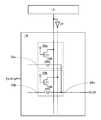
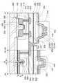
도 14에, 본 발명의 일 실시 형태에 따른 PLD의 단면 구조의 일례를 나타낸다. 도 14에서는, 산화물 반도체 막에 채널 형성 영역을 포함하는 트랜지스터(21)가, 단결정의 실리콘 기판에 채널 형성 영역을 포함하는 트랜지스터(22) 위에 형성되어 있다.14 shows an example of a cross-sectional structure of a PLD according to an embodiment of the present invention. In Fig. 14, a
트랜지스터(22)는 비정질, 미결정, 다결정 또는 단결정 상태의 실리콘, 게르마늄 등의 반도체 막을 활성층으로서 포함할 수도 있다. 혹은, 트랜지스터(22)는 산화물 반도체 막에 채널 형성 영역을 포함하고 있어도 된다. 각각의 트랜지스터가 산화물 반도체 막에 채널 형성 영역을 포함하고 있는 경우, 트랜지스터(21)는 트랜지스터(22) 상에 적층되지 않아도 되고, 트랜지스터(21, 22)가 동일한 층에 형성되어 있어도 된다.The
박막의 실리콘을 사용해서 트랜지스터(22)를 형성하는 경우, 플라즈마 인헨스드 CVD법 등의 기상 성장법 혹은 스퍼터링법에 의해 제작된 비정질 실리콘, 비정질 실리콘을 레이저 어닐링 등의 처리에 의해 결정화하여 얻어지는 다결정 실리콘, 단결정 실리콘 웨이퍼에 수소 이온 등을 주입해서 이 실리콘 웨이퍼의 표층부를 박리하여 얻어지는 단결정 실리콘 중 임의의 것이 사용될 수 있다.When the
트랜지스터(22)가 형성되는 반도체 기판(400)은, 예를 들어 n형 또는 p형의 실리콘 기판, 게르마늄 기판, 실리콘 게르마늄 기판 또는 화합물 반도체 기판(예를 들어, GaAs 기판, InP 기판, GaN 기판, SiC 기판, GaP 기판, GaInAsP 기판 또는 ZnSe 기판)을 사용할 수 있다. 도 14에서는, n형의 도전성을 갖는 단결정 실리콘 기판을 사용한다.The
트랜지스터(22)는 소자 분리용 절연막(401)에 의해 다른 트랜지스터로부터 전기적으로 분리되고 있다. 소자 분리용 절연막(401)의 형성에는, 선택 산화법(LOCOS(local oxidation of silicon)법), 트렌치 분리법 등을 사용할 수 있다.The
구체적으로, 트랜지스터(22)는 반도체 기판(400)에 형성된, 소스 영역 및 드레인 영역으로서 기능하는 불순물 영역(402 및 403)과, 게이트 전극(404)과, 반도체 기판(400)과 게이트 전극(404)의 사이에 제공된 게이트 절연막(405)을 포함한다. 게이트 전극(404)은, 게이트 전극(404)과 채널 형성 영역의 사이에 게이트 절연막(405)을 끼우고, 불순물 영역(402)과 불순물 영역(403)의 사이에 형성되는 채널 형성 영역과 중첩된다.Specifically, the
트랜지스터(22) 위에는 절연막(409)이 제공된다. 절연막(409)에는 개구부가 형성된다. 상기 개구부에는, 불순물 영역(402, 403)에 각각 접하는 배선(410, 411)과, 게이트 전극(404)에 전기적으로 접속되고 있는 배선(412)이 형성된다.An insulating
배선(410)은 절연막(409) 위에 형성된 배선(415)에 전기적으로 접속되어 있다. 배선(411, 412)은 절연막(409) 위에 형성된 배선(416)에 전기적으로 접속되어 있다. 배선(412)은, 절연막(409) 위에 형성된 배선(417)에 전기적으로 접속되고 있다.The
배선(415 내지 417) 위에는, 절연막(420) 및 절연막(440)이 순서대로 적층된다. 절연막(420) 및 절연막(440)에는 개구부가 형성되어 있다. 상기 개구부에, 배선(417)에 전기적으로 접속되는 배선(421)이 형성된다.On the
도 14에서는, 절연막(440) 위에 트랜지스터(21)가 형성된다.In FIG. 14, a
트랜지스터(21)는 절연막(440) 위에 산화물 반도체를 포함하는 반도체 막(430)과, 반도체 막(430) 위에 배치되고, 소스 전극 및 드레인 전극으로서 기능하는 도전막(432 및 433)과, 반도체 막(430) 및 도전막(432 및 433) 위의 게이트 절연막(431)과, 게이트 절연막(431) 위에 위치하고, 도전막(432)과 도전막(433)의 사이에서 반도체 막(430)과 중첩하는 게이트 전극(434)을 포함한다.The
트랜지스터(21) 위에 절연막(441) 및 절연막(442)이 순서대로 적층된다. 절연막(441, 442)에는 개구부가 형성되어 있다. 상기 개구부에서 게이트 전극(434)에 접하는 도전막(443)이 절연막(441) 위에 제공된다.On the
도 14에서, 트랜지스터(21)는 게이트 전극(434)을 반도체 막(430)의 적어도 한 측에 포함한다. 또는, 트랜지스터(21)는 반도체 막(430)을 사이에 끼워서 존재하는 한 쌍의 게이트 전극을 포함하고 있어도 된다.In FIG. 14, the
트랜지스터(21)가, 반도체 막(430)을 사이에 끼워서 존재하는 한 쌍의 게이트 전극을 포함하는 경우, 한쪽의 게이트 전극에는 도통 상태 또는 비도통 상태를 제어하기 위한 신호가 부여되고, 다른 쪽의 게이트 전극에는 전위가 다른 요소로부터 부여되고 있어도 된다. 이 경우, 한 쌍의 게이트 전극에 동일한 레벨의 전위가 부여되고 있어도 되고, 다른 쪽의 게이트 전극에만 접지 전위 등의 고정 전위가 부여되고 있어도 된다. 다른 쪽의 게이트 전극에 부여하는 전위의 레벨을 제어함으로써, 트랜지스터의 역치 전압을 제어할 수 있다.When the
도 14에서는, 트랜지스터(21)는, 하나의 게이트 전극(434)에 대응하는 하나의 채널 형성 영역이 제공되는 싱글 게이트 구조를 가진다. 그러나, 트랜지스터(21)는, 서로 전기적으로 접속된 복수의 게이트 전극을 제공함으로써, 하나의 활성층에 채널 형성 영역이 복수 형성되는 멀티 게이트 구조이어도 된다.In FIG. 14, the
<반도체 막><Semiconductor membrane>
전자 공여체(도너)가 되는 수분 또는 수소 등의 불순물이 저감되고, 산소 결손이 저감됨으로써 얻어지는 고순도화된 산화물 반도체(순도화된 산화물 반도체)는 진성(i형) 반도체 또는 실질적으로 진성 반도체이다. 그로 인해, 고순도화된 산화물 반도체 막에 채널 형성 영역을 포함하는 트랜지스터는, 오프 전류가 현저하게 작고, 신뢰성이 높다.The highly purified oxide semiconductor (purified oxide semiconductor) obtained by reducing impurities such as moisture or hydrogen to become an electron donor (donor) and reducing oxygen deficiency is an intrinsic (i-type) semiconductor or substantially an intrinsic semiconductor. Therefore, the off current is remarkably small and the reliability of the transistor including the channel formation region in the highly purified oxide semiconductor film is high.
구체적으로, 고순도화된 산화물 반도체 막에 채널 형성 영역을 포함하는 트랜지스터의 오프 전류가 작은 것은 다양한 실험에 의해 증명할 수 있다. 예를 들어, 채널 폭이 1×106μm이고 채널 길이가 10μm인 소자의 경우에도, 소스 전극과 드레인 전극 간의 전압(드레인 전압)이 1 내지 10V인 범위에서, 오프 전류가 반도체 파라미터 애널라이저의 측정 한계 이하, 즉 1×10-13A 이하일 수 있다. 이 경우, 트랜지스터의 채널 폭에 규격화된 오프 전류는 100zA/μm 이하인 것을 안다. 또한, 용량 소자와 트랜지스터를 서로 접속하고, 용량 소자에 유입하거나 용량 소자로부터 유출하는 전하를 당해 트랜지스터에 의해 제어하는 회로를 사용하여, 오프 전류의 측정을 행했다. 당해 측정에서는, 고순도화된 산화물 반도체 막을 상기 트랜지스터의 채널 형성 영역에 사용하고, 용량 소자의 단위 시간 당의 전하량의 변화로부터 당해 트랜지스터의 오프 전류를 측정했다. 그 결과, 트랜지스터의 소스 전극과 드레인 전극 간의 전압이 3V의 경우에, 수 십 yA/μm의 작은 오프 전류가 얻어지는 것을 알았다. 따라서, 고순도화된 산화물 반도체 막을 채널 형성 영역에 포함하는 트랜지스터는, 오프 전류가 결정 실리콘 트랜지스터에 비해서 현저하게 작다.Specifically, a small off current of a transistor including a channel formation region in a highly purified oxide semiconductor film can be proved by various experiments. For example, even in a device having a channel width of 1×106 μm and a channel length of 10 μm, the off-current is measured by the semiconductor parameter analyzer in a range of 1 to 10 V between the source electrode and the drain electrode (drain voltage). It may be below the limit, that is, 1×10-13 A or less. In this case, it is found that the off current normalized to the channel width of the transistor is 100 zA/μm or less. Further, the off-current was measured using a circuit in which the capacitors and transistors are connected to each other, and the charges flowing into or out of the capacitors are controlled by the transistors. In this measurement, a highly purified oxide semiconductor film was used for the channel formation region of the transistor, and the off-state current of the transistor was measured from the change in the amount of charge per unit time of the capacitor element. As a result, it was found that when the voltage between the source electrode and the drain electrode of the transistor was 3 V, a small off current of several tens of yA/μm was obtained. Therefore, the off current of the transistor including the highly purified oxide semiconductor film in the channel formation region is significantly smaller than that of the crystalline silicon transistor.
달리 특정하지 않는 한, 본 명세서에서, n채널형 트랜지스터의 오프 전류는, 소스의 전위를 기준으로 사용하는 경우에 게이트의 전위를 0V 이하로 하면서, 드레인의 전위를 소스의 전위 또는 게이트의 전위보다 높게 할 때의 소스와 드레인 사이를 흐르는 전류이다. 혹은, 본 명세서에서, p채널형 트랜지스터의 오프 전류는, 소스의 전위를 기준으로 사용하는 경우에 게이트의 전위를 0V 이하로 하면서, 드레인의 전위를 소스의 전위 또는 게이트의 전위보다 낮게 할 때의 소스와 드레인 사이를 흐르는 전류이다.Unless otherwise specified, in the present specification, the off-state current of the n-channel transistor is set to the potential of the gate to be 0 V or less when used based on the potential of the source, and the potential of the drain is greater than the potential of the source or the potential of the gate. It is the current that flows between the source and drain at the height. Alternatively, in the present specification, when the off-state current of the p-channel transistor is used as a reference to the potential of the source, the potential of the drain is set to 0 V or less while the potential of the drain is lower than the potential of the source or the potential of the gate. This is the current flowing between the source and drain.
반도체 막으로서 산화물 반도체 막을 사용하는 경우, 산화물 반도체로서는 적어도 인듐(In) 혹은 아연(Zn)을 포함하는 것이 바람직하다. 해당 산화물 반도체 막을 포함하는 트랜지스터의 전기적 특성의 변동을 저감시키기 위한 스테빌라이저로서, 산화물 반도체는 In 및 Zn 외에 갈륨(Ga)을 포함하는 것이 바람직하다. 스테빌라이저로서 주석(Sn)을 포함하는 것이 바람직하다. 스테빌라이저로서 하프늄(Hf)을 포함하는 것이 바람직하다. 스테빌라이저로서 알루미늄(Al)을 포함하는 것이 바람직하다. 스테빌라이저로서 지르코늄(Zr)을 포함하는 것이 바람직하다.When an oxide semiconductor film is used as the semiconductor film, it is preferable that the oxide semiconductor contains at least indium (In) or zinc (Zn). As a stabilizer for reducing fluctuations in electrical characteristics of the transistor including the oxide semiconductor film, the oxide semiconductor preferably contains gallium (Ga) in addition to In and Zn. It is preferable to include tin (Sn) as a stabilizer. It is preferred to include hafnium (Hf) as a stabilizer. It is preferable to include aluminum (Al) as a stabilizer. It is preferred to include zirconium (Zr) as a stabilizer.
산화물 반도체 중에서도, In-Ga-Zn계 산화물, In-Sn-Zn계 산화물 등은, 탄화실리콘, 질화갈륨 또는 산화갈륨과는 상이하게, 스퍼터링법이나 습식법에 의해 전기적 특성의 우수한 트랜지스터를 제작하는 것이 가능하기 때문에, 양산성이 우수한 이점이 있다. 또한, 탄화실리콘, 질화갈륨 또는 산화갈륨과는 상이하게, In-Ga-Zn계 산화물을 사용하면, 유리 기판 위에 전기적 특성의 우수한 트랜지스터를 제작하는 것이 가능하다. 또한, 기판의 대형화에도 대응이 가능하다.Among oxide semiconductors, In-Ga-Zn-based oxides, In-Sn-Zn-based oxides, and the like, unlike silicon carbide, gallium nitride, or gallium oxide, it is preferable to manufacture a transistor having excellent electrical properties by sputtering or wet method. Since it is possible, there is an advantage of excellent mass productivity. In addition, differently from silicon carbide, gallium nitride or gallium oxide, it is possible to manufacture a transistor having excellent electrical properties on a glass substrate by using an In-Ga-Zn-based oxide. In addition, it is possible to cope with the enlargement of the substrate.
다른 스테빌라이저로서, 란탄(La), 세륨(Ce), 프라세오디뮴(Pr), 네오디뮴(Nd), 사마륨(Sm), 유로퓸(Eu), 가돌리늄(Gd), 테르븀(Tb), 디스프로슘(Dy), 홀뮴(Ho), 에르븀(Er), 툴륨(Tm), 이테르븀(Yb) 또는 루테튬(Lu) 중 1종 이상의 란타노이드를 포함하고 있어도 된다.Other stabilizers include: lanthanum (La), cerium (Ce), praseodymium (Pr), neodymium (Nd), samarium (Sm), europium (Eu), gadolinium (Gd), terbium (Tb), dysprosium (Dy), It may contain one or more lanthanoids among holmium (Ho), erbium (Er), thulium (Tm), ytterbium (Yb), or lutetium (Lu).
예를 들어, 산화물 반도체로서, 산화인듐, 산화갈륨, 산화주석, 산화아연, In-Zn계 산화물, Sn-Zn계 산화물, Al-Zn계 산화물, Zn-Mg계 산화물, Sn-Mg계 산화물, In-Mg계 산화물, In-Ga계 산화물, In-Ga-Zn계 산화물(IGZO라고도 표기한다), In-Al-Zn계 산화물, In-Sn-Zn계 산화물, Sn-Ga-Zn계 산화물, Al-Ga-Zn계 산화물, Sn-Al-Zn계 산화물, In-Hf-Zn계 산화물, In-La-Zn계 산화물, In-Pr-Zn계 산화물, In-Nd-Zn계 산화물, In-Sm-Zn계 산화물, In-Eu-Zn계 산화물, In-Gd-Zn계 산화물, In-Tb-Zn계 산화물, In-Dy-Zn계 산화물, In-Ho-Zn계 산화물, In-Er-Zn계 산화물, In-Tm-Zn계 산화물, In-Yb-Zn계 산화물, In-Lu-Zn계 산화물, In-Sn-Ga-Zn계 산화물, In-Hf-Ga-Zn계 산화물, In-Al-Ga-Zn계 산화물, In-Sn-Al-Zn계 산화물, In-Sn-Hf-Zn계 산화물 또는 In-Hf-Al-Zn계 산화물을 사용할 수 있다.For example, as an oxide semiconductor, indium oxide, gallium oxide, tin oxide, zinc oxide, In-Zn-based oxide, Sn-Zn-based oxide, Al-Zn-based oxide, Zn-Mg-based oxide, Sn-Mg-based oxide, In-Mg-based oxide, In-Ga-based oxide, In-Ga-Zn-based oxide (also referred to as IGZO), In-Al-Zn-based oxide, In-Sn-Zn-based oxide, Sn-Ga-Zn-based oxide, Al-Ga-Zn-based oxide, Sn-Al-Zn-based oxide, In-Hf-Zn-based oxide, In-La-Zn-based oxide, In-Pr-Zn-based oxide, In-Nd-Zn-based oxide, In- Sm-Zn-based oxide, In-Eu-Zn-based oxide, In-Gd-Zn-based oxide, In-Tb-Zn-based oxide, In-Dy-Zn-based oxide, In-Ho-Zn-based oxide, In-Er- Zn-based oxide, In-Tm-Zn-based oxide, In-Yb-Zn-based oxide, In-Lu-Zn-based oxide, In-Sn-Ga-Zn-based oxide, In-Hf-Ga-Zn-based oxide, In- Al-Ga-Zn-based oxide, In-Sn-Al-Zn-based oxide, In-Sn-Hf-Zn-based oxide, or In-Hf-Al-Zn-based oxide can be used.
예를 들어, In-Ga-Zn계 산화물은, In과, Ga와, Zn을 포함하는 산화물을 의미하며, In과 Ga와 Zn의 비율은 제한하지 않는다. 또한, In-Ga-Zn계 산화물은 In과 Ga와 Zn이외의 금속 원소를 포함하고 있어도 된다. In-Ga-Zn계 산화물은, 전계가 인가되지 않을 경우의 저항이 충분히 높아서, 오프 전류를 충분히 작게 하는 것이 가능하다. 또한, In-Ga-Zn계 산화물은 이동도도 높다.For example, the In-Ga-Zn-based oxide means an oxide containing In, Ga, and Zn, and the ratio of In, Ga, and Zn is not limited. Further, the In-Ga-Zn-based oxide may contain metal elements other than In, Ga, and Zn. The In-Ga-Zn-based oxide has a sufficiently high resistance when no electric field is applied, and it is possible to make the off current sufficiently small. In addition, In-Ga-Zn-based oxides also have high mobility.
예를 들어, In:Ga:Zn=1:1:1(=1/3:1/3:1/3) 혹은 In:Ga:Zn=2:2:1(=2/5:2/5:1/5)의 원자수비의 In-Ga-Zn계 산화물이나, 상기 조성의 근방의 조성을 가지는 산화물을 사용할 수 있다. 혹은, In:Sn:Zn=1:1:1(=1/3:1/3:1/3), In:Sn:Zn=2:1:3(=1/3:1/6:1/2) 혹은 In:Sn:Zn=2:1:5(=1/4:1/8:5/8)의 원자수비의 In-Sn-Zn계 산화물이나 상기 조성의 근방의 조성을 가지는 산화물을 사용하는 것이 바람직하다.For example, In:Ga:Zn=1:1:1(=1/3:1/3:1/3) or In:Ga:Zn=2:2:1(=2/5:2/5 An In-Ga-Zn-based oxide having an atomic ratio of :1/5) or an oxide having a composition in the vicinity of the above composition can be used. Or, In:Sn:Zn=1:1:1 (=1/3:1/3:1/3), In:Sn:Zn=2:1:3 (=1/3:1/6:1 /2) or In:Sn:Zn=2:1:5 (=1/4:1/8:5/8), an atomic ratio of In-Sn-Zn oxide or an oxide having a composition near the composition It is preferred to use.
예를 들어, In-Sn-Zn계 산화물에서는 비교적 용이하게 높은 이동도가 얻어진다. 그러나, In-Ga-Zn계 산화물에서도, 벌크 내의 결함 밀도를 저감함으로써 이동도를 증가시킬 수 있다.For example, high mobility can be obtained relatively easily with In-Sn-Zn-based oxides. However, even in the In-Ga-Zn-based oxide, the mobility can be increased by reducing the defect density in the bulk.
이하에서는, 산화물 반도체 막의 구조에 대해서 설명한다.Hereinafter, the structure of the oxide semiconductor film will be described.
산화물 반도체 막은, 단결정 산화물 반도체 막과 비단결정 산화물 반도체 막으로 크게 구별된다. 비단결정 산화물 반도체 막은, 비정질 산화물 반도체 막, 미결정 산화물 반도체 막, 다결정 산화물 반도체 막, CAAC-OS(c-axis aligned crystalline oxide semiconductor)막 등을 의미한다.The oxide semiconductor film is roughly divided into a single crystal oxide semiconductor film and a non-single crystal oxide semiconductor film. The non-single-crystal oxide semiconductor film means an amorphous oxide semiconductor film, a microcrystalline oxide semiconductor film, a polycrystalline oxide semiconductor film, a c-axis aligned crystalline oxide semiconductor (CAAC-OS) film, or the like.
비정질 산화물 반도체 막은 원자 배열이 불규칙해서, 결정 성분을 갖지 않는다. 미소 영역에서도 결정부를 갖지 않고, 막 전체가 비정질 구조인 산화물 반도체 막이 비정질 산화물 반도체 막의 전형적인 예이다.The amorphous oxide semiconductor film has an irregular atomic arrangement, and thus has no crystalline component. An oxide semiconductor film having no crystal part in the micro region and having an amorphous structure as a whole is a typical example of the amorphous oxide semiconductor film.
미결정 산화물 반도체 막은, 예를 들어 1nm 이상 10nm 미만의 크기의 미결정(나노 결정이라고도 말한다)을 포함한다. 따라서, 미결정 산화물 반도체 막은, 비정질 산화물 반도체 막보다 원자 배열의 규칙성이 높다. 그로 인해, 미결정 산화물 반도체 막은, 비정질 산화물 반도체 막보다 결함 준위 밀도가 낮다.The microcrystalline oxide semiconductor film contains, for example, microcrystals (also referred to as nanocrystals) having a size of 1 nm or more and less than 10 nm. Therefore, the microcrystalline oxide semiconductor film has a higher degree of atomic order than the amorphous oxide semiconductor film. Therefore, the defect level density of the microcrystalline oxide semiconductor film is lower than that of the amorphous oxide semiconductor film.
CAAC-OS막은, 복수의 결정부를 포함하는 산화물 반도체 막의 하나이며, 대부분의 결정부는 각각 한 변이 100nm 미만인 입방체 내에 수용되는 크기이다. 따라서, CAAC-OS막에 포함되는 결정부가 한 변이 10nm 미만, 5nm 미만 또는 3nm 미만인 입방체 내에 수용되는 크기의 경우도 있다. CAAC-OS막은, 미결정 산화물 반도체 막보다 결함 준위 밀도가 낮다. 이하, CAAC-OS막에 대해서 상세한 설명을 행한다.The CAAC-OS film is one of oxide semiconductor films including a plurality of crystal parts, and most of the crystal parts are sized to be accommodated in a cube whose side is less than 100 nm. Therefore, there are cases where the crystal part included in the CAAC-OS film is accommodated in a cube whose side is less than 10 nm, less than 5 nm, or less than 3 nm. The CAAC-OS film has a lower defect level density than the microcrystalline oxide semiconductor film. Hereinafter, the CAAC-OS film will be described in detail.
CAAC-OS막의 투과형 전자 현미경(TEM) 상에서는, 결정부 사이의 경계, 즉 결정립계가 명확하게 확인되지 않는다. 그로 인해, CAAC-OS막에서는, 결정립계에 기인하는 전자 이동도의 저하가 일어나기 어렵다고 할 수 있다.On the transmission electron microscope (TEM) of the CAAC-OS film, a boundary between crystal parts, that is, a grain boundary is not clearly identified. For this reason, it can be said that it is difficult for the CAAC-OS film to lower the electron mobility due to grain boundaries.
CAAC-OS막을, 시료면과 대략 평행한 방향에서 관찰한 TEM 상(단면 TEM 상)에 의하면, 결정부에서 금속 원자가 층상으로 배열되어 있다. 금속 원자의 각 층은, CAAC-OS막을 형성하는 면(이하, CAAC-OS막을 형성하는 면을 형성면이라고도 한다) 또는 CAAC-OS막의 상면을 반영한 형상이며, CAAC-OS막의 형성면 또는 상면과 평행하게 배열한다.According to the TEM image (cross-sectional TEM image) of the CAAC-OS film observed in a direction substantially parallel to the sample surface, metal atoms are arranged in layers in the crystal part. Each layer of the metal atom is a surface that forms a CAAC-OS film (hereinafter, also referred to as a surface that forms a CAAC-OS film) or a shape that reflects the top surface of the CAAC-OS film, and the surface or surface of the CAAC-OS film. Arrange in parallel.
본 명세서에서, "평행"이라는 용어는, 2개의 직선 사이에 형성되는 각도가 -10 내지 10°인 것을 나타내고, 따라서, 상기 각도가 -5 내지 5°인 경우도 포함한다. 또한, "수직"이라는 용어는, 2개의 직선 사이에 형성되는 각도가 80 내지 100°인 것을 나타내고, 따라서, 85 내지 95°의 경우도 포함한다.In the present specification, the term "parallel" indicates that the angle formed between two straight lines is -10 to 10°, and therefore, also includes the case where the angle is -5 to 5°. In addition, the term "vertical" indicates that the angle formed between the two straight lines is 80 to 100°, and thus includes the case of 85 to 95°.
한편, 시료면과 대략 수직인 방향에서 관찰되는 CAAC-OS막의 TEM 상(평면 TEM 상)에 의하면, 결정부에서 금속 원자가 삼각 형상 또는 육각형 형상으로 배열하고 있다. 그러나, 다른 결정부 간에는, 금속 원자의 배열에 규칙성은 보이지 않는다.On the other hand, according to the TEM image (planar TEM image) of the CAAC-OS film observed in a direction substantially perpendicular to the sample surface, metal atoms are arranged in a triangular or hexagonal shape in the crystal part. However, there is no regularity in the arrangement of metal atoms between different crystal parts.
단면 TEM 상 및 평면 TEM 상의 결과로부터, CAAC-OS막의 결정부에는 배향성이 발견된다.From the results of the cross-sectional TEM image and the planar TEM image, orientation is found in the crystal part of the CAAC-OS film.
CAAC-OS막에 대하여, X선 회절(XRD) 장치를 사용해서 구조 해석을 행한다. 예를 들어, InGaZnO4의 결정을 포함하는 CAAC-OS막의 면외(out-of-plane)법에 의한 해석 시에는, 회절각(2θ)이 31° 근방인 때에 피크가 나타날 경우가 종종 있다. 이 피크는, InGaZnO4의 결정의 (009)면으로부터 유도되는데, 이것은, CAAC-OS막의 결정이 c축 배향성을 갖고, c축이 CAAC-OS막의 형성면 또는 상면에 대략 수직인 방향으로 배향하고 있음을 나타낸다.The CAAC-OS film is subjected to structural analysis using an X-ray diffraction (XRD) device. For example, during analysis by an out-of-plane method of a CAAC-OS film containing InGaZnO4 crystals, peaks often appear when the diffraction angle (2θ) is around 31°. This peak is derived from the (009) plane of the crystal of InGaZnO4, which means that the crystal of the CAAC-OS film has c-axis orientation, and the c-axis is oriented in a direction substantially perpendicular to the formation surface or top surface of the CAAC-OS film. It is present.
한편, CAAC-OS막에 대하여, c축에 대략 수직인 방향으로 시료에 X선을 입사시키는 면내(in-plane)법에 의한 해석 시에는, 2θ가 56° 근방일 때에 피크가 나타날 경우가 종종 있다. 이 피크는 InGaZnO4 결정의 (110)면으로부터 유도된다. 여기서, 2θ를 56° 근방에 고정하고, 시료면의 법선 벡터를 축(φ축)으로 하여 시료를 회전시키면서 분석(φ 스캔)을 행한다. 시료가 InGaZnO4의 단결정 산화물 반도체 막인 경우, 6개의 피크가 나타난다. 이 6개의 피크는 (110)면과 등가인 결정면으로부터 유도된다. 이에 대해, CAAC-OS막의 경우에는, 2θ를 56° 근방에 고정해서 φ 스캔을 행한 경우에도, 명료한 피크가 관찰되지 않는다.On the other hand, in the case of analysis by an in-plane method in which X-rays are incident on a sample in a direction substantially perpendicular to the c-axis with respect to the CAAC-OS film, peaks often appear when 2θ is around 56°. have. This peak is derived from the (110) plane of the InGaZnO4 crystal. Here, 2θ is fixed around 56°, and analysis (φ scan) is performed while rotating the sample using the normal vector of the sample surface as the axis (φ axis). When the sample is an InGaZnO4 single crystal oxide semiconductor film, six peaks appear. These six peaks are derived from a crystal plane equivalent to the (110) plane. On the other hand, in the case of the CAAC-OS film, a clear peak is not observed even when φ scan is performed by fixing 2θ at around 56°.
이상의 결과에 따르면, c축 배향성을 갖는 CAAC-OS막에서는, a축 및 b축의 배향은 결정부 간에 상이하지만, c축은 형성면의 법선 벡터 또는 상면의 법선 벡터에 평행한 방향으로 배향된다. 따라서, 층상으로 배열하고, 단면 TEM 상에서 관찰되는 금속 원자의 각 층은, 결정의 ab면에 평행한 면에 대응한다.According to the above results, in the CAAC-OS film having c-axis orientation, the orientation of the a-axis and the b-axis is different between the crystal parts, but the c-axis is oriented in a direction parallel to the normal vector of the forming surface or the normal vector of the upper surface. Therefore, each layer of the metal atoms arranged in layers and observed on the cross-section TEM corresponds to a surface parallel to the ab surface of the crystal.
결정부는, CAAC-OS막의 성막과 함께, 또는 가열 처리 등의 결정화 처리를 통해서 형성된다. 상술한 바와 같이, 결정의 c축은 형성면의 법선 벡터 또는 상면의 법선 벡터에 평행한 방향으로 정렬된다. 따라서, 예를 들어 CAAC-OS막의 형상을 에칭 등에 의해 변화시킨 경우, c축이 CAAC-OS막의 형성면의 법선 벡터 또는 상면의 법선 벡터와 반드시 평행하지 않을 수도 있다.The crystal part is formed together with the film formation of the CAAC-OS film or through a crystallization process such as heat treatment. As described above, the c-axis of the crystal is aligned in a direction parallel to the normal vector of the forming surface or the normal vector of the upper surface. Therefore, for example, when the shape of the CAAC-OS film is changed by etching or the like, the c-axis may not necessarily be parallel to the normal vector on the formation surface of the CAAC-OS film or the normal vector on the top surface.
또한, CAAC-OS막 내의 결정화도가 반드시 균일하지 않아도 된다. 예를 들어, CAAC-OS막을 형성하는 결정 성장이 막의 상면 근방으로부터 발생하는 경우, 상면 근방의 결정화도가 형성면 근방의 결정화도보다 높을 경우가 있다. 또한, CAAC-OS막에 불순물을 첨가하는 경우, 불순물이 첨가된 영역의 결정화도가 변화하고, CAAC-OS막의 결정화도가 영역에 따라 달라진다.Further, the crystallinity in the CAAC-OS film does not necessarily have to be uniform. For example, when the crystal growth forming the CAAC-OS film occurs from the vicinity of the top surface of the film, the crystallinity of the top surface may be higher than the crystallinity of the formation surface. In addition, when an impurity is added to the CAAC-OS film, the crystallinity of the region to which the impurity is added changes, and the crystallinity of the CAAC-OS film varies depending on the region.
InGaZnO4의 결정을 갖는 CAAC-OS막이 면외법에 의한 해석되는 경우, 2θ의 31° 근방의 피크 이외에, 2θ의 피크가 36° 근방에도 드러날 경우가 있다. 2θ의 36° 근방의 피크는, CAAC-OS막의 일부에 c축 배향성을 갖지 않은 결정이 포함되는 것을 나타내고 있다. CAAC-OS막은, 2θ의 피크가 31° 근방에 나타내고, 2θ의 피크가 36° 근방에 나타나지 않는 것이 바람직하다.When the CAAC-OS film having InGaZnO4 crystals is analyzed by an out-of-plane method, a peak of 2θ may also appear in the vicinity of 36° in addition to a peak near 31° of 2θ. The peak at around 36° of 2θ indicates that a crystal having no c-axis orientation is included in a part of the CAAC-OS film. In the CAAC-OS film, it is preferable that a peak of 2θ appears near 31° and a peak of 2θ does not appear near 36°.
CAAC-OS막을 포함하는 트랜지스터에서는, 가시광이나 자외광의 조사에 의한 트랜지스터의 전기적 특성의 변동이 작다. 따라서, 당해 트랜지스터는 신뢰성이 높다.In a transistor including a CAAC-OS film, variations in electrical characteristics of the transistor due to irradiation with visible light or ultraviolet light are small. Therefore, the transistor is highly reliable.
산화물 반도체 막은, 예를 들어 비정질 산화물 반도체 막, 미결정 산화물 반도체 막, CAAC-OS막 중 2종 이상을 포함하는 적층막이어도 된다.The oxide semiconductor film may be, for example, an amorphous oxide semiconductor film, a microcrystalline oxide semiconductor film, or a laminated film containing two or more of CAAC-OS films.
CAAC-OS막은, 예를 들어 다결정 금속 산화물 타깃을 사용하는 스퍼터링법에 의해 성막한다. 당해 타깃에 이온이 충돌하면, 타깃에 포함되는 결정 영역이 a-b면을 따라 타깃으로부터 분리되고, a-b면에 평행한 면을 가지는 스퍼터링 입자(평판 형상 또는 펠릿 형상의 스퍼터링 입자)가 타깃으로부터 박리되는 경우가 있다. 이 경우, 당해 평판 형상 또는 펠릿 형상의 스퍼터링 입자가 결정 상태를 유지한 채 기판에 도달함으로써, CAAC-OS막을 성막할 수 있다.The CAAC-OS film is formed by a sputtering method using, for example, a polycrystalline metal oxide target. When ions collide with the target, crystal regions included in the target are separated from the target along the ab surface, and sputtering particles (flat or pellet-shaped sputtering particles) parallel to the ab surface are peeled from the target. There is. In this case, the CAAC-OS film can be formed by depositing the flat or pellet-shaped sputtering particles to the substrate while maintaining the crystal state.
CAAC-OS막을 성막하기 위해서, 이하의 조건을 적용하는 것이 바람직하다.In order to form a CAAC-OS film, it is preferable to apply the following conditions.
성막 시에 CAAC-OS막으로의 불순물 혼입량을 저감함으로써, 불순물에 의해 결정 상태가 무너지는 것을 억제할 수 있다. 예를 들어, 처리실 내에 존재하는 불순물 농도(예를 들어, 수소, 물, 이산화탄소 또는 질소)를 저감하면 된다. 또한, 성막 가스 중의 불순물 농도를 저감하면 된다. 구체적으로는, 노점이 -80℃ 이하, 바람직하게는 -100℃ 이하인 성막 가스를 사용한다.By reducing the amount of impurities incorporated into the CAAC-OS film during film formation, it is possible to suppress the collapse of the crystal state due to impurities. For example, it is sufficient to reduce the impurity concentration (for example, hydrogen, water, carbon dioxide or nitrogen) present in the treatment chamber. Moreover, it is sufficient to reduce the impurity concentration in the film forming gas. Specifically, a deposition gas having a dew point of -80°C or lower, preferably -100°C or lower, is used.
성막 시의 기판 가열 온도를 높임으로써, 스퍼터링 입자가 기판에 도달한 후에 스퍼터링 입자의 마이그레이션이 일어난다. 구체적으로는, 기판 가열 온도를 100℃ 이상 740℃ 이하, 바람직하게는 200℃ 이상 500℃ 이하로 해서 성막한다. 성막 시의 기판 가열 온도를 높임으로써, 평판 형상 또는 펠릿 형상의 스퍼터링 입자가 기판에 도달한 경우, 기판 상에서 마이그레이션이 일어나서, 스퍼터링 입자의 평평한 면이 기판에 부착된다.By increasing the substrate heating temperature during film formation, migration of sputtering particles occurs after the sputtering particles reach the substrate. Specifically, the film is formed by setting the substrate heating temperature to 100°C or more and 740°C or less, preferably 200°C or more and 500°C or less. When the substrate heating temperature at the time of film formation is increased, when flat or pellet-shaped sputtering particles reach the substrate, migration occurs on the substrate, and the flat surface of the sputtering particles adheres to the substrate.
또한, 성막 가스 중의 산소 비율을 높이고, 전력을 최적화함으로써 성막 시의 플라즈마 손상을 경감하는 것이 바람직하다. 성막 가스 중의 산소의 비율은, 30 체적% 이상, 바람직하게는 100체적%로 한다.In addition, it is desirable to reduce the plasma damage during film formation by increasing the oxygen ratio in the film forming gas and optimizing electric power. The proportion of oxygen in the film forming gas is 30 volume% or more, preferably 100 volume%.
타깃의 일례로서, In-Ga-Zn계 산화물 타깃에 대해서 이하에 설명한다.As an example of the target, an In-Ga-Zn-based oxide target will be described below.
InOX 분말, GaOY 분말 및 ZnOZ 분말을 미리 정해진 mol비로 혼합하고, 가압 처리 후, 1000 내지 1500℃의 온도에서 가열 처리를 함으로써 다결정 In-Ga-Zn계 산화물 타깃이 만들어진다. X, Y 및 Z는 각각 임의의 양수이다. 여기서, InOX 분말, GaOY 분말 및 ZnOZ 분말의 미리 정해진 mol비는, 예를 들어 2:2:1, 8:4:3, 3:1:1, 1:1:1, 4:2:3 또는 3:1:2이다. 분말의 종류 및 혼합하는 분말의 mol비는, 제작하는 타깃에 따라 적절히 변경하면 된다.A polycrystalline In-Ga-Zn-based oxide target is made by mixing InOX powder, GaOY powder, and ZnOZ powder at a predetermined mol ratio, followed by heat treatment at a temperature of 1000 to 1500°C after pressurization treatment. X, Y and Z are each positive numbers. Here, the predetermined mol ratios of InOX powder, GaOY powder and ZnOZ powder are, for example, 2:2:1, 8:4:3, 3:1:1, 1:1:1, 4:2 :3 or 3:1:2. The type of powder and the mol ratio of the powder to be mixed may be appropriately changed depending on the target to be produced.
알칼리 금속은 산화물 반도체에 포함되는 원소가 아니기 때문에, 불순물이다. 알칼리 토금속도, 산화물 반도체에 알칼리 토금속이 포함되지 않는 경우에는 불순물이다. 특히, 알칼리 금속 Na는, 산화물 반도체 막에 접하는 절연막이 산화물이고, Na가 당해 절연막 내에 확산해서 Na+이 된다. 또한, Na는, 산화물 반도체 막 내에서, 산화물 반도체에 포함되는 금속과 산소의 결합을 절단하거나, 혼입한다. 그 결과, 예를 들어 역치 전압이 음의 방향으로 시프트하는 것에 의한 트랜지스터의 노멀리 온 상태(normally on state), 또는 이동도의 저하 등의 트랜지스터의 전기적 특성의 열화가 발생한다. 구체적으로, 2차 이온 질량 분석법에 의한 Na 농도의 측정값은, 5×10¹⁶/cm3 이하, 바람직하게는 1×10¹⁶/cm3 이하, 더욱 바람직하게는 1×10¹⁵/cm3 이하로 하면 된다. 마찬가지로, Li 농도의 측정값은, 5×10¹⁵/cm3 이하, 바람직하게는 1×10¹⁵/cm3 이하로 하면 된다. 마찬가지로, K 농도의 측정값은, 5×10¹⁵/cm3 이하, 바람직하게는 1×10¹⁵/cm3 이하로 하면 된다.Since the alkali metal is not an element included in the oxide semiconductor, it is an impurity. The alkaline earth metal is also an impurity when the alkali semiconductor is not included in the oxide semiconductor. In particular, in the alkali metal Na, the insulating film in contact with the oxide semiconductor film is an oxide, and Na diffuses into the insulating film to become Na+ . In addition, in the oxide semiconductor film, Na cuts or mixes the metal and oxygen contained in the oxide semiconductor. As a result, deterioration of the electrical characteristics of the transistor, such as a normal on state of the transistor or a decrease in mobility, for example, occurs when the threshold voltage shifts in the negative direction. Specifically, the measured value of Na concentration by secondary ion mass spectrometry is 5×10¹⁶ /cm3 or less, preferably 1×10¹⁶ /cm3 or less, and more preferably 1×10¹⁵ /cm3 or less You can do it. Similarly, the measured value of the Li concentration may be 5×10¹⁵ /cm3 or less, preferably 1×10¹⁵ /cm3 or less. Similarly, the measured value of the K concentration may be 5×10¹⁵ /cm3 or less, preferably 1×10¹⁵ /cm3 or less.
인듐을 포함하는 금속 산화물이 사용되고 있을 경우에, 산소와의 결합 에너지가 인듐보다 큰 실리콘이나 탄소가, 인듐과 산소의 결합을 절단하여, 산소 결손을 형성하는 경우가 있다. 그로 인해, 실리콘이나 탄소가 산화물 반도체 막에 혼입되고 있으면, 알칼리 금속이나 알칼리 토금속의 경우와 마찬가지로, 트랜지스터의 전기적 특성의 열화가 일어나기 쉽다. 따라서, 산화물 반도체 막 중에서의 실리콘 및 탄소의 농도는 낮은 것이 바람직하다. 구체적으로, 2차 이온 질량 분석법에 의한 C 농도의 측정값 또는 Si 농도의 측정값은, 1×10¹⁸/cm3 이하로 하는 것이 바람직하다. 상기의 경우, 트랜지스터의 전기적 특성의 열화를 방지할 수 있어, PLD 또는 반도체 장치의 신뢰성을 높일 수 있다.When a metal oxide containing indium is used, silicon or carbon having a bonding energy with oxygen greater than indium may cut the bond between indium and oxygen to form an oxygen deficiency. Therefore, when silicon or carbon is incorporated into the oxide semiconductor film, the electrical characteristics of the transistor are likely to deteriorate, as in the case of alkali metals or alkaline earth metals. Therefore, it is preferable that the concentrations of silicon and carbon in the oxide semiconductor film are low. Specifically, the measured value of the C concentration or the measured value of the Si concentration by the secondary ion mass spectrometry is preferably 1×10¹⁸ /cm3 or less. In the above case, deterioration of the electrical characteristics of the transistor can be prevented, thereby increasing the reliability of the PLD or semiconductor device.
소스 전극 및 드레인 전극에 사용되는 도전성 재료에 따라, 소스 전극 및 드레인 전극 내의 금속이, 산화물 반도체 막으로부터 산소를 인발한다. 이 경우, 산화물 반도체 막 내에서 소스 전극 및 드레인 전극에 접하는 영역이, 산소 결손의 형성에 의해 n형의 도전성을 가진다.Depending on the conductive material used for the source electrode and the drain electrode, the metal in the source electrode and the drain electrode draws oxygen from the oxide semiconductor film. In this case, in the oxide semiconductor film, regions in contact with the source electrode and the drain electrode have n-type conductivity by formation of oxygen vacancies.
n형 도전성의 영역은 소스 영역 또는 드레인 영역으로서 기능하기 ??문에, 산화물 반도체 막과 소스 전극 및 드레인 전극의 사이의 콘택트 저항이 낮아지게 할 수 있다. 따라서, n형 도전성의 영역이 형성됨으로써, 트랜지스터의 이동도 및 온 전류를 높일 수 있어, 트랜지스터를 포함하는 스위치 회로의 고속 동작을 실현할 수 있다.Since the n-type conductive region functions as a source region or a drain region, the contact resistance between the oxide semiconductor film and the source electrode and the drain electrode can be lowered. Therefore, by forming the n-type conductive region, the mobility and on-state of the transistor can be increased, and high-speed operation of the switch circuit including the transistor can be realized.
소스 전극 및 드레인 전극 내의 금속에 의한 산소의 인발은, 소스 전극 및 드레인 전극을 스퍼터링법 등에 의해 형성할 때에 발생하거나, 소스 전극 및 드레인 전극을 형성한 후에 행하여지는 가열 처리에 의해서도 발생할 수 있다.The drawing of oxygen by the metal in the source electrode and the drain electrode may occur when the source electrode and the drain electrode are formed by a sputtering method or the like, or may also be caused by a heat treatment performed after forming the source electrode and the drain electrode.
또한, n형 도전성의 영역은, 산소와 결합해 쉬운 도전성 재료를 소스 전극 및 드레인 전극에 사용함으로써 용이하게 형성된다. 상기 도전성 재료로서는, 예를 들어 Al, Cr, Cu, Ta, Ti, Mo, W 등을 들 수 있다.Further, the n-type conductive region is easily formed by using a conductive material that is easy to bond with oxygen to the source electrode and the drain electrode. Examples of the conductive material include Al, Cr, Cu, Ta, Ti, Mo, and W.
산화물 반도체 막은, 단층의 금속 산화물 막에 한정되지 않고, 적층된 복수의 금속 산화물 막으로 구성되어 있어도 된다. 예를 들어, 제1 내지 제3 금속 산화물 막이 순서대로 적층되고 있는 반도체 막의 경우, 제1 금속 산화물 막 및 제3 금속 산화물 막 각각은, 제2 금속 산화물 막에 포함되는 금속 원소 중 하나 이상을 포함하고, 전도대의 하단부의 에너지가 제2 금속 산화물 막보다 0.05eV 이상, 0.07eV 이상, 0.1eV 이상 또는 0.15eV 이상, 2eV이하, 1eV 이하, 0.5eV 이하 또는 0.4eV 이하 진공 준위에 가까운 산화물 막이다. 제2 금속 산화물 막은 적어도 인듐을 포함하는 것이 바람직한데, 캐리어 이동도가 증가하기 때문이다.The oxide semiconductor film is not limited to a single layer metal oxide film, and may be composed of a plurality of stacked metal oxide films. For example, in the case of a semiconductor film in which the first to third metal oxide films are stacked in order, each of the first metal oxide film and the third metal oxide film includes at least one of metal elements included in the second metal oxide film And the energy at the lower end of the conduction band is an oxide film closer to the vacuum level of 0.05 eV or more, 0.07 eV or more, 0.1 eV or more, or 0.15 eV or more, 2 eV or less, 1 eV or less, 0.5 eV or less, or 0.4 eV or less than the second metal oxide film. . It is preferable that the second metal oxide film contains at least indium because carrier mobility increases.
상기 반도체 막을 트랜지스터가 갖는 경우, 게이트 전극에 전압을 인가함으로써 반도체 막에 전계가 가해지면, 반도체 막에서 전도대 하단부의 에너지가 작은 제2 금속 산화물 막에 채널 영역이 형성된다. 즉, 제2 금속 산화물 막과 게이트 절연막의 사이에 제3 금속 산화물 막이 제공되어, 게이트 절연막과 이격하고 있는 제2 금속 산화물 막에 채널 영역을 형성할 수 있다.When the semiconductor film has a transistor, when an electric field is applied to the semiconductor film by applying a voltage to the gate electrode, a channel region is formed in the second metal oxide film having a small energy at the lower end of the conduction band in the semiconductor film. That is, a third metal oxide film is provided between the second metal oxide film and the gate insulating film, so that a channel region can be formed in the second metal oxide film spaced apart from the gate insulating film.
제3 금속 산화물 막은 제2 금속 산화물 막에 포함되는 금속 원소 중 하나 이상을 포함하기 때문에, 제2 금속 산화물 막과 제3 금속 산화물 막의 계면에서는 계면 산란이 일어나기 어렵다. 따라서, 당해 계면에서 캐리어의 움직임이 저해되기 어렵기 때문에, 트랜지스터의 전계 효과 이동도가 높아진다.Since the third metal oxide film contains one or more of the metal elements included in the second metal oxide film, interfacial scattering is unlikely to occur at the interface between the second metal oxide film and the third metal oxide film. Therefore, since the movement of the carrier is unlikely to be inhibited at the interface, the field effect mobility of the transistor is increased.
제2 금속 산화물 막과 제1 금속 산화물 막의 계면에 계면 준위가 형성되면, 계면 근방의 영역에도 채널 영역이 형성되기 때문에, 트랜지스터의 역치 전압이 변동한다. 그러나, 제1 금속 산화물 막은 제2 금속 산화물 막에 포함되는 금속 원소 중 하나 이상을 포함하기 때문에, 제2 금속 산화물 막과 제1 금속 산화물 막의 계면에는 계면 준위가 형성되기 어렵다. 따라서, 상기 구성에 의해, 트랜지스터의 전기적 특성(예를 들면, 역치 전압)의 변동을 저감할 수 있다.When an interface level is formed at the interface between the second metal oxide film and the first metal oxide film, the channel region is also formed in the area near the interface, so that the threshold voltage of the transistor fluctuates. However, since the first metal oxide film contains one or more of the metal elements included in the second metal oxide film, it is difficult to form an interface level at the interface between the second metal oxide film and the first metal oxide film. Therefore, with the above structure, variations in the electrical characteristics (for example, threshold voltage) of the transistor can be reduced.
금속 산화물 막 사이의 불순물이 각 막의 계면에 캐리어의 이동을 저해하는 계면 준위를 형성하지 없도록, 복수의 산화물 반도체 막을 적층하는 것이 바람직하다. 복수의 적층된 금속 산화물 막 사이에 불순물이 존재하고 있으면, 금속 산화물 막 사이의 전도대 하단부의 에너지의 연속성이 상실되고, 계면 근방에서 캐리어가 포획되거나, 재결합에 의해 소멸한다. 하나 이상의 금속 원소(주성분)를 포함하고, 단순히 적층되는 복수의 금속 산화물 막에서보다, 막 사이의 불순물이 저감되는 하나 이상의 금속 원소(주성분)를 포함하는 복수의 금속 산화물 막에서 연속 접합(특히, 전도대 하단부의 에너지가 막 사이에서 연속적으로 변화하는 U자형 및 웰 구조를 갖고 있는 접합)이 형성되기 보다 쉬워진다.It is preferable to stack a plurality of oxide semiconductor films so that impurities between the metal oxide films do not form an interface level that inhibits the movement of carriers at the interface of each film. When impurities are present between the plurality of stacked metal oxide films, the continuity of energy at the lower end of the conduction band between the metal oxide films is lost, and carriers are trapped near the interface or dissipated by recombination. Continuous bonding (particularly, in particular) in a plurality of metal oxide films containing at least one metal element (main component) containing more than one metal element (main component) and reducing impurities between the films, rather than in a plurality of metal oxide films that are simply stacked. It becomes easier to form a junction having a U-shape and a well structure in which the energy at the lower end of the conduction band continuously changes between the films.
이러한 연속 접합을 형성하기 위해서는, 로드 로크실(load lock chamber)을 포함하는 멀티 챔버 방식의 성막 장치(스퍼터링 장치)를 사용해서 막을 대기에 노출시키지 않고 연속해서 형성할 필요가 있다. 스퍼터링 장치의 각 챔버는, 산화물 반도체에서 불순물이 되는 물 등을 가능한 한 제거하기 위해 크라이오펌프와 같은 흡착식의 진공 배기 펌프에 의해 고진공 배기하는 것이 바람직하다(5×10⁻⁷Pa 정도 내지 1×10⁻⁴Pa 정도까지)하는 것이 바람직하다. 또는, 터보 분자 펌프와 콜드 트랩을 조합해서 배기계로부터 챔버 내에 기체가 역류하지 않도록 해 두는 것이 바람직하다.In order to form such a continuous junction, it is necessary to form a film continuously without exposing the film to the atmosphere using a multi-chamber type film forming apparatus (sputtering device) including a load lock chamber. Each chamber of the sputtering device is preferably exhausted with high vacuum by an adsorption-type vacuum exhaust pump such as a cryopump (5×10⁻⁷ Pa to 1×) to remove as much impurities as possible from the oxide semiconductor. 10-4 Pa). Alternatively, it is preferable to use a combination of a turbo-molecular pump and a cold trap so that gas does not flow back into the chamber from the exhaust system.
고순도의 진성의 산화물 반도체를 얻기 위해서는, 챔버를 고진공 배기할 뿐만 아니라, 스퍼터링에 사용하는 가스의 고순도화도 중요하다. 상기 가스로서 사용하는 산소 가스나 아르곤 가스가 노점이 -40℃ 이하, 바람직하게는 -80℃ 이하, 보다 바람직하게는 -100℃ 이하가 되도록 고순도화하여, 산화물 반도체 막에 수분 등이 도입되는 것을 가능한 한 방지할 수 있다.In order to obtain a high-purity intrinsic oxide semiconductor, it is important to not only exhaust the chamber with high vacuum, but also to purify the gas used for sputtering. The oxygen gas or argon gas used as the gas is highly purified to have a dew point of -40°C or lower, preferably -80°C or lower, and more preferably -100°C or lower, so that moisture or the like is introduced into the oxide semiconductor film. It can be prevented as much as possible.
예를 들어, 제1 금속 산화물 막 또는 제3 금속 산화물 막은, 알루미늄, 실리콘, 티타늄, 갈륨, 게르마늄, 이트륨, 지르코늄, 주석, 란탄, 세륨 또는 하프늄을, 제2 금속 산화물 막보다도 높은 원자수비로 포함하는 산화물 막이면 된다. 구체적으로, 제1 금속 산화물 막 또는 제3 금속 산화물 막으로서, 제2 금속 산화물 막보다 상술한 원소를 1.5배 이상, 바람직하게는 2배 이상, 더욱 바람직하게는 3배 이상의 원자수비로 포함하는 산화물 막을 사용하면 된다. 전술한 원소는 산소와 강하게 결합하기 때문에, 산소 결손이 산화물 막에 발생하는 것을 억제하는 기능을 갖는다. 따라서, 상기 구성에 의해, 제1 금속 산화물 막 또는 제3 금속 산화물 막을, 제2 금속 산화물 막보다 산소 결손이 발생하기 어려운 산화물 막으로 할 수 있다.For example, the first metal oxide film or the third metal oxide film contains aluminum, silicon, titanium, gallium, germanium, yttrium, zirconium, tin, lanthanum, cerium, or hafnium in a higher atomic ratio than the second metal oxide film. It may just be an oxide film. Specifically, as the first metal oxide film or the third metal oxide film, an oxide containing the above-described elements in an atomic ratio of 1.5 times or more, preferably 2 times or more, and more preferably 3 times or more than the second metal oxide film Just use a membrane. Since the above-described element strongly bonds with oxygen, it has a function of suppressing the occurrence of oxygen vacancies in the oxide film. Therefore, according to the above structure, the first metal oxide film or the third metal oxide film can be an oxide film that is less prone to oxygen deficiency than the second metal oxide film.
구체적으로, 제2 금속 산화물 막과, 제1 금속 산화물 막 또는 제3 금속 산화물 막이 In-M-Zn계 산화물을 사용하여 형성되는 경우, 제1 금속 산화물 막 또는 제3 금속 산화물 막의 원자수비를 In:M:Zn=x1:y1:z1, 제2 금속 산화물 막의 원자수비를 In:M:Zn=x2:y2:z2로 하면, y1/x1이 y2/x2보다도 커지도록 그 원자수비를 설정하면 된다. 원소 M은 In보다 산소와의 결합력이 강한 금속 원소이며, 예를 들어 Al, Ti, Ga, Y, Zr, Sn, La, Ce, Nd 또는 Hf일 수 있다. 바람직하게는, y1/x1이 y2/x2보다 1.5배 이상 커지도록, 그 원자수비를 설정하면 된다. 더욱 바람직하게는, y1/x1이 y2/x2보다 2배 이상 커지도록, 그 원자수비를 설정하면 된다. 보다 바람직하게는, y1/x1이 y2/x2보다도 3배 이상 커지도록, 그 원자수비를 설정하면 된다. 제2 금속 산화물 막에서, y2가 x2 이상이면 트랜지스터에 안정된 전기적 특성을 부여할 수 있기 때문에 바람직하다. 단, y2가 x2의 3배 이상이 되면 트랜지스터의 전계 효과 이동도가 저하되기 때문에, y2는 x2의 3배 미만인 것이 바람직하다.Specifically, when the second metal oxide film and the first metal oxide film or the third metal oxide film are formed using In-M-Zn-based oxide, the atomic ratio of the first metal oxide film or the third metal oxide film is In If the atomic ratio of :M:Zn=x1 :y1 :z1 , the second metal oxide film is In:M:Zn=x2 :y2 :z2 , y1 /x1 is y2 /x2 It is sufficient to set the atomic ratio so as to be larger. Element M is a metal element having a stronger binding force to oxygen than In, and may be, for example, Al, Ti, Ga, Y, Zr, Sn, La, Ce, Nd or Hf. Preferably, the atomic ratio should be set such that y1 /x1 is 1.5 times larger than y2 /x2 . More preferably, the atomic ratio should be set such that y1 /x1 is more than twice as large as y2 /x2 . More preferably, the atomic ratio should be set such that y1 /x1 is 3 times larger than y2 /x2 . In the second metal oxide film, if y2 is x2 or more, it is preferable because stable electrical properties can be imparted to the transistor. However, when y2 becomes 3 times or more of x2 , the field effect mobility of the transistor decreases, so y2 is preferably less than 3 times of x2 .
제1 금속 산화물 막 및 제3 금속 산화물 막의 두께는 각각 3nm 이상 100nm 이하, 바람직하게는 3nm 이상 50nm 이하로 한다. 제2 금속 산화물 막의 두께는, 3nm 이상 200nm 이하, 바람직하게는 3nm 이상 100nm 이하이고, 더욱 바람직하게는 3nm 이상 50nm 이하이다.The thickness of the first metal oxide film and the third metal oxide film is respectively 3 nm or more and 100 nm or less, preferably 3 nm or more and 50 nm or less. The thickness of the second metal oxide film is 3 nm or more and 200 nm or less, preferably 3 nm or more and 100 nm or less, and more preferably 3 nm or more and 50 nm or less.
상기 3개의 반도체 막(제1 금속 산화물 막 내지 제3 금속 산화물 막)은 비정질 또는 결정질일 수 있다. 단, 채널 영역이 형성되는 제2 금속 산화물 막이 결정질이면, 트랜지스터에 안정된 전기적 특성을 부여할 수 있기 때문에 바람직하다.The three semiconductor films (first metal oxide film to third metal oxide film) may be amorphous or crystalline. However, if the second metal oxide film on which the channel region is formed is crystalline, it is preferable because stable electrical characteristics can be imparted to the transistor.
채널 형성 영역은 트랜지스터의 반도체 막 중 게이트 전극과 중첩하고, 소스 전극과 드레인 전극 사이에 끼워지는 영역을 의미한다. 또한, 채널 영역은 채널 형성 영역에서 전류가 주로 흐르는 영역을 의미한다.The channel formation region refers to a region of the semiconductor film of the transistor that overlaps with the gate electrode and is interposed between the source electrode and the drain electrode. In addition, the channel region means a region in which current mainly flows in the channel formation region.
예를 들어, 제1 금속 산화물 막 및 제3 금속 산화물 막 각각으로서, 스퍼터링법에 의해 형성되는 In-Ga-Zn계 산화물 막을 사용하는 경우, 제1 금속 산화물 막 및 제3 금속 산화물 막의 성막에는 In-Ga-Zn계 산화물(In:Ga:Zn=1:3:2 [원자수비])의 타깃을 사용할 수 있다. 성막 조건은, 예를 들어 성막 가스로서 아르곤 가스(유량: 30sccm) 및 산소 가스(유량: 15sccm)를 사용하고, 압력을 0.4Pa로 하고, 기판 온도를 200℃로 하고, DC 전력 0.5kW로 할 수 있다.For example, when an In-Ga-Zn-based oxide film formed by sputtering is used as the first metal oxide film and the third metal oxide film, respectively, In the film formation of the first metal oxide film and the third metal oxide film, In A target of -Ga-Zn-based oxide (In:Ga:Zn=1:3:2 [atomic ratio]) can be used. The deposition conditions are, for example, argon gas (flow rate: 30 sccm) and oxygen gas (flow rate: 15 sccm) as the deposition gas, the pressure is 0.4 Pa, the substrate temperature is 200°C, and the DC power is 0.5 kW. Can be.
제2 금속 산화물 막을 CAAC-OS막으로 할 경우, 다결정의 In-Ga-Zn계 산화물을 포함하는 타깃(In:Ga:Zn=1:1:1[원자수비])을 성막에 사용하는 것이 바람직하다. 성막 조건은, 예를 들어 성막 가스로서 아르곤 가스(유량: 30sccm) 및 산소 가스(유량: 15sccm)를 사용하고, 압력을 0.4Pa로 하고, 기판의 온도 300℃로 하고, DC 전력 0.5kW로 할 수 있다.When the second metal oxide film is a CAAC-OS film, it is preferable to use a target (In:Ga:Zn=1:1:1 [atomic ratio]) containing a polycrystalline In-Ga-Zn-based oxide for film formation. Do. For the film formation conditions, for example, argon gas (flow rate: 30 sccm) and oxygen gas (flow rate: 15 sccm) are used as the deposition gas, the pressure is 0.4 Pa, the substrate temperature is 300°C, and the DC power is 0.5 kW. Can be.
트랜지스터는 반도체 막의 단부가 경사져 있는 구조를 갖고 있어도 되고, 반도체 막의 단부가 둥근 구조를 갖고 있어도 된다.The transistor may have a structure in which the end of the semiconductor film is inclined, or may have a structure in which the end of the semiconductor film is rounded.
또한, 적층된 금속 산화물 막을 포함하는 반도체 막을 트랜지스터에 사용하는 경우에서도, 소스 전극 및 드레인 전극에 접하는 영역이, n형 도전성을 가지고 있어도 된다. 상기 구성에 의해, 트랜지스터의 이동도 및 온 전류를 높여서, 트랜지스터를 포함하는 PLD 또는 반도체 장치의 고속 동작을 실현할 수 있다. 또한, 적층된 금속 산화물 막을 포함하는 반도체 막을 트랜지스터에 사용하는 경우, n형 도전성을 가지는 영역은, 트랜지스터의 이동도 및 온 전류를 더욱 항샹시키고, PLD 또는 반도체 장치를 더욱 고속으로 동작시키기 위해서, 채널 영역이 되는 제2 금속 산화물 막에까지 연장하는 것이 바람직하다.Further, even when a semiconductor film including a stacked metal oxide film is used for a transistor, the region contacting the source electrode and the drain electrode may have n-type conductivity. With the above configuration, the mobility and the on-state current of the transistor can be increased to realize high-speed operation of the PLD or semiconductor device including the transistor. In addition, when a semiconductor film including a stacked metal oxide film is used for a transistor, a region having n-type conductivity is used to further enhance the mobility and on-state of the transistor and to operate the PLD or semiconductor device at a higher speed. It is preferable to extend to the second metal oxide film serving as a region.
도 17a 및 17b는 트랜지스터(21)의 단면 구조의 다른 일례를 나타낸다. 도 17의 (a)에 나타내는 트랜지스터(21)는, 절연막(820) 등의 위에 제공된 반도체 막(830)과, 반도체 막(830)과 전기적으로 접속되고 있는 도전막(832 및 833)과, 게이트 절연막(831)과, 게이트 절연막(831) 위에 반도체 막(830)과 중첩하게 제공된 게이트 전극(834)을 포함한다.17A and 17B show another example of the cross-sectional structure of the
반도체 막(830)은, 단일의 산화물 반도체 막으로 구성되고 있는 것에 한하지 않고, 적층된 복수의 산화물 반도체 막으로 구성되도 된다. 도 17의 (a)에서는, 반도체 막(830)이 3층의 적층된 산화물 반도체 막으로 구성되어 있는 경우를 예시하고 있다. 구체적으로, 도 17의 (a)에 나타내는 트랜지스터(21)에서는, 반도체 막(830)로서, 산화물 반도체 막(830a 내지 830c)이 절연막(820)측으부터 순서대로 적층되고 있다.The
각각의 산화물 반도체 막(830a 및 830c)은, 산화물 반도체 막(830b)에 포함되는 금속 원소 중 하나 이상을 포함하는 산화물 막이며, 전도대 하단부의 에너지가 산화물 반도체 막(830b)보다 0.05eV 이상, 0.07eV 이상, 0.1eV 이상 또는 0.15eV 이상, 또한 2eV 이하, 1eV 이하, 0.5eV 이하 또는 0.4eV 이하 진공 준위에 가까운 산화물 막이다. 산화물 반도체 막(830b)은 적어도 인듐을 포함하는 것이, 캐리어 이동도가 높아지기 때문에 바람직하다.Each of the
산화물 반도체 막(830c)은, 도 17의 (b)에 도시한 바와 같이, 도전막(832 및 833)의 위에서 게이트 절연막(831)과 중첩시켜서 제공하는 구성으로 해도 된다.The
<칩의 구성><Chip configuration>
도 15의 (a)에, 리드 프레임형의 인터포저를 포함하는 패키지의 단면 구조를 나타내는 사시도를 나타낸다.15A is a perspective view showing a cross-sectional structure of a package including a lead frame type interposer.
도 15의 (a)에 나타내는 패키지에서는, 본 발명의 일 실시 형태에 따른 반도체 장치에 상당하는 칩(351)이, 와이어 본딩법에 의해 인터포저(350) 위의 단자(352)와 접속하고 있다. 단자(352)는, 인터포저(350)의 칩(351)이 탑재되고 있는 면 위에 배치된다. 칩(351)은 몰드 수지(353)에 의해 밀봉되고 있어도 되지만, 각 단자(352)의 일부가 노출된 상태로 칩(351)이 밀봉되도록 한다.In the package shown in Fig. 15A, a
패키지가 회로 기판에 실장되고 있는 전자 기기의 모듈 구성을 도 15의 (b)에 나타낸다.Fig. 15B shows a module configuration of an electronic device in which a package is mounted on a circuit board.
도 15의 (b)에 나타내는 휴대 전화의 모듈에서, 프린트 배선 기판(801)에 패키지(802)와 배터리(804)가 실장되고 있다. 또한, 표시 소자를 포함하는 패널(800)에 프린트 배선 기판(801)이 FPC(803)에 의해 실장되고 있다.In the mobile phone module shown in Fig. 15B, the package 802 and the
<전자 기기의 예><Example of electronic devices>
본 발명의 일 실시 형태에 따른 반도체 장치 또는 프로그래머블 로직 디바이스는, 표시 기기, 퍼스널 컴퓨터, 또는 기록 매체를 구비한 화상 재생 장치(대표적으로는, DVD(digital versatile disc) 등의 기록 매체의 컨텐츠를 재생하고, 그 재생된 화상을 표시하는 디스플레이를 갖는 장치)에 사용할 수 있다. 또한, 본 발명의 일 실시 형태에 따른 반도체 장치 또는 프로그래머블 로직 디바이스를 포함할 수 있는 전자 기기로서, 휴대 전화, (휴대형 게임기를 포함하는) 게임기, 휴대 정보 단말기, 전자 서적 리더, 비디오 카메라 및 디지털 스틸 카메라 등의 카메라, 고글형 디스플레이(헤드 마운트 디스플레이), 네비게이션 시스템, 음향 재생 장치(예를 들면, 카 오디오 시스템 및 디지털 오디오 플레이어), 복사기, 팩시밀리, 프린터, 프린터 복합기, 현금 자동 입출금기(ATM), 자동 판매기 등을 들 수 있다. 이들 전자 기기의 구체예를 도 16의 (a) 내지 (f)에 나타낸다.The semiconductor device or programmable logic device according to one embodiment of the present invention reproduces the contents of a recording medium such as a display device, a personal computer, or an image reproducing device provided with a recording medium (typically, a digital versatile disc (DVD)). And a device having a display for displaying the reproduced image). In addition, as an electronic device that may include a semiconductor device or a programmable logic device according to an embodiment of the present invention, a mobile phone, a game machine (including a portable game machine), a portable information terminal, an electronic book reader, a video camera and a digital still Cameras such as cameras, goggle-type displays (head-mounted displays), navigation systems, audio playback devices (e.g. car audio systems and digital audio players), copiers, facsimiles, printers, printer multifunction machines, automated teller machines (ATMs), Vending machines and the like. Specific examples of these electronic devices are shown in Figs. 16A to 16F.
도 16의 (a)는 휴대형 게임기를 나타내며, 하우징(5001), 하우징(5002), 표시부(5003), 표시부(5004), 마이크로폰(5005), 스피커(5006), 조작 키(5007), 스타일러스(5008) 등을 포함한다. 도 16의 (a)에 나타낸 휴대형 게임기는 2개의 표시부(5003 및 5004)를 갖고 있지만, 휴대형 게임기에 포함되는 표시부의 수는 이것에 한정되지 않는다.16A shows a portable game machine,
도 16의 (b)는 휴대 정보 단말기를 도시하며, 제1 하우징(5601), 제2 하우징(5602), 제1 표시부(5603), 제2 표시부(5604), 접속부(5605), 조작 키(5606) 등을 포함한다. 제1 표시부(5603)는 제1 하우징(5601)에 제공되어 있고, 제2 표시부(5604)는 제2 하우징(5602)에 제공된다. 제1 하우징(5601)과 제2 하우징(5602)은 접속부(5605)에 의해 서로 접속되어 있고, 제1 하우징(5601)과 제2 하우징(5602) 사이의 각도는 접속부(5605)에 의해 변경이 가능하다. 제1 표시부(5603)에서의 영상을, 접속부(5605)에서의 제1 하우징(5601)과 제2 하우징(5602)의 사이의 각도에 따라 전환하는 구성으로 하여도 된다. 제1 표시부(5603) 및 제2 표시부(5604) 중 하나 이상에 위치 입력 장치로서의 기능이 부가된 표시 장치를 사용하도록 해도 된다. 위치 입력 기능은, 표시 장치에 터치 패널을 제공함으로써 부가할 수 있다. 혹은, 위치 입력 기능은, 포토 센서라고 불리는 광전 변환 소자를 표시 장치의 화소부에 제공함으로써 부가할 수 있다.16B illustrates a portable information terminal, the
도 16의 (c)는 랩톱이며, 하우징(5401), 표시부(5402), 키보드(5403), 포인팅 디바이스(5404) 등을 포함한다.16C is a laptop, and includes a
도 16의 (d)는 전기 냉동 냉장고이며, 하우징(5301), 냉장실용 도어(5302), 냉동실용 도어(5303) 등을 포함한다.FIG. 16D is an electric refrigerating refrigerator, and includes a
도 16의 (e)는 비디오 카메라를 도시하며, 제1 하우징(5801), 제2 하우징(5802), 표시부(5803), 조작 키(5804), 렌즈(5805), 접속부(5806) 등을 포함한다. 조작 키(5804) 및 렌즈(5805)는 제1 하우징(5801)에 제공되어 있고, 표시부(5803)는 제2 하우징(5802)에 제공된다. 제1 하우징(5801)과 제2 하우징(5802)은 접속부(5806)에 의해 접속되어 있고, 제1 하우징(5801)과 제2 하우징(5802)의 사이의 각도는 접속부(5806)에 의해 변경이 가능하다. 표시부(5803)에서의 영상을 접속부(5806)에서의 제1 하우징(5801)과 제2 하우징(5802)의 사이의 각도에 따라서 전환하는 구성으로 하여도 된다.FIG. 16E shows a video camera, and includes a
도 16의 (f)는 보통 자동차이며, 차체(5101), 차륜(5102), 대시보드(5103), 라이트(5104) 등을 포함한다.16F is an ordinary vehicle, and includes a
(실시 형태 2)(Embodiment 2)
<반도체 장치(1101)><
도 18에 반도체 장치(1101)를 나타낸다. 반도체 장치(1101)는 프로그래머블 로직 디바이스의 프로그래머블 로직 엘리먼트의 일부로서 기능할 수 있다.18 shows a
반도체 장치(1101)는 적어도 MUX(멀티플렉서)(1109), LUT(룩업 테이블)(1115) 및 메모리(1114)를 포함한다.The
MUX(1109)는 적어도 트랜지스터(1110), 트랜지스터(1111), 트랜지스터(1112), 트랜지스터(1113) 및 인버터(1122)를 포함한다. 트랜지스터(1110) 및 트랜지스터(1112)는 부스트용 트랜지스터로서 기능할 수 있다. 트랜지스터(1111) 및 트랜지스터(1113)는 패스 트랜지스터로서 기능할 수 있다.The
LUT(1115)는 적어도 MUX(1150)를 포함한다. 메모리(1151)는 기억 소자를 포함하고, 컨피규레이션 데이터를 기억하고 있다. MUX(1150)에는 복수의 신호(1116)가 입력된다. 메모리(1151)와 MUX(1150)는 버스 배선을 통해서 접속된다. MUX(1150)는 메모리(1151)에 기억된 데이터를 선택해서 신호를 MUX(1109)에 출력한다.
MUX(1109)에는, LUT(1115)로부터 신호가 입력된다. MUX(1109)에는, 신호(1117)가 입력된다. 신호(1117)는 LUT(1115)에도 입력되고, LUT(1115)로부터의 신호가 MUX(1109)에 입력되어도 된다.A signal is input from the
MUX(1109)는, 메모리(1114)와 전기적으로 접속된다. 메모리(1114)는 기억 소자를 포함하고, 컨피규레이션 데이터를 기억하고 있다.The
MUX(1109)는 컨피규레이션 데이터에 따라서 트랜지스터(1111) 또는 트랜지스터(1113)를 선택한다.The
메모리(1114) 및 메모리(1151)의 회로도 일례를 도 19에 나타낸다. 메모리(1114) 및 메모리(1151)는 각각 트랜지스터 M1 내지 M5, 용량 소자 C1을 포함한다. 신호 Sig1_0, 신호 Sig1_1, 신호 Sig2_0, 신호 Sig2_1, 신호 Sig3, 신호 Sig4, 신호 Sig5가 입력된다.19 shows an example of a circuit diagram of the
신호 Sig5에 의해 트랜지스터 M5가 온이 되면, 컨피규레이션이 행하여지고, 신호 Sig3, Sig4, Sig2_0, Sig2_1에 따라서 용량 소자 C1에 컨피규레이션 데이터가 기입된다.When the transistor M5 is turned on by the signal Sig5, configuration is performed, and configuration data is written to the capacitive element C1 according to the signals Sig3, Sig4, Sig2_0, and Sig2_1.
한편, 트랜지스터 M5가 오프가 되면, 용량 소자 C1에 유지된 컨피규레이션 데이터는 컨텍스트를 선택하는 트랜지스터 M3을 개재해서 OUT에 출력된다. 컨피규레이션 데이터는 도 18에 나타내는 트랜지스터(1110)의 소스 및 드레인의 한쪽 및 인버터(1122)에 출력된다.On the other hand, when the transistor M5 is turned off, the configuration data held in the capacitive element C1 is output to OUT via the transistor M3 for selecting a context. Configuration data is output to one of the source and drain of the
이어서, MUX(1109)에 포함되는 트랜지스터(1110 내지 1113), 인버터(1122)에 대해서 설명한다.Next, the
트랜지스터(1110)의 게이트에는 전원선(1119)이 전기적으로 접속된다. 전원선(1119)에는 전원 전압 VDD가 인가되어도 된다. VDD는 전원 전압의 고전위 측의 전압이다. 저전위 측의 전압은 VSS로 나타내지만, 저전위 측의 전압은 GND가 될 수도 있다. 여기서, 각 배선이나 각 단자의 전압은 상대적인 전압이며, 이 전압이 기준 전압보다 높은 전압인지 낮은 전압인지가 중요해진다. 따라서, GND가 반드시 0V를 의미하지는 않는다. 이것은 도면에서도 마찬가지이며, 도면에서 GND가 반드시 0V를 의미하지는 않는다. 도면에서, 용량 소자의 한쪽의 단자가 GND와 접속되어 있는 경우가 있지만, 전압을 유지할 수만 있으면, 용량 소자의 한쪽의 단자가 전원선 VSS나 VDD에 접속되고 있어도 된다. 또한 전원선에 인가되는 전압은 트랜지스터(1110)를 온시킬 수 있으면 어떤 전압이어도 된다.The
트랜지스터(1110)의 소스 및 드레인의 한쪽은 메모리(1114)에 전기적으로 접속된다.One of the source and drain of the
트랜지스터(1110)의 소스 및 드레인의 다른 쪽은 트랜지스터(1111)의 게이트에 전기적으로 접속된다.The other of the source and drain of the
트랜지스터(1111)의 소스 및 드레인의 한쪽은 LUT(1115)의 출력에 전기적으로 접속된다.One of the source and drain of the
트랜지스터(1111)의 소스 및 드레인의 다른 쪽은 MUX(1109)의 출력에 전기적으로 접속된다.The other of the source and drain of the
인버터(1122)의 입력은 메모리(1114)에 전기적으로 접속된다. 인버터(1122)의 출력은 트랜지스터(1112)의 소스 및 드레인의 한쪽에 전기적으로 접속된다.The input of
인버터(1122)는 메모리(1114)로부터의 컨피규레이션 데이터를 반전시킨다. 반전된 컨피규레이션 데이터는 트랜지스터(1112)의 소스 및 드레인의 한쪽에 입력된다.
트랜지스터(1112)의 게이트는 전원선(1119)에 전기적으로 접속된다. 전원선(1119)에 인가되는 전압은 트랜지스터(1112)를 온시킬 수 있으면 어떠한 전압이라도 된다. 트랜지스터(1112)의 게이트는 트랜지스터(1110)의 게이트에도 전기적으로 접속된다.The gate of the
트랜지스터(1112)의 소스 및 드레인의 다른 쪽은 트랜지스터(1113)의 게이트에 전기적으로 접속된다.The other of the source and drain of the
트랜지스터(1113)의 소스 및 드레인의 한쪽에는 신호(1117)가 입력된다.The
트랜지스터(1113)의 소스 및 드레인의 다른 쪽은 MUX(1109)의 출력에 전기적으로 접속된다. 트랜지스터(1113)의 소스 및 드레인의 다른 쪽은 트랜지스터(1111)의 소스 및 드레인의 다른 쪽에 전기적으로 접속되고 있다.The other of the source and drain of the
반도체 장치(1101)가 포함하는 트랜지스터(1110 내지 1113)는 다양한 재료를 사용해서 제작할 수 있다. 트랜지스터의 채널 형성 영역에 산화물 반도체 막을 사용한 경우에는, 트랜지스터의 오프 전류가 내우 작다는 효과를 얻을 수 있다.The
반도체 장치(1101)는, 필요에 따라, 트랜지스터, 다이오드, 저항 소자, 용량 소자, 인덕터 등의 기타 회로 소자를 더 포함해도 된다.The
<부스팅 효과><Boosting effect>
MUX(1109)에서 트랜지스터(1110, 1112)가 오프인 경우, 노드(1140, 1141)가 부유 상태가 되어, MUX(1109)는 이하에 설명하는 부스팅 효과를 갖는다.When the
노드(1140, 1141)가 부유 상태일 때, 입력 노드(1148 또는 1152)의 전위가 로우 레벨로부터 하이 레벨로 변화한다. 그 후에, 트랜지스터(1111, 1113)의 소스, 드레인 및 게이트의 사이에 형성되는 용량 Cgs에 의해 노드(1140, 1141)의 전위가 상승한다.When the
노드(1140, 1141)의 전위 상승폭은 트랜지스터(1111, 1113)의 게이트에 입력된 컨피규레이션 데이터의 논리 레벨에 따라 상이하다.The potential rising widths of the
예를 들어, 컨피규레이션 데이터가 "0"(L 전위)인 경우, 트랜지스터(1111, 1113)는 약반전 모드가 된다. 그로 인해, 노드(1140), 노드(1141)의 전위 상승에 기여하는 용량 Cgs에는, 게이트 전극의 전위, 즉 노드(1140, 1141)의 전위에 의존하지 않는 용량 Cos가 포함된다.For example, when the configuration data is "0" (L potential), the
용량 Cos에는, 예를 들어 게이트 전극과 소스 영역이 서로 중첩하는 영역에 형성되는 오버랩 용량과, 게이트 전극과 소스 전극의 사이에 형성되는 기생 용량이 포함된다.The capacitance Cos includes, for example, an overlap capacitance formed in a region where the gate electrode and the source region overlap with each other, and a parasitic capacitance formed between the gate electrode and the source electrode.
한편, 컨피규레이션 데이터가 "1"(H 전위)인 경우, 트랜지스터(1111, 1113)는 강반전 모드가 된다. 그로 인해, 노드(1140, 1141)의 전위 상승에 기여하는 용량 Cgs에는, 용량 Cos 외에, 채널 형성 영역과 게이트 전극의 사이에 형성되는 용량 Cox의 일부가 포함된다. 따라서, 컨피규레이션 데이터가 "1"인 경우, 노드(1140, 1141)의 전위 상승에 기여하는 용량 Cgs가, 컨피규레이션 데이터가 "0"인 경우의 용량 Cgs보다 커진다.On the other hand, when the configuration data is "1" (H potential), the
입력 노드(1148, 1152)의 전위 변화에 수반하여, 컨피규레이션 데이터가 "1"인 경우의 노드(1140, 1141)의 전위가, 컨피규레이션 데이터가 "0"인 경우의 노드(1140, 1141)의 전위보다 높게 할 수 있다(부스팅 효과).With the potential change of the
컨피규레이션 데이터가 "1"인 경우에, 트랜지스터(1110, 1112)의 역치 전압만큼 노드(1140, 1141)의 전위가 강하하는 경우에도, 부스팅 효과에 의해 노드(1140, 1141)의 전위를 상승시킬 수 있다. 이에 의해, 트랜지스터(1111, 1113)의 온 상태를 확보할 수 있다.When the configuration data is "1", even when the potentials of the
컨피규레이션 데이터가 "0"인 경우에는, 트랜지스터(1111, 1113)의 오프 상태를 확보할 수 있다.When the configuration data is "0", the off states of the
트랜지스터(1110)의 채널 형성 영역이 산화물 반도체를 포함하는 경우, 트랜지스터(1110)의 오프 전류를 매우 작게 할 수 있다. 따라서, 산화물 반도체 막을 사용하면, 트랜지스터(1110)가 오프인 때에, 트랜지스터(1111)의 게이트 전위가 저하되는 것을 방지할 수 있다. 또한, 트랜지스터(1112)의 채널 형성 영역에 산화물 반도체 막을 사용하는 경우, 트랜지스터(1112)가 오프인 때에, 트랜지스터(1113)의 게이트 전위가 저하되는 것을 방지할 수 있다.When the channel formation region of the
도 23에 도시한 바와 같이, 트랜지스터(1110, 1111)의 사이에 용량 소자(1142)의 한쪽의 전극이 전기적으로 접속되거나, 트랜지스터(1112, 1113)의 사이에 용량 소자(1143)의 한쪽의 전극이 전기적으로 접속되고 있는 구성에서는, 부스팅 효과를 얻지 못할 가능성이 있다. 그로 인해, 용량 소자(1142) 또는 용량 소자(1143)는 제공하지 않아도 된다.As shown in Fig. 23, one electrode of the
<반도체 장치(1101)의 동작><Operation of the
다음에 반도체 장치(1101)의 동작을 설명한다. 도 20에 타이밍 차트를 나타낸다.Next, the operation of the
시각 T100에서, 반도체 장치(1101)에 전원이 투입되어, 전원선(1119)의 전위가 VDD가 되고, 노드(1144, 1145)가 VDD가 된다.At time T100, power is supplied to the
동시에, 컨피규레이션이 개시된다.At the same time, configuration is started.
이때, 노드(1146)는 GND에 고정되고 있다. 트랜지스터(1110)는 온 상태가 되고, 노드(1140)은 "L"(로우 전위)이 된다.At this time, the
트랜지스터(1112)는 온으로 되고, 노드(1147)의 전위가 노드(1141)에 전파되고, 노드(1141)의 전위는 "H"(하이 전위)가 된다. 노드(1141)가 "H"가 되었을 때(트랜지스터(1112)의 역치 전압이 (VDD-"H")일 때), 트랜지스터(1112)는 오프로 된다.The
노드(1140)는 "L"이기 때문에, 트랜지스터(1111)는 오프이다. 한편, 노드(1141)는 "H"이기 때문에, 트랜지스터(1113)는 온이다.Since
그 결과, 멀티플렉서(1109)의 입력 노드(1148)와 출력 노드(1149)는 비도통 상태이다. 입력 노드(1152)와 출력(Out)은 도통 상태로 된다. 컨피규레이션 중에는, 입력 신호(1117)는 "L"이기 때문에 출력(Out)은 항상 "L"을 출력한다.As a result, the
시각 T200에서, 컨피규레이션이 종료한다.At time T200, configuration ends.
시각 T201에서, 노드(1146 및 1147)의 전위는 고정되지 않고, 컨피규레이션 메모리의 값에 따라서 노드(1146 및 1147)에 전압이 인가된다.At time T201, the potentials of the
도 20에서는, 노드(1146, 1147)에 각각 "H"(하이 전위) 및 "L"(로우 전위)가 인가된다.In Fig. 20, "H" (high potential) and "L" (low potential) are applied to the
트랜지스터(1110)는 이미 온되어 있기 때문에, 노드(1146)의 전위가 노드(1140)에 전파되고, 노드(1140)의 전위는 "L"로부터 상승한다. 노드(1140)가 "H"로 되었을 때(트랜지스터(1110)의 역치 전압이 (VDD-"H")), 트랜지스터(1110)는 오프로 된다.Since the
한편, 트랜지스터(1112)가 온이 되고, 노드(1141)의 전위는 "L"로 되어, 트랜지스터(1113)은 오프가 된다.On the other hand, the
그 결과, 트랜지스터(1111)는 온이 되고, 트랜지스터(1113)는 오프된다.As a result, the
그 결과, 입력 노드(1148)와 출력 노드(1149)는 도통 상태로 되고, 입력 노드(1152)와 출력 노드(1149)는 비도통 상태로 된다. 즉, LUT(1115)로부터의 입력 신호가 선택된다.As a result, the
동시에, 유저가 반도체 장치(1101)를 사용가능하게 된다.At the same time, the user can use the
유저가 반도체 장치(1101)를 사용 중인 시각 T202에, 입력 노드(1148)가 "H"가 된다.At time T202 when the user is using the
트랜지스터(1111)는 온되고 있기 때문에, 용량 Cgs(Cgs=Cos+Cox)가 형성된다.Since the
입력 노드(1148)에 "H"가 입력되면, 상기 용량에 의해, 부유 상태의 노드(1140)의 전위가 상승하여 "H+ΔV"가 된다. 그로 인해, 출력(Out)의 전위는 트랜지스터(1111)의 역치 전압만큼 감소하지 않고, 입력 노드(1148)를 "H" 전위로 유지한 채 전파된다(부스팅 효과).When "H" is input to the
한편, 시각 T203에서, 입력 노드(1152)가 "H"가 된다.On the other hand, at time T203, the
트랜지스터(1113)는 오프되고 있기 때문에, 용량 Cgs=Cos가 형성된다.Since the
입력 노드(1152)에 "H"가 입력되면, 상기 용량에 의해 노드(1141)의 전위가 조금 상승한다. 그러나, 노드(1141)의 전위가 조금 상승할 때의 용량은 노드(1141)의 전위가 "H"일 때의 용량에 비하여 작기 때문에, 전위의 상승 폭은 작다.When "H" is input to the
그 결과, 트랜지스터(1113)가 온하지 않기 때문에, 출력 노드(1149)의 전위는 출력 신호(1132)의 전위와 동일하게 된다.As a result, since the
<효과><effect>
MUX(1109)는 부스팅 효과의 이외에도 현저한 작용 효과를 갖는다. 회로 규모, 소비 전력, 지연 시간의 점에서의 작용 효과를 설명한다.The
먼저, 회로 규모의 점에서의 작용 효과를 설명한다. 여기에서는 MUX(1109)를 논리 회로를 포함하는 MUX(200)와 비교한다.First, the effect of operation at the point of circuit scale will be described. Here, the
논리 회로를 포함하는 MUX(200)를 도 21에 나타낸다. MUX(200)는 인버터(201), AND 회로(202), AND 회로(203) 및 OR 회로(204)를 포함한다.21 shows the
AND 회로(202)에는 신호(205) 및 신호(208)가 입력된다.The
AND 회로(203)에는 신호(206) 및 인버터(201)로부터의 출력 신호, 즉 신호(208)의 반전에 의해 얻어지는 신호가 입력된다.The AND
OR 회로(204)에는 AND 회로(202)로부터의 출력 신호 및 AND 회로(203)로부터의 출력 신호가 입력되고, 신호(207)가 OR 회로(204)로부터 출력된다.The output signal from the AND
CMOS AND 회로(220)를 도 22의 (a)에 나타낸다. AND 회로(220)는 트랜지스터(221), 트랜지스터(222), 트랜지스터(223), 트랜지스터(224), 트랜지스터(225), 트랜지스터(226)를 포함한다. AND 회로(220)에는 신호(227) 및 신호(228)가 입력되고, AND 회로(220)로부터 신호(229)가 출력된다.The CMOS AND
CMOS OR 회로(230)를 도 22의 (b)에 나타낸다. OR 회로(230)는 트랜지스터(231), 트랜지스터(232), 트랜지스터(233), 트랜지스터(234), 트랜지스터(235), 트랜지스터(236)를 포함한다. OR 회로(230)에는 신호(237) 및 신호(238)가 입력되고, OR 회로(230)로부터 신호(239)가 출력된다.The CMOS OR
MUX(1109)는 트랜지스터(1110), 트랜지스터(1111), 트랜지스터(1112), 트랜지스터(1113)를 포함한다. 따라서, MUX(1109)가 포함하는 트랜지스터의 수는 MUX(200)가 포함하는 트랜지스터의 수보다 적다.The
따라서, MUX(1109)를 포함하는 반도체 장치(1101)는 회로 규모를 작게 할 수 있는 효과를 갖는다.Therefore, the
이어서, 소비 전력, 지연 시간의 점에서의 작용 효과를 설명한다.Next, the operational effects in terms of power consumption and delay time will be described.
MUX(200)에는 신호(205) 및 신호(206)가 입력되고, MUX(200)로부터 신호(207)가 출력된다.The
AND 회로(202)는 AND 회로(220)와 유사하고, 신호(205)가 신호(227)에 대응하며, 신호(208)가 신호(228)에 대응한다. OR 회로(204)는 OR 회로(230)와 유사하며, AND 회로(220)로부터의 신호(229)가 신호(237)에 대응하며, 신호(207)가 신호(239)에 대응한다.The AND
신호(205)가 AND 회로(220)에 입력된 후, 트랜지스터(221) 및 트랜지스터(222)의 게이트에 신호(205)가 입력된다(1단째의 게이트에 대응한다).After the
다음에, 트랜지스터(221) 및 트랜지스터(222)로부터의 출력은 트랜지스터(225) 및 트랜지스터(226)의 게이트에 입력된다(2단째의 게이트에 대응한다).Next, the outputs from the
다음에 트랜지스터(225) 및 트랜지스터(226)가 신호(229)를 출력한다.Next, the
그 후에, 신호(229)가 트랜지스터(231) 및 트랜지스터(234)의 게이트에 입력된다(3단째의 게이트에 대응한다).Thereafter, a
그 후에, 트랜지스터(234)로부터의 출력이 트랜지스터(235) 및 트랜지스터(236)의 게이트에 입력된다(4단째의 게이트에 대응한다).Thereafter, the output from the
반도체 장치에서의 소비 전력은, 동적 소비 전력과 정적 소비 전력으로 분류된다. 동적 소비 전력은 트랜지스터의 게이트 용량에 축적되는 전하량에 의존한다. 정적 소비 전력은 정적 소비 전격과 전원 전압의 곱이다.Power consumption in a semiconductor device is classified into dynamic power consumption and static power consumption. The dynamic power consumption depends on the amount of charge accumulated in the gate capacity of the transistor. The static power consumption is the product of the static power consumption and the power supply voltage.
따라서 게이트 단수가 증가하면, 동적 소비 전력은 증가하게 된다. 게이트 1단 당의 동적 소비 전력을 p로 했을 경우, MUX(200)의 동적 소비 전력은 4p가 된다.Therefore, when the number of gate stages increases, the dynamic power consumption increases. When the dynamic power consumption per one gate is p, the dynamic power consumption of the
또한, 정적 소비 전력도 게이트 단수가 증가하면 늘어난다.In addition, the static power consumption also increases as the number of gates increases.
게이트 1단 당의 지연 시간을 t로 했을 경우, MUX(200)의 지연 시간은 4t가 된다.When the delay time per one stage of the gate is t, the delay time of the
한편, MUX(1109)의 게이트 단에는 LUT(1115)로부터의 신호와, 신호(1117)가 입력되지는 않으나, MUX(1109)로부터 신호(1132)가 출력된다. 따라서, 게이트 단을 사용하는 것에 의한 소비 전력은 발생하지 않는다. 또한, 게이트 지연이 발생하지 않기 때문에, 동작 속도를 향상시킬 수 있다.On the other hand, the signal from the
<PLE(911) 및 PLD(910)><PLE (911) and PLD (910)>
이어서, 도 24에 반도체 장치(1101)를 포함하는 PLE(911)의 구성의 일례의 블록도이다. PLE(911)는 적어도 LUT(1115), MUX(1109), FF(플립플롭)(913) 및 MUX(914)를 포함한다.24 is a block diagram of an example of the configuration of the
도 18에 도시한 바와 같이, LUT(1115)는 적어도 MUX(1150)를 포함한다. MUX(1150)에는 복수의 신호(1116)가 입력된다. MUX(1150)는 메모리(1151)에 기억된 데이터를 선택하고, MUX(1109)에 신호를 출력한다.18, the
MUX(1109)에는, LUT(1115)로부터의 신호가 입력된다. 또한, 신호(1117)도 MUX(1109)에 입력된다. MUX(1109)의 동작을 제어하기 위한 데이터를 포함하는 컨피규레이션 데이터(918)가 메모리(1114)로부터 MUX(1109)에 입력된다. MUX(1109)는 컨피규레이션 데이터(918)에 따라서 LUT(1115)로부터의 신호 또는 신호(1117)를 출력한다.The signal from the
FF(913)에는 MUX(1109)로부터의 출력 신호가 입력된다. FF(913)은 입력된 신호를 유지하는 기능을 갖는다.The output signal from the
MUX(914)에는, MUX(914)의 동작을 제어하기 위한 데이터를 포함하는 컨피규레이션 데이터(919)가 입력된다. 컨피규레이션 데이터(919)는 메모리(1114)로부터 출력되어도 되고, 다른 메모리로부터 출력되어도 된다.In the
MUX(914)는 MUX(1109)로부터의 출력 신호와, FF(913)로부터의 출력 신호 중 어느 하나를, 컨피규레이션 데이터(919)에 따라 선택하는 기능을 갖는다. MUX(914)는 신호(917)를 출력한다.The
도 24에 나타내는 PLE(911)는, 도 1의 (b)에 나타내는 PLE(11)와 마찬가지로, 도 1의 (a)에 나타내는 PLD(10)에 사용할 수 있다.The
(실시 형태 3)(Embodiment 3)
도 25에 나타내는 반도체 장치(1301)는 PLE의 일부로서 기능할 수 있고, 적어도 MUX(1309), LUT(1315), 메모리(1314)를 포함한다.The
MUX(1309)에는 LUT(1315)로부터 신호가 입력된다.A signal is input from the
LUT(1315)는 적어도 MUX(1350)를 포함한다. 메모리(1351)는 기억 소자를 포함하고, 컨피규레이션 데이터가 기억되고 있다. MUX(1350)에는 복수의 신호(1316)가 입력된다. 메모리(1351)와 MUX(1350)는 버스 배선을 통해 접속된다. MUX(1350)는 메모리(1351)에 기억된 데이터를 선택해서 신호를 MUX(1309)에 출력한다.
MUX(1309)에는, LUT(1315)로부터 신호가 입력된다. MUX(1309)에는, 신호(1317)가 입력된다. 신호(1317)는 LUT(1315)에도 입력되고, LUT(1315)로부터의 신호가 MUX(1309)에 입력되어도 된다.A signal is input from the
MUX(1309)는 메모리(1314)와 전기적으로 접속된다.The
메모리(1314)는 기억 소자를 포함하고, 컨피규레이션 데이터가 기억되고 있다. 메모리(1314) 및 메모리(1351)는 실시 형태 2에서 설명된 것일 수 있다.The
MUX(1309)는 컨피규레이션 데이터에 따라서 트랜지스터(1311) 또는 트랜지스터(1313)를 선택하고, 신호(1332)를 출력한다.The
MUX(1309)는 적어도 트랜지스터(1310), 트랜지스터(1311), 트랜지스터(1312), 트랜지스터(1313)를 포함한다. 트랜지스터(1310) 및 트랜지스터(1312)는 부스트용 트랜지스터로서 기능할 수 있다. 트랜지스터(1311) 및 트랜지스터(1313)는 패스 트랜지스터로서 기능할 수 있다.The
트랜지스터(1310)의 게이트는 전원선(1319)에 전기적으로 접속된다. 트랜지스터(1310)의 게이트에는 VDD가 인가된다. 전원선(1319)에 인가되는 전압은 트랜지스터(1310)를 온시킬 수 있기만 하면 어떠한 전압이라도 된다.The gate of the
트랜지스터(1310)의 소스 및 드레인의 한쪽은 메모리(1314)에 전기적으로 접속된다.One of the source and drain of the
트랜지스터(1310)의 소스 및 드레인의 다른 쪽은 트랜지스터(1311)의 게이트에 전기적으로 접속된다.The other of the source and drain of the
트랜지스터(1311)의 소스 및 드레인의 한쪽은 LUT(1315)의 출력에 전기적으로 접속된다.One of the source and drain of the
트랜지스터(1311)의 소스 및 드레인의 다른 쪽은 MUX(1309)의 출력에 전기적으로 접속된다.The other of the source and drain of the
트랜지스터(1312)의 게이트는 전원선(1319)에 전기적으로 접속된다. 전원선(1319)에 인가되는 전압은 트랜지스터(1312)를 온시킬 수 있으면 어떠한 전압이라도 된다. 트랜지스터(1312)의 게이트는 트랜지스터(1310)의 게이트에도 전기적으로 접속된다.The gate of the
트랜지스터(1312)의 소스 및 드레인의 한쪽은 메모리(1314)에 전기적으로 접속된다.One of the source and drain of the
트랜지스터(1312)의 소스 및 드레인의 다른 쪽은 트랜지스터(1313)의 게이트에 전기적으로 접속된다.The other of the source and drain of the
트랜지스터(1313)의 소스 및 드레인의 한쪽에는 신호(1317)가 입력된다.A
트랜지스터(1313)의 소스 및 드레인의 다른 쪽은 MUX(1309)의 출력에 전기적으로 접속된다. 또한, 트랜지스터(1313)의 소스 및 드레인의 다른 쪽은 트랜지스터(1311)의 소스 및 드레인의 다른 쪽에 전기적으로 접속되고 있다.The other of the source and drain of the
MUX(1309)는 MUX(1109)와 유사한 구성이기 때문에, MUX(1309)는 MUX(1109)와 유사한 효과를 갖는다.Since the
반도체 장치(1301)가 포함하는 트랜지스터는 다양한 재료를 사용해서 제작할 수 있다. 트랜지스터의 채널 형성 영역에 산화물 반도체 막을 사용한 경우에는, 트랜지스터의 오프 전류가 매우 작다는 효과를 얻을 수 있다.The transistor included in the
반도체 장치(1301)는 반도체 장치(1101)와 마찬가지로 동작시킬 수 있다.The
(실시 형태 4)(Embodiment 4)
실시 형태 2의 반도체 장치(1101)에서는, 멀티플렉서(1109)가 4개의 트랜지스터(트랜지스터(1110), 트랜지스터(1111), 트랜지스터(1112), 트랜지스터(1113))를 포함한다. 그러나, 본 발명의 일 실시 형태는 거기에 한정되지 않고, 트랜지스터가 매트릭스 형상으로 배치된 구성에서도 된다(도 26 참조).In the
반도체 장치(2401)는 프로그래머블 로직 엘리먼트의 일부로서 기능할 수 있고, 적어도 MUX(2490), LUT(2482)를 포함한다.The
MUX(2490)는 LUT(2482)의 출력에 전기적으로 접속된다.
LUT(2482)는 적어도 MUX(2484)를 포함한다. 메모리(2483)는 기억 소자를 포함하고, 컨피규레이션 데이터가 기억되고 있다. MUX(2484)에는 신호(2460), 신호(2461), 신호(2462), 신호(2463)가 입력된다. 메모리(2483)와 MUX(2484)는 버스 배선을 통해서 접속된다. MUX(2484)는 데이터를 선택해서 신호를 MUX(2490)에 출력한다. 또한, MUX(2490)에는 복수의 신호가 입력되어도 된다.
MUX(2490)에는, 신호(2500), 신호(2501)도 입력된다. 또한, 신호(2500), 신호(2501)는 LUT(2482)에도 입력되고, LUT(2482)로부터의 신호가 MUX(2490)에 입력되어도 된다.The
LUT(2482)는 실시 형태 2 및 실시 형태 3에 나타낸 LUT 중 임의의 것을 사용할 수 있다.The
MUX(2490)에는, 배선(2440), 배선(2441), 배선(2442)을 통해서 메모리(2481)로부터 컨피규레이션 데이터가 입력된다. 메모리(2481)에는 컨피규레이션 데이터 등이 기억되고 있다. 배선(2441)과 배선(2442)의 사이에 복수의 배선이 제공되고, MUX(2490)에 컨피규레이션 데이터를 입력해도 된다.Configuration data is input to the
메모리(2481)는 실시 형태 2에 나타낸 메모리를 사용할 수 있다.As the
MUX(2490)는 컨피규레이션 데이터에 따라서 트랜지스터(2413 내지 2415), 트랜지스터(2419 내지 2421), 트랜지스터(2425 내지 2427), 트랜지스터(2431 내지 2433)을 선택하고, 신호(2502)를 출력한다.The
MUX(2490)는 적어도 트랜지스터(2410 내지 2433)을 포함한다.The
트랜지스터(2410 내지 2412), 트랜지스터(2416 내지 2418), 트랜지스터(2422 내지 2424), 트랜지스터(2428 내지 2430)는 부스트용 트랜지스터로서 기능할 수 있다. 트랜지스터(2411, 2412)의 사이, 트랜지스터(2417, 2418)의 사이, 트랜지스터(2423, 2424)의 사이, 트랜지스터(2429, 2430)의 사이에, 복수의 트랜지스터를 제공해도 된다. 복수의 트랜지스터의 소스 및 드레인의 한쪽의 각각에는, 배선(2441, 2442)의 사이에 제공되는 배선으로부터 신호가 입력된다. 복수의 트랜지스터의 게이트는 전원선(2450)에 전기적으로 접속된다.
트랜지스터(2413 내지 2415), 트랜지스터(2419 내지 2421), 트랜지스터(2425 내지 2427), 트랜지스터(2431 내지 2433)는 패스 트랜지스터로서 기능할 수 있다. 하나의 입력 신호에 대하여, 복수의 패스 트랜지스터가 직렬로 전기적으로 서로 접속되고 있다. 예를 들어, 신호(2500)에 대하여, 트랜지스터(2425 내지 2427)가 직렬로 전기적으로 서로 접속되고 있다. 트랜지스터(2414, 2415)의 사이, 트랜지스터(2420, 2421)의 사이, 트랜지스터(2426, 2427)의 사이, 트랜지스터(2432, 2433)의 사이에, 복수의 트랜지스터가 제공되어도 된다.
트랜지스터(2410 내지 2412), 트랜지스터(2416 내지 2418), 트랜지스터(2422 내지 2424), 트랜지스터(2428 내지 2430)의 게이트는 전원선(2450)에 전기적으로 접속되고, VDD가 인가된다. 전원선(2450)에 인가되는 전압은, 트랜지스터(2410 내지 2412), 트랜지스터(2416 내지 2418), 트랜지스터(2422 내지 2424), 트랜지스터(2428 내지 2430)을 온으로 할 수 있다면 어떠한 전압이라도 된다.The gates of the
MUX(2490)에서는, 1개의 패스 트랜지스터(예를 들어, 트랜지스터(2413))에 대하여 1개의 부스트용 트랜지스터(예를 들어, 트랜지스터(2410))가 존재한다. MUX(2490)는 MUX(1109)와 마찬가지로 부스팅 효과를 발휘한다. 따라서, 트랜지스터(2413)를 통과한 신호는 트랜지스터(2413)의 역치 전압에 의해 감쇠되지 않는다. 예를 들어, 트랜지스터(2413)의 소스 및 드레인에 입력된 신호는, 트랜지스터(2413 내지 2415)를 통과하고, 감쇠되지 않고 신호(2502)로서 출력된다.In the
또한, MUX(2490)는 MUX(1109)와 유사한 효과를 발휘한다.Also, the
(실시 형태 5)(Embodiment 5)
도 33에, 본 발명의 일 실시 형태에 따른 반도체 장치의 단면 구조를 일례로서 나타낸다. 파선 A1-A2로 나타내는 영역에서는, 트랜지스터(550 및 551)의 채널 길이 방향에서의 구조를 나타내고 있고, 파선 A3-A4로 나타내는 영역에서는, 트랜지스터(550 및 551)의 채널 폭 방향에서의 구조를 나타내고 있다. 본 발명의 일 실시 형태에서는, 트랜지스터(550)의 채널 길이 방향과 트랜지스터(551)의 채널 길이 방향이 반드시 일치하지 않아도 된다.33 shows a cross-sectional structure of a semiconductor device according to one embodiment of the present invention as an example. In the region indicated by broken lines A1-A2, the structures in the channel length direction of the
채널 길이 방향은, 소스 영역 및 드레인 영역으로서 기능하는 한 쌍의 불순물 영역 간에서, 캐리어가 최단 거리로 이동하는 방향을 의미하고, 채널 폭 방향은, 채널 길이 방향에 대하여 수직의 방향을 의미한다.The channel length direction means a direction in which the carrier moves at the shortest distance between a pair of impurity regions functioning as a source region and a drain region, and the channel width direction means a direction perpendicular to the channel length direction.
도 33에서는, 산화물 반도체 막에 채널 형성 영역을 포함하는 트랜지스터(551)가, 단결정의 실리콘 기판에 채널 형성 영역을 포함하는 트랜지스터(550) 위에 형성되어 있다.In Fig. 33, a
트랜지스터(550)는 비정질, 미결정, 다결정 또는 단결정 상태인, 실리콘, 게르마늄 등의 반도체 막 또는 반도체 기판에 채널 형성 영역을 포함하고 있어도 된다. 혹은, 트랜지스터(550)는, 산화물 반도체 막 또는 산화물 반도체 기판에, 채널 형성 영역을 포함하고 있어도 된다. 각각의 트랜지스터가 산화물 반도체 막 또는 산화물 반도체 기판에 채널 형성 영역을 포함하는 경우, 트랜지스터(551)는 트랜지스터(550) 위에 적층되어 있지 않아도 되고, 트랜지스터(551, 550)는 동일한 층에 형성되어 있어도 된다.The
실리콘의 박막을 사용해서 트랜지스터(550)를 형성하는 경우, 당해 박막에는, 플라즈마 인헨스드 CVD법 등의 기상 성장법 혹은 스퍼터링 법에 의해 제작된 비정질 실리콘, 레이저 어닐링 등의 처리에 의해 비정질 실리콘을 결정화하여 얻어지는 다결정 실리콘, 단결정 실리콘 웨이퍼에 수소 이온 등을 주입해서 상기 실리콘 웨이퍼의 표층부를 박리하여 얻어지는 단결정 실리콘 등을 사용할 수 있다.When the
트랜지스터(550)가 형성되는 기판(500)은, 예를 들어 실리콘 기판, 게르마늄 기판, 또는 실리콘 게르마늄 기판을 사용할 수 있다. 도 33에서는, 단결정 실리콘 기판을 기판(500)으로서 사용한다.The
트랜지스터(550)는 소자 분리법에 의해 전기적으로 분리되고 있다. 소자 분리법으로서, 트렌치 분리법(예를 들어, STI(shallow trench isolation)법) 등을 사용할 수 있다. 도 33에서는, 트렌치 분리법을 사용해서 트랜지스터(550)를 전기적으로 분리하고 있다. 구체적으로, 도 33에서는, 에칭 등에 의해 기판(500)에 형성된 트렌치에, 산화 규소 등이 포함되는 절연물을 매립한 후, 당해 절연물을 에칭 등에 의해 부분적으로 제거하는 방식으로 형성되는 소자 분리 영역(501)을 사용하여, 트랜지스터(550)를 소자 분리에 의해 전기적으로 분리시키고 있다.The
트렌치 이외의 영역에 존재하는 기판(500)의 볼록부에는, 트랜지스터(550)의 불순물 영역(502 및 503)과, 불순물 영역(502 및 503) 사이에 끼워진 채널 형성 영역(504)이 제공된다. 트랜지스터(550)는, 채널 형성 영역(504)을 덮는 절연막(505)과, 절연막(505)을 사이에 끼워서 채널 형성 영역(504)과 중첩하는 게이트 전극(506)을 포함한다.Convex portions of the
트랜지스터(550)에서는, 채널 형성 영역(504)에서의 볼록부의 측부 및 상부는, 게이트 전극(506)과 절연막(505)을 사이에 끼워서 중첩하여, (채널 형성 영역(504)의 측부와 상부를 포함하는) 넓은 범위에서 캐리어가 흐른다. 그로 인해, 트랜지스터(550)의 기판 상에서의 면적을 작게 억제하면서, 트랜지스터(550)에서의 캐리어의 전달량을 증가시킬 수 있다. 그 결과, 트랜지스터(550)의 온 전류와 전계 효과 이동도가 증가한다. 특히, 채널 형성 영역(504)에서의 볼록부의 채널 폭 방향에서의 폭(서라운디드 채널 폭)을 W, 채널 형성 영역(504)에서의 볼록부의 막 두께를 T라고 하면, 채널 폭 W에 대한 막 두께 T의 비에 상당하는 애스펙트비가 높은 경우, 캐리어가 흐르는 범위는 보다 넓어진다. 따라서, 트랜지스터(550)의 온 전류 및 전계 효과 이동도를 더 증가시킬 수 있다.In the
벌크의 반도체 기판을 사용하여 형성된 트랜지스터(550)의 경우, 애스펙트비는 0.5 이상인 것이 바람직하고, 1 이상인 것이 보다 바람직하다.In the case of the
트랜지스터(550) 위에는 절연막(511)이 제공된다. 절연막(511)에는 개구부가 형성된다. 개구부에는, 불순물 영역(502, 503)에 각각 전기적으로 접속되고 있는 도전막(512, 513)과, 게이트 전극(506)에 전기적으로 접속되고 있는 도전막(514)이 형성된다.An insulating
도전막(512)은, 절연막(511) 위에 형성된 도전막(516)에 전기적으로 접속되어 있다. 도전막(513)은, 절연막(511) 위에 형성된 도전막(517)에 전기적으로 접속되어 있다. 도전막(514)은, 절연막(511) 위에 형성된 도전막(518)에 전기적으로 접속되고 있다.The
도전막(516 내지 518) 위에는 절연막(520)이 제공된다. 절연막(520) 위에는 산소, 수소, 물의 확산을 방지하는 효과를 갖는 절연막(521)이 제공된다. 절연막(521)이 밀도가 높아져서 치밀해지거나, 단글링 본드(dangling bond)가 적어서 화학적으로 보다 안정적으로 되면, 더 높은 블로킹 효과를 나타낸다. 산소, 수소, 물의 확산을 방지하는 효과를 나타내는 절연막(521)은, 예를 들어 산화알루미늄, 산화질화알루미늄, 산화갈륨, 산화질화갈륨, 산화이트륨, 산화질화이트륨, 산화하프늄, 산화질화 하프늄 등을 사용하여 형성될 수 있다. 수소, 물의 확산을 방지하는 효과를 나타내는 절연막(521)은, 예를 들어 질화실리콘, 질화산화실리콘을 사용하여 형성될 수 있다.An insulating
절연막(521) 위에는 절연막(522)이 제공된다. 절연막(522) 위에는 트랜지스터(551)가 제공된다.An insulating
트랜지스터(551)는, 절연막(522) 위에, 산화물 반도체를 포함하는 반도체 막(530)과, 반도체 막(530)에 전기적으로 접속된, 소스 전극 및 드레인 전극으로서 기능하는 도전막(532 및 533)과, 반도체 막(530)을 덮고 있는 게이트 절연막(531)과, 게이트 절연막(531)을 사이에 끼워서 반도체 막(530)과 중첩하는 게이트 전극(534)을 포함한다. 절연막(520 내지 522)에는 개구부가 제공되어 있고, 도전막(533)은 상기 개구부를 통해 도전막(518)에 접속되고 있다.The
도 33에서, 트랜지스터(551)는 게이트 전극(534)을 반도체 막(530)의 한 측에서 적어도 포함하고 있어도 되고, 절연막(522)을 사이에 끼워서 반도체 막(530)과 중첩하는 게이트 전극을 더 포함하고 있어도 된다.In FIG. 33, the
트랜지스터(551)가 한 쌍의 게이트 전극을 포함하는 경우, 한쪽의 게이트 전극에는 도통 상태 또는 비도통 상태를 제어하기 위한 신호가 부여되고, 다른 쪽의 게이트 전극에는 다른 소자로부터 전위가 부여되고 있는 상태이어도 된다. 이 경우, 한 쌍의 게이트 전극에 동일한 레벨의 전위가 부여되거나, 다른 쪽의 게이트 전극에만 접지 전위 등의 고정의 전위가 부여되고 있어도 된다. 다른 쪽의 게이트 전극에 부여하는 전위의 레벨을 제어함으로써, 트랜지스터의 역치 전압을 제어할 수 있다.When the
도 33에서는, 트랜지스터(551)는 하나의 게이트 전극(534)에 대응하는 하나의 채널 형성 영역을 갖는 싱글 게이트 구조를 가진다. 그러나, 트랜지스터(551)는 서로 전기적으로 접속된 복수의 게이트 전극을 제공함으로써, 하나의 활성층에 복수의 채널 형성 영역이 형성된 멀티 게이트 구조를 가져도 된다.In FIG. 33, the
도 33에 도시한 바와 같이, 트랜지스터(551)에서는, 반도체 막(530)이 절연막(522) 위에 순차적으로 적층된 산화물 반도체 막(530a 내지 530c)를 포함한다. 단, 본 발명의 일 실시 형태에서는, 트랜지스터(551)의 반도체 막(530)이 단막의 금속 산화물 막을 사용하여 형성되어도 된다.As shown in FIG. 33, in the
[실시예][Example]
본 발명의 일 실시 형태에 따른 PLD의 프로그래머블 로직 엘리먼트의 멀티플렉서가 갖는 우위성에 대해서, 비교예를 포함해서 회로 계산에 의해 얻어진 검증 결과를 설명한다.With respect to the superiority of the multiplexer of the programmable logic element of PLD according to the embodiment of the present invention, verification results obtained by circuit calculation including comparative examples will be described.
회로 계산에는 실바코 데이터 시스템 사(Silvaco Data Systems Inc.)의 아날로그 회로 시뮬레이터 SmartSpice를 사용하고, 다른 회로 구성을 갖는 멀티플렉서의 입력에 대한 출력의 지연 시간과, 소비 전력의 비교 및 평가를 행했다.For circuit calculation, the analog circuit simulator SmartSpice from Silvaco Data Systems Inc. was used, and the delay time of the output to the input of the multiplexer having a different circuit configuration and the power consumption were compared and evaluated.
도 27에 검증에 사용한 디바이스(600)를 나타낸다.27 shows the
디바이스(600)는 MUX(630) 및 버퍼(617)를 포함한다.
MUX(630)는 트랜지스터(601 내지 612), 인버터(615, 616)를 포함한다.The
여기서, 트랜지스터(601, 603, 605, 607, 609, 611)의 옆에 "OS"를 기록하여, 트랜지스터(601, 603, 605, 607, 609, 611)는 각각 반도체 막으로서 산화물 반도체 막을 포함하는 트랜지스터(이하, OS 트랜지스터라고도 한다)인 것을 명시하고 있다.Here, by writing "OS" next to the
다른 트랜지스터, 즉 트랜지스터(602, 604, 606, 608, 610, 612)는 각각 반도체 막에 실리콘을 포함하는 트랜지스터(이하, Si 트랜지스터라고도 한다)이다.The other transistors, ie,
트랜지스터(601, 603, 605, 607, 609, 611)의 게이트에는 전원 전압 VDD가 인가된다.The power supply voltage VDD is applied to the gates of the
트랜지스터(601)의 소스 및 드레인의 한쪽에는 신호(620)가 입력된다. 트랜지스터(601)의 소스 및 드레인의 다른 쪽은 트랜지스터(602)의 게이트에 전기적으로 접속된다.The
트랜지스터(602)의 소스 및 드레인의 한쪽은 버퍼(617)의 출력에 전기적으로 접속된다. 트랜지스터(602)의 소스 및 드레인의 다른 쪽은 트랜지스터(606)의 소스 및 드레인의 한쪽에 전기적으로 접속된다.One of the source and drain of the
트랜지스터(603)의 소스 및 드레인의 한쪽은 인버터(615)의 출력에 전기적으로 접속된다. 인버터(615)에는 신호(620)가 입력된다. 트랜지스터(603)의 소스 및 드레인의 다른 쪽은 트랜지스터(604)의 게이트에 전기적으로 접속된다.One of the source and the drain of the
트랜지스터(604)의 소스 및 드레인의 한쪽에는 신호(623)가 입력된다. 트랜지스터(604)의 소스 및 드레인의 다른 쪽은 트랜지스터(606)의 소스 및 드레인의 한쪽에 전기적으로 접속된다.The
트랜지스터(605)의 소스 및 드레인의 한쪽에는 신호(621)가 입력된다. 트랜지스터(605)의 소스 및 드레인의 다른 쪽은 트랜지스터(606)의 게이트에 전기적으로 접속된다.The
트랜지스터(606)의 소스 및 드레인의 한쪽에는 신호(622) 또는 신호(623)가 입력된다. 트랜지스터(606)의 소스 및 드레인의 다른 쪽으로부터 출력되는 신호는, MUX(630)로부터의 출력 신호에 대응한다.A
트랜지스터(607)의 소스 및 드레인의 한쪽에는 신호(620)가 입력된다. 트랜지스터(607)의 소스 및 드레인의 다른 쪽은 트랜지스터(608)의 게이트에 전기적으로 접속된다.The
트랜지스터(608)의 소스 및 드레인의 한쪽에는 신호(624)가 입력된다. 트랜지스터(608)의 소스 및 드레인의 다른 쪽은 트랜지스터(612)의 소스 및 드레인의 한쪽에 전기적으로 접속된다.The
트랜지스터(609)의 소스 및 드레인의 한쪽은 인버터(615)의 출력에 전기적으로 접속된다. 트랜지스터(609)의 소스 및 드레인의 다른 쪽은 트랜지스터(610)의 게이트에 전기적으로 접속된다.One of the source and drain of the
트랜지스터(610)의 소스 및 드레인의 한쪽에는 신호(625)가 입력된다. 트랜지스터(610)의 소스 및 드레인의 다른 쪽은 트랜지스터(612)의 소스 및 드레인의 한쪽에 전기적으로 접속된다.The
트랜지스터(611)의 소스 및 드레인의 한쪽은 인버터(616)의 출력에 전기적으로 접속된다. 인버터(616)에는 신호(621)가 입력된다. 트랜지스터(611)의 소스 및 드레인의 다른 쪽은 트랜지스터(612)의 게이트에 전기적으로 접속된다.One of the source and drain of the
트랜지스터(612)의 소스 및 드레인의 한쪽에는 신호(624) 또는 신호(625)가 입력된다. 트랜지스터(612)의 소스 및 드레인의 다른 쪽으로부터 출력되는 신호는, MUX(630)로부터의 출력 신호에 대응한다.A
트랜지스터(601, 603, 605, 607, 609, 611)는 부스트용 트랜지스터로서 기능할 수 있다.
트랜지스터(602, 604, 606, 608, 610, 612)는 패스 트랜지스터로서 기능할 수 있다.
도 27에 나타내는 디바이스(600)에서의 계산을 위한 파라미터는 다음과 같다.The parameters for calculation in the
입력 전압 조건은, H 레벨의 전위를 2.5V로 하고, L 레벨의 전위를 0V로 했다.For the input voltage condition, the potential at the H level was 2.5 V, and the potential at the L level was 0 V.
Si 트랜지스터의 사이즈는, 채널 길이 L을 0.5μm로 하고, 채널 폭 W를 4.0μm(n 채널 트랜지스터의 경우), 또는 8.0μm(p 채널 트랜지스터의 경우)로 했다.For the size of the Si transistor, the channel length L was 0.5 μm, and the channel width W was 4.0 μm (for an n-channel transistor) or 8.0 μm (for a p-channel transistor).
OS 트랜지스터의 사이즈는, 채널 길이 L을 1.0μm로 하고, 채널 폭 W를 4.0μm으로 했다.For the size of the OS transistor, the channel length L was set to 1.0 μm, and the channel width W was set to 4.0 μm.
Si 트랜지스터 및 OS 트랜지스터에서의 특성의 파라미터는 실제 디바이스로부터 추출했다.The parameters of the characteristics in the Si transistor and the OS transistor were extracted from the actual device.
도 28에 신호(622)의 파형을 나타낸다. 초기 전압으로 0V를 입력한 후, 시각 7μs에서, 주파수 1MHz, 듀티비 1:1의 구형파를 생성했다.28 shows the waveform of the
한편, 신호(620 및 621)로서 시각 0μs로부터 H 레벨의 전위를 입력했다.On the other hand, the potential of the H level was input from the
신호(623 내지 625)로서, 시각 0μs로부터 L 레벨의 전위를 입력했다.As
트랜지스터(601)가 온 상태이기 때문에, 신호(620)는 트랜지스터(602)의 게이트에 입력되어, 트랜지스터(602)가 온 상태가 된다. 트랜지스터(602)의 소스 및 드레인의 한쪽에는 신호(622)가 버퍼(617)를 개재해서 입력되고 있기 때문에, 트랜지스터(602)의 소스 및 드레인의 다른 쪽으로부터 신호(622)를 출력한다.Since the
트랜지스터(605)가 온 상태이기 때문에, 신호(621)가 트랜지스터(606)의 게이트에 입력되어, 트랜지스터(606)는 온 상태로 된다. 트랜지스터(606)의 소스 및 드레인의 한쪽에는 신호(622)가 입력되고 있기 때문에, 트랜지스터(606)의 소스 및 드레인의 다른 쪽으로부터 신호(622)가 출력된다.Since the
트랜지스터(603)가 온 상태이기 때문에, 신호(620)의 반전 신호는 트랜지스터(604)의 게이트에 입력되어, 트랜지스터(604)는 오프 상태로 된다. 트랜지스터(604)의 소스 및 드레인의 한쪽에는 신호(623)(L 신호)가 입력되고 있지만, 트랜지스터(604)는 오프이기 때문에, L 신호는 출력되지 않는다.Since the
트랜지스터(607)가 온 상태이기 때문에, 신호(620)가 트랜지스터(608)의 게이트에 입력되어, 트랜지스터(608)는 온 상태로 된다. 트랜지스터(608)의 소스 및 드레인의 한쪽에는 신호(624)(L 신호)가 입력되고 있기 때문에, 트랜지스터(608)의 소스 및 드레인의 다른 쪽으로부터 L 신호를 출력한다.Since the
트랜지스터(611)가 온 상태이기 때문에, 신호(621)의 반전 신호가 트랜지스터(612)의 게이트에 입력되어, 트랜지스터(612)가 오프 상태로 된다. 트랜지스터(612)의 소스 및 드레인의 한쪽에는 신호(624)(L 신호)가 입력되고 있지만, 트랜지스터(612)가 오프 상태이므로, L 신호는 출력되지 않는다.Since the
트랜지스터(609)가 온 상태이기 때문에, 신호(620)의 반전 신호가 트랜지스터(610)의 게이트에 입력되어, 트랜지스터(610)는 오프 상태로 된다. 트랜지스터(610)의 소스 및 드레인의 한쪽에는 신호(625)(L 신호)가 입력되고 있지만, 트랜지스터(610)가 오프 상태이므로, L 신호는 출력되지 않는다.Since the
이상과 같이, MUX(630)는 신호(622)를 선택해서 출력한다.As described above, the
비교를 위하여, 논리 회로를 사용해서 MUX(730)를 구성했다. MUX(730)를 포함하는 디바이스(700)를 도 29에 나타낸다. 디바이스(700)는 버퍼(717)를 더 포함한다.For comparison, the
MUX(730)는 인버터(715, 716), AND 회로(701, 703, 704, 705, 707, 709), OR 회로(702, 706, 708)를 포함한다. 트랜지스터는 모두 Si 트랜지스터로 했다.The
AND 회로(701)에는 신호(720)가 입력된다. 또한, AND 회로(701)에는 신호(722)가 버퍼(717)를 개재해서 입력된다. AND 회로(701)는 OR 회로(702)에 신호를 출력한다.The
AND 회로(704)에는 신호(720)의 반전 신호 및 신호(723)가 입력된다. AND 회로(704)는 OR 회로(702)에 신호를 출력한다.The inverted signal and the
AND 회로(705)에는 신호(720) 및 신호(724)가 입력된다. AND 회로(705)는 OR 회로(706)에 신호를 출력한다.The
AND 회로(707)에는 신호(720)의 반전 신호 및 신호(725)가 입력된다. AND 회로(707)는 OR 회로(706)에 신호를 출력한다.The inverted signal and signal 725 of the
AND 회로(703)에는 신호(721)가 입력된다. AND 회로(703)에는 OR 회로(702)의 출력이 입력된다. AND 회로(703)는 OR 회로(708)에 신호를 출력한다.The
AND 회로(709)에는 신호(721)의 반전 신호가 입력된다. 또한, AND 회로(709)에는 OR 회로(706)의 출력이 입력된다. AND 회로(709)는 OR 회로(708)에 신호를 출력한다.An inverted signal of the
OR 회로(708)로부터의 출력 신호는 MUX(730)로부터의 출력 신호에 대응한다.The output signal from the
도 29에 나타내는 디바이스(700)에서의 계산용 파라미터는 다음과 같다.The calculation parameters in the
입력 전압 조건은, H 레벨의 전위를 2.5V로 하고, L 레벨의 전위를 0V로 했다.For the input voltage condition, the potential at the H level was 2.5 V, and the potential at the L level was 0 V.
Si 트랜지스터의 사이즈는, 채널 길이 L을 0.5μm로 하고, 채널 폭 W를 4.0μm(n 채널 트랜지스터의 경우), 8.0μm(p 채널 트랜지스터의 경우)로 했다.For the size of the Si transistor, the channel length L was 0.5 μm, and the channel width W was 4.0 μm (for an n-channel transistor) and 8.0 μm (for a p-channel transistor).
Si 트랜지스터에서의 특성 파라미터는 실제 디바이스로부터 추출된다.The characteristic parameters in the Si transistor are extracted from the actual device.
도 28에 신호(722)의 파형을 나타낸다.28 shows the waveform of the
초기 전압으로서 0V를 입력한 후, 시각 7μs에서 주파수 1MHz, 듀티비 1:1의 구형파를 생성했다.After inputting 0 V as the initial voltage, a square wave with a frequency of 1 MHz and a duty ratio of 1:1 was generated at a time of 7 μs.
한편, 신호(720, 721)로서, 시각 0μs로부터 H 레벨의 전위를 입력했다.On the other hand, as
신호(723 내지 725)로서, 시각 0μs로부터 L 레벨의 전위를 입력했다.As
AND 회로(701)에는 신호(720)(H 신호)가 입력된다. 또한, 신호(722)가 버퍼(717)를 개재해서 AND 회로(701)에 입력된다. AND 회로(701)는 신호(722)가 H 전압일 때에는 H 전압을 OR 회로(702)에 출력하고, 신호(722)가 L 전압일 때에는 L 전압을 OR 회로(702)에 출력한다.The signal 720 (H signal) is input to the AND
AND 회로(704)에는 신호(720)의 반전 신호 및 신호(723)(L 신호)가 입력된다. AND 회로(704)는 OR 회로(702)에 L 신호를 출력한다.The inverted signal of the
OR 회로(702)는 AND 회로(701)로부터의 출력이 H 전압일 때는 H 전압을 출력하고, AND 회로(701)로부터의 출력이 L 전압일 때는 L 전압을 출력한다.The OR
AND 회로(705)에는 신호(720)(H 신호) 및 신호(724)(L 신호)가 입력된다. AND 회로(705)는 OR 회로(706)에 L 신호를 출력한다.Signals 720 (H signals) and 724 (L signals) are input to the AND
AND 회로(707)에는 신호(720)의 반전 신호 및 신호(725)(L 신호)가 입력된다. AND 회로(707)는 OR 회로(706)에 L 신호를 출력한다.The inverted signal of the
OR 회로(706)는 L 신호를 출력한다.The OR
AND 회로(703)에는 신호(721)(H 신호)가 입력된다. 또한, AND 회로(703)에는 OR 회로(702)의 출력이 입력된다. AND 회로(703)는 OR 회로(702)로부터의 출력이 H 전압일 때에는 H 전압을 출력하고, OR 회로(702)로부터의 출력이 L 전압일 때에는 L 전압을 출력한다.The signal 721 (H signal) is input to the AND
AND 회로(709)에는 신호(721)의 반전 신호가 입력된다. 또한, AND 회로(709)에는 OR 회로(706)의 출력(L 신호)이 입력된다. AND 회로(709)는 L 신호를 출력한다.An inverted signal of the
OR 회로(708)는 AND 회로(703)로부터의 출력이 H 전압일 때에는 H 전압을 출력하고, AND 회로(703)로부터의 출력이 L 전압일 때에는 L 전압을 출력한다.The OR
따라서, 신호(722)가 H 전압일 때에는 MUX(730)는 H 전압을 출력하고, 신호(722)가 L 전압일 때에는 L 전압을 출력한다. 이상과 같이, MUX(730)는 신호(722)를 선택해서 출력한다.Therefore, when the
도 30에 디바이스(600) 및 디바이스(700)로부터의 출력 신호의 파형(전압(V)과 시간(μs)의 관계)을 나타낸다. 도 30에서, 디바이스(600) 및 디바이스(700)로부터의 출력 신호는 굵은 선 및 세선으로 각각 나타내고 있다. 또한, 디바이스(600)의 노드(640)에서의 신호를 □로 나타내고 있다. 노드(640)는 버퍼(617)의 출력 부분에 해당한다.Fig. 30 shows waveforms (relationship between voltage (V) and time (μs)) of output signals from
디바이스(600) 및 디바이스(700)에의 입력 신호는 교대로 H 전압, L 전압이며, 발진 주파수는 1MHz이다. 도 30은 입력 신호가 L 전압으로부터 H 전압으로 변경될 때의 출력 신호의 파형을 나타내고 있다.The input signals to the
디바이스(700)로부터의 출력 신호는 디바이스(600)의 출력 신호에 비하여 지연되고 있다. 이것은 실시 형태 2에서 설명한 바와 같이 게이트 지연에 기인한다.The output signal from the
디바이스(700)에서는, 신호가 출력되기 전에 많은 게이트에 입력되고 있기 때문에 게이트 지연이 발생하고 있다. 한편, 디바이스(600)에서는, 신호(622)가 (버퍼(617) 이외에) 게이트에 입력되지 않기 때문에, 게이트 지연은 발생하지 않는다. 이에 의해, 디바이스(700)로부터의 출력 신호는 디바이스(600)로부터의 출력 신호에 비하여 지연된다.In the
도 30에서, 디바이스(600)로부터의 출력 신호의 전압(H 전압)은 노드(640)로부터의 출력 신호의 전압(H 전압)과 같다. 이것은, 실시 형태 2에서 설명한 바와 같이, 입력 신호가 패스 트랜지스터의 역치 전압만큼 감소하지 않고 출력되고 있는 것을 나타내고 있다.In FIG. 30, the voltage (H voltage) of the output signal from the
도 31에 디바이스(600) 및 디바이스(700)의 소비 전력(mA)과 시간(μs)의 관계를 나타낸다. 디바이스(600)의 소비 전력과 시간의 관계 및 디바이스(700)의 소비 전력과 시간의 관계는 굵은 선과 세선으로 각각 나타내고 있다.31 shows the relationship between the power consumption (mA) and the time (μs) of the
디바이스(600) 및 디바이스(700)에의 입력 신호는 H 전압, L 전압을 반복하고, 발진 주파수는 1MHz로 하고 있다. 디바이스(600) 및 디바이스(700)의 소비 전력은 입력 신호의 변화에 따라 변화하기 때문에, 이 소비 전력은 동적 소비 전력으로 간주할 수 있다.The input signal to the
도 31에서 파선으로 둘러싼 부분의 확대도를 도 32에 나타낸다. 도 31, 도 32는, 디바이스(600)의 소비 전력은 0.2mA 미만이고, 디바이스(700)의 소비 전력은 0.6mA정도인 것을 나타내고 있다.Fig. 32 shows an enlarged view of a portion surrounded by a broken line in Fig. 31. 31 and 32 show that the power consumption of the
실시 형태 2에서 설명한 바와 같이, 게이트 단수가 증가하면, 동적 소비 전력은 증가한다. 디바이스(700)에서는, 신호가 출력되기 전에 신호가 많은 게이트에 입력되고 있다. 따라서, 소비 전력이 증가하고, 동적 소비 전력이 증가한다. 한편, 디바이스(600)에서는, 신호(622)가 (버퍼(617) 이외에) 게이트에 입력되지 않기 때문에, 소비 전력이 증가하지 않는다. 이에 의해, 디바이스(600)의 소비 전력은 디바이스(700)의 소비 전력보다 적다.As described in Embodiment 2, when the number of gate stages increases, the dynamic power consumption increases. In the
이상과 같이, 디바이스(600)의 동작 속도가 논리 회로를 포함하는 디바이스(700)의 동작 속도보다 높고, 디바이스(600)가 저전력으로 동작할 수 있다. 또한, 부스팅 효과에 의해 입력 신호가 전압이 감소하지 않고서 출력된다.As described above, the operating speed of the
실시 형태 2에서 설명한 바와 같이, 디바이스(600)에 포함되는 트랜지스터의 수는 디바이스(700)에 포함되는 트랜지스터의 수보다 작다. 따라서, 디바이스(600)의 회로 규모를 작게 할 수 있다.As described in the second embodiment, the number of transistors included in the
10: PLD, 11: PLE, 12: LUT, 13: FF, 14: MUX 15: CM, 16: 단자, 17: 단자, 18: 컨피규레이션 데이터, 18a: CM, 19: 컨피규레이션 데이터, 20: 스위치, 20a: 스위치, 20b: 스위치, 20c: 스위치, 20d: 스위치, 20e: 스위치, 20f: 스위치, 21: 트랜지스터, 22: 트랜지스터, 23: 배선, 24: 배선, 24a: 배선, 24b: 배선, 25: 배선, 25a: 배선, 25b: 배선, 25c: 배선, 25d: 배선, 26: 배선, 26a: 배선, 27: 인버터, 27a: 인버터, 27b: 인버터, 30a: AO 게이트, 30b: AO 게이트, 30c: AO 게이트, 31: AND 회로, 32: AND 회로, 33: OR 회로, 40: MUX, 50: AO 게이트, 50a: AO 게이트, 50b: AO 게이트, 50c: AO 게이트, 50d: AO 게이트, 50e: AO 게이트, 50f: AO 게이트, 50g: AO 게이트, 50h: AO 게이트, 50i: AO 게이트, 50j: AO 게이트, 50k: AO 게이트, 50l: AO 게이트, 50m: AO 게이트, 50n: AO 게이트, 50o: AO 게이트, 51: AND 회로, 52: AND 회로, 53: OR 회로, 54: 배선, 55: 배선, 56: 배선, 57: 인버터, 57a: 인버터, 57d: 인버터, 60: 배선, 61: 배선, 62: 배선, 63: 배선, 64: 배선, 65: 배선, 67: 배선, 70a: 트랜지스터, 70b: 트랜지스터, 70c: 트랜지스터, 71a: 트랜지스터, 71b: 트랜지스터, 71c: 트랜지스터, 72a: 트랜지스터, 72b: 트랜지스터, 72c: 트랜지스터, 72d: 트랜지스터, 72e: 트랜지스터, 73a: 트랜지스터, 73b: 트랜지스터, 73c: 트랜지스터, 73d: 트랜지스터, 73e: 트랜지스터, 74: 인버터, 75a: 트랜지스터, 75b: 트랜지스터, 75c: 트랜지스터, 75d: 트랜지스터, 75e: 트랜지스터, 76a: 트랜지스터, 76b: 트랜지스터, 76c: 트랜지스터, 76d: 트랜지스터, 76e: 트랜지스터, 77: 인버터, 80: MUX, 81: CM, 82: 단자, 90: 게이트, 91: NAND 회로, 92: NAND 회로, 93: NAND 회로, 121: 배선군, 122: 스위치, 123: 배선 리소스, 124: 출력 단자, 125: 배선, 126: 배선, 127: 트랜지스터, 128: 트랜지스터, 129: 트랜지스터, 130: 트랜지스터, 131: 트랜지스터, 132: 트랜지스터, 140: I/O 엘리먼트, 141: PLL, 142: RAM, 143: 승산기, 200: MUX, 201: 인버터, 202: AND 회로, 203: AND 회로, 204: OR 회로, 205: 신호, 206: 신호, 207: 신호, 208: 신호, 220: AND 회로, 221: 트랜지스터, 222: 트랜지스터, 223: 트랜지스터, 224: 트랜지스터, 225: 트랜지스터, 226: 트랜지스터, 227: 신호, 228: 신호, 229: 신호, 230: OR 회로, 231: 트랜지스터, 232: 트랜지스터, 233: 트랜지스터, 234: 트랜지스터, 235: 트랜지스터, 236: 트랜지스터, 237: 신호, 238: 신호, 239: 신호, 350: 인터포저, 351: 칩, 352: 단자, 353: 몰드 수지, 400: 반도체 기판, 401: 소자 분리용 절연막, 402: 불순물 영역, 403: 불순물 영역, 404: 게이트 전극, 405: 게이트 절연막, 409: 절연막, 410: 배선, 411: 배선, 412: 배선, 415: 배선, 416: 배선, 417: 배선, 420: 절연막, 421: 배선, 430: 반도체 막, 431: 게이트 절연막, 432: 도전막, 433: 도전막, 434: 게이트 전극, 440: 절연막, 441: 절연막, 442: 절연막, 443: 도전막, 500: 기판, 501: 소자 분리 영역, 502: 불순물 영역, 503: 불순물 영역, 504: 채널 형성 영역, 505: 절연막, 506: 게이트 전극, 511: 절연막, 512: 도전막, 513: 도전막, 514: 도전막, 516: 도전막, 517: 도전막, 518: 도전막, 520: 절연막, 521: 절연막, 522: 절연막, 530: 반도체 막, 530a: 산화물 반도체 막, 530c: 산화물 반도체 막, 531: 게이트 절연막, 532: 도전막, 533: 도전막, 534: 게이트 전극, 550: 트랜지스터, 551: 트랜지스터, 600: 디바이스, 601: 트랜지스터, 602: 트랜지스터, 603: 트랜지스터, 604: 트랜지스터, 605: 트랜지스터, 606: 트랜지스터, 607: 트랜지스터, 608: 트랜지스터, 609: 트랜지스터, 610: 트랜지스터, 611: 트랜지스터, 612: 트랜지스터, 615: 인버터, 616: 인버터, 617: 버퍼, 620: 신호, 621: 신호, 622: 신호, 623: 신호, 624: 신호, 625: 신호, 630: 멀티플렉서, 640: 노드, 700: 디바이스, 701: AND 회로, 702: OR 회로, 703: AND 회로, 704: AND 회로, 705: AND 회로, 706: OR 회로, 707: AND 회로, 708: OR 회로, 709: AND 회로, 715: 인버터, 716: 인버터, 717: 버퍼, 720: 신호, 721: 신호, 722: 신호, 723: 신호, 724: 신호, 725: 신호, 730: 멀티플렉서, 800: 패널, 801: 프린트 배선 기판, 802: 패키지, 803: FPC, 804: 배터리, 820: 절연막, 830: 반도체 막, 830a: 산화물 반도체 막, 830b: 산화물 반도체 막, 830c: 산화물 반도체 막, 831: 게이트 절연막, 832: 도전막, 833: 도전막, 834: 게이트 전극, 910: PLD, 911: PLE, 913: FF, 914: MUX, 917: 신호, 918: 컨피규레이션 데이터, 919: 컨피규레이션 데이터, 1101: 반도체 장치, 1109: MUX, 1110: 트랜지스터, 1110A: 트랜지스터, 1111: 트랜지스터, 1112: 트랜지스터, 1113: 트랜지스터, 1114: 메모리, 1115: LUT, 1116: 신호, 1117: 신호, 1119: 전원선, 1122: 인버터, 1132: 신호, 1140: 노드, 1141: 노드, 1142: 용량 소자, 1143: 용량 소자, 1144: 노드, 1145: 노드, 1146: 노드, 1147: 노드, 1148: 입력 노드, 1149: 출력 노드, 1150: MUX, 1151: 메모리, 1152: 입력 노드, 1301: 반도체 장치, 1309: MUX, 1310: 트랜지스터, 1311: 트랜지스터, 1312: 트랜지스터, 1313: 트랜지스터, 1314: 메모리, 1315: LUT, 1316: 신호, 1317: 신호, 1319: 전원선, 1332: 신호, 1350: MUX, 1351: 메모리, 2401: 반도체 장치, 2410: 트랜지스터, 2411: 트랜지스터, 2412: 트랜지스터, 2413: 트랜지스터, 2414: 트랜지스터, 2415: 트랜지스터, 2416: 트랜지스터, 2417: 트랜지스터, 2418: 트랜지스터, 2419: 트랜지스터, 2420: 트랜지스터, 2421: 트랜지스터, 2422: 트랜지스터, 2423: 트랜지스터, 2424: 트랜지스터, 2425: 트랜지스터, 2426: 트랜지스터, 2427: 트랜지스터, 2428: 트랜지스터, 2429: 트랜지스터, 2430: 트랜지스터, 2431: 트랜지스터, 2432: 트랜지스터, 2433: 트랜지스터, 2440: 배선, 2441: 배선, 2442: 배선, 2450: 전원선, 2460: 신호, 2461: 신호, 2462: 신호, 2463: 신호, 2481: 메모리, 2482: LUT, 2483: 메모리, 2484: MUX, 2490: MUX, 2500: 신호, 2501: 신호, 2502: 신호, 5001: 하우징, 5002: 하우징, 5003: 표시부, 5004: 표시부, 5005: 마이크로폰, 5006: 스피커, 5007: 조작 키, 5008: 스타일러스, 5101: 차체, 5102: 차륜, 5103: 대시보드, 5104: 라이트, 5301: 하우징, 5302: 냉장실용 도어, 5303: 냉동실용 도어, 5401: 하우징, 5402: 표시부, 5403: 키보드, 5404: 포인팅 디바이스, 5601: 하우징, 5602: 하우징, 5603: 표시부, 5604: 표시부, 5605: 힌지, 5606: 조작 키, 5801: 하우징, 5802: 하우징, 5803: 표시부, 5804: 조작 키, 5805: 렌즈, 5806: 힌지, M1: 트랜지스터, M2: 트랜지스터, M3: 트랜지스터, M4: 트랜지스터, M5: 트랜지스터, C1: 용량 소자, Sig1_0: 신호, Sig1_1: 신호, Sig2_0: 신호, Sig2_1: 신호, Sig3: 신호, Sig4: 신호, Sig5: 신호
본 출원은, 2013년 2월 13일에 일본 특허청에 출원된 일본 특허 출원 제2013-025157호와, 2013년 2월 13일에 일본 특허청에 출원된 일본 특허 출원 제2013-025221호에 기초하여, 상기 두 일본 특허 출원의 전체 내용은 본 명세서에서 참조로서 원용된다.10: PLD, 11: PLE, 12: LUT, 13: FF, 14: MUX 15: CM, 16: terminal, 17: terminal, 18: configuration data, 18a: CM, 19: configuration data, 20: switch, 20a : Switch, 20b: Switch, 20c: Switch, 20d: Switch, 20e: Switch, 20f: Switch, 21: Transistor, 22: Transistor, 23: Wiring, 24: Wiring, 24a: Wiring, 24b: Wiring, 25: Wiring , 25a: wiring, 25b: wiring, 25c: wiring, 25d: wiring, 26: wiring, 26a: wiring, 27: inverter, 27a: inverter, 27b: inverter, 30a: AO gate, 30b: AO gate, 30c: AO Gate, 31: AND circuit, 32: AND circuit, 33: OR circuit, 40: MUX, 50: AO gate, 50a: AO gate, 50b: AO gate, 50c: AO gate, 50d: AO gate, 50e: AO gate , 50f: AO gate, 50g: AO gate, 50h: AO gate, 50i: AO gate, 50j: AO gate, 50k: AO gate, 50l: AO gate, 50m: AO gate, 50n: AO gate, 50o: AO gate , 51: AND circuit, 52: AND circuit, 53: OR circuit, 54: wiring, 55: wiring, 56: wiring, 57: inverter, 57a: inverter, 57d: inverter, 60: wiring, 61: wiring, 62: Wiring, 63: wiring, 64: wiring, 65: wiring, 67: wiring, 70a: transistor, 70b: transistor, 70c: transistor, 71a: transistor, 71b: transistor, 71c: transistor, 72a: transistor, 72b: transistor, 72c: transistor, 72d: transistor, 72e: transistor, 73a: transistor, 73b: transistor, 73c: transistor, 73d: transistor, 73e: transistor, 74: inverter, 75a: transistor, 75b: transistor, 75c: transistor, 75d: Site Transistor, 75e: transistor, 76a: transistor, 76b: transistor, 76c: transistor, 76d: transistor, 76e: transistor, 77: inverter, 80: MUX, 81: CM, 82: terminal, 90: gate, 91: NAND Circuit, 92: NAND circuit, 93: NAND circuit, 121: wiring group, 122: switch, 123: wiring resource, 124: output terminal, 125: wiring, 126: wiring, 127: transistor, 128: transistor, 129: transistor , 130: transistor, 131: transistor, 132: transistor, 140: I/O element, 141: PLL, 142: RAM, 143: multiplier, 200: MUX, 201: inverter, 202: AND circuit, 203: AND circuit, 204: OR circuit, 205: signal, 206: signal, 207: signal, 208: signal, 220: AND circuit, 221: transistor, 222: transistor, 223: transistor, 224: transistor, 225: transistor, 226: transistor, 227: signal, 228: signal, 229: signal, 230: OR circuit, 231: transistor, 232: transistor, 233: transistor, 234: transistor, 235: transistor, 236: transistor, 237: signal, 238: signal, 239 : Signal, 350: interposer, 351: chip, 352: terminal, 353: mold resin, 400: semiconductor substrate, 401: insulating film for device isolation, 402: impurity region, 403: impurity region, 404: gate electrode, 405: Gate insulating film, 409: insulating film, 410: wiring, 411: wiring, 412: wiring, 415: wiring, 416: wiring, 417: wiring, 420: insulating film, 421: wiring, 430: semiconductor film, 431: gate insulating film, 432 : Conductive film, 433: conductive film, 434: gate electrode, 440: insulating film, 441: insulating film, 442: insulating film, 443: conductive film, 500: substrate, 501: device isolation region, 502: impurity region, 5 03: impurity region, 504: channel formation region, 505: insulating film, 506: gate electrode, 511: insulating film, 512: conductive film, 513: conductive film, 514: conductive film, 516: conductive film, 517: conductive film, 518 : Conductive film, 520: insulating film, 521: insulating film, 522: insulating film, 530: semiconductor film, 530a: oxide semiconductor film, 530c: oxide semiconductor film, 531: gate insulating film, 532: conductive film, 533: conductive film, 534: Gate electrode, 550: transistor, 551: transistor, 600: device, 601: transistor, 602: transistor, 603: transistor, 604: transistor, 605: transistor, 606: transistor, 607: transistor, 608: transistor, 609: transistor , 610: transistor, 611: transistor, 612: transistor, 615: inverter, 616: inverter, 617: buffer, 620: signal, 621: signal, 622: signal, 623: signal, 624: signal, 625: signal, 630 : Multiplexer, 640: Node, 700: Device, 701: AND circuit, 702: OR circuit, 703: AND circuit, 704: AND circuit, 705: AND circuit, 706: OR circuit, 707: AND circuit, 708: OR circuit , 709: AND circuit, 715: inverter, 716: inverter, 717: buffer, 720: signal, 721: signal, 722: signal, 723: signal, 724: signal, 725: signal, 730: multiplexer, 800: panel, 801: printed wiring board, 802: package, 803: FPC, 804: battery, 820: insulating film, 830: semiconductor film, 830a: oxide semiconductor film, 830b: oxide semiconductor film, 830c: oxide semiconductor film, 831: gate insulating film, 832: conductive film, 833: conductive film, 834: gate electrode, 910: PLD, 911: PLE, 913: FF, 914: MUX, 917: signal, 918: configuration data, 919: configuration day 1101: semiconductor device, 1109: MUX, 1110: transistor, 1110A: transistor, 1111: transistor, 1112: transistor, 1113: transistor, 1114: memory, 1115: LUT, 1116: signal, 1117: signal, 1119: power Line, 1122: inverter, 1132: signal, 1140: node, 1141: node, 1142: capacitive element, 1143: capacitive element, 1144: node, 1145: node, 1146: node, 1147: node, 1148: input node, 1149 : Output node, 1150: MUX, 1151: memory, 1152: input node, 1301: semiconductor device, 1309: MUX, 1310: transistor, 1311: transistor, 1312: transistor, 1313: transistor, 1314: memory, 1315: LUT, 1316: signal, 1317: signal, 1319: power line, 1332: signal, 1350: MUX, 1351: memory, 2401: semiconductor device, 2410: transistor, 2411: transistor, 2412: transistor, 2413: transistor, 2414: transistor, 2415: transistor, 2416: transistor, 2417: transistor, 2418: transistor, 2419: transistor, 2420: transistor, 2421: transistor, 2422: transistor, 2423: transistor, 2424: transistor, 2425: transistor, 2426: transistor, 2427: Transistor, 2428: Transistor, 2429: Transistor, 2430: Transistor, 2431: Transistor, 2432: Transistor, 2433: Transistor, 2440: Wiring, 2441: Wiring, 2442: Wiring, 2450: Power line, 2460: Signal, 2461: Signal , 2462: signal, 2463: signal, 2481: memory, 2482: LUT, 2483: memory, 2484: MUX, 2490: MUX, 2500: signal, 2501: signal, 2502: signal, 5001: housing, 5002: housing, 5003 : Display , 5004: display, 5005: microphone, 5006: speaker, 5007: operation key, 5008: stylus, 5101: body, 5102: wheel, 5103: dashboard, 5104: light, 5301: housing, 5302: refrigerator door, 5303 : Freezer door, 5401: housing, 5402: display, 5403: keyboard, 5404: pointing device, 5601: housing, 5602: housing, 5603: display, 5604: display, 5605: hinge, 5606: operation key, 5801: housing , 5802: housing, 5803: display, 5804: operation key, 5805: lens, 5806: hinge, M1: transistor, M2: transistor, M3: transistor, M4: transistor, M5: transistor, C1: capacitive element, Sig1_0: signal , Sig1_1: signal, Sig2_0: signal, Sig2_1: signal, Sig3: signal, Sig4: signal, Sig5: signal
This application is based on Japanese Patent Application No. 2013-025157 filed with the Japan Patent Office on February 13, 2013 and Japanese Patent Application No. 2013-025221 filed with the Japan Patent Office on February 13, 2013, The entire contents of the two Japanese patent applications are incorporated herein by reference.
Claims (25)
Translated fromKorean전기적인 접속이 제1 컨피규레이션 데이터에 의해 제어되는 복수의 프로그래머블 로직 엘리먼트를 포함하고,
상기 복수의 프로그래머블 로직 엘리먼트는 각각,
입력 신호의 논리 레벨과 출력 신호의 논리 레벨 사이의 관계가 제2 컨피규레이션 데이터에 의해 정해지는 룩업 테이블과,
상기 룩업 테이블의 상기 출력 신호가 입력되는 플립플롭과,
멀티플렉서를 포함하고,
상기 멀티플렉서는 적어도 2개의 스위치를 포함하고, 상기 적어도 2개의 스위치 각각은 제1 트랜지스터 및 제2 트랜지스터를 모두 포함하고,
상기 제2 트랜지스터의 게이트에는 상기 제1 트랜지스터를 통해서 제3 컨피규레이션 데이터를 포함하는 신호가 공급되고,
상기 제2 트랜지스터의 소스 및 드레인 중 하나에는 상기 룩업 테이블의 상기 출력 신호 또는 상기 플립플롭의 출력 신호가 공급되고,
상기 2개의 스위치 중 하나에 포함되는 상기 제2 트랜지스터의 상기 소스 및 상기 드레인 중 다른 하나는, 상기 2개의 스위치 중 다른 하나에 포함되는 상기 제2 트랜지스터의 상기 소스 및 상기 드레인 중 다른 하나에 전기적으로 접속되는, 프로그래머블 로직 디바이스.As a programmable logic device,
The electrical connection comprises a plurality of programmable logic elements controlled by the first configuration data,
Each of the plurality of programmable logic elements,
A lookup table in which the relationship between the logic level of the input signal and the logic level of the output signal is determined by the second configuration data,
A flip-flop to which the output signal of the look-up table is input,
Including a multiplexer,
The multiplexer includes at least two switches, and each of the at least two switches includes both a first transistor and a second transistor,
A signal including third configuration data is supplied to the gate of the second transistor through the first transistor,
The output signal of the look-up table or the output signal of the flip-flop is supplied to one of the source and drain of the second transistor,
The other of the source and the drain of the second transistor included in one of the two switches is electrically connected to the other of the source and the drain of the second transistor included in the other of the two switches. Connected, programmable logic device.
상기 제1 트랜지스터는 산화물 반도체 막에 채널 형성 영역을 포함하는, 프로그래머블 로직 디바이스.According to claim 1,
The first transistor comprises a channel formation region in an oxide semiconductor film, a programmable logic device.
상기 제1 트랜지스터는 산화물 반도체 막에 채널 형성 영역을 포함하고,
상기 산화물 반도체 막은 In, Ga 및 Zn을 포함하는, 프로그래머블 로직 디바이스.According to claim 1,
The first transistor includes a channel formation region in an oxide semiconductor film,
The oxide semiconductor film includes In, Ga and Zn, a programmable logic device.
상기 룩업 테이블은 복수의 논리 게이트를 포함하고,
상기 복수의 논리 게이트는 각각,
제1 배선과, 제1 전위가 공급되는 제2 배선 사이의 전기적인 접속을 제어하는 복수의 제3 트랜지스터와,
상기 제1 배선과, 상기 제1 전위보다 높은 제2 전위가 공급되는 제3 배선 사이의 전기적인 접속을 제어하는 복수의 제4 트랜지스터와,
상기 복수의 제3 트랜지스터 중 하나의 상기 제3 트랜지스터의 소스 및 드레인 중 하나 및 상기 복수의 제3 트랜지스터 중 다른 하나의 상기 제3 트랜지스터의 소스 및 드레인 중 하나에 접속되는 제1 노드와,
상기 제1 전위보다 높은 제3 전위가 공급되는 제4 배선과의 전기적인 접속을 제어하는 제5 트랜지스터와,
상기 복수의 제4 트랜지스터 중 하나의 상기 제4 트랜지스터의 소스 및 드레인 중 하나 및 상기 복수의 제4 트랜지스터 중 다른 하나의 상기 제4 트랜지스터의 소스 및 드레인 중 하나에 접속되는 제2 노드와,
상기 제3 전위보다 낮은 제4 전위가 공급되는 제5 배선과의 전기적인 접속을 상기 제1 배선의 전위에 따라서 제어하는 제6 트랜지스터를 포함하는, 프로그래머블 로직 디바이스.According to claim 1,
The look-up table includes a plurality of logic gates,
Each of the plurality of logic gates,
A plurality of third transistors for controlling electrical connection between the first wiring and the second wiring to which the first potential is supplied,
A plurality of fourth transistors for controlling electrical connection between the first wiring and a third wiring supplied with a second potential higher than the first potential;
A first node connected to one of a source and a drain of the third transistor of one of the plurality of third transistors and a source and a drain of the third transistor of the other of the plurality of third transistors;
A fifth transistor that controls electrical connection with a fourth wiring to which a third potential higher than the first potential is supplied,
A second node connected to one of a source and a drain of the fourth transistor of one of the plurality of fourth transistors and a source and a drain of the fourth transistor of another one of the plurality of fourth transistors;
And a sixth transistor that controls an electrical connection with a fifth wiring supplied with a fourth potential lower than the third potential according to the potential of the first wiring.
제1항에 따른 프로그래머블 로직 디바이스를 포함하는, 반도체 장치.As a semiconductor device,
A semiconductor device comprising the programmable logic device according to claim 1.
제1항에 따른 프로그래머블 로직 디바이스를 포함하는, 표시 장치.As a display device,
A display device comprising the programmable logic device according to claim 1.
제1항에 따른 프로그래머블 로직 디바이스를 포함하는, 발광 장치.As a light emitting device,
A light emitting device comprising the programmable logic device according to claim 1.
제1항에 따른 프로그래머블 로직 디바이스를 포함하는, 전자 기기.As an electronic device,
An electronic device comprising the programmable logic device according to claim 1.
제1 트랜지스터 및 제2 트랜지스터를 포함하는 제1 스위치와,
제3 트랜지스터 및 제4 트랜지스터를 포함하는 제2 스위치를 포함하고,
상기 제1 트랜지스터의 소스 및 드레인 중 하나는 컨피규레이션 메모리로부터 제1 신호를 수신하고,
상기 제1 트랜지스터의 상기 소스 및 상기 드레인 중 다른 하나는 상기 제2 트랜지스터의 게이트에 전기적으로 접속되고,
상기 제2 트랜지스터의 소스 및 드레인 중 하나는 제1 배선에 전기적으로 접속되고,
상기 제2 트랜지스터의 상기 소스 및 상기 드레인 중 다른 하나는 제2 배선에 전기적으로 접속되고,
상기 제3 트랜지스터의 소스 및 드레인 중 하나는 상기 컨피규레이션 메모리로부터 제2 신호를 수신하고,
상기 제3 트랜지스터의 상기 소스 및 상기 드레인 중 다른 하나는 상기 제4 트랜지스터의 게이트에 전기적으로 접속되고,
상기 제4 트랜지스터의 소스 및 드레인 중 하나는 제3 배선에 전기적으로 접속되고,
상기 제4 트랜지스터의 상기 소스 및 상기 드레인 중 다른 하나는 상기 제2 배선에 전기적으로 접속되고,
제3 신호는 상기 제1 배선을 통해서 상기 제2 트랜지스터의 상기 소스 및 상기 드레인 중 상기 하나에 입력되고,
제4 신호는 상기 제3 배선을 통해서 상기 제4 트랜지스터의 상기 소스 및 상기 드레인 중 상기 하나에 입력되고,
상기 제3 신호 및 상기 제4 신호 중 하나는 상기 제2 배선을 통해서 출력되는, 멀티플렉서.As a multiplexer,
A first switch including a first transistor and a second transistor,
And a second switch including a third transistor and a fourth transistor,
One of the source and drain of the first transistor receives the first signal from the configuration memory,
The other of the source and the drain of the first transistor is electrically connected to the gate of the second transistor,
One of the source and the drain of the second transistor is electrically connected to the first wiring,
The other of the source and the drain of the second transistor is electrically connected to a second wiring,
One of the source and the drain of the third transistor receives a second signal from the configuration memory,
The other of the source and the drain of the third transistor is electrically connected to the gate of the fourth transistor,
One of the source and the drain of the fourth transistor is electrically connected to the third wiring,
The other of the source and the drain of the fourth transistor is electrically connected to the second wiring,
A third signal is input to the one of the source and the drain of the second transistor through the first wiring,
The fourth signal is input to the one of the source and the drain of the fourth transistor through the third wiring,
One of the third signal and the fourth signal is output through the second wiring.
제1 트랜지스터 및 제2 트랜지스터를 포함하는 제1 스위치와,
제3 트랜지스터 및 제4 트랜지스터를 포함하는 제2 스위치와,
인버터를 포함하고,
상기 제1 트랜지스터의 소스 및 드레인 중 하나는, 컨피규레이션 메모리로부터 제1 신호를 수신하고, 상기 인버터에 전기적으로 접속되고,
상기 제1 트랜지스터의 상기 소스 및 상기 드레인 중 다른 하나는 상기 제2 트랜지스터의 게이트에 전기적으로 접속되고,
상기 제2 트랜지스터의 소스 및 드레인 중 하나는 제1 배선에 전기적으로 접속되고,
상기 제2 트랜지스터의 상기 소스 및 상기 드레인 중 다른 하나는 제2 배선에 전기적으로 접속되고,
상기 제3 트랜지스터의 소스 및 드레인 중 하나는 상기 인버터에 전기적으로 접속되고,
상기 제3 트랜지스터의 상기 소스 및 상기 드레인 중 다른 하나는 상기 제4 트랜지스터의 게이트에 전기적으로 접속되고,
상기 제4 트랜지스터의 소스 및 드레인 중 하나는 제3 배선에 전기적으로 접속되고,
상기 제4 트랜지스터의 상기 소스 및 상기 드레인 중 다른 하나는 상기 제2 배선에 전기적으로 접속되고,
제3 신호는 상기 제1 배선을 통해서 상기 제2 트랜지스터의 상기 소스 및 상기 드레인 중 상기 하나에 입력되고,
제4 신호는 상기 제3 배선을 통해서 상기 제4 트랜지스터의 상기 소스 및 상기 드레인 중 상기 하나에 입력되고,
상기 제3 신호 및 상기 제4 신호 중 하나는 상기 제2 배선을 통해서 출력되는, 멀티플렉서.As a multiplexer,
A first switch including a first transistor and a second transistor,
A second switch including a third transistor and a fourth transistor,
Including an inverter,
One of the source and the drain of the first transistor receives a first signal from a configuration memory, and is electrically connected to the inverter,
The other of the source and the drain of the first transistor is electrically connected to the gate of the second transistor,
One of the source and the drain of the second transistor is electrically connected to the first wiring,
The other of the source and the drain of the second transistor is electrically connected to a second wiring,
One of the source and the drain of the third transistor is electrically connected to the inverter,
The other of the source and the drain of the third transistor is electrically connected to the gate of the fourth transistor,
One of the source and the drain of the fourth transistor is electrically connected to the third wiring,
The other of the source and the drain of the fourth transistor is electrically connected to the second wiring,
A third signal is input to the one of the source and the drain of the second transistor through the first wiring,
The fourth signal is input to the one of the source and the drain of the fourth transistor through the third wiring,
One of the third signal and the fourth signal is output through the second wiring.
제1 트랜지스터 및 제2 트랜지스터를 포함하는 제1 스위치와,
제3 트랜지스터 및 제4 트랜지스터를 포함하는 제2 스위치와,
인버터를 포함하고,
상기 제1 트랜지스터의 게이트는 제1 배선에 전기적으로 접속되고,
상기 제1 트랜지스터의 소스 및 드레인 중 하나는 제2 배선 및 상기 인버터에 전기적으로 접속되고,
상기 제1 트랜지스터의 상기 소스 및 상기 드레인 중 다른 하나는 상기 제2 트랜지스터의 게이트에 전기적으로 접속되고,
상기 제2 트랜지스터의 소스 및 드레인 중 하나는 제3 배선에 전기적으로 접속되고,
상기 제2 트랜지스터의 상기 소스 및 상기 드레인 중 다른 하나는 제4 배선에 전기적으로 접속되고,
상기 제3 트랜지스터의 게이트는 상기 제1 배선에 전기적으로 접속되고,
상기 제3 트랜지스터의 소스 및 드레인 중 하나는 상기 인버터에 전기적으로 접속되고,
상기 제3 트랜지스터의 상기 소스 및 상기 드레인 중 다른 하나는 상기 제4 트랜지스터의 게이트에 전기적으로 접속되고,
상기 제4 트랜지스터의 소스 및 드레인 중 하나는 제5 배선에 전기적으로 접속되고,
상기 제4 트랜지스터의 상기 소스 및 상기 드레인 중 다른 하나는 상기 제4 배선에 전기적으로 접속되고,
제3 신호는 상기 제1 배선을 통해서 상기 제2 트랜지스터의 상기 소스 및 상기 드레인 중 상기 하나에 입력되고,
제4 신호는 상기 제3 배선을 통해서 상기 제4 트랜지스터의 상기 소스 및 상기 드레인 중 상기 하나에 입력되고,
상기 제3 신호 및 상기 제4 신호 중 하나는 상기 제2 배선을 통해서 출력되는, 멀티플렉서.As a multiplexer,
A first switch including a first transistor and a second transistor,
A second switch including a third transistor and a fourth transistor,
Including an inverter,
The gate of the first transistor is electrically connected to the first wiring,
One of the source and the drain of the first transistor is electrically connected to the second wiring and the inverter,
The other of the source and the drain of the first transistor is electrically connected to the gate of the second transistor,
One of the source and the drain of the second transistor is electrically connected to the third wiring,
The other of the source and the drain of the second transistor is electrically connected to a fourth wiring,
The gate of the third transistor is electrically connected to the first wiring,
One of the source and the drain of the third transistor is electrically connected to the inverter,
The other of the source and the drain of the third transistor is electrically connected to the gate of the fourth transistor,
One of the source and the drain of the fourth transistor is electrically connected to the fifth wiring,
The other of the source and the drain of the fourth transistor is electrically connected to the fourth wiring,
A third signal is input to the one of the source and the drain of the second transistor through the first wiring,
The fourth signal is input to the one of the source and the drain of the fourth transistor through the third wiring,
One of the third signal and the fourth signal is output through the second wiring.
상기 제1 트랜지스터는 산화물 반도체 막을 포함하는, 멀티플렉서.The method according to any one of claims 9 to 11,
The first transistor includes an oxide semiconductor film.
상기 산화물 반도체 막은 In 및 Zn을 포함하는, 멀티플렉서.The method of claim 12,
The oxide semiconductor film comprises In and Zn, a multiplexer.
상기 산화물 반도체 막은 Ga를 포함하는, 멀티플렉서.The method of claim 13,
The oxide semiconductor film comprises Ga, a multiplexer.
상기 제1 배선은 상기 제3 배선에 직접 접속되지 않는, 멀티플렉서.The method according to any one of claims 9 to 11,
The first wiring is a multiplexer that is not directly connected to the third wiring.
제9항 내지 제11항 중 어느 한 항에 따른 멀티플렉서를 포함하는, 반도체 장치.As a semiconductor device,
A semiconductor device comprising the multiplexer according to claim 9.
복수의 슈미트 트리거 논리 게이트를 포함하는 룩업 테이블과,
제1 트랜지스터 및 제2 트랜지스터를 포함하는 멀티플렉서를 포함하고,
상기 룩업 테이블의 출력은 상기 멀티플렉서의 입력에 전기적으로 접속되고,
상기 멀티플렉서의 상기 입력은 상기 제2 트랜지스터의 소스 및 드레인 중 하나에 전기적으로 접속되고,
상기 멀티플렉서의 출력은 상기 제2 트랜지스터의 상기 소스 및 상기 드레인 중 다른 하나에 전기적으로 접속되고,
상기 제2 트랜지스터의 게이트에는 상기 제1 트랜지스터를 통해서 컨피규레이션 데이터가 공급되는, 프로그래머블 로직 엘리먼트.As a programmable logic element,
A look-up table comprising a plurality of Schmitt-triggered logic gates,
It includes a multiplexer including a first transistor and a second transistor,
The output of the lookup table is electrically connected to the input of the multiplexer,
The input of the multiplexer is electrically connected to one of the source and drain of the second transistor,
The output of the multiplexer is electrically connected to the other of the source and the drain of the second transistor,
A programmable logic element to which configuration data is supplied to the gate of the second transistor through the first transistor.
상기 제1 트랜지스터는 채널 형성 영역에 산화물 반도체 막을 포함하는, 프로그래머블 로직 엘리먼트.The method of claim 17,
Wherein the first transistor comprises an oxide semiconductor film in a channel formation region.
상기 제2 트랜지스터는 채널 형성 영역에 실리콘을 포함하는, 프로그래머블 로직 엘리먼트.The method of claim 17,
The second transistor comprises silicon in a channel formation region, a programmable logic element.
복수의 슈미트 트리거 논리 게이트를 포함하는 룩업 테이블과,
제1 스위치 및 제2 스위치를 포함하는 멀티플렉서를 포함하고,
상기 제1 스위치는 제1 트랜지스터 및 제2 트랜지스터를 포함하고,
상기 제2 스위치는 제3 트랜지스터 및 제4 트랜지스터를 포함하고,
상기 룩업 테이블의 제1 출력은 상기 멀티플렉서의 제1 입력에 전기적으로 접속되고,
상기 룩업 테이블의 제2 출력은 상기 멀티플렉서의 제2 입력에 전기적으로 접속되고,
상기 멀티플렉서의 상기 제1 입력은 상기 제2 트랜지스터의 소스 및 드레인 중 하나에 전기적으로 접속되고,
상기 멀티플렉서의 상기 제2 입력은 상기 제4 트랜지스터의 소스 및 드레인 중 하나에 전기적으로 접속되고,
상기 멀티플렉서의 출력은 상기 제2 트랜지스터의 상기 소스 및 상기 드레인 중 다른 하나 및 상기 제4 트랜지스터의 상기 소스 및 상기 드레인 중 다른 하나에 전기적으로 접속되고,
상기 제2 트랜지스터의 게이트에는 상기 제1 트랜지스터를 통해서 컨피규레이션 데이터가 공급되고,
상기 제4 트랜지스터의 게이트에는 상기 제3 트랜지스터를 통해서 반전된 컨피규레이션 데이터가 공급되는, 프로그래머블 로직 엘리먼트.As a programmable logic element,
A look-up table comprising a plurality of Schmitt-triggered logic gates,
It includes a multiplexer including a first switch and a second switch,
The first switch includes a first transistor and a second transistor,
The second switch includes a third transistor and a fourth transistor,
The first output of the lookup table is electrically connected to the first input of the multiplexer,
The second output of the lookup table is electrically connected to the second input of the multiplexer,
The first input of the multiplexer is electrically connected to one of the source and drain of the second transistor,
The second input of the multiplexer is electrically connected to one of the source and drain of the fourth transistor,
The output of the multiplexer is electrically connected to the other of the source and the drain of the second transistor and the other of the source and the drain of the fourth transistor,
Configuration data is supplied to the gate of the second transistor through the first transistor,
A programmable logic element to which configuration data inverted through the third transistor is supplied to the gate of the fourth transistor.
상기 제1 트랜지스터 및 상기 제3 트랜지스터는 채널 형성 영역에 산화물 반도체 막을 포함하는, 프로그래머블 로직 엘리먼트.The method of claim 20,
Wherein the first transistor and the third transistor include an oxide semiconductor film in a channel formation region.
상기 제2 트랜지스터 및 상기 제4 트랜지스터는 채널 형성 영역에 실리콘을 포함하는, 프로그래머블 로직 엘리먼트.The method of claim 20,
Wherein the second transistor and the fourth transistor include silicon in a channel formation region.
상기 산화물 반도체 막은 In 및 Zn을 포함하는, 프로그래머블 로직 엘리먼트.The method of claim 18 or 21,
The oxide semiconductor film includes In and Zn, a programmable logic element.
상기 산화물 반도체 막은 Ga를 포함하는, 프로그래머블 로직 엘리먼트.The method of claim 23,
The oxide semiconductor film comprises Ga, a programmable logic element.
제17항 또는 제20항에 따른 프로그래머블 로직 엘리먼트를 포함하는, 반도체 장치.As a semiconductor device,
A semiconductor device comprising the programmable logic element according to claim 17 or 20.
Applications Claiming Priority (5)
| Application Number | Priority Date | Filing Date | Title |
|---|---|---|---|
| JPJP-P-2013-025157 | 2013-02-13 | ||
| JP2013025157 | 2013-02-13 | ||
| JPJP-P-2013-025221 | 2013-02-13 | ||
| JP2013025221 | 2013-02-13 | ||
| PCT/JP2014/052709WO2014125979A1 (en) | 2013-02-13 | 2014-01-30 | Programmable logic device and semiconductor device |
Publications (2)
| Publication Number | Publication Date |
|---|---|
| KR20150119862A KR20150119862A (en) | 2015-10-26 |
| KR102125593B1true KR102125593B1 (en) | 2020-06-22 |
Family
ID=51297076
Family Applications (1)
| Application Number | Title | Priority Date | Filing Date |
|---|---|---|---|
| KR1020157021859AExpired - Fee RelatedKR102125593B1 (en) | 2013-02-13 | 2014-01-30 | Programmable logic device and semiconductor device |
Country Status (5)
| Country | Link |
|---|---|
| US (3) | US9048832B2 (en) |
| JP (2) | JP2014179975A (en) |
| KR (1) | KR102125593B1 (en) |
| TW (1) | TWI687051B (en) |
| WO (1) | WO2014125979A1 (en) |
Families Citing this family (14)
| Publication number | Priority date | Publication date | Assignee | Title |
|---|---|---|---|---|
| KR102393447B1 (en) | 2009-11-13 | 2022-05-03 | 가부시키가이샤 한도오따이 에네루기 켄큐쇼 | Semiconductor device and manufacturing method thereof |
| KR102125593B1 (en)* | 2013-02-13 | 2020-06-22 | 가부시키가이샤 한도오따이 에네루기 켄큐쇼 | Programmable logic device and semiconductor device |
| JP6283237B2 (en) | 2013-03-14 | 2018-02-21 | 株式会社半導体エネルギー研究所 | Semiconductor device |
| JP6541360B2 (en) | 2014-02-07 | 2019-07-10 | 株式会社半導体エネルギー研究所 | Semiconductor device |
| TWI584588B (en)* | 2015-06-25 | 2017-05-21 | 聯發科技股份有限公司 | Feedthrough signal transmission circuit and apparatus and method utilizing permanently on buffer and switchable normal buffer |
| JP2017102904A (en)* | 2015-10-23 | 2017-06-08 | 株式会社半導体エネルギー研究所 | Semiconductor device and electronic device |
| US20170322774A1 (en)* | 2016-05-07 | 2017-11-09 | Chengdu Haicun Ip Technology Llc | Configurable Processor with Backside Look-Up Table |
| US9998119B2 (en)* | 2016-05-20 | 2018-06-12 | Semiconductor Energy Laboratory Co., Ltd. | Semiconductor device, electronic component, and electronic device |
| JP2018093483A (en)* | 2016-11-29 | 2018-06-14 | 株式会社半導体エネルギー研究所 | Semiconductor device, display device and electronic apparatus |
| KR101986206B1 (en)* | 2018-01-03 | 2019-06-05 | 연세대학교 산학협력단 | Lookup Table Circuit Having Variable Input And Output Structure Using Nonvolatile Memory Element |
| US12040795B2 (en) | 2018-12-20 | 2024-07-16 | Semiconductor Energy Laboratory Co., Ltd. | Logic circuit formed using unipolar transistor, and semiconductor device |
| CN110197645B (en)* | 2019-05-20 | 2020-09-08 | 深圳市华星光电半导体显示技术有限公司 | Driving method and compensation method of pixel circuit |
| DE102020115154A1 (en)* | 2019-06-14 | 2020-12-17 | Taiwan Semiconductor Manufacturing Co., Ltd. | MULTIPLEXER |
| CN111752490B (en)* | 2020-07-02 | 2024-04-12 | 大陆汽车车身电子系统(芜湖)有限公司 | Resource allocation method |
Citations (2)
| Publication number | Priority date | Publication date | Assignee | Title |
|---|---|---|---|---|
| JP2003115754A (en) | 2001-06-06 | 2003-04-18 | Matsushita Electric Ind Co Ltd | Nonvolatile selector and integrated circuit device |
| JP2013009306A (en) | 2011-04-29 | 2013-01-10 | Semiconductor Energy Lab Co Ltd | Programmable logic device |
Family Cites Families (139)
| Publication number | Priority date | Publication date | Assignee | Title |
|---|---|---|---|---|
| JPS60198861A (en) | 1984-03-23 | 1985-10-08 | Fujitsu Ltd | Thin film transistor |
| JPH0244256B2 (en) | 1987-01-28 | 1990-10-03 | Kagaku Gijutsucho Mukizaishitsu Kenkyushocho | INGAZN2O5DESHIMESARERUROTSUHOSHOKEINOSOJOKOZOOJUSURUKAGOBUTSUOYOBISONOSEIZOHO |
| JPS63210023A (en) | 1987-02-24 | 1988-08-31 | Natl Inst For Res In Inorg Mater | Compound having a hexagonal layered structure represented by InGaZn↓4O↓7 and its manufacturing method |
| JPH0244258B2 (en) | 1987-02-24 | 1990-10-03 | Kagaku Gijutsucho Mukizaishitsu Kenkyushocho | INGAZN3O6DESHIMESARERUROTSUHOSHOKEINOSOJOKOZOOJUSURUKAGOBUTSUOYOBISONOSEIZOHO |
| JPH0244260B2 (en) | 1987-02-24 | 1990-10-03 | Kagaku Gijutsucho Mukizaishitsu Kenkyushocho | INGAZN5O8DESHIMESARERUROTSUHOSHOKEINOSOJOKOZOOJUSURUKAGOBUTSUOYOBISONOSEIZOHO |
| JPH0244262B2 (en) | 1987-02-27 | 1990-10-03 | Kagaku Gijutsucho Mukizaishitsu Kenkyushocho | INGAZN6O9DESHIMESARERUROTSUHOSHOKEINOSOJOKOZOOJUSURUKAGOBUTSUOYOBISONOSEIZOHO |
| JPH0244263B2 (en) | 1987-04-22 | 1990-10-03 | Kagaku Gijutsucho Mukizaishitsu Kenkyushocho | INGAZN7O10DESHIMESARERUROTSUHOSHOKEINOSOJOKOZOOJUSURUKAGOBUTSUOYOBISONOSEIZOHO |
| US5489857A (en)* | 1992-08-03 | 1996-02-06 | Advanced Micro Devices, Inc. | Flexible synchronous/asynchronous cell structure for a high density programmable logic device |
| US5457409A (en)* | 1992-08-03 | 1995-10-10 | Advanced Micro Devices, Inc. | Architecture of a multiple array high density programmable logic device with a plurality of programmable switch matrices |
| US5359242A (en)* | 1993-01-21 | 1994-10-25 | Altera Corporation | Programmable logic with carry-in/carry-out between logic blocks |
| JPH05251705A (en) | 1992-03-04 | 1993-09-28 | Fuji Xerox Co Ltd | Thin-film transistor |
| US5633601A (en) | 1995-03-10 | 1997-05-27 | Texas Instruments Incorporated | Field programmable gate array logic module configurable as combinational or sequential circuits |
| JP3479375B2 (en) | 1995-03-27 | 2003-12-15 | 科学技術振興事業団 | Metal oxide semiconductor device in which a pn junction is formed with a thin film transistor made of a metal oxide semiconductor such as cuprous oxide, and methods for manufacturing the same |
| US5521529A (en)* | 1995-06-02 | 1996-05-28 | Advanced Micro Devices, Inc. | Very high-density complex programmable logic devices with a multi-tiered hierarchical switch matrix and optimized flexible logic allocation |
| KR100394896B1 (en) | 1995-08-03 | 2003-11-28 | 코닌클리케 필립스 일렉트로닉스 엔.브이. | A semiconductor device including a transparent switching element |
| JP3625598B2 (en) | 1995-12-30 | 2005-03-02 | 三星電子株式会社 | Manufacturing method of liquid crystal display device |
| JP4103968B2 (en) | 1996-09-18 | 2008-06-18 | 株式会社半導体エネルギー研究所 | Insulated gate type semiconductor device |
| DE19654846A1 (en)* | 1996-12-27 | 1998-07-09 | Pact Inf Tech Gmbh | Process for the independent dynamic reloading of data flow processors (DFPs) as well as modules with two- or multi-dimensional programmable cell structures (FPGAs, DPGAs, etc.) |
| US5905385A (en)* | 1997-04-01 | 1999-05-18 | Advanced Micro Devices, Inc. | Memory bits used to couple look up table inputs to facilitate increased availability to routing resources particularly for variable sized look up tables for a field programmable gate array (FPGA) |
| JP4170454B2 (en) | 1998-07-24 | 2008-10-22 | Hoya株式会社 | Article having transparent conductive oxide thin film and method for producing the same |
| JP2000150861A (en) | 1998-11-16 | 2000-05-30 | Tdk Corp | Oxide thin film |
| JP3276930B2 (en) | 1998-11-17 | 2002-04-22 | 科学技術振興事業団 | Transistor and semiconductor device |
| TW460731B (en) | 1999-09-03 | 2001-10-21 | Ind Tech Res Inst | Electrode structure and production method of wide viewing angle LCD |
| JP4089858B2 (en) | 2000-09-01 | 2008-05-28 | 国立大学法人東北大学 | Semiconductor device |
| KR20020038482A (en) | 2000-11-15 | 2002-05-23 | 모리시타 요이찌 | Thin film transistor array, method for producing the same, and display panel using the same |
| JP3997731B2 (en) | 2001-03-19 | 2007-10-24 | 富士ゼロックス株式会社 | Method for forming a crystalline semiconductor thin film on a substrate |
| JP2002289859A (en) | 2001-03-23 | 2002-10-04 | Minolta Co Ltd | Thin film transistor |
| US6529041B1 (en)* | 2001-03-23 | 2003-03-04 | Xilinx, Inc. | System power control output circuit for programmable logic devices |
| US6781865B2 (en) | 2001-06-06 | 2004-08-24 | Matsushita Electric Industrial Co., Ltd. | Nonvolatile selector, and integrated circuit device |
| JP4090716B2 (en) | 2001-09-10 | 2008-05-28 | 雅司 川崎 | Thin film transistor and matrix display device |
| JP3925839B2 (en) | 2001-09-10 | 2007-06-06 | シャープ株式会社 | Semiconductor memory device and test method thereof |
| JP4164562B2 (en) | 2002-09-11 | 2008-10-15 | 独立行政法人科学技術振興機構 | Transparent thin film field effect transistor using homologous thin film as active layer |
| WO2003040441A1 (en) | 2001-11-05 | 2003-05-15 | Japan Science And Technology Agency | Natural superlattice homologous single crystal thin film, method for preparation thereof, and device using said single crystal thin film |
| US6924663B2 (en) | 2001-12-28 | 2005-08-02 | Fujitsu Limited | Programmable logic device with ferroelectric configuration memories |
| JP3938308B2 (en) | 2001-12-28 | 2007-06-27 | 富士通株式会社 | Programmable logic device |
| JP4083486B2 (en) | 2002-02-21 | 2008-04-30 | 独立行政法人科学技術振興機構 | Method for producing LnCuO (S, Se, Te) single crystal thin film |
| CN1445821A (en) | 2002-03-15 | 2003-10-01 | 三洋电机株式会社 | Forming method of ZnO film and ZnO semiconductor layer, semiconductor element and manufacturing method thereof |
| JP3933591B2 (en) | 2002-03-26 | 2007-06-20 | 淳二 城戸 | Organic electroluminescent device |
| US7339187B2 (en) | 2002-05-21 | 2008-03-04 | State Of Oregon Acting By And Through The Oregon State Board Of Higher Education On Behalf Of Oregon State University | Transistor structures |
| JP2004022625A (en) | 2002-06-13 | 2004-01-22 | Murata Mfg Co Ltd | Semiconductor device and method of manufacturing the semiconductor device |
| US7105868B2 (en) | 2002-06-24 | 2006-09-12 | Cermet, Inc. | High-electron mobility transistor with zinc oxide |
| US7067843B2 (en) | 2002-10-11 | 2006-06-27 | E. I. Du Pont De Nemours And Company | Transparent oxide semiconductor thin film transistors |
| JP4166105B2 (en) | 2003-03-06 | 2008-10-15 | シャープ株式会社 | Semiconductor device and manufacturing method thereof |
| JP2004273732A (en) | 2003-03-07 | 2004-09-30 | Sharp Corp | Active matrix substrate and manufacturing method thereof |
| JP4108633B2 (en) | 2003-06-20 | 2008-06-25 | シャープ株式会社 | THIN FILM TRANSISTOR, MANUFACTURING METHOD THEREOF, AND ELECTRONIC DEVICE |
| US7262463B2 (en) | 2003-07-25 | 2007-08-28 | Hewlett-Packard Development Company, L.P. | Transistor including a deposited channel region having a doped portion |
| US6980025B1 (en)* | 2003-09-02 | 2005-12-27 | Velogix, Inc. | Programmable function generator and method operating as combinational, sequential, and routing cells |
| CN1998087B (en) | 2004-03-12 | 2014-12-31 | 独立行政法人科学技术振兴机构 | Amorphous oxide and thin film transistor |
| US7297977B2 (en) | 2004-03-12 | 2007-11-20 | Hewlett-Packard Development Company, L.P. | Semiconductor device |
| US7282782B2 (en) | 2004-03-12 | 2007-10-16 | Hewlett-Packard Development Company, L.P. | Combined binary oxide semiconductor device |
| US7145174B2 (en) | 2004-03-12 | 2006-12-05 | Hewlett-Packard Development Company, Lp. | Semiconductor device |
| US7211825B2 (en) | 2004-06-14 | 2007-05-01 | Yi-Chi Shih | Indium oxide-based thin film transistors and circuits |
| JP2006100760A (en) | 2004-09-02 | 2006-04-13 | Casio Comput Co Ltd | Thin film transistor and manufacturing method thereof |
| US7285501B2 (en) | 2004-09-17 | 2007-10-23 | Hewlett-Packard Development Company, L.P. | Method of forming a solution processed device |
| US7298084B2 (en) | 2004-11-02 | 2007-11-20 | 3M Innovative Properties Company | Methods and displays utilizing integrated zinc oxide row and column drivers in conjunction with organic light emitting diodes |
| KR100953596B1 (en) | 2004-11-10 | 2010-04-21 | 캐논 가부시끼가이샤 | Light emitting device |
| US7863611B2 (en) | 2004-11-10 | 2011-01-04 | Canon Kabushiki Kaisha | Integrated circuits utilizing amorphous oxides |
| US7791072B2 (en) | 2004-11-10 | 2010-09-07 | Canon Kabushiki Kaisha | Display |
| US7829444B2 (en) | 2004-11-10 | 2010-11-09 | Canon Kabushiki Kaisha | Field effect transistor manufacturing method |
| AU2005302964B2 (en) | 2004-11-10 | 2010-11-04 | Canon Kabushiki Kaisha | Field effect transistor employing an amorphous oxide |
| US7453065B2 (en) | 2004-11-10 | 2008-11-18 | Canon Kabushiki Kaisha | Sensor and image pickup device |
| EP2453481B1 (en) | 2004-11-10 | 2017-01-11 | Canon Kabushiki Kaisha | Field effect transistor with amorphous oxide |
| US7579224B2 (en) | 2005-01-21 | 2009-08-25 | Semiconductor Energy Laboratory Co., Ltd. | Method for manufacturing a thin film semiconductor device |
| TWI445178B (en) | 2005-01-28 | 2014-07-11 | Semiconductor Energy Lab | Semiconductor device, electronic device, and method of manufacturing semiconductor device |
| TWI505473B (en) | 2005-01-28 | 2015-10-21 | Semiconductor Energy Lab | Semiconductor device, electronic device, and method of manufacturing semiconductor device |
| US7858451B2 (en) | 2005-02-03 | 2010-12-28 | Semiconductor Energy Laboratory Co., Ltd. | Electronic device, semiconductor device and manufacturing method thereof |
| US7948171B2 (en) | 2005-02-18 | 2011-05-24 | Semiconductor Energy Laboratory Co., Ltd. | Light emitting device |
| US20060197092A1 (en) | 2005-03-03 | 2006-09-07 | Randy Hoffman | System and method for forming conductive material on a substrate |
| US8681077B2 (en) | 2005-03-18 | 2014-03-25 | Semiconductor Energy Laboratory Co., Ltd. | Semiconductor device, and display device, driving method and electronic apparatus thereof |
| US7544967B2 (en) | 2005-03-28 | 2009-06-09 | Massachusetts Institute Of Technology | Low voltage flexible organic/transparent transistor for selective gas sensing, photodetecting and CMOS device applications |
| US7645478B2 (en) | 2005-03-31 | 2010-01-12 | 3M Innovative Properties Company | Methods of making displays |
| US8300031B2 (en) | 2005-04-20 | 2012-10-30 | Semiconductor Energy Laboratory Co., Ltd. | Semiconductor device comprising transistor having gate and drain connected through a current-voltage conversion element |
| JP2006344849A (en) | 2005-06-10 | 2006-12-21 | Casio Comput Co Ltd | Thin film transistor |
| US7691666B2 (en) | 2005-06-16 | 2010-04-06 | Eastman Kodak Company | Methods of making thin film transistors comprising zinc-oxide-based semiconductor materials and transistors made thereby |
| US7402506B2 (en) | 2005-06-16 | 2008-07-22 | Eastman Kodak Company | Methods of making thin film transistors comprising zinc-oxide-based semiconductor materials and transistors made thereby |
| US7507618B2 (en) | 2005-06-27 | 2009-03-24 | 3M Innovative Properties Company | Method for making electronic devices using metal oxide nanoparticles |
| KR100711890B1 (en) | 2005-07-28 | 2007-04-25 | 삼성에스디아이 주식회사 | OLED display and manufacturing method thereof |
| JP2007059128A (en) | 2005-08-23 | 2007-03-08 | Canon Inc | Organic EL display device and manufacturing method thereof |
| JP5116225B2 (en) | 2005-09-06 | 2013-01-09 | キヤノン株式会社 | Manufacturing method of oxide semiconductor device |
| JP2007073705A (en) | 2005-09-06 | 2007-03-22 | Canon Inc | Oxide semiconductor channel thin film transistor and method for manufacturing the same |
| JP4850457B2 (en) | 2005-09-06 | 2012-01-11 | キヤノン株式会社 | Thin film transistor and thin film diode |
| JP4280736B2 (en) | 2005-09-06 | 2009-06-17 | キヤノン株式会社 | Semiconductor element |
| US7330052B2 (en) | 2005-09-22 | 2008-02-12 | Altera Corporation | Area efficient fractureable logic elements |
| EP1770788A3 (en) | 2005-09-29 | 2011-09-21 | Semiconductor Energy Laboratory Co., Ltd. | Semiconductor device having oxide semiconductor layer and manufacturing method thereof |
| JP5037808B2 (en) | 2005-10-20 | 2012-10-03 | キヤノン株式会社 | Field effect transistor using amorphous oxide, and display device using the transistor |
| CN101577231B (en) | 2005-11-15 | 2013-01-02 | 株式会社半导体能源研究所 | Semiconductor device and method of manufacturing the same |
| TWI292281B (en) | 2005-12-29 | 2008-01-01 | Ind Tech Res Inst | Pixel structure of active organic light emitting diode and method of fabricating the same |
| US7867636B2 (en) | 2006-01-11 | 2011-01-11 | Murata Manufacturing Co., Ltd. | Transparent conductive film and method for manufacturing the same |
| JP4977478B2 (en) | 2006-01-21 | 2012-07-18 | 三星電子株式会社 | ZnO film and method of manufacturing TFT using the same |
| US7576394B2 (en) | 2006-02-02 | 2009-08-18 | Kochi Industrial Promotion Center | Thin film transistor including low resistance conductive thin films and manufacturing method thereof |
| US7977169B2 (en) | 2006-02-15 | 2011-07-12 | Kochi Industrial Promotion Center | Semiconductor device including active layer made of zinc oxide with controlled orientations and manufacturing method thereof |
| KR20070101595A (en) | 2006-04-11 | 2007-10-17 | 삼성전자주식회사 | ZnO TFT |
| US20070252928A1 (en) | 2006-04-28 | 2007-11-01 | Toppan Printing Co., Ltd. | Structure, transmission type liquid crystal display, reflection type display and manufacturing method thereof |
| JP5028033B2 (en) | 2006-06-13 | 2012-09-19 | キヤノン株式会社 | Oxide semiconductor film dry etching method |
| JP4609797B2 (en) | 2006-08-09 | 2011-01-12 | Nec液晶テクノロジー株式会社 | Thin film device and manufacturing method thereof |
| JP4999400B2 (en) | 2006-08-09 | 2012-08-15 | キヤノン株式会社 | Oxide semiconductor film dry etching method |
| JP4332545B2 (en) | 2006-09-15 | 2009-09-16 | キヤノン株式会社 | Field effect transistor and manufacturing method thereof |
| JP4274219B2 (en) | 2006-09-27 | 2009-06-03 | セイコーエプソン株式会社 | Electronic devices, organic electroluminescence devices, organic thin film semiconductor devices |
| JP5164357B2 (en) | 2006-09-27 | 2013-03-21 | キヤノン株式会社 | Semiconductor device and manufacturing method of semiconductor device |
| US7622371B2 (en) | 2006-10-10 | 2009-11-24 | Hewlett-Packard Development Company, L.P. | Fused nanocrystal thin film semiconductor and method |
| US7772021B2 (en) | 2006-11-29 | 2010-08-10 | Samsung Electronics Co., Ltd. | Flat panel displays comprising a thin-film transistor having a semiconductive oxide in its channel and methods of fabricating the same for use in flat panel displays |
| JP2008140684A (en) | 2006-12-04 | 2008-06-19 | Toppan Printing Co Ltd | Color EL display and manufacturing method thereof |
| KR101303578B1 (en) | 2007-01-05 | 2013-09-09 | 삼성전자주식회사 | Etching method of thin film |
| US8207063B2 (en) | 2007-01-26 | 2012-06-26 | Eastman Kodak Company | Process for atomic layer deposition |
| KR100851215B1 (en) | 2007-03-14 | 2008-08-07 | 삼성에스디아이 주식회사 | Thin film transistor and organic light emitting display device using same |
| US7795613B2 (en) | 2007-04-17 | 2010-09-14 | Toppan Printing Co., Ltd. | Structure with transistor |
| KR101325053B1 (en) | 2007-04-18 | 2013-11-05 | 삼성디스플레이 주식회사 | Thin film transistor substrate and manufacturing method thereof |
| KR20080094300A (en) | 2007-04-19 | 2008-10-23 | 삼성전자주식회사 | Thin film transistors and methods of manufacturing the same and flat panel displays comprising thin film transistors |
| KR101334181B1 (en) | 2007-04-20 | 2013-11-28 | 삼성전자주식회사 | Thin Film Transistor having selectively crystallized channel layer and method of manufacturing the same |
| CN101663762B (en) | 2007-04-25 | 2011-09-21 | 佳能株式会社 | Oxynitride semiconductor |
| JP4883578B2 (en) | 2007-05-11 | 2012-02-22 | 独立行政法人産業技術総合研究所 | Multiplexer circuit |
| KR101345376B1 (en) | 2007-05-29 | 2013-12-24 | 삼성전자주식회사 | Fabrication method of ZnO family Thin film transistor |
| US8202365B2 (en) | 2007-12-17 | 2012-06-19 | Fujifilm Corporation | Process for producing oriented inorganic crystalline film, and semiconductor device using the oriented inorganic crystalline film |
| JP4623179B2 (en) | 2008-09-18 | 2011-02-02 | ソニー株式会社 | Thin film transistor and manufacturing method thereof |
| JP5451280B2 (en) | 2008-10-09 | 2014-03-26 | キヤノン株式会社 | Wurtzite crystal growth substrate, manufacturing method thereof, and semiconductor device |
| JP5781720B2 (en) | 2008-12-15 | 2015-09-24 | ルネサスエレクトロニクス株式会社 | Semiconductor device and manufacturing method of semiconductor device |
| KR101943807B1 (en)* | 2010-01-15 | 2019-01-29 | 가부시키가이샤 한도오따이 에네루기 켄큐쇼 | Semiconductor device |
| MY187143A (en)* | 2010-01-20 | 2021-09-03 | Semiconductor Energy Lab | Semiconductor device |
| WO2011133937A2 (en)* | 2010-04-22 | 2011-10-27 | Sntech, Inc. | Apparatus for selecting speed of electrically commutated motor for use in hvac system |
| JP5846789B2 (en)* | 2010-07-29 | 2016-01-20 | 株式会社半導体エネルギー研究所 | Semiconductor device |
| TWI524347B (en)* | 2010-08-06 | 2016-03-01 | 半導體能源研究所股份有限公司 | Semiconductor device and method for driving semiconductor device |
| KR101899880B1 (en) | 2011-02-17 | 2018-09-18 | 가부시키가이샤 한도오따이 에네루기 켄큐쇼 | Programmable lsi |
| JP5827145B2 (en)* | 2011-03-08 | 2015-12-02 | 株式会社半導体エネルギー研究所 | Signal processing circuit |
| FR2972805A1 (en)* | 2011-03-14 | 2012-09-21 | Centre Nat Rech Scient | METHOD FOR CHARACTERIZING THE ORIGIN AND / OR CONDITION OF PATHOLOGICAL OR HEALTHY CELLS AND ITS APPLICATIONS IN BIOLOGY |
| JP5883699B2 (en)* | 2011-04-13 | 2016-03-15 | 株式会社半導体エネルギー研究所 | Programmable LSI |
| DE112012002113T5 (en) | 2011-05-16 | 2014-02-13 | Semiconductor Energy Laboratory Co., Ltd. | Programmable logic device |
| US9673823B2 (en) | 2011-05-18 | 2017-06-06 | Semiconductor Energy Laboratory Co., Ltd. | Semiconductor device and method of driving semiconductor device |
| US8581625B2 (en)* | 2011-05-19 | 2013-11-12 | Semiconductor Energy Laboratory Co., Ltd. | Programmable logic device |
| JP5892852B2 (en)* | 2011-05-20 | 2016-03-23 | 株式会社半導体エネルギー研究所 | Programmable logic device |
| US9762246B2 (en)* | 2011-05-20 | 2017-09-12 | Semiconductor Energy Laboratory Co., Ltd. | Semiconductor device with a storage circuit having an oxide semiconductor |
| JP6125850B2 (en) | 2012-02-09 | 2017-05-10 | 株式会社半導体エネルギー研究所 | Semiconductor device and manufacturing method of semiconductor device |
| US9654107B2 (en) | 2012-04-27 | 2017-05-16 | Semiconductor Energy Laboratory Co., Ltd. | Programmable LSI |
| WO2013164958A1 (en) | 2012-05-02 | 2013-11-07 | Semiconductor Energy Laboratory Co., Ltd. | Programmable logic device |
| WO2013176199A1 (en) | 2012-05-25 | 2013-11-28 | Semiconductor Energy Laboratory Co., Ltd. | Programmable logic device and semiconductor device |
| JP6377317B2 (en) | 2012-05-30 | 2018-08-22 | 株式会社半導体エネルギー研究所 | Programmable logic device |
| KR102125593B1 (en)* | 2013-02-13 | 2020-06-22 | 가부시키가이샤 한도오따이 에네루기 켄큐쇼 | Programmable logic device and semiconductor device |
| US8952723B2 (en) | 2013-02-13 | 2015-02-10 | Semiconductor Energy Laboratory Co., Ltd. | Programmable logic device and semiconductor device |
| US9106223B2 (en) | 2013-05-20 | 2015-08-11 | Semiconductor Energy Laboratory Co., Ltd. | Signal processing device |
| US9349418B2 (en)* | 2013-12-27 | 2016-05-24 | Semiconductor Energy Laboratory Co., Ltd. | Semiconductor device and method for driving the same |
- 2014
- 2014-01-30KRKR1020157021859Apatent/KR102125593B1/ennot_activeExpired - Fee Related
- 2014-01-30WOPCT/JP2014/052709patent/WO2014125979A1/enactiveApplication Filing
- 2014-02-03USUS14/170,825patent/US9048832B2/enactiveActive
- 2014-02-11TWTW103104412Apatent/TWI687051B/ennot_activeIP Right Cessation
- 2014-02-11JPJP2014023899Apatent/JP2014179975A/ennot_activeWithdrawn
- 2015
- 2015-05-29USUS14/725,308patent/US9379711B2/ennot_activeExpired - Fee Related
- 2016
- 2016-06-24USUS15/191,763patent/US10230368B2/ennot_activeExpired - Fee Related
- 2018
- 2018-06-06JPJP2018108277Apatent/JP6616453B2/ennot_activeExpired - Fee Related
Patent Citations (2)
| Publication number | Priority date | Publication date | Assignee | Title |
|---|---|---|---|---|
| JP2003115754A (en) | 2001-06-06 | 2003-04-18 | Matsushita Electric Ind Co Ltd | Nonvolatile selector and integrated circuit device |
| JP2013009306A (en) | 2011-04-29 | 2013-01-10 | Semiconductor Energy Lab Co Ltd | Programmable logic device |
Also Published As
| Publication number | Publication date |
|---|---|
| US20160380630A1 (en) | 2016-12-29 |
| US20150341035A1 (en) | 2015-11-26 |
| US9379711B2 (en) | 2016-06-28 |
| JP2014179975A (en) | 2014-09-25 |
| WO2014125979A1 (en) | 2014-08-21 |
| TWI687051B (en) | 2020-03-01 |
| KR20150119862A (en) | 2015-10-26 |
| US20140225641A1 (en) | 2014-08-14 |
| JP2018196118A (en) | 2018-12-06 |
| US9048832B2 (en) | 2015-06-02 |
| JP6616453B2 (en) | 2019-12-04 |
| TW201444286A (en) | 2014-11-16 |
| US10230368B2 (en) | 2019-03-12 |
Similar Documents
| Publication | Publication Date | Title |
|---|---|---|
| KR102125593B1 (en) | Programmable logic device and semiconductor device | |
| KR102290833B1 (en) | Programmable logic device and semiconductor device | |
| JP6433655B2 (en) | Programmable logic device and semiconductor device | |
| US9350358B2 (en) | Semiconductor device | |
| JP2018082465A (en) | Semiconductor device | |
| US9581874B2 (en) | Semiconductor device | |
| JP6506504B2 (en) | Semiconductor device | |
| JP6538211B2 (en) | Semiconductor device |
Legal Events
| Date | Code | Title | Description |
|---|---|---|---|
| PA0105 | International application | St.27 status event code:A-0-1-A10-A15-nap-PA0105 | |
| PG1501 | Laying open of application | St.27 status event code:A-1-1-Q10-Q12-nap-PG1501 | |
| P22-X000 | Classification modified | St.27 status event code:A-2-2-P10-P22-nap-X000 | |
| A201 | Request for examination | ||
| P11-X000 | Amendment of application requested | St.27 status event code:A-2-2-P10-P11-nap-X000 | |
| P13-X000 | Application amended | St.27 status event code:A-2-2-P10-P13-nap-X000 | |
| PA0201 | Request for examination | St.27 status event code:A-1-2-D10-D11-exm-PA0201 | |
| E902 | Notification of reason for refusal | ||
| PE0902 | Notice of grounds for rejection | St.27 status event code:A-1-2-D10-D21-exm-PE0902 | |
| P11-X000 | Amendment of application requested | St.27 status event code:A-2-2-P10-P11-nap-X000 | |
| P13-X000 | Application amended | St.27 status event code:A-2-2-P10-P13-nap-X000 | |
| E701 | Decision to grant or registration of patent right | ||
| PE0701 | Decision of registration | St.27 status event code:A-1-2-D10-D22-exm-PE0701 | |
| GRNT | Written decision to grant | ||
| PR0701 | Registration of establishment | St.27 status event code:A-2-4-F10-F11-exm-PR0701 | |
| PR1002 | Payment of registration fee | St.27 status event code:A-2-2-U10-U12-oth-PR1002 Fee payment year number:1 | |
| PG1601 | Publication of registration | St.27 status event code:A-4-4-Q10-Q13-nap-PG1601 | |
| PC1903 | Unpaid annual fee | St.27 status event code:A-4-4-U10-U13-oth-PC1903 Not in force date:20230617 Payment event data comment text:Termination Category : DEFAULT_OF_REGISTRATION_FEE | |
| PC1903 | Unpaid annual fee | St.27 status event code:N-4-6-H10-H13-oth-PC1903 Ip right cessation event data comment text:Termination Category : DEFAULT_OF_REGISTRATION_FEE Not in force date:20230617 |