KR102123555B1 - Integrated metal printed circuit board - Google Patents
Integrated metal printed circuit boardDownload PDFInfo
- Publication number
- KR102123555B1 KR102123555B1KR1020130041165AKR20130041165AKR102123555B1KR 102123555 B1KR102123555 B1KR 102123555B1KR 1020130041165 AKR1020130041165 AKR 1020130041165AKR 20130041165 AKR20130041165 AKR 20130041165AKR 102123555 B1KR102123555 B1KR 102123555B1
- Authority
- KR
- South Korea
- Prior art keywords
- circuit board
- insulating layer
- flexible insulating
- metal substrate
- metal
- Prior art date
- Legal status (The legal status is an assumption and is not a legal conclusion. Google has not performed a legal analysis and makes no representation as to the accuracy of the status listed.)
- Active
Links
Images


Classifications
- H—ELECTRICITY
- H05—ELECTRIC TECHNIQUES NOT OTHERWISE PROVIDED FOR
- H05K—PRINTED CIRCUITS; CASINGS OR CONSTRUCTIONAL DETAILS OF ELECTRIC APPARATUS; MANUFACTURE OF ASSEMBLAGES OF ELECTRICAL COMPONENTS
- H05K1/00—Printed circuits
- H05K1/02—Details
- H05K1/11—Printed elements for providing electric connections to or between printed circuits
- H05K1/118—Printed elements for providing electric connections to or between printed circuits specially for flexible printed circuits, e.g. using folded portions
- H—ELECTRICITY
- H05—ELECTRIC TECHNIQUES NOT OTHERWISE PROVIDED FOR
- H05K—PRINTED CIRCUITS; CASINGS OR CONSTRUCTIONAL DETAILS OF ELECTRIC APPARATUS; MANUFACTURE OF ASSEMBLAGES OF ELECTRICAL COMPONENTS
- H05K1/00—Printed circuits
- H05K1/02—Details
- H05K1/0201—Thermal arrangements, e.g. for cooling, heating or preventing overheating
- H—ELECTRICITY
- H05—ELECTRIC TECHNIQUES NOT OTHERWISE PROVIDED FOR
- H05K—PRINTED CIRCUITS; CASINGS OR CONSTRUCTIONAL DETAILS OF ELECTRIC APPARATUS; MANUFACTURE OF ASSEMBLAGES OF ELECTRICAL COMPONENTS
- H05K3/00—Apparatus or processes for manufacturing printed circuits
- H05K3/22—Secondary treatment of printed circuits
- H05K3/28—Applying non-metallic protective coatings
- H—ELECTRICITY
- H10—SEMICONDUCTOR DEVICES; ELECTRIC SOLID-STATE DEVICES NOT OTHERWISE PROVIDED FOR
- H10H—INORGANIC LIGHT-EMITTING SEMICONDUCTOR DEVICES HAVING POTENTIAL BARRIERS
- H10H20/00—Individual inorganic light-emitting semiconductor devices having potential barriers, e.g. light-emitting diodes [LED]
- H10H20/80—Constructional details
- H10H20/85—Packages
- H10H20/858—Means for heat extraction or cooling
Landscapes
- Engineering & Computer Science (AREA)
- Microelectronics & Electronic Packaging (AREA)
- Manufacturing & Machinery (AREA)
- Led Device Packages (AREA)
- Structure Of Printed Boards (AREA)
Abstract
Translated fromKoreanDescription
Translated fromKorean본 발명은 일체형 금속 회로기판에 관한 것으로서, 더욱 상세하게는 플렉서블 회로기판이 일체화된 일체형 금속 회로기판에 관한 것이다.
The present invention relates to an integrated metal circuit board, and more particularly, to an integrated metal circuit board in which a flexible circuit board is integrated.
일반적으로 발광 다이오드(Light Emitting Diode: LED)는 전류 인가에 의해 P-N 반도체 접합(P-N junction)에서 전자와 정공이 만나 빛을 발하는 소자로서, 통상 발광 다이오드가 탑재된 모듈의 구조로 제작된다. 발광 다이오드 모듈은 인쇄회로기판(Printed Circuit Board: PCB) 상에 장착되어 그 인쇄회로기판에 형성된 전극으로부터 전류를 인가 받아 발광 동작하도록 구성된다.In general, a light emitting diode (LED) is a device that emits light when electrons and holes meet at a P-N junction by applying current, and is usually manufactured in a structure of a module on which a light emitting diode is mounted. The light emitting diode module is mounted on a printed circuit board (PCB) and is configured to emit light by receiving a current from an electrode formed on the printed circuit board.
이러한 발광 다이오드 모듈에서, 발광 다이오드로부터 발생한 열은 발광 다이오드 모듈의 발광 성능 및 수명에 직접적인 영향을 미친다. 발광 다이오드에 발생한 열이 발광 다이오드에 오래 머무르면, 발광 다이오드를 이루는 결정 구조에 전위(dislocation) 및 부정합(mismatch)을 발생시켜 발광 다이오드 모듈의 수명을 단축시키는 요인이 된다.In such a light emitting diode module, the heat generated from the light emitting diode directly affects the light emitting performance and lifetime of the light emitting diode module. When the heat generated in the light-emitting diode stays in the light-emitting diode for a long time, dislocation and mismatch are generated in the crystal structure constituting the light-emitting diode, which shortens the life of the light-emitting diode module.
이에 따라, 발광 다이오드로부터 발생한 열의 방출을 촉진시키기 위한 기술들이 제안되고 있다. 일 예로, 방열특성을 높이기 위해 방열특성이 뛰어난 금속소재의 회로기판(Metal Printed Circuit Board: Metal PCB)을 발광 다이오드 모듈에 적용하는 방식이 사용될 수 있다.Accordingly, techniques for promoting heat emission from light emitting diodes have been proposed. For example, a method of applying a metal printed circuit board (metal PCB) of a metal material having excellent heat dissipation properties to a light emitting diode module may be used to increase heat dissipation properties.
금속 회로기판을 적용하는 경우, 발광 다이오드에 전기적 신호를 전달하기 위한 플렉서블 회로기판(flexible PCB)이 솔더(solder) 접합 방식으로 금속 회로기판에 연결될 수 있다.In the case of applying a metal circuit board, a flexible circuit board for transmitting an electrical signal to the light emitting diode may be connected to the metal circuit board by a solder bonding method.
그러나, 금속 회로기판에 플렉서블 회로기판을 솔더 접합하는 경우, 발광 다이오드의 발열이나 진동 또는 외부의 충격에 의해 솔더에 크랙이 발생하여 장기 신뢰성 불량이 발생할 수 있다. 특히, 고사양의 신뢰성을 요구하는 차량용 헤드 램프에 적용되는 발광 다이오드 모듈의 경우 회로기판 간의 안정적인 연결이 매우 중요하므로, 이러한 솔더 접합에 의한 크랙 발생 문제를 해결할 필요가 있다.
However, when the flexible circuit board is solder-joined to the metal circuit board, cracks may be generated in the solder due to heat generation, vibration, or external shock of the light emitting diode, resulting in long-term reliability failure. In particular, in the case of a light emitting diode module applied to a headlamp for a vehicle that requires high specification reliability, since a stable connection between circuit boards is very important, it is necessary to solve the problem of cracks caused by solder joints.
본 발명이 이루고자 하는 기술적 과제는 플렉서블 회로기판과 금속 회로기판간의 접합 안정성 및 내구성을 향상시키기 위한 플렉서블 회로기판 일체형 금속 회로기판을 제공하는 데 있다.
The technical problem to be achieved by the present invention is to provide a flexible circuit board integrated metal circuit board for improving the bonding stability and durability between the flexible circuit board and the metal circuit board.
상기 목적을 달성하기 위하여, 본 발명의 일 실시 예에 따르면 금속 기판; 적어도 일부가 상기 금속 기판의 상부에 적층결합되는 플렉서블 절연층, 및 상기 플렉서블 절연층의 적어도 일면에 형성되는 도전패턴을 포함하는 플렉서블 회로기판; 및 상기 금속 기판과의 결합 영역에 대응하는 상기 플렉서블 회로기판 상에 직접 실장되는 발광 다이오드 모듈을 포함하는 일체형 금속 회로기판을 제공할 수 있다.In order to achieve the above object, according to an embodiment of the present invention, a metal substrate; A flexible circuit board including at least a portion of a flexible insulating layer stacked and coupled to an upper portion of the metal substrate, and a conductive pattern formed on at least one surface of the flexible insulating layer; And a light emitting diode module mounted directly on the flexible circuit board corresponding to a coupling region with the metal substrate.
상기 플렉서블 회로기판은 상기 도전패턴이 형성된 상기 플렉서블 절연층의 적어도 일면에 부착되는 보호층을 더 포함할 수 있다.The flexible circuit board may further include a protective layer attached to at least one surface of the flexible insulating layer on which the conductive pattern is formed.
상기 발광 다이오드 칩은 전도성 접착제를 통해 상기 플렉서블 회로기판 상에 실장될 수 있다.The light emitting diode chip may be mounted on the flexible circuit board through a conductive adhesive.
상기 전도성 접착제는 AuSn 페이스트일 수 있다.The conductive adhesive may be AuSn paste.
상기 플렉서블 절연층은 폴리이미드, 카본 수 1 내지 10 사이의 지방족 또는 방향족을 작용기로 가지는 폴리이미드, 및 카본 수 1 내지 10 사이의 할로겐 치환 지방족 또는 할로겐 치환 방향족을 작용기로 가지는 폴리이미드 중 적어도 하나로 이루어질 수 있다.The flexible insulating layer is made of at least one of polyimide, polyimide having an aliphatic or aromatic functional group having 1 to 10 carbon atoms, and polyimide having a halogen substituted aliphatic or halogen substituted aromatic functional group having 1 to 10 carbon atoms. Can be.
상기 플렉서블 절연층은 20㎛ 내지 200㎛의 두께로 형성될 수 있다.The flexible insulating layer may be formed to a thickness of 20㎛ to 200㎛.
상기 금속 기판은 상기 플렉서블 절연층과 적층결합되는 결합면의 외곽부가 곡면 처리될 수 있다.
In the metal substrate, an outer portion of a bonding surface that is stacked and coupled with the flexible insulating layer may be curved.
본 발명의 실시 예에 따르면, 플렉서블 회로기판이 일체형으로 결합된 금속 회로기판을 제공함으로써, 신뢰성을 향상시키는 효과가 있다.According to an embodiment of the present invention, there is an effect of improving reliability by providing a metal circuit board in which the flexible circuit board is integrally combined.
또한, 일체형 금속 회로기판에 발광 다이오드 칩을 직접 실장함으로써, 수직 방향의 열저항을 낮추는 효과가 있으며, 발광 다이오드 실장 시 세라믹 기판을 생략함으로써, 원가 절감의 효과가 있다.In addition, by directly mounting the light emitting diode chip on the integrated metal circuit board, there is an effect of lowering the thermal resistance in the vertical direction, and by omitting the ceramic substrate when mounting the light emitting diode, there is an effect of cost reduction.
아울러, 플렉서블 회로기판과 적층결합되는 금속 기판의 결합면 외곽부를 곡면 처리하여 플렉서블 회로기판의 절곡으로 인한 크랙 발생을 최소화할 수 있어 신뢰성이 더욱 향상될 수 있다.
In addition, since the outer surface of the bonding surface of the metal substrate that is stacked and coupled to the flexible circuit board is curved, cracking due to bending of the flexible circuit board can be minimized, thereby improving reliability.
도 1은 플렉서블 회로기판(flexible PCB)을 금속 회로기판(metal PCB)에 접합하는 일 예를 도시한 것이다.
도 2는 본 발명의 일 실시 예에 따른 일체형 금속 회로기판을 도시한 단면도이다.
도 3은 본 발명의 다른 실시 예에 따른 일체형 금속 회로기판을 도시한 단면도이다.
도 4는 도 3에 도시된 일체형 금속 회로기판에 있어서, 플렉서블 회로기판의 절곡 구현을 나타내는 도면이다.1 shows an example of bonding a flexible circuit board (flexible PCB) to a metal circuit board (metal PCB).
2 is a cross-sectional view showing an integrated metal circuit board according to an embodiment of the present invention.
3 is a cross-sectional view showing an integrated metal circuit board according to another embodiment of the present invention.
FIG. 4 is a view showing a bending implementation of a flexible circuit board in the integrated metal circuit board shown in FIG. 3.
본 발명은 다양한 변경을 가할 수 있고 여러 가지 실시 예를 가질 수 있는바, 특정 실시 예들을 도면에 예시하고 설명하고자 한다. 그러나, 이는 본 발명을 특정한 실시 형태에 대해 한정하려는 것이 아니며, 본 발명의 사상 및 기술 범위에 포함되는 모든 변경, 균등물 내지 대체물을 포함하는 것으로 이해되어야 한다.The present invention can be applied to various changes and can have various embodiments, and specific embodiments will be illustrated and described in the drawings. However, this is not intended to limit the present invention to specific embodiments, and should be understood to include all modifications, equivalents, and substitutes included in the spirit and scope of the present invention.
제2, 제1 등과 같이 서수를 포함하는 용어는 다양한 구성요소들을 설명하는데 사용될 수 있지만, 상기 구성요소들은 상기 용어들에 의해 한정되지는 않는다. 상기 용어들은 하나의 구성요소를 다른 구성요소로부터 구별하는 목적으로만 사용된다. 예를 들어, 본 발명의 권리 범위를 벗어나지 않으면서 제2 구성요소는 제1 구성요소로 명명될 수 있고, 유사하게 제1 구성요소도 제2 구성요소로 명명될 수 있다. "및/또는" 이라는 용어는 복수의 관련된 기재된 항목들의 조합 또는 복수의 관련된 기재된 항목들 중의 어느 항목을 포함한다.Terms including ordinal numbers such as second and first may be used to describe various components, but the components are not limited by the terms. The terms are used only for the purpose of distinguishing one component from other components. For example, the second component may be referred to as a first component without departing from the scope of the present invention, and similarly, the first component may also be referred to as a second component. The term "and/or" includes a combination of a plurality of related described items or any one of a plurality of related described items.
어떤 구성요소가 다른 구성요소에 "연결되어" 있다거나 "접속되어" 있다고 언급된 때에는, 그 다른 구성요소에 직접적으로 연결되어 있거나 또는 접속되어 있을 수도 있지만, 중간에 다른 구성요소가 존재할 수도 있다고 이해되어야 할 것이다. 반면에, 어떤 구성요소가 다른 구성요소에 "직접 연결되어" 있다거나 "직접 접속되어" 있다고 언급된 때에는, 중간에 다른 구성요소가 존재하지 않는 것으로 이해되어야 할 것이다.When an element is said to be "connected" to or "connected" to another component, it is understood that other components may be directly connected to or connected to the other component, but may exist in the middle. It should be. On the other hand, when a component is said to be "directly connected" or "directly connected" to another component, it should be understood that no other component exists in the middle.
마찬가지로 층, 막, 영역, 판, 부 등의 구성요소가 다른 구성요소의 "위에" 있다고 할 때, 이는 다른 구성요소의 "바로 위에" 있는 경우뿐만 아니라 그 중간에 또 다른 구성요소가 있는 경우도 포함한다. 반대로 어떤 구성요소가 다른 구성요소의 "바로 위에" 있다고 할 때에는 중간에 다른 구성요소가 없는 것을 뜻한다.Similarly, when a component such as a layer, film, region, plate, part, etc. is said to be "above" another component, this is not only when it is "directly above" another component, but also when another component is in the middle. Includes. Conversely, when a component is said to be "just above" another component, it means that there is no other component in the middle.
본 출원에서 사용한 용어는 단지 특정한 실시 예를 설명하기 위해 사용된 것으로, 본 발명을 한정하려는 의도가 아니다. 단수의 표현은 문맥상 명백하게 다르게 뜻하지 않는 한, 복수의 표현을 포함한다.Terms used in the present application are only used to describe specific embodiments, and are not intended to limit the present invention. Singular expressions include plural expressions unless the context clearly indicates otherwise.
본 출원에서, "포함하다" 또는 "가지다" 등의 용어는 명세서상에 기재된 특징, 숫자, 단계, 동작, 구성요소, 부품 또는 이들을 조합한 것이 존재함을 지정하려는 것이지, 하나 또는 그 이상의 다른 특징들이나 숫자, 단계, 동작, 구성요소, 부품 또는 이들을 조합한 것들의 존재 또는 부가 가능성을 미리 배제하지 않는 것으로 이해되어야 한다.In this application, terms such as “include” or “have” are intended to indicate that a feature, number, step, operation, component, part, or combination thereof described in the specification exists, one or more other features. It should be understood that the existence or addition possibilities of fields or numbers, steps, operations, components, parts or combinations thereof are not excluded in advance.
다르게 정의되지 않는 한, 기술적이거나 과학적인 용어를 포함해서 여기서 사용되는 모든 용어들은 본 발명이 속하는 기술 분야에서 통상의 지식을 가진 자에 의해 일반적으로 이해되는 것과 동일한 의미를 가지고 있다. 일반적으로 사용되는 사전에 정의되어 있는 것과 같은 용어들은 관련 기술의 문맥상 가지는 의미와 일치하는 의미를 가지는 것으로 해석되어야 하며, 본 출원에서 명백하게 정의하지 않는 한, 이상적이거나 과도하게 형식적인 의미로 해석되지 않는다.
Unless defined otherwise, all terms used herein, including technical or scientific terms, have the same meaning as commonly understood by a person skilled in the art to which the present invention pertains. Terms such as those defined in a commonly used dictionary should be interpreted as having meanings consistent with meanings in the context of related technologies, and should not be interpreted as ideal or excessively formal meanings unless explicitly defined in the present application. Does not.
도 1은 플렉서블 회로기판(flexible PCB)을 금속 회로기판(metal PCB)에 접합하는 일 예를 도시한 것이다.1 shows an example of bonding a flexible circuit board (flexible PCB) to a metal circuit board (metal PCB).
도 1을 참조하면, 금속 회로기판(10)은 금속 기판(11), 절연층(12), 도전패턴(13), 도전패턴(13)의 일면에 형성되는 솔더 레지스트(solder resist: SR)(14)를 포함한다.Referring to FIG. 1, the
금속 회로기판(10)의 일면에는 세라믹 기판(31)에 발광 다이오드(32)를 결합한 형태의 발광 다이오드 모듈(30)이 실장된다.A light
플렉서블 회로기판(20)은 플렉서블 절연층(21), 도전패턴(22), 및 도전패턴(22)의 일면에 형성되는 솔더 레지스트(23)를 포함한다.The
금속 회로기판(10)은 발광 다이오드 모듈(30)의 방열특성을 높이기 위해 금속 기판(11)을 적용한 회로기판으로서, 금속 회로기판(10)에는 플렉서블 회로기판(20)이 솔더(40)로 접합하는 방식으로 연결된다.The
한편, 금속 회로기판(10)에 플렉서블 회로기판(20)을 솔더 접합하는 경우, 발열이나 진동 또는 외부의 충격에 의해 솔더(40)에 크랙이 발생하여 장기 신뢰성 불량이 발생하는 문제가 있다. 특히, 고사양의 신뢰성을 요구하는 차량용 헤드 램프에 적용되는 발광 다이오드 모듈의 경우 회로기판 간의 안정적인 연결이 매우 중요하므로, 이러한 솔더(40) 접합에 의한 크랙 발생 문제를 해결할 필요가 있다.On the other hand, when the
또한, 세라믹 기판(31)에 결합된 형태로 발광 다이오드(32)를 실장하는 경우, 세라믹 기판(31) 사용에 따른 단가 상승을 초래할 뿐만 아니라, 세라믹 기판(31)에 의해 수직 방향의 열저항이 증가하여 발광 다이오드(31)의 열 방출 성능이 저하될 수도 있다.In addition, when the
따라서, 본 발명의 실시 예에서는 발광 다이오드가 직접 실장되며, 적어도 일면에 솔더 레지스트 대신 커버레이(coverlay)를 부착한 플렉서블 절연층을 금속 기판에 적층결합함으로써, 플렉서블 회로기판을 일체형으로 결합한 일체형 금속 회로기판을 제공한다.
Accordingly, in an embodiment of the present invention, the light emitting diode is directly mounted, and the flexible insulating layer having a coverlay attached to at least one surface instead of a solder resist is stacked and bonded to a metal substrate, thereby forming an integrated metal circuit in which the flexible circuit board is integrally combined. Provide a substrate.
이하, 첨부된 도면을 참조하여 실시 예를 상세히 설명하되, 도면 부호에 관계없이 동일하거나 대응하는 구성 요소는 동일한 참조 번호를 부여하고 이에 대한 중복되는 설명은 생략하기로 한다.Hereinafter, exemplary embodiments will be described in detail with reference to the accompanying drawings, but the same or corresponding components are assigned the same reference numbers regardless of reference numerals, and redundant descriptions thereof will be omitted.
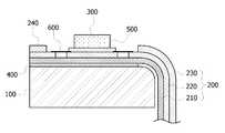
도 2는 본 발명의 일 실시 예에 따른 일체형 금속 회로기판을 도시한 단면도이다.2 is a cross-sectional view showing an integrated metal circuit board according to an embodiment of the present invention.
도 2를 참조하면, 일체형 금속 회로기판은 금속 기판(100) 및 플렉서블 회로기판(200)을 포함하며, 접착층(400)에 의해 금속 기판(100)에 플렉서블 회로기판(200)이 적층결합되어 일체화될 수 있다. 즉, 접착층(400)을 이용하여 금속 기판(100)을 플렉서블 회로기판(200)의 일부 영역에 접착함으로써, 플렉서블 회로기판(200)이 일체화된 금속 회로기판을 제공할 수 있다.Referring to FIG. 2, the integrated metal circuit board includes a
금속 기판(100)은 구리 또는 알루미늄 등의 금속 소재로 형성될 수 있으며, 발광 다이오드 모듈(300)에 의해 발생하는 열을 외부로 방출하는 기능을 수행할 수 있다.The
금속 기판(100)의 상부면에는 접착층(bonding sheet)(400)이 배치될 수 있다. 본 명세서에서는 설명의 용이함을 위하여 도면에 도시된 각 구성요소의 위치를 상부 또는 하부로 표현하나, 이는 그 위치를 한정하는 절대적인 의미가 아니며, 각 구성요소 간의 상대적 위치를 의미하는 것에 불과하다.An
접착층(400)은 접착 필름 등으로 이루어질 수 있으며, 금속 기판(100)의 상부면에 플렉서블 회로기판(200)의 일부 영역을 적층결합하는 기능을 수행할 수 있다.The
금속 기판(100)은 발광 다이오드 모듈(300)의 방열이 용이하도록 플렉서블 회로기판(200)에서 발광 다이오드 모듈(300)이 실장되는 영역에 대응하여 적층결합될 수 있다.The
플렉서블 회로기판(200)은 플렉서블 절연층(210), 도전패턴(220), 보호층(230) 등을 포함할 수 있으며, 플렉서블 회로기판(200)의 상부면에는 발광 다이오드 모듈(300)이 실장될 수 있다.The
플렉서블 절연층(210)으로는 방열 특성이 15W/mK이상인 고방열 절연층이 사용될 수 있다.As the flexible insulating
플렉서블 절연층(210)은 필름, 시트 형태 등의 폴리이미드(polyimide: PI)로 이루어질 수 있으며, 폴리이미드는 카본(carbon: C) 수 1 내지 10 사이의 지방족, 카본 수 1 내지 10 사이의 방향족, 또는 카본 수 1 내지 10 사이의 할로겐 치환 지방족이나 할로겐 치환 방향족을 작용기로 가질 수 있다.The flexible
또한, 플렉서블 절연층(210)은 20㎛ 내지 200㎛의 두께로 형성될 수 있다. 플렉서블 절연층(210)의 두께가 이보다 얇은 경우에는 외부 충격에 쉽게 찢어질 수 있으며, 이보다 두꺼운 경우에는 플렉서블 회로기판(200)의 굴곡력이 낮아지고, 굴곡 시현 시 금속 기판(100)과의 결합면 사이에서 들뜸 현상이 발생할 수 있다.In addition, the flexible insulating
플렉서블 절연층(210)의 하부면 일부와 금속 기판(100)의 상부면에 배치된 접착층(400)을 통해 플렉서블 절연층(210)과 금속 기판(100)이 적층결합될 수 있다. 그리고 플렉서블 절연층(210)의 상부면 및 하부면 중 적어도 일면에는 도전패턴(220)이 형성될 수 있다. 따라서, 도 2에서는 도전패턴(220)이 플렉서블 절연층(210)의 상부면에 형성되는 것으로 도시되어 있으나, 필요에 따라 플렉서블 절연층(210)의 하부면에 형성될 수도 있다.The flexible
도전패턴(220)은 구리 또는 구리를 주성분으로 하는 금속층을 이용하여 형성될 수 있다.The
보호층(230)은 플렉서블 회로기판(200)에 대한 전기적 절연 및 전기적/물리적 충격 완화 기능을 수행할 수 있다. 보호층(230)은 플렉서블 회로기판(200)의 노출면 중 적어도 일부 영역에 형성될 수 있으며, 솔더 레지스트(solder resist) 등을 이용하여 형성될 수 있다.The
발광 다이오드 모듈(300)은 칩 형태로 구현될 수 있으며, 전도성 접착제(500)에 의해 세라믹 기판 없이, 금속 기판(100)과의 결합 영역에 대응되는 플렉서블 회로기판(200)의 도전패턴(220) 상에 직접 실장될 수 있다. 또한, 발광 다이오드 모듈(300)의 애노드(anode) 및 캐소드(cathode) 단자에 연결되는 각 와이어(600)는 도전패턴(220)에 전기적으로 연결될 수 있다.The light emitting
전도성 접착제(500)는 전기 전도성을 가진 접착제로서, AuSn 페이스트 등이 전도성 접착제(500)로 사용될 수 있다.The
이와 같이 본 발명의 실시 예에 따르면, 금속 기판(100) 상에 플렉서블 절연층(210)이 적층결합되고, 플렉서블 절연층(210) 상에 발광 다이오드 모듈(300)이 결합된다. 플렉서블 절연층(210)은 금속 기판(100)과 발광 다이오드 모듈(300) 간의 절연 기능을 수행할 수 있다. 이에 따라, 절연 기능을 수행하는 세라믹 기판을 생략하고, 발광 다이오드 모듈(300)을 금속 기판(100)의 상부에 실장하는 것이 가능하다.As described above, according to an embodiment of the present invention, the flexible insulating
도 3은 본 발명의 다른 실시 예에 따른 일체형 금속 회로기판을 도시한 단면도이다.3 is a cross-sectional view showing an integrated metal circuit board according to another embodiment of the present invention.
도 3의 일체형 금속 회로기판은 도 2에 도시된 본 발명의 일 실시 예에 따른 일체형 금속 회로기판과 금속 기판(100)의 형상을 제외한 전체 구성이 동일하므로 각 구성에 대한 상세한 설명은 생략하기로 한다.The integral metal circuit board of FIG. 3 has the same overall configuration except the shape of the integral metal circuit board and the
도 3을 참조하면, 금속 기판(100)은 플렉서블 회로기판(200)과 적층결합되는 결합면(101)의 외곽부(E)가 곡면 처리될 수 있다. 상세히 하면, 금속 기판(100)의 결합면(101)과, 이 결합면(101)과 연결되는 측면(102)이 완만한 곡면을 이루도록 라운드 처리될 수 있다.Referring to FIG. 3, in the
이러한 금속 기판(100)의 곡면 처리를 통해 도 4에 도시된 바와 같이 플렉서블 회로기판(200)의 절곡 구현 시, 플렉서블 회로기판(200)이 완만한 곡면 각도를 이루며 절곡되기 때문에 절곡으로 인한 플렉서블 회로기판(200)의 크랙 발생을 최소화할 수 있다.When the bending of the
이에 따라 플렉서블 회로기판(200)의 내구성이 더욱 향상될 수 있으며, 결과적으로 전체적인 일체형 금속 회로기판의 신뢰성이 더욱 향상되는 효과가 있다.
Accordingly, the durability of the
상기에서는 본 발명의 바람직한 실시 예를 참조하여 설명하였지만, 해당 기술 분야의 숙련된 당업자는 하기의 특허 청구의 범위에 기재된 본 발명의 사상 및 영역으로부터 벗어나지 않는 범위 내에서 본 발명을 다양하게 수정 및 변경시킬 수 있음을 이해할 수 있을 것이다.
Although described above with reference to preferred embodiments of the present invention, those skilled in the art variously modify and change the present invention without departing from the spirit and scope of the present invention as set forth in the claims below. You can understand that you can.
10 : 금속 회로기판 11, 100 : 금속 기판
12 : 절연층 13, 22, 220 : 도전패턴
14, 23 : 솔더 레지스트 20, 200 : 플렉서블 회로기판
21, 210 : 플렉서블 절연층 30, 300 : 발광 다이오드 모듈
31 : 세라믹 기판 32 : 발광 다이오드
40 : 솔더 210 : 플렉서블 절연층
230: 보호층 400 : 접착층
500 : 전도성 접착제 600 : 와이어10:
12: insulating
14, 23: solder resist 20, 200: flexible circuit board
21, 210: flexible insulating
31: ceramic substrate 32: light emitting diode
40: solder 210: flexible insulating layer
230: protective layer 400: adhesive layer
500: conductive adhesive 600: wire
Claims (7)
Translated fromKorean상기 플렉서블 절연층의 하부면 일부에 상부면이 결합되는 금속 기판; 및
상기 금속 기판과의 결합 영역에 대응하는 상기 플렉서블 절연층의 상부면에 형성된 도전패턴 상에 전도성 접착제를 통해 직접 실장되는 발광 다이오드 모듈을 포함하고,
상기 금속 기판의 상부면에는 접착층이 배치되고, 상기 플렉서블 절연층의 하부면 일부와 상기 금속 기판의 상부면은 상기 접착층을 통해 결합되고,
상기 보호층은 솔더 레지스트를 이용하여 형성되고,
상기 금속 기판은 상기 플렉서블 절연층과 적층결합되는 결합면과 상기 결합면에 연결되는 측면이 곡면을 이루도록 라운드 처리된 일체형 금속 회로기판.
A flexible circuit board including a flexible insulating layer, a conductive pattern formed on at least one surface of the flexible insulating layer, and a protective layer attached to at least one surface of the flexible insulating layer on which the conductive pattern is formed;
A metal substrate having an upper surface coupled to a portion of a lower surface of the flexible insulating layer; And
It includes a light emitting diode module mounted directly on the conductive pattern formed on the upper surface of the flexible insulating layer corresponding to the bonding region with the metal substrate through a conductive adhesive,
An adhesive layer is disposed on an upper surface of the metal substrate, and a portion of a lower surface of the flexible insulating layer and an upper surface of the metal substrate are joined through the adhesive layer,
The protective layer is formed using a solder resist,
The metal substrate is an integrated metal circuit board which is rounded so that a coupling surface laminated with the flexible insulating layer and a side surface connected to the coupling surface form a curved surface.
상기 전도성 접착제는 AuSn 페이스트인 일체형 금속 회로기판.
According to claim 1,
The conductive adhesive is an AuSn paste integral metal circuit board.
상기 플렉서블 절연층은 폴리이미드, 카본 수 1 내지 10 사이의 지방족 또는 방향족을 작용기로 가지는 폴리이미드, 및 카본 수 1 내지 10 사이의 할로겐 치환 지방족 또는 할로겐 치환 방향족을 작용기로 가지는 폴리이미드 중 적어도 하나로 이루어진 일체형 금속 회로기판.
According to claim 1,
The flexible insulating layer is made of at least one of polyimide, polyimide having an aliphatic or aromatic group having 1 to 10 carbons, and polyimide having a halogen substituted aliphatic or halogen substituted aromatic group having 1 to 10 carbons as a functional group. Integral metal circuit board.
상기 플렉서블 절연층은 20㎛ 내지 200㎛의 두께로 형성되는 일체형 금속 회로기판.
According to claim 1,
The flexible insulating layer is an integrated metal circuit board formed to a thickness of 20㎛ to 200㎛.
Priority Applications (1)
| Application Number | Priority Date | Filing Date | Title |
|---|---|---|---|
| KR1020130041165AKR102123555B1 (en) | 2013-04-15 | 2013-04-15 | Integrated metal printed circuit board |
Applications Claiming Priority (1)
| Application Number | Priority Date | Filing Date | Title |
|---|---|---|---|
| KR1020130041165AKR102123555B1 (en) | 2013-04-15 | 2013-04-15 | Integrated metal printed circuit board |
Publications (2)
| Publication Number | Publication Date |
|---|---|
| KR20140123828A KR20140123828A (en) | 2014-10-23 |
| KR102123555B1true KR102123555B1 (en) | 2020-06-16 |
Family
ID=51994344
Family Applications (1)
| Application Number | Title | Priority Date | Filing Date |
|---|---|---|---|
| KR1020130041165AActiveKR102123555B1 (en) | 2013-04-15 | 2013-04-15 | Integrated metal printed circuit board |
Country Status (1)
| Country | Link |
|---|---|
| KR (1) | KR102123555B1 (en) |
Family Cites Families (2)
| Publication number | Priority date | Publication date | Assignee | Title |
|---|---|---|---|---|
| JPS61226994A (en)* | 1985-03-30 | 1986-10-08 | 日本メクトロン株式会社 | Flexible metal base circuit board |
| KR100671545B1 (en)* | 2005-07-01 | 2007-01-19 | 삼성전자주식회사 | LED array module |
- 2013
- 2013-04-15KRKR1020130041165Apatent/KR102123555B1/enactiveActive
Also Published As
| Publication number | Publication date |
|---|---|
| KR20140123828A (en) | 2014-10-23 |
Similar Documents
| Publication | Publication Date | Title |
|---|---|---|
| US7642563B2 (en) | LED package with metal PCB | |
| CN110431664B (en) | Mounting LED elements on a flat carrier | |
| US20080067526A1 (en) | Flexible circuits having improved reliability and thermal dissipation | |
| AU2008201050B2 (en) | Electronic-component-mounting board | |
| KR101431099B1 (en) | Metal printed circuit board, assembly substrate for light emitting diode, assembly body for light emitting diode using the same | |
| US10985303B2 (en) | Method of making an LED device | |
| US10371357B2 (en) | Electronic component and corresponding mounting method | |
| KR102105566B1 (en) | Integrated metal printed circuit board | |
| KR102123555B1 (en) | Integrated metal printed circuit board | |
| KR102130090B1 (en) | Integrated metal printed circuit board | |
| US9923123B2 (en) | Printed circuit board and light-emitting device including same | |
| KR102087864B1 (en) | luminous element module | |
| KR101523000B1 (en) | 3D lighting device | |
| KR101492522B1 (en) | Semiconductor device package | |
| KR101216936B1 (en) | Light emitting diode | |
| KR101242093B1 (en) | LED device improved radient heat efficiency and fabricating method thereof | |
| KR20160118507A (en) | Bendable printed circuit board | |
| JP2022038722A (en) | Luminous module and lighting equipment | |
| CN102934529A (en) | Flexible printed wiring board | |
| JP2012222108A (en) | Light source unit and lighting device |
Legal Events
| Date | Code | Title | Description |
|---|---|---|---|
| PA0109 | Patent application | Patent event code:PA01091R01D Comment text:Patent Application Patent event date:20130415 | |
| PG1501 | Laying open of application | ||
| A201 | Request for examination | ||
| PA0201 | Request for examination | Patent event code:PA02012R01D Patent event date:20180411 Comment text:Request for Examination of Application Patent event code:PA02011R01I Patent event date:20130415 Comment text:Patent Application | |
| E902 | Notification of reason for refusal | ||
| PE0902 | Notice of grounds for rejection | Comment text:Notification of reason for refusal Patent event date:20190813 Patent event code:PE09021S01D | |
| AMND | Amendment | ||
| E601 | Decision to refuse application | ||
| PE0601 | Decision on rejection of patent | Patent event date:20200212 Comment text:Decision to Refuse Application Patent event code:PE06012S01D Patent event date:20190813 Comment text:Notification of reason for refusal Patent event code:PE06011S01I | |
| X091 | Application refused [patent] | ||
| AMND | Amendment | ||
| PX0901 | Re-examination | Patent event code:PX09011S01I Patent event date:20200212 Comment text:Decision to Refuse Application Patent event code:PX09012R01I Patent event date:20191010 Comment text:Amendment to Specification, etc. | |
| PX0701 | Decision of registration after re-examination | Patent event date:20200401 Comment text:Decision to Grant Registration Patent event code:PX07013S01D Patent event date:20200309 Comment text:Amendment to Specification, etc. Patent event code:PX07012R01I Patent event date:20200212 Comment text:Decision to Refuse Application Patent event code:PX07011S01I Patent event date:20191010 Comment text:Amendment to Specification, etc. Patent event code:PX07012R01I | |
| X701 | Decision to grant (after re-examination) | ||
| GRNT | Written decision to grant | ||
| PR0701 | Registration of establishment | Comment text:Registration of Establishment Patent event date:20200610 Patent event code:PR07011E01D | |
| PR1002 | Payment of registration fee | Payment date:20200611 End annual number:3 Start annual number:1 | |
| PG1601 | Publication of registration | ||
| PR1001 | Payment of annual fee | Payment date:20240516 Start annual number:5 End annual number:5 |