KR102118618B1 - Cantilever probe pin card with function of the noise filter and EMI protection - Google Patents
Cantilever probe pin card with function of the noise filter and EMI protectionDownload PDFInfo
- Publication number
- KR102118618B1 KR102118618B1KR1020200023807AKR20200023807AKR102118618B1KR 102118618 B1KR102118618 B1KR 102118618B1KR 1020200023807 AKR1020200023807 AKR 1020200023807AKR 20200023807 AKR20200023807 AKR 20200023807AKR 102118618 B1KR102118618 B1KR 102118618B1
- Authority
- KR
- South Korea
- Prior art keywords
- needle
- insulating layer
- copper tube
- main insulating
- probe pin
- Prior art date
- Legal status (The legal status is an assumption and is not a legal conclusion. Google has not performed a legal analysis and makes no representation as to the accuracy of the status listed.)
- Active
Links
- 239000000523sampleSubstances0.000titleclaimsabstractdescription47
- 239000010410layerSubstances0.000claimsabstractdescription47
- RYGMFSIKBFXOCR-UHFFFAOYSA-NCopperChemical compound[Cu]RYGMFSIKBFXOCR-UHFFFAOYSA-N0.000claimsabstractdescription40
- 229910052802copperInorganic materials0.000claimsabstractdescription40
- 239000010949copperSubstances0.000claimsabstractdescription40
- 239000011241protective layerSubstances0.000claimsabstractdescription27
- 238000005259measurementMethods0.000claimsabstractdescription23
- 239000000758substrateSubstances0.000claimsabstractdescription23
- 239000000463materialSubstances0.000claimsabstractdescription12
- 230000000903blocking effectEffects0.000claimsabstractdescription11
- 238000005452bendingMethods0.000claimsabstractdescription8
- 239000011810insulating materialSubstances0.000claimsabstractdescription6
- 239000004809TeflonSubstances0.000claimsdescription5
- 229920006362Teflon®Polymers0.000claimsdescription5
- OKTJSMMVPCPJKN-UHFFFAOYSA-NCarbonChemical compound[C]OKTJSMMVPCPJKN-UHFFFAOYSA-N0.000claimsdescription4
- 238000001914filtrationMethods0.000claimsdescription4
- 229910021389grapheneInorganic materials0.000claimsdescription4
- 238000009413insulationMethods0.000abstractdescription9
- 238000005516engineering processMethods0.000abstractdescription4
- 238000000034methodMethods0.000description5
- 239000004065semiconductorSubstances0.000description5
- 230000000694effectsEffects0.000description4
- 238000007689inspectionMethods0.000description4
- 238000004519manufacturing processMethods0.000description3
- 238000012360testing methodMethods0.000description3
- 238000000576coating methodMethods0.000description2
- 239000004593EpoxySubstances0.000description1
- 239000000853adhesiveSubstances0.000description1
- 230000001070adhesive effectEffects0.000description1
- 230000002411adverseEffects0.000description1
- 239000000919ceramicSubstances0.000description1
- 238000006243chemical reactionMethods0.000description1
- 239000011248coating agentSubstances0.000description1
- 230000002950deficientEffects0.000description1
- 238000010586diagramMethods0.000description1
- 238000010292electrical insulationMethods0.000description1
- 230000005611electricityEffects0.000description1
- 238000012986modificationMethods0.000description1
- 230000004048modificationEffects0.000description1
- 238000000465mouldingMethods0.000description1
- 238000012545processingMethods0.000description1
- 230000008054signal transmissionEffects0.000description1
Images


Classifications
- G—PHYSICS
- G01—MEASURING; TESTING
- G01R—MEASURING ELECTRIC VARIABLES; MEASURING MAGNETIC VARIABLES
- G01R1/00—Details of instruments or arrangements of the types included in groups G01R5/00 - G01R13/00 and G01R31/00
- G01R1/02—General constructional details
- G01R1/18—Screening arrangements against electric or magnetic fields, e.g. against earth's field
- G—PHYSICS
- G01—MEASURING; TESTING
- G01R—MEASURING ELECTRIC VARIABLES; MEASURING MAGNETIC VARIABLES
- G01R1/00—Details of instruments or arrangements of the types included in groups G01R5/00 - G01R13/00 and G01R31/00
- G01R1/02—General constructional details
- G01R1/06—Measuring leads; Measuring probes
- G01R1/067—Measuring probes
- G01R1/06711—Probe needles; Cantilever beams; "Bump" contacts; Replaceable probe pins
- G01R1/06716—Elastic
- G01R1/06727—Cantilever beams
- G—PHYSICS
- G01—MEASURING; TESTING
- G01R—MEASURING ELECTRIC VARIABLES; MEASURING MAGNETIC VARIABLES
- G01R1/00—Details of instruments or arrangements of the types included in groups G01R5/00 - G01R13/00 and G01R31/00
- G01R1/02—General constructional details
- G01R1/06—Measuring leads; Measuring probes
- G01R1/067—Measuring probes
- G01R1/06711—Probe needles; Cantilever beams; "Bump" contacts; Replaceable probe pins
- G01R1/06733—Geometry aspects
- G01R1/06744—Microprobes, i.e. having dimensions as IC details
- G—PHYSICS
- G01—MEASURING; TESTING
- G01R—MEASURING ELECTRIC VARIABLES; MEASURING MAGNETIC VARIABLES
- G01R1/00—Details of instruments or arrangements of the types included in groups G01R5/00 - G01R13/00 and G01R31/00
- G01R1/02—General constructional details
- G01R1/06—Measuring leads; Measuring probes
- G01R1/067—Measuring probes
- G01R1/073—Multiple probes
- G01R1/07307—Multiple probes with individual probe elements, e.g. needles, cantilever beams or bump contacts, fixed in relation to each other, e.g. bed of nails fixture or probe card
- G—PHYSICS
- G01—MEASURING; TESTING
- G01R—MEASURING ELECTRIC VARIABLES; MEASURING MAGNETIC VARIABLES
- G01R31/00—Arrangements for testing electric properties; Arrangements for locating electric faults; Arrangements for electrical testing characterised by what is being tested not provided for elsewhere
- G01R31/28—Testing of electronic circuits, e.g. by signal tracer
- G01R31/2851—Testing of integrated circuits [IC]
- G01R31/2886—Features relating to contacting the IC under test, e.g. probe heads; chucks
Landscapes
- Physics & Mathematics (AREA)
- General Physics & Mathematics (AREA)
- Engineering & Computer Science (AREA)
- Geometry (AREA)
- Computer Hardware Design (AREA)
- Microelectronics & Electronic Packaging (AREA)
- General Engineering & Computer Science (AREA)
- Measuring Leads Or Probes (AREA)
- Testing Or Measuring Of Semiconductors Or The Like (AREA)
Abstract
Translated fromKoreanDescription
Translated fromKorean본 발명은 노이즈 차단구조를 갖는 마이크로 캔틸레버 프로브 핀카드에 관한 것으로서, 단순 절연처리된 프로브 핀카드의 니들 구조를 개선하여 절연특성을 향상시키고, Femto Level의 측정환경에서 외부의 노이즈에 해당하는 전자파, 온도, 습도로부터 영향을 최소화하여 측정정밀도를 향상시키고 자 한 기술에 관한 것이다.The present invention relates to a micro cantilever probe pin card having a noise blocking structure, improving the needle structure of a simple insulated probe pin card, improving insulation characteristics, and electromagnetic waves corresponding to external noise in a measurement environment of femto level, It is about technology to improve the measurement precision by minimizing the influence from temperature and humidity.
일반적으로 프로브 핀카드는 반도체의 동작을 검사하기 위하여 반도체 칩과 테스트 장비를 연결하는 장치로서, 프로브 카드에 장착되어 있는 프로브 핀이 웨이퍼를 접촉하면서 전기를 보내고, 그때 돌아오는 신호에 따라 불량 반도체 칩을 선별하게 된다.In general, a probe pin card is a device that connects a semiconductor chip and test equipment to check the operation of a semiconductor, and the probe pin mounted on the probe card sends electricity while contacting the wafer, and a defective semiconductor chip according to the returned signal Will be screened.
상기 프로브 카드는 프로브 핀의 배치 방식에 따라 캔틸레버 방식(cantilever type)과 버티컬 방식(Vertical type) 및 MEMS 방식으로 구분되고 있다. 상기 캔틸레버 방식은 PCB기판에 프로브 핀을 접착제로 고정하는 수작업으로 이루어지며, 다른 방식에 비해 기술적 난이도가 낮은 이점을 갖는다.The probe card is classified into a cantilever type, a vertical type, and a MEMS type according to the arrangement method of the probe pin. The cantilever method is made by manually fixing the probe pin to the PCB substrate with an adhesive, and has the advantage of lower technical difficulty than other methods.
최근 들어 전자제품의 기술이 발전함에 따라 반도체 소자 및 OLED 소자 내에 구비된 트랜지스터 및 측정대상 회로에서는 Femto(1000조분의 1) 단위의 Low level측정이 가능한 계측기가 요구되는 실정이다.In recent years, as the technology of electronic products has been developed, a transistor capable of measuring a low level in the Femto (1/1000 trillion) unit is required in transistors and measurement circuits provided in semiconductor devices and OLED devices.
그리고 계측기뿐만 아니라 측정용 탐침도구도 단일 채널 프로브 핀 기준 Leakage Current 특성이 5fA 수준으로 Probe Pin Instrument를 사용한다. 그러나 멀티채널을 이용한 DC Test에서는 측정 환경의 노이즈를 고려하여 100 Femto Ampere 미만의 Leakage 특성을 갖는 프로브 카드를 요구한다. -20V 내지 +20V 영역에서 Femto 단위의 Low level 환경에서는 주변온도, 습도, 전자파와 같은 노이즈 요소에 매우 민감하게 반응하기 때문에 측정회로 루프 내에서 노이즈 신호와 주변 공기의 차폐는 중요한 요소이다.In addition to measuring instruments, probes for measurement use a probe pin instrument with a Leakage Current characteristic of 5fA based on a single channel probe pin. However, in the DC test using multi-channel, considering the noise of the measurement environment, a probe card with a leak characteristic of less than 100 Femto Ampere is required. In the low level environment of the femto unit in the range of -20V to +20V, since it reacts very sensitively to noise elements such as ambient temperature, humidity, and electromagnetic waves, shielding the noise signal and the surrounding air in the measurement circuit loop is an important factor.
특히, Femto 단위의 Low level 환경에서의 측정은 대부분 실험실의 항온, 항습 환경에서 이루어지기 때문에, 노이즈가 잘 고려된 측정 도구를 사용하면 되지만, 양산 환경에서의 측정은 간헐적인 수많은 전자파에 노출되기 때문에 정밀측정에 어려움이 발생하는 문제점이 있었다.In particular, since the measurement in the low level environment of the femto unit is performed in the constant temperature and humidity environment of the laboratory, you can use a measurement tool that considers noise well, but the measurement in the mass production environment is exposed to numerous intermittent electromagnetic waves. There was a problem that difficulty in precision measurement.
관련 선행기술로서, 등록특허 제10-1467382호(캔틸레버 프로브의 적층형 니들 구조)에는 검사대상물과 전기적으로 연결되는 복수개의 전기적 특성 검사장치용 프로브의 니들 구조에 있어서, 상기 프로브의 몸체는 캔틸레버 타입의 니들 형태로 형성되어 일단부가 외부의 전기적 특성 검사 장비와 전기적으로 연결되고, 프로브의 팁부가 상기 프로브의 몸체 타단부로부터 하방으로 벤딩형성되며, 다수의 프로브가 일렬로 배치되도록 벤딩부의 상기 검사대상물로부터의 높이에 따라 분류된 층을 복수의 층으로 적층시키되, 최하단부인 1층에 배치된 프로브들은, 상기 프로브의 팁부와 상기 검사대상물이 이루는 접촉각이 2층에 배치된 프로브들의 상기 접촉각보다 소정의 크기만큼 작도록 형성되는 기술이 개시되어 있다.As a related prior art, in the needle structure of a probe for a plurality of electrical property inspection devices electrically connected to an object to be inspected in Patent No. 10-1467382 (a stacked needle structure of a cantilever probe), the body of the probe is a cantilever type Formed in the form of a needle, one end is electrically connected to an external electrical property inspection equipment, a tip portion of the probe is bent downward from the other end of the probe body, and a plurality of probes are arranged in a row from the inspection object of the bending portion The layers classified according to the height of the layer are stacked into a plurality of layers, but the probes disposed on the bottommost one layer have a predetermined contact angle between the tip portion of the probe and the inspection object and the contact angles of the probes disposed on the second layer. A technique that is formed to be as small as is disclosed.
상기 선행기술은 1층과 2층의 프로브 니들의 밴딩부끼리 서로 접촉되지 않도록 구성하여, 프로브의 변형을 방지하고 내구성을 향상시키기 위한 기술에 관한 것이다. 따라서, 상기 선행기술은 앞서 설명한 바와 같은 Femto 단위의 Low level 환경에서의 전자파 및 온도, 습도 등의 영향을 최소화하기 위한 기술적 해결구성이 존재하지 않으며, 이와 관련된 내용의 암시가 존재하지 않는 기술에 해당한다.The prior art relates to a technique for preventing deformation of a probe and improving durability by configuring the bending portions of the probe needles of the first and second layers to not contact each other. Therefore, the prior art does not have a technical solution for minimizing the effects of electromagnetic waves, temperature, humidity, etc. in a low level environment of the femto unit as described above, and it corresponds to a technology in which there is no suggestion of related content. do.
상기와 같이 5fa Leakage 특성이 있는 대부분의 단일채널 측정툴은 고가에 해당되며, 멀티채널 적용시 큰 비용이 소요되는 관계로 실제 노이즈가 많이 유발되는 양산환경에서 멀티채널의 적용이 어려웠던바, 본 발명은 이를 해결하기 위해 저가로 구현할 수 있는 캔틸레버 방식의 프로브 핀카드에서 노이즈를 현저히 저감할 수 있는 구조로 개선하여, 외부 노이즈가 불가피한 상황에서도 원하는 신호를 정확하게 측정할 수 있도록 한 마이크로 캔틸레버 프로브 핀카드를 제공함에 목적을 두고 있다.As described above, most single channel measurement tools having a 5fa leakage characteristic are expensive, and it is difficult to apply multi-channel in a mass production environment where actual noise is generated due to a large cost when applying multi-channel. To solve this, the cantilever probe pincard, which can be implemented at low cost, has been improved to a structure that can significantly reduce noise, so that the microcantilever probe pincard can accurately measure the desired signal even when external noise is inevitable. The purpose is to provide.
본 발명은 기판부와, 상기 기판부에 설치되며 일정구간 메인절연층으로 코팅처리된 니들과, 상기 니들과 연결되도록 기판부에 설치되어 니들의 측정신호를 제공받는 동축케이블;을 포함하며, 상기 니들의 메인절연층이 형성된 구간에는 메인절연층을 감싸는 형태로 구리재질의 동관부;를 형성하고, 상기 동관부의 내측에는 동관부의 물리적 구부러짐으로부터 메인절연층을 보호하기 위한 절연소재의 보호층;으로 이루어지는 것을 특징으로 한다.
또한 상기 니들과 메인절연층, 보호층 및 동관부는 분리되지 않고 일체로 제작되며, 동관부가 형성된 니들에서 분기하여 동관부의 노이즈를 필터링하기 위한 필터회로를 병렬로 설치하고 기판부에 접지할 수 있다.The present invention includes a substrate portion, a needle installed on the substrate portion and coated with a main insulating layer for a predetermined period, and a coaxial cable installed on the substrate portion to be connected to the needle and receiving a measurement signal from the needle. In the section where the main insulation layer of the needle is formed, a copper tube of copper material is formed in a form surrounding the main insulation layer, and inside the copper tube part, a protective layer of an insulating material for protecting the main insulation layer from physical bending of the copper tube part; It is characterized by being made.
In addition, the needle, the main insulating layer, the protective layer and the copper tube part are integrally manufactured without being separated, and a filter circuit for filtering noise of the copper tube part by branching from the needle where the copper tube part is formed can be installed in parallel and grounded to the substrate part.
삭제delete
또한 상기 보호층은 테프론 재질로 적용되는 것을 특징으로 한다.In addition, the protective layer is characterized in that applied to the Teflon material.
또한 상기 보호층은 메인절연층의 두께보다 더 두껍게 형성되는 것을 특징으로 한다.In addition, the protective layer is characterized in that it is formed thicker than the thickness of the main insulating layer.
또한 상기 보호층의 일측에는 그래핀 재질의 차폐층을 더 포함하는 것을 특징으로 한다.In addition, one side of the protective layer is characterized in that it further comprises a shielding layer of graphene material.
또한 상기 기판부에는 동관부의 노이즈를 필터링하기 위한 필터회로를 형성하는 것을 특징으로 한다.In addition, a filter circuit for filtering noise of the copper tube portion is formed on the substrate portion.
본 발명은 기존의 프로브 핀카드에서 단순절연처리로 이루어진 니들의 구조에서, 절연구간에 대하여 니들의 외부를 감싸는 동관부를 형성함으로써 전자파 차단 및 외부 공기접촉으로 인한 온도, 습도 변화에 따른 영향을 최소화하여 측정 신뢰도를 향상시킬 수 있는 효과가 있다.The present invention minimizes the effect of temperature and humidity changes due to electromagnetic wave blocking and external air contact by forming a copper tube that surrounds the outside of the needle with respect to the insulation section in the structure of the needle made of simple insulation processing in the existing probe pin card. This has the effect of improving measurement reliability.
또한 본 발명은 동관부 내측에 절연재질의 보호층을 더 구성함으로써, 동관부의 물리적 구부러짐에 의해 니들의 메인절연층을 보호하여 Short와 같은 문제를 방지할 수 있고, 동관부와 함께 2중 차폐구조를 갖기 때문에, 노이즈 차단효과를 극대화할 수 있는 구조적 이점을 갖는다.In addition, the present invention further comprises a protective layer made of an insulating material inside the copper tube part, thereby protecting the main insulating layer of the needle by physical bending of the copper tube part to prevent problems such as short, and double shielding structure with the copper tube part Since it has a, it has a structural advantage that can maximize the noise blocking effect.
도 1은 본 발명의 노이즈 차단구조를 갖는 마이크로 캔틸레버 프로브 핀카드의 주요 구성을 개략적으로 나타낸 도면
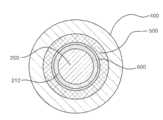
도 2는 본 발명의 니들에 동관부가 형성된 부분을 나타낸 확대 단면도
도 3은 본 발명의 보호층 일측에 차폐층이 더 형성된 또 다른 실시예의 확대 단면도
도 4는 본 발명의 기판부에 필터회로를 더 구성한 실시예를 나타낸 도면
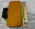
도 5는 본 발명의 프로브 핀카드를 반도체소자,OLED회로소자, RFIC소자, ET parametric 측정 및 테스트를 위해 사용되기 위한 실물을 나타낸 사진
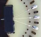
도 6은 도 5의 내부에서 필터 삽입전 필터와 연결되기 위한 GND 부분을 나타낸 사진
도 7은 본 발명의 프로브 핀카드와 종래기술의 프로브 핀카드와 Leakage 특성을 평균과 산포를 통계적으로 비교한 Leakage 전류측정값의 평균과 산포값을 비교한 도표
도 8은 본 발명에 의한 프로브 핀카드와 종래기술의 프로브 핀카드의 니들에 -20V부터 +20V까지 인가전압을 변환하여 측정된 Leakage 전류 특성 값을 비교한 도표1 is a view schematically showing the main configuration of a micro cantilever probe pin card having a noise blocking structure of the present invention
Figure 2 is an enlarged cross-sectional view showing a portion where a copper tube is formed on the needle of the present invention
3 is an enlarged cross-sectional view of another embodiment in which a shielding layer is further formed on one side of the protective layer of the present invention
4 is a view showing an embodiment in which a filter circuit is further configured in the substrate portion of the present invention.
Figure 5 is a photograph showing the real thing to be used for the probe pin card of the present invention for semiconductor devices, OLED circuit devices, RFIC devices, ET parametric measurement and testing
FIG. 6 is a photograph showing a GND portion to be connected to a filter before inserting the filter in the interior of FIG. 5
FIG. 7 is a chart comparing the average and scattered values of the Leakage current measurement values statistically comparing the average and scattered characteristics of the probe pincard of the present invention and the probe pincard of the prior art.
8 is a table comparing the measured leakage current characteristic value by converting the applied voltage from -20V to +20V to the needle of the probe pin card according to the present invention and the probe pin card of the prior art.
이하 본 발명의 바람직한 실시예를 첨부된 도면을 참조하여 상세히 설명하면 다음과 같다. 그리고 본 발명을 설명함에 있어서, 관련된 공지기능 혹은 구성에 대한 구체적인 설명이 본 발명의 요지를 불필요하게 흐릴 수 있다고 판단되는 경우 그 상세한 설명을 생략한다.Hereinafter, preferred embodiments of the present invention will be described in detail with reference to the accompanying drawings. In the following description, when it is determined that the detailed description of the related known functions or configurations may unnecessarily obscure the subject matter of the present invention, the detailed description will be omitted.
본 발명의 노이즈 차단구조를 갖는 마이크로 캔틸레버 프로브 핀카드는 도 1 내지 2에 도시한 바와 같이 기판부(100)와, 상기 기판부(100)에 설치되며 일정구간 메인절연층(210)으로 코팅처리된 니들(200)과, 상기 니들(200)과 연결되도록 기판부(100)에 설치되어 니들(200)의 측정신호를 제공받는 동축케이블(300);을 포함하며, 상기 니들(200)의 메인절연층(210)이 형성된 구간에는 메인절연층(210)을 감싸는 형태로 구리재질의 동관부(400);를 형성하고 상기 동관부(400)의 내측에는 동관부(400)의 물리적 구부러짐으로부터 메인절연층(210)을 보호하기 위한 절연소재의 보호층(500);으로 이루어지는 것을 특징으로 한다.The micro cantilever probe pin card having the noise blocking structure of the present invention is installed on the
상기 기판부(100)는 니들(200)과 동축케이블(300)이 설치되어 신호전송이 이루어지도록 하는 것으로서, 일반적으로 사용되는 PCB기판에 해당되는 구성이다.The
그리고 상기 니들(200)은 기판부(100)에 설치되는 것으로서, 에폭시(또는 세라믹)몰딩에 의해 형성된 고정부재(110)를 통해 니들(200)이 기판부(100)에 고정되도록 하며, 측정부분에 해당하는 니들(200)의 선단부를 제외한 나머지 부분에 해당하는 구간 전체에 메인절연층(210)이 형성되어 있다. 상기 메인절연층(210)은 니들(200)의 기본적인 절연기능을 위해 코팅처리된 구성으로서, 상기 메인절연층(210)만으로 Femto 단위의 Low level 환경에서의 외부 노이즈를 효과적으로 차단할 수 없다.And the
따라서, 상기 니들(200)의 메인절연층(210)이 형성된 구간에는 노이즈를 차단하기 위한 구리재질의 동관부(400)가 메인절연층(210)을 감싸는 형태로 형성된다. 상기 동관부(400)는 외부 전자파의 차폐기능을 담당한다.Thus, in the section where the main
그리고 상기 동관부(400)의 내측에는 동관부(400)의 굴곡부위에 따라 발생되는 물리적 구부러짐으로부터 메인절연층(210)을 보호하기 위한 보호층(500)이 더 형성되어 있다. 상기 보호층(500)은 절연소재로 적용되며, 테프론(Teflon)과 같은 재질로 적용되는 것이 바람직하다. 테프론 재질은 내열성, 내저온성, 전기절연성이 뛰어난 재질로서, 동관부(400)와 함께 외부 노이즈를 차폐하게 된다.In addition, a
만약, 상기 동관부(400) 내측에 보호층(500)을 형성하지 않게 될 경우, 동관부(400)의 구부러진 형상에 따라 메인절연층(210)에 물리적 스트레스를 주어, 니들(200)의 Short 발생이 유발되는 우려가 있다. 따라서, 상기 보호층(500)은 메인절연층(210)의 두께보다 두껍게 형성되는 것이 바람직하다.If, when the
상기와 같이 메인절연층(210)을 포함하는 니들(200)의 외부에 동관부(400)와 보호층(500)을 함께 구성함으로써, 외부공기와의 접촉을 2중으로 차단하기 때문에, 온도와 습도 변화에 따른 악영향을 최소화할 수 있는 것이다.Since the
도 3은 본 발명의 또 다른 실시예를 나타낸 것으로서, 보호층(500)의 일측에 그래핀(Graphene) 재질의 차폐층(600)을 더 포함할 수 있다. 상기 그래핀 재질의 차폐층(600)은 테프론 재질의 보호층(500)에 크게 기대할 수 없던 전자파 차폐기능을 갖도록 한 것으로서, 상기와 같이 차폐층(600)을 더 포함함으로써 2중 절연구조 및 2중 전자파 차폐구조를 갖게 되는 것이다.3 shows another embodiment of the present invention, and may further include a
상기 차폐층(600)은 보호층(500)의 내측에 배치되어 보호층(500)과 메인절연층(210) 사이에 위치할 수 있고, 보호층(500)의 외측에 배치되어 보호층(500)과 동관부(400) 사이에 위치할 수 있다. 상기 차폐층(600)은 코팅방식으로 형성되는 것이 바람직하기 때문에, 제조편의상 도면에 도시한 바와 같이 보호층(500) 내측에 배치되는 것이 좋다.The
아울러, 본 발명의 기판부(100)에는 도 4에 도시한 바와 같이 동관부(400)의 노이즈를 필터링하기 위한 R-C 또는 L-C 필터의 기능을 수행하는 필터회로(700)를 더 구성할 수 있다.In addition, a
도 5 내지 6은 본 발명의 기술내용이 적용된 프로브핀 카드의 실물사진을 나타낸 것으로서, 니들(200)의 신호전달 구간에 동관부(400)가 형성되어 있음을 알 수 있다.5 to 6 shows a real picture of the probe pin card to which the technical contents of the present invention are applied, and it can be seen that the
도 7은 본 발명의 프로브 핀카드와 종래기술의 프로브 핀카드와 Leakage 특성을 평균과 산포를 통계적으로 비교한 Leakage 전류측정값의 평균과 산포값을 비교한 도표를 나타낸 것으로서, 종래기술(도표상 epoxy1, epoxy2)의 Leakage 특성이 좋지않은 반면, 본 발명의 프로브 핀카드는 50fA 수준에 달성하게 되었다.Figure 7 is a probe pin card of the present invention and a probe pin card of the prior art showing a chart comparing the average and scattered values of the Leakage current measurement values statistically comparing the average and the scattering of Leakage properties, While the Leakage properties of epoxy1 and epoxy2) were not good, the probe pincard of the present invention was achieved at a level of 50 fA.
그리고 도 8은 본 발명에 의한 프로브 핀카드와 종래기술의 프로브 핀카드의 니들(200)에 -20V부터 +20V까지 인가전압을 변환하여 측정된 Leakage 전류 특성 값을 비교한 도표를 나타낸 것으로서, 특히 -20V 인가 바이어스 상태에서는 종래기술(도표상 epoxy1, epoxy2)은 노이즈 특성에 따라 오차가 현저하게 상승한 반면, 본 발명의 프로브 핀카드는 -20V에서 +20V 전 영역에 걸쳐 Femto Level의 측정환경에서 안정된 특성을 보이고 있다.And Figure 8 is a probe pin card according to the present invention and the conventional probe pin card of the
이상에서 본 발명은 상기 실시예를 참고하여 설명하였지만 본 발명의 기술사상 범위 내에서 다양한 변형실시가 가능함은 물론이다.In the above, the present invention has been described with reference to the above embodiments, but it is of course possible to perform various modifications within the technical scope of the present invention.
100 : 기판부
110 : 고정부재
200 : 니들
210 : 메인절연층
300 : 동축케이블
400 : 동관부
500 : 보호층
600 : 차폐층
700 : 필터회로
G : GND100: substrate portion
110: fixing member
200: needle
210: main insulation layer
300: coaxial cable
400: Dongguan
500: protective layer
600: shielding layer
700: filter circuit
G: GND
Claims (5)
Translated fromKorean상기 기판부(100)에 설치되며 일정구간 메인절연층(210)으로 코팅처리된 니들(200)과,
상기 니들(200)과 연결되도록 기판부(100)에 설치되어 니들(200)의 측정신호를 제공받는 동축케이블(300);을 포함하며,
상기 니들(200)의 메인절연층(210)이 형성된 구간에는 메인절연층(210)을 감싸는 형태로 구리재질의 동관부(400);를 형성하고,
상기 동관부(400)의 내측에는 동관부(400)의 물리적 구부러짐으로부터 메인절연층(210)을 보호하기 위한 절연소재의 보호층(500);으로 이루어지며
상기 니들(200)과 메인절연층(210), 보호층(500) 및 동관부(400)는 분리되지 않고 일체로 제작되며,
상기 동관부(400)가 형성된 니들(200)에서 분기하여 동관부(400)의 노이즈를 필터링하기 위한 필터회로(700)를 병렬로 설치하고 기판부(100)에 접지한 것을 특징으로 하는 노이즈 차단구조를 갖는 마이크로 캔틸레버 프로브 핀카드.
The substrate portion 100,
Needle 200 is installed on the substrate portion 100 and coated with a main insulating layer 210 for a certain period,
Includes; is installed on the substrate portion 100 to be connected to the needle 200 to receive the measurement signal of the needle 200, a coaxial cable 300;
In the section where the main insulating layer 210 of the needle 200 is formed, a copper tube 400 made of a copper material in a form surrounding the main insulating layer 210 is formed,
The inside of the copper tube part 400 is made of a protective layer 500 of an insulating material for protecting the main insulating layer 210 from the physical bending of the copper tube part 400;
The needle 200 and the main insulating layer 210, the protective layer 500 and the copper tube 400 are not separated and are integrally manufactured,
Noise blocking, characterized in that a filter circuit 700 for filtering noise of the copper tube 400 is installed in parallel and grounded on the substrate 100 by branching from the needle 200 where the copper tube 400 is formed. Micro cantilever probe pincard with structure.
상기 보호층(500)은 테프론 재질로 적용되는 것을 특징으로 하는 노이즈 차단구조를 갖는 마이크로 캔틸레버 프로브 핀카드.
According to claim 1,
The protective layer 500 is a micro cantilever probe pin card having a noise blocking structure, characterized in that applied to a Teflon material.
상기 보호층(500)은 메인절연층(210)의 두께보다 더 두껍게 형성되는 것을 특징으로 하는 노이즈 차단구조를 갖는 마이크로 캔틸레버 프로브 핀카드.
According to claim 1,
The protective layer 500 is a micro cantilever probe pin card having a noise blocking structure characterized in that it is formed thicker than the thickness of the main insulating layer 210.
상기 보호층(500)의 일측에는 그래핀 재질의 차폐층(600)을 더 포함하는 것을 특징으로 하는 노이즈 차단구조를 갖는 마이크로 캔틸레버 프로브 핀카드.
According to claim 1,
A micro cantilever probe pin card having a noise blocking structure, further comprising a shielding layer 600 made of graphene on one side of the protective layer 500.
Priority Applications (1)
| Application Number | Priority Date | Filing Date | Title |
|---|---|---|---|
| KR1020200023807AKR102118618B1 (en) | 2020-02-26 | 2020-02-26 | Cantilever probe pin card with function of the noise filter and EMI protection |
Applications Claiming Priority (1)
| Application Number | Priority Date | Filing Date | Title |
|---|---|---|---|
| KR1020200023807AKR102118618B1 (en) | 2020-02-26 | 2020-02-26 | Cantilever probe pin card with function of the noise filter and EMI protection |
Publications (1)
| Publication Number | Publication Date |
|---|---|
| KR102118618B1true KR102118618B1 (en) | 2020-06-04 |
Family
ID=71081090
Family Applications (1)
| Application Number | Title | Priority Date | Filing Date |
|---|---|---|---|
| KR1020200023807AActiveKR102118618B1 (en) | 2020-02-26 | 2020-02-26 | Cantilever probe pin card with function of the noise filter and EMI protection |
Country Status (1)
| Country | Link |
|---|---|
| KR (1) | KR102118618B1 (en) |
Citations (14)
| Publication number | Priority date | Publication date | Assignee | Title |
|---|---|---|---|---|
| JPH04188080A (en)* | 1990-11-21 | 1992-07-06 | Mitsubishi Electric Corp | coaxial probe needle |
| KR950006472A (en)* | 1993-08-04 | 1995-03-21 | 이노우에 아끼라 | Probe card, coaxial probe beam for probe card and manufacturing method thereof |
| JPH09329638A (en)* | 1996-06-07 | 1997-12-22 | Tokyo Electron Ltd | Inspection pin and inspection device |
| KR19980043156A (en)* | 1995-12-01 | 1998-09-05 | 에릭 더블유. 스트리드 | Low Current Test Card |
| JP2004170181A (en)* | 2002-11-19 | 2004-06-17 | Yokowo Co Ltd | Checking tool for high-frequency/high-speed device |
| JP2005527823A (en)* | 2002-05-23 | 2005-09-15 | カスケード マイクロテック インコーポレイテッド | Probe for testing devices |
| KR100811740B1 (en)* | 2007-06-29 | 2008-03-11 | (주)피티앤케이 | Probe Needle Tube and Manufacturing Method Thereof |
| JP2009294064A (en)* | 2008-06-05 | 2009-12-17 | Totoku Electric Co Ltd | High frequency measuring probe |
| JP2016538540A (en)* | 2013-11-07 | 2016-12-08 | フィルター・センシング・テクノロジーズ・インコーポレイテッドFilter Sensing Technologies,Inc. | Advanced radio frequency sensing probe |
| KR101785636B1 (en)* | 2016-07-18 | 2017-10-17 | 주식회사 에스디에이 | Coaxial probe needle device |
| JP2018048838A (en)* | 2016-09-20 | 2018-03-29 | 横河電機株式会社 | Probe device |
| KR20180042672A (en)* | 2016-10-18 | 2018-04-26 | 삼성전기주식회사 | Probe installaition system, probe unit and test apparatus for electirical characteristics |
| JP2018066567A (en)* | 2016-10-17 | 2018-04-26 | 横河電機株式会社 | Probe device |
| KR102072634B1 (en)* | 2018-10-17 | 2020-02-03 | 한국생산기술연구원 | Probe card needle with improved corrosion and electrical properties |
- 2020
- 2020-02-26KRKR1020200023807Apatent/KR102118618B1/enactiveActive
Patent Citations (14)
| Publication number | Priority date | Publication date | Assignee | Title |
|---|---|---|---|---|
| JPH04188080A (en)* | 1990-11-21 | 1992-07-06 | Mitsubishi Electric Corp | coaxial probe needle |
| KR950006472A (en)* | 1993-08-04 | 1995-03-21 | 이노우에 아끼라 | Probe card, coaxial probe beam for probe card and manufacturing method thereof |
| KR19980043156A (en)* | 1995-12-01 | 1998-09-05 | 에릭 더블유. 스트리드 | Low Current Test Card |
| JPH09329638A (en)* | 1996-06-07 | 1997-12-22 | Tokyo Electron Ltd | Inspection pin and inspection device |
| JP2005527823A (en)* | 2002-05-23 | 2005-09-15 | カスケード マイクロテック インコーポレイテッド | Probe for testing devices |
| JP2004170181A (en)* | 2002-11-19 | 2004-06-17 | Yokowo Co Ltd | Checking tool for high-frequency/high-speed device |
| KR100811740B1 (en)* | 2007-06-29 | 2008-03-11 | (주)피티앤케이 | Probe Needle Tube and Manufacturing Method Thereof |
| JP2009294064A (en)* | 2008-06-05 | 2009-12-17 | Totoku Electric Co Ltd | High frequency measuring probe |
| JP2016538540A (en)* | 2013-11-07 | 2016-12-08 | フィルター・センシング・テクノロジーズ・インコーポレイテッドFilter Sensing Technologies,Inc. | Advanced radio frequency sensing probe |
| KR101785636B1 (en)* | 2016-07-18 | 2017-10-17 | 주식회사 에스디에이 | Coaxial probe needle device |
| JP2018048838A (en)* | 2016-09-20 | 2018-03-29 | 横河電機株式会社 | Probe device |
| JP2018066567A (en)* | 2016-10-17 | 2018-04-26 | 横河電機株式会社 | Probe device |
| KR20180042672A (en)* | 2016-10-18 | 2018-04-26 | 삼성전기주식회사 | Probe installaition system, probe unit and test apparatus for electirical characteristics |
| KR102072634B1 (en)* | 2018-10-17 | 2020-02-03 | 한국생산기술연구원 | Probe card needle with improved corrosion and electrical properties |
Similar Documents
| Publication | Publication Date | Title |
|---|---|---|
| US20140266280A1 (en) | Probe card, probe structure and method for manufacturing the same | |
| JP4535828B2 (en) | Inspection unit manufacturing method | |
| Fang et al. | Noncontact RF voltage sensing of a printed trace via a capacitive-coupled probe | |
| US7403019B2 (en) | Apparatus and method of water absorption test for generator stator winding insulator using cross capacitance | |
| CN100480714C (en) | Shielded probe apparatus for probing semiconductor water | |
| TWI403724B (en) | Inspection contact structure | |
| JP2006337361A (en) | Signal probe and probe assembly | |
| US7782070B2 (en) | Probing device | |
| US20140327462A1 (en) | Test socket providing mechanical stabilization for pogo pin connections | |
| Carlton et al. | Accurate measurement of high-speed package and interconnect parasitics | |
| EP0980004B1 (en) | Microscopic capacitance measurement system and probing system | |
| KR102118618B1 (en) | Cantilever probe pin card with function of the noise filter and EMI protection | |
| JP6109060B2 (en) | Printed circuit board inspection equipment | |
| CN106526322B (en) | Can trace to the source in piece high value resistor measuring system and its source tracing method | |
| Ranieri et al. | A novel 24-GHz bandwidth coaxial probe | |
| Weber et al. | Correlation limits between capacitively coupled transmission line pulsing (CC-TLP) and CDM for a large chip-on-flex assembly | |
| TWI382194B (en) | Soft circuit board test fixture device | |
| US6894513B2 (en) | Multipoint plane measurement probe and methods of characterization and manufacturing using same | |
| Fellner et al. | Transmission line based CDM ESD current target to overcome bandwidth limitations | |
| TWI580980B (en) | Method of measuring electrical length in semiconductor testing apparatus and method of conductive region of wafer alignment | |
| EP2930523B1 (en) | Contactless conductive interconnect testing | |
| JP2013224912A (en) | Connection device and high frequency module | |
| JP2008205282A (en) | Probe card | |
| US11549968B2 (en) | Probing system | |
| TWI569017B (en) | Coaxial probe holding mechanism and electrical characteristics check device |
Legal Events
| Date | Code | Title | Description |
|---|---|---|---|
| PA0109 | Patent application | Patent event code:PA01091R01D Comment text:Patent Application Patent event date:20200226 | |
| PA0201 | Request for examination | ||
| PA0302 | Request for accelerated examination | Patent event date:20200228 Patent event code:PA03022R01D Comment text:Request for Accelerated Examination Patent event date:20200226 Patent event code:PA03021R01I Comment text:Patent Application | |
| PE0902 | Notice of grounds for rejection | Comment text:Notification of reason for refusal Patent event date:20200324 Patent event code:PE09021S01D | |
| E701 | Decision to grant or registration of patent right | ||
| PE0701 | Decision of registration | Patent event code:PE07011S01D Comment text:Decision to Grant Registration Patent event date:20200525 | |
| GRNT | Written decision to grant | ||
| PR0701 | Registration of establishment | Comment text:Registration of Establishment Patent event date:20200528 Patent event code:PR07011E01D | |
| PR1002 | Payment of registration fee | Payment date:20200529 End annual number:3 Start annual number:1 | |
| PG1601 | Publication of registration | ||
| PR1001 | Payment of annual fee | Payment date:20230411 Start annual number:4 End annual number:4 | |
| PR1001 | Payment of annual fee | Payment date:20240416 Start annual number:5 End annual number:5 |