KR102117958B1 - Antifuse conrol circuit and antifuse read starting method thereof - Google Patents
Antifuse conrol circuit and antifuse read starting method thereofDownload PDFInfo
- Publication number
- KR102117958B1 KR102117958B1KR1020140017884AKR20140017884AKR102117958B1KR 102117958 B1KR102117958 B1KR 102117958B1KR 1020140017884 AKR1020140017884 AKR 1020140017884AKR 20140017884 AKR20140017884 AKR 20140017884AKR 102117958 B1KR102117958 B1KR 102117958B1
- Authority
- KR
- South Korea
- Prior art keywords
- read
- voltage
- read voltage
- power
- antifuse
- Prior art date
- Legal status (The legal status is an assumption and is not a legal conclusion. Google has not performed a legal analysis and makes no representation as to the accuracy of the status listed.)
- Active
Links
Images


Classifications
- G—PHYSICS
- G11—INFORMATION STORAGE
- G11C—STATIC STORES
- G11C17/00—Read-only memories programmable only once; Semi-permanent stores, e.g. manually-replaceable information cards
- G11C17/14—Read-only memories programmable only once; Semi-permanent stores, e.g. manually-replaceable information cards in which contents are determined by selectively establishing, breaking or modifying connecting links by permanently altering the state of coupling elements, e.g. PROM
- G11C17/18—Auxiliary circuits, e.g. for writing into memory
- G—PHYSICS
- G11—INFORMATION STORAGE
- G11C—STATIC STORES
- G11C17/00—Read-only memories programmable only once; Semi-permanent stores, e.g. manually-replaceable information cards
- G11C17/14—Read-only memories programmable only once; Semi-permanent stores, e.g. manually-replaceable information cards in which contents are determined by selectively establishing, breaking or modifying connecting links by permanently altering the state of coupling elements, e.g. PROM
- G11C17/16—Read-only memories programmable only once; Semi-permanent stores, e.g. manually-replaceable information cards in which contents are determined by selectively establishing, breaking or modifying connecting links by permanently altering the state of coupling elements, e.g. PROM using electrically-fusible links
- G—PHYSICS
- G11—INFORMATION STORAGE
- G11C—STATIC STORES
- G11C7/00—Arrangements for writing information into, or reading information out from, a digital store
- G11C7/06—Sense amplifiers; Associated circuits, e.g. timing or triggering circuits
- G11C7/08—Control thereof
- G—PHYSICS
- G11—INFORMATION STORAGE
- G11C—STATIC STORES
- G11C7/00—Arrangements for writing information into, or reading information out from, a digital store
- G11C7/20—Memory cell initialisation circuits, e.g. when powering up or down, memory clear, latent image memory
Landscapes
- Read Only Memory (AREA)
- Engineering & Computer Science (AREA)
- Microelectronics & Electronic Packaging (AREA)
- Computer Hardware Design (AREA)
Abstract
Translated fromKoreanDescription
Translated fromKorean본 발명은 안티퓨즈 제어 회로 및 그것에 의한 안티퓨즈 읽기 시작 방법에 관한 것이다. 보다 상세히는, 본 발명은 반도체 메모리 장치의 파워-업시 안티퓨즈에 저장된 데이터의 읽기 시작 타이밍을 제어하는 안티퓨즈 제어 회로 및 그것에 의한 안티퓨즈 읽기 시작 방법에 관한 것이다.The present invention relates to an antifuse control circuit and an antifuse read start method by the same. More specifically, the present invention relates to an antifuse control circuit for controlling the start timing of reading data stored in the antifuse during power-up of a semiconductor memory device and a method for starting antifuse reading by the same.
반도체 메모리 장치(semiconductor memory device)는 실리콘(Si, silicon), 게르마늄(Ge, Germanium), 비화 갈륨(GaAs, gallium arsenide), 인화인듐(InP, indium phospide) 등과 같은 반도체를 이용하여 구현되는 기억장치이다. 반도체 메모리 장치는 크게 휘발성 반도체 메모리 장치(Volatile memory device)와 불휘발성 반도체 메모리 장치(Nonvolatile memory device)로 구분된다.A semiconductor memory device is a storage device implemented using semiconductors such as silicon (Si, silicon), germanium (Ge, Germanium), gallium arsenide (GaAs), indium phospide (InP), and the like. to be. 2. Description of the Related Art Semiconductor memory devices are largely classified into volatile semiconductor memory devices and nonvolatile memory devices.
휘발성 반도체 메모리 장치는 전원 공급이 차단되면 저장하고 있던 데이터가 소멸되는 반도체 메모리 장치이다. 휘발성 반도체 메모리 장치에는 SRAM (Static RAM), DRAM (Dynamic RAM), SDRAM (Synchronous DRAM) 등이 있다.The volatile semiconductor memory device is a semiconductor memory device in which stored data is lost when power supply is cut off. Volatile semiconductor memory devices include static RAM (SRAM), dynamic RAM (DRAM), and synchronous DRAM (SDRAM).
반도체 메모리 장치를 포함하는 시스템에서, 파워-업시 수행되는 읽기 동작을 이하 '파워-업 읽기 동작 (power-up to read operation)'이라 칭한다. 파워-업 읽기 동작시 읽기 페일(Read Fail)를 감소시키기 위해서는, 읽기를 위한 동작 전압이 충분히 증가된 후 읽기 동작이 수행되어야 한다. 예를 들어, 워드 라인 전압이 원하는 전압보다 낮은 상태에서 읽기 동작이 수행되면, 워드 라인 전압을 공급받는 메모리 셀을 통해 상대적으로 적은 셀 전류가 흐르게 되어 읽기 페일이 발생될 수 있다.In a system including a semiconductor memory device, a read operation performed at power-up is hereinafter referred to as a'power-up to read operation'. In order to reduce a read fail during a power-up read operation, a read operation must be performed after the operation voltage for reading is sufficiently increased. For example, when the read operation is performed while the word line voltage is lower than the desired voltage, a relatively small cell current flows through the memory cell receiving the word line voltage, and a read fail may occur.
본 발명의 목적은 안정된 동작 전압에서 안티퓨즈에 대한 읽기 동작을 수행할 수 있도록 안티 퓨즈 읽기 시작 타이밍을 제어하는 안티퓨즈 제어 회로 및 그것에 의한 안티퓨즈 읽기 시작 방법을 제공하는 것이다.An object of the present invention is to provide an anti-fuse control circuit for controlling an anti-fuse read start timing so that a read operation for an anti-fuse can be performed at a stable operating voltage and an anti-fuse read start method by the anti-fuse control circuit.
본 발명에 의한 반도체 메모리 장치의 파워-업시 안티퓨즈 읽기 동작을 제어하는 안티퓨즈 제어 회로는 안티퓨즈에 저장된 데이터를 독출하기 위한 읽기 전압을 생성하는 고전압 생성기 및 상기 안티퓨즈에 대한 읽기 동작 시작 타이밍을 제어하는 읽기 인에이블 신호를 생성하는 센싱 제어기를 포함하고, 상기 센싱 제어기는 소정 시점에서 감지된 상기 읽기 전압의 크기에 응답하여 설정된 지연 시간을 기초로 상기 읽기 인에이블 신호를 활성화한다.An antifuse control circuit that controls an antifuse read operation during power-up of a semiconductor memory device according to the present invention includes a high voltage generator for generating a read voltage for reading data stored in the antifuse and a start timing for the read operation for the antifuse. And a sensing controller generating a controlled read enable signal, wherein the sensing controller activates the read enable signal based on a set delay time in response to the magnitude of the read voltage sensed at a predetermined time.
실시 예에 있어서, 상기 소정 시점은 상기 읽기 전압이 기준 읽기 전압에 도달한 시점을 기초로 결정된다.In an embodiment, the predetermined time point is determined based on a time point at which the read voltage has reached a reference read voltage.
실시 예에 있어서, 상기 지연 시간은 상기 소정 시점에서 상기 읽기 전압의 크기가 작을수록 길게 설정된다.In an embodiment, the delay time is set to be longer as the magnitude of the read voltage is smaller at the predetermined time point.
실시 예에 있어서, 상기 고전압 생성기는 상기 읽기 전압이 상기 기준 읽기 전압에 도달하였는지 여부에 응답하여 비교 신호를 활성화하는 비교부를 포함하고, 상기 센싱 제어기는 외부 전압이 기준 전원 전압에 도달하였는지 여부에 응답하여 파워-업 감지 신호를 활성화하는 파워-업 감지부, 상기 파워-업 감지 신호 및 상기 비교 신호를 기초로 선행 신호를 활성화하는 센싱 제어부 및 상기 선행 신호 및 상기 읽기 전압을 기초로 상기 지연 시간을 설정하는 지연부를 포함한다.In an embodiment, the high voltage generator includes a comparator that activates a comparison signal in response to whether the read voltage has reached the reference read voltage, and the sensing controller responds to whether an external voltage has reached the reference power supply voltage. The power-up detection unit for activating a power-up detection signal, a sensing control unit for activating a preceding signal based on the power-up detection signal and the comparison signal, and the delay time based on the preceding signal and the read voltage. It includes a delay unit to set.
실시 예에 있어서, 상기 고전압 생성기는 상기 비교 신호 및 상기 파워-업 감지 신호에 응답하여 펄스 신호를 생성하는 오실레이터 및 상기 펄스 신호에 응답하여 상기 읽기 전압을 증가하는 펌프부를 더 포함한다.In an embodiment, the high voltage generator further includes an oscillator generating a pulse signal in response to the comparison signal and the power-up detection signal, and a pump unit increasing the read voltage in response to the pulse signal.
실시 예에 있어서, 상기 비교부는 상기 읽기 전압이 상기 기준 읽기 전압에 도달하면 상기 비교 신호를 활성화하고, 상기 센싱 제어기는 상기 외부 전압이 상기 기준 전원 전압에 도달하면 상기 파워-업 감지 신호를 활성화하며, 상기 오실레이터는 상기 비교 신호가 비활성화되고 상기 파워-업 감지 신호가 활성화되었을 때 상기 펄스 신호를 생성한다.In an embodiment, the comparison unit activates the comparison signal when the read voltage reaches the reference read voltage, and the sensing controller activates the power-up detection signal when the external voltage reaches the reference power supply voltage. , The oscillator generates the pulse signal when the comparison signal is deactivated and the power-up detection signal is activated.
실시 예에 있어서, 상기 비교부는 상기 읽기 전압을 분배하여 분배 전압을 생성하는 저항부 및 상기 분배 전압과 기준 전압을 비교하여 상기 비교 신호를 활성화하는 비교기를 포함한다.In an embodiment, the comparator includes a resistor unit that divides the read voltage to generate a divider voltage and a comparator that compares the divider voltage with a reference voltage to activate the compare signal.
실시 예에 있어서, 상기 지연부는 상기 선행 신호에 응답하여 펄스 신호를 생성하는 슈미트 트리거 오실레이터 및 상기 펄스 신호에 응답하여 상기 지연 시간을 설정하고, 설정된 상기 지연 시간을 기초로 상기 읽기 인에이블 신호를 활성화하는 지연 회로를 포함하고, 상기 펄스 신호의 주파수는 상기 읽기 전압의 레벨에 응답하여 가변된다.In an embodiment, the delay unit sets the delay time in response to the Schmitt trigger oscillator generating the pulse signal in response to the preceding signal and the pulse signal, and activates the read enable signal based on the set delay time. And a delay circuit, the frequency of the pulse signal is variable in response to the level of the read voltage.
실시 예에 있어서, 상기 펄스 신호의 주파수는 상기 읽기 전압의 레벨이 작을수록 작은 값으로 설정된다.In an embodiment, the frequency of the pulse signal is set to a smaller value as the level of the read voltage is smaller.
본 발명에 의한 반도체 메모리 장치의 파워-업시 안티퓨즈 읽기 시작 방법은 파워-업 상태 도달 여부를 감지하는 단계, 상기 감지 결과에 응답하여, 안티퓨즈에 저장된 데이터를 독출하기 위한 읽기 전압을 생성하는 단계, 상기 읽기 전압이 기준 읽기 전압에 도달되면, 소정 시점에서 감지된 상기 읽기 전압의 크기에 응답하여 지연 시간을 설정하는 단계 및 상기 설정된 지연 시간 뒤 상기 안티퓨즈에 대한 읽기 동작을 시작하기 위한 읽기 인에이블 신호를 활성화하는 단계를 포함한다.In the semiconductor memory device according to the present invention, an anti-fuse read start method during power-up comprises: detecting whether a power-up state has been reached; generating a read voltage for reading data stored in the anti-fuse in response to the detection result; , When the read voltage reaches a reference read voltage, setting a delay time in response to the magnitude of the read voltage sensed at a predetermined point in time and reading in to start a read operation for the antifuse after the set delay time And activating the enable signal.
실시 예에 있어서, 상기 지연 시간은 상기 소정 시점에서 상기 읽기 전압의 크기가 작을수록 길게 설정된다.In an embodiment, the delay time is set to be longer as the magnitude of the read voltage is smaller at the predetermined time point.
실시 예에 있어서, 상기 소정 시점은 상기 읽기 전압이 기준 읽기 전압에 도달한 시점을 기초로 결정된다.In an embodiment, the predetermined time point is determined based on a time point at which the read voltage has reached a reference read voltage.
실시 예에 있어서, 상기 소정 시점은 상기 읽기 전압이 상기 기준 읽기 전압에 도달한 시점으로부터 미리 지정된 시간 마진이 경과된 시점이다.In an embodiment, the predetermined point in time is a point in time when a predetermined time margin has elapsed from the point when the read voltage reaches the reference read voltage.
실시 예에 있어서, 상기 파워-업 상태 도달 여부를 감지하는 단계는 외부 전압이 기준 전원 전압에 도달하였는지 여부에 응답하여 파워-업 감지 신호를 활성화하는 단계이고, 상기 감지 결과에 응답하여, 상기 안티퓨즈에 저장된 데이터를 독출하기 위한 읽기 전압을 생성하는 단계는 상기 파워-업 감지 신호가 활성화되면 전하를 펌핑하여 상기 읽기 전압을 생성하는 단계이다.In an embodiment, the step of detecting whether the power-up state is reached is a step of activating a power-up detection signal in response to whether an external voltage has reached a reference power voltage, and in response to the detection result, the anti The step of generating a read voltage for reading data stored in a fuse is a step of pumping charge when the power-up detection signal is activated to generate the read voltage.
본 발명에 의한 안티퓨즈 제어 회로 및 그것에 의한 안티퓨즈 읽기 시작 방법은 안정된 동작 전압에서 안티퓨즈에 대한 읽기 동작을 수행할 수 있도록 안티 퓨즈 읽기 시작 타이밍을 제어할 수 있다.The anti-fuse control circuit according to the present invention and the anti-fuse read start method according to the present invention can control the anti-fuse read start timing to perform a read operation for the anti-fuse at a stable operating voltage.
도 1은 본 발명의 실시예에 의한 안티퓨즈 제어 회로를 도시하는 블록도이다.
도 2는 도 1의 안티퓨즈 제어 회로의 실시예를 도시하는 블록도이다.
도 3은 도 2의 안티퓨즈 제어 회로의 동작을 설명하기 위한 타이밍도이다.
도 4는 도 2의 비교부의 실시예를 나타내는 블록도이다.
도 5는 도 2의 지연부의 실시예를 도시하는 블록도이다.
도 6은 도 1의 안티퓨즈 제어 회로를 안티퓨즈 장치에 적용한 실시예이다.
도 7은 본 발명의 실시예에 의한 안티퓨즈 읽기 시작 방법을 도시하는 순서도이다.
도 8은 도 1의 안티퓨즈 제어 회로를 포함하는 메모리 시스템의 블록도이다.
도 9는 모바일 기기에 적용된 본 발명의 응용 예를 도시한 블록도이다.1 is a block diagram showing an antifuse control circuit according to an embodiment of the present invention.
FIG. 2 is a block diagram showing an embodiment of the antifuse control circuit of FIG. 1.
3 is a timing diagram for explaining the operation of the antifuse control circuit of FIG. 2.
FIG. 4 is a block diagram showing an embodiment of the comparison unit of FIG. 2.
5 is a block diagram showing an embodiment of the delay unit of FIG. 2.
6 is an embodiment in which the antifuse control circuit of FIG. 1 is applied to an antifuse device.
7 is a flowchart illustrating a method for starting anti-fuse reading according to an embodiment of the present invention.
8 is a block diagram of a memory system including the antifuse control circuit of FIG. 1.
9 is a block diagram showing an application example of the present invention applied to a mobile device.
이하, 본 발명이 속하는 기술 분야에서 통상의 지식을 가진 자가 본 발명의 기술적 사상을 용이하게 실시할 수 있도록 본 발명의 실시예가 첨부된 도면을 참조하여 설명한다. 또한 이하에서 사용되는 용어들은 오직 본 발명을 설명하기 위하여 사용된 것이며 본 발명의 범위를 한정하기 위해 사용된 것은 아니다. 앞의 일반적인 설명 및 다음의 상세한 설명은 모두 예시적인 것으로 이해되어야 하며, 청구된 발명의 부가적인 설명이 제공되는 것으로 여겨져야 한다.Hereinafter, embodiments of the present invention will be described with reference to the accompanying drawings so that those skilled in the art to which the present invention pertains can easily implement the technical spirit of the present invention. In addition, the terms used below are only used to describe the present invention and are not used to limit the scope of the present invention. It should be understood that both the foregoing general description and the following detailed description are exemplary, and that additional description of the claimed invention is provided.
도 1은 본 발명의 실시예에 의한 안티퓨즈 제어 회로(1)를 도시하는 블록도이다. 안티퓨즈 제어 회로(1)는 반도체 메모리 장치에 포함된 안티퓨즈에 대한 읽기 동작을 제어한다. 도 1을 참조하면, 안티퓨즈 제어 회로(1)는 고전압 발생기(10) 및 센싱 제어기(20)를 포함한다.1 is a block diagram showing an
도 1의 안티퓨즈 제어 회로(1)는 안티퓨즈 읽기 동작을 시작하기 위한 읽기 인에이블 신호(READ_EN)를 활성화할 수 있다. 안티퓨즈 제어 회로(1)는 읽기 전압(Vpp)이 소정의 전압에 도달하였는지 여부를 판별한 뒤, 읽기 전압(Vpp)의 레벨에 응답하여 설정된 지연 시간 후에 읽기 인에이블 신호(READ_EN)를 활성화할 수 있다. 안티퓨즈 제어 회로(1)는 지연 시간을 이용하여, 읽기 전압(Vpp)이 소정의 전압에 도달한 뒤 안정된 전압 레벨에 도달할 때까지의 시간 마진을 확보할 수 있다. 이하 도면을 참조하여 보다 상세히 설명한다.The
고전압 생성 회로(10)는 읽기 전압(Vpp)을 생성한다. 읽기 전압(Vpp)은 안티퓨즈를 읽기 위한 동작 전압으로 사용된다. 예를 들어, 읽기 전압(Vpp)은 안티 퓨즈에 연결된 워드 라인 전압으로 사용될 수 있다.The high
센싱 제어기(20)는 읽기 인에이블 신호(READ_EN)를 활성화한다. 읽기 인에이블 신호(READ_EN)는 안티퓨즈 읽기 동작의 시작 타이밍을 지시하는 신호이다. 센싱 제어기(20)는 읽기 인에이블 신호(READ_EN)의 활성화를 지연하기 위한 지연기(21)를 포함한다.The
안티퓨즈 읽기 동작시 읽기 페일을 감소시키기 위하여, 읽기 전압(Vpp)의 레벨은 읽기 인에이블 신호(READ_EN)가 활성화되기 전 안정화되어야 한다. 또한, 리셋 핀(Reset Pin)이 없는 모바일 디램(Mobile DRAM)에 포함된 안티퓨즈의 경우, 파워-업 상태에 도달된 후 커맨드가 입력되기 전 읽기 동작이 수행되어야 한다. 따라서 읽기 동작 시작에 대한 시간 마진은 일정 길이 이하를 유지하여야 한다. 이하의 도면들에서는 모바일 디램(Mobile DRAM)에 포함된 안티퓨즈를 제어하기 위한 안티퓨즈 제어 회로를 기준으로 설명한다. 그러나 이는 일실시예에 불과하며 본 발명의 안티퓨즈 제어 회로 및 그에 의한 안티퓨즈 읽기 시작 방법은 모바일 디램에 한정되지 않는다.In order to reduce the read fail during the antifuse read operation, the level of the read voltage Vpp must be stabilized before the read enable signal READ_EN is activated. In addition, in the case of an antifuse included in a mobile DRAM without a reset pin, a read operation must be performed before a command is input after reaching a power-up state. Therefore, the time margin for the start of the read operation should be kept below a certain length. In the following drawings, an antifuse control circuit for controlling an antifuse included in a mobile DRAM will be described. However, this is only an example, and the antifuse control circuit of the present invention and the antifuse reading start method therefor are not limited to the mobile DRAM.
센싱 제어기(20)는, 외부 전압(VDD)의 레벨이 소정의 기준 전원 전압 레벨에 도달하면, 고전압 발생기(10)에 파워-업 감지 신호(PVCCH)를 제공한다. 고전압 발생기(10)는 파워 업 감지 신호(PVCCH)에 응답하여 읽기 전압(Vpp)의 레벨을 증가시킨다. 예를 들어, 고전압 발생기(10)는 파워 업 감지 신호(PVCCH)에 응답하여 전하를 펌핑하여 읽기 전압(Vpp)의 레벨을 증가시킬 수 있다.The
읽기 전압(Vpp)의 레벨이 소정의 기준 읽기 전압 레벨에 도달하면, 고전압 발생기(10)는 비교 신호(COMP)를 활성화시킨다. 고전압 발생기(10)는 비교 신호(COMP)를 센싱 제어기(20)에 제공한다.When the level of the read voltage Vpp reaches a predetermined reference read voltage level, the
센싱 제어기(20)는 비교 신호(COMP)가 활성화된 때로부터 소정의 시간 후, 읽기 전압(Vpp)의 레벨을 감지한다. 센싱 제어기(20)의 지연부(21)는 감지된 읽기 전압(Vpp)의 레벨을 기초로 지연 시간을 설정할 수 있다. 지연 시간은 감지된 읽기 전압(Vpp)의 레벨이 낮을수록 길게 설정될 수 있다. 지연부(21)는 설정된 지연 시간이 경과된 후 읽기 인에이블 신호(READ_EN)를 활성화할 수 있다.The
상술된 안티퓨즈 제어 회로(1)는 읽기 전압(Vpp)이 소정의 전압에 도달하였는지 여부를 판별한 뒤, 소정의 지연 시간 후 읽기 인에이블 신호(READ_EN)를 활성화할 수 있다. 지연 시간은 읽기 전압(Vpp)의 레벨에 응답하여 설정된다. 안티퓨즈 제어 회로(1)는 지연 시간을 이용하여, 읽기 전압(Vpp)이 소정의 전압에 도달한 뒤 안정된 전압 레벨에 도달할 때까지의 시간 마진을 확보할 수 있다.The above-described
도 2는 도 1의 안티퓨즈 제어 회로의 실시예를 도시하는 블록도이다. 도 2를 참조하면, 안티퓨즈 제어 회로(100)는 고전압 생성기(110) 및 센싱 제어기(120)를 포함한다.FIG. 2 is a block diagram showing an embodiment of the antifuse control circuit of FIG. 1. Referring to FIG. 2, the
안티퓨즈 제어 회로(100)는 읽기 전압(Vpp)이 소정의 전압에 도달하였는지 여부를 판별한 뒤, 읽기 전압(Vpp)의 레벨에 응답하여 설정된 지연 시간 후 읽기 인에이블 신호(READ_EN)를 활성화할 수 있다. 안티퓨즈 제어 회로(100)는 지연 시간을 이용하여, 읽기 전압(Vpp)이 소정의 전압에 도달한 뒤 안정된 전압 레벨에 도달할 때까지의 시간 마진을 확보할 수 있다.The
고전압 생성기(110)는 비교부(111), 오실레이터(112) 및 펌프부(113)를 포함한다. 고전압 생성기(110)는 피드백 루프를 이용하여, 읽기 전압(Vpp)을 일정한 레벨로 생성 및 유지할 수 있다.The
비교부(111)는 펌프부(113)로부터 읽기 전압(Vpp)을 제공받는다. 비교부(111)는 읽기 전압이 소정의 기준 읽기 전압에 도달하였는지 여부를 판별한다. 비교부(111)는 상기 판별 결과에 응답하여 비교 신호(COMP)를 활성화한다. 예를 들어, 비교부(111)에서 생성되는 비교 신호(COMP)는 읽기 전압(Vpp)이 기준 읽기 전압보다 낮을 때 활성화될 수 있다. 비교부(111)는 비교 신호(COMP)를 오실레이터(112) 및 센싱 제어기(120)에 제공한다.The
오실레이터(112)는 비교부(111)로부터 제공된 비교 신호(COMP) 및 센싱 제어기(120)로부터 제공된 파워-업 감지 신호(PVCCH)에 응답하여 펄스 신호를 생성한다. 예를 들어, 오실레이터(112)는 비교 신호(COMP)가 비활성화 상태이고 파워-업 감지 신호(PVCCH)가 활성화된 상태일 때 펄스 신호를 생성할 수 있다.The
펌프부(113)는 오실레이터(112)로부터 제공된 펄스 신호에 응답하여 전하를 펌핑한다. 펌프부(113)의 펌핑 동작에 응답하여, 펌프부(113)에서 생성되는 읽기 전압(Vpp)의 레벨이 증가된다. 펌프부(113)의 펌핑 동작은 읽기 전압(Vpp)의 레벨이 기준 읽기 전압에 도달될 때까지 지속된다.The
센싱 제어기(120)는 파워-업 감지부(121), 센싱 제어부(122) 및 지연부(123)를 포함한다. 센싱 제어기(120)는 설정된 지연 시간 후 읽기 인에이블 신호(READ_EN)를 활성화할 수 있다.The
파워-업 감지부(121)는 외부 전압(VDD)이 소정의 기준 전원 전압에 도달하면 파워-업 감지 신호(PVCCH)를 활성화할 수 있다. 파워-업 감지부(121)는 파워-업 감지 신호(PVCCH)를 오실레이터(112) 및 센싱 제어부(122)에 제공한다.The power-up
센싱 제어부(122)는 비교부(111)로부터 비교 신호(COMP)를 제공받는다. 또, 센싱 제어부(122)는 파워-업 감지부(121)로부터 파워-업 감지 신호(PVCCH)를 제공받는다. 센싱 제어부(122)는 비교 신호(COMP) 및 파워-업 감지 신호(PVCCH)에 응답하여 선행 신호(PRE)를 활성화할 수 있다. 센싱 제어부(122)는 비교 신호(COMP) 및 파워-업 감지 신호(PNCCH)가 활성화된 때 선행 신호(PRE)를 활성화할 수 있다. 센싱 제어부(122)는 선행 신호(PRE)를 지연부(123)에 제공한다.The
지연부(123)는 선행 신호(PRE)가 활성화되면, 펌프부(113)로부터 제공된 읽기 전압(Vpp)의 레벨을 감지한다. 지연부(123)는 선행 신호(PRE)가 활성화된 뒤 소정의 시간 후 읽기 전압(Vpp)의 레벨을 감지할 수 있다. 예를 들어, 지연부(123)는 파워 업 감지 신호(PVCCH)가 활성화된 시점부터 소정의 시간 마진, 예를 들어 20us, 후 읽기 전압(Vpp)의 레벨을 감지할 수 있다.The
지연부(123)는 감지된 읽기 전압(Vpp)의 레벨을 기초로 지연 시간을 설정할 수 있다. 예를 들어, 지연부(123)는 읽기 전압(Vpp)의 레벨이 낮을수록 긴 지연 시간을 설정할 수 있다. 이때, 지연부(123)는 지연 시간에 의한 안티퓨즈 읽기 동작 완료 시점이 커맨드 입력 시점을 초과하지 않도록 지연 시간을 설정할 수 있다. 지연부(123)는 설정된 지연 시간 후 읽기 인에이블 신호(READ_EN)를 활성화할 수 있다.The
도 3은 도 2의 안티퓨즈 제어 회로(100)의 동작을 설명하기 위한 타이밍도이다. 도 3을 참조하면, 안티퓨즈 제어 회로(100)는 지연 시간(delay)을 이용하여, 읽기 전압(Vpp)이 소정의 전압에 도달한 뒤 안정된 전압 레벨에 도달할 때까지의 시간 마진을 확보할 수 있다.3 is a timing diagram for explaining the operation of the
외부로부터 외부 전압(VDD)이 제공되면, t1에서 외부 전압(VDD)의 레벨이 기준 전원 전압 레벨에 도달된다. 외부 전압(VDD)의 레벨이 기준 전원 전압 레벨에 도달하면, 파워-업 감지부(도 2 참조, 121)에 의하여 파워-업 감지 신호(PVCCH)가 활성화된다.When the external voltage VDD is provided from the outside, the level of the external voltage VDD reaches the reference power supply voltage level at t1. When the level of the external voltage VDD reaches the reference power voltage level, the power-up detection signal PVCCH is activated by the power-up detection unit (see FIG. 2, 121 ).
파워-업 감지 신호(PVCCH)가 활성화됨에 응답하여, 오실레이터(도 2 참조, 112) 및 펌프부(도 2 참조, 113)에 의하여 읽기 전압(Vpp)의 레벨이 증가된다. t2에서, 읽기 전압(Vpp)의 레벨이 소정의 기준 읽기 전압 레벨에 도달된다. 읽기 전압(Vpp)의 레벨이 기준 읽기 전압 레벨에 도달하면, 비교부(도 2 참조, 111)에 의하여 비교 신호(COMP)가 활성화된다.In response to the activation of the power-up detection signal PVCCH, the level of the read voltage Vpp is increased by the oscillator (see FIG. 2, 112) and the pump unit (see FIG. 2, 113). At t2, the level of the read voltage Vpp reaches a predetermined reference read voltage level. When the level of the read voltage Vpp reaches the reference read voltage level, the comparison signal COMP is activated by the comparator (see FIG. 2, 111 ).
파워-업 감지 신호(PVCCH) 및 비교 신호(COMP)에 응답하여, t3에서 선행 신호(PRE)가 활성화된다. 이때 읽기 전압(Vpp)의 레벨에 응답하여, 지연부(도 2 참조, 123)에서 소정의 지연 시간(delay)이 설정된다. 지연부(123)는 읽기 전압(Vpp)의 레벨이 낮을수록 긴 지연 시간을 설정할 수 있다.In response to the power-up detection signal PVCCH and the comparison signal COMP, the preceding signal PRE is activated at t3. At this time, in response to the level of the read voltage Vpp, a predetermined delay time is set in the delay unit (see FIG. 2, 123 ). The
t3으로부터 설정된 지연 시간이 지난 후, t4에서 지연부(123)에 의하여 읽기 인에이블 신호(READ_EN)가 활성화된다.After the set delay time from t3, the read enable signal READ_EN is activated by the
도 2 및 도 3을 참조하면, 안티퓨즈 제어 회로(100)는 비교 신호(COMP)를 이용하여 읽기 전압(Vpp)이 소정의 기준 읽기 전압에 도달되었는지 여부를 판단할 수 있다. 더하여, 안티퓨즈 제어 회로(100)는 지연부(123)를 이용하여 읽기 전압(Vpp)의 크기에 따라 설정되는 지연 시간을 제공함으로써, 비교 신호(COMP) 발생 후 읽기 전압(Vpp)의 크기가 가변되거나 원하는 전압에 미달되는 경우에도 안정된 환경에서 안티퓨즈 읽기 동작이 수행되도록 제어할 수 있다. 2 and 3, the
도 4는 도 2의 비교부의 실시예를 나타내는 블록도이다. 도 4를 참조하면, 비교부(111)는 저항부(111a) 및 비교기(111b)를 포함한다. 저항부(111a)는 제 1 저항(R1), 제 2 저항(R2)를 포함한다.FIG. 4 is a block diagram showing an embodiment of the comparison unit of FIG. 2. Referring to FIG. 4, the
제 1 저항(R1) 및 제 2 저항(R2)은 펌핑부(도 2 참조, 113)로부터 제공된 읽기 전압(Vpp)을 분배하여 분배 전압(Vdiv)을 생성한다. 분배 전압(Vdiv)의 레벨은 제 1 및 제 2 저항(R1, R2)의 저항비에 응답하여 결정될 수 있다.The first resistor R1 and the second resistor R2 divide the read voltage Vpp provided from the pumping unit (refer to FIG. 2, 113) to generate a distribution voltage Vdiv. The level of the distribution voltage Vdiv may be determined in response to the resistance ratios of the first and second resistors R1 and R2.
비교기(111b)는 분배 전압(Vdiv)과 기준 전압(Vref)의 크기를 비교한다. 비교기(111b)는 비교 결과에 응답하여 비교 신호(COMP)를 활성화한다. 예를 들어, 비교기(111b)는 분배 전압(Vdiv)의 레벨이 기준 전압(Vref) 레벨 이상이면 비교 신호(COMP)를 활성화할 수 있다.The
상술된 동작을 참조하면, 비교 신호(COMP)는 분배 전압(Vdiv)이 소정의 기준 전압(Vref)에 도달하면 활성화된다. 분배 전압(Vdiv)은 읽기 전압(Vpp)이 소정의 분배비로 분배된 전압이므로, 비교 신호(COMP)는 읽기 전압(Vpp)이 소정의 기준 읽기 전압에 도달하면 활성화될 수 있다. 즉, 비교부(111)는 분배 전압(Vdiv)을 이용하여, 읽기 전압(Vpp)의 레벨이 원하는 소정의 기준 읽기 전압에 도달하였는지 여부를 감지하는 감지 회로를 구성한다. Referring to the above-described operation, the comparison signal COMP is activated when the distribution voltage Vdiv reaches a predetermined reference voltage Vref. Since the distribution voltage Vdiv is a voltage at which the read voltage Vpp is divided at a predetermined distribution ratio, the comparison signal COMP may be activated when the read voltage Vpp reaches a predetermined reference read voltage. That is, the
도 5는 도 2의 지연부의 실시예를 도시하는 블록도이다. 도 5를 참조하면, 지연부(123)는 슈미트 트리거 오실레이터(123a) 및 지연 회로(123b)를 포함한다.5 is a block diagram showing an embodiment of the delay unit of FIG. 2. Referring to FIG. 5, the
지연부(123)는 센싱 제어부(도 2 참조, 122)로부터 제공된 선행 신호(PRE) 및 펌핑부(도 2 참조, 113)로부터 제공된 읽기 전압(Vpp)에 응답하여 읽기 인에이블 신호(READ_EN)를 활성화할 수 있다.The
슈미트 트리거 오실레이터(123a)는 선행 신호(PRE)가 활성화됨에 응답하여 펄스 신호를 발생한다. 슈미트 트리거 오실레이터(123a)에 포함된 슈미트 트리거의 임계 포인트(Threshold Point)는 읽기 전압(Vpp)에 의하여 제어될 수 있다.The
슈미트 트리거 오실레이터(123a)에서 발생되는 펄스 신호의 주파수 및 듀티비(Duty rate)는 슈미트 트리거의 임계 포인트(Threshold Point)에 응답하여 가변된다. 즉, 슈미트 트리거 오실레이터(123a)에서 발생되는 펄스 신호의 주파수 및 듀티비는 읽기 전압(Vpp)에 의하여 가변될 수 있다. 예를 들어, 펄스 신호의 주파수는 읽기 전압(Vpp)이 작을수록 작은 값을 가질 수 있다. 펄스 신호의 주파수가 작은 값을 가지면, 펄스 신호의 주기는 길어진다. 슈미트 트리거 오실레이터(123a)에서 발생되는 펄스 신호의 주파수에 응답하여 지연 시간이 설정된다.The frequency and duty rate of the pulse signal generated by the
딜레이 회로(123b)는 슈미트 트리거 오실레이터(123a)로부터 입력된 펄스 신호에 응답하여, 설정된 지연 시간 후 읽기 인에이블 신호(READ_EN)를 활성화한다.The
상술된 동작을 참조하면, 지연부(123)는 슈미트 트리거 오실레이터(123a)를 이용하여, 읽기 전압(Vpp)레벨을 기초로 지연 시간을 설정할 수 있다. 지연부(123)는 설정된 지연 시간 후 읽기 인에이블 신호(READ_EN)를 활성화하여 안정된 환경에서 안티퓨즈 읽기 동작이 수행되도록 할 수 있다. Referring to the above-described operation, the
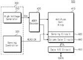
도 6은 도 1의 안티퓨즈 제어 회로를 안티퓨즈 장치에 적용한 실시예이다. 도 6을 참조하면, 안티퓨즈 장치(400)는 안티퓨즈 셀 어레이(410), 어드레스 디코더(420), 센싱 회로(430), 열 게이트 회로(440), 데이터 입출력 회로(450) 및 안티퓨즈 제어 회로(300)를 포함한다.6 is an embodiment in which the antifuse control circuit of FIG. 1 is applied to an antifuse device. Referring to FIG. 6, the antifuse device 400 includes an
어드레스 디코더(420), 센싱 회로(430) 및 열 게이트 회로(440)는 독출 회로(Read Circuit)를 구성할 수 있다. 안티퓨즈 장치(400)는 독출 회로를 이용하여 안티퓨즈 셀 어레이(410)에 저장된 데이터를 독출할 수 있다.The
안티퓨즈 제어 회로(300)는 고전압 발생기(310) 및 센싱 제어기(320)를 포함한다. 도 6의 고전압 발생기(310) 및 센싱 제어기(320)는 도 1의 고전압 발생기(10) 및 센싱 제어기(20)와 동일한 구성 및 동작 원리를 가질 수 있다.The
안티퓨즈 셀 어레이(410)는 복수의 워드 라인들과 복수의 비트 라인들과 연결되는 복수의 안티퓨즈 셀들을 포함한다. 각 안티퓨즈 셀들은 전기적으로 프로그램/소거될 수 있는 노어형 플래시 메모리 셀(NOR-type Flash Memory Cell), 제조시 이온 주입 공정을 통해 프로그램될 수 있는 마스크 롬 셀(Mask ROM Cell), 혹은 전기적으로 프로그램 가능한 강유전체 메모리 셀로 구현될 수 있다. 그러나 이는 예시적인 것으로 본 발명에 있어 안티퓨즈 셀의 종류는 한정되지 않는다.The
센싱 회로(430)는 어드레스 디코더(420)에 의하여 선택된 영역에 배열된 안티퓨즈 셀에 저장된 데이터를 감지한다. 센싱 회로(430)에서 감지된 데이터는 열 게이트 회로(440)를 통해 데이터 입출력 회로(450)로 전달된다.The
한편, 안티퓨즈 제어 회로(300)는 안티퓨즈 셀 어레이에 저장된 데이터를 독출하기 위한 읽기 전압(Vpp)을 생성한다. 또한, 안티퓨즈 제어 회로(300)는 안티퓨즈 셀 어레이에 대한 읽기 동작을 제어하기 위한 읽기 인에이블 신호(READ_EN)를 생성한다.Meanwhile, the
안티퓨즈 제어 회로(300)는 생성된 읽기 전압(Vpp)을 어드레스 디코더(420)에 제공한다. 또, 안티퓨즈 제어 회로(300)는 안티퓨즈 읽기 동작을 제어하기 위한 읽기 인에이블 신호(READ_EN)를 어드레스 디코더(420) 및 센싱 회로(430)에 제공한다.The
도 1을 참조하여 설명된 바와 같이, 안티퓨즈 제어 회로(300)는 읽기 전압(Vpp)이 소정의 전압에 도달하였는지 여부를 판별한 뒤, 소정의 지연 시간 후 읽기 인에이블 신호(READ_EN)를 활성화할 수 있다. 지연 시간은 읽기 전압(Vpp)의 레벨에 응답하여 설정된다. 안티퓨즈 제어 회로(300)를 포함하는 안티퓨즈 장치(400)는 지연 시간을 이용하여, 읽기 전압(Vpp)이 소정의 전압에 도달한 뒤 안정된 전압 레벨에 도달할 때까지의 시간 마진을 확보할 수 있다.As described with reference to FIG. 1, the
도 7은 본 발명의 실시예에 의한 안티퓨즈 읽기 시작 방법을 도시하는 순서도이다.7 is a flowchart illustrating a method for starting anti-fuse reading according to an embodiment of the present invention.
S110 단계에서, 파워-업 상태에 도달했는지 여부가 감지된다. 파워-업 상태는 외부로부터 제공된 외부 전압이 소정의 기준 전원 전압에 도달한 상태를 의미한다. 파워-업 상태는 파워-업 감지부(도 2 참조, 121)에 의하여 감지될 수 있다.In step S110, it is detected whether the power-up state has been reached. The power-up state means a state in which an external voltage provided from the outside has reached a predetermined reference power supply voltage. The power-up state may be detected by the power-up detection unit (see FIG. 2, 121).
S110 단계에서 파워-업 상태에 도달한 경우, S120 단계에서, 전하가 펌핑되고, 펌핑된 전하에 의하여 읽기 전압(Vpp)의 레벨이 증가된다. 읽기 전압(Vpp)은 고전압 발생기(도 2 참조, 110)에 의하여 펌핑될 수 있다.When the power-up state is reached in step S110, the charge is pumped in step S120, and the level of the read voltage Vpp is increased by the pumped charge. The read voltage Vpp may be pumped by a high voltage generator (see FIG. 2, 110).
S130 단계에서, 읽기 전압(Vpp)과 기준 읽기 전압(Vref)의 레벨이 비교된다. 기준 읽기 전압(Vref)은 미리 지정된 소정 레벨의 전압이다. 읽기 전압(Vpp)이 기준 읽기 전압(Vref)에 도달되지 않았으면, S120 단계의 펌핑 동작이 지속된다.In step S130, the level of the read voltage Vpp and the reference read voltage Vref are compared. The reference read voltage Vref is a voltage of a predetermined level specified in advance. If the read voltage Vpp has not reached the reference read voltage Vref, the pumping operation of step S120 is continued.
S130 단계에서 읽기 전압(Vpp)이 기준 읽기 전압(Vref)에 도달되면, S140 단계에서, 소정의 시간 마진 후 읽기 전압(Vpp)의 레벨이 감지된다. 예를 들어 20us의 시간 마진 후 읽기 전압(Vpp)의 레벨이 감지할 수 있다. S140 단계에서 제공되는 시간 마진은 미리 설정될 수 있다.When the read voltage Vpp reaches the reference read voltage Vref in step S130, the level of the read voltage Vpp is sensed after a predetermined time margin in step S140. For example, the level of the read voltage (Vpp) can be detected after a time period of 20us. The time margin provided in step S140 may be set in advance.
감지된 읽기 전압(Vpp)의 레벨에 응답하여 지연 시간이 설정된다. 설정된 지연 시간동안 안티퓨즈 셀 어레이(도 6 참조, 410)에 대한 읽기 인에이블 신호(도 2 참조, READ_EN)의 활성화가 지연된다.The delay time is set in response to the detected level of the read voltage Vpp. During the set delay time, activation of the read enable signal (see FIG. 2, READ_EN) for the antifuse cell array (see FIG. 6, 410) is delayed.
S150 단계에서, 읽기 인에이블 신호(READ_EN)가 활성화된다. 읽기 인에이블 신호에 응답하여 안티퓨즈에 저장된 데이터가 독출될 수 있다.In step S150, the read enable signal READ_EN is activated. Data stored in the antifuse may be read in response to the read enable signal.
본 발명에 의한 안티퓨즈 읽기 시작 방법에 따르면, 읽기 인에이블 신호(READ_EN)는 읽기 전압(Vpp)이 소정의 전압에 도달하였는지 여부가 판별된 뒤, 소정의 지연 시간 후 활성화될 수 있다. 지연 시간은 읽기 전압(Vpp)의 레벨에 응답하여 설정된다. 상술된 안티퓨즈 읽기 시작 방법에 의하면, 지연 시간을 이용하여, 읽기 전압(Vpp)이 소정의 전압에 도달한 뒤 안정된 전압 레벨에 도달할 때까지의 시간 마진이 확보될 수 있다.According to the anti-fuse read start method according to the present invention, the read enable signal READ_EN may be activated after a predetermined delay after determining whether the read voltage Vpp has reached a predetermined voltage. The delay time is set in response to the level of the read voltage Vpp. According to the above-described antifuse read start method, a delay time can be used to ensure a time margin until the read voltage Vpp reaches a predetermined voltage and then reaches a stable voltage level.
도 8은 도 1의 안티퓨즈 제어 회로를 포함하는 메모리 시스템의 블록도이다.8 is a block diagram of a memory system including the antifuse control circuit of FIG. 1.
도 8을 참조하면, 메모리 시스템은 메모리 콘트롤러(2000)와 다이나믹 랜덤 억세스 메모리(1000:DRAM)를 포함할 수 있다. 상기 DRAM(1000)은 시스템 버스(B1)을 통해 상기 메모리 콘트롤러(2000)와 연결되어, 데이터, 어드레스, 및 코맨드를 수신할 수 있다. 또한, 상기 DRAM(1000)은 상기 시스템 버스(B1)을 통해 상기 메모리 콘트롤러(2000)로 메모리 셀로부터 리드된 데이터를 제공할 수 있다.Referring to FIG. 8, the memory system may include a
상기 메모리 콘트롤러(2000)는 정해진 인터페이스를 통해 미도시된 호스트와 연결될 수 있다.The
상기 DRAM(1000)은 도 1과 같은 회로 구성을 가지는 고전압 생성기(1001) 및 센싱 제어기(1002)를 채용할 수 있다. 상기 메모리 시스템 내에서, 상기 DRAM(1000)은 파워-업 동작시 읽기 전압(Vpp)이 소정의 전압에 도달하였는지 여부를 판별한 뒤, 읽기 전압(Vpp)의 레벨에 응답하여 설정된 지연 시간 후 읽기 인에이블 신호(READ_EN)를 활성화할 수 있다. DRAM(1000)은 지연 시간을 이용하여, 읽기 전압(Vpp)이 소정의 전압에 도달한 뒤 안정된 전압 레벨에 도달할 때까지의 시간 마진을 확보할 수 있다. 따라서, 그러한 DRAM(1000)을 포함하는 메모리 시스템의 파워-업 읽기 동작의 안정성이 개선될 수 있다.The
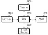
도 9는 모바일 기기에 적용된 본 발명의 응용 예를 도시한 블록도이다.9 is a block diagram showing an application example of the present invention applied to a mobile device.
도 9를 참조하면, 모바일 기기, 예컨대 노트북이나 휴대용 전자기기는 마이크로 프로세싱 유닛(1100,MPU), 디스플레이(1400), 인터페이스 유닛(1300), DRAM(1000), 및 솔리드 스테이트 드라이브(3000)를 포함할 수 있다.Referring to FIG. 9, a mobile device, such as a laptop or portable electronic device, includes a
상기 MPU(1100), DRAM(1000), 및 SSD(3000)는 경우에 따라 하나의 칩으로 제조 또는 패키징될 수 있다. 예를 들어, 상기 DRAM(1000) 및 플래시 메모리(3000)는 상기 모바일 기기에 임베디드될 수도 있다.The
상기 모바일 기기가 휴대용 통신 디바이스인 경우에, 인터페이스 유닛(1300)에는 통신 데이터의 송수신 및 데이터 변복조 기능을 수행하는 모뎀 및 트랜시버가 연결될 수 있다.When the mobile device is a portable communication device, a modem and a transceiver for transmitting and receiving communication data and data demodulation function may be connected to the
상기 MPU(1100)는 미리 설정된 프로그램에 따라 상기 모바일 기기의 제반 동작을 제어한다.The
상기 DRAM(1000)은 상기 MPU(1100)에 연결되며, 상기 MPU(1100)의 버퍼 메모리 또는 메인 메모리로서 기능할 수 있다. 상기 DRAM(1000)은 도 1과 같은 회로 구성을 가지는 고전압 생성기(1001) 및 센싱 제어기(1002)를 채용할 수 있다. 상기 메모리 시스템 내에서, 상기 DRAM(1000)은 파워-업 동작시 읽기 전압(Vpp)이 소정의 전압에 도달하였는지 여부를 판별한 뒤, 읽기 전압(Vpp)의 레벨에 응답하여 설정된 지연 시간 후 읽기 인에이블 신호(READ_EN)를 활성화할 수 있다. DRAM(1000)은 지연 시간을 이용하여, 읽기 전압(Vpp)이 소정의 전압에 도달한 뒤 안정된 전압 레벨에 도달할 때까지의 시간 마진을 확보할 수 있다. 따라서, 그러한 DRAM(1000)을 포함하는 모바일 기기의 파워-업 읽기 동작의 안정성이 개선될 수 있다.The
상기 플래시 메모리(3000)는 노아 타입 혹은 낸드 타입 플래시 메모리일 수 있다.The
상기 디스플레이(1400)는 백라이트를 갖는 액정이나 LED 광원을 갖는 액정 또는 OLED 등의 소자로서 터치 스크린을 가질 수 있다. 상기 디스플레이(1400)은 문자,숫자,그림 등의 이미지를 컬러로 표시하는 출력 소자로서 기능한다.The
상기 모바일 기기는 모바일 통신 장치의 위주로 설명되었으나, 필요한 경우에 구성 요소를 가감하여 스마트 카드로서 기능할 수 있다.Although the mobile device has been mainly described as a mobile communication device, if necessary, it can function as a smart card by adding or subtracting components.
상기 모바일 기기는 별도의 인터페이스를 외부의 통신 장치와 연결될 수 있다. 상기 통신 장치는 DVD(digital versatile disc) 플레이어, 컴퓨터, 셋 탑 박스(set top box, STB), 게임기, 디지털 캠코더 등일 수 있다.The mobile device may be connected to a separate interface with an external communication device. The communication device may be a digital versatile disc (DVD) player, a computer, a set top box (STB), a game machine, or a digital camcorder.
비록 도면에는 도시되지 않았지만, 상기 모바일 기기에는 응용 칩셋(Application chipset), 카메라 이미지 프로세서(Camera Image Processor: CIS), 모바일 디램 등이 더 제공될 수 있음은 이 분야의 통상적인 지식을 가진 자에게 자명하다.Although not shown in the drawing, it is obvious to those skilled in the art that the mobile device may further be provided with an application chipset, a camera image processor (CIS), and a mobile DRAM. Do.
상기 모바일 기기를 형성하는 칩들은 다양한 형태들의 패키지를 이용하여 실장될 수 있다. 예를 들면, 칩들은 PoP(Package on Package), Ball grid arrays(BGAs), Chip scale packages(CSPs), Plastic Leaded Chip Carrier(PLCC), Plastic Dual In-Line Package(PDIP), Die in Waffle Pack, Die in Wafer Form, Chip On Board(COB), Ceramic Dual In-Line Package(CERDIP), Plastic Metric Quad Flat Pack(MQFP), Thin Quad Flatpack(TQFP), Small Outline(SOIC), Shrink Small Outline Package(SSOP), Thin Small Outline(TSOP), Thin Quad Flatpack(TQFP), System In Package(SIP), Multi Chip Package(MCP), Wafer-level Fabricated Package(WFP), Wafer-Level Processed Stack Package(WSP) 등의 패키지로서 단일 패키지화될 수 있다.Chips forming the mobile device may be mounted using various types of packages. For example, the chips are PoP (Package on Package), Ball grid arrays (BGAs), Chip scale packages (CSPs), Plastic Leaded Chip Carrier (PLCC), Plastic Dual In-Line Package (PDIP), Die in Waffle Pack, Die in Wafer Form, Chip On Board (COB), Ceramic Dual In-Line Package (CERDIP), Plastic Metric Quad Flat Pack (MQFP), Thin Quad Flatpack (TQFP), Small Outline (SOIC), Shrink Small Outline Package (SSOP) ), Thin Small Outline (TSOP), Thin Quad Flatpack (TQFP), System In Package (SIP), Multi Chip Package (MCP), Wafer-level Fabricated Package (WFP), Wafer-Level Processed Stack Package (WSP), etc. It can be packaged as a single package.
한편, 도 9에서 플래시 메모리가 채용되는 것을 예로 들었으나, 다양한 종류의 불휘발성 스토리지가 사용될 수 있다.On the other hand, the flash memory is employed as an example in FIG. 9, but various types of nonvolatile storage may be used.
상기 불휘발성 스토리지는 텍스트, 그래픽, 소프트웨어 코드 등과 같은 다양한 데이터 형태들을 갖는 데이터 정보를 저장할 수 있다.The non-volatile storage may store data information having various data types such as text, graphics, and software code.
상기 불휘발성 스토리지는, 예를 들면, EEPROM(Electrically Erasable Programmable Read-Only Memory), 플래시 메모리(flash memory), MRAM(Magnetic RAM), 스핀전달토크 MRAM (Spin-Transfer Torque MRAM), Conductive bridging RAM(CBRAM), FeRAM (Ferroelectric RAM), OUM(Ovonic Unified Memory)라고도 불리는 PRAM(Phase change RAM), 저항성 메모리 (Resistive RAM: RRAM 또는 ReRAM), 나노튜브 RRAM (Nanotube RRAM), 폴리머 RAM(Polymer RAM: PoRAM), 나노 부유 게이트 메모리(Nano Floating Gate Memory: NFGM), 홀로그래픽 메모리 (holographic memory), 분자 전자 메모리 소자(Molecular Electronics Memory Device), 또는 절연 저항 변화 메모리(Insulator Resistance Change Memory)로 구현될 수 있다.The non-volatile storage is, for example, EEPROM (Electrically Erasable Programmable Read-Only Memory), flash memory (flash memory), MRAM (Magnetic RAM), spin-transfer torque MRAM (Spin-Transfer Torque MRAM), Conductive bridging RAM ( CBRAM), FeRAM (Ferroelectric RAM), Phase Change RAM (PRAM), also called OUM (Ovonic Unified Memory), Resistive RAM (Resistive RAM: RRAM or ReRAM), Nanotube RRAM (Nanotube RRAM), Polymer RAM (PoRAM): PoRAM ), Nano Floating Gate Memory (NFGM), Holographic Memory, Molecular Electronics Memory Device, or Insulator Resistance Change Memory .
본 발명의 상세한 설명에서는 구체적인 실시예에 관하여 설명하였으나, 본 발명의 범위에서 벗어나지 않는 한도 내에서 여러 가지로 변형될 수 있다. 예를 들어, 비교부, 오실레이터, 펌프부, 파워-업 감지부, 센싱 제어부 및 지연부의 세부적 구성은 사용 환경이나 용도에 따라 다양하게 변화 또는 변경될 수 있을 것이다. 본 발명에서 사용된 특정한 용어들은 본 발명을 설명하기 위한 목적에서 사용된 것이며 그 의미를 한정하거나 특허 청구범위에 기재된 본 발명의 범위를 제한하기 위하여 사용된 것은 아니다. 그러므로 본 발명의 범위는 상술한 실시예에 국한되어서는 안되며 후술하는 특허 청구범위 뿐만 아니라 이 발명의 특허 청구범위와 균등한 범위에 대하여도 적용되어야 한다.In the detailed description of the present invention, specific embodiments have been described, but may be modified in various ways without departing from the scope of the present invention. For example, detailed configurations of the comparison unit, the oscillator, the pump unit, the power-up detection unit, the sensing control unit, and the delay unit may be variously changed or changed according to the use environment or use. The specific terms used in the present invention are used for the purpose of describing the present invention and are not used to limit the meaning or limit the scope of the present invention described in the claims. Therefore, the scope of the present invention should not be limited to the above-described embodiments, and should be applied not only to the claims described below, but also to the claims and equivalents of the present invention.
1: 안티퓨즈 제어 회로
10: 고전압 생성기
20: 센싱 제어기
21: 지연부1: Antifuse control circuit
10: high voltage generator
20: sensing controller
21: delay
Claims (10)
Translated fromKorean안티퓨즈에 저장된 데이터를 독출하기 위한 읽기 전압을 생성하는 고전압 생성기; 및
상기 안티퓨즈에 대한 읽기 동작 시작 타이밍을 제어하는 읽기 인에이블 신호를 생성하는 센싱 제어기를 포함하고,
상기 센싱 제어기는 소정 시점에서 감지된 상기 읽기 전압의 크기에 응답하여 설정된 지연 시간을 기초로 상기 읽기 인에이블 신호를 활성화하되,
상기 지연 시간은 상기 소정 시점에서 상기 읽기 전압의 크기가 작을수록 길게 설정되는 안티퓨즈 제어 회로.In an antifuse control circuit controlling an antifuse read operation at power-up of a semiconductor memory device:
A high voltage generator that generates a read voltage for reading data stored in the antifuse; And
And a sensing controller generating a read enable signal for controlling the start timing of the read operation for the antifuse,
The sensing controller activates the read enable signal based on a delay time set in response to the magnitude of the read voltage sensed at a predetermined point in time.
The delay time is set at the predetermined time, the smaller the magnitude of the read voltage, the longer the antifuse control circuit is set.
상기 소정 시점은 상기 읽기 전압이 기준 읽기 전압에 도달한 시점을 기초로 결정되는 안티퓨즈 제어 회로.According to claim 1,
The predetermined time point is determined based on the time point at which the read voltage reaches a reference read voltage.
상기 고전압 생성기는 상기 읽기 전압이 기준 읽기 전압에 도달하였는지 여부에 응답하여 비교 신호를 활성화하는 비교부를 포함하고,
상기 센싱 제어기는 외부 전압이 기준 전원 전압에 도달하였는지 여부에 응답하여 파워-업 감지 신호를 활성화하는 파워-업 감지부;
상기 파워-업 감지 신호 및 상기 비교 신호를 기초로 선행 신호를 활성화하는 센싱 제어부; 및
상기 선행 신호 및 상기 읽기 전압을 기초로 상기 지연 시간을 설정하는 지연부를 포함하는 안티퓨즈 제어 회로.According to claim 1,
The high voltage generator includes a comparator that activates a comparison signal in response to whether the read voltage has reached a reference read voltage,
The sensing controller includes a power-up detection unit that activates a power-up detection signal in response to whether an external voltage has reached a reference power voltage;
A sensing control unit activating a preceding signal based on the power-up detection signal and the comparison signal; And
And a delay unit configured to set the delay time based on the preceding signal and the read voltage.
상기 고전압 생성기는 상기 비교 신호 및 상기 파워-업 감지 신호에 응답하여 펄스 신호를 생성하는 오실레이터; 및
상기 펄스 신호에 응답하여 상기 읽기 전압을 증가하는 펌프부를 더 포함하는 안티퓨즈 제어 회로.The method of claim 4,
The high voltage generator is an oscillator that generates a pulse signal in response to the comparison signal and the power-up detection signal; And
And a pump unit that increases the read voltage in response to the pulse signal.
상기 비교부는 상기 읽기 전압이 상기 기준 읽기 전압에 도달하면 상기 비교 신호를 활성화하고, 상기 센싱 제어기는 상기 외부 전압이 상기 기준 전원 전압에 도달하면 상기 파워-업 감지 신호를 활성화하며, 상기 오실레이터는 상기 비교 신호가 비활성화되고 상기 파워-업 감지 신호가 활성화되었을 때 상기 펄스 신호를 생성하는 안티퓨즈 제어 회로.The method of claim 5,
The comparator activates the comparison signal when the read voltage reaches the reference read voltage, the sensing controller activates the power-up detection signal when the external voltage reaches the reference power voltage, and the oscillator An antifuse control circuit that generates the pulse signal when a comparison signal is deactivated and the power-up detection signal is activated.
상기 비교부는 상기 읽기 전압을 분배하여 분배 전압을 생성하는 저항부; 및
상기 분배 전압과 기준 전압을 비교하여 상기 비교 신호를 활성화하는 비교기를 포함하는 안티퓨즈 제어 회로.The method of claim 4,
The comparison unit divides the read voltage to generate a distribution voltage resistor; And
And a comparator that compares the divided voltage and a reference voltage to activate the comparison signal.
파워-업 상태 도달 여부를 감지하는 단계;
상기 감지 결과에 응답하여, 안티퓨즈에 저장된 데이터를 독출하기 위한 읽기 전압을 생성하는 단계;
상기 읽기 전압이 기준 읽기 전압에 도달되면, 소정 시점에서 감지된 상기 읽기 전압의 크기에 응답하여 지연 시간을 설정하는 단계; 및
상기 설정된 지연 시간 뒤 상기 안티퓨즈에 대한 읽기 동작을 시작하기 위한 읽기 인에이블 신호를 활성화하는 단계를 포함하되,
상기 지연 시간은 상기 소정 시점에서 상기 읽기 전압의 크기가 작을수록 길게 설정되는 안티퓨즈 읽기 시작 방법.In the method of starting an anti-fuse read during power-up of a semiconductor memory device:
Detecting whether a power-up state has been reached;
Generating a read voltage for reading data stored in the antifuse in response to the detection result;
When the read voltage reaches a reference read voltage, setting a delay time in response to the magnitude of the read voltage sensed at a predetermined point in time; And
After activating the read enable signal for starting the read operation for the anti-fuse after the set delay time,
The delay time is set to be longer as the magnitude of the read voltage is smaller at the predetermined time point.
상기 파워-업 상태 도달 여부를 감지하는 단계는 외부 전압이 기준 전원 전압에 도달하였는지 여부에 응답하여 파워-업 감지 신호를 활성화하는 단계이고,
상기 감지 결과에 응답하여, 상기 안티퓨즈에 저장된 데이터를 독출하기 위한 읽기 전압을 생성하는 단계는 상기 파워-업 감지 신호가 활성화되면 전하를 펌핑하여 상기 읽기 전압을 생성하는 단계인 안티퓨즈 읽기 시작 방법.The method of claim 8,
The step of detecting whether the power-up state has been reached is a step of activating the power-up detection signal in response to whether the external voltage has reached the reference power voltage,
In response to the detection result, generating a read voltage for reading data stored in the anti-fuse is a step of generating a read voltage by pumping charge when the power-up detection signal is activated. .
Priority Applications (2)
| Application Number | Priority Date | Filing Date | Title |
|---|---|---|---|
| KR1020140017884AKR102117958B1 (en) | 2014-02-17 | 2014-02-17 | Antifuse conrol circuit and antifuse read starting method thereof |
| US14/512,024US9373411B2 (en) | 2014-02-17 | 2014-10-10 | Antifuse control circuit and antifuse reading method |
Applications Claiming Priority (1)
| Application Number | Priority Date | Filing Date | Title |
|---|---|---|---|
| KR1020140017884AKR102117958B1 (en) | 2014-02-17 | 2014-02-17 | Antifuse conrol circuit and antifuse read starting method thereof |
Publications (2)
| Publication Number | Publication Date |
|---|---|
| KR20150096951A KR20150096951A (en) | 2015-08-26 |
| KR102117958B1true KR102117958B1 (en) | 2020-06-02 |
Family
ID=54059035
Family Applications (1)
| Application Number | Title | Priority Date | Filing Date |
|---|---|---|---|
| KR1020140017884AActiveKR102117958B1 (en) | 2014-02-17 | 2014-02-17 | Antifuse conrol circuit and antifuse read starting method thereof |
Country Status (2)
| Country | Link |
|---|---|
| US (1) | US9373411B2 (en) |
| KR (1) | KR102117958B1 (en) |
Families Citing this family (4)
| Publication number | Priority date | Publication date | Assignee | Title |
|---|---|---|---|---|
| TWI578325B (en)* | 2015-08-18 | 2017-04-11 | 力旺電子股份有限公司 | Antifuse-type one time programming memory cell and array structure with same |
| KR102513328B1 (en) | 2016-12-08 | 2023-03-24 | 에스케이하이닉스 주식회사 | Semiconductor device, semiconductor system and operating method for the same |
| KR102738510B1 (en)* | 2018-10-18 | 2024-12-06 | 주식회사 엘엑스세미콘 | Automotive lamp control device |
| US11817163B2 (en)* | 2020-07-16 | 2023-11-14 | Changxin Memory Technologies, Inc. | Circuit for detecting state of anti-fuse storage unit and memory device thereof |
Family Cites Families (13)
| Publication number | Priority date | Publication date | Assignee | Title |
|---|---|---|---|---|
| US6178501B1 (en)* | 1998-04-28 | 2001-01-23 | Micron Technology. Inc. | Method and apparatus for initializing a memory device |
| US5978297A (en)* | 1998-04-28 | 1999-11-02 | Micron Technology, Inc. | Method and apparatus for strobing antifuse circuits in a memory device |
| KR100687848B1 (en) | 1999-01-09 | 2007-02-27 | 주식회사 하이닉스반도체 | Repair circuit with antifuse program / lead device |
| KR100376265B1 (en) | 1999-12-29 | 2003-03-17 | 주식회사 하이닉스반도체 | Memory repair circuit using an antifuse having a MOS structure |
| KR100616215B1 (en)* | 1999-12-29 | 2006-08-25 | 주식회사 하이닉스반도체 | Repair circuit using antifuse |
| US6630724B1 (en)* | 2000-08-31 | 2003-10-07 | Micron Technology, Inc. | Gate dielectric antifuse circuits and methods for operating same |
| KR100420125B1 (en) | 2002-02-02 | 2004-03-02 | 삼성전자주식회사 | Non-volatile semiconductor memory device and power-up to read method thereof |
| KR100470168B1 (en)* | 2002-05-27 | 2005-02-07 | 주식회사 하이닉스반도체 | Antifuse Circuit |
| US8159894B2 (en)* | 2007-08-28 | 2012-04-17 | Broadcom Corporation | One time programmable memory |
| KR20100063294A (en) | 2008-12-03 | 2010-06-11 | 삼성전자주식회사 | Anti-fuse circuit having a protection circuit |
| JP2010165428A (en) | 2009-01-16 | 2010-07-29 | Toshiba Corp | Nonvolatile semiconductor memory device and control method thereof |
| JP5270598B2 (en) | 2010-03-10 | 2013-08-21 | スパンション エルエルシー | Nonvolatile memory device |
| KR20130098039A (en)* | 2012-02-27 | 2013-09-04 | 삼성전자주식회사 | Semiconductor device capable of rescuing defective characteristics after packaging |
- 2014
- 2014-02-17KRKR1020140017884Apatent/KR102117958B1/enactiveActive
- 2014-10-10USUS14/512,024patent/US9373411B2/enactiveActive
Also Published As
| Publication number | Publication date |
|---|---|
| US9373411B2 (en) | 2016-06-21 |
| US20150235712A1 (en) | 2015-08-20 |
| KR20150096951A (en) | 2015-08-26 |
Similar Documents
| Publication | Publication Date | Title |
|---|---|---|
| US9767883B2 (en) | Semiconductor memory device that performs a refresh operation | |
| KR102187485B1 (en) | Nonvolatile memory device and sensing method thereof | |
| KR102475458B1 (en) | Power on reset circuit and semiconductor memory device having the same | |
| US9190120B2 (en) | Storage device including reset circuit and method of resetting thereof | |
| KR102084547B1 (en) | Nonvolatile memory device, memory system having the same, external power controlling method thereof | |
| CN106340318B (en) | Power-on reset circuit and semiconductor memory device including the same | |
| CN105654988B (en) | Memory system and method of operation | |
| US20140169101A1 (en) | Method compensation operating voltage, flash memory device, and data storage device | |
| KR101652333B1 (en) | Variable resistance memory device and program method thereof | |
| KR102117958B1 (en) | Antifuse conrol circuit and antifuse read starting method thereof | |
| US9330781B2 (en) | Nonvolatile memory device and memory system including the same | |
| KR20150141239A (en) | Auxiliary power supply device and nonvolatile memory system including the same | |
| US20160180928A1 (en) | Electronic device and operating method for the same | |
| CN103886899A (en) | Nonvolatile memory apparatus | |
| KR101785006B1 (en) | Memory system including nonvolatile memory and method of controlling thereof | |
| KR20130021706A (en) | Circuit for generating write signal, variable resistance memory device, and method for operating the device | |
| KR20180058442A (en) | Power on reset circuit and semiconductor memory device having the same | |
| US9865344B2 (en) | Electronic device and method for operating electronic device | |
| US20150009742A1 (en) | Semiconductor memory device having improved fuse sensing reliability in slow power-up operation and method for reading fuse block thereby | |
| KR20120080884A (en) | Nonvolatile memory device using variable resistive element and memory system comprising the same | |
| KR102107072B1 (en) | System including memory controller which manages power of memory | |
| KR102324267B1 (en) | Semiconductor device and semiconductor system | |
| KR102088835B1 (en) | Array e-fuse boot-up scheme and semiconductor device using the same | |
| US10263511B2 (en) | Charge pump switching controller for reducing standby current and charge pumping apparatus using the same | |
| US9842648B1 (en) | Memory apparatus and reference voltage setting method thereof |
Legal Events
| Date | Code | Title | Description |
|---|---|---|---|
| PA0109 | Patent application | Patent event code:PA01091R01D Comment text:Patent Application Patent event date:20140217 | |
| PG1501 | Laying open of application | ||
| PA0201 | Request for examination | Patent event code:PA02012R01D Patent event date:20190104 Comment text:Request for Examination of Application Patent event code:PA02011R01I Patent event date:20140217 Comment text:Patent Application | |
| E902 | Notification of reason for refusal | ||
| PE0902 | Notice of grounds for rejection | Comment text:Notification of reason for refusal Patent event date:20191217 Patent event code:PE09021S01D | |
| E701 | Decision to grant or registration of patent right | ||
| PE0701 | Decision of registration | Patent event code:PE07011S01D Comment text:Decision to Grant Registration Patent event date:20200510 | |
| GRNT | Written decision to grant | ||
| PR0701 | Registration of establishment | Comment text:Registration of Establishment Patent event date:20200527 Patent event code:PR07011E01D | |
| PR1002 | Payment of registration fee | Payment date:20200528 End annual number:3 Start annual number:1 | |
| PG1601 | Publication of registration | ||
| PR1001 | Payment of annual fee | Payment date:20230426 Start annual number:4 End annual number:4 |