KR102114000B1 - Differential silicon oxide etch - Google Patents
Differential silicon oxide etchDownload PDFInfo
- Publication number
- KR102114000B1 KR102114000B1KR1020157009495AKR20157009495AKR102114000B1KR 102114000 B1KR102114000 B1KR 102114000B1KR 1020157009495 AKR1020157009495 AKR 1020157009495AKR 20157009495 AKR20157009495 AKR 20157009495AKR 102114000 B1KR102114000 B1KR 102114000B1
- Authority
- KR
- South Korea
- Prior art keywords
- substrate processing
- region
- etching
- plasma
- substrate
- Prior art date
- Legal status (The legal status is an assumption and is not a legal conclusion. Google has not performed a legal analysis and makes no representation as to the accuracy of the status listed.)
- Active
Links
Images

Classifications
- H—ELECTRICITY
- H01—ELECTRIC ELEMENTS
- H01L—SEMICONDUCTOR DEVICES NOT COVERED BY CLASS H10
- H01L21/00—Processes or apparatus adapted for the manufacture or treatment of semiconductor or solid state devices or of parts thereof
- H01L21/02—Manufacture or treatment of semiconductor devices or of parts thereof
- H01L21/04—Manufacture or treatment of semiconductor devices or of parts thereof the devices having potential barriers, e.g. a PN junction, depletion layer or carrier concentration layer
- H01L21/18—Manufacture or treatment of semiconductor devices or of parts thereof the devices having potential barriers, e.g. a PN junction, depletion layer or carrier concentration layer the devices having semiconductor bodies comprising elements of Group IV of the Periodic Table or AIIIBV compounds with or without impurities, e.g. doping materials
- H01L21/30—Treatment of semiconductor bodies using processes or apparatus not provided for in groups H01L21/20 - H01L21/26
- H01L21/302—Treatment of semiconductor bodies using processes or apparatus not provided for in groups H01L21/20 - H01L21/26 to change their surface-physical characteristics or shape, e.g. etching, polishing, cutting
- H01L21/306—Chemical or electrical treatment, e.g. electrolytic etching
- H01L21/3065—Plasma etching; Reactive-ion etching
- H—ELECTRICITY
- H01—ELECTRIC ELEMENTS
- H01J—ELECTRIC DISCHARGE TUBES OR DISCHARGE LAMPS
- H01J37/00—Discharge tubes with provision for introducing objects or material to be exposed to the discharge, e.g. for the purpose of examination or processing thereof
- H01J37/32—Gas-filled discharge tubes
- H01J37/32009—Arrangements for generation of plasma specially adapted for examination or treatment of objects, e.g. plasma sources
- H01J37/32082—Radio frequency generated discharge
- H01J37/32091—Radio frequency generated discharge the radio frequency energy being capacitively coupled to the plasma
- H—ELECTRICITY
- H01—ELECTRIC ELEMENTS
- H01J—ELECTRIC DISCHARGE TUBES OR DISCHARGE LAMPS
- H01J37/00—Discharge tubes with provision for introducing objects or material to be exposed to the discharge, e.g. for the purpose of examination or processing thereof
- H01J37/32—Gas-filled discharge tubes
- H01J37/32009—Arrangements for generation of plasma specially adapted for examination or treatment of objects, e.g. plasma sources
- H01J37/32357—Generation remote from the workpiece, e.g. down-stream
- H—ELECTRICITY
- H01—ELECTRIC ELEMENTS
- H01J—ELECTRIC DISCHARGE TUBES OR DISCHARGE LAMPS
- H01J37/00—Discharge tubes with provision for introducing objects or material to be exposed to the discharge, e.g. for the purpose of examination or processing thereof
- H01J37/32—Gas-filled discharge tubes
- H01J37/32431—Constructional details of the reactor
- H01J37/3244—Gas supply means
- H—ELECTRICITY
- H01—ELECTRIC ELEMENTS
- H01L—SEMICONDUCTOR DEVICES NOT COVERED BY CLASS H10
- H01L21/00—Processes or apparatus adapted for the manufacture or treatment of semiconductor or solid state devices or of parts thereof
- H01L21/02—Manufacture or treatment of semiconductor devices or of parts thereof
- H01L21/04—Manufacture or treatment of semiconductor devices or of parts thereof the devices having potential barriers, e.g. a PN junction, depletion layer or carrier concentration layer
- H01L21/18—Manufacture or treatment of semiconductor devices or of parts thereof the devices having potential barriers, e.g. a PN junction, depletion layer or carrier concentration layer the devices having semiconductor bodies comprising elements of Group IV of the Periodic Table or AIIIBV compounds with or without impurities, e.g. doping materials
- H01L21/30—Treatment of semiconductor bodies using processes or apparatus not provided for in groups H01L21/20 - H01L21/26
- H01L21/31—Treatment of semiconductor bodies using processes or apparatus not provided for in groups H01L21/20 - H01L21/26 to form insulating layers thereon, e.g. for masking or by using photolithographic techniques; After treatment of these layers; Selection of materials for these layers
- H01L21/3105—After-treatment
- H01L21/311—Etching the insulating layers by chemical or physical means
- H01L21/31105—Etching inorganic layers
- H01L21/31111—Etching inorganic layers by chemical means
- H01L21/31116—Etching inorganic layers by chemical means by dry-etching
Landscapes
- Engineering & Computer Science (AREA)
- Chemical & Material Sciences (AREA)
- Physics & Mathematics (AREA)
- Plasma & Fusion (AREA)
- Analytical Chemistry (AREA)
- General Physics & Mathematics (AREA)
- Condensed Matter Physics & Semiconductors (AREA)
- Manufacturing & Machinery (AREA)
- Computer Hardware Design (AREA)
- Microelectronics & Electronic Packaging (AREA)
- Power Engineering (AREA)
- General Chemical & Material Sciences (AREA)
- Inorganic Chemistry (AREA)
- Chemical Kinetics & Catalysis (AREA)
- Drying Of Semiconductors (AREA)
Abstract
Translated fromKoreanDescription
Translated fromKorean관련 출원들에 대한 상호 참조들Cross references to related applications
[0001]본 출원은 "DIFFERENTIAL SILICON OXIDE ETCH" 라는 명칭으로 2012년 9월 17일에 출원된 미국 가 특허 출원 제 61/701,964 호의 이익의 향유를 주장하고, 상기 미국 가 특허 출원은 이로써 모든 목적들을 위해서 그 전체가 인용에 의해 본원에 포함된다.[0001] This application claims the enjoyment of the benefit of United States Provisional Patent Application No. 61 / 701,964 filed on September 17, 2012 under the name "DIFFERENTIAL SILICON OXIDE ETCH", the United States Provisional Patent Application thereby serving all purposes In its entirety, it is hereby incorporated by reference.
[0002]기판 표면들 상에 복잡하게 패터닝된 물질 층들을 생성하는 프로세스들에 의하여, 집적 회로들이 가능하게 된다. 기판 상에 패터닝된 물질을 생성하는 것은 노출된 물질의 제거를 위한 제어된 방법들을 필요로 한다. 화학적인 에칭은, 포토레지스트의 패턴을 하부층들 내에 전사시키는 것, 층들을 박형화(thinning)하는 것 또는 표면 상에 이미 존재하는 피쳐들의 측방향 치수들을 박형화하는 것을 포함하는 다양한 목적들을 위해 사용된다. 예컨대 패턴 전사 프로세스가 진행하는 것을 돕도록, 하나의 물질을 다른 물질보다 더 빠르게 에칭하는 에칭 프로세스를 갖는 것이 종종 바람직하다. 이러한 에칭 프로세스를 제 1 물질에 대해 선택적이라고 한다. 물질들, 회로들 및 프로세스들의 다양성의 결과로서, 다양한 물질들에 대한 선택성(selectivity)을 갖는 에칭 프로세스들이 개발되었다.By processes producing complex patterned material layers on substrate surfaces, integrated circuits are enabled. Creating a patterned material on a substrate requires controlled methods for removal of exposed material. Chemical etching is used for a variety of purposes, including transferring a pattern of photoresist into underlying layers, thinning layers, or thinning lateral dimensions of features already present on the surface. It is often desirable to have an etching process that etches one material faster than the other, for example to help the pattern transfer process proceed. This etching process is said to be selective for the first material. As a result of the diversity of materials, circuits and processes, etching processes with selectivity for various materials have been developed.
[0003]습식(wet) HF 에칭은 다른 유전체들 및 반도체들에 비해 실리콘 산화물을 우선적으로 제거한다. 하지만, 습식 프로세스들은 일부 속박된(constrained) 트렌치들을 관통할 수 없으며, 종종 남아있는(remaining) 물질을 변형시킨다. 로컬(local) 플라즈마들(기판 프로세싱 영역 내의 플라즈마들)에서 야기되는(produced) 건식(dry) 에칭들은 더 많은 속박된 트렌치들을 관통하고, 남아있는 정교한(delicate) 구조들의 더 적은 변형을 나타낼 수 있다. 하지만, 로컬 플라즈마들은 이들이 방전됨에 따라 전기 아크들(electric arcs)의 생성을 통하여 기판을 손상시킬 수 있다.[0003] Wet HF etching preferentially removes silicon oxide over other dielectrics and semiconductors. However, wet processes cannot penetrate some constrained trenches and often deform the remaining material. Dry etching induced in local plasmas (plasmas in the substrate processing region) can penetrate more confined trenches and exhibit less deformation of the remaining delicate structures. . However, local plasmas can damage the substrate through the generation of electric arcs as they discharge.
[0004]SiconiTM 에칭은 H2, NF3 및 NH3플라즈마 부산물들에 대한 기판의 동시 노출을 수반하는 원격 플라즈마 지원(assisted) 건식 에칭 프로세스이다. 수소 및 불소 종의 원격 플라즈마 여기는 플라즈마 손상이 없는(plasma-damage-free) 기판 프로세싱을 가능하게 한다. SiconiTM 에칭은 주로 실리콘 산화물층들에 대해서 컨포멀하고(conformal) 선택적이지만, 실리콘이 비정질, 결정질, 또는 다결정질인지에 상관없이, 실리콘을 쉽게 에칭하지 않는다. 실리콘 질화물은 전형적으로 실리콘과 실리콘 산화물 사이의 속도(rate)로 에칭된다.[0004] Siconi™ etching is a remote plasma assisted dry etching process involving simultaneous exposure of the substrate to H2 , NF3 and NH3 plasma byproducts. Remote plasma excitation of hydrogen and fluorine species enables plasma-damage-free substrate processing. Siconi™ etching is primarily conformal and selective for silicon oxide layers, but does not easily etch silicon, regardless of whether it is amorphous, crystalline, or polycrystalline. Silicon nitride is typically etched at a rate between silicon and silicon oxide.
[0005]신규한 프로세스 흐름들을 가능하게 하기 위해서 이러한 묶음(suite)의 선택성들을 점진적으로 확대하기 위한 방법들이 필요하다.[0005] Methods are needed to gradually expand the selectivity of this suite to enable new process flows.
[0006]패터닝된 이종(heterogeneous) 구조들 상의 노출된 실리콘 산화물을 에칭하는 방법이 설명되며, 원격 플라즈마 에칭으로부터 생성된 기상(gas phase) 에칭을 포함한다. 원격 플라즈마는 불소-함유 전구체를 여기시킨다. 원격 플라즈마로부터의 플라즈마 배출물들(effluents)은 기판 프로세싱 영역 내로 유동되며, 기판 프로세싱 영역에서 플라즈마 배출물들은 수증기와 결합한다. 이에 의해 생성된 반응물질들(reactants)은, 상이한 실리콘 산화물의 2개의 분리된(separate) 영역들을 제거하기 위해서, 패터닝된 이종 구조들을 상이한 에칭 속도들로 에칭한다. 방법들은, 고 밀도의 실리콘 산화물을 더 적게 제거하면서 저밀도의 실리콘 산화물을 제거하는 데에 사용될 수 있다.A method of etching exposed silicon oxide on patterned heterogeneous structures is described, including gas phase etching resulting from remote plasma etching. The remote plasma excites the fluorine-containing precursor. Plasma effluents from the remote plasma flow into the substrate processing region, where the plasma effluents combine with water vapor. The reactants produced thereby etch the patterned heterogeneous structures at different etch rates to remove two separate regions of different silicon oxide. The methods can be used to remove low density silicon oxide while removing less high density silicon oxide.
[0007]본 발명의 실시예들은, 기판 프로세싱 챔버의 기판 프로세싱 영역에서, 패터닝된 기판들을 에칭하는 방법들을 포함한다. 패터닝된 기판들은 노출된 실리콘 산화물 영역을 갖는다. 이 방법들은, 플라즈마 배출물들을 생성하기 위해, 원격 플라즈마 영역에서 원격 플라즈마를 형성하면서, 기판 프로세싱 영역에 유체적으로 커플링된 원격 플라즈마 영역 내로 불소-함유 전구체를 유동시키는 단계를 포함한다. 방법들은, 원격 플라즈마 영역을 통해 수증기를 먼저 통과시키지 않으면서, 기판 프로세싱 영역 내로 수증기를 유동시키는 단계를 더 포함한다. 방법들은 기판 프로세싱 영역 내로 플라즈마 배출물들을 유동시킴으로써, 노출된 실리콘 산화물 영역들을 에칭하는 단계를 더 포함한다. 노출된 실리콘 산화물 영역들은 제 1 밀도를 갖는 제 1 실리콘 산화물 영역 및 제 2 밀도를 갖는 제 2 실리콘 산화물 영역을 포함한다. 제 1 밀도는 제 2 밀도 미만이다. 제 1 실리콘 산화물 영역은 제 1 에칭 속도로 에칭하고, 그리고 제 2 실리콘 산화물 영역은 제 1 에칭 속도 미만인 제 2 에칭 속도로 에칭한다.[0007] Embodiments of the invention include methods of etching patterned substrates in a substrate processing region of the substrate processing chamber. The patterned substrates have exposed silicon oxide regions. The methods include flowing a fluorine-containing precursor into a remote plasma region fluidly coupled to the substrate processing region while forming a remote plasma in the remote plasma region to generate plasma emissions. The methods further include flowing water vapor into the substrate processing region without first passing the water vapor through the remote plasma region. The methods further include etching the exposed silicon oxide regions by flowing plasma emissions into the substrate processing region. The exposed silicon oxide regions include a first silicon oxide region having a first density and a second silicon oxide region having a second density. The first density is less than the second density. The first silicon oxide region is etched at a first etch rate, and the second silicon oxide region is etched at a second etch rate less than the first etch rate.
[0008]추가적인 실시예들 및 특징들이 후술하는 설명에서 일부가 제시되어 있고, 그리고 일부는 명세서의 검토를 통해 당업자에게 명확해질 것이며, 또는 개시된 실시예들의 실시에 의해 학습될 수 있을 것이다. 본 명세서에 설명된 수단들, 조합들, 및 방법들을 이용하여, 개시된 실시예들의 특징들 및 장점들이 실현되고 획득될 수 있다.Some of the additional embodiments and features are set forth in the description below, and some will become apparent to those skilled in the art through review of the specification, or may be learned by practice of the disclosed embodiments. Using the means, combinations, and methods described herein, features and advantages of the disclosed embodiments can be realized and obtained.
[0009]본 명세서의 나머지 부분들과 도면들을 참조함으로써, 개시된 실시예들의 본질 및 장점들의 추가적인 이해가 실현될 수 있을 것이다.
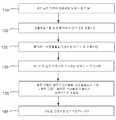
[0010]도 1은 개시된 실시예들에 따른 실리콘 산화물 선택적 에칭 프로세스의 흐름도이다.
[0011]도 2a는 본 발명의 실시예들에 따른 기판 프로세싱 챔버를 나타낸다.
[0012]도 2b는 본 발명의 실시예들에 따른 기판 프로세싱 챔버의 샤워헤드를 나타낸다.
[0013]도 3은 본 발명의 실시예들에 따른 기판 프로세싱 시스템을 나타낸다.
[0014]첨부된 도면들에서, 유사한 컴포넌트들 및/또는 피쳐들은 동일한 참조 부호(reference label)를 가질 수 있다. 또한, 동일한 유형의 다양한 컴포넌트들은, 유사한 컴포넌트들을 구별하는 제 2 부호 및 대시를 참조 부호에 뒤따르게 함으로써, 구별될 수 있다. 만일 본 명세서에서 제 1 참조 부호만이 사용되는 경우, 제 2 참조 부호와는 무관하게, 동일한 제 1 참조 부호를 갖는 유사한 컴포넌트들 중 임의의 컴포넌트에 대해 설명이 적용될 수 있다.By referring to the rest of the specification and the drawings, a further understanding of the nature and advantages of the disclosed embodiments may be realized.
1 is a flow chart of a silicon oxide selective etching process according to disclosed embodiments.
2A shows a substrate processing chamber according to embodiments of the present invention.
2B shows a showerhead in a substrate processing chamber according to embodiments of the present invention.
3 shows a substrate processing system according to embodiments of the present invention.
In the accompanying drawings, similar components and / or features may have the same reference label. Also, various components of the same type can be distinguished by following a reference code with a dash and a second code that distinguishes similar components. If only the first reference numeral is used herein, the description may be applied to any component among similar components having the same first reference numeral, regardless of the second reference numeral.
[0015]패터닝된 이종 구조들 상의 노출된 실리콘 산화물을 에칭하는 방법이 설명되며, 원격 플라즈마 에칭으로부터 생성되는 기상 에칭을 포함한다. 원격 플라즈마는 불소-함유 전구체를 여기시킨다. 원격 플라즈마로부터의 플라즈마 배출물들은 기판 프로세싱 영역 내로 유동되며, 기판 프로세싱 영역에서 플라즈마 배출물들은 수증기와 결합한다. 이에 의해 생성된 반응물질들은, 상이한 실리콘 산화물의 2개의 분리된 영역들을 제거하기 위해서, 패터닝된 이종 구조들을 상이한 에칭 속도들로 에칭한다. 방법들은, 고 밀도의 실리콘 산화물을 더 적게 제거하면서 저밀도의 실리콘 산화물을 제거하는 데에 사용될 수 있다.A method of etching exposed silicon oxide on patterned heterostructures is described, including gas phase etching resulting from remote plasma etching. The remote plasma excites the fluorine-containing precursor. Plasma emissions from the remote plasma flow into the substrate processing region, where the plasma emissions combine with water vapor. The reactants produced thereby etch the patterned heterogeneous structures at different etch rates to remove two separate regions of different silicon oxide. The methods can be used to remove low density silicon oxide while removing less high density silicon oxide.
[0016]선택적인 원격 기상 에칭 프로세스들은 암모니아(NH3)의 수소 소스 및 삼불화질소(NF3)의 불소 소스를 이용하였으며, 이들은 원격 플라즈마 시스템(RPS)을 통해 반응 영역 내로 함께 유동된다. 전형적으로, 암모니아 및 삼불화질소의 유량들은, 이러한 2개의 프로세스 가스들의 성분들을 효율적으로 이용하기 위해 수소의 원자 유량이 불소의 원자 유량의 대략 두배가 되도록 선택된다. 수소 및 불소의 존재는 비교적 낮은 기판 온도들에서 (NH4)2SiF6의 고체 부산물들의 형성을 가능하게 한다. 이러한 고체 부산물들은 기판의 온도를 승화(sublimation) 온도보다 높게 올림으로써 제거된다. 원격 기상 에칭 프로세스들은, 예를 들어 실리콘보다 훨씬 더 빠르게 산화물 필름들을 제거한다. 하지만, 실리콘 산화물의 상이한 제조들(preparations) 간의 에칭 속도들 사이에는 매우 적은 차이만 있다. 본 발명자들은, 원격 플라즈마에서 불소-함유 전구체를 여기시키고, 원격 플라즈마 시스템을 통과하지 않은 수증기와 플라즈마 배출물들을 결합함으로써, 고밀도 실리콘 산화물에 대한 저밀도 실리콘 산화물의 선택성이 강화될 수 있다는 것을 발견하였다.Optional remote gas phase etching processes used a hydrogen source of ammonia (NH3 ) and a fluorine source of nitrogen trifluoride (NF3 ), which flow together into the reaction zone through a remote plasma system (RPS). Typically, the flow rates of ammonia and nitrogen trifluoride are selected such that the atomic flow rate of hydrogen is approximately twice the atomic flow rate of fluorine to efficiently utilize the components of these two process gases. The presence of hydrogen and fluorine allows the formation of solid byproducts of (NH4 )2 SiF6 at relatively low substrate temperatures. These solid by-products are removed by raising the temperature of the substrate above the sublimation temperature. Remote gas phase etching processes remove oxide films much faster than, for example, silicon. However, there is only a very small difference between the etch rates between different preparations of silicon oxide. The inventors have found that the selectivity of low-density silicon oxide to high-density silicon oxide can be enhanced by exciting the fluorine-containing precursor in the remote plasma and combining plasma emissions with water vapor that has not passed through the remote plasma system.
[0017]본 발명을 더 잘 이해하고 인식하기 위해, 이제, 개시된 실시예들에 따른 실리콘 산화물 선택적 에칭 프로세스의 흐름도인 도 1을 참조한다. 제 1 동작 이전에, 기판은 패터닝되고 고밀도 실리콘 산화물이 패터닝된 기판 상에 증착된다. 그런 다음 저밀도 실리콘 산화물이 고밀도 실리콘 산화물 위에 증착되어, 예를 들어, 정교한 수직 피쳐를 위한 임시 희생 지지 구조로서 작용한다. 일단 저밀도 실리콘 산화물의 구조적 양태들이 더이상 필요하지 않으면, 본원에 설명된 에칭 프로세스를 이용하여, 고밀도 실리콘 산화물은 남겨두면서, 저밀도 실리콘 산화물은 제거될 수 있다.[0017] To better understand and recognize the present invention, reference is now made to FIG. 1, which is a flow diagram of a silicon oxide selective etching process according to disclosed embodiments. Prior to the first operation, the substrate is patterned and high density silicon oxide is deposited on the patterned substrate. The low density silicon oxide is then deposited over the high density silicon oxide, acting as a temporary sacrificial support structure for e.g. elaborate vertical features. Once the structural aspects of the low density silicon oxide are no longer needed, the low density silicon oxide can be removed while leaving the high density silicon oxide using the etching process described herein.
[0018]그런 다음, 패터닝된 기판은 프로세싱 영역으로 전달된다(동작 110). 프로세싱 영역으로부터 분리된 플라즈마 영역 내로의 삼불화질소의 유동이 시작된다(동작 120). 삼불화질소를 보강(augment)하거나 대체하기 위해 다른 불소 소스들이 사용될 수 있다. 일반적으로, 불소-함유 전구체가 플라즈마 영역 내로 유동될 수 있고, 불소-함유 전구체는 원자 불소, 이원자 불소, 삼불화질소, 사불화 탄소, 불화수소 및 이불화제논으로 이루어진 그룹으로부터 선택되는 적어도 하나의 전구체를 포함한다. 분리된 플라즈마 영역은 본원에서 원격 플라즈마 영역으로서 지칭될 수 있으며, 프로세싱 챔버와 별개의 모듈 또는 프로세싱 챔버 내의 격실(compartment) 내에 있을 수 있다. 그런 다음, 원격 플라즈마 영역에서 형성된 플라즈마 배출물들이 기판 프로세싱 영역 내로 유동된다(동작 125). 수증기가 기판 프로세싱 영역 내로 동시에 유동되어(동작 130), 플라즈마 배출물들과 반응한다. 수증기는 원격 플라즈마 영역을 통과하지 않으며, 이에 따라 플라즈마 배출물들과의 상호작용에 의해서만 여기된다. 본 발명의 실시예들에서, 수증기는, 기판 프로세싱 영역에 들어가기 전에 어떠한 원격 플라즈마 영역도 통과하지 않는다.The patterned substrate is then transferred to the processing region (act 110). The flow of nitrogen trifluoride into the plasma region separated from the processing region begins (operation 120). Other fluorine sources can be used to augment or replace nitrogen trifluoride. Generally, the fluorine-containing precursor can be flowed into the plasma region, and the fluorine-containing precursor is at least one selected from the group consisting of atomic fluorine, diatomic fluorine, nitrogen trifluoride, carbon tetrafluoride, hydrogen fluoride and non-fluorinated fluoride. Precursors. The separated plasma region may be referred to herein as a remote plasma region, and may be in a module separate from the processing chamber or within a compartment within the processing chamber. Plasma emissions formed in the remote plasma region are then flowed into the substrate processing region (act 125). Water vapor simultaneously flows into the substrate processing region (act 130) and reacts with the plasma emissions. Water vapor does not pass through the remote plasma region and is thus excited only by interaction with plasma emissions. In embodiments of the present invention, water vapor does not pass through any remote plasma region before entering the substrate processing region.
[0019]패터닝된 기판은, 저밀도 실리콘 산화물이 고밀도 실리콘 산화물보다 상당히 더 높은 속도로 제거되도록 선택적으로 에칭된다(동작 135). 이러한 능력은, 하나의 실리콘 산화물 영역(저밀도 실리콘 산화물)을 희생 컴포넌트로서 사용하는 동시에 또다른 실리콘 산화물 영역(고밀도 실리콘 산화물)은 노출되는 것을 가능하게 한다. 반응성 화학 종이 기판 프로세싱 영역으로부터 제거되고 그런 다음 기판이 프로세싱 영역으로부터 제거된다(동작 145).[0019] The patterned substrate is selectively etched such that low density silicon oxide is removed at a significantly higher rate than high density silicon oxide (operation 135). This ability makes it possible to use one silicon oxide region (low density silicon oxide) as a sacrificial component while exposing another silicon oxide region (high density silicon oxide). The reactive chemical paper is removed from the substrate processing region and then the substrate is removed from the processing region (act 145).
[0020]버퍼링된 산화물 에칭들(buffered oxide etches)과 같은 습식 에칭들이, 고밀도 실리콘 산화물에 비해 저밀도 실리콘 산화물을 선택적으로 제거하는 데에 또한 사용되었다. 본 발명자들은, 선택성이 약 6:1 또는 7:1(저밀도 SiO 에칭 속도:고밀도 SiO 에칭 속도)로 제한되었음을 발견하였다. 본원에 설명된 기상 건식 에칭 프로세스들을 사용할 때, 본 발명자들은, 40:1 및 심지어 50:1(저밀도 SiO 에칭 속도:고밀도 SiO 에칭 속도)의 선택성들이 가능하다는 것을 밝혀냈다(established). 본 발명의 실시예들에서, 저-밀도 실리콘 산화물 에칭 속도는 고-밀도 실리콘 산화물 에칭 속도를 약 8 또는 그 초과, 약 10 또는 그 초과, 약 15 또는 그 초과, 또는 약 25 또는 그 초과의 배수 인자(multiplicative factor)만큼 초과한다.Wet etches, such as buffered oxide etches, have also been used to selectively remove low density silicon oxide compared to high density silicon oxide. We have found that selectivity is limited to about 6: 1 or 7: 1 (low density SiO etch rate: high density SiO etch rate). When using the vapor phase dry etching processes described herein, the inventors have found that selectivities of 40: 1 and even 50: 1 (low density SiO etch rate: high density SiO etch rate) are possible. In embodiments of the present invention, the low-density silicon oxide etch rate is a multiple of a high-density silicon oxide etch rate of about 8 or greater, about 10 or greater, about 15 or greater, or about 25 or greater. It is exceeded by a multiplicative factor.
[0021]저밀도 실리콘 산화물을 초래하는 예시적인 증착 기술들은 디클로로실란을 증착 전구체로서 사용하는 화학 기상 증착, 스핀-온 글라스(SOG) 또는 플라즈마-강화형 화학 기상 증착을 포함한다. 본 발명의 실시예들에서, 고밀도 실리콘 산화물은 열 산화물(실리콘을, 예를 들어, 고온에서 O2에 노출시킴), 디실란 전구체 노(furnace) 산화 또는 고-밀도 플라즈마 화학 기상 증착으로서 증착될 수 있다.Exemplary deposition techniques resulting in low density silicon oxide include chemical vapor deposition, spin-on glass (SOG) or plasma-enhanced chemical vapor deposition using dichlorosilane as the deposition precursor. In embodiments of the present invention, high density silicon oxide is deposited as thermal oxide (exposing silicon to O2 at high temperature, for example), disilane precursor furnace oxidation or high-density plasma chemical vapor deposition. You can.
[0022]오직 불소만 (원격으로 또는 로컬로) 수반하는 기상 에칭들은, 패터닝된 기판의 (고-밀도 실리콘 산화물로 만들어진) 다른 부분들을 거의 그대로 (nearly undisturbed) 남겨두면서 저-밀도 실리콘 산화물을 제거하기 위해 필요한 선택성을 갖지 않는다. 본원에 설명된 기상 에칭들은, 고체 잔류물을 생성하지 않는다는 점에서, 부가된 이익을 갖는다. 고체 잔류물의 제거는, 희생 저밀도 실리콘 산화물에 의해서 지지될 수 있는 정밀한 피쳐들을 건드리는 것을 회피한다. 고체 잔류물의 제거는 또한, 프로세스 흐름들을 간략화하고, 승화 단계를 제거함으로써 프로세싱 비용들을 감소시킨다. 본 발명의 실시예들에서, 불소-함유 전구체에는 수소가 없다. 원격 플라즈마 영역에 수소 전구체들이 포함되지 않는 경우, 플라즈마 배출물들에 또한, 수소가 없을 수 있다. 이는, 패터닝된 기판 상에 고체 부산물들의 생성 가능성이 없음을 보장한다.Vapor etches involving only fluorine (remotely or locally) remove low-density silicon oxide while leaving other parts (made of high-density silicon oxide) of the patterned substrate almost undisturbed (nearly undisturbed). It does not have the selectivity needed to do it. The gas phase etchings described herein have added benefits in that they do not produce solid residues. Removal of the solid residue avoids touching precise features that can be supported by sacrificial low density silicon oxide. Removal of solid residues also reduces processing costs by simplifying process flows and eliminating sublimation steps. In embodiments of the present invention, the fluorine-containing precursor is hydrogen free. If hydrogen precursors are not included in the remote plasma region, the plasma emissions may also be hydrogen free. This ensures that there is no possibility of formation of solid by-products on the patterned substrate.
[0023]완전히 정확하거나(correct) 정확하지 않을 수도 있는 이론적인 메커니즘들에 청구항들의 적용 범위를 구속하는 것을 원하는 것은 아니지만, 가능한 메커니즘들의 일부 논의가 유익한 것으로 판명될 수 있다. 불소-함유 전구체를 원격 플라즈마 영역 내로 전달함으로써, 라디칼-불소(radical-fluorine) 전구체들이 생성된다. 본 출원인들은, 불소 이온들 및 원자들의 농도(concentration)가 생성되어 기판 프로세싱 영역 내로 전달된다고 가정한다. 수증기(H2O)는 불소와 반응하여, HF2- 와 같은 덜 반응적인 종을 생성할 수 있는데, 이러한 종은 패터닝된 기판 표면으로부터 저밀도 실리콘 산화물은 여전히 쉽게 제거하지만, 고밀도 실리콘 산화물은 쉽게 제거하지 않는다. 고체 잔류 부산물들의 결여와 결합되는 선택성은, 이들 에칭 프로세스들을, 남아있는 정교한 구조들에 변형을 거의 야기하지 않으면서, 정교한 비-실리콘 산화물 물질들로부터 몰드들 및 다른 실리콘 산화물 지지 구조들을 제거하는 데에 꽤 적합하게 한다.While not wishing to limit the scope of the claims to theoretical mechanisms that may or may not be completely correct, some discussion of possible mechanisms may prove beneficial. By delivering the fluorine-containing precursor into the remote plasma region, radical-fluorine precursors are produced. Applicants assume that concentrations of fluorine ions and atoms are generated and transferred into the substrate processing region. Water vapor (H2 O) can react with fluorine to produce less reactive species, such as HF2− , which still easily remove low density silicon oxide from the patterned substrate surface, but easily remove high density silicon oxide. I never do that. The selectivity combined with the lack of solid residual by-products helps these etch processes remove molds and other silicon oxide support structures from sophisticated non-silicon oxide materials with little or no strain on the remaining fine structures. It does quite well.
[0024]개시된 실시예들에서, 에칭 동작 동안, 기판 프로세싱 영역의 압력은 약 0.1Torr 또는 그 초과 및 약 50Torr 또는 그 미만일 수 있다. 개시된 실시예들에서, 기판 프로세싱 영역 내의 압력은 또한, 약 40Torr 또는 그 미만 및 약 5Torr 또는 그 초과 또는 10Torr일 수 있다. 상한들 중 임의의 상한은 이러한 하한들 중 임의의 하한과 결합되어 본 발명의 부가적인 실시예들을 형성할 수 있다. 개시된 실시예들에서, 에칭 동작 동안, 패터닝된 기판의 온도는 약 0℃ 또는 그 초과 및 약 100℃ 또는 그 미만일 수 있다. 본 발명의 실시예들에서, 에칭 동작 동안, 패터닝된 기판의 온도는 약 5℃ 또는 그 초과 및 약 40℃ 또는 그 미만일 수 있다.[0024] In the disclosed embodiments, during the etching operation, the pressure in the substrate processing region may be about 0.1 Torr or more and about 50 Torr or less. In the disclosed embodiments, the pressure in the substrate processing region may also be about 40 Torr or less and about 5 Torr or more or 10 Torr. Any of the upper limits can be combined with any of these lower limits to form additional embodiments of the invention. In the disclosed embodiments, during the etching operation, the temperature of the patterned substrate may be about 0 ° C or higher and about 100 ° C or lower. In embodiments of the present invention, during the etching operation, the temperature of the patterned substrate may be about 5 ° C or higher and about 40 ° C or lower.
[0025]예시적인 프로세싱 챔버와 시스템을 설명하는 동안, 부가적인 수증기 및 원격으로-여기된-불소 에칭 프로세스 파라미터들이 개시된다.[0025] While describing an exemplary processing chamber and system, additional water vapor and remotely-excited-fluorine etch process parameters are disclosed.
예시적인 프로세싱 시스템Exemplary processing system
[0026]본 발명의 실시예들을 구현할 수 있는 프로세싱 챔버들은 캘리포니아 산타 클라라의 어플라이드 머티어리얼스 인코포레이티드로부터 입수할 수 있는, CENTURA® 및 PRODUCER® 시스템들과 같은 프로세싱 플랫폼들 내부에 포함될 수 있다. 본 발명의 예시적인 방법들과 함께 사용될 수 있는 기판 프로세싱 챔버들의 예들은, "PROCESS CHAMBER FOR DIELECTRIC GAPFILL" 라는 명칭으로 2006년 5월 30일에 출원되었으며 본원과 양수인이 동일한, Lubomirsky 외의, 미국 가특허 출원 제 60/803,499 호에 도시되고 개시된 것들을 포함할 수 있고, 이의 전체 내용들은 모든 목적들을 위해 인용에 의해 본원에 포함된다. 추가의 예시적인 시스템들은, 미국 특허 제 6,387,207 호 및 제 6,830,624 호에 도시되고 개시된 것들을 포함할 수 있고, 이들 또한 모든 목적들을 위해 인용에 의해 본원에 포함된다.Processing chambers capable of implementing embodiments of the invention may be included within processing platforms such as CENTURA® and PRODUCER® systems, available from Applied Materials, Inc. of Santa Clara, California. have. Examples of substrate processing chambers that can be used with the exemplary methods of the present invention, filed May 30, 2006 under the designation "PROCESS CHAMBER FOR DIELECTRIC GAPFILL", have the same assignee as this application, other than Lubomirsky, US Provisional Patent May include those shown and disclosed in Application No. 60 / 803,499, the entire contents of which are incorporated herein by reference for all purposes. Additional exemplary systems may include those shown and disclosed in US Pat. Nos. 6,387,207 and 6,830,624, which are also incorporated herein by reference for all purposes.
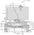
[0027]도 2a는 개시된 실시예들에 따른 기판 프로세싱 챔버(1001)이다. 원격 플라즈마 시스템(RPS)(1010)은 불소-함유 전구체를 프로세싱할 수 있으며, 이러한 불소-함유 전구체는 이후 가스 유입 조립체(gas inlet assembly)(1011)를 통해 이동한다. 2개의 분리된 가스 공급 채널들을 가스 유입 조립체(1011) 내에서 볼 수 있다. 제 1 채널(1012)은 원격 플라즈마 시스템(RPS)(1010)을 통과하는 가스를 운반하는 반면, 제 2 채널(1013)은 RPS(1010)를 바이패싱한다. 실시예들에서, 어느 채널이든 불소-함유 전구체를 위해 사용될 수 있다. 한편, 제 1 채널(1012)은 프로세스 가스를 위해 사용될 수 있고, 제 2 채널(1013)은 트리트먼트 가스(treatment gas)를 위해 사용될 수 있다. 덮개(1021)(예를 들어, 전도성 상단부 부분)와 천공된 격벽(perforated partition)(샤워헤드, 1053)이 이들 사이의 절연링(1024)과 함께 도시되어 있으며, 절연링은 AC 전위가 샤워헤드(1053)에 대해서 덮개(1021)에 인가될 수 있게 한다. AC 전위는 챔버 플라즈마 영역(1020)에서 플라즈마를 타격한다(strike). 프로세스 가스는 제 1 채널(1012)을 통해 챔버 플라즈마 영역(1020) 내로 이동할 수 있으며, 챔버 플라즈마 영역(1020)에서 플라즈마에 의해 단독으로, 또는 RPS(1010)와 조합하여 여기될 수 있다. 프로세스 가스(불소-함유 전구체)가 제 2 채널(1013)을 통해 유동하면, 챔버 플라즈마 영역(1020)만이 여기를 위해 사용된다. 챔버 플라즈마 영역(1020) 및/또는 RPS(1010)의 조합은 본 명세서에서 원격 플라즈마 시스템으로 지칭될 수 있다. (또한 '샤워헤드'라고도 지칭되는) 천공된 격벽(1053)은 챔버 플라즈마 영역(1020)을 샤워헤드(1053) 아래의 기판 프로세싱 영역(1070)으로부터 분리시킨다. 샤워헤드(1053)는 챔버 플라즈마 영역(1020) 내에 존재하는 플라즈마가 기판 프로세싱 영역(1070) 내의 가스들을 직접 여기시키지 않도록 하는 한편, 여기된 종이 챔버 플라즈마 영역(1020)으로부터 기판 프로세싱 영역(1070) 내로 여전히 이동할 수 있게 한다.2A is a
[0028]샤워헤드(1053)는 챔버 플라즈마 영역(1020)과 기판 프로세싱 영역(1070) 사이에 위치되며, RPS(1010) 및/또는 챔버 플라즈마 영역(1020) 내에서 생성되는 플라즈마 배출물들(전구체들 또는 다른 가스들의 여기된 유도체들)로 하여금, 판(plate)의 두께를 횡단하는 복수의 관통-홀들(1056)을 통과할 수 있도록 허용한다. 또한, 샤워헤드(1053)는 하나 또는 그 초과의 빈 용적들(hollow volumes)(1051)을 가지며, 이러한 용적들은 증기 또는 가스 형태의 전구체(이를 테면, 실리콘-함유 전구체)로 충진될 수 있고, 작은 홀들(1055)을 통해 기판 프로세싱 영역(1070) 내로 통과하지만, 챔버 플라즈마 영역(1020) 내로는 직접 통과되지 않는다. 개시된 본 실시예에서, 샤워헤드(1053)는 관통-홀들(1056)의 최소 직경(1050)의 길이보다 더 두껍다. 챔버 플라즈마 영역(1020)으로부터 기판 프로세싱 영역(1070)으로 침투(penetrate)하는 여기된 종의 상당한(significant) 농도를 유지하기 위해, 관통-홀들의 최소 직경(1050)의 길이(1026)는 샤워헤드(1053)를 관통하는 중간에 관통-홀들(1056)의 더 큰 직경 부분들을 형성함으로써 제한될 수 있다. 개시된 실시예들에서, 관통-홀들(1056)의 최소 직경(1050)의 길이는 관통-홀들(1056)의 최소 직경과 동일한 자릿수(same order of magnitude)이거나 그보다 작을 수 있다.The
[0029]도시된 실시예에서, 샤워헤드(1053)는 산소, 수소 및/또는 질소를 포함하는 프로세스 가스들, 및/또는 챔버 플라즈마 영역(1020)에서 플라즈마에 의해 여기될 때 그러한 프로세스 가스들의 플라즈마 배출물을 (관통-홀들(1056)을 통해) 분배할 수 있다. 실시예들에서, 제 1 채널(1012)을 통해 챔버 플라즈마 영역(1020) 내로 및/또는 RPS(1010) 내로 유입되는 프로세스 가스는 불소(예컨대, CF4, NF3 또는 XeF2)를 포함할 수 있다. 또한, 프로세스 가스는 헬륨, 아르곤, 질소(N2) 등과 같은 캐리어 가스를 포함할 수 있다. 플라즈마 배출물들은, 프로세스 가스의 이온화된 또는 중성의 유도체들을 포함할 수 있으며, 유입된 프로세스 가스의 원자 성분에 관련되는 라디칼-불소 전구체로서 본 명세서에서 또한 지칭될 수 있다.In the illustrated embodiment, the
[0030]실시예들에서, 관통-홀들(1056)의 개수는 약 60 내지 약 2000개일 수 있다. 관통-홀들(1056)은 다양한 형상들을 가질 수 있으나, 가장 용이하게는 원형으로 제조된다. 개시된 실시예들에서, 관통-홀들(1056)의 최소 직경(1050)은 약 0.5㎜ 내지 약 20㎜이거나, 약 1㎜ 내지 약 6㎜일 수 있다. 또한, 관통-홀들의 단면 형상을 자유롭게 선택할 수 있으며, 단면 형상은 원뿔형, 원통형 또는 이 두가지 형상들의 조합으로 제조될 수 있다. 기판 프로세싱 영역(1070) 내로 가스를 유입시키는 데에 사용되는 작은 홀들(1055)의 개수는, 상이한 실시예들에서, 약 100 내지 약 5000개이거나, 또는 약 500 내지 약 2000개일 수 있다. 작은 홀들(1055)의 직경은 약 0.1㎜ 내지 약 2㎜일 수 있다.In embodiments, the number of through-
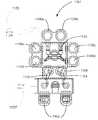
[0031]도 2b는 개시된 실시예들에 따른 프로세싱 챔버와 함께 사용하기 위한 샤워헤드(1053)의 저면도이다. 샤워헤드(1053)는 도 2a에 도시된 샤워헤드에 대응한다. 관통-홀들(1056)은 샤워헤드(1053)의 바닥에서 더 큰 내부 직경(ID)을 갖고 상단에서 더 작은 ID를 갖는 것으로 도시되어 있다. 작은 홀들(1055)이 샤워헤드의 표면에 걸쳐, 심지어는 관통-홀들(1056) 사이에서도 실질적으로 균일하게 분포됨으로써, 본 명세서에 설명되는 다른 실시예들보다 더 균일한 혼합을 제공하는 것을 돕는다. 수증기가 이중-구역 샤워헤드의 분리된 구역들을 통과하여 작은 홀들(1055)을 통해 기판 프로세싱 영역으로 들어가는 동안, 불소-함유 전구체는 이중-구역(dual-zone) 샤워헤드(1053)의 관통-홀들(1056)을 통해서 유동될 수 있다. 분리된 구역들은 기판 프로세싱 영역 내로는 개방되지만 원격 플라즈마 영역 내로는 개방되지 않는다.2B is a bottom view of a
[0032]샤워헤드(1053) 내의 관통-홀들(1056)을 통해 도달하는 불소-함유 플라즈마 배출물들이, 빈 용적들(1051)로부터 비롯되는 작은 홀들(1055)을 통해 도달하는 수분과 결합할 때, 예시적인 패터닝된 기판은 기판 프로세싱 영역(1070) 내부의 페디스털(pedestal)(미도시)에 의해 지지될 수 있다. 비록 기판 프로세싱 영역(1070)이 경화(curing)와 같은 다른 프로세스들을 위해 플라즈마를 지원하도록 설비될 수 있기는 하지만, 본 발명의 실시예들에서는, 패터닝된 기판을 에칭하는 동안 어떠한 플라즈마도 존재하지 않는다.When the fluorine-containing plasma emissions reaching through the through-
[0033]플라즈마는 샤워헤드(1053) 위의 챔버 플라즈마 영역(1020) 또는 샤워헤드(1053) 아래의 기판 프로세싱 영역(1070) 중 어느 하나에서 점화될 수 있다. 불소-함유 전구체의 유입(inflow)으로부터 라디칼-불소 전구체들을 생성하기 위해 플라즈마가 챔버 플라즈마 영역(1020)에 존재한다. 증착 동안 챔버 플라즈마 영역(1020)에서 플라즈마를 점화하기 위해, 통상적으로 무선 주파수(RF) 범위의 AC 전압이 샤워헤드(1053)와 프로세싱 챔버의 전도성 상단부 부분(1021) 사이에 인가된다. RF 전력 공급부는 13.56㎒의 높은 RF 주파수를 발생시키지만, 또한 다른 주파수들을 단독으로 또는 13.56㎒ 주파수와 조합하여 발생시킬 수 있다.Plasma may be ignited in either the
[0034]기판 프로세싱 영역(1070)과 접한 내부 표면들을 세정(clean)하기 위해 기판 프로세싱 영역(1070)에서 하위 플라즈마(bottom plasma)가 턴온(turn on)될 때, 상위 플라즈마(top plasma)는 저전력 또는 무전력으로 유지될 수 있다. 기판 프로세싱 영역(1070) 내의 플라즈마는, 샤워헤드(1053)와 챔버의 페디스털 또는 바닥 사이에 AC 전압을 인가함으로써 점화된다. 플라즈마가 존재하는 동안, 세정 가스(cleaning gas)가 기판 프로세싱 영역(1070) 내로 유입될 수 있다.[0034] When the bottom plasma is turned on in the
[0035]페디스털은 열 교환 채널을 가질 수 있으며, 이러한 열 교환 채널을 통해 열 교환 유체가 유동하여 기판의 온도를 제어한다. 이러한 구성은 기판 온도가 비교적 저온들(실온 내지 약 120℃)로 유지되도록 냉각 또는 가열될 수 있도록 한다. 열 교환 유체는 에틸렌 글리콜과 물을 포함할 수 있다. 또한, 페디스털(바람직하게는, 알루미늄, 세라믹, 또는 이들의 조합)의 웨이퍼 지지 플래터(platter)는, 평행한 동심원들의 형태로 2개의 완전한 턴들(turns)을 만들도록 구성된 내장형의 단일 루프 내장식 히터 엘리먼트를 사용하여 비교적 고온들(약 120℃ 내지 약 1100℃)을 달성하기 위해 저항식으로 가열될 수 있다. 히터 엘리먼트의 외측 부분은 지지 플래터의 주변 근처에서 연장될 수 있는 반면, 내측 부분은 더 작은 반경을 가진 동심원의 경로 상에서 연장된다. 히터 엘리먼트에 대한 배선은 페디스털의 스템(stem)을 통과한다.The pedestal may have a heat exchange channel, through which the heat exchange fluid flows to control the temperature of the substrate. This configuration allows the substrate temperature to be cooled or heated to be maintained at relatively low temperatures (room temperature to about 120 ° C). The heat exchange fluid can include ethylene glycol and water. In addition, the wafer support platter of the pedestal (preferably aluminum, ceramic, or a combination thereof) is in a built-in single loop configured to make two complete turns in the form of parallel concentric circles. The decorative heater element can be used to heat resistively to achieve relatively high temperatures (about 120 ° C to about 1100 ° C). The outer part of the heater element can extend near the periphery of the support platter, while the inner part extends on a concentric path with a smaller radius. The wiring to the heater element passes through the pedestal stem.
[0036]기판 프로세싱 시스템은 시스템 제어기에 의해 제어된다. 예시적인 실시예에서, 시스템 제어기는 하드 디스크 드라이브, 플로피 디스크 드라이브 및 프로세서를 포함한다. 프로세서는 싱글-보드 컴퓨터(SBC), 아날로그 및 디지털 입/출력 보드들, 인터페이스 보드들 및 스텝퍼 모터 제어기 보드들을 포함한다. CVD 시스템의 다양한 부분들은, 보드, 카드 케이지 및 커넥터 치수들 및 타입들을 정의하는 VME(Versa Modular European) 표준을 따른다. 이러한 VME 표준은 또한 버스 구조를 16-비트 데이터 버스 및 24-비트 어드레스 버스를 갖는 것으로서 정의한다.[0036] The substrate processing system is controlled by a system controller. In an exemplary embodiment, the system controller includes a hard disk drive, floppy disk drive, and processor. The processor includes a single-board computer (SBC), analog and digital input / output boards, interface boards and stepper motor controller boards. The various parts of the CVD system conform to the Versa Modular European (VME) standard that defines board, card cage and connector dimensions and types. This VME standard also defines the bus structure as having a 16-bit data bus and a 24-bit address bus.
[0037]시스템 제어기는 에칭 챔버의 모든 활동들(activities)을 제어한다. 시스템 제어기는, 컴퓨터-판독가능한 매체에 저장되어 있는 컴퓨터 프로그램인 시스템 제어 소프트웨어를 실행한다. 바람직하게는, 매체는 하드 디스크 드라이브이지만, 이러한 매체는 또한 다른 종류들의 메모리일 수 있다. 컴퓨터 프로그램은 특정 프로세스의, 타이밍, 가스들의 혼합, 챔버 압력, 챔버 온도, RF 전력 레벨들, 서셉터 위치, 및 다른 파라미터들을 지시하는 명령어들의 세트들(sets)을 포함한다. 예를 들어, 플로피 디스크 또는 기타의 다른 적절한 드라이브를 포함하는 다른 메모리 디바이스들 상에 저장된 다른 컴퓨터 프로그램들이 또한 시스템 제어기에게 명령하는 데에 이용될 수 있다.The system controller controls all activities of the etching chamber. The system controller executes system control software, which is a computer program stored in a computer-readable medium. Preferably, the medium is a hard disk drive, but such medium may also be other types of memory. The computer program includes a set of instructions indicating the timing of a particular process, mixing of gases, chamber pressure, chamber temperature, RF power levels, susceptor location, and other parameters. Other computer programs stored on other memory devices, including, for example, a floppy disk or other suitable drive, can also be used to instruct the system controller.
[0038]기판 상에 저-밀도 실리콘 산화물과 고-밀도 실리콘 산화물을 차등적으로(differentially) 에칭하기 위한 프로세스 또는 챔버를 세정하기 위한 프로세스는 시스템 제어기에 의해 실행되는 컴퓨터 프로그램 제품을 사용하여 실시될 수 있다. 컴퓨터 프로그램 코드는 종래의 임의의 컴퓨터 판독가능한 프로그래밍 언어, 예를 들어 어셈블리 언어: C, C++, 파스칼, 포트란 또는 기타 언어들로 기록될 수 있다. 적합한 프로그램 코드가 통상의 텍스트 에디터를 사용하여 단일 파일 또는 다중 파일들에 입력되고, 컴퓨터의 메모리 시스템과 같은 컴퓨터 사용가능한 매체에 저장되거나 구현된다. 입력된 코드 텍스트가 고수준 언어라면, 코드는 컴파일된 다음, 결과적인 컴파일러 코드가 프리컴파일형(precompiled) Microsoft Windows® 라이브러리 루틴들의 목적 코드와 링크된다. 링크되는 컴파일된 목적 코드를 실행하기 위해, 시스템 사용자는 목적 코드를 호출하여, 컴퓨터 시스템으로 하여금 메모리에 코드를 로딩하게 한다. 그런 다음, CPU는 코드를 판독하고 실행하여, 프로그램에서 식별되는 과제들을 수행한다.[0038] The process for differentially etching low-density silicon oxide and high-density silicon oxide on the substrate or the process for cleaning the chamber may be implemented using a computer program product executed by a system controller. Can be. The computer program code can be written in any conventional computer readable programming language, for example assembly language: C, C ++, Pascal, Fortran or other languages. Suitable program code is entered into a single file or multiple files using a conventional text editor, and stored or implemented in a computer usable medium, such as a computer's memory system. If the code text entered is a high-level language, the code is compiled, and the resulting compiler code is then linked with the object code of the precompiled Microsoft Windows® library routines. To execute the compiled compiled object code, the system user calls the object code, causing the computer system to load the code into memory. The CPU then reads and executes the code to perform the tasks identified in the program.
[0039]사용자와 제어기 사이의 인터페이스는 평판(flat-panel) 터치 감응형 모니터를 통해 이루어진다. 바람직한 실시예에서는, 2개의 모니터들이 사용되는데, 하나는 작업자들을 위해 클린룸 벽에 장착되고, 다른 하나는 서비스 기술자들을 위해 벽 뒤에 장착된다. 이러한 2개의 모니터들은 동일한 정보를 동시에 디스플레이할 수 있는데, 이 경우, 한번에 단지 하나의 모니터만이 입력을 받아들인다. 특정 스크린 또는 기능을 선택하기 위해, 작업자는 터치 감응형 모니터의 지정된 영역을 터치한다. 터치된 영역은 자신의 하이라이트된 색을 변화시키거나, 새로운 메뉴 또는 스크린이 디스플레이되어, 작업자와 터치 감응형 모니터 간의 통신을 확인한다. 터치 감응형 모니터 대신에 또는 터치 감응형 모니터에 부가하여, 다른 디바이스들, 이를 테면 키보드, 마우스, 또는 다른 포인팅 또는 통신 디바이스가 이용되어, 사용자가 시스템 제어기와 통신할 수 있게 한다.The interface between the user and the controller is made through a flat-panel touch-sensitive monitor. In the preferred embodiment, two monitors are used, one mounted on the wall of a clean room for workers, and the other behind a wall for service technicians. These two monitors can display the same information simultaneously, in which case only one monitor at a time accepts input. To select a particular screen or function, the operator touches a designated area of the touch-sensitive monitor. The touched area changes its highlighted color, or a new menu or screen is displayed, confirming communication between the operator and the touch-sensitive monitor. Instead of or in addition to a touch-sensitive monitor, other devices, such as a keyboard, mouse, or other pointing or communication device, are used to allow the user to communicate with the system controller.
[0040]챔버 플라즈마 영역 또는 RPS 내의 영역은 원격 플라즈마 영역으로 지칭될 수 있다. 실시예들에서, 라디칼 전구체(예를 들어, 라디칼-불소 전구체)가 원격 플라즈마 영역에서 생성되고 기판 프로세싱 영역 내로 이동하여, 수증기와 결합한다. 실시예들에서, 수증기는 라디칼-불소 전구체(플라즈마 배출물들로도 알려진)에 의해서만 여기된다. 실시예들에서, 라디칼-불소 전구체가 수증기에 대해 우세한(dominant) 여기를 제공하는 것을 보장하기 위해, 플라즈마 전력은 본질적으로 챔버 플라즈마 영역에만 인가될 수 있다.[0040] The chamber plasma region or the region within the RPS may be referred to as a remote plasma region. In embodiments, a radical precursor (eg, a radical-fluorine precursor) is created in a remote plasma region and moved into a substrate processing region, where it is combined with water vapor. In embodiments, water vapor is excited only by a radical-fluorine precursor (also known as plasma emissions). In embodiments, plasma power may be applied essentially only to the chamber plasma region to ensure that the radical-fluorine precursor provides dominant excitation for water vapor.
[0041]챔버 플라즈마 영역을 사용하는 실시예들에서, 여기된 플라즈마 배출물들은 증착 영역으로부터 구획되는 기판 프로세싱 영역의 섹션에서 발생된다. 본 명세서에서 기판 프로세싱 영역으로 또한 알려져있는 증착 영역은, 패터닝된 기판(예를 들어, 반도체 웨이퍼)을 에칭하기 위해 플라즈마 배출물들이 수증기와 혼합되고 반응하는 곳이다. 여기된 플라즈마 배출물들은 또한 비활성 가스들(예시적인 경우, 아르곤)을 수반할 수 있다. 실시예들에서, 수증기는 기판 플라즈마 영역에 들어가기 전에 플라즈마를 통과하지 않는다. 기판 프로세싱 영역은, 패터닝된 기판의 에칭 동작 동안, 본 명세서에서 "무-플라즈마(plasma-free)"인 것으로서 설명될 수 있다. "무-플라즈마"는 영역에 플라즈마가 없다는 것을 반드시 의미하지는 않는다. 플라즈마 영역 내에서 생성되는 이온화된 종 및 자유 전자들은 구획(샤워헤드)의 구멍들(개구들)을 통해 이동하지만, 수증기는 플라즈마 영역에 인가되는 플라즈마 전력에 의해 실질적으로 여기되지 않는다. 챔버 플라즈마 영역에서의 플라즈마의 경계들은 정의하기 어렵고, 샤워헤드의 개구들을 통해 기판 프로세싱 영역을 침범할 수 있다. 유도적으로-결합된 플라즈마의 경우, 소량의 이온화가 직접적으로 기판 프로세싱 영역 내에서 이루어질 수 있다. 또한, 형성하는 필름의 바람직한 특징들을 없애지 않으면서, 기판 프로세싱 영역에서 저 강도(intensity)의 플라즈마가 생성될 수 있다. 여기된 플라즈마 배출물들을 생성하는 동안 챔버 플라즈마 영역(또는, 그 점에 대해서는, 원격 플라즈마 영역)보다 훨씬 더 낮은 강도의 이온 밀도를 갖는 플라즈마에 대한 모든 원인들(causes)은 본 명세서에 사용되는 바와 같은 "무-플라즈마"의 범위를 벗어나지 않는다.In embodiments using a chamber plasma region, excited plasma emissions are generated in a section of the substrate processing region that is partitioned from the deposition region. A deposition region, also known herein as a substrate processing region, is where plasma emissions mix and react with water vapor to etch a patterned substrate (eg, semiconductor wafer). The excited plasma emissions can also involve inert gases (argon in the exemplary case). In embodiments, water vapor does not pass through the plasma before entering the substrate plasma region. The substrate processing region may be described herein as being “plasma-free” during the etching operation of the patterned substrate. “Non-plasma” does not necessarily mean that there is no plasma in the region. Ionized species and free electrons generated in the plasma region travel through the holes (openings) of the compartment (showerhead), but water vapor is not substantially excited by the plasma power applied to the plasma region. The boundaries of the plasma in the chamber plasma region are difficult to define and can invade the substrate processing region through the openings in the showerhead. In the case of an inductively-coupled plasma, a small amount of ionization can be done directly within the substrate processing region. In addition, plasma of low intensity can be generated in the substrate processing region without removing the desirable characteristics of the film to be formed. While generating the excited plasma emissions, all the causes for plasma having an ionic density of much lower intensity than the chamber plasma region (or, in that respect, remote plasma region) are as used herein. It does not go beyond the scope of "no plasma".
[0042]삼불화질소(또는 다른 불소-함유 전구체)는, 상이한 실시예들에서, 약 25sccm 내지 약 200sccm, 약 50sccm 내지 약 150sccm, 또는 약 75sccm 내지 약 125sccm의 속도들로 챔버 플라즈마 영역(1020) 내로 유동될 수 있다. 수증기는, 상이한 실시예들에서, 약 25sccm 내지 약 200sccm, 약 50sccm 내지 약 150sccm, 또는 약 75sccm 내지 약 125sccm의 속도들로 기판 프로세싱 영역(1070) 내로 유동될 수 있다.Nitrogen trifluoride (or other fluorine-containing precursor), in different embodiments,
[0043]챔버 내로의 수증기 및 불소-함유 전구체의 조합된 유량들은 전체 가스 혼합물의 0.05용적% 내지 약 20용적%를 차지할 수 있으며, 나머지는 캐리어 가스들이다. 실시예들에서, 불소-함유 전구체가 원격 플라즈마 영역 내로 유동되지만, 플라즈마 배출물들은 동일한 용적 유동 비율을 갖는다. 불소-함유 전구체의 경우, 원격 플라즈마 영역 내의 압력을 안정화하기 위해, 불소-함유 가스의 개시 전에, 퍼지 가스 또는 캐리어 가스가 원격 플라즈마 영역 내로 먼저 개시될 수 있다.[0043] Combined flow rates of water vapor and fluorine-containing precursors into the chamber can occupy from 0.05% to about 20% by volume of the total gas mixture, the remainder being carrier gases. In embodiments, the fluorine-containing precursor flows into the remote plasma region, but the plasma emissions have the same volume flow rate. In the case of a fluorine-containing precursor, in order to stabilize the pressure in the remote plasma region, a purge gas or carrier gas may be first initiated into the remote plasma region prior to initiation of the fluorine-containing gas.
[0044]플라즈마 전력은 다양한 주파수들이거나 다중 주파수들의 조합일 수 있다. 예시적인 프로세싱 시스템에서, 플라즈마는 샤워헤드(1053)에 대하여 덮개(1021)에 전달되는 RF 전력에 의해 제공된다. 상이한 실시예들에서, RF 전력은 약 10 와트 내지 약 2000 와트, 약 100 와트 내지 약 2000 와트, 약 200 와트 내지 약 1500 와트, 또는 약 500 와트 내지 약 1000 와트일 수 있다. 상이한 실시예들에서, 예시적인 프로세싱 시스템에서 인가되는 RF 주파수는 약 200㎑ 미만의 낮은 RF 주파수들, 약 10㎒ 내지 약 15㎒의 높은 RF 주파수들, 또는 약 1㎓ 또는 그 초과의 극초단파(microwave) 주파수들일 수 있다. 플라즈마 전력은 원격 플라즈마 영역 내로 용량-결합(CCP)되거나 유도-결합(ICP)될 수 있다.Plasma power may be various frequencies or a combination of multiple frequencies. In the exemplary processing system, plasma is provided by the RF power delivered to the
[0045]수증기, 임의의 캐리어 가스들 및 플라즈마 배출물들이 기판 프로세싱 영역(1070) 내로 유동하는 동안, 기판 프로세싱 영역(1070)은 다양한 압력들로 유지될 수 있다. 상이한 실시예들에서, 압력은 약 500mTorr 내지 약 30Torr, 약 1Torr 내지 약 20Torr, 또는 약 5Torr 내지 약 15Torr로 유지될 수 있다.[0045] While water vapor, any carrier gases and plasma emissions flow into the
[0046]하나 또는 그 초과의 실시예들에서, 기판 프로세싱 챔버(1001)는 캘리포니아, 산타 클라라에 소재하는 어플라이드 머티어리얼스 인코포레이티드로부터 입수할 수 있는 ProducerTM GT, CenturaTM AP 및 EnduraTM 플랫폼들을 포함하는 다양한 멀티-프로세싱 플랫폼들 내에 통합될 수 있다. 이러한 프로세싱 플랫폼은 진공을 깨뜨리지 않으면서 여러개의 프로세싱 동작들을 수행할 수 있다. 본 발명의 실시예들을 구현할 수 있는 프로세싱 챔버들은, 다른 타입들의 챔버들 중에서도, 유전체 에칭 챔버들 또는 다양한 화학 기상 증착 챔버들을 포함할 수 있다.In one or more embodiments, the
[0047]증착 시스템들의 실시예들은 집적 회로 칩들을 생산하기 위한 더 큰 제조 시스템들에 통합될 수 있다. 도 3은 개시된 실시예들에 따른 증착, 베이킹(baking) 및 경화 챔버들의 그러한 하나의 시스템(1101)을 도시한다. 도면에서, 한 쌍의 FOUP들(front opening unified pods)(전면 개방형 통합 포드들)(1102)이 기판들(예컨대, 300㎜ 직경의 웨이퍼들)을 공급하며, 이러한 기판들은 로봇 암들(1104)에 의해 수용(receive)되고, 기판 프로세싱 챔버들(1108a-f) 중 하나 내에 배치되기 전에 저압의 홀딩 영역(1106) 내에 배치된다. 홀딩 영역(1106)으로부터 기판 프로세싱 챔버들(1108a-f)로 그리고 그 역으로 기판 웨이퍼들을 운반하기 위해, 제 2 로봇 암(1110)이 사용될 수 있다. 각각의 기판 프로세싱 챔버(1108a-f)는, 순환식 층 증착(cyclical layer deposition)(CLD), 원자 층 증착(ALD), 화학 기상 증착(CVD), 물리 기상 증착(PVD), 에칭, 예비 세정(pre-clean), 탈기(degas), 배향 및 다른 기판 프로세스들에 부가하여, 본 명세서에 설명된 건식 에칭 프로세스들을 포함하는 다수의 기판 프로세싱 동작들을 수행하도록 갖춰질 수 있다.Embodiments of deposition systems can be incorporated into larger manufacturing systems for producing integrated circuit chips. 3 shows one
[0048]기판 프로세싱 챔버들(1108a-f)은 기판 웨이퍼 상에 유동성 유전체 필름을 증착, 어닐링, 경화 및/또는 에칭하기 위한 하나 또는 그 초과의 시스템 구성요소들을 포함할 수 있다. 하나의 구성에서, 기판 상에 유전체 물질을 증착하기 위해 2쌍의 프로세싱 챔버(예를 들어, 1108c-d 및 1108e-f)가 사용될 수 있으며, 증착된 유전체를 에칭하기 위해 제 3 쌍의 프로세싱 챔버들(예를 들어, 1108a-b)이 사용될 수 있다. 다른 구성에서, 모든 3쌍의 챔버들(예를 들어, 1108a-f)은 기판 상의 유전체 필름을 에칭하도록 구성될 수 있다. 설명된 프로세스들 중 임의의 하나 또는 그 초과의 프로세스는, 상이한 실시예들에서, 도시된 제조 시스템으로부터 분리된 챔버(들)에서 실시될 수 있다.[0048] The
[0049]시스템 제어기(1157)는 모터들, 밸브들, 유동 제어기들, 전력 공급부들 및 본 명세서에 설명되는 프로세스 레시피들을 실시하기 위해 요구되는 다른 기능들을 제어하는 데에 사용된다. 기판 프로세싱 챔버들(1108a-f) 중 하나 또는 모두에 가스들을 유입하도록, 가스 핸들링 시스템(1155)이 또한 시스템 제어기(1157)에 의해 제어될 수 있다. 시스템 제어기(1157)는 가스 핸들링 시스템(1155) 및/또는 기판 프로세싱 챔버들(1108a-f) 내에서 이동가능한 기계 조립체들의 위치를 결정하고 조정하기 위하여 광학 센서들로부터의 피드백에 의존할 수 있다. 기계 조립체들은 시스템 제어기(1157)의 제어하에서 모터들에 의해 움직이는 서셉터들, 스로틀 밸브들 및 로봇을 포함할 수 있다.[0049] The
[0050]예시적인 실시예에서, 시스템 제어기(1157)는 하드 디스크 드라이브(메모리), USB 포트들, 플로피 디스크 드라이브 및 프로세서를 포함한다. 시스템 제어기(1157)는 아날로그 및 디지털 입/출력 보드들, 인터페이스 보드들 및 스텝퍼 모터 제어기 보드들을 포함한다. 프로세싱 챔버들(1108a-f)을 포함하는 멀티-챔버 프로세싱 시스템(1101)의 다양한 부분들은 시스템 제어기(1157)에 의해 제어된다. 시스템 제어기는 하드 디스크, 플로피 디스크 또는 플래시 메모리 썸(thumb) 드라이브와 같은 컴퓨터 판독가능한 매체에 저장된 컴퓨터 프로그램 형태의 시스템 제어 소프트웨어를 실행한다. 다른 타입들의 메모리가 또한 사용될 수 있다. 컴퓨터 프로그램은 특정 프로세스의, 타이밍, 가스들의 혼합, 챔버 압력, 챔버 온도, RF 전력 레벨들, 서셉터 위치, 및 다른 파라미터들을 지시하는 명령어들의 세트들을 포함한다.In an exemplary embodiment, the
[0051]기판 상에 필름을 에칭, 증착 또는 다른 처리를 하기 위한 프로세스 또는 챔버를 세정하기 위한 프로세스는, 제어기에 의해 실행되는 컴퓨터 프로그램 제품을 사용하여 실시될 수 있다. 컴퓨터 프로그램 코드는 종래의 임의의 컴퓨터 판독가능한 프로그래밍 언어: 예를 들어 어셈블리 언어, C, C++, 파스칼, 포트란 또는 기타 언어들로 기록될 수 있다. 적합한 프로그램 코드가 통상의 텍스트 에디터를 사용하여 단일 파일 또는 다중 파일들에 입력되고, 컴퓨터의 메모리 시스템과 같은 컴퓨터 사용가능한 매체에 저장되거나 구현된다. 입력된 코드 텍스트가 고수준 언어라면, 코드는 컴파일된 다음, 결과적인 컴파일러 코드가 프리컴파일형 Microsoft Windows® 라이브러리 루틴들의 목적 코드와 링크된다. 링크되는 컴파일된 목적 코드를 실행하기 위해, 시스템 사용자는 목적 코드를 호출하여, 컴퓨터 시스템으로 하여금 메모리에 코드를 로딩하게 한다. 그런 다음, CPU는 코드를 판독하고 실행하여, 프로그램에서 식별되는 과제들을 수행한다.[0051] The process for etching, depositing, or other processing of the film on the substrate or the process for cleaning the chamber may be performed using a computer program product executed by a controller. The computer program code can be written in any conventional computer readable programming language: assembly language, C, C ++, Pascal, Fortran or other languages. Suitable program code is entered into a single file or multiple files using a conventional text editor, and stored or implemented in a computer usable medium, such as a computer's memory system. If the code text entered is a high-level language, the code is compiled, and the resulting compiler code is then linked to the target code of the precompiled Microsoft Windows® library routines. To execute the compiled compiled object code, the system user calls the object code, causing the computer system to load the code into memory. The CPU then reads and executes the code to perform the tasks identified in the program.
[0052]사용자와 제어기 사이의 인터페이스는 터치 감응형 모니터를 통해 이루어질 수 있고, 마우스와 키보드를 또한 포함할 수 있다. 일 실시예에서는, 2개의 모니터들이 사용되는데, 하나는 작업자들을 위해 클린룸 벽에 장착되고, 다른 하나는 서비스 기술자들을 위해 벽 뒤에 장착된다. 이러한 2개의 모니터들은 동일한 정보를 동시에 디스플레이할 수 있는데, 이 경우, 한번에 단지 하나의 모니터만이 입력을 받아들이도록 구성된다. 특정 스크린 또는 기능을 선택하기 위해, 작업자는 손가락 또는 마우스로 디스플레이 스크린 상의 지정된 영역을 터치한다. 터치된 영역은 자신의 하이라이트된 색을 변화시키거나, 새로운 메뉴 또는 스크린이 디스플레이되어, 작업자의 선택을 확인한다.[0052] The interface between the user and the controller may be made through a touch-sensitive monitor, and may also include a mouse and keyboard. In one embodiment, two monitors are used, one mounted on the wall of a clean room for workers, and the other behind a wall for service technicians. These two monitors can simultaneously display the same information, in which case only one monitor at a time is configured to accept input. To select a particular screen or function, the operator touches a designated area on the display screen with a finger or mouse. The touched area changes its highlighted color, or a new menu or screen is displayed, confirming the operator's choice.
[0053]본 명세서에서 사용된 바와 같이, "기판"은 상부에 층들이 형성되거나 형성되지 않은 지지 기판일 수 있다. 패터닝된 기판은 다양한 도핑 농도들 및 프로파일들의 반도체 또는 절연체일 수 있으며, 예를 들어, 집적 회로들의 제조에 사용되는 타입의 반도체 기판일 수 있다. 패터닝된 기판의 노출된 "실리콘 산화물"은 주로 SiO2이지만, 질소, 수소, 탄소 등과 같은 다른 원소 성분들의 농도들을 포함할 수 있다. 몇몇 실시예들에서, 본 명세서에 개시된 방법들을 사용하여 에칭되는 실리콘 산화물 필름들은 본질적으로 실리콘과 산소로 이루어진다. 용어 "전구체"는 표면으로부터 물질을 제거하거나 표면 상에 물질을 증착하기 위해 반응에 참여하는 임의의 프로세스 가스를 나타내기 위해 사용된다. "플라즈마 배출물들"은 챔버 플라즈마 영역으로부터 빠져나와 기판 프로세싱 영역에 들어가는 가스를 설명한다. 플라즈마 배출물들은, 가스 분자들 중 적어도 일부가 진동 여기되거나, 해리되거나(dissociated) 및/또는 이온화된 상태인 "여기된 상태"에 있다. "라디칼 전구체"는 표면으로부터 물질을 제거하거나 표면 상에 물질을 증착하기 위해 반응에 참여하는 플라즈마 배출물들(플라즈마를 빠져나가는 여기된 상태의 가스)을 설명하는데 사용된다. "라디칼-불소 전구체"는 불소를 함유하는 라디칼 전구체이지만, 다른 원소 성분들을 함유할 수 있다. "비활성 가스"의 문구(phrase)는, 필름을 에칭하거나 필름 내에 포함될 때 화학적 결합들을 형성하지 않는 임의의 가스를 나타낸다. 예시적인 비활성 가스들은 영족 기체들(noble gases)을 포함하지만, (전형적으로) 소량(trace amounts)이 필름에 트랩핑(trapped) 때 화학적 결합들이 형성되지 않는 한 다른 가스들을 포함할 수 있다.As used herein, a “substrate” may be a support substrate with or without layers formed thereon. The patterned substrate can be a semiconductor or insulator of various doping concentrations and profiles, for example a semiconductor substrate of the type used in the manufacture of integrated circuits. The exposed “silicon oxide” of the patterned substrate is primarily SiO2, but may contain concentrations of other elemental components such as nitrogen, hydrogen, carbon, and the like. In some embodiments, silicon oxide films etched using the methods disclosed herein consist essentially of silicon and oxygen. The term "precursor" is used to denote any process gas participating in the reaction to remove material from the surface or deposit material on the surface. "Plasma emissions" describe the gas exiting the chamber plasma region and entering the substrate processing region. Plasma emissions are in an “excited state” where at least some of the gas molecules are in a vibration excited, dissociated and / or ionized state. The “radical precursor” is used to describe plasma emissions (gas in the excited state exiting the plasma) that participate in the reaction to remove material from the surface or deposit material on the surface. A “radical-fluorine precursor” is a radical precursor containing fluorine, but may contain other elemental components. The phrase “inert gas” refers to any gas that does not form chemical bonds when etching or incorporating the film. Exemplary inert gases include noble gases, but may include other gases unless chemical bonds are formed when (typically) trace amounts are trapped in the film.
[0054]용어들 "갭"과 "트렌치"는 에칭되는 기하형상(geometry)이 큰 수평적 종횡비를 갖는다는 암시 없이 전체적으로 사용되었다. 표면 위에서 봤을 때, 트렌치들은 원형, 타원형, 다각형, 직사각형, 또는 다양한 다른 형상들을 나타낼 수 있다. 트렌치는 물질의 섬(island) 주위에 해자(moat) 형상(예를 들어, 실질적으로 원통형의 TiN 필러(pillar))일 수 있다. 용어 "비아(via)"는 수직의 전기적인 연결을 형성하기 위해 금속으로 충진되거나 또는 충진되지 않을 수 있는 (위에서 봤을 때) 낮은 종횡비 트렌치를 나타내기 위해 사용된다. 본 명세서에서 사용된 바와 같이, 컨포멀한(conformal) 에칭 프로세스는 표면과 동일한 형상으로 표면 상의 물질을 대체로 균일하게 제거하는 것을 나타내고, 즉, 에칭된 층의 표면과 에칭전 표면이 대체로 평행하다. 당업자라면, 에칭된 인터페이스가 아마도 100% 컨포멀할 수는 없으므로, 용어 "대체로"는 허용가능한 공차들을 허용한다는 것을 인식할 것이다.[0054] The terms "gap" and "trench" have been used throughout, without suggesting that the geometry being etched has a large horizontal aspect ratio. When viewed from the surface, trenches can exhibit circular, elliptical, polygonal, rectangular, or various other shapes. The trench may be moat-shaped (eg, substantially cylindrical TiN pillars) around an island of material. The term “via” is used to denote a low aspect ratio trench that may or may not be filled with metal (as seen above) to form a vertical electrical connection. As used herein, a conformal etch process indicates a substantially uniform removal of material on the surface in the same shape as the surface, ie, the surface of the etched layer and the surface before etching are generally parallel. Those skilled in the art will recognize that the term "approximately" allows acceptable tolerances, since the etched interface is probably not 100% conformal.
[0055]몇몇 실시예들을 개시하였지만, 개시된 실시예들의 사상을 벗어나지 않으면서 다양한 변형들, 대안적 구성들, 및 등가물들이 이용될 수 있다는 것을 당업자들은 인식할 것이다. 아울러, 본 발명이 불필요하게 불명료해지는 것을 방지하기 위해서, 잘 알려져있는 많은 프로세스들 및 엘리먼트들은 설명하지 않았다. 따라서, 상기 설명은 본 발명의 범주를 제한하는 것으로 간주되어서는 안된다.Although some embodiments have been disclosed, those skilled in the art will appreciate that various modifications, alternative configurations, and equivalents may be used without departing from the spirit of the disclosed embodiments. In addition, many well-known processes and elements have not been described in order to avoid unnecessarily obscuring the present invention. Accordingly, the above description should not be considered as limiting the scope of the invention.
[0056]수치들의 범위가 제공되는 경우, 그러한 수치 범위의 상한들과 하한들 사이에 존재하는 각각의 값은, 문맥상 달리 명백히 표시되어 있지 않는 한 하한의 단위의 소수점 이하 추가 한 자리까지(to the tenth) 또한 구체적으로 기재된 것으로 해석된다. 명시된 범위 내의 임의의 명시된 값 또는 그 범위에 속하는 값과 그러한 명시된 범위내의 임의의 다른 명시된 값 또는 그 범위에 속하는 다른 값 사이에 존재하는 각각의 소범위가 포함된다. 이러한 소범위의 상한들과 하한들은 독립적으로 그러한 범위에 포함되거나 그러한 범위에서 제외될 수 있고, 각각의 범위는, 상한과 하한 중 하나 또는 둘 모두가 그러한 소범위에 포함되든지 그러한 소범위에서 제외되든지 간에, 임의의 한계값이 명시된 범위에서 구체적으로 제외된 것이 아닌 한, 또한 본 발명에 포함된다. 명시된 범위가 한계값들 중 하나 또는 둘 모두를 포함하는 경우, 그렇게 포함된 한계값들 중 하나 또는 둘 모두를 제외한 범위들이 또한 포함된다.When a range of numbers is provided, each value that exists between the upper and lower limits of the numerical range, to the next decimal place in the unit of the lower limit, unless explicitly indicated otherwise in the context (to the tenth) is also interpreted as being specifically described. Each subrange that exists between any specified value within a specified range or a value falling within that range and any other specified value within that specified range or other value falling within that range is included. The upper and lower limits of these subranges can be independently included or excluded from such ranges, and each range, whether or not one or both of the upper and lower limits are included in such subranges, is excluded from such subranges. In any case, as long as any limit value is not specifically excluded from the specified range, it is also included in the invention. Where the stated range includes one or both of the limits, ranges excluding either or both of those included limits are also included.
[0057]본원 및 첨부되는 청구항들에서 사용되는 바와 같이, 단수 형태들("a" "an" 및 "the")은 문맥상 명백히 달리 지시되지 않는 한, 복수의 지시대상들을 포함한다. 따라서, 예를 들어, "프로세스(a process)"라는 언급은 복수의 이러한 프로세스들을 포함하며, "유전체 물질(the dielectric material)"이라는 언급은 당업자에게 알려진 하나 또는 그 초과의 유전체 물질들 및 그 등가물들에 대한 언급을 포함하며, 기타의 경우도 마찬가지이다.As used herein and in the appended claims, singular forms (“a” “an” and “the”) include a plurality of indications, unless the context clearly dictates otherwise. Thus, for example, reference to “a process” includes a plurality of such processes, and reference to “the dielectric material” refers to one or more dielectric materials and equivalents known to those skilled in the art. This includes references to fields, as well as other cases.
[0058]또한, "포함하는"("comprise," "comprising," "include," "including," 및 "includes")이라는 단어들은, 본 명세서 및 이하의 청구항들에서 사용되는 경우에, 언급된 특징들, 정수들, 컴포넌트들, 또는 단계들의 존재를 특정하도록 의도되지만, 이들은 하나 또는 그 초과의 다른 특징들, 정수들, 컴포넌트들, 단계들, 작용들, 또는 그룹들의 존재 또는 부가를 배제하는 것은 아니다.In addition, the words "comprises" ("comprise," "comprising," "include," "including," and "includes"), when used in this specification and the claims that follow, refer to It is intended to specify the presence of features, integers, components, or steps, but they exclude the presence or addition of one or more other features, integers, components, steps, actions, or groups. It is not.
Claims (17)
Translated fromKorean플라즈마 배출물들(plasma effluents)을 생성하기 위해, 원격 플라즈마 영역에서 원격 플라즈마를 형성하면서, 상기 기판 프로세싱 영역에 유체적으로(fluidly) 커플링된 상기 원격 플라즈마 영역 내로 불소-함유 전구체를 유동시키는 단계;
상기 원격 플라즈마 영역을 통해 수증기(water vapor)를 먼저 통과시키지 않으면서, 상기 기판 프로세싱 영역 내로 상기 수증기를 유동시키는 단계; 및
상기 기판 프로세싱 영역 내로 상기 플라즈마 배출물들을 유동시킴으로써, 상기 노출된 실리콘 산화물 영역을 에칭하는 단계 - 상기 노출된 실리콘 산화물 영역들은 제 1 밀도를 갖는 제 1 실리콘 산화물 영역 및 제 2 밀도를 갖는 제 2 실리콘 산화물 영역을 포함하고, 상기 제 1 밀도는 상기 제 2 밀도 미만이며, 상기 제 1 실리콘 산화물 영역은 제 1 에칭 속도로 에칭하고 상기 제 2 실리콘 산화물 영역은 상기 제 1 에칭 속도보다 느린 제 2 에칭 속도로 에칭함 -를 포함하고,
상기 불소-함유 전구체 및 상기 플라즈마 배출물들은 수소가 없는,
기판 프로세싱 챔버의 기판 프로세싱 영역에서, 패터닝된 기판을 에칭하는 방법.In a substrate processing region of a substrate processing chamber, a method of etching a patterned substrate, wherein the patterned substrate has exposed silicon oxide regions,
Flowing a fluorine-containing precursor into the remote plasma region fluidly coupled to the substrate processing region while forming a remote plasma in the remote plasma region to produce plasma effluents;
Flowing the water vapor into the substrate processing region without first passing water vapor through the remote plasma region; And
Etching the exposed silicon oxide region by flowing the plasma emissions into the substrate processing region, wherein the exposed silicon oxide regions are a first silicon oxide region having a first density and a second silicon oxide having a second density Region, wherein the first density is less than the second density, the first silicon oxide region is etched at a first etch rate and the second silicon oxide region is at a second etch rate slower than the first etch rate Etching-
The fluorine-containing precursor and the plasma emissions are hydrogen free,
A method of etching a patterned substrate in the substrate processing region of the substrate processing chamber.
상기 제 1 실리콘 산화물 영역은 디클로로실란을 전구체로서 사용하여 증착되는,
기판 프로세싱 챔버의 기판 프로세싱 영역에서, 패터닝된 기판을 에칭하는 방법.According to claim 1,
The first silicon oxide region is deposited using dichlorosilane as a precursor,
A method of etching a patterned substrate in the substrate processing region of the substrate processing chamber.
상기 제 1 실리콘 산화물 영역은 플라즈마-강화형 화학 기상 증착을 사용하여 증착되는,
기판 프로세싱 챔버의 기판 프로세싱 영역에서, 패터닝된 기판을 에칭하는 방법.According to claim 1,
The first silicon oxide region is deposited using plasma-enhanced chemical vapor deposition,
A method of etching a patterned substrate in the substrate processing region of the substrate processing chamber.
상기 제 2 실리콘 산화물 영역은 고-밀도 플라즈마 화학 기상 증착을 사용하여 증착되는,
기판 프로세싱 챔버의 기판 프로세싱 영역에서, 패터닝된 기판을 에칭하는 방법.According to claim 1,
The second silicon oxide region is deposited using high-density plasma chemical vapor deposition,
A method of etching a patterned substrate in the substrate processing region of the substrate processing chamber.
상기 제 1 에칭 속도는 상기 제 2 에칭 속도를 8배 또는 그 초과의 배만큼 초과하는,
기판 프로세싱 챔버의 기판 프로세싱 영역에서, 패터닝된 기판을 에칭하는 방법.According to claim 1,
Wherein the first etch rate exceeds the second etch rate by 8 times or more,
A method of etching a patterned substrate in the substrate processing region of the substrate processing chamber.
상기 제 1 에칭 속도는 상기 제 2 에칭 속도를 15배 또는 그 초과의 배만큼 초과하는,
기판 프로세싱 챔버의 기판 프로세싱 영역에서, 패터닝된 기판을 에칭하는 방법.According to claim 1,
The first etch rate exceeds the second etch rate by a factor of 15 or more,
A method of etching a patterned substrate in the substrate processing region of the substrate processing chamber.
상기 제 1 에칭 속도는 상기 제 2 에칭 속도를 25배 또는 그 초과의 배만큼 초과하는,
기판 프로세싱 챔버의 기판 프로세싱 영역에서, 패터닝된 기판을 에칭하는 방법.According to claim 1,
The first etch rate exceeds the second etch rate by a factor of 25 or more,
A method of etching a patterned substrate in the substrate processing region of the substrate processing chamber.
상기 기판 프로세싱 영역은 무-플라즈마(plasma-free)인,
기판 프로세싱 챔버의 기판 프로세싱 영역에서, 패터닝된 기판을 에칭하는 방법.According to claim 1,
The substrate processing region is plasma-free,
A method of etching a patterned substrate in the substrate processing region of the substrate processing chamber.
상기 수증기는 상기 기판 프로세싱 영역 외부에서 형성된 임의의 원격 플라즈마에 의해서 여기되지 않는,
기판 프로세싱 챔버의 기판 프로세싱 영역에서, 패터닝된 기판을 에칭하는 방법.According to claim 1,
The water vapor is not excited by any remote plasma formed outside the substrate processing region,
A method of etching a patterned substrate in the substrate processing region of the substrate processing chamber.
상기 불소-함유 전구체는 원자 불소, 이원자 불소, 삼불화질소, 사불화 탄소, 불화수소 및 이불화제논으로 이루어진 그룹으로부터 선택되는 전구체를 포함하는,
기판 프로세싱 챔버의 기판 프로세싱 영역에서, 패터닝된 기판을 에칭하는 방법.According to claim 1,
The fluorine-containing precursor includes a precursor selected from the group consisting of atomic fluorine, diatomic fluorine, nitrogen trifluoride, carbon tetrafluoride, hydrogen fluoride and non-fluorinated agent,
A method of etching a patterned substrate in the substrate processing region of the substrate processing chamber.
상기 불소-함유 전구체는 이중-구역 샤워헤드의 관통-홀들을 통해 유동되고 상기 수증기는 상기 이중-구역 샤워헤드의 분리된 구역들을 통과하며, 상기 분리된 구역들은 상기 기판 프로세싱 영역 내로 개방되지만 상기 원격 플라즈마 영역 내로는 개방되지 않는,
기판 프로세싱 챔버의 기판 프로세싱 영역에서, 패터닝된 기판을 에칭하는 방법.According to claim 1,
The fluorine-containing precursor flows through the through-holes of the double-zone showerhead and the water vapor passes through separate zones of the double-zone showerhead, the separated zones opening into the substrate processing region but the remote Not opening into the plasma region,
A method of etching a patterned substrate in the substrate processing region of the substrate processing chamber.
에칭 동작 동안 상기 패터닝된 기판의 온도는 0℃ 또는 그 초과 및 100℃ 또는 그 미만인,
기판 프로세싱 챔버의 기판 프로세싱 영역에서, 패터닝된 기판을 에칭하는 방법.According to claim 1,
During the etching operation, the temperature of the patterned substrate is 0 ° C or higher and 100 ° C or lower,
A method of etching a patterned substrate in the substrate processing region of the substrate processing chamber.
에칭 동작 동안 상기 패터닝된 기판의 온도는 5℃ 또는 그 초과 및 40℃ 또는 그 미만인,
기판 프로세싱 챔버의 기판 프로세싱 영역에서, 패터닝된 기판을 에칭하는 방법.According to claim 1,
During the etching operation, the temperature of the patterned substrate is 5 ° C or higher and 40 ° C or lower,
A method of etching a patterned substrate in the substrate processing region of the substrate processing chamber.
에칭 동작 동안 상기 기판 프로세싱 영역 내의 압력은 50Torr 또는 그 미만 및 0.1Torr 또는 그 초과인,
기판 프로세싱 챔버의 기판 프로세싱 영역에서, 패터닝된 기판을 에칭하는 방법.According to claim 1,
During the etching operation, the pressure in the substrate processing region is 50 Torr or less and 0.1 Torr or more,
A method of etching a patterned substrate in the substrate processing region of the substrate processing chamber.
플라즈마 배출물들을 생성하기 위해서 상기 원격 플라즈마 영역에서 플라즈마를 형성하는 것은 10 와트 내지 2000 와트의 RF 전력을 상기 원격 플라즈마 영역에 인가하는 것을 포함하는,
기판 프로세싱 챔버의 기판 프로세싱 영역에서, 패터닝된 기판을 에칭하는 방법.According to claim 1,
Forming a plasma in the remote plasma region to generate plasma emissions includes applying 10 watts to 2000 watts of RF power to the remote plasma region,
A method of etching a patterned substrate in the substrate processing region of the substrate processing chamber.
상기 원격 플라즈마 영역의 플라즈마는 용량-결합 플라즈마인,
기판 프로세싱 챔버의 기판 프로세싱 영역에서, 패터닝된 기판을 에칭하는 방법.According to claim 1,
The plasma in the remote plasma region is a capacity-coupled plasma,
A method of etching a patterned substrate in the substrate processing region of the substrate processing chamber.
Applications Claiming Priority (5)
| Application Number | Priority Date | Filing Date | Title |
|---|---|---|---|
| US201261701964P | 2012-09-17 | 2012-09-17 | |
| US61/701,964 | 2012-09-17 | ||
| US13/841,009 | 2013-03-15 | ||
| US13/841,009US9034770B2 (en) | 2012-09-17 | 2013-03-15 | Differential silicon oxide etch |
| PCT/US2013/056243WO2014042843A1 (en) | 2012-09-17 | 2013-08-22 | Differential silicon oxide etch |
Publications (2)
| Publication Number | Publication Date |
|---|---|
| KR20150056607A KR20150056607A (en) | 2015-05-26 |
| KR102114000B1true KR102114000B1 (en) | 2020-05-22 |
Family
ID=50274904
Family Applications (1)
| Application Number | Title | Priority Date | Filing Date |
|---|---|---|---|
| KR1020157009495AActiveKR102114000B1 (en) | 2012-09-17 | 2013-08-22 | Differential silicon oxide etch |
Country Status (6)
| Country | Link |
|---|---|
| US (2) | US9034770B2 (en) |
| JP (1) | JP6298059B2 (en) |
| KR (1) | KR102114000B1 (en) |
| CN (1) | CN104620363B (en) |
| TW (1) | TWI597775B (en) |
| WO (1) | WO2014042843A1 (en) |
Families Citing this family (162)
| Publication number | Priority date | Publication date | Assignee | Title |
|---|---|---|---|---|
| US8193096B2 (en) | 2004-12-13 | 2012-06-05 | Novellus Systems, Inc. | High dose implantation strip (HDIS) in H2 base chemistry |
| US8435895B2 (en) | 2007-04-04 | 2013-05-07 | Novellus Systems, Inc. | Methods for stripping photoresist and/or cleaning metal regions |
| US20110143548A1 (en) | 2009-12-11 | 2011-06-16 | David Cheung | Ultra low silicon loss high dose implant strip |
| US9324576B2 (en) | 2010-05-27 | 2016-04-26 | Applied Materials, Inc. | Selective etch for silicon films |
| US10283321B2 (en) | 2011-01-18 | 2019-05-07 | Applied Materials, Inc. | Semiconductor processing system and methods using capacitively coupled plasma |
| US9064815B2 (en) | 2011-03-14 | 2015-06-23 | Applied Materials, Inc. | Methods for etch of metal and metal-oxide films |
| US8999856B2 (en) | 2011-03-14 | 2015-04-07 | Applied Materials, Inc. | Methods for etch of sin films |
| US9613825B2 (en) | 2011-08-26 | 2017-04-04 | Novellus Systems, Inc. | Photoresist strip processes for improved device integrity |
| US8808563B2 (en) | 2011-10-07 | 2014-08-19 | Applied Materials, Inc. | Selective etch of silicon by way of metastable hydrogen termination |
| US9267739B2 (en) | 2012-07-18 | 2016-02-23 | Applied Materials, Inc. | Pedestal with multi-zone temperature control and multiple purge capabilities |
| US9373517B2 (en) | 2012-08-02 | 2016-06-21 | Applied Materials, Inc. | Semiconductor processing with DC assisted RF power for improved control |
| US9034770B2 (en) | 2012-09-17 | 2015-05-19 | Applied Materials, Inc. | Differential silicon oxide etch |
| US9023734B2 (en) | 2012-09-18 | 2015-05-05 | Applied Materials, Inc. | Radical-component oxide etch |
| US9390937B2 (en) | 2012-09-20 | 2016-07-12 | Applied Materials, Inc. | Silicon-carbon-nitride selective etch |
| US9132436B2 (en) | 2012-09-21 | 2015-09-15 | Applied Materials, Inc. | Chemical control features in wafer process equipment |
| US8969212B2 (en) | 2012-11-20 | 2015-03-03 | Applied Materials, Inc. | Dry-etch selectivity |
| US8980763B2 (en) | 2012-11-30 | 2015-03-17 | Applied Materials, Inc. | Dry-etch for selective tungsten removal |
| US9111877B2 (en) | 2012-12-18 | 2015-08-18 | Applied Materials, Inc. | Non-local plasma oxide etch |
| US8921234B2 (en) | 2012-12-21 | 2014-12-30 | Applied Materials, Inc. | Selective titanium nitride etching |
| US10256079B2 (en) | 2013-02-08 | 2019-04-09 | Applied Materials, Inc. | Semiconductor processing systems having multiple plasma configurations |
| US9362130B2 (en) | 2013-03-01 | 2016-06-07 | Applied Materials, Inc. | Enhanced etching processes using remote plasma sources |
| US9040422B2 (en) | 2013-03-05 | 2015-05-26 | Applied Materials, Inc. | Selective titanium nitride removal |
| US20140271097A1 (en) | 2013-03-15 | 2014-09-18 | Applied Materials, Inc. | Processing systems and methods for halide scavenging |
| US9493879B2 (en) | 2013-07-12 | 2016-11-15 | Applied Materials, Inc. | Selective sputtering for pattern transfer |
| US9773648B2 (en) | 2013-08-30 | 2017-09-26 | Applied Materials, Inc. | Dual discharge modes operation for remote plasma |
| US9576809B2 (en) | 2013-11-04 | 2017-02-21 | Applied Materials, Inc. | Etch suppression with germanium |
| US9520303B2 (en) | 2013-11-12 | 2016-12-13 | Applied Materials, Inc. | Aluminum selective etch |
| US9245762B2 (en) | 2013-12-02 | 2016-01-26 | Applied Materials, Inc. | Procedure for etch rate consistency |
| US9287095B2 (en) | 2013-12-17 | 2016-03-15 | Applied Materials, Inc. | Semiconductor system assemblies and methods of operation |
| US9287134B2 (en) | 2014-01-17 | 2016-03-15 | Applied Materials, Inc. | Titanium oxide etch |
| US9293568B2 (en) | 2014-01-27 | 2016-03-22 | Applied Materials, Inc. | Method of fin patterning |
| US9396989B2 (en) | 2014-01-27 | 2016-07-19 | Applied Materials, Inc. | Air gaps between copper lines |
| US9385028B2 (en) | 2014-02-03 | 2016-07-05 | Applied Materials, Inc. | Air gap process |
| US9499898B2 (en) | 2014-03-03 | 2016-11-22 | Applied Materials, Inc. | Layered thin film heater and method of fabrication |
| US9299575B2 (en) | 2014-03-17 | 2016-03-29 | Applied Materials, Inc. | Gas-phase tungsten etch |
| US9299537B2 (en) | 2014-03-20 | 2016-03-29 | Applied Materials, Inc. | Radial waveguide systems and methods for post-match control of microwaves |
| US9299538B2 (en) | 2014-03-20 | 2016-03-29 | Applied Materials, Inc. | Radial waveguide systems and methods for post-match control of microwaves |
| US9903020B2 (en) | 2014-03-31 | 2018-02-27 | Applied Materials, Inc. | Generation of compact alumina passivation layers on aluminum plasma equipment components |
| US9269590B2 (en) | 2014-04-07 | 2016-02-23 | Applied Materials, Inc. | Spacer formation |
| US9309598B2 (en) | 2014-05-28 | 2016-04-12 | Applied Materials, Inc. | Oxide and metal removal |
| US9514954B2 (en) | 2014-06-10 | 2016-12-06 | Lam Research Corporation | Peroxide-vapor treatment for enhancing photoresist-strip performance and modifying organic films |
| US9406523B2 (en) | 2014-06-19 | 2016-08-02 | Applied Materials, Inc. | Highly selective doped oxide removal method |
| US9378969B2 (en) | 2014-06-19 | 2016-06-28 | Applied Materials, Inc. | Low temperature gas-phase carbon removal |
| US9425058B2 (en) | 2014-07-24 | 2016-08-23 | Applied Materials, Inc. | Simplified litho-etch-litho-etch process |
| US9378978B2 (en) | 2014-07-31 | 2016-06-28 | Applied Materials, Inc. | Integrated oxide recess and floating gate fin trimming |
| US9496167B2 (en) | 2014-07-31 | 2016-11-15 | Applied Materials, Inc. | Integrated bit-line airgap formation and gate stack post clean |
| US9659753B2 (en) | 2014-08-07 | 2017-05-23 | Applied Materials, Inc. | Grooved insulator to reduce leakage current |
| US9553102B2 (en) | 2014-08-19 | 2017-01-24 | Applied Materials, Inc. | Tungsten separation |
| US9691884B2 (en)* | 2014-08-26 | 2017-06-27 | Sandisk Technologies Llc | Monolithic three dimensional NAND strings and methods of fabrication thereof |
| US9576975B2 (en) | 2014-08-26 | 2017-02-21 | Sandisk Technologies Llc | Monolithic three-dimensional NAND strings and methods of fabrication thereof |
| US9355856B2 (en) | 2014-09-12 | 2016-05-31 | Applied Materials, Inc. | V trench dry etch |
| US9355862B2 (en) | 2014-09-24 | 2016-05-31 | Applied Materials, Inc. | Fluorine-based hardmask removal |
| US9368364B2 (en) | 2014-09-24 | 2016-06-14 | Applied Materials, Inc. | Silicon etch process with tunable selectivity to SiO2 and other materials |
| US9613822B2 (en) | 2014-09-25 | 2017-04-04 | Applied Materials, Inc. | Oxide etch selectivity enhancement |
| US9966240B2 (en) | 2014-10-14 | 2018-05-08 | Applied Materials, Inc. | Systems and methods for internal surface conditioning assessment in plasma processing equipment |
| US9355922B2 (en) | 2014-10-14 | 2016-05-31 | Applied Materials, Inc. | Systems and methods for internal surface conditioning in plasma processing equipment |
| US11637002B2 (en) | 2014-11-26 | 2023-04-25 | Applied Materials, Inc. | Methods and systems to enhance process uniformity |
| US9299583B1 (en) | 2014-12-05 | 2016-03-29 | Applied Materials, Inc. | Aluminum oxide selective etch |
| US10573496B2 (en) | 2014-12-09 | 2020-02-25 | Applied Materials, Inc. | Direct outlet toroidal plasma source |
| US10224210B2 (en) | 2014-12-09 | 2019-03-05 | Applied Materials, Inc. | Plasma processing system with direct outlet toroidal plasma source |
| US9502258B2 (en) | 2014-12-23 | 2016-11-22 | Applied Materials, Inc. | Anisotropic gap etch |
| US9343272B1 (en) | 2015-01-08 | 2016-05-17 | Applied Materials, Inc. | Self-aligned process |
| US11257693B2 (en) | 2015-01-09 | 2022-02-22 | Applied Materials, Inc. | Methods and systems to improve pedestal temperature control |
| US9373522B1 (en) | 2015-01-22 | 2016-06-21 | Applied Mateials, Inc. | Titanium nitride removal |
| US9449846B2 (en) | 2015-01-28 | 2016-09-20 | Applied Materials, Inc. | Vertical gate separation |
| US20160225652A1 (en) | 2015-02-03 | 2016-08-04 | Applied Materials, Inc. | Low temperature chuck for plasma processing systems |
| US9728437B2 (en) | 2015-02-03 | 2017-08-08 | Applied Materials, Inc. | High temperature chuck for plasma processing systems |
| US9881805B2 (en) | 2015-03-02 | 2018-01-30 | Applied Materials, Inc. | Silicon selective removal |
| US9595452B2 (en) | 2015-05-27 | 2017-03-14 | Lam Research Corporation | Residue free oxide etch |
| US10079150B2 (en)* | 2015-07-23 | 2018-09-18 | Spts Technologies Limited | Method and apparatus for dry gas phase chemically etching a structure |
| US9564341B1 (en) | 2015-08-04 | 2017-02-07 | Applied Materials, Inc. | Gas-phase silicon oxide selective etch |
| US9741593B2 (en) | 2015-08-06 | 2017-08-22 | Applied Materials, Inc. | Thermal management systems and methods for wafer processing systems |
| US9691645B2 (en) | 2015-08-06 | 2017-06-27 | Applied Materials, Inc. | Bolted wafer chuck thermal management systems and methods for wafer processing systems |
| US9349605B1 (en) | 2015-08-07 | 2016-05-24 | Applied Materials, Inc. | Oxide etch selectivity systems and methods |
| US10504700B2 (en) | 2015-08-27 | 2019-12-10 | Applied Materials, Inc. | Plasma etching systems and methods with secondary plasma injection |
| WO2017114725A1 (en) | 2015-12-31 | 2017-07-06 | Asml Netherlands B.V. | Etch-assist features |
| US9589839B1 (en) | 2016-02-01 | 2017-03-07 | Sandisk Technologies Llc | Method of reducing control gate electrode curvature in three-dimensional memory devices |
| US10204795B2 (en) | 2016-02-04 | 2019-02-12 | Applied Materials, Inc. | Flow distribution plate for surface fluorine reduction |
| JP2017152531A (en)* | 2016-02-24 | 2017-08-31 | 東京エレクトロン株式会社 | Substrate processing method |
| US9711530B1 (en) | 2016-03-25 | 2017-07-18 | Sandisk Technologies Llc | Locally-trap-characteristic-enhanced charge trap layer for three-dimensional memory structures |
| US9812463B2 (en) | 2016-03-25 | 2017-11-07 | Sandisk Technologies Llc | Three-dimensional memory device containing vertically isolated charge storage regions and method of making thereof |
| US10522371B2 (en) | 2016-05-19 | 2019-12-31 | Applied Materials, Inc. | Systems and methods for improved semiconductor etching and component protection |
| US10504754B2 (en) | 2016-05-19 | 2019-12-10 | Applied Materials, Inc. | Systems and methods for improved semiconductor etching and component protection |
| US9865484B1 (en) | 2016-06-29 | 2018-01-09 | Applied Materials, Inc. | Selective etch using material modification and RF pulsing |
| US10629473B2 (en) | 2016-09-09 | 2020-04-21 | Applied Materials, Inc. | Footing removal for nitride spacer |
| US10062575B2 (en) | 2016-09-09 | 2018-08-28 | Applied Materials, Inc. | Poly directional etch by oxidation |
| US9679780B1 (en)* | 2016-09-28 | 2017-06-13 | International Business Machines Corporation | Polysilicon residue removal in nanosheet MOSFETs |
| US9934942B1 (en) | 2016-10-04 | 2018-04-03 | Applied Materials, Inc. | Chamber with flow-through source |
| US9721789B1 (en) | 2016-10-04 | 2017-08-01 | Applied Materials, Inc. | Saving ion-damaged spacers |
| US10062585B2 (en) | 2016-10-04 | 2018-08-28 | Applied Materials, Inc. | Oxygen compatible plasma source |
| US10546729B2 (en) | 2016-10-04 | 2020-01-28 | Applied Materials, Inc. | Dual-channel showerhead with improved profile |
| US10062579B2 (en) | 2016-10-07 | 2018-08-28 | Applied Materials, Inc. | Selective SiN lateral recess |
| US9947549B1 (en) | 2016-10-10 | 2018-04-17 | Applied Materials, Inc. | Cobalt-containing material removal |
| US9768034B1 (en)* | 2016-11-11 | 2017-09-19 | Applied Materials, Inc. | Removal methods for high aspect ratio structures |
| US10163696B2 (en) | 2016-11-11 | 2018-12-25 | Applied Materials, Inc. | Selective cobalt removal for bottom up gapfill |
| US10026621B2 (en) | 2016-11-14 | 2018-07-17 | Applied Materials, Inc. | SiN spacer profile patterning |
| US10242908B2 (en) | 2016-11-14 | 2019-03-26 | Applied Materials, Inc. | Airgap formation with damage-free copper |
| US9991277B1 (en) | 2016-11-28 | 2018-06-05 | Sandisk Technologies Llc | Three-dimensional memory device with discrete self-aligned charge storage elements and method of making thereof |
| US10566206B2 (en) | 2016-12-27 | 2020-02-18 | Applied Materials, Inc. | Systems and methods for anisotropic material breakthrough |
| US10403507B2 (en) | 2017-02-03 | 2019-09-03 | Applied Materials, Inc. | Shaped etch profile with oxidation |
| US10431429B2 (en) | 2017-02-03 | 2019-10-01 | Applied Materials, Inc. | Systems and methods for radial and azimuthal control of plasma uniformity |
| US10043684B1 (en) | 2017-02-06 | 2018-08-07 | Applied Materials, Inc. | Self-limiting atomic thermal etching systems and methods |
| US10319739B2 (en) | 2017-02-08 | 2019-06-11 | Applied Materials, Inc. | Accommodating imperfectly aligned memory holes |
| US10943834B2 (en) | 2017-03-13 | 2021-03-09 | Applied Materials, Inc. | Replacement contact process |
| US9960180B1 (en) | 2017-03-27 | 2018-05-01 | Sandisk Technologies Llc | Three-dimensional memory device with partially discrete charge storage regions and method of making thereof |
| US10319649B2 (en) | 2017-04-11 | 2019-06-11 | Applied Materials, Inc. | Optical emission spectroscopy (OES) for remote plasma monitoring |
| US11276559B2 (en) | 2017-05-17 | 2022-03-15 | Applied Materials, Inc. | Semiconductor processing chamber for multiple precursor flow |
| JP7176860B6 (en) | 2017-05-17 | 2022-12-16 | アプライド マテリアルズ インコーポレイテッド | Semiconductor processing chamber to improve precursor flow |
| US11276590B2 (en) | 2017-05-17 | 2022-03-15 | Applied Materials, Inc. | Multi-zone semiconductor substrate supports |
| US10497579B2 (en) | 2017-05-31 | 2019-12-03 | Applied Materials, Inc. | Water-free etching methods |
| US10049891B1 (en) | 2017-05-31 | 2018-08-14 | Applied Materials, Inc. | Selective in situ cobalt residue removal |
| US10920320B2 (en) | 2017-06-16 | 2021-02-16 | Applied Materials, Inc. | Plasma health determination in semiconductor substrate processing reactors |
| US10541246B2 (en) | 2017-06-26 | 2020-01-21 | Applied Materials, Inc. | 3D flash memory cells which discourage cross-cell electrical tunneling |
| US10727080B2 (en) | 2017-07-07 | 2020-07-28 | Applied Materials, Inc. | Tantalum-containing material removal |
| US10541184B2 (en) | 2017-07-11 | 2020-01-21 | Applied Materials, Inc. | Optical emission spectroscopic techniques for monitoring etching |
| US10354889B2 (en) | 2017-07-17 | 2019-07-16 | Applied Materials, Inc. | Non-halogen etching of silicon-containing materials |
| US10043674B1 (en) | 2017-08-04 | 2018-08-07 | Applied Materials, Inc. | Germanium etching systems and methods |
| US10170336B1 (en) | 2017-08-04 | 2019-01-01 | Applied Materials, Inc. | Methods for anisotropic control of selective silicon removal |
| US10297458B2 (en)* | 2017-08-07 | 2019-05-21 | Applied Materials, Inc. | Process window widening using coated parts in plasma etch processes |
| US10923416B2 (en) | 2017-08-30 | 2021-02-16 | Taiwan Semiconductor Manufacturing Co., Ltd. | Interconnect structure with insulation layer and method of forming the same |
| US10128086B1 (en) | 2017-10-24 | 2018-11-13 | Applied Materials, Inc. | Silicon pretreatment for nitride removal |
| US10283324B1 (en) | 2017-10-24 | 2019-05-07 | Applied Materials, Inc. | Oxygen treatment for nitride etching |
| US10424487B2 (en) | 2017-10-24 | 2019-09-24 | Applied Materials, Inc. | Atomic layer etching processes |
| US10734238B2 (en) | 2017-11-21 | 2020-08-04 | Lam Research Corporation | Atomic layer deposition and etch in a single plasma chamber for critical dimension control |
| US10515815B2 (en) | 2017-11-21 | 2019-12-24 | Lam Research Corporation | Atomic layer deposition and etch in a single plasma chamber for fin field effect transistor formation |
| US10658174B2 (en) | 2017-11-21 | 2020-05-19 | Lam Research Corporation | Atomic layer deposition and etch for reducing roughness |
| US10256112B1 (en) | 2017-12-08 | 2019-04-09 | Applied Materials, Inc. | Selective tungsten removal |
| US10903054B2 (en) | 2017-12-19 | 2021-01-26 | Applied Materials, Inc. | Multi-zone gas distribution systems and methods |
| US11328909B2 (en) | 2017-12-22 | 2022-05-10 | Applied Materials, Inc. | Chamber conditioning and removal processes |
| US10854426B2 (en) | 2018-01-08 | 2020-12-01 | Applied Materials, Inc. | Metal recess for semiconductor structures |
| US10446394B2 (en) | 2018-01-26 | 2019-10-15 | Lam Research Corporation | Spacer profile control using atomic layer deposition in a multiple patterning process |
| US10964512B2 (en) | 2018-02-15 | 2021-03-30 | Applied Materials, Inc. | Semiconductor processing chamber multistage mixing apparatus and methods |
| US10679870B2 (en) | 2018-02-15 | 2020-06-09 | Applied Materials, Inc. | Semiconductor processing chamber multistage mixing apparatus |
| TWI766433B (en) | 2018-02-28 | 2022-06-01 | 美商應用材料股份有限公司 | Systems and methods to form airgaps |
| US10593560B2 (en) | 2018-03-01 | 2020-03-17 | Applied Materials, Inc. | Magnetic induction plasma source for semiconductor processes and equipment |
| US10319600B1 (en) | 2018-03-12 | 2019-06-11 | Applied Materials, Inc. | Thermal silicon etch |
| US10497573B2 (en) | 2018-03-13 | 2019-12-03 | Applied Materials, Inc. | Selective atomic layer etching of semiconductor materials |
| US10573527B2 (en) | 2018-04-06 | 2020-02-25 | Applied Materials, Inc. | Gas-phase selective etching systems and methods |
| US10490406B2 (en) | 2018-04-10 | 2019-11-26 | Appled Materials, Inc. | Systems and methods for material breakthrough |
| US10699879B2 (en) | 2018-04-17 | 2020-06-30 | Applied Materials, Inc. | Two piece electrode assembly with gap for plasma control |
| US10886137B2 (en) | 2018-04-30 | 2021-01-05 | Applied Materials, Inc. | Selective nitride removal |
| US10755941B2 (en) | 2018-07-06 | 2020-08-25 | Applied Materials, Inc. | Self-limiting selective etching systems and methods |
| US10872778B2 (en) | 2018-07-06 | 2020-12-22 | Applied Materials, Inc. | Systems and methods utilizing solid-phase etchants |
| US11437238B2 (en) | 2018-07-09 | 2022-09-06 | Applied Materials, Inc. | Patterning scheme to improve EUV resist and hard mask selectivity |
| US10672642B2 (en) | 2018-07-24 | 2020-06-02 | Applied Materials, Inc. | Systems and methods for pedestal configuration |
| US10892198B2 (en) | 2018-09-14 | 2021-01-12 | Applied Materials, Inc. | Systems and methods for improved performance in semiconductor processing |
| US11049755B2 (en) | 2018-09-14 | 2021-06-29 | Applied Materials, Inc. | Semiconductor substrate supports with embedded RF shield |
| US11062887B2 (en) | 2018-09-17 | 2021-07-13 | Applied Materials, Inc. | High temperature RF heater pedestals |
| US11417534B2 (en) | 2018-09-21 | 2022-08-16 | Applied Materials, Inc. | Selective material removal |
| US11682560B2 (en) | 2018-10-11 | 2023-06-20 | Applied Materials, Inc. | Systems and methods for hafnium-containing film removal |
| US11121002B2 (en) | 2018-10-24 | 2021-09-14 | Applied Materials, Inc. | Systems and methods for etching metals and metal derivatives |
| WO2020086288A1 (en)* | 2018-10-26 | 2020-04-30 | Mattson Technology, Inc. | Water vapor based fluorine containing plasma for removal of hardmask |
| US11437242B2 (en) | 2018-11-27 | 2022-09-06 | Applied Materials, Inc. | Selective removal of silicon-containing materials |
| CN109487234A (en)* | 2018-12-18 | 2019-03-19 | 湖北大学 | Super oleophobic coating and its preparation method and application |
| US11721527B2 (en) | 2019-01-07 | 2023-08-08 | Applied Materials, Inc. | Processing chamber mixing systems |
| US10920319B2 (en) | 2019-01-11 | 2021-02-16 | Applied Materials, Inc. | Ceramic showerheads with conductive electrodes |
| JP7372073B2 (en)* | 2019-08-02 | 2023-10-31 | 東京エレクトロン株式会社 | Substrate processing method, substrate processing device and cleaning device |
| CN110993499B (en) | 2019-11-05 | 2022-08-16 | 北京北方华创微电子装备有限公司 | Etching method, air gap type dielectric layer and dynamic random access memory |
| TWI834038B (en) | 2020-05-28 | 2024-03-01 | 台灣積體電路製造股份有限公司 | Shallow trench isolation structures having uniform step heights |
| US11699620B2 (en) | 2020-05-28 | 2023-07-11 | Taiwan Semiconductor Manufacturing Co., Ltd. | Shallow trench isolation structures having uniform step heights |
| JP7312160B2 (en)* | 2020-12-28 | 2023-07-20 | 株式会社アルバック | Etching apparatus and etching method |
| TW202237898A (en) | 2021-03-18 | 2022-10-01 | 荷蘭商Asm Ip私人控股有限公司 | Method of assembling reactor system and reactor system adapted for monitoring edge wafer temperatures and alignment jig adapted for aligning edge pyrometer with wafer edge in reactor system |
Citations (3)
| Publication number | Priority date | Publication date | Assignee | Title |
|---|---|---|---|---|
| US20100101727A1 (en) | 2008-10-27 | 2010-04-29 | Helin Ji | Capacitively coupled remote plasma source with large operating pressure range |
| US20100190352A1 (en) | 2009-01-29 | 2010-07-29 | Rajneesh Jaiswal | Use of a biased precoat for reduced first wafer defects in high-density plasma process |
| US20120211462A1 (en)* | 2011-02-22 | 2012-08-23 | Applied Materials, Inc. | Remotely-excited fluorine and water vapor etch |
Family Cites Families (1043)
| Publication number | Priority date | Publication date | Assignee | Title |
|---|---|---|---|---|
| US2369620A (en) | 1941-03-07 | 1945-02-13 | Battelle Development Corp | Method of coating cupreous metal with tin |
| US3451840A (en) | 1965-10-06 | 1969-06-24 | Us Air Force | Wire coated with boron nitride and boron |
| US3969077A (en) | 1971-12-16 | 1976-07-13 | Varian Associates | Alkali metal leak detection method and apparatus |
| US4632857A (en) | 1974-05-24 | 1986-12-30 | Richardson Chemical Company | Electrolessly plated product having a polymetallic catalytic film underlayer |
| US4397812A (en) | 1974-05-24 | 1983-08-09 | Richardson Chemical Company | Electroless nickel polyalloys |
| US4232060A (en) | 1979-01-22 | 1980-11-04 | Richardson Chemical Company | Method of preparing substrate surface for electroless plating and products produced thereby |
| US4006047A (en) | 1974-07-22 | 1977-02-01 | Amp Incorporated | Catalysts for electroless deposition of metals on comparatively low-temperature polyolefin and polyester substrates |
| US3937857A (en) | 1974-07-22 | 1976-02-10 | Amp Incorporated | Catalyst for electroless deposition of metals |
| US4265943A (en) | 1978-11-27 | 1981-05-05 | Macdermid Incorporated | Method and composition for continuous electroless copper deposition using a hypophosphite reducing agent in the presence of cobalt or nickel ions |
| US4234628A (en) | 1978-11-28 | 1980-11-18 | The Harshaw Chemical Company | Two-step preplate system for polymeric surfaces |
| US4214946A (en) | 1979-02-21 | 1980-07-29 | International Business Machines Corporation | Selective reactive ion etching of polysilicon against SiO2 utilizing SF6 -Cl2 -inert gas etchant |
| US4209357A (en) | 1979-05-18 | 1980-06-24 | Tegal Corporation | Plasma reactor apparatus |
| IT1130955B (en) | 1980-03-11 | 1986-06-18 | Oronzio De Nora Impianti | PROCEDURE FOR THE FORMATION OF ELECTROCES ON THE SURFACES OF SEMI-PERMEABLE MEMBRANES AND ELECTRODE-MEMBRANE SYSTEMS SO PRODUCED |
| NL8004005A (en) | 1980-07-11 | 1982-02-01 | Philips Nv | METHOD FOR MANUFACTURING A SEMICONDUCTOR DEVICE |
| US4381441A (en) | 1980-10-30 | 1983-04-26 | Western Electric Company, Inc. | Methods of and apparatus for trimming film resistors |
| US4368223A (en) | 1981-06-01 | 1983-01-11 | Asahi Glass Company, Ltd. | Process for preparing nickel layer |
| DE3205345A1 (en) | 1982-02-15 | 1983-09-01 | Philips Patentverwaltung Gmbh, 2000 Hamburg | "METHOD FOR THE PRODUCTION OF FLUOREDOTED LIGHT-CONDUCTING FIBERS" |
| US4585920A (en) | 1982-05-21 | 1986-04-29 | Tegal Corporation | Plasma reactor removable insert |
| JPS591671A (en) | 1982-05-28 | 1984-01-07 | Fujitsu Ltd | Plasma cvd device |
| JPS6060060A (en) | 1983-09-12 | 1985-04-06 | 株式会社日立製作所 | Switchgear for door of railway rolling stock |
| US4579618A (en) | 1984-01-06 | 1986-04-01 | Tegal Corporation | Plasma reactor apparatus |
| US4656052A (en) | 1984-02-13 | 1987-04-07 | Kyocera Corporation | Process for production of high-hardness boron nitride film |
| US4571819A (en) | 1984-11-01 | 1986-02-25 | Ncr Corporation | Method for forming trench isolation structures |
| JPS61276977A (en) | 1985-05-30 | 1986-12-06 | Canon Inc | Deposited film formation method |
| US4807016A (en) | 1985-07-15 | 1989-02-21 | Texas Instruments Incorporated | Dry etch of phosphosilicate glass with selectivity to undoped oxide |
| US4714520A (en) | 1985-07-25 | 1987-12-22 | Advanced Micro Devices, Inc. | Method for filling a trench in an integrated circuit structure without producing voids |
| US4749440A (en) | 1985-08-28 | 1988-06-07 | Fsi Corporation | Gaseous process and apparatus for removing films from substrates |
| US4690746A (en) | 1986-02-24 | 1987-09-01 | Genus, Inc. | Interlayer dielectric process |
| US4715937A (en) | 1986-05-05 | 1987-12-29 | The Board Of Trustees Of The Leland Stanford Junior University | Low-temperature direct nitridation of silicon in nitrogen plasma generated by microwave discharge |
| US4960488A (en) | 1986-12-19 | 1990-10-02 | Applied Materials, Inc. | Reactor chamber self-cleaning process |
| US4892753A (en) | 1986-12-19 | 1990-01-09 | Applied Materials, Inc. | Process for PECVD of silicon oxide using TEOS decomposition |
| US4951601A (en) | 1986-12-19 | 1990-08-28 | Applied Materials, Inc. | Multi-chamber integrated process system |
| US4872947A (en) | 1986-12-19 | 1989-10-10 | Applied Materials, Inc. | CVD of silicon oxide using TEOS decomposition and in-situ planarization process |
| US5228501A (en) | 1986-12-19 | 1993-07-20 | Applied Materials, Inc. | Physical vapor deposition clamping mechanism and heater/cooler |
| US5000113A (en) | 1986-12-19 | 1991-03-19 | Applied Materials, Inc. | Thermal CVD/PECVD reactor and use for thermal chemical vapor deposition of silicon dioxide and in-situ multi-step planarized process |
| JPS63204726A (en) | 1987-02-20 | 1988-08-24 | Anelva Corp | Vacuum processing equipment |
| US5322976A (en) | 1987-02-24 | 1994-06-21 | Polyonics Corporation | Process for forming polyimide-metal laminates |
| US4868071A (en) | 1987-02-24 | 1989-09-19 | Polyonics Corporation | Thermally stable dual metal coated laminate products made from textured polyimide film |
| KR910006164B1 (en) | 1987-03-18 | 1991-08-16 | 가부시키가이샤 도시바 | Making method and there device of thin film |
| US4793897A (en) | 1987-03-20 | 1988-12-27 | Applied Materials, Inc. | Selective thin film etch process |
| US4786360A (en) | 1987-03-30 | 1988-11-22 | International Business Machines Corporation | Anisotropic etch process for tungsten metallurgy |
| US5198034A (en) | 1987-03-31 | 1993-03-30 | Epsilon Technology, Inc. | Rotatable substrate supporting mechanism with temperature sensing device for use in chemical vapor deposition equipment |
| EP0286306B1 (en) | 1987-04-03 | 1993-10-06 | Fujitsu Limited | Method and apparatus for vapor deposition of diamond |
| US4913929A (en) | 1987-04-21 | 1990-04-03 | The Board Of Trustees Of The Leland Stanford Junior University | Thermal/microwave remote plasma multiprocessing reactor and method of use |
| US4753898A (en) | 1987-07-09 | 1988-06-28 | Motorola, Inc. | LDD CMOS process |
| US4886570A (en) | 1987-07-16 | 1989-12-12 | Texas Instruments Incorporated | Processing apparatus and method |
| US4904621A (en) | 1987-07-16 | 1990-02-27 | Texas Instruments Incorporated | Remote plasma generation process using a two-stage showerhead |
| US4878994A (en) | 1987-07-16 | 1989-11-07 | Texas Instruments Incorporated | Method for etching titanium nitride local interconnects |
| US4857140A (en) | 1987-07-16 | 1989-08-15 | Texas Instruments Incorporated | Method for etching silicon nitride |
| US4838990A (en) | 1987-07-16 | 1989-06-13 | Texas Instruments Incorporated | Method for plasma etching tungsten |
| US4820377A (en) | 1987-07-16 | 1989-04-11 | Texas Instruments Incorporated | Method for cleanup processing chamber and vacuum process module |
| JPS6432627A (en) | 1987-07-29 | 1989-02-02 | Hitachi Ltd | Low-temperature dry etching method |
| US4810520A (en) | 1987-09-23 | 1989-03-07 | Magnetic Peripherals Inc. | Method for controlling electroless magnetic plating |
| US5180435A (en) | 1987-09-24 | 1993-01-19 | Research Triangle Institute, Inc. | Remote plasma enhanced CVD method and apparatus for growing an epitaxial semiconductor layer |
| US4991542A (en) | 1987-10-14 | 1991-02-12 | The Furukawa Electric Co., Ltd. | Method of forming a thin film by plasma CVD and apapratus for forming a thin film |
| US4981551A (en) | 1987-11-03 | 1991-01-01 | North Carolina State University | Dry etching of silicon carbide |
| US4865685A (en) | 1987-11-03 | 1989-09-12 | North Carolina State University | Dry etching of silicon carbide |
| US4851370A (en) | 1987-12-28 | 1989-07-25 | American Telephone And Telegraph Company, At&T Bell Laboratories | Fabricating a semiconductor device with low defect density oxide |
| US4904341A (en) | 1988-08-22 | 1990-02-27 | Westinghouse Electric Corp. | Selective silicon dioxide etchant for superconductor integrated circuits |
| JPH0258836A (en) | 1988-08-24 | 1990-02-28 | Matsushita Electric Ind Co Ltd | Manufacturing method of semiconductor device |
| US4894352A (en) | 1988-10-26 | 1990-01-16 | Texas Instruments Inc. | Deposition of silicon-containing films using organosilicon compounds and nitrogen trifluoride |
| JPH02121330A (en) | 1988-10-31 | 1990-05-09 | Hitachi Ltd | Plasma treatment method and device |
| KR930004115B1 (en) | 1988-10-31 | 1993-05-20 | 후지쓰 가부시끼가이샤 | Ashing method and apparatus |
| JP2981243B2 (en) | 1988-12-27 | 1999-11-22 | 株式会社東芝 | Surface treatment method |
| US5030319A (en) | 1988-12-27 | 1991-07-09 | Kabushiki Kaisha Toshiba | Method of oxide etching with condensed plasma reaction product |
| US4985372A (en) | 1989-02-17 | 1991-01-15 | Tokyo Electron Limited | Method of forming conductive layer including removal of native oxide |
| IT216961Z2 (en) | 1989-03-07 | 1991-10-21 | Roltra Spa | ELECTRIC LOCK ACTUATOR DEVICE |
| JPH02121330U (en) | 1989-03-15 | 1990-10-02 | ||
| JP2823276B2 (en) | 1989-03-18 | 1998-11-11 | 株式会社東芝 | Method for manufacturing X-ray mask and apparatus for controlling internal stress of thin film |
| US4946903A (en) | 1989-03-27 | 1990-08-07 | The Research Foundation Of State University Of Ny | Oxyfluoropolymers having chemically reactive surface functionality and increased surface energies |
| US5186718A (en) | 1989-05-19 | 1993-02-16 | Applied Materials, Inc. | Staged-vacuum wafer processing system and method |
| US5061838A (en) | 1989-06-23 | 1991-10-29 | Massachusetts Institute Of Technology | Toroidal electron cyclotron resonance reactor |
| US5270125A (en) | 1989-07-11 | 1993-12-14 | Redwood Microsystems, Inc. | Boron nutride membrane in wafer structure |
| US5013691A (en) | 1989-07-31 | 1991-05-07 | At&T Bell Laboratories | Anisotropic deposition of silicon dioxide |
| US5028565A (en) | 1989-08-25 | 1991-07-02 | Applied Materials, Inc. | Process for CVD deposition of tungsten layer on semiconductor wafer |
| US4994404A (en) | 1989-08-28 | 1991-02-19 | Motorola, Inc. | Method for forming a lightly-doped drain (LDD) structure in a semiconductor device |
| US4980018A (en) | 1989-11-14 | 1990-12-25 | Intel Corporation | Plasma etching process for refractory metal vias |
| EP0447155B1 (en) | 1990-03-12 | 1995-07-26 | Ngk Insulators, Ltd. | Wafer heaters for use in semi-conductor-producing apparatus, heating units using such wafer heaters, and production of heaters |
| JP2960466B2 (en) | 1990-03-19 | 1999-10-06 | 株式会社日立製作所 | Method and apparatus for forming wiring insulating film of semiconductor device |
| US5089441A (en) | 1990-04-16 | 1992-02-18 | Texas Instruments Incorporated | Low-temperature in-situ dry cleaning process for semiconductor wafers |
| US5328810A (en) | 1990-05-07 | 1994-07-12 | Micron Technology, Inc. | Method for reducing, by a factor or 2-N, the minimum masking pitch of a photolithographic process |
| US5147692A (en) | 1990-05-08 | 1992-09-15 | Macdermid, Incorporated | Electroless plating of nickel onto surfaces such as copper or fused tungston |
| US5238499A (en) | 1990-07-16 | 1993-08-24 | Novellus Systems, Inc. | Gas-based substrate protection during processing |
| US5083030A (en) | 1990-07-18 | 1992-01-21 | Applied Photonics Research | Double-sided radiation-assisted processing apparatus |
| JPH04228572A (en) | 1990-08-10 | 1992-08-18 | Sumitomo Electric Ind Ltd | Hard boron nitride synthesis method |
| US5235139A (en) | 1990-09-12 | 1993-08-10 | Macdermid, Incorprated | Method for fabricating printed circuits |
| US5089442A (en) | 1990-09-20 | 1992-02-18 | At&T Bell Laboratories | Silicon dioxide deposition method using a magnetic field and both sputter deposition and plasma-enhanced cvd |
| KR930011413B1 (en) | 1990-09-25 | 1993-12-06 | 가부시키가이샤 한도오따이 에네루기 겐큐쇼 | Plasma cvd method for using pulsed waveform |
| EP0478233B1 (en) | 1990-09-27 | 1996-01-03 | AT&T Corp. | Process for fabricating integrated circuits |
| JPH04142738A (en) | 1990-10-04 | 1992-05-15 | Sony Corp | Dry-etching method |
| US5549780A (en) | 1990-10-23 | 1996-08-27 | Semiconductor Energy Laboratory Co., Ltd. | Method for plasma processing and apparatus for plasma processing |
| JP2640174B2 (en) | 1990-10-30 | 1997-08-13 | 三菱電機株式会社 | Semiconductor device and manufacturing method thereof |
| JP3206916B2 (en) | 1990-11-28 | 2001-09-10 | 住友電気工業株式会社 | Method for reducing defect concentration, method for producing optical glass for transmitting ultraviolet light, and optical glass for transmitting ultraviolet light |
| US5578130A (en) | 1990-12-12 | 1996-11-26 | Semiconductor Energy Laboratory Co., Ltd. | Apparatus and method for depositing a film |
| WO1992012535A1 (en) | 1991-01-08 | 1992-07-23 | Fujitsu Limited | Process for forming silicon oxide film |
| JPH04239723A (en) | 1991-01-23 | 1992-08-27 | Nec Corp | Manufacture of semiconductor device |
| JP2697315B2 (en) | 1991-01-23 | 1998-01-14 | 日本電気株式会社 | Method of forming fluorine-containing silicon oxide film |
| JP2787142B2 (en) | 1991-03-01 | 1998-08-13 | 上村工業 株式会社 | Electroless tin, lead or their alloy plating method |
| US5897751A (en) | 1991-03-11 | 1999-04-27 | Regents Of The University Of California | Method of fabricating boron containing coatings |
| EP0511448A1 (en) | 1991-04-30 | 1992-11-04 | International Business Machines Corporation | Method and apparatus for in-situ and on-line monitoring of a trench formation process |
| JPH04341568A (en) | 1991-05-16 | 1992-11-27 | Toshiba Corp | Thin film forming method and thin film forming apparatus |
| DE69224640T2 (en) | 1991-05-17 | 1998-10-01 | Lam Res Corp | METHOD FOR COATING A SIOx FILM WITH REDUCED INTRINSIC TENSION AND / OR REDUCED HYDROGEN CONTENT |
| JP2699695B2 (en) | 1991-06-07 | 1998-01-19 | 日本電気株式会社 | Chemical vapor deposition |
| US5203911A (en) | 1991-06-24 | 1993-04-20 | Shipley Company Inc. | Controlled electroless plating |
| US5279865A (en) | 1991-06-28 | 1994-01-18 | Digital Equipment Corporation | High throughput interlevel dielectric gap filling process |
| US5240497A (en) | 1991-10-08 | 1993-08-31 | Cornell Research Foundation, Inc. | Alkaline free electroless deposition |
| JPH05226480A (en) | 1991-12-04 | 1993-09-03 | Nec Corp | Manufacture of semiconductor device |
| US5279669A (en) | 1991-12-13 | 1994-01-18 | International Business Machines Corporation | Plasma reactor for processing substrates comprising means for inducing electron cyclotron resonance (ECR) and ion cyclotron resonance (ICR) conditions |
| US5290382A (en) | 1991-12-13 | 1994-03-01 | Hughes Aircraft Company | Methods and apparatus for generating a plasma for "downstream" rapid shaping of surfaces of substrates and films |
| US5352636A (en) | 1992-01-16 | 1994-10-04 | Applied Materials, Inc. | In situ method for cleaning silicon surface and forming layer thereon in same chamber |
| US5300463A (en) | 1992-03-06 | 1994-04-05 | Micron Technology, Inc. | Method of selectively etching silicon dioxide dielectric layers on semiconductor wafers |
| JP3084497B2 (en) | 1992-03-25 | 2000-09-04 | 東京エレクトロン株式会社 | Method for etching SiO2 film |
| JP2773530B2 (en) | 1992-04-15 | 1998-07-09 | 日本電気株式会社 | Method for manufacturing semiconductor device |
| JP2792335B2 (en) | 1992-05-27 | 1998-09-03 | 日本電気株式会社 | Method for manufacturing semiconductor device |
| DE69320963T2 (en) | 1992-06-22 | 1999-05-12 | Lam Research Corp., Fremont, Calif. | PLASMA CLEANING METHOD FOR REMOVING RESIDUES IN A PLASMA TREATMENT CHAMBER |
| US5252178A (en) | 1992-06-24 | 1993-10-12 | Texas Instruments Incorporated | Multi-zone plasma processing method and apparatus |
| JP3688726B2 (en) | 1992-07-17 | 2005-08-31 | 株式会社東芝 | Manufacturing method of semiconductor device |
| US5380560A (en) | 1992-07-28 | 1995-01-10 | International Business Machines Corporation | Palladium sulfate solution for the selective seeding of the metal interconnections on polyimide dielectrics for electroless metal deposition |
| US5248371A (en) | 1992-08-13 | 1993-09-28 | General Signal Corporation | Hollow-anode glow discharge apparatus |
| US5271972A (en) | 1992-08-17 | 1993-12-21 | Applied Materials, Inc. | Method for depositing ozone/TEOS silicon oxide films of reduced surface sensitivity |
| US5326427A (en) | 1992-09-11 | 1994-07-05 | Lsi Logic Corporation | Method of selectively etching titanium-containing materials on a semiconductor wafer using remote plasma generation |
| US5306530A (en) | 1992-11-23 | 1994-04-26 | Associated Universities, Inc. | Method for producing high quality thin layer films on substrates |
| JP2809018B2 (en) | 1992-11-26 | 1998-10-08 | 日本電気株式会社 | Semiconductor device and manufacturing method thereof |
| KR100238629B1 (en) | 1992-12-17 | 2000-01-15 | 히가시 데쓰로 | Stage having eletrostatic chuck and plasma processing apparatus using same |
| US5500249A (en) | 1992-12-22 | 1996-03-19 | Applied Materials, Inc. | Uniform tungsten silicide films produced by chemical vapor deposition |
| US5756402A (en) | 1992-12-28 | 1998-05-26 | Kabushiki Kaisha Toshiba | Method of etching silicon nitride film |
| US5624582A (en) | 1993-01-21 | 1997-04-29 | Vlsi Technology, Inc. | Optimization of dry etching through the control of helium backside pressure |
| US5345999A (en) | 1993-03-17 | 1994-09-13 | Applied Materials, Inc. | Method and apparatus for cooling semiconductor wafers |
| US5302233A (en) | 1993-03-19 | 1994-04-12 | Micron Semiconductor, Inc. | Method for shaping features of a semiconductor structure using chemical mechanical planarization (CMP) |
| JP3236111B2 (en) | 1993-03-31 | 2001-12-10 | キヤノン株式会社 | Plasma processing apparatus and processing method |
| US5800686A (en) | 1993-04-05 | 1998-09-01 | Applied Materials, Inc. | Chemical vapor deposition chamber with substrate edge protection |
| KR0142150B1 (en) | 1993-04-09 | 1998-07-15 | 윌리엄 티. 엘리스 | Method for Etching Boron Nitride |
| US5416048A (en) | 1993-04-16 | 1995-05-16 | Micron Semiconductor, Inc. | Method to slope conductor profile prior to dielectric deposition to improve dielectric step-coverage |
| EP0628644B1 (en) | 1993-05-27 | 2003-04-02 | Applied Materials, Inc. | Improvements in or relating to susceptors suitable for use in chemical vapour deposition devices |
| US5591269A (en) | 1993-06-24 | 1997-01-07 | Tokyo Electron Limited | Vacuum processing apparatus |
| US5413670A (en) | 1993-07-08 | 1995-05-09 | Air Products And Chemicals, Inc. | Method for plasma etching or cleaning with diluted NF3 |
| US5560779A (en) | 1993-07-12 | 1996-10-01 | Olin Corporation | Apparatus for synthesizing diamond films utilizing an arc plasma |
| WO1995002900A1 (en) | 1993-07-15 | 1995-01-26 | Astarix, Inc. | Aluminum-palladium alloy for initiation of electroless plating |
| DE69421465T2 (en) | 1993-07-30 | 2000-02-10 | Applied Materials, Inc. | Process for the deposition of silicon nitride on silicon surfaces |
| US5483920A (en) | 1993-08-05 | 1996-01-16 | Board Of Governors Of Wayne State University | Method of forming cubic boron nitride films |
| US5685946A (en) | 1993-08-11 | 1997-11-11 | The United States Of America As Represented By The Administrator Of The National Aeronautics And Space Administration | Method of producing buried porous silicon-geramanium layers in monocrystalline silicon lattices |
| US5468597A (en) | 1993-08-25 | 1995-11-21 | Shipley Company, L.L.C. | Selective metallization process |
| US5384284A (en) | 1993-10-01 | 1995-01-24 | Micron Semiconductor, Inc. | Method to form a low resistant bond pad interconnect |
| SE501888C2 (en) | 1993-10-18 | 1995-06-12 | Ladislav Bardos | A method and apparatus for generating a discharge in own vapor from a radio frequency electrode for continuous self-sputtering of the electrode |
| JPH07130713A (en) | 1993-11-04 | 1995-05-19 | Fujitsu Ltd | Downflow etching equipment |
| JPH07161703A (en) | 1993-12-03 | 1995-06-23 | Ricoh Co Ltd | Method for manufacturing semiconductor device |
| US5505816A (en) | 1993-12-16 | 1996-04-09 | International Business Machines Corporation | Etching of silicon dioxide selectively to silicon nitride and polysilicon |
| JPH07193214A (en) | 1993-12-27 | 1995-07-28 | Mitsubishi Electric Corp | Via hole and method of forming the same |
| US5415890A (en) | 1994-01-03 | 1995-05-16 | Eaton Corporation | Modular apparatus and method for surface treatment of parts with liquid baths |
| US5403434A (en) | 1994-01-06 | 1995-04-04 | Texas Instruments Incorporated | Low-temperature in-situ dry cleaning process for semiconductor wafer |
| US5399237A (en) | 1994-01-27 | 1995-03-21 | Applied Materials, Inc. | Etching titanium nitride using carbon-fluoride and carbon-oxide gas |
| US5451259A (en) | 1994-02-17 | 1995-09-19 | Krogh; Ole D. | ECR plasma source for remote processing |
| US5439553A (en) | 1994-03-30 | 1995-08-08 | Penn State Research Foundation | Controlled etching of oxides via gas phase reactions |
| JPH07297543A (en) | 1994-04-25 | 1995-11-10 | Sumitomo Metal Mining Co Ltd | Metal-coated glass epoxy resin substrate for printed wiring boards |
| US5468342A (en) | 1994-04-28 | 1995-11-21 | Cypress Semiconductor Corp. | Method of etching an oxide layer |
| US6110838A (en) | 1994-04-29 | 2000-08-29 | Texas Instruments Incorporated | Isotropic polysilicon plus nitride stripping |
| US5531835A (en) | 1994-05-18 | 1996-07-02 | Applied Materials, Inc. | Patterned susceptor to reduce electrostatic force in a CVD chamber |
| US5628829A (en) | 1994-06-03 | 1997-05-13 | Materials Research Corporation | Method and apparatus for low temperature deposition of CVD and PECVD films |
| US5665640A (en) | 1994-06-03 | 1997-09-09 | Sony Corporation | Method for producing titanium-containing thin films by low temperature plasma-enhanced chemical vapor deposition using a rotating susceptor reactor |
| US5580421A (en) | 1994-06-14 | 1996-12-03 | Fsi International | Apparatus for surface conditioning |
| US5767373A (en) | 1994-06-16 | 1998-06-16 | Novartis Finance Corporation | Manipulation of protoporphyrinogen oxidase enzyme activity in eukaryotic organisms |
| EP0697467A1 (en) | 1994-07-21 | 1996-02-21 | Applied Materials, Inc. | Method and apparatus for cleaning a deposition chamber |
| US5563105A (en) | 1994-09-30 | 1996-10-08 | International Business Machines Corporation | PECVD method of depositing fluorine doped oxide using a fluorine precursor containing a glass-forming element |
| JPH08148470A (en) | 1994-11-21 | 1996-06-07 | Sanyo Electric Co Ltd | Manufacture of semiconductor device |
| US5558717A (en) | 1994-11-30 | 1996-09-24 | Applied Materials | CVD Processing chamber |
| TW344897B (en) | 1994-11-30 | 1998-11-11 | At&T Tcorporation | A process for forming gate oxides possessing different thicknesses on a semiconductor substrate |
| CN1053764C (en)* | 1994-12-09 | 2000-06-21 | 中国科学院微电子中心 | Beam caused electrographic technology |
| US5772770A (en) | 1995-01-27 | 1998-06-30 | Kokusai Electric Co, Ltd. | Substrate processing apparatus |
| JPH08279495A (en) | 1995-02-07 | 1996-10-22 | Seiko Epson Corp | Plasma processing apparatus and method |
| US5571576A (en) | 1995-02-10 | 1996-11-05 | Watkins-Johnson | Method of forming a fluorinated silicon oxide layer using plasma chemical vapor deposition |
| US6039851A (en) | 1995-03-22 | 2000-03-21 | Micron Technology, Inc. | Reactive sputter faceting of silicon dioxide to enhance gap fill of spaces between metal lines |
| US5571577A (en) | 1995-04-07 | 1996-11-05 | Board Of Trustees Operating Michigan State University | Method and apparatus for plasma treatment of a surface |
| JP3386287B2 (en) | 1995-05-08 | 2003-03-17 | 堀池 靖浩 | Plasma etching equipment |
| US20010028922A1 (en) | 1995-06-07 | 2001-10-11 | Sandhu Gurtej S. | High throughput ILD fill process for high aspect ratio gap fill |
| JP3599204B2 (en) | 1995-06-08 | 2004-12-08 | アネルバ株式会社 | CVD equipment |
| JP2814370B2 (en) | 1995-06-18 | 1998-10-22 | 東京エレクトロン株式会社 | Plasma processing equipment |
| US6197364B1 (en) | 1995-08-22 | 2001-03-06 | International Business Machines Corporation | Production of electroless Co(P) with designed coercivity |
| US5755859A (en) | 1995-08-24 | 1998-05-26 | International Business Machines Corporation | Cobalt-tin alloys and their applications for devices, chip interconnections and packaging |
| US6053982A (en) | 1995-09-01 | 2000-04-25 | Asm America, Inc. | Wafer support system |
| US6228751B1 (en) | 1995-09-08 | 2001-05-08 | Semiconductor Energy Laboratory Co., Ltd. | Method of manufacturing a semiconductor device |
| US5719085A (en) | 1995-09-29 | 1998-02-17 | Intel Corporation | Shallow trench isolation technique |
| US5716506A (en) | 1995-10-06 | 1998-02-10 | Board Of Trustees Of The University Of Illinois | Electrochemical sensors for gas detection |
| US5635086A (en) | 1995-10-10 | 1997-06-03 | The Esab Group, Inc. | Laser-plasma arc metal cutting apparatus |
| JPH09106899A (en) | 1995-10-11 | 1997-04-22 | Anelva Corp | Plasma CVD apparatus and method and dry etching apparatus and method |
| US5910340A (en) | 1995-10-23 | 1999-06-08 | C. Uyemura & Co., Ltd. | Electroless nickel plating solution and method |
| US6015724A (en) | 1995-11-02 | 2000-01-18 | Semiconductor Energy Laboratory Co. | Manufacturing method of a semiconductor device |
| US5599740A (en) | 1995-11-16 | 1997-02-04 | Taiwan Semiconductor Manufacturing Company, Ltd. | Deposit-etch-deposit ozone/teos insulator layer method |
| US5648125A (en) | 1995-11-16 | 1997-07-15 | Cane; Frank N. | Electroless plating process for the manufacture of printed circuit boards |
| JP4420986B2 (en) | 1995-11-21 | 2010-02-24 | 株式会社東芝 | Shallow trench isolated semiconductor substrate and method of manufacturing the same |
| JPH09153481A (en) | 1995-11-30 | 1997-06-10 | Sumitomo Metal Ind Ltd | Plasma processing equipment |
| US5846598A (en) | 1995-11-30 | 1998-12-08 | International Business Machines Corporation | Electroless plating of metallic features on nonmetallic or semiconductor layer without extraneous plating |
| US5756400A (en) | 1995-12-08 | 1998-05-26 | Applied Materials, Inc. | Method and apparatus for cleaning by-products from plasma chamber surfaces |
| US5733816A (en) | 1995-12-13 | 1998-03-31 | Micron Technology, Inc. | Method for depositing a tungsten layer on silicon |
| US6261637B1 (en) | 1995-12-15 | 2001-07-17 | Enthone-Omi, Inc. | Use of palladium immersion deposition to selectively initiate electroless plating on Ti and W alloys for wafer fabrication |
| WO1997022733A1 (en) | 1995-12-19 | 1997-06-26 | Fsi International | Electroless deposition of metal films with spray processor |
| US5883012A (en) | 1995-12-21 | 1999-03-16 | Motorola, Inc. | Method of etching a trench into a semiconductor substrate |
| WO1997024761A1 (en) | 1995-12-27 | 1997-07-10 | Lam Research Corporation | Methods and apparatus for filling trenches in a semiconductor wafer |
| US5679606A (en) | 1995-12-27 | 1997-10-21 | Taiwan Semiconductor Manufacturing Company, Ltd. | method of forming inter-metal-dielectric structure |
| DE69636880T2 (en) | 1995-12-28 | 2007-11-15 | Taiyo Nippon Sanso Corporation | Method and arrangement for transporting substrate disks |
| US6191026B1 (en) | 1996-01-09 | 2001-02-20 | Applied Materials, Inc. | Method for submicron gap filling on a semiconductor substrate |
| US5674787A (en) | 1996-01-16 | 1997-10-07 | Sematech, Inc. | Selective electroless copper deposited interconnect plugs for ULSI applications |
| US5824599A (en) | 1996-01-16 | 1998-10-20 | Cornell Research Foundation, Inc. | Protected encapsulation of catalytic layer for electroless copper interconnect |
| US5891513A (en) | 1996-01-16 | 1999-04-06 | Cornell Research Foundation | Electroless CU deposition on a barrier layer by CU contact displacement for ULSI applications |
| US5872052A (en) | 1996-02-12 | 1999-02-16 | Micron Technology, Inc. | Planarization using plasma oxidized amorphous silicon |
| US5648175A (en) | 1996-02-14 | 1997-07-15 | Applied Materials, Inc. | Chemical vapor deposition reactor system and integrated circuit |
| US6004884A (en) | 1996-02-15 | 1999-12-21 | Lam Research Corporation | Methods and apparatus for etching semiconductor wafers |
| US5656093A (en) | 1996-03-08 | 1997-08-12 | Applied Materials, Inc. | Wafer spacing mask for a substrate support chuck and method of fabricating same |
| KR20000005011A (en) | 1996-03-25 | 2000-01-25 | 알만드 피. 뉴커만스 | Apparatus and method for attaching an implantable hearing aid microactuator |
| US5858876A (en) | 1996-04-01 | 1999-01-12 | Chartered Semiconductor Manufacturing, Ltd. | Simultaneous deposit and etch method for forming a void-free and gap-filling insulator layer upon a patterned substrate layer |
| US5712185A (en) | 1996-04-23 | 1998-01-27 | United Microelectronics | Method for forming shallow trench isolation |
| US5843847A (en) | 1996-04-29 | 1998-12-01 | Applied Materials, Inc. | Method for etching dielectric layers with high selectivity and low microloading |
| US6313035B1 (en) | 1996-05-31 | 2001-11-06 | Micron Technology, Inc. | Chemical vapor deposition using organometallic precursors |
| US5820723A (en) | 1996-06-05 | 1998-10-13 | Lam Research Corporation | Universal vacuum chamber including equipment modules such as a plasma generating source, vacuum pumping arrangement and/or cantilevered substrate support |
| US6048798A (en) | 1996-06-05 | 2000-04-11 | Lam Research Corporation | Apparatus for reducing process drift in inductive coupled plasma etching such as oxide layer |
| US5846883A (en) | 1996-07-10 | 1998-12-08 | Cvc, Inc. | Method for multi-zone high-density inductively-coupled plasma generation |
| US5993916A (en) | 1996-07-12 | 1999-11-30 | Applied Materials, Inc. | Method for substrate processing with improved throughput and yield |
| US5846332A (en) | 1996-07-12 | 1998-12-08 | Applied Materials, Inc. | Thermally floating pedestal collar in a chemical vapor deposition chamber |
| US6170428B1 (en) | 1996-07-15 | 2001-01-09 | Applied Materials, Inc. | Symmetric tunable inductively coupled HDP-CVD reactor |
| US5781693A (en) | 1996-07-24 | 1998-07-14 | Applied Materials, Inc. | Gas introduction showerhead for an RTP chamber with upper and lower transparent plates and gas flow therebetween |
| US20010012700A1 (en) | 1998-12-15 | 2001-08-09 | Klaus F. Schuegraf | Semiconductor processing methods of chemical vapor depositing sio2 on a substrate |
| US5661093A (en) | 1996-09-12 | 1997-08-26 | Applied Materials, Inc. | Method for the stabilization of halogen-doped films through the use of multiple sealing layers |
| US5888906A (en) | 1996-09-16 | 1999-03-30 | Micron Technology, Inc. | Plasmaless dry contact cleaning method using interhalogen compounds |
| US5747373A (en) | 1996-09-24 | 1998-05-05 | Taiwan Semiconductor Manufacturing Company Ltd. | Nitride-oxide sidewall spacer for salicide formation |
| US5846375A (en) | 1996-09-26 | 1998-12-08 | Micron Technology, Inc. | Area specific temperature control for electrode plates and chucks used in semiconductor processing equipment |
| US5904827A (en) | 1996-10-15 | 1999-05-18 | Reynolds Tech Fabricators, Inc. | Plating cell with rotary wiper and megasonic transducer |
| US5951776A (en) | 1996-10-25 | 1999-09-14 | Applied Materials, Inc. | Self aligning lift mechanism |
| KR100237825B1 (en) | 1996-11-05 | 2000-01-15 | 윤종용 | Pedestal of Semiconductor Device Manufacturing Equipment |
| US5804259A (en) | 1996-11-07 | 1998-09-08 | Applied Materials, Inc. | Method and apparatus for depositing a multilayered low dielectric constant film |
| US5812403A (en) | 1996-11-13 | 1998-09-22 | Applied Materials, Inc. | Methods and apparatus for cleaning surfaces in a substrate processing system |
| US5935334A (en) | 1996-11-13 | 1999-08-10 | Applied Materials, Inc. | Substrate processing apparatus with bottom-mounted remote plasma system |
| US5939831A (en) | 1996-11-13 | 1999-08-17 | Applied Materials, Inc. | Methods and apparatus for pre-stabilized plasma generation for microwave clean applications |
| US5882786A (en) | 1996-11-15 | 1999-03-16 | C3, Inc. | Gemstones formed of silicon carbide with diamond coating |
| US5844195A (en) | 1996-11-18 | 1998-12-01 | Applied Materials, Inc. | Remote plasma source |
| US5830805A (en) | 1996-11-18 | 1998-11-03 | Cornell Research Foundation | Electroless deposition equipment or apparatus and method of performing electroless deposition |
| US6152070A (en) | 1996-11-18 | 2000-11-28 | Applied Materials, Inc. | Tandem process chamber |
| US5855681A (en) | 1996-11-18 | 1999-01-05 | Applied Materials, Inc. | Ultra high throughput wafer vacuum processing system |
| US5695810A (en) | 1996-11-20 | 1997-12-09 | Cornell Research Foundation, Inc. | Use of cobalt tungsten phosphide as a barrier material for copper metallization |
| US5951896A (en) | 1996-12-04 | 1999-09-14 | Micro C Technologies, Inc. | Rapid thermal processing heater technology and method of use |
| FR2756663B1 (en) | 1996-12-04 | 1999-02-26 | Berenguer Marc | PROCESS FOR TREATING A SEMICONDUCTOR SUBSTRATE COMPRISING A SURFACE TREATMENT STEP |
| US6312554B1 (en) | 1996-12-05 | 2001-11-06 | Applied Materials, Inc. | Apparatus and method for controlling the ratio of reactive to non-reactive ions in a semiconductor wafer processing chamber |
| JPH10172792A (en) | 1996-12-05 | 1998-06-26 | Tokyo Electron Ltd | Plasma processing device |
| US5843538A (en) | 1996-12-09 | 1998-12-01 | John L. Raymond | Method for electroless nickel plating of metal substrates |
| US6120640A (en) | 1996-12-19 | 2000-09-19 | Applied Materials, Inc. | Boron carbide parts and coatings in a plasma reactor |
| US5948702A (en) | 1996-12-19 | 1999-09-07 | Texas Instruments Incorporated | Selective removal of TixNy |
| US5953635A (en) | 1996-12-19 | 1999-09-14 | Intel Corporation | Interlayer dielectric with a composite dielectric stack |
| US5913140A (en) | 1996-12-23 | 1999-06-15 | Lam Research Corporation | Method for reduction of plasma charging damage during chemical vapor deposition |
| KR100234539B1 (en) | 1996-12-24 | 1999-12-15 | 윤종용 | Etching Device for Semiconductor Device Manufacturing |
| US5955037A (en) | 1996-12-31 | 1999-09-21 | Atmi Ecosys Corporation | Effluent gas stream treatment system having utility for oxidation treatment of semiconductor manufacturing effluent gases |
| DE19700231C2 (en) | 1997-01-07 | 2001-10-04 | Geesthacht Gkss Forschung | Device for filtering and separating flow media |
| US5913147A (en) | 1997-01-21 | 1999-06-15 | Advanced Micro Devices, Inc. | Method for fabricating copper-aluminum metallization |
| US5882424A (en) | 1997-01-21 | 1999-03-16 | Applied Materials, Inc. | Plasma cleaning of a CVD or etch reactor using a low or mixed frequency excitation field |
| JPH10223608A (en) | 1997-02-04 | 1998-08-21 | Sony Corp | Manufacture of semiconductor device |
| US5800621A (en) | 1997-02-10 | 1998-09-01 | Applied Materials, Inc. | Plasma source for HDP-CVD chamber |
| US6035101A (en) | 1997-02-12 | 2000-03-07 | Applied Materials, Inc. | High temperature multi-layered alloy heater assembly and related methods |
| US6013584A (en) | 1997-02-19 | 2000-01-11 | Applied Materials, Inc. | Methods and apparatus for forming HDP-CVD PSG film used for advanced pre-metal dielectric layer applications |
| US6479373B2 (en) | 1997-02-20 | 2002-11-12 | Infineon Technologies Ag | Method of structuring layers with a polysilicon layer and an overlying metal or metal silicide layer using a three step etching process with fluorine, chlorine, bromine containing gases |
| US6190233B1 (en) | 1997-02-20 | 2001-02-20 | Applied Materials, Inc. | Method and apparatus for improving gap-fill capability using chemical and physical etchbacks |
| US5990000A (en) | 1997-02-20 | 1999-11-23 | Applied Materials, Inc. | Method and apparatus for improving gap-fill capability using chemical and physical etchbacks |
| US6059643A (en) | 1997-02-21 | 2000-05-09 | Aplex, Inc. | Apparatus and method for polishing a flat surface using a belted polishing pad |
| KR100295518B1 (en) | 1997-02-25 | 2001-11-30 | 아끼구사 나오유끼 | Etching method of silicon nitride layer and manufacturing method of semiconductor device |
| US5789300A (en) | 1997-02-25 | 1998-08-04 | Advanced Micro Devices, Inc. | Method of making IGFETs in densely and sparsely populated areas of a substrate |
| US5850105A (en) | 1997-03-21 | 1998-12-15 | Advanced Micro Devices, Inc. | Substantially planar semiconductor topography using dielectrics and chemical mechanical polish |
| TW376547B (en) | 1997-03-27 | 1999-12-11 | Matsushita Electric Industrial Co Ltd | Method and apparatus for plasma processing |
| US6030666A (en) | 1997-03-31 | 2000-02-29 | Lam Research Corporation | Method for microwave plasma substrate heating |
| US5786276A (en) | 1997-03-31 | 1998-07-28 | Applied Materials, Inc. | Selective plasma etching of silicon nitride in presence of silicon or silicon oxides using mixture of CH3F or CH2F2 and CF4 and O2 |
| US6017414A (en) | 1997-03-31 | 2000-01-25 | Lam Research Corporation | Method of and apparatus for detecting and controlling in situ cleaning time of vacuum processing chambers |
| US5968610A (en) | 1997-04-02 | 1999-10-19 | United Microelectronics Corp. | Multi-step high density plasma chemical vapor deposition process |
| JPH10284360A (en) | 1997-04-02 | 1998-10-23 | Hitachi Ltd | Substrate temperature control device and method |
| US5866483A (en) | 1997-04-04 | 1999-02-02 | Applied Materials, Inc. | Method for anisotropically etching tungsten using SF6, CHF3, and N2 |
| US6174450B1 (en) | 1997-04-16 | 2001-01-16 | Lam Research Corporation | Methods and apparatus for controlling ion energy and plasma density in a plasma processing system |
| US6149828A (en) | 1997-05-05 | 2000-11-21 | Micron Technology, Inc. | Supercritical etching compositions and method of using same |
| US6204200B1 (en) | 1997-05-05 | 2001-03-20 | Texas Instruments Incorporated | Process scheme to form controlled airgaps between interconnect lines to reduce capacitance |
| US5969422A (en) | 1997-05-15 | 1999-10-19 | Advanced Micro Devices, Inc. | Plated copper interconnect structure |
| US6083344A (en) | 1997-05-29 | 2000-07-04 | Applied Materials, Inc. | Multi-zone RF inductively coupled source configuration |
| US6189483B1 (en) | 1997-05-29 | 2001-02-20 | Applied Materials, Inc. | Process kit |
| US5838055A (en) | 1997-05-29 | 1998-11-17 | International Business Machines Corporation | Trench sidewall patterned by vapor phase etching |
| US6136685A (en) | 1997-06-03 | 2000-10-24 | Applied Materials, Inc. | High deposition rate recipe for low dielectric constant films |
| US5937323A (en) | 1997-06-03 | 1999-08-10 | Applied Materials, Inc. | Sequencing of the recipe steps for the optimal low-k HDP-CVD processing |
| US6706334B1 (en) | 1997-06-04 | 2004-03-16 | Tokyo Electron Limited | Processing method and apparatus for removing oxide film |
| US5872058A (en) | 1997-06-17 | 1999-02-16 | Novellus Systems, Inc. | High aspect ratio gapfill process by using HDP |
| US5885749A (en) | 1997-06-20 | 1999-03-23 | Clear Logic, Inc. | Method of customizing integrated circuits by selective secondary deposition of layer interconnect material |
| US5933757A (en) | 1997-06-23 | 1999-08-03 | Lsi Logic Corporation | Etch process selective to cobalt silicide for formation of integrated circuit structures |
| US6150628A (en) | 1997-06-26 | 2000-11-21 | Applied Science And Technology, Inc. | Toroidal low-field reactive gas source |
| US6518155B1 (en) | 1997-06-30 | 2003-02-11 | Intel Corporation | Device structure and method for reducing silicide encroachment |
| US6184121B1 (en) | 1997-07-10 | 2001-02-06 | International Business Machines Corporation | Chip interconnect wiring structure with low dielectric constant insulator and methods for fabricating the same |
| JPH1136076A (en) | 1997-07-16 | 1999-02-09 | Tokyo Electron Ltd | Cvd deposition apparatus and cvd deposition method |
| US5814365A (en) | 1997-08-15 | 1998-09-29 | Micro C Technologies, Inc. | Reactor and method of processing a semiconductor substate |
| US6090212A (en) | 1997-08-15 | 2000-07-18 | Micro C Technologies, Inc. | Substrate platform for a semiconductor substrate during rapid high temperature processing and method of supporting a substrate |
| US6007635A (en) | 1997-11-26 | 1999-12-28 | Micro C Technologies, Inc. | Platform for supporting a semiconductor substrate and method of supporting a substrate during rapid high temperature processing |
| US5926737A (en) | 1997-08-19 | 1999-07-20 | Tokyo Electron Limited | Use of TiCl4 etchback process during integrated CVD-Ti/TiN wafer processing |
| US6364957B1 (en) | 1997-10-09 | 2002-04-02 | Applied Materials, Inc. | Support assembly with thermal expansion compensation |
| JP3874911B2 (en) | 1997-10-15 | 2007-01-31 | 株式会社Neomaxマテリアル | Plating method for micro plastic balls |
| GB9722028D0 (en) | 1997-10-17 | 1997-12-17 | Shipley Company Ll C | Plating of polymers |
| US6379575B1 (en) | 1997-10-21 | 2002-04-30 | Applied Materials, Inc. | Treatment of etching chambers using activated cleaning gas |
| US6136693A (en) | 1997-10-27 | 2000-10-24 | Chartered Semiconductor Manufacturing Ltd. | Method for planarized interconnect vias using electroless plating and CMP |
| US6013191A (en) | 1997-10-27 | 2000-01-11 | Advanced Refractory Technologies, Inc. | Method of polishing CVD diamond films by oxygen plasma |
| WO1999026277A1 (en) | 1997-11-17 | 1999-05-27 | Mattson Technology, Inc. | Systems and methods for plasma enhanced processing of semiconductor wafers |
| US6063712A (en) | 1997-11-25 | 2000-05-16 | Micron Technology, Inc. | Oxide etch and method of etching |
| US5849639A (en) | 1997-11-26 | 1998-12-15 | Lucent Technologies Inc. | Method for removing etching residues and contaminants |
| US6077780A (en) | 1997-12-03 | 2000-06-20 | Advanced Micro Devices, Inc. | Method for filling high aspect ratio openings of an integrated circuit to minimize electromigration failure |
| US6143476A (en) | 1997-12-12 | 2000-11-07 | Applied Materials Inc | Method for high temperature etching of patterned layers using an organic mask stack |
| US5976327A (en) | 1997-12-12 | 1999-11-02 | Applied Materials, Inc. | Step coverage and overhang improvement by pedestal bias voltage modulation |
| US6083844A (en) | 1997-12-22 | 2000-07-04 | Lam Research Corporation | Techniques for etching an oxide layer |
| US6406759B1 (en) | 1998-01-08 | 2002-06-18 | The University Of Tennessee Research Corporation | Remote exposure of workpieces using a recirculated plasma |
| JPH11204442A (en) | 1998-01-12 | 1999-07-30 | Tokyo Electron Ltd | Single wafer heat treatment device |
| US6140234A (en) | 1998-01-20 | 2000-10-31 | International Business Machines Corporation | Method to selectively fill recesses with conductive metal |
| US5932077A (en) | 1998-02-09 | 1999-08-03 | Reynolds Tech Fabricators, Inc. | Plating cell with horizontal product load mechanism |
| US6635578B1 (en) | 1998-02-09 | 2003-10-21 | Applied Materials, Inc | Method of operating a dual chamber reactor with neutral density decoupled from ion density |
| US6627532B1 (en) | 1998-02-11 | 2003-09-30 | Applied Materials, Inc. | Method of decreasing the K value in SiOC layer deposited by chemical vapor deposition |
| US6340435B1 (en) | 1998-02-11 | 2002-01-22 | Applied Materials, Inc. | Integrated low K dielectrics and etch stops |
| US6054379A (en) | 1998-02-11 | 2000-04-25 | Applied Materials, Inc. | Method of depositing a low k dielectric with organo silane |
| US6197688B1 (en) | 1998-02-12 | 2001-03-06 | Motorola Inc. | Interconnect structure in a semiconductor device and method of formation |
| US6171661B1 (en) | 1998-02-25 | 2001-01-09 | Applied Materials, Inc. | Deposition of copper with increased adhesion |
| US6892669B2 (en) | 1998-02-26 | 2005-05-17 | Anelva Corporation | CVD apparatus |
| JP4151862B2 (en) | 1998-02-26 | 2008-09-17 | キヤノンアネルバ株式会社 | CVD equipment |
| US6177222B1 (en) | 1998-03-12 | 2001-01-23 | Xerox Corporation | Coated photographic papers |
| US6551939B2 (en)* | 1998-03-17 | 2003-04-22 | Anneal Corporation | Plasma surface treatment method and resulting device |
| US5920792A (en) | 1998-03-19 | 1999-07-06 | Winbond Electronics Corp | High density plasma enhanced chemical vapor deposition process in combination with chemical mechanical polishing process for preparation and planarization of intemetal dielectric layers |
| US6194038B1 (en) | 1998-03-20 | 2001-02-27 | Applied Materials, Inc. | Method for deposition of a conformal layer on a substrate |
| US6197181B1 (en) | 1998-03-20 | 2001-03-06 | Semitool, Inc. | Apparatus and method for electrolytically depositing a metal on a microelectronic workpiece |
| US6565729B2 (en) | 1998-03-20 | 2003-05-20 | Semitool, Inc. | Method for electrochemically depositing metal on a semiconductor workpiece |
| US6602434B1 (en) | 1998-03-27 | 2003-08-05 | Applied Materials, Inc. | Process for etching oxide using hexafluorobutadiene or related fluorocarbons and manifesting a wide process window |
| US6395150B1 (en) | 1998-04-01 | 2002-05-28 | Novellus Systems, Inc. | Very high aspect ratio gapfill using HDP |
| EP1070346A1 (en) | 1998-04-02 | 2001-01-24 | Applied Materials, Inc. | Method for etching low k dielectrics |
| US6117245A (en) | 1998-04-08 | 2000-09-12 | Applied Materials, Inc. | Method and apparatus for controlling cooling and heating fluids for a gas distribution plate |
| US6416647B1 (en) | 1998-04-21 | 2002-07-09 | Applied Materials, Inc. | Electro-chemical deposition cell for face-up processing of single semiconductor substrates |
| US6113771A (en) | 1998-04-21 | 2000-09-05 | Applied Materials, Inc. | Electro deposition chemistry |
| US6179924B1 (en) | 1998-04-28 | 2001-01-30 | Applied Materials, Inc. | Heater for use in substrate processing apparatus to deposit tungsten |
| US6093594A (en) | 1998-04-29 | 2000-07-25 | Advanced Micro Devices, Inc. | CMOS optimization method utilizing sacrificial sidewall spacer |
| US6030881A (en) | 1998-05-05 | 2000-02-29 | Novellus Systems, Inc. | High throughput chemical vapor deposition process capable of filling high aspect ratio structures |
| US6218288B1 (en) | 1998-05-11 | 2001-04-17 | Micron Technology, Inc. | Multiple step methods for forming conformal layers |
| DE69835276T2 (en) | 1998-05-22 | 2007-07-12 | Applied Materials, Inc., Santa Clara | A method of making a self-planarized dielectric layer for shallow trench isolation |
| US6086677A (en) | 1998-06-16 | 2000-07-11 | Applied Materials, Inc. | Dual gas faceplate for a showerhead in a semiconductor wafer processing system |
| KR100296137B1 (en) | 1998-06-16 | 2001-08-07 | 박종섭 | method for fabricating semiconductor device having HDP-CVD oxide layer as passivation layer |
| JP2000012514A (en) | 1998-06-19 | 2000-01-14 | Hitachi Ltd | Post-treating method |
| US6147009A (en) | 1998-06-29 | 2000-11-14 | International Business Machines Corporation | Hydrogenated oxidized silicon carbon material |
| US6562128B1 (en) | 2001-11-28 | 2003-05-13 | Seh America, Inc. | In-situ post epitaxial treatment process |
| DE69929607T2 (en) | 1998-06-30 | 2006-07-27 | Semitool, Inc., Kalispell | METALIZATION STRUCTURES FOR MICROELECTRONIC APPLICATIONS AND METHOD FOR PRODUCING THESE STRUCTURES |
| US6037018A (en) | 1998-07-01 | 2000-03-14 | Taiwan Semiconductor Maufacturing Company | Shallow trench isolation filled by high density plasma chemical vapor deposition |
| US6248429B1 (en) | 1998-07-06 | 2001-06-19 | Micron Technology, Inc. | Metallized recess in a substrate |
| JP2000026975A (en) | 1998-07-09 | 2000-01-25 | Komatsu Ltd | Surface treatment equipment |
| KR100265866B1 (en) | 1998-07-11 | 2000-12-01 | 황철주 | Apparatus for manufacturing semiconductor device |
| US6063683A (en) | 1998-07-27 | 2000-05-16 | Acer Semiconductor Manufacturing, Inc. | Method of fabricating a self-aligned crown-shaped capacitor for high density DRAM cells |
| US6436816B1 (en) | 1998-07-31 | 2002-08-20 | Industrial Technology Research Institute | Method of electroless plating copper on nitride barrier |
| US6074954A (en) | 1998-08-31 | 2000-06-13 | Applied Materials, Inc | Process for control of the shape of the etch front in the etching of polysilicon |
| US6383951B1 (en) | 1998-09-03 | 2002-05-07 | Micron Technology, Inc. | Low dielectric constant material for integrated circuit fabrication |
| US6440863B1 (en) | 1998-09-04 | 2002-08-27 | Taiwan Semiconductor Manufacturing Company | Plasma etch method for forming patterned oxygen containing plasma etchable layer |
| US6165912A (en) | 1998-09-17 | 2000-12-26 | Cfmt, Inc. | Electroless metal deposition of electronic components in an enclosable vessel |
| US6037266A (en) | 1998-09-28 | 2000-03-14 | Taiwan Semiconductor Manufacturing Company | Method for patterning a polysilicon gate with a thin gate oxide in a polysilicon etcher |
| JP3725708B2 (en)* | 1998-09-29 | 2005-12-14 | 株式会社東芝 | Semiconductor device |
| US6277733B1 (en) | 1998-10-05 | 2001-08-21 | Texas Instruments Incorporated | Oxygen-free, dry plasma process for polymer removal |
| JP3764594B2 (en) | 1998-10-12 | 2006-04-12 | 株式会社日立製作所 | Plasma processing method |
| US6180523B1 (en) | 1998-10-13 | 2001-01-30 | Industrial Technology Research Institute | Copper metallization of USLI by electroless process |
| US6228758B1 (en) | 1998-10-14 | 2001-05-08 | Advanced Micro Devices, Inc. | Method of making dual damascene conductive interconnections and integrated circuit device comprising same |
| US6251802B1 (en) | 1998-10-19 | 2001-06-26 | Micron Technology, Inc. | Methods of forming carbon-containing layers |
| US6107199A (en) | 1998-10-24 | 2000-08-22 | International Business Machines Corporation | Method for improving the morphology of refractory metal thin films |
| JP3064268B2 (en) | 1998-10-29 | 2000-07-12 | アプライド マテリアルズ インコーポレイテッド | Film forming method and apparatus |
| US6176198B1 (en) | 1998-11-02 | 2001-01-23 | Applied Materials, Inc. | Apparatus and method for depositing low K dielectric materials |
| US6462371B1 (en) | 1998-11-24 | 2002-10-08 | Micron Technology Inc. | Films doped with carbon for use in integrated circuit technology |
| US6203863B1 (en) | 1998-11-27 | 2001-03-20 | United Microelectronics Corp. | Method of gap filling |
| US6228233B1 (en) | 1998-11-30 | 2001-05-08 | Applied Materials, Inc. | Inflatable compliant bladder assembly |
| US6251236B1 (en) | 1998-11-30 | 2001-06-26 | Applied Materials, Inc. | Cathode contact ring for electrochemical deposition |
| US6258220B1 (en) | 1998-11-30 | 2001-07-10 | Applied Materials, Inc. | Electro-chemical deposition system |
| US6015747A (en) | 1998-12-07 | 2000-01-18 | Advanced Micro Device | Method of metal/polysilicon gate formation in a field effect transistor |
| US6242349B1 (en) | 1998-12-09 | 2001-06-05 | Advanced Micro Devices, Inc. | Method of forming copper/copper alloy interconnection with reduced electromigration |
| US6364954B2 (en) | 1998-12-14 | 2002-04-02 | Applied Materials, Inc. | High temperature chemical vapor deposition chamber |
| EP1014434B1 (en) | 1998-12-24 | 2008-03-26 | ATMEL Germany GmbH | Method for anisotropically plasma dry-etching a silicon nitride layer with a gas mixture containing fluorine |
| KR20000044928A (en) | 1998-12-30 | 2000-07-15 | 김영환 | Method for forming trench of semiconductor device |
| DE19901210A1 (en) | 1999-01-14 | 2000-07-27 | Siemens Ag | Semiconductor component and method for its production |
| US6499425B1 (en) | 1999-01-22 | 2002-12-31 | Micron Technology, Inc. | Quasi-remote plasma processing method and apparatus |
| TW428256B (en) | 1999-01-25 | 2001-04-01 | United Microelectronics Corp | Structure of conducting-wire layer and its fabricating method |
| JP3330554B2 (en) | 1999-01-27 | 2002-09-30 | 松下電器産業株式会社 | Etching method |
| US6245669B1 (en) | 1999-02-05 | 2001-06-12 | Taiwan Semiconductor Manufacturing Company | High selectivity Si-rich SiON etch-stop layer |
| US6010962A (en) | 1999-02-12 | 2000-01-04 | Taiwan Semiconductor Manufacturing Company | Copper chemical-mechanical-polishing (CMP) dishing |
| US6245670B1 (en) | 1999-02-19 | 2001-06-12 | Advanced Micro Devices, Inc. | Method for filling a dual damascene opening having high aspect ratio to minimize electromigration failure |
| US6291282B1 (en) | 1999-02-26 | 2001-09-18 | Texas Instruments Incorporated | Method of forming dual metal gate structures or CMOS devices |
| US6136163A (en) | 1999-03-05 | 2000-10-24 | Applied Materials, Inc. | Apparatus for electro-chemical deposition with thermal anneal chamber |
| US6312995B1 (en) | 1999-03-08 | 2001-11-06 | Advanced Micro Devices, Inc. | MOS transistor with assisted-gates and ultra-shallow “Psuedo” source and drain extensions for ultra-large-scale integration |
| US6197705B1 (en) | 1999-03-18 | 2001-03-06 | Chartered Semiconductor Manufacturing Ltd. | Method of silicon oxide and silicon glass films deposition |
| US6797189B2 (en) | 1999-03-25 | 2004-09-28 | Hoiman (Raymond) Hung | Enhancement of silicon oxide etch rate and nitride selectivity using hexafluorobutadiene or other heavy perfluorocarbon |
| US6238582B1 (en) | 1999-03-30 | 2001-05-29 | Veeco Instruments, Inc. | Reactive ion beam etching method and a thin film head fabricated using the method |
| US6144099A (en) | 1999-03-30 | 2000-11-07 | Advanced Micro Devices, Inc. | Semiconductor metalization barrier |
| JP2000290777A (en) | 1999-04-07 | 2000-10-17 | Tokyo Electron Ltd | Gas treating device, buffle member, and gas treating method |
| US6099697A (en) | 1999-04-13 | 2000-08-08 | Applied Materials, Inc. | Method of and apparatus for restoring a support surface in a semiconductor wafer processing system |
| US6110836A (en) | 1999-04-22 | 2000-08-29 | Applied Materials, Inc. | Reactive plasma etch cleaning of high aspect ratio openings |
| US6541671B1 (en) | 2002-02-13 | 2003-04-01 | The Regents Of The University Of California | Synthesis of 2H- and 13C-substituted dithanes |
| JP3099066B1 (en) | 1999-05-07 | 2000-10-16 | 東京工業大学長 | Manufacturing method of thin film structure |
| JP3482904B2 (en) | 1999-05-10 | 2004-01-06 | 松下電器産業株式会社 | Plasma processing method and apparatus |
| US6323128B1 (en) | 1999-05-26 | 2001-11-27 | International Business Machines Corporation | Method for forming Co-W-P-Au films |
| JP3320685B2 (en) | 1999-06-02 | 2002-09-03 | 株式会社半導体先端テクノロジーズ | Fine pattern forming method |
| US20020033233A1 (en) | 1999-06-08 | 2002-03-21 | Stephen E. Savas | Icp reactor having a conically-shaped plasma-generating section |
| US6174812B1 (en) | 1999-06-08 | 2001-01-16 | United Microelectronics Corp. | Copper damascene technology for ultra large scale integration circuits |
| US6821571B2 (en) | 1999-06-18 | 2004-11-23 | Applied Materials Inc. | Plasma treatment to enhance adhesion and to minimize oxidation of carbon-containing layers |
| US6110530A (en) | 1999-06-25 | 2000-08-29 | Applied Materials, Inc. | CVD method of depositing copper films by using improved organocopper precursor blend |
| US6277752B1 (en) | 1999-06-28 | 2001-08-21 | Taiwan Semiconductor Manufacturing Company | Multiple etch method for forming residue free patterned hard mask layer |
| FR2795555B1 (en) | 1999-06-28 | 2002-12-13 | France Telecom | METHOD FOR MANUFACTURING A SEMICONDUCTOR DEVICE INCLUDING AN ALTERNATIVELY STACKED LAYER OF SILICON AND LAYERS OF DIELECTRIC MATERIAL |
| US6245192B1 (en) | 1999-06-30 | 2001-06-12 | Lam Research Corporation | Gas distribution apparatus for semiconductor processing |
| US6415736B1 (en) | 1999-06-30 | 2002-07-09 | Lam Research Corporation | Gas distribution apparatus for semiconductor processing |
| US6258223B1 (en) | 1999-07-09 | 2001-07-10 | Applied Materials, Inc. | In-situ electroless copper seed layer enhancement in an electroplating system |
| US6352081B1 (en) | 1999-07-09 | 2002-03-05 | Applied Materials, Inc. | Method of cleaning a semiconductor device processing chamber after a copper etch process |
| US6516815B1 (en) | 1999-07-09 | 2003-02-11 | Applied Materials, Inc. | Edge bead removal/spin rinse dry (EBR/SRD) module |
| US6351013B1 (en) | 1999-07-13 | 2002-02-26 | Advanced Micro Devices, Inc. | Low-K sub spacer pocket formation for gate capacitance reduction |
| US6342733B1 (en) | 1999-07-27 | 2002-01-29 | International Business Machines Corporation | Reduced electromigration and stressed induced migration of Cu wires by surface coating |
| US6281135B1 (en) | 1999-08-05 | 2001-08-28 | Axcelis Technologies, Inc. | Oxygen free plasma stripping process |
| US6237527B1 (en) | 1999-08-06 | 2001-05-29 | Axcelis Technologies, Inc. | System for improving energy purity and implant consistency, and for minimizing charge accumulation of an implanted substrate |
| US6235643B1 (en) | 1999-08-10 | 2001-05-22 | Applied Materials, Inc. | Method for etching a trench having rounded top and bottom corners in a silicon substrate |
| KR100750420B1 (en) | 1999-08-17 | 2007-08-21 | 동경 엘렉트론 주식회사 | Plasma assisted process execution method and plasma assisted process execution reactor |
| JP4220075B2 (en) | 1999-08-20 | 2009-02-04 | 東京エレクトロン株式会社 | Film forming method and film forming apparatus |
| US6322716B1 (en) | 1999-08-30 | 2001-11-27 | Cypress Semiconductor Corp. | Method for conditioning a plasma etch chamber |
| US6375748B1 (en) | 1999-09-01 | 2002-04-23 | Applied Materials, Inc. | Method and apparatus for preventing edge deposition |
| US6441492B1 (en) | 1999-09-10 | 2002-08-27 | James A. Cunningham | Diffusion barriers for copper interconnect systems |
| US6503843B1 (en) | 1999-09-21 | 2003-01-07 | Applied Materials, Inc. | Multistep chamber cleaning and film deposition process using a remote plasma that also enhances film gap fill |
| US6432819B1 (en) | 1999-09-27 | 2002-08-13 | Applied Materials, Inc. | Method and apparatus of forming a sputtered doped seed layer |
| US6287643B1 (en) | 1999-09-30 | 2001-09-11 | Novellus Systems, Inc. | Apparatus and method for injecting and modifying gas concentration of a meta-stable or atomic species in a downstream plasma reactor |
| US6153935A (en) | 1999-09-30 | 2000-11-28 | International Business Machines Corporation | Dual etch stop/diffusion barrier for damascene interconnects |
| US6423284B1 (en) | 1999-10-18 | 2002-07-23 | Advanced Technology Materials, Inc. | Fluorine abatement using steam injection in oxidation treatment of semiconductor manufacturing effluent gases |
| US6364949B1 (en) | 1999-10-19 | 2002-04-02 | Applied Materials, Inc. | 300 mm CVD chamber design for metal-organic thin film deposition |
| KR100338768B1 (en) | 1999-10-25 | 2002-05-30 | 윤종용 | Method for removing oxide layer and semiconductor manufacture apparatus for removing oxide layer |
| US20010041444A1 (en) | 1999-10-29 | 2001-11-15 | Jeffrey A. Shields | Tin contact barc for tungsten polished contacts |
| US6551924B1 (en) | 1999-11-02 | 2003-04-22 | International Business Machines Corporation | Post metalization chem-mech polishing dielectric etch |
| KR20010051575A (en) | 1999-11-09 | 2001-06-25 | 조셉 제이. 스위니 | Chemical plasma cleaning for salicide process |
| JP3366301B2 (en) | 1999-11-10 | 2003-01-14 | 日本電気株式会社 | Plasma CVD equipment |
| US6599842B2 (en) | 1999-11-29 | 2003-07-29 | Applied Materials, Inc. | Method for rounding corners and removing damaged outer surfaces of a trench |
| TW484170B (en) | 1999-11-30 | 2002-04-21 | Applied Materials Inc | Integrated modular processing platform |
| US6342453B1 (en) | 1999-12-03 | 2002-01-29 | Applied Materials, Inc. | Method for CVD process control for enhancing device performance |
| US6277763B1 (en) | 1999-12-16 | 2001-08-21 | Applied Materials, Inc. | Plasma processing of tungsten using a gas mixture comprising a fluorinated gas and oxygen |
| US6534809B2 (en) | 1999-12-22 | 2003-03-18 | Agilent Technologies, Inc. | Hardmask designs for dry etching FeRAM capacitor stacks |
| WO2001046492A1 (en) | 1999-12-22 | 2001-06-28 | Tokyo Electron Limited | Method and system for reducing damage to substrates during plasma processing with a resonator source |
| US6350697B1 (en) | 1999-12-22 | 2002-02-26 | Lam Research Corporation | Method of cleaning and conditioning plasma reaction chamber |
| US6238513B1 (en) | 1999-12-28 | 2001-05-29 | International Business Machines Corporation | Wafer lift assembly |
| KR20010058774A (en) | 1999-12-30 | 2001-07-06 | 박종섭 | Method for manufacturing semiconductor device |
| KR100767762B1 (en) | 2000-01-18 | 2007-10-17 | 에이에스엠 저펜 가부시기가이샤 | A CVD semiconductor-processing device provided with a remote plasma source for self cleaning |
| US6477980B1 (en) | 2000-01-20 | 2002-11-12 | Applied Materials, Inc. | Flexibly suspended gas distribution manifold for plasma chamber |
| US6772827B2 (en) | 2000-01-20 | 2004-08-10 | Applied Materials, Inc. | Suspended gas distribution manifold for plasma chamber |
| US6656831B1 (en) | 2000-01-26 | 2003-12-02 | Applied Materials, Inc. | Plasma-enhanced chemical vapor deposition of a metal nitride layer |
| US6494959B1 (en) | 2000-01-28 | 2002-12-17 | Applied Materials, Inc. | Process and apparatus for cleaning a silicon surface |
| JP3723712B2 (en) | 2000-02-10 | 2005-12-07 | 株式会社日立国際電気 | Substrate processing apparatus and substrate processing method |
| US6743473B1 (en) | 2000-02-16 | 2004-06-01 | Applied Materials, Inc. | Chemical vapor deposition of barriers from novel precursors |
| US6573030B1 (en) | 2000-02-17 | 2003-06-03 | Applied Materials, Inc. | Method for depositing an amorphous carbon layer |
| US6350320B1 (en) | 2000-02-22 | 2002-02-26 | Applied Materials, Inc. | Heater for processing chamber |
| US6319766B1 (en) | 2000-02-22 | 2001-11-20 | Applied Materials, Inc. | Method of tantalum nitride deposition by tantalum oxide densification |
| US6391788B1 (en) | 2000-02-25 | 2002-05-21 | Applied Materials, Inc. | Two etchant etch method |
| US6958098B2 (en) | 2000-02-28 | 2005-10-25 | Applied Materials, Inc. | Semiconductor wafer support lift-pin assembly |
| JP3979791B2 (en) | 2000-03-08 | 2007-09-19 | 株式会社ルネサステクノロジ | Semiconductor device and manufacturing method thereof |
| KR100350056B1 (en) | 2000-03-09 | 2002-08-24 | 삼성전자 주식회사 | Method of forming a self-aligned contact pad in a damascene gate process |
| US6527968B1 (en) | 2000-03-27 | 2003-03-04 | Applied Materials Inc. | Two-stage self-cleaning silicon etch process |
| AU2001247685A1 (en) | 2000-03-30 | 2001-10-15 | Tokyo Electron Limited | Method of and apparatus for tunable gas injection in a plasma processing system |
| JP4056195B2 (en) | 2000-03-30 | 2008-03-05 | 株式会社ルネサステクノロジ | Manufacturing method of semiconductor integrated circuit device |
| JP2001355074A (en) | 2000-04-10 | 2001-12-25 | Sony Corp | Electroless plating method and apparatus |
| US7892974B2 (en) | 2000-04-11 | 2011-02-22 | Cree, Inc. | Method of forming vias in silicon carbide and resulting devices and circuits |
| US6762129B2 (en) | 2000-04-19 | 2004-07-13 | Matsushita Electric Industrial Co., Ltd. | Dry etching method, fabrication method for semiconductor device, and dry etching apparatus |
| JP2001308023A (en) | 2000-04-21 | 2001-11-02 | Tokyo Electron Ltd | Heat treatment apparatus and method |
| US6458718B1 (en) | 2000-04-28 | 2002-10-01 | Asm Japan K.K. | Fluorine-containing materials and processes |
| US6387207B1 (en) | 2000-04-28 | 2002-05-14 | Applied Materials, Inc. | Integration of remote plasma generator with semiconductor processing chamber |
| JP3662472B2 (en)* | 2000-05-09 | 2005-06-22 | エム・エフエスアイ株式会社 | Substrate surface treatment method |
| US6679981B1 (en) | 2000-05-11 | 2004-01-20 | Applied Materials, Inc. | Inductive plasma loop enhancing magnetron sputtering |
| US6335261B1 (en) | 2000-05-31 | 2002-01-01 | International Business Machines Corporation | Directional CVD process with optimized etchback |
| US6729081B2 (en) | 2000-06-09 | 2004-05-04 | United Solar Systems Corporation | Self-adhesive photovoltaic module |
| US6603269B1 (en) | 2000-06-13 | 2003-08-05 | Applied Materials, Inc. | Resonant chamber applicator for remote plasma source |
| US6509623B2 (en) | 2000-06-15 | 2003-01-21 | Newport Fab, Llc | Microelectronic air-gap structures and methods of forming the same |
| US6391753B1 (en) | 2000-06-20 | 2002-05-21 | Advanced Micro Devices, Inc. | Process for forming gate conductors |
| US6645550B1 (en) | 2000-06-22 | 2003-11-11 | Applied Materials, Inc. | Method of treating a substrate |
| US6427623B2 (en) | 2000-06-23 | 2002-08-06 | Anelva Corporation | Chemical vapor deposition system |
| US6620723B1 (en) | 2000-06-27 | 2003-09-16 | Applied Materials, Inc. | Formation of boride barrier layers using chemisorption techniques |
| JP4371543B2 (en) | 2000-06-29 | 2009-11-25 | 日本電気株式会社 | Remote plasma CVD apparatus and film forming method |
| US6303418B1 (en) | 2000-06-30 | 2001-10-16 | Chartered Semiconductor Manufacturing Ltd. | Method of fabricating CMOS devices featuring dual gate structures and a high dielectric constant gate insulator layer |
| US6440870B1 (en) | 2000-07-12 | 2002-08-27 | Applied Materials, Inc. | Method of etching tungsten or tungsten nitride electrode gates in semiconductor structures |
| US6794311B2 (en) | 2000-07-14 | 2004-09-21 | Applied Materials Inc. | Method and apparatus for treating low k dielectric layers to reduce diffusion |
| KR100366623B1 (en) | 2000-07-18 | 2003-01-09 | 삼성전자 주식회사 | Method for cleaning semiconductor substrate or LCD substrate |
| US6764958B1 (en) | 2000-07-28 | 2004-07-20 | Applied Materials Inc. | Method of depositing dielectric films |
| US6677242B1 (en) | 2000-08-12 | 2004-01-13 | Applied Materials Inc. | Integrated shallow trench isolation approach |
| US6800830B2 (en) | 2000-08-18 | 2004-10-05 | Hitachi Kokusai Electric, Inc. | Chemistry for boron diffusion barrier layer and method of application in semiconductor device fabrication |
| US6446572B1 (en) | 2000-08-18 | 2002-09-10 | Tokyo Electron Limited | Embedded plasma source for plasma density improvement |
| US6335288B1 (en) | 2000-08-24 | 2002-01-01 | Applied Materials, Inc. | Gas chemistry cycling to achieve high aspect ratio gapfill with HDP-CVD |
| US6372657B1 (en) | 2000-08-31 | 2002-04-16 | Micron Technology, Inc. | Method for selective etching of oxides |
| US6465366B1 (en) | 2000-09-12 | 2002-10-15 | Applied Materials, Inc. | Dual frequency plasma enhanced chemical vapor deposition of silicon carbide layers |
| JP2002100578A (en) | 2000-09-25 | 2002-04-05 | Crystage Co Ltd | Thin film forming system |
| JP4717295B2 (en) | 2000-10-04 | 2011-07-06 | 株式会社半導体エネルギー研究所 | Dry etching apparatus and etching method |
| US6461974B1 (en) | 2000-10-06 | 2002-10-08 | Lam Research Corporation | High temperature tungsten etching process |
| DK200001497A (en) | 2000-10-08 | 2002-04-09 | Scanavo As | Storage device for a data carrier |
| KR100375102B1 (en) | 2000-10-18 | 2003-03-08 | 삼성전자주식회사 | Method for CVD and apparatus for performing the same in semiconductor device processing |
| US6403491B1 (en) | 2000-11-01 | 2002-06-11 | Applied Materials, Inc. | Etch method using a dielectric etch chamber with expanded process window |
| US6610362B1 (en) | 2000-11-20 | 2003-08-26 | Intel Corporation | Method of forming a carbon doped oxide layer on a substrate |
| KR100382725B1 (en) | 2000-11-24 | 2003-05-09 | 삼성전자주식회사 | Method of manufacturing semiconductor device in the clustered plasma apparatus |
| US6291348B1 (en) | 2000-11-30 | 2001-09-18 | Advanced Micro Devices, Inc. | Method of forming Cu-Ca-O thin films on Cu surfaces in a chemical solution and semiconductor device thereby formed |
| AUPR179500A0 (en) | 2000-11-30 | 2000-12-21 | Saintech Pty Limited | Ion source |
| US6544340B2 (en) | 2000-12-08 | 2003-04-08 | Applied Materials, Inc. | Heater with detachable ceramic top plate |
| US6448537B1 (en) | 2000-12-11 | 2002-09-10 | Eric Anton Nering | Single-wafer process chamber thermal convection processes |
| US20020124867A1 (en) | 2001-01-08 | 2002-09-12 | Apl Co., Ltd. | Apparatus and method for surface cleaning using plasma |
| FR2819341B1 (en) | 2001-01-11 | 2003-06-27 | St Microelectronics Sa | METHOD FOR INTEGRATING A DRAM CELL |
| US6879981B2 (en) | 2001-01-16 | 2005-04-12 | Corigin Ltd. | Sharing live data with a non cooperative DBMS |
| JP4644943B2 (en) | 2001-01-23 | 2011-03-09 | 東京エレクトロン株式会社 | Processing equipment |
| US6743732B1 (en) | 2001-01-26 | 2004-06-01 | Taiwan Semiconductor Manufacturing Company | Organic low K dielectric etch with NH3 chemistry |
| JP2002222934A (en) | 2001-01-29 | 2002-08-09 | Nec Corp | Semiconductor device and method of manufacturing the same |
| US6893969B2 (en) | 2001-02-12 | 2005-05-17 | Lam Research Corporation | Use of ammonia for etching organic low-k dielectrics |
| US6537733B2 (en) | 2001-02-23 | 2003-03-25 | Applied Materials, Inc. | Method of depositing low dielectric constant silicon carbide layers |
| US6878206B2 (en) | 2001-07-16 | 2005-04-12 | Applied Materials, Inc. | Lid assembly for a processing system to facilitate sequential deposition techniques |
| JP3924483B2 (en) | 2001-03-19 | 2007-06-06 | アイピーエス リミテッド | Chemical vapor deposition equipment |
| JP5013353B2 (en) | 2001-03-28 | 2012-08-29 | 隆 杉野 | Film forming method and film forming apparatus |
| US20020177321A1 (en) | 2001-03-30 | 2002-11-28 | Li Si Yi | Plasma etching of silicon carbide |
| US6670278B2 (en) | 2001-03-30 | 2003-12-30 | Lam Research Corporation | Method of plasma etching of silicon carbide |
| US7084070B1 (en) | 2001-03-30 | 2006-08-01 | Lam Research Corporation | Treatment for corrosion in substrate processing |
| FR2823032B1 (en) | 2001-04-03 | 2003-07-11 | St Microelectronics Sa | ELECTROMECHANICAL RESONATOR WITH VIBRATING BEAM |
| JP3707394B2 (en) | 2001-04-06 | 2005-10-19 | ソニー株式会社 | Electroless plating method |
| US20030019428A1 (en) | 2001-04-28 | 2003-01-30 | Applied Materials, Inc. | Chemical vapor deposition chamber |
| US6914009B2 (en) | 2001-05-07 | 2005-07-05 | Applied Materials Inc | Method of making small transistor lengths |
| US6740601B2 (en) | 2001-05-11 | 2004-05-25 | Applied Materials Inc. | HDP-CVD deposition process for filling high aspect ratio gaps |
| JP4720019B2 (en) | 2001-05-18 | 2011-07-13 | 東京エレクトロン株式会社 | Cooling mechanism and processing device |
| US20020197823A1 (en) | 2001-05-18 | 2002-12-26 | Yoo Jae-Yoon | Isolation method for semiconductor device |
| US6717189B2 (en) | 2001-06-01 | 2004-04-06 | Ebara Corporation | Electroless plating liquid and semiconductor device |
| US6573606B2 (en) | 2001-06-14 | 2003-06-03 | International Business Machines Corporation | Chip to wiring interface with single metal alloy layer applied to surface of copper interconnect |
| US6506291B2 (en) | 2001-06-14 | 2003-01-14 | Applied Materials, Inc. | Substrate support with multilevel heat transfer mechanism |
| DE10296935T5 (en) | 2001-06-14 | 2004-04-22 | Mattson Technology Inc., Fremont | Barrier reinforcement process for copper vias (or interconnects) |
| US20060191637A1 (en) | 2001-06-21 | 2006-08-31 | John Zajac | Etching Apparatus and Process with Thickness and Uniformity Control |
| JP2003019433A (en) | 2001-07-06 | 2003-01-21 | Sekisui Chem Co Ltd | Discharge plasma treating apparatus and treating method using the same |
| KR100403630B1 (en) | 2001-07-07 | 2003-10-30 | 삼성전자주식회사 | Method for forming inter-layer dielectric film of semiconductor device by HDP CVD |
| US6531377B2 (en) | 2001-07-13 | 2003-03-11 | Infineon Technologies Ag | Method for high aspect ratio gap fill using sequential HDP-CVD |
| US6596599B1 (en) | 2001-07-16 | 2003-07-22 | Taiwan Semiconductor Manufacturing Company | Gate stack for high performance sub-micron CMOS devices |
| US20030029715A1 (en) | 2001-07-25 | 2003-02-13 | Applied Materials, Inc. | An Apparatus For Annealing Substrates In Physical Vapor Deposition Systems |
| US6596654B1 (en) | 2001-08-24 | 2003-07-22 | Novellus Systems, Inc. | Gap fill for high aspect ratio structures |
| US6846745B1 (en) | 2001-08-03 | 2005-01-25 | Novellus Systems, Inc. | High-density plasma process for filling high aspect ratio structures |
| JP3914452B2 (en) | 2001-08-07 | 2007-05-16 | 株式会社ルネサステクノロジ | Manufacturing method of semiconductor integrated circuit device |
| TW554069B (en) | 2001-08-10 | 2003-09-21 | Ebara Corp | Plating device and method |
| KR20040018558A (en) | 2001-08-13 | 2004-03-03 | 가부시키 가이샤 에바라 세이사꾸쇼 | Semiconductor device and production method therefor, and plating solution |
| US20030038305A1 (en) | 2001-08-21 | 2003-02-27 | Wasshuber Christoph A. | Method for manufacturing and structure of transistor with low-k spacer |
| JP2003059914A (en) | 2001-08-21 | 2003-02-28 | Hitachi Kokusai Electric Inc | Plasma processing equipment |
| US6753506B2 (en) | 2001-08-23 | 2004-06-22 | Axcelis Technologies | System and method of fast ambient switching for rapid thermal processing |
| US6762127B2 (en) | 2001-08-23 | 2004-07-13 | Yves Pierre Boiteux | Etch process for dielectric materials comprising oxidized organo silane materials |
| WO2003018867A1 (en) | 2001-08-29 | 2003-03-06 | Applied Materials, Inc. | Semiconductor processing using an efficiently coupled gas source |
| US6796314B1 (en) | 2001-09-07 | 2004-09-28 | Novellus Systems, Inc. | Using hydrogen gas in a post-etch radio frequency-plasma contact cleaning process |
| US20030054608A1 (en) | 2001-09-17 | 2003-03-20 | Vanguard International Semiconductor Corporation | Method for forming shallow trench isolation in semiconductor device |
| US6555467B2 (en) | 2001-09-28 | 2003-04-29 | Sharp Laboratories Of America, Inc. | Method of making air gaps copper interconnect |
| US6656837B2 (en) | 2001-10-11 | 2003-12-02 | Applied Materials, Inc. | Method of eliminating photoresist poisoning in damascene applications |
| AU2002301252B2 (en) | 2001-10-12 | 2007-12-20 | Bayer Aktiengesellschaft | Photovoltaic modules with a thermoplastic hot-melt adhesive layer and a process for their production |
| US20030072639A1 (en) | 2001-10-17 | 2003-04-17 | Applied Materials, Inc. | Substrate support |
| JP3759895B2 (en) | 2001-10-24 | 2006-03-29 | 松下電器産業株式会社 | Etching method |
| US7780785B2 (en) | 2001-10-26 | 2010-08-24 | Applied Materials, Inc. | Gas delivery apparatus for atomic layer deposition |
| US6916398B2 (en) | 2001-10-26 | 2005-07-12 | Applied Materials, Inc. | Gas delivery apparatus and method for atomic layer deposition |
| KR100443121B1 (en) | 2001-11-29 | 2004-08-04 | 삼성전자주식회사 | Method for processing of semiconductor and apparatus for processing of semiconductor |
| US6794290B1 (en) | 2001-12-03 | 2004-09-21 | Novellus Systems, Inc. | Method of chemical modification of structure topography |
| US6905968B2 (en) | 2001-12-12 | 2005-06-14 | Applied Materials, Inc. | Process for selectively etching dielectric layers |
| JP2006501634A (en) | 2001-12-13 | 2006-01-12 | アプライド マテリアルズ インコーポレイテッド | Method and apparatus for etching a substrate |
| US6890850B2 (en) | 2001-12-14 | 2005-05-10 | Applied Materials, Inc. | Method of depositing dielectric materials in damascene applications |
| US6605874B2 (en) | 2001-12-19 | 2003-08-12 | Intel Corporation | Method of making semiconductor device using an interconnect |
| AU2002366943A1 (en) | 2001-12-20 | 2003-07-09 | Tokyo Electron Limited | Method and apparatus comprising a magnetic filter for plasma processing a workpiece |
| US20030116439A1 (en) | 2001-12-21 | 2003-06-26 | International Business Machines Corporation | Method for forming encapsulated metal interconnect structures in semiconductor integrated circuit devices |
| US20030116087A1 (en) | 2001-12-21 | 2003-06-26 | Nguyen Anh N. | Chamber hardware design for titanium nitride atomic layer deposition |
| KR100484258B1 (en) | 2001-12-27 | 2005-04-22 | 주식회사 하이닉스반도체 | Method for fabricating semiconductor device |
| US20030124842A1 (en) | 2001-12-27 | 2003-07-03 | Applied Materials, Inc. | Dual-gas delivery system for chemical vapor deposition processes |
| US6677247B2 (en) | 2002-01-07 | 2004-01-13 | Applied Materials Inc. | Method of increasing the etch selectivity of a contact sidewall to a preclean etchant |
| US6827815B2 (en) | 2002-01-15 | 2004-12-07 | Applied Materials, Inc. | Showerhead assembly for a processing chamber |
| JP2003217898A (en) | 2002-01-16 | 2003-07-31 | Sekisui Chem Co Ltd | Discharge plasma processing device |
| US6869880B2 (en) | 2002-01-24 | 2005-03-22 | Applied Materials, Inc. | In situ application of etch back for improved deposition into high-aspect-ratio features |
| US6866746B2 (en) | 2002-01-26 | 2005-03-15 | Applied Materials, Inc. | Clamshell and small volume chamber with fixed substrate support |
| US6998014B2 (en) | 2002-01-26 | 2006-02-14 | Applied Materials, Inc. | Apparatus and method for plasma assisted deposition |
| US7138014B2 (en) | 2002-01-28 | 2006-11-21 | Applied Materials, Inc. | Electroless deposition apparatus |
| US7226504B2 (en) | 2002-01-31 | 2007-06-05 | Sharp Laboratories Of America, Inc. | Method to form thick relaxed SiGe layer with trench structure |
| US6632325B2 (en) | 2002-02-07 | 2003-10-14 | Applied Materials, Inc. | Article for use in a semiconductor processing chamber and method of fabricating same |
| JP3921234B2 (en) | 2002-02-28 | 2007-05-30 | キヤノンアネルバ株式会社 | Surface treatment apparatus and manufacturing method thereof |
| US20060252265A1 (en) | 2002-03-06 | 2006-11-09 | Guangxiang Jin | Etching high-kappa dielectric materials with good high-kappa foot control and silicon recess control |
| US20030168174A1 (en) | 2002-03-08 | 2003-09-11 | Foree Michael Todd | Gas cushion susceptor system |
| JP3813562B2 (en) | 2002-03-15 | 2006-08-23 | 富士通株式会社 | Semiconductor device and manufacturing method thereof |
| US7256370B2 (en) | 2002-03-15 | 2007-08-14 | Steed Technology, Inc. | Vacuum thermal annealer |
| US6913651B2 (en) | 2002-03-22 | 2005-07-05 | Blue29, Llc | Apparatus and method for electroless deposition of materials on semiconductor substrates |
| US6541397B1 (en) | 2002-03-29 | 2003-04-01 | Applied Materials, Inc. | Removable amorphous carbon CMP stop |
| US6843858B2 (en) | 2002-04-02 | 2005-01-18 | Applied Materials, Inc. | Method of cleaning a semiconductor processing chamber |
| US20030190426A1 (en) | 2002-04-03 | 2003-10-09 | Deenesh Padhi | Electroless deposition method |
| US6921556B2 (en) | 2002-04-12 | 2005-07-26 | Asm Japan K.K. | Method of film deposition using single-wafer-processing type CVD |
| US6616967B1 (en) | 2002-04-15 | 2003-09-09 | Texas Instruments Incorporated | Method to achieve continuous hydrogen saturation in sparingly used electroless nickel plating process |
| US6897532B1 (en) | 2002-04-15 | 2005-05-24 | Cypress Semiconductor Corp. | Magnetic tunneling junction configuration and a method for making the same |
| US7013834B2 (en) | 2002-04-19 | 2006-03-21 | Nordson Corporation | Plasma treatment system |
| KR100448714B1 (en) | 2002-04-24 | 2004-09-13 | 삼성전자주식회사 | Insulating layer in Semiconductor Device with Multi-nanolaminate Structure of SiNx and BN and Method for Forming the Same |
| US6528409B1 (en) | 2002-04-29 | 2003-03-04 | Advanced Micro Devices, Inc. | Interconnect structure formed in porous dielectric material with minimized degradation and electromigration |
| US6908862B2 (en) | 2002-05-03 | 2005-06-21 | Applied Materials, Inc. | HDP-CVD dep/etch/dep process for improved deposition into high aspect ratio features |
| US6825051B2 (en) | 2002-05-17 | 2004-11-30 | Asm America, Inc. | Plasma etch resistant coating and process |
| JP2003347278A (en) | 2002-05-23 | 2003-12-05 | Hitachi Kokusai Electric Inc | Substrate treatment apparatus and method for manufacturing semiconductor device |
| US6500728B1 (en) | 2002-05-24 | 2002-12-31 | Taiwan Semiconductor Manufacturing Company | Shallow trench isolation (STI) module to improve contact etch process window |
| US20030224217A1 (en) | 2002-05-31 | 2003-12-04 | Applied Materials, Inc. | Metal nitride formation |
| KR100434110B1 (en) | 2002-06-04 | 2004-06-04 | 삼성전자주식회사 | Method of Manufacturing Semiconductor Device |
| TWI275661B (en) | 2002-06-14 | 2007-03-11 | Sekisui Chemical Co Ltd | Oxide film forming method and oxide film forming apparatus |
| US6924191B2 (en) | 2002-06-20 | 2005-08-02 | Applied Materials, Inc. | Method for fabricating a gate structure of a field effect transistor |
| DE10229037A1 (en) | 2002-06-28 | 2004-01-29 | Robert Bosch Gmbh | Device and method for producing chlorine trifluoride and plant for etching semiconductor substrates with this device |
| US20040072446A1 (en) | 2002-07-02 | 2004-04-15 | Applied Materials, Inc. | Method for fabricating an ultra shallow junction of a field effect transistor |
| US6767844B2 (en) | 2002-07-03 | 2004-07-27 | Taiwan Semiconductor Manufacturing Co., Ltd | Plasma chamber equipped with temperature-controlled focus ring and method of operating |
| US7357138B2 (en) | 2002-07-18 | 2008-04-15 | Air Products And Chemicals, Inc. | Method for etching high dielectric constant materials and for cleaning deposition chambers for high dielectric constant materials |
| US7988398B2 (en) | 2002-07-22 | 2011-08-02 | Brooks Automation, Inc. | Linear substrate transport apparatus |
| US20040058293A1 (en) | 2002-08-06 | 2004-03-25 | Tue Nguyen | Assembly line processing system |
| US20060040055A1 (en) | 2002-08-06 | 2006-02-23 | Tegal Corporation | Method and system for sequential processing in a two-compartment chamber |
| US6921555B2 (en) | 2002-08-06 | 2005-07-26 | Tegal Corporation | Method and system for sequential processing in a two-compartment chamber |
| US20060046412A1 (en) | 2002-08-06 | 2006-03-02 | Tegal Corporation | Method and system for sequential processing in a two-compartment chamber |
| JP3861036B2 (en) | 2002-08-09 | 2006-12-20 | 三菱重工業株式会社 | Plasma CVD equipment |
| US20040033677A1 (en) | 2002-08-14 | 2004-02-19 | Reza Arghavani | Method and apparatus to prevent lateral oxidation in a transistor utilizing an ultra thin oxygen-diffusion barrier |
| US6781173B2 (en) | 2002-08-29 | 2004-08-24 | Micron Technology, Inc. | MRAM sense layer area control |
| US7223701B2 (en) | 2002-09-06 | 2007-05-29 | Intel Corporation | In-situ sequential high density plasma deposition and etch processing for gap fill |
| US6946033B2 (en) | 2002-09-16 | 2005-09-20 | Applied Materials Inc. | Heated gas distribution plate for a processing chamber |
| JP3991315B2 (en) | 2002-09-17 | 2007-10-17 | キヤノンアネルバ株式会社 | Thin film forming apparatus and method |
| US7335609B2 (en) | 2004-08-27 | 2008-02-26 | Applied Materials, Inc. | Gap-fill depositions introducing hydroxyl-containing precursors in the formation of silicon containing dielectric materials |
| US6991959B2 (en) | 2002-10-10 | 2006-01-31 | Asm Japan K.K. | Method of manufacturing silicon carbide film |
| KR100500852B1 (en) | 2002-10-10 | 2005-07-12 | 최대규 | Remote plasma generator |
| JP4606713B2 (en) | 2002-10-17 | 2011-01-05 | ルネサスエレクトロニクス株式会社 | Semiconductor device and manufacturing method thereof |
| US6699380B1 (en) | 2002-10-18 | 2004-03-02 | Applied Materials Inc. | Modular electrochemical processing system |
| US6802944B2 (en) | 2002-10-23 | 2004-10-12 | Applied Materials, Inc. | High density plasma CVD process for gapfill into high aspect ratio features |
| US7628897B2 (en) | 2002-10-23 | 2009-12-08 | Applied Materials, Inc. | Reactive ion etching for semiconductor device feature topography modification |
| JP2004165317A (en) | 2002-11-12 | 2004-06-10 | Renesas Technology Corp | Semiconductor device and method of manufacturing the same |
| KR100862658B1 (en) | 2002-11-15 | 2008-10-10 | 삼성전자주식회사 | Gas injection device of semiconductor processing system |
| US6861332B2 (en) | 2002-11-21 | 2005-03-01 | Intel Corporation | Air gap interconnect method |
| US6713873B1 (en) | 2002-11-27 | 2004-03-30 | Intel Corporation | Adhesion between dielectric materials |
| KR100898580B1 (en) | 2002-12-07 | 2009-05-20 | 주식회사 하이닉스반도체 | Device Separating Method of Semiconductor Device |
| US6858532B2 (en) | 2002-12-10 | 2005-02-22 | International Business Machines Corporation | Low defect pre-emitter and pre-base oxide etch for bipolar transistors and related tooling |
| JP3838969B2 (en) | 2002-12-17 | 2006-10-25 | 沖電気工業株式会社 | Dry etching method |
| DE10260352A1 (en) | 2002-12-20 | 2004-07-15 | Infineon Technologies Ag | Method of manufacturing a capacitor arrangement and capacitor arrangement |
| US6720213B1 (en) | 2003-01-15 | 2004-04-13 | International Business Machines Corporation | Low-K gate spacers by fluorine implantation |
| US6808748B2 (en) | 2003-01-23 | 2004-10-26 | Applied Materials, Inc. | Hydrogen assisted HDP-CVD deposition process for aggressive gap-fill technology |
| US7500445B2 (en) | 2003-01-27 | 2009-03-10 | Applied Materials, Inc. | Method and apparatus for cleaning a CVD chamber |
| US7205248B2 (en) | 2003-02-04 | 2007-04-17 | Micron Technology, Inc. | Method of eliminating residual carbon from flowable oxide fill |
| US7078351B2 (en) | 2003-02-10 | 2006-07-18 | Taiwan Semiconductor Manufacturing Company, Ltd. | Photoresist intensive patterning and processing |
| KR101276694B1 (en) | 2003-02-14 | 2013-06-19 | 어플라이드 머티어리얼스, 인코포레이티드 | Cleaning of native oxide with hydrogen-containing radicals |
| DE10308870B4 (en) | 2003-02-28 | 2006-07-27 | Austriamicrosystems Ag | Bipolar transistor with improved base-emitter junction and method of manufacture |
| US6913992B2 (en) | 2003-03-07 | 2005-07-05 | Applied Materials, Inc. | Method of modifying interlayer adhesion |
| CN100388434C (en) | 2003-03-12 | 2008-05-14 | 东京毅力科创株式会社 | Substrate holding structure and plasma processing apparatus for semiconductor processing |
| US6951821B2 (en) | 2003-03-17 | 2005-10-04 | Tokyo Electron Limited | Processing system and method for chemically treating a substrate |
| US20040182315A1 (en) | 2003-03-17 | 2004-09-23 | Tokyo Electron Limited | Reduced maintenance chemical oxide removal (COR) processing system |
| US7126225B2 (en) | 2003-04-15 | 2006-10-24 | Taiwan Semiconductor Manufacturing Company, Ltd. | Apparatus and method for manufacturing a semiconductor wafer with reduced delamination and peeling |
| US6942753B2 (en) | 2003-04-16 | 2005-09-13 | Applied Materials, Inc. | Gas distribution plate assembly for large area plasma enhanced chemical vapor deposition |
| US20040211357A1 (en) | 2003-04-24 | 2004-10-28 | Gadgil Pradad N. | Method of manufacturing a gap-filled structure of a semiconductor device |
| US6830624B2 (en) | 2003-05-02 | 2004-12-14 | Applied Materials, Inc. | Blocker plate by-pass for remote plasma clean |
| US6903511B2 (en) | 2003-05-06 | 2005-06-07 | Zond, Inc. | Generation of uniformly-distributed plasma |
| DE10320472A1 (en) | 2003-05-08 | 2004-12-02 | Kolektor D.O.O. | Plasma treatment for cleaning copper or nickel |
| KR20040096365A (en) | 2003-05-09 | 2004-11-16 | 주식회사 하이닉스반도체 | Manufacturing method for semiconductor device |
| US6713835B1 (en) | 2003-05-22 | 2004-03-30 | International Business Machines Corporation | Method for manufacturing a multi-level interconnect structure |
| US7081414B2 (en) | 2003-05-23 | 2006-07-25 | Applied Materials, Inc. | Deposition-selective etch-deposition process for dielectric film gapfill |
| US7205240B2 (en) | 2003-06-04 | 2007-04-17 | Applied Materials, Inc. | HDP-CVD multistep gapfill process |
| JP4108633B2 (en) | 2003-06-20 | 2008-06-25 | シャープ株式会社 | THIN FILM TRANSISTOR, MANUFACTURING METHOD THEREOF, AND ELECTRONIC DEVICE |
| US7067432B2 (en) | 2003-06-26 | 2006-06-27 | Applied Materials, Inc. | Methodology for in-situ and real-time chamber condition monitoring and process recovery during plasma processing |
| US7151277B2 (en) | 2003-07-03 | 2006-12-19 | The Regents Of The University Of California | Selective etching of silicon carbide films |
| JP4245996B2 (en) | 2003-07-07 | 2009-04-02 | 株式会社荏原製作所 | Cap film forming method by electroless plating and apparatus used therefor |
| JP2005033023A (en) | 2003-07-07 | 2005-02-03 | Sony Corp | Semiconductor device and manufacturing method thereof |
| US7368392B2 (en) | 2003-07-10 | 2008-05-06 | Applied Materials, Inc. | Method of fabricating a gate structure of a field effect transistor having a metal-containing gate electrode |
| US6995073B2 (en) | 2003-07-16 | 2006-02-07 | Intel Corporation | Air gap integration |
| JP3866694B2 (en) | 2003-07-30 | 2007-01-10 | 株式会社日立ハイテクノロジーズ | LSI device etching method and apparatus |
| US7256134B2 (en) | 2003-08-01 | 2007-08-14 | Applied Materials, Inc. | Selective etching of carbon-doped low-k dielectrics |
| JP4239750B2 (en) | 2003-08-13 | 2009-03-18 | セイコーエプソン株式会社 | Microlens and microlens manufacturing method, optical device, optical transmission device, laser printer head, and laser printer |
| US20050035455A1 (en) | 2003-08-14 | 2005-02-17 | Chenming Hu | Device with low-k dielectric in close proximity thereto and its method of fabrication |
| US7521000B2 (en) | 2003-08-28 | 2009-04-21 | Applied Materials, Inc. | Process for etching photomasks |
| US7078312B1 (en) | 2003-09-02 | 2006-07-18 | Novellus Systems, Inc. | Method for controlling etch process repeatability |
| US6903031B2 (en) | 2003-09-03 | 2005-06-07 | Applied Materials, Inc. | In-situ-etch-assisted HDP deposition using SiF4 and hydrogen |
| US7030034B2 (en) | 2003-09-18 | 2006-04-18 | Micron Technology, Inc. | Methods of etching silicon nitride substantially selectively relative to an oxide of aluminum |
| US6967405B1 (en) | 2003-09-24 | 2005-11-22 | Yongsik Yu | Film for copper diffusion barrier |
| JP2005101141A (en) | 2003-09-24 | 2005-04-14 | Renesas Technology Corp | Semiconductor integrated circuit device and manufacturing method thereof |
| US7071532B2 (en) | 2003-09-30 | 2006-07-04 | International Business Machines Corporation | Adjustable self-aligned air gap dielectric for low capacitance wiring |
| US7371688B2 (en) | 2003-09-30 | 2008-05-13 | Air Products And Chemicals, Inc. | Removal of transition metal ternary and/or quaternary barrier materials from a substrate |
| EP1676295A2 (en) | 2003-10-06 | 2006-07-05 | Applied Materials, Inc. | Apparatus to improve wafer temperature uniformity for face-up wet processing |
| US7581511B2 (en) | 2003-10-10 | 2009-09-01 | Micron Technology, Inc. | Apparatus and methods for manufacturing microfeatures on workpieces using plasma vapor processes |
| US7125792B2 (en) | 2003-10-14 | 2006-10-24 | Infineon Technologies Ag | Dual damascene structure and method |
| US20070111519A1 (en) | 2003-10-15 | 2007-05-17 | Applied Materials, Inc. | Integrated electroless deposition system |
| US7465358B2 (en) | 2003-10-15 | 2008-12-16 | Applied Materials, Inc. | Measurement techniques for controlling aspects of a electroless deposition process |
| JP2005129688A (en) | 2003-10-23 | 2005-05-19 | Hitachi Ltd | Manufacturing method of semiconductor device |
| KR100561848B1 (en) | 2003-11-04 | 2006-03-16 | 삼성전자주식회사 | Helical resonator type plasma processing device |
| US7709392B2 (en) | 2003-11-05 | 2010-05-04 | Taiwan Semiconductor Manufacturing Co., Ltd. | Low K dielectric surface damage control |
| KR100550808B1 (en) | 2003-11-17 | 2006-02-09 | 주식회사 에스테크 | Multi-layered sheet with excellent electromagnetic shielding performance and its manufacturing method |
| US20050109276A1 (en) | 2003-11-25 | 2005-05-26 | Applied Materials, Inc. | Thermal chemical vapor deposition of silicon nitride using BTBAS bis(tertiary-butylamino silane) in a single wafer chamber |
| US20050112876A1 (en) | 2003-11-26 | 2005-05-26 | Chih-Ta Wu | Method to form a robust TiCI4 based CVD TiN film |
| US7202172B2 (en) | 2003-12-05 | 2007-04-10 | Taiwan Semiconductor Manufacturing Company, Ltd. | Microelectronic device having disposable spacer |
| US7081407B2 (en) | 2003-12-16 | 2006-07-25 | Lam Research Corporation | Method of preventing damage to porous low-k materials during resist stripping |
| US6958286B2 (en) | 2004-01-02 | 2005-10-25 | International Business Machines Corporation | Method of preventing surface roughening during hydrogen prebake of SiGe substrates |
| US6893967B1 (en) | 2004-01-13 | 2005-05-17 | Advanced Micro Devices, Inc. | L-shaped spacer incorporating or patterned using amorphous carbon or CVD organic materials |
| US7361605B2 (en) | 2004-01-20 | 2008-04-22 | Mattson Technology, Inc. | System and method for removal of photoresist and residues following contact etch with a stop layer present |
| US20060033678A1 (en) | 2004-01-26 | 2006-02-16 | Applied Materials, Inc. | Integrated electroless deposition system |
| US7012027B2 (en) | 2004-01-27 | 2006-03-14 | Taiwan Semiconductor Manufacturing Company, Ltd. | Zirconium oxide and hafnium oxide etching using halogen containing chemicals |
| US7064078B2 (en) | 2004-01-30 | 2006-06-20 | Applied Materials | Techniques for the use of amorphous carbon (APF) for various etch and litho integration scheme |
| US7291550B2 (en) | 2004-02-13 | 2007-11-06 | Chartered Semiconductor Manufacturing Ltd. | Method to form a contact hole |
| JP4698251B2 (en) | 2004-02-24 | 2011-06-08 | アプライド マテリアルズ インコーポレイテッド | Movable or flexible shower head mounting |
| US20050230350A1 (en) | 2004-02-26 | 2005-10-20 | Applied Materials, Inc. | In-situ dry clean chamber for front end of line fabrication |
| US20060051966A1 (en) | 2004-02-26 | 2006-03-09 | Applied Materials, Inc. | In-situ chamber clean process to remove by-product deposits from chemical vapor etch chamber |
| US7780793B2 (en) | 2004-02-26 | 2010-08-24 | Applied Materials, Inc. | Passivation layer formation by plasma clean process to reduce native oxide growth |
| US20070123051A1 (en) | 2004-02-26 | 2007-05-31 | Reza Arghavani | Oxide etch with nh4-nf3 chemistry |
| US7407893B2 (en) | 2004-03-05 | 2008-08-05 | Applied Materials, Inc. | Liquid precursors for the CVD deposition of amorphous carbon films |
| US7196342B2 (en) | 2004-03-10 | 2007-03-27 | Cymer, Inc. | Systems and methods for reducing the influence of plasma-generated debris on the internal components of an EUV light source |
| US7682985B2 (en) | 2004-03-17 | 2010-03-23 | Lam Research Corporation | Dual doped polysilicon and silicon germanium etch |
| US7109521B2 (en) | 2004-03-18 | 2006-09-19 | Cree, Inc. | Silicon carbide semiconductor structures including multiple epitaxial layers having sidewalls |
| US7582555B1 (en) | 2005-12-29 | 2009-09-01 | Novellus Systems, Inc. | CVD flowable gap fill |
| US7244474B2 (en) | 2004-03-26 | 2007-07-17 | Applied Materials, Inc. | Chemical vapor deposition plasma process using an ion shower grid |
| US7358192B2 (en) | 2004-04-08 | 2008-04-15 | Applied Materials, Inc. | Method and apparatus for in-situ film stack processing |
| US8083853B2 (en) | 2004-05-12 | 2011-12-27 | Applied Materials, Inc. | Plasma uniformity control by gas diffuser hole design |
| US7785672B2 (en) | 2004-04-20 | 2010-08-31 | Applied Materials, Inc. | Method of controlling the film properties of PECVD-deposited thin films |
| US7018941B2 (en) | 2004-04-21 | 2006-03-28 | Applied Materials, Inc. | Post treatment of low k dielectric films |
| US7115974B2 (en) | 2004-04-27 | 2006-10-03 | Taiwan Semiconductor Manfacturing Company, Ltd. | Silicon oxycarbide and silicon carbonitride based materials for MOS devices |
| US7708859B2 (en) | 2004-04-30 | 2010-05-04 | Lam Research Corporation | Gas distribution system having fast gas switching capabilities |
| US20050266691A1 (en) | 2004-05-11 | 2005-12-01 | Applied Materials Inc. | Carbon-doped-Si oxide etch using H2 additive in fluorocarbon etch chemistry |
| US8328939B2 (en) | 2004-05-12 | 2012-12-11 | Applied Materials, Inc. | Diffuser plate with slit valve compensation |
| US8074599B2 (en) | 2004-05-12 | 2011-12-13 | Applied Materials, Inc. | Plasma uniformity control by gas diffuser curvature |
| KR101197084B1 (en) | 2004-05-21 | 2012-11-07 | 가부시키가이샤 한도오따이 에네루기 켄큐쇼 | Semiconductor device and manufacturing method thereof |
| US7049200B2 (en) | 2004-05-25 | 2006-05-23 | Applied Materials Inc. | Method for forming a low thermal budget spacer |
| US7651583B2 (en) | 2004-06-04 | 2010-01-26 | Tokyo Electron Limited | Processing system and method for treating a substrate |
| US7226852B1 (en) | 2004-06-10 | 2007-06-05 | Lam Research Corporation | Preventing damage to low-k materials during resist stripping |
| US7122949B2 (en) | 2004-06-21 | 2006-10-17 | Neocera, Inc. | Cylindrical electron beam generating/triggering device and method for generation of electrons |
| US20060005856A1 (en) | 2004-06-29 | 2006-01-12 | Applied Materials, Inc. | Reduction of reactive gas attack on substrate heater |
| US20060000802A1 (en) | 2004-06-30 | 2006-01-05 | Ajay Kumar | Method and apparatus for photomask plasma etching |
| US8349128B2 (en) | 2004-06-30 | 2013-01-08 | Applied Materials, Inc. | Method and apparatus for stable plasma processing |
| US7097779B2 (en) | 2004-07-06 | 2006-08-29 | Tokyo Electron Limited | Processing system and method for chemically treating a TERA layer |
| JP2006049817A (en) | 2004-07-07 | 2006-02-16 | Showa Denko Kk | Plasma processing method and plasma etching method |
| KR100614648B1 (en) | 2004-07-15 | 2006-08-23 | 삼성전자주식회사 | Substrate Processing Apparatus Used for Manufacturing Semiconductor Devices |
| KR100584485B1 (en) | 2004-07-20 | 2006-05-29 | 동부일렉트로닉스 주식회사 | How to prevent metal corrosion of semiconductor devices |
| US20060016783A1 (en) | 2004-07-22 | 2006-01-26 | Dingjun Wu | Process for titanium nitride removal |
| US7217626B2 (en) | 2004-07-26 | 2007-05-15 | Texas Instruments Incorporated | Transistor fabrication methods using dual sidewall spacers |
| US7192863B2 (en) | 2004-07-30 | 2007-03-20 | Texas Instruments Incorporated | Method of eliminating etch ridges in a dual damascene process |
| US20060024954A1 (en) | 2004-08-02 | 2006-02-02 | Zhen-Cheng Wu | Copper damascene barrier and capping layer |
| WO2006020424A2 (en) | 2004-08-02 | 2006-02-23 | Veeco Instruments Inc. | Multi-gas distribution injector for chemical vapor deposition reactors |
| US20060043066A1 (en) | 2004-08-26 | 2006-03-02 | Kamp Thomas A | Processes for pre-tapering silicon or silicon-germanium prior to etching shallow trenches |
| US20060042752A1 (en) | 2004-08-30 | 2006-03-02 | Rueger Neal R | Plasma processing apparatuses and methods |
| US7329576B2 (en) | 2004-09-02 | 2008-02-12 | Micron Technology, Inc. | Double-sided container capacitors using a sacrificial layer |
| US7115525B2 (en) | 2004-09-02 | 2006-10-03 | Micron Technology, Inc. | Method for integrated circuit fabrication using pitch multiplication |
| US7390710B2 (en) | 2004-09-02 | 2008-06-24 | Micron Technology, Inc. | Protection of tunnel dielectric using epitaxial silicon |
| US7148155B1 (en) | 2004-10-26 | 2006-12-12 | Novellus Systems, Inc. | Sequential deposition/anneal film densification method |
| US7053003B2 (en) | 2004-10-27 | 2006-05-30 | Lam Research Corporation | Photoresist conditioning with hydrogen ramping |
| US20060093756A1 (en) | 2004-11-03 | 2006-05-04 | Nagarajan Rajagopalan | High-power dielectric seasoning for stable wafer-to-wafer thickness uniformity of dielectric CVD films |
| US20060097397A1 (en) | 2004-11-10 | 2006-05-11 | Russell Stephen W | Method for forming a dual layer, low resistance metallization during the formation of a semiconductor device |
| US7618515B2 (en) | 2004-11-15 | 2009-11-17 | Tokyo Electron Limited | Focus ring, plasma etching apparatus and plasma etching method |
| US7256121B2 (en) | 2004-12-02 | 2007-08-14 | Texas Instruments Incorporated | Contact resistance reduction by new barrier stack process |
| US20060130971A1 (en) | 2004-12-21 | 2006-06-22 | Applied Materials, Inc. | Apparatus for generating plasma by RF power |
| KR20070087196A (en) | 2004-12-21 | 2007-08-27 | 어플라이드 머티어리얼스, 인코포레이티드 | In-situ chamber cleaning method to remove byproduct deposition from chemical vapor etching chamber |
| US7365016B2 (en) | 2004-12-27 | 2008-04-29 | Dalsa Semiconductor Inc. | Anhydrous HF release of process for MEMS devices |
| US20060148243A1 (en) | 2004-12-30 | 2006-07-06 | Jeng-Ho Wang | Method for fabricating a dual damascene and polymer removal |
| US7253123B2 (en) | 2005-01-10 | 2007-08-07 | Applied Materials, Inc. | Method for producing gate stack sidewall spacers |
| US20060162661A1 (en) | 2005-01-22 | 2006-07-27 | Applied Materials, Inc. | Mixing energized and non-energized gases for silicon nitride deposition |
| US7829243B2 (en) | 2005-01-27 | 2010-11-09 | Applied Materials, Inc. | Method for plasma etching a chromium layer suitable for photomask fabrication |
| US7341943B2 (en) | 2005-02-08 | 2008-03-11 | Taiwan Semiconductor Manufacturing Co., Ltd. | Post etch copper cleaning using dry plasma |
| JP4475136B2 (en) | 2005-02-18 | 2010-06-09 | 東京エレクトロン株式会社 | Processing system, pre-processing apparatus and storage medium |
| JP4506677B2 (en) | 2005-03-11 | 2010-07-21 | 東京エレクトロン株式会社 | Film forming method, film forming apparatus, and storage medium |
| JP2006261217A (en) | 2005-03-15 | 2006-09-28 | Canon Anelva Corp | Thin film formation method |
| US7253118B2 (en) | 2005-03-15 | 2007-08-07 | Micron Technology, Inc. | Pitch reduced patterns relative to photolithography features |
| US20060246217A1 (en) | 2005-03-18 | 2006-11-02 | Weidman Timothy W | Electroless deposition process on a silicide contact |
| US20060252252A1 (en) | 2005-03-18 | 2006-11-09 | Zhize Zhu | Electroless deposition processes and compositions for forming interconnects |
| US20060210723A1 (en) | 2005-03-21 | 2006-09-21 | Tokyo Electron Limited | Plasma enhanced atomic layer deposition system and method |
| KR100610465B1 (en) | 2005-03-25 | 2006-08-08 | 주식회사 하이닉스반도체 | Manufacturing Method of Semiconductor Device |
| US7611944B2 (en) | 2005-03-28 | 2009-11-03 | Micron Technology, Inc. | Integrated circuit fabrication |
| US7442274B2 (en) | 2005-03-28 | 2008-10-28 | Tokyo Electron Limited | Plasma etching method and apparatus therefor |
| KR100689826B1 (en) | 2005-03-29 | 2007-03-08 | 삼성전자주식회사 | High density plasma chemical vapor deposition methods using fluorine-containing chemical etching gas and methods of manufacturing semiconductor devices using the same |
| US20060228889A1 (en) | 2005-03-31 | 2006-10-12 | Edelberg Erik A | Methods of removing resist from substrates in resist stripping chambers |
| US7288482B2 (en) | 2005-05-04 | 2007-10-30 | International Business Machines Corporation | Silicon nitride etching methods |
| KR100745067B1 (en) | 2005-05-18 | 2007-08-01 | 주식회사 하이닉스반도체 | Trench isolation layer and formation method of semiconductor device |
| US20060266288A1 (en) | 2005-05-27 | 2006-11-30 | Applied Materials, Inc. | High plasma utilization for remote plasma clean |
| JP4853857B2 (en) | 2005-06-15 | 2012-01-11 | 東京エレクトロン株式会社 | Substrate processing method, computer-readable recording medium, and substrate processing apparatus |
| DE102006038885B4 (en) | 2005-08-24 | 2013-10-10 | Wonik Ips Co., Ltd. | Method for depositing a Ge-Sb-Te thin film |
| WO2007035880A2 (en) | 2005-09-21 | 2007-03-29 | Applied Materials, Inc. | Method and apparatus for forming device features in an integrated electroless deposition system |
| DE102005047081B4 (en) | 2005-09-30 | 2019-01-31 | Robert Bosch Gmbh | Process for the plasma-free etching of silicon with the etching gas ClF3 or XeF2 |
| US8102123B2 (en) | 2005-10-04 | 2012-01-24 | Topanga Technologies, Inc. | External resonator electrode-less plasma lamp and method of exciting with radio-frequency energy |
| KR100703014B1 (en) | 2005-10-26 | 2007-04-06 | 삼성전자주식회사 | Silicon oxide etchant and method for manufacturing semiconductor device using same |
| EP1780779A3 (en) | 2005-10-28 | 2008-06-11 | Interuniversitair Microelektronica Centrum ( Imec) | A plasma for patterning advanced gate stacks |
| US20070099806A1 (en) | 2005-10-28 | 2007-05-03 | Stewart Michael P | Composition and method for selectively removing native oxide from silicon-containing surfaces |
| US7884032B2 (en) | 2005-10-28 | 2011-02-08 | Applied Materials, Inc. | Thin film deposition |
| US7696101B2 (en) | 2005-11-01 | 2010-04-13 | Micron Technology, Inc. | Process for increasing feature density during the manufacture of a semiconductor device |
| TWI332532B (en) | 2005-11-04 | 2010-11-01 | Applied Materials Inc | Apparatus and process for plasma-enhanced atomic layer deposition |
| US20070107750A1 (en) | 2005-11-14 | 2007-05-17 | Sawin Herbert H | Method of using NF3 for removing surface deposits from the interior of chemical vapor deposition chambers |
| JP4918778B2 (en) | 2005-11-16 | 2012-04-18 | 株式会社日立製作所 | Manufacturing method of semiconductor integrated circuit device |
| US20070117396A1 (en) | 2005-11-22 | 2007-05-24 | Dingjun Wu | Selective etching of titanium nitride with xenon difluoride |
| US7405160B2 (en) | 2005-12-13 | 2008-07-29 | Tokyo Electron Limited | Method of making semiconductor device |
| JP2007173383A (en) | 2005-12-20 | 2007-07-05 | Sharp Corp | Method for forming trench element isolation region, method for forming silicon nitride film liner, and method for manufacturing semiconductor device |
| US7449538B2 (en) | 2005-12-30 | 2008-11-11 | Hynix Semiconductor Inc. | Hard mask composition and method for manufacturing semiconductor device |
| JP2007191792A (en) | 2006-01-19 | 2007-08-02 | Atto Co Ltd | Gas separation type showerhead |
| US7494545B2 (en) | 2006-02-03 | 2009-02-24 | Applied Materials, Inc. | Epitaxial deposition process and apparatus |
| KR100752622B1 (en) | 2006-02-17 | 2007-08-30 | 한양대학교 산학협력단 | Remote Plasma Generator |
| WO2007112454A2 (en) | 2006-03-28 | 2007-10-04 | Stratusys Inc. | Apparatus and method for processing substrates using one or more vacuum transfer chamber units |
| US8343280B2 (en) | 2006-03-28 | 2013-01-01 | Tokyo Electron Limited | Multi-zone substrate temperature control system and method of operating |
| US7780865B2 (en) | 2006-03-31 | 2010-08-24 | Applied Materials, Inc. | Method to improve the step coverage and pattern loading for dielectric films |
| US7906032B2 (en) | 2006-03-31 | 2011-03-15 | Tokyo Electron Limited | Method for conditioning a process chamber |
| JP5042517B2 (en) | 2006-04-10 | 2012-10-03 | ルネサスエレクトロニクス株式会社 | Manufacturing method of semiconductor device |
| CN100539080C (en)* | 2006-04-12 | 2009-09-09 | 中芯国际集成电路制造(上海)有限公司 | Form the method for multi-crystal silicon floating bar structure by autoregistration |
| US7297564B1 (en) | 2006-05-02 | 2007-11-20 | Sharp Laboratories Of America, Inc. | Fabrication of vertical sidewalls on (110) silicon substrates for use in Si/SiGe photodetectors |
| US7601607B2 (en) | 2006-05-15 | 2009-10-13 | Chartered Semiconductor Manufacturing, Ltd. | Protruded contact and insertion of inter-layer-dielectric material to match damascene hardmask to improve undercut for low-k interconnects |
| JP5578389B2 (en) | 2006-05-16 | 2014-08-27 | Nltテクノロジー株式会社 | Laminated film pattern forming method and gate electrode forming method |
| JP2007311540A (en) | 2006-05-18 | 2007-11-29 | Renesas Technology Corp | Method of manufacturing semiconductor device |
| US20070266946A1 (en) | 2006-05-22 | 2007-11-22 | Byung-Chul Choi | Semiconductor device manufacturing apparatus and method of using the same |
| US7825038B2 (en) | 2006-05-30 | 2010-11-02 | Applied Materials, Inc. | Chemical vapor deposition of high quality flow-like silicon dioxide using a silicon containing precursor and atomic oxygen |
| US20070277734A1 (en) | 2006-05-30 | 2007-12-06 | Applied Materials, Inc. | Process chamber for dielectric gapfill |
| US20070281106A1 (en) | 2006-05-30 | 2007-12-06 | Applied Materials, Inc. | Process chamber for dielectric gapfill |
| US7790634B2 (en) | 2006-05-30 | 2010-09-07 | Applied Materials, Inc | Method for depositing and curing low-k films for gapfill and conformal film applications |
| US7932181B2 (en) | 2006-06-20 | 2011-04-26 | Lam Research Corporation | Edge gas injection for critical dimension uniformity improvement |
| US7416989B1 (en) | 2006-06-30 | 2008-08-26 | Novellus Systems, Inc. | Adsorption based material removal process |
| US7618889B2 (en) | 2006-07-18 | 2009-11-17 | Applied Materials, Inc. | Dual damascene fabrication with low k materials |
| US20080124937A1 (en) | 2006-08-16 | 2008-05-29 | Songlin Xu | Selective etching method and apparatus |
| KR100818708B1 (en) | 2006-08-18 | 2008-04-01 | 주식회사 하이닉스반도체 | Method of manufacturing semiconductor device including surface cleaning |
| US20080063810A1 (en) | 2006-08-23 | 2008-03-13 | Applied Materials, Inc. | In-situ process state monitoring of chamber |
| US8110787B1 (en) | 2006-08-23 | 2012-02-07 | ON Semiconductor Trading, Ltd | Image sensor with a reflective waveguide |
| US7575007B2 (en) | 2006-08-23 | 2009-08-18 | Applied Materials, Inc. | Chamber recovery after opening barrier over copper |
| US7452766B2 (en) | 2006-08-31 | 2008-11-18 | Micron Technology, Inc. | Finned memory cells and the fabrication thereof |
| US20080075668A1 (en) | 2006-09-27 | 2008-03-27 | Goldstein Alan H | Security Device Using Reversibly Self-Assembling Systems |
| CN101153396B (en) | 2006-09-30 | 2010-06-09 | 中芯国际集成电路制造(上海)有限公司 | Plasma etching method |
| JP2008103645A (en) | 2006-10-20 | 2008-05-01 | Toshiba Corp | Production method of semiconductor device |
| US20080099147A1 (en) | 2006-10-26 | 2008-05-01 | Nyi Oo Myo | Temperature controlled multi-gas distribution assembly |
| JP2008109043A (en) | 2006-10-27 | 2008-05-08 | Oki Electric Ind Co Ltd | Semiconductor device manufacturing method and semiconductor device |
| US7943005B2 (en) | 2006-10-30 | 2011-05-17 | Applied Materials, Inc. | Method and apparatus for photomask plasma etching |
| US20080102640A1 (en) | 2006-10-30 | 2008-05-01 | Applied Materials, Inc. | Etching oxide with high selectivity to titanium nitride |
| US7880232B2 (en) | 2006-11-01 | 2011-02-01 | Micron Technology, Inc. | Processes and apparatus having a semiconductor fin |
| US7700479B2 (en) | 2006-11-06 | 2010-04-20 | Taiwan Semiconductor Manufacturing Company, Ltd. | Cleaning processes in the formation of integrated circuit interconnect structures |
| KR100939593B1 (en)* | 2006-11-21 | 2010-02-01 | 어플라이드 머티어리얼스, 인코포레이티드 | A method of minimizing wet etch undercuts and providing a void seal of the lowest dielectrics with an index of less than 2.5. |
| US7939422B2 (en) | 2006-12-07 | 2011-05-10 | Applied Materials, Inc. | Methods of thin film process |
| US20080142483A1 (en) | 2006-12-07 | 2008-06-19 | Applied Materials, Inc. | Multi-step dep-etch-dep high density plasma chemical vapor deposition processes for dielectric gapfills |
| JP2010512650A (en) | 2006-12-11 | 2010-04-22 | アプライド マテリアルズ インコーポレイテッド | Dry photoresist removal process and equipment |
| TWM318795U (en) | 2006-12-18 | 2007-09-11 | Lighthouse Technology Co Ltd | Package structure |
| WO2008074672A1 (en) | 2006-12-20 | 2008-06-26 | Nxp B.V. | Improving adhesion of diffusion barrier on cu containing interconnect element |
| JP5229711B2 (en) | 2006-12-25 | 2013-07-03 | 国立大学法人名古屋大学 | Pattern forming method and semiconductor device manufacturing method |
| US20080157225A1 (en) | 2006-12-29 | 2008-07-03 | Suman Datta | SRAM and logic transistors with variable height multi-gate transistor architecture |
| US7808053B2 (en) | 2006-12-29 | 2010-10-05 | Intel Corporation | Method, apparatus, and system for flash memory |
| KR20080063988A (en) | 2007-01-03 | 2008-07-08 | 삼성전자주식회사 | Etching Device Using Neutral Beam |
| JP4421618B2 (en) | 2007-01-17 | 2010-02-24 | 東京エレクトロン株式会社 | Manufacturing method of fin-type field effect transistor |
| US7728364B2 (en) | 2007-01-19 | 2010-06-01 | International Business Machines Corporation | Enhanced mobility CMOS transistors with a V-shaped channel with self-alignment to shallow trench isolation |
| KR100878015B1 (en) | 2007-01-31 | 2009-01-13 | 삼성전자주식회사 | Oxide removal method and trench filling method |
| US20080202892A1 (en) | 2007-02-27 | 2008-08-28 | Smith John M | Stacked process chambers for substrate vacuum processing tool |
| KR100853485B1 (en) | 2007-03-19 | 2008-08-21 | 주식회사 하이닉스반도체 | Method of manufacturing semiconductor device having recess gate |
| US20080233709A1 (en) | 2007-03-22 | 2008-09-25 | Infineon Technologies North America Corp. | Method for removing material from a semiconductor |
| US7815814B2 (en) | 2007-03-23 | 2010-10-19 | Tokyo Electron Limited | Method and system for dry etching a metal nitride |
| WO2008129977A1 (en) | 2007-04-17 | 2008-10-30 | Ulvac, Inc. | Film forming apparatus |
| JP5135879B2 (en) | 2007-05-21 | 2013-02-06 | 富士電機株式会社 | Method for manufacturing silicon carbide semiconductor device |
| KR100777043B1 (en) | 2007-05-22 | 2007-11-16 | 주식회사 테스 | Amorphous carbon film formation method and semiconductor device manufacturing method using same |
| US8084105B2 (en) | 2007-05-23 | 2011-12-27 | Applied Materials, Inc. | Method of depositing boron nitride and boron nitride-derived materials |
| US7807578B2 (en) | 2007-06-01 | 2010-10-05 | Applied Materials, Inc. | Frequency doubling using spacer mask |
| US7585716B2 (en) | 2007-06-27 | 2009-09-08 | International Business Machines Corporation | High-k/metal gate MOSFET with reduced parasitic capacitance |
| KR100877107B1 (en) | 2007-06-28 | 2009-01-07 | 주식회사 하이닉스반도체 | Method of forming interlayer insulating film of semiconductor device |
| KR101050454B1 (en) | 2007-07-02 | 2011-07-19 | 주식회사 하이닉스반도체 | Device Separation Film of Semiconductor Device and Formation Method Thereof |
| US8021514B2 (en) | 2007-07-11 | 2011-09-20 | Applied Materials, Inc. | Remote plasma source for pre-treatment of substrates prior to deposition |
| DE102007033685A1 (en) | 2007-07-19 | 2009-01-22 | Robert Bosch Gmbh | A method of etching a layer on a silicon semiconductor substrate |
| US8488971B2 (en) | 2007-07-19 | 2013-07-16 | Koninklijke Philips N.V. | Method, system and device for transmitting lighting device data |
| US8008166B2 (en) | 2007-07-26 | 2011-08-30 | Applied Materials, Inc. | Method and apparatus for cleaning a substrate surface |
| KR101190074B1 (en) | 2007-08-31 | 2012-10-11 | 도쿄엘렉트론가부시키가이샤 | Semiconductor device manufacturing method |
| JP5347294B2 (en) | 2007-09-12 | 2013-11-20 | 東京エレクトロン株式会社 | Film forming apparatus, film forming method, and storage medium |
| US7781332B2 (en) | 2007-09-19 | 2010-08-24 | International Business Machines Corporation | Methods to mitigate plasma damage in organosilicate dielectrics using a protective sidewall spacer |
| JP5194125B2 (en) | 2007-09-25 | 2013-05-08 | ラム リサーチ コーポレーション | Temperature control module for showerhead electrode assembly, showerhead electrode assembly and method for controlling temperature of upper electrode of showerhead electrode assembly |
| US8298931B2 (en) | 2007-09-28 | 2012-10-30 | Sandisk 3D Llc | Dual damascene with amorphous carbon for 3D deep via/trench application |
| US20090084317A1 (en) | 2007-09-28 | 2009-04-02 | Applied Materials, Inc. | Atomic layer deposition chamber and components |
| EP2215282B1 (en) | 2007-10-11 | 2016-11-30 | Valence Process Equipment, Inc. | Chemical vapor deposition reactor |
| US7976631B2 (en) | 2007-10-16 | 2011-07-12 | Applied Materials, Inc. | Multi-gas straight channel showerhead |
| US7871926B2 (en) | 2007-10-22 | 2011-01-18 | Applied Materials, Inc. | Methods and systems for forming at least one dielectric layer |
| US8252696B2 (en) | 2007-10-22 | 2012-08-28 | Applied Materials, Inc. | Selective etching of silicon nitride |
| CN104037065A (en) | 2007-11-08 | 2014-09-10 | 朗姆研究公司 | Pitch reduction using oxide spacer |
| US7964040B2 (en) | 2007-11-08 | 2011-06-21 | Applied Materials, Inc. | Multi-port pumping system for substrate processing chambers |
| US7704849B2 (en) | 2007-12-03 | 2010-04-27 | Micron Technology, Inc. | Methods of forming trench isolation in silicon of a semiconductor substrate by plasma |
| DE202008016190U1 (en) | 2007-12-04 | 2009-03-19 | Parabel Ag | Multilayer solar element |
| US8187486B1 (en) | 2007-12-13 | 2012-05-29 | Novellus Systems, Inc. | Modulating etch selectivity and etch rate of silicon nitride thin films |
| JP2009170890A (en) | 2007-12-18 | 2009-07-30 | Takashima & Co Ltd | Flexible membrane solar cell multilayer |
| US8512509B2 (en) | 2007-12-19 | 2013-08-20 | Applied Materials, Inc. | Plasma reactor gas distribution plate with radially distributed path splitting manifold |
| US7910477B2 (en) | 2007-12-28 | 2011-03-22 | Texas Instruments Incorporated | Etch residue reduction by ash methodology |
| US8018023B2 (en) | 2008-01-14 | 2011-09-13 | Kabushiki Kaisha Toshiba | Trench sidewall protection by a carbon-rich layer in a semiconductor device |
| TW200933812A (en) | 2008-01-30 | 2009-08-01 | Promos Technologies Inc | Process for forming trench isolation structure and semiconductor device produced thereby |
| US20090194810A1 (en) | 2008-01-31 | 2009-08-06 | Masahiro Kiyotoshi | Semiconductor device using element isolation region of trench isolation structure and manufacturing method thereof |
| JP5352103B2 (en)* | 2008-03-27 | 2013-11-27 | 東京エレクトロン株式会社 | Heat treatment apparatus and treatment system |
| US20090258162A1 (en) | 2008-04-12 | 2009-10-15 | Applied Materials, Inc. | Plasma processing apparatus and method |
| JP2009266952A (en) | 2008-04-23 | 2009-11-12 | Seiko Epson Corp | Method for manufacturing and manufacturing apparatus for device |
| US7977246B2 (en) | 2008-04-25 | 2011-07-12 | Applied Materials, Inc. | Thermal annealing method for preventing defects in doped silicon oxide surfaces during exposure to atmosphere |
| US8252194B2 (en) | 2008-05-02 | 2012-08-28 | Micron Technology, Inc. | Methods of removing silicon oxide |
| US20090275206A1 (en) | 2008-05-05 | 2009-11-05 | Applied Materials, Inc. | Plasma process employing multiple zone gas distribution for improved uniformity of critical dimension bias |
| US20090277587A1 (en) | 2008-05-09 | 2009-11-12 | Applied Materials, Inc. | Flowable dielectric equipment and processes |
| US20090277874A1 (en) | 2008-05-09 | 2009-11-12 | Applied Materials, Inc. | Method and apparatus for removing polymer from a substrate |
| US8357435B2 (en) | 2008-05-09 | 2013-01-22 | Applied Materials, Inc. | Flowable dielectric equipment and processes |
| US8277670B2 (en) | 2008-05-13 | 2012-10-02 | Lam Research Corporation | Plasma process with photoresist mask pretreatment |
| KR100998011B1 (en) | 2008-05-22 | 2010-12-03 | 삼성엘이디 주식회사 | Chemical Vapor Deposition Equipment |
| DE102008026134A1 (en) | 2008-05-30 | 2009-12-17 | Advanced Micro Devices, Inc., Sunnyvale | Microstructure device with a metallization structure with self-aligned air gaps between dense metal lines |
| US8161906B2 (en) | 2008-07-07 | 2012-04-24 | Lam Research Corporation | Clamped showerhead electrode assembly |
| JP4473344B2 (en) | 2008-07-15 | 2010-06-02 | キヤノンアネルバ株式会社 | Plasma processing method and plasma processing apparatus |
| KR20100013980A (en) | 2008-08-01 | 2010-02-10 | 주식회사 하이닉스반도체 | Method of fabricating the trench isolation layer for semiconductor device |
| US8268729B2 (en) | 2008-08-21 | 2012-09-18 | International Business Machines Corporation | Smooth and vertical semiconductor fin structure |
| KR100997502B1 (en) | 2008-08-26 | 2010-11-30 | 금호석유화학 주식회사 | Organic anti-reflective coating composition comprising ring-opened phthalic anhydride and method for preparing same |
| KR101025741B1 (en) | 2008-09-02 | 2011-04-04 | 주식회사 하이닉스반도체 | Method for manufacturing active pillar of vertical channel transistor |
| US8871645B2 (en) | 2008-09-11 | 2014-10-28 | Applied Materials, Inc. | Semiconductor devices suitable for narrow pitch applications and methods of fabrication thereof |
| US7709396B2 (en) | 2008-09-19 | 2010-05-04 | Applied Materials, Inc. | Integral patterning of large features along with array using spacer mask patterning process flow |
| US7968441B2 (en) | 2008-10-08 | 2011-06-28 | Applied Materials, Inc. | Dopant activation anneal to achieve less dopant diffusion (better USJ profile) and higher activation percentage |
| US7910491B2 (en) | 2008-10-16 | 2011-03-22 | Applied Materials, Inc. | Gapfill improvement with low etch rate dielectric liners |
| US8563090B2 (en) | 2008-10-16 | 2013-10-22 | Applied Materials, Inc. | Boron film interface engineering |
| US20100099263A1 (en) | 2008-10-20 | 2010-04-22 | Applied Materials, Inc. | Nf3/h2 remote plasma process with high etch selectivity of psg/bpsg over thermal oxide and low density surface defects |
| US8173547B2 (en) | 2008-10-23 | 2012-05-08 | Lam Research Corporation | Silicon etch with passivation using plasma enhanced oxidation |
| JP5396065B2 (en) | 2008-10-28 | 2014-01-22 | 株式会社日立製作所 | Manufacturing method of semiconductor device |
| US20100144140A1 (en) | 2008-12-10 | 2010-06-10 | Novellus Systems, Inc. | Methods for depositing tungsten films having low resistivity for gapfill applications |
| US8058179B1 (en) | 2008-12-23 | 2011-11-15 | Novellus Systems, Inc. | Atomic layer removal process with higher etch amount |
| KR20100074508A (en) | 2008-12-24 | 2010-07-02 | 주식회사 동부하이텍 | Method of manufacturing semiconductor device |
| JP2010154699A (en) | 2008-12-26 | 2010-07-08 | Hitachi Ltd | Magnetic flux variable type rotating electrical machine |
| KR101587601B1 (en)* | 2009-01-14 | 2016-01-25 | 삼성전자주식회사 | Method for manufacturing nonvolatile memory device |
| US20100187694A1 (en) | 2009-01-28 | 2010-07-29 | Chen-Hua Yu | Through-Silicon Via Sidewall Isolation Structure |
| KR20100087915A (en) | 2009-01-29 | 2010-08-06 | 삼성전자주식회사 | Semiconductor memory device with cylinder type storage node and method of fabricating the same |
| JP5210191B2 (en) | 2009-02-03 | 2013-06-12 | 東京エレクトロン株式会社 | Silicon nitride film dry etching method |
| KR101617781B1 (en) | 2009-02-13 | 2016-05-03 | 어플라이드 머티어리얼스, 인코포레이티드 | Rf bus and rf return bus for plasma chamber electrode |
| US8148749B2 (en) | 2009-02-19 | 2012-04-03 | Fairchild Semiconductor Corporation | Trench-shielded semiconductor device |
| WO2010102125A2 (en) | 2009-03-05 | 2010-09-10 | Applied Materials, Inc. | Inductively coupled plasma reactor having rf phase control and methods of use thereof |
| US20110124144A1 (en) | 2009-03-17 | 2011-05-26 | Roth & Rau Ag | Substrate processing system and substrate processing method |
| KR101539699B1 (en) | 2009-03-19 | 2015-07-27 | 삼성전자주식회사 | Non-volatile memory device having three-dimensional structure and manufacturing method thereof |
| US8193075B2 (en) | 2009-04-20 | 2012-06-05 | Applied Materials, Inc. | Remote hydrogen plasma with ion filter for terminating silicon dangling bonds |
| SG10201401671SA (en) | 2009-04-21 | 2014-07-30 | Applied Materials Inc | Cvd apparatus for improved film thickness non-uniformity and particle performance |
| US8492292B2 (en) | 2009-06-29 | 2013-07-23 | Applied Materials, Inc. | Methods of forming oxide layers on substrates |
| JP5777615B2 (en) | 2009-07-15 | 2015-09-09 | アプライド マテリアルズ インコーポレイテッドApplied Materials,Incorporated | Flow control mechanism of CVD chamber |
| US8124531B2 (en) | 2009-08-04 | 2012-02-28 | Novellus Systems, Inc. | Depositing tungsten into high aspect ratio features |
| US7935643B2 (en) | 2009-08-06 | 2011-05-03 | Applied Materials, Inc. | Stress management for tensile films |
| US7989365B2 (en) | 2009-08-18 | 2011-08-02 | Applied Materials, Inc. | Remote plasma source seasoning |
| US20120223048A1 (en) | 2009-08-26 | 2012-09-06 | Veeco Process Equipment Inc. | System for Fabricating a Pattern on Magnetic Recording Media |
| US8211808B2 (en) | 2009-08-31 | 2012-07-03 | Applied Materials, Inc. | Silicon-selective dry etch for carbon-containing films |
| US20110073136A1 (en) | 2009-09-10 | 2011-03-31 | Matheson Tri-Gas, Inc. | Removal of gallium and gallium containing materials |
| US20110061810A1 (en) | 2009-09-11 | 2011-03-17 | Applied Materials, Inc. | Apparatus and Methods for Cyclical Oxidation and Etching |
| US8329587B2 (en) | 2009-10-05 | 2012-12-11 | Applied Materials, Inc. | Post-planarization densification |
| EP2315028A1 (en) | 2009-10-26 | 2011-04-27 | Atlas Antibodies AB | PODXL protein in colorectal cancer |
| JP5257328B2 (en) | 2009-11-04 | 2013-08-07 | 東京エレクトロン株式会社 | Substrate processing apparatus, substrate processing method, and storage medium |
| US8455364B2 (en) | 2009-11-06 | 2013-06-04 | International Business Machines Corporation | Sidewall image transfer using the lithographic stack as the mandrel |
| US8771538B2 (en) | 2009-11-18 | 2014-07-08 | Applied Materials, Inc. | Plasma source design |
| US8742665B2 (en) | 2009-11-18 | 2014-06-03 | Applied Materials, Inc. | Plasma source design |
| WO2011072143A2 (en) | 2009-12-09 | 2011-06-16 | Novellus Systems, Inc. | Novel gap fill integration |
| US8202803B2 (en) | 2009-12-11 | 2012-06-19 | Tokyo Electron Limited | Method to remove capping layer of insulation dielectric in interconnect structures |
| US20110151677A1 (en) | 2009-12-21 | 2011-06-23 | Applied Materials, Inc. | Wet oxidation process performed on a dielectric material formed from a flowable cvd process |
| US8501629B2 (en) | 2009-12-23 | 2013-08-06 | Applied Materials, Inc. | Smooth SiConi etch for silicon-containing films |
| JP4927158B2 (en) | 2009-12-25 | 2012-05-09 | 東京エレクトロン株式会社 | Substrate processing method, recording medium storing program for executing substrate processing method, and substrate processing apparatus |
| JP5710209B2 (en) | 2010-01-18 | 2015-04-30 | 東京エレクトロン株式会社 | Electromagnetic power feeding mechanism and microwave introduction mechanism |
| JP5166458B2 (en) | 2010-01-22 | 2013-03-21 | 株式会社東芝 | Semiconductor device and manufacturing method thereof |
| JP5608384B2 (en) | 2010-02-05 | 2014-10-15 | 東京エレクトロン株式会社 | Semiconductor device manufacturing method and plasma etching apparatus |
| US8361338B2 (en) | 2010-02-11 | 2013-01-29 | Taiwan Semiconductor Manufacturing Company, Ltd. | Hard mask removal method |
| US8992733B2 (en) | 2010-02-15 | 2015-03-31 | Daikin Industries, Ltd. | Water and oil resistant agent for paper and paper treatment process |
| US8456009B2 (en) | 2010-02-18 | 2013-06-04 | Taiwan Semiconductor Manufacturing Company, Ltd. | Semiconductor structure having an air-gap region and a method of manufacturing the same |
| JP2013521650A (en) | 2010-03-05 | 2013-06-10 | アプライド マテリアルズ インコーポレイテッド | Conformal layer by radical component CVD |
| JP5450187B2 (en) | 2010-03-16 | 2014-03-26 | 株式会社日立ハイテクノロジーズ | Plasma processing apparatus and plasma processing method |
| US8435902B2 (en) | 2010-03-17 | 2013-05-07 | Applied Materials, Inc. | Invertable pattern loading with dry etch |
| US8288268B2 (en) | 2010-04-29 | 2012-10-16 | International Business Machines Corporation | Microelectronic structure including air gap |
| US8475674B2 (en) | 2010-04-30 | 2013-07-02 | Applied Materials, Inc. | High-temperature selective dry etch having reduced post-etch solid residue |
| US9324576B2 (en) | 2010-05-27 | 2016-04-26 | Applied Materials, Inc. | Selective etch for silicon films |
| US8373239B2 (en) | 2010-06-08 | 2013-02-12 | International Business Machines Corporation | Structure and method for replacement gate MOSFET with self-aligned contact using sacrificial mandrel dielectric |
| US20120009796A1 (en) | 2010-07-09 | 2012-01-12 | Applied Materials, Inc. | Post-ash sidewall healing |
| US8278203B2 (en) | 2010-07-28 | 2012-10-02 | Sandisk Technologies Inc. | Metal control gate formation in non-volatile storage |
| US9184028B2 (en) | 2010-08-04 | 2015-11-10 | Lam Research Corporation | Dual plasma volume processing apparatus for neutral/ion flux control |
| KR20120029291A (en) | 2010-09-16 | 2012-03-26 | 삼성전자주식회사 | Semiconductor devices and methods of fabricating the same |
| KR101209003B1 (en)* | 2010-10-14 | 2012-12-06 | 주식회사 유진테크 | Method and apparatus for manufacturing memory device having 3 dimensional structure |
| US8183134B2 (en) | 2010-10-19 | 2012-05-22 | Taiwan Semiconductor Manufacturing Company, Ltd. | Semiconductor device and manufacturing method with improved epitaxial quality of III-V compound on silicon surfaces |
| WO2012058377A2 (en) | 2010-10-29 | 2012-05-03 | Applied Materials, Inc. | Methods for etching oxide layers using process gas pulsing |
| JP5544343B2 (en) | 2010-10-29 | 2014-07-09 | 東京エレクトロン株式会社 | Deposition equipment |
| US8133349B1 (en) | 2010-11-03 | 2012-03-13 | Lam Research Corporation | Rapid and uniform gas switching for a plasma etch process |
| US8389416B2 (en) | 2010-11-22 | 2013-03-05 | Tokyo Electron Limited | Process for etching silicon with selectivity to silicon-germanium |
| KR20120058962A (en) | 2010-11-30 | 2012-06-08 | 삼성전자주식회사 | Fabricating method of semiconductor device |
| US8741778B2 (en) | 2010-12-14 | 2014-06-03 | Applied Materials, Inc. | Uniform dry etch in two stages |
| US9719169B2 (en) | 2010-12-20 | 2017-08-01 | Novellus Systems, Inc. | System and apparatus for flowable deposition in semiconductor fabrication |
| JP5728221B2 (en) | 2010-12-24 | 2015-06-03 | 東京エレクトロン株式会社 | Substrate processing method and storage medium |
| KR101529578B1 (en) | 2011-01-14 | 2015-06-19 | 성균관대학교산학협력단 | Apparatus and method for treating substrate using plasma |
| US10283321B2 (en) | 2011-01-18 | 2019-05-07 | Applied Materials, Inc. | Semiconductor processing system and methods using capacitively coupled plasma |
| US20120180954A1 (en) | 2011-01-18 | 2012-07-19 | Applied Materials, Inc. | Semiconductor processing system and methods using capacitively coupled plasma |
| US10453694B2 (en) | 2011-03-01 | 2019-10-22 | Applied Materials, Inc. | Abatement and strip process chamber in a dual loadlock configuration |
| WO2012118951A2 (en) | 2011-03-01 | 2012-09-07 | King Abdullah University Of Science And Technology | Silicon germanium mask for deep silicon etching |
| FR2972563B1 (en) | 2011-03-07 | 2013-03-01 | Altis Semiconductor Snc | METHOD FOR TREATING AN OXIDIZED METAL NITRIDE LAYER |
| US9064815B2 (en) | 2011-03-14 | 2015-06-23 | Applied Materials, Inc. | Methods for etch of metal and metal-oxide films |
| US8999856B2 (en) | 2011-03-14 | 2015-04-07 | Applied Materials, Inc. | Methods for etch of sin films |
| JP5837178B2 (en) | 2011-03-22 | 2015-12-24 | アプライド マテリアルズ インコーポレイテッドApplied Materials,Incorporated | Liner assembly for chemical vapor deposition chambers |
| JP5815967B2 (en) | 2011-03-31 | 2015-11-17 | 東京エレクトロン株式会社 | Substrate cleaning apparatus and vacuum processing system |
| JP6003011B2 (en) | 2011-03-31 | 2016-10-05 | 東京エレクトロン株式会社 | Substrate processing equipment |
| US8415250B2 (en) | 2011-04-29 | 2013-04-09 | International Business Machines Corporation | Method of forming silicide contacts of different shapes selectively on regions of a semiconductor device |
| US20120285621A1 (en) | 2011-05-10 | 2012-11-15 | Applied Materials, Inc. | Semiconductor chamber apparatus for dielectric processing |
| US9012283B2 (en) | 2011-05-16 | 2015-04-21 | International Business Machines Corporation | Integrated circuit (IC) chip having both metal and silicon gate field effect transistors (FETs) and method of manufacture |
| US8562785B2 (en) | 2011-05-31 | 2013-10-22 | Lam Research Corporation | Gas distribution showerhead for inductively coupled plasma etch reactor |
| US8637372B2 (en) | 2011-06-29 | 2014-01-28 | GlobalFoundries, Inc. | Methods for fabricating a FINFET integrated circuit on a bulk silicon substrate |
| US8883637B2 (en) | 2011-06-30 | 2014-11-11 | Novellus Systems, Inc. | Systems and methods for controlling etch selectivity of various materials |
| US8771536B2 (en) | 2011-08-01 | 2014-07-08 | Applied Materials, Inc. | Dry-etch for silicon-and-carbon-containing films |
| KR101271247B1 (en) | 2011-08-02 | 2013-06-07 | 주식회사 유진테크 | Equipment for manufacturing semiconductor |
| US20130045605A1 (en) | 2011-08-18 | 2013-02-21 | Applied Materials, Inc. | Dry-etch for silicon-and-nitrogen-containing films |
| US8735291B2 (en) | 2011-08-25 | 2014-05-27 | Tokyo Electron Limited | Method for etching high-k dielectric using pulsed bias power |
| US8679982B2 (en) | 2011-08-26 | 2014-03-25 | Applied Materials, Inc. | Selective suppression of dry-etch rate of materials containing both silicon and oxygen |
| US8679983B2 (en) | 2011-09-01 | 2014-03-25 | Applied Materials, Inc. | Selective suppression of dry-etch rate of materials containing both silicon and nitrogen |
| US8808562B2 (en) | 2011-09-12 | 2014-08-19 | Tokyo Electron Limited | Dry metal etching method |
| US8927390B2 (en) | 2011-09-26 | 2015-01-06 | Applied Materials, Inc. | Intrench profile |
| US20130260564A1 (en) | 2011-09-26 | 2013-10-03 | Applied Materials, Inc. | Insensitive dry removal process for semiconductor integration |
| US8808563B2 (en) | 2011-10-07 | 2014-08-19 | Applied Materials, Inc. | Selective etch of silicon by way of metastable hydrogen termination |
| US9017481B1 (en) | 2011-10-28 | 2015-04-28 | Asm America, Inc. | Process feed management for semiconductor substrate processing |
| JP5779482B2 (en) | 2011-11-15 | 2015-09-16 | 株式会社日立ハイテクノロジーズ | Plasma processing apparatus and plasma processing method |
| US8900364B2 (en) | 2011-11-29 | 2014-12-02 | Intermolecular, Inc. | High productivity vapor processing system |
| US8603891B2 (en) | 2012-01-20 | 2013-12-10 | Micron Technology, Inc. | Methods for forming vertical memory devices and apparatuses |
| US8747686B2 (en) | 2012-01-27 | 2014-06-10 | Applied Materials, Inc. | Methods of end point detection for substrate fabrication processes |
| TWI602283B (en) | 2012-03-27 | 2017-10-11 | 諾發系統有限公司 | Tungsten feature fill |
| US20130284369A1 (en) | 2012-04-26 | 2013-10-31 | Applied Materials, Inc. | Two-phase operation of plasma chamber by phase locked loop |
| US9161428B2 (en) | 2012-04-26 | 2015-10-13 | Applied Materials, Inc. | Independent control of RF phases of separate coils of an inductively coupled plasma reactor |
| US20130298942A1 (en) | 2012-05-14 | 2013-11-14 | Applied Materials, Inc. | Etch remnant removal |
| US9034773B2 (en) | 2012-07-02 | 2015-05-19 | Novellus Systems, Inc. | Removal of native oxide with high selectivity |
| US9267739B2 (en) | 2012-07-18 | 2016-02-23 | Applied Materials, Inc. | Pedestal with multi-zone temperature control and multiple purge capabilities |
| US9373517B2 (en) | 2012-08-02 | 2016-06-21 | Applied Materials, Inc. | Semiconductor processing with DC assisted RF power for improved control |
| US8772888B2 (en) | 2012-08-10 | 2014-07-08 | Avalanche Technology Inc. | MTJ MRAM with stud patterning |
| US8747680B1 (en) | 2012-08-14 | 2014-06-10 | Everspin Technologies, Inc. | Method of manufacturing a magnetoresistive-based device |
| US8993058B2 (en) | 2012-08-28 | 2015-03-31 | Applied Materials, Inc. | Methods and apparatus for forming tantalum silicate layers on germanium or III-V semiconductor devices |
| US9034770B2 (en) | 2012-09-17 | 2015-05-19 | Applied Materials, Inc. | Differential silicon oxide etch |
| US9023734B2 (en) | 2012-09-18 | 2015-05-05 | Applied Materials, Inc. | Radical-component oxide etch |
| US9390937B2 (en) | 2012-09-20 | 2016-07-12 | Applied Materials, Inc. | Silicon-carbon-nitride selective etch |
| US20140099794A1 (en) | 2012-09-21 | 2014-04-10 | Applied Materials, Inc. | Radical chemistry modulation and control using multiple flow pathways |
| US9132436B2 (en) | 2012-09-21 | 2015-09-15 | Applied Materials, Inc. | Chemical control features in wafer process equipment |
| US9018022B2 (en) | 2012-09-24 | 2015-04-28 | Lam Research Corporation | Showerhead electrode assembly in a capacitively coupled plasma processing apparatus |
| JP6035117B2 (en) | 2012-11-09 | 2016-11-30 | 東京エレクトロン株式会社 | Plasma etching method and plasma etching apparatus |
| US8765574B2 (en) | 2012-11-09 | 2014-07-01 | Applied Materials, Inc. | Dry etch process |
| US8969212B2 (en) | 2012-11-20 | 2015-03-03 | Applied Materials, Inc. | Dry-etch selectivity |
| US8980763B2 (en) | 2012-11-30 | 2015-03-17 | Applied Materials, Inc. | Dry-etch for selective tungsten removal |
| US9064816B2 (en) | 2012-11-30 | 2015-06-23 | Applied Materials, Inc. | Dry-etch for selective oxidation removal |
| US20140166618A1 (en) | 2012-12-14 | 2014-06-19 | The Penn State Research Foundation | Ultra-high speed anisotropic reactive ion etching |
| US9111877B2 (en) | 2012-12-18 | 2015-08-18 | Applied Materials, Inc. | Non-local plasma oxide etch |
| US8921234B2 (en) | 2012-12-21 | 2014-12-30 | Applied Materials, Inc. | Selective titanium nitride etching |
| US9093389B2 (en) | 2013-01-16 | 2015-07-28 | Applied Materials, Inc. | Method of patterning a silicon nitride dielectric film |
| US10256079B2 (en) | 2013-02-08 | 2019-04-09 | Applied Materials, Inc. | Semiconductor processing systems having multiple plasma configurations |
| JP2014154421A (en) | 2013-02-12 | 2014-08-25 | Tokyo Electron Ltd | Plasma processing apparatus, plasma processing method, and high-frequency generator |
| US20140234466A1 (en) | 2013-02-21 | 2014-08-21 | HGST Netherlands B.V. | Imprint mold and method for making using sidewall spacer line doubling |
| US9362130B2 (en) | 2013-03-01 | 2016-06-07 | Applied Materials, Inc. | Enhanced etching processes using remote plasma sources |
| US9040422B2 (en) | 2013-03-05 | 2015-05-26 | Applied Materials, Inc. | Selective titanium nitride removal |
| US8801952B1 (en) | 2013-03-07 | 2014-08-12 | Applied Materials, Inc. | Conformal oxide dry etch |
| US20140262031A1 (en) | 2013-03-12 | 2014-09-18 | Sergey G. BELOSTOTSKIY | Multi-mode etch chamber source assembly |
| US8946023B2 (en) | 2013-03-12 | 2015-02-03 | Sandisk Technologies Inc. | Method of making a vertical NAND device using sequential etching of multilayer stacks |
| TWI591211B (en) | 2013-03-13 | 2017-07-11 | 應用材料股份有限公司 | Methods of etching films comprising transition metals |
| US20140273451A1 (en) | 2013-03-13 | 2014-09-18 | Applied Materials, Inc. | Tungsten deposition sequence |
| US9006106B2 (en) | 2013-03-14 | 2015-04-14 | Applied Materials, Inc. | Method of removing a metal hardmask |
| US9556507B2 (en) | 2013-03-14 | 2017-01-31 | Applied Materials, Inc. | Yttria-based material coated chemical vapor deposition chamber heater |
| WO2014145263A1 (en) | 2013-03-15 | 2014-09-18 | Dr. Py Institute, Llc | Single-use needle assembly and method |
| US20140271097A1 (en) | 2013-03-15 | 2014-09-18 | Applied Materials, Inc. | Processing systems and methods for halide scavenging |
| US9276011B2 (en) | 2013-03-15 | 2016-03-01 | Micron Technology, Inc. | Cell pillar structures and integrated flows |
| US8946076B2 (en) | 2013-03-15 | 2015-02-03 | Micron Technology, Inc. | Methods of fabricating integrated structures, and methods of forming vertically-stacked memory cells |
| US9230819B2 (en) | 2013-04-05 | 2016-01-05 | Lam Research Corporation | Internal plasma grid applications for semiconductor fabrication in context of ion-ion plasma processing |
| US9245761B2 (en) | 2013-04-05 | 2016-01-26 | Lam Research Corporation | Internal plasma grid for semiconductor fabrication |
| US20140308758A1 (en) | 2013-04-10 | 2014-10-16 | Applied Materials, Inc. | Patterning magnetic memory |
| US20140311581A1 (en) | 2013-04-19 | 2014-10-23 | Applied Materials, Inc. | Pressure controller configuration for semiconductor processing applications |
| US8895449B1 (en) | 2013-05-16 | 2014-11-25 | Applied Materials, Inc. | Delicate dry clean |
| US20140342569A1 (en) | 2013-05-16 | 2014-11-20 | Applied Materials, Inc. | Near surface etch selectivity enhancement |
| US9114438B2 (en) | 2013-05-21 | 2015-08-25 | Applied Materials, Inc. | Copper residue chamber clean |
| US9082826B2 (en) | 2013-05-24 | 2015-07-14 | Lam Research Corporation | Methods and apparatuses for void-free tungsten fill in three-dimensional semiconductor features |
| US10808317B2 (en) | 2013-07-03 | 2020-10-20 | Lam Research Corporation | Deposition apparatus including an isothermal processing zone |
| US9493879B2 (en) | 2013-07-12 | 2016-11-15 | Applied Materials, Inc. | Selective sputtering for pattern transfer |
| US9773648B2 (en) | 2013-08-30 | 2017-09-26 | Applied Materials, Inc. | Dual discharge modes operation for remote plasma |
| US8956980B1 (en) | 2013-09-16 | 2015-02-17 | Applied Materials, Inc. | Selective etch of silicon nitride |
| US8980758B1 (en) | 2013-09-17 | 2015-03-17 | Applied Materials, Inc. | Methods for etching an etching stop layer utilizing a cyclical etching process |
| US8951429B1 (en) | 2013-10-29 | 2015-02-10 | Applied Materials, Inc. | Tungsten oxide processing |
| US9236265B2 (en) | 2013-11-04 | 2016-01-12 | Applied Materials, Inc. | Silicon germanium processing |
| US9576809B2 (en) | 2013-11-04 | 2017-02-21 | Applied Materials, Inc. | Etch suppression with germanium |
| JP6033496B2 (en) | 2013-11-06 | 2016-11-30 | マットソン テクノロジー インコーポレイテッドMattson Technology, Inc. | Novel mask removal method for vertical NAND devices |
| US9520303B2 (en) | 2013-11-12 | 2016-12-13 | Applied Materials, Inc. | Aluminum selective etch |
| US9245762B2 (en) | 2013-12-02 | 2016-01-26 | Applied Materials, Inc. | Procedure for etch rate consistency |
| US9117855B2 (en) | 2013-12-04 | 2015-08-25 | Applied Materials, Inc. | Polarity control for remote plasma |
| US9287095B2 (en) | 2013-12-17 | 2016-03-15 | Applied Materials, Inc. | Semiconductor system assemblies and methods of operation |
| US9263278B2 (en) | 2013-12-17 | 2016-02-16 | Applied Materials, Inc. | Dopant etch selectivity control |
| US20150170943A1 (en) | 2013-12-17 | 2015-06-18 | Applied Materials, Inc. | Semiconductor system assemblies and methods of operation |
| US20150170879A1 (en) | 2013-12-17 | 2015-06-18 | Applied Materials, Inc. | Semiconductor system assemblies and methods of operation |
| US20150171008A1 (en) | 2013-12-17 | 2015-06-18 | GLOBAL FOUNDRIES Singapore Ptd. Ltd. | Integrated circuits with dummy contacts and methods for producing such integrated circuits |
| US9190293B2 (en) | 2013-12-18 | 2015-11-17 | Applied Materials, Inc. | Even tungsten etch for high aspect ratio trenches |
| US9287134B2 (en) | 2014-01-17 | 2016-03-15 | Applied Materials, Inc. | Titanium oxide etch |
| US9293568B2 (en) | 2014-01-27 | 2016-03-22 | Applied Materials, Inc. | Method of fin patterning |
| US20150214066A1 (en) | 2014-01-27 | 2015-07-30 | Applied Materials, Inc. | Method for material removal in dry etch reactor |
| US9396989B2 (en) | 2014-01-27 | 2016-07-19 | Applied Materials, Inc. | Air gaps between copper lines |
| US9385028B2 (en) | 2014-02-03 | 2016-07-05 | Applied Materials, Inc. | Air gap process |
| US9136273B1 (en) | 2014-03-21 | 2015-09-15 | Applied Materials, Inc. | Flash gate air gap |
| US9903020B2 (en) | 2014-03-31 | 2018-02-27 | Applied Materials, Inc. | Generation of compact alumina passivation layers on aluminum plasma equipment components |
| KR102175763B1 (en) | 2014-04-09 | 2020-11-09 | 삼성전자주식회사 | Semiconductor Memory Device And Method Of Fabricating The Same |
| US9773683B2 (en) | 2014-06-09 | 2017-09-26 | American Air Liquide, Inc. | Atomic layer or cyclic plasma etching chemistries and processes |
| US9159606B1 (en) | 2014-07-31 | 2015-10-13 | Applied Materials, Inc. | Metal air gap |
| US9165786B1 (en) | 2014-08-05 | 2015-10-20 | Applied Materials, Inc. | Integrated oxide and nitride recess for better channel contact in 3D architectures |
- 2013
- 2013-03-15USUS13/841,009patent/US9034770B2/enactiveActive
- 2013-08-22CNCN201380047312.1Apatent/CN104620363B/enactiveActive
- 2013-08-22KRKR1020157009495Apatent/KR102114000B1/enactiveActive
- 2013-08-22WOPCT/US2013/056243patent/WO2014042843A1/enactiveApplication Filing
- 2013-08-22JPJP2015531942Apatent/JP6298059B2/enactiveActive
- 2013-08-30TWTW102131324Apatent/TWI597775B/enactive
- 2015
- 2015-05-15USUS14/714,050patent/US9887096B2/enactiveActive
Patent Citations (3)
| Publication number | Priority date | Publication date | Assignee | Title |
|---|---|---|---|---|
| US20100101727A1 (en) | 2008-10-27 | 2010-04-29 | Helin Ji | Capacitively coupled remote plasma source with large operating pressure range |
| US20100190352A1 (en) | 2009-01-29 | 2010-07-29 | Rajneesh Jaiswal | Use of a biased precoat for reduced first wafer defects in high-density plasma process |
| US20120211462A1 (en)* | 2011-02-22 | 2012-08-23 | Applied Materials, Inc. | Remotely-excited fluorine and water vapor etch |
Also Published As
| Publication number | Publication date |
|---|---|
| CN104620363B (en) | 2018-06-15 |
| JP6298059B2 (en) | 2018-03-20 |
| US20140080309A1 (en) | 2014-03-20 |
| US9887096B2 (en) | 2018-02-06 |
| WO2014042843A1 (en) | 2014-03-20 |
| TWI597775B (en) | 2017-09-01 |
| TW201426855A (en) | 2014-07-01 |
| CN104620363A (en) | 2015-05-13 |
| KR20150056607A (en) | 2015-05-26 |
| US9034770B2 (en) | 2015-05-19 |
| US20150249018A1 (en) | 2015-09-03 |
| JP2015528647A (en) | 2015-09-28 |
Similar Documents
| Publication | Publication Date | Title |
|---|---|---|
| KR102114000B1 (en) | Differential silicon oxide etch | |
| KR102159740B1 (en) | Radical-component oxide etch | |
| KR102159750B1 (en) | Silicon-carbon-nitride selective etch | |
| KR101975236B1 (en) | Selective suppression of dry-etch rate of materials containing both silicon and oxygen | |
| US9236266B2 (en) | Dry-etch for silicon-and-carbon-containing films | |
| JP5844390B2 (en) | Remotely excited fluorine and water vapor etching | |
| US8642481B2 (en) | Dry-etch for silicon-and-nitrogen-containing films | |
| CN103765562B (en) | Selective suppression of dry etch rates for materials containing both silicon and nitrogen | |
| WO2014099205A1 (en) | Non-local plasma oxide etch |
Legal Events
| Date | Code | Title | Description |
|---|---|---|---|
| PA0105 | International application | St.27 status event code:A-0-1-A10-A15-nap-PA0105 | |
| PG1501 | Laying open of application | St.27 status event code:A-1-1-Q10-Q12-nap-PG1501 | |
| PA0201 | Request for examination | St.27 status event code:A-1-2-D10-D11-exm-PA0201 | |
| P22-X000 | Classification modified | St.27 status event code:A-2-2-P10-P22-nap-X000 | |
| D13-X000 | Search requested | St.27 status event code:A-1-2-D10-D13-srh-X000 | |
| D14-X000 | Search report completed | St.27 status event code:A-1-2-D10-D14-srh-X000 | |
| E902 | Notification of reason for refusal | ||
| PE0902 | Notice of grounds for rejection | St.27 status event code:A-1-2-D10-D21-exm-PE0902 | |
| E13-X000 | Pre-grant limitation requested | St.27 status event code:A-2-3-E10-E13-lim-X000 | |
| P11-X000 | Amendment of application requested | St.27 status event code:A-2-2-P10-P11-nap-X000 | |
| P13-X000 | Application amended | St.27 status event code:A-2-2-P10-P13-nap-X000 | |
| E701 | Decision to grant or registration of patent right | ||
| PE0701 | Decision of registration | St.27 status event code:A-1-2-D10-D22-exm-PE0701 | |
| GRNT | Written decision to grant | ||
| PR0701 | Registration of establishment | St.27 status event code:A-2-4-F10-F11-exm-PR0701 | |
| PR1002 | Payment of registration fee | St.27 status event code:A-2-2-U10-U12-oth-PR1002 Fee payment year number:1 | |
| PG1601 | Publication of registration | St.27 status event code:A-4-4-Q10-Q13-nap-PG1601 | |
| PR1001 | Payment of annual fee | St.27 status event code:A-4-4-U10-U11-oth-PR1001 Fee payment year number:4 | |
| PR1001 | Payment of annual fee | St.27 status event code:A-4-4-U10-U11-oth-PR1001 Fee payment year number:5 | |
| PR1001 | Payment of annual fee | St.27 status event code:A-4-4-U10-U11-oth-PR1001 Fee payment year number:6 | |
| R17-X000 | Change to representative recorded | St.27 status event code:A-5-5-R10-R17-oth-X000 |