KR102107961B1 - Semiconductor device and method for fabricating the same - Google Patents
Semiconductor device and method for fabricating the sameDownload PDFInfo
- Publication number
- KR102107961B1 KR102107961B1KR1020130138448AKR20130138448AKR102107961B1KR 102107961 B1KR102107961 B1KR 102107961B1KR 1020130138448 AKR1020130138448 AKR 1020130138448AKR 20130138448 AKR20130138448 AKR 20130138448AKR 102107961 B1KR102107961 B1KR 102107961B1
- Authority
- KR
- South Korea
- Prior art keywords
- semiconductor chip
- underfill material
- mounting substrate
- connection terminal
- chip
- Prior art date
- Legal status (The legal status is an assumption and is not a legal conclusion. Google has not performed a legal analysis and makes no representation as to the accuracy of the status listed.)
- Active
Links
Images


Classifications
- H—ELECTRICITY
- H01—ELECTRIC ELEMENTS
- H01L—SEMICONDUCTOR DEVICES NOT COVERED BY CLASS H10
- H01L23/00—Details of semiconductor or other solid state devices
- H01L23/48—Arrangements for conducting electric current to or from the solid state body in operation, e.g. leads, terminal arrangements ; Selection of materials therefor
- H—ELECTRICITY
- H01—ELECTRIC ELEMENTS
- H01L—SEMICONDUCTOR DEVICES NOT COVERED BY CLASS H10
- H01L25/00—Assemblies consisting of a plurality of semiconductor or other solid state devices
- H01L25/03—Assemblies consisting of a plurality of semiconductor or other solid state devices all the devices being of a type provided for in a single subclass of subclasses H10B, H10D, H10F, H10H, H10K or H10N, e.g. assemblies of rectifier diodes
- H01L25/04—Assemblies consisting of a plurality of semiconductor or other solid state devices all the devices being of a type provided for in a single subclass of subclasses H10B, H10D, H10F, H10H, H10K or H10N, e.g. assemblies of rectifier diodes the devices not having separate containers
- H01L25/065—Assemblies consisting of a plurality of semiconductor or other solid state devices all the devices being of a type provided for in a single subclass of subclasses H10B, H10D, H10F, H10H, H10K or H10N, e.g. assemblies of rectifier diodes the devices not having separate containers the devices being of a type provided for in group H10D89/00
- H01L25/0657—Stacked arrangements of devices
- H—ELECTRICITY
- H01—ELECTRIC ELEMENTS
- H01L—SEMICONDUCTOR DEVICES NOT COVERED BY CLASS H10
- H01L21/00—Processes or apparatus adapted for the manufacture or treatment of semiconductor or solid state devices or of parts thereof
- H01L21/02—Manufacture or treatment of semiconductor devices or of parts thereof
- H01L21/04—Manufacture or treatment of semiconductor devices or of parts thereof the devices having potential barriers, e.g. a PN junction, depletion layer or carrier concentration layer
- H01L21/50—Assembly of semiconductor devices using processes or apparatus not provided for in a single one of the groups H01L21/18 - H01L21/326 or H10D48/04 - H10D48/07 e.g. sealing of a cap to a base of a container
- H01L21/56—Encapsulations, e.g. encapsulation layers, coatings
- H01L21/563—Encapsulation of active face of flip-chip device, e.g. underfilling or underencapsulation of flip-chip, encapsulation preform on chip or mounting substrate
- H—ELECTRICITY
- H01—ELECTRIC ELEMENTS
- H01L—SEMICONDUCTOR DEVICES NOT COVERED BY CLASS H10
- H01L23/00—Details of semiconductor or other solid state devices
- H01L23/12—Mountings, e.g. non-detachable insulating substrates
- H—ELECTRICITY
- H01—ELECTRIC ELEMENTS
- H01L—SEMICONDUCTOR DEVICES NOT COVERED BY CLASS H10
- H01L23/00—Details of semiconductor or other solid state devices
- H01L23/28—Encapsulations, e.g. encapsulating layers, coatings, e.g. for protection
- H01L23/31—Encapsulations, e.g. encapsulating layers, coatings, e.g. for protection characterised by the arrangement or shape
- H01L23/3157—Partial encapsulation or coating
- H—ELECTRICITY
- H01—ELECTRIC ELEMENTS
- H01L—SEMICONDUCTOR DEVICES NOT COVERED BY CLASS H10
- H01L23/00—Details of semiconductor or other solid state devices
- H01L23/34—Arrangements for cooling, heating, ventilating or temperature compensation ; Temperature sensing arrangements
- H01L23/36—Selection of materials, or shaping, to facilitate cooling or heating, e.g. heatsinks
- H—ELECTRICITY
- H01—ELECTRIC ELEMENTS
- H01L—SEMICONDUCTOR DEVICES NOT COVERED BY CLASS H10
- H01L25/00—Assemblies consisting of a plurality of semiconductor or other solid state devices
- H01L25/50—Multistep manufacturing processes of assemblies consisting of devices, the devices being individual devices of subclass H10D or integrated devices of class H10
- H—ELECTRICITY
- H01—ELECTRIC ELEMENTS
- H01L—SEMICONDUCTOR DEVICES NOT COVERED BY CLASS H10
- H01L2224/00—Indexing scheme for arrangements for connecting or disconnecting semiconductor or solid-state bodies and methods related thereto as covered by H01L24/00
- H01L2224/01—Means for bonding being attached to, or being formed on, the surface to be connected, e.g. chip-to-package, die-attach, "first-level" interconnects; Manufacturing methods related thereto
- H01L2224/10—Bump connectors; Manufacturing methods related thereto
- H01L2224/15—Structure, shape, material or disposition of the bump connectors after the connecting process
- H01L2224/16—Structure, shape, material or disposition of the bump connectors after the connecting process of an individual bump connector
- H01L2224/161—Disposition
- H01L2224/16135—Disposition the bump connector connecting between different semiconductor or solid-state bodies, i.e. chip-to-chip
- H01L2224/16145—Disposition the bump connector connecting between different semiconductor or solid-state bodies, i.e. chip-to-chip the bodies being stacked
- H01L2224/16146—Disposition the bump connector connecting between different semiconductor or solid-state bodies, i.e. chip-to-chip the bodies being stacked the bump connector connecting to a via connection in the semiconductor or solid-state body
- H—ELECTRICITY
- H01—ELECTRIC ELEMENTS
- H01L—SEMICONDUCTOR DEVICES NOT COVERED BY CLASS H10
- H01L2224/00—Indexing scheme for arrangements for connecting or disconnecting semiconductor or solid-state bodies and methods related thereto as covered by H01L24/00
- H01L2224/01—Means for bonding being attached to, or being formed on, the surface to be connected, e.g. chip-to-package, die-attach, "first-level" interconnects; Manufacturing methods related thereto
- H01L2224/10—Bump connectors; Manufacturing methods related thereto
- H01L2224/15—Structure, shape, material or disposition of the bump connectors after the connecting process
- H01L2224/16—Structure, shape, material or disposition of the bump connectors after the connecting process of an individual bump connector
- H01L2224/161—Disposition
- H01L2224/16151—Disposition the bump connector connecting between a semiconductor or solid-state body and an item not being a semiconductor or solid-state body, e.g. chip-to-substrate, chip-to-passive
- H01L2224/16221—Disposition the bump connector connecting between a semiconductor or solid-state body and an item not being a semiconductor or solid-state body, e.g. chip-to-substrate, chip-to-passive the body and the item being stacked
- H01L2224/16225—Disposition the bump connector connecting between a semiconductor or solid-state body and an item not being a semiconductor or solid-state body, e.g. chip-to-substrate, chip-to-passive the body and the item being stacked the item being non-metallic, e.g. insulating substrate with or without metallisation
- H—ELECTRICITY
- H01—ELECTRIC ELEMENTS
- H01L—SEMICONDUCTOR DEVICES NOT COVERED BY CLASS H10
- H01L2224/00—Indexing scheme for arrangements for connecting or disconnecting semiconductor or solid-state bodies and methods related thereto as covered by H01L24/00
- H01L2224/01—Means for bonding being attached to, or being formed on, the surface to be connected, e.g. chip-to-package, die-attach, "first-level" interconnects; Manufacturing methods related thereto
- H01L2224/10—Bump connectors; Manufacturing methods related thereto
- H01L2224/15—Structure, shape, material or disposition of the bump connectors after the connecting process
- H01L2224/17—Structure, shape, material or disposition of the bump connectors after the connecting process of a plurality of bump connectors
- H01L2224/171—Disposition
- H01L2224/1718—Disposition being disposed on at least two different sides of the body, e.g. dual array
- H01L2224/17181—On opposite sides of the body
- H—ELECTRICITY
- H01—ELECTRIC ELEMENTS
- H01L—SEMICONDUCTOR DEVICES NOT COVERED BY CLASS H10
- H01L2224/00—Indexing scheme for arrangements for connecting or disconnecting semiconductor or solid-state bodies and methods related thereto as covered by H01L24/00
- H01L2224/01—Means for bonding being attached to, or being formed on, the surface to be connected, e.g. chip-to-package, die-attach, "first-level" interconnects; Manufacturing methods related thereto
- H01L2224/26—Layer connectors, e.g. plate connectors, solder or adhesive layers; Manufacturing methods related thereto
- H01L2224/31—Structure, shape, material or disposition of the layer connectors after the connecting process
- H01L2224/32—Structure, shape, material or disposition of the layer connectors after the connecting process of an individual layer connector
- H01L2224/321—Disposition
- H01L2224/32135—Disposition the layer connector connecting between different semiconductor or solid-state bodies, i.e. chip-to-chip
- H01L2224/32145—Disposition the layer connector connecting between different semiconductor or solid-state bodies, i.e. chip-to-chip the bodies being stacked
- H—ELECTRICITY
- H01—ELECTRIC ELEMENTS
- H01L—SEMICONDUCTOR DEVICES NOT COVERED BY CLASS H10
- H01L2224/00—Indexing scheme for arrangements for connecting or disconnecting semiconductor or solid-state bodies and methods related thereto as covered by H01L24/00
- H01L2224/01—Means for bonding being attached to, or being formed on, the surface to be connected, e.g. chip-to-package, die-attach, "first-level" interconnects; Manufacturing methods related thereto
- H01L2224/26—Layer connectors, e.g. plate connectors, solder or adhesive layers; Manufacturing methods related thereto
- H01L2224/31—Structure, shape, material or disposition of the layer connectors after the connecting process
- H01L2224/32—Structure, shape, material or disposition of the layer connectors after the connecting process of an individual layer connector
- H01L2224/321—Disposition
- H01L2224/32151—Disposition the layer connector connecting between a semiconductor or solid-state body and an item not being a semiconductor or solid-state body, e.g. chip-to-substrate, chip-to-passive
- H01L2224/32221—Disposition the layer connector connecting between a semiconductor or solid-state body and an item not being a semiconductor or solid-state body, e.g. chip-to-substrate, chip-to-passive the body and the item being stacked
- H01L2224/32225—Disposition the layer connector connecting between a semiconductor or solid-state body and an item not being a semiconductor or solid-state body, e.g. chip-to-substrate, chip-to-passive the body and the item being stacked the item being non-metallic, e.g. insulating substrate with or without metallisation
- H—ELECTRICITY
- H01—ELECTRIC ELEMENTS
- H01L—SEMICONDUCTOR DEVICES NOT COVERED BY CLASS H10
- H01L2224/00—Indexing scheme for arrangements for connecting or disconnecting semiconductor or solid-state bodies and methods related thereto as covered by H01L24/00
- H01L2224/73—Means for bonding being of different types provided for in two or more of groups H01L2224/10, H01L2224/18, H01L2224/26, H01L2224/34, H01L2224/42, H01L2224/50, H01L2224/63, H01L2224/71
- H01L2224/731—Location prior to the connecting process
- H01L2224/73101—Location prior to the connecting process on the same surface
- H01L2224/73103—Bump and layer connectors
- H01L2224/73104—Bump and layer connectors the bump connector being embedded into the layer connector
- H—ELECTRICITY
- H01—ELECTRIC ELEMENTS
- H01L—SEMICONDUCTOR DEVICES NOT COVERED BY CLASS H10
- H01L2224/00—Indexing scheme for arrangements for connecting or disconnecting semiconductor or solid-state bodies and methods related thereto as covered by H01L24/00
- H01L2224/73—Means for bonding being of different types provided for in two or more of groups H01L2224/10, H01L2224/18, H01L2224/26, H01L2224/34, H01L2224/42, H01L2224/50, H01L2224/63, H01L2224/71
- H01L2224/732—Location after the connecting process
- H01L2224/73201—Location after the connecting process on the same surface
- H01L2224/73203—Bump and layer connectors
- H01L2224/73204—Bump and layer connectors the bump connector being embedded into the layer connector
- H—ELECTRICITY
- H01—ELECTRIC ELEMENTS
- H01L—SEMICONDUCTOR DEVICES NOT COVERED BY CLASS H10
- H01L2224/00—Indexing scheme for arrangements for connecting or disconnecting semiconductor or solid-state bodies and methods related thereto as covered by H01L24/00
- H01L2224/73—Means for bonding being of different types provided for in two or more of groups H01L2224/10, H01L2224/18, H01L2224/26, H01L2224/34, H01L2224/42, H01L2224/50, H01L2224/63, H01L2224/71
- H01L2224/732—Location after the connecting process
- H01L2224/73251—Location after the connecting process on different surfaces
- H01L2224/73253—Bump and layer connectors
- H—ELECTRICITY
- H01—ELECTRIC ELEMENTS
- H01L—SEMICONDUCTOR DEVICES NOT COVERED BY CLASS H10
- H01L2224/00—Indexing scheme for arrangements for connecting or disconnecting semiconductor or solid-state bodies and methods related thereto as covered by H01L24/00
- H01L2224/80—Methods for connecting semiconductor or other solid state bodies using means for bonding being attached to, or being formed on, the surface to be connected
- H01L2224/83—Methods for connecting semiconductor or other solid state bodies using means for bonding being attached to, or being formed on, the surface to be connected using a layer connector
- H01L2224/8319—Arrangement of the layer connectors prior to mounting
- H01L2224/83191—Arrangement of the layer connectors prior to mounting wherein the layer connectors are disposed only on the semiconductor or solid-state body
- H—ELECTRICITY
- H01—ELECTRIC ELEMENTS
- H01L—SEMICONDUCTOR DEVICES NOT COVERED BY CLASS H10
- H01L2224/00—Indexing scheme for arrangements for connecting or disconnecting semiconductor or solid-state bodies and methods related thereto as covered by H01L24/00
- H01L2224/93—Batch processes
- H01L2224/94—Batch processes at wafer-level, i.e. with connecting carried out on a wafer comprising a plurality of undiced individual devices
- H—ELECTRICITY
- H01—ELECTRIC ELEMENTS
- H01L—SEMICONDUCTOR DEVICES NOT COVERED BY CLASS H10
- H01L2225/00—Details relating to assemblies covered by the group H01L25/00 but not provided for in its subgroups
- H01L2225/03—All the devices being of a type provided for in the same main group of the same subclass of class H10, e.g. assemblies of rectifier diodes
- H01L2225/04—All the devices being of a type provided for in the same main group of the same subclass of class H10, e.g. assemblies of rectifier diodes the devices not having separate containers
- H01L2225/065—All the devices being of a type provided for in the same main group of the same subclass of class H10
- H01L2225/06503—Stacked arrangements of devices
- H01L2225/06513—Bump or bump-like direct electrical connections between devices, e.g. flip-chip connection, solder bumps
- H—ELECTRICITY
- H01—ELECTRIC ELEMENTS
- H01L—SEMICONDUCTOR DEVICES NOT COVERED BY CLASS H10
- H01L2225/00—Details relating to assemblies covered by the group H01L25/00 but not provided for in its subgroups
- H01L2225/03—All the devices being of a type provided for in the same main group of the same subclass of class H10, e.g. assemblies of rectifier diodes
- H01L2225/04—All the devices being of a type provided for in the same main group of the same subclass of class H10, e.g. assemblies of rectifier diodes the devices not having separate containers
- H01L2225/065—All the devices being of a type provided for in the same main group of the same subclass of class H10
- H01L2225/06503—Stacked arrangements of devices
- H01L2225/06517—Bump or bump-like direct electrical connections from device to substrate
- H—ELECTRICITY
- H01—ELECTRIC ELEMENTS
- H01L—SEMICONDUCTOR DEVICES NOT COVERED BY CLASS H10
- H01L2225/00—Details relating to assemblies covered by the group H01L25/00 but not provided for in its subgroups
- H01L2225/03—All the devices being of a type provided for in the same main group of the same subclass of class H10, e.g. assemblies of rectifier diodes
- H01L2225/04—All the devices being of a type provided for in the same main group of the same subclass of class H10, e.g. assemblies of rectifier diodes the devices not having separate containers
- H01L2225/065—All the devices being of a type provided for in the same main group of the same subclass of class H10
- H01L2225/06503—Stacked arrangements of devices
- H01L2225/06541—Conductive via connections through the device, e.g. vertical interconnects, through silicon via [TSV]
- H—ELECTRICITY
- H01—ELECTRIC ELEMENTS
- H01L—SEMICONDUCTOR DEVICES NOT COVERED BY CLASS H10
- H01L2225/00—Details relating to assemblies covered by the group H01L25/00 but not provided for in its subgroups
- H01L2225/03—All the devices being of a type provided for in the same main group of the same subclass of class H10, e.g. assemblies of rectifier diodes
- H01L2225/04—All the devices being of a type provided for in the same main group of the same subclass of class H10, e.g. assemblies of rectifier diodes the devices not having separate containers
- H01L2225/065—All the devices being of a type provided for in the same main group of the same subclass of class H10
- H01L2225/06503—Stacked arrangements of devices
- H01L2225/06555—Geometry of the stack, e.g. form of the devices, geometry to facilitate stacking
- H01L2225/06568—Geometry of the stack, e.g. form of the devices, geometry to facilitate stacking the devices decreasing in size, e.g. pyramidical stack
- H—ELECTRICITY
- H01—ELECTRIC ELEMENTS
- H01L—SEMICONDUCTOR DEVICES NOT COVERED BY CLASS H10
- H01L2225/00—Details relating to assemblies covered by the group H01L25/00 but not provided for in its subgroups
- H01L2225/03—All the devices being of a type provided for in the same main group of the same subclass of class H10, e.g. assemblies of rectifier diodes
- H01L2225/04—All the devices being of a type provided for in the same main group of the same subclass of class H10, e.g. assemblies of rectifier diodes the devices not having separate containers
- H01L2225/065—All the devices being of a type provided for in the same main group of the same subclass of class H10
- H01L2225/06503—Stacked arrangements of devices
- H01L2225/06582—Housing for the assembly, e.g. chip scale package [CSP]
- H01L2225/06586—Housing with external bump or bump-like connectors
- H—ELECTRICITY
- H01—ELECTRIC ELEMENTS
- H01L—SEMICONDUCTOR DEVICES NOT COVERED BY CLASS H10
- H01L2225/00—Details relating to assemblies covered by the group H01L25/00 but not provided for in its subgroups
- H01L2225/03—All the devices being of a type provided for in the same main group of the same subclass of class H10, e.g. assemblies of rectifier diodes
- H01L2225/04—All the devices being of a type provided for in the same main group of the same subclass of class H10, e.g. assemblies of rectifier diodes the devices not having separate containers
- H01L2225/065—All the devices being of a type provided for in the same main group of the same subclass of class H10
- H01L2225/06503—Stacked arrangements of devices
- H01L2225/06589—Thermal management, e.g. cooling
- H—ELECTRICITY
- H01—ELECTRIC ELEMENTS
- H01L—SEMICONDUCTOR DEVICES NOT COVERED BY CLASS H10
- H01L23/00—Details of semiconductor or other solid state devices
- H01L23/28—Encapsulations, e.g. encapsulating layers, coatings, e.g. for protection
- H01L23/31—Encapsulations, e.g. encapsulating layers, coatings, e.g. for protection characterised by the arrangement or shape
- H01L23/3107—Encapsulations, e.g. encapsulating layers, coatings, e.g. for protection characterised by the arrangement or shape the device being completely enclosed
- H01L23/3121—Encapsulations, e.g. encapsulating layers, coatings, e.g. for protection characterised by the arrangement or shape the device being completely enclosed a substrate forming part of the encapsulation
- H01L23/3128—Encapsulations, e.g. encapsulating layers, coatings, e.g. for protection characterised by the arrangement or shape the device being completely enclosed a substrate forming part of the encapsulation the substrate having spherical bumps for external connection
- H—ELECTRICITY
- H01—ELECTRIC ELEMENTS
- H01L—SEMICONDUCTOR DEVICES NOT COVERED BY CLASS H10
- H01L23/00—Details of semiconductor or other solid state devices
- H01L23/48—Arrangements for conducting electric current to or from the solid state body in operation, e.g. leads, terminal arrangements ; Selection of materials therefor
- H01L23/481—Internal lead connections, e.g. via connections, feedthrough structures
- H—ELECTRICITY
- H01—ELECTRIC ELEMENTS
- H01L—SEMICONDUCTOR DEVICES NOT COVERED BY CLASS H10
- H01L23/00—Details of semiconductor or other solid state devices
- H01L23/48—Arrangements for conducting electric current to or from the solid state body in operation, e.g. leads, terminal arrangements ; Selection of materials therefor
- H01L23/488—Arrangements for conducting electric current to or from the solid state body in operation, e.g. leads, terminal arrangements ; Selection of materials therefor consisting of soldered or bonded constructions
- H01L23/498—Leads, i.e. metallisations or lead-frames on insulating substrates, e.g. chip carriers
- H01L23/49811—Additional leads joined to the metallisation on the insulating substrate, e.g. pins, bumps, wires, flat leads
- H01L23/49816—Spherical bumps on the substrate for external connection, e.g. ball grid arrays [BGA]
- H—ELECTRICITY
- H01—ELECTRIC ELEMENTS
- H01L—SEMICONDUCTOR DEVICES NOT COVERED BY CLASS H10
- H01L2924/00—Indexing scheme for arrangements or methods for connecting or disconnecting semiconductor or solid-state bodies as covered by H01L24/00
- H01L2924/15—Details of package parts other than the semiconductor or other solid state devices to be connected
- H01L2924/151—Die mounting substrate
- H01L2924/153—Connection portion
- H01L2924/1531—Connection portion the connection portion being formed only on the surface of the substrate opposite to the die mounting surface
- H01L2924/15311—Connection portion the connection portion being formed only on the surface of the substrate opposite to the die mounting surface being a ball array, e.g. BGA
- H—ELECTRICITY
- H01—ELECTRIC ELEMENTS
- H01L—SEMICONDUCTOR DEVICES NOT COVERED BY CLASS H10
- H01L2924/00—Indexing scheme for arrangements or methods for connecting or disconnecting semiconductor or solid-state bodies as covered by H01L24/00
- H01L2924/15—Details of package parts other than the semiconductor or other solid state devices to be connected
- H01L2924/181—Encapsulation
- H01L2924/1815—Shape
- H01L2924/1816—Exposing the passive side of the semiconductor or solid-state body
- H01L2924/18161—Exposing the passive side of the semiconductor or solid-state body of a flip chip
Landscapes
- Engineering & Computer Science (AREA)
- Microelectronics & Electronic Packaging (AREA)
- Power Engineering (AREA)
- Physics & Mathematics (AREA)
- Condensed Matter Physics & Semiconductors (AREA)
- General Physics & Mathematics (AREA)
- Computer Hardware Design (AREA)
- Manufacturing & Machinery (AREA)
- Chemical & Material Sciences (AREA)
- Materials Engineering (AREA)
- Structures Or Materials For Encapsulating Or Coating Semiconductor Devices Or Solid State Devices (AREA)
- Wire Bonding (AREA)
Abstract
Translated fromKoreanDescription
Translated fromKorean본 발명은 반도체 장치 및 이의 제조 방법에 관한 것이다.The present invention relates to a semiconductor device and a method for manufacturing the same.
최근 전자산업의 추세는 경량화, 소형화, 고속화, 다기능화, 및 고성능화된 제품을 저렴한 가격으로 제조하는 것이다. 이를 달성하기 위하여 멀티 칩 적층 패키지(multi-chip stacked package) 기술 또는 시스템 인 패키지(System in package) 기술이 사용된다. 멀티 칩 적층 패키지 기술 또는 시스템 인 패키지 기술은 기판 관통 비아(Through via)을 사용한다.The recent trend in the electronics industry is to manufacture lightweight, compact, high-speed, multi-functional, and high-performance products at low prices. To achieve this, a multi-chip stacked package technology or a system in package technology is used. Multi-chip stacked package technology or system-in-package technology uses through vias.
여러 개의 반도체 칩이 반도체 패키지에 사용됨으로 인해, 반도체 칩으로부터 발생되는 발열 문제가 대두되고 있다. 따라서, 반도체 패키지에서 발생되는 열을 효과적으로 방출시키기 위한 많은 연구가 진행되고 있다.Due to the use of several semiconductor chips in a semiconductor package, heat generation problems generated from the semiconductor chips are emerging. Therefore, many studies have been conducted to effectively dissipate heat generated in the semiconductor package.
본 발명이 해결하려는 과제는, 복수의 반도체 칩이 적층된 반도체 패키지의 상면을 노출시켜 반도체 패키지의 열 특성을 개선할 수 있는 반도체 장치 제조 방법을 제공하는 것이다.An object of the present invention is to provide a method for manufacturing a semiconductor device capable of improving thermal characteristics of a semiconductor package by exposing an upper surface of a semiconductor package in which a plurality of semiconductor chips are stacked.
본 발명이 해결하려는 다른 과제는, 상기 반도체 장치 제조 방법을 이용하여 제조된 반도체 장치를 제공하는 것이다.Another problem to be solved by the present invention is to provide a semiconductor device manufactured using the semiconductor device manufacturing method.
본 발명이 해결하려는 과제들은 이상에서 언급한 과제들로 제한되지 않으며, 언급되지 않은 또 다른 과제들은 아래의 기재로부터 당업자에게 명확하게 이해될 수 있을 것이다.The problems to be solved by the present invention are not limited to the problems mentioned above, and other problems that are not mentioned will be clearly understood by those skilled in the art from the following description.
상기 과제를 해결하기 위한 본 발명의 반도체 장치 제조 방법의 일 태양(aspect)은 제1 연결 단자가 형성된 제1 반도체 칩을 제공하고, 서로 대향되는 상면과 하면을 포함하고, 상기 하면에 제2 연결 단자와 필름 타입의 제1 언더필재가 형성된 제2 반도체 칩을 제공하고, 상기 제1 연결 단자를 이용하여, 상기 제1 반도체 칩을 실장 기판에 본딩하고, 상기 제1 언더필재를 이용하여, 상기 제1 반도체 칩과 상기 제2 반도체 칩을 본딩하고, 상기 실장 기판과 상기 제1 반도체 칩 사이의 공간을 채우고, 상기 제2 반도체 칩의 측면의 적어도 일부와 상기 제1 반도체 칩의 측면을 감싸는 제2 언더필재를 형성하는 것을 포함한다.An aspect of the method for manufacturing a semiconductor device of the present invention for solving the above problems provides a first semiconductor chip on which a first connection terminal is formed, includes upper and lower surfaces facing each other, and a second connection to the lower surface Providing a second semiconductor chip having a terminal and a film-type first underfill material formed thereon, bonding the first semiconductor chip to a mounting substrate using the first connection terminal, and using the first underfill material to produce the second semiconductor chip. A second bonding the first semiconductor chip and the second semiconductor chip, filling a space between the mounting substrate and the first semiconductor chip, and surrounding at least a portion of a side surface of the second semiconductor chip and a side surface of the first semiconductor chip And forming an underfill material.
상기 제1 반도체 칩과 상기 제2 반도체 칩을 본딩할 때, 상기 제1 언더필재는 상기 제2 반도체 칩의 측면의 일부를 감싼다.When bonding the first semiconductor chip and the second semiconductor chip, the first underfill material wraps a part of the side surface of the second semiconductor chip.
상기 제1 반도체 칩과 상기 제2 반도체 칩을 본딩할 때, 상기 제1 언더필재는 상기 제1 반도체 칩의 측면의 일부를 감싼다.When bonding the first semiconductor chip and the second semiconductor chip, the first underfill material wraps a part of the side surface of the first semiconductor chip.
상기 제2 언더필재를 형성하는 것은 상기 제2 반도체 칩의 상면을 노출시키는 것을 포함한다.Forming the second underfill material includes exposing an upper surface of the second semiconductor chip.
상기 제2 언더필재는 상기 제2 반도체 칩의 측면을 전체적으로 감싼다.The second underfill material entirely covers the side surface of the second semiconductor chip.
상기 제2 언더필재를 형성한 후, 상기 제2 반도체 칩의 상면 상에 히트 싱크(heat sink)를 형성하는 것을 더 포함한다.After forming the second underfill material, further comprising forming a heat sink on the upper surface of the second semiconductor chip.
상기 제2 언더필재는 모세관 언더필(capillary underfill) 방법을 이용하여 형성하는 것을 포함한다.The second underfill material includes forming using a capillary underfill method.
상기 제2 언더필재를 형성하기 전에, 상기 실장 기판과, 상기 제1 반도체 칩과, 상기 제2 반도체 칩을 플라즈마 처리하는 것을 더 포함한다.The method further includes plasma processing the mounting substrate, the first semiconductor chip, and the second semiconductor chip before forming the second underfill material.
상기 제2 언더필재는 상기 제1 연결 단자를 감싼다.The second underfill material surrounds the first connection terminal.
상기 제2 언더필재는 상기 제1 반도체 칩과 상기 제2 반도체 칩 사이에 비개재된다.The second underfill material is not interposed between the first semiconductor chip and the second semiconductor chip.
상기 제2 언더필재를 형성하는 것은 상기 제2 언더필재의 외측면이 경사를 갖도록 형성한다.To form the second underfill material, the outer surface of the second underfill material is formed to have a slope.
상기 실장 기판 상에, 상기 제2 언더필재를 덮고 상기 제2 반도체 칩의 상면을 노출시키는 몰딩재를 형성하는 것을 더 포함한다.The method further includes forming a molding material on the mounting substrate to cover the second underfill material and expose the top surface of the second semiconductor chip.
상기 제1 반도체 칩은 관통 전극을 포함하고,The first semiconductor chip includes a through electrode,
상기 제1 반도체 칩과 상기 제2 반도체 칩을 본딩할 때, 상기 관통 전극은 상기 제2 연결 단자와 연결된다.When bonding the first semiconductor chip and the second semiconductor chip, the through electrode is connected to the second connection terminal.
상기 제1 언더필재는 상기 제2 연결 단자를 감싼다.The first underfill material surrounds the second connection terminal.
상기 과제를 해결하기 위한 본 발명의 반도체 장치 제조 방법의 다른 태양은 제1 연결 단자가 형성된 제1 반도체 칩을 실장 기판에 상기 제1 연결 단자를 이용하여 전기적으로 연결하고, 필름 타입의 제1 언더필재를 이용하여, 실장 기판과 연결된 제1 반도체 칩과 제2 반도체 칩을 본딩하고, 상기 실장 기판과, 상기 제1 반도체 칩과, 상기 제2 반도체 칩을 플라즈마 처리하고, 플라즈마 처리 후, 모세관 언더필(capillary underfill) 방법을 이용하여, 상기 제1 연결 단자를 감싸면서 상기 실장 기판과 상기 제1 반도체 칩 사이의 공간을 채우고, 상기 제2 반도체 칩의 측면의 적어도 일부와 상기 제1 반도체 칩의 측면을 감싸는 제2 언더필재를 형성하는 것을 포함한다.Another aspect of the method for manufacturing a semiconductor device of the present invention for solving the above problems is to electrically connect a first semiconductor chip on which a first connection terminal is formed to a mounting substrate using the first connection terminal, and a film type first under Bonding a first semiconductor chip and a second semiconductor chip connected to a mounting substrate using a filler, plasma processing the mounting substrate, the first semiconductor chip, and the second semiconductor chip, and after plasma treatment, capillary underfill Filling a space between the mounting substrate and the first semiconductor chip while surrounding the first connection terminal by using a capillary underfill method, and at least a portion of a side surface of the second semiconductor chip and a side surface of the first semiconductor chip It includes forming a second underfill material surrounding the.
상기 제1 반도체 칩은 관통 전극을 포함하고, 상기 제1 반도체 칩과 상기 제2 반도체 칩을 본딩할 때, 상기 제1 반도체 칩과 마주하는 상기 제2 반도체 칩의 일면에 형성된 제2 연결 단자는 상기 관통 전극과 연결된다.The first semiconductor chip includes a through electrode, and when bonding the first semiconductor chip and the second semiconductor chip, a second connection terminal formed on one surface of the second semiconductor chip facing the first semiconductor chip is It is connected to the through electrode.
상기 제1 언더필재는 상기 제2 연결 단자를 감싸고, 상기 제1 반도체 칩과 상기 제2 반도체 칩 사이에 상기 제2 언더필재가 비개재된다.The first underfill material surrounds the second connection terminal, and the second underfill material is not interposed between the first semiconductor chip and the second semiconductor chip.
상기 제1 반도체 칩과 상기 제2 반도체 칩을 본딩할 때, 상기 제1 언더필재는 상기 제2 반도체 칩의 일면에 형성된 상태로 제공되는 것을 포함한다.When bonding the first semiconductor chip and the second semiconductor chip, the first underfill material may be provided in a state formed on one surface of the second semiconductor chip.
상기 제1 반도체 칩의 폭은 상기 제2 반도체 칩의 폭보다 크고, 상기 제1 반도체 칩과 상기 제2 반도체 칩을 본딩할 때, 상기 제1 언더필재는 상기 제2 반도체 칩의 측면의 일부를 감싼다.The width of the first semiconductor chip is greater than the width of the second semiconductor chip, and when bonding the first semiconductor chip and the second semiconductor chip, the first underfill material may cut a part of the side surface of the second semiconductor chip. Wrap.
상기 제1 반도체 칩의 폭은 상기 제2 반도체 칩의 폭보다 작고, 상기 제1 반도체 칩과 상기 제2 반도체 칩을 본딩할 때, 상기 제1 언더필재는 상기 제1 반도체 칩의 측면의 일부를 감싼다.The width of the first semiconductor chip is smaller than the width of the second semiconductor chip, and when bonding the first semiconductor chip and the second semiconductor chip, the first underfill material may cut a part of the side surface of the first semiconductor chip. Wrap.
상기 다른 과제를 해결하기 위한 본 발명의 반도체 장치의 일 태양은 실장 기판, 상기 실장 기판 상에, 상기 실장 기판과 이격되어 배치되고 제1 폭을 갖는 제1 반도체 칩, 상기 제1 반도체 칩 상에 배치되는 필름 타입의 제1 언더필재, 상기 제1 언더필재 상에 배치되고, 상기 제1 반도체 칩과 본딩되고, 제2 폭을 갖는 제2 반도체 칩, 및 상기 제1 반도체 칩과 상기 실장 기판 사이의 공간을 채우고, 상기 제2 반도체 칩의 측면의 적어도 일부와 상기 제1 반도체 칩의 측면을 감싸는 제2 언더필재를 포함한다.One aspect of the semiconductor device of the present invention for solving the other problems is a mounting substrate, a first semiconductor chip disposed on the mounting substrate, spaced apart from the mounting substrate and having a first width, on the first semiconductor chip A first underfill material of a film type disposed, a second semiconductor chip disposed on the first underfill material, bonded to the first semiconductor chip, and having a second width, and between the first semiconductor chip and the mounting substrate And a second underfill material filling at least a portion of the side surface of the second semiconductor chip and the side surface of the first semiconductor chip.
상기 제1 언더필재와 상기 제2 언더필재는 서로 다른 물질을 포함한다.The first underfill material and the second underfill material include different materials.
상기 제1 반도체 칩과 상기 제2 반도체 칩을 연결하고, 상기 제1 언더필재를 관통하는 연결 단자를 더 포함한다.A connection terminal connecting the first semiconductor chip and the second semiconductor chip and penetrating the first underfill material is further included.
상기 제1 폭은 상기 제2 폭보다 크고, 상기 제1 언더필재는 상기 제2 반도체 칩의 측면의 일부를 감싼다.The first width is larger than the second width, and the first underfill material surrounds a part of the side surface of the second semiconductor chip.
상기 제1 언더필재의 측면은 상기 제1 반도체 칩의 상면에 가까운 제1 포인트와, 상기 제1 포인트보다 먼 제2 포인트와, 상기 제2 포인트보다 먼 제3 포인트를 포함하고, 상기 제2 반도체 칩의 측면의 연장선으로부터 상기 제2 포인트까지의 거리는 상기 제2 반도체 칩의 측면의 연장선으로부터 상기 제1 포인트까지의 거리보다 크고, 상기 제2 반도체 칩의 측면의 연장선으로부터 상기 제2 포인트까지의 거리는 상기 제2 반도체 칩의 측면의 연장선으로부터 상기 제3 포인트까지의 거리보다 크다.The side surface of the first underfill material includes a first point close to an upper surface of the first semiconductor chip, a second point farther from the first point, and a third point farther from the second point, and the second semiconductor The distance from the extension line of the side surface of the chip to the second point is greater than the distance from the extension line of the side surface of the second semiconductor chip to the first point, and the distance from the extension line of the side surface of the second semiconductor chip to the second point is It is larger than the distance from the extension line of the side surface of the second semiconductor chip to the third point.
상기 제1 폭은 상기 제2 폭보다 작고, 상기 제1 언더필재는 상기 제1 반도체 칩의 측면의 일부를 감싼다.The first width is smaller than the second width, and the first underfill material surrounds a part of the side surface of the first semiconductor chip.
상기 제1 반도체 칩과 상기 제2 반도체 칩 사이에, 상기 제2 언더필재는 비개재된다.The second underfill material is not interposed between the first semiconductor chip and the second semiconductor chip.
상기 제2 언더필재는 상기 제1 언더필재의 측면을 전체적으로 감싼다.The second underfill material entirely covers the side surface of the first underfill material.
상기 제2 반도체 칩의 상면은 상기 제2 언더필재에 의해 노출된다.The upper surface of the second semiconductor chip is exposed by the second underfill material.
상기 제1 반도체 칩은 관통 전극을 포함한다.The first semiconductor chip includes a through electrode.
상기 제2 반도체 칩 상에, 히트 싱크를 더 포함한다.On the second semiconductor chip, a heat sink is further included.
본 발명의 기타 구체적인 사항들은 상세한 설명 및 도면들에 포함되어 있다.Other specific matters of the present invention are included in the detailed description and drawings.
도 1은 본 발명의 제1 실시예에 따른 반도체 장치를 설명하기 위한 도면이다.
도 2는 도 1의 A 부분을 확대한 도면이다.
도 3은 본 발명의 제2 실시예에 따른 반도체 장치를 설명하기 위한 도면이다.
도 4는 본 발명의 제3 실시예에 따른 반도체 장치를 설명하기 위한 도면이다.
도 5는 본 발명의 제4 실시예에 따른 반도체 장치를 설명하기 위한 도면이다.
도 6은 본 발명의 제5 실시예에 따른 반도체 장치를 설명하기 위한 도면이다.
도 7은 본 발명의 제6 실시예에 따른 반도체 장치를 설명하기 위한 도면이다.
도 8 내지 도 14는 본 발명의 제1 실시예에 따른 반도체 장치 제조 방법을 설명하기 위한 중간단계 도면들이다.
도 15는 본 발명의 제2 실시예에 따른 반도체 장치 제조 방법을 설명하기 위한 중간단계 도면이다.
도 16은 본 발명의 제3 실시예에 따른 반도체 장치 제조 방법을 설명하기 위한 중간단계 도면이다.
도 17은 본 발명의 실시예들에 따른 반도체 장치를 포함하는 메모리 카드의 블록도이다.
도 18은 본 발명의 실시예들에 따른 반도체 장치를 이용한 정보 처리 시스템의 블록도이다.
도 19는 본 발명의 본 발명의 실시예들에 따른 반도체 장치를 포함하는 전자 장치의 블록도이다.1 is a view for explaining a semiconductor device according to a first embodiment of the present invention.
FIG. 2 is an enlarged view of part A of FIG. 1.
3 is a diagram for describing a semiconductor device according to a second embodiment of the present invention.
4 is a diagram for describing a semiconductor device according to a third embodiment of the present invention.
5 is a diagram for describing a semiconductor device according to a fourth embodiment of the present invention.
6 is a view for explaining a semiconductor device according to a fifth embodiment of the present invention.
7 is a diagram for describing a semiconductor device according to a sixth embodiment of the present invention.
8 to 14 are intermediate stage views for explaining a method of manufacturing a semiconductor device according to a first embodiment of the present invention.
15 is an intermediate step diagram for describing a method of manufacturing a semiconductor device according to a second embodiment of the present invention.
16 is an intermediate step diagram illustrating a method of manufacturing a semiconductor device according to a third embodiment of the present invention.
17 is a block diagram of a memory card including a semiconductor device according to embodiments of the present invention.
18 is a block diagram of an information processing system using a semiconductor device according to embodiments of the present invention.
19 is a block diagram of an electronic device including a semiconductor device according to embodiments of the present invention.
본 발명의 이점 및 특징, 그리고 그것들을 달성하는 방법은 첨부되는 도면과 함께 상세하게 후술되어 있는 실시예들을 참조하면 명확해질 것이다. 그러나 본 발명은 이하에서 개시되는 실시예들에 한정되는 것이 아니라 서로 다른 다양한 형태로 구현될 것이며, 단지 본 실시예들은 본 발명의 개시가 완전하도록 하며, 본 발명이 속하는 기술분야에서 통상의 지식을 가진 자에게 발명의 범주를 완전하게 알려주기 위해 제공되는 것이며, 본 발명은 청구항의 범주에 의해 정의될 뿐이다. 도면에서 층 및 영역들의 상대적인 크기는 설명의 명료성을 위해 과장된 것일 수 있다. 명세서 전체에 걸쳐 동일 참조 부호는 동일 구성 요소를 지칭한다.Advantages and features of the present invention, and methods for achieving them will be clarified with reference to embodiments described below in detail together with the accompanying drawings. However, the present invention is not limited to the embodiments disclosed below, but will be implemented in various different forms, and only the embodiments allow the disclosure of the present invention to be complete, and the ordinary knowledge in the technical field to which the present invention pertains. It is provided to fully inform the holder of the scope of the invention, and the invention is only defined by the scope of the claims. The relative sizes of layers and regions in the drawings may be exaggerated for clarity of explanation. The same reference numerals refer to the same components throughout the specification.
하나의 소자(elements)가 다른 소자와 "접속된(connected to)" 또는 "커플링된(coupled to)" 이라고 지칭되는 것은, 다른 소자와 직접 연결 또는 커플링된 경우 또는 중간에 다른 소자를 개재한 경우를 모두 포함한다. 반면, 하나의 소자가 다른 소자와 "직접 접속된(directly connected to)" 또는 "직접 커플링된(directly coupled to)"으로 지칭되는 것은 중간에 다른 소자를 개재하지 않은 것을 나타낸다. 명세서 전체에 걸쳐 동일 참조 부호는 동일 구성 요소를 지칭한다. "및/또는"은 언급된 아이템들의 각각 및 하나 이상의 모든 조합을 포함한다.When one element is referred to as being “connected to” or “coupled to” another, it is directly connected or coupled with the other element or intervening another element Includes all cases. On the other hand, when one device is referred to as being “directly connected to” or “directly coupled to” another device, it indicates that the other device is not interposed therebetween. The same reference numerals refer to the same components throughout the specification. “And / or” includes each and every combination of one or more of the items mentioned.
소자(elements) 또는 층이 다른 소자 또는 층의 "위(on)" 또는 "상(on)"으로 지칭되는 것은 다른 소자 또는 층의 바로 위뿐만 아니라 중간에 다른 층 또는 다른 소자를 개재한 경우를 모두 포함한다. 반면, 소자가 "직접 위(directly on)" 또는 "바로 위"로 지칭되는 것은 중간에 다른 소자 또는 층을 개재하지 않은 것을 나타낸다.Elements or layers referred to as "on" or "on" of another device or layer are not only directly above the other device or layer, but also when intervening another layer or other device in the middle. All inclusive. On the other hand, when a device is referred to as “directly on” or “directly above”, it indicates that no other device or layer is interposed therebetween.
비록 제1, 제2 등이 다양한 소자, 구성요소 및/또는 섹션들을 서술하기 위해서 사용되나, 이들 소자, 구성요소 및/또는 섹션들은 이들 용어에 의해 제한되지 않음은 물론이다. 이들 용어들은 단지 하나의 소자, 구성요소 또는 섹션들을 다른 소자, 구성요소 또는 섹션들과 구별하기 위하여 사용하는 것이다. 따라서, 이하에서 언급되는 제1 소자, 제1 구성요소 또는 제1 섹션은 본 발명의 기술적 사상 내에서 제2 소자, 제2 구성요소 또는 제2 섹션일 수도 있음은 물론이다.Although the first, second, etc. are used to describe various elements, components and / or sections, it goes without saying that these elements, components and / or sections are not limited by these terms. These terms are only used to distinguish one element, component or section from another element, component or section. Therefore, it goes without saying that the first element, first component or first section mentioned below may be a second element, second component or second section within the technical spirit of the present invention.
본 명세서에서 사용된 용어는 실시예들을 설명하기 위한 것이며 본 발명을 제한하고자 하는 것은 아니다. 본 명세서에서, 단수형은 문구에서 특별히 언급하지 않는 한 복수형도 포함한다. 명세서에서 사용되는 "포함한다(comprises)" 및/또는 "포함하는(comprising)"은 언급된 구성요소, 단계, 동작 및/또는 소자는 하나 이상의 다른 구성요소, 단계, 동작 및/또는 소자의 존재 또는 추가를 배제하지 않는다.The terminology used herein is for describing the embodiments and is not intended to limit the present invention. In the present specification, the singular form also includes the plural form unless otherwise specified in the phrase. As used herein, "comprises" and / or "comprising" refers to the components, steps, operations and / or elements mentioned above, the presence of one or more other components, steps, operations and / or elements. Or do not exclude additions.
다른 정의가 없다면, 본 명세서에서 사용되는 모든 용어(기술 및 과학적 용어를 포함)는 본 발명이 속하는 기술분야에서 통상의 지식을 가진 자에게 공통적으로 이해될 수 있는 의미로 사용될 수 있을 것이다. 또 일반적으로 사용되는 사전에 정의되어 있는 용어들은 명백하게 특별히 정의되어 있지 않는 한 이상적으로 또는 과도하게 해석되지 않는다.Unless otherwise defined, all terms (including technical and scientific terms) used in the present specification may be used as meanings commonly understood by those skilled in the art to which the present invention pertains. In addition, terms defined in the commonly used dictionary are not ideally or excessively interpreted unless specifically defined.
이하에서, 도 1 내지 도 2를 참조하여, 본 발명의 제1 실시예에 따른 반도체 장치에 대해 설명한다.Hereinafter, a semiconductor device according to a first embodiment of the present invention will be described with reference to FIGS. 1 to 2.
도 1은 본 발명의 제1 실시예에 따른 반도체 장치를 설명하기 위한 도면이다. 도 2는 도 1의 A 부분을 확대한 도면이다.1 is a view for explaining a semiconductor device according to a first embodiment of the present invention. FIG. 2 is an enlarged view of part A of FIG. 1.
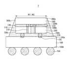
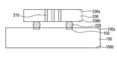
도 1을 참고하면, 본 발명의 제1 실시예에 따른 반도체 장치(1)는 실장 기판(100), 하부 반도체 칩(200), 상부 반도체 칩(300), 제1 언더필재(120) 및 제2 언더필재(110) 등을 포함한다.Referring to FIG. 1, the
실장 기판(100)은 패키지용 기판일 수 있고, 예를 들어, 인쇄용 회로 기판(PCB) 또는 세라믹 기판 등일 수 있다. 실장 기판(100)은 서로 대응하는 실장 기판의 상면(100a) 및 실장 기판의 하면(100b)을 포함한다. 실장 기판의 하면(100b)에는 반도체 장치(1)를 외부 장치에 전기적으로 연결하는 외부 단자(104)가 형성되어 있을 수 있다. 본딩 패드(102)는 외부 장치와 연결되는 외부 단자와 전기적으로 연결될 수 있고, 하부 반도체 칩(200) 및 상부 반도체 칩(300)에 전기적 신호를 공급할 수 있다. 또는, 본딩 패드(102) 중 적어도 하나는 예를 들어, 그라운드 패드일 수 있고, 실장 기판(100) 내의 접지라인과 전기적으로 연결될 수도 있다. 본딩 패드(102)는 실장 기판(100)의 예를 들어, 중앙부에 배치되는 것으로 도시되었으나, 이에 제한되는 것은 아니다.The mounting
하부 반도체 칩(200) 및 상부 반도체 칩(300)은 실장 기판(100) 상에 배치된다. 예를 들어, 하부 반도체 칩(200) 및 상부 반도체 칩(300)은 실장 기판(100) 상에 중첩되어 배치될 수 있고, 실장 기판(100) 상에 순차적으로 적층될 수 있다.The
제1 언더필재(120)는 하부 반도체 칩(200) 상에 배치된다. 제1 언더필재(120)는 하부 반도체 칩(200)과 상부 반도체 칩(300) 사이에 개재된다. 제1 언더필재(120)는 하부 반도체 칩(200)과 상부 반도체 칩(300)을 연결하여 본딩시킨다. 실장 기판(100) 상에 하부 반도체 칩(200)과, 제1 언더필재(120)와 상부 반도체 칩(300)이 순차적으로 적층되어 있다.The
하부 반도체 칩(200) 및 상부 반도체 칩(300)은 예를 들어, 메모리 칩, 로직 칩 등일 수 있다. 하부 반도체 칩(200) 및/또는 상부 반도체 칩(300)이 로직 칩일 경우, 하부 반도체 칩(200) 및/또는 상부 반도체 칩(300)은 수행하는 연산 등을 고려하여, 다양하게 설계될 수 있다. 하부 반도체 칩(200) 및/또는 상부 반도체 칩(300)이 메모리 칩일 경우, 메모리 칩은 예를 들어, 비휘발성 메모리 칩(non-volatile memory chip)일 수 있다. 구체적으로, 메모리 칩은 플래시 메모리 칩(flash memory chip)일 수 있다. 더욱 구체적으로, 메모리 칩은 낸드(NAND) 플래시 메모리 칩 또는 노어(NOR) 플래시 메모리 칩 중 어느 하나일 수 있다. 한편, 본 발명의 기술적 사상에 따른 메모리 장치의 형태가 이에 제한되는 것은 아니다. 본 발명의 몇몇 실시예에서, 메모리 칩은 PRAM(Phase-change Random-Access Memory), MRAM(Magneto-resistive Random-Access Memory), RRAM(Resistive Random-Access Memory) 중 어느 하나를 포함할 수도 있다.The
하부 반도체 칩(200)은 하부 반도체 칩의 하면(200b)에 형성되는 제1 연결 단자(220)에 의해 실장 기판(100)과 전기적으로 연결될 수 있다. 즉, 제1 연결 단자(220)는 하부 반도체 칩(200)과 실장 기판(100)의 본딩 패드(102)를 전기적으로 연결한다. 제1 연결 단자(220)는 볼 형태의 솔더 볼로 도시하였지만, 이에 제한되는 것은 아니다. 제1 연결 단자(220)는 필라(pillar)와 솔더 볼이 결합된 솔더 범프 타입일 수 있음은 물론이다.The
실장 기판(100)과 하부 반도체 칩(200) 사이에, 실장 기판(100)과 하부 반도체 칩(200)을 본딩하는 제1 연결 단자(220)가 위치하므로, 하부 반도체 칩(200)은 실장 기판(100)과 이격되어 배치되어 있다. 즉, 실장 기판의 상면(100a)과 하부 반도체 칩의 하면(200b)은 적어도 제1 연결 단자(220)의 높이만큼의 이격될 수 있다.Since the
하부 반도체 칩(200)은 하부 반도체 칩(200)을 관통하는 관통 전극(210)을 포함하다. 도 1에서, 하부 반도체 칩(200) 내에 관통 전극(210)은 3개 형성된 것으로 도시하였지만, 설명의 편이를 위한 것을 뿐, 이에 제한되는 것은 아니다.The
하부 반도체 칩(200)은 예를 들어, 플립칩(flip chip)의 형태를 할 수 있고, 제1 연결 단자(220)는 반도체 소자 회로가 형성된 면에 형성될 수 있으나, 이에 제한되는 것은 아니다.The
본 발명의 실시예들에 따른 반도체 장치에서, 관통 전극(210)을 포함하는 하부 반도체 칩(200)은 단일 칩인 것으로 도시하였지만, 이는 설명의 편이를 위한 것일 뿐, 이에 제한되는 것은 아니다.In the semiconductor device according to the embodiments of the present invention, although the
제1 언더필재(120)는 하부 반도체 칩의 상면(200a) 상에 배치된다. 제1 언더필재(120)는 필름 타입일 수 있다. 제1 언더필재(120)는 하부 반도체 칩의 상면(200a)과 상부 반도체 칩의 하면(300b)을 본딩시킨다.The
제1 언더필재(120)는 전기가 통하지 않는 비전도성 물질을 포함한다. 제1 언더필재(120)는 예를 들어, NCF(non-conductive film) 또는 DAF(die attach film) 등일 수 있지만, 이에 제한되는 것은 아니다.The
상부 반도체 칩(300)은 제1 언더필재(120) 상에 배치된다. 상부 반도체 칩(300)은 제1 언더필재(120)에 의해 하부 반도체 칩(200)에 본딩될 수 있다. 예를 들어, 제1 언더필재(120)는 상부 반도체 칩(300)이 실장 기판(100)과 본딩된 하부 반도체 칩(200)으로부터 분리되지 않도록 잡아주는 역할을 할 수 있다.The
상부 반도체 칩의 하면(300b)에 형성된 제2 연결 단자(310)는 하부 반도체 칩(200)과 연결됨으로써, 상부 반도체 칩(300)은 하부 반도체 칩(200)과 연결될 수 있다. 구체적으로, 제2 연결 단자(310)는 상부 반도체 칩(300)과 하부 반도체 칩(200) 내에 형성된 관통 전극(210)을 연결할 수 있다. 예를 들어, 상부 반도체 칩(300)은 하부 반도체 칩(200)과 전기적으로 연결될 수 있다. 상부 반도체 칩(300)은 예를 들어, 플립칩의 형태를 할 수 있고, 제2 연결 단자(310)는 반도체 소자 회로가 형성된 상부 반도체 칩(300)의 면 상에 형성될 수 있다. 제2 연결 단자(310)는 볼 형태의 솔더 볼로 도시하였지만, 이에 제한되는 것은 아니고, 필라(pillar)와 솔더 볼이 결합된 솔더 범프 형태일 수 있다. 구체적으로, 제2 연결 단자(310)는 마이크로 범프(micro bump)일 수 있다.The
또한, 상부 반도체 칩(300)은 하부 반도체 칩(200) 내에 형성된 관통 전극(210)을 매개로 실장 기판(100)과 전기적으로 연결될 수 있다. 구체적으로, 상부 반도체 칩(300)은 제2 연결 단자(310), 관통 전극(210) 및 제2 연결 단자(220)를 통해 실장 기판(100)과 전기적으로 연결될 수 있다.In addition, the
상부 반도체 칩(300)과 하부 반도체 칩(200)을 연결하는 제2 연결 단자(310)는 제1 언더필재(120)를 관통한다. 즉, 제1 언더필재(120)는 제2 연결 단자(310)의 둘레를 감싸고 있다.The
본 발명의 실시예들에 따른 반도체 장치에서, 하부 반도체 칩(200)과 전기적으로 연결되는 상부 반도체 칩(300)은 단일 칩인 것으로 도시하였지만, 이는 설명의 편이를 위한 것일 뿐, 이에 제한되는 것은 아니다.In the semiconductor device according to the embodiments of the present invention, although the
제2 언더필재(110)는 실장 기판(100) 상에 형성되고, 실장 기판(100)과 하부 반도체 칩(200) 사이의 공간을 채운다. 제2 언더필재(110)는 하부 반도체 칩(200)과 실장 기판(100) 사이에 위치하는 제1 연결 단자(220)를 전체적으로 감싼다. 또한, 제2 언더필재(110)는 하부 반도체 칩(200) 및 제1 언더필재(120)를 전체적으로 덮는다.The
제2 언더필재(110)는 하부 반도체 칩의 측면(200s)과 제1 언더필재의 측면(120s)를 전체적으로 감싼다. 또한, 제2 언더필재(110)는 상부 반도체 칩의 측면(300s)의 적어도 일부를 감싼다. 도 1에서는, 제2 언더필재(110)가 상부 반도체 칩의 측면(300s)을 전체적으로 감싸는 것으로 도시하였지만, 설명의 편의성을 위한 것일 뿐, 이에 제한되는 것은 아니다.The
제2 언더필재(110)는 상부 반도체 칩의 상면(300a) 상에는 배치되지 않는다. 즉, 상부 반도체 칩의 상면(300a)은 제2 언더필재(110)에 의해 노출된다.The
본 발명의 실시예들에 따른 반도체 장치에서, 제2 언더필재(110)는 실장 기판(100)과 하부 반도체 칩(200) 사이의 공간을 채울 뿐만 아니라, 하부 반도체 칩의 측면(200s) 및 상부 반도체 칩의 측면(300s)을 감싸므로, 실장 기판(100)과 하부 반도체 칩(200) 사이의 갭-필(gap-fill) 물질과 하부 반도체 칩의 측면(200s) 및 상부 반도체 칩의 측면(300s)을 감싸는 물질은 동일 레벨에서 형성되는 동일한 물질이다. 여기서, "동일 레벨"이라 함은 동일한 제조 공정에 의해 형성되는 것을 의미하는 것이다.In the semiconductor device according to embodiments of the present invention, the
하부 반도체 칩(200)과 상부 반도체 칩(300)은 필름 타입의 제1 언더필재(120)에 의해 본딩되므로, 제2 언더필재(110)는 하부 반도체 칩의 상면(200a)과 상부 반도체 칩의 하면(300b) 사이에 개재되지 않는다.Since the
제2 언더필재(110)는 경사를 갖는 외측면(110s)를 포함한다. 즉, 하부 반도체 칩(200) 및 상부 반도체 칩(300)과 인접하지 않고 외부로 노출되는 제2 언더필재의 외측면(110s)은 경사를 갖는다. 제2 언더필재의 외측면(110s)이 경사를 갖는 것은 제2 언더필재(110)가 모세관 언더필(capillary underfill, CUF)이기 때문이다.The
제2 언더필재(110)는 필름 타입의 제1 언더필재(120)와 다른 물질을 포함한다. 제2 언더필재(110)는 필름 타입이 아닌 페이스트(paste) 타입의 언더필(underfill) 물질을 포함할 수 있다. 제2 언더필재(110)는 예를 들어, 에폭시 수지 또는 이종 이상의 실리콘 하이브리드(silicone hybrid) 물질을 포함할 수 있다.The
도 1을 참고하면, 하부 반도체 칩(200)의 폭은 제1 폭(W1)이고, 상부 반도체 칩(300)의 폭은 제2 폭(W2)이다.Referring to FIG. 1, the width of the
본 발명의 제1 실시예에 따른 반도체 장치에서, 하부 반도체 칩(200)의 폭(W1)은 상부 반도체 칩(300)의 폭(W2)보다 크다. 따라서, 하부 반도체 칩(200)과 상부 반도체 칩(300) 사이에 개재되는 제1 언더필재(120)의 일부는 상부 반도체 칩(300)의 측면을 기준으로 돌출될 수 있다. 또한, 제1 언더필재(120)의 일부는 상부 반도체 칩의 측면(300s)의 일부를 감쌀 수 있다.In the semiconductor device according to the first embodiment of the present invention, the width W1 of the
이하에서, 도 2를 참고하여, 하부 반도체 칩(200)과 상부 반도체 칩(300)을 본딩하는 필름 타입의 제1 언더필재(120)의 형상에 대해서 설명한다. 좀 더 구체적으로, 제1 언더필재의 측면(120s) 형상에 대해서 설명한다.Hereinafter, the shape of the
제1 언더필재(120)는 필름 타입(film type)이므로, 제1 언더필재(120)는 유동성이 실질적으로 없다. 하지만, 제1 언더필재(120)를 경화시키는 제조 공정 전에 제1 언더필재(120)는 약간의 유동성을 가지고 있으므로, 제1 언더필재(120)에 압력이 가해질 경우, 제1 언더필재(120)는 측면으로 늘어남으로써, 측면으로 퍼질 수 있다. 즉, 제1 언더필재(120)에 압력이 가해진 상태로 제1 언더필재(120)가 경화되면, 제1 언더필재(120)의 일부는 상부 반도체 칩의 측면(300s)으로부터 측방으로 돌출될 수 있다.Since the
제1 언더필재의 측면(120s)은 제1 포인트(P1)와 제2 포인트(P2)와 제3 포인트(P3)를 포함한다. 제1 포인트(P1)은 하부 반도체 칩의 상면(200a)에서 가까운 지점이고, 제2 포인트(P2)는 하부 반도체 칩의 상면(200a)에서 제1 포인트(P1)보다 더 먼 지점이다. 또한, 제3 포인트(P3)는 하부 반도체 칩의 상면(200a)에서 제2 포인트(P2)보다 더 먼 지점이다. 즉, 제1 내지 제3 포인트(P1, P2, P3)는 하부 반도체 칩의 상면(200a)으로부터 점점 멀어지는 지점이다.The
이 때, 상부 반도체 칩의 측면(300s)의 연장선(EL)으로부터 제1 내지 제3 포인트(P1, P2, P3)까지의 거리는 각각 제1 거리(L1), 제2 거리(L2) 및 제3 거리(L3)일 수 있다.At this time, the distances from the extension lines EL of the side surfaces 300s of the upper semiconductor chip to the first to third points P1, P2, and P3 are the first distance L1, the second distance L2, and the third, respectively. It may be a distance L3.
본 발명의 실시예들에 따른 반도체 장치에서, 상부 반도체 칩의 측면(300s)의 연장선(EL)으로부터 제2 포인트(P2)까지의 거리(L2)는 상부 반도체 칩의 측면(300s)의 연장선(EL)으로부터 제1 포인트(P1)까지의 거리(L1)보다 크다. 또한, 상부 반도체 칩의 측면(300s)의 연장선(EL)으로부터 제2 포인트(P2)까지의 거리(L2)는 상부 반도체 칩의 측면(300s)의 연장선(EL)으로부터 제3 포인트(P3)까지의 거리(L1)보다 크다.In the semiconductor device according to embodiments of the present invention, the distance L2 from the extension line EL of the
다시 말하면, 제1 언더필재의 측면(120s) 중 가운데 부분에 위치하는 제2 포인트(P2)가 상부 반도체 칩의 측면(300s)의 연장선(EL)으로부터 가장 멀리 떨어져 있다.In other words, the second point P2 located at the center of the side surfaces 120s of the first underfill material is the farthest from the extension line EL of the side surfaces 300s of the upper semiconductor chip.
따라서, 제1 언더필재(120)는 두께 방향으로 중앙 부근의 폭이 가장 크고, 상부 반도체 칩(300) 및/또는 하부 반도체 칩(200)과 접하는 부근의 폭이 가장 작다.Therefore, the
제1 언더필재(120)의 이와 같은 형상은 상부 반도체 칩(300) 및 하부 반도체 칩(200)과 접하는 부분보다 상부 반도체 칩(300) 및 하부 반도체 칩(200)에서 이격된 부분이 좀 더 쉽게 늘어날 수 있기 때문이다.This shape of the
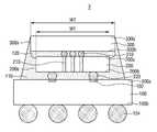
도 3을 참조하여, 본 발명의 제2 실시예에 따른 반도체 장치에 대해 설명한다. 설명의 편의를 위해, 전술한 제1 실시예와 다른 점을 중심으로 설명한다.A semiconductor device according to a second embodiment of the present invention will be described with reference to FIG. 3. For convenience of description, description will be made focusing on differences from the first embodiment described above.
도 3은 본 발명의 제2 실시예에 따른 반도체 장치를 설명하기 위한 도면이다.3 is a diagram for describing a semiconductor device according to a second embodiment of the present invention.
도 3을 참고하면, 하부 반도체 칩(200)의 폭(W1)은 상부 반도체 칩(300)의 폭(W2)과 실질적으로 동일하다.Referring to FIG. 3, the width W1 of the
제조 공정 중, 하부 반도체 칩(200)과 상부 반도체 칩(300)을 본딩시키기 위해, 압력을 가할 경우, 제1 언더필재(120)는 측면으로 늘어나, 하부 반도체 칩의 측면(200s) 및 상부 반도체 칩의 측면(300s)으로부터 돌출될 수 있다.During the manufacturing process, in order to bond the
도 2에서 설명했던 것과 같이, 본 발명의 제2 실시예에 따른 반도체 장치에서, 제1 언더필재(120)는 두께 방향으로 중앙 부근의 폭이 가장 크고, 상부 반도체 칩(300) 및/또는 하부 반도체 칩(200)과 접하는 부근의 폭이 가장 작다.As described in FIG. 2, in the semiconductor device according to the second embodiment of the present invention, the
도 3에서는, 제1 언더필재(120)는 하부 반도체 칩의 측면(200s) 및 상부 반도체 칩의 측면(300s)으로부터 돌출되었을 뿐, 하부 반도체 칩(200) 및 상부 반도체 칩(300)의 측면을 감싸지 않는 것으로 도시하였지만, 이에 제한되는 것은 아니다. 즉, 제1 언더필재(120)는 상부 반도체 칩의 측면(300s)의 일부 및/또는 하부 반도체 칩의 측면(200s)의 일부를 감쌀 수 있다.In FIG. 3, the
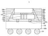
도 4를 참조하여, 본 발명의 제3 실시예에 따른 반도체 장치에 대해 설명한다. 설명의 편의를 위해, 전술한 제1 실시예와 다른 점을 중심으로 설명한다.A semiconductor device according to a third embodiment of the present invention will be described with reference to FIG. 4. For convenience of description, description will be made focusing on differences from the first embodiment described above.
도 4는 본 발명의 제3 실시예에 따른 반도체 장치를 설명하기 위한 도면이다.4 is a diagram for describing a semiconductor device according to a third embodiment of the present invention.
도 4를 참고하면, 하부 반도체 칩(200)의 폭(W1)은 상부 반도체 칩(300)의 폭(W2)보다 작다.Referring to FIG. 4, the width W1 of the
하부 반도체 칩(200)과 상부 반도체 칩(300) 사이에 개재되는 제1 언더필재(120)의 일부는 상부 반도체 칩(300)의 측면을 기준으로 돌출될 수 있다. 또한, 하부 반도체 칩(200)의 폭(W1)은 상부 반도체 칩(300)의 폭(W2)보다 작으므로, 제1 언더필재(120)는 하부 반도체 칩의 측면(200s)의 일부를 감쌀 수 있다.A portion of the
도 2에서 설명했던 것과 같이, 본 발명의 제3 실시예에 따른 반도체 장치에서, 제1 언더필재(120)는 두께 방향으로 중앙 부근의 폭이 가장 크고, 하부 반도체 칩(200)과 접하는 부근의 폭이 가장 작다.As described in FIG. 2, in the semiconductor device according to the third embodiment of the present invention, the
도 2를 통해 설명한 본 발명의 제1 실시예에 따른 반도체 장치에서, 제1 언더필재(120)는 상부 반도체 칩(300) 및/또는 하부 반도체 칩(200)과 접하는 부근의 폭이 가장 작다. 하지만, 도 4를 통해 설명하는 본 발명의 제3 실시예에 따른 반도체 장치에서, 제1 언더필재(120)는 하부 반도체 칩(200)과 접하는 부분의 폭이 가장 작다. 이와 같은 차이는 필름 타입의 제1 언더필재(120)는 제조 공정 중, 상부 반도체 칩의 하면(300b)에 부착된 상태로 제공되기 때문이다.In the semiconductor device according to the first embodiment of the present invention described with reference to FIG. 2, the
도 5를 참조하여, 본 발명의 제4 실시예에 따른 반도체 장치에 대해 설명한다. 설명의 편의를 위해, 전술한 제1 실시예와 다른 점을 중심으로 설명한다.A semiconductor device according to a fourth embodiment of the present invention will be described with reference to FIG. 5. For convenience of description, description will be made focusing on differences from the first embodiment described above.
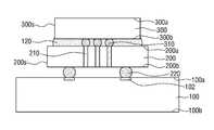
도 5는 본 발명의 제4 실시예에 따른 반도체 장치를 설명하기 위한 도면이다.5 is a diagram for describing a semiconductor device according to a fourth embodiment of the present invention.
도 5를 참고하면, 본 발명의 제4 실시예에 따른 반도체 장치(4)는 히트 싱크(400)를 더 포함한다.Referring to FIG. 5, the semiconductor device 4 according to the fourth embodiment of the present invention further includes a
히트 싱크(400)는 상부 반도체 칩(300) 상에 배치된다. 즉, 실장 기판(100) 상에 하부 반도체 칩(200), 상부 반도체 칩(300) 및 히트 싱크(400)가 순차적으로 적층된다. 히트 싱크(400)는 예를 들어, 평평한 판재 또는 얇은 포일(foil) 형태일 수 있다.The
히트 싱크(400)는 열전도성(heat conductivity)이 큰 물질을 포함할 수 있다. 히트 싱크(400)는 예를 들어, 금속 판재 또는 금속 포일 일 수 있고, 구체적으로 예를 들어, 구리 판재, 알루미늄 판재, 구리 포일, 알루미늄 포일 또는 이들의 조합일 수 있으나, 이에 제한되는 것은 아니다.The
열전달 물질층(410)은 히트 싱크(400)과 상부 반도체 칩(300) 사이에 개재될 수 있다. 즉, 열전달 물질층(410)은 상부 반도체 칩의 상면(300a)과 히트 싱크(400) 사이에 배치될 수 있다. 열전달 물질층(410)은 상부 반도체 칩의 상면(300a) 상에 직접 접하여 형성될 수 있다. 열전달 물질층(410)은 히트 싱크(400)와 상부 반도체 칩(300)을 연결시킨다. 열전달 물질층(410)은 상부 반도체 칩(300) 및 하부 반도체 칩(200) 등에서 발생되는 열을 히트 싱크(400)로 전달시킨다.The heat
열전달 물질층(410)은 열 전달 물질(TIM: Thermal Interface Material)을 포함하고, 접착 특성을 갖는다. 열전달 물질층(410)은 예를 들어, 에폭시 레진(epoxy resin)에 은(Ag)과 같은 금속 또는 알루미나(Al2O3)와 같은 금속 산화물 계열의 입자를 포함한 경화성 접착물질이거나, 다이아몬드, 질화 알루미늄(AlN), 알루미나(Al2O3), 산화 아연(ZnO), 은(Ag) 등의 입자를 포함한 써멀 그리스(thermal grease)일 수 있지만, 이에 제한되는 것은 아니다.The heat
도 5에서, 히트 싱크(400)의 폭은 상부 반도체 칩(300)의 폭과 실질적으로 동일한 것으로 도시하였지만, 설명의 편이를 위한 것을 뿐, 이에 제한되는 것은 아니다.In FIG. 5, the width of the
즉, 히트 싱크(400)는 열전달 물질층(410)을 매개로 상부 반도체 칩(300)과 연결되면 되므로, 히트 싱크(400)의 폭은 상부 반도체 칩(300)의 폭보다 클 수도 있고, 작을 수도 있음은 물론이다.That is, since the
도 6을 참조하여, 본 발명의 제5 실시예에 따른 반도체 장치에 대해 설명한다. 설명의 편의를 위해, 전술한 제1 실시예와 다른 점을 중심으로 설명한다.The semiconductor device according to the fifth embodiment of the present invention will be described with reference to FIG. 6. For convenience of description, description will be made focusing on differences from the first embodiment described above.
도 6은 본 발명의 제5 실시예에 따른 반도체 장치를 설명하기 위한 도면이다.6 is a view for explaining a semiconductor device according to a fifth embodiment of the present invention.
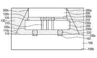
도 6을 참고하면, 본 발명의 제5 실시예에 따른 반도체 장치(5)는 패키지 몰딩재(130)를 더 포함한다.Referring to FIG. 6, the semiconductor device 5 according to the fifth embodiment of the present invention further includes a
패키지 몰딩재(130)는 실장 기판(100) 상에 형성된다. 패키지 몰딩재(130)는 제2 언더필재(110)를 덮는다. 패키지 몰딩재(130)는 상부 반도체 칩의 상면(300a)을 노출시킨다. 패키지 몰딩재(130)의 상면과 상부 반도체 칩의 상면(300a)은 동일 평면 상에 놓일 수 있다.The
패키지 몰딩재(130)는 예를 들어, 에폭시 몰딩 컴파운드(EMC, Epoxy Molding Compound) 또는 이종 이상의 실리콘 하이브리드 물질을 포함할 수 있다.The
도 6에서, 패키지 몰딩재(130)는 제2 언더필재(110)의 측면에 접하고, 상부 반도체 칩의 측면(300s)과 접하지 않는 것으로 도시되었지만, 이에 제한되는 것은 아니다.In FIG. 6, the
즉, 제2 언더필재(110)가 상부 반도체 칩의 측면(300s)의 일부를 감싸서, 상부 반도체 칩의 측면(300s)의 나머지가 제2 언더필재(110)에 의해 노출될 경우, 패키지 몰딩재(130)는 상부 반도체 칩의 측면(300s)의 나머지를 접하여 감쌀 수 있음은 물론이다.That is, when the
도 7을 참조하여, 본 발명의 제6 실시예에 따른 반도체 장치에 대해 설명한다. 설명의 편의를 위해, 전술한 제5 실시예와 다른 점을 중심으로 설명한다.A semiconductor device according to a sixth embodiment of the present invention will be described with reference to FIG. 7. For convenience of description, description will be made focusing on differences from the above-described fifth embodiment.
도 7은 본 발명의 제6 실시예에 따른 반도체 장치를 설명하기 위한 도면이다.7 is a diagram for describing a semiconductor device according to a sixth embodiment of the present invention.
도 7을 참고하면, 본 발명의 제6 실시예에 따른 반도체 장치(6)는 히트 싱크(400)를 더 포함한다.Referring to FIG. 7, the
열전달 물질층(410)은 상부 반도체 칩의 상면(300a) 및 패키지 몰딩재(130)의 상면 상에 형성된다. 열전달 물질층(410)은 상부 반도체 칩의 상면(300a) 및 패키지 몰딩재(130)의 상면에 직접 접하여 형성될 수 있다.The heat
히트 싱크(400)는 열전달 물질층(410) 상에 형성된다. 다시 말하면, 히트 싱크(400)는 상부 반도체 칩(300)과 패키지 몰딩재(130) 상에 형성되어, 상부 반도체 칩(300)과 패키지 몰딩재(130)와 오버랩된다.The
도 8 내지 도 14를 참조하여, 본 발명의 제1 실시예에 따른 반도체 장치 제조 방법에 대해서 설명한다. 본 발명의 제1 실시예에 따른 반도체 장치 제조 방법에 의해, 본 발명의 제1 내지 제3 실시예에 따른 반도체 장치가 제조될 수 있다.A method for manufacturing a semiconductor device according to a first embodiment of the present invention will be described with reference to FIGS. 8 to 14. By the semiconductor device manufacturing method according to the first embodiment of the present invention, the semiconductor devices according to the first to third embodiments of the present invention can be manufactured.
도 8 내지 도 14는 본 발명의 제1 실시예에 따른 반도체 장치 제조 방법을 설명하기 위한 중간단계 도면들이다.8 to 14 are intermediate stage views for explaining a method of manufacturing a semiconductor device according to a first embodiment of the present invention.
도 8을 참고하면, 제1 연결 단자(220)가 형성된 하부 반도체 칩(200)을 제공한다.Referring to FIG. 8, a
구체적으로, 복수의 하부 반도체 칩(200)이 배열된 제1 반도체 기판(205)이 제공된다. 제1 반도체 기판(205)은 각각 관통 전극(210)이 형성된 복수의 하부 반도체 칩(200)을 포함한다. 하부 반도체 칩(200)은 예를 들어, 메모리 소자 또는 로직 소자일 수 있다.Specifically, a
이어서, 하부 반도체 칩의 하면(200b) 상에 제1 연결 단자(220)를 형성한다. 제1 연결 단자(220)는 각각의 하부 반도체 칩(200)의 일면 상에 형성되어, 하부 반도체 칩(200)에 전기적인 신호를 입출력하는 입출력 단자일 수 있다.Subsequently, the
이어서, 도 8에는 도시되지 않았지만, 제1 연결 단자(220)가 형성된 제1 반도체 기판(205)을 캐리어에 부착시킬 수 있다.Subsequently, although not illustrated in FIG. 8, the
이어서, 다이싱 공정(10)을 통해, 제1 반도체 기판(205)을 자른다. 다이싱 공정(10)으로 잘려진 제1 반도체 기판(205)은 복수의 하부 반도체 칩(200)으로 분리된다.Subsequently, the
즉, 제1 연결 단자(220)가 하부 반도체 칩의 하면(200b)에 형성된 하부 반도체 칩(200)을 제공한다.That is, the
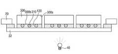
도 9 및 도 10을 참고하면, 상부 반도체 칩의 하면(300b)에 제2 연결 단자(310) 및 필름 타입의 제1 언더필재(120)가 형성된 상부 반도체 칩(300)을 제공한다.Referring to FIGS. 9 and 10, an
구체적으로, 복수의 상부 반도체 칩(300)이 배열된 제2 반도체 기판(305)이 제공된다. 상부 반도체 칩(300)은 예를 들어, 메모리 소자 또는 로직 소자일 수 있다.Specifically, a
이어서, 상부 반도체 칩의 하면(300b) 상에 제2 연결 단자(310)를 형성한다. 제2 연결 단자(310)는 각각의 상부 반도체 칩(300)의 일면 상 즉, 상부 반도체 칩의 하면(300b)에 형성되어, 상부 반도체 칩(300)에 전기적인 신호를 입출력하는 입출력 단자일 수 있다.Subsequently, the
이어서, 접착 테이프(30)를 이용하여, 제2 연결 단자(310)가 형성된 제2 반도체 기판(305)을 웨이퍼링(20)에 접착시킨다. 제2 연결 단자(310)가 형성된 상부 반도체 칩의 하면(300b)이 접착 테이프(30)와 마주보도록 제2 반도체 기판(305)을 웨이퍼링(20)에 접착시킨다.Subsequently, the
접착 테이프(30)는 하부 접착막(32)과 상부 접착막(34)을 포함한다. 하부 접착막(32)과 상부 접착막(34)은 층상 형태로 형성되어 있다. 접착 테이프에 포함되는 하부 접착막(32) 및 상부 접착막(34)은 이 후에 설명하는 공정을 통해서, 서로 분리될 수 있다. 상부 접착막(34)은 예를 들어, NCF(non-conductive film) 또는 DAF(die attach film) 등일 수 있지만, 이에 제한되는 것은 아니다. 하부 접착막(32)은 상부 접착막(34)과 붙을 수 있고, 이 후의 익스팬션(expansion) 공정에서 늘어날 수 있는 물질이면 된다.The
제2 연결 단자(310)가 형성된 제2 반도체 기판(305)은 구체적으로, 상부 접착막(34)에 접착될 수 있다. 또한, 제2 연결 단자(310)는 상부 접착막(34) 내로 만입되어 있다. 즉, 상부 반도체 칩의 하면(300b)은 상부 접착막(34)과 접하고, 제2 연결 단자(310)는 상부 접착막(34)에 의해 둘러싸여 있다.Specifically, the
이어서, 다이싱 공정(10)을 통해, 제2 반도체 기판(305)을 자른다. 다이싱 공정(10)으로 잘려진 제2 반도체 기판(305)은 복수의 상부 반도체 칩(300)으로 분리된다. 다이싱 공정(10)을 통해, 상부 접착막(34)의 적어도 일부는 분리되지만, 하부 접착막(32)은 분리되지 않는다.Subsequently, the
이어서, 익스팬션 공정을 통해, 분리된 상부 반도체 칩(300) 사이의 거리를 넓혀준다. 익스팬션 공정을 통해, 각각의 상부 반도체 칩의 하면(300b)에 접착된 상부 접착막(34)은 분리가 된다. 분리된 상부 접착막(34)은 필름 타입의 제1 언더필재(120)가 된다.Subsequently, a distance between the separated
이어서, 광학적 분리 공정(40)을 통해, 제1 언더필재(120)와 하부 접착막(32)을 분리한다. 광학적 분리 공정(40)은 예를 들어, 자외선 조사(UV irradiation) 방법 또는 레이저 조사(laser irradiation) 방법 등을 이용할 수 있다.Subsequently, the
이를 통해, 상부 반도체 칩의 하면(300b)에 제2 연결 단자(310)와 필름 타입의 제1 언더필재(120)가 형성된 상부 반도체 칩(300)이 제공된다. 상부 반도체 칩의 하면(300b) 상에 형성된 제1 언더필재(120)는 제2 연결 단자(310)와 상부 반도체 칩의 하면(300b)을 덮고 있다. 상부 반도체 칩(300)은 하부 반도체 칩(200)과 마찬가지로 서로 대향되는 상부 반도체 칩의 상면(300a)과 상부 반도체 칩의 하면(300b)을 포함한다.Through this, the
도 11을 참고하면, 하부 반도체 칩(200)을 실장 기판(100)에 본딩한다. 좀 더 구체적으로, 제1 연결 단자(220)가 형성된 하부 반도체 칩(200)을 실장 기판의 상면(100a)에 본딩한다.Referring to FIG. 11, the
하부 반도체 칩(200)은 하부 반도체 칩의 하면(200b)에 형성된 제1 연결 단자(220)를 이용하여, 실장 기판(100)에 본딩된다. 하부 반도체 칩(200) 및 실장 기판(100)이 본딩됨으로써, 하부 반도체 칩(200)과 실장 기판(100)은 전기적으로 연결된다. 예를 들어, 제1 연결 단자(220)는 실장 기판의 상면(100a)에 형성된 본딩 패드(102)와 접속할 수 있다.The
도 12를 참고하면, 제1 언더필재(120)를 이용하여, 하부 반도체 칩(200)과 상부 반도체 칩(300)을 본딩한다.Referring to FIG. 12, the
필름 타입의 제1 언더필재(120)는 상부 반도체 칩의 하면(300b)에 형성된 상태로 제공된다. 제1 언더필재(120)가 형성된 상부 반도체 칩(300)을 하부 반도체 칩(200) 상에 배치한다. 제1 언더필재(120)를 이용하여, 상부 반도체 칩의 하면(300b)과 하부 반도체 칩의 상면(200a)을 본딩한다.The film type
하부 반도체 칩(200)과 상부 반도체 칩(300)이 본딩될 때, 하부 반도체 칩(200)과 마주하는 상부 반도체 칩의 하면(300b)에 형성된 제2 연결 단자(310)는 하부 반도체 칩(200)과 연결된다. 구체적으로, 제2 연결 단자(310)는 하부 반도체 칩(200)에 형성된 관통 전극(210)과 연결된다. 이를 통해, 상부 반도체 칩(300)은 하부 반도체 칩(200)과 전기적으로 연결된다. 또한, 상부 반도체 칩(300)은 실장 기판(100)과도 전기적으로 연결된다.When the
하부 반도체 칩(200)과 상부 반도체 칩(300)이 본딩되기 전에, 제1 언더필재(120)는 제2 연결 단자(310)를 덮고 있었다. 따라서, 하부 반도체 칩(200)과 상부 반도체 칩(300)이 본딩된 후에는, 제1 언더필재(120)는 제2 연결 단자(310)를 감싼다.Before the
도 12에서 도시한 것과 같이, 하부 반도체 칩(200)의 폭이 상부 반도체 칩(300)의 폭보다 클 경우, 상부 반도체 칩(300)을 하부 반도체 칩(200)에 본딩할 때, 제1 언더필재(120)는 폭이 좁은 상부 반도체 칩의 측면(300s) 일부를 감쌀 수 있다.As illustrated in FIG. 12, when the width of the
만약, 도 3에서 설명한 것과 같이, 하부 반도체 칩(200)의 폭이 상부 반도체 칩(300)의 폭과 실질적으로 동일한 경우, 제1 언더필재(120)는 하부 반도체 칩(200) 및 상부 반도체 칩(300)의 측면을 감싸지 않을 수 있다. 또는, 제1 언더필재(120)는 상부 반도체 칩의 측면(300s)의 일부 및/또는 하부 반도체 칩의 측면(200s)의 일부를 감쌀 수 있다.If the width of the
덧붙여, 도 4에서 설명한 것과 같이, 하부 반도체 칩(200)의 폭이 상부 반도체 칩(300)의 폭보다 작을 경우, 제1 언더필재(120)는 하부 반도체 칩의 측면(200s)의 일부를 감쌀 수 있다.In addition, as described in FIG. 4, when the width of the
필름 타입의 제1 언더필재(120)에 의해 상부 반도체 칩(300)과 하부 반도체 칩(200)이 본딩되므로, 제1 언더필재(120)는 두께 방향으로 중앙 부근의 폭이 가장 크고, 상부 반도체 칩(300) 및/또는 하부 반도체 칩(200)과 접하는 부근의 폭이 가장 작을 수 있다.Since the
도 13을 참고하면, 플라즈마 공정(50)을 통해, 실장 기판(100)과 하부 반도체 칩(200)과 상부 반도체 칩(300)을 플라즈마 처리한다.Referring to FIG. 13, through the
실장 기판(100)과 하부 반도체 칩(200)과 상부 반도체 칩(300)을 플라즈마 처리함으로써, 플라즈마 공정(50)에 노출된 실장 기판(100)과 하부 반도체 칩(200)과 상부 반도체 칩(300)의 각각의 면들은 모세관 현상이 잘 발생할 수 있는 표면 상태로 바뀌게 된다.Plasma processing the mounting
플라즈마 공정(50)을 통해, 하부 반도체 칩의 하면(200b)과 하부 반도체 칩의 하면(200b)과 마주보는 실장 기판의 상면(100a)도 플라즈마 처리됨은 물론이다.It goes without saying that through the
도 14를 참고하면, 실장 기판(100)과 하부 반도체 칩(200) 사이의 공간을 채우는 제2 언더필재(110)를 형성한다. 또한, 제2 언더필재(110)는 하부 반도체 칩의 측면(200s) 및 상부 반도체 칩의 측면(300s)의 적어도 일부를 감싼다.Referring to FIG. 14, a
하부 반도체 칩의 하면(200b)과 실장 기판의 상면(100a) 사이의 공간을 채우는 제2 언더필재(110)는 제1 연결 단자(220)를 전체적으로 감싼다.The
제2 언더필재(110)를 형성하는 것은 예를 들어, 모세관 언더필(capillary underfill) 방법 등을 이용할 수 있다. 좀 더 구체적으로, 제2 언더필재(110)를 형성하는 물질을 실장 기판의 상면(100a)에 디스펜싱(dispending)한다. 디스펜싱된 제2 언더필재(110)를 형성하는 물질은 하부 반도체 칩의 하면(200b)과 실장 기판의 상면(100a) 사이로 흐르게 된다. 또한, 디스펜싱된 제2 언더필재(110)를 형성하는 물질은 하부 반도체 칩의 측면(200s) 및 상부 반도체 칩의 측면(300s)을 따라서도 움직이게 된다.To form the
이와 같이, 디스펜싱된 제2 언더필재(110)를 형성하는 물질이 하부 반도체 칩의 하면(200b)과 실장 기판의 상면(100a) 사이 공간과 하부 반도체 칩의 측면(200s) 및 상부 반도체 칩의 측면(300s)을 따라 움직이는 것은 플라즈마 공정(50)을 통해, 표면을 플라즈마 처리했기 때문이다.In this way, the material forming the dispensed
모세관 언더필 방법을 이용하여 제2 언더필재(110)를 형성하지만, 하부 반도체 칩(200)과 상부 반도체 칩(300) 사이에는 제2 언더필재(110)가 형성되지 않는다. 즉, 필름 타입의 제1 언더필재(120)는 상부 반도체 칩의 하면(300b)을 전체적으로 덮은 상태로 제공되어 하부 반도체 칩(200)과 상부 반도체 칩(300)이 본딩된다. 따라서, 제2 언더필재(110)는 하부 반도체 칩(200)과 상부 반도체 칩(300) 사이에 개재되지 않는다. 다시 말하면, 하부 반도체 칩의 상면(200a)과 상부 반도체 칩의 하면(300b) 사이에는 제2 언더필재(110)가 존재하지 않는다.The
플라즈마 공정(50)을 통해, 상부 반도체 칩의 상면(300a)은 플라즈마 처리가 되었지만, 제2 언더필재(110)는 상부 반도체 칩의 상면(300a) 상에 형성되지 않을 수 있다. 즉, 제2 언더필재(110)에 의해, 상부 반도체 칩의 상면(300a)은 노출된다.Through the
제2 언더필재(110)는 모세관 언더필 방법에 의해서 형성되므로, 제2 언더필재의 외측면(110s)는 경사를 갖도록 형성될 수 있다.Since the
도 14에서, 제2 언더필재(110)는 상부 반도체 칩의 측면(300s)을 전체적으로 감싸는 것으로 도시하였지만, 이에 제한되는 것은 아니다.In FIG. 14, the
또한, 도 13에서 설명한 플라즈마 공정(50)에 의해 제1 언더필재(120)의 측면도 플라즈마 처리가 되므로, 제2 언더필재(110)는 상부 반도체 칩의 측면(300s)으로부터 돌출된 제1 언더필재(120)도 덮는다.In addition, since the side surface of the
도 1을 참고하며, 실장 기판의 하면(100b)에 외부 단자(104)를 형성한다.Referring to FIG. 1, an
도 8 내지 도 15를 참조하여, 본 발명의 제2 실시예에 따른 반도체 장치 제조 방법에 대해서 설명한다. 본 발명의 제2 실시예에 따른 반도체 장치 제조 방법에 의해, 본 발명의 제4 실시예에 따른 반도체 장치가 제조될 수 있다.A method for manufacturing a semiconductor device according to a second embodiment of the present invention will be described with reference to FIGS. 8 to 15. By the semiconductor device manufacturing method according to the second embodiment of the present invention, the semiconductor device according to the fourth embodiment of the present invention can be manufactured.
도 15는 본 발명의 제2 실시예에 따른 반도체 장치 제조 방법을 설명하기 위한 중간단계 도면이다.15 is an intermediate step diagram for describing a method of manufacturing a semiconductor device according to a second embodiment of the present invention.
도 15를 참고하면, 상부 반도체 칩(300) 상에 히트 싱크(400)를 형성한다.Referring to FIG. 15, a
적층된 하부 반도체 칩(200)과, 상부 반도체 칩(300) 등에서 발생하는 열을 좀 더 빠르고 효율적으로 제거하기 위해, 제2 언더필재(110)를 형성한 후, 상부 반도체 칩의 상면(300a) 상에 히트 싱크(400)를 더 형성할 수 있다.In order to more quickly and efficiently remove the heat generated from the stacked
제2 언더필재(110)에 의해 노출되는 상부 반도체 칩의 상면(300a)에 열전달 물질층(410)을 형성한다.The heat
이어서, 열전달 물질층(410) 상에 히트 싱크(400)를 배치한다. 열전달 물질층(410)은 히트 싱크(400)과 상부 반도체 칩(300) 사이의 접착제 역할을 한다.Next, the
도 8 내지 도 16을 참조하여, 본 발명의 제3 실시예에 따른 반도체 장치 제조 방법에 대해서 설명한다. 본 발명의 제3 실시예에 따른 반도체 장치 제조 방법에 의해, 본 발명의 제5 실시예에 따른 반도체 장치가 제조될 수 있다.A method for manufacturing a semiconductor device according to a third embodiment of the present invention will be described with reference to FIGS. 8 to 16. By the semiconductor device manufacturing method according to the third embodiment of the present invention, the semiconductor device according to the fifth embodiment of the present invention can be manufactured.
도 16은 본 발명의 제3 실시예에 따른 반도체 장치 제조 방법을 설명하기 위한 중간단계 도면이다.16 is an intermediate step diagram for describing a semiconductor device manufacturing method according to a third embodiment of the present invention.
도 16을 참고하면, 실장 기판(100) 상에, 제2 언더필재(110)를 덮는 패키지 몰딩재(130)를 형성한다.Referring to FIG. 16, a
패키지 몰딩재(130)는 상부 반도체 칩의 상면(300a) 상에는 형성되지 않는다. 즉, 상부 반도체 칩의 상면(300a)은 패키지 몰딩재(130)에 의해 노출된다. 패키지 몰딩재(130)의 상면과 상부 반도체 칩의 상면(300a)은 동일 평면 상에 놓일 수 있다.The
패키지 몰딩재(130)는 몰드를 이용하여 형성한다. 따라서, 패키지 몰딩재(130)가 상부 반도체 칩의 상면(300a) 상에도 형성될 수 있다. 이와 같은 경우, 상부 반도체 칩의 상면(300a) 상에 형성된 패키지 몰딩재(130)를 평탄화 공정 등으로 제거하여, 상부 반도체 칩의 상면(300a)을 노출시킨다.The
도 17은 본 발명의 실시예들에 따른 반도체 장치를 포함하는 메모리 카드의 블록도이다.17 is a block diagram of a memory card including a semiconductor device according to embodiments of the present invention.
도 17을 참조하면, 본 발명의 다양한 실시예들에 따른 반도체 장치를 포함하는 메모리(1210)는 메모리 카드(1200)에 채용될 수 있다. 메모리 카드(1200)는 호스트(1230)와 메모리(1210) 사이에서 데이터 교환을 컨트롤하는 메모리 컨트롤러(1220)를 포함할 수 있다. SRAM(1221)은 중앙 처리 장치(1222)의 동작 메모리로 사용될 수 있다. 호스트 인터페이스(1223)은 호스트(1230)가 메모리 카드(1200)에 접속하여 데이터를 교환하기 위한 프로토콜을 포함할 수 있다. 에러 정정 코드(1224)는 메모리(1210)로부터 리드된 데이터의 에러를 탐지하고 정정할 수 있다. 메모리 인터페이스(1225)는 메모리(1210)와 인터페이싱할 수 있다. 중앙 처리 장치(1222)는 메모리 컨트롤러(1220)의 데이터 교환과 관련된 전체적인 컨트롤 동작을 수행할 수 있다.Referring to FIG. 17, a
도 18은 본 발명의 실시예들에 따른 반도체 장치를 이용한 정보 처리 시스템의 블록도이다.18 is a block diagram of an information processing system using a semiconductor device according to embodiments of the present invention.
도 18을 참조하면, 정보 처리 시스템(1300)은 본 발명의 다양한 실시예들에 따른 반도체 장치를 포함하는 메모리 시스템(1310)을 포함할 수 있다. 정보 처리 시스템(1300)은, 시스템 버스(1360)와 전기적으로 접속된, 메모리 시스템(1310), 모뎀(1320), 중앙 처리 장치(1330), RAM(1340) 및 사용자 인터페이스(1350)를 포함할 수 있다. 메모리 시스템(1310)은 메모리(1311)와, 메모리 컨트롤러(1312)를 포함할 수 있으며, 도 9에 도시된 메모리 카드(1200)와 실질적으로 동일한 구성을 가질 수 있다. 중앙 처리 장치(1330)에 의해 처리되는 데이터 또는 외부 장치로부터 수신되는 데이터는 메모리 시스템(1310)에 저장될 수 있다. 정보 처리 시스템(1300)은 메모리 카드, SSD, 카메라 이미지 센서 및 기타 다양한 칩셋에 적용될 수 있다. 예를 들어, 메모리 시스템(1310)은 SSD가 채용되도록 구성될 수 있으며, 이 경우, 정보 처리 시스템(1300)은 대용량의 데이터를 안정적이고 신뢰성있게 처리할 수 있다.Referring to FIG. 18, the
도 19는 본 발명의 본 발명의 실시예들에 따른 반도체 장치를 포함하는 전자 장치의 블록도이다.19 is a block diagram of an electronic device including a semiconductor device according to embodiments of the present invention.
도 19를 참조하면, 전자 장치(1400)은 본 발명의 다양한 실시예들에 따라 제조된 반도체 장치를 포함할 수 있다. 전자 장치(1400)는 무선 통신 기기(예를 들어, PDA, 노트북, 휴대용 컴퓨터, 웹 테블릿, 무선 전화기, 및/또는 무선 디지털 음악 재생기) 또는 무선 통신 환경에서 정보를 주고 받는 다양한 기기에 사용될 수 있다.Referring to FIG. 19, the
전자 장치(1400)는 컨트롤러(1410), 입/출력 장치(1420), 메모리(1430), 및 무선 인터페이스(1440)를 포함할 수 있다. 여기서, 메모리(1430)는 본 발명의 다양한 실시예들에 따라 제조된 반도체 장치를 포함할 수 있다. 컨트롤러(1410)는 마이크로프로세서, 디지털 시그널 프로세서, 또는 이와 유사한 프로세서를 포함할 수 있다. 메모리(1430)는 컨트롤러(1410)에 의해 처리되는 커맨드(또는 사용자 데이터)를 저장하는데 이용될 수 있다. 무선 인터페이스(1440)는 무선 데이터 네트워크를 통해 데이터를 주고 받는데 이용될 수 있다. 무선 인터페이스(1440)는 안테나 및/또는 무선 트랜시버(transceiver)를 포함할 수 있다. 전자 장치(1400)는 예를 들어, CDMA, GSM, NADC, E-TDMA, WCDMA, CDMA2000과 같은 제3 세대 통신 시스템 프로토콜을 이용할 수 있다.The
이상 첨부된 도면을 참조하여 본 발명의 실시예를 설명하였지만, 본 발명이 속하는 기술분야에서 통상의 지식을 가진 자는 본 발명이 그 기술적 사상이나 필수적인 특징을 변경하지 않고서 다른 구체적인 형태로 실시될 수 있다는 것을 이해할 수 있을 것이다. 그러므로 이상에서 기술한 실시예들은 모든 면에서 예시적인 것이며 한정적이 아닌 것으로 이해해야만 한다.Although the embodiments of the present invention have been described with reference to the accompanying drawings, those skilled in the art to which the present invention pertains may be implemented in other specific forms without changing the technical spirit or essential features of the present invention. You will understand. Therefore, it should be understood that the embodiments described above are illustrative in all respects and not restrictive.
100: 실장 기판110, 120: 언더필재
130: 패키지 몰딩재200: 하부 반도체 칩
210: 관통 전극220, 310: 연결 단자
300: 상부 반도체 칩400: 히트 싱크
100: mounting
130: package molding material 200: lower semiconductor chip
210: through
300: upper semiconductor chip 400: heat sink
Claims (10)
Translated fromKorean서로 대향되는 상면과 하면을 포함하고, 상기 하면에 제2 연결 단자와 필름 타입의 제1 언더필재가 형성된 제2 반도체 칩을 제공하고,
상기 제1 연결 단자를 이용하여, 상기 제1 반도체 칩을 실장 기판에 본딩하고,
상기 제1 언더필재에 압력을 가하여, 상기 제1 반도체 칩과 상기 제2 반도체 칩을 본딩하고,
상기 실장 기판과 상기 제1 반도체 칩 사이의 공간을 채우고, 상기 제2 반도체 칩의 측면의 적어도 일부와 상기 제1 반도체 칩의 측면의 적어도 일부를 감싸는 제2 언더필재를 형성하는 것을 포함하되,
상기 가압에 의해 상기 제1 언더필재는 상기 제1 반도체 칩 및 상기 제2 반도체 칩의 측면보다 돌출되는 반도체 장치 제조 방법.Providing a first semiconductor chip on which the first connection terminal is formed,
A second semiconductor chip including an upper surface and a lower surface facing each other, wherein a second connection terminal and a film type first underfill material are formed on the lower surface,
Bonding the first semiconductor chip to the mounting substrate using the first connection terminal,
Applying pressure to the first underfill material, bonding the first semiconductor chip and the second semiconductor chip,
Filling a space between the mounting substrate and the first semiconductor chip, and forming a second underfill material surrounding at least a portion of the side surface of the second semiconductor chip and at least a portion of the side surface of the first semiconductor chip,
A method of manufacturing a semiconductor device, wherein the first underfill material protrudes from side surfaces of the first semiconductor chip and the second semiconductor chip by the pressing.
상기 제1 반도체 칩과 상기 제2 반도체 칩을 본딩할 때, 상기 제1 언더필재는 상기 제2 반도체 칩의 측면의 일부를 감싸는 반도체 장치 제조 방법.According to claim 1,
When bonding the first semiconductor chip and the second semiconductor chip, the first underfill material surrounds a portion of the side surface of the second semiconductor chip.
상기 제1 반도체 칩과 상기 제2 반도체 칩을 본딩할 때, 상기 제1 언더필재는 상기 제1 반도체 칩의 측면의 일부를 감싸는 반도체 장치 제조 방법.According to claim 1,
When bonding the first semiconductor chip and the second semiconductor chip, the first underfill material surrounds a portion of the side surface of the first semiconductor chip.
상기 제2 언더필재를 형성하는 것은 상기 제2 반도체 칩의 상면을 노출시키는 것을 포함하는 반도체 장치 제조 방법.According to claim 1,
Forming the second underfill material comprises exposing an upper surface of the second semiconductor chip.
상기 제2 언더필재를 형성한 후, 상기 제2 반도체 칩의 상면 상에 히트 싱크(heat sink)를 형성하는 것을 더 포함하는 반도체 장치 제조 방법.The method of claim 4,
After forming the second underfill material, a method of manufacturing a semiconductor device further comprising forming a heat sink on a top surface of the second semiconductor chip.
상기 제2 언더필재는 모세관 언더필(capillary underfill) 방법을 이용하여 형성하는 것을 포함하는 반도체 장치 제조 방법.According to claim 1,
The second underfill material is a semiconductor device manufacturing method comprising forming using a capillary underfill method.
상기 제2 언더필재를 형성하기 전에,
상기 실장 기판과, 상기 제1 반도체 칩과, 상기 제2 반도체 칩을 플라즈마 처리하는 것을 더 포함하는 반도체 장치 제조 방법.The method of claim 6,
Before forming the second underfill material,
A method of manufacturing a semiconductor device further comprising plasma processing the mounting substrate, the first semiconductor chip, and the second semiconductor chip.
상기 실장 기판 상에, 상기 제2 언더필재를 덮고 상기 제2 반도체 칩의 상면을 노출시키는 몰딩재를 형성하는 것을 더 포함하는 반도체 장치 제조 방법.According to claim 1,
And forming a molding material covering the second underfill material and exposing an upper surface of the second semiconductor chip on the mounting substrate.
필름 타입의 제1 언더필재에 압력을 가하여, 실장 기판과 연결된 제1 반도체 칩과 제2 반도체 칩을 본딩하고,
상기 실장 기판과, 상기 제1 반도체 칩과, 상기 제2 반도체 칩을 플라즈마 처리하고,
플라즈마 처리 후, 모세관 언더필(capillary underfill) 방법을 이용하여, 상기 제1 연결 단자를 감싸면서 상기 실장 기판과 상기 제1 반도체 칩 사이의 공간을 채우고, 상기 제2 반도체 칩의 측면의 적어도 일부와 상기 제1 반도체 칩의 측면의 적어도 일부를 감싸는 제2 언더필재를 형성하는 것을 포함하되,
상기 가압에 의해 상기 제1 언더필재는 상기 제1 반도체 칩 및 상기 제2 반도체 칩의 측면보다 돌출되는 반도체 장치 제조 방법.The first semiconductor chip on which the first connection terminal is formed is electrically connected to the mounting substrate using the first connection terminal,
Applying pressure to the film-type first underfill material, bonding the first semiconductor chip and the second semiconductor chip connected to the mounting substrate,
Plasma processing the mounting substrate, the first semiconductor chip, and the second semiconductor chip,
After plasma treatment, a space between the mounting substrate and the first semiconductor chip is filled while surrounding the first connection terminal by using a capillary underfill method, and at least a portion of the side surface of the second semiconductor chip and the Forming a second underfill material surrounding at least a portion of the side surface of the first semiconductor chip,
A method of manufacturing a semiconductor device, wherein the first underfill material protrudes from side surfaces of the first semiconductor chip and the second semiconductor chip by the pressing.
Priority Applications (2)
| Application Number | Priority Date | Filing Date | Title |
|---|---|---|---|
| KR1020130138448AKR102107961B1 (en) | 2013-11-14 | 2013-11-14 | Semiconductor device and method for fabricating the same |
| US14/488,707US9171825B2 (en) | 2013-11-14 | 2014-09-17 | Semiconductor device and method of fabricating the same |
Applications Claiming Priority (1)
| Application Number | Priority Date | Filing Date | Title |
|---|---|---|---|
| KR1020130138448AKR102107961B1 (en) | 2013-11-14 | 2013-11-14 | Semiconductor device and method for fabricating the same |
Publications (2)
| Publication Number | Publication Date |
|---|---|
| KR20150055894A KR20150055894A (en) | 2015-05-22 |
| KR102107961B1true KR102107961B1 (en) | 2020-05-28 |
Family
ID=53043097
Family Applications (1)
| Application Number | Title | Priority Date | Filing Date |
|---|---|---|---|
| KR1020130138448AActiveKR102107961B1 (en) | 2013-11-14 | 2013-11-14 | Semiconductor device and method for fabricating the same |
Country Status (2)
| Country | Link |
|---|---|
| US (1) | US9171825B2 (en) |
| KR (1) | KR102107961B1 (en) |
Families Citing this family (18)
| Publication number | Priority date | Publication date | Assignee | Title |
|---|---|---|---|---|
| US20180006070A1 (en)* | 2015-02-13 | 2018-01-04 | Sony Corporation | Image sensor, method of manufacturing the same, and electronic apparatus |
| JPWO2016203967A1 (en) | 2015-06-15 | 2018-03-29 | ソニー株式会社 | Semiconductor device, electronic device, and manufacturing method |
| JP6489965B2 (en)* | 2015-07-14 | 2019-03-27 | 新光電気工業株式会社 | Electronic component device and manufacturing method thereof |
| JP6478853B2 (en)* | 2015-07-14 | 2019-03-06 | 新光電気工業株式会社 | Electronic component device and manufacturing method thereof |
| KR102518991B1 (en) | 2016-02-18 | 2023-04-10 | 삼성전자주식회사 | Semiconductor package |
| KR102579876B1 (en) | 2016-02-22 | 2023-09-18 | 삼성전자주식회사 | Semiconductor package |
| US11276667B2 (en)* | 2016-12-31 | 2022-03-15 | Intel Corporation | Heat removal between top and bottom die interface |
| US20180233428A1 (en)* | 2017-02-15 | 2018-08-16 | Joinset Co., Ltd. | Heat dissipation assembly |
| KR102008343B1 (en)* | 2017-09-27 | 2019-08-07 | 삼성전자주식회사 | Fan-out semiconductor package |
| US10957672B2 (en)* | 2017-11-13 | 2021-03-23 | Taiwan Semiconductor Manufacturing Company, Ltd. | Package structure and method of manufacturing the same |
| US11075133B2 (en) | 2018-06-29 | 2021-07-27 | Taiwan Semiconductor Manufacturing Company, Ltd. | Underfill structure for semiconductor packages and methods of forming the same |
| CN110660752A (en)* | 2018-06-29 | 2020-01-07 | 台湾积体电路制造股份有限公司 | Semiconductor device package and method of manufacturing the same |
| KR102480014B1 (en)* | 2018-11-23 | 2022-12-21 | 삼성전자 주식회사 | Semiconductor package and method of manufacturing the same |
| KR102633142B1 (en)* | 2019-08-26 | 2024-02-02 | 삼성전자주식회사 | Semiconductor package |
| KR102061706B1 (en) | 2019-11-15 | 2020-01-02 | 조인셋 주식회사 | Heat dissipation assembly |
| KR102692013B1 (en)* | 2019-11-21 | 2024-08-05 | 에스케이하이닉스 주식회사 | semiconductor package including nonconductive film having tail portion |
| KR20220169043A (en)* | 2021-06-17 | 2022-12-27 | 삼성전자주식회사 | Semiconductor package and method of fabricating the same |
| JP2023045675A (en)* | 2021-09-22 | 2023-04-03 | キオクシア株式会社 | Semiconductor device and manufacturing method thereof |
Citations (2)
| Publication number | Priority date | Publication date | Assignee | Title |
|---|---|---|---|---|
| JP2008071953A (en)* | 2006-09-14 | 2008-03-27 | Nec Electronics Corp | Semiconductor device |
| JP2013008896A (en)* | 2011-06-27 | 2013-01-10 | Sumitomo Bakelite Co Ltd | Semiconductor device |
Family Cites Families (21)
| Publication number | Priority date | Publication date | Assignee | Title |
|---|---|---|---|---|
| KR20010076678A (en) | 2000-01-27 | 2001-08-16 | 윤종용 | Ball grid array type multi-chip package |
| US6660565B1 (en) | 2000-08-17 | 2003-12-09 | St Assembly Test Services Pte Ltd. | Flip chip molded/exposed die process and package structure |
| US6555917B1 (en)* | 2001-10-09 | 2003-04-29 | Amkor Technology, Inc. | Semiconductor package having stacked semiconductor chips and method of making the same |
| JP4381779B2 (en)* | 2003-11-17 | 2009-12-09 | 株式会社ルネサステクノロジ | Multi-chip module |
| JP4983049B2 (en) | 2005-06-24 | 2012-07-25 | セイコーエプソン株式会社 | Semiconductor device and electronic equipment |
| US7791209B2 (en) | 2008-03-12 | 2010-09-07 | International Business Machines Corporation | Method of underfill air vent for flipchip BGA |
| JP2010251347A (en) | 2009-04-10 | 2010-11-04 | Elpida Memory Inc | Method of manufacturing semiconductor device |
| JP5579402B2 (en)* | 2009-04-13 | 2014-08-27 | ピーエスフォー ルクスコ エスエイアールエル | Semiconductor device, method for manufacturing the same, and electronic device |
| JP2011061004A (en) | 2009-09-10 | 2011-03-24 | Elpida Memory Inc | Semiconductor device, and method of manufacturing the same |
| TWI544604B (en) | 2009-11-04 | 2016-08-01 | 英維瑟斯公司 | Stacked die assembly having reduced stress electrical interconnects |
| JP5625340B2 (en) | 2009-12-07 | 2014-11-19 | 富士通セミコンダクター株式会社 | Semiconductor device and manufacturing method thereof |
| KR101624972B1 (en)* | 2010-02-05 | 2016-05-31 | 삼성전자주식회사 | Multichip package having semiconductor chips of different thickness each other and related device |
| JP2011243725A (en) | 2010-05-18 | 2011-12-01 | Elpida Memory Inc | Method of manufacturing semiconductor device |
| US9064881B2 (en) | 2010-11-11 | 2015-06-23 | Taiwan Semiconductor Manufacturing Company, Ltd. | Protecting flip-chip package using pre-applied fillet |
| JP2012109437A (en) | 2010-11-18 | 2012-06-07 | Elpida Memory Inc | Semiconductor device and method of manufacturing the same |
| KR101719636B1 (en)* | 2011-01-28 | 2017-04-05 | 삼성전자 주식회사 | Semiconductor device and fabricating method thereof |
| JP2012191062A (en) | 2011-03-11 | 2012-10-04 | Toshiba Corp | Semiconductor device |
| JP2012212786A (en) | 2011-03-31 | 2012-11-01 | Elpida Memory Inc | Manufacturing method of semiconductor device |
| US8476720B2 (en) | 2011-06-29 | 2013-07-02 | Honeywell International Inc. | Systems and methods for vertically stacking a sensor on an integrated circuit chip |
| KR101818507B1 (en)* | 2012-01-11 | 2018-01-15 | 삼성전자 주식회사 | Semiconductor package |
| TWI469312B (en)* | 2012-03-09 | 2015-01-11 | Ind Tech Res Inst | Chip stack structure and method of fabricating the same |
- 2013
- 2013-11-14KRKR1020130138448Apatent/KR102107961B1/enactiveActive
- 2014
- 2014-09-17USUS14/488,707patent/US9171825B2/enactiveActive
Patent Citations (2)
| Publication number | Priority date | Publication date | Assignee | Title |
|---|---|---|---|---|
| JP2008071953A (en)* | 2006-09-14 | 2008-03-27 | Nec Electronics Corp | Semiconductor device |
| JP2013008896A (en)* | 2011-06-27 | 2013-01-10 | Sumitomo Bakelite Co Ltd | Semiconductor device |
Also Published As
| Publication number | Publication date |
|---|---|
| US9171825B2 (en) | 2015-10-27 |
| US20150130083A1 (en) | 2015-05-14 |
| KR20150055894A (en) | 2015-05-22 |
Similar Documents
| Publication | Publication Date | Title |
|---|---|---|
| KR102107961B1 (en) | Semiconductor device and method for fabricating the same | |
| KR102495916B1 (en) | Semiconductor package | |
| US9390997B2 (en) | Semiconductor chip and stacked type semiconductor package having the same | |
| KR102352237B1 (en) | method for fabricating fan-out wafer level package and the structure of the same | |
| KR101686553B1 (en) | Chip Stacked Package and Package on Package | |
| US9224699B2 (en) | Method of manufacturing semiconductor package having magnetic shield unit | |
| US9397070B2 (en) | Method for forming package structure | |
| KR102184989B1 (en) | Semiconductor package And Method Of Fabricating The Same | |
| KR102029646B1 (en) | Method for fabricating semiconductor device | |
| US20150228591A1 (en) | Semiconductor package and method of manufacturing the same | |
| US20140239478A1 (en) | Semiconductor device and method for fabricating the same | |
| US9485868B2 (en) | Package structure | |
| KR20160056378A (en) | Semiconductor packages and methods for fabricating the same | |
| KR20120087651A (en) | Semiconductor device and fabricating method thereof | |
| US20160204080A1 (en) | Semiconductor packages and methods for fabricating the same | |
| KR102341732B1 (en) | Semiconductor package and method of fabricating the same | |
| TW201545309A (en) | Multi chip package and method for manufacturing the same | |
| KR20140142967A (en) | Semiconductor package | |
| US20150357269A1 (en) | Semiconductor package and method for manufacturing the same | |
| US20170062384A1 (en) | Semiconductor package embedded with plurality of chips and method of manufacturing the same | |
| KR20150137976A (en) | Semiconductor package having heat dissipating member | |
| US20160197057A1 (en) | Semiconductor packages | |
| US20200328189A1 (en) | Semiconductor packages including a thermal conduction network structure | |
| US8890333B2 (en) | Apparatus for stacked semiconductor chips | |
| KR20150053128A (en) | Semiconductor package and method of fabricating the same |
Legal Events
| Date | Code | Title | Description |
|---|---|---|---|
| PA0109 | Patent application | Patent event code:PA01091R01D Comment text:Patent Application Patent event date:20131114 | |
| PG1501 | Laying open of application | ||
| A201 | Request for examination | ||
| PA0201 | Request for examination | Patent event code:PA02012R01D Patent event date:20180903 Comment text:Request for Examination of Application Patent event code:PA02011R01I Patent event date:20131114 Comment text:Patent Application | |
| E902 | Notification of reason for refusal | ||
| PE0902 | Notice of grounds for rejection | Comment text:Notification of reason for refusal Patent event date:20191210 Patent event code:PE09021S01D | |
| E701 | Decision to grant or registration of patent right | ||
| PE0701 | Decision of registration | Patent event code:PE07011S01D Comment text:Decision to Grant Registration Patent event date:20200213 | |
| PR0701 | Registration of establishment | Comment text:Registration of Establishment Patent event date:20200429 Patent event code:PR07011E01D | |
| PR1002 | Payment of registration fee | Payment date:20200504 End annual number:3 Start annual number:1 | |
| PG1601 | Publication of registration | ||
| PR1001 | Payment of annual fee | Payment date:20230327 Start annual number:4 End annual number:4 | |
| PR1001 | Payment of annual fee | Payment date:20240325 Start annual number:5 End annual number:5 | |
| PR1001 | Payment of annual fee | Payment date:20250325 Start annual number:6 End annual number:6 |