KR102103541B1 - Nanowires-based transparent conductors - Google Patents
Nanowires-based transparent conductorsDownload PDFInfo
- Publication number
- KR102103541B1 KR102103541B1KR1020157015424AKR20157015424AKR102103541B1KR 102103541 B1KR102103541 B1KR 102103541B1KR 1020157015424 AKR1020157015424 AKR 1020157015424AKR 20157015424 AKR20157015424 AKR 20157015424AKR 102103541 B1KR102103541 B1KR 102103541B1
- Authority
- KR
- South Korea
- Prior art keywords
- layer
- nanowires
- substrate
- conductive
- conductive layer
- Prior art date
- Legal status (The legal status is an assumption and is not a legal conclusion. Google has not performed a legal analysis and makes no representation as to the accuracy of the status listed.)
- Active
Links
Images


Classifications
- H—ELECTRICITY
- H01—ELECTRIC ELEMENTS
- H01B—CABLES; CONDUCTORS; INSULATORS; SELECTION OF MATERIALS FOR THEIR CONDUCTIVE, INSULATING OR DIELECTRIC PROPERTIES
- H01B1/00—Conductors or conductive bodies characterised by the conductive materials; Selection of materials as conductors
- H01B1/20—Conductive material dispersed in non-conductive organic material
- H01B1/22—Conductive material dispersed in non-conductive organic material the conductive material comprising metals or alloys
- H—ELECTRICITY
- H01—ELECTRIC ELEMENTS
- H01B—CABLES; CONDUCTORS; INSULATORS; SELECTION OF MATERIALS FOR THEIR CONDUCTIVE, INSULATING OR DIELECTRIC PROPERTIES
- H01B5/00—Non-insulated conductors or conductive bodies characterised by their form
- H01B5/14—Non-insulated conductors or conductive bodies characterised by their form comprising conductive layers or films on insulating-supports
- B—PERFORMING OPERATIONS; TRANSPORTING
- B82—NANOTECHNOLOGY
- B82Y—SPECIFIC USES OR APPLICATIONS OF NANOSTRUCTURES; MEASUREMENT OR ANALYSIS OF NANOSTRUCTURES; MANUFACTURE OR TREATMENT OF NANOSTRUCTURES
- B82Y20/00—Nanooptics, e.g. quantum optics or photonic crystals
- B—PERFORMING OPERATIONS; TRANSPORTING
- B82—NANOTECHNOLOGY
- B82Y—SPECIFIC USES OR APPLICATIONS OF NANOSTRUCTURES; MEASUREMENT OR ANALYSIS OF NANOSTRUCTURES; MANUFACTURE OR TREATMENT OF NANOSTRUCTURES
- B82Y30/00—Nanotechnology for materials or surface science, e.g. nanocomposites
- C—CHEMISTRY; METALLURGY
- C03—GLASS; MINERAL OR SLAG WOOL
- C03C—CHEMICAL COMPOSITION OF GLASSES, GLAZES OR VITREOUS ENAMELS; SURFACE TREATMENT OF GLASS; SURFACE TREATMENT OF FIBRES OR FILAMENTS MADE FROM GLASS, MINERALS OR SLAGS; JOINING GLASS TO GLASS OR OTHER MATERIALS
- C03C17/00—Surface treatment of glass, not in the form of fibres or filaments, by coating
- C03C17/006—Surface treatment of glass, not in the form of fibres or filaments, by coating with materials of composite character
- C03C17/007—Surface treatment of glass, not in the form of fibres or filaments, by coating with materials of composite character containing a dispersed phase, e.g. particles, fibres or flakes, in a continuous phase
- C—CHEMISTRY; METALLURGY
- C03—GLASS; MINERAL OR SLAG WOOL
- C03C—CHEMICAL COMPOSITION OF GLASSES, GLAZES OR VITREOUS ENAMELS; SURFACE TREATMENT OF GLASS; SURFACE TREATMENT OF FIBRES OR FILAMENTS MADE FROM GLASS, MINERALS OR SLAGS; JOINING GLASS TO GLASS OR OTHER MATERIALS
- C03C17/00—Surface treatment of glass, not in the form of fibres or filaments, by coating
- C03C17/006—Surface treatment of glass, not in the form of fibres or filaments, by coating with materials of composite character
- C03C17/008—Surface treatment of glass, not in the form of fibres or filaments, by coating with materials of composite character comprising a mixture of materials covered by two or more of the groups C03C17/02, C03C17/06, C03C17/22 and C03C17/28
- C—CHEMISTRY; METALLURGY
- C09—DYES; PAINTS; POLISHES; NATURAL RESINS; ADHESIVES; COMPOSITIONS NOT OTHERWISE PROVIDED FOR; APPLICATIONS OF MATERIALS NOT OTHERWISE PROVIDED FOR
- C09D—COATING COMPOSITIONS, e.g. PAINTS, VARNISHES OR LACQUERS; FILLING PASTES; CHEMICAL PAINT OR INK REMOVERS; INKS; CORRECTING FLUIDS; WOODSTAINS; PASTES OR SOLIDS FOR COLOURING OR PRINTING; USE OF MATERIALS THEREFOR
- C09D11/00—Inks
- C09D11/52—Electrically conductive inks
- C—CHEMISTRY; METALLURGY
- C23—COATING METALLIC MATERIAL; COATING MATERIAL WITH METALLIC MATERIAL; CHEMICAL SURFACE TREATMENT; DIFFUSION TREATMENT OF METALLIC MATERIAL; COATING BY VACUUM EVAPORATION, BY SPUTTERING, BY ION IMPLANTATION OR BY CHEMICAL VAPOUR DEPOSITION, IN GENERAL; INHIBITING CORROSION OF METALLIC MATERIAL OR INCRUSTATION IN GENERAL
- C23F—NON-MECHANICAL REMOVAL OF METALLIC MATERIAL FROM SURFACE; INHIBITING CORROSION OF METALLIC MATERIAL OR INCRUSTATION IN GENERAL; MULTI-STEP PROCESSES FOR SURFACE TREATMENT OF METALLIC MATERIAL INVOLVING AT LEAST ONE PROCESS PROVIDED FOR IN CLASS C23 AND AT LEAST ONE PROCESS COVERED BY SUBCLASS C21D OR C22F OR CLASS C25
- C23F11/00—Inhibiting corrosion of metallic material by applying inhibitors to the surface in danger of corrosion or adding them to the corrosive agent
- C23F11/02—Inhibiting corrosion of metallic material by applying inhibitors to the surface in danger of corrosion or adding them to the corrosive agent in air or gases by adding vapour phase inhibitors
- C—CHEMISTRY; METALLURGY
- C30—CRYSTAL GROWTH
- C30B—SINGLE-CRYSTAL GROWTH; UNIDIRECTIONAL SOLIDIFICATION OF EUTECTIC MATERIAL OR UNIDIRECTIONAL DEMIXING OF EUTECTOID MATERIAL; REFINING BY ZONE-MELTING OF MATERIAL; PRODUCTION OF A HOMOGENEOUS POLYCRYSTALLINE MATERIAL WITH DEFINED STRUCTURE; SINGLE CRYSTALS OR HOMOGENEOUS POLYCRYSTALLINE MATERIAL WITH DEFINED STRUCTURE; AFTER-TREATMENT OF SINGLE CRYSTALS OR A HOMOGENEOUS POLYCRYSTALLINE MATERIAL WITH DEFINED STRUCTURE; APPARATUS THEREFOR
- C30B29/00—Single crystals or homogeneous polycrystalline material with defined structure characterised by the material or by their shape
- C30B29/02—Elements
- C—CHEMISTRY; METALLURGY
- C30—CRYSTAL GROWTH
- C30B—SINGLE-CRYSTAL GROWTH; UNIDIRECTIONAL SOLIDIFICATION OF EUTECTIC MATERIAL OR UNIDIRECTIONAL DEMIXING OF EUTECTOID MATERIAL; REFINING BY ZONE-MELTING OF MATERIAL; PRODUCTION OF A HOMOGENEOUS POLYCRYSTALLINE MATERIAL WITH DEFINED STRUCTURE; SINGLE CRYSTALS OR HOMOGENEOUS POLYCRYSTALLINE MATERIAL WITH DEFINED STRUCTURE; AFTER-TREATMENT OF SINGLE CRYSTALS OR A HOMOGENEOUS POLYCRYSTALLINE MATERIAL WITH DEFINED STRUCTURE; APPARATUS THEREFOR
- C30B29/00—Single crystals or homogeneous polycrystalline material with defined structure characterised by the material or by their shape
- C30B29/60—Single crystals or homogeneous polycrystalline material with defined structure characterised by the material or by their shape characterised by shape
- C—CHEMISTRY; METALLURGY
- C30—CRYSTAL GROWTH
- C30B—SINGLE-CRYSTAL GROWTH; UNIDIRECTIONAL SOLIDIFICATION OF EUTECTIC MATERIAL OR UNIDIRECTIONAL DEMIXING OF EUTECTOID MATERIAL; REFINING BY ZONE-MELTING OF MATERIAL; PRODUCTION OF A HOMOGENEOUS POLYCRYSTALLINE MATERIAL WITH DEFINED STRUCTURE; SINGLE CRYSTALS OR HOMOGENEOUS POLYCRYSTALLINE MATERIAL WITH DEFINED STRUCTURE; AFTER-TREATMENT OF SINGLE CRYSTALS OR A HOMOGENEOUS POLYCRYSTALLINE MATERIAL WITH DEFINED STRUCTURE; APPARATUS THEREFOR
- C30B33/00—After-treatment of single crystals or homogeneous polycrystalline material with defined structure
- C—CHEMISTRY; METALLURGY
- C30—CRYSTAL GROWTH
- C30B—SINGLE-CRYSTAL GROWTH; UNIDIRECTIONAL SOLIDIFICATION OF EUTECTIC MATERIAL OR UNIDIRECTIONAL DEMIXING OF EUTECTOID MATERIAL; REFINING BY ZONE-MELTING OF MATERIAL; PRODUCTION OF A HOMOGENEOUS POLYCRYSTALLINE MATERIAL WITH DEFINED STRUCTURE; SINGLE CRYSTALS OR HOMOGENEOUS POLYCRYSTALLINE MATERIAL WITH DEFINED STRUCTURE; AFTER-TREATMENT OF SINGLE CRYSTALS OR A HOMOGENEOUS POLYCRYSTALLINE MATERIAL WITH DEFINED STRUCTURE; APPARATUS THEREFOR
- C30B7/00—Single-crystal growth from solutions using solvents which are liquid at normal temperature, e.g. aqueous solutions
- C30B7/02—Single-crystal growth from solutions using solvents which are liquid at normal temperature, e.g. aqueous solutions by evaporation of the solvent
- G—PHYSICS
- G02—OPTICS
- G02F—OPTICAL DEVICES OR ARRANGEMENTS FOR THE CONTROL OF LIGHT BY MODIFICATION OF THE OPTICAL PROPERTIES OF THE MEDIA OF THE ELEMENTS INVOLVED THEREIN; NON-LINEAR OPTICS; FREQUENCY-CHANGING OF LIGHT; OPTICAL LOGIC ELEMENTS; OPTICAL ANALOGUE/DIGITAL CONVERTERS
- G02F1/00—Devices or arrangements for the control of the intensity, colour, phase, polarisation or direction of light arriving from an independent light source, e.g. switching, gating or modulating; Non-linear optics
- G02F1/01—Devices or arrangements for the control of the intensity, colour, phase, polarisation or direction of light arriving from an independent light source, e.g. switching, gating or modulating; Non-linear optics for the control of the intensity, phase, polarisation or colour
- G02F1/13—Devices or arrangements for the control of the intensity, colour, phase, polarisation or direction of light arriving from an independent light source, e.g. switching, gating or modulating; Non-linear optics for the control of the intensity, phase, polarisation or colour based on liquid crystals, e.g. single liquid crystal display cells
- G02F1/133—Constructional arrangements; Operation of liquid crystal cells; Circuit arrangements
- G02F1/1333—Constructional arrangements; Manufacturing methods
- G02F1/1343—Electrodes
- G02F1/13439—Electrodes characterised by their electrical, optical, physical properties; materials therefor; method of making
- G—PHYSICS
- G06—COMPUTING OR CALCULATING; COUNTING
- G06F—ELECTRIC DIGITAL DATA PROCESSING
- G06F3/00—Input arrangements for transferring data to be processed into a form capable of being handled by the computer; Output arrangements for transferring data from processing unit to output unit, e.g. interface arrangements
- G06F3/01—Input arrangements or combined input and output arrangements for interaction between user and computer
- G06F3/03—Arrangements for converting the position or the displacement of a member into a coded form
- G06F3/041—Digitisers, e.g. for touch screens or touch pads, characterised by the transducing means
- H—ELECTRICITY
- H01—ELECTRIC ELEMENTS
- H01B—CABLES; CONDUCTORS; INSULATORS; SELECTION OF MATERIALS FOR THEIR CONDUCTIVE, INSULATING OR DIELECTRIC PROPERTIES
- H01B13/00—Apparatus or processes specially adapted for manufacturing conductors or cables
- H—ELECTRICITY
- H10—SEMICONDUCTOR DEVICES; ELECTRIC SOLID-STATE DEVICES NOT OTHERWISE PROVIDED FOR
- H10F—INORGANIC SEMICONDUCTOR DEVICES SENSITIVE TO INFRARED RADIATION, LIGHT, ELECTROMAGNETIC RADIATION OF SHORTER WAVELENGTH OR CORPUSCULAR RADIATION
- H10F39/00—Integrated devices, or assemblies of multiple devices, comprising at least one element covered by group H10F30/00, e.g. radiation detectors comprising photodiode arrays
- H10F39/80—Constructional details of image sensors
- H10F39/805—Coatings
- H10F39/8057—Optical shielding
- H—ELECTRICITY
- H10—SEMICONDUCTOR DEVICES; ELECTRIC SOLID-STATE DEVICES NOT OTHERWISE PROVIDED FOR
- H10F—INORGANIC SEMICONDUCTOR DEVICES SENSITIVE TO INFRARED RADIATION, LIGHT, ELECTROMAGNETIC RADIATION OF SHORTER WAVELENGTH OR CORPUSCULAR RADIATION
- H10F77/00—Constructional details of devices covered by this subclass
- H10F77/20—Electrodes
- H10F77/244—Electrodes made of transparent conductive layers, e.g. transparent conductive oxide [TCO] layers
- H—ELECTRICITY
- H10—SEMICONDUCTOR DEVICES; ELECTRIC SOLID-STATE DEVICES NOT OTHERWISE PROVIDED FOR
- H10F—INORGANIC SEMICONDUCTOR DEVICES SENSITIVE TO INFRARED RADIATION, LIGHT, ELECTROMAGNETIC RADIATION OF SHORTER WAVELENGTH OR CORPUSCULAR RADIATION
- H10F77/00—Constructional details of devices covered by this subclass
- H10F77/30—Coatings
- H10F77/306—Coatings for devices having potential barriers
- H10F77/331—Coatings for devices having potential barriers for filtering or shielding light, e.g. multicolour filters for photodetectors
- H10F77/334—Coatings for devices having potential barriers for filtering or shielding light, e.g. multicolour filters for photodetectors for shielding light, e.g. light blocking layers or cold shields for infrared detectors
- B—PERFORMING OPERATIONS; TRANSPORTING
- B22—CASTING; POWDER METALLURGY
- B22F—WORKING METALLIC POWDER; MANUFACTURE OF ARTICLES FROM METALLIC POWDER; MAKING METALLIC POWDER; APPARATUS OR DEVICES SPECIALLY ADAPTED FOR METALLIC POWDER
- B22F1/00—Metallic powder; Treatment of metallic powder, e.g. to facilitate working or to improve properties
- B22F1/05—Metallic powder characterised by the size or surface area of the particles
- B22F1/054—Nanosized particles
- B22F1/0547—Nanofibres or nanotubes
- B—PERFORMING OPERATIONS; TRANSPORTING
- B22—CASTING; POWDER METALLURGY
- B22F—WORKING METALLIC POWDER; MANUFACTURE OF ARTICLES FROM METALLIC POWDER; MAKING METALLIC POWDER; APPARATUS OR DEVICES SPECIALLY ADAPTED FOR METALLIC POWDER
- B22F2998/00—Supplementary information concerning processes or compositions relating to powder metallurgy
- C—CHEMISTRY; METALLURGY
- C03—GLASS; MINERAL OR SLAG WOOL
- C03C—CHEMICAL COMPOSITION OF GLASSES, GLAZES OR VITREOUS ENAMELS; SURFACE TREATMENT OF GLASS; SURFACE TREATMENT OF FIBRES OR FILAMENTS MADE FROM GLASS, MINERALS OR SLAGS; JOINING GLASS TO GLASS OR OTHER MATERIALS
- C03C2217/00—Coatings on glass
- C03C2217/40—Coatings comprising at least one inhomogeneous layer
- C03C2217/43—Coatings comprising at least one inhomogeneous layer consisting of a dispersed phase in a continuous phase
- C03C2217/44—Coatings comprising at least one inhomogeneous layer consisting of a dispersed phase in a continuous phase characterized by the composition of the continuous phase
- C03C2217/445—Organic continuous phases
- C—CHEMISTRY; METALLURGY
- C03—GLASS; MINERAL OR SLAG WOOL
- C03C—CHEMICAL COMPOSITION OF GLASSES, GLAZES OR VITREOUS ENAMELS; SURFACE TREATMENT OF GLASS; SURFACE TREATMENT OF FIBRES OR FILAMENTS MADE FROM GLASS, MINERALS OR SLAGS; JOINING GLASS TO GLASS OR OTHER MATERIALS
- C03C2217/00—Coatings on glass
- C03C2217/40—Coatings comprising at least one inhomogeneous layer
- C03C2217/43—Coatings comprising at least one inhomogeneous layer consisting of a dispersed phase in a continuous phase
- C03C2217/46—Coatings comprising at least one inhomogeneous layer consisting of a dispersed phase in a continuous phase characterized by the dispersed phase
- C03C2217/47—Coatings comprising at least one inhomogeneous layer consisting of a dispersed phase in a continuous phase characterized by the dispersed phase consisting of a specific material
- C03C2217/475—Inorganic materials
- C03C2217/479—Metals
- H—ELECTRICITY
- H01—ELECTRIC ELEMENTS
- H01L—SEMICONDUCTOR DEVICES NOT COVERED BY CLASS H10
- H01L2224/00—Indexing scheme for arrangements for connecting or disconnecting semiconductor or solid-state bodies and methods related thereto as covered by H01L24/00
- H01L2224/01—Means for bonding being attached to, or being formed on, the surface to be connected, e.g. chip-to-package, die-attach, "first-level" interconnects; Manufacturing methods related thereto
- H01L2224/42—Wire connectors; Manufacturing methods related thereto
- H01L2224/44—Structure, shape, material or disposition of the wire connectors prior to the connecting process
- H01L2224/45—Structure, shape, material or disposition of the wire connectors prior to the connecting process of an individual wire connector
- H01L2224/45001—Core members of the connector
- H01L2224/45099—Material
- H01L2224/451—Material with a principal constituent of the material being a metal or a metalloid, e.g. boron (B), silicon (Si), germanium (Ge), arsenic (As), antimony (Sb), tellurium (Te) and polonium (Po), and alloys thereof
- H01L2224/45138—Material with a principal constituent of the material being a metal or a metalloid, e.g. boron (B), silicon (Si), germanium (Ge), arsenic (As), antimony (Sb), tellurium (Te) and polonium (Po), and alloys thereof the principal constituent melting at a temperature of greater than or equal to 950°C and less than 1550°C
- H01L2224/45139—Silver (Ag) as principal constituent
- H—ELECTRICITY
- H01—ELECTRIC ELEMENTS
- H01L—SEMICONDUCTOR DEVICES NOT COVERED BY CLASS H10
- H01L2224/00—Indexing scheme for arrangements for connecting or disconnecting semiconductor or solid-state bodies and methods related thereto as covered by H01L24/00
- H01L2224/01—Means for bonding being attached to, or being formed on, the surface to be connected, e.g. chip-to-package, die-attach, "first-level" interconnects; Manufacturing methods related thereto
- H01L2224/42—Wire connectors; Manufacturing methods related thereto
- H01L2224/47—Structure, shape, material or disposition of the wire connectors after the connecting process
- H01L2224/49—Structure, shape, material or disposition of the wire connectors after the connecting process of a plurality of wire connectors
- H01L2224/491—Disposition
- H01L2224/4912—Layout
- H01L2224/49175—Parallel arrangements
- H—ELECTRICITY
- H01—ELECTRIC ELEMENTS
- H01L—SEMICONDUCTOR DEVICES NOT COVERED BY CLASS H10
- H01L2924/00—Indexing scheme for arrangements or methods for connecting or disconnecting semiconductor or solid-state bodies as covered by H01L24/00
- H01L2924/0001—Technical content checked by a classifier
- H01L2924/00011—Not relevant to the scope of the group, the symbol of which is combined with the symbol of this group
- H—ELECTRICITY
- H01—ELECTRIC ELEMENTS
- H01L—SEMICONDUCTOR DEVICES NOT COVERED BY CLASS H10
- H01L2924/00—Indexing scheme for arrangements or methods for connecting or disconnecting semiconductor or solid-state bodies as covered by H01L24/00
- H01L2924/10—Details of semiconductor or other solid state devices to be connected
- H01L2924/11—Device type
- H01L2924/12—Passive devices, e.g. 2 terminal devices
- H01L2924/1204—Optical Diode
- H01L2924/12044—OLED
- H—ELECTRICITY
- H01—ELECTRIC ELEMENTS
- H01L—SEMICONDUCTOR DEVICES NOT COVERED BY CLASS H10
- H01L2924/00—Indexing scheme for arrangements or methods for connecting or disconnecting semiconductor or solid-state bodies as covered by H01L24/00
- H01L2924/30—Technical effects
- H01L2924/301—Electrical effects
- H01L2924/3011—Impedance
- H—ELECTRICITY
- H05—ELECTRIC TECHNIQUES NOT OTHERWISE PROVIDED FOR
- H05K—PRINTED CIRCUITS; CASINGS OR CONSTRUCTIONAL DETAILS OF ELECTRIC APPARATUS; MANUFACTURE OF ASSEMBLAGES OF ELECTRICAL COMPONENTS
- H05K1/00—Printed circuits
- H05K1/02—Details
- H05K1/0266—Marks, test patterns or identification means
- H05K1/0269—Marks, test patterns or identification means for visual or optical inspection
- H—ELECTRICITY
- H05—ELECTRIC TECHNIQUES NOT OTHERWISE PROVIDED FOR
- H05K—PRINTED CIRCUITS; CASINGS OR CONSTRUCTIONAL DETAILS OF ELECTRIC APPARATUS; MANUFACTURE OF ASSEMBLAGES OF ELECTRICAL COMPONENTS
- H05K1/00—Printed circuits
- H05K1/02—Details
- H05K1/09—Use of materials for the conductive, e.g. metallic pattern
- H05K1/092—Dispersed materials, e.g. conductive pastes or inks
- H05K1/097—Inks comprising nanoparticles and specially adapted for being sintered at low temperature
- H—ELECTRICITY
- H05—ELECTRIC TECHNIQUES NOT OTHERWISE PROVIDED FOR
- H05K—PRINTED CIRCUITS; CASINGS OR CONSTRUCTIONAL DETAILS OF ELECTRIC APPARATUS; MANUFACTURE OF ASSEMBLAGES OF ELECTRICAL COMPONENTS
- H05K2201/00—Indexing scheme relating to printed circuits covered by H05K1/00
- H05K2201/01—Dielectrics
- H05K2201/0137—Materials
- H05K2201/0145—Polyester, e.g. polyethylene terephthalate [PET], polyethylene naphthalate [PEN]
- H—ELECTRICITY
- H05—ELECTRIC TECHNIQUES NOT OTHERWISE PROVIDED FOR
- H05K—PRINTED CIRCUITS; CASINGS OR CONSTRUCTIONAL DETAILS OF ELECTRIC APPARATUS; MANUFACTURE OF ASSEMBLAGES OF ELECTRICAL COMPONENTS
- H05K2201/00—Indexing scheme relating to printed circuits covered by H05K1/00
- H05K2201/01—Dielectrics
- H05K2201/0137—Materials
- H05K2201/0154—Polyimide
- H—ELECTRICITY
- H05—ELECTRIC TECHNIQUES NOT OTHERWISE PROVIDED FOR
- H05K—PRINTED CIRCUITS; CASINGS OR CONSTRUCTIONAL DETAILS OF ELECTRIC APPARATUS; MANUFACTURE OF ASSEMBLAGES OF ELECTRICAL COMPONENTS
- H05K2201/00—Indexing scheme relating to printed circuits covered by H05K1/00
- H05K2201/02—Fillers; Particles; Fibers; Reinforcement materials
- H05K2201/0203—Fillers and particles
- H05K2201/0242—Shape of an individual particle
- H05K2201/026—Nanotubes or nanowires
- H—ELECTRICITY
- H05—ELECTRIC TECHNIQUES NOT OTHERWISE PROVIDED FOR
- H05K—PRINTED CIRCUITS; CASINGS OR CONSTRUCTIONAL DETAILS OF ELECTRIC APPARATUS; MANUFACTURE OF ASSEMBLAGES OF ELECTRICAL COMPONENTS
- H05K2201/00—Indexing scheme relating to printed circuits covered by H05K1/00
- H05K2201/10—Details of components or other objects attached to or integrated in a printed circuit board
- H05K2201/10007—Types of components
- H05K2201/10128—Display
- H—ELECTRICITY
- H05—ELECTRIC TECHNIQUES NOT OTHERWISE PROVIDED FOR
- H05K—PRINTED CIRCUITS; CASINGS OR CONSTRUCTIONAL DETAILS OF ELECTRIC APPARATUS; MANUFACTURE OF ASSEMBLAGES OF ELECTRICAL COMPONENTS
- H05K2203/00—Indexing scheme relating to apparatus or processes for manufacturing printed circuits covered by H05K3/00
- H05K2203/15—Position of the PCB during processing
- H05K2203/1545—Continuous processing, i.e. involving rolls moving a band-like or solid carrier along a continuous production path
- H—ELECTRICITY
- H05—ELECTRIC TECHNIQUES NOT OTHERWISE PROVIDED FOR
- H05K—PRINTED CIRCUITS; CASINGS OR CONSTRUCTIONAL DETAILS OF ELECTRIC APPARATUS; MANUFACTURE OF ASSEMBLAGES OF ELECTRICAL COMPONENTS
- H05K3/00—Apparatus or processes for manufacturing printed circuits
- H05K3/02—Apparatus or processes for manufacturing printed circuits in which the conductive material is applied to the surface of the insulating support and is thereafter removed from such areas of the surface which are not intended for current conducting or shielding
- H05K3/04—Apparatus or processes for manufacturing printed circuits in which the conductive material is applied to the surface of the insulating support and is thereafter removed from such areas of the surface which are not intended for current conducting or shielding the conductive material being removed mechanically, e.g. by punching
- H05K3/046—Apparatus or processes for manufacturing printed circuits in which the conductive material is applied to the surface of the insulating support and is thereafter removed from such areas of the surface which are not intended for current conducting or shielding the conductive material being removed mechanically, e.g. by punching by selective transfer or selective detachment of a conductive layer
- H05K3/048—Apparatus or processes for manufacturing printed circuits in which the conductive material is applied to the surface of the insulating support and is thereafter removed from such areas of the surface which are not intended for current conducting or shielding the conductive material being removed mechanically, e.g. by punching by selective transfer or selective detachment of a conductive layer using a lift-off resist pattern or a release layer pattern
- Y—GENERAL TAGGING OF NEW TECHNOLOGICAL DEVELOPMENTS; GENERAL TAGGING OF CROSS-SECTIONAL TECHNOLOGIES SPANNING OVER SEVERAL SECTIONS OF THE IPC; TECHNICAL SUBJECTS COVERED BY FORMER USPC CROSS-REFERENCE ART COLLECTIONS [XRACs] AND DIGESTS
- Y10—TECHNICAL SUBJECTS COVERED BY FORMER USPC
- Y10S—TECHNICAL SUBJECTS COVERED BY FORMER USPC CROSS-REFERENCE ART COLLECTIONS [XRACs] AND DIGESTS
- Y10S977/00—Nanotechnology
- Y10S977/70—Nanostructure
- Y10S977/762—Nanowire or quantum wire, i.e. axially elongated structure having two dimensions of 100 nm or less
Landscapes
- Chemical & Material Sciences (AREA)
- Engineering & Computer Science (AREA)
- Materials Engineering (AREA)
- Physics & Mathematics (AREA)
- Organic Chemistry (AREA)
- Crystallography & Structural Chemistry (AREA)
- Metallurgy (AREA)
- Nanotechnology (AREA)
- Life Sciences & Earth Sciences (AREA)
- Composite Materials (AREA)
- General Physics & Mathematics (AREA)
- Nonlinear Science (AREA)
- Optics & Photonics (AREA)
- Dispersion Chemistry (AREA)
- General Chemical & Material Sciences (AREA)
- Chemical Kinetics & Catalysis (AREA)
- Geochemistry & Mineralogy (AREA)
- Condensed Matter Physics & Semiconductors (AREA)
- Biophysics (AREA)
- Wood Science & Technology (AREA)
- Mechanical Engineering (AREA)
- Mathematical Physics (AREA)
- Spectroscopy & Molecular Physics (AREA)
- General Engineering & Computer Science (AREA)
- Theoretical Computer Science (AREA)
- Human Computer Interaction (AREA)
- Non-Insulated Conductors (AREA)
- Laminated Bodies (AREA)
- Manufacturing Of Electric Cables (AREA)
- Conductive Materials (AREA)
- Inks, Pencil-Leads, Or Crayons (AREA)
- Electroluminescent Light Sources (AREA)
- Manufacturing & Machinery (AREA)
- Soft Magnetic Materials (AREA)
Abstract
Translated fromKoreanDescription
Translated fromKorean본 발명은 투명 도전체(transparent conductors) 및 그의 제조 방법에 관한 것으로서, 특히 고처리율 코팅 방법에 관한 것이다.BACKGROUND OF THE INVENTION The present invention relates to transparent conductors and methods for their preparation, and in particular to high-throughput coating methods.
투명 도전체들은 고투과율(high-transmittance) 절연 표면들 또는 기판들 상에 코팅된 얇은 도전막들(conductive films)을 말한다. 투명 도전체들은 적절한 광학적 투명성(optical transparency)을 유지하면서 표면 도전성(surface conductivity)을 갖도록 제조될 수 있다. 그러한 표면 도전 투명 도전체들은 평판 액정 표시장치들(flat liquid crystal displays), 터치 패널들(touch panels), 전자 발광 장치들(electroluminescent devices), 및 박막 광전지들(thin film photovoltaic cells)에서의 투명 전극들로서 널리 사용되고, 대전 방지층들(anti-static layers) 및 전자기파 차폐층들(electromagnetic wave shielding layers)로 널리 사용되고 있다.Transparent conductors refer to thin conductive films coated on high-transmittance insulating surfaces or substrates. Transparent conductors can be made to have a surface conductivity while maintaining proper optical transparency. Such surface conducting transparent conductors are transparent electrodes in flat liquid crystal displays, touch panels, electroluminescent devices, and thin film photovoltaic cells. It is widely used as an antistatic layer (anti-static layers) and electromagnetic wave shielding layers (electromagnetic wave shielding layers).
현재, 인듐 주석 산화물(indium tin oxide;ITO)과 같은 진공 증착 금속 산화물들(vacuum deposited metal oxides)은 글래스(glass)와 중합체막들(polymeric films)과 같은 유전체 표면들에 대해 광학적 투명성 및 전기적 도전성을 제공하기 위한 산업 표준 물질들이다. 그러나, 금속 산화막들(metal oxide films)은 약하고 휨이나 다른 물리적인 스트레스들에 의해 손상되기 쉽다. 그들은 또한 높은 도전성 수준들을 달성하기 위해 높은 증착 온도 및/또는 높은 어닐링(annealing) 온도를 요한다. 플라스틱 및 유기 기판들(organic substrates), 예를 들어 폴라카보네이트(polycarbonates)와 같이 습기를 흡착하기 쉬운 기판들에게 금속 산화막들의 접착력(adhesion)이 또한 문제될 수 있다. 따라서 연성(flexible) 기판들 상에 금속 산화막들을 적용하는 것은 매우 제한된다. 또한, 진공 증착은 비용이 많이 드는 공정이고 특수한 장비를 요구한다. 더구나, 진공 증착 공정은 패턴들 및 회로들을 형성하는 데 있어서 도움이 되지 않는다. 이는 전형적으로 포토리소그래피(photolithography)와 같이 비용이 많이 드는 패터닝 공정들로 귀결된다.Currently, vacuum deposited metal oxides, such as indium tin oxide (ITO), are optically transparent and electrically conductive to dielectric surfaces such as glass and polymeric films. These are industry standard materials to provide them. However, metal oxide films are weak and susceptible to damage by bending or other physical stresses. They also require high deposition temperatures and / or high annealing temperatures to achieve high conductivity levels. The adhesion of metal oxide films can also be a problem for substrates that are susceptible to moisture, such as plastic and organic substrates, for example polycarbonates. Therefore, the application of metal oxide films on flexible substrates is very limited. In addition, vacuum deposition is an expensive process and requires special equipment. Moreover, the vacuum deposition process is not helpful in forming patterns and circuits. This typically results in costly patterning processes such as photolithography.
도전성 중합체들은 또한 광학적으로 투명한 전기적 도전체들로서 사용되어 왔다. 그러나, 그들은 일반적으로 금속 산화막들에 비해 낮은 전도율 값들과 높은 광흡수성(optical absorption)(특히 가시광선 파장들에서)을 가지며, 화학적 및 장기적 안정성이 부족하다.Conductive polymers have also been used as optically transparent electrical conductors. However, they generally have low conductivity values and high optical absorption (especially at visible wavelengths) compared to metal oxide films, and lack chemical and long-term stability.
따라서, 적절한 전기적, 광학적 그리고 기계적 특성들을 갖는 투명 도전체들, 특히 어떤 기판들에 대해서도 적응가능하고 저비용, 고처리율 공정으로 제조되고 패터닝될 수 있는 투명 도전체들을 제공하기 위한 요구가 본 발명의 기술 분야에서 존재한다.Accordingly, there is a need to provide transparent conductors having suitable electrical, optical, and mechanical properties, particularly transparent conductors that are adaptable to any substrates and can be manufactured and patterned in a low cost, high throughput process. Exists in the field.
본 발명은 투명 도전체(transparent conductors) 및 그의 제조 방법을 제공하는 것을 목적으로 한다.An object of the present invention is to provide transparent conductors and methods for manufacturing the same.
일 실시예에서, 기판 및 상기 기판 상의 도전층(conductive layer)을 포함하되, 상기 도전층은 복수의 나노와이어들(nanowires), 바람직하게는 금속 나노와이어들을 포함하는 투명 도전체(transparent conductor)가 여기서 설명된다.In one embodiment, a substrate and a conductive layer on the substrate, the conductive layer comprising a plurality of nanowires (nanowires), preferably a transparent conductor (transparent conductor) comprising metal nanowires Explained here.
다른 실시예에서, 투명 도전체는 기판, 및 상기 기판 상의 도전층을 포함하되, 상기 도전층은 매트릭스, 특히 광학적으로 투명한(clear) 중합체 매트릭스(polymeric matrix)에 매몰(embedded)된 복수의 금속 나노와이어들을 포함한다.In another embodiment, a transparent conductor comprises a substrate, and a conductive layer on the substrate, wherein the conductive layer is a plurality of metal nano-embedded in a matrix, particularly an optically clear polymer matrix. Wires.
또 다른 실시예에서, 투명 도전체는 부식 방지제(corrosion inhibitor)를 더 포함한다.In another embodiment, the transparent conductor further comprises a corrosion inhibitor.
또 다른 실시예에서, 투명 도전체를 제조하는 방법이 여기서 설명되는데, 그러한 방법은 유체(fluid)에 분산된 복수의 금속 나노와이어들을 기판 상에 증착하는 단계, 및 상기 액체가 건조되도록 허용함으로써 상기 기판 상에 금속 나노와이어 네트워크층을 형성하는 단계를 포함한다.In another embodiment, a method of manufacturing a transparent conductor is described herein, the method comprising depositing a plurality of metal nanowires dispersed in a fluid on a substrate, and by allowing the liquid to dry And forming a metal nanowire network layer on the substrate.
또 다른 실시예에서, 방법은 유체(fluid)에 분산된 복수의 금속 나노와이어들을 기판 상에 증착하는 단계, 상기 액체가 건조되도록 허용함으로써 상기 기판 상에 금속 나노와이어 네트워크층을 형성하는 단계, 상기 금속 나노와이어 네트워크층 상에 매트릭스(matrix) 재료를 증착하는 단계, 및 상기 매트릭스 재료를 경화시켜 매트릭스를 형성하는 단계를 포함하는데, 상기 매트릭스 및 거기에 매몰된 금속 나노와이어들은 도전층을 형성한다.In another embodiment, the method comprises depositing a plurality of metal nanowires dispersed in a fluid on a substrate, forming a metal nanowire network layer on the substrate by allowing the liquid to dry, the Depositing a matrix material on the metal nanowire network layer, and curing the matrix material to form a matrix, wherein the matrix and the metal nanowires buried therein form a conductive layer.
또 다른 실시예에서, 여기에 설명된 상기 방법은 릴투릴(reel-to-reel) 공정으로 수행될 수 있는데, 여기서 상기 기판은 진행 경로(traveling path)를 따라 회전 릴에 의해 구동되고, 상기 금속 나노와이어들의 증착은 상기 진행 경로를 따라 제1 증착 스테이션에서 수행되고, 상기 매트릭스 재료의 증착은 상기 진행 경로를 따라 제2 증착 스테이션에서 수행된다.In another embodiment, the method described herein may be performed in a reel-to-reel process, wherein the substrate is driven by a rotating reel along a traveling path, and the metal Deposition of nanowires is performed at a first deposition station along the traveling path, and deposition of the matrix material is performed at a second deposition station along the traveling path.
또 다른 실시예에서, 상기 도전층은 패터닝, 특히 광 경화 매트릭스 재료들을 사용함으로써 광-패터닝될(photo-patterned) 수 있다.In another embodiment, the conductive layer can be patterned, especially photo-patterned by using photo-curing matrix materials.
또 다른 실시예에서, 적층된(laminated) 구조체가 여기서 설명되는데, 상기 적층된 구조체는 연성(flexible) 도너(donor) 기판, 및 복수의 금속 나노와이어들이 매몰된 매트릭스를 포함하는 도전층을 포함한다.In another embodiment, a laminated structure is described herein, the laminated structure comprising a flexible donor substrate and a conductive layer comprising a matrix in which a plurality of metal nanowires are buried. .
또 다른 실시예에 있어서, 적층 공정이 설명되는데, 그러한 공정은 선택된 기판(substrate of choice)에 상기 적층된 구조체를 적용(apply)하고 상기 연성 도너 기판을 제거하는 단계를 포함한다.In another embodiment, a lamination process is described, which includes applying the laminated structure to a substrate of choice and removing the flexible donor substrate.
또 다른 실시예에 있어서, 표시 장치가 설명되는데, 상기 표시 장치는 도전층을 갖는 적어도 하나의 투명 전극을 포함하고, 상기 도전층은 복수의 금속 나노와이어들을 포함한다. 특히, 상기 도전층은 광학적으로 투명한 중합체 매트릭스에 상기 금속 나노와이어들을 포함한다.In another embodiment, a display device is described, wherein the display device includes at least one transparent electrode having a conductive layer, and the conductive layer includes a plurality of metal nanowires. In particular, the conductive layer includes the metal nanowires in an optically transparent polymer matrix.
본 발명에 따르면, 투명 도전체(transparent conductors) 및 그의 제조 방법을 구현할 수 있다.According to the present invention, transparent conductors and a method of manufacturing the same can be implemented.
도면들에서, 동일한 참조번호들은 유사한 구성요소들 또는 작용들을 식별한다. 도면들에서 구성요소들의 크기 및 상대적인 위치는 반드시 축척에 맞게 도시되지는 않는다. 예를 들어, 다양한 구성요소들의 모양 및 각도들이 축척에 맞게 도시되지 않으며, 이들 구성요소들 중 일부는 도면 판독을 좋게 하기 위해 임의로 확대되고 배치된다. 나아가, 도시된 바와 같은 구성요소들의 특정 모양들은 특정 구성요소들의 실제 모양에 관한 어떤 정보를 전달하도록 의도되어지지는 않으며, 도면들에서 단지 인식을 쉽게 하기 위해 선택되었다.
도 1은 나노와이어의 개략적인 예시이다.
도 2는 광의 다양한 파장들에서 은(silver) 나노타원체들(nanoellipsoids)의 예상되는 광학적 특성들을 예시하는 그래프이다.
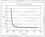
도 3은 폴리에틸렌 테레프탈레이트(polyethylene terephthalate; PET) 기판상의 은 나노와이어층의 흡수 스펙트럼을 예시한다.
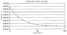
도 4는 와이어 직경에 기초한 나노와이어의 다양한 비저항 특성들에 대한 예상 값들을 예시하는 그래프이다.
도 5는 나노와이어들의 직경의 함수로 예상되는 전체 비저항을 예시하는 그래프이다.
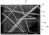
도 6은 두 개의 금속 콘택들 사이를 연결하는 단일의 은 나노와이어의 SEM 이미지를 나타낸다.
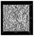
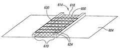
도 7은 투명 도전체를 위한 생물학적인 템플릿(template)으로 기능하는 섬유 단백질들(filamentous proteins)의 네트워크를 예시한다.
도 8은 다양한 결합 사이트들(binding sites)을 통해 도전 입자들에 결합된 단백질 골격(scaffold)을 예시한다.
도 9는 연관 펩티드들의 결합에 기초한 생물학적인 템플릿의 도전 네트워크 형성을 예시한다.
도 10a는 금속 나노와이어 기반의 투명 도전체의 일 실시예를 개략적으로 예시한다.
도 10b는 금속 나노와이어 기반의 투명 도전체의 다른 실시예를 개략적으로 예시한다.
도 10c는 나노와이어들의 부분들이 투명 도전체의 표면 상에 노출된 금속 나노와이어 기반의 투명 도전체의 또 다른 실시예를 개략적으로 나타낸다.
도 10d는 투명 도전체의 표면으로부터 돌출하는 은 나노와이어들의 SEM 이미지를 나타낸다.
도 10e는 금속 나노와이어 기반의 투명 도전체의 다른 실시예를 개략적으로 예시한다.
도 11은 다중층(multi-layer) 구조를 갖는 금속 나노와이어 기반의 투명 도전체의 또 다른 실시예를 개략적으로 예시한다.
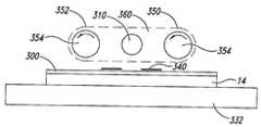
도 12는 기상 방지제(vapor phase inhibitor; VPI)를 공급하기 위한 저장부(reservoir)를 갖는 투명 도전체 구조체를 나타낸다.
도 13a~13d는 투명 도전체의 제조 공정의 일 예를 나타낸다.
도 14a는 웹 코팅(web coating)에 의한 투명 도전체 제조 공정의 일 예를 나타낸다.
도 14b는 웹 코팅(web coating)에 의한 투명 도전체 제조 공정의 다른 예를 나타낸다.
도 15a는 투명 도전체를 제조하기 위한 웹 코팅 시스템 및 흐름 공정(flow process)을 나타낸다.
도 15b는 압력 인가(pressure application)의 후처리(post-treatment) 뒤의 도전층의 SEM 이미지를 나타낸다.
도 16a-16b는 적층(lamination) 공정의 일 예를 나타낸다.
도 17a~17c는 적층 공정의 또 다른 예를 나타낸다.
도 18은 도전층을 광-패터닝하는 공정의 일 예를 나타낸다.
도 19a-19b는 웹 코팅 공정에 적합한 연속적인 광-패터닝 방법의 일 예를 나타낸다.
도 20은 패터닝된 투명 도전체를 제조하는 부분적인 시스템 및 공정을 나타낸다.
도 21은 금속 나노와이어들에 기초한 투명 전극들을 포함하는 디스플레이 장치를 나타낸다.
도 22는 금속 나노와이어들에 기초한 두 개의 투명 도전체들을 포함하는 터치 스크린(touch screen) 장치를 나타낸다.
도 23은 신선하게 요리된 계란 노른자위(cooked egg yolks)로부터의 H2S의 전형적인 방출 프로파일(release profile)을 나타낸다.
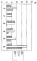
도 24a는 가속된 H2S 부식 테스트 전후의 6개의 샘플 도전막들의 광 투과성들(light transmissions)을 나타낸다.
도 24b는 가속된 H2S 부식 테스트 전후의 6개의 샘플 도전막들의 저항들을 나타낸다.
도 24c는 가속된 H2S 부식 테스트 전후의 6개의 샘플 도전막들의 헤이즈들(hazes)을 나타낸다.
도 25a는 나노와이어 기반의 투명 도전막을 직접 패터닝하는 공정의 일 예를 나타낸다.
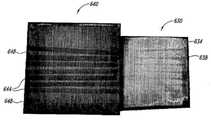
도 25b는 접착 테이프 처리(adhesive tape treatment) 전후의 패터닝된 도전막들의 사진을 나타낸다.
도 26a~26f는 다양한 배율 수준들에서 접착 테이프 처리 전후의 패터닝된 도전막들의 사진들을 나타낸다.
도 27a~27d는 용제처리(solvent treatment) 전후의 또 다른 대표적인 도전막의 사진들을 나타낸다.In the drawings, the same reference numbers identify similar components or actions. The size and relative position of components in the drawings are not necessarily drawn to scale. For example, the shapes and angles of the various components are not drawn to scale, and some of these components are arbitrarily enlarged and arranged to improve drawing readability. Furthermore, certain shapes of components as shown are not intended to convey any information regarding the actual shape of the particular components, and have been selected for ease of recognition only in the drawings.
1 is a schematic illustration of a nanowire.
2 is a graph illustrating the expected optical properties of silver nanoellipsoids at various wavelengths of light.
3 illustrates an absorption spectrum of a silver nanowire layer on a polyethylene terephthalate (PET) substrate.
4 is a graph illustrating expected values for various resistivity properties of nanowires based on wire diameter.
5 is a graph illustrating the overall resistivity expected as a function of the diameter of the nanowires.
6 shows an SEM image of a single silver nanowire connecting between two metal contacts.
FIG. 7 illustrates a network of filamentous proteins that function as biological templates for transparent conductors.
8 illustrates a protein scaffold bound to conductive particles through various binding sites.
9 illustrates the formation of a challenging network of biological templates based on the binding of related peptides.
10A schematically illustrates an embodiment of a metal nanowire-based transparent conductor.
10B schematically illustrates another embodiment of a metal nanowire-based transparent conductor.
10C schematically shows another embodiment of a metal nanowire-based transparent conductor in which portions of the nanowires are exposed on the surface of the transparent conductor.
10D shows an SEM image of silver nanowires protruding from the surface of a transparent conductor.
10E schematically illustrates another embodiment of a metal nanowire-based transparent conductor.
11 schematically illustrates another embodiment of a metal nanowire-based transparent conductor having a multi-layer structure.
12 shows a transparent conductor structure having a reservoir for supplying a vapor phase inhibitor (VPI).
13A to 13D show an example of a manufacturing process of a transparent conductor.
14A shows an example of a process for manufacturing a transparent conductor by web coating.
14B shows another example of a process for manufacturing a transparent conductor by web coating.
15A shows a web coating system and flow process for manufacturing a transparent conductor.
15B shows an SEM image of the conductive layer after post-treatment of pressure application.
16A-16B show an example of a lamination process.
17A to 17C show another example of the lamination process.
18 shows an example of a process of photo-patterning a conductive layer.
19A-19B show an example of a continuous light-patterning method suitable for a web coating process.
20 shows a partial system and process for manufacturing a patterned transparent conductor.
21 shows a display device including transparent electrodes based on metal nanowires.
22 shows a touch screen device comprising two transparent conductors based on metal nanowires.
23 shows a typical release profile of H2 S from freshly cooked egg yolks.
24A shows the light transmissions of the six sample conductive films before and after the accelerated H2 S corrosion test.
24B shows the resistances of the six sample conductive films before and after the accelerated H2 S corrosion test.
24C shows hazes of six sample conductive films before and after the accelerated H2 S corrosion test.
25A shows an example of a process of directly patterning a nanowire-based transparent conductive film.
25B shows photographs of patterned conductive films before and after adhesive tape treatment.
26A-26F show photographs of patterned conductive films before and after adhesive tape treatment at various magnification levels.
27A-27D show photographs of another representative conductive film before and after solvent treatment.
어떤 실시예들은 나노와이어들의 도전층에 기초한 투명 도전체를 나타낸다. 특히, 도전층은 금속 나노와이어들의 성긴(sparse) 네트워크를 포함한다. 나아가, 도전층은 투명하고 연성(flexible)이며, 도전성인 적어도 하나의 표면을 포함할 수 있다. 그것은 연성 및 경성(rigid) 기판들을 포함하여 다양한 기판들 상에 코팅 또는 적층될 수 있다. 도전층은 또한 매트릭스(matrix) 재료 및 나노와이어들을 포함하는 복합 구조체의 일부를 형성할 수 있다. 매트릭스 재료는 전형적으로 그러한 복합 구조체에 어떤 화학적, 기계적 그리고 광학적 특성들을 부여할 수 있다. 다른 실시예들은 도전층을 제조하고 패터닝하는 방법들을 설명한다.
Some embodiments represent a transparent conductor based on a conductive layer of nanowires. In particular, the conductive layer includes a sparse network of metal nanowires. Furthermore, the conductive layer may include at least one surface that is transparent, flexible, and conductive. It can be coated or laminated on a variety of substrates, including flexible and rigid substrates. The conductive layer can also form part of a composite structure comprising a matrix material and nanowires. Matrix materials can typically impart certain chemical, mechanical and optical properties to such composite structures. Other embodiments describe methods of manufacturing and patterning a conductive layer.
도전 나노와이어들(ConductiveConductive nanowiresNanowiresNanowires))
도 1은 길이(L1)를 직경(d1)으로 나눈 것과 동일한 종횡비(aspect ratio)를 갖는 나노와이어(2)를 나타낸다. 적절한 나노와이어들은 전형적으로 10 내지 100,000 범위 내의 종횡비들을 갖는다. 더 큰 종횡비들이 투명 도전체층을 얻기 위해 선호될 수 있는데, 그것들은 높은 투명성을 위해 와이어들의 더 낮은 전체 밀도를 허용하면서 더 효율적인 도전 네트워크들이 형성되도록 할 수 있기 때문이다. 달리 말하면, 높은 종횡비들을 갖는 도전 나노와이어들이 사용될 때, 도전 네트워크를 달성하는 나노와이어들의 밀도가 도전 네트워크가 실질적으로 투명하기에 충분히 낮을 수 있다.1 shows a
광에 대한 층의 투명도를 정의하는 하나의 방법은 그것의 흡수계수(absorption coefficient)에 의한 방법이다. 층을 통과하는 광의 조도(illumination)는 I = I0e-ax로 정의될 수 있는데, 여기서, I0는 그 층의 제1측 상에 들어온 광이고, I는 상기 층의 제2측 상에 존재하는 조도 수준이고, e-ax는 투명도 인자(transparency factor)이다. 투명도 인자에서, a는 흡수계수이고 x는 그 층의 두께이다. 1에 가까우나 1보다는 작은 투명도 인자를 갖는 층은 실질적으로 투명한 것으로 간주될 수 있다.One way to define the transparency of a layer to light is by its absorption coefficient. The illuminance of light passing through a layer can be defined as I = I0 e-ax , where I0 is light entering the first side of the layer, and I is on the second side of the layer. The level of illuminance present, and e-ax is the transparency factor. In the transparency factor, a is the absorption coefficient and x is the thickness of the layer. A layer close to 1 but with a transparency factor less than 1 can be considered substantially transparent.
도 2~5는 상기 도전 나노와이어들의 몇몇 광학적 전기적 특성들을 예시한다.2-5 illustrate some optical and electrical properties of the conductive nanowires.
도 2는 다양한 광 파장들에서 은(silver) 나노타원체들(nanoellipsoids)의 광 흡수에 대한 이론적 모델을 나타낸다. 폭 및 길이에 의존하여, 은 나노타원체들은 400과 440 나노미터 사이의 파장들에서 광의 좁은 대역에 대해 그리고 700nm 위의 광의 파장들에 대해 높은 소멸 계수(extinction coefficient)를 보인다. 그러나, 그것들은 가시 영역 내에 들어가는 약 440 내지 약 700nm 사이에서 실질적으로 투명하다.2 shows a theoretical model for light absorption of silver nanoellipsoids at various light wavelengths. Depending on the width and length, silver nanospheroids show high extinction coefficients for narrow bands of light at wavelengths between 400 and 440 nanometers and for wavelengths of light above 700 nm. However, they are substantially transparent between about 440 and about 700 nm entering the visible region.
도 3은 폴리에틸렌 테레프탈레이트(PET) 기판 상에 증착된 은 나노와이어들의 층의 흡수 스펙트럼을 나타낸다. 흡수 프로파일에 의해 보여지는 바와 같이, PET 기판 상의 은 나노와이어층은 약 440nm 내지 700nm 사이에서 실질적으로 투명하며, 도 2에서 보여진 이론적 모델의 결과들과 일치한다.3 shows the absorption spectrum of a layer of silver nanowires deposited on a polyethylene terephthalate (PET) substrate. As shown by the absorption profile, the silver nanowire layer on the PET substrate is substantially transparent between about 440 nm and 700 nm, consistent with the results of the theoretical model shown in FIG. 2.
도 4 및 5는 직경에 기초한 금속 나노와이어들의 비저항의 이론적 모델링 결과들을 나타낸다. 더 큰 직경의 나노와이어의 경우, 비록 더 많은 광을 흡수할 것이지만 비저항은 실질적으로 감소한다. 도 4에서 볼 수 있듯이, 결정립계(grain boundary) 및 표면산란(surface scattering)에 기초한 비저항에 대한 영향은 10nm 미만의 직경들에서 높다. 직경이 증가함에 따라, 이들 영향들은 급격히 감소된다. 그러므로, 전체 비저항은 직경이 10nm 에서 100nm로 증가하는 경우 상당히 감소된다(또한, 도 5 참조). 그러나 전기적 특성들의 향상은 투명 도전체를 필요로 하는 어플리케이션들을 위해 감소되는 투명도에 대해 균형을 이루어야 한다.4 and 5 show the theoretical modeling results of the specific resistance of metal nanowires based on diameter. In the case of larger diameter nanowires, the specific resistance is substantially reduced although it will absorb more light. As can be seen in FIG. 4, the effect on resistivity based on grain boundary and surface scattering is high at diameters less than 10 nm. As the diameter increases, these effects decrease rapidly. Therefore, the total resistivity is significantly reduced when the diameter increases from 10 nm to 100 nm (see also Fig. 5). However, the improvement in electrical properties must be balanced against reduced transparency for applications requiring transparent conductors.
도 6은 터미널(terminal) 6a에서부터 터미널 6b까지 전기적 도전 경로를 제공하기 위해 두 개의 다른 전기적 터미널들(6a 및 6b)을 연장하는 단일 은(Ag) 나노와이어(4)를 나타낸다. "터미널" 이라는 용어는 컨택 패드들, 도전 노드들(conduction nodes) 및 전기적으로 연결될 수 있는 시작 및 종료 점들을 포함한다. 종횡비, 크기, 형태 및 나노와이어들의 물리적 파라미터들의 분포는 원하는 광학적 전기적 특성들을 제공하도록 선택된다. 은 나노와이어들의 주어진 밀도를 제공할 그러한 와이어들의 숫자는 터미널 6a를 터미널 6b에 결합하기 위해 수용할 수 있는 전기적 도전 특성들을 제공하도록 선택된다. 예를 들면, 수 백 개의 은 나노와이어들(4)은 터미널 6a에서부터 터미널 6b로 낮은 저항의 전기 도전 경로를 제공하도록 연장될 수 있고, 농도(concentration), 종횡비, 크기 및 형태는 실질적으로 투명 도전체를 제공하도록 선택될 수 있다. 그러므로, 투명, 전기적 도전은 복수의 은 나노와이어들을 사용하여 터미널 6a로부터 터미널 6b로 제공된다.6 shows a single silver (Ag)
알 수 있는 바와 같이, 터미널 6a로부터 터미널 6b까지의 거리는 원하는 광학 특성들이 단일 나노와이어로써 얻어지지 않는 정도의 거리일 수 있다. 복수의 많은 나노와이어들은 터미널 6a로부터 터미널 6b까지 도전 경로를 제공하기 위해 다양한 지점들에서 서로에 대해 연결될 필요가 있을 수 있다. 본 발명에 따르면, 나노와이어들은 원하는 광학 특성들에 기초하여 선택된다. 그런 다음, 원하는 도전 경로와 그러한 경로 상에서의 전체 저항을 제공하는 나노와이어들의 숫자는 터미널 6a로부터 터미널 6b로 전기적 도전층을 위한 수용가능한 전기적 특성들을 달성하도록 선택된다.As can be seen, the distance from terminal 6a to terminal 6b may be such that the desired optical properties are not obtained with a single nanowire. Many of the plurality of nanowires may need to be connected to each other at various points to provide a conductive path from terminal 6a to terminal 6b. According to the present invention, nanowires are selected based on desired optical properties. Then, the number of nanowires that provide the desired conductive path and total resistance on that path is selected to achieve acceptable electrical properties for the electrically conductive layer from terminal 6a to terminal 6b.
투명층의 전기적 도전율은 주로 a)단일 나노와이어의 도전율, b)터미널들 사이의 나노와이어들의 숫자, 및 c)나노와이어들 사이의 연결성(connectivity)에 의해 주로 제어될 수 있다. 어떤 나노와이어 농도(또한 퍼컬레이션 스레스홀드(percolation threshold)로 불려지는) 이하에서, 터미널들 사이의 도전율은 영이다. 즉, 나노와이어들이 너무 멀리 떨어져 있기 때문에 제공되는 어떠한 연속적인 전류 경로도 없다.The electrical conductivity of the transparent layer can mainly be controlled by a) the conductivity of a single nanowire, b) the number of nanowires between terminals, and c) the connectivity between nanowires. Below a certain nanowire concentration (also called a percolation threshold), the conductivity between terminals is zero. That is, there is no continuous current path provided because the nanowires are too far apart.
도전 나노와이어들은 높은 종횡비들(예를 들어, 10보다 더 높은)을 갖는 금속 나노와이어들 및 다른 도전 입자들을 포함한다. 비금속 나노와이어들의 예들은 탄소 나노튜브들(carbon nanotubes;CNTs), 금속 산화 나노와이어들(metal oxide nanowires), 도전 중합체 섬유들(conductive polymer fibers) 등을 포함하지만, 이에 한정되지는 않는다.Conductive nanowires include metal nanowires with high aspect ratios (eg, higher than 10) and other conductive particles. Examples of non-metallic nanowires include, but are not limited to, carbon nanotubes (CNTs), metal oxide nanowires, conductive polymer fibers, and the like.
여기에서 사용되는 바와 같이, "금속 나노와이어(metal nanowire)"는 원소 금속(element metal), 금속 합금 또는 금속 혼합물(금속 산화물들을 포함)을 나타낸다. 적어도 하나의 금속 나노와이어의 단면의 크기는 500nm보다 적고, 200nm보다 적으며, 더 바람직하게는 100nm보다 더 적다. 위에서 언급한 바와 같이, 금속 나노와이어는 10보다 더 큰, 바람직하게는 50보다 더 큰, 그리고 더 바람직하게는 100보다 더 큰 종횡비(길이(length) : 폭(width))를 갖는다. 적절한 금속 나노와이어들은 은, 금, 구리, 니켈, 및 금도금된 은(gold-plated silver)을 포함하는 어떤 금속에 기초할 수 있으나, 이에 한정되지는 않는다.As used herein, “metal nanowire” refers to an element metal, metal alloy or metal mixture (including metal oxides). The size of the cross section of the at least one metal nanowire is less than 500 nm, less than 200 nm, and more preferably less than 100 nm. As mentioned above, the metal nanowires have an aspect ratio (length: width) greater than 10, preferably greater than 50, and more preferably greater than 100. Suitable metal nanowires can be based on, but are not limited to, any metal, including silver, gold, copper, nickel, and gold-plated silver.
금속 나노와이어들은 당해 기술분야에서 이미 알려진 방법들에 의해 제조될 수 있다. 특히, 은 나노와이어들은 폴리올(polyol)(예를 들어, 에틸렌 글리콜(ethylene glycol)) 및 폴리(비닐 피롤리돈(vinyl pyrrolidone))의 존재하에서 은염(silver salt)(예를 들어, 질산은(silver nitrate))의 액상환원법(solution-phase reduction)을 통해 합성될 수 있다. 균일한 크기의 은 나노와이어들의 대규모 제조는 예를 들면, Xia, Y.외, Chem. Mater.(2002), 14,4736-4745, 및 Xia, Y.외, Nanoletters(2003)3(7), 955-960에서 설명된 방법들에 따라서 제조될 수 있다.Metal nanowires can be made by methods already known in the art. In particular, silver nanowires are silver salts (e.g., silver nitrate) in the presence of polyols (e.g. ethylene glycol) and poly (vinyl pyrrolidone). nitrate)) can be synthesized through solution-phase reduction. Large scale production of uniformly sized silver nanowires can be performed, for example, in Xia, Y. et al., Chem. Mater. (2002), 14,4736-4745, and Xia, Y. et al., Nanoletters (2003) 3 (7), 955-960.
다르게는, 금속 나노와이어들은 광화(mineralized)될 수 있는 생물학적인 템플릿들(templates)(또는 생물학적인 골격들(scaffolds)를 사용하여 제조될 수 있다. 예를 들면, 바이러스들 및 파지들(phages)과 같은 생물학적인 재료들은 금속 나노와이어들을 생성하기 위해 템플릿들로서 기능할 수 있다. 어떤 실시예들에서, 생물학적인 템플릿들은 금속 또는 금속 산화물과 같은 특정 유형의 재료에 대한 선택적 친화력(affinity)을 표시하기 위해 계획될 수 있다. 나노와이어들의 생물학적 제조(biofabrication)에 관한 더 상세한 설명은 , 예를 들어, Mao, C.B. 외, "자기 및 반도체 나노와이어들의 직접 합성을 위한 바이러스 기반의 툴킷(Virus-based Toolkit for the Directed Synthesis of Magnetic and Semiconducting Nanowires,"(2004) 사이언스(Science), 303, 213-217. Mao, C.B.외, "양자 도트 나노와이어들을 이용한 바이러스성 어셈블리(Viral Assembly of Oriented Quantum Dot Nanowires),"(2003) PNAS, vol. 100, no. 12, 6946-6951; Mao, C.B.외, "양자 도트 나노와이어들을 이용한 바이러스성 어셈블리(Viral Assembly of Oriented Quantum Dot Nanowires),"(2003) PNAS, 100(12), 6946-6951, 미국 특허출원번호 10/976,179 및 미국 가출원번호 60/680,491에서 알 수 있고, 참고문헌들은 그 전체로서 본 명세서에 포함된다.Alternatively, metal nanowires can be made using biological templates (or biological scaffolds) that can be mineralized. For example, viruses and phages Biological materials such as can serve as templates to create metal nanowires In some embodiments, biological templates display a selective affinity for a particular type of material, such as a metal or metal oxide. For a more detailed description of the biofabrication of nanowires, see, for example, Mao, CB et al., "Virus-based Toolkit for Direct Synthesis of Magnetic and Semiconductor Nanowires. for the Directed Synthesis of Magnetic and Semiconducting Nanowires, "(2004) Science, 303, 213-217. Mao, CB et al.," Quantum Dot Nanowires Viral Assembly of Oriented Quantum Dot Nanowires, "(2003) PNAS, vol. 100, no. 12, 6946-6951; Mao, CB et al.," Viral Assembly Using Quantum Dot Nanowires of Oriented Quantum Dot Nanowires), "(2003) PNAS, 100 (12), 6946-6951, U.S. Patent Application No. 10 / 976,179 and U.S. Provisional Application No. 60 / 680,491, the references of which are incorporated herein in their entirety. Is included.
더 상세하게는, 도전 재료 또는 도전체(예를 들어, 금속 나노와이어)는 도전 재료와 생물학적인 템플릿 상에서 결합 사이트들(binding sites)(예를 들어, 펩티드 시퀀스들) 사이의 친화력에 근거하여 생물학적인 템플릿에 대해 직접적으로 결합할 수 있다.More specifically, the conductive material or conductor (eg, metal nanowire) is based on the affinity between the conductive material and binding sites (eg, peptide sequences) on the biological template. You can combine directly with the in-template.
다른 실시예들에서, 도전 재료는 결정핵생성(nucleation) 공정에 의해 생성될 수 있고, 그동안 전구체(precursor)는 생물학적인 템플릿들에 대해 결합하는 도전 입자들로 변환되고, 그 도전 입자들은 나아가 연속적인 도전층으로 성장할 수 있다. 이러한 공정은 "광화(mineralization)" 또는 "도금(plating)"으로 또한 불려진다. 예를 들어, 금속 전구체(예를 들어, 금속염(metal salt))는 환원제(reducing agent)의 존재하에 원소 금속으로 변환될 수 있다. 결과적인 원소 금속은 생물학적인 템플릿들에 대해 결합하고 연속적인 금속층으로 성장한다.In other embodiments, the conductive material can be produced by a nucleation process, during which the precursor is converted into conductive particles that bind to biological templates, the conductive particles going further Can grow as a conductive layer. This process is also referred to as "mineralization" or "plating". For example, metal precursors (eg, metal salts) can be converted to elemental metals in the presence of a reducing agent. The resulting elemental metal binds to biological templates and grows into a continuous metal layer.
다른 실시예들에서, 시드(seed) 재료층은 초기에 생물학적인 재료 상에서 결정핵생성된다. 그 후에, 금속 전구체는 금속으로 변환될 수 있고, 그러한 시드 금속층 상에 도금된다. 예를 들어, 시드 재료는 결정핵생성 및 상응하는 금속 전구체를 포함하는 용액(solution)으로부터 금속의 성장을 일으키는 재료에 기초하여 선택될 수 있다. 예를 들어, 팔라듐(palladium)을 포함하는 시드 재료층은 구리(Cu) 또는 금(Au)의 광화를 일으킬 수 있다. 하나의 특정 예로서, 구리 도전체를 생성하기 위해 수용가능한 시드 재료들은 팔라듐, 팔라듐 기반의 분자, 금 또는 금 기반의 분자를 포함할 수 있다. 산화 도전체로서, 산화 아연은 결정핵생성 재료로서 사용될 수 있다. 시드 재료의 예들은 니켈(Ni), 구리(Cu), 팔라듐(Pd), 코발트(Co), 백금(Pt), 루테늄(Ru), 은(Ag), 코발트 합금들 또는 니켈 합금들을 포함한다. 도금될 수 있는 금속들, 금속 합금들 및 금속 산화물들은 구리, 금, 은, 니켈, 팔라듐, 코발트, 루테늄, 텅스텐(W), 크롬(Cr), 몰리브덴(Mo), 은, 코발트 합금들(예, 코발트-백금(CoPt)), 니켈 합금들, 철 합금들(예, 철-백금(FePt)) 또는 이산화티타늄(TiO2), 산화코발트(Co3O4), 산화구리(Cu2O), 이산화하프늄(HfO2), 산화아연(ZnO), 산화 바나듐(vanadium oxides), 산화 인듐(indium oxide), 산화 알루미늄, 산화 인듐주석(indium tin oxide), 산화 니켈(nickle oxide), 산화 구리, 산화 주석, 산화 탄탈륨(tantalum oxide), 산화 니오브(niobium oxide), 산화 바나늄 또는 산화 지르코늄(zirconium oxide)을 포함하지만, 이에 한정되지는 않는다.
In other embodiments, the seed material layer is initially nucleated on a biological material. Thereafter, the metal precursor can be converted to a metal and plated on such a seed metal layer. For example, the seed material can be selected based on the material that causes nucleation and growth of the metal from a solution comprising the corresponding metal precursor. For example, a layer of seed material comprising palladium may cause mineralization of copper (Cu) or gold (Au). As one specific example, seed materials that are acceptable to create a copper conductor may include palladium, palladium based molecules, gold or gold based molecules. As an oxidizing conductor, zinc oxide can be used as a nucleation material. Examples of seed material include nickel (Ni), copper (Cu), palladium (Pd), cobalt (Co), platinum (Pt), ruthenium (Ru), silver (Ag), cobalt alloys or nickel alloys. Metals, metal alloys and metal oxides that can be plated are copper, gold, silver, nickel, palladium, cobalt, ruthenium, tungsten (W), chromium (Cr), molybdenum (Mo), silver, cobalt alloys (eg , Cobalt-platinum (CoPt), nickel alloys, iron alloys (eg, iron-platinum (FePt)) or titanium dioxide (TiO2 ), cobalt oxide (Co3 O4 ), copper oxide (Cu2 O) , Hafnium dioxide (HfO2 ), zinc oxide (ZnO), vanadium oxides, indium oxide, aluminum oxide, indium tin oxide, nickel oxide, copper oxide, Tin oxide, tantalum oxide, niobium oxide, vanadium oxide, or zirconium oxide.
복수의 상이한 생물학적인 재료들 중의 어떤 것은 단백질들(proteins), 펩티드들, 파지들, 박테리아들, 바이러스들 등을 생성하기 위한 템플릿들을 제공하기 위해 사용될 수 있다. 원하는 금속 또는 도전 재료에 대해 결합할 생물학적인 재료를 선택, 형성 및 처리하기 위한 기술들은 미국 특허출원번호 10/155,883 및 10/158,596에서 설명되어 있고, 양 특허출원들은 출원인이 캄브리오스 테크놀로지 코퍼레이션(Cambrios Technologies corporation)이고 본 명세서에 참고로 포함된다.Any of a plurality of different biological materials can be used to provide templates for generating proteins, peptides, phages, bacteria, viruses, and the like. Techniques for selecting, forming and processing a biological material to bind to a desired metal or conductive material are described in U.S. Patent Application Nos. 10 / 155,883 and 10 / 158,596, both of which are filed by the applicant at Cambrios Technology Corporation (Cambrios Technologies corporation) and incorporated herein by reference.
위에서 언급한 바와 같이, 단백질, 펩티드와 같은 생물학적인 템플릿들, 또는 다른 생물학적인 재료는 선택된 시드 재료 또는 선택된 도전 재료를 위해 친화력 사이트들을 갖도록 처리될 수 있다. 특정 재료에 대해 친화력을 갖는 단백질들 또는 펩티드들은 파지 표시, 이스트(yeast) 표시, 셀 표면 표시 또는 그 밖의 것들과 같은 단백질 발견 공정을 통해 식별될 수 있다. 파지 표시의 경우에 있어서 예를 들어, 파지들의 라이브러리들(예, M13 파지들)은 다양한 상이한 시퀀스들의 펩티드들을 파지 개체군 내에 삽입함으로써 생성될 수 있다. 특정 목표의 분자에 대해 높은 친화력을 갖는 단백질은 격리될 수 있고 그의 펩티드 구조체가 식별될 수 있다.As mentioned above, biological templates such as proteins, peptides, or other biological materials can be treated to have affinity sites for the selected seed material or selected conductive material. Proteins or peptides that have affinity for a particular material can be identified through protein discovery processes such as phage labeling, yeast labeling, cell surface labeling or the like. In the case of phage display, for example, libraries of phages (eg, M13 phages) can be generated by inserting peptides of various different sequences into a phage population. Proteins with high affinity for a particular target molecule can be isolated and their peptide constructs can be identified.
특히, 생물학적인 분자들의 유전자 시퀀스들은 어떤 유형의 파지 입자들에서 복수의 특정 펩티드 시퀀스들의 카피들(copies)을 제공하도록 제어될 수 있다. 예를 들어, P8 단백질들의 약 3000 카피들은 M13 파지 입자들의 길이에 따른 순서화된 배열 내에 정렬될 수 있다. P8 단백질들은 도전 재료의 구성(formation)을 결정핵생성하거나 도전 재료를 결합하여, 그에 의해 높은 도전성의 도전 나노와이어들을 제공할 수 있는 특정 펩티드 시퀀스를 포함하도록 변형(modify)될 수 있다. 바람직하게는, 이러한 기술은 생물학적인 템플릿 분자들, 예를 들면, 특별히 설계되거나 제어되는 펩티드 시퀀스들을 갖는 단백질들의 사용을 통한 나노와이어들의 기하학적 및 결정 구조체를 제어할 수 있는 기능들을 허용한다. 그 때문에, 은, 금 또는 팔라듐(palladium)에 대해 결합 친화력을 갖는 펩티드들 또는 단백질들은 어느 것이 파지 입자들의 크기에 기초한 크기들을 갖는 나노와이어들을 생성하기 위해 파지 구조체 내에 통합될 수 있는 지 식별되어 왔다.In particular, the genetic sequences of biological molecules can be controlled to provide copies of a plurality of specific peptide sequences in certain types of phage particles. For example, about 3000 copies of P8 proteins can be arranged in an ordered arrangement along the length of the M13 phage particles. P8 proteins can be modified to include a specific peptide sequence that can nucleate the formation of the conductive material or combine the conductive material, thereby providing highly conductive conductive nanowires. Preferably, this technique allows the ability to control the geometry and crystal structure of nanowires through the use of biological template molecules, for example proteins with specially designed or controlled peptide sequences. To that end, peptides or proteins with binding affinity for silver, gold or palladium have been identified which can be incorporated into the phage construct to produce nanowires with sizes based on the size of the phage particles. .
파지 이외의 생물학적인 재료들이 도전 나노와이어들의 구성을 위해 템플릿들로서 사용될 수 있다. 예를 들면, 수십 마이크론 길이의 긴 스트랜드들(strands) 내에서 자기회합(self-assemble)하는 섬질 단백질들(filamentous proteins)이 대체 템플릿으로서 사용될 수 있다(도 7 참조). 바람직하게는, 그러한 템플릿 단백질은 파지보다 훨씬 더 큰 종횡비를 갖도록 합성될 수 있으며, 그것은 더 낮은 도전 나노와이어들의 퍼컬레이션 스레스홀드(percolative threshold) 농도들로 유도한다. 또한, 단백질들은 대량으로 합성하기에 파지 입자들보다 더 용이하다. 세제 첨가물들로 사용되는 효소들과 같은 단백질들의 대량 제조는 잘 발전되어 있다.Biological materials other than phage can be used as templates for the construction of conductive nanowires. For example, filamentous proteins that self-assemble within tens of microns long strands can be used as an alternative template (see Figure 7). Preferably, such a template protein can be synthesized to have an aspect ratio much greater than the phage, which leads to percolative threshold concentrations of lower conducting nanowires. In addition, proteins are easier to synthesize than phage particles to synthesize in large quantities. Mass production of proteins, such as enzymes used as detergent additives, is well developed.
도 8은 도전 입자들(8b)에 결합된 많은 결합 사이트들(8a)을 갖는 단백질 골격(scaffold)의 개략도이다. 결합 사이트들은 금(Au), 은(Ag), 구리(Cu) 및 니켈(Ni)과 같은 도전 입자들에 대해 친화력을 갖도록 선택된다. 다르게는, 결합 사이트들(8a)은 구리 등과 같은 도전 입자들을 더 결정핵생성할 수 있는 시드 재료층(예를 들면, 팔라듐(Pd) 및 금(Au))에 대한 친화력을 갖는다. 단백질 골격(8)은 또한 그러한 친화력을 갖는 복수의 결합 사이트들(8a)을 갖도록 처리될 수 있다. 최종 도전층의 도전성을 증가시키기 위해 그들의 길이를 따라 그들이 많게 그리고 규칙적인 간격으로 떨어지도록 하는 것이 더 바람직하다.8 is a schematic diagram of a protein scaffold with many
단백질과 같은 생물학적인 재료의 길이 뿐만 아니라 그 직경도 공지된 기술들을 사용하여 쉽게 처리된다. 광학적 특성들을 위한 정확한 크기들을 갖도록 처리된다. 크기, 형태 및 종횡비가 선택된 경우, 생물학적인 재료는 금속, 또는 금속의 전구체와 같은 도전 재료(8b)에 노출될 수 있다.The length of the biological material, such as protein, as well as its diameter, are readily processed using known techniques. It is processed to have the correct sizes for the optical properties. If size, shape and aspect ratio are selected, the biological material can be exposed to a
도 9는 생물학적인 템플릿들을 사용하는 도전 나노와이어들을 제조하는 또 다른 실시예를 나타낸다. 단백질 골격(8)은 연관 펩티드들(9a 및 9b)의 각각의 단(end)과 같은 결합 파트너들을 포함하도록 더 처리될 수 있다. 결합 파트너들은, 예를 들면, 이온 결합(ionic interaction), 공유 결합(covalent bonding), 수소 결합(hydrogen bonding), 소수성 결합(hydrophobic interaction) 등을 포함하는 어떤 유형의 연관 상호작용을 통하여 서로 간에 결합될 수 있다. 도 8에서의 최종 시퀀스에서 보여지는 바와 같이, 연관 펩티드들(9a 및 9b) 사이의 상호작용은 2-D 상호연결된 망 네트워크들 내로 도전 나노와이어들의 자기회합(self-assembly)을 촉진한다. 연관 펩티드들 및 그들의 로케이션들은 망들(meshes)의 형성, 단대단(end to end) 연결, 교차연결들, 그리고 도전층을 위한 다른 원하는 유형들을 촉진하기 위한 유형을 가질 수 있다. 도 8에서 보여지는 예에서, 도전 재료(8b)는 단백질 골격들이 네트워크를 형성하기 전에 단백질 골격(8)에 대해 이미 결합되어 있다. 단백질 골격(8)은 또한 도전 재료의 결합 이전에 네트워크를 형성할 수 있다.9 shows another embodiment of manufacturing conductive nanowires using biological templates. The
따라서 연관 펩티드들 또는 다른 결합 파트너들을 갖는 생물학적인 템플릿의 사용은 임의(random) 나노와이어들로써 가능한 것보다 더 단단히 연결된 네트워크의 도전층의 형성을 허용한다. 그러므로 생물학적인 템플릿들의 특정 네트워크는 도전층에서 원하는 정도의 순서를 달성하도록 선택될 수 있다.Thus, the use of biological templates with associated peptides or other binding partners allows the formation of a conductive layer of a more tightly coupled network than is possible with random nanowires. Therefore, a specific network of biological templates can be selected to achieve the desired degree of ordering in the conductive layer.
템플릿 기반의 합성(template-based synthesis)은 특히 특정 크기들, 형태들(morphologies) 및 구조들(compositions)의 나노와이어들을 제조하기에 특히 적합하다. 생물할적인 기반의 나노-재료들의 제조의 추가 이점들은, 높은 처리율, 주위 온도 증착(ambient temperature deposition), 도전층의 우수한 합성(superior conformality) 및 생성을 위해 변경될 수 있는 용액(solution) 처리를 포함한다.
Template-based synthesis is particularly suitable for manufacturing nanowires of specific sizes, morphologies and compositions. Additional advantages of the production of bio-half based nano-materials include high throughput, ambient temperature deposition, superior conformality of the conductive layer and solution processing that can be altered for production. Includes.
도전층Conductive layer 및 기판(Conductive Layer and Substrate) And substrate (Conductive Layer and Substrate)
예시된 바와 같이, 도 10a는 기판(14) 상에 코팅된 도전층(12)을 포함하는 투명 도전체(10)를 보여준다. 도전층(12)은 복수의 금속 나노와이어들(16)을 포함한다. 금속 나노와이어들은 도전 네트워크를 형성한다.As illustrated, FIG. 10A shows a
도 10b는 투명 도전체(10')의 다른 예를 나타내며, 여기서 도전층(12')은 기판(14) 상에 형성된다. 도전층(12')은 매트릭스(18) 내에 매몰된 복수의 나노와이어들(16)을 포함한다.10B shows another example of the transparent conductor 10 ', where the conductive layer 12' is formed on the
"매트릭스"는 내부에 금속 나노와이어들이 산재되어 있거나 매몰되어 있는 고체 상태 재료(solid-state material)를 나타낸다. 나노와이어들의 일부는 도전 네트워크에 대해 억세스하도록 하기 위해 매트릭스 재료로부터 돌출(protrude)될 수 있다. 매트릭스는 부식 및 마모와 같은 나쁜 환경적 인자들로부터 금속 나노와이어들을 보호한다. 특히, 매트릭스는 습기, 극소량의 산(acid), 산소, 황 등과 같은 환경에서 부식 성분들의 투과율을 상당히 낮출 수 있다."Matrix" refers to a solid-state material in which metal nanowires are interspersed or buried. Some of the nanowires can be extruded from the matrix material to allow access to the conductive network. The matrix protects metal nanowires from bad environmental factors such as corrosion and wear. In particular, the matrix can significantly lower the permeability of corrosive components in environments such as moisture, trace amounts of acid, oxygen, sulfur, and the like.
또한, 매트릭스는 도전층에 대해 유리한 물리적 기계적 특성들을 제공한다. 예를 들면, 그것은 피란에 대해 접착력을 제공할 수 있다. 나아가, 금속 산화막들과는 달리, 금속 나노와이어들이 매몰된 중합체 매트릭스들 또는 유기 매트릭스들은 강하고(robust) 연성(flexible)일 수 있다. 여기서 더 상세히 논의되겠지만, 연성 매트릭스들은 저비용, 고 처리량 공정에서 투명 도전체들을 제조하는 것을 가능하게 한다.In addition, the matrix provides advantageous physical and mechanical properties to the conductive layer. For example, it can provide adhesion to pyran. Furthermore, unlike metal oxide films, polymer matrices or organic matrices in which metal nanowires are buried may be robust and flexible. As will be discussed in more detail herein, flexible matrices make it possible to fabricate transparent conductors in a low cost, high throughput process.
나아가, 도전층의 광학적 특성들은 적절한 매트릭스 재료를 선택함으로써 조절될 수 있다. 예를 들어, 반사 손실(reflection loss) 및 원하지 않은 섬광은 바람직한 굴절률(refractive index), 구성 및 두께를 갖는 매트릭스를 사용함으로써 효과적으로 감소될 수 있다.Furthermore, the optical properties of the conductive layer can be adjusted by selecting an appropriate matrix material. For example, reflection loss and unwanted glare can be effectively reduced by using a matrix with the desired refractive index, composition and thickness.
전형적으로는, 매트릭스는 광학적으로 투명한 재료이다. 재료는 만약 재료의 광 투과율이 가시 영역(400nm - 700nm) 내에서 적어도 80%라면 광학적으로 투명한 것으로 여겨진다. 하지만 만약 명기되지 않더라도, 여기에서 설명되는 투명 도전체에서의 모든 층들(기판을 포함하여)이 광학적으로 투명한 것이 바람직하다. 매트릭스의 광학적 투명성은 전형적으로는 굴절률(refractive index;RI), 두께, 두께 전체의 RI의 밀도(consistency), 표면(인터페이스를 포함하여) 반사, 및 헤이즈(haze)(표면 거칠기(roughness) 및/또는 매몰된 입자들에 기인하는 산란 손실(scattering loss)) 등의 다수의 인자들에 의해 결정되나, 이에 한정되지는 않는다.Typically, the matrix is an optically transparent material. The material is considered optically transparent if the light transmittance of the material is at least 80% in the visible region (400nm-700nm). However, if not specified, it is preferred that all layers (including the substrate) in the transparent conductor described herein are optically transparent. The optical transparency of the matrix is typically refractive index (RI), thickness, density of RI throughout the thickness, surface (including interface) reflection, and haze (surface roughness and / or Or it is determined by a number of factors, such as scattering loss (scattering loss) due to the buried particles, but is not limited thereto.
어떤 실시예들에서, 매트릭스는 약 10 nm 내지 5㎛ 두께, 약 20 nm 내지 1㎛ 두께, 또는 약 50 nm 내지 200 nm 두께이다. 다른 실시예들에서, 매트릭스는 약 1.3 내지 2.5, 또는 약 1.35 내지 1.8의 굴절률을 갖는다.In some embodiments, the matrix is about 10 nm to 5 μm thick, about 20 nm to 1 μm thick, or about 50 nm to 200 nm thick. In other embodiments, the matrix has a refractive index of about 1.3 to 2.5, or about 1.35 to 1.8.
어떤 실시예들에서, 매트릭스는 중합체이고, 이는 또한 중합체 매트릭스(polymeric matrix)로서 불려진다. 광학적으로 투명한 중합체들은 당해 기술 분야에서 알려져 있다. 적절한 중합체 매트릭스들의 예들은, 폴리메타크릴레이트(polymethacrylates)(예, 폴리(메틸 메타크릴레이트)(poly(methyl methacrylate)))와 같은 폴리아크릴들(polyacrylics), 폴리아크릴레이트들(polyacrylates) 및 폴리아크릴로니트릴들(polyacrylonitriles), 폴리비닐 알코올들(polyvinyl alcohols), 폴리에스테르(polyesters)(예, 폴리에틸렌 테레프탈레이트(polyethylene terephthalate(PET)), 폴리에스테르 나프탈레이트(polyester naphthalate), 및 폴리카보네이트들(polycarbonates)), 페놀들(phenolics) 또는 크레졸-포름알데히드(cresol-formaldehyde)(Novolacs®)와 같은 고차 방향족(aromaticity)을 갖는 중합체들, 폴리스티렌들(polystyrenes), 폴리비닐톨루엔(polyvinyltoluene), 폴리비닐크실렌(polyvinylxylene), 폴리이미드들, 폴리아미드들(polyamides), 폴리아미드이미드들(polyamideimides), 폴리에테르이미드들(polyetherimides), 폴리술파이드들(polysulfides), 폴리술폰들(polysulfones), 폴리페닐렌들(polyphenylenes), 및 폴리페닐 에테르들(polyphenyl ethers), 폴리우레탄(polyurethane;PU), 에폭시(epoxy), 폴리올레핀들(polyolefins)(예, 폴리프로필렌(polypropylene), 폴리메틸펜텐(polymethylpentene), 및 환형 올레핀들(cyclic olefins)), 아크릴로니트릴-부타디엔-스티렌 공중합체(acrylonitrile-butadiene-styrene copolymer;ABS), 셀룰로오스 화합물들(cellulosics), 실리콘들(silicones) 및 그 밖의 중합체들을 포함하는 실리콘(예, 폴리실세스퀴옥산들(polysilsesquioxanes) 및 폴리실란들(polysilanes)), 폴리염화비닐(polyvinylchloride;PVC), 폴리아세테이트들(polyacetates), 폴리노보넨들(polynorbornenes), 합성 고무들(synthetic rubbers)(예, EPR, SBR, EPDM), 및 불소중합체들(fluoropolymers)(예, 폴리불화비닐리덴(polyvinylidene fluoride), 폴리테트라플루로에틸렌(polytetrafluoreoethylene;TFE) 또는 폴리헥사플루로프로필렌(polyhexafluoropropylene), 플루로-올레핀(fluoro-olefin)과 탄화수소 올레핀(hydrocarbon olefin)(예, Lumiflon®), 및 무정형(amorphous) 불화탄소(fluorocarbon) 중합체들 또는 공중합들(예, 아사히 글래스사(Asahi Glass Co.)의 CYTOP®,또는 듀퐁(Du Pont)의 Teflon® AF)을 포함하지만, 이에 한정되지는 않는다.In some embodiments, the matrix is a polymer, which is also referred to as a polymeric matrix. Optically transparent polymers are known in the art. Examples of suitable polymer matrices include polyacrylics, polyacrylates and polyacrylates such as polymethacrylates (e.g. poly (methyl methacrylate)). Acrylonitriles, polyvinyl alcohols, polyesters (e.g. polyethylene terephthalate (PET)), polyester naphthalate, and polycarbonates ( polycarbonates), polymers with higher aromatics such as phenolics or cresol-formaldehyde (Novolacs® ), polystyrenes, polyvinyltoluene, polyvinyl Polyvinylxylene, polyimides, polyamides, polyamideimides, polyetherimides, polysulfes Polysulfides, polysulfones, polyphenylenes, and polyphenyl ethers, polyurethane, PU, epoxy, polyolefins ( Examples: polypropylene, polymethylpentene, and cyclic olefins, acrylonitrile-butadiene-styrene copolymer (ABS), cellulose compounds (cellulosics) ), Silicones containing silicones and other polymers (e.g. polysilsesquioxanes and polysilanes), polyvinylchloride (PVC), polyacetates ), Polynorbornenes, synthetic rubbers (e.g. EPR, SBR, EPDM), and fluoropolymers (e.g. polyvinylidene fluoride, polytetrafluro) Ethylene (polytetrafluoreoethylene; TFE) Or polyhexafluoropropylene, fluoro-olefins and hydrocarbon olefins (e.g. Lumiflon® ), and amorphous fluorocarbon polymers or copolymers (e.g. , CYTOP® from Asahi Glass Co., or Teflon® AF from Du Pont).
다른 실시예들에서, 매트릭스는 무기 재료(inorganic material)이다. 예를 들어, 실리카(silica), 멀라이트(mullite), 알루미나(alumina), SiC, MgO-Al2O3-SiO2, Al2O3-SiO2, MgO-Al2O3-SiO2-Li2O 또는 그들의 혼합물에 근거한 졸-겔(sol-gel) 매트릭스가 사용될 수 있다.In other embodiments, the matrix is an inorganic material. For example, silica, mullite, alumina, SiC, MgO-Al2 O3 -SiO2 , Al2 O3 -SiO2 , MgO-Al2 O3 -SiO2- Sol-gel matrices based on Li2 O or mixtures thereof can be used.
어떤 실시예들에서, 매트릭스 자체가 도전성이다. 예를 들어, 매트릭스는 도전 중합체일 수 있다. 도전 중합체들은 폴리(3, 4-에틸렌디옥시티오핀(3, 4-ethylenedioxythiophene)(PEDOT), 폴라아닐린들(polyanilines), 폴리티오핀들(polythiophenes), 및 폴리디아세틸렌들(polydiacetylenes)을 포함하여 당해 기술 분야에서 잘 알려져 있으며, 이에 한정되지는 않는다.In some embodiments, the matrix itself is conductive. For example, the matrix can be a conductive polymer. Conductive polymers include poly (3, 4-ethylenedioxythiophene (PEDOT), polyanilines, polythiophenes, and polydiacetylenes It is well known in the art, but is not limited thereto.
"도전층", 또는 "도전막"은 투명 도전체의 도전 매체를 제공하는 금속 나노와이어의 네트워크층을 말한다. 매트릭스가 존재할 때, 금속 나노와이어들의 네트워크층과 매트릭스의 조합이 "도전층"으로 또한 불려진다. 도전성은 하나의 금속 나노와이어로부터 다른 하나의 금속 나노와이어까지의 전하 퍼컬레이션(electrical charge percolation)에 의해 달성되고, 충분한 금속 나노와이어들은 전기적 퍼컬레이션 스레스홀드(electrical percolation threshold)에 도달하고 도전성이 되도록 하기 위해 도전층에 존재해야 한다. 도전층의 표면 도전성은 그의 표면 비저항(종종 시트 저항(sheet resistance)으로 일컬어짐)에 반비례하고, 이는 당해 기술 분야에서 공지된 방법들에 의해 측정될 수 있다."Conductive layer", or "conductive film" refers to a network layer of metal nanowires that provide a conductive medium of a transparent conductor. When the matrix is present, the combination of the network layer of the metal nanowires and the matrix is also referred to as the “conductive layer”. Conductivity is achieved by electrical charge percolation from one metal nanowire to another metal nanowire, and sufficient metal nanowires reach an electrical percolation threshold and conductivity To be possible, it must be present in the conductive layer. The surface conductivity of the conductive layer is inversely proportional to its surface resistivity (often referred to as sheet resistance), which can be measured by methods known in the art.
마찬가지로, 매트릭스가 존재할 때, 매트릭스는 도전성이 되도록 충분한 금속 나노와이어들로써 채워져야 한다. 여기에서 사용되는 바와 같이 "스레스홀드 로딩 레벨(threshold loading level)"은 도전층이 약 106 Ω/제곱(또는 Ω/□)보다 크지 않은 표면 비저항을 갖는 도전층의 로딩이후에 중량(weight)에 있어서 금속 나노와이어들의 백분율을 말한다. 스레스홀드 로딩 레벨은 종횡비, 얼라인먼트(alignment)의 정도, 집적(agglomeration)의 정도 및 금속 나노와이어들의 비저항과 같은 인자들에 기초한다.Likewise, when a matrix is present, the matrix must be filled with sufficient metal nanowires to be conductive. As used herein, "threshold loading level" is the weight after loading of the conductive layer having a surface resistivity of which the conductive layer is not greater than about 106 Ω / square (or Ω / □). ) Is the percentage of metal nanowires. The threshold loading level is based on factors such as aspect ratio, degree of alignment, degree of agglomeration, and resistivity of metal nanowires.
당해 기술 분야에서 숙련된 자에 의해 이해되는 바와 같이, 매트릭스의 기계적 광학적 특성들은 거기서의 어떤 입자들의 높은 로딩에 의해 대체되거나 절충(compromise)되는 경향이 있다. 바람직하게는, 금속 나노와이어들의 높은 종횡비들은 바람직하게는 은 나노와이어들에 대해서 약 0.05㎍/cm2 내지 약 10㎍/cm2, 더 바람직하게는, 약 0.1㎍/cm2 내지 약 5㎍/cm2, 그리고 더 바람직하게는 약 0.8㎍/cm2 내지 약 3㎍/cm2의 스레스홀드 표면 로딩 레벨에서 매트릭스를 통해 도전 네트워크의 형성을 허용한다. 이러한 표면 로딩 레벨들은 매트릭스의 기계적 또는 광학적 특성들에는 영향을 미치지 않는다. 이러한 값들은 나노와이어들의 크기들 및 공간 분산(dispersion)에 강하게 의존한다. 바람직하게는, 조정가능한 전기적 전도성(또는 표면 비저항)의 투명 도전체들 및 광학적 투명성은 금속 나노와이어들의 로딩 레벨들을 조정함으로써 제공될 수 있다.As understood by those skilled in the art, the mechanical and optical properties of the matrix tend to be replaced or compromised by the high loading of certain particles there. Preferably, the high aspect ratio of the metal nanowires are preferably from about 0.05㎍ / cm2 to have from about 10㎍ / cm2, more preferably, from about 0.1㎍ / cm2 to about the nanowire about 5㎍ / cm2 , and more preferably from about 0.8 μg / cm2 to about 3 μg / cm2 , allows formation of a conductive network through the matrix at a threshold surface loading level. These surface loading levels do not affect the mechanical or optical properties of the matrix. These values strongly depend on the size and spatial dispersion of the nanowires. Preferably, adjustable electrical conductivity (or surface resistivity) transparent conductors and optical transparency can be provided by adjusting the loading levels of the metal nanowires.
어떤 실시예들에서, 도전층은 도 10b에서 보여지는 바와 같이 매트릭스의 전체 두께에 걸쳐있다. 바람직하게는, 금속 나노와이어들의 어떤 부분은 매트릭스 재료(예, 중합체들)의 표면 장력(surface tension)에 기인하여 매트릭스의 표면(19) 상에 노출(expose)된다. 이러한 특징은 특히 터치 스크린 어플리케이션들에서 유용한다. 특히, 투명 도전체는 거기서의 적어도 하나의 표면 상에서 표면 도전성을 표시한다. 도 10c는 매트릭스에 매몰된 금속 나노와이어들의 네트워크가 표면 도전성을 어떻게 달성하는지를 나타낸다. 보여지는 바와 같이, 나노와이어(16a)와 같은 어떤 나노와이어들이 매트릭스(18) 내에 완전히 '침지(submerged)'될 수 있는 반면, 단(16b)과 같은 다른 나노와이어들의 단들은 매트릭스(18)의 표면(19) 상부로 돌출한다. 또한, 중간 섹션(16c)과 같은 나노와이어들의 중간 섹션의 부분은 매트릭스(18)의 표면(19)의 밖으로 돌출할 수 있다. 만약 충분한 나노와이어 엔드들(16b)과 중간 섹션들(16c)이 매트릭스 상부로 돌출한다면, 투명 도전체의 표면은 도전성이 된다. 도 10d는 투명 도전체에서 매트릭스 상으로 돌출하는 나노와이어들의 단들 및 중간 섹션들의 윤곽을 보여주는 투명 도전체의 일 실시예의 표면의 SEM(scanning electron micrograph)이다.In some embodiments, the conductive layer spans the entire thickness of the matrix as shown in FIG. 10B. Preferably, some portion of the metal nanowires is exposed on the
다른 실시예들에서, 도전층은 도 10e에 보여지는 바와 같이, 매트릭스의 일부에 매몰된 금속 나노와이어들에 의해 형성된다. 도전층(12'')는 매트릭스(18)의 단지 일부를 차지하며 완전히 매트릭스(18) 내에 "침지"되어 있다.In other embodiments, the conductive layer is formed by metal nanowires buried in a portion of the matrix, as shown in FIG. 10E. The
"기판", 또는 "선택된 기판(substrate of choice)"은 그 상에 도전층이 코팅되거나 적층되는 재료를 말한다. 기판은 경성(rigid) 또는 연성(flexible)일 수 있다. 기판은 투명 또는 불투명일 수 있다. "선택된 기판"이라는 용어는, 여기에서 논의될 바와 같이, 전형적으로 적층 공정(lamination process)과 관련하여 사용된다. 적절한 경성 기판들은, 예를 들면 글래스, 폴리카보네이트, 아크릴 등을 포함한다. 적절한 연성 기판들은 폴레에스테르(예, 폴리에틸렌 테레프탈레이트(PET), 폴리에스테르 나프탈레이트, 및 폴리카보네이트), 폴리올레핀(예, 선형, 분지(brancned), 및 환형 폴리올레핀), 폴리비닐(예, 폴리염화비닐, 폴리염화비닐리덴, 폴리비닐 아세탈, 폴리스티렌, 폴리아크릴 등), 셀룰로오스 에스테르 염기(예, 셀룰로오스 트리아세테이트(cellulose triacetate), 셀룰로오스 아세테이트(cellulose acetate), 폴리에테르설폰과 같은 폴리설폰, 폴리이미드, 실리콘 및 다른 종래의 중합체 막들을 포함하나, 이에 한정되지는 않는다. 적절한 기판들의 추가적인 예들은 예를 들면, 미국특허번호 6,975,067에서 발견될 수 있다."Substrate" or "substrate of choice" refers to a material on which a conductive layer is coated or laminated. The substrate can be rigid or flexible. The substrate can be transparent or opaque. The term "selected substrate", as will be discussed herein, is typically used in connection with a lamination process. Suitable rigid substrates include, for example, glass, polycarbonate, acrylic, and the like. Suitable flexible substrates include polyesters (eg, polyethylene terephthalate (PET), polyester naphthalate, and polycarbonate), polyolefins (eg linear, branched, and cyclic polyolefins), polyvinyl (eg polyvinyl chloride) , Polyvinylidene chloride, polyvinyl acetal, polystyrene, polyacrylic, etc.), cellulose ester bases (e.g., cellulose triacetate, cellulose acetate, polysulfones such as polyethersulfone, polyimide, silicone And other conventional polymeric films. Additional examples of suitable substrates can be found, for example, in US Pat. No. 6,975,067.
전형적으로, 도전층의 광학적 투명성 또는 투명도는 광 투과 및 헤이즈를 포함하는 파라미터들에 의해 정량적으로 정의될 수 있다. "광 투과성(Light transmission)"은 매체를 통해 투과되는 투사 광(incident light)의 백분율을 말한다. 다양한 실시예들에서, 도전층의 광 투과성은 적어도 80%이고 98% 정도까지 높을 수 있다. 도전층이 기판 상에 증착되거나 적층되는 투명 도전체에 대해, 전체 구조체의 광 투과성은 약간 감소될 수 있다. 접착층, 반사방지층, 눈부심 방지층과 같은 성능 강화층들(performance-enhancing layers)은 투명 도전체의 전체 광 투과성을 감소시키는데 추가로 기여할 수 있다. 다양한 실시예들에서, 투명 도전체들의 광 투과성은 적어도 50%, 적어도 60%, 적어도 70%, 또는 적어도 80%일 수 있고 적어도 91% 내지 92%로 높을 수 있다.Typically, the optical transparency or transparency of the conductive layer can be quantitatively defined by parameters including light transmission and haze. "Light transmission" refers to the percentage of incident light transmitted through a medium. In various embodiments, the light transmittance of the conductive layer is at least 80% and can be as high as 98%. For a transparent conductor in which a conductive layer is deposited or deposited on a substrate, the light transmittance of the entire structure may be slightly reduced. Performance-enhancing layers, such as adhesive layers, anti-reflection layers, and anti-glare layers, may further contribute to reducing the overall light transmission of the transparent conductor. In various embodiments, the light transmittance of the transparent conductors can be at least 50%, at least 60%, at least 70%, or at least 80% and can be as high as at least 91% to 92%.
헤이즈는 광 산란(light diffusion)의 지표이다. 그것은 투사 광으로부터 분리되고 투과동안 산란된 광의 양의 백분율을 말한다. 주로 매체의 특징인 광 투과성과 다르게, 헤이즈는 흔히 중점 제품이고 전형적으로는 표면 거칠기 및 매체에서의 구성의 이질성들(heterogeneities) 또는 매몰된 입자들에 의해 기인한다. 다양한 실시예들에서, 투명 도전체의 헤이즈는 단지 10%, 단지 8%, 또는 단지 5%이고 단지 2% 내지 0.5% 정도로 낮을 수 있다.
Haze is an indicator of light diffusion. It is the percentage of the amount of light separated from the projection light and scattered during transmission. Haze, which is predominantly a medium characteristic of light transmission, is often a key product and is typically caused by surface roughness and heterogeneities of the composition in the medium or buried particles. In various embodiments, the haze of the transparent conductor is only 10%, only 8%, or only 5% and can be as low as 2% to 0.5%.
성능Performance강화층들Reinforced layers(Performance-enhancing Layers)(Performance-enhancing Layers)
위에서 언급한 바와 같이, 도전층들은 매트릭스에 기인하여 우수한 물리적 기계적 특성들을 갖는다. 이러한 특성들은 투명 도전 구조체에서 부가 층들을 도입함에 의해 더 강화될 수 있다. 따라서, 다른 실시예들에서, 다중층 투명 도전체가 설명되고, 이는 반사 방지층들, 눈부심 방지층들, 접착증들, 배리어층들, 및 하드 코드들과 같은 하나 또는 그 이상의 층들을 포함한다.As mentioned above, the conductive layers have good physical and mechanical properties due to the matrix. These properties can be further enhanced by introducing additional layers in the transparent conductive structure. Thus, in other embodiments, a multi-layer transparent conductor is described, which includes one or more layers such as anti-reflective layers, anti-glare layers, adhesions, barrier layers, and hard cords.
예시된 바와 같이, 도 11은 위에서 설명된 바와 같이 도전층(12) 및 기판(14)을 포함하는 다중층 투명 도전체(20)를 나타낸다. 다중층 추명 도전체(20)는 도전층(12) 상부에 위치한 제1 층(22), 도전층(12)과 기판(14) 사이에 위치한 제2 층(24), 그리고 기판(14) 하부에 위치한 제3 층(26)을 더 포함한다. 하지만 만약 언급되지 않더라도, 층들(22, 24, 26) 각각은 하나 또는 그 이상의 반사 방지층들, 눈부심 방지층들, 접착층들, 배리어층들, 하드 코트들, 및 보호막들일 수 있다.As illustrated, FIG. 11 shows a multilayer
층들(22, 24, 26)은 전체 광학적 성능을 강화하는 것 그리고 투명 도전체의 기계적 특성들을 개선하는 것과 같은 다양한 기능들을 제공한다. 이러한 부가적 층들은 또한 "성능 강화층들"로서 불리며, 하나 또는 그 이상의 반사 방지층들, 눈부심 방지층들, 접착층들, 배리어층들, 및 하드 코트들일 수 있다. 어떤 실시예들에서, 하나의 성능 강화층은 다중 이득들을 제공한다. 예를 들어, 반사 방지층은 또한 하드 코드 및/또는 배리어층으로서 기능할 수 있다. 그들의 명시된 특성들에 더하여, 성능 강화층들은 여기서 정의되는 바와 같이 광학적으로 투명하다.The
일 실시예에서, 층(22)은 반사 방지층이고, 층(24)은 접착층이고, 층(26)은 하드 코트이다.In one embodiment,
다른 실시예에서, 층(22)은 하드 코트이고, 층(24)은 배리어층이며, 층(26)은 반사 방지층이다.In other embodiments,
또 다른 실시예에서, 층(22)은 반사 방지층, 눈부심 방지층, 배리어층 및 하드 코트의 조합이고, 층(24)은 접착층이고, 층(26)은 반사 방지층이다.In another embodiment,
"반사 방지층"은 투명 도전체의 반사 표면에서의 반사 손실을 감소시킬 수 있는 어떤 층을 말한다. 따라서, 반사 방지층은 투명 도전체의 외측 표면들 상에 위치할 수 있고, 또는 층들 간의 인터페이스로서 위치할 수 있다. 반사 방지층들로서 적절한 재료들은, 예를 들어, 미국 특허 번호들 5,198,267, 5,225,244, 및 7,033,729를 보면, 불소중합체, 불소중합체 혼합물들 또는 공중합체들을 포함하여 당해 기술 분야에서 잘 알려져 있으나, 이에 한정되는 것은 아니다."Anti-reflection layer" refers to any layer capable of reducing reflection loss at the reflective surface of a transparent conductor. Thus, the anti-reflection layer can be located on the outer surfaces of the transparent conductor, or it can be located as an interface between the layers. Materials suitable as anti-reflective layers are well known in the art, including, but not limited to, fluoropolymers, fluoropolymer mixtures or copolymers, see, for example, U.S. Pat.Nos. 5,198,267, 5,225,244, and 7,033,729. .
다른 실시예들에서, 반사 손실은 반사 방지층의 두께를 제어함에 의해 효과적으로 감소될 수 있다. 예를 들어, 도 11을 참조하면, 층(22)의 두께는 표면(28) 및 표면(30)의 광 반사가 각각을 서로 상쇄하도록 조절될 수 있다. 따라서, 다양한 실시예들에서, 반사 방지층은 약 100 nm 두께 또는 200 nm 두께이다.In other embodiments, the reflection loss can be effectively reduced by controlling the thickness of the antireflection layer. For example, referring to FIG. 11, the thickness of
반사 손실은 또한 예를 들어 미국 특허번호 5820957 및 맥더미드(MacDiarmid) 오토타입(Aytotype)의 Autoflex MARAGTM 및 MotheyeTM 제품들에 대한 논문을 보면 적절한 직조된(textured) 표면들을 사용함으로써 감소될 수 있다.The return loss can also be reduced by using suitable textured surfaces, for example, in the literature on U.S. Pat.No. 5820957 and MacDiarmid Autotype's Autoflex MARAGTM and MotheyeTM products. .
"눈부심 방지층"은 반사를 산란하기 위해 표면 상에 미세한 거칠기(roughness)를 제공함으로써 투명 도전체의 외부 표면에서 원하지 않는 반사를 감소시키는 층을 말한다. 적절한 반사 방지 재료들은 당해 기술 분야에서 잘 알려져 있으며, 이들은 실록산들(siloxanes), 폴리스틸렌/PMMA 혼합물, 래커(lacquer)(예, 부틸 아세테이트(butyl acetate)/니트로셀룰로오스(nitrocellulose)/왁스(wax)/알키드 수지(alkyd resin)), 폴리티오핀들(polythiophenes), 폴리피롤들(polypyrroles), 폴리우레탄(polyurethane), 니트로셀룰로오스(nitrocellulose), 및 아크릴레이트들(acrylates)을 포함하나, 이에 한정되는 것은 아니며, 이들 모두는 콜로이드 또는 훈증된(fumed) 실리카(silica)와 같은 광 확산 재료를 포함할 수 있다. 미국 특허 번호들 6,939,576, 5,750,054, 5,456,747, 5,415,815, 및 5,292,784를 보면 알 수 있다. 이러한 재료들의 혼합물들 및 공중합체들은 마이크로단위의 구성의 이질성들을 가질 수 있고, 또한 눈부심을 감소시키기 위해 광 확산 작용을 나타낼 수 있다."Anti-glare layer" refers to a layer that reduces unwanted reflections on the outer surface of a transparent conductor by providing fine roughness on the surface to scatter reflection. Suitable antireflective materials are well known in the art, and these are siloxanes, polystyrene / PMMA mixtures, lacquers (e.g. butyl acetate / nitrocellulose / wax / Alkyd resins, polythiophenes, polypyrroles, polyurethanes, nitrocellulose, and acrylates, but is not limited to, All of these may include light diffusing materials such as colloidal or fumed silica. U.S. Patent Nos. 6,939,576, 5,750,054, 5,456,747, 5,415,815, and 5,292,784. Mixtures and copolymers of these materials can have heterogeneity in micro-scale construction and can also exhibit light diffusing action to reduce glare.
"하드 코트", 또는 "부식 방지층"은 스크래치 및 부식에 대비하여 추가적으로 표면을 보호하는 코팅을 말한다. 적절한 하드 코트들의 예들은 폴리아크릴들, 에폭시, 폴리우레탄들, 폴리실란들, 실리콘들, 폴리(실리코-아크릴) 등등과 같은 합성 중합체들을 포함한다. 전형적으로, 하드 코트는 또한 콜로이드 실리카(colloidal silica)를 포함한다(예를 들면, 미국 특허번호 5,958,514, 7,014,918, 6,825,239, 및 여기에서 인용된 문헌들을 보자). 하드 코트의 두께는 전형적으로는 약 1 내지 50㎛이다. 경도(hardness)는 300 g/cm2 하의 초당 2 왕복(reciprocations/sec)으로 2 cm의 거리 내에서 50회 왕복하는 스틸 울(steel wool) #000으로써 코팅을 스크래칭하는 것과 같은 당해 기술 분야에서의 공지된 방법들에 의해 평가(evaluate)될 수 있다(예를 들어, 미국 특허번호 6,905,756을 보자). 하드 코트는 당해 기술 분야에서 공지된 방법들로서 반사 방지 처리 또는 눈부심 방지 공정에 추가로 노출(expose)될 수 있다."Hard coat", or "anti-corrosion layer" refers to a coating that additionally protects the surface against scratches and corrosion. Examples of suitable hard coats include synthetic polymers such as polyacryls, epoxy, polyurethanes, polysilanes, silicones, poly (silico-acrylic), and the like. Typically, the hard coat also includes colloidal silica (see, eg, US Pat. Nos. 5,958,514, 7,014,918, 6,825,239, and documents cited therein). The thickness of the hard coat is typically about 1-50 μm. Hardness is in the art, such as scratching the coating with
"접착층"은 각각의 층의 물리적, 전기적 또는 광학적 특성들에 영향을 줌이 없이 두 개의 인접층들(예, 도전층 및 기판)을 함께 결합하는 어떤 광학적으로 투명한 재료를 말한다. 광학적으로 투명한 접착 재료는 당해 기술 분야에서 잘 알려져 있으며, 그것은 아크릴 수지들(acrilic resins), 염화 올레핀 수지들(chlorinated olefin resins), 비닐 염화비닐 아세테이트 공중합체 수지들, 말레산 수지들(maleic acid resins), 염화 고무 수지들(chlorinated rubber resins), 시클로 고무 수지들(cyclorubber resins), 폴리아미드 수지들, 쿠마론 인딘 수지들(cumarone indene resins), 에틸렌-비닐 아세테이트 공중합체 수지들, 폴리에스테르 수지들, 우레탄 수지들, 스틸렌 수지들, 폴리실록산(polysiloxanes) 등을 포함하나, 이에 한정되는 것은 아니다.“Adhesive layer” refers to any optically transparent material that joins two adjacent layers (eg, conductive layer and substrate) together without affecting the physical, electrical or optical properties of each layer. Optically transparent adhesive materials are well known in the art, which include acrylic resins, chlorinated olefin resins, vinyl chloride acetate copolymer resins, maleic acid resins. ), Chlorinated rubber resins, cyclorubber resins, polyamide resins, cumarone indene resins, ethylene-vinyl acetate copolymer resins, polyester resins , Urethane resins, styrene resins, polysiloxanes, and the like, but are not limited thereto.
"배리어층"은 투명 도전체 내부로 가스 또는 유체 침투(permeation)를 감소시키거나 막는 층을 말한다. 그것은 도전층의 광 투과율 뿐만 아니라 전기적 도전성에서 상당한 감소를 초래할 수 있다. 배리어층은 대기 부식 가스가 도전층으로 들어가는 것 그리고 매트릭스에서 금속 나노와이어들과 접촉하는 것을 효과적으로 막을 수 있다. 배리어층들은 당해 기술 분야에서 잘 알려져 있으며, 그것은 예를 들어 미국 특허출원번호 2004/0253463, 미국 특허번호들 5,560,998 및 4,927,689, 유럽 특허번호 132,565, 및 일본 특허번호 57,061,025에 보여지는 것들을 포함하나 이에 한정되는 것은 아니다. 나아가, 반사 방지층, 눈부심 방지층 및 하드 코트 중의 어떤 것이 또한 배리어층으로 작용할 수 있다."Barrier layer" refers to a layer that reduces or blocks gas or fluid permeation into the transparent conductor. It can lead to a significant reduction in the electrical conductivity as well as the light transmittance of the conductive layer. The barrier layer can effectively prevent atmospheric corrosion gases from entering the conductive layer and contacting the metal nanowires in the matrix. Barrier layers are well known in the art and include, but are not limited to, those shown in, for example, US Patent Application Nos. 2004/0253463, US Patent Nos. 5,560,998 and 4,927,689, European Patent Nos. 132,565, and Japanese Patent Nos. 57,061,025. It is not. Furthermore, any of the anti-reflection layer, anti-glare layer and hard coat can also act as a barrier layer.
어떤 실시예들에서, 다중층 투명 도전체는 도전층 위에 보호막(protective film)(예, 층 22)을 더 포함할 수 있다. 보호막은 전형적으로 연성이고 연성 기판과 동일한 재료로 구성될 수 있다. 보호막의 예들은, 폴리에스테르, 폴리에틸렌 테레프탈레이트(polyethylene terephthalate;PET), 폴리부틸렌 테레프탈레이트, 폴리메틸 메타크릴레이트(polymethyl methacrylate;PMMA), 아크릴 수지, 폴리카보네이트(polycarbonate;PC), 폴리스틸렌, 트리아세테이트(triacetate;TAC), 폴리비닐 알콜, 폴리염화비닐, 폴리염화비닐덴(polyvinylidene chloride), 폴리에틸렌, 에틸렌-비닐 아세테이트 공중합체들, 폴리비닐 부티랄(polyvinyl butyral), 메탈 이온-교차결합 에틸렌-메타크릴산 공중합체들(metal ion-crosslinked ethylene-methacrylic acid copolymers), 폴리우레탄, 셀로판, 폴리올레핀 등등을 포함하고, 높은 강도(strength) 때문에 특히 바람직하게는 PET, PC, PMMA, 또는 TAC이다. 그러나, 이들에 국한되지는 않는다.
In some embodiments, the multi-layered transparent conductor may further include a protective film (eg, layer 22) over the conductive layer. The protective film is typically flexible and can be composed of the same material as the flexible substrate. Examples of the protective film are polyester, polyethylene terephthalate (PET), polybutylene terephthalate, polymethyl methacrylate (PMMA), acrylic resin, polycarbonate (PC), polystyrene, tri Acetate (triacetate), polyvinyl alcohol, polyvinyl chloride, polyvinylidene chloride, polyethylene, ethylene-vinyl acetate copolymers, polyvinyl butyral, metal ion-crosslinked ethylene- Methacrylic acid copolymers (metal ion-crosslinked ethylene-methacrylic acid copolymers), polyurethanes, cellophane, polyolefins and the like, particularly preferred because of their high strength (strength) PET, PC, PMMA, or TAC. However, it is not limited to these.
부식 방지제들(Corrosion Inhibitors)Corrosion Inhibitors
다른 실시예들에서, 투명 도전체는 추가로 또는 위에서 설명된 배리어층에 대신하여 부식 방지제를 포함할 수 있다. 상이한 부식 방지제들은 상이한 메카니즘들에 기초하여 금속 나노와이어들에 대한 보호를 제공할 수 있다.In other embodiments, the transparent conductor may additionally or instead include a corrosion inhibitor in place of the barrier layer described above. Different corrosion inhibitors can provide protection against metal nanowires based on different mechanisms.
일 메카니즘에 따라, 부식 방지제는 금속 나노와이어들에 대해 쉽게 결합하며, 금속 표면 상에 보호막을 형성한다. 그들은 또한 배리어 형성 부식 방지제들(barrier-forming corrosion inhibitors)로서 불려진다.According to one mechanism, the corrosion inhibitor easily binds to the metal nanowires and forms a protective film on the metal surface. They are also called barrier-forming corrosion inhibitors.
일 실시예에서, 배리어 형성 부식 방지제는 방향족의 트리아졸들(triazoles), 이미드아졸들(imidazoles) 및 티아졸들(thiazoles)과 같은 어떤 질소 함유 및 황 함유 유기 화합물들(organic compounds)을 포함한다. 이러한 화합물들은 금속과 그 주변 사이에 배리어를 제공하고자 금속 표면에 고정된 착물(complexes)을 형성하기 위해 알려져 왔다. 예를 들면, 벤조트리아졸(benzotriazole)(BTA)은 구리 또는 구리 합금들을 위한 일반적인 유기 부식 방지제이다(스킴(scheme) 1). 톨리트리아졸 및 부틸 벤질 트리아졸과 같은 알킬 대체 벤조트리아졸들이 또한 사용될 수 있다(예를 들어, 미국 특허번호 5,270,364를 보자). 부가적인 적절한 부식 방지제들의 예들은, 2-아미노피리미딘, 5,6-디메틸벤지미드아졸, 2-아미노-5-메르캅토-1, 3,4-티아디아졸, 2-메르캅토피리미딘, 2-메르캅도벤족사졸, 2-메르캅토벤조티아졸, 및 2-메르캅토벤지미드아졸을 포함하나, 이에 한정되지는 않는다.In one embodiment, the barrier-forming corrosion inhibitor includes any nitrogen-containing and sulfur-containing organic compounds, such as aromatic triazoles, imidazoles and thiazoles. do. These compounds have been known to form complexes anchored to a metal surface to provide a barrier between the metal and its surroundings. For example, benzotriazole (BTA) is a common organic corrosion inhibitor for copper or copper alloys (scheme 1). Alkyl-substituted benzotriazoles such as tolytriazole and butyl benzyl triazole can also be used (see, eg, US Pat. No. 5,270,364). Examples of additional suitable corrosion inhibitors are 2-aminopyrimidine, 5,6-dimethylbenzimidazole, 2-amino-5-mercapto-1, 3,4-thiadiazole, 2-mercaptopyrimidine , 2-mercapdobenzoxazole, 2-mercaptobenzothiazole, and 2-mercaptobenzimidazole.
<스킴 1><

배리어 형성 부식 방지제들의 다른 부류는 금속 표면에 대해 특히 친화력을 보이는 바이오분자들을 포함한다. 이들은 작은 바이오분자들, 예를 들면, 시스테인(systeine), 및 예를 들면, 미국 출원 번호 10/654,623, 10/665,721, 10/965,227, 10/976,179, 및 11/280,986, 미국 가출원번호 60/680,491, 60/707,675 및 60/680,491에 보여지는 바와 같이, 금속들에 대한 친화력을 갖는 합성 펩티드들 및 용해 펩티드 시퀀스들을 갖는 단백질 골격들, 예를 들면, EEEE를 포함한다.Another class of barrier forming corrosion inhibitors include biomolecules that exhibit particularly affinity for the metal surface. These are small biomolecules, e.g., cysteine, and e.g.
다른 배리어-형성 부식 방지제들은 디티오티아디아졸, 알킬 디티오티아디아졸들 및 알킬티올스, 포화 C6-C24 스트레이트 하이드로카본 체인인 알킬을 포함한다. 이러한 부식 방지제들의 유형은 단일층을 형성하기 위해 금속 표면 상에 자기회합할 수 있으며(스킴 2), 그에 의해 부식으로부터 금속 표면을 보호한다.Other barrier-forming corrosion inhibitors include dithiothiadiazoles, alkyl dithiothiadiazoles and alkylthiols, saturated C6 -C24 straight hydrocarbon chain alkyl. These types of corrosion inhibitors can self-associate on a metal surface to form a monolayer (Scheme 2), thereby protecting the metal surface from corrosion.
<스킴 2><

특정 실시예에서, 투명 도전체는 기상으로 부식 방지제의 계속적인 공급을 제공하며 부식 방지제를 함유하는 저장부를 포함할 수 있다. 그러한 지속되는 공급을 위해 적합한 부식 방지제들은 "기상 방지제(vapor phase inhibitors)"(VPI)를 포함한다. VPI들은 전형적으로 금속 나노와이어들의 표면들 상에서 승화(sublime)하고 단일층을 형성하는 휘발성 고체 재료들이다. 바람직하게는, VPI들은 오래 지속되는 보호를 위해 지속적인 방법으로 보충되고 금속 표면들에 제공될 수 있다. 적절한 VPI들은 여기에서 설명되는 바와 같이, 트리아졸들, 디티오티아디아졸, 알킬 디티오티아디아졸들 및 알킬티올스와 같은 배리어 형성 방지제들을 포함한다.In certain embodiments, the transparent conductor provides a continuous supply of the corrosion inhibitor in the gas phase and may include a reservoir containing the corrosion inhibitor. Corrosion inhibitors suitable for such sustained supply include "vapor phase inhibitors" (VPI). VPIs are typically volatile solid materials that sublime on the surfaces of metal nanowires and form a single layer. Preferably, VPIs can be replenished in a sustained manner for long lasting protection and provided on metal surfaces. Suitable VPIs include barrier formation inhibitors such as triazoles, dithiothiadiazoles, alkyl dithiothiadiazoles and alkylthiols, as described herein.
도 12는 터치 스크린에 적합한 그러한 투명 도전체 구조체를 나타낸다. 더 상세하게는, 에지 실들(edge seals)(32) 및 스페이서들(spaces)(36)은 두 개의 도전층들(12) 사이에 위치한다. 투 개의 도전층들(12) 사이의 공간에서, 하나 또는 그 이상의 저장부들(40)이 존재한다. 저장부들(40)은 그들의 존재가 투명 도전체의 투과율에서의 감소를 초래하지 않도록 미시적(microscopic)이고 성기게 분포되어 있다. 저장부는 중합체 매트릭스 내에 포함될 수 있거나 금속 나노와이어들의 표면 상에 단일층(monolayer)(44)을 형성하기 위해 기상으로 그것이 승화될 수 있는 흡수성(porous) 재료 내로 스며들게 할 수 있는 부식 방지제를 포함한다(도면 참조).12 shows such a transparent conductor structure suitable for a touch screen. More specifically, edge seals 32 and
다른 메카니즘에 따라, 부식 방지제는 금속 나노와이어들보다는 부식성 성분(예, H2S)와 더 쉽게 결합한다. 이러한 부식 방지제들은 "스카벤저들(scavengers)" 또는 "게터들(getters)"로서 알려져 있고, 이는 금속과 경쟁하고 부식성 성분들을 격리(sequester)시킨다. H2S 스카벤저들의 예들은 아크롤레인(acrolein), 글리옥살(glyoxal), 트리아진(triazine), 및 n-클로로숙시니미드(n-chlorosuccinimide)를 포함하나, 이에 한정되지는 않는다(예를 들어, 공개된 미국 특허출원 2006/0006120을 보자).According to other mechanisms, corrosion inhibitors bind more easily to corrosive components (eg, H2 S) than metal nanowires. These corrosion inhibitors are known as “scavengers” or “getters”, which compete with metals and sequester corrosive components. Examples of H2 S scavengers include, but are not limited to, acrolein, glyoxal, triazine, and n-chlorosuccinimide (eg For example, see published US patent application 2006/0006120).
어떤 실시예들에서, 부식 방지제(예, H2S 스카벤저들)는 그의 존재가 도전층의 광학적 또는 전기적 특성들에 대해 나쁜 영향을 미치지 않는 한 매트릭스 내에서 분산될 수 있다.In some embodiments, a corrosion inhibitor (eg, H2 S scavengers) can be dispersed within the matrix so long as its presence does not adversely affect the optical or electrical properties of the conductive layer.
다른 실시예들에서, 금속 나노와이어들은 기판 상에 증착되기 전후에 부식 방지제로써 전처리될 수 있다. 예를 들어, 금속 나노와이어들은 배리어-형성 부식 방지제, 예를 들면 BTA로써 미리 코팅될 수 있다. 나아가, 금속 나노와이어들은 또한 녹슬음 방지 용액(anti-tarnish solution)으로써 처리될 수 있다. 금속 녹슬음 방지 처리들은 당해 기술 분야에서 잘 알려져 있다. H2S 부식을 대상으로 하는 맞춘 특정 처리들은, 예를 들어 미국 특허번호 4,083,945, 및 미국 공개특허출원 2005/0148480에 설명되어 있다.In other embodiments, the metal nanowires can be pretreated with a corrosion inhibitor before and after being deposited on the substrate. For example, metal nanowires can be pre-coated with a barrier-forming corrosion inhibitor, for example BTA. Furthermore, metal nanowires can also be treated as an anti-tarnish solution. Metal anti-rust treatments are well known in the art. Specific treatments tailored to H2 S corrosion are described, for example, in US Pat. No. 4,083,945, and US Patent Application 2005/0148480.
또 다른 실시예들에서, 금속 나노와이어들은 대기중의 성분들에 의해 덜 부식되는 경향이 있는 다른 금속과 합금되거나 도금될 수 있다. 예를 들어, 은 나노와이어들은 H2S에 의해 덜 부식될 수 있는 금으로 도금될 수 있다.In still other embodiments, metal nanowires can be alloyed or plated with other metals that are less prone to corrosion by atmospheric components. For example, silver nanowires can be plated with gold that can be less corroded by H2 S.
어떤 실시예들에서, 여기에 설명되는 투명 도전체들은 시트 코팅(sheet coating)과 높은 처리율의 웹 코팅(web coating)을 포함하여 다양한 코팅 방법들에 의해 제조될 수 있다. 다른 실시예들에서, 적층 방법들이 사용될 수 있다. 바람직하게는, 여기에서 설명되는 제조 공정들은 금속 산화막들의 현재의 제조와는 대조적으로 진공 증착을 필요로 하지 않는다. 대신에, 그 제조 공정들은 통상적인 용액-공정 설비(solution-processing equipment)를 사용하여 수행될 수 있다. 더욱이, 제조 공정들은 투명 도전체를 직접적으로 패터닝하는 것과 양립할 수 있다.
In some embodiments, the transparent conductors described herein can be made by a variety of coating methods, including sheet coating and high throughput web coating. In other embodiments, lamination methods can be used. Preferably, the manufacturing processes described herein do not require vacuum deposition as opposed to current manufacturing of metal oxide films. Instead, the manufacturing processes can be performed using conventional solution-processing equipment. Moreover, manufacturing processes are compatible with directly patterning a transparent conductor.
나노와이어 증착 및 투명도전체 제조(Nanowire Deposition and TransparentConductor Fabrication)Nanowiredeposition and a transparentconductormanufacturing(NanowireDeposition and Transparent Conductor Fabrication)
어떤 실시예들에서는, 따라서 기판 상에 복수의 금속 나노와이어들을 증착하는 단계, 그 금속 나노와이어들을 유체(fluid) 내에 분산(disperse)되도록 하고, 그 유체를 건조시킴에 의해 기판 상에 금속 나노와이어 네트워크층을 형성하는 단계를 포함하는 투명 도전체를 제조하는 방법이 여기서 설명된다.In some embodiments, thus depositing a plurality of metal nanowires on a substrate, allowing the metal nanowires to disperse in a fluid, and drying the fluid to dry the metal nanowires on the substrate. A method of manufacturing a transparent conductor comprising forming a network layer is described herein.
금속 나노와이어들이 위에서 설명된 바와 같이 준비될 수 있다. 금속 나노와이어들은 전형적으로 증착을 촉진하기 위한 액체에서 분산된다. 여기에서 사용되는 바와 같이 "증착" 및 "코팅"은 상호교환할 수 있게 사용되는 것을 알 수 있다. 금속 나노와이어들이 안정적인 분산(stable dispersion)(또한 "금속 나노와이어들 분분산(dispersion)"으로 불려짐)을 이룰 수 있는 어떤 비부식성 액체가 사용될 수 있다. 바람직하게는, 금속 나노와이어들은 물, 알코올, 케톤, 에테르, 탄화수소 또는 방향족 용제(aromatic solvent)(벤젠, 톨루엔, 크실렌 등)에서 분산된다. 더 바람직하게는, 그러한 액체는 200℃보다 높지 않은, 150℃보다 높지 않은, 또는 100℃보다 높지 않은 끓는 점을 갖는 휘발성이다.Metal nanowires can be prepared as described above. Metal nanowires are typically dispersed in a liquid to promote deposition. It can be seen that "deposition" and "coating" as used herein are used interchangeably. Any non-corrosive liquid that can achieve stable dispersion of metal nanowires (also referred to as "metal nanowires dispersion") can be used. Preferably, the metal nanowires are dispersed in water, alcohol, ketone, ether, hydrocarbon or aromatic solvent (benzene, toluene, xylene, etc.). More preferably, such liquid is volatile with a boiling point not higher than 200 ° C, not higher than 150 ° C, or not higher than 100 ° C.
나아가, 금속 나노와이어 분산은 첨가제들(additives) 및 교결제들(binders)을 포함하여 점착력(viscosity), 부식성, 접착력, 및 나노와이어 분산력을 조절할 수 있다. 절절한 첨가제들 및 교결제들의 예들은, 카르복시 메틸 셀룰로오스(carboxy methyl cellulose;CMC), 2-히드록시 에틸 셀룰로오스(2-hydroxy ethyl cellulose;HEC), 히드록시 프로필 메틸 셀룰로오스(hydroxy propyl methyl cellulose;HPMC), 메틸 셀룰로오스(methyl cellulose;MC), 폴리 비닐 알콜(poly vinyl alcohol;PVA), 트리프로필렌 글리콜(tripropylene glycol;TPG), 및 잔탄 검(xanthan gum;XG), 및 에톡시레이트들(ethoxylates), 알콕시레이트(alkoxylate), 산화 에틸렌(ethylene oxide) 및 산화 프로필렌(propylene oxide) 및 그들의 공중합체들, 설포네이트들(sulfonates), 설페이트들(sulfates), 디설포네이트 염들(disulfonate salts), 술포숙시네이트들(sulfosuccinates), 포스페이트 에스테르들(phosphate esters), 및 플루로계면활성제들(fluorosurfactants)(예, 듀퐁의 Zonyl®)과 같은 계면활성제들(surfactants)을 포함하나, 이에 한정되지는 않는다.Furthermore, the metal nanowire dispersion may control additives, corrosiveness, adhesion, and nanowire dispersion power, including additives and binders. Examples of cutting additives and mating agents are carboxy methyl cellulose (CMC), 2-hydroxy ethyl cellulose (HEC), and hydroxy propyl methyl cellulose (HPMC). , Methyl cellulose (MC), poly vinyl alcohol (PVA), tripropylene glycol (TPG), and xanthan gum (XG), and ethoxylates, Alkoxylates, ethylene oxide and propylene oxide and copolymers thereof, sulfonates, sulfates, disulfonate salts, sulfosulfation the carbonate of (sulfosuccinates), phosphate esters (phosphate esters), and the surfactant Pluronic (fluorosurfactants) include, the surface active agent, such as (for example, Zonyl® by DuPont) (surfactants), but is not limited to this.
일 예에서, 나노와이어 분산, 또는 "잉크(ink)"는, 중량에 있어서 0.0025%에서 0.1%까지의 계면활성제(예를 들어, 바람직한 범위는 Zonyl®FSO-100 에서 0.0025% 내지 0.05%), 0.02%에서 4%까지의 점도 조절제(viscosity modifier)(예를 들어, 바람직한 범위는 HPMC에서 0.02% 내지 0.5%), 94.5%에서 99.0%의 용제 및 0.05%에서 1.4%까지의 금속 나노와이어들을 포함한다. 적절한 계면활성제들의 대표적인 예들은 Zonyl®FSN, Zonyl®FSO, Zonyl®FSH, Triton(x100, x114, x45), Dynol(604, 607), n-Dodecyl-β-D-maltoside and Novek을 포함한다. 적절한 점도 조절제들의 예들은 히드록시프로필 메틸 셀룰로오스(hydroxypropyl methyl cellulose;HPMC), 메틸 셀룰로오스, 잔탄 검, 폴리비닐 알코올, 카르복시 메틸 셀룰로오스, 히드록시 에틸 셀룰로오스를 포함한다. 적절한 용제들의 예들은 물 및 이소프로판올(isopropanol)을 포함한다.In one example, nanowire dispersion, or “ink,” is 0.0025% to 0.1% surfactant by weight (eg, preferred range is 0.0025% to 0.05% in Zonyl® FSO-100), Viscosity modifiers from 0.02% to 4% (e.g., preferred ranges are 0.02% to 0.5% in HPMC), 94.5% to 99.0% solvent and 0.05% to 1.4% metal nanowires do. Representative examples of suitable surfactants include Zonyl® FSN, Zonyl® FSO, Zonyl® FSH, Triton (x100, x114, x45), Dynol (604, 607), n-Dodecyl-β-D-maltoside and Novek. Examples of suitable viscosity modifiers include hydroxypropyl methyl cellulose (HPMC), methyl cellulose, xanthan gum, polyvinyl alcohol, carboxy methyl cellulose, hydroxy ethyl cellulose. Examples of suitable solvents include water and isopropanol.
만약 위에서 개시된 것으로부터 분산의 농도(concentration)를 변화시키는 것이 고려된다면, 용제의 백분율이 증가되거나 감소될 수 있다. 그러나, 바람직한 실시예들에서 다른 재료들(ingredients)의 상대적인 비율이 동일하게 남아 있을 수 있다. 특히, 점도 조절제에 대한 계면활성제의 비율은 바람직하게는 약 80 내지 약 0.01의 범위에 있고; 금속 나노와이어들에 대한 점도 조절제의 비율은 약 5 내지 약 0.000625의 범위에 있고; 계면활성제에 대한 금속 나노와이어들의 비율은 바람직하게는 약 560 내지 약 5의 범위에 있다. 분산의 성분들의 비율들은 사용되는 어플리케이션의 기판 및 방법에 의존하여 조절될 수 있다. 나노와이어 분산에 대한 바람직한 점도 범위는 약 1 및 100 cP 사이에 있다.If changing the concentration of dispersion from those disclosed above is considered, the percentage of solvent can be increased or decreased. However, in preferred embodiments the relative proportions of different iningients may remain the same. In particular, the ratio of surfactant to viscosity modifier is preferably in the range of about 80 to about 0.01; The ratio of viscosity modifier to metal nanowires is in the range of about 5 to about 0.000625; The ratio of metal nanowires to surfactant is preferably in the range of about 560 to about 5. The proportions of the components of the dispersion can be adjusted depending on the substrate and method of application used. The preferred viscosity range for nanowire dispersion is between about 1 and 100 cP.
선택적으로, 기판은 나노와이어들의 후속되는 증착을 더 잘 흡수하도록 표면을 준비하기 위해 전처리될 수 있다. 표면 전처리들은 다중 기능들을 제공한다. 예를 들어, 그들은 단일 나노와이어 분산층의 증착을 가능하게 한다. 나아가, 그들은 후속 공정 단계들을 위해 기판 상에 나노와이어들을 고정시킬 수 있다. 더욱이, 전처리는 나노와이어들의 패터닝된 증착을 생성하기 위해 패터닝 단계와 관련하여 수행될 수 있다. 이하에서 더 상세히 논의되어질 바와 같이, 전처리들은 화학적 세정(chemical washing), 가열(heating), 적절한 화학 또는 이온 상태를 나노와이어 분산에 제공하기 위한 선택적으로 패터닝된 중간층(intermediate layer)의 증착, 뿐만 아니라 플라즈마 처리, UV-오존 처리, 또는 코로나 방전(corona discharge)과 같은 추가 처리를 포함한다.Optionally, the substrate can be pretreated to prepare the surface to better absorb the subsequent deposition of nanowires. Surface pretreatments provide multiple functions. For example, they enable deposition of a single nanowire dispersion layer. Furthermore, they can immobilize the nanowires on the substrate for subsequent processing steps. Moreover, pre-treatment can be performed in connection with the patterning step to create a patterned deposition of nanowires. As will be discussed in more detail below, pretreatments include chemical washing, heating, deposition of an optionally patterned intermediate layer to provide the appropriate chemical or ionic state to the nanowire dispersion, as well as Plasma treatment, UV-ozone treatment, or further treatment such as corona discharge.
증착에 후속하여, 액체는 증발로 제거된다. 증발은 가열(예를 들면, 베이킹(baking))로 가속화될 수 있다. 결과적인 나노와이어 네트워크층은 그것을 전기적으로 도전성을 부여하기 위해 후처리를 요할 수 있다. 이러한 후처리는 이하에서 도시된 바와 같이, 열(heat), 플라즈마, 코로나 방전, UV-오존, 또는 압력에 대해 노출을 포함하는 공정 단계일 수 있다.Following deposition, the liquid is removed by evaporation. Evaporation can be accelerated by heating (eg, baking). The resulting nanowire network layer may require post-treatment to impart electrical conductivity to it. This post-treatment can be a process step involving exposure to heat, plasma, corona discharge, UV-ozone, or pressure, as shown below.
어떤 실시예들에서는, 따라서 기판 상에 복수의 나노와이어들을 증착하는 단계, 그 금속 나노와이어들은 유체 내에 분산되며, 유체를 건조시킴으로써 기판 상에 금속 나노와이어 네트워크층을 형성하는 단계, 금속 나노와이어 네트워크층 상에 매트릭스 물질을 코팅하는 단계, 및 매트릭스를 형성하기 위해 매트릭스 물질을 경화(curing)하는 단계를 포함하는 투명 도전체를 제조하는 방법이 여기에서 설명된다.In some embodiments, thus depositing a plurality of nanowires on a substrate, the metal nanowires are dispersed in a fluid, forming a metal nanowire network layer on the substrate by drying the fluid, metal nanowire network Described herein is a method of making a transparent conductor comprising coating a matrix material on a layer, and curing the matrix material to form a matrix.
"매트릭스 재료"는 여기에서 정의되는 바와 같이, 매트릭스로 경화할 수 있는 재료 또는 재료들의 혼합을 나타낸다. "경화하다(cure)" 또는 "경화(curing)"는 고체 중합체 매트릭스(solid polymeric matrix)를 형성하도록 단량체들(monomers) 또는 부분 중합체들(105 단량체들보다 적은)이 중합(polymerization) 및/또는 가교(cross-link)하는 공정을 나타낸다. 적절한 중합 조건들(polymerization conditions)은 당해 기술 분야에서 잘 알려져 있고, 예를 들어 단량체(monomer)를 가열하는 것, 가시광 또는 자외선광(UV light), 전자 빔들 등으로 단량체를 방사(irradiate)하는 것을 포함한다. 나아가, 용제 제거에 의해 동시에 기인되는 중합체/용제 시스템의 "응고(solidification)"는 또한 "경화(curing)"의 의미 내에 있다.“Matrix material” refers to a material or mixture of materials that can be cured into a matrix, as defined herein. “Cure” or “curing” means that monomers or partial polymers (less than 105 monomers) are polymerized and / or polymerized to form a solid polymeric matrix. It shows the process of cross-linking. Suitable polymerization conditions are well known in the art, for example heating the monomer, irradiating the monomer with visible or ultraviolet light, electron beams, etc. Includes. Furthermore, the "solidification" of the polymer / solvent system caused simultaneously by solvent removal is also within the meaning of "curing".
어떤 실시예들에 있어서, 매트릭스 재료는 중합체를 포함한다. 광학적으로 투명한 중합체들이 당해 기술 분야에서 알려져 있다. 적절한 중합체 매트릭스들의 예들은, 폴리메타아크릴레이트들, 폴리아크릴레이트들 및 폴리아크릴로니트릴들과 같은 폴리아크릴릭들, 폴리비닐 알코올들, 폴리에스테르들(예, 폴리에틸렌 테레프탈레이트(PET), 폴리에스트르 나프탈레이트, 및 폴리카보네이트들), 페놀화합물들 또는 크레졸포름알데히드(Novolacs®), 폴리스티렌들, 폴릴비닐톨루엔, 폴리비닐크실렌, 폴리이미드들, 폴리아미드들, 폴리아미드이미드들, 폴리에테르이미드들, 폴리설파이드들, 폴리설폰들, 폴리페닐렌들, 및 폴리페닐 에테르들과 같은 고차 방향족들을 갖는 중합체들, 폴리우레탄(PU), 에폭시, 폴리올레핀들(예, 폴리프로필렌, 폴리메틸펜텐, 및 환형 올레핀들), 아크릴로니트릴-부타디엔-스티렌 공중합체(ABS), 셀룰로오스 화합물들, 실리콘들 및 다른 실리콘 함유 중합체들(예, 폴리실세스퀴옥산들(polysilsesquioxanes) 및 폴리실란들(polysilanes)), 폴리염화비닐(PVC), 폴리아세테이트들, 폴리노보넨들, 합성 고무들(예, EPR, SBR, EPDM), 및 불소중합체들(예, 폴리비닐리덴 플루오라이드, 폴리테트라플루로에틸렌(TFE) 또는 폴리헥사플루오프로필렌), 플루로-올레핀 및 탄화수소 올레핀 공중합체들(예, Lumiflon®), 및 무정형 불화탄소 중합체들 또는 공중합체들(예, 아사히 글래스 사의 CYTOP®, 또는 듀퐁의 Teflon®AF)을 포함하지만, 이에 한정되지는 않는다.In some embodiments, the matrix material includes a polymer. Optically transparent polymers are known in the art. Examples of suitable polymer matrices are polyacrylics such as polymethacrylates, polyacrylates and polyacrylonitriles, polyvinyl alcohols, polyesters (eg polyethylene terephthalate (PET), polyester) the naphthalate, and polycarbonate s), a phenol compound or a cresol-formaldehyde (Novolacs®), polystyrenes s, polril polyvinyl toluene, polyvinyl xylene, polyimide field of polyamides, polyamide-imide to, polyether imide, Polymers with higher aromatics, such as polysulfides, polysulfones, polyphenylenes, and polyphenyl ethers, polyurethane (PU), epoxy, polyolefins (eg, polypropylene, polymethylpentene, and cyclic olefins) S), acrylonitrile-butadiene-styrene copolymer (ABS), cellulose compounds, silicones and other silicone containing polymers (e.g., Polysilsesquioxanes and polysilanes, polyvinyl chloride (PVC), polyacetates, polynorbornenes, synthetic rubbers (eg EPR, SBR, EPDM), and fluoropolymers (eg, polyvinylidene fluoride, poly-tetra-fluorene ethylene (TFE) or poly-hexafluoropropylene), a flu-to-olefin and hydrocarbon olefin copolymers (for example, Lumiflon®), and amorphous fluorocarbon polymers or air Coalescences (eg, CYTOP® from Asahi Glass, or Teflon® AF from DuPont).
다른 실시예들에서, 매트릭스 재료는 부분중합체(prepolymer)를 포함한다. "부분중합체"는 여기서 설명되는 바와 같이, 중합체 매트릭스를 형성하기 위해 중합 및/또는 가교(crosslink)할 수 있는 단량체들의 혼합물 또는 올리고머들(oligomers) 또는 부분적 중합체들의 혼합물을 말한다. 적절한 중합체 매트릭스의 관점에서, 적절한 단량체 또는 부분적으로 중합체를 선택하는 것은 당해 기술 분야에서 숙련된 자가 알 수 있다.In other embodiments, the matrix material includes a prepolymer. “Subpolymer” refers to a mixture of monomers or oligomers or partial polymers that can polymerize and / or crosslink to form a polymer matrix, as described herein. From the point of view of a suitable polymer matrix, it is known to those skilled in the art to select the appropriate monomer or partially polymer.
바람직한 실시예에서, 중합체는 광-경화성이다. 즉, 부분중합체는 방사(irradiation)에 노출시 중합 및/또는 가교한다. 더 상세히 설명될 것이지만, 광-경화가능한 부분중합체들에 기초한 매트릭스들은 선택 영역들에서 방사에 노출함에 의해 패터닝될 수 있다. 다른 실시예들에서, 부분중합체는 열-경화가능하며, 이는 열원(heat source)에 선택적으로 노출함에 의해 패터닝될 수 있다.In a preferred embodiment, the polymer is photo-curable. That is, the subpolymers polymerize and / or crosslink upon exposure to radiation. As will be explained in more detail, matrices based on photo-curable subpolymers can be patterned by exposure to radiation in select regions. In other embodiments, the subpolymer is heat-curable, which can be patterned by selectively exposing it to a heat source.
전형적으로, 매트릭스 재료는 액체이다. 매트릭스 재료는 선택적으로 용제를 포함할 수 있다. 매트릭스 재료를 효과적으로 용매화(solvate)하고 분산시킬 수 있는 어떤 비부식성 용제가 사용될 수 있다. 적절한 용제들의 예들은 물, 알코올, 케톤, 테트라하이드로푸란(tetrahydrofuran), 하이드로카본들(hydrocarbons)(예, 시클로헥산) 또는 방향족 용제(벤젠, 톨루엔, 크실렌 등)을 포함한다. 더 바람직하게는, 용제는 휘발성이고, 200℃보다 높지 않은, 150℃보다 높지 않은, 또는 100℃보다 높지 않은 끓는 점을 갖는다.Typically, the matrix material is liquid. The matrix material may optionally include a solvent. Any non-corrosive solvent that can effectively solvate and disperse the matrix material can be used. Examples of suitable solvents include water, alcohol, ketone, tetrahydrofuran, hydrocarbons (eg cyclohexane) or aromatic solvents (benzene, toluene, xylene, etc.). More preferably, the solvent is volatile and has a boiling point not higher than 200 ° C, not higher than 150 ° C, or higher than 100 ° C.
어떤 실시예들에서, 매트릭스 재료는 가교제(cross-linker), 중합 개시제(polymerization initiator), 안정제(stabilizers)(예를 들어, 더 긴 제품 수명을 위한 산화방지제들(antioxidants) 및 UV 안정제들(stabilizers), 및 더 긴 유통기한(shelf-life)을 위한 중합 방지제들(polymerization inhibitors)을 포함), 계면활성제들 등을 포함할 수 있다. 다른 실시예들에서, 매트릭스 재료는 부식 방지제를 더 포함할 수 있다.In some embodiments, the matrix material is a cross-linker, polymerization initiator, stabilizers (eg, antioxidants and UV stabilizers for longer product life) ), And polymerization inhibitors for longer shelf-life), surfactants, and the like. In other embodiments, the matrix material may further include a corrosion inhibitor.
여기에 언급한 바와 같이, 투명 도전체들은 예를 들면 시트 코팅(sheet coating), 웹-코팅(web-coating), 프린팅, 및 적층에 의헤 제조될 수 있다.
As mentioned herein, transparent conductors can be produced, for example, by sheet coating, web-coating, printing, and lamination.
(a) 시트 코팅(a) Sheet coating
시트 코팅은 어떤 기판, 특히, 경성 기판들 상에 도전층을 코팅하는 데 적합하다.Sheet coating is suitable for coating a conductive layer on certain substrates, especially rigid substrates.
도 13a-13b는 시트 코팅에 의한 투명 도전체의 제조의 일 실시예를 보여준다. 금속 나노와이어들 분산(dispersion)(미도시)는 기판(14)에 초기에 증착(deposition)될 수 있다. 롤러(100)는 기판(14)의 상부 표면(105)에 교차하게 놓여 회전할 수 있으며, 이는 상부 표면(105) 상에 금속 나노와이어들 분산(110)을 남긴다(도 13a). 그 층(110)은 건조되도록 허용되고 금속 나노와이어 네트워크층(114)은 표면(105) 상에 형성된다(도 13b).13A-13B show one embodiment of the manufacture of a transparent conductor by sheet coating. Dispersion (not shown) of the metal nanowires may be initially deposited on the
기판은 계속되는 공정 단계들을 위해 기판에 접착하는 단일 나노와이어 분산(110)의 증착을 가능하게 하기 위해 전처리를 요구할 수 있다. 이러한 처리는 나노와이어 분산, 뿐만 아니라 플라즈마 처리, UV-오존 처리, 또는 코로나 방전과 같은 추가 표면 처리들을 제공하기 위해 용제 또는 화학 세정, 가열, 선택적으로 패터닝된 중간 층들의 증착을 포함할 수 있다.The substrate may require pretreatment to enable deposition of a
예를 들면, 중간층은 나노와이어들을 고정화하기 위해 기판의 표면 상에 증착될 수 있다. 중간층은 기판에 대해 나노와이어들의 결합을 촉진하기 위해 표면을 기능화하고(functionalize) 변경한다. 어떤 실시예들에서, 중간층은 나노와이어들 증착에 앞서 기판 상에 코팅될 수 있다. 다른 실시예들에서, 중간층은 나노와이어들과 공증착(co-deposition)될 수 있다.For example, an intermediate layer can be deposited on the surface of the substrate to immobilize the nanowires. The intermediate layer functionalizes and modifies the surface to promote the bonding of nanowires to the substrate. In some embodiments, the intermediate layer can be coated on the substrate prior to nanowire deposition. In other embodiments, the intermediate layer can be co-deposition with nanowires.
어떤 실시예들에서, 폴리펩티드들과 같은 다중기능 바이오분자들이 중간층으로서 사용될 수 있다. 폴리펩티드는 펩티드(아미드) 결합들에 의해 결합된 아미노산들(단량체들)의 중합체 시퀀스를 나타낸다. 폴리펩티드에서 아미노산 단량체들은 동일하거나 상이할 수 있다. 측쇄(side chain) 기능성들을 갖는 아미노산들(예, 아미노산 또는 카르복시 산 그룹들)이 바람직하다. 따라서 적절한 폴리펩티드들의 예들은 폴리-L-리신(poly-L-lysine), 폴리-L-글루타민(poly-L-glutamic) 등을 포함한다. 폴리펩티드는 나노와이어 증착에 앞서 기판 상에 코팅될 수 있다. 다르게는, 폴리펩티드는 나노와이어 분산과 함께 기판 상에 공증착될 수 있다. 글래스, 폴리에스테르 기판들(예, 폴리에틸렌 테레프탈레이트)을 포함하는 많은 기판들은 폴리펩티드들에 대해 친화력을 나타낸다.In some embodiments, multifunctional biomolecules such as polypeptides can be used as the intermediate layer. A polypeptide represents a polymer sequence of amino acids (monomers) bound by peptide (amide) bonds. The amino acid monomers in the polypeptide can be the same or different. Amino acids having side chain functionalities (eg, amino acid or carboxylic acid groups) are preferred. Thus, examples of suitable polypeptides include poly-L-lysine, poly-L-glutamic, and the like. Polypeptides can be coated on a substrate prior to nanowire deposition. Alternatively, the polypeptide can be co-deposited onto the substrate with nanowire dispersion. Many substrates, including glass and polyester substrates (eg, polyethylene terephthalate), exhibit affinity for polypeptides.
바람직하게는, 중간층은 미리 결정된 패턴으로 증착될 수 있고, 이는 동일 패턴에 따라 나노와이어들의 증착을 가능하게 할 수 있다.Preferably, the intermediate layer can be deposited in a predetermined pattern, which enables deposition of nanowires according to the same pattern.
다른 전처리 방법들이 또한 패터닝된 증착들을 수행하기 위해 패터닝 단계와 관련하여 수행될 수 있다. 예를 들면, 플라즈마 표면 처리가 원하는 패턴을 갖는 애퍼춰(aperture) 마스크를 통해 수행될 수 있다. 따라서 그러한 표면의 기판은 적절한 하나의 전처리된 영역들 및 적어도 하나의 처리되지 않은 영역을 포함한다. 전처리된 영역 상에 증착된 나노와이어들은 그들이 처리되지 않은 영역에 접착하는 것보다 더 잘 기판에 접착한다. 따라서, 패터닝된 증착은 예를 들어 세정(washing)에 의해 처리되지 않은 영역 상에서의 나노와와이어들을 제거함으로써 성취될 수 있다.Other pre-treatment methods may also be performed in connection with the patterning step to perform patterned depositions. For example, plasma surface treatment may be performed through an aperture mask having a desired pattern. Thus, the substrate of such a surface comprises one suitable pretreated area and at least one untreated area. Nanowires deposited on the pretreated area adhere better to the substrate than they adhere to the untreated area. Thus, patterned deposition can be achieved by removing nanowires on an untreated area, for example by washing.
위에서 설명된 전처리들은 이하의 설명들에 따라 투명 도전체들을 제조하는 다른 방법들에 적용될 수 있다는 것이 이해되어져야 한다.It should be understood that the pretreatments described above can be applied to other methods of manufacturing transparent conductors according to the following descriptions.
형성된 나노와이어 네트워크층은 나아가 그것에 전기적으로 도전성을 부여하기 위해 후처리를 요구할 수 있다. 이러한 후처리는 이하에서 더 상세히 논의될 바와 같이, 플라즈마, 코로나 방전, UV-오존, 또는 압력에 대한 노출과 관련되는 공정 단계들일 수 있다.
The formed nanowire network layer may further require post-treatment to impart electrical conductivity to it. This post-treatment can be plasma, corona discharge, UV-ozone, or process steps associated with exposure to pressure, as will be discussed in more detail below.
어떤 실시예들에서, 매트릭스 재료는 매트릭스 재료층(116)을 형성하기 위해 나노와이어 네트워크층(114) 상에 코팅될 수 있다(도 13c). 도 13d에 보여지는 바와 같이, 매트릭스 재료층(116)은 매트릭스 및 도 10a-10e의 구조체들을 얻기 위해 경화하도록 허용되어 얻어질 수 있다.In some embodiments, the matrix material can be coated on the
브러쉬, 스탬프, 스프레이 어플리케이터, 슬롯다이 어플리케이터(slot-die applicator) 또는 어떤 다른 적절한 어플리케이터가 롤러(100)를 대신하여 사용될 수 있다는 것이 이해된다. 또한, 이하에서 더 논의되는 바와 같이, 역방향 및 순방향 그라비어(gravure) 인쇄, 슬롯 다이 코팅, 역방향 및 순방향 비이드(bead) 코팅 및 드로 다운 테이블(draw down table)이 기판 상에 나노와이어들을 증착시키기 위해 사용될 수 있다. 바람직하게는, 미리 결정된 패턴의 리세스들(recesses)을 갖는 롤러 또는 스탬프는 패터닝된 금속 나노와이어들 분산층, 또는 매트릭스 재료층을 코팅하고, 따라서 패터닝된 도전층을 인쇄(예, 그라비어 인쇄)하기 위해 사용될 수 있다. 도전층은 또한 애퍼춰 마스크를 통해 기판 상에 나노와이어 또는 매트릭스 수립(matrix formulation)을 스프레잉함에 의해 패터닝될 수 있다. 만약 매트릭스 재료층이 패터닝된 층에 증착되고 경화된다면, 그 패턴은 퍼컬레이션 스레스홀드(percolation threshold) 이하로 나노와이어들의 농도(concentration)를 강하(drop)시키기 위해 그들의 충분한 숫자들을 제거함으로써 금속 나노와이어층으로 옮겨질 수 있다. 나노와이어들은 적절한 용제로써 그들을 세정(washing) 또는 브러슁함으로써 또는 점착성(tacky) 또는 접착성 롤러에 그들을 전달함으로써 제거될 수 있다.It is understood that a brush, stamp, spray applicator, slot-die applicator or any other suitable applicator may be used in place of the
두 개의 연속적인 코팅 단계 사이에서 건조 또는 경화를 허용할 때, 부가적인 증착들 또는 코팅들이 수행될 수 있다는 것이 더 이해된다. 예를 들어, 위에서 설명된 바와 같은 방법으로 복수의 성능 강화층들이 코팅될 수 있다.
It is further understood that when allowing drying or curing between two successive coating steps, additional depositions or coatings can be performed. For example, a plurality of performance enhancing layers may be coated in a manner as described above.
(b) 웹 코팅(b) web coating
웹 코팅은 직물(textile)과 제지 산업들에서 고속(고처리량) 코팅 어플리케이션들에서 사용되어 왔다. 그것은 투명 도전체 제조를 위해 증착(코팅) 공정에 호환성이 있다. 바람직하게는, 웹 코팅은 통상적인 설비를 사용하고 완전히 자동화될 수 있으며, 투명 도전체들 제조의 비용을 대폭 삭감한다. 특히, 웹 코팅은 연성 기판들 상에 단일하고 재생산가능한 도전층들을 생성한다. 공정 단계들은 완전히 통합된 라인에서 진행되거나 독립된 작동들로 연속적으로 진행될 수 있다.Web coatings have been used in high-speed (high-throughput) coating applications in the textile and paper industries. It is compatible with the deposition (coating) process for the production of transparent conductors. Preferably, the web coating uses conventional equipment and can be fully automated, greatly reducing the cost of manufacturing transparent conductors. In particular, web coating creates single, reproducible conductive layers on flexible substrates. The process steps can be carried out in a fully integrated line or continuously in independent operations.
도 14a는 막 또는 웹의 형태인 연성 기판이 연속적으로 이동 경로를 따라 코팅될 수 있는 일 실시예를 보여준다. 더 상세하게는, 릴들(118) 상에 탑재된 기판(14)은 모터(미도시)에 의해 구동되고 진행 경로(120)를 따라 이동한다. 기판은 직접적으로 또는 컨베이어 벨트 시스템(미도시)을 통해 되돌아올 수 있다. 스토리지 탱크(122)는 기판(14) 상에 위치한다. 스토리지 탱크(122)는 금속 나노와이어들 증착을 위해 나노와이어들 분산(124)을 포함한다. 스토리지 탱크(122)에서의 애퍼춰(128)는 기판(14)의 상부 표면(105) 상에 층(110)을 형성하기 위해 기판(14) 상에 금속 나노와이어 분산의 연속적인 스트림(132)을 제공한다.14A shows an embodiment in which a flexible substrate in the form of a film or web can be coated continuously along a travel path. More specifically, the
매트릭스 재료는 다른 스토리지 탱크(미도시) 내에 저장되고 매트릭스 재료는 위에서 설명된 바와 같은 방법으로 코팅될 수 있는 것이 이해된다.It is understood that the matrix material can be stored in another storage tank (not shown) and the matrix material can be coated in a manner as described above.
스토리지 탱크를 대신하여, 스프레이 장치(예, 가압된 살포를 제공하는 분무기), 브러슁 장치, 방사 장치(pouring device) 등을 포함하는 어떤 디스펜스 장치가 사용될 수 있다는 것이 더 이해된다. 시트 코팅과 마찬가지로, 프린팅 장치가 또한 패터닝된 코팅들을 제공하기 위해서 사용될 수 있다.It is further understood that any dispensing device, including a spray device (eg, a sprayer providing pressurized spraying), a brushing device, a pouring device, and the like, may be used in place of the storage tank. Like sheet coating, a printing device can also be used to provide patterned coatings.
도 14b는 기판의 하부 표면 상에서 코팅이 수행되는 웹 코팅의 다른 방법을 보여준다. 도 14a에 예시된 방법과 마찬가지로, 기판(14)은 진행 경로(120)를 따라 이동한다. 코팅 롤러(140)는 기판 이하에 위치하고 스토리지 탱크(122)에 저장된 금속 나노와이어 분산(124)에서 부분적으로 침지(submerge)된다. 코팅 롤러(140)는 기판(14)의 하부 표면(144) 상에 금속 나노와이어 분산층(110)을 제공한다. 코팅 롤러(140)는 진행 경로(120) 방향으로 또는 반대방향으로 회전할 수 있다. 매트릭스 재료의 코팅은 동일한 방법으로 수행될 수 있다.14B shows another method of web coating in which coating is performed on the bottom surface of the substrate. Similar to the method illustrated in FIG. 14A, the
도 14a 및 14b에 설명된 공정들에서, 다양한 표면 처리들이 각 증착 단계 전후에 적용(apply)될 수 있다. 이하에서 더 상세히 설명될 바와 같이, 표면 처리들은 형성되는 도전층들의 투명성 및/또는 도전성을 강화할 수 있다. 적절한 표면 처리들은, 용제 또는 화학 세정, 플라즈마 처리들, 코로나 방전, UV/오존 처리, 압력 처리 및 그들의 조합들을 포함하나, 이에 한정되는 것은 아니다.In the processes described in FIGS. 14A and 14B, various surface treatments can be applied before and after each deposition step. As will be described in more detail below, surface treatments can enhance the transparency and / or conductivity of the conductive layers formed. Suitable surface treatments include, but are not limited to, solvent or chemical cleaning, plasma treatments, corona discharge, UV / ozone treatments, pressure treatments, and combinations thereof.
도 15a는 투명 도전체를 제조하기 위한 포괄적인 공정 흐름을 보여준다. 보여지는 바와 같이, 웹 코팅 시스템(146)은 모터(미도시)에 의해 구동되는 테이크업 릴(take up reel)(147)을 포함한다. 테이크업 릴(147)은 진행 경로(150)를 따라 공급 릴(supply reel)(148)로부터 기판(14)(예, 연성 중합체 막)을 견인한다. 기판(14)은 그 후 진행 경로(150)를 따라 후속 처리들 및 코팅 공정들을 거친다. 릴의 속도, 증착의 속도, 매트릭스 재료의 농도, 건조 및 경화 공정들의 적절성은 형성된 도전층의 균일성(uniformity) 및 두께(thickness)를 결정하는 인자들이라는 것은 당해 기술 분야에서 숙련된 자에게 분명할 것이다.15A shows a comprehensive process flow for manufacturing a transparent conductor. As shown, the
더욱이, 어떤 실시예들에서, 전처리들은 후속 코팅 처리들을 위해 기판을 준비하기 위해 실행된다. 더 상세하게는, 기판(14)은 후속 나노와이어 증착의 효율을 개선하기 위해 전처리 스테이션(160)에서 선택적으로 표면 처리될 수 있다. 또한, 증착에 앞서 기판의 표면 처리는 이후에 증착되는 나노와이어들의 균일성을 강화할 수 있다.Moreover, in some embodiments, pretreatments are performed to prepare the substrate for subsequent coating treatments. More specifically, the
표면 처리는 당해 기술 분야에서 알려진 방법들에 의해 수행될 수 있다. 예를 들어, 플라즈마 표면 처리는 기판의 표면의 분자 구조를 변경하기 위해 사용될 수 있다. 아르곤, 산소 또는 질소와 같은 가스들을 사용함으로써, 플라즈마 표면 처리는 낮은 온도들에서 높은 반응 종들(species)을 생성할 수 있다. 전형적으로는, 표면 상에서의 단지 일부의 원자층들이 공정에 관련되고, 따라서 기판(예, 중합체 막)의 벌크 특징들은 화학적으로 변경되지 않고 남는다. 많은 경우에, 플라즈마 표면 처리는 강화된 젖음성(wetting) 및 접착성 결합(adhesive bonding)을 위한 적절한 표면 활성화를 제공한다. 예시적인 예로서, 산소 플라즈마 처리는 마치(March) PX250 시스템에서 다음의 작동 파라미터들, 즉 150W, 30sec, O2 플로우:62.5sccm, 압력:~400mTorr를 사용하여 수행될 수 있다.Surface treatment can be performed by methods known in the art. For example, plasma surface treatment can be used to alter the molecular structure of the surface of the substrate. By using gases such as argon, oxygen or nitrogen, plasma surface treatment can produce high reactive species at low temperatures. Typically, only some atomic layers on the surface are involved in the process, so the bulk characteristics of the substrate (eg, polymer film) remain chemically unchanged. In many cases, plasma surface treatment provides adequate surface activation for enhanced wetting and adhesive bonding. As an illustrative example, oxygen plasma treatment may be performed using the following operating parameters in a March PX250 system: 150 W, 30 sec, O2 flow: 62.5 sccm, pressure: ˜400 mTorr.
다른 실시예들에서, 표면처리는 기판 상에서 중간층을 증착하는 단계를 포함한다. 위에서 언급된 바와 같이, 중간층은 전형적으로 나노와이어들과 기판을 위한 친화력들을 나타낸다. 따라서, 중간층은 나노와이어들을 고정시킬 수 있고 나노와이어들이 기판에 대해 접착하도록 할 수 있다. 중간층으로서 적절한 대표적인 재료들은 다중기능의 바이오분자들을 포함하며, 이러한 다중기능의 바이오분자들은 폴리펩티드들(예, 폴리-L-리신)을 포함한다.In other embodiments, surface treatment includes depositing an intermediate layer on the substrate. As mentioned above, the intermediate layer typically exhibits affinity for the nanowires and substrate. Thus, the intermediate layer can fix the nanowires and allow the nanowires to adhere to the substrate. Representative materials suitable as an interlayer include multifunctional biomolecules, and these multifunctional biomolecules include polypeptides (eg, poly-L-lysine).
다른 대표적인 표면 처리들은 용제, 코로나 방전 및 UV/오존 처리로써 표면 세정하는 단계를 포함하며, 이들 모두는 당해 기술 분야에서 숙련된 자에게 알려져 있다.Other representative surface treatments include surface cleaning with solvents, corona discharge and UV / ozone treatment, all of which are known to those skilled in the art.
그 후에 기판(14)은 금속 나노와이어 증착 스테이션(164)으로 진행되고, 금속 나노와이어 증착 스테이션(164)은 여기서 정의되는 바와 같이, 금속 나노와이어들 분산(166)을 제공한다. 증착 스테이션은 도 14a에서 묘사된 바와 같이 스토리지 탱크일 수 도 있고, 스프레이 장치, 브러쉬 장치등일 수 있다. 금속 나노와이어들 분산층(168)은 표면(105) 상에 증착된다. 다르게는, 인쇄 장치가 기판 상에 금속 나노와이어들의 분산의 패터닝된 코팅을 적용하기 위해서 사용될 수 있다. 예를 들어, 미리 결정된 패턴의 리세스들을 갖는 스탬프 또는 롤러가 사용될 수 있다. 스탬프 또는 롤러는 당해 기술 분야에서 알려진 방법들에 의해 금속 나노와이어들 분산으로 계속적으로 디핑(dipping)될 수 있다.Subsequently, the
그러한 층(168)은 선택적으로 린싱 스테이션(rinsing station)(172)에서 선택적으로 린싱(rinsing)될 수 있다. 그 후에, 그 층(168)은 금속 나노와이어 네트워크층(180)을 형성하기 위해 건조 스테이션(176)에서 건조된다.
선택적으로, 네트워크층(180)은 후처리 스테이션(184)에서 처리될 수 있다. 예를 들어, 아르곤 또는 산소 플라즈마로써 금속 나노와이어들을 표면 처리하는 것은 네트워크층(180)의 투명성 및 도전성을 개선할 수 있다. 예시적인 예로서, 아르곤(Ar) 또는 질소(N2) 플라즈마는 마치 PX250 시스템에서 다음의 작동 파라미터들, 즉, 300W, 90sec)(또는 45sec), 아르곤 또는 질소 가스 플로우 :12sccm, 압력:~300mTorr를 사용하여 수행될 수 있다. 다른 알려진 표면 처리들, 예를 들면, 코로나 방전 또는 UV/오존 처리가 또한 사용될 수 있다. 예를 들면, 에너콘(Enercon) 시스템이 코로나 처리를 위해 사용될 수 있다.Optionally,
후처리의 일부로서, 네트워크층은 나아가 압력 처리될 수 있다. 더 상세하게는, 네트워크층(180)은 롤러들(186 및 187)을 통해 공급되고, 이는 네트워크층(180)의 표면(185)에 대해 압력을 인가(apply)한다. 단일 롤러가 또한 사용될 수 있다는 것이 이해되어져야 한다.As part of the post-treatment, the network layer can further be pressure treated. More specifically, the
바람직하게는, 여기에서 설명되는 방법에 따라 제조되는 금속 나노와이어 네트워크에 대한 압력의 인가는 도전층의 도전성을 증가시킬 수 있다.Preferably, the application of pressure to the metal nanowire network manufactured according to the methods described herein can increase the conductivity of the conductive layer.
특히, 압력은 하나 또는 그 이상의 롤러들(예, 원통형의 바들(bars))의 사용에 의해 여기에서 설명되는 방법들에 따라 제조되는 도전 시트 투명 도전체의 하나 또는 두 개의 표면들에 대해 적용될 수 있으며, 그러한 하나 또는 두 개의 표면들은 도전층의 폭 치수보다는 더 큰 길이 치수를 가질 수 있으나 필수적이지는 않다. 만약 단일 롤러가 사용된다면, 네트워크층은 경성 표면과 압력이 그러한 롤러에 인가될 때 알려진 방법들을 사용하는 도전층의 노출된 표면을 교차하여 롤링된 단일 롤러 상에 위치할 수 있다. 만약 두 개의 롤러들이 사용된다면, 네트워크층은 도 15a에서 보여지는 바와 같은 두 개의 롤러들 사이에서 롤링될 수 있다.In particular, pressure can be applied to one or two surfaces of a conductive sheet transparent conductor made according to the methods described herein by the use of one or more rollers (eg cylindrical bars). And such one or two surfaces may have a length dimension larger than the width dimension of the conductive layer, but this is not essential. If a single roller is used, the network layer can be placed on the rolled single roller across the exposed surface of the conductive layer using known methods when a hard surface and pressure are applied to such roller. If two rollers are used, the network layer can be rolled between the two rollers as shown in Fig. 15A.
일 실시예에서, 50에서부터 10,000 psi까지가 하나 또는 그 이상의 롤러들에 의해 투명 도전체에 인가될 수 있다. 100에서부터 1000 psi, 200에서부터 800 psi, 300에서부터 500 psi까지가 인가될 수 있다는 것이 또한 고려될 수 있다. 바람직하게는, 압력은 어떤 매트릭스 재료의 인가에 앞서 투명 도전체에 인가될 수 있다.In one embodiment, 50 to 10,000 psi can be applied to the transparent conductor by one or more rollers. It can also be considered that 100 to 1000 psi, 200 to 800 psi, and 300 to 500 psi can be applied. Preferably, the pressure can be applied to the transparent conductor prior to the application of any matrix material.
만약 두 개 또는 그 이상의 롤러들이 도전 시트에 대해 압력을 인가하기 위해 사용될 수 있다면, "닙(Nip)" 또는 "핀치(pinch)" 롤러들이 사용될 수 있다. 닙 또는 핀치 롤러들은 당해 기술 분야에서 잘 이해되고, 예를 들어, 2004년 3월의 3M 기술 불러틴(3M technical Bulletin) "적층 접착물들의 변환들을 위한 적층 기법들(Lamination Techniques for Converters of Laminating Adhesives)"에서 논의되고 있고, 이는 본 명세서에서 그 전체로서 참고로 포함된다.If two or more rollers can be used to apply pressure to the conductive sheet, “Nip” or “pinch” rollers can be used. Nip or pinch rollers are well understood in the art, for example, 3M technical Bulletin of March 2004 "Lamination Techniques for Converters of Laminating Adhesives" ) ”, Which is incorporated herein by reference in its entirety.
금속 나노와이어 네트워크층에 대해 압력을 인가하는 것은 위에서 논의된 바와 같이 플라즈마 처리의 적용 전후에 그의 도전성을 개선했고, 이전 또는 후속 플라즈마 처리로써 또는 이전 또는 후속 플라즈마 처리없이 수행될 수 있다는 것이 결정되었다. 도 15a에 보여지는 바와 같이, 롤러들(186 및 187)은 한 번 또는 여러 번 네트워크 층(180)의 표면(185)을 교차하여 롤링될 수 있다. 만약 롤러들이 네트워크층(180)을 여러 번 교차하여 롤링된다면, 그러한 롤링은 롤링된 시트의 표면에 대해 평행한 축에 동일 방향으로(예를 들면, 진행 경로 150을 따라), 또는 상이한 방향들로(미도시) 수행될 수 있다.It was determined that applying pressure to the metal nanowire network layer improved its conductivity before and after application of the plasma treatment, as discussed above, and that it could be performed with or without previous or subsequent plasma treatment. 15A, the
도 15b는 스테인레스 스틸을 사용하여 약 1000 psi 에서부터 약 2000 psi 까지의 인가 이후에 금속 나노와이어 도전 네트워크(810)의 일부의 SEM 이미지이다. 도전 네트워크(810)는 교차점(812a, 812b 및 812c)과 같은 복수의 나노와이어 교차점들을 포함한다. 보여지는 바와 같이, 교차점들(812a, 812b 및 812c) 각각에서 적어도 상부 나노와이어들(814, 816, 및 818)은 평평한(flattened) 단면들을 가지며, 여기서 교차하는 와이어들(intersecting wires)은 압력의 인가에 의해 서로 간에 프레스(press)되고, 그에 따라 나노와이어 도전 네트워크의 도전성 뿐만 아니라 연결성(connectivity)을 강화한다.15B is an SEM image of a portion of the metal nanowire
열의 인가가 또한 후처리로서 이 시점에서 사용될 수 있다. 전형적으로는, 투명 도전체는 10분에 이르는 동안 80℃ 에서부터 250℃까지 노출되고, 더 바람직하게는 약 10초에서부터 2분까지의 어느 지점동안 100℃에서부터 160℃까지 노출된다. 투명 도전체는 또한 250℃보다 더 높은 온도에 노출될 수 있고 400℃ 정도의 높은 온도에 노출될 수 있이며, 이는 기판의 유형에 좌우된다. 예를 들면, 글래스 기판은 약 350℃ 내지 400℃ 의 온도 범위에서 열처리될 수 있다. 그러나, 높은 온도들(약 250℃ 보다 더 높은)에서의 후처리들은 질소 또는 불활성 기체(noble gas)와 같은 비산화 분위기(non-oxidative atmosphere)의 존재를 요구할 수 있다.The application of heat can also be used at this point as post-treatment. Typically, the transparent conductor is exposed from 80 ° C. to 250 ° C. for 10 minutes, more preferably from 100 ° C. to 160 ° C. at any point from about 10 seconds to 2 minutes. The transparent conductor can also be exposed to temperatures higher than 250 ° C and to temperatures as high as 400 ° C, depending on the type of substrate. For example, the glass substrate may be heat treated in a temperature range of about 350 ° C to 400 ° C. However, post-treatments at high temperatures (above about 250 ° C.) may require the presence of a non-oxidative atmosphere such as nitrogen or a noble gas.
가열(heating)은 온라인 또는 오프라인으로 수행될 수 있다. 예를 들어, 오프라인 처리에서, 투명 도전체는 미리 결정된 시간 동안 주어진 온도에서 시트 건조 오븐 세트 내에 위치할 수 있다. 그러한 방법으로 투명 도전체를 가열하는 것은 여기에서 설명된 바와 같이 제조된 투명 도전체의 도전성을 개선할 수 있다. 예를 들면, 여기에 설명된 바와 같은 릴-투-릴(reel-to-reel) 공정을 사용하여 제조된 투명 도전체는 30초 동안 200℃의 온도에서 시트 건조 오븐 세트 내에 위치했다. 이러한 열 후처리 이전에, 투명 도전체는 약 12 kΩ/□의 표면 비저항을 가지며, 이는 후처리 이후에 약 58Ω/□로 강하된다.Heating can be performed online or offline. For example, in offline processing, the transparent conductor can be placed in a set of sheet drying ovens at a given temperature for a predetermined time. Heating the transparent conductor in such a way can improve the conductivity of the transparent conductor prepared as described herein. For example, a transparent conductor prepared using a reel-to-reel process as described herein was placed in a sheet drying oven set at a temperature of 200 ° C. for 30 seconds. Before this heat post-treatment, the transparent conductor has a surface resistivity of about 12 kΩ / □, which drops to about 58 Ω / □ after post-treatment.
다른 예에서, 제2의 유사하게 준비된 투명 도전체는 30초 동안 100℃에서 시트 오븐 내에서 가열된다. 제2 투명 도전체의 비저항은 약 19kΩ/□에서부터 약 400Ω/□으로 강하된다. 투명 도전체가 시트 오븐이외의 다른 방법들을 사용하여 가열될 수 있다는 것이 또한 고려된다. 예를 들어, 적외선 램프가 투명 도전체를 가열하기 위해 인라인(in-line) 또는 오프라인 방법으로 사용될 수 있다. RF 전류들이 또한 금속 나노와이어 네트워크를 가열하기 위해서 사용될 수 있다. RF 전류들은 나노와이어 네트워크에 대한 전기 접촉들을 통해 유기되는 브로드캐스트(broadcast) 극초단파들 또는 전류들에 의해 금속 나노와이어 네트워크에서 유기될 수 있다.In another example, the second similarly prepared transparent conductor is heated in a sheet oven at 100 ° C. for 30 seconds. The specific resistance of the second transparent conductor drops from about 19 kΩ / □ to about 400 Ω / □. It is also contemplated that the transparent conductor can be heated using methods other than a sheet oven. For example, an infrared lamp can be used in an in-line or offline method to heat a transparent conductor. RF currents can also be used to heat a metal nanowire network. RF currents can be induced in a metal nanowire network by broadcast microwaves or currents that are induced through electrical contacts to the nanowire network.
또한, 투명 도전체에 대해 열과 압력을 인가하는 후처리가 사용될 수 있다. 특히, 압력을 인가하기 위해, 투명 도전체는 위에서 설명된 바와 같은 하나 또는 그 이상의 롤러들을 통해 위치할 수 있다. 열을 동시적으로 인가하기 위해, 롤러들이 가열될 수 있다. 롤러들에 의해 인가되는 압력은 바람직하게는 10에서부터 500 psi 이고 더 바람직하게는 40 에서부터 200 psi이다. 바람직하게는, 롤러들은 약 70℃와 200℃ 사이에서 가열되고 더 바람직하게는 약 100℃ 및 175℃ 사이에서 가열된다. 압력과 관련된 그러한 열의 인가는 투명 도전체의 도전성을 개선할 수 있다. 적절한 압력과 동시적으로 열을 제공하기 위해 사용될 수 있는 기계는 캘리포니아(CA) 테메큘러(Temecula)의 배너 어메리컨 제품들(Banner Americal Products)의 적층기(laminator)이다. 압력과 관련된 열의 인가는 이하에서 설명되는 바와 같이 매트릭스 또는 다른 층들의 증착 및 경화 전후에 수행될 수 있다.In addition, post-treatment to apply heat and pressure to the transparent conductor can be used. In particular, to apply pressure, the transparent conductor can be positioned through one or more rollers as described above. To apply heat simultaneously, the rollers can be heated. The pressure applied by the rollers is preferably from 10 to 500 psi and more preferably from 40 to 200 psi. Preferably, the rollers are heated between about 70 ° C and 200 ° C and more preferably between about 100 ° C and 175 ° C. The application of such heat in relation to pressure can improve the conductivity of the transparent conductor. A machine that can be used to provide adequate pressure and simultaneous heat is a laminator from Banner America's Products of Temecula, CA. The application of pressure-related heat can be performed before and after deposition and curing of the matrix or other layers, as described below.
투명 도전체의 도전성을 증가시키기 위해 사용될 수 있는 다른 후처리 기법은 여기에 개시되는 바와 같이 금속 환원제(reducing agent)에 대해 제조된 투명 도전체의 금속 와이어 도전 네트워크를 노출하는 것이다. 특히, 은 나노와이어 도전체 네트워크는 바람직하게는 약 10초에서부터 약 30분들까지, 그리고 더 바람직하게는 약 1 분 내지 약 10분까지의 어느 시점 동안 수소화 붕소 나트륨(sodium borohydride)과 같은 은 환원제에 바람직하게 노출될 수 있다. 당해 기술 분야에서 평균적인 기술을 가진 자에 의해 이해될 수 있는 바와 같ㅇ, 그러한 노출은 인라인 또는 오프라인으로 수행될 수 있다.Another post-treatment technique that can be used to increase the conductivity of a transparent conductor is exposing a metal wire conductive network of transparent conductors prepared for a metal reducing agent as disclosed herein. In particular, the silver nanowire conductor network is preferably in a silver reducing agent such as sodium borohydride for any time from about 10 seconds to about 30 minutes, and more preferably from about 1 minute to about 10 minutes. Preferably exposed. As can be appreciated by those of ordinary skill in the art, such exposure can be performed inline or offline.
위에서 언급한 바와 같이, 그러한 처리는 투명 도전체의 도전성을 증가시킬 수 있다. 예를 들면, PET의 기판 상에 여기서 개시된 릴-투-릴 방법에 따라 준비된 은 나노와이어들의 투명 도전체는 1 분 동안 2% NaBH4에 노출되어져 있고, 이는 그 후 물에서 린싱(rinsing)되었고 공기중에서 건조되었다. 이러한 후처리 이전에, 투명 도전체는 약 134Ω/□의 비저항을 가졌으며 이러한 후처리 이후에, 투명 도전체는 약 9Ω/□의 비저항을 가졌다. 다른 예에서, 글래서 기판 상에서의 은 나노와이어들의 투명 도전체는 7 분 동안 2% NaBH4에 노출되어 있었고, 물에서 린싱되었고 공기 중에서 건조되었다. 이러한 후처리 이전에 투명 도전체는 약 3.3Ω/□의 비저항을 가졌고 이러한 후처리 이후에, 투명 도전체는 약 150Ω/□의 비저항을 가졌다. 수소화 붕소 나트륨이외의 환원제들은 이러한 후처리 동안 사용될 수 있다. 다른 적절한 환원제들은 수소화 붕소 나트륨과 같은 다른 수소화 붕소 화합물들(borohydrides), 디메틸 아미노 보레인(dimethyl aminoborane;DMAB)와 같은 붕소 질소 화합물들(boron nitrogen compounds), 그리고 수소 가스(H2)와 같은 가스 환원제들을 포함한다.As mentioned above, such treatment can increase the conductivity of the transparent conductor. For example, a transparent conductor of silver nanowires prepared according to the reel-to-reel method disclosed herein on a substrate of PET was exposed to 2% NaBH4 for 1 minute, which was then rinsed in water. It was dried in the air. Before this post-treatment, the transparent conductor had a specific resistance of about 134 Ω / □, and after this post-treatment, the transparent conductor had a specific resistance of about 9 Ω / □. In another example, a transparent conductor of silver nanowires on a glass substrate was exposed to 2% NaBH4 for 7 minutes, rinsed in water and dried in air. Before this post-treatment, the transparent conductor had a specific resistance of about 3.3 Ω / □, and after this post-treatment, the transparent conductor had a specific resistance of about 150 Ω / □. Reducing agents other than sodium borohydride can be used during this post-treatment. Other suitable reducing agents are other borohydrides such as sodium borohydride, boron nitrogen compounds such as dimethyl aminoborane (DMAB), and gases such as hydrogen gas (H2 ). Reducing agents.
그 이후에, 기판(14)은 매트릭스 증착 스테이션(188)으로 진행되고, 이는 여기에서 정의되는 바와 같이 매트릭스 재료(190)를 전달한다. 매트릭스 증착 스테이션(188)은 도 14a에서 설명된 바와 같은 스토리지 탱크, 분사장치, 브러쉬 장치, 인쇄 장치 등일 수 있다. 그 후 매트릭스 재료의 층(192)은 네트워크층(180) 상에 증착된다. 바람직하게는, 매트릭스 재료는 패터닝된 층을 형성하기 위해 인쇄 장치에 의해 증착될 수 있다.Subsequently, the
그러한 층(192)은 그 후 경화 스테이션(200)에서 경화되도록 허용된다. 매트릭스 재료가 중합체/용제 시스템인 경우, 층(192)은 용제가 증발되도록 허용함으로써 경화될 수 있다. 경화 공정은 가열(예, 베이킹(baking))에 의해 가속화될 수 있다. 매트릭스 재료가 방사 경화 부분중합체(radiation-curable prepolymer)를 포함하는 경우, 그 층(192)은 방사에 의해 경화될 수 있다. 부분중합체의 유형에 의존하여, 열 경화(열적으로 유기된 중합)가 또한 사용될 수 있다.
선택적으로는, 패터닝된 단계는 매트릭스 재료(192)의 층이 경화되기 이전에 수행될 수 있다. 패터닝 스테이션(198)은 매트릭스 증착 스테이션(188) 이후에 그리고 경화 스테이션(200) 이전에 위치할 수 있다. 패터닝 단계는 이하에서 더 상세히 논의될 것이다.Optionally, the patterned step can be performed before the layer of
경화 공정은 매트릭스(210)에서 금속 나노와이어들 네트워크층(180)을 포함하는 도전층(204)을 형성한다. 도전층(204)은 후처리 스테이션(214)에서 더 처리될 수 있다.The curing process forms a
일 실시예에서, 도전층(204)은 도전층의 표면 상에서 금속 나노와이어들의 일부를 노출하기 위해 후처리 스테이션(214)에서 처리된 표면일 수 있다. 예를 들면, 매트릭스의 미소량이 용제, 플라즈마 처리, 코로나 방전 또는 UV/오존 처리들에 의해 식각될 수 있다. 노출된 금속 나노와이어들은 부분적으로 터치 스크린 어플리케이션들에 대해 유용하다.In one embodiment, the
다른 실시예에서, 금속 나노와이어들의 일부는 경화 공정 이후의 도전층(204)의 표면 상에 노출되고(도 10c 및 10d를 또한 보자), 식각 단계는 필요하지 않다. 특히, 매트릭스 재료층(192)의 두께와 매트릭스 수립의 표면 장력이 적절하게 조절될 때, 그 매트릭스는 금속 나노와이어 네트워크의 상부(top portion)를 젖게(wet)하지 않을 것이고 금속 나노와이어들의 일부는 도전층의 표면 상에 노출될 것이다.In another embodiment, some of the metal nanowires are exposed on the surface of the
도전층(204) 및 기판(14)은 그 후 테이크업 릴(147)에 의해 당겨진다. 제조의 이러한 흐름 공정은 또한 "릴-투-릴" 또는 "롤-투-롤" 공정으로 불려진다. 선택적으로는, 기판은 컨베이어 벨트를 따라 진행함으로써 안정화될 수 있다.The
"릴-투-릴" 공정에서, 다중 코팅 단계들은 이동하는 기판의 진행 경로를 따라 수행될 수 있다. 따라서 웹 코팅 시스템(146)은 주문제작(customize)될 수 있거나 그렇지 않으면 필요에 따라 어떤 숫자의 부가 코팅 스테이션들을 포함함으로써 적응될 수 있다. 예를 들어, 성능 강화층들(반사 방지, 접착, 배리어, 눈부심 방지, 보호층들 또는 보호막들)의 코팅들은 완전히 흐름 공정 내에서 통합될 수 있다.In the "reel-to-reel" process, multiple coating steps can be performed along the traveling path of the moving substrate. Thus, the
바람직하게는, 릴-투-릴 공정은 고속 및 저비용으로 균일한(uniform) 투명 도전체들을 생성하는 것이 가능하게 한다. 특히, 코팅 공정의 연속적인 흐름에 기인하여, 코팅된 층들은 트레일링 에지들을 갖지 않는다.
Preferably, the reel-to-reel process makes it possible to produce uniform transparent conductors at high speed and low cost. In particular, due to the continuous flow of the coating process, the coated layers do not have trailing edges.
(c) 적층(c) lamination
그의 융통성(versatility)에도 불구하고, "릴-투-릴" 공정은 글래스와 같은 경성 기판에는 호환되지 않는다. 경성 기판들은 시트 코팅에 의해 코팅될 수 있고 가능하게는 컨베이어 벨트 상에서 수행될 수 있음에 반해, 그들은 전형적으로 에지 불량(edge defects) 및/또는 균일성(uniformity)의 부족을 겪는다. 또한, 시트 코팅은 낮은 처리율의 공정으로, 생산의 비용을 상당히 증가시킬 수 있다.Despite its versatility, the "reel-to-reel" process is not compatible with rigid substrates such as glass. While rigid substrates can be coated by sheet coating and possibly performed on a conveyor belt, they typically suffer from edge defects and / or lack of uniformity. In addition, sheet coating is a low-throughput process, which can significantly increase the cost of production.
따라서, 연성 도너 기판의 사용을 통하여 투명 도전체를 제조하기 위한 적층 공정이 여기서 설명된다. 이러한 공정은 경성 기판과 연성 기판 둘 다에 호환가능하다. 더 상세하게는, 적층 공정은, 연성 도너 기판 상에 도전층을 코팅하는 단계, 그 도전층은 매트릭스에 매몰될 수 있는 복수의 금속 나노와이어들을 포함하는 단계, 연성 도너 기판으로부터 도전층을 분리하는 단계, 및 도전층을 선택된 기판으로 전달하는 단계를 포함한다. 바람직하게는, 연성 도너 기판 상의 코팅 단계들은 도너 기판이 연성이기 때문에 릴-투-릴 공정에 의해 수행될 수 있다. 그에 의해 형성된 도전층은 그 후 경성 또는 연성일 수 있는 선택된 기판으로 전달될 수 있으며, 표준 적층 공정들을 통할 수 있다. 만약 단지 나노와이어들이 연성 도너 기판 상에 증착되고 어떠한 매트릭스 재료들도 사용되지 않는다면, 적층 접착은 선택된 기판에 대해 도전층을 접착하기 위해 사용될 수 있다.Thus, a lamination process for manufacturing a transparent conductor through the use of a flexible donor substrate is described herein. This process is compatible with both rigid and flexible substrates. More specifically, the lamination process includes coating a conductive layer on a flexible donor substrate, the conductive layer comprising a plurality of metal nanowires that can be buried in a matrix, separating the conductive layer from the flexible donor substrate And transferring the conductive layer to the selected substrate. Preferably, the coating steps on the flexible donor substrate can be performed by a reel-to-reel process because the donor substrate is flexible. The conductive layer formed thereby can then be transferred to a selected substrate, which can be rigid or flexible, and can be through standard lamination processes. If only nanowires are deposited on a flexible donor substrate and no matrix materials are used, lamination adhesion can be used to adhere the conductive layer to the selected substrate.
"연성 도너 기판"은 시트, 막, 웹 등의 형태인 연성 기판을 나타낸다. 연성 도너 기판은 그것이 도전층으로부터 분리될 수 있는 한 특별히 제한되지는 않는다. 연성 도너 기판은 여기서 설명된 바와 같이 어떤 연성 기판들일 수 있다. 또한, 연성 도너 기판은 짜여지게(weave)되거나 짜여지지 않은 직물(textile), 제지 등일 수 있다. 연성 도너 기판은 선택적으로는 투명할 필요는 없다."Flexible donor substrate" refers to a flexible substrate in the form of a sheet, film, web, or the like. The flexible donor substrate is not particularly limited as long as it can be separated from the conductive layer. The flexible donor substrate can be any flexible substrates as described herein. In addition, the flexible donor substrate may be woven or unwoven (textile), paper, or the like. The flexible donor substrate need not be selectively transparent.
어떤 실시예들에서, 연성 도너 기판은 도전층의 코팅에 앞서 방출층(release layer)으로써 미리 코팅될 수 있다. "방출층"은 도너 기판 및 도전층이 웹 코팅에 의해 형성될 수 있는 것에 접착된 얇은 층을 나타낸다. 방출층은 도전층을 손상함이 없이 도전층으로부터 도너 기판의 용이한 제거를 허용해야 한다. 전형적으로는, 방출층은 실리콘 기반의 중합체들, 불소첨가된 중합체들, 풀(starch) 등을 포함하는 낮은 표면 에너지를 갖는 물질로 형성되나, 이에 한정되지는 않는다.In some embodiments, the flexible donor substrate may be pre-coated with a release layer prior to coating the conductive layer. "Emitting layer" refers to a thin layer adhered to a donor substrate and a conductive layer that can be formed by web coating. The emissive layer should allow easy removal of the donor substrate from the conductive layer without damaging the conductive layer. Typically, the emissive layer is formed of, but is not limited to, materials with low surface energy, including silicon-based polymers, fluorinated polymers, starch, and the like.
도 16a는 연성 도너 기판(240), 연성 도너 기판(240) 상에 코팅된 방출층(244), 및 방출층(244) 상에 코팅된 도전층(250)을 포함하는 적층된 구조체(230)의 일 예이다.16A is a
적층된 구조체(230)는 도 15a와 관련하여 설명된 것과 동일한 방법으로 연성 도너 기판을 사용하여 제조될 수 있다. 금속 나노와이어 증착에 앞서, 방출층(244)은 연성 도너 기판 상에 증착되거나 코팅된다. 도전층(250)은 여기서 설명된 바와 같이 매트릭스 증착에 선행하는 금속 나노와이어들 증착에 의해 형성될 수 있다.The
도전층은 그 후 균일하게 선택된 기판으로 전달된다. 특히, 경성 기판(예, 글래스)는 전형적으로 릴-투-릴 코팅 공정으로 적응될 수 있는 것은 아니나, 도전층과 함께 적층될 수 있다. 도 16b에 보여지는 바와 같이, 적층된 구조체(230)는 기판(260)에 대해 도전층(250)의 표면(262)을 접촉함으로써 기판(260)(예, 글래스)으로 전달된다. 어떤 실시예들에서, 중합체 매트릭스(예, PET, PU, 폴라아크릴레이트들)는 기판(260)에 대해 적절한 접착을 제공한다. 그 후에, 도 16c에 보여지는 바와 같이, 연성 도너 기판(240)은 도전층(250)으로부터 방출층(244)을 탈착함으로써 제거될 수 있다.The conductive layer is then transferred to a uniformly selected substrate. In particular, rigid substrates (eg, glass) are typically not adaptable to a reel-to-reel coating process, but can be laminated with a conductive layer. 16B, the
다른 실시예들에서, 접착층은 적층 공정 동안 도전층과 기판 사이에서 더 나은 결합을 제공하기 위해 사용될 수 있다. 도 17a는 연성 도너 기판(240)에 더하여, 방출층(244) 및 도전층(250), 오버코트(274) 및 접착층(278)을 포함하는 적층된 구조체(270)를 보여준다. 접착층(278)은 접착표면(280)을 갖는다.In other embodiments, an adhesive layer can be used to provide a better bond between the conductive layer and the substrate during the lamination process. 17A shows a
적층된 구조체(270)는 도 15a와 관련하여 설명되는 바와 같이, 릴-투-릴 공정에 의해 제조될 수 있으며, 웹 코팅 시스템(146)이 도전층 및 오버코트를 도포하기 위한 부가적인 스테이션들을 제공하도록 적응되는 것이 이해될 수 있다. 접착층은 여기서 정의되는 바와 같고(예, 폴라아크릴레이트들, 폴리실록산들), 감압성(pressure sensitive), 핫멜트(hot-melted), 방사경화가능(radiation-curable), 및/또는 열적 경화가능일 수 있다. 오버코트는 하드 코트, 반사 방지층, 보호막, 배리어층 등을 포함하는 하나 또는 그 이상의 성능 강화층들일 수 있다.The
도 17b에서, 적층된 구조체(270)는 접착 표면(280)을 통해 기판(260)과 결합된다. 그 후에, 도 17c에 보여지는 바와 같이, 연성 도너 기판(240)은 오버코트(274)로부터 방출층(244)을 탈착함으로써 제거된다.In FIG. 17B, the
어떤 실시예들에서, 열 또는 압력이 접착층(또는 접착층의 부재시에 도전층)과 기판 사이의 결합을 강화하기 위해 적층 공정 동안 사용될 수 있다.In some embodiments, heat or pressure can be used during the lamination process to enhance the bond between the adhesive layer (or conductive layer in the absence of the adhesive layer) and the substrate.
다른 실시예들에서, 방출층은 연성 도너 기판과 선택된 기판에 대해 도전층의 친화력 차이에 기인하여 필요하지는 않다. 예를 들면, 도전층은 직물 도너 기판에 대해서 보다 글래스에 대해 훨씬 더 높은 친화력을 가질 수 있다. 적층 공정 이후에, 도전층이 글래스 기판과 견고하게 결합될 때 직물 도너 기판은 제거될 수 있다.In other embodiments, the emissive layer is not required due to the difference in the affinity of the conductive layer for the flexible donor substrate and the selected substrate. For example, the conductive layer can have a much higher affinity for glass than for fabric donor substrates. After the lamination process, the fabric donor substrate can be removed when the conductive layer is firmly bonded to the glass substrate.
어떤 실시예들에서, 패터닝된 전달은 적층 공정동안 가능하다. 예를 들면, 기판은 열기울기(thermal gradient)에 의해 가열될 수 있으며, 이러한 열기울기는 미리 결정된 패턴에 따라 기판 상에 가열된 영역들과 가열되지 않은 영역들을 제공한다. 단지 가열된 영역들은 강화된 친화력(예, 접착력)에 기인하여 도전층과 적층될 것이고, 따라서 기판 상에 패터닝된 도전층을 제공한다. 기판 상에 가열된 영역들은, 예를 들면, 기판의 영역들 아래(beneath)에 가열되기 위해 위치한 니크롬(Nichrome) 와이어 히터에 의해 생성될 수 있다.In some embodiments, patterned delivery is possible during the lamination process. For example, the substrate can be heated by a thermal gradient, which provides heated and unheated areas on the substrate according to a predetermined pattern. Only the heated areas will be laminated with the conductive layer due to the enhanced affinity (eg, adhesion), thus providing a patterned conductive layer on the substrate. The areas heated on the substrate can be created by, for example, a Nichrome wire heater located to be heated below the areas of the substrate.
다른 실시예들에서, 패터닝된 전달은 어떤 매트릭 재료들 또는 접착제들에 의해 표시되는 감압성 친화력(pressure-sensitive affinity)에 기초하여 압력 기울기(pressure gradient)에 의해 영향받을 수 있다. 예를 들면, 패터닝된 적층 롤러가 미리 결정된 패턴에 따라 다른 압력들을 인가하기 위해 사용될 수 있다. 패터닝된 적층 롤러가 또한 가압된 영역(pressured region)과 가압되지 않은 영역(unpressured region) 사이의 친화력 차이를 더하기 위해 가열될 수 있다.In other embodiments, the patterned delivery can be influenced by a pressure gradient based on the pressure-sensitive affinity indicated by certain metric materials or adhesives. For example, a patterned lamination roller can be used to apply different pressures according to a predetermined pattern. The patterned lamination roller can also be heated to add an affinity difference between the pressured region and the unpressured region.
또 다른 실시예들에서, 도전층은 적층 공정에 앞서 미리 결정된 패턴에 따라서 미리 절단(pre-cut)(예, 다이 절단(die cut))될 수 있다. 기판에 대해 미리 절단된 도전층을 전달한 이후에, 미리 결정된 패턴의 도전층은 나머지(rest)가 미리 절단된 윤곽을 따라 제거될 때 유지된다.
In still other embodiments, the conductive layer may be pre-cut (eg, die cut) according to a predetermined pattern prior to the lamination process. After delivering the pre-cut conductive layer to the substrate, the conductive layer of a predetermined pattern is retained when the rest is removed along the pre-cut contour.
패터닝(Patterning (PaterningPaterning))
위에서 언급한 바와 같이, 패터닝된 도전층은 패턴에 따라서 폴리머 코팅을 선택적으로 경화함에 의해 형성될 수 있다. 경화 공정은 광분해적으로(photolytically) 또는 열적으로 수행될 수 있다. 도 18은 도전층이 광 패터닝된 일 실시예를 나타낸다. 더 상세하게는, 금속 나노와이어 네트워크층(114)은 여기에서 설명되는 방법(예, 도 13a-13d)에 따라 기판(14) 상에 증착된다. 기판(14)은 연성 도너 기판을 포함하는 어떤 기판일 수 있다는 것이 이해되어져야 한다.As mentioned above, the patterned conductive layer can be formed by selectively curing the polymer coating according to the pattern. The curing process can be performed photolytically or thermally. 18 shows an embodiment in which the conductive layer is optically patterned. More specifically, a metal
따라서, 부분중합체(prepolymer) 코팅(300)은 금속 나노와이어들(114)의 네트워크층들 상에 증착된다. 방사 소스(310)는 부분중합체 코팅을 경화하기 위해 광량자(photon) 에너지를 제공한다. 마스크(314)는 부분중합체 코팅(300)과 방사 소스(310) 사이에 위치한다. 노출시, 단지 방사에 노출된 영역들이 경화되고(즉, 영역들 320), 경화되지 않은 영역들(324)에서 부분폴리머 코팅 및 나노와이어들은 적절한 용제로써 세정 또는 브러슁함으로써 또는 점착 롤러로써 그들을 덜어냄(lift off)으로써 제거될 수 있다.Thus, a
광경화 중합체들은 당해 기술 분야에서 잘 알려져 있다. 어떤 실시예들에서, 광경화 중합체는 하나 또는 그 이상의 이중 결합들 또는 기능 그룹들, 예를 들면, 체인 확장(chain extension) 및 교차연결(crosslinking)에 적합한 수소화물들(hydrides) 또는 수산기들(hydroxyl) 그룹들을 포함하는 단량체를 포함한다. 다른 실시예들에서, 광경화 부분중합체는 하나 또는 그 이상의 이중 결합들 또는 기능적인 그룹들, 예를 들면, 교차연결 또는 체인 확장에 적합한 수소화물들 또는 수산기들을 포함하는 부분적인 중합체 또는 저중합체(oligomer)를 포함한다.Photocurable polymers are well known in the art. In some embodiments, the photocurable polymer is one or more double bonds or functional groups, such as hydrides or hydroxyl groups suitable for chain extension and crosslinking ( hydroxyl) groups. In other embodiments, the photocurable subpolymer is a partial polymer or oligomer comprising one or more double bonds or functional groups, such as hydrides or hydroxyl groups suitable for crosslinking or chain expansion ( oligomer).
이중 결합을 포함하는 단량체들의 예들은 메틸, 에틸, 부틸, 2-에틸헥실 및 2-히드록시에틸 아크릴레이트, 이소보닐 아크릴레이트, 메틸 메타아크릴레이트 및 에틸 메타크릴레이트와 같은 알킬 또는 히드록시알킬 아크릴레이트들 또는 메타아크릴레이트들, 실리콘 아크릴레이트, 아크릴로니트릴, 아크릴아미드, 메타아크릴아미드, N-대체 (메트(meth)) 아크릴아미드들, 비닐 아세테이트와 같은 비닐 에스테르들, 이소부틸 비닐 에테르, 스티렌, 알킬기 및 할로스티렌들과 같은 비닐 에테르들, N-비닐피롤리돈, 염화 비닐 및 염화 비닐리덴이다.Examples of monomers comprising double bonds are alkyl or hydroxyalkyl acrylics such as methyl, ethyl, butyl, 2-ethylhexyl and 2-hydroxyethyl acrylate, isobornyl acrylate, methyl methacrylate and ethyl methacrylate. Rates or methacrylates, silicone acrylate, acrylonitrile, acrylamide, methacrylamide, N-replacement (meth) acrylamides, vinyl esters such as vinyl acetate, isobutyl vinyl ether, styrene , Vinyl ethers such as alkyl groups and halostyrenes, N-vinylpyrrolidone, vinyl chloride and vinylidene chloride.
두 개 또는 그 이상의 이중 결합들을 포함하는 단량체들의 예들은 에틸렌 글리콜, 프로필렌 글리콜, 네오펜틸 글리콜, 헥사메틸렌 글리콜 및 비스페톨(bisphenol) A의 디아크릴레이트들(diacrylates), 및 4,4'-비스(2-아크릴로일옥시톡시(acryloyloxyethoxy)) 디페닐프로판(diphenylpropane), 비닐 아클릴레이트, 디비닐벤젠, 디비닐 숙시네이트, 디아닐 프탈레이트, 트리알릴 포스페이트(triallyl phosphate), 트리알릴 이소시아누레이트(triallyl isocyanurate) 또는 트리스(tris)(2-아크릴로일에틸) 이소시아누레이트(isocyanurate)이다.Examples of monomers comprising two or more double bonds are ethylene glycol, propylene glycol, neopentyl glycol, hexamethylene glycol and diacrylates of bisphenol A, and 4,4'- Bis (2-acryloyloxyethoxy) diphenylpropane, vinyl acylate, divinylbenzene, divinyl succinate, dianyl phthalate, triallyl phosphate, triallyl isocy Trialyl isocyanurate or tris (2-acryloylethyl) isocyanurate.
부분적인 폴리머들의 예들은 아크릴화 에폭시 수지들(acrylicized epoxy resins), 아크릴화 폴리에스테르들(acrylicized polyesters), 비닐 에테르 또는 에폭시 그룹들을 포함하는 폴리에스테르들, 폴리우레탄들 및 폴리에테르들, 불포화 폴리 에스테르 수지들(unsaturated polyester resins)을 포함하나, 이에 한정되지는 않는다. 바람직한 실시예에서, 부분중합체는 아크릴(acrylic)이다.Examples of partial polymers are acrylicized epoxy resins, acrylicized polyesters, polyesters containing vinyl ether or epoxy groups, polyurethanes and polyethers, unsaturated polyester resins (unsaturated polyester resins). In a preferred embodiment, the subpolymer is acrylic.
선택적으로는, 광개시자(photo-initiator)는 중합 및/또는 교차연결 재반응들을 개시하기 위해 사용될 수 있다. 광개시자는 광 에너지를 흡수하고 라디컬들(radicals)을 생성하며, 체인 확장 및 교차 연결을 포함하여 라디컬 중합의 캐스케이드(cascade)를 개시한다. 광개시자들은 당해 기술 분야에서 잘 알려져 있다. 적절한 광 개시자들의 예들은, 옥심 에스테르들(oxime esters), 페닐 케톤들, 오늄염들(onium salts), 및 포스핀 옥사이드들(phosphine oxides)을 포함하나 이에 한정되지는 않는다. 이에 대하여는 예를 들면, 미국 특허번호 6,949,678, 6,929,896, 및 6,803,392; N.Buhler & D. Bellus, "Photopolymers as a powerful tool in modern technology", Pure & Appl. Chem., Vol.67, No 1, pp. 25-31, 1995; J.Crivello in Advances in Polymer Science, Vol.62, pp. 1-48(1984)를 보자. 바람직한 실시예에서, 광개시자는 Ciba IrgacureTM 754이다. 전형적으로는, 광개시자의 사용으로써 부분중합체 코팅은 5분 내에서, 더 바람직하게는 30초 내에서 경화할 수 있다.Optionally, a photo-initiator can be used to initiate polymerization and / or crosslinking re-reactions. The photoinitiator absorbs light energy, creates radicals, and initiates a cascade of radical polymerization, including chain expansion and cross-linking. Photoinitiators are well known in the art. Examples of suitable photoinitiators include, but are not limited to, oxime esters, phenyl ketones, onium salts, and phosphine oxides. For example, US Patent Nos. 6,949,678, 6,929,896, and 6,803,392; N.Buhler & D. Bellus, "Photopolymers as a powerful tool in modern technology", Pure & Appl. Chem., Vol. 67,
다른 실시예들에서, 열 패터닝은 격리 열 마스크(예, 애퍼춰 마스크)를 사용함으로써 수행될 수 있으며, 격리 열 마스크는 열 소스에 경화되도록 매트릭스 재료층의 일부 영역들을 노출시킨다. 다르게는, 마스크 없는 접근법으로, 레이저 직접 기록 기술(laser direct-write technology)은 부분중합체 코팅층 상에 가열된 패턴을 집적적으로 "기록(write)"하기 위해 사용될 수 있다. 열적으로 경화가능한 매트릭스 재료들은 당해 기술 분야에서 숙련된 자에게 알려져 있다. 예를 들면,매트릭스 재료는 에폭시, 수지 및 졸-겔 합성 재료일 수 있다.In other embodiments, thermal patterning may be performed by using an isolation thermal mask (eg, aperture mask), which exposes some areas of the matrix material layer to cure to the heat source. Alternatively, in a maskless approach, laser direct-write technology can be used to integrally "write" the heated pattern on the subpolymer coating layer. Thermally curable matrix materials are known to those skilled in the art. For example, the matrix material can be an epoxy, resin and sol-gel composite material.
광패터닝 방법과 열패터닝 방법은 위에서 설명된 "릴-투-릴" 공정과 호환가능하다. 예를 들면, 광패터닝 스테이션(198)은 도 15a에서 보여지는 바와 같이 웹 코팅 시스템(146)의 일부일 수 있다. 광 패터닝 스테이션(198)은 계속적인 노출 및 부분중합체 코팅의 경화를 위해 허용하기 위한 복수의 방법들로 구성될 수 있다.The optical patterning method and thermal patterning method are compatible with the "reel-to-reel" process described above. For example, the
일 실시예에서, 도 19a에서 보여지는 바와 같이, 회전 실린더(130)는 광패터닝 스테이션(198)의 일부이다(웹 코팅 시스템(146)은 미도시됨). 부분폴리머 코팅(300)으로 코팅된 기판(14)은 컨베이어 벨트(332)를 따라 이동된다. 회전 실린더는 컨베이어 벨트(332)와 같은 속도로 회전한다. 방사 소스(310)는 회전 실린더(330) 내에 위치한다. 회전 실린더(330)의 외부(334)는 빛이 부분중합체 코팅(300)을 방사하도록 허용하기 위해 패터닝되고 관통되거나 그렇지 않으면 구멍들(openings)(338)로써 제공된다. 선택적으로는, 어떤 빗나가는 빛을 방지하기 위해 가드 슬릿(guard slit) 또는 분광기(collimator)(340)는 이동 기판 상에서 밀접하게 위치할 수 있다.In one embodiment, as shown in FIG. 19A, rotating cylinder 130 is part of optical patterning station 198 (
관련 구성에서, 도 19b에서 보여지는 바와 같이, 패터닝되거나 관통된 외부(352)를 갖는 패터닝 벨트(350)가 사용될 수 있다. 패터닝 벨트(350)는 롤러들(354)에 의해 구동되며, 그들 중의 하나는 모터(미도시)에 연결된다. 패터닝 벨트(350)는 구멍들(360)을 통해 방사 소스(310)로 부분중합체 코팅(300)의 연속적인 노출을 허용하도록 이동 컨베이어 벨트(332)와 동일한 속도로 이동한다. 선택적으로는, 가드 슬릿(340)이 사용될 수 있다.In a related configuration, as shown in FIG. 19B, a
도 20은 기판 상에 패터닝된 도전층을 형성하기 위해 부분적으로 통합된 시스템(400)을 나타낸다. 그러한 시스템(400)은 전체적으로 웹 코팅 시스템(146)으로 통합된다. 특히, 광패터닝 스테이션(198)은 도 19a에서 보여진 하나와 동일하다. 광 노출 및 경화에 후속하여, 부분중합체 코팅(300)은 선택적인 영역들에서 경화되고 어떤 경화되지 않은 부분중합체를 제거하기 위해 세정 스테이션(370)에서 더 처리될 수 있다. 기판(14)은 이제 경화된 영역들(380)과 텅빈 금속 나노와이어 영역들(374)을 포함하며, 회전하는 점착성 롤러(384)로 이동한다. 점착성 롤러(384)는 텅빈 금속 나노와이어들 영역들(374)과 접촉하여 제거한다. 텅빈 금속 나노와이어들의 제거에 후속하여, 기판은 비도전 영역들(386) 사이에서 도전 영역들(380)로써 코팅된다.20 shows a partially integrated
여기에서 설명된 투명 도전체들은 금속 산화막들과 같은 투명 도전체들을 현재 사용하는 어떤 장치를 포함하여, 광범위한 장치들에서 전극들로서 사용될 수 있다. 적절한 장치들의 예들은 평판 패널 디스플레이들, LCD들, 터치 스크린들, 전자기적 차폐들, 기능적 글래스들(예, 일렉트로크로믹 창들(electrochromic windows)), 광전 장치들 등을 포함한다. 또한, 여기서의 투명 도전체들은 연성 표시장치들 및 터치 스크린들과 같은 연성 장치들에서 사용될 수 있다.The transparent conductors described herein can be used as electrodes in a wide variety of devices, including any device that currently uses transparent conductors, such as metal oxide films. Examples of suitable devices include flat panel displays, LCDs, touch screens, electromagnetic shields, functional glasses (eg, electrochromic windows), photoelectric devices, and the like. Also, the transparent conductors herein can be used in flexible devices such as flexible displays and touch screens.
일 실시예에서, 투명 도전체들은 액정(LCD) 장치에서 픽셀 전극들로서 사용될 수 있다. 도 21은 개략적으로 LCD 장치(500)를 나타낸다. 백라이트(504)는 편광자(polarizer)(508)와 하부 글래스 기판(512)을 통해 빛을 투사한다. 복수의 제1 투명 도전체 스트립들(520)은 하부 글래스 기판(512)과 제1 정렬층(alignment layer)(522)사이에 위치한다. 각 투명 도전체 스트립(520)은 데이터 라인(524)과 교대로 배치된다. 스페이서들(530)은 제1 정렬 층(522)과 제2 정렬층(532) 사이에 제공되고, 정렬층들은 중간에서 액정 크리스탈들(536)을 샌드위칭(sandwiching)한다. 복수의 제2 투명 도전체 스트립들(540)은 제2 정렬층(532) 상에 위치하고, 제2 투명 도전체 스트립들(540)은 제1 투명 도전체 스트립들(520)로부터 직각방향으로 향한다. 제2 투명 도전체 스트립들(540)은 패시베이션층(passivation layer)(544), 색상화된 매트릭스들(548), 상부 글래스 기판(550) 및 편광자(polarizer)(554)로써 더 코팅된다. 바람직하게는, 투명 도전체 스트립들(520 및 540)은 하부 글래스 기판, 및 정렬층 각각 상에 적층하는 공정으로 패터닝되고 전달될 수 있다. 통상적으로 사용되는 금속 산화 스트립들(ITO)과 달리, 어떠한 값비싼 증착 또는 에칭 공정들도 요구되지 않는다.In one embodiment, transparent conductors can be used as pixel electrodes in a liquid crystal (LCD) device. 21 schematically shows an
추가적인 실시예에서, 여기에서 설명되는 투명 도전체는 터치 스크린의 일부를 형성한다. 터치 스크린은 전자 표시장치 상에 통합된 대화식 입력 장치로서, 이는 사용자에게 스크린을 터치함으로써 입력 명령들을 허용한다. 터치 스크린은 빛과 이미지를 전송하도록 허용하기 위해 광학적으로 투명하다.In a further embodiment, the transparent conductors described herein form part of the touch screen. The touch screen is an interactive input device integrated on an electronic display device, which allows the user to input commands by touching the screen. The touch screen is optically transparent to allow light and image transmission.
도 22는 본 발명의 일 실시예에 따른 터치 스크린 장치(560)를 개략적으로 보여준다. 장치(560)는 제1 도전층(572)으로 코팅되거나 적층된 제1 기판(568), 상부 도전표면(576)을 갖는 제1 도전층(572)을 포함하는 제1 투명 도전체(564)를 포함한다. 제2 투명 도전체(580)는 제1 투명 도전체(564) 상부에 위치하고 장치(560)의 각각의 단들(ends)에서 접착 인클로저들(enclosures)(584 및 584')에 의해 그로부터 분리된다. 제2 투명 도전체(580)는 제2 기판(592) 상에 코팅되거나 적층된 제2 도전층(588)을 포함한다. 제2 도전층(588)은 상부 도전표면(576)에 마주하는 내부 도전표면(594)을 가지며 스페이서들(596) 위에 매달려 있다.22 schematically shows a
사용자가 제2 투명 도전체(580)를 터치할 때, 내부 도전표면(594)은 제1 투명 도전체(564)의 상부 도전표면(576)에 접촉하고 정전계에서 변화를 야기한다.제어부(미도시)는 그 변화를 감지하여 실제 터치 좌표를 분석하고, 그 정보는 그 후 동작 시스템으로 통과된다.When the user touches the second
이러한 실시예에 따라, 내부 도전 표면(594)과 상부 도전 표면(576) 각각은 약 10-1000Ω/□, 더 바람직하게는, 약 10-500Ω/□의 범위에서의 표면 비저항을 갖는다. 광학적으로는, 제1 및 제2 투명 도전체들은 높은 투과율(예를 들면, >85%)을 갖고서 이미지들이 전송되도록 허용한다.According to this embodiment, each of the inner
제1 및 제2 기판들은 여기서 설명되는 바와 같은 다양한 재료들일 수 있다. 예를 들면, 제1 기판은 경성(예, 글래스, 또는 폴리카보네이트 도는 폴리아크릴레이트와 같은 경성 플라스틱)일 수 있는 한편 제2 기판은 연성막일 수 있다. 다르게는, 연성 터치 스크린 어플리케이션에 있어서, 양 기판들이 연성 막들(예, 플라스틱)일 수 있다.The first and second substrates can be various materials as described herein. For example, the first substrate may be rigid (eg, glass, or a hard plastic such as polycarbonate or polyacrylate) while the second substrate may be a flexible film. Alternatively, in a flexible touch screen application, both substrates can be flexible films (eg, plastic).
현재 이용가능한 터치 스크린들은 전형적으로 금속 산화 도전층들(예, ITO 막들)을 이용한다. 위에서 언급한 바와 같이, ITO 막들은 연약하고 제조하기에 고가이다. 특히, ITO 막들은 전형적으로 고온과 진공에서 글래스 기판 상에 증착된다. 이와는 대조적으로, 여기에 설명되는 투명 도전체들은 고 처리율 방법들 및 저 온들로 제조될 수 있다. 그들은 또한 플라스틱막들과 같은 연성 및 내구성 기판들을 포함하는 더 다양한 기판들을 허용한다.Currently available touch screens typically use metal oxide conductive layers (eg, ITO films). As mentioned above, ITO films are soft and expensive to manufacture. In particular, ITO films are typically deposited on glass substrates at high temperatures and vacuums. In contrast, the transparent conductors described herein can be manufactured with high throughput methods and low temperatures. They also allow a wider variety of substrates, including flexible and durable substrates such as plastic films.
투명 도전체 구조체들, 그들의 전기적 광학적 특성들 및 제조 방법들은 다음의 비한정적인 실시예들로써 더 상세히 설명된다.
Transparent conductor structures, their electro-optical properties and manufacturing methods are described in more detail with the following non-limiting examples.
실시예들Examples(EXAMPLES)(EXAMPLES)
실시예 1Example 1
은 나노와이어들의 합성Synthesis of silver nanowires
은 나노와이어들은, 예를 들면, Y.Sun, B. Gates, B. Mayers, & Y. Xia, "Crystalline silver nanowires by soft solution processing", Nanoletters, (2002), 2(2) 165-168에서 설명되는 "폴리올(polyol)"에 따른 폴리(비닐 피롤리돈(PVP))의 존재하에서 에틸렌 글리콜에서 용해되는 질산은(silver nitrate)의 감소에 의해 합성된다. 캄브리오스 테크놀리지사의 이름하에서의 미국 가출원번호 60/815,627에서 설명된 변경된 폴리올 방법은 통상적인 "폴리올" 방법보다 더 높은 수율로 더 균일한 은 나노와이어들을 생성한다. 이러한 어플리케이션은 그 전체로서 본 명세서에 참조로 포함된다.
Silver nanowires, for example, in Y.Sun, B. Gates, B. Mayers, & Y. Xia, "Crystalline silver nanowires by soft solution processing", Nanoletters, (2002), 2 (2) 165-168 It is synthesized by the reduction of silver nitrate dissolved in ethylene glycol in the presence of poly (vinyl pyrrolidone (PVP)) according to the "polyol" described. The modified polyol method described in U.S. Provisional Application No. 60 / 815,627 under the name of Cambrios Technologies produces more uniform silver nanowires with higher yields than conventional "polyol" methods. These applications are incorporated herein by reference in their entirety.
실시예 2Example 2
투명 도전체의 준비Preparation of transparent conductor
오토플렉스 EGB5 폴리에틸렌 테레프탈레이트(PET) 막 5㎛ 두께가 기판으로서 사용된다. PET 기판은 광학적으로 투명한 절연체이다. PET 기판의 광 투과성 및 헤이즈는 표 1에서 보여진다. 만약 특정되지 않는다면, 광 투과성은 ASTM D1003에서의 방법을 사용하여 측정된다.An Autoflex EGB5 polyethylene terephthalate (PET)
은 나노와이어들의 수성 분산(aqueous dispersion)이 먼저 준비된다. 은 나노와이어들은 폭에서 약 70nm 내지 80nm까지이고 길이에서 약 8㎛에 있다. 은 나노와이어들(AgNW)의 농도는 분산(dispersion)의 약 0.5%w/v이며, 약 0.5(분자 장치들 스펙트럼 맥스 M2 플레이트 리더 상에서 측정되는)의 광학 밀도로 귀결된다. 분산은 그 후 나노와이어들에게 기판 상에 침전하도록(sediment) 허용함으로써 PET 기판 상에 코팅된다. 당해 기술 분야에서 숙련된 자에 의해 이해되는 바와 같이, 다른 코팅 기법들, 예를 들면, 좁은 채널, 다이 플로우, 경사 상의 플로우 등에 의해 계측되는 플로우가 사용될 수 있다. 유체의 점성 절단(ehear) 반응(behavior) 뿐만 아니라 나노와이어들 사이의 상호작용들은 코팅된 나노와이어들의 분포(distribution) 및 상호연결성(interconnectivity)에 영향을 줄 수 있다.The aqueous dispersion of silver nanowires is first prepared. Silver nanowires range from about 70 nm to 80 nm in width and about 8 μm in length. The concentration of silver nanowires (AgNW) is about 0.5% w / v of dispersion, resulting in an optical density of about 0.5 (measured on molecular devices Spectrum Max M2 plate reader). Dispersion is then coated on the PET substrate by allowing nanowires to sediment on the substrate. As understood by those skilled in the art, flows measured by other coating techniques, such as narrow channels, die flows, sloped flows, and the like, can be used. The viscous ehear behavior of the fluid as well as the interactions between the nanowires can affect the distribution and interconnectivity of the coated nanowires.
그 후에, 은 나오와이어들의 코팅된 층은 물 증발에 의해 건조되도록 허용되었다. "네트워크층"으로서 또한 불려지는 텅빈 은 나노와이어 막은 PET 기판상에 형성되었다.(AgNW/PET) 광 투과율 및 헤이즈는 BYK 가드너 헤이즈-가드 플러스(BYK Gardner Haze-gard Plus)를 사용하여 측정되었다. 표면 비저항은 Fluke 175 True RMS Mulltimeter를 사용하여 측정되었다. 결과들은 표 1에 나타나 있다. 나노와이어들과 기판의 영역 적용범위는 또한 광학 현미경 또는 주사 전자 현미경을 통해 관찰될 수 있다.Thereafter, the coated layer of silver Naowires was allowed to dry by water evaporation. An empty silver nanowire film, also referred to as a "network layer", was formed on a PET substrate. (AgNW / PET) Light transmittance and haze were measured using BYK Gardner Haze-gard Plus. Surface resistivity was measured using a Fluke 175 True RMS Mulltimeter. Results are shown in Table 1. The area coverage of the nanowires and substrate can also be observed through an optical microscope or a scanning electron microscope.
매트릭스 재료는 1:4(v/v) 점성 용액(viscous solution)을 형성하기 위해 메틸 에틸 케톤(MEK)에 폴리우레탄(polyurethane;PU)(Minwax Fast-Drying Polyurethane)을 혼합함으로써 준비되었다. 매트릭스 재료는 텅빈 은 나노와이어 막 스핀-코팅 상에 도포되었다. 당해 기술 분야에서 다른 알려진 방법들, 예를 들어, 닥터 블레이드(doctor blade), 메이어 로드(Meyer rod), 드로-다운(draw-down) 또는 커튼 코팅(curtain coating) 등이 사용될 수 있다. 매트릭스 재료는 룸 온도(room temperature)에서 약 3 시간 동안 경화되었고, 그 동안 용제 MEK는 증발하고 매트릭스 재료는 경화된다. 다르게는, 경화는 오븐에서, 예를 들면, 약 2 시간 동안 50℃의 온도에서 일어날 수 있다.The matrix material was prepared by mixing Polyurethane (PU) (Minwax Fast-Drying Polyurethane) with methyl ethyl ketone (MEK) to form a 1: 4 (v / v) viscous solution. The matrix material was applied onto an empty silver nanowire film spin-coating. Other known methods in the art can be used, for example, doctor blade, Meyer rod, draw-down or curtain coating, and the like. The matrix material cured at room temperature for about 3 hours, during which time the solvent MEK evaporated and the matrix material cured. Alternatively, curing can occur in an oven, for example, at a temperature of 50 ° C. for about 2 hours.
따라서, PET 기판(AgNW/PU/PET) 상에 도전층을 갖는 투명 도전체가 형성되었다. 매트릭스에서 은 나노와이어들의 도전층은 약 100nm 두께였다. 그 광학적 전기적 특성들이 측정되었고 결과들은 도 1에서 보여진다.Thus, a transparent conductor having a conductive layer was formed on a PET substrate (AgNW / PU / PET). The conductive layer of silver nanowires in the matrix was about 100 nm thick. The optical and electrical properties were measured and the results are shown in FIG. 1.
투명 도전체는 테이프 테스트(tape test)를 더 겪는다. 더 상세하게는, 3M Scotch®600 접착 테이프는 매트릭스의 표면에 견고하게 적용되었고 그 후 제거되었다. 어떤 느슨한 은 나노와이어들은 그 테이프를 따라 제거되었다. 테이프 테스트 이후에, 투명 도전체의 광학적 전기적 특성들이 측정되었고 그 결과들이 표 1에서 보여진다.The transparent conductor is further subjected to a tape test. More specifically,
비교에 의해, 매트릭스 유일 막(matrix-only film)은 위에서 설명된 것과 동일한 조건들 하에서 PET 기판(PU/PET) 상에 형성되었다. 광학적 특성들(광 투과율 및 헤이즈) 및 PE/PET의 전기적 특성들이 또한 표 1에서 제공된다.By comparison, a matrix-only film was formed on the PET substrate (PU / PET) under the same conditions as described above. Optical properties (light transmittance and haze) and electrical properties of PE / PET are also provided in Table 1.
표 1에 보여지는 바와 같이, PET(PU/PET) 상에서의 매트릭스 유일 막은 PET 기판보다 약간 더 높은 헤이즈 값 및 광 투과율을 가졌다. 어느 것도 도전성이 아니다. 비교하자면, PET 상에서 텅빈 은 나노와이어 막은 60Ω/□의 표면 비저항을 기록하는 높은 도전성이 있었다. PET 상에 텅빈 은 나노와이어 막의 증착은 광 투과율을 낮추었고 헤이즈를 증가시켰다. 그러나, PET 상의 텅빈 은 나노와이어 막의 증착은 여전히 90% 이상의 광 투과율을 갖는 광학적으로 투명한 것으로 여기졌다. PET 상의 텅빈 은 나노와이어 막의 광학적 전기적 특성들은 PET 기판들 상에 형성되는 금속 산화막들(예, ITO)에 필적하거나 월등하였고, 이는 전형적으로 60에서부터 400Ω/□의 범위에 이른다.As shown in Table 1, the matrix only film on PET (PU / PET) had a slightly higher haze value and light transmittance than the PET substrate. Neither is conductive. For comparison, the hollow silver nanowire film on PET had a high conductivity that recorded a surface resistivity of 60 Ω / □. The deposition of an empty silver nanowire film on PET lowered the light transmittance and increased haze. However, deposition of a hollow silver nanowire film on PET was still considered optically transparent with a light transmittance of 90% or more. The optical and electrical properties of the hollow silver nanowire film on PET are comparable or superior to metal oxide films (eg, ITO) formed on PET substrates, which typically range from 60 to 400 Ω / □.
표 1에 보여지는 바와 같이, 폴리우레탄 매트릭스에서 은 나노와이어들에 기초한 투명 도전체는 PET 상에서의 텅빈 은 나노와이어 필름과 동일한 광 투과율을 가지며, 헤이즈 보다 약간 더 높다. 투명 도전체의 비저항은 텅빈 은 나노와이어 막과 동일하게 남아 있고, 이는 매트릭스 재료의 코팅은 은 나노와이어 막을 방해하지는 않는다는 것을 나타낸다. 그리하여 형성된 투명 도전체는 광학적으로 투명하고, PET 기판들 상에 형성된 금속 산화막들(예, ITO)에 필적하거나 월등한 표면 비저항을 가졌다.As shown in Table 1, a transparent conductor based on silver nanowires in a polyurethane matrix has the same light transmittance as a hollow silver nanowire film on PET and is slightly higher than haze. The resistivity of the transparent conductor remains the same as the hollow silver nanowire film, indicating that the coating of the matrix material does not interfere with the silver nanowire film. The thus formed transparent conductor was optically transparent and had surface resistivity comparable to or superior to metal oxide films (eg, ITO) formed on PET substrates.
또한, 테이프 테스트는 투명 도전체의 비저항을 변경하거나 광 투과율을 변경하지는 않으며, 단지 헤이즈를 약간 증가시켰다.In addition, the tape test did not change the specific resistance of the transparent conductor or the light transmittance, only slightly increased haze.
실시예 3Example 3
가속된 H2S 부식 테스트들Accelerated H2 S corrosion tests
황화수소(hydrogen sulfide)(H2S)와 같은 황화물들(sulfides)은 알려진 부식제들(corrosive agents)이다. 금속 나노와이어들(예, 은)의 전기적 특성들은 대기의 황화물들의 존재하에서 잠재적으로 영향을 받을 수 있다. 바람직하게는, 투명 도전체의 매트릭스는 가스 침투 배리어로서 제공된다. 이는 어느 정도로는 대기의 H2S가 매트릭스에 매몰된 금속 나노와이어들을 접촉하는 것을 방지한다. 금속 나노와이어들의 장기적인 안정성은 여기서 설명되는 바와 같이, 매트릭스에서 하나 또는 그 이상의 부식 방지제들을 포함함으로써 더 획득될 수 있다.Sulfides, such as hydrogen sulfide (H2 S), are known corrosive agents. The electrical properties of metal nanowires (eg silver) can potentially be affected in the presence of atmospheric sulfides. Preferably, the matrix of transparent conductor is provided as a gas penetration barrier. This prevents, to some extent, H2 S in the atmosphere from contacting the metal nanowires buried in the matrix. Long-term stability of metal nanowires can be further obtained by including one or more corrosion inhibitors in the matrix, as described herein.
미국에서, 대기 중의 H2S의 량은 약 0.11-0.33 ppb(parts per billion)이다. 이러한 수준에서, 부식은 시간의 연장된 주기를 넘어서 발생할 것으로 예상된다. 따라서, 가속된 H2S 부식 테스트는 H2S 부식의 과도한 경우를 제공하도록 계획되어졌다.In the United States, the amount of H2 S in the atmosphere is about 0.11-0.33 parts per billion (ppb). At this level, corrosion is expected to occur over an extended period of time. Therefore, the accelerated H2 S corrosion test was designed to provide an excessive case of H2 S corrosion.
신선하게 요리된 계란 노른자위들이 조각들로 깨지고 플라스틱 백 내에 봉해진다. H2S 미터(산업 과학, 가스배지 플러스-황화수소 단일 가스 모니터(Industrial Scientific, GasBadge Plus-Hydrogen Sulfide Single Gas Monitor))는 계란 노른자위들로부터 H2S의 방출을 모니터링하기 위해 백(bag) 내로 삽입되었다. 도 23은 24 시간의 주기를 넘어 H2S 가스의 전형적인 방출 프로파일을 보여준다. 백에서 H2S의 초기 조성 이후에, 가스 수준은 강하되며, 이는 가스가 투과성 백 밖으로 확산되어졌다는 것을 나타낸다. 그럼에도 불구하고, 백에서 H2S 가스(7.6ppm에서 피크)의 수준들은 대기 H2S 가스의 수준을 많이 초월했다.Freshly cooked egg yolks are broken into pieces and sealed in a plastic bag. The H2 S meter (Industrial Scientific, GasBadge Plus-Hydrogen Sulfide Single Gas Monitor) is inserted into the bag to monitor the release of H2 S from egg yolks. Became. 23 shows a typical emission profile of H2 S gas over a 24 hour period. After the initial composition of H2 S in the bag, the gas level dropped, indicating that the gas had diffused out of the permeable bag. Nevertheless, the level (peak at 7.6ppm) H2 S gas from the bag were much beyond the level of atmospheric H2 S gas.
PET 상에서 텅빈 은 나노와이어 막은 실시예 2에 따라 준비되었다. 막은 신선하게 요리된 계란 노른자위들로써 플라스틱 백에 위치했다. 막은 두 시간 내에 어두워지기 시작했고, 이는 은이 녹슬게 되었고 검은 Ag2S가 형성되었다는 것을 나타낸다. 이와는 대조적으로, 폴리우레탄 매트릭스에서 은 나노와이어들의 막들에서 색깔 변화들은 2-3일 이후에까지 관찰되지 않으며, 이는 폴리우레탄 매트릭스가 H2S 가스의 침투를 늦추기 위해 배리어로서 작용했다는 것을 나타낸다.
An empty silver nanowire membrane on PET was prepared according to Example 2. The membrane was placed in plastic bags with freshly cooked egg yolks. The film began to darken within two hours, indicating that the silver had become rusted and black Ag2 S was formed. In contrast, color changes in the films of silver nanowires in the polyurethane matrix were not observed until 2-3 days later, indicating that the polyurethane matrix acted as a barrier to slow the penetration of H2S gas.
실시예 4Example 4
부식 방지제들의 부과(incorporation)Incorporation of corrosion inhibitors
이하 샘플들의 도전막들이 준비되었다. PET 기판은 각 샘플을 위해 사용되었다. 어떤 샘플들에서,벤조트리아졸, 디티오티아디아졸 및 아크롤레인을 포함하는 부식 방지제들은 도전막들의 준비동안 부과되었다.Below, conductive films of samples were prepared. PET substrates were used for each sample. In some samples, corrosion inhibitors including benzotriazole, dithiothiadiazole and acrolein were imposed during the preparation of the conductive films.
샘플들 1-2는 여기에서 설명되는 방법에 따라 준비되었다. 어떠한 부식 방지제도 존재하지 않았다.Samples 1-2 were prepared according to the method described herein. No corrosion inhibitors were present.
샘플 1은 텅빈 은 나노와이어들의 도전 막이었다.
샘플 2는 폴리우레탄 매트릭스에서 은 나노와이어들의 도전 막이었다.
샘플들 3-6은 PET 기판(즉, 샘플 1) 상에 텅빈 은 나노와이어 막을 먼저 형성함에 의해 준비되었다. 그 이후에, 다양한 부식 방지제들이 매트릭스 재료의 코팅 공정들 동안 부과되었다.Samples 3-6 were prepared by first forming an empty silver nanowire film on a PET substrate (ie Sample 1). Subsequently, various corrosion inhibitors were imparted during the coating processes of the matrix material.
샘플 3은 텅빈 은 나노와이어 막 상에 메틸 에틸 케톤(MEK)에서 벤조트리아졸(BTA)의 0.1w/v% 용액을 도포함에 의해 준비되어졌고, 이는 MEK(1:4)에서 폴리우레탄(PU)의 매트릭스 재료를 코팅하는 것에 선행하는 코팅 이후에 용제가 건조되도록 허용한다.
샘플 4는 매트릭스 재료 PU/MEK(1:4)에서 디티오티아디아졸의 1.5v/v%를 먼저 부과함에 의해 준비되었고, 이는 텅빈 은 나노와이어 막 상에 매트릭스 재료를 코팅하는 것에 선행한다.
샘플 5는 MEK에서 디티오티아디아졸의 1.5v/v%의 용액에 텅빈 은 나노와이어 막을 먼저 디핑함에 의해 준비되었고, 이는 1.5v/v%의 디티오티아디아졸을 갖는 매트릭스 재료 PU/MEK(1:4)로써 코팅하는 것에 선행하는 디핑 이후에 용제가 건조되도록 허용한다.
샘플 6은 매트릭스 재료 PU/MEK(1:4)에서 아크롤레인의 1.5v/vA%를 먼저 부과함에 의해 준비되었고, 이는 텅빈 은 나노와이어 막 상에 매트릭스 재료를 코팅하는 것에 선행한다.
샘플들 1-6의 광학적 전기적 특성들은 실시예 3에서 설명된 바와 같이 가속된 H2S 처리 전후에 측정되어졌다. 그 결과들은 도 24a, 24b 및 24c에 보여진다.Optical electrical properties of samples 1-6 were measured before and after accelerated H2 S treatment as described in Example 3. The results are shown in FIGS. 24A, 24B and 24C.
도 24a는 H2S 처리 전 그리고 H2S 처리후 24시간의 샘플들 1-6의 광 투과율 측정치들을 보여준다. 비교를 위해, 각 샘플에 대한 광 투과율의 감소가 또한 그래프화되었다. H2S 처리에 앞서, 모든 샘플들이 광학적으로 투명하도록(80% 보다 더 높은 광 투과율을 갖도록) 보여졌다. H2S 처리의 24시간 이후에, 모든 샘플들은 은 녹의 상이한 정도들에 기인하여 그들의 광 투과율들에서의 감소를 겪어 왔다.Figure 24a is a H2 S-treated H2 and shows the light transmission measurements of the sample of 24 hours of treatment S 1-6. For comparison, the decrease in light transmittance for each sample was also graphed. Prior to the H2 S treatment, all samples were shown to be optically transparent (with a light transmittance higher than 80%). After 24 hours of H2 S treatment, all samples have experienced a decrease in their light transmissions due to different degrees of silver rust.
예상된 바와 같이, 샘플 1은 광 투과율에서 가장 많은 감소를 갖는다. 샘플 3 및 6은 매트릭스 유일 샘플(샘플 2)보다 더 잘 수행하지는 않는다. 그러나, 샘플 4 및 5는 매트릭스 유일 샘플에 비교하여 광 투과율에서 덜 감소되며, 이는 부식 방지제 디티오티아디아졸이 부식되는 것으로부터 은 나노와이어들을 보호함에 있어서 효과적이라는 것일 나타낸다.As expected,
도 24b는 H2S 처리 및 H2S 처리 이후의 24 시간의 샘플들 1-6의 저항 측정치들을 나타낸다. 비교를 위해, 각 샘플에 대한 저항성의 감소가 또한 그래프화된다. 보여지는 바와 같이, 전기적 특성들에서의 열화의 시작(onset)이 어떤 샘플들에 대해 상당히 지연되었지만, 거의 샘플 4는 그들의 저항들에서 급격한 증가를 겪으며 효과적으로 비도전성이 되었다. 샘플 4는 그의 저항에서 단지 적당한 증가를 갖는다. 샘플 4 및 샘플 5에 대한 H2S의 영향은, 샘플들이 동일한 부식 방지제(디티오티아디아졸)를 가짐에도 불구하고, 상당히 달라졌다는 것이 주목된다. 이는 코팅 공정들이 주어진 부식 방지제의 효과에 영향을 미칠 수 있다는 것을 암시한다.24B shows resistance measurements of samples 1-6 of H2S treatment and 24 hours after H2S treatment. For comparison, the decrease in resistance for each sample is also graphed. As can be seen, the onset of deterioration in electrical properties was significantly delayed for some samples, but almost
도 24c는 H2S 처리이전 그리고 H2S 처리 이후의 24시간의 샘플들 1-6의 헤이즈 측정치들을 보여준다. 비교를 위해, 각 샘플에 대한 헤이즈에서의 변화가 또한 그래프화된다. 모든 샘플들은 그들의 헤이즈 측정치들에서의 증가들을 보였다. 샘플 1 및 6을 제외하고는, 헤이즈는 각 샘플들 2-5에 대한 수용 범위(10% 보다 적은) 내에 있었다.Figure 24c shows the haze measurements of the samples for 24 hours prior to the H2 S treatment and after the H2 S treatment 1-6. For comparison, changes in haze for each sample are also graphed. All samples showed increases in their haze measurements. With the exception of
샘플 4는 부식성 H2S 가스에 견디는 최상의 전체 성능을 갖는 것으로 보여졌다. 매트릭스에서 부식 방지제(디티오티아디아졸)을 부과함으로써, 투명 도전체는 어떠한 부식 방지제도 없는 샘플 2를 넘는 투명한 이점을 보였다.
이러한 가속된 테스트들에서 H2S 수준들이 대기 H2S 보다 훨씬 더 크다는 점이 주목된다. 따라서 샘플 4와 유사하게 준비되는 투명 도전체들은 대기 H2S의 존재하에서 더 잘 진척될 것이라는 점이 예상된다.
It is noted that the H2 S levels in these accelerated tests are much larger than the atmospheric H2 S. Therefore, it is expected that transparent conductors prepared similarly to
실시예 5Example 5
금속 나노와이어 네트워크 층들의 압력 처리Pressure handling of metal nanowire network layers
표 2는 기판 상에서 은 나노와이어 네트워크층(또는 "네트워크 층")의 표면에 압력을 인가하는 두 가지 시험의 결과를 나타낸다.Table 2 shows the results of two tests applying pressure to the surface of a silver nanowire network layer (or "network layer") on a substrate.
특히, 폭에서 약 70nm 내지80nm 그리고 길이에서 약 8㎛의 은 나노와이어들이 오토플렉스(Autoflex) EBG5 PET 기판 상에 증착되었다. 기판은 나노와이어들의 증착에 앞서 아르곤 플라즈마로써 처리되었다. 네트워크 층은 실시예 2에서 설명된 방법에 따라 형성되었다. 어떠한 매트릭스 재료도 압력 처리에 앞서 네트워크들에 적용되지 않았다. 표 2에서 열거된 시험들은 경성 벤치-탑(bench-top) 표면 상에 단일 스테인레스 스틸 롤러를 사용하여 수행되었다. 처리된 네트워크층의 면적은 3 내지 4 인치 넓이 그리고 3 내지 4인치 길이였다.In particular, silver nanowires of about 70 nm to 80 nm in width and about 8 μm in length were deposited on an Autoflex EBG5 PET substrate. The substrate was treated with argon plasma prior to the deposition of nanowires. The network layer was formed according to the method described in Example 2. No matrix material was applied to the networks prior to pressure treatment. The tests listed in Table 2 were performed using a single stainless steel roller on a rigid bench-top surface. The area of the treated network layer was 3 to 4 inches wide and 3 to 4 inches long.
공정
R(Ω/□)Test 1
R (Ω / □)
R(Ω/□)
R (Ω / □)
투과율(%)
Transmittance (%)
헤이즈(%)
Haze (%)
압력의 인가에 앞서, 네트워크 층들은 "오리지널(original)" 로우(row)에 나타난 저항을 갖는다(네트워크층들은 플라즈마로 전처리되지 않았다). 표 2의 각 로우는 대체로 340 psi에서 네트워크층을 교차하는 후속적인 단일 롤을 나타낸다.Prior to the application of pressure, the network layers had the resistance shown in the "original" row (the network layers were not pretreated with plasma). Each row in Table 2 represents a subsequent single roll crossing the network layer at approximately 340 psi.
각 시험에서, 네트워크층은 5 회 롤링되었다. 그 이후에, 플라즈마 처리가 네트워크 층에 대해 적용되었다. 각 롤 이후에 저항은 두 번째(시험 1) 및 세 번째(시험 2) 컬럼들에서 열거된 바와 같다. 두 번째 시험에 대한 투과율 및 헤이즈에서의 변화는 네 번째 및 다섯 번째 컬럼들에 각각 열거된 바와 같다. 보여지는 바와 같이, 각 시험의 네트워크층의 도전성은 거기서의 표면에 대한 압력의 인가에 의해 증가되는 것이 결정되었다.In each test, the network layer was rolled 5 times. Subsequently, plasma treatment was applied to the network layer. The resistance after each roll is as listed in the second (test 1) and third (test 2) columns. The changes in transmittance and haze for the second test are as listed in the fourth and fifth columns, respectively. As can be seen, it was determined that the conductivity of the network layer of each test was increased by the application of pressure to the surface there.
위의 표 2에 보여진 바와 같이, 롤러에 의한 네트워크층에 대한 압력의 인가은 층의 광 투과율을 감소시킬 수 있고 헤이즈를 증가시킬 수 있다. 이하의 표 3에서 보여지는 바와 같이, 압력 처리 이후의 세정 공정은 투과율을 더 개선할 수 있고 네트워크 층의 헤이즈를 감소시킬 수 있다.
As shown in Table 2 above, the application of pressure to the network layer by the roller can reduce the light transmittance of the layer and increase the haze. As shown in Table 3 below, the cleaning process after pressure treatment can further improve the transmittance and reduce the haze of the network layer.
표 3에 보여지는 바와 같이, 경성 표면 상에 대략 340 psi에서 단일 스테인레스 스틸 바로써 두번 롤링함으로써 네트워크층에 대해 압력을 인가하는 것은 광 투과율을 감소시켰고 네트워크층의 헤이즈를 증가시켰다. 그러나, 롤링 이후에 비누와 물로써 네트워크층을 세정하는 것은 투과율을 증가시켰고 헤이즈를 감소시켰다. 아르곤 플라즈마 처리는 나아가 투과율 및 헤이즈를 개선시켰다.As shown in Table 3, applying pressure to the network layer by rolling twice with a single stainless steel bar at approximately 340 psi on a hard surface reduced light transmittance and increased the haze of the network layer. However, washing the network layer with soap and water after rolling increased permeability and reduced haze. Argon plasma treatment further improved the transmittance and haze.
롤링없이 비누와 물로써 네트워크를 세정하는 것은 또한 어느 정도로 도전성을 개선하는 것에서는 효율적이다.Cleaning the network with soap and water without rolling is also efficient in improving conductivity to some extent.
압력 또는 세정 처리들에 후속하여 매트릭스 재료는 이미 실시예 2에서 설명된 바와 같이 코팅될 수 있다.
Following pressure or cleaning treatments, the matrix material can be coated as already described in Example 2.
실시예 6Example 6
도전층의 광 패터닝Optical patterning of conductive layers
도 25a는 나노와이어 기반의 투명 도전막을 직접적으로 패터닝하는 하나의 방법을 나타낸다. 이러한 예에서, 은 나노와이어 네트워크층("네트워크층")(600)은 실시예 2에서 설명된 방법에 따라 글래스 기판(604) 상에서 초기에 형성되었다. 두 개의 홀더들(610)은 매트릭스 형성(matrix formation)을 위해 영역(614)을 정의하기 위해 글래스 기판(604) 상에 배치되었다. 부분중합체들의 혼합을 포함하는 광 경화가능한 매트릭스 재료(618)는 영역(614) 내에서 네트워크층(600) 위로 코팅되었다. 마스크(620)는 홀더들(610) 상에 배치된다. 마스크(620)는 약 500㎛ 폭의 복수의 어두운 라인들(624)을 갖는 글래스 슬라이드(glass slide)였다. 매트릭스 재료는 그 후 90초 동안 다이맥스(Dymax) 5000 램프(lamp) 하에서 방사되었다. 매트릭스 재료는 광에 노출된 영역들에서 경화되고 어두운 라인들에 의해 마스킹된 영역들에서는 액체가 잔존한다.25A shows one method of directly patterning a nanowire-based transparent conductive film. In this example, a silver nanowire network layer (“network layer”) 600 was initially formed on the
도 25b에서 보여지는 바와 같이, 도전막(630)은 위에서 설명된 광 패터닝 이후에 획득되어졌다. 더 밝은 영역들(634)은 UV 방사에 노출되었고 어두운 영역들(638)은 광 노출로부터 마스킹되었다. 도전막(640)은 경화되지 않은 영역들(644)에서 매트릭스 재료와 나노와이어들을 제거하기 위해 접착 테이프 또는 점성 롤을 더 겪었다. 보여지는 바와 같이 경화되지 않은 영역들(644)과 경화된 영역들(648) 사이의 콘트라스트(contrast)가 표명된다. 접착 테이프 처리에 후속하여, 나노와이어들의 농도는 경화되지 않은 영역들(644)에서 퍼컬레이션 스레스홀드 이하로 강하되었다. 미세한 프로브 팁들을 사용한 전기적 측정들은 경화되지 않은 영역들(644)이 비도전성이라는 것을 보여주었다.As shown in Fig. 25B, the
도 26a-f는 더 높은 배율들로 광 패터닝된 도전층을 나타낸다. 도 26a는 광 경화(5x) 직후의 도전막(640)을 보여준다. 도 26b는 접착 테이프 처리(5x) 이후의 도전막(640)을 보여주며, 경화된 영역(648)은 경화되지 않은 영역(644)보다 훨씬 더 밝게 나타난다. 더 높은 배율에서(도 26c 및 26d, 20x), 경화되지 않은 영역(644)은 경화된 영역(648)보다 더 낮은 밀도의 나노와이어들을 갖는다. 이러한 콘트라스트는 도 26e 및 26f(100x)에서 더 분명하다.26A-F show the conductive layer optically patterned at higher magnifications. 26A shows the
접착 테이프들 또는 점성 롤들을 사용하는 경화되지 않은 영역에서 금속 재료 및 나노와이어들을 제거하는 것에 대한 대안으로서, 용제가 사용되어 경화되지 않은 영역들을 세정할 수 있다. 도 27a-d에서 보여지는 바와 같이, 도전막(700)이 위에서 설명된 바와 같이 준비되었고 브래스 애퍼춰 마스크(brass aperture mask)를 통해 UV 방사에 노출되었다. 도 27a는 에탄올로써 세정되고 닦여진 이후의 경화된 영역들(도전 영역들)(710)과 경화되지 않은 영역들(720)을 보여준다. 도 27b-d는 증가된 배율들에서, 경화된 영역들(710)에서의 나노와이어 농도에 비교되는 경화되지 않은 영역들(720)에서의 그것의 콘트라스트를 나타낸다. 경화되지 않은 영역들(720)에서, 경화되지 않은 매트릭스 재료의 대부분과 은 나노들은 에탄올 세정에 의해 제거되었다. 따라서 광 패터닝은 미리 결정된 패턴에 따라 도전 영역들과 비도전 영역을 생성한다.
As an alternative to removing metallic material and nanowires from an uncured area using adhesive tapes or viscous rolls, a solvent can be used to clean the uncured areas. 27A-D, a
실시예 7Example 7
광 경화 형성들Light curing formations
도 6에서 설명되는 매트릭스 재료는 아크릴레이트 단량체(또는 여기서 정의되는 바와 같이 부분중합체), 다중 기능 아크릴레이트 단량체(또는 부분중합체) 및 적어도 하나의 광개시자(photoinitiator)에 의해 형성될 수 있다. 에폭시 아크릴레이트들, 더 상세하게는, 2-에틸헥실 아크릴레이트, 2-페노크세틸 아크릴레이트, 로릴 아크릴레이트(layryl acrylate), 메타크릴레이트들 등과 같은 어떤 아크릴레이트 단량체들 또는 부분중합체들이 사용될 수 있다. 어떤 다중 기능의 아크릴레이트 단량체(또는 부분중합체)는 교차연결 중합체 네트워크의 형성을 촉진하기 위해 사용될 수 있다. 예들은 트리메틸올프로판 트리아크릴레이트(TMPTA), 트리프로필렌 글리콜 디아크릴레이트, 비스페놀-A 디아크릴레이트, 프록실레이티드(3) 트리메틸올프로판 트리아크릴레이트, 디펜타에리티리톨 펜타-아크릴레이트(dipentaerythritol penta-acrylate)를 포함한다. 예를 들면, 케톤 기반의 개시자들과 같은 어떤 광 개시자가 사용될 수 있다. 특정 예들은, 씨바 이가큐어(Ciba Irgacure) 754, 씨바 이가큐어 184와 같은 페닐 케톤, α-히드록시 케톤들, 글리옥실레이트들, 벤조페논, α-아미노 케톤들 등을 포함한다. 더 상세하게는, 속경화 형성(fast-curing formulation)은 60%-70% 2-에틸헥실 아크릴레이트, 15%-30% 트리메틸올프로판 트리아크릴레이트 및 약 5% 시바 이가큐어 754를 조합함으로써 준비될 수 있다.The matrix material described in FIG. 6 can be formed by acrylate monomers (or subpolymers as defined herein), multi-functional acrylate monomers (or subpolymers) and at least one photoinitiator. Any acrylate monomers or subpolymers such as epoxy acrylates, more specifically 2-ethylhexyl acrylate, 2-phenoxetyl acrylate, lauryl acrylate, methacrylates, etc. can be used. have. Any multi-functional acrylate monomer (or subpolymer) can be used to promote the formation of a crosslinked polymer network. Examples are trimethylolpropane triacrylate (TMPTA), tripropylene glycol diacrylate, bisphenol-A diacrylate, proxylated (3) trimethylolpropane triacrylate, dipentaerythritol penta-acrylate ( dipentaerythritol penta-acrylate). For example, any photoinitiator such as a ketone based initiator can be used. Specific examples include phenyl ketones such as Ciba Irgacure 754,
다른 첨가제들(additives)이 안정성을 강화하고 및/또는 매트릭스와 나노와이어들의 접착력을 촉진하기 위해 부가될 수 있다. 예를 들어, 유기 물질(organic matter) 및 무기 물질(inorganic matter) 사이의 결합을 촉진하는 접착 촉진제(adhesion promoter)(예, 실란들(silanes))가 사용될 수 있다. 실란 유형의 접착 촉진제들의 예들은 GE 실퀘스트(Silquest) A174, GE 실퀘스트 A1100 등을 포함한다. 시바 이고녹스(Ciba Irgonox) 1010ff, 시바 이고녹스 245, 이고녹스 1035와 같은 항산화제들이 사용될 수 있다. 또한, 부가적 또는 공개시자들(co-initiators)이 광개시자의 효능을 촉진하기 위해 사용될 수 있다. 공개시자의 예들은 사토머(Sartomer) CN373, CN371, CN384, CN386 등과 같은 3차 아민 아크릴레이트들(tertiary amine acrylates)의 어떤 유형들을 포함할 수 있다. 시바 이가큐어 OXE01과 같은 부가적인 광개시자가 더 부가될 수 있다.Other additives can be added to enhance stability and / or promote adhesion of the matrix and nanowires. For example, an adhesion promoter (eg, silanes) that promotes the bond between organic and inorganic matter can be used. Examples of silane type adhesion promoters include GE Silquest A174, GE Silquest A1100 and the like. Antioxidants such as Ciba Irgonox 1010ff, Ciba Igonox 245, and Igonox 1035 can be used. In addition, additional or co-initiators can be used to promote the efficacy of the photoinitiator. Examples of the disclosure may include certain types of tertiary amine acrylates such as Sartomer CN373, CN371, CN384, CN386, and the like. Additional photoinitiators such as Ciba Igacure OXE01 can be further added.
이하는 이러한 예에서 사용되는 매트릭스 재료로서 적합한 네 개의 대표적인 광 경화 공식들이다.The following are four representative photocuring formulas suitable as matrix materials used in this example.
공식 1
75% 2-에틸헥실 아크릴레이트;75% 2-ethylhexyl acrylate;
20% 트리메틸올프로판 트리아크릴레이트(TMPTA);20% trimethylolpropane triacrylate (TMPTA);
1% 접착 촉진제(GE 실퀘스트 A1100);1% adhesion promoter (GE Silquest A1100);
0.1% 항산화제(시바 이고녹스 1010ff) 및0.1% antioxidant (Ciba Inox 1010ff) and
4% 광개시자(시바 이가큐어 754)
4% photoinitiator (Shiba Igacure 754)
공식 2
73.9% 2-에틸헥실 아크릴레이트;73.9% 2-ethylhexyl acrylate;
20% 트리메틸올프로판 트리아크릴레이트(TMPTA);20% trimethylolpropane triacrylate (TMPTA);
1% 접착 촉진제(GE 실퀘스트 A1100);
1% adhesion promoter (GE Silquest A1100);
0.05% 항산화제(시바 이고녹스 1010ff) 및0.05% antioxidant (Ciba Inox 1010ff) and
5% 광개시자(시바 이가큐어 754)
5% photoinitiator (Shiba Igacure 754)
공식 3
73.1% 트리프로필렌 글리콜 디아크릴레이트(TPGDA)73.1% tripropylene glycol diacrylate (TPGDA)
22.0% 트리메틸올프로판 트리아크릴레이트(TMPTA)22.0% trimethylolpropane triacrylate (TMPTA)
4.9% 광개시자(시바 이가큐어 754)4.9% Initiator (Shiba Igacure 754)
0.03% 항산화제(4-메톡시페놀)
0.03% antioxidant (4-methoxyphenol)
공식 4
68% 2-에틸헥실 아크릴레이트;68% 2-ethylhexyl acrylate;
20% 트리메틸올프로판 트리아크릴레이트(TMPTA);20% trimethylolpropane triacrylate (TMPTA);
1% 접착 촉진제(GE 실퀘스트 A1100);1% adhesion promoter (GE Silquest A1100);
0.1% 항산화제(시바 이고녹스 1010ff) 및0.1% antioxidant (Ciba Inox 1010ff) and
5% 광개시자 I(시바 이가큐어 754)5% Photo Initiator I (Shiba Igacure 754)
5% 공개시자(사토머(Sartomer) CN373)5% Disclosure (Sartomer CN373)
1% 광개시자 II(시바 이가큐어 OXE01)
1% photoinitiator II (Shiba Igacure OXE01)
실시예 8Example 8
나노와이어 분산(NANOWIRE DISPERSION)NANOWIRE DISPERSION
나노와이어 분산, 또는 잉크는 약 0.08% wt. HPMC, 약 0.36% wt. 은 나노와이어들, 약 0005% wt. Zonyl®FSO-100 및 약 99.555% wt. 물을 조합함으로서 만들어진다. 초기 단계로서, HPMC 스톡 용액이 준비되었다. 나노와이어 분산의 총 원하는 양의 약 3/8과 동일한 양의 물이 비이커에 위치하고 핫플레이트(hotplate) 상에서 80℃와 85℃ 사이에서 가열된다. 0.5% wt. HPMC 용액을 만들기에 충분한 HPMC는 물에 부가되었고 핫플레이트는 꺼졌다. HPMC 및 물 혼합물이 HPMC를 저어서 분산시킨다. 총 물의 양의 나머지는 얼음 상에서 식혀지고 그 후 가열된 HPMC 용액에 부가되고 그 후 약 20분 동안 높은 RPM으로 저어진다. HPMC 용액은 용해되지 않은 겔들 및 입자들을 제거하기 위해 40㎛/70㎛(절대/명목(absolute/nominal)) 큐노 베타퓨어 필터(Cuno Betapure finter)를 통해 필터링되었다. 다음으로 Zonyl®FSO-100의 스톡 솔루션(stock solution)이 준비되었다. 더 상세하게는, Zonyl®FSO-100 10g이 물 92.61mL에 부가되어 Zonyl®FSO-100이 완전히 용해될 때까지 가열되었다. 최종 잉크 구성에서 약 0.08% wt. HPMC 솔루션을 만들기 위한 HPMC 스톡 솔루션의 필요한 양이 콘테이너에 위치한다. 솔루션은 약 15 분 동안 저어졌고 최종 잉크 구성에서 약 0.36%의 은 나노와이어 용액을 만들기 위해 은 나노와이어들의 필요한 양이 더해졌다. 마지막으로, 약 0.005% wt. Zonyl®FSO-100 용액을 만들기 위한 Zonyl®FSO-100 스톡 솔루션의 필요한 양이 더해졌다.Nanowire dispersion, or ink, about 0.08% wt. HPMC, about 0.36% wt. Silver nanowires, about 0005% wt. Zonyl® FSO-100 and about 99.555% wt. It is made by combining water. As an initial step, an HPMC stock solution was prepared. An amount of water equal to about 3/8 of the total desired amount of nanowire dispersion is placed in the beaker and heated between 80 ° C and 85 ° C on a hotplate. 0.5% wt. Sufficient HPMC was added to the water to make the HPMC solution and the hot plate was turned off. The HPMC and water mixture was stirred to disperse the HPMC. The remainder of the total water amount is cooled on ice and then added to the heated HPMC solution and then stirred at high RPM for about 20 minutes. The HPMC solution was filtered through a 40 μm / 70 μm (absolute / nominal) Cuno Betapure finter to remove undissolved gels and particles. Next, a stock solution of Zonyl® FSO-100 was prepared. More specifically, 10 g of Zonyl® FSO-100 was added to 92.61 mL of water and heated until the Zonyl® FSO-100 was completely dissolved. About 0.08% wt. In the final ink composition. The required amount of HPMC stock solution to make the HPMC solution is placed in the container. The solution was stirred for about 15 minutes and the required amount of silver nanowires was added to make about 0.36% silver nanowire solution in the final ink composition. Finally, about 0.005% wt. The required amount ofZonyl ® FSO-100 Zonyl ® FSO -100 stock solution for creating a solution been added.
위의 모든 미국 특허들, 미국 특허출원 공개본들, 미국 특허 출원들, 외국 특허들, 외국 특허 출원들 및 본 명세서 및/또는 출원 데이터 시트에서 열거된 비특허 공개본들은 그들 전체로서 참조로서 본 명세서에 포함된다.All of the above U.S. patents, U.S. patent application publications, U.S. patent applications, foreign patents, foreign patent applications and non-patent publications listed in this specification and / or application data sheet are hereby incorporated by reference. Included in the specification.
상술한 것으로부터, 본 발명의 특정 실시예들이 이해를 돕기 위해 여기에서 설명되었으나, 본 발명의 사상 및 범위를 벗어남이 없이 다양한 개조들이 이뤄질 수 있다는 것을 알 수 있을 것이다. 따라서, 이후의 청구항들에 의한 것 이외에는 본 발명이 제한되어지는 것은 아니다.From the above, it will be appreciated that while certain embodiments of the invention have been described herein for ease of understanding, various modifications may be made without departing from the spirit and scope of the invention. Therefore, the present invention is not limited except by the following claims.
Claims (16)
Translated fromKorean복수의 금속 나노와이어들로 매몰된(embedded) 매트릭스를 포함하는 도전층(conductive layer)으로서, 도전 영역과 비도전 영역으로 패터닝된, 상기 도전층; 및
상기 연성 도너 기판과 상기 도전층 사이에 배치된 방출층을 포함하되,
상기 방출층은 소정의 표면 에너지를 갖는 물질로 형성되는 것을 특징으로 하는 적층 구조체.Flexible donor substrates;
A conductive layer comprising a matrix embedded with a plurality of metal nanowires, the conductive layer patterned into a conductive region and a non-conductive region; And
And an emission layer disposed between the flexible donor substrate and the conductive layer,
The emissive layer is a laminate structure, characterized in that it is formed of a material having a predetermined surface energy.
상기 방출층은 상기 도전층으로부터 분리가능(detachable)한 것을 특징으로 하는 적층 구조체.The method according to claim 1,
The emissive layer is a stacked structure, characterized in that detachable from the conductive layer.
상기 도전층 상에 배치되는 접착층(adhesive layer)을 더 포함하는 것을 특징으로 하는 적층 구조체.The method according to claim 1,
A laminate structure further comprising an adhesive layer disposed on the conductive layer.
상기 연성 도너 기판과 상기 도전층 사이에 배치되는 오버코트층(overcoat layer)을 더 포함하며, 상기 오버코트는 상기 도전층과 접촉하는 것을 특징으로 하는 적층 구조체.The method according to claim 1,
A laminate structure further comprising an overcoat layer disposed between the flexible donor substrate and the conductive layer, wherein the overcoat contacts the conductive layer.
상기 오버코트는 하드 코트(hard coat), 보호막(protective film), 반사 방지층(anti-reflective layer), 눈부심 방지층(anti-glare layer), 배리어층(barrier layer), 또는 그들의 조합인 것을 특징으로 하는 적층 구조체.The method according to claim 4,
The overcoat is a hard coat, a protective film, an anti-reflective layer, an anti-glare layer, a barrier layer, or a combination thereof. Structure.
10 내지 1000Ω/□사이의 표면 비저항을 갖는 것을 특징으로 하는 적층 구조체.The method according to claim 1,
A laminated structure characterized by having a surface resistivity between 10 and 1000 Ω / □.
85% 또는 그 보다 더 높은 광 투과율을 갖는 것을 특징으로 하는 적층 구조체.The method according to claim 1,
A laminate structure characterized by having a light transmittance of 85% or higher.
10 내지 1000Ω/□사이의 표면 비저항을 갖는 것을 특징으로 하는 적층 구조체.The method according to claim 15,
A laminated structure characterized by having a surface resistivity between 10 and 1000 Ω / □.
Applications Claiming Priority (7)
| Application Number | Priority Date | Filing Date | Title |
|---|---|---|---|
| US70767505P | 2005-08-12 | 2005-08-12 | |
| US60/707,675 | 2005-08-12 | ||
| US79602706P | 2006-04-28 | 2006-04-28 | |
| US60/796,027 | 2006-04-28 | ||
| US79887806P | 2006-05-08 | 2006-05-08 | |
| US60/798,878 | 2006-05-08 | ||
| PCT/US2006/031918WO2007022226A2 (en) | 2005-08-12 | 2006-08-14 | Nanowires-based transparent conductors |
Related Parent Applications (1)
| Application Number | Title | Priority Date | Filing Date |
|---|---|---|---|
| KR1020137020710ADivisionKR20130092639A (en) | 2005-08-12 | 2006-08-14 | Nanowires-based transparent conductors |
Publications (2)
| Publication Number | Publication Date |
|---|---|
| KR20150073222A KR20150073222A (en) | 2015-06-30 |
| KR102103541B1true KR102103541B1 (en) | 2020-04-23 |
Family
ID=37478799
Family Applications (5)
| Application Number | Title | Priority Date | Filing Date |
|---|---|---|---|
| KR1020137020710ACeasedKR20130092639A (en) | 2005-08-12 | 2006-08-14 | Nanowires-based transparent conductors |
| KR1020127026323AWithdrawnKR20120128155A (en) | 2005-08-12 | 2006-08-14 | Nanowires-based transparent conductors |
| KR1020087006010AActiveKR101333012B1 (en) | 2005-08-12 | 2006-08-14 | Nanowires-based transparent conductors |
| KR1020137000466AActiveKR101456844B1 (en) | 2005-08-12 | 2006-08-14 | Nanowires-based transparent conductors |
| KR1020157015424AActiveKR102103541B1 (en) | 2005-08-12 | 2006-08-14 | Nanowires-based transparent conductors |
Family Applications Before (4)
| Application Number | Title | Priority Date | Filing Date |
|---|---|---|---|
| KR1020137020710ACeasedKR20130092639A (en) | 2005-08-12 | 2006-08-14 | Nanowires-based transparent conductors |
| KR1020127026323AWithdrawnKR20120128155A (en) | 2005-08-12 | 2006-08-14 | Nanowires-based transparent conductors |
| KR1020087006010AActiveKR101333012B1 (en) | 2005-08-12 | 2006-08-14 | Nanowires-based transparent conductors |
| KR1020137000466AActiveKR101456844B1 (en) | 2005-08-12 | 2006-08-14 | Nanowires-based transparent conductors |
Country Status (11)
| Country | Link |
|---|---|
| US (6) | US8049333B2 (en) |
| EP (9) | EP2477230B1 (en) |
| JP (5) | JP5546763B2 (en) |
| KR (5) | KR20130092639A (en) |
| CN (2) | CN102250506B (en) |
| AT (1) | ATE532217T1 (en) |
| AU (1) | AU2006279590A1 (en) |
| CA (1) | CA2618794A1 (en) |
| SG (5) | SG150516A1 (en) |
| TW (3) | TWI544501B (en) |
| WO (1) | WO2007022226A2 (en) |
Families Citing this family (741)
| Publication number | Priority date | Publication date | Assignee | Title |
|---|---|---|---|---|
| JPH0642963B2 (en) | 1989-06-28 | 1994-06-08 | 株式会社日立製作所 | Reverse mill rolling equipment |
| TWI259913B (en)* | 2004-12-30 | 2006-08-11 | Ind Tech Res Inst | Color filter and methods of making the same |
| US20070181179A1 (en) | 2005-12-21 | 2007-08-09 | Konarka Technologies, Inc. | Tandem photovoltaic cells |
| US7772485B2 (en) | 2005-07-14 | 2010-08-10 | Konarka Technologies, Inc. | Polymers with low band gaps and high charge mobility |
| US7781673B2 (en) | 2005-07-14 | 2010-08-24 | Konarka Technologies, Inc. | Polymers with low band gaps and high charge mobility |
| EP2477230B1 (en)* | 2005-08-12 | 2015-02-25 | Cambrios Technologies Corporation | Nanowires-based transparent conductors on a flexible donor substrate |
| US7473912B2 (en)* | 2005-11-09 | 2009-01-06 | Yang Xiao Charles | Method and apparatus for patterning micro and nano structures using a mask-less process |
| US8454721B2 (en)* | 2006-06-21 | 2013-06-04 | Cambrios Technologies Corporation | Methods of controlling nanostructure formations and shapes |
| US8008424B2 (en) | 2006-10-11 | 2011-08-30 | Konarka Technologies, Inc. | Photovoltaic cell with thiazole-containing polymer |
| US8008421B2 (en) | 2006-10-11 | 2011-08-30 | Konarka Technologies, Inc. | Photovoltaic cell with silole-containing polymer |
| WO2008147431A2 (en)* | 2006-10-12 | 2008-12-04 | Cambrios Technologies Corporation | Functional films formed by highly oriented deposition of nanowires |
| EP2082436B1 (en) | 2006-10-12 | 2019-08-28 | Cambrios Film Solutions Corporation | Nanowire-based transparent conductors and method of making them |
| WO2008046011A2 (en)* | 2006-10-12 | 2008-04-17 | Cambrios Technologies Corporation | Systems, devices, and methods for controlling electrical and optical properties of transparent conductors based on nanowires |
| US8018568B2 (en)* | 2006-10-12 | 2011-09-13 | Cambrios Technologies Corporation | Nanowire-based transparent conductors and applications thereof |
| WO2008127313A2 (en)* | 2006-11-17 | 2008-10-23 | The Regents Of The University Of California | Electrically conducting and optically transparent nanowire networks |
| US9348167B2 (en) | 2007-03-19 | 2016-05-24 | Via Optronics Gmbh | Enhanced liquid crystal display system and methods |
| TWI556456B (en)* | 2007-04-20 | 2016-11-01 | 坎畢歐科技公司 | Composite transparent conductor and method of forming same |
| US20090321113A1 (en)* | 2007-04-20 | 2009-12-31 | Cambrios Technologies Corporation | High contrast transparent conductors and methods of forming the same |
| JP2010525397A (en)* | 2007-04-20 | 2010-07-22 | ホワイト エレクトロニック デザインズ コーポレイション | Bezelless display system |
| US20080266273A1 (en)* | 2007-04-24 | 2008-10-30 | White Electronic Designs Corp. | Interactive display system |
| EP1992478A1 (en) | 2007-05-18 | 2008-11-19 | LYTTRON Technology GmbH | Composite glass element, preferably composite safety glass element, with integrated electroluminescence (EL) illumination structure |
| US8404160B2 (en)* | 2007-05-18 | 2013-03-26 | Applied Nanotech Holdings, Inc. | Metallic ink |
| US10231344B2 (en)* | 2007-05-18 | 2019-03-12 | Applied Nanotech Holdings, Inc. | Metallic ink |
| US20080292979A1 (en)* | 2007-05-22 | 2008-11-27 | Zhe Ding | Transparent conductive materials and coatings, methods of production and uses thereof |
| JP2008290354A (en)* | 2007-05-25 | 2008-12-04 | Panasonic Corp | Conductive sheet and manufacturing method thereof |
| JP6017110B2 (en)* | 2007-05-29 | 2016-11-09 | ティーピーケイ ホールディング カンパニー リミテッド | Particle-containing surfaces and related methods |
| US8593714B2 (en)* | 2008-05-19 | 2013-11-26 | Ajjer, Llc | Composite electrode and electrolytes comprising nanoparticles and resulting devices |
| DE102007027998A1 (en)* | 2007-06-14 | 2008-12-18 | Leonhard Kurz Gmbh & Co. Kg | Hot embossing of printed conductors on photovoltaic silicon wafers |
| US8115984B2 (en)* | 2007-06-18 | 2012-02-14 | Ajjer Llc | Laminated electrochromic devices and processes for forming the same |
| FI20075482A7 (en) | 2007-06-25 | 2008-12-26 | Canatu Oy | Fiber networks and method and apparatus for continuous or batch production of fiber networks |
| EP2009950A1 (en)* | 2007-06-28 | 2008-12-31 | Lyttron Technologies GmbH | Electrostatic transducer and method for its production |
| DE102007030108A1 (en) | 2007-06-28 | 2009-01-02 | Lyttron Technology Gmbh | Inorganic thick film AC electroluminescent element with at least two feeds and manufacturing process and application |
| US7952261B2 (en) | 2007-06-29 | 2011-05-31 | Bayer Materialscience Ag | Electroactive polymer transducers for sensory feedback applications |
| WO2009006512A1 (en)* | 2007-07-03 | 2009-01-08 | Donnelly Corporation | Infrared curing process for touch panel manufacturing |
| US7709298B2 (en)* | 2007-07-18 | 2010-05-04 | Hewlett-Packard Development Company, L.P. | Selectively altering a predetermined portion or an external member in contact with the predetermined portion |
| US8212792B2 (en) | 2007-08-14 | 2012-07-03 | Tyco Electronics Corporation | Touchscreen using oriented microscopic linear conductive elements |
| US8199118B2 (en)* | 2007-08-14 | 2012-06-12 | Tyco Electronics Corporation | Touchscreen using both carbon nanoparticles and metal nanoparticles |
| TW200921585A (en) | 2007-08-27 | 2009-05-16 | Lyttron Technology Gmbh | Distinguishing signs with electroluminescent effect, and process for their production |
| US20090056589A1 (en)* | 2007-08-29 | 2009-03-05 | Honeywell International, Inc. | Transparent conductors having stretched transparent conductive coatings and methods for fabricating the same |
| KR20090023803A (en)* | 2007-09-03 | 2009-03-06 | 삼성전자주식회사 | Liquid crystal display panel and manufacturing method thereof |
| WO2009035059A1 (en)* | 2007-09-12 | 2009-03-19 | Kuraray Co., Ltd. | Electroconductive film, electroconductive member, and process for producing electroconductive film |
| JP5221088B2 (en)* | 2007-09-12 | 2013-06-26 | 株式会社クラレ | Transparent conductive film and method for producing the same |
| JP2009084640A (en)* | 2007-09-28 | 2009-04-23 | Achilles Corp | Wire-shaped metal particulate-containing composition and conductive translucent film |
| US8587559B2 (en)* | 2007-09-28 | 2013-11-19 | Samsung Electronics Co., Ltd. | Multipoint nanostructure-film touch screen |
| US20090087629A1 (en)* | 2007-09-28 | 2009-04-02 | Everaerts Albert I | Indium-tin-oxide compatible optically clear adhesive |
| KR101435196B1 (en)* | 2007-10-11 | 2014-08-28 | 삼성전자주식회사 | Electrochromic device using polyphthalate-based polymer and manufacturing method thereof |
| JP2009108407A (en)* | 2007-10-12 | 2009-05-21 | Fujifilm Corp | Bent rod-shaped metal particles, production method thereof, bent rod-shaped metal particle-containing composition, and conductive material |
| CN101458602B (en) | 2007-12-12 | 2011-12-21 | 清华大学 | Touch screen and display device |
| CN101458598B (en) | 2007-12-14 | 2011-06-08 | 清华大学 | Touch screen and display device |
| CN101464763B (en) | 2007-12-21 | 2010-09-29 | 清华大学 | Manufacturing method of touch screen |
| CN101419519B (en) | 2007-10-23 | 2012-06-20 | 清华大学 | Touch panel |
| CN101655720B (en) | 2008-08-22 | 2012-07-18 | 清华大学 | Personal digital assistant |
| CN101470566B (en) | 2007-12-27 | 2011-06-08 | 清华大学 | Touch control device |
| CN101458606B (en) | 2007-12-12 | 2012-06-20 | 清华大学 | Touch screen, method for producing the touch screen, and display device using the touch screen |
| CN101458608B (en) | 2007-12-14 | 2011-09-28 | 清华大学 | Touch screen preparation method |
| CN101458593B (en) | 2007-12-12 | 2012-03-14 | 清华大学 | Touch screen and display device |
| CN101458600B (en) | 2007-12-14 | 2011-11-30 | 清华大学 | Touch screen and display device |
| CN101470559B (en) | 2007-12-27 | 2012-11-21 | 清华大学 | Touch screen and display equipment |
| CN101458596B (en) | 2007-12-12 | 2011-06-08 | 北京富纳特创新科技有限公司 | Touch screen and display device |
| CN101470558B (en) | 2007-12-27 | 2012-11-21 | 清华大学 | Touch screen and display equipment |
| CN101656769B (en) | 2008-08-22 | 2012-10-10 | 清华大学 | Mobile telephone |
| CN101458599B (en) | 2007-12-14 | 2011-06-08 | 清华大学 | Touch screen, method for producing the touch screen, and display device using the touch screen |
| CN101458603B (en) | 2007-12-12 | 2011-06-08 | 北京富纳特创新科技有限公司 | Touch screen and display device |
| CN101458609B (en) | 2007-12-14 | 2011-11-09 | 清华大学 | Touch screen and display device |
| CN101458595B (en) | 2007-12-12 | 2011-06-08 | 清华大学 | Touch screen and display device |
| CN101458604B (en) | 2007-12-12 | 2012-03-28 | 清华大学 | Touch screen and display device |
| CN101458597B (en) | 2007-12-14 | 2011-06-08 | 清华大学 | Touch screen, method for producing the touch screen, and display device using the touch screen |
| CN101419518B (en) | 2007-10-23 | 2012-06-20 | 清华大学 | Touch panel |
| CN101458594B (en) | 2007-12-12 | 2012-07-18 | 清华大学 | Touch screen and display device |
| CN101470560B (en) | 2007-12-27 | 2012-01-25 | 清华大学 | Touch screen and display equipment |
| CN101458605B (en) | 2007-12-12 | 2011-03-30 | 鸿富锦精密工业(深圳)有限公司 | Touch screen and display device |
| WO2009060717A1 (en)* | 2007-11-07 | 2009-05-14 | Konica Minolta Holdings, Inc. | Transparent electrode and method for producing transparent electrode |
| JP5570094B2 (en) | 2007-11-12 | 2014-08-13 | コニカミノルタ株式会社 | Metal nanowire, metal nanowire manufacturing method, and transparent conductor including metal nanowire |
| JP5472889B2 (en) | 2007-11-26 | 2014-04-16 | コニカミノルタ株式会社 | Metal nanowire and transparent conductor including metal nanowire |
| DE102007059726B4 (en)* | 2007-12-12 | 2010-01-07 | Excor Korrosionsforschung Gmbh | Vapor phase corrosion inhibitors, process for their preparation and their use |
| CN101458975B (en) | 2007-12-12 | 2012-05-16 | 清华大学 | Electronic element |
| JP5651910B2 (en)* | 2007-12-13 | 2015-01-14 | コニカミノルタ株式会社 | Transparent conductive film and method for producing transparent conductive film |
| CN101458601B (en) | 2007-12-14 | 2012-03-14 | 清华大学 | Touch screen and display device |
| CN101464757A (en) | 2007-12-21 | 2009-06-24 | 清华大学 | Touch screen and display equipment |
| CN101458607B (en) | 2007-12-14 | 2010-12-29 | 清华大学 | Touch screen and display device |
| WO2009085224A2 (en) | 2007-12-20 | 2009-07-09 | Cima Nanotech Israel Ltd. | Photovoltaic device having transparent electrode formed with nanoparticles |
| CN101464766B (en) | 2007-12-21 | 2011-11-30 | 清华大学 | Touch screen and display equipment |
| US8574393B2 (en) | 2007-12-21 | 2013-11-05 | Tsinghua University | Method for making touch panel |
| CN101470565B (en) | 2007-12-27 | 2011-08-24 | 清华大学 | Touch screen and display device |
| CN101464764B (en) | 2007-12-21 | 2012-07-18 | 清华大学 | Touch screen and display equipment |
| CN101464765B (en) | 2007-12-21 | 2011-01-05 | 鸿富锦精密工业(深圳)有限公司 | Touch screen and display equipment |
| US7727578B2 (en) | 2007-12-27 | 2010-06-01 | Honeywell International Inc. | Transparent conductors and methods for fabricating transparent conductors |
| US8547339B2 (en) | 2008-01-04 | 2013-10-01 | Tactus Technology, Inc. | System and methods for raised touch screens |
| US8243038B2 (en)* | 2009-07-03 | 2012-08-14 | Tactus Technologies | Method for adjusting the user interface of a device |
| US9552065B2 (en) | 2008-01-04 | 2017-01-24 | Tactus Technology, Inc. | Dynamic tactile interface |
| US9274612B2 (en) | 2008-01-04 | 2016-03-01 | Tactus Technology, Inc. | User interface system |
| US8922510B2 (en) | 2008-01-04 | 2014-12-30 | Tactus Technology, Inc. | User interface system |
| US9128525B2 (en) | 2008-01-04 | 2015-09-08 | Tactus Technology, Inc. | Dynamic tactile interface |
| US9063627B2 (en) | 2008-01-04 | 2015-06-23 | Tactus Technology, Inc. | User interface and methods |
| US9557915B2 (en) | 2008-01-04 | 2017-01-31 | Tactus Technology, Inc. | Dynamic tactile interface |
| US8456438B2 (en) | 2008-01-04 | 2013-06-04 | Tactus Technology, Inc. | User interface system |
| US9298261B2 (en) | 2008-01-04 | 2016-03-29 | Tactus Technology, Inc. | Method for actuating a tactile interface layer |
| US8179375B2 (en)* | 2008-01-04 | 2012-05-15 | Tactus Technology | User interface system and method |
| US9423875B2 (en) | 2008-01-04 | 2016-08-23 | Tactus Technology, Inc. | Dynamic tactile interface with exhibiting optical dispersion characteristics |
| US8154527B2 (en) | 2008-01-04 | 2012-04-10 | Tactus Technology | User interface system |
| US8704790B2 (en) | 2010-10-20 | 2014-04-22 | Tactus Technology, Inc. | User interface system |
| US8570295B2 (en) | 2008-01-04 | 2013-10-29 | Tactus Technology, Inc. | User interface system |
| US9430074B2 (en) | 2008-01-04 | 2016-08-30 | Tactus Technology, Inc. | Dynamic tactile interface |
| US8179377B2 (en)* | 2009-01-05 | 2012-05-15 | Tactus Technology | User interface system |
| US8947383B2 (en) | 2008-01-04 | 2015-02-03 | Tactus Technology, Inc. | User interface system and method |
| US9588683B2 (en) | 2008-01-04 | 2017-03-07 | Tactus Technology, Inc. | Dynamic tactile interface |
| US8553005B2 (en) | 2008-01-04 | 2013-10-08 | Tactus Technology, Inc. | User interface system |
| US9052790B2 (en) | 2008-01-04 | 2015-06-09 | Tactus Technology, Inc. | User interface and methods |
| US20160187981A1 (en) | 2008-01-04 | 2016-06-30 | Tactus Technology, Inc. | Manual fluid actuator |
| US9720501B2 (en) | 2008-01-04 | 2017-08-01 | Tactus Technology, Inc. | Dynamic tactile interface |
| US9612659B2 (en) | 2008-01-04 | 2017-04-04 | Tactus Technology, Inc. | User interface system |
| US7960027B2 (en) | 2008-01-28 | 2011-06-14 | Honeywell International Inc. | Transparent conductors and methods for fabricating transparent conductors |
| US7642463B2 (en) | 2008-01-28 | 2010-01-05 | Honeywell International Inc. | Transparent conductors and methods for fabricating transparent conductors |
| US20090191389A1 (en)* | 2008-01-30 | 2009-07-30 | Honeywell International, Inc. | Transparent conductors that exhibit minimal scattering, methods for fabricating the same, and display devices comprising the same |
| US8988756B2 (en)* | 2008-01-31 | 2015-03-24 | Ajjer, Llc | Conductive busbars and sealants for chromogenic devices |
| JP2009181856A (en)* | 2008-01-31 | 2009-08-13 | Sumitomo Chemical Co Ltd | Transparent plate with transparent conductive film and organic electroluminescence element |
| US7922787B2 (en)* | 2008-02-02 | 2011-04-12 | Seashell Technology, Llc | Methods for the production of silver nanowires |
| WO2009137141A2 (en)* | 2008-02-21 | 2009-11-12 | Konarka Technologies, Inc. | Tandem photovoltaic cells |
| US8815126B2 (en)* | 2008-02-26 | 2014-08-26 | Cambrios Technologies Corporation | Method and composition for screen printing of conductive features |
| JP2009205924A (en)* | 2008-02-27 | 2009-09-10 | Kuraray Co Ltd | Transparent conductive film, transparent conductive member, silver nanowire dispersion and transparent conductive film manufacturing method |
| US8642895B2 (en) | 2008-02-29 | 2014-02-04 | Toray Industries, Inc. | Substrate with transparent conductive layer and method for producing the same, and touch panel using the same |
| US8506849B2 (en) | 2008-03-05 | 2013-08-13 | Applied Nanotech Holdings, Inc. | Additives and modifiers for solvent- and water-based metallic conductive inks |
| JP5111170B2 (en)* | 2008-03-10 | 2012-12-26 | 富士フイルム株式会社 | Metal nanowire and method for producing the same, aqueous dispersion and transparent conductor |
| JPWO2009113342A1 (en)* | 2008-03-14 | 2011-07-21 | コニカミノルタホールディングス株式会社 | Dye-sensitized solar cell |
| JP5401814B2 (en)* | 2008-03-22 | 2014-01-29 | コニカミノルタ株式会社 | Method for producing transparent conductive film and transparent conductive film |
| JP5203769B2 (en)* | 2008-03-31 | 2013-06-05 | 富士フイルム株式会社 | Silver nanowire and method for producing the same, aqueous dispersion and transparent conductor |
| JP2009277466A (en)* | 2008-05-14 | 2009-11-26 | Konica Minolta Holdings Inc | Transparent conductive film and its manufacturing method |
| US20090286383A1 (en)* | 2008-05-15 | 2009-11-19 | Applied Nanotech Holdings, Inc. | Treatment of whiskers |
| US9730333B2 (en)* | 2008-05-15 | 2017-08-08 | Applied Nanotech Holdings, Inc. | Photo-curing process for metallic inks |
| US8603285B1 (en)* | 2008-05-29 | 2013-12-10 | The United States Of America As Represented By The Administrator Of The National Aeronautics And Space Administration | Mirror support |
| JP5635981B2 (en)* | 2008-06-09 | 2014-12-03 | 三星電子株式会社Samsung Electronics Co.,Ltd. | Improved CNT / topcoat process |
| JP2009299162A (en)* | 2008-06-16 | 2009-12-24 | Fujifilm Corp | Silver nanowire, method for producing the same, water base dispersion product and transparent conductor |
| US20100000762A1 (en)* | 2008-07-02 | 2010-01-07 | Applied Nanotech Holdings, Inc. | Metallic pastes and inks |
| US8130438B2 (en)* | 2008-07-03 | 2012-03-06 | Ajjer Llc | Metal coatings, conductive nanoparticles and applications of the same |
| US8237677B2 (en) | 2008-07-04 | 2012-08-07 | Tsinghua University | Liquid crystal display screen |
| US20100009489A1 (en)* | 2008-07-08 | 2010-01-14 | Chan Albert Tu | Method and system for producing a solar cell using atmospheric pressure plasma chemical vapor deposition |
| US8390580B2 (en) | 2008-07-09 | 2013-03-05 | Tsinghua University | Touch panel, liquid crystal display screen using the same, and methods for making the touch panel and the liquid crystal display screen |
| JP5454476B2 (en)* | 2008-07-25 | 2014-03-26 | コニカミノルタ株式会社 | Transparent electrode and method for producing transparent electrode |
| FR2934705B1 (en)* | 2008-07-29 | 2015-10-02 | Univ Toulouse 3 Paul Sabatier | ELECTRICALLY CONDUCTIVE COMPOSITE SOLID MATERIAL AND METHOD FOR OBTAINING SUCH MATERIAL |
| US10086079B2 (en) | 2008-08-11 | 2018-10-02 | Fibralign Corporation | Biocomposites and methods of making the same |
| JP5397376B2 (en)* | 2008-08-11 | 2014-01-22 | コニカミノルタ株式会社 | Transparent electrode, organic electroluminescence element, and method for producing transparent electrode |
| WO2010018734A1 (en)* | 2008-08-11 | 2010-02-18 | コニカミノルタホールディングス株式会社 | Transparent electrode, organic electroluminescent element, and method for producing transparent electrode |
| US8163205B2 (en)* | 2008-08-12 | 2012-04-24 | The Boeing Company | Durable transparent conductors on polymeric substrates |
| WO2010019528A2 (en)* | 2008-08-12 | 2010-02-18 | 3M Innovative Properties Company | Adhesives compatible with corrosion sensitive layers |
| US10105875B2 (en) | 2008-08-21 | 2018-10-23 | Cam Holding Corporation | Enhanced surfaces, coatings, and related methods |
| KR101316977B1 (en)* | 2008-08-22 | 2013-10-11 | 히타치가세이가부시끼가이샤 | Photosensitive conductive film, method for forming conductive film, method for forming conductive pattern, and conductive film substrate |
| JP5254711B2 (en)* | 2008-09-01 | 2013-08-07 | 住友化学株式会社 | Organic electroluminescence device and method for manufacturing the same |
| EP2331727B1 (en)* | 2008-09-02 | 2013-11-27 | Ramot at Tel-Aviv University Ltd | Metal nanowire thin-films |
| EP2332883B1 (en)* | 2008-09-12 | 2017-06-28 | LG Chem, Ltd. | Metal nano belt, method of manufacturing same, and conductive ink composition and conductive film including the same |
| FR2936241B1 (en)* | 2008-09-24 | 2011-07-15 | Saint Gobain | FRONT ELECTRODE FOR SOLAR CELL WITH ANTIREFLECTION COATING. |
| JP2010087105A (en)* | 2008-09-30 | 2010-04-15 | Fujifilm Corp | Solar battery |
| JP5189449B2 (en) | 2008-09-30 | 2013-04-24 | 富士フイルム株式会社 | Metal nanowire-containing composition and transparent conductor |
| JP5306760B2 (en)* | 2008-09-30 | 2013-10-02 | 富士フイルム株式会社 | Transparent conductor, touch panel, and solar cell panel |
| US8574710B2 (en)* | 2008-10-10 | 2013-11-05 | Nano Terra Inc. | Anti-reflective coatings comprising ordered layers of nanowires and methods of making and using the same |
| JP5299432B2 (en)* | 2008-10-15 | 2013-09-25 | コニカミノルタ株式会社 | Organic photoelectric conversion device and method for producing organic photoelectric conversion device |
| JP2010102969A (en)* | 2008-10-23 | 2010-05-06 | Sumitomo Chemical Co Ltd | Transmission device for illumination light communication system |
| US20100101830A1 (en)* | 2008-10-24 | 2010-04-29 | Applied Materials, Inc. | Magnetic nanoparticles for tco replacement |
| US20100101832A1 (en)* | 2008-10-24 | 2010-04-29 | Applied Materials, Inc. | Compound magnetic nanowires for tco replacement |
| US20110180133A1 (en)* | 2008-10-24 | 2011-07-28 | Applied Materials, Inc. | Enhanced Silicon-TCO Interface in Thin Film Silicon Solar Cells Using Nickel Nanowires |
| US20100101829A1 (en)* | 2008-10-24 | 2010-04-29 | Steven Verhaverbeke | Magnetic nanowires for tco replacement |
| JP2010121040A (en)* | 2008-11-19 | 2010-06-03 | Panasonic Electric Works Co Ltd | Coating agent composition for forming transparent electroconductive coating film and article coated with same |
| CN101754585B (en)* | 2008-11-27 | 2011-09-21 | 富葵精密组件(深圳)有限公司 | How to make conductive lines |
| TWI437106B (en)* | 2008-12-03 | 2014-05-11 | Tatung Co | One dimension nano magnetic wires and manufacturing method thereof |
| US8398901B2 (en)* | 2008-12-11 | 2013-03-19 | Fpinnovations | Method for producing iridescent solid nanocrystalline cellulose films incorporating patterns |
| JP5314410B2 (en)* | 2008-12-17 | 2013-10-16 | 住友化学株式会社 | Organic electroluminescence device |
| KR101559999B1 (en)* | 2008-12-29 | 2015-10-13 | 엘지전자 주식회사 | Display apparatus |
| US8243426B2 (en)* | 2008-12-31 | 2012-08-14 | Apple Inc. | Reducing optical effects in a display |
| US9588684B2 (en) | 2009-01-05 | 2017-03-07 | Tactus Technology, Inc. | Tactile interface for a computing device |
| WO2010078596A1 (en)* | 2009-01-05 | 2010-07-08 | Tactus Technology, Inc. | User interface system |
| US8323744B2 (en)* | 2009-01-09 | 2012-12-04 | The Board Of Trustees Of The Leland Stanford Junior University | Systems, methods, devices and arrangements for nanowire meshes |
| JP5429192B2 (en) | 2009-01-16 | 2014-02-26 | コニカミノルタ株式会社 | Pattern electrode manufacturing method and pattern electrode |
| JP5533669B2 (en)* | 2009-01-19 | 2014-06-25 | コニカミノルタ株式会社 | Transparent electrode, method for producing the same, and organic electroluminescence device |
| JP5203996B2 (en)* | 2009-02-13 | 2013-06-05 | 住友化学株式会社 | Method for manufacturing organic electroluminescence element |
| JP5249075B2 (en)* | 2009-02-13 | 2013-07-31 | 住友化学株式会社 | Organic electroluminescence device |
| JP5216623B2 (en)* | 2009-02-13 | 2013-06-19 | 住友化学株式会社 | Organic electroluminescence device and method for producing the same |
| JP5410774B2 (en)* | 2009-02-16 | 2014-02-05 | 住友化学株式会社 | Organic electroluminescence device |
| JP5396916B2 (en)* | 2009-03-03 | 2014-01-22 | コニカミノルタ株式会社 | Method for producing transparent electrode, transparent electrode and organic electroluminescence element |
| DE102009014757A1 (en)* | 2009-03-27 | 2010-10-07 | Polyic Gmbh & Co. Kg | Electrical functional layer, manufacturing method and use thereof |
| US8647979B2 (en) | 2009-03-27 | 2014-02-11 | Applied Nanotech Holdings, Inc. | Buffer layer to enhance photo and/or laser sintering |
| JP5584991B2 (en)* | 2009-04-02 | 2014-09-10 | コニカミノルタ株式会社 | Transparent electrode, method for producing transparent electrode, and organic electroluminescence element |
| US20100259823A1 (en)* | 2009-04-09 | 2010-10-14 | General Electric Company | Nanostructured anti-reflection coatings and associated methods and devices |
| EP2239793A1 (en) | 2009-04-11 | 2010-10-13 | Bayer MaterialScience AG | Electrically switchable polymer film structure and use thereof |
| JP2010250110A (en)* | 2009-04-16 | 2010-11-04 | Fujifilm Corp | Photosensitive composition, transparent conductive film, display element and integrated solar cell |
| US8029700B2 (en)* | 2009-04-30 | 2011-10-04 | Chung-Shan Institute of Science and Technology Armaments Bureau, Ministry of National Defense | Compound of silver nanowire with polymer and compound of metal nanostructure with polymer |
| US20110024159A1 (en)* | 2009-05-05 | 2011-02-03 | Cambrios Technologies Corporation | Reliable and durable conductive films comprising metal nanostructures |
| CN102460600B (en)* | 2009-05-05 | 2016-06-01 | 凯博瑞奥斯技术公司 | Reliable and durable conductive films containing metallic nanostructures |
| JP5609008B2 (en)* | 2009-05-12 | 2014-10-22 | コニカミノルタ株式会社 | Transparent conductive film, method for producing transparent conductive film, and transparent electrode for electronic device |
| WO2010131241A2 (en)* | 2009-05-13 | 2010-11-18 | Yevgeni Preezant | Improved photo-voltaic cell structure |
| GB0908300D0 (en)* | 2009-05-14 | 2009-06-24 | Dupont Teijin Films Us Ltd | Polyester films |
| FR2946177B1 (en)* | 2009-05-27 | 2011-05-27 | Arkema France | PROCESS FOR MANUFACTURING CONDUCTIVE COMPOSITE FIBERS HAVING HIGH NANOTUBE CONTENT. |
| JP2011018636A (en)* | 2009-06-09 | 2011-01-27 | Fujifilm Corp | Conductive composition, as well as transparent conductive film, display element, and accumulated type solar cell |
| CN101924816B (en) | 2009-06-12 | 2013-03-20 | 清华大学 | Flexible mobile phone |
| WO2010150619A1 (en)* | 2009-06-24 | 2010-12-29 | コニカミノルタホールディングス株式会社 | Transparent electrode, method for purifying conductive fibers used in transparent electrode, and organic electroluminescence element |
| EP2450915A4 (en)* | 2009-06-30 | 2014-10-22 | Dainippon Ink & Chemicals | PATTERN FORMATION METHOD FOR TRANSPARENT CONDUCTIVE LAYER |
| WO2011003113A1 (en) | 2009-07-03 | 2011-01-06 | Tactus Technology | User interface enhancement system |
| IN2012DN00408A (en) | 2009-07-15 | 2015-08-21 | Univ Akron | |
| US8422197B2 (en)* | 2009-07-15 | 2013-04-16 | Applied Nanotech Holdings, Inc. | Applying optical energy to nanoparticles to produce a specified nanostructure |
| CN102481757A (en)* | 2009-07-17 | 2012-05-30 | 卡尔斯特里姆保健公司 | Transparent conductive film comprising water-soluble binder |
| US20120107600A1 (en)* | 2009-07-17 | 2012-05-03 | Chaofeng Zou | Transparent conductive film comprising cellulose esters |
| JP2011034711A (en)* | 2009-07-30 | 2011-02-17 | Sumitomo Chemical Co Ltd | Organic electroluminescence element |
| DE102009028118A1 (en)* | 2009-07-30 | 2011-02-03 | Schott Ag | Photovoltaic module with improved corrosion resistance and method for its production |
| CN101989136B (en) | 2009-08-07 | 2012-12-19 | 清华大学 | Touch screen and display device |
| TWI399675B (en)* | 2009-08-17 | 2013-06-21 | Hon Hai Prec Ind Co Ltd | Touch panel and display device using the same |
| JP2013502515A (en)* | 2009-08-24 | 2013-01-24 | カンブリオス テクノロジーズ コーポレイション | Purification of metal nanostructures to improve haze in transparent conductors made from metal nanostructures |
| TW201132990A (en)* | 2009-08-24 | 2011-10-01 | Cambrios Technologies Corp | Contact resistance measurement for resistance linearity in nanostructure thin films |
| SG178527A1 (en)* | 2009-08-25 | 2012-03-29 | Cambrios Technologies Corp | Methods for controlling metal nanostructures morphology |
| US20110102795A1 (en)* | 2009-08-25 | 2011-05-05 | Huisheng Peng | Carbon nanotube/polydiacetylene composites |
| JP5391932B2 (en)* | 2009-08-31 | 2014-01-15 | コニカミノルタ株式会社 | Transparent electrode, method for producing transparent electrode, and organic electroluminescence element |
| FI127197B (en) | 2009-09-04 | 2018-01-31 | Canatu Oy | Touch screen and method of manufacturing a touch screen |
| TWI420540B (en) | 2009-09-14 | 2013-12-21 | Ind Tech Res Inst | Conductive material formed by light energy or thermal energy, preparation method of conductive material, and conductive composition |
| JP2011060686A (en)* | 2009-09-14 | 2011-03-24 | Konica Minolta Holdings Inc | Method of manufacturing pattern electrode, and pattern electrode |
| JP2011065944A (en) | 2009-09-18 | 2011-03-31 | Fujifilm Corp | Photosensitive material for formation of conductive film, conductive material, display element, and solar cell |
| WO2011041232A1 (en)* | 2009-09-29 | 2011-04-07 | Plextronics, Inc. | Organic electronic devices, compositions, and methods |
| JP5561714B2 (en)* | 2009-10-13 | 2014-07-30 | 日本写真印刷株式会社 | Transparent conductive film for display electrodes |
| JP2011090878A (en)* | 2009-10-22 | 2011-05-06 | Fujifilm Corp | Method of manufacturing transparent conductor |
| JP2011090879A (en)* | 2009-10-22 | 2011-05-06 | Fujifilm Corp | Method of manufacturing transparent conductor |
| JP5567313B2 (en)* | 2009-10-29 | 2014-08-06 | 日本写真印刷株式会社 | Three-dimensional shape conductive molded article and its manufacturing method |
| CN102574388B (en) | 2009-11-11 | 2014-05-14 | 东丽株式会社 | Electroconductive laminate and process for production thereof |
| CN102063213B (en)* | 2009-11-18 | 2013-04-24 | 北京富纳特创新科技有限公司 | Touch screen and display device |
| WO2011063089A2 (en) | 2009-11-20 | 2011-05-26 | 3M Innovative Properties Company | Surface-modified adhesives |
| US8432598B2 (en)* | 2009-11-25 | 2013-04-30 | Hewlett-Packard Development Company, L.P. | Transparent conductor structure |
| SG183092A1 (en)* | 2009-12-04 | 2012-09-27 | Cambrios Technologies Corp | Nanostructure-based transparent conductors having increased haze and devices comprising the same |
| KR20120115298A (en)* | 2009-12-07 | 2012-10-17 | 듀크 유니버시티 | Compositions and methods for growing copper nanowires |
| CN102087884A (en)* | 2009-12-08 | 2011-06-08 | 中国科学院福建物质结构研究所 | Flexible transparent conductive film based on organic polymers and silver nanowires and preparation method thereof |
| CN102087886A (en)* | 2009-12-08 | 2011-06-08 | 中国科学院福建物质结构研究所 | Silver nanowire-based transparent conductive thin film and preparation method thereof |
| CN102097502A (en)* | 2009-12-09 | 2011-06-15 | 英属开曼群岛商精曜有限公司 | Thin film solar cell and manufacturing method thereof |
| US8664518B2 (en)* | 2009-12-11 | 2014-03-04 | Konica Minolta Holdngs, Inc. | Organic photoelectric conversion element and producing method of the same |
| KR101130235B1 (en)* | 2009-12-21 | 2012-03-26 | (주)켐스 | Transparent Conductors and Method of Preparing Same |
| JP5245128B2 (en)* | 2009-12-21 | 2013-07-24 | コニカミノルタ株式会社 | Organic electronic device and manufacturing method thereof |
| WO2011087816A1 (en) | 2009-12-21 | 2011-07-21 | Tactus Technology | User interface system |
| CN102782617B (en) | 2009-12-21 | 2015-10-07 | 泰克图斯科技公司 | User interface system |
| WO2011078170A1 (en)* | 2009-12-25 | 2011-06-30 | 富士フイルム株式会社 | Electroconductive composition, and transparent electric conductor, touch panel and solar cell which are made using same |
| CN102630327B (en)* | 2009-12-28 | 2014-07-16 | 东丽株式会社 | Conductive laminated body and touch panel using the same |
| US9298262B2 (en) | 2010-01-05 | 2016-03-29 | Tactus Technology, Inc. | Dynamic tactile interface |
| CN105219154B (en) | 2010-01-15 | 2019-03-08 | 英属维尔京群岛商天材创新材料科技股份有限公司 | Low haze transparent conductor |
| WO2011097470A2 (en)* | 2010-02-05 | 2011-08-11 | Cambrios Technologies Corporation | Photosensitive ink compositions and transparent conductors and method of using the same |
| US8619035B2 (en) | 2010-02-10 | 2013-12-31 | Tactus Technology, Inc. | Method for assisting user input to a device |
| WO2011106438A1 (en)* | 2010-02-24 | 2011-09-01 | Cambrios Technologies Corporation | Nanowire-based transparent conductors and methods of patterning same |
| JP5569144B2 (en)* | 2010-02-24 | 2014-08-13 | 日立化成株式会社 | Photosensitive conductive film, method for forming conductive film, and method for forming conductive pattern |
| JP2011175890A (en)* | 2010-02-25 | 2011-09-08 | Toray Ind Inc | Conductive film |
| AU2011220397B2 (en)* | 2010-02-27 | 2015-09-03 | Nuovo Film Suzhou China Inc. | Structures with surface-embedded additives and related manufacturing methods |
| US8486537B2 (en) | 2010-03-05 | 2013-07-16 | Carestream Health, Inc. | Transparent conductive films, articles, and methods |
| WO2011112984A1 (en) | 2010-03-11 | 2011-09-15 | Tactus Technology | User interface system |
| JP5567871B2 (en)* | 2010-03-19 | 2014-08-06 | パナソニック株式会社 | Substrate with transparent conductive film and method for producing the same |
| KR20130038812A (en)* | 2010-03-19 | 2013-04-18 | 케어스트림 헬스 인코포레이티드 | Anti-corrosion agents for transparent conductive film |
| CN103069502A (en) | 2010-03-23 | 2013-04-24 | 凯博瑞奥斯技术公司 | Etch patterning of nanostructure transparent conductors |
| JP5600457B2 (en)* | 2010-03-26 | 2014-10-01 | パナソニック株式会社 | Base material with transparent conductive film |
| US20110256383A1 (en)* | 2010-04-01 | 2011-10-20 | Bayer Materialscience Ag | Polymer material comprising a polymer and silver nanoparticles dispersed herein |
| JP5673674B2 (en)* | 2010-04-05 | 2015-02-18 | コニカミノルタ株式会社 | Transparent electrode and organic electronic device using the same |
| JP5570279B2 (en) | 2010-04-06 | 2014-08-13 | 富士フイルム株式会社 | Heat ray shielding material |
| JP5606769B2 (en)* | 2010-04-09 | 2014-10-15 | 富士フイルム株式会社 | Conductive film and method for manufacturing the same, touch panel and integrated solar cell |
| WO2011133605A1 (en) | 2010-04-19 | 2011-10-27 | Tactus Technology | Method of actuating a tactile interface layer |
| WO2011133604A1 (en) | 2010-04-19 | 2011-10-27 | Tactus Technology | User interface system |
| CN101870454B (en)* | 2010-05-19 | 2012-11-07 | 青岛大学 | Assembly method for conductive polymer crossed nanowire device |
| CN102270524A (en)* | 2010-05-21 | 2011-12-07 | 中国科学院福建物质结构研究所 | Silver nano-wire transparent conducting film based on thermoplastic transparent polymer and preparation method thereof |
| CN102337101B (en)* | 2010-07-16 | 2014-06-11 | 财团法人工业技术研究院 | Composition for electromagnetic shielding, device using same and structure preparation method |
| JP5813103B2 (en)* | 2010-06-11 | 2015-11-17 | スリーエム イノベイティブ プロパティズ カンパニー | Touch position sensor with force measurement |
| JP5792523B2 (en)* | 2010-06-18 | 2015-10-14 | 株式会社半導体エネルギー研究所 | Method for manufacturing photoelectric conversion device |
| CN102298459A (en)* | 2010-06-23 | 2011-12-28 | 东莞万士达液晶显示器有限公司 | touch panel |
| DE102010017706B4 (en)* | 2010-07-02 | 2012-05-24 | Rent-A-Scientist Gmbh | Process for the preparation of silver nanowires |
| EP2592533A4 (en)* | 2010-07-05 | 2014-08-13 | Dainippon Ink & Chemicals | SUBSTRATE HAVING TRANSPARENT CONDUCTIVE LAYER, METHOD FOR MANUFACTURING SUCH SUBSTRATE, TRANSPARENT LAMINATE CONDUCTIVE FILM USED IN TOUCH SCREEN, AND TOUCH SCREEN |
| US10065046B2 (en) | 2010-07-15 | 2018-09-04 | Fibralign Corporation | Conductive biopolymer implant for enhancing tissue repair and regeneration using electromagnetic fields |
| US10306758B2 (en)* | 2010-07-16 | 2019-05-28 | Atmel Corporation | Enhanced conductors |
| US8269214B2 (en)* | 2010-07-29 | 2012-09-18 | General Electric Company | Organic light emitting device with outcoupling layer for improved light extraction |
| EP2598942A4 (en)* | 2010-07-30 | 2014-07-23 | Univ Leland Stanford Junior | CONDUCTIVE FILMS |
| WO2012021460A2 (en)* | 2010-08-07 | 2012-02-16 | Michael Eugene Young | Device components with surface-embedded additives and related manufacturing methods |
| TW201234617A (en)* | 2010-08-16 | 2012-08-16 | Fujifilm Corp | Conductive material, touch panel, and solar cell |
| EP2613818B1 (en) | 2010-09-10 | 2019-02-13 | Fibralign Corp. | Biodegradable multilayer constructs |
| CN101954740A (en)* | 2010-09-16 | 2011-01-26 | 上海华特汽车配件有限公司 | Method for adhering low-density polyethylene film and polyurethane core material together |
| JP2012064738A (en)* | 2010-09-16 | 2012-03-29 | Toshiba Corp | Nonvolatile storage device |
| EP2619816A4 (en)* | 2010-09-24 | 2014-06-11 | Univ California | COMPOSITE ELECTRODES OF POLYMER AND NANOWIL |
| CN103124946B (en) | 2010-10-20 | 2016-06-29 | 泰克图斯科技公司 | User interface system and method |
| WO2012082228A1 (en)* | 2010-10-22 | 2012-06-21 | Cambrios Technologies Corporation | Nanowire ink compositions and printing of same |
| KR101283452B1 (en)* | 2010-10-29 | 2013-07-15 | 도레이첨단소재 주식회사 | Anti-reflection Film, Anti-Oxidation Film and Touch Screen Panel Using the Same |
| CN102455832A (en)* | 2010-11-02 | 2012-05-16 | 高丰有限公司 | Capacitive touch structure |
| TW201221597A (en)* | 2010-11-03 | 2012-06-01 | Cambrios Technologies Corp | Coating compositions for forming nanocomposite films |
| GB201019212D0 (en)* | 2010-11-12 | 2010-12-29 | Dupont Teijin Films Us Ltd | Polyester film |
| US20120127117A1 (en)* | 2010-11-24 | 2012-05-24 | Fu-Tien Ku | Capacitive touchscreen structure |
| JP2014505963A (en)* | 2010-12-07 | 2014-03-06 | ロディア オペレーションズ | Conductive nanostructures, methods for making such nanostructures, conductive polymer films containing such nanostructures, and electronic devices containing such films |
| EP2651841A1 (en) | 2010-12-15 | 2013-10-23 | Sun Chemical Corporation | Printable etchant compositions for etching silver nanowire-based transparent, conductive films |
| US8763525B2 (en)* | 2010-12-15 | 2014-07-01 | Carestream Health, Inc. | Gravure printing of transparent conductive films containing networks of metal nanoparticles |
| KR101966031B1 (en) | 2010-12-17 | 2019-04-04 | 세이코 피엠씨 가부시키가이샤 | Process for producing silver nanowires and agent for controlling growth of silver nanowires |
| JP5568459B2 (en)* | 2010-12-27 | 2014-08-06 | 東海ゴム工業株式会社 | Conductive film and method for manufacturing the same, transducer using conductive film, flexible wiring board, and electromagnetic wave shield |
| CN102184928A (en)* | 2010-12-29 | 2011-09-14 | 友达光电股份有限公司 | Display element and method for manufacturing the same |
| US20120193656A1 (en)* | 2010-12-29 | 2012-08-02 | Au Optronics Corporation | Display device structure and manufacturing method thereof |
| JP2013016455A (en)* | 2011-01-13 | 2013-01-24 | Jnc Corp | Composition for coating formation used for formation of transparent conductive film |
| US8932898B2 (en) | 2011-01-14 | 2015-01-13 | The Board Of Trustees Of The Leland Stanford Junior Univerity | Deposition and post-processing techniques for transparent conductive films |
| KR101795419B1 (en) | 2011-01-26 | 2017-11-13 | 주식회사 잉크테크 | Method for manufacturing transparent conductive layer and transparent conductive layer manufactured by the method |
| KR101217733B1 (en)* | 2011-02-09 | 2013-01-02 | 박준영 | Bonding Method Between Pad for Touch Panel and Circuit Board and Assembly Prepared Thereby |
| WO2012105790A2 (en)* | 2011-02-01 | 2012-08-09 | 주식회사 티메이 | Method for bonding a pad for a touch panel to a circuit board, and assembly manufactured by the method |
| KR20120092019A (en) | 2011-02-09 | 2012-08-20 | 가부시키가이샤 한도오따이 에네루기 켄큐쇼 | Light-emitting device |
| KR101885376B1 (en)* | 2011-02-11 | 2018-08-06 | 한국과학기술원 | Transparent electrode of Ag nanowire network and it's fabrication methode |
| WO2012114552A1 (en) | 2011-02-23 | 2012-08-30 | ソニー株式会社 | Transparent electroconductive film, information input device, and electronic instrument |
| US10494720B2 (en) | 2011-02-28 | 2019-12-03 | Nthdegree Technologies Worldwide Inc | Metallic nanofiber ink, substantially transparent conductor, and fabrication method |
| CN103443145B (en)* | 2011-02-28 | 2016-06-15 | 山阳色素株式会社 | Copolymer for inkjet ink, pigment dispersion for inkjet ink using the same, and inkjet ink |
| CN102173133A (en)* | 2011-02-28 | 2011-09-07 | 福耀玻璃工业集团股份有限公司 | Compound functional sandwich glass containing metal nano-structured conductive layer |
| WO2012118582A1 (en) | 2011-02-28 | 2012-09-07 | Nthdegree Technologies Worldwide Inc. | Metallic nanofiber ink, substantially transparent conductor, and fabrication method |
| US9553254B2 (en) | 2011-03-01 | 2017-01-24 | Parker-Hannifin Corporation | Automated manufacturing processes for producing deformable polymer devices and films |
| JP2012185933A (en)* | 2011-03-03 | 2012-09-27 | Panasonic Corp | Substrate provided with transparent conductive film and organic electroluminescent element |
| KR101272625B1 (en)* | 2011-03-03 | 2013-06-10 | 박준영 | Assembly of Pad for Touch Panel and Circuit Board |
| US8723216B2 (en) | 2011-03-04 | 2014-05-13 | Cambrios Technologies Corporation | Method of tuning work function of metal nanostructure-based transparent conductor |
| JP5679565B2 (en) | 2011-03-10 | 2015-03-04 | パナソニックIpマネジメント株式会社 | Transparent conductive film, substrate with transparent conductive film, and organic electroluminescence device using the same |
| CN102214499B (en)* | 2011-03-21 | 2012-11-21 | 明基材料有限公司 | Ag-nanowire-containing flexible transparent conducting film and manufacturing method thereof |
| EP2689284A4 (en) | 2011-03-22 | 2014-08-20 | Bayer Ip Gmbh | Electroactive polymer actuator lenticular system |
| US8475560B2 (en) | 2011-03-24 | 2013-07-02 | Kimberly-Clark Worldwide, Inc. | Method for producing silver nanofilaments |
| JP5793142B2 (en) | 2011-03-28 | 2015-10-14 | 東レ株式会社 | Conductive laminate and touch panel |
| JP2013137982A (en)* | 2011-04-14 | 2013-07-11 | Fujifilm Corp | Conductive member, method for producing conductive member, touch panel, and solar cell |
| EP2697684B1 (en)* | 2011-04-15 | 2015-05-20 | 3M Innovative Properties Company | Transparent electrode for electronic displays |
| CN102208542B (en)* | 2011-04-18 | 2013-01-30 | 电子科技大学 | A substrate for flexible optoelectronic devices and its preparation method |
| CN102208547B (en)* | 2011-04-18 | 2013-11-20 | 电子科技大学 | Substrate for flexible photoelectronic device and preparation method thereof |
| JP2012238579A (en)* | 2011-04-28 | 2012-12-06 | Fujifilm Corp | Conductive member, manufacturing method thereof, touch panel, and solar cell |
| KR101675627B1 (en)* | 2011-04-28 | 2016-11-11 | 후지필름 가부시키가이샤 | Conductive member, method for producing same, touch panel and solar cell |
| KR101644680B1 (en)* | 2011-04-28 | 2016-08-01 | 후지필름 가부시키가이샤 | Conductive member, method for producing same, touch panel, and solar cell |
| JP5691811B2 (en)* | 2011-05-09 | 2015-04-01 | コニカミノルタ株式会社 | Film mirror, solar reflective mirror, and solar power generation reflector |
| US20120301705A1 (en) | 2011-05-23 | 2012-11-29 | Eckert Karissa L | Nanowire coatings, films, and articles |
| US9175183B2 (en) | 2011-05-23 | 2015-11-03 | Carestream Health, Inc. | Transparent conductive films, methods, and articles |
| US8974900B2 (en)* | 2011-05-23 | 2015-03-10 | Carestream Health, Inc. | Transparent conductive film with hardcoat layer |
| CN102819341B (en)* | 2011-06-09 | 2016-02-24 | 天津富纳源创科技有限公司 | The preparation method of touch panel |
| CN103889595B (en)* | 2011-07-01 | 2016-06-22 | 凯博瑞奥斯技术公司 | Anisotropic reduction in the coating of conducting film |
| KR101305705B1 (en)* | 2011-07-12 | 2013-09-09 | 엘지이노텍 주식회사 | Touch panel and method for electrode |
| KR101305826B1 (en)* | 2011-07-12 | 2013-09-06 | 엘지이노텍 주식회사 | Touch panel and method for manufacturing the same |
| FR2978066B1 (en)* | 2011-07-22 | 2016-01-15 | Commissariat Energie Atomique | PROCESS FOR FUNCTIONALIZATION OF METAL NANOWIRES AND PRODUCTION OF ELECTRODES |
| CN103858248B (en)* | 2011-08-02 | 2017-04-12 | 住友化学株式会社 | dopant injection layer |
| JP2014529642A (en)* | 2011-08-12 | 2014-11-13 | スリーエム イノベイティブプロパティズカンパニー | Optically transparent conductive adhesive and article made therefrom |
| KR101313728B1 (en)* | 2011-08-19 | 2013-10-01 | 박준영 | Pad for Touch Panel and Preparing Method Thereof |
| HK1201633A1 (en)* | 2011-08-24 | 2015-09-04 | 宸鸿科技控股有限公司 | Patterned transparent conductors and related manufacturing methods |
| JP5628768B2 (en)* | 2011-09-07 | 2014-11-19 | 富士フイルム株式会社 | Manufacturing method of string filler-containing coating |
| JP2013073828A (en) | 2011-09-28 | 2013-04-22 | Fujifilm Corp | Conductive composition, method for producing the same, conductive member, touch panel, and solar cell |
| JP5888976B2 (en) | 2011-09-28 | 2016-03-22 | 富士フイルム株式会社 | Conductive composition, conductive member and method for producing the same, touch panel and solar cell |
| US9229253B2 (en)* | 2011-09-30 | 2016-01-05 | 3M Innovative Properties Company | Electronically switchable privacy film and display device having same |
| EP2620814B1 (en) | 2011-10-03 | 2014-12-10 | Hitachi Chemical Company, Ltd. | Method for forming conductive pattern |
| KR101334601B1 (en) | 2011-10-11 | 2013-11-29 | 한국과학기술연구원 | Metal nanowire with high linearity, fabrication method of the same and transparent conducting film comprising the same |
| US8637859B2 (en)* | 2011-10-13 | 2014-01-28 | Cambrios Technologies Corporation | Opto-electrical devices incorporating metal nanowires |
| KR101336321B1 (en)* | 2011-11-02 | 2013-12-03 | 한국과학기술원 | Transparent electrode comprising polymer passivation layer and Ag nanowire network and the fabrication method thereof |
| US9568646B2 (en) | 2011-11-04 | 2017-02-14 | Cam Holding Corporation | Methods for reducing diffuse reflection of nanostructure-based transparent conductive films and touch panels made of the same |
| JP2015504546A (en) | 2011-11-04 | 2015-02-12 | カンブリオス テクノロジーズ コーポレイション | Method for reducing diffuse reflection of transparent conductive film based on nanostructure, and touch panel made by the same method |
| EP2787512A4 (en)* | 2011-11-29 | 2015-11-11 | Toray Industries | DRIVER STACK BODY AND DISPLAY BODY FORMED BY EMPLOYING THE SAME |
| CN102522145B (en)* | 2011-12-02 | 2013-08-28 | 浙江科创新材料科技有限公司 | Nanometer silver transparent electrode material and preparation method thereof |
| CN104040641A (en)* | 2011-12-07 | 2014-09-10 | 杜克大学 | Synthesis of cupronickel nanowires and their application in transparent conducting films |
| WO2013094832A1 (en) | 2011-12-21 | 2013-06-27 | 제일모직 주식회사 | Composition for conductive film, conductive film manufactured therefrom, and optical display device comprising composition for conductive film |
| CN102527621B (en)* | 2011-12-27 | 2014-07-09 | 浙江科创新材料科技有限公司 | Preparation method for haze-adjustable flexible transparent conductive film |
| DE102012001220A1 (en)* | 2012-01-21 | 2013-07-25 | Amphenol-Tuchel Electronics Gmbh | Electrical connection assembly for pressure-sensitive film arrangement used for touch screen of output apparatus, has force compensation and stabilization layer which is formed on bottom face of sensor film |
| WO2013115310A1 (en) | 2012-02-03 | 2013-08-08 | 株式会社きもと | Base with transparent conductive film and touch panel |
| US9776209B2 (en) | 2012-02-16 | 2017-10-03 | Okura Industrial Co., Ltd. | Transparent electrically conductive substrate and manufacturing method thereof |
| FR2987122B1 (en)* | 2012-02-16 | 2014-03-21 | Commissariat Energie Atomique | DISPLAY SCREEN AND METHOD FOR MANUFACTURING THE SAME |
| WO2013128458A1 (en) | 2012-03-01 | 2013-09-06 | Ramot At Tel-Aviv University Ltd. | Conductive nanowire films |
| KR101762491B1 (en)* | 2012-03-06 | 2017-08-04 | 데쿠세리아루즈 가부시키가이샤 | Transparent conductive film, conductive element, composition, colored self-organized material, input device, display device and electronic instrument |
| KR101991676B1 (en)* | 2012-03-08 | 2019-06-21 | 주식회사 동진쎄미켐 | Conductive ink composition for forming transparent electrode |
| JP6360276B2 (en)* | 2012-03-08 | 2018-07-18 | 東京エレクトロン株式会社 | Semiconductor device, semiconductor device manufacturing method, and semiconductor manufacturing apparatus |
| JP5587522B2 (en) | 2012-03-09 | 2014-09-10 | 昭和電工株式会社 | Method for producing transparent conductive pattern |
| US9441117B2 (en)* | 2012-03-20 | 2016-09-13 | Basf Se | Mixtures, methods and compositions pertaining to conductive materials |
| DE102012102319A1 (en) | 2012-03-20 | 2013-09-26 | Rent A Scientist Gmbh | Nonlinear nano-wire useful e.g. for producing transparent electrodes e.g. in the fields of display, touch screen and in the field of printed electronics, comprises two linear portions and curved portion arranged between the linear portions |
| EP2828901B1 (en) | 2012-03-21 | 2017-01-04 | Parker Hannifin Corporation | Roll-to-roll manufacturing processes for producing self-healing electroactive polymer devices |
| JP5832943B2 (en) | 2012-03-23 | 2015-12-16 | 富士フイルム株式会社 | Conductive composition, conductive member, method for manufacturing conductive member, touch panel and solar cell |
| JP6098143B2 (en) | 2012-03-23 | 2017-03-22 | 株式会社リコー | Electrochromic display device and method of manufacturing electrochromic display device |
| JP5865851B2 (en) | 2012-03-23 | 2016-02-17 | 富士フイルム株式会社 | Manufacturing method of conductive member, conductive member, and touch panel using the same |
| JP5788923B2 (en) | 2012-03-23 | 2015-10-07 | 富士フイルム株式会社 | Conductive composition, conductive member, method for manufacturing conductive member, touch panel and solar cell |
| JP5952119B2 (en)* | 2012-03-23 | 2016-07-13 | 富士フイルム株式会社 | Conductive member and manufacturing method thereof |
| US9490048B2 (en)* | 2012-03-29 | 2016-11-08 | Cam Holding Corporation | Electrical contacts in layered structures |
| US10483104B2 (en)* | 2012-03-30 | 2019-11-19 | Kabushiki Kaisha Toshiba | Method for producing stacked electrode and method for producing photoelectric conversion device |
| TWI592761B (en)* | 2012-04-04 | 2017-07-21 | 日立化成股份有限公司 | Method for forming conductive pattern and conductive pattern substrate |
| CN102616033A (en)* | 2012-04-13 | 2012-08-01 | 中国科学院苏州纳米技术与纳米仿生研究所 | Method for quickly manufacturing high-light-transmission conductive patterns |
| CN104303238B (en)* | 2012-04-26 | 2016-11-09 | 国立大学法人大阪大学 | Transparent conductive ink and method for forming transparent conductive pattern |
| JP2015525430A (en) | 2012-05-18 | 2015-09-03 | スリーエム イノベイティブ プロパティズ カンパニー | Patterning of overcoated nanowire transparent conductive coating with corona |
| US9761824B2 (en) | 2012-05-18 | 2017-09-12 | Sumitomo Chemical Company Limited | Multilayer light-emitting electrochemical cell device structures |
| TWI483271B (en)* | 2012-05-29 | 2015-05-01 | Shih Hua Technology Ltd | Touch panel |
| US20130323482A1 (en)* | 2012-06-01 | 2013-12-05 | Nuovo Film Inc. | Low Haze Transparent Conductive Electrodes and Method of Making the Same |
| CN103258596B (en)* | 2013-04-27 | 2016-12-28 | 苏州诺菲纳米科技有限公司 | The image method that disappears of conductive film |
| US9761790B2 (en) | 2012-06-18 | 2017-09-12 | Parker-Hannifin Corporation | Stretch frame for stretching process |
| US9920207B2 (en) | 2012-06-22 | 2018-03-20 | C3Nano Inc. | Metal nanostructured networks and transparent conductive material |
| US10029916B2 (en) | 2012-06-22 | 2018-07-24 | C3Nano Inc. | Metal nanowire networks and transparent conductive material |
| US9598776B2 (en) | 2012-07-09 | 2017-03-21 | Pen Inc. | Photosintering of micron-sized copper particles |
| US20160055937A1 (en)* | 2012-07-11 | 2016-02-25 | Konica Minolta, Inc. | Transparent electrode for touch panel, touch panel, and display device |
| KR101462864B1 (en)* | 2012-07-18 | 2014-11-19 | 성균관대학교산학협력단 | Flexible conductive film and method of fabricating the same |
| WO2014015284A1 (en) | 2012-07-20 | 2014-01-23 | The Regents Of The University Of California | High efficiency organic light emitting devices |
| KR102032186B1 (en) | 2012-07-24 | 2019-10-15 | 주식회사 다이셀 | Conductive fiber-coated particle, curable composition and cured article derived from curable composition |
| KR101975536B1 (en) | 2012-07-30 | 2019-05-08 | 삼성디스플레이 주식회사 | flexible touch screen panel |
| US9040114B2 (en) | 2012-08-29 | 2015-05-26 | Rohm And Haas Electronic Material Llc | Method of manufacturing silver miniwire films |
| CN103677366B (en) | 2012-09-20 | 2018-01-16 | 宸鸿科技(厦门)有限公司 | Touch panel module, contactor control device and preparation method thereof |
| CN102888138A (en)* | 2012-09-21 | 2013-01-23 | 史昊东 | Low-temperature anti-corrosion protective agent for surfaces of automobile parts |
| CN102888139A (en)* | 2012-09-21 | 2013-01-23 | 史昊东 | Corrosion-preventing protective agent for surfaces of automobile parts and method for preventing corrosion |
| US9405417B2 (en) | 2012-09-24 | 2016-08-02 | Tactus Technology, Inc. | Dynamic tactile interface and methods |
| WO2014047656A2 (en) | 2012-09-24 | 2014-03-27 | Tactus Technology, Inc. | Dynamic tactile interface and methods |
| CA2886404A1 (en) | 2012-09-27 | 2014-04-03 | Rhodia Operations | Process for making silver nanostructures and copolymer useful in such process |
| US9099222B2 (en) | 2012-10-10 | 2015-08-04 | Carestream Health, Inc. | Patterned films and methods |
| KR20140046923A (en)* | 2012-10-11 | 2014-04-21 | 제일모직주식회사 | Transparent conductor, composition for manufacturing the same and optical display apparatus comprising the same |
| CN103730206B (en)* | 2012-10-12 | 2016-12-21 | 纳米及先进材料研发院有限公司 | Method for preparing transparent conducting film based on nanometer material |
| US9050775B2 (en) | 2012-10-12 | 2015-06-09 | Nano And Advanced Materials Institute Limited | Methods of fabricating transparent and nanomaterial-based conductive film |
| WO2014066576A1 (en) | 2012-10-24 | 2014-05-01 | Bayer Intellectual Property Gmbh | Polymer diode |
| KR102017155B1 (en) | 2012-11-01 | 2019-09-03 | 삼성디스플레이 주식회사 | Touch screen panel and method for manufacturing the same |
| CN104919540B (en)* | 2012-11-08 | 2017-05-10 | 阿尔卑斯电气株式会社 | Electrical conductor and method of manufacturing the same |
| TWI525643B (en)* | 2012-11-09 | 2016-03-11 | 財團法人工業技術研究院 | Conductive ink composition and transparent conductive thin film |
| KR101442681B1 (en)* | 2012-11-09 | 2014-09-24 | 엔젯 주식회사 | Conductive nano ink composition, electode line and transparent electrode using the conductive nano ink composition |
| US9295153B2 (en) | 2012-11-14 | 2016-03-22 | Rohm And Haas Electronic Materials Llc | Method of manufacturing a patterned transparent conductor |
| KR101468690B1 (en)* | 2012-11-19 | 2014-12-04 | 엔젯 주식회사 | Transparent electrode comprising elecrode line of high-vicosity conductive nano ink composition and touch sensor, transparent heater and electromagnetic wave shielding material using the transparent electrode |
| KR101341102B1 (en)* | 2012-11-29 | 2013-12-12 | 한국표준과학연구원 | Anisotropic electrically conductive transparent flexible thin film structure having vertically aligned nanowires and the method of manufacturing the same |
| JP5903644B2 (en)* | 2012-11-29 | 2016-04-13 | パナソニックIpマネジメント株式会社 | Base material with transparent conductive layer and organic electroluminescence element |
| KR102085964B1 (en) | 2012-11-30 | 2020-03-09 | 삼성디스플레이 주식회사 | flexible touch screen panel and fabrication method thereof |
| US8957322B2 (en) | 2012-12-07 | 2015-02-17 | Cambrios Technologies Corporation | Conductive films having low-visibility patterns and methods of producing the same |
| JP6700787B2 (en) | 2012-12-07 | 2020-05-27 | スリーエム イノベイティブ プロパティズ カンパニー | Method for producing transparent conductor on substrate |
| KR101726908B1 (en)* | 2012-12-12 | 2017-04-13 | 제일모직주식회사 | Transparent Electrode Formed having Improved Transmittance and Transparency |
| US20140170427A1 (en) | 2012-12-13 | 2014-06-19 | Carestream Health, Inc. | Anticorrosion agents for transparent conductive film |
| US20140170407A1 (en)* | 2012-12-13 | 2014-06-19 | Carestream Health, Inc. | Anticorrosion agents for transparent conductive film |
| US20140186587A1 (en)* | 2012-12-27 | 2014-07-03 | Cheil Industries Inc. | Transparent conductor and apparatus including the same |
| KR101737156B1 (en)* | 2012-12-27 | 2017-05-17 | 제일모직주식회사 | Transparent conductor and apparatus comprising the same |
| US20140199555A1 (en)* | 2013-01-15 | 2014-07-17 | Carestream Health, Inc. | Anticorrosion agents for transparent conductive film |
| KR102056928B1 (en) | 2013-01-16 | 2019-12-18 | 삼성디스플레이 주식회사 | Touch screen panel and method for manufacturing the same |
| US20140205845A1 (en) | 2013-01-18 | 2014-07-24 | Carestream Health, Inc. | Stabilization agents for transparent conductive films |
| WO2014116738A1 (en) | 2013-01-22 | 2014-07-31 | Cambrios Technologies Corporation | Nanostructure transparent conductors having high thermal stability for esd protection |
| KR102148154B1 (en)* | 2013-01-22 | 2020-08-26 | 주식회사 동진쎄미켐 | Coating composition for transparent conductive film, transparent conductive film and method for fabricating the same |
| US10720257B2 (en) | 2013-02-15 | 2020-07-21 | Cambrios Film Solutions Corporation | Methods to incorporate silver nanowire-based transparent conductors in electronic devices |
| US10971277B2 (en) | 2013-02-15 | 2021-04-06 | Cambrios Film Solutions Corporation | Methods to incorporate silver nanowire-based transparent conductors in electronic devices |
| KR102185129B1 (en)* | 2013-02-15 | 2020-12-02 | 캄브리오스 필름 솔루션스 코포레이션 | Methods to incorporate silver nanowire-based transparent conductors in electronic devices |
| JP6265968B2 (en) | 2013-02-20 | 2018-01-24 | 国立大学法人東京工業大学 | Conductive substrate using conductive nanowire network and manufacturing method thereof |
| US10020807B2 (en) | 2013-02-26 | 2018-07-10 | C3Nano Inc. | Fused metal nanostructured networks, fusing solutions with reducing agents and methods for forming metal networks |
| KR102070207B1 (en)* | 2013-03-05 | 2020-01-28 | 엘지전자 주식회사 | Conductive film and method for manufacturing the same, and electronic apparatus |
| US20140255707A1 (en) | 2013-03-06 | 2014-09-11 | Carestream Health, Inc. | Stabilization agents for silver nanowire based transparent conductive films |
| US9343195B2 (en) | 2013-03-07 | 2016-05-17 | Carestream Health, Inc. | Stabilization agents for silver nanowire based transparent conductive films |
| US8957315B2 (en) | 2013-03-11 | 2015-02-17 | Carestream Health, Inc. | Stabilization agents for silver nanowire based transparent conductive films |
| TW201441144A (en) | 2013-03-13 | 2014-11-01 | Cambrios Technologies Corp | Methods for reducing diffuse reflection of nanostructure-based transparent conductive films and touch panels made of the same |
| US8957318B2 (en) | 2013-03-13 | 2015-02-17 | Carestream Health, Inc. | Stabilization agents for silver nanowire based transparent conductive films |
| US20140262453A1 (en)* | 2013-03-16 | 2014-09-18 | Nuovo Film, Inc. | Transparent conductive electrodes and their structure design, and method of making the same |
| KR101589546B1 (en)* | 2013-12-26 | 2016-01-29 | 전자부품연구원 | Transparent conductive film having improved visual clarity and preparation method thereof |
| JP5450863B2 (en)* | 2013-03-27 | 2014-03-26 | 富士フイルム株式会社 | Dispersion for forming conductive layer and transparent conductor |
| JP6356453B2 (en)* | 2013-03-29 | 2018-07-11 | 昭和電工株式会社 | Transparent conductive pattern forming substrate, transparent conductive pattern forming substrate, and method of manufacturing transparent conductive pattern forming substrate |
| JP2014199837A (en)* | 2013-03-29 | 2014-10-23 | 東洋インキScホールディングス株式会社 | Thermoelectric conversion material, composition for thermoelectric conversion element, thermoelectric conversion film, and thermoelectric conversion element using them |
| KR20150106428A (en) | 2013-03-29 | 2015-09-21 | 쇼와 덴코 가부시키가이샤 | Method for producing transparent conductive substrate, and transparent conductive substrate |
| CN104145313A (en) | 2013-04-05 | 2014-11-12 | 苏州诺菲纳米科技有限公司 | Transparent conducting electrodes with fused metal nanowires, their structural design and methods of fabrication |
| US9368248B2 (en) | 2013-04-05 | 2016-06-14 | Nuovo Film, Inc. | Transparent conductive electrodes comprising metal nanowires, their structure design, and method of making such structures |
| JP2015034279A (en)* | 2013-04-10 | 2015-02-19 | デクセリアルズ株式会社 | Ink composition for forming transparent conductive film, transparent conductive film, method for producing transparent electrode, and image display device |
| CN105164764B (en)* | 2013-04-26 | 2018-09-28 | 昭和电工株式会社 | The manufacturing method of conductive pattern and the substrate for being formed with conductive pattern |
| JP2014224199A (en)* | 2013-05-16 | 2014-12-04 | Dowaエレクトロニクス株式会社 | Production method for silver nanowire ink, and silver nanowire ink |
| JP6129769B2 (en) | 2013-05-24 | 2017-05-17 | 富士フイルム株式会社 | Transparent conductive film for touch panel, method for manufacturing transparent conductive film, touch panel and display device |
| KR101763058B1 (en) | 2013-05-28 | 2017-07-28 | 주식회사 다이셀 | Curable composition for sealing optical semiconductor |
| US9318230B2 (en) | 2013-05-31 | 2016-04-19 | Basf Corporation | Nanostructure dispersions and transparent conductors |
| US9448666B2 (en) | 2013-06-08 | 2016-09-20 | Microsoft Technology Licensing, Llc | Dark film lamination for a touch sensor |
| TWI630849B (en)* | 2013-06-20 | 2018-07-21 | Lg電子股份有限公司 | Conductive film and touch panel including the same |
| US9557813B2 (en) | 2013-06-28 | 2017-01-31 | Tactus Technology, Inc. | Method for reducing perceived optical distortion |
| JP2015018624A (en)* | 2013-07-09 | 2015-01-29 | 日東電工株式会社 | Transparent conductive film and method for producing transparent conductive film |
| CN105247697A (en) | 2013-07-31 | 2016-01-13 | 沙特基础工业全球技术公司 | Method for producing materials with micro- or nanostructured conductive layers |
| KR20150015314A (en)* | 2013-07-31 | 2015-02-10 | 제일모직주식회사 | Transparent conductor and optical display apparatus comprising the same |
| BR112016002093A2 (en) | 2013-07-31 | 2017-08-01 | 3M Innovative Properties Co | electronics connection for standard transparent wire conductors |
| JP6132699B2 (en)* | 2013-08-01 | 2017-05-24 | 日本写真印刷株式会社 | Transparent conductive sheet and touch panel using transparent conductive sheet |
| JP2015032437A (en)* | 2013-08-01 | 2015-02-16 | 日本写真印刷株式会社 | Transparent electroconductive sheet and touch panel using transparent electroconductive sheet |
| JP2015032438A (en)* | 2013-08-01 | 2015-02-16 | 日本写真印刷株式会社 | Transparent electroconductive sheet and touch panel using transparent electroconductive sheet |
| JP6022424B2 (en)* | 2013-08-01 | 2016-11-09 | 日本写真印刷株式会社 | Transparent conductive sheet and touch panel using transparent conductive sheet |
| WO2015025792A1 (en) | 2013-08-22 | 2015-02-26 | 昭和電工株式会社 | Transparent electrode and method for producing same |
| US9807871B2 (en) | 2013-08-28 | 2017-10-31 | 3M Innovative Properties Company | Electronic assembly with fiducial marks for precision registration during subsequent processing steps |
| JP6206028B2 (en)* | 2013-09-19 | 2017-10-04 | 日立化成株式会社 | Manufacturing method of conductive pattern, conductive pattern substrate including conductive pattern manufactured by the method, touch panel sensor including the conductive pattern substrate, and photosensitive conductive film |
| WO2015047605A1 (en) | 2013-09-24 | 2015-04-02 | Henkel IP & Holding GmbH | Pyrolized organic layers and conductive prepregs made therewith |
| KR20150034993A (en)* | 2013-09-27 | 2015-04-06 | 주식회사 동진쎄미켐 | Conductive coating composition containing metallic nanowires and forming method for conductive film using the same |
| US9759846B2 (en) | 2013-09-27 | 2017-09-12 | Cam Holding Corporation | Silver nanostructure-based optical stacks and touch sensors with UV protection |
| US10362685B2 (en) | 2013-09-30 | 2019-07-23 | 3M Innovative Properties Company | Protective coating for printed conductive pattern on patterned nanowire transparent conductors |
| US9280225B2 (en) | 2013-09-30 | 2016-03-08 | J Touch Corporation | Electrode structure for touchscreen |
| JP6561837B2 (en) | 2013-10-03 | 2019-08-21 | 日立化成株式会社 | Photosensitive conductive film and method of forming conductive pattern using the same |
| FR3011973B1 (en) | 2013-10-10 | 2016-01-01 | Commissariat Energie Atomique | MULTILAYER MATERIAL COMPRISING METAL NANOWIRES AND AN ELECTRICALLY NON-CONDUCTIVE POLYMER |
| DE102013111267B4 (en) | 2013-10-11 | 2019-10-24 | Schott Ag | Hob with a transparent electrical conductor and method of manufacture |
| KR101802567B1 (en) | 2013-10-17 | 2017-12-01 | 삼성에스디아이 주식회사 | Transparent conductor and optical display apparatus comprising the same |
| CN104571660A (en)* | 2013-10-22 | 2015-04-29 | 杰圣科技股份有限公司 | Touch structure and manufacturing method thereof |
| US9754698B2 (en)* | 2013-10-24 | 2017-09-05 | Samsung Sdi Co., Ltd. | Transparent conductor, method for preparing the same, and optical display including the same |
| CN103594195A (en)* | 2013-10-28 | 2014-02-19 | 中国科学院长春光学精密机械与物理研究所 | Method for making flexible, transparent and conductive film made of metal nanowires |
| US9455421B2 (en) | 2013-11-21 | 2016-09-27 | Atom Nanoelectronics, Inc. | Devices, structures, materials and methods for vertical light emitting transistors and light emitting displays |
| US11274223B2 (en) | 2013-11-22 | 2022-03-15 | C3 Nano, Inc. | Transparent conductive coatings based on metal nanowires and polymer binders, solution processing thereof, and patterning approaches |
| EP3056547B1 (en)* | 2013-12-02 | 2017-12-27 | Sumitomo Riko Company Limited | Conductive material and transducer using same |
| US9674947B2 (en)* | 2013-12-04 | 2017-06-06 | Samsung Sdi Co., Ltd. | Transparent conductor, method for preparing the same, and optical display including the same |
| JP2015114919A (en)* | 2013-12-12 | 2015-06-22 | Jsr株式会社 | Transparent conductive film, method for producing the same, and display device |
| TWI512804B (en)* | 2013-12-12 | 2015-12-11 | Ind Tech Res Inst | Electrode structure, method of fabricating the same, touch element and touch display using the electrode structure |
| CN105980497A (en) | 2013-12-17 | 2016-09-28 | 日产化学工业株式会社 | Composition for forming protective film for transparent conductive film |
| EP3084776B1 (en)* | 2013-12-19 | 2018-06-20 | Fraunhofer Gesellschaft zur Förderung der Angewand | Transparent nanowire electrode with functional organic layer |
| DE102013226998B4 (en) | 2013-12-20 | 2015-08-06 | Technische Universität Dresden | Method for producing a nanowire electrode for optoelectronic components and their use |
| US9925616B2 (en)* | 2013-12-23 | 2018-03-27 | Samsung Display Co., Ltd. | Method for fusing nanowire junctions in conductive films |
| JP2015125170A (en)* | 2013-12-25 | 2015-07-06 | アキレス株式会社 | Transparent electrode substrate for light control film |
| KR101581664B1 (en) | 2013-12-30 | 2015-12-31 | 한국세라믹기술원 | Transparent conducting films having metal nanowire coated with metal oxide and manufacturing method of the same |
| KR20150077765A (en) | 2013-12-30 | 2015-07-08 | 주식회사 동진쎄미켐 | Method for pattering metallic nanowire-based transparent conductive film by surface treatment |
| TWI500048B (en) | 2013-12-30 | 2015-09-11 | Ind Tech Res Inst | Transparent conductive film composite and transparent conductive film |
| US20170267899A1 (en)* | 2014-01-08 | 2017-09-21 | Cima Nanotech Israel Ltd. | Electrically conductive adhesive tapes |
| KR101787997B1 (en) | 2014-01-14 | 2017-10-20 | 한국기계연구원 | The Manufacturing Method for Electrode Patterns |
| KR20150087753A (en)* | 2014-01-22 | 2015-07-30 | 제일모직주식회사 | Method for preparing transparent conductor, pressing roll for the same, transparent conductor prepared from the same and display apparatus comprising the same |
| WO2015109465A1 (en) | 2014-01-22 | 2015-07-30 | Nuovo Film Inc. | Method of making merged junction in metal nanowires |
| CN104011804B (en)* | 2014-01-22 | 2018-06-05 | 苏州诺菲纳米科技有限公司 | Transparent conductive electrode with fused metal nano wire, their structure design and its manufacturing method |
| WO2015114786A1 (en)* | 2014-01-30 | 2015-08-06 | パイオニアOledライティングデバイス株式会社 | Light emitting apparatus |
| US20170179198A1 (en)* | 2014-01-31 | 2017-06-22 | Champ Great Int'l Corporation | Tandem organic photovoltaic devices that include a metallic nanostructure recombination layer |
| KR101440396B1 (en)* | 2014-02-20 | 2014-09-18 | 주식회사 인포비온 | Method for fabricating transparent conductive film using conductive nano-sized wires |
| KR101665173B1 (en)* | 2014-03-05 | 2016-10-11 | 제일모직주식회사 | Transparent conductor and optical display apparatus comprising the same |
| US9709887B2 (en) | 2014-03-14 | 2017-07-18 | Hitachi Chemical Company, Ltd. | Photosensitive conductive film |
| US9207824B2 (en) | 2014-03-25 | 2015-12-08 | Hailiang Wang | Systems and methods for touch sensors on polymer lenses |
| FR3019187B1 (en)* | 2014-03-27 | 2016-04-15 | Univ Toulouse 3 Paul Sabatier | PROCESS FOR PREPARING AN ELECTRICALLY CONDUCTIVE COMPOSITE PIECE IN SURFACE AND APPLICATIONS |
| US20150287494A1 (en) | 2014-04-08 | 2015-10-08 | Carestream Health, Inc. | Nitrogen-containing compounds as additives for transparent conductive films |
| KR101586902B1 (en) | 2014-04-09 | 2016-01-19 | 인트리 주식회사 | Light transmitting conductor comprising pattern of nanostructure and method of manufacturing the same |
| US11343911B1 (en) | 2014-04-11 | 2022-05-24 | C3 Nano, Inc. | Formable transparent conductive films with metal nanowires |
| US9965113B2 (en) | 2014-04-14 | 2018-05-08 | Lg Innotek Co., Ltd. | Touch window |
| KR101635848B1 (en)* | 2014-04-14 | 2016-07-05 | 한국세라믹기술원 | Manufacture Method of Basic Ink Containing Carbon-nonbonding Metal Nanoparticles Metal Nanoparticles Particle-dispersed Ink |
| US10133422B2 (en) | 2014-04-14 | 2018-11-20 | Lg Innotek Co., Ltd. | Curved touched window for an organic light emitting device |
| KR20160145108A (en) | 2014-04-17 | 2016-12-19 | 쓰리엠 이노베이티브 프로퍼티즈 컴파니 | Capacitive touch sensor with z-shaped electrode pattern |
| US10522274B2 (en)* | 2014-04-21 | 2019-12-31 | Unitika Ltd. | Ferromagnetic metal nanowire dispersion and method for manufacturing same |
| WO2015162546A1 (en)* | 2014-04-22 | 2015-10-29 | Sabic Global Technologies B.V. | Ultraviolet curable transfer coating for applying nanometer sized metal particles to polymer surface |
| KR101606338B1 (en)* | 2014-04-22 | 2016-03-24 | 인트리 주식회사 | Photomask for manufacturing light transmitting conductor comprising nano-structured pattern and method of manufacturing the same |
| CN103996453B (en)* | 2014-04-30 | 2018-06-12 | 天津宝兴威科技股份有限公司 | A kind of manufacturing method of high transmittance nano metal transparent conductive film |
| CN103996456B (en)* | 2014-04-30 | 2017-11-14 | 天津宝兴威科技股份有限公司 | A kind of manufacture method of high abrasion nano metal nesa coating |
| CN104064282B (en)* | 2014-04-30 | 2017-10-31 | 天津宝兴威科技股份有限公司 | A kind of manufacture method of high transmittance hard nanometer metallic transparent conducting film |
| CN104053256B (en)* | 2014-05-14 | 2016-01-20 | 中国科学院合肥物质科学研究院 | Based on the heater and preparation method thereof of nano silver wire transparent conductive film |
| CN104112544A (en)* | 2014-05-14 | 2014-10-22 | 中国科学院合肥物质科学研究院 | Preparation method for silver nano wire transparent conductive film capable of preventing corrosion of hydrogen sulfide gas |
| CN103996457B (en)* | 2014-05-29 | 2018-11-20 | 京东方科技集团股份有限公司 | Silver nanowires film and preparation method thereof, array substrate, display device |
| CN104020887A (en)* | 2014-05-30 | 2014-09-03 | 南昌欧菲光科技有限公司 | Touch screen |
| CN104020888A (en)* | 2014-05-30 | 2014-09-03 | 南昌欧菲光科技有限公司 | Touch screen |
| CN104020882A (en)* | 2014-05-30 | 2014-09-03 | 南昌欧菲光科技有限公司 | Touch screen |
| JP2016066590A (en)* | 2014-06-09 | 2016-04-28 | 日立化成株式会社 | Conductive film, photosensitive conductive film, method of forming conductive film, method of forming conductive pattern and conductive film substrate |
| CN105204674B (en)* | 2014-06-12 | 2019-01-22 | 宸鸿科技(厦门)有限公司 | A kind of touch-control display module |
| US10487179B2 (en)* | 2014-06-19 | 2019-11-26 | Inkron Oy | Method of making a siloxane polymer composition |
| CN105224118A (en)* | 2014-06-24 | 2016-01-06 | 深圳市比亚迪电子部品件有限公司 | The method for making of glass sensor, glass sensor and touch-screen in touch-screen |
| ES2600605T3 (en) | 2014-06-27 | 2017-02-10 | Henkel Ag & Co. Kgaa | Transparent conductive coating for rigid and flexible substrates |
| CN105225727B (en) | 2014-06-30 | 2017-06-09 | 乐金显示有限公司 | Transparency conducting layer, the method for manufacturing it and the display device including it |
| KR102356158B1 (en)* | 2014-06-30 | 2022-02-03 | 엘지디스플레이 주식회사 | Manufacturing for method of transparent conductive layer and display device comprising the same |
| WO2016006024A1 (en)* | 2014-07-07 | 2016-01-14 | 日立化成株式会社 | Photosensitive conductive film, conductive film set and method of manufacturing surface protection film and base film having conductive pattern using same, and method of manufacturing base film having conductive pattern |
| KR102287289B1 (en)* | 2014-07-08 | 2021-08-06 | 주식회사 동진쎄미켐 | TRANSPARENT ElECTROD COMPLEX |
| US9801287B2 (en) | 2014-07-09 | 2017-10-24 | Cam Holding Corporation | Electrical contacts in layered structures |
| US9183968B1 (en) | 2014-07-31 | 2015-11-10 | C3Nano Inc. | Metal nanowire inks for the formation of transparent conductive films with fused networks |
| KR20170041809A (en) | 2014-08-07 | 2017-04-17 | 사빅 글로벌 테크놀러지스 비.브이. | Conductive multilayer sheet for thermal forming applications |
| JP6333780B2 (en)* | 2014-08-12 | 2018-05-30 | 富士フイルム株式会社 | Transfer film, transfer film manufacturing method, laminate, laminate manufacturing method, capacitive input device, and image display device |
| KR102243747B1 (en)* | 2014-08-13 | 2021-04-23 | 주식회사 동진쎄미켐 | Manufacturing method of transparent electrod and transparent electrod laminate |
| CN106576425A (en)* | 2014-08-15 | 2017-04-19 | 巴斯夫欧洲公司 | Composition comprising silver nanowires and styrene/(meth)acrylic copolymers for the preparation of electroconductive transparent layers |
| EP3460011B1 (en) | 2014-08-15 | 2020-04-22 | Basf Se | Composition comprising silver nanowires and dispersed polymer beads for the preparation of electroconductive transparent layers |
| WO2016023904A1 (en) | 2014-08-15 | 2016-02-18 | Basf Se | Composition comprising silver nanowires and fibers of crystalline cellulose for the preparation of electroconductive transparent layers |
| US20160060492A1 (en)* | 2014-09-02 | 2016-03-03 | 3M Innovative Properties Company | Protection of new electro-conductors based on nano-sized metals using direct bonding with optically clear adhesives |
| CN104299721B (en)* | 2014-09-05 | 2018-01-23 | 中国科学院合肥物质科学研究院 | A kind of method that metal nanometer line transparent conductive film optical property is improved by cleaning treatment |
| CN104299723A (en)* | 2014-09-05 | 2015-01-21 | 中国科学院合肥物质科学研究院 | Method for preparing high-performance metal nanowire transparent conducting thin film |
| CN104299722B (en)* | 2014-09-05 | 2017-06-09 | 中国科学院合肥物质科学研究院 | A kind of method that utilization solwution method improves nano silver wire transparent conductive film electric conductivity |
| CN104238856B (en)* | 2014-09-17 | 2017-10-27 | 南昌欧菲光科技有限公司 | Touching display screen and its filtration module of use |
| CN104238860B (en)* | 2014-09-17 | 2017-10-27 | 南昌欧菲光科技有限公司 | Touching display screen |
| CN104238857B (en)* | 2014-09-17 | 2017-12-12 | 南昌欧菲光科技有限公司 | Touching display screen |
| CN104267860A (en)* | 2014-09-17 | 2015-01-07 | 南昌欧菲光科技有限公司 | Touch display screen |
| CN104238855B (en)* | 2014-09-17 | 2017-07-07 | 南昌欧菲光科技有限公司 | Touching display screen |
| SG11201702198QA (en)* | 2014-09-22 | 2017-04-27 | Basf Se | Transparent conductive layer, a film comprising the layer, and a process for its production |
| US20160096967A1 (en)* | 2014-10-03 | 2016-04-07 | C3Nano Inc. | Property enhancing fillers for transparent coatings and transparent conductive films |
| US11111396B2 (en) | 2014-10-17 | 2021-09-07 | C3 Nano, Inc. | Transparent films with control of light hue using nanoscale colorants |
| KR101687992B1 (en) | 2014-11-18 | 2016-12-20 | 인트리 주식회사 | Photomask for manufacturing light transmitting conductor comprising nano-fiber pattern and method of manufacturing the same |
| AU2015353551B2 (en)* | 2014-11-25 | 2018-06-28 | Ppg Industries Ohio, Inc. | Curable film-forming sol-gel compositions and anti-glare coated articles formed from them |
| WO2016093120A1 (en)* | 2014-12-08 | 2016-06-16 | 日東電工株式会社 | Transparent conductive film with adhesive layer |
| JP6890920B2 (en)* | 2014-12-08 | 2021-06-18 | 日東電工株式会社 | Transparent conductive film with adhesive layer |
| TWI553933B (en)* | 2014-12-11 | 2016-10-11 | 財團法人工業技術研究院 | Light emitting device, electrode structure and manufacturing method thereof |
| CN105702875B (en) | 2014-12-11 | 2018-04-27 | 财团法人工业技术研究院 | Light-emitting element, electrode structure and manufacturing method thereof |
| CN104485345A (en)* | 2014-12-15 | 2015-04-01 | 京东方科技集团股份有限公司 | Flexible electrode structure, manufacturing method thereof and flexible display substrate |
| KR101739726B1 (en) | 2014-12-19 | 2017-05-25 | 인트리 주식회사 | Method of manufacturing light transmitting conductor comprising nano-fiber pattern |
| KR101696300B1 (en)* | 2014-12-23 | 2017-01-16 | 전자부품연구원 | Electrode and manufacturing method thereof |
| KR102375891B1 (en)* | 2014-12-24 | 2022-03-16 | 삼성전자주식회사 | Transparent electrodes and electronic decives including the same |
| CN104525966B (en)* | 2015-01-14 | 2016-10-26 | 河南大学 | A kind of xanthan gum-argentum nano composite material and preparation method thereof |
| US9607726B2 (en)* | 2015-01-30 | 2017-03-28 | Xerox Corporation | Composition comprising silver nanowires |
| US9947430B2 (en) | 2015-01-30 | 2018-04-17 | Xerox Corporation | Transparent conductive film comprising silver nanowires |
| KR102347960B1 (en)* | 2015-02-03 | 2022-01-05 | 삼성전자주식회사 | Conductor and method of manufacturing the same |
| KR101700686B1 (en)* | 2015-02-11 | 2017-01-31 | 빌리브마이크론(주) | Real time location system and method thereof |
| CN104681208B (en)* | 2015-03-18 | 2016-08-24 | 合肥工业大学 | A kind of method improving nano silver film electric conductivity |
| US10747372B2 (en)* | 2015-03-25 | 2020-08-18 | Hailiang Wang | Systems and high throughput methods for touch sensors |
| KR102681839B1 (en)* | 2015-04-06 | 2024-07-04 | 다이니폰 인사츠 가부시키가이샤 | Conductive laminate, touch panel and manufacturing method of conductive laminate |
| CN114311899B (en)* | 2015-04-06 | 2023-10-24 | 大日本印刷株式会社 | Conductive laminate, touch panel, and method for manufacturing conductive laminate |
| JP6783791B2 (en) | 2015-04-09 | 2020-11-11 | ビーエーエスエフ ソシエタス・ヨーロピアBasf Se | A composition comprising silver nanowires in an alcohol / water mixture for the preparation of a conductive transparent layer and a dispersed styrene / (meth) acrylic copolymer. |
| FR3034683B1 (en)* | 2015-04-10 | 2017-05-05 | Poly-Ink | STABLE SUSPENSION OF SILVER NANOWIRES AND METHOD FOR MANUFACTURING THE SAME |
| US10800940B2 (en) | 2015-04-16 | 2020-10-13 | Basf Se | Process for producing a patterned transparent conductive film and a transparent conductive film |
| DE102015105831A1 (en) | 2015-04-16 | 2016-10-20 | Rent-A-Scientist Gmbh | Metal nanoparticle-containing, disperse formulation |
| JP6771485B2 (en) | 2015-04-16 | 2020-10-21 | ビーエーエスエフ ソシエタス・ヨーロピアBasf Se | A patterned transparent conductive film and a method for producing such a patterned transparent conductive film |
| JP6042486B1 (en) | 2015-05-29 | 2016-12-14 | 日本写真印刷株式会社 | Touch sensor manufacturing method and touch sensor |
| US10876086B2 (en) | 2015-06-01 | 2020-12-29 | Kataoka Corporation | Cell treatment method, laser processing machine, and cell culture vessel |
| CN104952551B (en)* | 2015-06-16 | 2017-10-24 | 北京石油化工学院 | A kind of preparation method of flexible substrate nano-silver thread transparent conductive film |
| CN104916351B (en)* | 2015-06-23 | 2017-03-08 | 广州聚达光电有限公司 | A kind of flexible transparent conductive film and preparation method thereof |
| EP3318113A1 (en) | 2015-06-30 | 2018-05-09 | 3M Innovative Properties Company | Electronic devices comprising a via and methods of forming such electronic devices |
| WO2017004055A1 (en) | 2015-07-02 | 2017-01-05 | Sabic Global Technologies B.V. | Process and material for growth of adsorbed compound via nanoscale-controlled resistive heating and uses thereof |
| KR102433790B1 (en) | 2015-07-07 | 2022-08-18 | 삼성디스플레이 주식회사 | Electrode, method for manufacturing the same and organic light emitting diode display including the same |
| US10372246B2 (en) | 2015-07-16 | 2019-08-06 | Hailiang Wang | Transferable nanocomposites for touch sensors |
| US10294422B2 (en) | 2015-07-16 | 2019-05-21 | Hailiang Wang | Etching compositions for transparent conductive layers comprising silver nanowires |
| KR20170016591A (en)* | 2015-08-04 | 2017-02-14 | 인천대학교 산학협력단 | Transparent Electrode and Method for fabricating the Same |
| KR20170018718A (en)* | 2015-08-10 | 2017-02-20 | 삼성전자주식회사 | Transparent electrode using amorphous alloy and method for manufacturing the same |
| WO2017034870A1 (en)* | 2015-08-21 | 2017-03-02 | 3M Innovative Properties Company | Transparent conductors including metal traces and methods of making same |
| CN105070510B (en)* | 2015-08-26 | 2017-07-11 | 长江大学 | flexible dye-sensitized solar cell and preparation method thereof |
| EP3342252A1 (en) | 2015-08-26 | 2018-07-04 | Husnu Emrah Unalan | Metal nanowire decorated h eatable fabrics |
| DE102015115004A1 (en)* | 2015-09-07 | 2017-03-09 | Leibniz-Institut Für Neue Materialien Gemeinnützige Gmbh | Process for producing structured surfaces |
| WO2017048754A1 (en)* | 2015-09-14 | 2017-03-23 | President And Fellows Of Harvard College | Methods and apparatus for modulating light using a deformable soft dielectric |
| JP6812980B2 (en)* | 2015-09-18 | 2021-01-13 | ソニー株式会社 | Conductive elements and their manufacturing methods, input devices and electronic devices |
| JP6553471B2 (en)* | 2015-09-29 | 2019-07-31 | 住友化学株式会社 | Method of manufacturing substrate with electrode |
| US10090078B2 (en)* | 2015-10-07 | 2018-10-02 | King Fahd University Of Petroleum And Minerals | Nanocomposite films and methods of preparation thereof |
| CN105118546B (en)* | 2015-10-09 | 2017-06-16 | 重庆文理学院 | A kind of nano silver wire transparent conductive film of new oxide protection |
| CN105153814B (en)* | 2015-10-09 | 2018-07-17 | 重庆文理学院 | A kind of preparation method of water-based silver nanowire ink |
| WO2017073967A1 (en)* | 2015-10-26 | 2017-05-04 | 한국기계연구원 | Pattern forming device using photo sintering and pattern forming method using same |
| KR101773148B1 (en)* | 2015-11-10 | 2017-08-30 | 한국기계연구원 | System for forming conductive pattern irradiated with light on substrate coating conductivity fine metal ink |
| KR101823358B1 (en)* | 2015-10-28 | 2018-01-31 | 덕산하이메탈(주) | Method for manufacturing composite substrate and composite substrate manufactured using thereof |
| KR101862760B1 (en)* | 2015-10-28 | 2018-05-31 | 덕산하이메탈(주) | Method for manufacturing composite substrate and composite substrate manufactured using thereof |
| CN105405984B (en)* | 2015-11-02 | 2018-05-25 | 固安翌光科技有限公司 | A kind of electrode and preparation method and application |
| TWI603343B (en)* | 2015-11-09 | 2017-10-21 | 大葉大學 | Method of manufacturing ag-nanowires and ag-nanofilm |
| US10088931B2 (en) | 2015-11-16 | 2018-10-02 | Samsung Electronics Co., Ltd. | Silver nanowires, production methods thereof, conductors and electronic devices including the same |
| US9801284B2 (en) | 2015-11-18 | 2017-10-24 | Dow Global Technologies Llc | Method of manufacturing a patterned conductor |
| US10957868B2 (en) | 2015-12-01 | 2021-03-23 | Atom H2O, Llc | Electron injection based vertical light emitting transistors and methods of making |
| CN109181498B (en)* | 2015-12-07 | 2020-12-15 | 苏州艾达仕电子科技有限公司 | Environment-friendly coating for electronic products |
| KR20170067204A (en) | 2015-12-07 | 2017-06-16 | 삼성디스플레이 주식회사 | Manufacturing method of metal nanowire electrode |
| CN109207029A (en)* | 2015-12-07 | 2019-01-15 | 叶旭东 | Conductive coating with strong attachment fastness |
| US10147512B2 (en) | 2015-12-09 | 2018-12-04 | C3Nano Inc. | Methods for synthesizing silver nanoplates and noble metal coated silver nanoplates and their use in transparent films for control of light hue |
| US10515736B2 (en)* | 2015-12-15 | 2019-12-24 | Board Of Regents, The University Of Texas System | Nanostructured conducting films with a heterogeneous dopant distribution and methods of making and use thereof |
| ES2625024B1 (en)* | 2015-12-18 | 2018-05-10 | Consejo Superior De Investigaciones Cientificas | Material comprising oligoglycine and nanowire tectomers |
| KR101683680B1 (en)* | 2015-12-29 | 2016-12-09 | 주식회사 하이딥 | Electrode sheet for pressure detection and pressure detecting module including the same |
| US10541374B2 (en)* | 2016-01-04 | 2020-01-21 | Carbon Nanotube Technologies, Llc | Electronically pure single chirality semiconducting single-walled carbon nanotube for large scale electronic devices |
| TW201728699A (en)* | 2016-01-29 | 2017-08-16 | 西克帕控股有限公司 | Intaglio magnetic machine readable oxidative drying inks |
| KR102154008B1 (en) | 2016-03-11 | 2020-09-09 | 쇼와 덴코 가부시키가이샤 | Metal nanowire ink, transparent electroconductive substrate, and transparent antistatic substrate |
| JP6143909B1 (en)* | 2016-03-29 | 2017-06-07 | 株式会社フジクラ | Wiring body, wiring board, touch sensor, and manufacturing method of wiring body |
| KR101685069B1 (en)* | 2016-04-01 | 2016-12-09 | 금오공과대학교 산학협력단 | Manufacturing method of patterned flexible transparent electrode |
| TWI625226B (en)* | 2016-04-01 | 2018-06-01 | 律勝科技股份有限公司 | Flexible and transparent polyimide laminate and manufacturing method thereof |
| JP2019517053A (en) | 2016-04-05 | 2019-06-20 | スリーエム イノベイティブ プロパティズ カンパニー | Nanowire contact pad with improved adhesion to metal interconnects |
| WO2017175215A1 (en) | 2016-04-07 | 2017-10-12 | Technology Innovation Momentum Fund (Israel) Limited Partnership | Printing of nanowire films |
| US10354773B2 (en) | 2016-04-08 | 2019-07-16 | Duke University | Noble metal-coated nanostructures and related methods |
| EP3463875A1 (en) | 2016-05-25 | 2019-04-10 | 3M Innovative Properties Company | Substrate for touch sensor |
| JPWO2017208924A1 (en) | 2016-05-31 | 2019-03-28 | 昭和電工株式会社 | Method of forming transparent conductive pattern |
| CN109074917B (en) | 2016-05-31 | 2020-09-11 | 昭和电工株式会社 | Method for forming transparent conductive pattern |
| US10249409B2 (en)* | 2016-06-21 | 2019-04-02 | Schlumberger Technology Corporation | Coated conductors |
| EP3527631A4 (en) | 2016-06-27 | 2020-08-05 | DOWA Electronics Materials Co., Ltd. | Silver nanowire ink, process for producing same, and electroconductive film |
| CN107562251B (en)* | 2016-06-30 | 2020-09-15 | 宁波科廷光电科技有限公司 | Transferable nanocomposites for touch sensors |
| CN106046943A (en)* | 2016-07-26 | 2016-10-26 | 珠海纳金科技有限公司 | Conductive printing ink for inkjet printing and method for preparing conductive printing ink |
| KR20180012098A (en)* | 2016-07-26 | 2018-02-05 | 삼성에스디아이 주식회사 | Transparent conductor, method for preparing the same and display apparatus comprising the same |
| WO2018019813A1 (en) | 2016-07-29 | 2018-02-01 | Basf Se | Transparent electroconductive layer and ink for production thereof |
| WO2018019820A1 (en) | 2016-07-29 | 2018-02-01 | Basf Se | Transparent electroconductive layer having a protective coating |
| CN106297967B (en)* | 2016-08-26 | 2018-01-16 | 京东方科技集团股份有限公司 | Flexible conductive film and preparation method thereof, flexible touch screen and display panel |
| US10831327B2 (en) | 2016-09-30 | 2020-11-10 | Dai Nippon Printing Co., Ltd. | Electroconductive film, touch panel, and image display device |
| KR102601451B1 (en) | 2016-09-30 | 2023-11-13 | 엘지디스플레이 주식회사 | Electrode, And Organic Light Emitting Diode, Liquid Crystal Display Device, And Organic Light Emitting Display Device Of The Same |
| KR102502830B1 (en)* | 2016-10-14 | 2023-02-22 | 시쓰리나노 인크 | Solutions for the delivery of stabilized sparse metal conductive films and stabilizing compounds |
| EP3545461A4 (en)* | 2016-11-24 | 2020-07-22 | Boe Technology Group Co. Ltd. | FLEXIBLE TOUCH PANEL, FLEXIBLE DISPLAY PANEL AND FLEXIBLE DISPLAY DEVICE AND METHOD FOR PRODUCING THE SAME |
| JP6859083B2 (en) | 2016-11-28 | 2021-04-14 | 昭和電工株式会社 | Conductive film and method for manufacturing conductive film |
| KR102056658B1 (en) | 2016-12-01 | 2019-12-18 | 쇼와 덴코 가부시키가이샤 | Transparent conductive substrate and its manufacturing method |
| WO2018104108A1 (en) | 2016-12-07 | 2018-06-14 | Basf Se | Composites comprising layers of nanoobjects and coating, preferably clear coating |
| US11400693B2 (en) | 2016-12-20 | 2022-08-02 | Seiko Pmc Corporation | Weather resistance improver, resin composition for coating metal-nanowire layer, and metal nanowire-containing laminate |
| KR102105855B1 (en)* | 2016-12-23 | 2020-05-06 | 사빅 글로벌 테크놀러지스 비.브이. | Electrically conductive copolyestercarbonate-based material |
| CN110121921A (en) | 2016-12-29 | 2019-08-13 | 3M创新有限公司 | It is used to prepare the method for conductive pattern and the product comprising conductive pattern |
| JP6454453B2 (en) | 2017-01-16 | 2019-01-16 | 昭和電工株式会社 | Transparent conductive film and method for producing transparent conductive pattern |
| JP2018141239A (en)* | 2017-02-28 | 2018-09-13 | Dowaエレクトロニクス株式会社 | Silver Nanowire Ink |
| CN110382642A (en) | 2017-03-07 | 2019-10-25 | 同和电子科技有限公司 | Manufacturing method of silver nanowire ink, silver nanowire ink, and transparent conductive coating film |
| DE102017104922A1 (en) | 2017-03-08 | 2018-09-13 | Olav Birlem | Connection of electrical conductors |
| CN108630708A (en)* | 2017-03-15 | 2018-10-09 | 京东方科技集团股份有限公司 | Electrically-conductive backing plate and preparation method thereof, display device |
| WO2018172269A1 (en) | 2017-03-21 | 2018-09-27 | Basf Se | Electrically conductive film comprising nanoobjects |
| CN108621753A (en) | 2017-03-24 | 2018-10-09 | 凯姆控股有限公司 | Planar heating structure |
| US10847757B2 (en) | 2017-05-04 | 2020-11-24 | Carbon Nanotube Technologies, Llc | Carbon enabled vertical organic light emitting transistors |
| US10665796B2 (en) | 2017-05-08 | 2020-05-26 | Carbon Nanotube Technologies, Llc | Manufacturing of carbon nanotube thin film transistor backplanes and display integration thereof |
| US10978640B2 (en) | 2017-05-08 | 2021-04-13 | Atom H2O, Llc | Manufacturing of carbon nanotube thin film transistor backplanes and display integration thereof |
| US12306157B2 (en) | 2017-05-11 | 2025-05-20 | Panasonic Holdings Corporation | Method for analyzing gas and device for analyzing gas |
| CN107217306B (en)* | 2017-05-19 | 2023-07-07 | 湖州三峰能源科技有限公司 | Chemical composition of polycrystalline silicon wafer acid texturing optimizing agent and application thereof |
| KR102371678B1 (en)* | 2017-06-12 | 2022-03-07 | 삼성디스플레이 주식회사 | Metal nanowire electrode and manufacturing method of the same |
| CN107331445A (en)* | 2017-07-11 | 2017-11-07 | 湖南大学 | A kind of method of the electric conductivity and inoxidizability of modified nano silver wire nesa coating and raising nano silver wire nesa coating |
| CN110720129B (en) | 2017-08-02 | 2022-06-03 | 昭和电工株式会社 | Manufacturing method of conductive film, conductive film and metal nanowire ink |
| KR102005262B1 (en)* | 2017-08-21 | 2019-07-31 | 금오공과대학교 산학협력단 | Manufacturing method of patterned flexible transparent electrode |
| JP6399175B2 (en)* | 2017-09-07 | 2018-10-03 | 日立化成株式会社 | Manufacturing method of conductive pattern, conductive pattern substrate including conductive pattern manufactured by the method, touch panel sensor including the conductive pattern substrate, and photosensitive conductive film |
| JP6782211B2 (en)* | 2017-09-08 | 2020-11-11 | 株式会社東芝 | Transparent electrodes, devices using them, and methods for manufacturing devices |
| CN107630360B (en)* | 2017-09-30 | 2020-05-19 | 中国科学院上海硅酸盐研究所 | Difunctional conductive fiber and preparation method and application thereof |
| JP7181614B2 (en)* | 2017-10-13 | 2022-12-01 | ユニチカ株式会社 | Paste containing nickel nanowires |
| KR20250027587A (en) | 2017-10-27 | 2025-02-26 | 어플라이드 머티어리얼스, 인코포레이티드 | Flexible cover lens films |
| CN109817381B (en)* | 2017-11-21 | 2020-05-29 | 北京赛特超润界面科技有限公司 | Preparation method of copper grid composite ionic liquid gel flexible transparent electrode |
| EP3717242A4 (en) | 2017-11-30 | 2021-12-15 | 3M Innovative Properties Company | SUBSTRATE WITH A SELF-SUPPORTING THREE-LAYER PILE |
| TWI653643B (en) | 2017-12-04 | 2019-03-11 | 富元精密科技股份有限公司 | Transparent conductor structure and fabrication method thereof |
| US10714230B2 (en) | 2017-12-06 | 2020-07-14 | C3Nano Inc. | Thin and uniform silver nanowires, method of synthesis and transparent conductive films formed from the nanowires |
| WO2019147616A1 (en)* | 2018-01-24 | 2019-08-01 | Nano-C, Inc. | Methods for manufacturing of heterogeneous rigid rod networks |
| US20190235339A1 (en)* | 2018-01-29 | 2019-08-01 | Polyceed Inc. | Electrochromic device structures with conductive nanoparticles |
| CN110221731B (en)* | 2018-03-02 | 2023-03-28 | 宸鸿光电科技股份有限公司 | Direct patterning method of touch panel and touch panel thereof |
| CN110221718B (en) | 2018-03-02 | 2023-07-04 | 宸鸿光电科技股份有限公司 | Direct patterning method of touch panel and touch panel thereof |
| US20190280052A1 (en)* | 2018-03-12 | 2019-09-12 | Wuhan China Star Optoelectronics Semiconductor Display Technology Co., Ltd. | Method for manufacturing a touch-control panel and oled touch-control apparauts |
| WO2019176078A1 (en) | 2018-03-16 | 2019-09-19 | 株式会社 東芝 | Manufacturing method and manufacturing device for transparent electrode |
| EP3778805B1 (en)* | 2018-03-30 | 2025-09-03 | Taiyo Holdings Co., Ltd. | Curable composition for inkjet, cured product of same, and electronic component comprising said cured product |
| US20210035702A1 (en) | 2018-04-12 | 2021-02-04 | Showa Denko K. K. | Silver nanowire ink and transparent electroconductive film |
| FI128433B (en)* | 2018-05-09 | 2020-05-15 | Canatu Oy | An electrically conductive multilayer film including a coating layer |
| JP7716853B2 (en) | 2018-05-10 | 2025-08-01 | アプライド マテリアルズ インコーポレイテッド | Interchangeable cover lenses for flexible displays |
| JP2019206738A (en)* | 2018-05-30 | 2019-12-05 | Dowaエレクトロニクス株式会社 | Silver nanowire ink, transparent conductive film producing method and transparent conductive film |
| CN108549503B (en) | 2018-06-30 | 2020-11-20 | 云谷(固安)科技有限公司 | Touch panel, manufacturing method thereof and display device |
| CN108598288A (en)* | 2018-07-10 | 2018-09-28 | 上海大学 | A kind of composite multifunction OLED electrodes and preparation method thereof |
| CN108962503A (en)* | 2018-07-31 | 2018-12-07 | 佛山科学技术学院 | A kind of preparation method and its application of ultrastability epoxy packages silver nanowires flexible transparent electrode |
| KR20240107376A (en) | 2018-08-14 | 2024-07-09 | 어플라이드 머티어리얼스, 인코포레이티드 | Multi-layer wet-dry hardcoats for flexible cover lens |
| WO2020038641A1 (en) | 2018-08-20 | 2020-02-27 | Basf Se | Transparent electroconductive films and ink for production thereof |
| US11106107B2 (en)* | 2018-09-09 | 2021-08-31 | Zhejiang Jingyi New Material Technology Co., Ltd | Ultra-flexible and robust silver nanowire films for controlling light transmission and method of making the same |
| US11823808B2 (en)* | 2018-09-19 | 2023-11-21 | University Of Massachusetts | Conductive composite materials fabricated with protein nanowires |
| CN109402635B (en)* | 2018-10-30 | 2021-02-09 | 苏州诺菲纳米科技有限公司 | Preparation method of transparent conductive electrode |
| TWI809236B (en)* | 2018-12-27 | 2023-07-21 | 英屬維爾京群島商天材創新材料科技股份有限公司 | Silver nanowire transparent conductive films |
| KR20210134616A (en) | 2019-01-04 | 2021-11-10 | 아톰 에이치투오, 엘엘씨 | Carbon nanotube-based radio frequency device |
| US11910525B2 (en) | 2019-01-28 | 2024-02-20 | C3 Nano, Inc. | Thin flexible structures with surfaces with transparent conductive films and processes for forming the structures |
| KR102176012B1 (en)* | 2019-03-20 | 2020-11-09 | 한국과학기술연구원 | Transparent and flexible electromagnetic shielding interference film and method of manufacturing the same |
| US12320802B2 (en) | 2019-03-20 | 2025-06-03 | University Of Massachusetts | Microbial nanowires modified to contain peptides and methods of making |
| KR20220005475A (en)* | 2019-04-03 | 2022-01-13 | 캄브리오스 필름 솔루션스 코포레이션 | Nanowire Ink Performance Correlation to Nanowire Dimensions |
| KR20220007602A (en)* | 2019-04-03 | 2022-01-18 | 캄브리오스 필름 솔루션스 코포레이션 | Conductive film formation |
| WO2020205904A1 (en)* | 2019-04-03 | 2020-10-08 | Cambrios Film Solutions Corporation | Thin electrically conductive film |
| CN113727838A (en) | 2019-04-26 | 2021-11-30 | 柯尼卡美能达株式会社 | Transparent electrode and electronic device provided with same |
| JP2020187188A (en)* | 2019-05-10 | 2020-11-19 | 株式会社ニコン・エシロール | Spectacle lens |
| KR102780681B1 (en) | 2019-06-26 | 2025-03-11 | 어플라이드 머티어리얼스, 인코포레이티드 | Flexible multi-layered cover lens stacks for foldable displays |
| CN110400775A (en)* | 2019-07-10 | 2019-11-01 | 深圳市华星光电半导体显示技术有限公司 | Manufacturing method of flexible array substrate, flexible array substrate and flexible display device |
| CN114096915A (en) | 2019-07-16 | 2022-02-25 | 爱克发-格法特公司 | Method of manufacturing transparent conductive film |
| US20210071308A1 (en)* | 2019-09-09 | 2021-03-11 | University Of North Texas | Selective surface finishing for corrosion inhibition via chemical vapor deposition |
| KR20220070223A (en) | 2019-10-02 | 2022-05-30 | 닛토덴코 가부시키가이샤 | Method for manufacturing transparent conductive film |
| WO2021065828A1 (en) | 2019-10-02 | 2021-04-08 | 日東電工株式会社 | Method for producing transparent conductive film |
| WO2021065827A1 (en) | 2019-10-02 | 2021-04-08 | 日東電工株式会社 | Method for manufacturing transparent electroconductive film |
| CN113903502A (en)* | 2019-11-14 | 2022-01-07 | 宸盛光电有限公司 | Conductive structure with self-assembly protective layer and self-assembly coating composition |
| WO2021094901A1 (en) | 2019-11-15 | 2021-05-20 | 3M Innovative Properties Company | Expandable microsphere, markable article, marked article, and method of making the same |
| CN114930469A (en) | 2019-11-18 | 2022-08-19 | C3奈米有限公司 | Coating and treatment of stabilized transparent conductive films for sparse metal conductive layers |
| KR102280104B1 (en)* | 2019-11-29 | 2021-07-20 | 부산대학교 산학협력단 | Method for preparing silver nanowire using m13 bacteriophage |
| AU2020419333A1 (en) | 2020-01-03 | 2022-07-21 | Nanotech Energy, Inc. | Electromagnetic interference shielding materials, devices, and methods of manufacture thereof |
| EP3858924B1 (en)* | 2020-01-29 | 2022-08-31 | Nordwest-Chemie GmbH | Electrically conductive laser-engravable varnish, method for its production and use of the varnish for producing a touch control element |
| JP7744120B2 (en) | 2020-02-25 | 2025-09-25 | 日東電工株式会社 | Transparent Conductive Film |
| US11982637B2 (en) | 2020-04-22 | 2024-05-14 | University Of Massachusetts | Sensors comprising electrically-conductive protein nanowires |
| CN113650373B (en)* | 2020-05-12 | 2023-09-08 | 京东方科技集团股份有限公司 | A touch layer and its preparation method, and a touch device |
| WO2021235431A1 (en) | 2020-05-22 | 2021-11-25 | 日東電工株式会社 | Electrically conductive film |
| JP2021184344A (en) | 2020-05-22 | 2021-12-02 | 日東電工株式会社 | Transparent conductive film |
| CN113936844B (en)* | 2020-07-13 | 2023-02-03 | 华为技术有限公司 | Transparent conductive electrode, preparation method thereof and electronic device |
| JP7458926B2 (en) | 2020-07-28 | 2024-04-01 | 日東電工株式会社 | Transparent Conductive Film |
| CN111880686A (en)* | 2020-07-31 | 2020-11-03 | 淄博松柏电子科技有限公司 | Electrode assembly manufacturing method, electrode assembly and ultra-light thin metal wire touch panel |
| CN112968081A (en)* | 2020-08-18 | 2021-06-15 | 重庆康佳光电技术研究院有限公司 | Red light LED chip, preparation method and display panel |
| JP7663328B2 (en) | 2020-09-03 | 2025-04-16 | 日東電工株式会社 | Method for producing transparent conductive film |
| CN114250013A (en)* | 2020-09-22 | 2022-03-29 | 宸鸿科技(厦门)有限公司 | Sprayable conductive ink and conductive element |
| CN112210294B (en)* | 2020-09-22 | 2021-11-23 | 广东极客亮技术有限公司 | Silicon carbide mildew-proof termite-proof coating, termite-proof wood and preparation method thereof |
| JP7653781B2 (en) | 2020-11-02 | 2025-03-31 | 日東電工株式会社 | Conductive optical laminate |
| AR124045A1 (en)* | 2020-11-11 | 2023-02-08 | Baker Hughes Oilfield Operations Llc | ADVANCED INSULATION AND JACKETING FOR DOWN-HELL POWER AND MOTOR LEAD CABLES |
| CN114496352A (en)* | 2020-11-12 | 2022-05-13 | 天材创新材料科技(厦门)有限公司 | Nano silver wire protective layer structure and preparation method thereof |
| EP4269098A4 (en)* | 2020-12-24 | 2024-11-27 | Resonac Corporation | Transparent electroconductive film laminate |
| JP7554122B2 (en) | 2021-01-13 | 2024-09-19 | 日東電工株式会社 | Transparent Conductive Film |
| JP2022108460A (en) | 2021-01-13 | 2022-07-26 | 日東電工株式会社 | Method for producing transparent conductive film |
| WO2022165086A1 (en)* | 2021-01-27 | 2022-08-04 | The Research Foundation For The State University Of New York | Printed conformal high temperature electronics using copper nanoink |
| CN112967846B (en)* | 2021-02-01 | 2023-06-02 | 苏州星烁纳米科技有限公司 | Film and preparation method thereof |
| JP2022122545A (en) | 2021-02-10 | 2022-08-23 | 日東電工株式会社 | transparent conductive film |
| JP2022143836A (en) | 2021-03-18 | 2022-10-03 | 日東電工株式会社 | transparent conductive film |
| JP7485629B2 (en) | 2021-03-18 | 2024-05-16 | 日東電工株式会社 | Transparent Conductive Film |
| CN113156722A (en)* | 2021-04-02 | 2021-07-23 | Tcl华星光电技术有限公司 | Liquid crystal display panel and preparation method thereof |
| US20220365615A1 (en)* | 2021-05-13 | 2022-11-17 | Cambrios Film Solutions Corporation | On-cell touch display and preparing method thereof |
| TWI767738B (en)* | 2021-06-03 | 2022-06-11 | 位速科技股份有限公司 | Conductive ink resin composition, transparent conductive film and transparent conductive substrate structure and manufacturing method thereof |
| KR102471941B1 (en)* | 2021-06-04 | 2022-11-29 | 동우 화인켐 주식회사 | Optical laminate, and manufacturing method for the same, and smart window including the same, and automobile or windows for building using the same |
| CN113393975B (en)* | 2021-06-09 | 2022-11-04 | 哈尔滨工业大学 | A kind of preparation method of surface-modified silver nanowire flexible transparent conductive film |
| CN113540357B (en)* | 2021-06-21 | 2024-02-23 | 南京邮电大学 | Flexible organic solar cell and preparation method thereof |
| US11703966B2 (en) | 2021-08-18 | 2023-07-18 | Tpk Advanced Solutions Inc. | Touch display module |
| CN113793718B (en)* | 2021-08-23 | 2024-01-09 | 湖南兴威新材料有限公司 | Thin film electrode and preparation method and application thereof |
| CN113764137B (en)* | 2021-08-25 | 2024-01-09 | 湖南兴威新材料有限公司 | Preparation method of nano silver wire conductive film, nano silver wire conductive film and application thereof |
| JP2023056692A (en)* | 2021-10-08 | 2023-04-20 | 大日本印刷株式会社 | Sensor and sensor system |
| JP2023066744A (en)* | 2021-10-29 | 2023-05-16 | 日東電工株式会社 | transparent conductive film |
| JP2023089701A (en) | 2021-12-16 | 2023-06-28 | 日東電工株式会社 | sensor laminate |
| JPWO2023140011A1 (en)* | 2022-01-21 | 2023-07-27 | ||
| JP2023127683A (en) | 2022-03-02 | 2023-09-14 | 日東電工株式会社 | Method of producing transparent conductive film |
| JP2023154610A (en) | 2022-04-07 | 2023-10-20 | 日東電工株式会社 | Transparent conductive film with protective film |
| CN115185107B (en)* | 2022-06-10 | 2025-08-15 | 克莱梅得科技有限公司 | Flexible electrochromic film and preparation method thereof |
| JP2023183138A (en) | 2022-06-15 | 2023-12-27 | 日東電工株式会社 | Method for manufacturing transparent conductive film |
| JP2023183132A (en) | 2022-06-15 | 2023-12-27 | 日東電工株式会社 | transparent conductive film |
| CN115424763B (en)* | 2022-08-26 | 2025-07-08 | 东莞戴卡电子科技有限公司 | Silver nanowire-doped zinc MOF conductive film and preparation method thereof |
| CN115572515B (en)* | 2022-10-07 | 2024-02-06 | 江苏中新瑞光学材料有限公司 | An electrochromic coating and an electrochromic film based thereon |
| JP2024065412A (en) | 2022-10-31 | 2024-05-15 | 日東電工株式会社 | Transparent Conductive Film |
| CN117998262A (en)* | 2022-11-04 | 2024-05-07 | 华为技术有限公司 | Method for manufacturing loudspeaker diaphragm, loudspeaker and electronic equipment |
| US11961637B1 (en) | 2022-12-07 | 2024-04-16 | Tpk Advanced Solutions Inc. | Stretchable composite electrode and fabricating method thereof |
| JPWO2024147261A1 (en) | 2023-01-04 | 2024-07-11 | ||
| CN117812815A (en)* | 2024-01-17 | 2024-04-02 | 南京罗朗微太电子科技有限公司 | High-light-transmittance low-loss dielectric substrate and device structure and processing method thereof |
Citations (1)
| Publication number | Priority date | Publication date | Assignee | Title |
|---|---|---|---|---|
| JP2004348121A (en) | 2003-04-28 | 2004-12-09 | Takiron Co Ltd | Electromagnetic wave-shielding light diffusing sheet |
Family Cites Families (297)
| Publication number | Priority date | Publication date | Assignee | Title |
|---|---|---|---|---|
| US707675A (en) | 1901-12-12 | 1902-08-26 | Eliza A Colburn | Circular sawing machine. |
| US796027A (en) | 1905-03-11 | 1905-08-01 | Louis Wittbold | Watering system and nozzle for greenhouses. |
| US798027A (en) | 1905-04-20 | 1905-08-22 | Charles A Ernst | Process of manufacturing filaments from viscose. |
| US2289301A (en)* | 1939-01-26 | 1942-07-07 | Alfred W Barber | Phase inversion circuit |
| US2426318A (en) | 1945-11-15 | 1947-08-26 | Stanolind Oil & Gas Co | Inhibiting corrosion |
| US3167429A (en) | 1961-05-26 | 1965-01-26 | Levy Marilyn | Monobaths containing sodium polyacrylate and polyvinyl-pyrrolidone |
| US3552969A (en) | 1967-09-25 | 1971-01-05 | Eastman Kodak Co | Photographic compositions and processes |
| JPS5761025B2 (en) | 1974-01-16 | 1982-12-22 | Toa Gosei Chem Ind | |
| US4083945A (en) | 1977-01-10 | 1978-04-11 | Union Oil Company Of California | Process for the treatment of hydrogen sulfide gas streams |
| JPS5761025A (en) | 1980-09-30 | 1982-04-13 | Kuraray Co Ltd | Production of laminate having excelent dew condensation resistance and gas barrier property |
| DE3216125A1 (en) | 1982-04-30 | 1983-11-10 | Cassella Ag, 6000 Frankfurt | METHOD FOR PRODUCING SULFUR DYES OF THE PHTHALOCYANIN SERIES |
| DE3368092D1 (en)* | 1982-07-30 | 1987-01-15 | Mishima Paper Co Ltd | Conductive film for packaging |
| FR2537898A1 (en) | 1982-12-21 | 1984-06-22 | Univ Paris | METHOD FOR REDUCING METAL COMPOUNDS BY THE POLYOLS, AND METAL POWDERS OBTAINED BY THIS PROCESS |
| EP0132565B2 (en) | 1983-08-01 | 1998-11-25 | AlliedSignal Inc. | Oriented film laminates of polyamides and ethylene vinyl alcohol |
| US4716081A (en)* | 1985-07-19 | 1987-12-29 | Ercon, Inc. | Conductive compositions and conductive powders for use therein |
| US4780371A (en) | 1986-02-24 | 1988-10-25 | International Business Machines Corporation | Electrically conductive composition and use thereof |
| GB8617535D0 (en) | 1986-07-17 | 1986-08-28 | Du Pont Canada | Gas barrier structures |
| JPS63229061A (en) | 1987-03-18 | 1988-09-22 | テルモ株式会社 | Membrane type artificial lung and its production |
| DE3870012D1 (en) | 1987-04-03 | 1992-05-21 | Ciba Geigy Ag | ANTISTATIC AND ELECTRICALLY CONDUCTING POLYMERS AND MOLDS. |
| JP2553872B2 (en)* | 1987-07-21 | 1996-11-13 | 東京応化工業株式会社 | Stripping solution for photoresist |
| US5292784A (en) | 1989-05-23 | 1994-03-08 | Ganns Financial Group, Inc., Dba Glare Tech Industries Incorporated | Anti-glare coating for reflective-transmissive surfaces and method |
| US5063125A (en) | 1989-12-29 | 1991-11-05 | Xerox Corporation | Electrically conductive layer for electrical devices |
| US5716663A (en) | 1990-02-09 | 1998-02-10 | Toranaga Technologies | Multilayer printed circuit |
| CA2038785C (en) | 1990-03-27 | 1998-09-29 | Atsushi Oyamatsu | Magneto-optical recording medium |
| US5225244A (en) | 1990-12-17 | 1993-07-06 | Allied-Signal Inc. | Polymeric anti-reflection coatings and coated articles |
| US5165965A (en)* | 1990-12-28 | 1992-11-24 | Reynolds Metals Company | Method for providing predistored images on shrinkable film |
| US5165985A (en) | 1991-06-28 | 1992-11-24 | Minnesota Mining And Manufacturing Company | Method of making a flexible, transparent film for electrostatic shielding |
| JPH05194856A (en) | 1991-09-05 | 1993-08-03 | Otsuka Chem Co Ltd | Conductive elastomer composition |
| US5198267A (en) | 1991-09-20 | 1993-03-30 | Allied-Signal Inc. | Fluoropolymer blend anti-reflection coatings and coated articles |
| US5270364A (en) | 1991-09-24 | 1993-12-14 | Chomerics, Inc. | Corrosion resistant metallic fillers and compositions containing same |
| US5456747A (en) | 1991-12-16 | 1995-10-10 | Ibbotson; Peter G. | Anti glare and/or reflection formulation |
| EP0554220A1 (en) | 1992-01-29 | 1993-08-04 | Ciba-Geigy Ag | Charge-transfer complexes containing ferrocenes, their preparation and their use |
| JP3059829B2 (en) | 1992-06-16 | 2000-07-04 | 株式会社海水化学研究所 | Conductive filler, its production method and its use |
| DE59304518D1 (en) | 1992-07-15 | 1997-01-02 | Ciba Geigy Ag | Coated material, its manufacture and use |
| EP0588759A1 (en) | 1992-08-20 | 1994-03-23 | Ciba-Geigy Ag | Dithiopentacene derivatives, their preparation and their use in charge-transfer complexes |
| JPH06107834A (en)* | 1992-09-28 | 1994-04-19 | Dainippon Printing Co Ltd | Easy-adhesion coating aromatic polyamide resin substrate and method for producing the same |
| JPH06162818A (en) | 1992-11-18 | 1994-06-10 | Ajinomoto Co Inc | Activated energy ray setting type conductive composition |
| CN1091553A (en)* | 1992-11-20 | 1994-08-31 | 国家标准公司 | The matrix of battery electrode and manufacture method thereof |
| JPH06215631A (en) | 1993-01-19 | 1994-08-05 | Ajinomoto Co Inc | Fiber-like conductive substance and conductive resin composition containing it |
| US5518810A (en) | 1993-06-30 | 1996-05-21 | Mitsubishi Materials Corporation | Infrared ray cutoff material and infrared cutoff powder use for same |
| US5415815A (en) | 1993-07-14 | 1995-05-16 | Bruno; Art | Film for glare reduction |
| JPH0794036A (en) | 1993-07-27 | 1995-04-07 | Fujimori Kogyo Kk | Electromagnetic wave shielding composition for flat cable and film using the same |
| US5460701A (en) | 1993-07-27 | 1995-10-24 | Nanophase Technologies Corporation | Method of making nanostructured materials |
| JPH07268065A (en)* | 1993-11-17 | 1995-10-17 | Sophia Syst:Kk | Ultraviolet-curable nonsolvent conductive polymer material |
| AU686785B2 (en)* | 1994-01-13 | 1998-02-12 | Trustees Of Columbia University In The City Of New York, The | Synthetic receptors, libraries and uses thereof |
| WO1996024938A1 (en) | 1995-02-08 | 1996-08-15 | Hitachi Chemical Co., Ltd. | Composite conductive powder, conductive paste, method of producing conductive paste, electric circuit and method of fabricating electric circuit |
| US5565143A (en) | 1995-05-05 | 1996-10-15 | E. I. Du Pont De Nemours And Company | Water-based silver-silver chloride compositions |
| KR970073821A (en)* | 1995-09-27 | 1997-12-10 | 아키모토 유미 | Manufacturing method and apparatus of porous sintered metal plate |
| JPH09115334A (en)* | 1995-10-23 | 1997-05-02 | Mitsubishi Materiais Corp | Transparent conductive film and composition for film formation |
| US5759230A (en) | 1995-11-30 | 1998-06-02 | The United States Of America As Represented By The Secretary Of The Navy | Nanostructured metallic powders and films via an alcoholic solvent process |
| KR970052197A (en)* | 1995-12-05 | 1997-07-29 | 문정환 | Metal wiring formation method |
| US5897945A (en) | 1996-02-26 | 1999-04-27 | President And Fellows Of Harvard College | Metal oxide nanorods |
| IT1282387B1 (en) | 1996-04-30 | 1998-03-20 | Videocolor Spa | ANTI-STATIC, ANTI-GLARE COATING FOR A REFLECTION-TRANSMISSION SURFACE |
| US5820957A (en) | 1996-05-06 | 1998-10-13 | Minnesota Mining And Manufacturing Company | Anti-reflective films and methods |
| JPH09324324A (en) | 1996-06-07 | 1997-12-16 | Mitsubishi Materials Corp | Fine metallic fiber, its production and electroconductive coating produced by using the fiber |
| JPH1017325A (en) | 1996-07-03 | 1998-01-20 | Sumitomo Metal Mining Co Ltd | Indium oxide powder and method for producing the same |
| JPH1046382A (en) | 1996-07-26 | 1998-02-17 | Mitsubishi Materials Corp | Production of fine metallic fiber and conductive paint using the fiber |
| US6977025B2 (en) | 1996-08-01 | 2005-12-20 | Loctite (R&D) Limited | Method of forming a monolayer of particles having at least two different sizes, and products formed thereby |
| US5851507A (en) | 1996-09-03 | 1998-12-22 | Nanomaterials Research Corporation | Integrated thermal process for the continuous synthesis of nanoscale powders |
| US6202471B1 (en) | 1997-10-10 | 2001-03-20 | Nanomaterials Research Corporation | Low-cost multilaminate sensors |
| US6344271B1 (en) | 1998-11-06 | 2002-02-05 | Nanoenergy Corporation | Materials and products using nanostructured non-stoichiometric substances |
| US6933331B2 (en) | 1998-05-22 | 2005-08-23 | Nanoproducts Corporation | Nanotechnology for drug delivery, contrast agents and biomedical implants |
| US5952040A (en) | 1996-10-11 | 1999-09-14 | Nanomaterials Research Corporation | Passive electronic components from nano-precision engineered materials |
| US5788738A (en) | 1996-09-03 | 1998-08-04 | Nanomaterials Research Corporation | Method of producing nanoscale powders by quenching of vapors |
| US5905000A (en) | 1996-09-03 | 1999-05-18 | Nanomaterials Research Corporation | Nanostructured ion conducting solid electrolytes |
| US5719016A (en) | 1996-11-12 | 1998-02-17 | Eastman Kodak Company | Imaging elements comprising an electrically conductive layer containing acicular metal-containing particles |
| US5731119A (en) | 1996-11-12 | 1998-03-24 | Eastman Kodak Company | Imaging element comprising an electrically conductive layer containing acicular metal oxide particles and a transparent magnetic recording layer |
| JP3398587B2 (en) | 1996-12-10 | 2003-04-21 | タキロン株式会社 | Moldable antistatic resin molded product |
| US6379745B1 (en) | 1997-02-20 | 2002-04-30 | Parelec, Inc. | Low temperature method and compositions for producing electrical conductors |
| US6001163A (en) | 1997-04-17 | 1999-12-14 | Sdc Coatings, Inc. | Composition for providing an abrasion resistant coating on a substrate |
| US6045925A (en) | 1997-08-05 | 2000-04-04 | Kansas State University Research Foundation | Encapsulated nanometer magnetic particles |
| TW505685B (en) | 1997-09-05 | 2002-10-11 | Mitsubishi Materials Corp | Transparent conductive film and composition for forming same |
| US6514453B2 (en) | 1997-10-21 | 2003-02-04 | Nanoproducts Corporation | Thermal sensors prepared from nanostructureed powders |
| JP2972702B2 (en) | 1998-03-17 | 1999-11-08 | 静岡日本電気株式会社 | Pen input type portable information terminal |
| JPH11340322A (en)* | 1998-05-21 | 1999-12-10 | Sony Corp | Semiconductor device and its manufacture |
| US5867945A (en) | 1998-06-04 | 1999-02-09 | Scafidi; Stephen J. | Self-cleaning gutter |
| KR20000003597A (en)* | 1998-06-29 | 2000-01-15 | 김영환 | Manufacturing method for semiconductor device |
| US6416818B1 (en) | 1998-08-17 | 2002-07-09 | Nanophase Technologies Corporation | Compositions for forming transparent conductive nanoparticle coatings and process of preparation therefor |
| US6294401B1 (en) | 1998-08-19 | 2001-09-25 | Massachusetts Institute Of Technology | Nanoparticle-based electrical, chemical, and mechanical structures and methods of making same |
| US7098163B2 (en) | 1998-08-27 | 2006-08-29 | Cabot Corporation | Method of producing membrane electrode assemblies for use in proton exchange membrane and direct methanol fuel cells |
| US6241451B1 (en) | 1998-09-08 | 2001-06-05 | Knight Manufacturing Corp. | Distributor apparatus for spreading materials |
| US6541539B1 (en) | 1998-11-04 | 2003-04-01 | President And Fellows Of Harvard College | Hierarchically ordered porous oxides |
| US6855202B2 (en) | 2001-11-30 | 2005-02-15 | The Regents Of The University Of California | Shaped nanocrystal particles and methods for making the same |
| US6274412B1 (en)* | 1998-12-21 | 2001-08-14 | Parelec, Inc. | Material and method for printing high conductivity electrical conductors and other components on thin film transistor arrays |
| US6250984B1 (en) | 1999-01-25 | 2001-06-26 | Agere Systems Guardian Corp. | Article comprising enhanced nanotube emitter structure and process for fabricating article |
| US6265466B1 (en) | 1999-02-12 | 2001-07-24 | Eikos, Inc. | Electromagnetic shielding composite comprising nanotubes |
| TWI257410B (en)* | 1999-03-25 | 2006-07-01 | Shinetsu Chemical Co | Conductive silicone rubber composition and low-resistance connector |
| AU761949B2 (en) | 1999-04-13 | 2003-06-12 | Hisamitsu Pharmaceutical Co. Inc. | Iontophoresis device |
| JP3909791B2 (en)* | 1999-04-19 | 2007-04-25 | 共同印刷株式会社 | Transfer method of transparent conductive film |
| US6342097B1 (en) | 1999-04-23 | 2002-01-29 | Sdc Coatings, Inc. | Composition for providing an abrasion resistant coating on a substrate with a matched refractive index and controlled tintability |
| US6881604B2 (en) | 1999-05-25 | 2005-04-19 | Forskarpatent I Uppsala Ab | Method for manufacturing nanostructured thin film electrodes |
| AU6203400A (en) | 1999-06-30 | 2001-01-31 | Penn State Research Foundation, The | Electrofluidic assembly of devices and components for micro- and nano-scale integration |
| EP2224508B1 (en) | 1999-07-02 | 2016-01-06 | President and Fellows of Harvard College | Method of separating metallic and semiconducting nanoscopic wires |
| JP3882419B2 (en)* | 1999-09-20 | 2007-02-14 | 旭硝子株式会社 | Coating liquid for forming conductive film and use thereof |
| JP4467163B2 (en) | 1999-09-28 | 2010-05-26 | 共同印刷株式会社 | Transfer body and method for forming transparent conductive layer using the same |
| DE60043918D1 (en) | 1999-09-28 | 2010-04-15 | Kyodo Printing Co Ltd | Transfer body and method of use |
| US6741019B1 (en) | 1999-10-18 | 2004-05-25 | Agere Systems, Inc. | Article comprising aligned nanowires |
| CA2383059C (en) | 1999-10-20 | 2009-04-28 | Ciba Specialty Chemicals Holding Inc. | Photoinitiator formulations |
| JP2002083518A (en) | 1999-11-25 | 2002-03-22 | Sumitomo Metal Mining Co Ltd | Transparent conductive substrate, method of manufacturing the same, display device to which the transparent conductive substrate is applied, coating liquid for forming a transparent conductive layer, and method of manufacturing the same |
| JP2001155542A (en)* | 1999-11-26 | 2001-06-08 | Fuji Photo Film Co Ltd | Conductive composition, conductive film for transfer, and method of forming patterned conductive layer |
| NL1016815C2 (en) | 1999-12-15 | 2002-05-14 | Ciba Sc Holding Ag | Oximester photo initiators. |
| WO2001044132A1 (en) | 1999-12-17 | 2001-06-21 | Asahi Glass Company, Limited | Dispersion composition of ultrafine particles, composition for interlayer for laminated glass, interlayer, and laminated glass |
| JP2001205600A (en) | 2000-01-27 | 2001-07-31 | Canon Inc | Microstructure and manufacturing method thereof |
| WO2001070873A2 (en) | 2000-03-22 | 2001-09-27 | University Of Massachusetts | Nanocylinder arrays |
| US6436180B1 (en) | 2000-03-31 | 2002-08-20 | Hewlett-Packard Company | Color ink composition for graphic art ink jet image printers |
| FR2807052B1 (en) | 2000-04-03 | 2003-08-15 | Clariant France Sa | SILICO-ACRYLIC COMPOSITIONS, PROCESS FOR THEIR PREPARATION AND THEIR USE |
| JP4588834B2 (en) | 2000-04-06 | 2010-12-01 | パナソニック電工株式会社 | Phosphorus-containing epoxy resin composition, flame-retardant resin sheet using the phosphorus-containing epoxy resin, metal foil with resin, prepreg and laminate, multilayer board |
| US6773823B2 (en) | 2000-04-07 | 2004-08-10 | University Of New Orleans Research And Technology Foundation, Inc. | Sequential synthesis of core-shell nanoparticles using reverse micelles |
| JP2001291431A (en) | 2000-04-10 | 2001-10-19 | Jsr Corp | Composition for anisotropic conductive sheet, anisotropic conductive sheet, method for producing the same, and contact structure using anisotropic conductive sheet |
| JP3749083B2 (en)* | 2000-04-25 | 2006-02-22 | 株式会社ルネサステクノロジ | Manufacturing method of electronic device |
| JP2003533276A (en)* | 2000-05-16 | 2003-11-11 | レンセラール ポリテクニック インスティチュート | Electrically conductive nanocomposites for biomedical applications |
| JP4077596B2 (en) | 2000-05-31 | 2008-04-16 | 中島工業株式会社 | Transfer material having low reflective layer and method for producing molded product using the same |
| US6908295B2 (en)* | 2000-06-16 | 2005-06-21 | Avery Dennison Corporation | Process and apparatus for embossing precise microstructures and embossing tool for making same |
| CN1217787C (en) | 2000-06-30 | 2005-09-07 | 微涂技术股份有限公司 | Polymer coatings |
| JP4788852B2 (en) | 2000-07-25 | 2011-10-05 | 住友金属鉱山株式会社 | Transparent conductive substrate, manufacturing method thereof, transparent coating layer forming coating solution used in the manufacturing method, and display device to which transparent conductive substrate is applied |
| CA2417921C (en) | 2000-08-15 | 2009-03-24 | Hammerhead Design And Development, Inc. | Gastric access port |
| AU2002220566B8 (en)* | 2000-09-25 | 2007-09-13 | Chemetall Gmbh | Method for pretreating and coating metal surfaces, prior to forming, with a paint-like coating and use of substrates so coated |
| GB0025016D0 (en) | 2000-10-12 | 2000-11-29 | Micromass Ltd | Method nad apparatus for mass spectrometry |
| EP1209694B1 (en) | 2000-11-21 | 2007-07-25 | Nissan Chemical Industries Ltd. | Electro-conductive oxide particle and process for its production |
| US6929896B2 (en) | 2000-12-04 | 2005-08-16 | Ciba Specialty Chemicals Corporation | Onium salts and the use therof as latent acids |
| US6835425B2 (en)* | 2000-12-12 | 2004-12-28 | Konica Corporation | Layer-forming method using plasma state reactive gas |
| US6744425B2 (en)* | 2000-12-26 | 2004-06-01 | Bridgestone Corporation | Transparent electroconductive film |
| US6444495B1 (en) | 2001-01-11 | 2002-09-03 | Honeywell International, Inc. | Dielectric films for narrow gap-fill applications |
| EP1355324A4 (en)* | 2001-01-24 | 2005-03-23 | Kaken Tech Co Ltd | Conductive powder and conductive composition |
| JP3560333B2 (en) | 2001-03-08 | 2004-09-02 | 独立行政法人 科学技術振興機構 | Metal nanowire and method for producing the same |
| WO2002076724A1 (en) | 2001-03-26 | 2002-10-03 | Eikos, Inc. | Coatings containing carbon nanotubes |
| TW554388B (en) | 2001-03-30 | 2003-09-21 | Univ California | Methods of fabricating nanostructures and nanowires and devices fabricated therefrom |
| JP3857070B2 (en)* | 2001-04-25 | 2006-12-13 | アルプス電気株式会社 | Conductive resin composition and contact board using the same |
| US6583201B2 (en) | 2001-04-25 | 2003-06-24 | National Starch And Chemical Investment Holding Corporation | Conductive materials with electrical stability for use in electronics devices |
| JP2002322558A (en)* | 2001-04-25 | 2002-11-08 | Konica Corp | Thin film forming method, optical film, polarizing plate and image display device |
| JP2002347033A (en) | 2001-05-24 | 2002-12-04 | Bridgestone Corp | Mold for vulcanizing and molding tire |
| US7147687B2 (en) | 2001-05-25 | 2006-12-12 | Nanosphere, Inc. | Non-alloying core shell nanoparticles |
| AU2002239726A1 (en) | 2001-05-25 | 2002-12-09 | Northwestern University | Non-alloying core shell nanoparticles |
| US6697881B2 (en) | 2001-05-29 | 2004-02-24 | Hewlett-Packard Development Company, L.P. | Method and system for efficient format, read, write, and initial copy processing involving sparse logical units |
| US20050164515A9 (en) | 2001-06-05 | 2005-07-28 | Belcher Angela M. | Biological control of nanoparticle nucleation, shape and crystal phase |
| US20030148380A1 (en) | 2001-06-05 | 2003-08-07 | Belcher Angela M. | Molecular recognition of materials |
| US6706402B2 (en) | 2001-07-25 | 2004-03-16 | Nantero, Inc. | Nanotube films and articles |
| US6835591B2 (en) | 2001-07-25 | 2004-12-28 | Nantero, Inc. | Methods of nanotube films and articles |
| US6934001B2 (en)* | 2001-08-13 | 2005-08-23 | Sharp Laboratories Of America, Inc. | Structure and method for supporting a flexible substrate |
| KR100438408B1 (en) | 2001-08-16 | 2004-07-02 | 한국과학기술원 | Method for Synthesis of Core-Shell type and Solid Solution type Metallic Alloy Nanoparticles via Transmetalation Reactions and Their Applications |
| EP1428657A4 (en) | 2001-09-18 | 2005-04-13 | Tokuyama Corp | GAS BARRIER FILM, GAS BARRIER COATING AGENT AND METHOD OF MANUFACTURE |
| JP4739613B2 (en)* | 2001-09-20 | 2011-08-03 | 富士通株式会社 | Resist composition and pattern forming method using the same |
| JP2003142252A (en)* | 2001-11-01 | 2003-05-16 | Harison Toshiba Lighting Corp | Tubular light emitting device |
| JP2005507452A (en) | 2001-11-01 | 2005-03-17 | イシウム リサーチ デベロップメント カンパニー オブ ザ ヘブリュー ユニバーシティー オブ イエルサレム | Inkjet ink containing metal nanoparticles |
| JPWO2003045125A1 (en)* | 2001-11-20 | 2005-04-07 | 株式会社ブリヂストン | Electromagnetic shielding light transmissive window material and method for manufacturing the same |
| WO2003068674A1 (en) | 2002-02-15 | 2003-08-21 | Japan Science And Technology Agency | Noble-metal nanowire structure and process for producing the same |
| JP4556204B2 (en) | 2003-02-06 | 2010-10-06 | 三菱マテリアル株式会社 | Metal nanofiber-containing composition and use thereof |
| EP1339082A1 (en)* | 2002-02-25 | 2003-08-27 | Asahi Glass Company Ltd. | Impact-resistant film for flat display panel, and flat display panel |
| TWI313702B (en)* | 2002-02-25 | 2009-08-21 | Mitsubishi Materials Corp | Composition, coating film, polymer film and optical filter comprising metal nanorods |
| CN1441014A (en)* | 2002-02-27 | 2003-09-10 | 海尔科化工程塑料国家工程研究中心股份有限公司 | Environment protecting nano conducting paint composite and its prepn |
| JP4415526B2 (en) | 2002-02-28 | 2010-02-17 | 凸版印刷株式会社 | Conductive film and method for producing conductive film |
| JP4479161B2 (en) | 2002-03-25 | 2010-06-09 | 住友金属鉱山株式会社 | Transparent conductive film, coating liquid for forming transparent conductive film, transparent conductive laminated structure, and display device |
| US6872645B2 (en) | 2002-04-02 | 2005-03-29 | Nanosys, Inc. | Methods of positioning and/or orienting nanostructures |
| US6946410B2 (en) | 2002-04-05 | 2005-09-20 | E. I. Du Pont De Nemours And Company | Method for providing nano-structures of uniform length |
| US20030189202A1 (en)* | 2002-04-05 | 2003-10-09 | Jun Li | Nanowire devices and methods of fabrication |
| EP1361619A3 (en) | 2002-05-09 | 2007-08-15 | Konica Corporation | Organic thin-film transistor, organic thin-film transistor sheet and manufacturing method thereof |
| JP4130655B2 (en) | 2002-05-10 | 2008-08-06 | ザ トラスティーズ オブ コロンビア ユニヴァーシティ イン ザ シティ オブ ニューヨーク | Field-assisted deposition method of nanoparticle films |
| US20040036993A1 (en)* | 2002-05-17 | 2004-02-26 | Tin Hla Ngwe | Transparent heat mirror for solar and heat gain and methods of making |
| AU2003229333A1 (en) | 2002-05-21 | 2003-12-12 | Eikos, Inc. | Method for patterning carbon nanotube coating and carbon nanotube wiring |
| EP1369933A3 (en) | 2002-06-07 | 2008-05-28 | FUJIFILM Corporation | Film forming method |
| JP2004058049A (en) | 2002-06-07 | 2004-02-26 | Fuji Photo Film Co Ltd | Film formation method |
| US7566360B2 (en) | 2002-06-13 | 2009-07-28 | Cima Nanotech Israel Ltd. | Nano-powder-based coating and ink compositions |
| EP1521811B1 (en)* | 2002-06-13 | 2009-12-02 | Nanopowders Industries Ltd. | A method for the production of conductive and transparent nano-coatings and nano-powder coatings |
| JP2006518543A (en)* | 2002-06-21 | 2006-08-10 | ナノミックス・インコーポレーテッド | Dispersion growth of nanotubes on a substrate |
| EP1558312B1 (en)* | 2002-06-28 | 2017-08-09 | The Research Foundation of the State University of New York | Therapeutic agent delivery device and method |
| AU2003237578A1 (en) | 2002-07-03 | 2004-01-23 | Nanopowders Industries Ltd. | Low sintering temperatures conductive nano-inks and a method for producing the same |
| JP3842177B2 (en) | 2002-07-03 | 2006-11-08 | 独立行政法人科学技術振興機構 | Noble metal nanotube and method for producing the same |
| JP2004035962A (en) | 2002-07-04 | 2004-02-05 | Toyota Motor Corp | Manufacturing method of metal nanotube |
| JP2004055298A (en)* | 2002-07-18 | 2004-02-19 | Catalysts & Chem Ind Co Ltd | Coating solution for forming transparent conductive film, base material with transparent conductive film, display device |
| AU2003249324A1 (en)* | 2002-07-19 | 2004-02-09 | University Of Florida | Transparent electrodes from single wall carbon nanotubes |
| JP4134313B2 (en) | 2002-07-24 | 2008-08-20 | Dowaエレクトロニクス株式会社 | Method for producing conductive powder |
| US6818291B2 (en) | 2002-08-17 | 2004-11-16 | 3M Innovative Properties Company | Durable transparent EMI shielding film |
| JP4266732B2 (en) | 2002-08-30 | 2009-05-20 | キヤノン株式会社 | Multilayer diffractive optical element |
| CA2498194A1 (en) | 2002-09-04 | 2004-04-29 | Board Of Regents, University Of Texas System | Composition, method and use of bi-functional biomaterials |
| KR20040021758A (en) | 2002-09-04 | 2004-03-11 | 엘지.필립스 엘시디 주식회사 | Method for fabricating of a poly-Si TFT |
| JP4134314B2 (en) | 2002-09-13 | 2008-08-20 | Dowaエレクトロニクス株式会社 | Method for producing conductive powder |
| US20050064508A1 (en) | 2003-09-22 | 2005-03-24 | Semzyme | Peptide mediated synthesis of metallic and magnetic materials |
| WO2004029176A1 (en)* | 2002-09-24 | 2004-04-08 | E.I. Du Pont De Nemours And Company | Electrically conducting organic polymer/nanoparticle composites and methods for use thereof |
| JP4139663B2 (en) | 2002-09-27 | 2008-08-27 | ハリマ化成株式会社 | Method for forming fine wiring pattern using dispersion liquid of nanoparticles in supercritical fluid |
| US7067867B2 (en) | 2002-09-30 | 2006-06-27 | Nanosys, Inc. | Large-area nonenabled macroelectronic substrates and uses therefor |
| US7135728B2 (en) | 2002-09-30 | 2006-11-14 | Nanosys, Inc. | Large-area nanoenabled macroelectronic substrates and uses therefor |
| JP2004188953A (en)* | 2002-10-17 | 2004-07-08 | Shin Etsu Polymer Co Ltd | Manufacturing method of functional transparent panel for plasma display |
| JP2004140283A (en)* | 2002-10-21 | 2004-05-13 | Nisshinbo Ind Inc | Thin electromagnetic wave shield laminate for display and method of manufacturing the same |
| US7560160B2 (en) | 2002-11-25 | 2009-07-14 | Materials Modification, Inc. | Multifunctional particulate material, fluid, and composition |
| US6949931B2 (en) | 2002-11-26 | 2005-09-27 | Honeywell International Inc. | Nanotube sensor |
| JP2004182812A (en) | 2002-12-02 | 2004-07-02 | Ishihara Sangyo Kaisha Ltd | Electrically conductive coating and method for forming electrically conductive coating film using the same |
| JP3972093B2 (en) | 2002-12-04 | 2007-09-05 | 独立行政法人物質・材料研究機構 | β-Ga2O3 nano whisker and method for producing the same |
| US7585349B2 (en) | 2002-12-09 | 2009-09-08 | The University Of Washington | Methods of nanostructure formation and shape selection |
| GB0229191D0 (en)* | 2002-12-14 | 2003-01-22 | Plastic Logic Ltd | Embossing of polymer devices |
| JP2004196912A (en) | 2002-12-17 | 2004-07-15 | Toyobo Co Ltd | Conductive coating |
| JP4341005B2 (en)* | 2002-12-17 | 2009-10-07 | 三菱マテリアル株式会社 | Metal nanowire-containing composition and electromagnetic wave shielding filter |
| JP2004196981A (en) | 2002-12-19 | 2004-07-15 | Toyobo Co Ltd | Resin molded article having conductive surface |
| US6975067B2 (en) | 2002-12-19 | 2005-12-13 | 3M Innovative Properties Company | Organic electroluminescent device and encapsulation method |
| KR100502821B1 (en)* | 2002-12-26 | 2005-07-22 | 이호영 | Low temperature formation method for emitter tip including copper oxide nanowire or copper nanowire and display device or light source having emitter tip manufactured by using the same method |
| JP2004230690A (en) | 2003-01-30 | 2004-08-19 | Takiron Co Ltd | Antistatic transparent resin sheet |
| US20060257638A1 (en)* | 2003-01-30 | 2006-11-16 | Glatkowski Paul J | Articles with dispersed conductive coatings |
| JP2007112133A (en) | 2003-01-30 | 2007-05-10 | Takiron Co Ltd | Electroconductive shaped article |
| JP4471346B2 (en) | 2003-01-31 | 2010-06-02 | タキロン株式会社 | Electromagnetic shield |
| JP2004253588A (en)* | 2003-02-20 | 2004-09-09 | Toyo Kohan Co Ltd | Composite material and its manufacturing method |
| JP2004253326A (en) | 2003-02-21 | 2004-09-09 | Toyobo Co Ltd | Conductive film |
| JP2004256702A (en) | 2003-02-26 | 2004-09-16 | Toyobo Co Ltd | Conductive coating |
| WO2004083290A2 (en) | 2003-03-17 | 2004-09-30 | University Of Rochester | Core-shell magnetic nanoparticles and nanocomposite materials formed therefrom |
| US6916842B2 (en) | 2003-03-24 | 2005-07-12 | E. I. Du Pont De Nemours And Company | Production of 5-methyl-n-(methyl aryl)-2-pyrrolidone, 5-methyl-n-(methyl cycloalkyl)-2-pyrrolidone and 5-methyl-n-alkyl-2-pyrrolidone by reductive amination of levulinic acid esters with cyano compounds |
| US6936761B2 (en) | 2003-03-29 | 2005-08-30 | Nanosolar, Inc. | Transparent electrode, optoelectronic apparatus and devices |
| JP4655472B2 (en) | 2003-11-27 | 2011-03-23 | 日油株式会社 | Coating liquid for forming indium-tin oxide thin film |
| WO2004097466A1 (en)* | 2003-04-28 | 2004-11-11 | Takiron Co. Ltd. | Electromagnetic-shielding light diffusion sheet |
| CN1245625C (en) | 2003-04-30 | 2006-03-15 | 陕西西大北美基因股份有限公司 | Nuclear/shell type superparamagnetism composite particulate, preparation method and application thereof |
| JP4636454B2 (en) | 2003-05-13 | 2011-02-23 | 三菱マテリアル株式会社 | Manufacturing method and use of metal nanorods |
| TWI250202B (en)* | 2003-05-13 | 2006-03-01 | Eternal Chemical Co Ltd | Process and slurry for chemical mechanical polishing |
| US7033416B2 (en) | 2003-05-22 | 2006-04-25 | The United States Of America As Represented By The Secretary Of The Navy | Low temperature synthesis of metallic nanoparticles |
| US7507436B2 (en)* | 2003-07-04 | 2009-03-24 | Nitto Denko Corporation | Electroconductive cellulose-based film, a method of producing the same, an anti-reflection film, an optical element, and an image display |
| WO2005017962A2 (en) | 2003-08-04 | 2005-02-24 | Nanosys, Inc. | System and process for producing nanowire composites and electronic substrates therefrom |
| WO2005023466A1 (en) | 2003-09-05 | 2005-03-17 | Mitsubishi Materials Corporation | Metal microparticle, composition containing the same and process for producing metal microparticle |
| US7062848B2 (en) | 2003-09-18 | 2006-06-20 | Hewlett-Packard Development Company, L.P. | Printable compositions having anisometric nanostructures for use in printed electronics |
| US7067328B2 (en) | 2003-09-25 | 2006-06-27 | Nanosys, Inc. | Methods, devices and compositions for depositing and orienting nanostructures |
| JP2005100893A (en)* | 2003-09-26 | 2005-04-14 | Sekisui Plastics Co Ltd | Electroluminescence element |
| US7618704B2 (en)* | 2003-09-29 | 2009-11-17 | E.I. Du Pont De Nemours And Company | Spin-printing of electronic and display components |
| JP2005126664A (en) | 2003-09-30 | 2005-05-19 | Mitsuboshi Belting Ltd | Treating agent for forming thin film and method for forming thin film |
| JP2005103723A (en) | 2003-10-01 | 2005-04-21 | National Institute Of Advanced Industrial & Technology | Method and apparatus for single crystallization of metal nanowires |
| US6982206B1 (en) | 2003-10-02 | 2006-01-03 | Lsi Logic Corporation | Mechanism for improving the structural integrity of low-k films |
| KR100570206B1 (en) | 2003-10-15 | 2006-04-12 | 주식회사 하이닉스반도체 | A light absorbing polymer for organic antireflection film, a method for preparing the same, and an organic antireflection film composition comprising the polymer |
| EP1682568A4 (en) | 2003-10-15 | 2009-10-28 | Univ Texas | MULTIFUNCTIONAL BIOLOGICAL MATERIALS AS EQUIPMENT FOR ELECTRONIC, OPTICAL, MAGNETIC, SEMI-ENDING AND BIOTECHNOLOGICAL APPLICATIONS |
| WO2005040460A1 (en) | 2003-10-24 | 2005-05-06 | Kyoto University | Apparatus for producing metal nanotube and method for producing metal nanotube |
| JP2005165173A (en) | 2003-12-05 | 2005-06-23 | Fuji Photo Film Co Ltd | Image forming method with heat developable photosensitive material |
| US6896739B1 (en) | 2003-12-03 | 2005-05-24 | For Your Ease Only, Inc. | Anti-tarnish aqueous treatment |
| JP2005181392A (en) | 2003-12-16 | 2005-07-07 | Canon Inc | Optical system |
| US7048806B2 (en) | 2003-12-16 | 2006-05-23 | The Clorox Company | Cleaning substrates having low soil redeposition |
| TWI243004B (en) | 2003-12-31 | 2005-11-01 | Ind Tech Res Inst | Method for manufacturing low-temperature highly conductive layer and its structure |
| US7923109B2 (en) | 2004-01-05 | 2011-04-12 | Board Of Regents, The University Of Texas System | Inorganic nanowires |
| US20050165120A1 (en) | 2004-01-22 | 2005-07-28 | Ashavani Kumar | Process for phase transfer of hydrophobic nanoparticles |
| US20050173680A1 (en) | 2004-02-10 | 2005-08-11 | Haixin Yang | Ink jet printable thick film ink compositions and processes |
| JP2005239481A (en) | 2004-02-26 | 2005-09-08 | Nagoya Institute Of Technology | Metal-encapsulated carbon nanotube aggregate, method for producing the same, metal-encapsulated carbon nanotube, metal nanowire, and method for producing the same |
| JP2005277405A (en) | 2004-02-27 | 2005-10-06 | Takiron Co Ltd | Optically transparent antinoise formed body for image display device |
| US20050196707A1 (en)* | 2004-03-02 | 2005-09-08 | Eastman Kodak Company | Patterned conductive coatings |
| US20050220882A1 (en) | 2004-03-04 | 2005-10-06 | Wilson Pritchard | Materials for medical implants and occlusive devices |
| US7211135B2 (en) | 2004-03-16 | 2007-05-01 | Nanogate Coating Systems Gmbh | Writable and printable colloidal gold solution |
| JP2005311330A (en) | 2004-03-22 | 2005-11-04 | Takiron Co Ltd | Radio wave absorber |
| JP2005281357A (en) | 2004-03-29 | 2005-10-13 | Koyo Sangyo Co Ltd | Conductive coating |
| US20050222333A1 (en)* | 2004-03-31 | 2005-10-06 | Che-Hsiung Hsu | Aqueous electrically doped conductive polymers and polymeric acid colloids |
| JP2005335054A (en) | 2004-04-27 | 2005-12-08 | Japan Science & Technology Agency | Metal nanowire and manufacturing method thereof |
| JP4524745B2 (en) | 2004-04-28 | 2010-08-18 | 三菱マテリアル株式会社 | Metal nanowire-containing conductive material and use thereof |
| JP4491776B2 (en) | 2004-04-28 | 2010-06-30 | 三菱マテリアル株式会社 | Method for producing conductive paste, etc. |
| JP2006049843A (en) | 2004-06-29 | 2006-02-16 | Takiron Co Ltd | Antistatic molding for image display apparatus |
| JP2006019178A (en) | 2004-07-02 | 2006-01-19 | Matsushita Electric Ind Co Ltd | Alkaline battery |
| US7255796B2 (en) | 2004-07-08 | 2007-08-14 | General Electric Company | Method of preventing hydrogen sulfide odor generation in an aqueous medium |
| KR101125491B1 (en) | 2004-07-08 | 2012-03-21 | 다이닛뽄도료가부시키가이샤 | Method for producing metal fine particle, metal fine particle produced thereby, composition containing same, light absorbing material, and application thereof |
| JP2006035773A (en) | 2004-07-29 | 2006-02-09 | Takiron Co Ltd | Self-adhesive conductive molding |
| JP2006035771A (en) | 2004-07-29 | 2006-02-09 | Takiron Co Ltd | Conductive layer transfer sheet |
| JP4257429B2 (en) | 2004-09-13 | 2009-04-22 | 国立大学法人東北大学 | Method for producing metal nanowire by controlling atom diffusion and metal nanowire produced by this method |
| US20060068025A1 (en) | 2004-09-29 | 2006-03-30 | Eastman Kodak Company | Silver microribbon composition and method of making |
| JP4372654B2 (en) | 2004-09-30 | 2009-11-25 | 住友大阪セメント株式会社 | Method for producing rod-shaped conductive tin-containing indium oxide fine powder |
| JP4372653B2 (en) | 2004-09-30 | 2009-11-25 | 住友大阪セメント株式会社 | Method for producing rod-shaped conductive tin-containing indium oxide fine powder |
| US7270694B2 (en) | 2004-10-05 | 2007-09-18 | Xerox Corporation | Stabilized silver nanoparticles and their use |
| JP2006111675A (en) | 2004-10-13 | 2006-04-27 | Mitsubishi Materials Corp | Metal nanorod alignment composition and use thereof |
| JP2006127929A (en)* | 2004-10-29 | 2006-05-18 | Mitsubishi Chemicals Corp | Substrate with transparent conductive film, coating liquid and method for producing the same |
| JP2006133528A (en) | 2004-11-05 | 2006-05-25 | Takiron Co Ltd | Anti-static light diffusion sheet |
| CN1842741B (en)* | 2004-12-03 | 2010-11-24 | 东京应化工业株式会社 | Chemically amplified photoresist composition, photoresist layer laminate, method for producing photoresist composition, method for producing photoresist pattern, and method for producing connection terminal |
| JP4665499B2 (en) | 2004-12-10 | 2011-04-06 | 三菱マテリアル株式会社 | Metal fine particles, production method thereof, composition containing the same, and use thereof |
| JP2006171336A (en) | 2004-12-15 | 2006-06-29 | Takiron Co Ltd | Transparent electrode member for image display, and the image display device |
| WO2006076613A2 (en) | 2005-01-14 | 2006-07-20 | Cabot Corporation | Metal nanoparticle compositions |
| JP4821951B2 (en) | 2005-02-23 | 2011-11-24 | 三菱マテリアル株式会社 | Wire-shaped gold fine particles, production method thereof, containing composition and use |
| JP2006239790A (en) | 2005-03-01 | 2006-09-14 | Tohoku Univ | Metal nanowire fabrication method and metal nanowire |
| US7489432B2 (en) | 2005-03-25 | 2009-02-10 | Ricoh Company, Ltd. | Electrochromic display device and display apparatus |
| JP2006272876A (en) | 2005-03-30 | 2006-10-12 | Takiron Co Ltd | Electroconductive element |
| WO2006113207A2 (en) | 2005-04-13 | 2006-10-26 | Nanosys, Inc. | Nanowire dispersion compositions and uses thereof |
| JP2006310353A (en) | 2005-04-26 | 2006-11-09 | Takiron Co Ltd | Radio wave absorber |
| US7902639B2 (en) | 2005-05-13 | 2011-03-08 | Siluria Technologies, Inc. | Printable electric circuits, electronic components and method of forming the same |
| EP2477230B1 (en) | 2005-08-12 | 2015-02-25 | Cambrios Technologies Corporation | Nanowires-based transparent conductors on a flexible donor substrate |
| JP4974332B2 (en) | 2005-09-07 | 2012-07-11 | 一般財団法人電力中央研究所 | Nanostructure and manufacturing method thereof |
| US7341944B2 (en) | 2005-09-15 | 2008-03-11 | Honda Motor Co., Ltd | Methods for synthesis of metal nanowires |
| JP2007091859A (en) | 2005-09-28 | 2007-04-12 | Koyo Sangyo Co Ltd | Conductive paint |
| JP2007105822A (en) | 2005-10-12 | 2007-04-26 | National Institute For Materials Science | Atomic scale metal wires or metal nanoclusters, and methods for producing them |
| EP1937753A1 (en) | 2005-10-18 | 2008-07-02 | Cinvention Ag | Thermoset particles and methods for production thereof |
| US7399565B2 (en) | 2005-10-24 | 2008-07-15 | Xerox Corporation | Imaging member having undercoat layer comprising porphine additive |
| US20080003130A1 (en) | 2006-02-01 | 2008-01-03 | University Of Washington | Methods for production of silver nanostructures |
| US8454721B2 (en) | 2006-06-21 | 2013-06-04 | Cambrios Technologies Corporation | Methods of controlling nanostructure formations and shapes |
| US8481161B2 (en) | 2006-06-28 | 2013-07-09 | Samsung Electronics Co., Ltd. | Functionalized metal nanoparticle and method for formation of conductive pattern using the same |
| EP2082436B1 (en) | 2006-10-12 | 2019-08-28 | Cambrios Film Solutions Corporation | Nanowire-based transparent conductors and method of making them |
| WO2008046011A2 (en) | 2006-10-12 | 2008-04-17 | Cambrios Technologies Corporation | Systems, devices, and methods for controlling electrical and optical properties of transparent conductors based on nanowires |
| US8018568B2 (en) | 2006-10-12 | 2011-09-13 | Cambrios Technologies Corporation | Nanowire-based transparent conductors and applications thereof |
| WO2008147431A2 (en) | 2006-10-12 | 2008-12-04 | Cambrios Technologies Corporation | Functional films formed by highly oriented deposition of nanowires |
| CN200982601Y (en) | 2006-12-08 | 2007-11-28 | 鸿富锦精密工业(深圳)有限公司 | Indicating lamp fixing bracket |
| US20080229612A1 (en) | 2007-03-22 | 2008-09-25 | Poshpeds Incorporated | Human wearable laminar structure, insole made therefrom and methods for their manufacture |
| TWI556456B (en) | 2007-04-20 | 2016-11-01 | 坎畢歐科技公司 | Composite transparent conductor and method of forming same |
| US20090321113A1 (en) | 2007-04-20 | 2009-12-31 | Cambrios Technologies Corporation | High contrast transparent conductors and methods of forming the same |
| US20090035707A1 (en) | 2007-08-01 | 2009-02-05 | Yubing Wang | Rheology-controlled conductive materials, methods of production and uses thereof |
| US8815126B2 (en) | 2008-02-26 | 2014-08-26 | Cambrios Technologies Corporation | Method and composition for screen printing of conductive features |
| JP5203769B2 (en) | 2008-03-31 | 2013-06-05 | 富士フイルム株式会社 | Silver nanowire and method for producing the same, aqueous dispersion and transparent conductor |
| US8382878B2 (en) | 2008-08-07 | 2013-02-26 | Xerox Corporation | Silver nanoparticle process |
| US20110024159A1 (en) | 2009-05-05 | 2011-02-03 | Cambrios Technologies Corporation | Reliable and durable conductive films comprising metal nanostructures |
| CN102460600B (en) | 2009-05-05 | 2016-06-01 | 凯博瑞奥斯技术公司 | Reliable and durable conductive films containing metallic nanostructures |
| TW201132990A (en) | 2009-08-24 | 2011-10-01 | Cambrios Technologies Corp | Contact resistance measurement for resistance linearity in nanostructure thin films |
| JP2013502515A (en) | 2009-08-24 | 2013-01-24 | カンブリオス テクノロジーズ コーポレイション | Purification of metal nanostructures to improve haze in transparent conductors made from metal nanostructures |
| SG178527A1 (en) | 2009-08-25 | 2012-03-29 | Cambrios Technologies Corp | Methods for controlling metal nanostructures morphology |
| SG183092A1 (en) | 2009-12-04 | 2012-09-27 | Cambrios Technologies Corp | Nanostructure-based transparent conductors having increased haze and devices comprising the same |
| CN105219154B (en) | 2010-01-15 | 2019-03-08 | 英属维尔京群岛商天材创新材料科技股份有限公司 | Low haze transparent conductor |
| WO2011097470A2 (en) | 2010-02-05 | 2011-08-11 | Cambrios Technologies Corporation | Photosensitive ink compositions and transparent conductors and method of using the same |
- 2006
- 2006-08-14EPEP12159544.1Apatent/EP2477230B1/ennot_activeNot-in-force
- 2006-08-14USUS11/504,822patent/US8049333B2/enactiveActive
- 2006-08-14TWTW102144742Apatent/TWI544501B/enactive
- 2006-08-14EPEP08103188Apatent/EP1965438A3/ennot_activeWithdrawn
- 2006-08-14EPEP11168507.9Apatent/EP2363891B1/ennot_activeNot-in-force
- 2006-08-14CNCN201110092118.8Apatent/CN102250506B/enactiveActive
- 2006-08-14WOPCT/US2006/031918patent/WO2007022226A2/enactiveApplication Filing
- 2006-08-14KRKR1020137020710Apatent/KR20130092639A/ennot_activeCeased
- 2006-08-14CNCN2006800381505Apatent/CN101292362B/enactiveActive
- 2006-08-14EPEP18207681.0Apatent/EP3473681B1/ennot_activeNot-in-force
- 2006-08-14SGSG200901015-8Apatent/SG150516A1/enunknown
- 2006-08-14KRKR1020127026323Apatent/KR20120128155A/ennot_activeWithdrawn
- 2006-08-14KRKR1020087006010Apatent/KR101333012B1/enactiveActive
- 2006-08-14AUAU2006279590Apatent/AU2006279590A1/ennot_activeAbandoned
- 2006-08-14SGSG200901016-6Apatent/SG150517A1/enunknown
- 2006-08-14EPEP06801576Apatent/EP1922759B8/ennot_activeNot-in-force
- 2006-08-14SGSG2012059655Apatent/SG183720A1/enunknown
- 2006-08-14KRKR1020137000466Apatent/KR101456844B1/enactiveActive
- 2006-08-14EPEP10174097Apatent/EP2251389B8/ennot_activeNot-in-force
- 2006-08-14EPEP15156396.2Apatent/EP2922099B1/ennot_activeNot-in-force
- 2006-08-14SGSG200901014-1Apatent/SG150515A1/enunknown
- 2006-08-14EPEP08103194Apatent/EP1962348B1/ennot_activeRevoked
- 2006-08-14ATAT08103191Tpatent/ATE532217T1/enactive
- 2006-08-14SGSG200901013-3Apatent/SG150514A1/enunknown
- 2006-08-14TWTW105112855Apatent/TWI604466B/enactive
- 2006-08-14JPJP2008526300Apatent/JP5546763B2/enactiveActive
- 2006-08-14EPEP08103198Apatent/EP1962349A3/ennot_activeWithdrawn
- 2006-08-14KRKR1020157015424Apatent/KR102103541B1/enactiveActive
- 2006-08-14CACA002618794Apatent/CA2618794A1/ennot_activeAbandoned
- 2006-08-14TWTW095129801Apatent/TWI428937B/enactive
- 2008
- 2008-04-04USUS12/098,329patent/US9899123B2/enactiveActive
- 2008-04-04USUS12/098,337patent/US8865027B2/enactiveActive
- 2010
- 2010-12-15USUS12/969,430patent/US8618531B2/enactiveActive
- 2012
- 2012-10-09JPJP2012224256Apatent/JP6162384B2/enactiveActive
- 2014
- 2014-06-04JPJP2014116002Apatent/JP6209490B2/enactiveActive
- 2017
- 2017-07-26JPJP2017144360Apatent/JP2018014329A/enactivePending
- 2018
- 2018-01-15USUS15/871,949patent/US10580549B2/enactiveActive
- 2019
- 2019-09-05JPJP2019161882Apatent/JP7032362B2/enactiveActive
- 2020
- 2020-01-21USUS16/747,906patent/US11328834B2/enactiveActive
Patent Citations (1)
| Publication number | Priority date | Publication date | Assignee | Title |
|---|---|---|---|---|
| JP2004348121A (en) | 2003-04-28 | 2004-12-09 | Takiron Co Ltd | Electromagnetic wave-shielding light diffusing sheet |
Also Published As
Similar Documents
| Publication | Publication Date | Title |
|---|---|---|
| KR102103541B1 (en) | Nanowires-based transparent conductors | |
| EP1947702A2 (en) | Nanowired-based transparent conductors | |
| HK1115936B (en) | Nanowires-based transparent conductors | |
| HK1121863B (en) | Nanowires-based transparent conductors | |
| HK1172995B (en) | Nanowires-based transparent conductors on a flexible donor substrate | |
| HK1150847B (en) | Nanowire ink | |
| HK1122401A (en) | Nanowires-based transparent conductors | |
| HK1162081B (en) | Patterned nanowires-based transparent conductors | |
| HK1123887A (en) | Nanowires-based transparent conductors | |
| HK1121916A (en) | Nanowires-based transparent conductors |
Legal Events
| Date | Code | Title | Description |
|---|---|---|---|
| A107 | Divisional application of patent | ||
| A201 | Request for examination | ||
| PA0104 | Divisional application for international application | Comment text:Divisional Application for International Patent Patent event code:PA01041R01D Patent event date:20150610 Application number text:1020137020710 Filing date:20130805 | |
| PA0201 | Request for examination | ||
| PG1501 | Laying open of application | ||
| AMND | Amendment | ||
| E902 | Notification of reason for refusal | ||
| PE0902 | Notice of grounds for rejection | Comment text:Notification of reason for refusal Patent event date:20160530 Patent event code:PE09021S01D | |
| N231 | Notification of change of applicant | ||
| PN2301 | Change of applicant | Patent event date:20161118 Comment text:Notification of Change of Applicant Patent event code:PN23011R01D | |
| AMND | Amendment | ||
| E601 | Decision to refuse application | ||
| PE0601 | Decision on rejection of patent | Patent event date:20170316 Comment text:Decision to Refuse Application Patent event code:PE06012S01D Patent event date:20160530 Comment text:Notification of reason for refusal Patent event code:PE06011S01I | |
| AMND | Amendment | ||
| J201 | Request for trial against refusal decision | ||
| PJ0201 | Trial against decision of rejection | Patent event date:20170414 Comment text:Request for Trial against Decision on Refusal Patent event code:PJ02012R01D Patent event date:20170316 Comment text:Decision to Refuse Application Patent event code:PJ02011S01I Appeal kind category:Appeal against decision to decline refusal Decision date:20190218 Appeal identifier:2017101001785 Request date:20170414 | |
| PB0901 | Examination by re-examination before a trial | Comment text:Amendment to Specification, etc. Patent event date:20170414 Patent event code:PB09011R02I Comment text:Request for Trial against Decision on Refusal Patent event date:20170414 Patent event code:PB09011R01I Comment text:Amendment to Specification, etc. Patent event date:20161129 Patent event code:PB09011R02I Comment text:Amendment to Specification, etc. Patent event date:20160127 Patent event code:PB09011R02I | |
| B601 | Maintenance of original decision after re-examination before a trial | ||
| PB0601 | Maintenance of original decision after re-examination before a trial | ||
| PN2301 | Change of applicant | Patent event date:20180328 Comment text:Notification of Change of Applicant Patent event code:PN23011R01D | |
| J301 | Trial decision | Free format text:TRIAL NUMBER: 2017101001785; TRIAL DECISION FOR APPEAL AGAINST DECISION TO DECLINE REFUSAL REQUESTED 20170414 Effective date:20190218 | |
| PJ1301 | Trial decision | Patent event code:PJ13011S01D Patent event date:20190218 Comment text:Trial Decision on Objection to Decision on Refusal Appeal kind category:Appeal against decision to decline refusal Request date:20170414 Decision date:20190218 Appeal identifier:2017101001785 | |
| J2X1 | Appeal (before the patent court) | Free format text:TRIAL NUMBER: 2019201002684; APPEAL AGAINST DECISION TO DECLINE REFUSAL | |
| PJ2001 | Appeal | Patent event date:20190218 Comment text:Trial Decision on Objection to Decision on Refusal Patent event code:PJ20011S01I Appeal kind category:Appeal against decision to decline refusal Decision date:20191128 Appeal identifier:2019201002684 Request date:20190320 | |
| PJ1302 | Judgment (patent court) | Patent event date:20191128 Comment text:Written Judgment (Patent Court) Patent event code:PJ13021S01D Request date:20190320 Decision date:20191128 Appeal identifier:2019201002684 Appeal kind category:Appeal against decision to decline refusal | |
| PJ2201 | Remand (intellectual property tribunal) | Patent event code:PJ22012S01I Comment text:Written Judgment (Patent Court) Patent event date:20191217 Request date:20191217 Appeal kind category:Appeal against decision to decline refusal Appeal identifier:2019131000045 Decision date:20200306 | |
| J301 | Trial decision | Free format text:TRIAL NUMBER: 2019131000045; TRIAL DECISION FOR APPEAL AGAINST DECISION TO DECLINE REFUSAL REQUESTED 20191217 Effective date:20200306 | |
| PJ1301 | Trial decision | Patent event code:PJ13011S09D Patent event date:20200306 Comment text:Trial Decision on Final Judgment on Revocation Appeal kind category:Appeal against decision to decline refusal Request date:20191217 Decision date:20200306 Appeal identifier:2019131000045 | |
| PS0901 | Examination by remand of revocation | ||
| S901 | Examination by remand of revocation | ||
| GRNO | Decision to grant (after opposition) | ||
| PS0701 | Decision of registration after remand of revocation | Patent event date:20200327 Patent event code:PS07012S01D Comment text:Decision to Grant Registration Patent event date:20200306 Patent event code:PS07011S01I Comment text:Notice of Trial Decision (Remand of Revocation) | |
| GRNT | Written decision to grant | ||
| PR0701 | Registration of establishment | Comment text:Registration of Establishment Patent event date:20200416 Patent event code:PR07011E01D | |
| PR1002 | Payment of registration fee | Payment date:20200417 End annual number:3 Start annual number:1 | |
| PG1601 | Publication of registration | ||
| PR1001 | Payment of annual fee | Payment date:20240304 Start annual number:5 End annual number:5 |