KR102103241B1 - Organic light emitting diode display device and method of sensing driving characteristics thereof - Google Patents
Organic light emitting diode display device and method of sensing driving characteristics thereofDownload PDFInfo
- Publication number
- KR102103241B1 KR102103241B1KR1020130164614AKR20130164614AKR102103241B1KR 102103241 B1KR102103241 B1KR 102103241B1KR 1020130164614 AKR1020130164614 AKR 1020130164614AKR 20130164614 AKR20130164614 AKR 20130164614AKR 102103241 B1KR102103241 B1KR 102103241B1
- Authority
- KR
- South Korea
- Prior art keywords
- voltage
- sensing
- light emitting
- emitting diode
- organic light
- Prior art date
- Legal status (The legal status is an assumption and is not a legal conclusion. Google has not performed a legal analysis and makes no representation as to the accuracy of the status listed.)
- Active
Links
Images


Classifications
- G—PHYSICS
- G09—EDUCATION; CRYPTOGRAPHY; DISPLAY; ADVERTISING; SEALS
- G09G—ARRANGEMENTS OR CIRCUITS FOR CONTROL OF INDICATING DEVICES USING STATIC MEANS TO PRESENT VARIABLE INFORMATION
- G09G3/00—Control arrangements or circuits, of interest only in connection with visual indicators other than cathode-ray tubes
- G09G3/20—Control arrangements or circuits, of interest only in connection with visual indicators other than cathode-ray tubes for presentation of an assembly of a number of characters, e.g. a page, by composing the assembly by combination of individual elements arranged in a matrix no fixed position being assigned to or needed to be assigned to the individual characters or partial characters
- G09G3/22—Control arrangements or circuits, of interest only in connection with visual indicators other than cathode-ray tubes for presentation of an assembly of a number of characters, e.g. a page, by composing the assembly by combination of individual elements arranged in a matrix no fixed position being assigned to or needed to be assigned to the individual characters or partial characters using controlled light sources
- G09G3/30—Control arrangements or circuits, of interest only in connection with visual indicators other than cathode-ray tubes for presentation of an assembly of a number of characters, e.g. a page, by composing the assembly by combination of individual elements arranged in a matrix no fixed position being assigned to or needed to be assigned to the individual characters or partial characters using controlled light sources using electroluminescent panels
- G09G3/32—Control arrangements or circuits, of interest only in connection with visual indicators other than cathode-ray tubes for presentation of an assembly of a number of characters, e.g. a page, by composing the assembly by combination of individual elements arranged in a matrix no fixed position being assigned to or needed to be assigned to the individual characters or partial characters using controlled light sources using electroluminescent panels semiconductive, e.g. using light-emitting diodes [LED]
- G09G3/3208—Control arrangements or circuits, of interest only in connection with visual indicators other than cathode-ray tubes for presentation of an assembly of a number of characters, e.g. a page, by composing the assembly by combination of individual elements arranged in a matrix no fixed position being assigned to or needed to be assigned to the individual characters or partial characters using controlled light sources using electroluminescent panels semiconductive, e.g. using light-emitting diodes [LED] organic, e.g. using organic light-emitting diodes [OLED]
- G09G3/3275—Details of drivers for data electrodes
- G09G3/3291—Details of drivers for data electrodes in which the data driver supplies a variable data voltage for setting the current through, or the voltage across, the light-emitting elements
- G—PHYSICS
- G09—EDUCATION; CRYPTOGRAPHY; DISPLAY; ADVERTISING; SEALS
- G09G—ARRANGEMENTS OR CIRCUITS FOR CONTROL OF INDICATING DEVICES USING STATIC MEANS TO PRESENT VARIABLE INFORMATION
- G09G2300/00—Aspects of the constitution of display devices
- G09G2300/08—Active matrix structure, i.e. with use of active elements, inclusive of non-linear two terminal elements, in the pixels together with light emitting or modulating elements
- G09G2300/0809—Several active elements per pixel in active matrix panels
- G09G2300/0842—Several active elements per pixel in active matrix panels forming a memory circuit, e.g. a dynamic memory with one capacitor
- G09G2300/0861—Several active elements per pixel in active matrix panels forming a memory circuit, e.g. a dynamic memory with one capacitor with additional control of the display period without amending the charge stored in a pixel memory, e.g. by means of additional select electrodes
- G09G2300/0866—Several active elements per pixel in active matrix panels forming a memory circuit, e.g. a dynamic memory with one capacitor with additional control of the display period without amending the charge stored in a pixel memory, e.g. by means of additional select electrodes by means of changes in the pixel supply voltage
- G—PHYSICS
- G09—EDUCATION; CRYPTOGRAPHY; DISPLAY; ADVERTISING; SEALS
- G09G—ARRANGEMENTS OR CIRCUITS FOR CONTROL OF INDICATING DEVICES USING STATIC MEANS TO PRESENT VARIABLE INFORMATION
- G09G2320/00—Control of display operating conditions
- G09G2320/02—Improving the quality of display appearance
- G—PHYSICS
- G09—EDUCATION; CRYPTOGRAPHY; DISPLAY; ADVERTISING; SEALS
- G09G—ARRANGEMENTS OR CIRCUITS FOR CONTROL OF INDICATING DEVICES USING STATIC MEANS TO PRESENT VARIABLE INFORMATION
- G09G2320/00—Control of display operating conditions
- G09G2320/02—Improving the quality of display appearance
- G09G2320/029—Improving the quality of display appearance by monitoring one or more pixels in the display panel, e.g. by monitoring a fixed reference pixel
- G09G2320/0295—Improving the quality of display appearance by monitoring one or more pixels in the display panel, e.g. by monitoring a fixed reference pixel by monitoring each display pixel
- G—PHYSICS
- G09—EDUCATION; CRYPTOGRAPHY; DISPLAY; ADVERTISING; SEALS
- G09G—ARRANGEMENTS OR CIRCUITS FOR CONTROL OF INDICATING DEVICES USING STATIC MEANS TO PRESENT VARIABLE INFORMATION
- G09G2320/00—Control of display operating conditions
- G09G2320/04—Maintaining the quality of display appearance
- G09G2320/043—Preventing or counteracting the effects of ageing
- G09G2320/045—Compensation of drifts in the characteristics of light emitting or modulating elements
- G—PHYSICS
- G09—EDUCATION; CRYPTOGRAPHY; DISPLAY; ADVERTISING; SEALS
- G09G—ARRANGEMENTS OR CIRCUITS FOR CONTROL OF INDICATING DEVICES USING STATIC MEANS TO PRESENT VARIABLE INFORMATION
- G09G2330/00—Aspects of power supply; Aspects of display protection and defect management
- G09G2330/02—Details of power systems and of start or stop of display operation
- G09G2330/025—Reduction of instantaneous peaks of current
Landscapes
- Engineering & Computer Science (AREA)
- Physics & Mathematics (AREA)
- Computer Hardware Design (AREA)
- General Physics & Mathematics (AREA)
- Theoretical Computer Science (AREA)
- Control Of Indicators Other Than Cathode Ray Tubes (AREA)
- Control Of El Displays (AREA)
- Electroluminescent Light Sources (AREA)
Abstract
Translated fromKoreanDescription
Translated fromKorean본 발명은 유기 발광 다이오드 표시장치와 그 구동 특성 센싱 방법에 관한 것이다.
The present invention relates to an organic light emitting diode display and a driving characteristic sensing method.
유기 발광 다이오드 표시장치는 자발광소자이기 때문에 백라이트가 필요한 액정표시장치에 비하여 소비전력이 낮고, 더 얇게 제작될 수 있다. 또한, 유기 발광 다이오드 표시장치는 시야각이 넓고 응답속도가 빠른 장점이 있다. 유기 발광 다이오드 표시장치는 대화면 양산 기술 수준까지 공정 기술이 발전되어 액정표시장치와 경쟁하면서 시장을 확대하고 있다.Since the organic light emitting diode display is a self-emission device, it has a lower power consumption and can be manufactured thinner than a liquid crystal display that requires a backlight. In addition, the organic light emitting diode display has an advantage of a wide viewing angle and a fast response speed. The organic light emitting diode display device is expanding the market by competing with the liquid crystal display device due to the development of process technology up to the mass production technology level of the large screen.
유기 발광 다이오드 표시장치의 픽셀들은 자발광 소자인 유기발광다이오드(Organic Light Emitting Diode: 이하, "OLED"라 함)를 포함한다. OLED의 애노드(Anode)와 캐소드(Cathode) 사이에는 정공주입층(Hole Injection layer, HIL), 정공수송층(Hole transport layer, HTL), 발광층(Emission layer, EML), 전자수송층(Electron transport layer, ETL) 및 전자주입층(Electron Injection layer, EIL) 등의 유기 화합물층이 적층된다. 유기 발광 다이오드 표시장치는 형광 또는 인광 유기물 박막에 전류를 흐르게 하여 픽셀의 OLED 내에서 전자와 정공이 유기물층에서 결합할 때 발광하는 현상을 이용하여 입력 영상을 재현한다.The pixels of the organic light emitting diode display include an organic light emitting diode (hereinafter referred to as “OLED”) which is a self-emission element. Between the anode and cathode of the OLED, a hole injection layer (HIL), a hole transport layer (HTL), an emission layer (EML), an electron transport layer (ETL) ) And an organic compound layer such as an electron injection layer (EIL). The organic light emitting diode display device reproduces an input image using a phenomenon in which a current flows through a thin film of a fluorescent or phosphorescent organic material to emit light when electrons and holes are combined in an organic material layer in a pixel OLED.
유기 발광 다이오드 표시장치는 발광재료의 종류, 발광방식, 발광구조, 구동방식 등에 따라 다양하게 나뉘어질 수 있다. 유기 발광 다이오드 표시장치는 발광방식에 따라 형광발광, 인광발광으로 나뉠 있고, 발광구조에 따라 전면발광(Top Emission) 구조와 배면발광 (Bottom Emission) 구조로 나뉘어질 수 있다. 또한, 유기 발광 다이오드 표시장치는 구동방식에 따라 PMOLED(Passive Matrix OLED)와 AMOLED(Active Matrix OLED)로 나뉘어질 수 있다.The organic light emitting diode display device can be variously divided according to the type of light emitting material, light emitting method, light emitting structure, driving method, and the like. The organic light emitting diode display device is divided into fluorescence emission and phosphorescence emission according to the light emission method, and may be divided into a top emission structure and a bottom emission structure according to the light emission structure. In addition, the organic light emitting diode display may be divided into a passive matrix OLED (PMOLED) and an active matrix OLED (AMOLED) according to a driving method.
유기 발광 다이오드 표시장치의 픽셀들은 입력 영상의 데이터에 따라 OLED에 흐르는 구동 전류를 조절하는 구동 TFT(Thin Film Transistor)를 포함한다. 픽셀들의 구동 특성은 화면의 모든 위치에서 동일하여야 하지만, 공정 편차로 인하여 화면 위치에 따라 달라질 수 있고 구동 시간과 구동 환경에 따라 변하게 된다. 픽셀들의 구동 특성은 OLED의 문턱 전압, 구동 TFT의 문턱 전압, 구동 TFT의 이동도 등이 있다.The pixels of the organic light emitting diode display include a driving thin film transistor (TFT) that controls the driving current flowing through the OLED according to the data of the input image. The driving characteristics of the pixels should be the same in all positions on the screen, but may vary depending on the screen position due to process variations, and may vary depending on the driving time and driving environment. The driving characteristics of the pixels include the threshold voltage of the OLED, the threshold voltage of the driving TFT, and the mobility of the driving TFT.
유기 발광 다이오드 표시장치의 화질을 높이고 수명을 증가시키기 위하는 방법으로서, 픽셀들의 구동 특성을 센싱하여 그 구동 특성을 표시패널 밖의 구동 회로에서 보상하는 외부 보상 기술이 제안되고 있다.As a method for improving the image quality and increasing the lifespan of the organic light emitting diode display, an external compensation technology has been proposed that senses driving characteristics of pixels and compensates the driving characteristics in a driving circuit outside the display panel.
외부 보상 기술은 아날로그-디지털 변환기(Analog-to-Digital Converter, 이하 "ADC"라 함)를 이용하여 OLED의 애노드 혹은 구동 TFT의 소스 전압 변화를 바탕으로 픽셀들의 구동 특성을 센싱하고 데이터를 변조하여 구동 특성 변화를 보상한다. ADC는 구동 특성 열화로 인한 구동 특성 변화의 예상 범위, ADC가 내장되는 IC(integrated circuit)의 크기, 센싱 정확도(Sensing Accuracy), 센싱 스케일(Sensing Scale) 등을 고려하여 설계된다. 그런데 ADC를 포함한 센싱 회로는 최초 검토된 픽셀 소자와 센싱 환경에서 픽셀의 구동 특성을 정확하게 센싱할 수 있지만, 픽셀의 구동 시간과 환명 변화로 인하여 픽셀의 구동 특성 변화가 커지면 픽셀의 구동 특성을 정확하게 센싱할 수 없다. 이는 픽셀의 구동 특성 변화가 ADC에서 입력 전압을 정확하게 감지할 수 있는 전압 범위(이하, "센싱 범위(Sensing range"라 함)를 벗어나면, ADC의 출력 데이터가 오버 플로우(overflow)가 발생되기 때문이다. ADC는 센싱 범위를 초과하는 모든 전압을 최대 값의 디지털 데이터를 출력한다.The external compensation technology uses an analog-to-digital converter (hereinafter referred to as "ADC") to sense driving characteristics of pixels and modulate data based on changes in the source voltage of the anode or driving TFT of the OLED. Compensate for changes in driving characteristics. The ADC is designed in consideration of the expected range of change in driving characteristics due to deterioration of driving characteristics, the size of the integrated circuit (IC) in which the ADC is embedded, the sensing accuracy, and the sensing scale. However, the sensing circuit including the ADC can accurately sense the driving characteristics of the pixel in the first reviewed pixel element and sensing environment, but if the driving characteristic of the pixel increases due to the change in the driving time and the brightness of the pixel, the sensing characteristic of the pixel is accurately sensed Can not. This is because when the driving characteristic change of the pixel is out of a voltage range (hereinafter referred to as a "sensing range") in which the ADC can accurately detect an input voltage, the output data of the ADC overflows. The ADC outputs the maximum value of digital data for all voltages exceeding the sensing range.
예를 들어, ADC의 센싱 범위가 2V 이고 10 bit 디지털 데이터를 출력하면, 그 ADC는 2V 범위 예를 들어 1~3V를 1024 단계로 나눈 디지털 값으로 변환한다. 그런데, OLED의 애노드 전압(또는 문턱 전압)이 4V 이면 ADC의 센싱 범위를 넘기 때문에 ADC는 2V에 해당하는 디지털 데이터값 1024를 출력한다. 그 결과, OLED의 애노드 전압이 2V로 센싱되어 픽셀의 구동 특성이 부정확하게 센싱된다. 따라서, 픽셀의 구동 특성 변화가 ADC의 센싱 범위를 초과하면 픽셀의 구동 특성을 부정확하게 센싱하게 된다.
For example, if the sensing range of the ADC is 2V and outputs 10 bit digital data, the ADC converts the 2V range, for example, 1 ~ 3V into digital values divided by 1024 steps. However, when the anode voltage (or threshold voltage) of the OLED is 4V, the sensing range of the ADC is exceeded, so the ADC outputs a digital data value 1024 corresponding to 2V. As a result, the anode voltage of the OLED is sensed at 2V, and the driving characteristics of the pixel are sensed incorrectly. Therefore, when the driving characteristic change of the pixel exceeds the sensing range of the ADC, the driving characteristic of the pixel is incorrectly sensed.
본 발명은 ADC의 센싱 범위를 초과하는 픽셀의 구동 특성 변화를 센싱할 수 있는 유기 발광 다이오드 표시장치와 그 구동 특성 센싱 방법을 제공한다.
The present invention provides an organic light emitting diode display capable of sensing a change in a driving characteristic of a pixel that exceeds a sensing range of an ADC, and a method for sensing the driving characteristic.
본 발명의 유기 발광 다이오드 표시장치는 센싱 모드에서 픽셀들의 저전위 전원 전압(VSS)을 부극성 전압으로 낮추고, 구동 모드에서 상기 저전위 전원 전압을 그라운드 전압으로 조정하는 VSS 조정부; 및 ADC를 이용하여 상기 센싱 모드에서 유기 발광 다이오드의 애노드 전압을 센싱하는 센싱부를 포함한다.The organic light emitting diode display device of the present invention includes a VSS adjustment unit that lowers a low potential power voltage (VSS) of pixels in a sensing mode to a negative voltage and adjusts the low potential power voltage to a ground voltage in a driving mode; And a sensing unit for sensing the anode voltage of the organic light emitting diode in the sensing mode using an ADC.
상기 유기 발광 다이오드 표시장치의 구동 특성 센싱 방법은 상기 센싱 모드에서 상기 픽셀들의 저전위 전원 전압(VSS)을 부극성 전압으로 낮추는 단계; 상기 구동 모드에서 상기 저전위 전원 전압을 그라운드 전압으로 조정하는 단계; 및 ADC를 이용하여 상기 센싱 모드에서 상기 유기 발광 다이오드의 애노드 전압을 센싱하는 단계를 포함한다.
The driving characteristic sensing method of the organic light emitting diode display includes lowering the low potential power voltage (VSS) of the pixels to a negative voltage in the sensing mode; Adjusting the low potential power voltage to a ground voltage in the driving mode; And sensing an anode voltage of the organic light emitting diode in the sensing mode using an ADC.
본 발명은 픽셀의 저전위 전원 전압(VSS)을 센싱 모드에서 부극성 전압으로 낮추어 ADC의 센싱 범위를 초과하는 픽셀의 구동 특성 변화를 정확하게 센싱할 수 있다.
The present invention can accurately sense a change in driving characteristics of a pixel that exceeds the sensing range of the ADC by lowering the low potential power voltage (VSS) of the pixel to a negative voltage in the sensing mode.
도 1은 본 발명의 실시예에 따른 유기 발광 다이오드 표시장치에서 구동 특성 보상 장치를 보여 주는 도면이다.
도 2 및 도 3은 본 발명의 실시예에 따른 유기 발광 다이오드 표시장치의 센싱 모드와 구동 모드를 보여 주는 파형도이다.
도 4는 VESA(Video Electronic Standards Association) 표준의 디스플레이 타이밍을 보여 주는 파형도이다.
도 5 및 도 6은 ADC의 센싱 범위를 초과할 때 종래 기술과 본 발명을 비교한 도면들이다.
도 7은 표시패널의 픽셀 위치 별로 저전위 전원 전압(VSS)을 가변한 예를 보여 주는 도면이다.
도 8은 시간이 경과됨에 따라 저전위 전원 전압(VSS)을 가변한 예를 보여 주는 도면이다.
도 9는 본 발명의 실시예에 따른 유기 발광 다이오드 표시장치를 보여 주는 블록도이다.1 is a view showing a driving characteristic compensation device in an organic light emitting diode display according to an embodiment of the present invention.
2 and 3 are waveform diagrams showing a sensing mode and a driving mode of an organic light emitting diode display according to an exemplary embodiment of the present invention.
4 is a waveform diagram showing the display timing of the VESA (Video Electronic Standards Association) standard.
5 and 6 are diagrams comparing the prior art and the present invention when the sensing range of the ADC is exceeded.
7 is a view showing an example in which the low potential power voltage VSS is varied for each pixel position of the display panel.
8 is a diagram showing an example in which the low potential power supply voltage VSS is varied as time passes.
9 is a block diagram showing an organic light emitting diode display according to an exemplary embodiment of the present invention.
이하 첨부된 도면을 참조하여 본 발명에 따른 바람직한 실시예들을 상세히 설명한다. 명세서 전체에 걸쳐서 동일한 참조번호들은 실질적으로 동일한 구성요소들을 의미한다. 이하의 설명에서, 본 발명과 관련된 공지 기능 혹은 구성에 대한 구체적인 설명이 본 발명의 요지를 불필요하게 흐릴 수 있다고 판단되는 경우, 그 상세한 설명을 생략한다.Hereinafter, preferred embodiments of the present invention will be described in detail with reference to the accompanying drawings. Throughout the specification, the same reference numerals refer to substantially the same components. In the following description, when it is determined that a detailed description of known functions or configurations related to the present invention may unnecessarily obscure the subject matter of the present invention, the detailed description is omitted.
도 1을 참조하면, 본 발명의 구동 특성 보상 장치는 픽셀(P), 센싱부(110), 데이터 보상부(20), VSS 조정부(100) 등을 포함한다.Referring to FIG. 1, the driving characteristic compensation device of the present invention includes a pixel P, a
픽셀들(P)은 도 9와 같이 유기 발광 다이오드 표시장치의 표시패널(10)에 매트릭스 형태로 배치되어 입력 영상의 데이터를 표시한다. 픽셀들(P) 각각은 OLED, 제1 TFT(ST), 제2 TFT(DT), 커패시터(C) 등을 더 포함한다. 픽셀(P)은 도 1의 구조에 한정되지 않는다. 픽셀(P)은 공지된 유기 발광 다이오드 표시장치의 어느 것도 가능하다. OLED의 애노드와 캐소드 사이에는 정공주입층(HIL), 정공수송층(HTL), 발광층(EML), 전자수송층(ETL) 및 전자주입층(EIL) 등이 적층된 유기 화합물층들로 구성될 수 있다. 제1 TFT(ST)는 게이트 라인(15)으로부터의 스캔 펄스(SCAN)에 응답하여 데이터 라인(13)으로부터의 데이터 전압을 제2 TFT(DT)의 게이트에 인가한다. 제2 TFT(DT)는 데이터 전압에 따라 OLED에 흐르는 전류를 조절하는 구동 TFT이다. 제2 TFT(DT)의 드레인에는 픽셀의 고전위 전원 전압(VDD)이 인가된다. 제2 TFT(DT)의 소스는 스위치 TFT(ST)의 소스에 연결된다. 제2 TFT(DT)의 소스는 OLED의 애노드에 연결된다. 커패시터(C)는 구동 TFT(DT)의 게이트-소스 간에 연결된다. OLED의 애노드는 구동 TFT(DT)의 소스에 연결된다. OLED의 캐소드에는 저전위 전원 전압(VSS)이 인가된다.The pixels P are arranged in a matrix form on the
저전위 전원 전압(VSS)은 VSS 조정부(100)에 의해 센싱 모드(Sensing mode)에서 부극성 전압으로 발생되고, 구동 모드(Driving mode)에서 그라운드 전압원(GND)로 발생된다. 그라운드 전압(GND)은 0V일 수 있으나 시스템에 따라 달라질 수 있다.The low potential power voltage VSS is generated as a negative voltage in the sensing mode by the VSS adjusting
센싱 모드에서 픽셀(P)에 입력 영상의 데이터가 기입되지 않고, 픽셀(P)의 구동 특성 변화가 센싱된다. 센싱 모드는 구동 모드 전후에 할당될 수 있다. 센싱 모드에는 픽셀(P)에 입력 영상의 데이터가 기입되지 않는다. 구동 모드에서, 입력 영상의 데이터 전압이 픽셀(P)에 공급되어 픽셀(P)에 데이터가 기입된다.In the sensing mode, data of an input image is not written to the pixel P, and a change in driving characteristics of the pixel P is sensed. The sensing mode may be allocated before and after the driving mode. In the sensing mode, data of the input image is not written to the pixel P. In the driving mode, the data voltage of the input image is supplied to the pixel P and data is written to the pixel P.
센싱부(110)는 제1 스위치(S1), 비교기(111), ADC(112), 및 옵셋(offset) 보상부(13)를 포함한다.The
제1 스위치(S1)는 OLED의 애노드와 비교기(111) 사이에 연결된다. 제1 스위치(S1)는 센싱 모드(Sensing mode)에서 턴-온(turn-on)되어 OLED의 애노드를 비교기(111)의 비반전 입력 단자(+)에 공급한다. 비교기(111)의 반전 입력 단자에는 소정의 기준 전압(Vref)이 공급된다. 비교기(111)는 소정의 기준 전압(Vref)과 OLED의 애노드 전압 간의 차 전압을 ADC(112)에 공급한다. 비교기(111)는 기준 전압(Vref) 이상으로 커지는 픽셀(P)의 구동 특성 변화를 감지한다.The first switch S1 is connected between the anode of the OLED and the
ADC(112)는 비교기(111)로부터 입력되는 전압을 디지털 데이터로 변환한다. ADC(112)가 10 bit 디지털 데이터를 출력할 때, ADC(112)의 센싱 범위는 1024 단계로 나누어진다.The
옵셋 보상부(113)는 센싱 모드에서 저전위 전원 전압(VSS)의 하향 조정폭 만큼 설정된 옵셋 값을 ADC의 출력에 더한다. 여기서, 저전위 전원 전압(VSS)의 하향 조정폭은 그라운드 전압(GND)과 부극성 전압(-V)의 차를 의미한다. 예를 들어, VSS 조정부(100)에 의해 저전위 전원 전압(VSS)이 그라운드 전압(GND) 보다 낮은 -1V로 조정되면 옵셋 보상부(113)는 1V 대응 옵셋값을 ADC(112)의 출력에 더하여 보상값을 출력한다.The offset
데이터 보상부(20)는 옵셋 보상부(113)로부터 입력되는 보상값을 입력 영상의 디지털 비디오 데이터에 가감하거나 곱하여 픽셀(P)의 구동 특성을 보상한다. 데이터 보상부(20)에 의해 변조된 디지털 비디오 데이터는 디지털-아날로그 변환기(Digital-to-Analog Converter, 이하 "DAC"라 함)(114)에 입력된다. DAC는 데이터 보상부(20)로부터의 디지털 비디오 데이터를 감마보상전압으로 변환하여 데이터 전압을 발생한다. 데이터 전압은 데이터 라인(도 9, 13)을 통해 픽셀(P)에 인가된다.The data compensator 20 compensates for driving characteristics of the pixel P by adding or subtracting the compensation value input from the offset
VSS 조정부(100)는 사용 환경이나 사용 시간이 경과하여 픽셀의 구동 특성 변화가 ADC의 센싱 범위를 초과하는 상황을 고려하여 저전위 전원 전압(VSS)을 센싱 모드에서 부극성 전압(-V)으로 낮춘다. VSS 조정부(100)는 구동 모드에서 저전위 전원 전압(VSS)을 그라운드 전압(GND)으로 높인다. 이를 위하여, VSS 조정부(100)는 구동 모드에서 OLED의 캐소드에 그라운드 전압(GND)을 공급하기 위한 제2 스위치(S2)와, 센싱 모드에서 OLED의 캐소드에 부극성 전압(-V)을 공급하기 위한 제3 스위치(S3)를 포함한다.The
도 2 및 도 3은 본 발명의 실시예에 따른 유기 발광 다이오드 표시장치의 센싱 모드와 구동 모드를 보여 주는 파형도이다. 도 4는 VESA 표준의 디스플레이 타이밍을 보여 주는 파형도이다.2 and 3 are waveform diagrams showing a sensing mode and a driving mode of an organic light emitting diode display according to an exemplary embodiment of the present invention. 4 is a waveform diagram showing the display timing of the VESA standard.
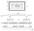
도 2 내지 도 4를 참조하면, 센싱 모드는 구동 모드 전후에 픽셀(P)의 구동 특성을 센싱할 수 있고, 버티컬 블랭크(Vertical blank, VB) 기간 내에서 픽셀(P)의 구동 특성을 센싱할 수 있다. 버티컬 블랭크 기간은 제N(N은 양의 정수) 프레임 기간과 제N+1 프레임 기간 사이에서 데이터 인에이블 신호(Data Enable, DE)가 없는 기간이다. 데이터 인에이블 신호(DE)는 표시패널의 픽셀들(P)에 표시될 입력 영상의 데이터와 동기된다. 버티컬 블랭크 기간에는 입력 영상의 데이터가 입력되지 않는다.2 to 4, the sensing mode may sense driving characteristics of the pixel P before and after the driving mode, and sense driving characteristics of the pixel P within a vertical blank (VB) period. You can. The vertical blank period is a period in which there is no data enable signal (DE) between the Nth (N is a positive integer) frame period and the N + 1th frame period. The data enable signal DE is synchronized with the data of the input image to be displayed on the pixels P of the display panel. During the vertical blank period, data of the input image is not input.
센싱 모드는 제1 및 제3 스위치(S1, S3)를 턴-온(turn-on)시켜 OLED의 애노드를 비교기(111)의 비반전 입력 단자에 연결하고, OLED의 캐소드에 인가되는 저전위 전원 전압(VSS)을 부극성 전압(-V)으로 낮춘다. 센싱 모드에서, 제2 스위치(S2)는 오프(off) 상태를 유지한다.In the sensing mode, the first and third switches S1 and S3 are turned on to connect the anode of the OLED to the non-inverting input terminal of the
구동 모드는 제1 및 제3 스위치(S1, S3)를 턴-오프(turn-off)시키는 반면, 제2 스위치(S2)를 턴-온시켜 OLED의 애노드와 비교기(111) 사이의 전류패스(current path)를 차단하고 OLED의 캐소드에 인가되는 저전위 전원 전압(VSS)을 그라운드 전압(GND)으로 조정한다. 구동 모드에서, 입력 영상의 데이터 전압이 픽셀들(P)에 공급된다.The driving mode turns on and off the first and third switches S1 and S3, while turning on the second switch S2 to pass the current path between the anode of the OLED and the comparator 111 ( current path) and adjust the low potential power voltage (VSS) applied to the cathode of the OLED to the ground voltage (GND). In the driving mode, the data voltage of the input image is supplied to the pixels P.
제1 내지 제3 스위치(S1~S3)의 온/오프 타이밍은 도 9에 도시된 타이밍 콘트롤러(Timing controller, 30)에 의해 제어될 수 있다.The on / off timing of the first to third switches S1 to S3 may be controlled by a
수직 동기 신호(Vsync)의 1 주기는 1 수직 기간으로서 1 프레임 기간의 타이밍을 정의한다. 수평 동기 신호(Hsync)와 데이터 인에이블 신호(DE)의 1 주기는 1 수평기간이다. 데이터 인에이블 신호(DE)의 하이 로직(high logic) 구간 즉, 펄스 폭은 1 라인 데이터 타이밍을 나타낸다. 1 수평 기간은 표시패널(100)에서 1 라인의 픽셀들에 데이터를 기입하는데 필요한 시간(horizontal address time)이다.One period of the vertical synchronization signal Vsync is 1 vertical period and defines the timing of one frame period. One period of the horizontal synchronization signal Hsync and the data enable signal DE is one horizontal period. The high logic section of the data enable signal DE, that is, the pulse width represents one line data timing. One horizontal period is a horizontal address time required to write data to one line of pixels in the
데이터 인에이블 신호(DE)와 입력 영상의 데이터는 데이터 인에이블 기간(AA) 동안 입력되고, 버티컬 블랭크 기간(VB)에 입력되지 않는다. 데이터 인에이블 기간(AA)은 픽셀 어레이의 모든 픽셀들에 1 프레임 분량의 픽셀 데이터를 표시하는데 필요한 시간(Vertical address time)이다.The data enable signal DE and the data of the input image are input during the data enable period AA, and are not input during the vertical blank period VB. The data enable period AA is a time required to display one frame of pixel data for all pixels in the pixel array.
버티컬 블랭크 기간(VB)은 수직 싱크 시간(Vertical sync time, VS), 버티컬 프론트 포치(Vertical Front Porch, FP), 및 버티컬 백 포치(Vertical Back Porch, BP)를 포함한다. 수직 싱크 시간(VS)은 Vsync의 폴링 에지부터 라이징 에지까지의 시간으로서, 한 화면의 시작(또는 끝) 타이밍을 나타낸다.The vertical blank period (VB) includes a vertical sync time (VS), a vertical front porch (FP), and a vertical back porch (Vertical Back Porch, BP). The vertical sync time (VS) is a time from the falling edge to the rising edge of Vsync, and indicates the start (or end) timing of one screen.
버티컬 프론트 포치(FP)는 1 프레임 데이터의 마지막 라인 데이터 타이밍을 나타내는 데이터 인에이블 신호(DE)의 마지막 펄스의 폴링 에지부터 버티컬 블랭크 기간(VB)의 시작까지의 시간이다. 버티컬 백 포치(BP)는 버티컬 블랭크 기간(VB)의 끝부터 1 프레임 데이터의 제1 라인 데이터 타이밍을 나타내는 데이터 인에이블 신호(DE)의 제1 펄스의 라이징 에지까지의 시간이다.The vertical front porch FP is a time from the falling edge of the last pulse of the data enable signal DE indicating the timing of the last line data of one frame data to the start of the vertical blank period VB. The vertical back porch BP is a time from the end of the vertical blank period VB to the rising edge of the first pulse of the data enable signal DE indicating the first line data timing of one frame data.
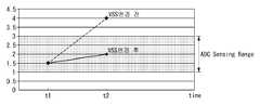
ADC(112)의 센싱 범위가 2V 이고 10 bit 디지털 데이터를 출력하면, 그 ADC는 2V 범위 예를 들어 1~3V를 1024 단계로 나눈 디지털 값으로 변환한다. 비교기(111)의 기준 전압(Vref)이 1V이면, OLED의 애노드 전압이 1V~3V 사이의 전압이 ADC(112)에 입력될 때 픽셀의 구동 특성이 정확하게 센싱될 수 있다. 그런데, 사용 환경이 변하거나 사용 시간이 경과하여 OLED의 애노드 전압이 4V로 상승하면 ADC의 센싱 범위를 넘기 때문에 ADC는 2V에 해당하는 디지털 데이터값 1024를 출력한다. 그 결과, 종래 기술은 OLED의 애노드 전압이 4V일 때 ADC를 통해 센싱된 OLED의 애노드 전압을 2V로 센싱한다. 반면에, 본 발명은 센싱 모드에서 픽셀(P)의 저전위 전원 전압(VSS)을 부극성 전압(-V)으로 낮추어 픽셀의 구동 특성 변화가 ADC의 센싱 범위를 초과하더라도 그 픽셀의 구동 특성 변화를 정확하게 센싱할 수 있다.When the sensing range of the
예를 들어, ADC(112)의 센싱 범위가 2V, 비교기(111)의 기준 전압(Vref)이 1V, OLED의 애노드 전압이 4V 일 때 VSS를 -2.5V로 인가하면 OLED의 애노드 전압은 도 5 및 도 6과 같이 VSS = -2.5V 만큼 낮아져 1.5V로 된다. ADC(112)의 입력 전압이 1.5V 이므로 ADC(112)의 입력 전압이 센싱 범위 내로 조정된다. ADC(112)는 OLED의 애노드 전압 1.5V를 디지털 값으로 출력한다. 옵셋 보상부(113)는 ADC(112)의 출력에 2.5V의 옵셋값을 더한다. 그 결과, 센싱부(110)는 OLED의 애노드 전압이 ADC(112)의 센싱 범위를 초과하더라도 그 OLED의 애노드 전압을 정확하게 센싱할 수 있다.For example, when the sensing range of the
센싱 모드에서, OLED의 애노드 전압 변화를 센싱하고 그 전압 변화와 미리 설정된 초기값을 비교하면, 그 차이를 바탕으로 OLED의 문턱 전압 변화, 구동 TFT의 문턱 전압, TFT의 이동도 변화 등 픽셀(P)의 구동 특성 변화를 추정할 수 있다. 본원 출원인은 OLED의 애노드 전압 변화를 바탕으로 픽셀(P)의 구동 특성 변화를 센싱하는 방법을 대한민국 특허 출원 10-2013-0035184(2013.04.01.), 대한민국 특허 출원 10-2013-0104341(2013.08.30.), 미합중국 특허 출원 14/132783(2013.12.17.) 등에서 제안한 바 있다.In the sensing mode, if the anode voltage change of the OLED is sensed and the voltage change is compared with a preset initial value, pixels (P) such as a change in the threshold voltage of the OLED, a threshold voltage of the driving TFT, and a change in the mobility of the TFT based on the difference ) Can be estimated. Applicant of the present application has applied for a method of sensing a change in driving characteristics of a pixel (P) based on a change in the anode voltage of an OLED. 30.), United
VSS 조정부(100)는 전압 레벨이 다른 다수의 외부 부극성 전압원들을 이용하여 센싱 모드에서 발생되는 부극성 전압(-V)을 픽셀 위치 및/또는 시간에 따라 조정할 수 있다.The
저전위 전원 전압(VSS)은 도 7과 같이 표시패널(10)의 픽셀 위치에 따라 다르게 인가될 수 있다. 예를 들어, 본 발명은 표시패널(10)의 픽셀 어레이를 다수의 블록들로 분할하고 픽셀의 구동 특성 편차를 고려하여 각 블록들 마다 저전위 전원 전압(VSS)을 독립적으로 인가한다.The low potential power voltage VSS may be applied differently according to the pixel position of the
픽셀(P)의 구동 특성 변화는 유기 발광 다이오드 표시장치의 사용 시간이 증가할수록 더 커질 수 있다. 이를 고려하여, 저전위 전원 전압(VSS)은 VSS 조정부(100)에 의해 도 8과 같이 시간이 경과됨에 따라 점차적으로 더 낮은 전압으로 조정될 수 있다. 이 경우, 옵셋 보상부(113)에서 ADC(112)의 출력에 가산될 옵셋 값도 저전위 전원 전압(VSS)의 조정폭 만큼 시간 축 상에서 가변된다.The driving characteristic change of the pixel P may become larger as the use time of the organic light emitting diode display increases. In consideration of this, the low potential power supply voltage VSS may be gradually adjusted to a lower voltage as time elapses as illustrated in FIG. 8 by the
도 9는 본 발명의 실시예에 따른 유기 발광 다이오드 표시장치를 보여 주는 블록도이다.9 is a block diagram showing an organic light emitting diode display according to an exemplary embodiment of the present invention.
도 9를 참조하면, 본 발명의 유기 발광 다이오드 표시장치는 표시패널(10)과, 표시패널 구동회로, 및 전원부(40)를 포함한다.Referring to FIG. 9, the organic light emitting diode display device of the present invention includes a
표시패널(10)의 픽셀 어레이에는 입력 영상의 데이터가 표시된다. 표시패널(10)의 픽셀 어레이는 다수의 데이터 라인들(13)과, 데이터 라인들(13)과 교차되는 다수의 스캔 라인들(15), 및 매트릭스 형태로 배치되는 픽셀들을 포함한다. 픽셀들(P) 각각은 컬러 구현을 위하여 적색 서브 픽셀(R), 녹색 서브 픽셀(G), 및 청색 서브 픽셀(B)로 나뉘어질 수 있다. 또한, 픽셀들(P) 각각은 컬러 구현을 위하여 적색 서브 픽셀(R), 녹색 서브 픽셀(G), 청색 서브 픽셀(B), 및 백색 서브 필터(W)를 나뉘어질 수도 있다.Data of the input image is displayed on the pixel array of the
표시패널 구동회로는 데이터 구동회로(12), 스캔 구동회로(14), 데이터 보상부(20), 센싱부(110) 및 타이밍 콘트롤러(30)를 포함한다. 표시패널 구동회로는 입력 영상의 데이터를 표시패널(10)의 픽셀 어레이에 기입한다. 데이터 보상부(20)는 타이밍 콘트롤러(30) 또는 데이터 구동회로(12)에 내장될 수 있다.The display panel driving circuit includes a
제1 스위치(S1)는 픽셀(P)에 내장될 수 있다. 제2 및 제3 스위치(S2, S3) 밖의 전원부(도 9, 40)에 내장될 수 있다. 비교기(111), ADC(112), 옵셋 보상부(113), 및 DAC(114)는 도 9에 도시된 데이터 구동회로(12)에 내장될 수 있다. 센싱부(110)와 데이터 보상부(20)는 전술한 바 있으므로 그에 대한 상세한 설명을 생략한다.The first switch S1 may be embedded in the pixel P. The second and third switches S2 and S3 may be embedded in the power supply units (FIGS. 9 and 40). The
데이터 구동회로(12)는 DAC(114)를 이용하여 데이터 보상부(20)로부터 입력된 입력 영상의 디지털 비디오 데이터(DATA)를 아날로그 감마보상전압(Vgamma)으로 변환하여 데이터 전압을 발생하고 그 데이터 전압을 데이터 라인들(13)로 출력한다. 데이터 구동회로(12)는 센싱부(110)를 통해 센싱한 픽셀들(P) 각각의 구동 특성 변화를 보상하기 위한 보상값을 타이밍 콘트롤러(30)를 통해 데이터 보상부(20)로 전송할 수 있다.The
스캔 구동회로(14)는 타이밍 콘트롤러(30)의 제어 하에 데이터 인에이블 기간 동안 데이터 구동회로(12)의 출력 전압에 동기되는 스캔 펄스(또는 게이트 펄스)를 스캔 라인들(15)에 공급한다. 스캔 구동회로(14)는 타이밍 콘트롤러(30)의 제어 하에 스위치들(S1~S3)의 제어신호를 발생할 수 있다.The
타이밍 콘트롤러(30)는 도시하지 않은 호스트 시스템(host system)으로부터 입력 영상의 디지털 비디오 데이터(DATA)와, 그와 동기되는 타이밍 신호들을 입력받는다. 타이밍 신호들은 수직 동기신호(Vsync), 수평 동기신호(Hsync), 데이터 인에이블 신호(DE), 도트 클럭(CLK) 등을 포함한다. 타이밍 콘트롤러(30)는 입력 영상의 픽셀 데이터와 함께 수신되는 타이밍 신호들(Vsync, Hsync, DE, DCLK)을 바탕으로 데이터 구동회로(12)와 스캔 구동회로(13)의 동작 타이밍을 제어하기 위한 타이밍 제어신호(DDC, GDC)를 발생한다.The
호스트 시스템은 TV(Television) 시스템, 셋톱박스, 네비게이션 시스템, DVD 플레이어, 블루레이 플레이어, 개인용 컴퓨터(PC), 홈 시어터 시스템, 폰 시스템(Phone system) 중 어느 하나로 구현될 수 있다.The host system may be implemented as any one of a TV (Television) system, a set top box, a navigation system, a DVD player, a Blu-ray player, a personal computer (PC), a home theater system, and a phone system.
전원부(40)는 호스트 시스템으로부터 입력 전압이 공급되면, 픽셀의 고전위 전원 전압(VDD), 저전위 전원 전압(VSS) 및 감마보상전압(Vgamma)을 발생한다. 전원부(40)는 전술한 VSS 조정부(100)를 이용하여 센싱 모드와 구동 모드에서 저전위 전원 전압(VSS)을 변경한다.When the input voltage is supplied from the host system, the
본 발명은 픽셀들 각각의 구동 특성 변화를 정확하게 센싱하여 그 센싱 결과를 바탕으로 픽셀들 각각의 구동 특성 변화를 보상하는 외부 보상 기술을 적용함으로써 유기 발광 다이오드 표시장치의 수율과 수명을 증가시킨다. 또한, 본 발명은 외부 보상 방법을 적용하여 픽셀 내의 내부 보상 회로를 생략하거나 최소화함으로써 픽셀들의 구조를 단순화하여 픽셀의 개구율과 수율을 높일 수 있다.The present invention increases the yield and life of the organic light emitting diode display by applying an external compensation technique that accurately senses the driving characteristic change of each pixel and compensates the driving characteristic change of each pixel based on the sensing result. In addition, the present invention can improve the aperture ratio and yield of the pixel by simplifying the structure of the pixels by omitting or minimizing the internal compensation circuit in the pixel by applying an external compensation method.
이상 설명한 내용을 통해 당업자라면 본 발명의 기술사상을 일탈하지 아니하는 범위에서 다양한 변경 및 수정이 가능함을 알 수 있을 것이다. 따라서, 본 발명의 기술적 범위는 명세서의 상세한 설명에 기재된 내용으로 한정되는 것이 아니라 특허 청구의 범위에 의해 정하여져야만 할 것이다.
Through the above description, those skilled in the art will appreciate that various changes and modifications are possible without departing from the technical idea of the present invention. Therefore, the technical scope of the present invention is not limited to the contents described in the detailed description of the specification, but should be determined by the scope of the claims.
10 : 표시패널12 : 데이터 구동회로
14 : 스캔 구동회로20 : 데이터 보상부
30 : 타이밍 콘트롤러40 : 전원부
100 : VSS 조정부110 : 센싱부
111 : 비교기112 : ADC
114 : DAC10: display panel 12: data driving circuit
14: scan driving circuit 20: data compensation unit
30: timing controller 40: power supply
100: VSS adjustment unit 110: sensing unit
111: comparator 112: ADC
114: DAC
Claims (9)
Translated fromKorean상기 센싱 모드에서 상기 픽셀들의 저전위 전원 전압(VSS)을 부극성 전압으로 낮추고, 상기 구동 모드에서 상기 저전위 전원 전압을 그라운드 전압으로 조정하는 VSS 조정부; 및
아날로그-디지털 변환기(ADC)를 이용하여 상기 센싱 모드에서 상기 유기 발광 다이오드의 애노드 전압을 센싱하는 센싱부를 포함하는 것을 특징으로 하는 유기 발광 다이오드 표시장치.In the organic light emitting diode display device for supplying the data voltage of the input image to the pixels including the organic light emitting diode in the driving mode, and sensing the change in the driving characteristics of the pixels in the sensing mode,
A VSS adjusting unit that lowers the low potential power voltage (VSS) of the pixels to a negative voltage in the sensing mode and adjusts the low potential power voltage to a ground voltage in the driving mode; And
And an sensing unit configured to sense the anode voltage of the organic light emitting diode in the sensing mode using an analog-to-digital converter (ADC).
상기 센싱부로부터 입력된 보상값을 상기 입력 영상의 데이터에 가감하거나 곱하여 상기 픽셀들의 구동 특성 변화를 보상하는 데이터 보상부를 더 포함하는 것을 특징으로 하는 유기 발광 다이오드 표시장치.According to claim 1,
And a data compensation unit that compensates for a change in driving characteristics of the pixels by adding or subtracting the compensation value input from the sensing unit to data of the input image.
상기 센싱부는,
상기 유기 발광 다이오드의 애노드 단자에 연결되고 상기 센싱 모드에서 턴-온되는 제1 스위치;
상기 제1 스위치와 상기 아날로그-디지털 변환기 사이에 연결되어 상기 제1 스위치가 턴-온될 때 상기 유기 발광 다이오드의 애노드 전압과 기준 전압의 차를 상기 아날로그-디지털 변환기로 출력하는 비교기; 및
상기 센싱 모드에서 상기 그라운드 전압과 상기 부극성 전압의 차 만큼 설정된 옵셋값을 상기 아날로그-디지털 변환기의 출력에 더하는 옵셋 보상부를 더 포함하는 것을 특징으로 하는 유기 발광 다이오드 표시장치.According to claim 1,
The sensing unit,
A first switch connected to the anode terminal of the organic light emitting diode and turned on in the sensing mode;
A comparator connected between the first switch and the analog-to-digital converter and outputting a difference between an anode voltage and a reference voltage of the organic light emitting diode to the analog-to-digital converter when the first switch is turned on; And
And an offset compensation unit that adds an offset value set by a difference between the ground voltage and the negative polarity voltage to the output of the analog-to-digital converter in the sensing mode.
상기 VSS 조정부는,
상기 구동 모드에서 상기 유기 발광 다이오드의 캐소드에 상기 그라운드 전압을 공급하는 제2 스위치; 및
상기 센싱 모드에서 상기 유기 발광 다이오드의 캐소드에 상기 부극성 전압을 공급하는 제3 스위치를 더 포함하는 것을 특징으로 하는 유기 발광 다이오드 표시장치.The method of claim 3,
The VSS adjustment unit,
A second switch for supplying the ground voltage to the cathode of the organic light emitting diode in the driving mode; And
And a third switch for supplying the negative voltage to the cathode of the organic light emitting diode in the sensing mode.
상기 VSS 조정부는 상기 센싱 모드에서 인가되는 저전위 전원 전압을 상기 픽셀들의 위치에 따라 다르게 설정하는 것을 특징으로 하는 유기 발광 다이오드 표시장치.According to claim 1,
The VSS adjusting unit sets the low potential power voltage applied in the sensing mode differently according to the position of the pixels.
상기 VSS 조정부는 상기 센싱 모드에서 인가되는 저전위 전원 전압을 시간이 경과됨에 따라 점차 낮추는 것을 특징으로 하는 유기 발광 다이오드 표시장치.The method according to any one of claims 1 to 5,
The VSS adjusting unit gradually lowers the low potential power voltage applied in the sensing mode as time elapses.
상기 센싱 모드에서 상기 픽셀들의 저전위 전원 전압(VSS)을 부극성 전압으로 낮추는 단계;
상기 구동 모드에서 상기 저전위 전원 전압을 그라운드 전압으로 조정하는 단계; 및
아날로그-디지털 변환기(ADC)를 이용하여 상기 센싱 모드에서 상기 유기 발광 다이오드의 애노드 전압을 센싱하는 단계를 포함하는 것을 특징으로 하는 유기 발광 다이오드 표시장치의 구동 특성 센싱 방법.In the driving mode sensing method of supplying a data voltage of an input image to pixels including an organic light emitting diode in the driving mode, and sensing the change in driving characteristics of the pixels in the sensing mode,
Lowering the low potential power voltage (VSS) of the pixels to a negative voltage in the sensing mode;
Adjusting the low potential power voltage to a ground voltage in the driving mode; And
And sensing an anode voltage of the organic light emitting diode in the sensing mode using an analog-to-digital converter (ADC).
상기 센싱 모드에서 상기 픽셀들의 저전위 전원 전압(VSS)을 부극성 전압으로 낮추는 단계는,
상기 센싱 모드에서 인가되는 저전위 전원 전압을 상기 픽셀들의 위치에 따라 다르게 설정하는 것을 특징으로 하는 유기 발광 다이오드 표시장치의 구동 특성 센싱 방법.The method of claim 7,
In the sensing mode, lowering the low potential power voltage (VSS) of the pixels to a negative voltage,
A method of sensing driving characteristics of an organic light emitting diode display, characterized in that a low potential power voltage applied in the sensing mode is set differently according to the positions of the pixels.
상기 센싱 모드에서 상기 픽셀들의 저전위 전원 전압(VSS)을 부극성 전압으로 낮추는 단계;
상기 센싱 모드에서 인가되는 저전위 전원 전압을 시간이 경과됨에 따라 점차 낮추는 것을 특징으로 하는 유기 발광 다이오드 표시장치의 구동 특성 센싱 방법.The method of claim 7 or 8,
Lowering the low potential power voltage (VSS) of the pixels to a negative voltage in the sensing mode;
A method of sensing driving characteristics of an organic light emitting diode display, characterized in that the low potential power voltage applied in the sensing mode is gradually lowered over time.
Priority Applications (3)
| Application Number | Priority Date | Filing Date | Title |
|---|---|---|---|
| KR1020130164614AKR102103241B1 (en) | 2013-12-26 | 2013-12-26 | Organic light emitting diode display device and method of sensing driving characteristics thereof |
| US14/565,138US9607553B2 (en) | 2013-12-26 | 2014-12-09 | Organic light emitting diode display and method for sensing driving characteristics thereof |
| CN201410858134.7ACN104751793B (en) | 2013-12-26 | 2014-12-24 | Organic light emitting diode display and the method for sensing its drive characteristic |
Applications Claiming Priority (1)
| Application Number | Priority Date | Filing Date | Title |
|---|---|---|---|
| KR1020130164614AKR102103241B1 (en) | 2013-12-26 | 2013-12-26 | Organic light emitting diode display device and method of sensing driving characteristics thereof |
Publications (2)
| Publication Number | Publication Date |
|---|---|
| KR20150076028A KR20150076028A (en) | 2015-07-06 |
| KR102103241B1true KR102103241B1 (en) | 2020-04-22 |
Family
ID=53482473
Family Applications (1)
| Application Number | Title | Priority Date | Filing Date |
|---|---|---|---|
| KR1020130164614AActiveKR102103241B1 (en) | 2013-12-26 | 2013-12-26 | Organic light emitting diode display device and method of sensing driving characteristics thereof |
Country Status (3)
| Country | Link |
|---|---|
| US (1) | US9607553B2 (en) |
| KR (1) | KR102103241B1 (en) |
| CN (1) | CN104751793B (en) |
Families Citing this family (43)
| Publication number | Priority date | Publication date | Assignee | Title |
|---|---|---|---|---|
| KR102192522B1 (en)* | 2014-08-06 | 2020-12-18 | 엘지디스플레이 주식회사 | Organic light emitting display device |
| CN105280140B (en)* | 2015-11-24 | 2018-02-16 | 深圳市华星光电技术有限公司 | Sensing circuit and corresponding OLED display devices |
| KR102496782B1 (en) | 2015-12-31 | 2023-02-08 | 엘지디스플레이 주식회사 | Voltage conversion circuit and organic lighting emitting device having the saeme |
| CN105427792A (en)* | 2016-01-05 | 2016-03-23 | 京东方科技集团股份有限公司 | Pixel compensation circuit and driving method thereof, display panel, and display apparatus |
| KR102575122B1 (en)* | 2016-01-20 | 2023-09-06 | 주식회사 엘엑스세미콘 | Source driver |
| KR102586459B1 (en)* | 2016-01-20 | 2023-10-10 | 주식회사 엘엑스세미콘 | Source driver for display apparatus |
| US10540924B2 (en) | 2016-01-20 | 2020-01-21 | Silicon Works Co., Ltd | Source driver |
| CN105513541B (en)* | 2016-02-25 | 2018-11-23 | 深圳市华星光电技术有限公司 | The data compensating circuit and method and OLED display of OLED |
| CN105609029B (en) | 2016-03-24 | 2019-10-01 | 深圳市华星光电技术有限公司 | Sense the system and AMOLED display device of AMOLED pixel driver characteristic |
| US10096284B2 (en)* | 2016-06-30 | 2018-10-09 | Apple Inc. | System and method for external pixel compensation |
| KR102520025B1 (en)* | 2016-06-30 | 2023-04-11 | 엘지디스플레이 주식회사 | Organic light emitting display device, base voltage control circuit and power management integrated circuit |
| KR102474753B1 (en)* | 2016-09-05 | 2022-12-07 | 엘지디스플레이 주식회사 | Organic light emitting display panel, organic light emitting display device and driving method |
| KR102526355B1 (en)* | 2016-09-22 | 2023-05-02 | 엘지디스플레이 주식회사 | Organic Light Emitting Display Device |
| KR102460534B1 (en)* | 2016-09-30 | 2022-11-01 | 엘지디스플레이 주식회사 | Organic light emitting display module, organic light emitting display device, and base voltage control system |
| CN106328061B (en)* | 2016-10-14 | 2019-03-12 | 深圳市华星光电技术有限公司 | OLED pixel mixed compensation circuit and mixed compensation method |
| KR102627275B1 (en)* | 2016-10-25 | 2024-01-23 | 엘지디스플레이 주식회사 | Organic Light Emitting Display Device |
| KR102648975B1 (en) | 2016-11-30 | 2024-03-19 | 엘지디스플레이 주식회사 | Organic Light Emitting Display and Compensation Method of Driving Characteristic thereof |
| KR102587318B1 (en) | 2016-12-05 | 2023-10-12 | 티씨엘 차이나 스타 옵토일렉트로닉스 테크놀로지 컴퍼니 리미티드 | Gate driving circuit and display device having the same |
| KR102645205B1 (en)* | 2016-12-13 | 2024-03-07 | 주식회사 엘엑스세미콘 | Pixel sensing apparatus and panel driving apparatus |
| KR102630608B1 (en)* | 2016-12-21 | 2024-01-26 | 엘지디스플레이 주식회사 | Organic light emitting display device and method for driving the same |
| KR102565753B1 (en)* | 2016-12-28 | 2023-08-11 | 엘지디스플레이 주식회사 | Electroluminescent Display Device and Driving Device thereof |
| CN106652911B (en) | 2017-02-24 | 2019-03-12 | 深圳市华星光电半导体显示技术有限公司 | OLED pixel driving circuit and OLED display |
| CN106935193A (en)* | 2017-05-12 | 2017-07-07 | 京东方科技集团股份有限公司 | OLED drives compensation circuit, OLED display panel and its driving method |
| KR102381286B1 (en) | 2017-05-18 | 2022-03-31 | 삼성디스플레이 주식회사 | Display device |
| CN107068049B (en)* | 2017-06-07 | 2020-05-29 | 京东方科技集团股份有限公司 | Image display driving device, display device and electrical compensation method |
| KR102439001B1 (en) | 2017-07-31 | 2022-08-31 | 엘지디스플레이 주식회사 | organic light emitting diode display |
| KR102379777B1 (en)* | 2017-08-23 | 2022-03-28 | 엘지디스플레이 주식회사 | Electroluminescent System And How To Set Reference Voltage Of The Same |
| CN107424560B (en)* | 2017-08-24 | 2020-03-13 | 京东方科技集团股份有限公司 | Method and device for detecting threshold voltage of driving transistor in display panel |
| CN108154847A (en)* | 2018-01-19 | 2018-06-12 | 昆山国显光电有限公司 | The driving device and driving method of organic light emitting display |
| TWI649741B (en)* | 2018-01-30 | 2019-02-01 | 友達光電股份有限公司 | Threshold voltage compensation circuit and display panel |
| KR102507622B1 (en)* | 2018-07-25 | 2023-03-07 | 엘지디스플레이 주식회사 | Light emitting display device |
| TWI676979B (en)* | 2018-11-20 | 2019-11-11 | 友達光電股份有限公司 | Display panel and testing method of display panel |
| CN109545139B (en)* | 2018-12-13 | 2020-06-05 | 昆山国显光电有限公司 | Pixel compensation circuit, method and display device |
| CN110415644B (en)* | 2019-08-02 | 2023-06-30 | 京东方科技集团股份有限公司 | Pixel driving circuit and method thereof, and display panel |
| KR102676645B1 (en)* | 2019-10-10 | 2024-06-21 | 삼성디스플레이 주식회사 | Display device |
| CN110718190A (en)* | 2019-11-15 | 2020-01-21 | Oppo广东移动通信有限公司 | Voltage adjustment method, pixel circuit, and electronic device |
| CN111583864B (en)* | 2020-06-11 | 2021-09-03 | 京东方科技集团股份有限公司 | Display driving circuit, driving method thereof and display device |
| KR102810624B1 (en)* | 2021-02-23 | 2025-05-22 | 삼성디스플레이 주식회사 | Pixel circuit, display apparatus including the same and method of driving the same |
| KR102773743B1 (en)* | 2021-12-13 | 2025-02-27 | 엘지디스플레이 주식회사 | Electroluminescence Display Device And Method For Detecting Display Defect Of The Same |
| KR20240077539A (en)* | 2022-11-22 | 2024-06-03 | 삼성디스플레이 주식회사 | Display device |
| US12340737B2 (en)* | 2022-12-16 | 2025-06-24 | Apple Inc. | Global nonlinear scaler for multiple pixel gamma response compensation |
| CN117095646B (en)* | 2023-09-13 | 2025-04-08 | 格兰菲智能科技股份有限公司 | Compensation circuit, display driver chip, display panel and driving method thereof |
| KR20250060677A (en)* | 2023-10-26 | 2025-05-07 | 엘지디스플레이 주식회사 | Light emitting display panel and light emitting display apparatus using the same |
Family Cites Families (14)
| Publication number | Priority date | Publication date | Assignee | Title |
|---|---|---|---|---|
| JP4612452B2 (en) | 2005-03-30 | 2011-01-12 | Necディスプレイソリューションズ株式会社 | Liquid crystal display device |
| KR101416904B1 (en) | 2007-11-07 | 2014-07-09 | 엘지디스플레이 주식회사 | Driving apparatus for organic electro-luminescence display device |
| KR101634286B1 (en)* | 2009-01-23 | 2016-07-11 | 삼성디스플레이 주식회사 | Display device and driving method thereof |
| KR101084236B1 (en) | 2010-05-12 | 2011-11-16 | 삼성모바일디스플레이주식회사 | Display device and driving method |
| KR101749751B1 (en)* | 2010-10-21 | 2017-06-22 | 엘지디스플레이 주식회사 | Scan pulse switching circuit and display device using the same |
| KR102040843B1 (en)* | 2011-01-04 | 2019-11-06 | 삼성디스플레이 주식회사 | Organic light emitting display and driving method thereof |
| KR101908513B1 (en)* | 2011-08-30 | 2018-10-17 | 엘지디스플레이 주식회사 | Organic light emitting diode display device for sensing pixel current and method for sensing pixel current thereof |
| US9236011B2 (en)* | 2011-08-30 | 2016-01-12 | Lg Display Co., Ltd. | Organic light emitting diode display device for pixel current sensing in the sensing mode and pixel current sensing method thereof |
| KR101350592B1 (en)* | 2011-12-12 | 2014-01-16 | 엘지디스플레이 주식회사 | Organic light-emitting display device |
| KR101356968B1 (en)* | 2012-06-14 | 2014-02-03 | 엘지디스플레이 주식회사 | Display device with integrated touch screen |
| KR20130140445A (en)* | 2012-06-14 | 2013-12-24 | 삼성디스플레이 주식회사 | Display device, power control device and driving method thereof |
| KR101978780B1 (en) | 2013-04-01 | 2019-05-16 | 엘지디스플레이 주식회사 | Image Quality Compensation Device And Method Of Organic Light Emitting Display |
| CN203311812U (en) | 2013-05-30 | 2013-11-27 | 京东方科技集团股份有限公司 | Touch display drive circuit and display device |
| KR102014852B1 (en) | 2013-08-30 | 2019-08-27 | 엘지디스플레이 주식회사 | Image Quality Compensation Device And Method Of Organic Light Emitting Display |
- 2013
- 2013-12-26KRKR1020130164614Apatent/KR102103241B1/enactiveActive
- 2014
- 2014-12-09USUS14/565,138patent/US9607553B2/enactiveActive
- 2014-12-24CNCN201410858134.7Apatent/CN104751793B/enactiveActive
Also Published As
| Publication number | Publication date |
|---|---|
| CN104751793A (en) | 2015-07-01 |
| US9607553B2 (en) | 2017-03-28 |
| KR20150076028A (en) | 2015-07-06 |
| US20150187278A1 (en) | 2015-07-02 |
| CN104751793B (en) | 2017-06-06 |
Similar Documents
| Publication | Publication Date | Title |
|---|---|---|
| KR102103241B1 (en) | Organic light emitting diode display device and method of sensing driving characteristics thereof | |
| US10475386B2 (en) | Display panel and electroluminescence display using the same | |
| US10032405B2 (en) | Organic light-emitting display and method for driving the same | |
| CN104715720B (en) | Organic light emitting diode display | |
| KR102450894B1 (en) | Electroluminescent Display Device And Driving Method Of The Same | |
| KR102401355B1 (en) | Electroluminescence display and driving method thereof | |
| KR20210017876A (en) | Display device and driving method thereof | |
| EP3038091A2 (en) | Organic light emitting diode display and method for sensing characteristic thereof | |
| US11653538B2 (en) | Pixel array substrate and display device including AC EVEDD driver and display device including the same | |
| KR20150012022A (en) | Organic light emitting display device and driving method thereof | |
| KR102475072B1 (en) | Electroluminescence display and driving method thereof | |
| KR102603538B1 (en) | Display device and driving method thereof | |
| KR20190074847A (en) | Image Quality Compensation Device And Method Of Display Device | |
| KR20210007508A (en) | Display device and driving method thereof | |
| KR102296403B1 (en) | Electroluminescence display and driving method thereof | |
| KR102379777B1 (en) | Electroluminescent System And How To Set Reference Voltage Of The Same | |
| KR20210082602A (en) | Pixel circuit, electroluminescent display using the same, and method for sensing chracteristic of light emission control transistor using the same | |
| KR102494924B1 (en) | Organic Light Emitting Display Device And Driving Method Thereof | |
| KR102676123B1 (en) | Display device and driving method thereof | |
| KR102544502B1 (en) | Pixel sensing device and electroluminescence display using the same | |
| KR102417423B1 (en) | Electroluminescence display and driving method thereof | |
| KR20210085089A (en) | Pixel circuit and electroluminescent display using the same | |
| KR102478991B1 (en) | Electroluminescence display and driving method thereof | |
| KR102390477B1 (en) | Organic Light Emitting Diode display device and method for driving the same | |
| KR20240119407A (en) | Sensing circuit and display device including the same |
Legal Events
| Date | Code | Title | Description |
|---|---|---|---|
| PA0109 | Patent application | Patent event code:PA01091R01D Comment text:Patent Application Patent event date:20131226 | |
| PG1501 | Laying open of application | ||
| A201 | Request for examination | ||
| PA0201 | Request for examination | Patent event code:PA02012R01D Patent event date:20181203 Comment text:Request for Examination of Application Patent event code:PA02011R01I Patent event date:20131226 Comment text:Patent Application | |
| E902 | Notification of reason for refusal | ||
| PE0902 | Notice of grounds for rejection | Comment text:Notification of reason for refusal Patent event date:20191125 Patent event code:PE09021S01D | |
| E701 | Decision to grant or registration of patent right | ||
| PE0701 | Decision of registration | Patent event code:PE07011S01D Comment text:Decision to Grant Registration Patent event date:20200129 | |
| GRNT | Written decision to grant | ||
| PR0701 | Registration of establishment | Comment text:Registration of Establishment Patent event date:20200416 Patent event code:PR07011E01D | |
| PR1002 | Payment of registration fee | Payment date:20200417 End annual number:3 Start annual number:1 | |
| PG1601 | Publication of registration | ||
| PR1001 | Payment of annual fee | Payment date:20240315 Start annual number:5 End annual number:5 | |
| PR1001 | Payment of annual fee | Payment date:20250318 Start annual number:6 End annual number:6 |