KR102103196B1 - Multilayer electronics assembly and method for embedding electrical circuit components within a three dimensional module - Google Patents
Multilayer electronics assembly and method for embedding electrical circuit components within a three dimensional moduleDownload PDFInfo
- Publication number
- KR102103196B1 KR102103196B1KR1020147024985AKR20147024985AKR102103196B1KR 102103196 B1KR102103196 B1KR 102103196B1KR 1020147024985 AKR1020147024985 AKR 1020147024985AKR 20147024985 AKR20147024985 AKR 20147024985AKR 102103196 B1KR102103196 B1KR 102103196B1
- Authority
- KR
- South Korea
- Prior art keywords
- electrical circuit
- circuit component
- substrate
- bonding material
- temperature
- Prior art date
- Legal status (The legal status is an assumption and is not a legal conclusion. Google has not performed a legal analysis and makes no representation as to the accuracy of the status listed.)
- Active
Links
- 238000000034methodMethods0.000titleclaimsdescription80
- 239000000758substrateSubstances0.000claimsabstractdescription149
- 239000000463materialSubstances0.000claimsabstractdescription118
- 230000004927fusionEffects0.000claimsabstractdescription63
- 230000007704transitionEffects0.000claimsdescription34
- BQCADISMDOOEFD-UHFFFAOYSA-NSilverChemical compound[Ag]BQCADISMDOOEFD-UHFFFAOYSA-N0.000claimsdescription33
- 239000004065semiconductorSubstances0.000claimsdescription24
- 229910000679solderInorganic materials0.000claimsdescription21
- 239000002131composite materialSubstances0.000claimsdescription16
- 239000007788liquidSubstances0.000claimsdescription15
- 238000002844meltingMethods0.000claimsdescription14
- 230000008018meltingEffects0.000claimsdescription13
- 239000003990capacitorSubstances0.000claimsdescription11
- 229920002313fluoropolymerPolymers0.000claimsdescription10
- 239000004811fluoropolymerSubstances0.000claimsdescription10
- 229910045601alloyInorganic materials0.000claimsdescription9
- 239000000956alloySubstances0.000claimsdescription9
- 239000007787solidSubstances0.000claimsdescription7
- 230000009969flowable effectEffects0.000claimsdescription5
- 238000000429assemblyMethods0.000abstractdescription4
- 230000000712assemblyEffects0.000abstractdescription3
- 238000004519manufacturing processMethods0.000abstractdescription3
- 238000005245sinteringMethods0.000description18
- RYGMFSIKBFXOCR-UHFFFAOYSA-NCopperChemical compound[Cu]RYGMFSIKBFXOCR-UHFFFAOYSA-N0.000description14
- 229910052802copperInorganic materials0.000description14
- 239000010949copperSubstances0.000description14
- 229920001343polytetrafluoroethylenePolymers0.000description12
- 239000004810polytetrafluoroethyleneSubstances0.000description12
- 239000007791liquid phaseSubstances0.000description9
- 239000010408filmSubstances0.000description6
- 238000005516engineering processMethods0.000description5
- 239000012071phaseSubstances0.000description5
- 238000012805post-processingMethods0.000description5
- 239000004593EpoxySubstances0.000description4
- 238000005530etchingMethods0.000description4
- 238000012545processingMethods0.000description4
- 238000007796conventional methodMethods0.000description3
- 238000005520cutting processMethods0.000description3
- 239000003365glass fiberSubstances0.000description3
- -1polytetrafluoroethylenePolymers0.000description3
- 239000010409thin filmSubstances0.000description3
- 230000001052transient effectEffects0.000description3
- PIGFYZPCRLYGLF-UHFFFAOYSA-NAluminum nitrideChemical compound[Al]#NPIGFYZPCRLYGLF-UHFFFAOYSA-N0.000description2
- 239000004952PolyamideSubstances0.000description2
- 239000011230binding agentSubstances0.000description2
- 239000000919ceramicSubstances0.000description2
- 238000005553drillingMethods0.000description2
- 239000000835fiberSubstances0.000description2
- 239000011521glassSubstances0.000description2
- 239000011159matrix materialSubstances0.000description2
- 229910000159nickel phosphateInorganic materials0.000description2
- CLDVQCMGOSGNIW-UHFFFAOYSA-Nnickel tinChemical compound[Ni].[Sn]CLDVQCMGOSGNIW-UHFFFAOYSA-N0.000description2
- JOCJYBPHESYFOK-UHFFFAOYSA-Knickel(3+);phosphateChemical compound[Ni+3].[O-]P([O-])([O-])=OJOCJYBPHESYFOK-UHFFFAOYSA-K0.000description2
- 238000004806packaging method and processMethods0.000description2
- 238000007747platingMethods0.000description2
- 229920002647polyamidePolymers0.000description2
- 229920000642polymerPolymers0.000description2
- 239000011347resinSubstances0.000description2
- 229920005989resinPolymers0.000description2
- 238000005476solderingMethods0.000description2
- 239000002904solventSubstances0.000description2
- 229910000962AlSiCInorganic materials0.000description1
- 239000000853adhesiveSubstances0.000description1
- 230000001070adhesive effectEffects0.000description1
- 238000005266castingMethods0.000description1
- 238000001816coolingMethods0.000description1
- 239000003989dielectric materialSubstances0.000description1
- 239000008393encapsulating agentSubstances0.000description1
- 239000011152fibreglassSubstances0.000description1
- 230000005669field effectEffects0.000description1
- 238000007499fusion processingMethods0.000description1
- 230000009477glass transitionEffects0.000description1
- 239000002241glass-ceramicSubstances0.000description1
- PCHJSUWPFVWCPO-UHFFFAOYSA-NgoldChemical compound[Au]PCHJSUWPFVWCPO-UHFFFAOYSA-N0.000description1
- 229910052737goldInorganic materials0.000description1
- 239000010931goldSubstances0.000description1
- 238000010438heat treatmentMethods0.000description1
- 230000036039immunityEffects0.000description1
- 238000010348incorporationMethods0.000description1
- 229910044991metal oxideInorganic materials0.000description1
- 150000004706metal oxidesChemical class0.000description1
- 238000010943off-gassingMethods0.000description1
- 230000003071parasitic effectEffects0.000description1
- 239000002245particleSubstances0.000description1
- 238000002360preparation methodMethods0.000description1
- 230000002787reinforcementEffects0.000description1
- 238000007650screen-printingMethods0.000description1
- 229910052709silverInorganic materials0.000description1
- 239000004332silverSubstances0.000description1
- 125000006850spacer groupChemical group0.000description1
- 238000005382thermal cyclingMethods0.000description1
- XLYOFNOQVPJJNP-UHFFFAOYSA-NwaterSubstancesOXLYOFNOQVPJJNP-UHFFFAOYSA-N0.000description1
Images


Classifications
- H—ELECTRICITY
- H05—ELECTRIC TECHNIQUES NOT OTHERWISE PROVIDED FOR
- H05K—PRINTED CIRCUITS; CASINGS OR CONSTRUCTIONAL DETAILS OF ELECTRIC APPARATUS; MANUFACTURE OF ASSEMBLAGES OF ELECTRICAL COMPONENTS
- H05K1/00—Printed circuits
- H05K1/02—Details
- H05K1/0296—Conductive pattern lay-out details not covered by sub groups H05K1/02 - H05K1/0295
- H05K1/0298—Multilayer circuits
- H—ELECTRICITY
- H05—ELECTRIC TECHNIQUES NOT OTHERWISE PROVIDED FOR
- H05K—PRINTED CIRCUITS; CASINGS OR CONSTRUCTIONAL DETAILS OF ELECTRIC APPARATUS; MANUFACTURE OF ASSEMBLAGES OF ELECTRICAL COMPONENTS
- H05K1/00—Printed circuits
- H05K1/18—Printed circuits structurally associated with non-printed electric components
- H05K1/182—Printed circuits structurally associated with non-printed electric components associated with components mounted in the printed circuit board, e.g. insert mounted components [IMC]
- H05K1/185—Components encapsulated in the insulating substrate of the printed circuit or incorporated in internal layers of a multilayer circuit
- H05K1/186—Components encapsulated in the insulating substrate of the printed circuit or incorporated in internal layers of a multilayer circuit manufactured by mounting on or connecting to patterned circuits before or during embedding
- H—ELECTRICITY
- H05—ELECTRIC TECHNIQUES NOT OTHERWISE PROVIDED FOR
- H05K—PRINTED CIRCUITS; CASINGS OR CONSTRUCTIONAL DETAILS OF ELECTRIC APPARATUS; MANUFACTURE OF ASSEMBLAGES OF ELECTRICAL COMPONENTS
- H05K13/00—Apparatus or processes specially adapted for manufacturing or adjusting assemblages of electric components
- H05K13/04—Mounting of components, e.g. of leadless components
- H05K13/046—Surface mounting
- H05K13/0465—Surface mounting by soldering
- H—ELECTRICITY
- H01—ELECTRIC ELEMENTS
- H01L—SEMICONDUCTOR DEVICES NOT COVERED BY CLASS H10
- H01L2224/00—Indexing scheme for arrangements for connecting or disconnecting semiconductor or solid-state bodies and methods related thereto as covered by H01L24/00
- H01L2224/01—Means for bonding being attached to, or being formed on, the surface to be connected, e.g. chip-to-package, die-attach, "first-level" interconnects; Manufacturing methods related thereto
- H01L2224/26—Layer connectors, e.g. plate connectors, solder or adhesive layers; Manufacturing methods related thereto
- H01L2224/31—Structure, shape, material or disposition of the layer connectors after the connecting process
- H01L2224/32—Structure, shape, material or disposition of the layer connectors after the connecting process of an individual layer connector
- H01L2224/321—Disposition
- H01L2224/32151—Disposition the layer connector connecting between a semiconductor or solid-state body and an item not being a semiconductor or solid-state body, e.g. chip-to-substrate, chip-to-passive
- H01L2224/32221—Disposition the layer connector connecting between a semiconductor or solid-state body and an item not being a semiconductor or solid-state body, e.g. chip-to-substrate, chip-to-passive the body and the item being stacked
- H01L2224/32225—Disposition the layer connector connecting between a semiconductor or solid-state body and an item not being a semiconductor or solid-state body, e.g. chip-to-substrate, chip-to-passive the body and the item being stacked the item being non-metallic, e.g. insulating substrate with or without metallisation
- H—ELECTRICITY
- H01—ELECTRIC ELEMENTS
- H01L—SEMICONDUCTOR DEVICES NOT COVERED BY CLASS H10
- H01L2224/00—Indexing scheme for arrangements for connecting or disconnecting semiconductor or solid-state bodies and methods related thereto as covered by H01L24/00
- H01L2224/80—Methods for connecting semiconductor or other solid state bodies using means for bonding being attached to, or being formed on, the surface to be connected
- H01L2224/83—Methods for connecting semiconductor or other solid state bodies using means for bonding being attached to, or being formed on, the surface to be connected using a layer connector
- H01L2224/832—Applying energy for connecting
- H01L2224/83201—Compression bonding
- H01L2224/83203—Thermocompression bonding, e.g. diffusion bonding, pressure joining, thermocompression welding or solid-state welding
- H01L2224/83204—Thermocompression bonding, e.g. diffusion bonding, pressure joining, thermocompression welding or solid-state welding with a graded temperature profile
- H—ELECTRICITY
- H01—ELECTRIC ELEMENTS
- H01L—SEMICONDUCTOR DEVICES NOT COVERED BY CLASS H10
- H01L2224/00—Indexing scheme for arrangements for connecting or disconnecting semiconductor or solid-state bodies and methods related thereto as covered by H01L24/00
- H01L2224/80—Methods for connecting semiconductor or other solid state bodies using means for bonding being attached to, or being formed on, the surface to be connected
- H01L2224/83—Methods for connecting semiconductor or other solid state bodies using means for bonding being attached to, or being formed on, the surface to be connected using a layer connector
- H01L2224/832—Applying energy for connecting
- H01L2224/8321—Applying energy for connecting using a reflow oven
- H01L2224/83211—Applying energy for connecting using a reflow oven with a graded temperature profile
- H—ELECTRICITY
- H01—ELECTRIC ELEMENTS
- H01L—SEMICONDUCTOR DEVICES NOT COVERED BY CLASS H10
- H01L2224/00—Indexing scheme for arrangements for connecting or disconnecting semiconductor or solid-state bodies and methods related thereto as covered by H01L24/00
- H01L2224/80—Methods for connecting semiconductor or other solid state bodies using means for bonding being attached to, or being formed on, the surface to be connected
- H01L2224/83—Methods for connecting semiconductor or other solid state bodies using means for bonding being attached to, or being formed on, the surface to be connected using a layer connector
- H01L2224/838—Bonding techniques
- H01L2224/8384—Sintering
- H—ELECTRICITY
- H01—ELECTRIC ELEMENTS
- H01L—SEMICONDUCTOR DEVICES NOT COVERED BY CLASS H10
- H01L2924/00—Indexing scheme for arrangements or methods for connecting or disconnecting semiconductor or solid-state bodies as covered by H01L24/00
- H01L2924/10—Details of semiconductor or other solid state devices to be connected
- H01L2924/11—Device type
- H01L2924/13—Discrete devices, e.g. 3 terminal devices
- H01L2924/1304—Transistor
- H01L2924/1306—Field-effect transistor [FET]
- H01L2924/13091—Metal-Oxide-Semiconductor Field-Effect Transistor [MOSFET]
- H—ELECTRICITY
- H05—ELECTRIC TECHNIQUES NOT OTHERWISE PROVIDED FOR
- H05K—PRINTED CIRCUITS; CASINGS OR CONSTRUCTIONAL DETAILS OF ELECTRIC APPARATUS; MANUFACTURE OF ASSEMBLAGES OF ELECTRICAL COMPONENTS
- H05K3/00—Apparatus or processes for manufacturing printed circuits
- H05K3/46—Manufacturing multilayer circuits
- H05K3/4611—Manufacturing multilayer circuits by laminating two or more circuit boards
- H05K3/4623—Manufacturing multilayer circuits by laminating two or more circuit boards the circuit boards having internal via connections between two or more circuit layers before lamination, e.g. double-sided circuit boards
Landscapes
- Engineering & Computer Science (AREA)
- Microelectronics & Electronic Packaging (AREA)
- Manufacturing & Machinery (AREA)
- Production Of Multi-Layered Print Wiring Board (AREA)
- Combinations Of Printed Boards (AREA)
Abstract
Translated fromKorean
Description
Translated fromKorean본 발명은 다층 전자기기 어셈블리 및 관련된 제조 방법에 관한 것이다.The present invention relates to a multilayer electronics assembly and related manufacturing method.
통상적으로, 에폭시 유리섬유(FR4), (폴리테트라플루오로에틸렌, PTFE 같은) 플루오로폴리머 복합체 또는 혼합 유전체(MDk, FR4와 PTFE의 조합)를 이용하는 다층 인쇄 회로 기판들은 다층 구조의 표면 상에 장착되는 부품들에 신호들을 보내도록 사용되었다. 이러한 다층 인쇄 회로 보드들은 가장 일반적으로 부품들에 신호들을 보내기 위한 하나의 수단으로서 에칭된 구리인 트레이스들을 포함한다. 이러한 회로들에서, 레지스터들은 스크린-인쇄되거나 에칭될 수 있다. 이러한 다층 인쇄 회로 보드 어셈블리들은 특히 RF 및 전력 전자기기 모듈들을 포함하는 다양한 적용들에서 사용될 수 있다. 일 예시로서, 이러한 기술들은 그것들의 표면 상에 모놀리식 마이크로파가 통합된 회로들(monolithic microwave integrated circuits; MMICs)을 가지는 다기능 모듈들(MFM)을 형성할 수 있다.Typically, multilayer printed circuit boards using epoxy glass fibers (FR4), fluoropolymer composites (such as polytetrafluoroethylene, PTFE) or mixed dielectrics (combinations of MDk, FR4 and PTFE) are mounted on the surface of a multilayer structure. It was used to send signals to the components. These multilayer printed circuit boards most commonly include traces that are etched copper as a means to send signals to the components. In these circuits, the resistors can be screen-printed or etched. These multilayer printed circuit board assemblies can be used in a variety of applications, particularly including RF and power electronics modules. As an example, these techniques can form multifunctional modules (MFMs) with monolithic microwave integrated circuits (MMICs) on their surface.
다른 종래의 방법에서, 다층 통합된 회로 및 마이크로파, 다기능 모듈들은 퓨전 접합 프로세스를 활용하여 다층 구조로 함께 접합되는 플루오로폴리머 복합체 기판들의 다층으로 구조된다. 복합체 기판 물질은 유리섬유 및 세라믹으로 채워진 PTFE일 수 있다. 이러한 다층 구조들은 퓨전 프로세스 전에 개별적인 층들 안에 에칭되거나 스크린 인쇄되는 얇은 필름 레지스터들을 포함할 수 있다. 예를 들어, 레지스터들은 구리 에칭과 유사한 방법으로, 구리 층들에 인접한 얇은 니켈 인산염 필름들 안에 에칭될 수 있다.In another conventional method, multi-layer integrated circuits and microwave, multi-functional modules are constructed of multiple layers of fluoropolymer composite substrates bonded together in a multi-layer structure utilizing a fusion bonding process. The composite substrate material may be PTFE filled with glass fiber and ceramic. These multilayer structures may include thin film resistors that are etched or screen printed into individual layers prior to the fusion process. For example, resistors can be etched into thin nickel phosphate films adjacent copper layers, in a similar way to copper etching.
특정한 별개의 전기 회로 부품들, 예를 들어, 수동 별개의 레지스터들, 캐패시터들, 자기 디바이스들 및 능동 반도체 디바이스들 같이 별개의 디바이스들은, 단지 에칭 또는 스크린 프린팅으로 생성된 얇은 필름들인 것은 아니다. 사실, 이러한 별개의 디바이스들은 퓨전 접합 프로세스의 열 및/또는 압력을 견딜 수 없는 예를 들어 솔더 페이스트로 기판에 부착된다. 다층 통합된 어셈블리 안으로 별개의 전기 회로 부품들을 포함시키기 위해, 종래의 방법은 개별적인 기판 층들 안에 캐비티들을 형성하는 단계, 캐비티들 내에 별개의 전기 회로 부품들을 부착하는 단계 및 분리된, 포스트-퓨전 접합 단계로서 폴리머 접합 필름 층을 적용하는 단계를 포함한다. 예를 들어, Logothetis 외에 의한 미국 특허 No. 6,009,677와 McAndrews 외에 의한 미국 특허 No. 6,395,374는 퓨전 접합된 플루오로폴리머 복합체 기판들의 다층 구조를 제작하기 위한 프로세스를 설명하고 별개의 전기 회로 부품들은 다층 구조 내에 형성된 캐비티들 안에 접합 후에(post-bonding) 부착되고, 그런 다음 필름이 접합된 층으로 덮인다.Distinct devices, such as certain discrete electrical circuit components, for example passive discrete resistors, capacitors, magnetic devices and active semiconductor devices, are not just thin films produced by etching or screen printing. In fact, these separate devices are attached to the substrate with, for example, a solder paste that cannot withstand the heat and / or pressure of the fusion bonding process. To include discrete electrical circuit components into a multi-layer integrated assembly, conventional methods include forming cavities in separate substrate layers, attaching separate electrical circuit components within the cavities, and separate, post-fusion bonding steps. As applying a layer of a polymer bonding film. For example, US Patent No. by Logothetis et al. US Patent No. 6,009,677 and McAndrews et al. 6,395,374 describe a process for fabricating a multilayer structure of fusion bonded fluoropolymer composite substrates and separate electrical circuit components are attached post-bonding into cavities formed in the multilayer structure, and then the film is bonded Covered with layers.
다층 전자기기 어셈블리는 다음과 같은 별개의 부품들을 부착하기 위한 접합 물질을 이용하여 달성될 수 있다는 것을 발견했다: (1) 별개의 부품들이 부착되는 다층 구조의 층들의 글래스 전이 온도(glass transition temperature)보다 낮은 별개의 부품들을 부착하기 위한 프로세싱 온도(processing temperature)를 구비하고, (2) 액체, 흐를 수 있는, 또는 유연한 상태로 다시 변화하기 위해 상당히 더 높은 온도의 포스트-프로세싱을 요구하게 되는 별개의 부품들을 부착하기 위해 프로세싱 다음에 상 전이를 겪게 되고, 포스트-프로세싱(post-processing) 상 전이 온도는 또한 다층 전자기기 어셈블리의 기판 층들의 퓨전 접합 온도보다 실질적으로 더 높다.It has been found that a multilayer electronics assembly can be achieved using a bonding material for attaching the following discrete components: (1) the glass transition temperature of the layers of the multilayer structure to which the discrete components are attached. A separate with a processing temperature for attaching lower discrete parts, and (2) requiring significantly higher temperature post-processing to change back to a liquid, flowable, or flexible state. A phase transition follows processing to attach the components, and the post-processing phase transition temperature is also substantially higher than the fusion bonding temperature of the substrate layers of the multilayer electronics assembly.
다층 전자기기 어셈블리는 복수 개의 적층된 기판 층들, 각각의 복수 개의 기판 층들은 복수 개의 기판 층들 중 적어도 인접한 것에 퓨전 접합됨; 복수 개의 층들 중 제1 층에 접합된 제1 별개의 전기 회로 부품; 및 제1 층 및 별개의 전기 회로 부품 사이에 개재된 접합 물질, 접합 물질은 접합 물질이 흐를 수 있게 되는 리플로우 온도를 구비하고, 그것은 기판 층들의 퓨전 접합 온도보다 높음;을 포함하는 것으로 요약될 수 있다.The multilayer electronics assembly includes a plurality of stacked substrate layers, each of the plurality of substrate layers being fusion bonded to at least one of the plurality of substrate layers; A first separate electrical circuit component bonded to the first of the plurality of layers; And a bonding material interposed between the first layer and the separate electrical circuit component, the bonding material having a reflow temperature through which the bonding material can flow, which is higher than the fusion bonding temperature of the substrate layers; You can.
다층 전자기기 어셈블리는 복수 개의 층들 중 제2 층에 접합된 제2 별개의 전기 회로 부품을 더 포함할 수 있다. 복수 개의 기판 층들은 제1 방향으로 적층될 수 있고, 제1 별개의 전기 부품은 제1 방향으로 제2 별개의 전기 부품을 겹친다. 복수 개의 기판 층들은 제1 방향으로 적층될 수 있고, 제1 별개의 전기 회로 부품은 복수 개의 적층된 기판 층들 중 인접한 층들 사이에 위치될 수 있다. 기판 층들은 플루오로폴리머 복합체를 포함할 수 있다. 접합 물질은 나노실버가 소결된 솔더일 수 있다. 접합 물질은 전이 액상 접합 합금일 수 있다. 제1 별개의 전기 회로 부품은 수동 별개의 레지스터, 캐패시터, 자기 디바이스, 및 능동 반도체 디바이스 중 하나일 수 있다.The multilayer electronics assembly may further include a second separate electrical circuit component bonded to the second of the plurality of layers. The plurality of substrate layers may be stacked in the first direction, and the first distinct electrical component overlaps the second distinct electrical component in the first direction. The plurality of substrate layers may be stacked in the first direction, and the first separate electrical circuit component may be positioned between adjacent layers of the plurality of stacked substrate layers. The substrate layers can include a fluoropolymer composite. The bonding material may be a solder sintered with nanosilver. The bonding material can be a transitional liquid bonding alloy. The first discrete electrical circuit component can be one of passive discrete resistors, capacitors, magnetic devices, and active semiconductor devices.
다층 전자기기 모듈은 제1 온도에서 접합 물질이 흐를 수 있게 되는, 리플로우 포인트(reflow point)를 구비하는 3차원, 단일 블록의 제1 물질; 및 단일 블록 내에 내장된 복수 개의 별개의 전기 회로 부품들, 각각의 복수 개의 별개의 전기 회로 부품들은 제1 온도보다 높은 제2 온도에서 용융점을 가지는 제2 물질에 의해 블록에 접합됨;을 포함하는 것으로 요약될 수 있다.The multi-layer electronics module includes a three-dimensional, single-block first material having a reflow point through which a bonding material can flow at a first temperature; And a plurality of discrete electrical circuit components embedded in a single block, each of the plurality of discrete electrical circuit components bonded to the block by a second material having a melting point at a second temperature higher than the first temperature. It can be summarized as.
단일 블록(unitary block)은 상면, 바닥면, 및 복수 개의 측면들에 의해 정의된 외부 표면을 포함할 수 있고, 제1 물질은 복수 개의 별개의 전기 부품들 중 적어도 첫 번째 것을 완전히 둘러쌀 수 있고 제1 물질은 단일 블록의 외부 표면 상에 어떠한 지점 및 복수 개의 별개의 전기 부품들 중 첫 번째 것의 모든 측들 사이에 위치된다. 제1 물질은 복수 개의 별개의 전기 부품들 중 첫 번째 것에 직접적으로 접촉하지 않을 수 있다. 복수 개의 별개의 전기 회로 부품들은 제1 별개의 전기 회로 부품, 제2 별개의 전기 회로 부품, 및 제3 별개의 전기 회로 부품을 포함할 수 있고, 제1 별개의 전기 회로 부품은 제1 방향으로 제2 별개의 전기 회로 부품을 겹치고, 제1 별개의 전기 회로 부품은 제1 방향과 수직인 제2 방향으로 제3 별개의 전기 회로 부품을 겹친다. 제1 물질은 플루오로폴리머 복합체일 수 있다. 제2 물질은 나노실버가 소결된 솔더일 수 있다. 제1 물질은 전이 액상 접합 합금일 수 있다. 복수 개의 별개의 전기 회로 부품들은 수동 별개의 레지스터, 캐패시터, 자기 디바이스 및 능동 반도체 디바이스로 이루어지는 그룹으로부터 선택될 수 있다.The unitary block may include an upper surface, a bottom surface, and an outer surface defined by a plurality of sides, and the first material may completely surround at least the first of a plurality of separate electrical components, The first material is located on the outer surface of a single block and between all sides of the first one of the plurality of separate electrical components. The first material may not directly contact the first of the plurality of separate electrical components. The plurality of discrete electrical circuit components can include a first distinct electrical circuit component, a second distinct electrical circuit component, and a third distinct electrical circuit component, the first distinct electrical circuit component in the first direction. The second distinct electrical circuit component overlaps, and the first distinct electrical circuit component overlaps the third distinct electrical circuit component in a second direction perpendicular to the first direction. The first material can be a fluoropolymer composite. The second material may be a solder sintered with nano-silver. The first material can be a transition liquid bonding alloy. The plurality of discrete electrical circuit components can be selected from the group consisting of passive discrete resistors, capacitors, magnetic devices and active semiconductor devices.
다기능 모듈은, 일차 기판, 일차 기판에 전력 반도체 다이가 접합됨; 일차 기판 상에 적층되고 서로에 대해 퓨전 접합되는 복수 개의 이차 기판들, 제1 별개의 전기 회로 부품은 기판 층들의 퓨전 접합 온도보다 높은 제1 용융점을 가지는 제1 물질로 복수 개의 이차 기판들 중 제1 기판에 접합되고, 제2 별개의 전기 회로 부품은 기판 층들의 퓨전 접합 온도보다 높은 제2 용융점을 가지는 제2 물질로 복수 개의 이차 기판들 중 제2 기판에 접합됨; 및 일차 기판으로부터 가장 멀리 위치된 복수 개의 이차 기판 중 하나의 외부 표면에 부착된 능동 전자기기 부품;을 포함하는 것으로 요약될 수 있다.The multifunctional module includes a primary substrate and a power semiconductor die bonded to the primary substrate; A plurality of secondary substrates laminated on the primary substrate and fusion-bonded to each other, the first separate electrical circuit component is a first material having a first melting point higher than the fusion bonding temperature of the substrate layers, and the first of the plurality of secondary substrates Bonded to one substrate, the second separate electrical circuit component being bonded to a second of the plurality of secondary substrates with a second material having a second melting point higher than the fusion bonding temperature of the substrate layers; And an active electronic component attached to an outer surface of one of the plurality of secondary substrates positioned farthest from the primary substrate.
다층 모듈 내 별개의 전기 회로 부품들을 내장시키는 방법은 초기에 제1 온도에서 흐를 수 있는 제1 접합 물질로 제1 기판에 제1 별개의 전기 회로 부품을 부착하는 단계, 접합 물질은 상 전이를 겪게 되고, 일단 접합 물질이 경화되면, 접합 물질은 제1 온도보다 높은 제2 온도에 도달될 때까지 흐를 수 있는 상태로 복귀되지 않을 것이며, 제1 온도는 제1 기판의 퓨전 접합 온도보다 낮고, 제2 온도는 제1 기판의 퓨전 접합 온도보다 높음; 접합 물질을 통해 제2 기판에 제2 별개의 전기 회로 부품을 부착하는 단계; 및 제2 기판에 제1 기판을 퓨전 접합하는 단계;를 포함하는 것으로 요약될 수 있다.A method of embedding discrete electrical circuit components in a multi-layer module initially comprises attaching a first discrete electrical circuit component to a first substrate with a first bonding material that can flow at a first temperature, the bonding material undergoing a phase transition. Once the bonding material is cured, the bonding material will not return to a flowable state until a second temperature higher than the first temperature is reached, the first temperature being lower than the fusion bonding temperature of the first substrate, and 2 temperature is higher than the fusion bonding temperature of the first substrate; Attaching a second distinct electrical circuit component to the second substrate through the bonding material; And fusion bonding the first substrate to the second substrate.
제1 기판에 제1 별개의 전기 회로 부품을 부착하는 단계는 제1 기판에 제1 별개의 전기 회로 부품을 나노실버 소결하는 단계를 포함할 수 있다. 제1 기판에 제1 별개의 전기 회로 부품을 부착하는 단계는 제1 기판에 제1 별개의 전기 회로 부품을 전이 액상 접합하는 것을 포함할 수 있다.Attaching the first discrete electrical circuit component to the first substrate may include nanosintering the first discrete electrical circuit component to the first substrate. The step of attaching the first discrete electrical circuit component to the first substrate may include transitionally bonding the first discrete electrical circuit component to the first substrate.
다층 전자기기 어셈블리는 제1 방향으로 적층된 복수 개의 기판 층들, 각각의 복수 개의 기판 층들은 복수 개의 기판 층들 중 적어도 인접한 것에 접합됨; 접합 물질, 접합 물질이 초기에 흐를 수 있게 되는 초기 전이 온도 및 접합 물질이 초기에 흐르게 된 다음에 경화된 후에 뒤이어서 흐를 수 있게 되는 뒤이은 전이 온도를 구비하고, 초기 전이 온도는 뒤이은 전이 온도보다 낮음; 접합 물질, 상기 접합 물질로 복수 개의 층들 중 제1 층에 접합된 제1 별개의 전기 회로 부품; 및 접합 물질로 복수 개의 층들 중 제2 층에 접합된 제2 별개의 전기 회로 부품, 제2 별개의 전기 부품은 제1 방향으로 제1 별개의 전기 부품을 겹침;을 포함하는 것으로 요약될 수 있다.The multilayer electronic device assembly includes a plurality of substrate layers stacked in a first direction, each of the plurality of substrate layers being bonded to at least one of the plurality of substrate layers; It has a bonding material, an initial transition temperature at which the bonding material is initially allowed to flow, and a subsequent transition temperature at which the bonding material is initially flowed and then cured and then allowed to flow, and the initial transition temperature is greater than the subsequent transition temperature. lowness; A bonding material, a first separate electrical circuit component bonded to the first layer of the plurality of layers with the bonding material; And a second separate electrical circuit component bonded to the second layer of the plurality of layers with a bonding material, and the second distinct electrical component overlapping the first distinct electrical component in the first direction. .
다층 전자기기 어셈블리에서, 접합 물질은 뒤이은 전이 온도에 도달되기 직전에 고체이다. 기판 층들은 에폭시 유리섬유 및 폴리아미드 중 적어도 하나를 포함할 수 있다. 접합 물질은 나노실버 소결된 솔더 또는 전이 액상 접합 합금일 수 있다. 제1 별개의 전기 회로 부품은 수동 별개의 레지스터, 캐패시터, 자기 디바이스 및 능동 반도체 디바이스 중 하나일 수 있다.In a multilayer electronics assembly, the bonding material is solid just before the subsequent transition temperature is reached. The substrate layers may include at least one of epoxy glass fiber and polyamide. The bonding material can be a nanosilver sintered solder or a transitional liquid bonding alloy. The first discrete electrical circuit component can be one of passive discrete resistors, capacitors, magnetic devices and active semiconductor devices.
다층 모듈 내에 별개의 전기 회로 부품들을 내장시키는 방법은 제1 온도에서 접합 물질을 통해 제1 기판에 제1 별개의 전기 회로 부품을 부착하는 단계, 접합 물질은 상 전이를 겪게 되고 접합 물질은 제1 온도보다 높은 제2 온도에 도달될 때까지 흐를 수 있는 상태로 복귀하지 않을 것임; 제1 기판에 제2 기판을 부착하는 단계; 및 제1 온도에서 접합 물질을 통해 제2 기판에 제2 별개의 전기 회로 부품을 부착하는 단계;를 포함하는 것으로 요약될 수 있다.A method of embedding discrete electrical circuit components in a multi-layer module comprises attaching the first discrete electrical circuit component to the first substrate through the bonding material at a first temperature, the bonding material undergoes a phase transition and the bonding material is the first. Will not return to a flowable state until a second temperature above the temperature is reached; Attaching a second substrate to the first substrate; And attaching a second distinct electrical circuit component to the second substrate through the bonding material at the first temperature.
본 명세서 내에 포함되어 있음.Included within this specification.
도면들에서, 동일한 참조 번호들은 유사한 요소들 또는 작업들(acts)을 나타낸다. 도면들에서 요소들의 크기들 및 상대 위치들은 반드시 일정한 비율로 그려지지 않는다. 예를 들어, 다양한 요소들의 형상들 및 각도들은 일정한 비율로 그려지지 않고, 이러한 요소들 중 일부는 도면 판독성을 개선하기 위해 임의적으로 확대되고 위치된다. 게다가, 도시된 요소들의 특별한 형상들은 특별한 요소들의 실제 형상에 관한 정보를 전달하도록 의도되지 않으며, 오직 도면들에서 인식의 용이를 위해 선택되었다.
도 1a는 다층 전자기기 어셈블리의 확대된, 화도(pictorial view)이다.
도 1b는 도 1a의 다층 전자기기 어셈블리가 부분적으로 조립된 상태인 화도이다.
도 2는 퓨전 접합 전 다층 전자기기 어셈블리의 측면도이다.
도 3a-3f는 다층 모듈 내에 별개의 전기 회로 부품들을 내장시키기 위한 몇몇의 순차적인 작업들을 도시한다.
도 4는 나노실버 소결(nanosilver sintering)을 위한 일 예시의 온도 프로파일(temperature profile)을 도시한다.
도 5는 다층 모듈 내에 별개의 전기 회로 부품들을 내장시키기 위한 몇몇의 순차적인 작업들의 플로우 차트를 도시한다.In the drawings, the same reference numbers indicate similar elements or acts. The sizes and relative positions of elements in the drawings are not necessarily drawn to scale. For example, the shapes and angles of various elements are not drawn at a constant rate, and some of these elements are arbitrarily enlarged and positioned to improve drawing readability. In addition, the particular shapes of the illustrated elements are not intended to convey information regarding the actual shape of the particular elements, and have been selected for ease of recognition only in the drawings.
1A is an enlarged, pictorial view of a multilayer electronics assembly.
FIG. 1B is a view showing a state in which the multilayer electronic device assembly of FIG. 1A is partially assembled.
2 is a side view of a multilayer electronics assembly before fusion bonding.
3A-3F illustrate several sequential tasks for embedding separate electrical circuit components within a multi-layer module.
4 shows an example temperature profile for nanosilver sintering.
5 shows a flow chart of several sequential tasks for embedding separate electrical circuit components in a multi-layer module.
Ⅰ. 시스템 개관Ⅰ. System overview
다음의 설명에서, 특정의 구체적인 상세사항들은 다양한 개시된 실시예들의 완전한 이해를 제공하기 위해 설명된다. 그러나, 통상의 기술자는 실시예들이 하나 또는 그 이상의 구체적인 상세사항들, 또는 다른 방법들, 부품들, 물질들 등으로 실시될 수 있다는 것을 알 수 있다. 다른 예시들에서, 전도성 트레이스들(conductive traces) 및 바이어스(vias) 및 절연 기판들을 포함하는 인쇄 회로 기판들 및/또는 별개의 전자기기 부품들 같은 별개의 전기 부품들을 포함하는 전기 회로들을 구비하는 공지된 구조들은 실시예들의 불필요하게 불명료한 설명들을 피하기 위해 상세히 도시되거나 설명되지 않았다.In the following description, specific specific details are set forth to provide a thorough understanding of the various disclosed embodiments. However, one of ordinary skill in the art appreciates that embodiments may be practiced with one or more specific details, or other methods, parts, materials, or the like. In other examples, known to have electrical circuits comprising discrete electrical components, such as printed circuit boards and / or separate electronics components, including conductive traces and vias and insulating substrates. The structures described are not shown or described in detail to avoid unnecessarily obscure descriptions of the embodiments.
문맥에서 달리 요구하지 않는 한, 다음의 명세서 및 청구항들 전반에 걸쳐, "포함한다(comprise)" 및 "포함한다(comprises)" 및 "포함하는(comprising)" 같은 그것의 변형들은 개방되고, 포괄적인 의미로 해석되는 것이며, 즉 "포함하나, 그에 국한되지 않는다(including, but not limited to)"는 것이다.Unless the context requires otherwise, throughout the following specification and claims, its variations, such as “comprise” and “comprises” and “comprising” are open and inclusive. It is to be interpreted in the meaning of "inclusive, but not limited to (including, but not limited to)".
이 명세서 전반적으로 "일 실시예(one embodiment)" 또는 "하나의 실시예(an embodiment)"에 대한 참조는 그 실시예와 연결하여 설명된 특별한 특징, 구조 또는 특성이 적어도 일 실시예에 포함된다는 것을 의미한다. 그러므로, 다양한 곳에서 "일 실시예에서(in one embodiment)" 또는 "하나의 실시예에서(in an embodiment)"라는 문구들의 출현들은 반드시 모두 동일한 실시예를 언급하는 것이 아니다. 더욱이, 특별한 특징들, 구조들 또는 특성들은 하나 또는 그 이상의 실시예들에서 적절한 방식으로 조합될 수 있다.Throughout this specification, reference to "one embodiment" or "an embodiment" means that a particular feature, structure, or characteristic described in connection with the embodiment is included in at least one embodiment. Means Therefore, the appearances of the phrases “in one embodiment” or “in an embodiment” in various places are not necessarily all referring to the same embodiment. Moreover, special features, structures or characteristics may be combined in a suitable manner in one or more embodiments.
이 명세서 및 첨부된 청구항들에서 사용된 것과 같이, "하나의(a)", "하나의(an)" 및 "그(the)" 같은 단수 형태들은 문맥에서 달리 명확하게 언급되지 않는 한 복수의 지지 대상들을 포함한다. 또한 "또는(or)"이라는 용어는 일반적으로 그것의 가장 넓은 의미로 활용되며, 즉 문맥에서 달리 명확하게 언급되지 않는 한 "및/또는(and/or)"를 의미하는 것이다.As used in this specification and the appended claims, singular forms such as “a”, “an” and “the” are plural unless the context clearly dictates otherwise. Include support objects. Also, the term “or” is generally used in its broadest sense, ie, to mean “and / or” unless stated otherwise in the context.
여기에 제공된 발명의 개시의 표제들(headings) 및 요약은 오직 편의를 위한 것이고 실시예들의 범위 또는 의미를 설명하는 것이 아니다.The headings and summaries of the disclosure of the invention provided herein are for convenience only and do not describe the scope or meaning of the embodiments.
본 발명의 목적들을 위해, "별개의 전기 회로 부품(discrete electrical circuit component)"이라는 문구는 인쇄 회로 기판으로부터 별개로 형성되고 그 위에 선택적으로 배치 가능하거나 그것에 부착 가능하고, (구리 에칭(copper etching)과 유사한 방법을 이용하여, 구리 층들에 인접하게 얇은 니켈 인산염 필름들(nickel phosphate films) 안에 에칭된 레지스터들(resistors) 같이) 다층 모듈의 개별적인 층들의 트레이스들(traces) 안에 직접적으로 에칭되거나(etched) 스크린 인쇄된(screen printed) 것과 같이 인쇄 회로 기판을 형성하는 부분으로 형성된 얇은 필름 요소들을 제외하는 전자기기 부품을 포함하는, 별개의 전기 회로 부품들을 포함하는 것으로 의도된다.For the purposes of the present invention, the phrase "discrete electrical circuit component" is formed separately from the printed circuit board and is selectively placeable thereon or attachable thereto, (copper etching) Using a method similar to that, directly etched into traces of individual layers of a multi-layer module (such as resistors etched into thin nickel phosphate films adjacent to copper layers). ) It is intended to include separate electrical circuit components, including electronics components excluding thin film elements formed into portions forming a printed circuit board, such as screen printed.
전술된 것과 같이, 종래의 퓨전 접합된 다층 모듈들(fusion bonded multilayer modules)은 퓨전 접합의 온도/압력을 견디기 위해 종래의 디바이스 부착 방법들의 무능력에 기인하는 모듈 내에 별개의 전기 회로 부품들을 내장시키는 것을 뒷받침하지 않는다. 대신에, 종래의 퓨전 접합 방법은 개별적인 기판 층들에 캐비티들을(cavities) 형성하는 단계, 캐비티들 안에 별개의 전기 회로 부품들을 부착하는 단계, 및 분리된, 포스트-퓨전(post-fusion) 접합 단계로서 폴리머 접합 필름 층을 적용하는 단계를 포함한다. 이 기술은 프로세스 단계들을 추가하고, 별개의 전기 회로 부품들(특히 베어 반도체 다이(bare semiconductor die))에 대한 탁월한 보호를 제공하지 않으며, 3차원 모듈에서 고밀도의 패키징(packaging)을 지원하지 않는다. 예를 들어, 오직 하나의 별개의 전기 회로 부품은 주어진 수평(X-Y) 방향으로 캐비티 내에 위치될 수 있고, 디바이스들은 수직(Z) 방향 안에 적층되거나(stacked) 겹칠 수 없다. 게다가, 캐비티들 안에 배치되고 그런 다음 추가적인 층 또는 층들에 의해 덮인 별개의 전기 회로 부품들은 추가적인 포스트-퓨전 드릴링(post-fusion drilling) 또는 에칭 및 도금(plating)이 수행되지 않는 한 추가적인 커버링 층(들)(covering layer(s))에 전기적으로 연결될 수 없다. 게다가, 습기 유입에 대한 내성(immunity)은 퓨전 접합을 통해 형성된 단일 구조의 무결성(integrity) 대신에, 포스트-퓨전(post-fusion) 단계로 적용된 접합 필름의 무결성에 의해 제한된다.As described above, conventional fusion bonded multilayer modules include the incorporation of separate electrical circuit components within the module due to the inability of conventional device attachment methods to withstand the temperature / pressure of the fusion junction. Not supported Instead, conventional fusion bonding methods include forming cavities in individual substrate layers, attaching separate electrical circuit components within the cavities, and separate, post-fusion bonding steps. And applying a layer of polymer bonding film. This technology adds process steps, does not provide excellent protection for discrete electrical circuit components (especially bare semiconductor die), and does not support high-density packaging in 3D modules. For example, only one separate electrical circuit component can be placed in the cavity in a given horizontal (X-Y) direction, and devices cannot be stacked or overlapped in the vertical (Z) direction. In addition, separate electrical circuit components disposed in the cavities and then covered by additional layers or layers are additional covering layer (s) unless further post-fusion drilling or etching and plating is performed. ) (covering layer (s)). In addition, immunity to moisture ingress is limited by the integrity of the bonding film applied in the post-fusion step, instead of the integrity of the single structure formed through fusion bonding.
본 발명의 기술들은 종래의 방법과 비교할 때, 전자기기 제품들, 특히 마이크로파 및 전력 적용들(microwave and power applications)에 대해 개선된 패키징 밀도(packaging density) 및 성능을 제공할 수 있다. 구체적으로, 본 발명은 별개의 전기 회로 부품들, 능동 및 수동 디바이스들 모두를 퓨전 접합된 다층 모듈 내에 3차원으로, 내장시키기 위한 방법을 개시한다. 결과적인 어셈블리는 비-통합된(non-integrated)(예를 들어, 표면에 장착되고(surface mount), 비-3차원적인) 솔루션들(solutions)에 비해, 특히 높은 주파수, 높은 di/dt, 또는 dv/dt로 작동하는 회로들에서, 감소된 회로 기생충들(circuit parasitics)에 의한 잠재적으로 향상된 성능 및 더 높은 밀도를 획득한다.The techniques of the present invention can provide improved packaging density and performance for electronics products, especially microwave and power applications, when compared to conventional methods. Specifically, the present invention discloses a method for embedding discrete electrical circuit components, both active and passive devices, in three dimensions, in a fusion bonded multilayer module. The resulting assembly is particularly high frequency, high di / dt, compared to non-integrated (e.g., surface mount, non-dimensional) solutions. Or in circuits operating at dv / dt, potentially improved performance and higher density by reduced circuit parasitics are obtained.
이하에서 보다 상세히 설명되는 바와 같이, 별개의 전기 회로 부품들은 별개의 전기 회로 부품들과 호환 가능한 프로세스 온도(process temperature) 및 복합체 모듈 퓨전 접합 온도(composite module fusion bonding temperature) 및 복합체 모듈 퓨전 접합 온도보다 상당히 높은 재-용융 온도(re-melt temperature)를 구비하는 디바이스 부착 방법을 이용하여 부착된다. 예를 들어, 접합 물질은 접합 물질이 초기에 흐를 수 있게 되는 초기 전이 온도(initial transition temperature), 및 접합 물질이 초기에 흐를 수 있게 된 다음 경화된 후에 뒤이어 흐를 수 있게 되는 뒤이은 전이 온도(subsequent transition temperature)를 구비하여 사용될 수 있다. 초기 전이 온도는 뒤이은 전이 온도보다 낮다.As will be described in more detail below, the discrete electrical circuit components are less than the process temperature and composite module fusion bonding temperature and composite module fusion bonding temperature compatible with the separate electrical circuit components. It is attached using a device attachment method with a fairly high re-melt temperature. For example, the bonding material is an initial transition temperature at which the bonding material can initially flow, and a subsequent transition temperature at which the bonding material can initially flow and then be allowed to flow after curing. transition temperature). The initial transition temperature is lower than the subsequent transition temperature.
예를 들어, 이하에서 보다 상세히 설명되는 바와 같이, 나노실버 소결(nanosilver sintering) 또는 전이 액상 접합(transient liquid phase bonding) 같은 디바이스 부착 기술은 퓨전 접합 전에 기판 층들에 별개의 전기 회로 부품들을 부착하기 위해 사용된다. 각각의 디바이스 부착 방법들은 다음의 특징을 공유한다: (1) 프로세스 온도는 솔더링(soldering)(또는 대안적인 디바이스 부착)을 위한 기판 및 별개의 전기 회로 부품이 평가된 온도들보다 낮고 (2) 결과적인 접합 물질은 복합체 기판 퓨전 온도보다 크고 종래의 솔더(solder)보다 상당히 더 높은 재-용융 또는 리플로우(reflow) 온도를 구비한다.For example, as described in more detail below, device attachment techniques such as nanosilver sintering or transient liquid phase bonding are used to attach separate electrical circuit components to substrate layers prior to fusion bonding. Is used. Each device attachment method shares the following characteristics: (1) the process temperature is lower than the temperatures at which the substrate and separate electrical circuit components for soldering (or alternative device attachment) are evaluated (2) The bonding material has a re-melting or reflow temperature that is greater than the composite substrate fusion temperature and significantly higher than conventional solders.
Ⅱ. 하드웨어Ⅱ. hardware
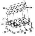
도 1A 및 1B는 일 예시에 따른 디바이스 내에 포함된 다층 전자기기 어셈블리의 개략화된 표현들이다. 도 1A는 디바이스의 주된 서브-어셈블리들의 분해 조립도이다. 서브어셈블리들은 다층 전자기기 어셈블리(multilayer electronics assembly; 10), 베이스 기판(base substrate; 20) 및 히트-싱크(heat-sink; 30)를 포함한다.1A and 1B are schematic representations of a multilayer electronics assembly included in a device according to one example. 1A is an exploded view of the main sub-assemblies of the device. Subassemblies include a multilayer electronics assembly (10), a base substrate (20) and a heat-sink (30).
이 예시에서, 베이스 기판(20)은 알루미늄 질화물(aluminum nitride; AlN) 직접 접합된 구리(direct bonded copper; DBC) 기판일 수 있고, 그것은 그것의 상면에 복수 개의 (예를 들어, 구리 트레이스 같은) 전도성 트레이스들(conductive traces 22), 그것의 상면에 접합된 복수 개의 (예를 들어, 전력 금속 산화물 반도체 전계 효과 트랜지스터들(power Metal Oxide Semiconductor Field Effect Transistors), MOSFETs 같은) 베어 다이(bare die; 24) 및 그것의 상면으로부터 연장하는 복수 개의 연결 포스트들(interconnecting posts; 26)을 포함한다.In this example, the
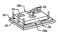
다층 전자기기 어셈블리(10)는 3차원으로 그 안에 내장된 별개의 전기 회로 부품들을 포함한다. 이하에서 보다 상세히 설명되는 것과 같이, 다층 전자기기 어셈블리(10)는 퓨전 접합 프로세스에 의해 형성되고 별개의 전기 회로 부품들은 퓨전 접합 전에 어셈블리의 내부 층들에 접합된다. 복수 개의 캐비티들(cavities; 14)은 기판(20)에 베어 다이(24)를 수용하기 위해 다층 전자기기 어셈블리(10)의 바닥면 상에 형성된다. 도 1B에 도시된 것과 같이, 다층 전자기기 어셈블리(10)는 또한 표면 장착 기술(surface mount technology)을 이용하여 부착된 더 높은 프로파일 부분들(higher profile parts)을 수용하기 위해 그것의 상면에 복수 개의 캐비티들(16)을 포함한다. 그러므로, 능동 부품들은 다층 전자기기 어셈블리(10)의 상측(10b)에, 또는 다층 전자기기 어셈블리(10)의 바닥 측(10a)에 부착될 수 있다.The
일 예시에서, 기판(20) 상의 베어 다이(24)는 나노실버 소결 기술(nanosilver sintering technique)로 다층 전자기기 어셈블리(10)에 부착된다. 예를 들어, 나노실버가 소결된 솔더 페이스트(nanosilver sintered solder paste)는 캐비티들(14) 내에 사용될 수 있다. 이 예시에서, 나노실버 소결은 나노실버 페이스트 내에 바인더(binder)를 베이크 아웃(bake out)하기 위해 대략 180℃로 램프되고(ramps) 그런 다음 나노실버 입자들을 소결하기 위해 10분 동안 대략 280℃로 온도를 증가시키는 온도 프로파일(temperature profile)로 획득된다. 결과적인 계면의(interfacial) "솔더(solder)" 조인트는 종래의 리드(lead) 또는 리드-프리(lead-free) 솔더보다 상당히 낮은 열 및 전기 저항, 반복된 열 사이클링으로 유도된 응력에 직면하여 개선된 무결성, 및 >900℃까지 '리플로우(reflow)'하지 않을 솔더 조인트를 구비한다. 후자의 특성은 전력 반도체 솔더 조인트들의 리플로우 없이 상측 부품들의 포스트-프로세스 솔더링 및 다층 전자기기 어셈블리(10)의 퓨전 접합 프로세스에 대한 노출을 잠재적으로 포함하는 포스트-프로세싱을 허용한다.In one example, the
전술된 것과 같이, 다층 전자기기 어셈블리(10)의 별개의 전기 회로 부품들은 퓨전 접합 전에 어셈블리의 내부 층들에 접합된다. 도 2는 퓨전 접합 전에 예시적인 다층 전자기기 어셈블리의 보다 상세한 측면도를 도시한다.As described above, the separate electrical circuit components of the
어셈블리의 바닥으로부터 시작해서, 제1 층(300)은 히트-싱크이다. 이 예시에서, 히트-싱크(300)는 다양한 열 인터페이스 옵션들(thermal interface options), 예를 들어 전도를 위한 장착 홀들(mounting holes; 310), 액체(미도시)를 위한 채널들, 또는 공기를 냉각시키기 위한 핀 핀(pin fin)/슬롯된 핀들(slotted fins)(미도시)을 지지하기 위해 주조될 수 있다(cast).Starting from the bottom of the assembly, the
제2 층은 이 예시에서 각각의 층에 구리로 도시된 베이스 층(base layer; 200)이다. 베이스 기판(20)과 같이, 베이스 층(200)은 알루미늄 질화물(AlN) 직접 접합된 구리(DBC) 기판으로 될 수 있다. 베이스 층(200)은 에폭시, 솔더(나노실버가 소결된 솔더, 또는 만약 히트-싱크가 퓨전 접합 프로세스 이후에 부착된다면, 표준 솔더(standard solder)), 또는, 만약 베이스 층(200)이 히트 싱크를 향하는 측 상에 구리로 클래드(clad)되지 않는다면, 퓨전 접합(전체 어셈블리를 위해 개별적으로 또는 단일의 작업 중 어느 하나)에 의해 히트-싱크(300)에 부착될 수 있다.The second layer is the
다층 전자기기 어셈블리(100)는 베이스 층(200)보다 위에 배치된다. 다층 전자기기 어셈블리(100)의 제1(가장 낮은) 층(110)은 반도체 다이들(510)의 상측 및 바닥 측들 사이에 스페이서(spacer) 및 연결 층(interconnect layer)으로 작용할 수 있다. 복수 개의 층들(120, 130, 140, 150, 160, 170, 및 180)은 제1 층(110)보다 위에 적층된다. 이 층들은 나노실버 소결 또는 전이 액상 접합(transient liquid phase bonding) 같은 디바이스 부착 기술에 의해 거기에 접합된 별개의 전자기기 부품들(520, 530, 및 560)을 포함할 수 있다. 별개의 전자기기 부품들(520)은 예를 들어 수동 별개의 레지스터, 캐패시터, 자기 디바이스 또는 능동 반도체 디바이스일 수 있다. 표면 장착 기술들은 상측에 추가적인 부품들(540 및 550)을 추가하기 위해 사용될 수 있다. 디바이스는 전력 연결부(power interconnect; 600)을 포함할 수 있고, 그것은 예를 들어 디바이스에 전력을 공급하기 위한 편평한 구리 리본 연결부(flat copper ribbon interconnect)일 수 있다.The
글래스 및 세라믹으로 채워진 폴리테트라플루오로에틸렌(PTFE) 같은 플루오로폴리머 복합체의 유전성(dielectric properties)은 고주파(radiofrequency) 적용에 적합한 전력 전자기기를 포함하는 다층 구조에 기여할 수 있다. 그러나, 전술된 것과 같이, 본 발명의 범위는 기판 물질로서 PTFE의 사용에 국한되지 않는다.Dielectric properties of fluoropolymer composites, such as glass and ceramic-filled polytetrafluoroethylene (PTFE), can contribute to a multi-layered structure comprising power electronics suitable for radiofrequency applications. However, as described above, the scope of the present invention is not limited to the use of PTFE as a substrate material.
이와 같이, 본 발명은 단지 퓨전 접합된 어셈블리들에 국한되지 않는다. 예를 들어, 또한 에폭시 유리섬유(epoxy fiberglass) 또는 폴리아미드를 사용하는 것과 같이 인쇄된 와이어 보드(printed wire board; PWB) 물질들로 마련된 층들을 활용하는 것에 의해 3차원으로 내장된 별개의 전기 회로 부품들을 구비하는 다층 모듈을 생성할 수 있다. 층들은 레진 매트릭스가 미리 주입된 강화 물질("프리프레그(prepreg)") 같은 제어된 접착제를 이용하여 조립될 수 있고, 나노실버 소결로 직접적으로 조립될 수 있고, 전이 액상 접합을 통해 직접적으로 조립될 수 있고, 또는 이러한 기술들의 조합을 이용하여 조립될 수 있다. 나노실버 소결 또는 전이 액상 접합으로 직접적인 조립을 하는 경우, 층들은 프로세싱(processing) 동안 아웃개싱(outgassing)을 허용하도록 충분한 양으로 이격될 수 있다. 만약 주위 노출이 염려된다면, 봉합재(encapsulant)가 층들 사이에 갭들을 밀폐하기 위해 사용될 수 있다.As such, the present invention is not limited to fusion bonded assemblies. Separate electrical circuits embedded in three dimensions by utilizing layers made of printed wire board (PWB) materials, such as, for example, also using epoxy fiberglass or polyamide. It is possible to create a multi-layer module having parts. The layers can be assembled using a controlled adhesive, such as a reinforcement material ("prepreg") pre-infused with a resin matrix, directly assembled by nanosilver sintering, and directly assembled through transitional liquid bonding. Can be, or can be assembled using a combination of these techniques. In the case of direct assembly with nanosilver sintering or transitional liquid phase bonding, the layers can be spaced in a sufficient amount to allow outgassing during processing. If ambient exposure is concerned, an encapsulant can be used to seal the gaps between the layers.
나노실버 소결 또는 전이 액상 접합은 개별적인 층에 디바이스들을 부착하고 그런 다음 하나의 층을 뒤이어 소결시켜 뒤이은 디바이스들을 부착하기 위해 요구되는 열에 의해 이미 부착된 디바이스들이 탈착되게 되는 것에 대한 우려 없앨 수 있다. 예를 들어, 디바이스들을 위한 접합 물질(나노실버 소결 또는 전이 액상 접합의 경우)은 디바이스들을 부착시키기 위한 프로세싱 다음에 상 전이를 겪게 되고 액체, 흐를 수 있는 또는 유연한 상태로 다시 변화하기 위해 상당히 더 높은 온도의 포스트-프로세싱을 요구한다. 이러한 포스트-프로세싱 상 전이 온도(post-processing state transition temperature)는 또한 초기에 디바이스들을 부착시키기 위해 요구되는 온도보다 실질적으로 더 높다. 결과적인 구조는 별개의 전기 회로 부품들을 포함하고 그것은 층들 내 캐비티들의 생성을 요구하지 않고 조립 후에 다층 모듈 내에 3차원으로 내장된다.Nanosilver sintering or transitional liquid phase bonding can eliminate the concern that devices already attached are desorbed by the heat required to attach the devices to individual layers and then sinter one layer to attach subsequent devices. For example, the bonding material for devices (in the case of nanosilver sintering or transition liquid phase bonding) undergoes a phase transition following processing to attach the devices and is significantly higher to change back to a liquid, flowable or flexible state. Post-processing of temperature is required. This post-processing state transition temperature is also substantially higher than the temperature required to initially attach the devices. The resulting structure includes discrete electrical circuit components, which do not require the creation of cavities in the layers and are embedded three-dimensionally in a multi-layer module after assembly.
Ⅲ. 제조 방법Ⅲ. Manufacturing method
다층 모듈 내에 3차원으로 별개의 전기 회로 부품들을 내장시키기 위한 몇몇의 작업들이 도 3A-3F, 4 및 5F를 참조하여 이하에서 설명된다.Several operations for embedding discrete electrical circuit components in three dimensions in a multi-layer module are described below with reference to FIGS. 3A-3F, 4 and 5F.
도 5의 제1 작업(800)에서, 다층 전자기기 어셈블리의 개별적인 층들이 제작된다. 예를 들어, 도 3A는 층들(110 및 200)을 도시한다. 층(110)은 글래스 및 세라믹이 채워진 (폴리테트라플루오로에틸렌(PTFE) 같은) 플루오로폴리머 복합체일 수 있다. 베이스 층(200)은 어느 한 측 상의 구리 같은, 반도체(410)를 포함한다. 전술된 것과 같이, 베이스 층(200)은 AIN 보드(board)로 형성된 직접 접합 구리 기판일 수 있다. 나노실버 소결이 디바이스 부착을 위해 사용되는 층들에서, 표면 최종 마감은 골드 또는 실버일 수 있다. 도 3A에 도시된 바와 같이, 개별적인 층들은, 층들 사이에 연결성을 고려하여 바이어스(vias; 420)를 포함할 수 있다.In the
도 5의 제2 작업(810)에서, 별개의 전기 회로 부품들은 개별적인 층들에 부착된다. 예를 들어, 도 3B는 별개의 전기 회로 부품들(520)을 도시하고, 이것은 개별적인 층(130)에 부착된, 레지스터들 및 캐패시터들 같은 수동 요소들(passive elements) 또는 작은 신호 능동 디바이스들(small signal active devices)일 수 있다. 별개의 전기 회로 부품들(520)은 나노실버 소결 도는 전이 액상 접합을 이용하여 층(130)에 접합될 수 있다. 전기 액상 접합의 예시는 Sang Won Yoon, Satoshi Yasuda, Michael D. Glover, Koji Shiozaki에 의한, "전기가 통하는 차량들의 고온 작동 전력 전자기기를 위한 고 신뢰성 니켈-주석 전이 액상 접합 기술(Highly Reliable Nickel-Tin Transient Liquid Phase Bonding Technology for High Temperature Operational Power Electronics in Electrified Vehicles)"에서 설명된다. 나노실버 소결의 예시는 국제공개 No. WO 2005/079353에서 설명된다.In the
본 예시에서, 별개의 전기 회로 부품들(520)은 도 4에 도시된 온도 프로파일을 이용하여, 나노실버 소결에 의해 개별적인 층(130)에 부착된다. 이 예시에서, 압력은 10 mm x 10 mm보다 작은 부품들의 다이 부착을 위해 사용되지 않는다.In this example, separate
도 5의 제3 작업(820)에서, 서브어셈블리는 접합을 위해 조립된다. 예를 들어, 도 3C는 베이스 층(200) 및 전력 반도체 다이(510)와 층들(110 및 120)의 조립을 도시한다. 연결 포스트들(430)은 층들의 정렬에 도움이 된다. 이 예시에서, 나노실버 솔더 페이스트는 각각의 층들(110, 120, 및 200) 상에 실크스크린된다(silkscreened). 예를 들어, 두께가 50㎛인 나노실버의 층이 실크스크린되고 공기가 건조되게 한다. 그런 다음, 10㎛인 나노실버의 층이 적용되고, 전력 반도체 다이(510)는 제 위치에 놓이고, 층들(200, 110 및 120)은 소결 프로세스를 위한 준비로 배치된다. 층(120)에는 전력 반도체 다이(510)의 주변부 주위 또는 위에 드릴된(drilled) 배출구들(vent holes; 122)이 도시된다. 이러한 배출구들(122)은 소결 프로세스 동안 나노실버 솔더 페이스트 내 용제들 및 바인더가 새어 나가게 한다.In the
이어서, 도 5의 830에서 도시된 것과 같이, 서브어셈블리의 요소들이 함께 접합된다. 예를 들어, 도 3D에 도시된 바와 같이, 압력이 플레이트들(710 및 720)에 작용된다. 플레이트(720)는 층(120)의 배출구들(122)과 정렬된 배출구들(722)을 포함한다. 압력은 용제들이 다이 아래로부터 베이크 아웃되고 배출구들(722)이 가스를 새어 나가게 하는 것을 담보하도록 작용된다. 이 예시에서, 대략 3-5 MPa은 10 mm x 10 mm보다 큰 다이가 사용될 때 나노실버 소결 프로세스를 위해 사용된다. 이 예시에서 프로파일은, 압력이 프로파일의 180℃, 10분 부분에 (및 180℃까지 램프(ramp) 동안 요구된다면/요구될 때) 적용되는 것을 제외하고, 필수적으로 도 4에 도시된 것과 동일하다. 그런 다음 압력은 275/300℃까지 차지하기 전에 제거될 수 있다.Subsequently, the elements of the subassembly are joined together, as shown at 830 of FIG. 5. For example, as shown in FIG. 3D, pressure is applied to the
이어서, 도 5의 840에서 도시된 것과 같이, 층들이 퓨전 접합을 위해 조립된다. 예를 들어, 도 3E에 도시된 바와 같이, 남아 있는 층들(130, 140, 150, 160, 170, 및 180)은 함께 소결되지 않는 층들(110, 120, 및 200)의 서브-어셈블리와 함께 적층된다. 이러한 층들은 그런 다음 퓨전 접합된다(850, 도 5). 퓨전 접합은 일반적으로 오토클래이브(autoclave) 또는 유압 프레스 내에서 PTFE 복합체 용융점을 지나 기판 층들을 가열하면서 동시적으로, 미리 정해진 양의 압력을 적용하는 것에 의해, 바람직하게 기계적으로, 등압으로(isostatically), 또는 양쪽의 조합으로 성취된다. 층들의 정렬은 PTFE 레진이 점성 액체로 상태를 변화시키고 인접한 층들이 압력하에서 퓨즈(fuse)함에 따라 흐름을 안정화시키기 위해, 바람직하게 3개 내지 8개 그러나 그 이상으로, (본 예시에서 연결 포스트들(430) 같은) 복수 개의 핀들을 구비하는 정밀 고정물(precision fixture)에 의해 일반적으로 고정된다. 접합되는 적층의 크기에 따라, 적층의 정렬에 대한 핀 배치는 바람직하게 삼각형 또는 사각형이다. 핀들 그 자체는 바람직하게 원형, 정사각형, 직사각형, 타원형 또는 다이아몬드 형상이나, 다른 형상들을 구비할 수 있다.The layers are then assembled for fusion bonding, as shown at 840 in FIG. 5. For example, as shown in FIG. 3E, the remaining
별개의 전기 회로 부품들(510, 520, 및 560)이 나노실버 소결 또는 전이 액상 접합에 의해 개별적인 층들에 부착되었으므로, 별개의 전기 회로 부품들(510, 520, 및 560)은 퓨전 접합 프로세스 동안 모듈 내 전도성 경로들에 접합된 채로 있을 수 있다. 예를 들어, 전이 액상 접합에 의해 형성된 합금의 용융 온도 및 나노실버 소결로 형성된 접합의 용융점은 퓨전 접합을 위한 PTFE 복합체 용융점을 획득하기 위해 필요한 온도를 훨씬 초과한다. 결과적인 3차원, 단일, 다층 전자기기 모듈(1000)이 도 3F에 도시된다. 다층 전자기기 모듈(1000)은 퓨전 접합된 블록 내에 3차원으로 내장된 복수 개의 별개의 전기 회로 부품들(510, 520, 및 560)을 포함한다. 종래의 다층, 퓨전 접합된 모듈들과 달리, 도 3F의 모듈(1000)은 층들 내에 적층된 별개의 전기 회로 부품들을 포함하여 별개의 전기 회로 부품들이 수직 차원(vertical dimension)으로 겹친다. 게다가, 별개의 전기 회로 부품들은 추가적인 포스트-퓨전 드릴링(post-fusion drilling) 및 플레이팅(plating)에 대한 요구 없이 둘러싸는 층들에 전기적으로 연결된다. 더 나아가, 습기 유입에 대한 내성은 퓨전 접합을 통해 형성된 단일 구조의 무결정에 의해 지원된다.Since the separate
퓨전 접합이 수행된 후에, 히트-싱크 및 상측 표면 장착 부품들이 부착된다(860, 도 5). 예를 들어, 도 3F에 도시된 바와 같이, 히트-싱크(300)는 다층 전자기기 모듈(1000) 아래에 부착되고, 상측 표면 장착 기술 부분들(top-side surface mount technology parts; 540 및 550)은 다층 전자기기 모듈(1000)의 상면에 부착된다. 만약 베이스 층(200)이 히트 싱크를 향하는 측 상에 구리로 클래드되지 않는다면, 베이스 층(200)에 대한 히트-싱크(300)를 퓨전 접합하는 것에 의해 낮은 열 저항이 얻어질 수 있다. 일 예시에서, 이것은 도 3E를 참조하여 기술된 퓨전 접합 작업의 일부로서 성취될 수 있다. 이 경우에, 히트-싱크(300)는 모듈들을 멀리 절단하는 것을 수월하게 하기 위해 모듈들 사이에 '웹(web)' 매트릭스로 설계될 수 있다. 이러한 절단은 워터 제트 절단(water jet cutting)에 의해 달성될 수 있다. 다른 예시에서, 히트-싱크(300)는 Al 스킨(skin)에 의해 함께 유지되는 단면(sectional) 모듈들 내 AlSiC 주조일 수 있어 오직 Al 스킨만이 절단될 필요가 있다. 다른 예시에서, 히트-싱크(300)는 도 3E에 도시된 어셈블리에 솔더될 수 있거나, 거기에 접합될 수 있다.After fusion bonding is performed, heat-sink and top surface mounting components are attached (860, FIG. 5). For example, as shown in FIG. 3F, the heat-
전술된 다양한 실시예들은 추가적인 실시예들을 제공하기 위해 결합될 수 있다. 이 명세서에서 언급된 모든 미국 특허들, 미국 특허 출원 공개들, 미국 특허 출원들, 외국 특허 출원들 및 비-특허 공개들은 그 전체로, 참조로 여기에 포함된다. 실시예들의 측면들은, 추가적인 실시예들을 제공하기 위해 다양한 특허들, 출원들 및 공개들의 개념들을 활용할 필요가 있다면, 변경될 수 있다.The various embodiments described above can be combined to provide additional embodiments. All U.S. patents, U.S. patent application publications, U.S. patent applications, foreign patent applications, and non-patent publications mentioned in this specification are incorporated herein by reference in their entirety. Aspects of the embodiments can be modified if necessary to utilize the concepts of various patents, applications and publications to provide additional embodiments.
이것 및 다른 변화들이 전술된 설명의 측면에서 실시예들에 대해 이루어질 수 있다. 일반적으로, 다음의 청구항들에서, 사용되는 용어들은 명세서 및 청구항들에 개시된 구체적인 실시예들에 대해 청구항들을 제한하도록 해석되지 않으며, 그러한 청구항들이 붙여지는 균등물의 전체 범위와 같이 모든 가능한 실시예들을 포함하는 것으로 해석되어야 한다. 따라서, 청구항들은 본 발명에 의해 제한되지 않는다.This and other changes can be made to the embodiments in terms of the foregoing description. In general, in the following claims, the terms used are not to be construed to limit the claims to the specific embodiments disclosed in the specification and claims, and include all possible embodiments, such as the full scope of equivalents to which such claims are attached. It should be interpreted as. Accordingly, the claims are not limited by the present invention.
10: 다층 전자기기 어셈블리
120, 130, 140, 150, 160, 170, 180: 층
10a: 상측
10b: 바닥 측
14, 16: 캐비티
20, 200: 베이스 기판
22: 전도성 트레이스
24: 베어 다이
26: 연결 포스트
30, 300: 히트-싱크
310: 장착 홀
410: 반도체
420: 바이어스
510: 전력 반도체 다이
520, 530, 560: 별개의 전자기기 부품
600: 전력 연결부10: multilayer electronics assembly
120, 130, 140, 150, 160, 170, 180: floor
10a: upper side
10b: bottom side
14, 16: cavity
20, 200: base substrate
22: conductive trace
24: bare die
26: Connection post
30, 300: Heat-sink
310: mounting hole
410: semiconductor
420: bias
510: power semiconductor die
520, 530, 560: separate electronics components
600: power connection
Claims (53)
Translated fromKorean상기 다층 전자기기 어셈블리는,
제1 방향으로 적층된 복수 개의 기판 층들 - 상기 복수 개의 기판 층들은 각각 퓨전 접합 공정에 의해서 복수 개의 기판 층들 중 적어도 하나의 인접한 기판 층에 접합됨 -;
접합 물질 - 상기 접합 물질은 상기 접합 물질이 흐를 수 있게 되는 초기 전이 온도, 및 상기 접합 물질이 초기에 흐르게 된 다음에 경화된 후에 뒤이어서 흐를 수 있게 되는 뒤이은 전이 온도를 구비하고, 상기 초기 전이 온도는 상기 뒤이은 전이 온도보다 낮고, 퓨전 접합 공정 시에 상기 복수 개의 기판 층들의 용융점은 상기 뒤이은 전이 온도보다 낮음 -;
상기 접합 물질에 의해 상기 복수 개의 기판 층들 중 제1 기판 층에 접합되는 제1 별개의 전기 회로 부품; 및
상기 접합 물질에 의해 상기 복수 개의 기판 층들 중 제2 기판 층에 접합되는 제2 별개의 전기 회로 부품 - 상기 제2 별개의 전기 회로 부품은 제1 방향으로 상기 제1 별개의 전기 회로 부품에 겹쳐짐 -;
을 포함하는, 다층 전자기기 어셈블리.
In the multilayer electronics assembly,
The multilayer electronic device assembly,
A plurality of substrate layers stacked in a first direction, each of the plurality of substrate layers being bonded to at least one adjacent substrate layer of the plurality of substrate layers by a fusion bonding process;
Bonding material-the bonding material has an initial transition temperature at which the bonding material can flow, and a subsequent transition temperature at which the bonding material is initially flowed and then cured and then allowed to flow, and the initial transition temperature. Is lower than the subsequent transition temperature, and the melting point of the plurality of substrate layers during the fusion bonding process is lower than the subsequent transition temperature-;
A first separate electrical circuit component bonded to the first substrate layer of the plurality of substrate layers by the bonding material; And
A second separate electrical circuit component bonded to a second one of the plurality of substrate layers by the bonding material, the second separate electrical circuit component overlapping the first distinct electrical circuit component in a first direction -;
Multilayer electronic device assembly comprising a.
상기 접합 물질은 상기 뒤이은 전이 온도에 도달되기 직전에 고체인, 다층 전자기기 어셈블리.
According to claim 1,
Wherein the bonding material is solid just before reaching the subsequent transition temperature.
상기 접합 물질은 나노실버 소결된 솔더인, 다층 전자기기 어셈블리.
The method according to claim 1 or 2,
The bonding material is a nano-silver sintered solder, multi-layer electronics assembly.
상기 접합 물질은 전이 액상 합금인, 다층 전자기기 어셈블리.
The method according to claim 1 or 2,
The bonding material is a transition liquid alloy, multilayer electronics assembly.
상기 제1 별개의 전기 회로 부품은 수동 별개의 레지스터, 캐패시터, 자기 디바이스 및 능동 반도체 디바이스 중 하나인, 다층 전자기기 어셈블리.
The method according to claim 1 or 2,
The first discrete electrical circuit component is one of passive discrete resistors, capacitors, magnetic devices and active semiconductor devices, a multilayer electronics assembly.
상기 다층 전자기기 어셈블리는,
복수 개의 적층된 기판 층들 - 상기 복수 개의 적층된 기판 층들은 각각 퓨전 접합 공정에 의해서 복수 개의 기판 층들 중 적어도 하나의 인접한 기판 층에 접합됨 -;
상기 복수 개의 기판 층들 중 제1 층에 접합되는 제1 별개의 전기 회로 부품 - 900℃보다 높은 리플로우 온도를 갖는 계면의솔더 조인트를 형성하고 제1 층 및 제1 별개의 전기 회로 부품 사이에 개재된 접합 물질을 사용하고, 상기 접합 물질이 흐를 수 있게 되는 상기 리플로우 온도는 상기 기판 층의 퓨전 접합 온도 및 상기 접합 물질의 초기 플로우 온도보다 높고, 상기 접합 물질의 초기 플로우 온도는 상기 기판 층의 퓨전 접합 전에 상기 제1 층 및 상기 제1 별개의 전기 회로 부품을 접합시키기 위해서 상기 접합 물질이 흐를 수 있게 되는 온도임 -;
상기 제1 층 및 상기 제1 별개의 전기 회로 부품의 접합 동안 가스가 새어 나가게 하도록 작동 가능하게 구성되는 복수 개의 배출구;
를 포함하는, 다층 전자기기 어셈블리.
In the multilayer electronics assembly,
The multilayer electronic device assembly,
A plurality of stacked substrate layers, each of the plurality of stacked substrate layers being bonded to at least one adjacent substrate layer of the plurality of substrate layers by a fusion bonding process;
A first separate electrical circuit component bonded to a first one of the plurality of substrate layers-at an interface having a reflow temperature higher than 900 ° C The reflow temperature that forms a solder joint and uses a bonding material interposed between the first layer and the first discrete electrical circuit component, and the reflow temperature at which the bonding material can flow is determined by the fusion bonding temperature of the substrate layer and the bonding material. Higher than the initial flow temperature of, and the initial flow temperature of the bonding material is a temperature at which the bonding material can flow to bond the first layer and the first separate electrical circuit component before fusion bonding of the substrate layer − ;
A plurality of outlets operatively configured to cause gas to escape during bonding of the first layer and the first distinct electrical circuit component;
Multilayer electronic device assembly comprising a.
상기 복수 개의 기판 층들 중 제2 층에 접합되는 제2 별개의 전기 회로 부품;
을 더 포함하는, 다층 전자기기 어셈블리.
The method of claim 7,
A second separate electrical circuit component bonded to a second layer of the plurality of substrate layers;
Multi-layer electronic device assembly further comprising.
상기 복수 개의 기판 층들은 제1 방향으로 적층되고, 상기 제1 별개의 전기 회로 부품은 제1 방향으로 상기 제2 별개의 전기 회로 부품에 겹쳐지는, 다층 전자기기 어셈블리.
The method of claim 8,
Wherein the plurality of substrate layers are stacked in a first direction, and the first distinct electrical circuit component overlaps the second distinct electrical circuit component in a first direction.
상기 복수 개의 기판 층들은 제1 방향으로 적층되고, 상기 제1 별개의 전기 회로 부품은 복수 개의 적층된 기판 층들 중 인접한 층들 사이에 위치되는, 다층 전자기기 어셈블리.
The method of claim 7,
Wherein the plurality of substrate layers are stacked in a first direction, and the first separate electrical circuit component is located between adjacent layers of the plurality of stacked substrate layers.
상기 기판 층들은 플루오로폴리머 복합체를 포함하는, 다층 전자기기 어셈블리.
The method of claim 7,
Wherein the substrate layers comprise a fluoropolymer composite.
상기 접합 물질은 상기 리플로우 온도에 도달되기 직전에 고체인, 다층 전자기기 어셈블리.
The method of claim 7,
The bonding material is solid, just before reaching the reflow temperature, a multilayer electronics assembly.
상기 접합 물질은 나노실버 소결된 솔더인, 다층 전자기기 어셈블리.
The method of claim 7,
The bonding material is a nano-silver sintered solder, multi-layer electronics assembly.
상기 접합 물질은 전이 액상 접합 함금인, 다층 전자기기 어셈블리.
The method of claim 7,
The bonding material is a transitional liquid bonding alloy, multilayer electronics assembly.
상기 제1 별개의 전기 회로 부품은 수동 별개의 레지스터, 캐패시터, 자기 디바이스 및 능동 반도체 디바이스 중 하나인, 다층 전자기기 어셈블리.
The method of claim 7,
The first discrete electrical circuit component is one of passive discrete resistors, capacitors, magnetic devices and active semiconductor devices, a multilayer electronics assembly.
상기 복수 개의 적층된 기판 층들 중 하나는 일차 기판이고, 상기 일차 기판에 전력 반도체가 다이 접합되고, 상기 일차 기판 상에 다른 기판 층들이 적층되고, 상기 일차 기판으로부터 가장 멀리 위치된 상기 복수 개의 기판 층들 중 하나의 외부 표면에 능동 전자기기 부품이 부착되는, 다층 전자기기 어셈블리.
The method of claim 7,
One of the plurality of stacked substrate layers is a primary substrate, a power semiconductor is die bonded to the primary substrate, other substrate layers are stacked on the primary substrate, and the plurality of substrate layers positioned farthest from the primary substrate A multilayer electronics assembly, wherein an active electronics component is attached to one of the outer surfaces.
상기 제1 별개의 전기 회로 부품 및 상기 제1 층 사이에 개재된 접합 물질은 상기 기판 층들의 퓨전 접합 온도보다 높은 제1 용융점을 갖는 제1 물질이고, 상기 다층 전자기기 어셈블리는 상기 기판 층들의 퓨전 접합 온도보다 높은 제2 용융점을 갖는 제2 물질에 의해서 상기 복수 개의 기판 층들 중 제2 층에 접합되는 제2 별개의 전기 회로 부품을 더 포함하는, 다층 전자기기 어셈블리.
The method of claim 16,
The bonding material interposed between the first discrete electrical circuit component and the first layer is a first material having a first melting point higher than the fusion bonding temperature of the substrate layers, and the multilayer electronics assembly is a fusion of the substrate layers. And a second separate electrical circuit component bonded to a second one of the plurality of substrate layers by a second material having a second melting point higher than a junction temperature.
복수 개의 적층된 기판 층들 - 상기 복수 개의 기판 층들은 각각 상기 복수 개의 기판 층들 적어도 하나의 인접한 기판 층에 퓨전 접합되어 단일 블록을 형성함 -;
상기 복수 개의 기판 층들 중 제1 층에 접합되는 제1 별개의 전기 회로 부품;
상기 제1 층 및 상기 제1 별개의 전기 회로 부품 사이에 접합을 제공하는, 상기 제1 층 및 상기 제1 별개의 전기 회로 부품 사이에 개재된 접합 물질 - 상기 접합 물질은 상기 기판 층들의 퓨전 접합 온도보다 높은 상기 접합 물질이 흐를 수 있게 되는 리플로우 온도를 가져서, 상기 접합 물질이 상기 퓨전 접합 온도에 노출되는 경우에도 상기 제1 층에 접합된 상기 제1 별개의 전기 회로 부품이 견고하게(solidly) 유지됨; 및
상기 복수 개의 기판 층들 중 제2 층에 제공된 복수 개의 배출구 - 상기 복수 개의 배출구는 상기 제1 층에 대한 상기 제1 별개의 전기 회로 부품의 접합 동안 가스가 새어 나가게 하도록 작동 가능하게 구성되고, 상기 복수 개의 배출구는 함께 퓨전 접합된 복수 개의 기판 층들에 의해서 형성된 단일 블록의 내부에 밀폐됨 -;
를 포함하는, 다층 전자기기 어셈블리.
In the multilayer electronics assembly,
A plurality of stacked substrate layers, each of the plurality of substrate layers being fusion bonded to at least one adjacent substrate layer of the plurality of substrate layers to form a single block;
A first separate electrical circuit component bonded to a first one of the plurality of substrate layers;
A bonding material interposed between the first layer and the first discrete electrical circuit component, providing a bonding between the first layer and the first discrete electrical circuit component, wherein the bonding material is a fusion bonding of the substrate layers The first distinct electrical circuit component bonded to the first layer is solidly solid even when the bonding material is exposed to the fusion bonding temperature by having a reflow temperature at which the bonding material above the temperature can flow. ) Maintained; And
A plurality of outlets provided in a second layer of the plurality of substrate layers, the plurality of outlets being operatively configured to allow gas to escape during bonding of the first separate electrical circuit component to the first layer, the plurality of outlets The two outlets are sealed inside a single block formed by a plurality of substrate layers fusion bonded together;
Multilayer electronic device assembly comprising a.
상기 복수 개의 기판 층들 중 제2 층에 접합되는 제2 별개의 전기 회로 부품;
을 더 포함하는, 다층 전자기기 어셈블리.
The method of claim 18,
A second separate electrical circuit component bonded to a second layer of the plurality of substrate layers;
Multi-layer electronic device assembly further comprising.
상기 복수 개의 기판 층들은 제1 방향으로 적층되고, 상기 제1 별개의 전기 회로 부품은 상기 복수 개의 기판 층들 중 상기 제1 층에 대한 상기 제1 별개의 전기 회로 부품의 하부 부착 면에 접합되고, 상기 제2 별개의 전기 회로 부품은 상기 복수 개의 기판 층들 중 상기 제2 층에 상기 제2 별개의 전기 회로 부품의 하부 부착 면에 접합되며, 상기 제1 별개의 전기 회로 부품은 제1 방향으로 상기 제2 별개의 전기 회로 부품에 겹쳐지며, 상기 제1 및 제2 별개의 전기 회로 부품의 하부 부착 면은 상기 복수 개의 기판 층들이 적층되는 제1 방향에 맞춰서 동일한 방향을 향하는, 다층 전자기기 어셈블리.
The method of claim 19,
The plurality of substrate layers are stacked in a first direction, and the first distinct electrical circuit component is bonded to a lower attachment surface of the first distinct electrical circuit component to the first layer of the plurality of substrate layers, The second discrete electrical circuit component is bonded to the second attachment layer of the second distinct electrical circuit component to the second layer of the plurality of substrate layers, and the first distinct electrical circuit component is disposed in the first direction. A multilayer electronics assembly, overlaid on a second distinct electrical circuit component, wherein the lower attachment surfaces of the first and second distinct electrical circuit components face the same direction in alignment with the first direction in which the plurality of substrate layers are stacked.
상기 복수 개의 기판 층들은 제1 방향으로 적층되고, 상기 제1 별개의 전기 회로 부품은 복수 개의 적층된 기판 층들 중 인접한 층들 사이에 위치되는, 다층 전자기기 어셈블리.
The method of claim 18,
Wherein the plurality of substrate layers are stacked in a first direction, and the first separate electrical circuit component is located between adjacent layers of the plurality of stacked substrate layers.
상기 기판 층들은 플루오로폴리머 복합체를 포함하는, 다층 전자기기 어셈블리.
The method of claim 18,
Wherein the substrate layers comprise a fluoropolymer composite.
상기 접합 물질은 상기 제1 층 및 상기 제1 별개의 전기 회로 부품을 접합시키기 위해서 상기 접합 물질이 흐를 수 있게 되는 초기 플로우 온도를 갖는 적어도 하나의 물질로 형성되고, 상기 초기 플로우 온도는 상기 리플로우 온도보다 낮은, 다층 전자기기 어셈블리.
The method of claim 18,
The bonding material is formed of at least one material having an initial flow temperature through which the bonding material can flow to bond the first layer and the first distinct electrical circuit component, and the initial flow temperature is the reflow. Multi-level electronics assembly, below temperature.
상기 접합 물질은 상기 리플로우 온도에 도달되기 직전에 고체인, 다층 전자기기 어셈블리.
The method of claim 18,
The bonding material is solid, just before reaching the reflow temperature, a multilayer electronics assembly.
상기 접합 물질은 나노실버 소결된 솔더인, 다층 전자기기 어셈블리.
The method of claim 18,
The bonding material is a nano-silver sintered solder, multi-layer electronics assembly.
상기 접합 물질은 전이 액상 접합 함금인, 다층 전자기기 어셈블리.
The method of claim 18,
The bonding material is a transitional liquid bonding alloy, multilayer electronics assembly.
상기 제1 별개의 전기 회로 부품은 수동 별개의 레지스터, 캐패시터, 자기 디바이스 및 능동 반도체 디바이스 중 하나인, 다층 전자기기 어셈블리.
The method of claim 18,
The first discrete electrical circuit component is one of passive discrete resistors, capacitors, magnetic devices and active semiconductor devices, a multilayer electronics assembly.
상기 단일 블록 내에 내장된 복수 개의 별개의 전기 회로 부품들 - 상기 복수 개의 별개의 전기 회로 부품들은 각각 접합 물질에 의해서 상기 블록에 접합되고, 상기 접합 물질은 상기 제1 온도보다 높은 제2 온도에서, 상기 접합 물질이 흐를 수 있게 되는 리플로우 온도를 가져서, 상기 접합 물질이 상기 제1 온도에 노출되는 경우에도 상기 블록에 접합된 상기 복수 개의 별개의 전기 회로 부품들이 견고하게 유지됨 -;
을 포함하고,
복수 개의 배출구가 상기 단일 블록의 내부에 제공 및 밀폐되고, 상기 복수 개의 배출구는 상기 접합 물질에 의해서 상기 블록에 대한 상기 복수 개의 별개의 전기 회로 부품들의 접합 동안 가스가 세어 나가게 하도록 작동 가능하게 구성되는, 다층 전자기기 모듈.
A three-dimensional, single block of first material having a melting point at a first temperature; And
A plurality of separate electrical circuit components embedded in the single block-the plurality of separate electrical circuit components are each joined to the block by a bonding material, the bonding material at a second temperature higher than the first temperature, Having a reflow temperature through which the bonding material can flow, so that the plurality of separate electrical circuit components bonded to the block are held firmly even when the bonding material is exposed to the first temperature;
Including,
A plurality of outlets are provided and sealed inside the single block, the plurality of outlets being operatively configured to cause gas to leak out during bonding of the plurality of separate electrical circuit components to the block by the bonding material. , Multilayer electronics module.
상기 단일 블록은 상면, 바닥면, 및 복수 개의 측면들에 의해서 정의된 외부 표면을 포함하고, 상기 제1 물질은 상기 복수 개의 별개의 전기 회로 부품들 중 적어도 하나의 제1 전기 회로 부품을 완전히 둘러싸서, 상기 제1 물질이 상기 단일 블록의 외부 표면 상의 임의의 지점 및 상기 복수 개의 별개의 전기 회로 부품들 중 제1 전기 회로 부품의 모든 측면들 사이에 위치되는, 다층 전자기기 모듈.
The method of claim 28,
The single block includes an outer surface defined by a top surface, a bottom surface, and a plurality of side surfaces, and the first material completely surrounds a first electrical circuit component of at least one of the plurality of discrete electrical circuit components. Inexpensively, the multi-layer electronics module, wherein the first material is located between any side of the outer surface of the single block and all sides of the first one of the plurality of separate electrical circuit components.
상기 제1 물질은 상기 복수 개의 별개의 전기 회로 부품들 중 제1 전기 회로 부품에 직접적으로 접촉하지 않는, 다층 전자기기 모듈.
The method of claim 29,
The first material does not directly contact the first electrical circuit component of the plurality of separate electrical circuit components, multilayer electronics module.
상기 복수 개의 별개의 전기 회로 부품들은 상기 블록에 대한 제1 별개의 전기 회로 부품의 하부 부착 면에 접합되는 제1 별개의 전기 회로 부품, 상기 블록에 대한 제2 별개의 전기 회로 부품의 하부 부착 면에 접합되는 제2 별개의 전기 회로 부품, 및 상기 블록에 대한 제3 별개의 전기 회로 부품의 하부 부착면에 접합되는 제3 별개의 전기 회로 부품을 포함하고, 상기 제1 별개의 전기 회로 부품은 제1 방향으로 제2 별개의 전기 회로 부품에 겹쳐지고, 상기 제1 및 제2 별개의 전기 회로 부품의 하부 부착 면은 상기 제1 방향과 맞춰서 동일한 방향을 향하고, 상기 제1 별개의 전기 회로 부품은 상기 제1 방향과 수직하는 제2 방향으로 상기 제3 별개의 전기 회로 부품에 겹쳐지고, 상기 제1 방향은 상기 다층 전자기기 모듈의 두께 방향으로 되는, 다층 전자기기 모듈.
The method of claim 28,
The plurality of separate electrical circuit components are first separate electrical circuit components that are joined to the bottom attachment surface of the first separate electrical circuit component to the block, and the bottom attachment surface of the second separate electrical circuit components to the block. And a second separate electrical circuit component bonded to a lower attachment surface of a third distinct electrical circuit component to the block, wherein the first distinct electrical circuit component is Superimposed on a second distinct electrical circuit component in a first direction, the lower attachment surfaces of the first and second distinct electrical circuit components facing the same direction in alignment with the first direction, and the first distinct electrical circuit component Is superimposed on the third separate electrical circuit component in a second direction perpendicular to the first direction, the first direction being in the thickness direction of the multilayer electronic device module, the multilayer electronic device module.
상기 제1 물질은 플루오로폴리머 복합체인, 다층 전자기기 모듈.
The method of claim 28,
The first material is a fluoropolymer composite, multilayer electronics module.
상기 접합 물질은 초기 플로우 온도를 갖는 적어도 하나의 물질로 형성되고, 상기 초기 플로우 온도에서 상기 접합 물질은 제1 층 및 상기 별개의 전기 회로 부품을 접합시키도록 흐를 수 있게 되며, 상기 초기 플로우 온도는 상기 제2 온도보다 낮은, 다층 전자기기 모듈.
The method of claim 28,
The bonding material is formed of at least one material having an initial flow temperature, and at the initial flow temperature, the bonding material is allowed to flow to bond the first layer and the separate electrical circuit component, wherein the initial flow temperature is A multilayer electronic device module, which is lower than the second temperature.
상기 접합 물질은 상기 제2 온도에 도달되기 직전에 고체인, 다층 전자기기 모듈.
The method of claim 28,
The bonding material is solid just before reaching the second temperature, the multilayer electronics module.
상기 접합 물질은 나노실버 소결된 솔더인, 다층 전자기기 모듈.
The method of claim 28,
The bonding material is a nano-silver sintered solder, multilayer electronics module.
상기 접합 물질은 전이 액상 접합 함금인, 다층 전자기기 모듈.
The method of claim 28,
The bonding material is a transition liquid bonding alloy, a multilayer electronic device module.
상기 복수 개의 별개의 전기 회로 부품들은 수동 별개의 레지스터, 캐패시터, 자기 디바이스 및 능동 반도체 디바이스 중 하나인, 다층 전자기기 모듈.
The method of claim 28,
The plurality of discrete electrical circuit components are one of passive discrete resistors, capacitors, magnetic devices and active semiconductor devices, multilayer electronics modules.
제1 방향으로 적층된 복수 개의 기판 층들 - 상기 복수 개의 기판 층들은 각각 상기 복수 개의 기판 층들 중 적어도 하나의 인접한 기판 층에 접합되어 단일 블록을 형성함 -;
접합 물질 - 상기 접합 물질은 상기 접합 물질이 초기에 흐를 수 있게 되는 초기 전이 온도 및 상기 접합 물질이 초기에 흐르게 된 다음에 경화된 후에 뒤이어서 흐를 수 있게 되는 뒤이은 전이 온도를 갖고, 상기 초기 전이 온도는 상기 뒤이은 전이 온도보다 낮음 -;
상기 접합 물질에 의해서 상기 복수 개의 기판 층들 중 제1 층에 접합되는 제1 별개의 전기 회로 부품;
상기 접합 물질에 의해서 상기 복수 개의 기판 층들 중 제2 층에 접합되는 제2 별개의 전기 회로 부품 - 상기 제2 별개의 회로 부품은 제1 방향으로 상기 제1 별개의 전기 회로 부품에 겹쳐짐 -;
상기 복수 개의 기판 층들 중 적어도 하나에 제공된 복수 개의 배출구 - 상기 복수 개의 배출구는 상기 접합 물질에 의해서 상기 제1 층에 대한 상기 제1 별개의 전기 회로 부품의 접합 동안 가스가 새어 나가게 하도록 작동 가능하게 구성되고, 상기 복수 개의 배출구는 상기 단일 블록의 내부에 밀폐됨 -;
를 포함하는, 다층 전자기기 어셈블리.
In the multilayer electronics assembly,
A plurality of substrate layers stacked in a first direction, each of the plurality of substrate layers being bonded to at least one adjacent substrate layer of the plurality of substrate layers to form a single block;
Bonding material-the bonding material has an initial transition temperature at which the bonding material can initially flow, and a subsequent transition temperature at which the bonding material is initially flowed and then cured and then allowed to flow. Is lower than the subsequent transition temperature-;
A first separate electrical circuit component bonded to the first of the plurality of substrate layers by the bonding material;
A second separate electrical circuit component bonded to the second layer of the plurality of substrate layers by the bonding material, the second distinct circuit component overlapping the first distinct electrical circuit component in a first direction;
A plurality of outlets provided in at least one of the plurality of substrate layers, the plurality of outlets being operatively configured to cause gas to escape during bonding of the first separate electrical circuit component to the first layer by the bonding material And the plurality of outlets are sealed inside the single block-;
Multilayer electronic device assembly comprising a.
상기 접합 물질은 상기 뒤이은 전이 온도에 도달되기 직전에 고체인, 다층 전자기기 어셈블리.
The method of claim 38,
Wherein the bonding material is solid just before reaching the subsequent transition temperature.
상기 접합 물질은 나노실버 소결된 솔더인, 다층 전자기기 어셈블리.
The method of claim 38,
The bonding material is a nano-silver sintered solder, multi-layer electronics assembly.
상기 접합 물질은 전이 액상 접합 함금인, 다층 전자기기 어셈블리.
The method of claim 38,
The bonding material is a transitional liquid bonding alloy, multilayer electronics assembly.
상기 제1 별개의 전기 회로 부품은 수동 별개의 레지스터, 캐패시터, 자기 디바이스 및 능동 반도체 디바이스 중 하나인, 다층 전자기기 어셈블리.
The method of claim 38,
The first discrete electrical circuit component is one of passive discrete resistors, capacitors, magnetic devices and active semiconductor devices, a multilayer electronics assembly.
상기 제1 별개의 전기 회로 부품은 상기 제1 층에 대한 상기 제1 별개의 전기 회로 부품의 하부 부착 면에 접합되고, 상기 제2 별개의 전기 회로 부품은 상기 복수 개의 기판 층들 중 상기 제2 층에 상기 제2 별개의 전기 회로 부품의 하부 부착 면에 접합되며, 상기 제2 별개의 전기 회로 부품은 제1 방향으로 상기 제1 별개의 전기 회로 부품에 겹쳐지며, 상기 제1 및 제2 별개의 전기 회로 부품의 하부 부착 면은 상기 제1 방향과 맞춰서 동일한 방향을 향하는, 다층 전자기기 어셈블리.
The method of claim 38,
The first discrete electrical circuit component is bonded to a bottom attachment surface of the first distinct electrical circuit component to the first layer, and the second distinct electrical circuit component is the second layer of the plurality of substrate layers. To the lower attachment surface of the second distinct electrical circuit component, the second distinct electrical circuit component overlaps the first distinct electrical circuit component in a first direction, and the first and second distinct A multilayer electronics assembly, wherein the lower attachment surface of the electrical circuit component faces the same direction in alignment with the first direction.
일차 기판 - 전력 반도체 다이가 상기 일차 기판에 접합됨 -;
상기 일차 기판 상에 적층되고 서로 퓨전 접합되어 단일 블록을 형성하는 복수 개의 이차 기판들 - 제1 별개의 전기 회로 부품은 기판 층들의 퓨전 접합 온도보다 높은 제1 용융점을 갖는 제1 물질에 의해서 상기 복수 개의 이차 기판들 중 제1 기판에 접합되어, 퓨전 접합 온도에 상기 제1 물질이 노출되는 경우에도 상기 제1 기판에 접합된 상기 제1 별개의 전기 회로 부품이 견고하게 유지되고, 제2 별개의 전기 회로 부품은 기판 층들의 퓨전 접합 온도보다 높은 제2 용융점을 갖는 제2 물질에 의해서 상기 복수 개의 이차 기판들 중 제2 기판에 접합되어, 퓨전 접합 온도에 상기 제2 물질이 노출되는 경우에도 상기 제2 기판에 접합된 상기 제2 별개의 전기 회로 부품이 견고하게 유지되며, 상기 복수 개의 이차 기판들 중 적어도 하나에 복수 개의 배출구가 제공되고, 상기 복수 개의 배출구는 상기 일차 기판에 상기 전력 반도체 다이의 접합 동안 가스가 새어 나가게 하도록 작동 가능하게 구성되고, 상기 복수 개의 배출구는 상기 단일 블록의 내부에 밀폐됨 -;
상기 일차 기판으로부터 가장 멀리 위치된 상기 복수 개의 이차 기판들 중 하나의 외부 표면에 부착된 능동 전자기기 부품;
을 포함하는, 다기능 모듈.
In the multi-function module,
Primary substrate-a power semiconductor die is bonded to the primary substrate-;
A plurality of secondary substrates laminated on the primary substrate and fusion-bonded to each other to form a single block-the first distinct electrical circuit component is the plurality of substrates by a first material having a first melting point higher than the fusion bonding temperature of the substrate layers. Bonded to the first of the two secondary substrates, the first distinct electrical circuit component bonded to the first substrate is firmly maintained even when the first material is exposed to the fusion bonding temperature, and the second distinct The electrical circuit component is bonded to a second one of the plurality of secondary substrates by a second material having a second melting point higher than the fusion bonding temperature of the substrate layers, so that the second material is exposed to the fusion bonding temperature. The second separate electrical circuit component bonded to the second substrate is firmly maintained, and a plurality of outlets is provided on at least one of the plurality of secondary substrates. Search and the plurality of outlets are configured to be actuated to go out the bonding of the gas during the power semiconductor die to the primary substrate leak, the plurality of outlets are closed to the interior of said single block;
An active electronic component attached to an outer surface of one of the plurality of secondary substrates positioned farthest from the primary substrate;
Multifunctional module, including.
상기 제1 물질은 상기 제2 물질과 동일한, 다기능 모듈.
The method of claim 45,
The first material is the same as the second material, a multi-function module.
상기 제1 별개의 전기 회로 부품은 제1 층에 대한 상기 제1 별개의 전기 회로 부품의 하부 부착 면에 접합되고, 상기 제2 별개의 전기 회로 부품은 제2 층에 대한 상기 제2 별개의 전기 회로 부품의 하부 부착 면에 접합되며, 상기 제2 별개의 전기 회로 부품은 상기 복수 개의 이차 기판들이 적층되는 제1 방향으로 상기 제1 별개의 전기 회로 부품에 겹쳐지고, 상기 제1 및 제2 별개의 전기 회로 부품의 하부 부착 면은 상기 제1 방향과 맞춰서 동일한 방향을 향하는, 다기능 모듈.
The method of claim 45,
The first distinct electrical circuit component is bonded to the bottom attachment surface of the first distinct electrical circuit component to the first layer, and the second distinct electrical circuit component is the second distinct electrical component to the second layer. Bonded to the lower attachment surface of the circuit component, the second distinct electrical circuit component overlapping the first distinct electrical circuit component in a first direction in which the plurality of secondary substrates are stacked, the first and second distinct The multi-function module, wherein the lower attachment surface of the electrical circuit component faces the same direction as the first direction.
초기에 제1 온도에서 흐를 수 있는 제1 접합 물질을 통해서 제1 기판에 제1 별개의 전기 회로 부품을 부착하는 단계 - 상기 제1 접합 물질은 상 전이를 겪게 되고, 일단 상기 제1 접합 물질이 경화되면, 상기 제1 접합 물질이 상기 제1 온도보다 높은 제2 온도에 도달될 때까지 흐를 수 있는 상태로 복귀되지 않을 것이며, 상기 제1 온도는 상기 제1 기판의 퓨전 접합 온도보다 낮고, 상기 제2 온도는 상기 제1 기판의 퓨전 접합 온도보다 높음 -;
상기 제1 접합 물질을 통해서 제2 기판에 제2 별개의 전기 회로 부품을 부착하는 단계; 및
상기 제2 기판에 상기 제1 기판을 퓨전 접합하는 단계;
를 포함하는, 다층 모듈 내에 별개의 전기 회로 부품들을 내장시키는 방법.
A method of embedding separate electrical circuit components in a multilayer module,
Initially attaching a first separate electrical circuit component to the first substrate through a first bonding material capable of flowing at a first temperature-the first bonding material undergoes a phase transition, once the first bonding material When cured, the first bonding material will not return to a flowable state until it reaches a second temperature higher than the first temperature, the first temperature being lower than the fusion bonding temperature of the first substrate, and the The second temperature is higher than the fusion bonding temperature of the first substrate-;
Attaching a second separate electrical circuit component to a second substrate through the first bonding material; And
Fusion bonding the first substrate to the second substrate;
A method of embedding separate electrical circuit components in a multi-layer module comprising a.
상기 제1 기판에 상기 제1 별개의 전기 회로 부품을 부착하는 단계는, 상기 제1 기판에 상기 제1 별개의 전기 회로 부품을 나노실버 소결하는 단계를 포함하는, 다층 모듈 내에 별개의 전기 회로 부품들을 내장시키는 방법.
The method of claim 48,
Attaching the first distinct electrical circuit component to the first substrate comprises nanosintering the first distinct electrical circuit component to the first substrate, the separate electrical circuit component in the multi-layer module. How to embed them.
상기 제1 기판에 상기 제1 별개의 전기 회로 부품을 부착하는 단계는, 상기 제1 기판에 상기 제1 별개의 전기 회로 부품을 전이 액상 접합하는 단계를 포함하는, 다층 모듈 내에 별개의 전기 회로 부품들을 내장시키는 방법.
The method of claim 48,
Attaching the first distinct electrical circuit component to the first substrate includes transitionally bonding the first distinct electrical circuit component to the first substrate, the distinct electrical circuit component in the multi-layer module. How to embed them.
초기에 제1 온도에서 흐를 수 있는 접합 물질을 통해서 제1 기판에 제1 별개의 전기 회로 부품을 부착하는 단계 - 상기 접합 물질은 상 전이를 겪게 되고, 일단 상기 접합 물질이 경화되면, 상기 접합 물질이 상기 제1 온도보다 높은 제2 온도에 도달될 때까지 흐를 수 있는 상태로 복귀되지 않을 것이며, 상기 제1 온도는 상기 제1 기판의 퓨전 접합 온도보다 낮고, 상기 제2 온도는 900℃보다 크고 상기 제1 기판의 퓨전 접합 온도보다 높음 -;
상기 접합 물질을 통해서 제2 기판에 제2 별개의 전기 회로 부품을 부착하는 단계;
상기 접합 물질을 경화시키는 단계; 및
상기 제2 기판에 상기 제1 기판을 퓨전 접합하는 단계;
를 포함하는, 다층 모듈 내에 별개의 전기 회로 부품들을 내장시키는 방법.
A method of embedding separate electrical circuit components in a multilayer module,
Initially attaching a first discrete electrical circuit component to a first substrate through a bonding material that can flow at a first temperature, the bonding material undergoing a phase transition, and once the bonding material is cured, the bonding material It will not return to a state where it can flow until a second temperature higher than the first temperature is reached, the first temperature is lower than the fusion bonding temperature of the first substrate, and the second temperature is greater than 900 ° C. Higher than the fusion bonding temperature of the first substrate-;
Attaching a second separate electrical circuit component to a second substrate through the bonding material;
Curing the bonding material; And
Fusion bonding the first substrate to the second substrate;
A method of embedding separate electrical circuit components in a multi-layer module comprising a.
상기 제1 기판에 상기 제1 별개의 전기 회로 부품을 부착하는 단계는, 상기 제1 기판에 상기 제1 별개의 전기 회로 부품을 나노실버 소결하는 단계를 포함하는, 다층 모듈 내에 별개의 전기 회로 부품들을 내장시키는 방법.
The method of claim 51,
Attaching the first distinct electrical circuit component to the first substrate comprises nanosintering the first distinct electrical circuit component to the first substrate, the separate electrical circuit component in the multi-layer module. How to embed them.
상기 제1 기판에 상기 제1 별개의 전기 회로 부품을 부착하는 단계는, 상기 제1 기판에 상기 제1 별개의 전기 회로 부품을 전이 액상 접합하는 단계를 포함하는, 다층 모듈 내에 별개의 전기 회로 부품들을 내장시키는 방법.The method of claim 51,
Attaching the first distinct electrical circuit component to the first substrate includes transitionally bonding the first distinct electrical circuit component to the first substrate, the distinct electrical circuit component in the multi-layer module. How to embed them.
Applications Claiming Priority (5)
| Application Number | Priority Date | Filing Date | Title |
|---|---|---|---|
| US201261596652P | 2012-02-08 | 2012-02-08 | |
| US61/596,652 | 2012-02-08 | ||
| US13/758,843US9888568B2 (en) | 2012-02-08 | 2013-02-04 | Multilayer electronics assembly and method for embedding electrical circuit components within a three dimensional module |
| US13/758,843 | 2013-02-04 | ||
| PCT/US2013/024907WO2013119643A1 (en) | 2012-02-08 | 2013-02-06 | Multilayer electronics assembly and method for embedding electrical circuit components within a three dimensional module |
Publications (2)
| Publication Number | Publication Date |
|---|---|
| KR20140125417A KR20140125417A (en) | 2014-10-28 |
| KR102103196B1true KR102103196B1 (en) | 2020-04-22 |
Family
ID=48902707
Family Applications (1)
| Application Number | Title | Priority Date | Filing Date |
|---|---|---|---|
| KR1020147024985AActiveKR102103196B1 (en) | 2012-02-08 | 2013-02-06 | Multilayer electronics assembly and method for embedding electrical circuit components within a three dimensional module |
Country Status (4)
| Country | Link |
|---|---|
| US (2) | US9888568B2 (en) |
| JP (1) | JP6257047B2 (en) |
| KR (1) | KR102103196B1 (en) |
| IN (1) | IN2014DN07180A (en) |
Families Citing this family (27)
| Publication number | Priority date | Publication date | Assignee | Title |
|---|---|---|---|---|
| US9044822B2 (en)* | 2012-04-17 | 2015-06-02 | Toyota Motor Engineering & Manufacturing North America, Inc. | Transient liquid phase bonding process for double sided power modules |
| JP6072667B2 (en)* | 2013-11-12 | 2017-02-01 | 三菱電機株式会社 | Semiconductor module and manufacturing method thereof |
| US9607964B2 (en)* | 2014-03-28 | 2017-03-28 | Intel Corporation | Method and materials for warpage thermal and interconnect solutions |
| DE102014206601A1 (en) | 2014-04-04 | 2015-10-08 | Siemens Aktiengesellschaft | A method of mounting an electrical component using a hood and a hood suitable for use in this method |
| DE102014206608A1 (en) | 2014-04-04 | 2015-10-08 | Siemens Aktiengesellschaft | A method of mounting an electrical component using a hood and a hood suitable for use in this method |
| DE102014206606A1 (en) | 2014-04-04 | 2015-10-08 | Siemens Aktiengesellschaft | Method for mounting an electrical component on a substrate |
| US9831768B2 (en) | 2014-07-17 | 2017-11-28 | Crane Electronics, Inc. | Dynamic maneuvering configuration for multiple control modes in a unified servo system |
| US9230726B1 (en) | 2015-02-20 | 2016-01-05 | Crane Electronics, Inc. | Transformer-based power converters with 3D printed microchannel heat sink |
| US9589864B2 (en)* | 2015-05-14 | 2017-03-07 | Qorvo Us, Inc. | Substrate with embedded sintered heat spreader and process for making the same |
| KR102490164B1 (en)* | 2015-12-31 | 2023-01-18 | 엘지디스플레이 주식회사 | White organic light emitting diode display device |
| US9780635B1 (en) | 2016-06-10 | 2017-10-03 | Crane Electronics, Inc. | Dynamic sharing average current mode control for active-reset and self-driven synchronous rectification for power converters |
| FR3059466B1 (en)* | 2016-11-30 | 2019-07-05 | Sagemcom Broadband Sas | HEAT EXHAUST DEVICE |
| US9735566B1 (en) | 2016-12-12 | 2017-08-15 | Crane Electronics, Inc. | Proactively operational over-voltage protection circuit |
| US9742183B1 (en) | 2016-12-09 | 2017-08-22 | Crane Electronics, Inc. | Proactively operational over-voltage protection circuit |
| WO2019040753A1 (en)* | 2017-08-23 | 2019-02-28 | Georgia Tech Research Corporation | Low temperature direct bonding of aluminum nitride to alsic substrates |
| US9979285B1 (en) | 2017-10-17 | 2018-05-22 | Crane Electronics, Inc. | Radiation tolerant, analog latch peak current mode control for power converters |
| US10425080B1 (en) | 2018-11-06 | 2019-09-24 | Crane Electronics, Inc. | Magnetic peak current mode control for radiation tolerant active driven synchronous power converters |
| US10906274B2 (en)* | 2018-11-14 | 2021-02-02 | Qorvo Us, Inc. | Laminate substrate with sintered components |
| GB201917680D0 (en)* | 2019-12-04 | 2020-01-15 | Sinclair Grant | Wafr v1 |
| US11626340B2 (en) | 2019-12-12 | 2023-04-11 | Qorvo Us, Inc. | Integrated circuit (IC) package with embedded heat spreader in a redistribution layer (RDL) |
| EP3840548A1 (en)* | 2019-12-20 | 2021-06-23 | AT & S Austria Technologie & Systemtechnik Aktiengesellschaft | Component carrier and method of manufacturing the same |
| CN111799251B (en)* | 2020-07-09 | 2023-06-02 | 华羿微电子股份有限公司 | Power discrete device adopting multi-chip stacking structure and preparation method thereof |
| US11497112B2 (en)* | 2020-12-11 | 2022-11-08 | Toyota Motor Engineering & Manufacturing North America, Inc. | Driver board assemblies and methods of forming a driver board assembly |
| JPWO2022153631A1 (en)* | 2021-01-14 | 2022-07-21 | ||
| TWI796738B (en)* | 2021-07-23 | 2023-03-21 | 先豐通訊股份有限公司 | Circuit board structure having waveguide and method for manufacturing the same |
| US20250107050A1 (en)* | 2023-09-25 | 2025-03-27 | Delphi Technologies Ip Limited | Systems and methods for a direct printed heat sink |
| DE102024000910A1 (en)* | 2024-03-20 | 2025-09-25 | Mercedes-Benz Group AG | Printed circuit board-heat sink assembly and method for producing a printed circuit board-heat sink assembly |
Citations (5)
| Publication number | Priority date | Publication date | Assignee | Title |
|---|---|---|---|---|
| JP2004058088A (en) | 2002-07-26 | 2004-02-26 | Ebara Corp | Joint method and joint body |
| JP2007324419A (en) | 2006-06-01 | 2007-12-13 | Tdk Corp | Ceramic substrate and composite wiring board, and manufacturing method thereof |
| JP2008244191A (en) | 2007-03-28 | 2008-10-09 | Fujitsu Ltd | Manufacturing method of component-embedded substrate |
| WO2011016555A1 (en) | 2009-08-07 | 2011-02-10 | 日本電気株式会社 | Semiconductor device and method for manufacturing same |
| WO2011125354A1 (en) | 2010-04-06 | 2011-10-13 | 日本電気株式会社 | Substrate with built-in functional element |
Family Cites Families (166)
| Publication number | Priority date | Publication date | Assignee | Title |
|---|---|---|---|---|
| US3144627A (en) | 1960-07-05 | 1964-08-11 | Weldex Division Of Metal Craft | Welding transformer with colled core |
| US3201728A (en) | 1962-08-23 | 1965-08-17 | Westinghouse Electric Corp | Evaporative cooled inductive apparatus having cast solid insulation with cooling ducts formed therein |
| US3761843A (en) | 1972-05-16 | 1973-09-25 | Merrimac Ind Inc | Four port networks synthesized from interconnection of coupled and uncoupled sections of line lengths |
| US4342143A (en) | 1974-02-04 | 1982-08-03 | Jennings Thomas A | Method of making multiple electrical components in integrated microminiature form |
| US3949327A (en) | 1974-08-01 | 1976-04-06 | Sage Laboratories, Inc. | Waveguide low pass filter |
| US3955161A (en) | 1974-08-05 | 1976-05-04 | General Dynamics Corporation | Molded waveguide filter with integral tuning posts |
| US3999150A (en) | 1974-12-23 | 1976-12-21 | International Business Machines Corporation | Miniaturized strip-line directional coupler package having spirally wound coupling lines |
| US4337569A (en) | 1978-02-27 | 1982-07-06 | General Electric Company | Method of making integrally formed transformer cooling ducts |
| US4430758A (en) | 1982-06-03 | 1984-02-07 | Scientific Component Corporation | Suspended-substrate co-planar stripline mixer |
| JPS5986307A (en) | 1982-11-09 | 1984-05-18 | Shimada Phys & Chem Ind Co Ltd | Evanescent mode type resonator |
| CA1194159A (en) | 1984-05-28 | 1985-09-24 | Abdelmegid K. Saad | Low pass filters with finite transmission zeros in evanescent modes |
| IT1183558B (en) | 1985-04-02 | 1987-10-22 | Gte Telecom Spa | THIN FILM POWER COUPLER |
| JPS63170780A (en) | 1986-10-03 | 1988-07-14 | インタランド・コーポレーション | Integrated multi-display type overlay control system communication work station |
| JPS63220603A (en) | 1987-03-10 | 1988-09-13 | Yuniden Kk | Ceramic waveguide filtering circuit |
| US4800345A (en) | 1988-02-09 | 1989-01-24 | Pacific Monolithics | Spiral hybrid coupler |
| FR2632123B1 (en) | 1988-05-27 | 1991-01-18 | Alcatel Thomson Faisceaux | MULTIPLEX MICROWAVE FILTER, AND METHOD FOR ADJUSTING SUCH A FILTER |
| US4837535A (en) | 1989-01-05 | 1989-06-06 | Uniden Corporation | Resonant wave filter |
| US4956626A (en) | 1989-01-13 | 1990-09-11 | Sundstrand Corporation | Inductor transformer cooling apparatus |
| US5053921A (en) | 1989-05-15 | 1991-10-01 | Rogers Corporation | Multilayer interconnect device and method of manufacture thereof |
| JPH0344067A (en) | 1989-07-11 | 1991-02-25 | Nec Corp | Laminating method of semiconductor substrate |
| US5799320A (en) | 1989-08-23 | 1998-08-25 | John R. Klug | Remote multiple-user editing system and method |
| GB2239142A (en) | 1989-12-15 | 1991-06-19 | Philips Electronic Associated | Variable bi-phase modulator circuits and variable resistors |
| US5032803A (en) | 1990-02-02 | 1991-07-16 | American Telephone & Telegraph Company | Directional stripline structure and manufacture |
| US5046238A (en)* | 1990-03-15 | 1991-09-10 | Rogers Corporation | Method of manufacturing a multilayer circuit board |
| US5099309A (en) | 1990-04-30 | 1992-03-24 | International Business Machines Corporation | Three-dimensional memory card structure with internal direct chip attachment |
| US5227338A (en) | 1990-04-30 | 1993-07-13 | International Business Machines Corporation | Three-dimensional memory card structure with internal direct chip attachment |
| US5073814A (en) | 1990-07-02 | 1991-12-17 | General Electric Company | Multi-sublayer dielectric layers |
| US5065122A (en) | 1990-09-04 | 1991-11-12 | Motorola, Inc. | Transmission line using fluroplastic as a dielectric |
| US5598327A (en) | 1990-11-30 | 1997-01-28 | Burr-Brown Corporation | Planar transformer assembly including non-overlapping primary and secondary windings surrounding a common magnetic flux path area |
| JP3016292B2 (en) | 1991-11-20 | 2000-03-06 | 日本電気株式会社 | Polyimide multilayer wiring board and method of manufacturing the same |
| FR2675632B1 (en) | 1991-04-18 | 1997-04-30 | Texas Instruments France | INTEGRATED CIRCUIT CONDITIONING DEVICE |
| US5293619A (en) | 1991-05-30 | 1994-03-08 | Sandia Corporation | Method and apparatus for collaborative use of application program |
| CA2071662A1 (en) | 1991-06-26 | 1992-12-27 | Jon J. Gulick | Integrated socket-type package for flip-chip semiconductor devices and circuits |
| JP2817487B2 (en) | 1991-12-09 | 1998-10-30 | 株式会社村田製作所 | Chip type directional coupler |
| JP2840493B2 (en) | 1991-12-27 | 1998-12-24 | 株式会社日立製作所 | Integrated microwave circuit |
| US5440805A (en) | 1992-03-09 | 1995-08-15 | Rogers Corporation | Method of manufacturing a multilayer circuit |
| US5287619A (en) | 1992-03-09 | 1994-02-22 | Rogers Corporation | Method of manufacture multichip module substrate |
| US5526517A (en) | 1992-05-15 | 1996-06-11 | Lsi Logic Corporation | Concurrently operating design tools in an electronic computer aided design system |
| US5274912A (en) | 1992-09-01 | 1994-01-04 | Rogers Corporation | Method of manufacturing a multilayer circuit board |
| US5329695A (en)* | 1992-09-01 | 1994-07-19 | Rogers Corporation | Method of manufacturing a multilayer circuit board |
| US5309629A (en) | 1992-09-01 | 1994-05-10 | Rogers Corporation | Method of manufacturing a multilayer circuit board |
| GB2272312A (en) | 1992-11-10 | 1994-05-11 | Ibm | Collaborative working in a network. |
| US5406234A (en) | 1992-12-30 | 1995-04-11 | Itt Corporation | Tunable microwave filter apparatus having a notch resonator |
| US5306670A (en)* | 1993-02-09 | 1994-04-26 | Texas Instruments Incorporated | Multi-chip integrated circuit module and method for fabrication thereof |
| US5446842A (en) | 1993-02-26 | 1995-08-29 | Taligent, Inc. | Object-oriented collaboration system |
| US5704042A (en) | 1993-03-19 | 1997-12-30 | Ncr Corporation | Accelerated replication of multiple computer displays |
| US5649104A (en) | 1993-03-19 | 1997-07-15 | Ncr Corporation | System for allowing user of any computer to draw image over that generated by the host computer and replicating the drawn image to other computers |
| EP0622930A3 (en) | 1993-03-19 | 1996-06-05 | At & T Global Inf Solution | Application sharing for computer collaboration system. |
| US5608872A (en) | 1993-03-19 | 1997-03-04 | Ncr Corporation | System for allowing all remote computers to perform annotation on an image and replicating the annotated image on the respective displays of other comuters |
| JP3198796B2 (en) | 1993-06-25 | 2001-08-13 | 富士電機株式会社 | Mold module |
| JP2656000B2 (en) | 1993-08-31 | 1997-09-24 | 日立金属株式会社 | Stripline type high frequency components |
| US5689641A (en) | 1993-10-01 | 1997-11-18 | Vicor, Inc. | Multimedia collaboration system arrangement for routing compressed AV signal through a participant site without decompressing the AV signal |
| US5428840A (en) | 1993-12-10 | 1995-06-27 | Itt Corporation | Monolithic double balanced microstrip mixer with flat conversion loss |
| US5382931A (en) | 1993-12-22 | 1995-01-17 | Westinghouse Electric Corporation | Waveguide filters having a layered dielectric structure |
| US5499005A (en) | 1994-01-28 | 1996-03-12 | Gu; Wang-Chang A. | Transmission line device using stacked conductive layers |
| US5467064A (en) | 1994-01-28 | 1995-11-14 | Motorola, Inc. | Embedded ground plane for providing shielded layers in low volume multilayer transmission line devices |
| DE69532581T2 (en) | 1994-05-19 | 2004-08-05 | Tdk Corp. | directional coupler |
| US5469124A (en) | 1994-06-10 | 1995-11-21 | Westinghouse Electric Corp. | Heat dissipating transformer coil |
| JPH0816514A (en) | 1994-07-01 | 1996-01-19 | Hitachi Ltd | Collaborative work support system |
| JPH0845738A (en) | 1994-07-27 | 1996-02-16 | Canon Inc | Inductance element |
| US5604490A (en) | 1994-09-09 | 1997-02-18 | International Business Machines Corporation | Method and system for providing a user access to multiple secured subsystems |
| US5579207A (en)* | 1994-10-20 | 1996-11-26 | Hughes Electronics | Three-dimensional integrated circuit stacking |
| EP1463264A3 (en) | 1994-12-01 | 2005-11-23 | Sharp Kabushiki Kaisha | Communication equipment |
| US5495394A (en) | 1994-12-19 | 1996-02-27 | At&T Global Information Solutions Company | Three dimensional die packaging in multi-chip modules |
| US5534830A (en) | 1995-01-03 | 1996-07-09 | R F Prime Corporation | Thick film balanced line structure, and microwave baluns, resonators, mixers, splitters, and filters constructed therefrom |
| US5745017A (en) | 1995-01-03 | 1998-04-28 | Rf Prime Corporation | Thick film construct for quadrature translation of RF signals |
| US5887170A (en) | 1995-02-13 | 1999-03-23 | International Business Machines Corporation | System for classifying and sending selective requests to different participants of a collaborative application thereby allowing concurrent execution of collaborative and non-collaborative applications |
| US5724508A (en) | 1995-03-09 | 1998-03-03 | Insoft, Inc. | Apparatus for collaborative computing |
| US5576669A (en) | 1995-04-28 | 1996-11-19 | Motorola, Inc. | Multi-layered bi-directional coupler |
| US5657537A (en) | 1995-05-30 | 1997-08-19 | General Electric Company | Method for fabricating a stack of two dimensional circuit modules |
| US5974335A (en) | 1995-06-07 | 1999-10-26 | Northrop Grumman Corporation | High-temperature superconducting microwave delay line of spiral configuration |
| US5629241A (en) | 1995-07-07 | 1997-05-13 | Hughes Aircraft Company | Microwave/millimeter wave circuit structure with discrete flip-chip mounted elements, and method of fabricating the same |
| JP3127792B2 (en) | 1995-07-19 | 2001-01-29 | 株式会社村田製作所 | LC resonator and LC filter |
| US5895473A (en) | 1995-08-11 | 1999-04-20 | Integrated Industrial Information, Inc. | System for extracting text from CAD files |
| FR2739492B1 (en) | 1995-10-03 | 1997-11-07 | Dassault Electronique | MULTI-LAYERED MICROWAVE CIRCUIT WITH INTEGRATED ACTIVE ELEMENTS |
| US5870585A (en) | 1995-10-10 | 1999-02-09 | Advanced Micro Devices, Inc. | Design for a simulation module using an object-oriented programming language |
| US5870588A (en) | 1995-10-23 | 1999-02-09 | Interuniversitair Micro-Elektronica Centrum(Imec Vzw) | Design environment and a design method for hardware/software co-design |
| JP3125691B2 (en) | 1995-11-16 | 2001-01-22 | 株式会社村田製作所 | Coupled line element |
| US5633615A (en) | 1995-12-26 | 1997-05-27 | Hughes Electronics | Vertical right angle solderless interconnects from suspended stripline to three-wire lines on MIC substrates |
| JP3106942B2 (en) | 1995-12-28 | 2000-11-06 | 株式会社村田製作所 | LC resonance components |
| JP3501327B2 (en) | 1995-12-28 | 2004-03-02 | 株式会社村田製作所 | LC resonance components |
| US5966310A (en) | 1996-02-13 | 1999-10-12 | Sanyo Electric Co., Ltd. | Personal design system and personal equipment production system for actually producing equipment having designed appearance |
| EP0795907A1 (en) | 1996-03-14 | 1997-09-17 | Dassault Electronique | Multilayer high-frequency circuit with integrated active elements |
| US5689217A (en) | 1996-03-14 | 1997-11-18 | Motorola, Inc. | Directional coupler and method of forming same |
| DE19637211C2 (en) | 1996-09-12 | 1999-06-24 | Siemens Matsushita Components | Device for dissipating heat from ferrite cores of inductive components |
| US5815683A (en) | 1996-11-05 | 1998-09-29 | Mentor Graphics Corporation | Accessing a remote cad tool server |
| US5739734A (en) | 1997-01-13 | 1998-04-14 | Victory Industrial Corporation | Evanescent mode band reject filters and related methods |
| JP3610751B2 (en) | 1997-01-24 | 2005-01-19 | 株式会社村田製作所 | Dielectric filter and dielectric duplexer |
| JPH10276010A (en) | 1997-01-29 | 1998-10-13 | Murata Mfg Co Ltd | Dielectric filter and dielectric duplexer |
| US5940082A (en) | 1997-02-14 | 1999-08-17 | Brinegar; David | System and method for distributed collaborative drawing |
| US5922397A (en) | 1997-03-03 | 1999-07-13 | Ormet Corporation | Metal-plating of cured and sintered transient liquid phase sintering pastes |
| JP3661343B2 (en) | 1997-03-26 | 2005-06-15 | 株式会社トッパンNecサーキットソリューションズ | Semiconductor device substrate and method of manufacturing the same |
| US5886597A (en) | 1997-03-28 | 1999-03-23 | Virginia Tech Intellectual Properties, Inc. | Circuit structure including RF/wideband resonant vias |
| GB2325996B (en) | 1997-06-04 | 2002-06-05 | Lsi Logic Corp | Distributed computer aided design system and method |
| US5867072A (en) | 1997-07-29 | 1999-02-02 | Merrimac Industries, Inc. | Biphase modulator with balun design |
| US5929729A (en) | 1997-10-24 | 1999-07-27 | Com Dev Limited | Printed lumped element stripline circuit ground-signal-ground structure |
| US5966057A (en) | 1997-11-18 | 1999-10-12 | Trw Inc. | Reflection reducing directional coupler |
| US6169320B1 (en) | 1998-01-22 | 2001-01-02 | Raytheon Company | Spiral-shaped inductor structure for monolithic microwave integrated circuits having air gaps in underlying pedestal |
| US6218015B1 (en) | 1998-02-13 | 2001-04-17 | World Properties, Inc. | Casting mixtures comprising granular and dispersion fluoropolymers |
| US6099677A (en)* | 1998-02-13 | 2000-08-08 | Merrimac Industries, Inc. | Method of making microwave, multifunction modules using fluoropolymer composite substrates |
| US6320509B1 (en) | 1998-03-16 | 2001-11-20 | Intermec Ip Corp. | Radio frequency identification transponder having a high gain antenna configuration |
| US6154106A (en) | 1998-08-27 | 2000-11-28 | Merrimac Industries, Inc. | Multilayer dielectric evanescent mode waveguide filter |
| US6137383A (en) | 1998-08-27 | 2000-10-24 | Merrimac Industries, Inc. | Multilayer dielectric evanescent mode waveguide filter utilizing via holes |
| US6040739A (en) | 1998-09-02 | 2000-03-21 | Trw Inc. | Waveguide to microstrip backshort with external spring compression |
| JP2957573B1 (en) | 1998-09-04 | 1999-10-04 | ティーディーケイ株式会社 | Multilayer filter |
| US6204736B1 (en) | 1998-11-25 | 2001-03-20 | Merrimac Industries, Inc. | Microwave mixer with baluns having rectangular coaxial transmission lines |
| US6157282A (en) | 1998-12-29 | 2000-12-05 | Square D Company | Transformer cooling method and apparatus therefor |
| US6295513B1 (en) | 1999-03-16 | 2001-09-25 | Eagle Engineering Of America, Inc. | Network-based system for the manufacture of parts with a virtual collaborative environment for design, developement, and fabricator selection |
| US6208220B1 (en) | 1999-06-11 | 2001-03-27 | Merrimac Industries, Inc. | Multilayer microwave couplers using vertically-connected transmission line structures |
| JP3213292B2 (en) | 1999-07-12 | 2001-10-02 | ソニーケミカル株式会社 | Multilayer board and module |
| US20020062339A1 (en) | 2000-02-22 | 2002-05-23 | Carter Mason N. | Remote computer aided design system and method |
| US6492890B1 (en) | 2000-03-10 | 2002-12-10 | Koninkijlike Philips Electronics N.V. | Method and apparatus for cooling transformer coils |
| US6316733B1 (en) | 2000-08-18 | 2001-11-13 | Ga-Tek Inc. | Component for use in forming printed circuit boards |
| US6501031B1 (en) | 2000-09-06 | 2002-12-31 | Visteon Global Tech., Inc. | Electrical circuit board and a method for making the same |
| US6765455B1 (en) | 2000-11-09 | 2004-07-20 | Merrimac Industries, Inc. | Multi-layered spiral couplers on a fluropolymer composite substrate |
| US6774743B2 (en) | 2000-11-09 | 2004-08-10 | Merrimac Industries, Inc. | Multi-layered spiral couplers on a fluropolymer composite substrate |
| TW574752B (en)* | 2000-12-25 | 2004-02-01 | Hitachi Ltd | Semiconductor module |
| JP2002270731A (en) | 2001-03-14 | 2002-09-20 | Sony Corp | Wiring board, its manufacturing method and semiconductor device |
| US6815739B2 (en) | 2001-05-18 | 2004-11-09 | Corporation For National Research Initiatives | Radio frequency microelectromechanical systems (MEMS) devices on low-temperature co-fired ceramic (LTCC) substrates |
| US6633005B2 (en) | 2001-10-22 | 2003-10-14 | Micro Mobio Corporation | Multilayer RF amplifier module |
| US6707348B2 (en) | 2002-04-23 | 2004-03-16 | Xytrans, Inc. | Microstrip-to-waveguide power combiner for radio frequency power combining |
| US7042307B2 (en) | 2003-09-10 | 2006-05-09 | Merrimac Industries, Inc. | Coupler resource module |
| US7250827B2 (en) | 2003-09-10 | 2007-07-31 | Merrimac Industries, Inc. | Circuitry module |
| US20070183920A1 (en) | 2005-02-14 | 2007-08-09 | Guo-Quan Lu | Nanoscale metal paste for interconnect and method of use |
| WO2005079353A2 (en) | 2004-02-18 | 2005-09-01 | Virginia Tech Intellectual Properties, Inc. | Nanoscale metal paste for interconnect and method of use |
| US8257795B2 (en) | 2004-02-18 | 2012-09-04 | Virginia Tech Intellectual Properties, Inc. | Nanoscale metal paste for interconnect and method of use |
| EP1589797A3 (en)* | 2004-04-19 | 2008-07-30 | Matsushita Electric Industrial Co., Ltd. | Manufacturing method of laminated substrate, and manufacturing apparatus of semiconductor device for module and laminated substrate for use therein |
| US7297875B2 (en)* | 2004-04-27 | 2007-11-20 | Merrimac Industries, Inc. | Fusion bonded assembly with attached leads |
| DE102004021107A1 (en) | 2004-04-29 | 2005-11-24 | Bosch Rexroth Ag | Liquid cooling for iron core and winding packages |
| EP1787304A1 (en) | 2004-08-10 | 2007-05-23 | Crompton Greaves Limited | Compact dry transformer |
| JP4559163B2 (en) | 2004-08-31 | 2010-10-06 | ルネサスエレクトロニクス株式会社 | Package substrate for semiconductor device, method for manufacturing the same, and semiconductor device |
| US7129808B2 (en) | 2004-09-01 | 2006-10-31 | Rockwell Automation Technologies, Inc. | Core cooling for electrical components |
| US7212406B2 (en) | 2004-09-01 | 2007-05-01 | Rockwell Automation Technologies, Inc. | Cooling of electrical components with split-flow closed-end devices |
| US7164584B2 (en) | 2004-10-19 | 2007-01-16 | Honeywell International Inc. | Modular heatsink, electromagnetic device incorporating a modular heatsink and method of cooling an electromagnetic device using a modular heatsink |
| WO2006112384A1 (en)* | 2005-04-15 | 2006-10-26 | Matsushita Electric Industrial Co., Ltd. | Protruding electrode for connecting electronic component, electronic component mounted body using such electrode and methods for manufacturing such electrode and electronic component mounted body |
| JP2007251076A (en) | 2006-03-20 | 2007-09-27 | Hitachi Ltd | Power semiconductor module |
| JP2007324550A (en) | 2006-06-05 | 2007-12-13 | Denso Corp | Multilayer substrate |
| GB0702997D0 (en) | 2007-02-16 | 2007-03-28 | Rolls Royce Plc | A cooling arrangement of an electrical machine |
| US7981703B2 (en)* | 2007-05-29 | 2011-07-19 | Occam Portfolio Llc | Electronic assemblies without solder and methods for their manufacture |
| US7893804B2 (en) | 2007-06-27 | 2011-02-22 | Rockwell Automation Technologies, Inc. | Electric coil and core cooling method and apparatus |
| US8555491B2 (en)* | 2007-07-19 | 2013-10-15 | Alpha Metals, Inc. | Methods of attaching a die to a substrate |
| JP5058766B2 (en) | 2007-12-07 | 2012-10-24 | 山陽特殊製鋼株式会社 | Electronic equipment soldered using lead-free bonding materials |
| US20100327044A1 (en)* | 2008-02-25 | 2010-12-30 | Panasonic Corporation | Method for manufacturing electronic component module |
| US20090321046A1 (en) | 2008-06-30 | 2009-12-31 | Alcatel-Lucent Technologies Inc. | Flow diverters to enhance heat sink performance |
| US20090321045A1 (en) | 2008-06-30 | 2009-12-31 | Alcatel-Lucent Technologies Inc. | Monolithic structurally complex heat sink designs |
| US20100008112A1 (en) | 2008-07-09 | 2010-01-14 | Feng Frank Z | Interphase transformer |
| US8008125B2 (en)* | 2009-03-06 | 2011-08-30 | General Electric Company | System and method for stacked die embedded chip build-up |
| KR101246750B1 (en) | 2009-03-27 | 2013-03-26 | 엘에스전선 주식회사 | Composition for Conductive Paste Containing Nanometer-Thick Metal Microplates with Surface-Modifying Metal Nanoparticles |
| KR20120118456A (en) | 2009-09-24 | 2012-10-26 | 파커-한니핀 코포레이션 | Embedded cooling of wound electrical components |
| JP5287991B2 (en) | 2009-10-01 | 2013-09-11 | 株式会社村田製作所 | Circuit board and manufacturing method thereof |
| US20120314390A1 (en)* | 2010-03-03 | 2012-12-13 | Mutual-Tek Industries Co., Ltd. | Multilayer circuit board |
| US20110216514A1 (en)* | 2010-03-03 | 2011-09-08 | Mutual-Tek Industries Co., Ltd. | Combined multilayer circuit board having embedded components and manufacturing method of the same |
| JP5077448B2 (en) | 2010-04-02 | 2012-11-21 | 株式会社デンソー | Semiconductor chip built-in wiring board and manufacturing method thereof |
| US9420694B2 (en)* | 2010-08-31 | 2016-08-16 | Ge Embedded Electronics Oy | Method for controlling warpage within electronic products and an electronic product |
| KR101204187B1 (en)* | 2010-11-02 | 2012-11-23 | 삼성전기주식회사 | Power Module using Sintering die attach And Manufacturing Method Thereof |
| KR102305501B1 (en)* | 2010-11-03 | 2021-09-27 | 알파 어셈블리 솔루션스 인크. | Sintering materials and attachment methods using same |
| US9406658B2 (en)* | 2010-12-17 | 2016-08-02 | Advanced Semiconductor Engineering, Inc. | Embedded component device and manufacturing methods thereof |
| WO2012100810A1 (en) | 2011-01-24 | 2012-08-02 | Schaffner Emv Ag | A cooling component for a transformer comprising ceramic |
| WO2013101242A1 (en)* | 2011-12-31 | 2013-07-04 | Intel Corporation | Bbul top side substrate layer enabling dual sided silicon interconnect and stacking flexibility |
| CN104145538B (en) | 2012-02-08 | 2018-12-14 | 克兰电子公司 | Multiple field electronic building brick and for by circuit block insertion three-dimensional module method |
| US8873263B2 (en) | 2012-04-17 | 2014-10-28 | Hamilton Sunstrand Corporation | Dual-input 18-pulse autotransformer rectifier unit for an aircraft AC-DC converter |
| CN103779043B (en) | 2012-10-25 | 2017-09-26 | 台达电子企业管理(上海)有限公司 | Great-power electromagnetic component |
| US8764247B2 (en) | 2012-11-07 | 2014-07-01 | Palo Alto Research Center Incorporated | LED bulb with integrated thermal and optical diffuser |
| JP6055306B2 (en) | 2012-12-27 | 2016-12-27 | 川崎重工業株式会社 | Reactor |
| US20150137412A1 (en) | 2013-11-20 | 2015-05-21 | Carl Schalansky | Method of using additive materials for production of fluid flow channels |
| US9230726B1 (en) | 2015-02-20 | 2016-01-05 | Crane Electronics, Inc. | Transformer-based power converters with 3D printed microchannel heat sink |
- 2013
- 2013-02-04USUS13/758,843patent/US9888568B2/enactiveActive
- 2013-02-06JPJP2014556629Apatent/JP6257047B2/enactiveActive
- 2013-02-06ININ7180DEN2014patent/IN2014DN07180A/enunknown
- 2013-02-06KRKR1020147024985Apatent/KR102103196B1/enactiveActive
- 2017
- 2017-12-28USUS15/857,415patent/US11172572B2/enactiveActive
Patent Citations (5)
| Publication number | Priority date | Publication date | Assignee | Title |
|---|---|---|---|---|
| JP2004058088A (en) | 2002-07-26 | 2004-02-26 | Ebara Corp | Joint method and joint body |
| JP2007324419A (en) | 2006-06-01 | 2007-12-13 | Tdk Corp | Ceramic substrate and composite wiring board, and manufacturing method thereof |
| JP2008244191A (en) | 2007-03-28 | 2008-10-09 | Fujitsu Ltd | Manufacturing method of component-embedded substrate |
| WO2011016555A1 (en) | 2009-08-07 | 2011-02-10 | 日本電気株式会社 | Semiconductor device and method for manufacturing same |
| WO2011125354A1 (en) | 2010-04-06 | 2011-10-13 | 日本電気株式会社 | Substrate with built-in functional element |
Also Published As
| Publication number | Publication date |
|---|---|
| US20180146547A1 (en) | 2018-05-24 |
| US11172572B2 (en) | 2021-11-09 |
| IN2014DN07180A (en) | 2015-04-24 |
| US20130201631A1 (en) | 2013-08-08 |
| KR20140125417A (en) | 2014-10-28 |
| HK1204204A1 (en) | 2015-11-06 |
| US9888568B2 (en) | 2018-02-06 |
| JP6257047B2 (en) | 2018-01-10 |
| JP2015508235A (en) | 2015-03-16 |
| HK1203739A1 (en) | 2015-10-30 |
Similar Documents
| Publication | Publication Date | Title |
|---|---|---|
| KR102103196B1 (en) | Multilayer electronics assembly and method for embedding electrical circuit components within a three dimensional module | |
| CN111508912B (en) | Power covering structure and manufacturing method thereof | |
| KR102295990B1 (en) | Embedded semiconductor device package and method of manufacturing thereof | |
| KR102332362B1 (en) | Ultra-thin embedded semiconductor device package and method of manufacturing therof | |
| CN104051376B (en) | Power overlay structure and preparation method thereof | |
| US9648722B2 (en) | PCB embedded power module | |
| CN104377172B (en) | Chip package with embedded passive part | |
| JP2003243797A (en) | Module parts | |
| JP4875925B2 (en) | Multilayer wiring board and manufacturing method thereof | |
| US9748213B2 (en) | Circuit device and method for the production thereof | |
| JP2003188340A (en) | Component built-in module and manufacturing method thereof | |
| JP2005191156A (en) | Electrical component built-in wiring board and method for manufacturing the same | |
| JP5664475B2 (en) | Semiconductor device | |
| JP2002246542A (en) | Power module and method of manufacturing the same | |
| EP2813132B1 (en) | Multilayer electronics assembly and method for embedding electrical circuit components within a three dimensional module | |
| JP2006525660A (en) | Case-type thermal management element and manufacturing method thereof | |
| HK1203739B (en) | Multilayer electronics assembly and method for embedding electrical circuit components within a three dimensional module | |
| HK1204204B (en) | Multilayer electronics assembly and method for embedding electrical circuit components within a three dimensional module | |
| CN119212272A (en) | Electronic module with printed circuit board cover structure | |
| JP2010263013A (en) | Component built-in substrate and method for manufacturing component built-in substrate | |
| JP2007305631A (en) | Resin multilayer board, compound electronic component, and manufacturing methods of resin multilayer substrate and compound electronic component |
Legal Events
| Date | Code | Title | Description |
|---|---|---|---|
| PA0105 | International application | Patent event date:20140904 Patent event code:PA01051R01D Comment text:International Patent Application | |
| PG1501 | Laying open of application | ||
| A201 | Request for examination | ||
| PA0201 | Request for examination | Patent event code:PA02012R01D Patent event date:20180205 Comment text:Request for Examination of Application | |
| E902 | Notification of reason for refusal | ||
| PE0902 | Notice of grounds for rejection | Comment text:Notification of reason for refusal Patent event date:20190318 Patent event code:PE09021S01D | |
| E701 | Decision to grant or registration of patent right | ||
| PE0701 | Decision of registration | Patent event code:PE07011S01D Comment text:Decision to Grant Registration Patent event date:20200122 | |
| GRNT | Written decision to grant | ||
| PR0701 | Registration of establishment | Comment text:Registration of Establishment Patent event date:20200416 Patent event code:PR07011E01D | |
| PR1002 | Payment of registration fee | Payment date:20200417 End annual number:3 Start annual number:1 | |
| PG1601 | Publication of registration | ||
| PR1001 | Payment of annual fee | Payment date:20230404 Start annual number:4 End annual number:4 | |
| PR1001 | Payment of annual fee | Payment date:20240416 Start annual number:5 End annual number:5 | |
| PR1001 | Payment of annual fee | Payment date:20250415 Start annual number:6 End annual number:6 |