KR102096622B1 - Organic light emitting display device - Google Patents
Organic light emitting display deviceDownload PDFInfo
- Publication number
- KR102096622B1 KR102096622B1KR1020130098087AKR20130098087AKR102096622B1KR 102096622 B1KR102096622 B1KR 102096622B1KR 1020130098087 AKR1020130098087 AKR 1020130098087AKR 20130098087 AKR20130098087 AKR 20130098087AKR 102096622 B1KR102096622 B1KR 102096622B1
- Authority
- KR
- South Korea
- Prior art keywords
- touch electrodes
- light emitting
- disposed
- layer
- organic light
- Prior art date
- Legal status (The legal status is an assumption and is not a legal conclusion. Google has not performed a legal analysis and makes no representation as to the accuracy of the status listed.)
- Active
Links
Images


Classifications
- H—ELECTRICITY
- H10—SEMICONDUCTOR DEVICES; ELECTRIC SOLID-STATE DEVICES NOT OTHERWISE PROVIDED FOR
- H10K—ORGANIC ELECTRIC SOLID-STATE DEVICES
- H10K59/00—Integrated devices, or assemblies of multiple devices, comprising at least one organic light-emitting element covered by group H10K50/00
- H10K59/40—OLEDs integrated with touch screens
- G—PHYSICS
- G06—COMPUTING OR CALCULATING; COUNTING
- G06F—ELECTRIC DIGITAL DATA PROCESSING
- G06F3/00—Input arrangements for transferring data to be processed into a form capable of being handled by the computer; Output arrangements for transferring data from processing unit to output unit, e.g. interface arrangements
- G06F3/01—Input arrangements or combined input and output arrangements for interaction between user and computer
- G06F3/03—Arrangements for converting the position or the displacement of a member into a coded form
- G06F3/041—Digitisers, e.g. for touch screens or touch pads, characterised by the transducing means
- G06F3/0412—Digitisers structurally integrated in a display
- G—PHYSICS
- G06—COMPUTING OR CALCULATING; COUNTING
- G06F—ELECTRIC DIGITAL DATA PROCESSING
- G06F3/00—Input arrangements for transferring data to be processed into a form capable of being handled by the computer; Output arrangements for transferring data from processing unit to output unit, e.g. interface arrangements
- G06F3/01—Input arrangements or combined input and output arrangements for interaction between user and computer
- G06F3/03—Arrangements for converting the position or the displacement of a member into a coded form
- G06F3/041—Digitisers, e.g. for touch screens or touch pads, characterised by the transducing means
- G06F3/044—Digitisers, e.g. for touch screens or touch pads, characterised by the transducing means by capacitive means
- G06F3/0443—Digitisers, e.g. for touch screens or touch pads, characterised by the transducing means by capacitive means using a single layer of sensing electrodes
- G—PHYSICS
- G06—COMPUTING OR CALCULATING; COUNTING
- G06F—ELECTRIC DIGITAL DATA PROCESSING
- G06F3/00—Input arrangements for transferring data to be processed into a form capable of being handled by the computer; Output arrangements for transferring data from processing unit to output unit, e.g. interface arrangements
- G06F3/01—Input arrangements or combined input and output arrangements for interaction between user and computer
- G06F3/03—Arrangements for converting the position or the displacement of a member into a coded form
- G06F3/041—Digitisers, e.g. for touch screens or touch pads, characterised by the transducing means
- G06F3/044—Digitisers, e.g. for touch screens or touch pads, characterised by the transducing means by capacitive means
- G06F3/0445—Digitisers, e.g. for touch screens or touch pads, characterised by the transducing means by capacitive means using two or more layers of sensing electrodes, e.g. using two layers of electrodes separated by a dielectric layer
- G—PHYSICS
- G06—COMPUTING OR CALCULATING; COUNTING
- G06F—ELECTRIC DIGITAL DATA PROCESSING
- G06F3/00—Input arrangements for transferring data to be processed into a form capable of being handled by the computer; Output arrangements for transferring data from processing unit to output unit, e.g. interface arrangements
- G06F3/01—Input arrangements or combined input and output arrangements for interaction between user and computer
- G06F3/03—Arrangements for converting the position or the displacement of a member into a coded form
- G06F3/041—Digitisers, e.g. for touch screens or touch pads, characterised by the transducing means
- G06F3/044—Digitisers, e.g. for touch screens or touch pads, characterised by the transducing means by capacitive means
- G06F3/0446—Digitisers, e.g. for touch screens or touch pads, characterised by the transducing means by capacitive means using a grid-like structure of electrodes in at least two directions, e.g. using row and column electrodes
- H—ELECTRICITY
- H10—SEMICONDUCTOR DEVICES; ELECTRIC SOLID-STATE DEVICES NOT OTHERWISE PROVIDED FOR
- H10K—ORGANIC ELECTRIC SOLID-STATE DEVICES
- H10K59/00—Integrated devices, or assemblies of multiple devices, comprising at least one organic light-emitting element covered by group H10K50/00
- H10K59/80—Constructional details
- H10K59/87—Passivation; Containers; Encapsulations
- H10K59/873—Encapsulations
- H—ELECTRICITY
- H10—SEMICONDUCTOR DEVICES; ELECTRIC SOLID-STATE DEVICES NOT OTHERWISE PROVIDED FOR
- H10K—ORGANIC ELECTRIC SOLID-STATE DEVICES
- H10K59/00—Integrated devices, or assemblies of multiple devices, comprising at least one organic light-emitting element covered by group H10K50/00
- H10K59/80—Constructional details
- H10K59/8791—Arrangements for improving contrast, e.g. preventing reflection of ambient light
- G—PHYSICS
- G06—COMPUTING OR CALCULATING; COUNTING
- G06F—ELECTRIC DIGITAL DATA PROCESSING
- G06F2203/00—Indexing scheme relating to G06F3/00 - G06F3/048
- G06F2203/041—Indexing scheme relating to G06F3/041 - G06F3/045
- G06F2203/04103—Manufacturing, i.e. details related to manufacturing processes specially suited for touch sensitive devices
- G—PHYSICS
- G06—COMPUTING OR CALCULATING; COUNTING
- G06F—ELECTRIC DIGITAL DATA PROCESSING
- G06F2203/00—Indexing scheme relating to G06F3/00 - G06F3/048
- G06F2203/041—Indexing scheme relating to G06F3/041 - G06F3/045
- G06F2203/04111—Cross over in capacitive digitiser, i.e. details of structures for connecting electrodes of the sensing pattern where the connections cross each other, e.g. bridge structures comprising an insulating layer, or vias through substrate
- G—PHYSICS
- G06—COMPUTING OR CALCULATING; COUNTING
- G06F—ELECTRIC DIGITAL DATA PROCESSING
- G06F3/00—Input arrangements for transferring data to be processed into a form capable of being handled by the computer; Output arrangements for transferring data from processing unit to output unit, e.g. interface arrangements
- G06F3/01—Input arrangements or combined input and output arrangements for interaction between user and computer
- G06F3/03—Arrangements for converting the position or the displacement of a member into a coded form
- G06F3/041—Digitisers, e.g. for touch screens or touch pads, characterised by the transducing means
- G06F3/046—Digitisers, e.g. for touch screens or touch pads, characterised by the transducing means by electromagnetic means
Landscapes
- Engineering & Computer Science (AREA)
- General Engineering & Computer Science (AREA)
- Theoretical Computer Science (AREA)
- Human Computer Interaction (AREA)
- Physics & Mathematics (AREA)
- General Physics & Mathematics (AREA)
- Electroluminescent Light Sources (AREA)
- Devices For Indicating Variable Information By Combining Individual Elements (AREA)
Abstract
Translated fromKorean
Description
Translated fromKorean본 발명은 유기발광 표시장치에 관한 것으로 견고한 유기발광 표시장치에 관한 것이다.The present invention relates to an organic light emitting display device and to a robust organic light emitting display device.
유기발광 표시장치는 유기발광 표시패널과 이를 제어하는 구동부를 포함한다. 상기 유기발광 표시패널은 복수 개의 화소들을 포함한다. 상기 복수 개의 화소들 각각은 유기발광소자를 포함한다.The organic light emitting display device includes an organic light emitting display panel and a driver for controlling the organic light emitting display panel. The organic light emitting display panel includes a plurality of pixels. Each of the plurality of pixels includes an organic light emitting device.
상기 유기발광소자는 2개의 전극들과 그 사이에 배치된 유기 발광층을 포함한다. 상기 2개의 전극들은 인가되는 전압의 레벨에 따라 애노드 전극과 캐소드 전극으로 구분된다. 상기 유기발광소자는 복수 개의 박막을 포함하는 봉지층 또는 봉지기판 등에 의해 보호된다.The organic light emitting device includes two electrodes and an organic light emitting layer disposed between them. The two electrodes are divided into an anode electrode and a cathode electrode according to the level of the applied voltage. The organic light emitting device is protected by an encapsulation layer or a sealing substrate including a plurality of thin films.
상기 유기발광 표시장치는 외부입력을 감지하기 위해 별개의 터치패널을 포함할 수 있다.The organic light emitting display device may include a separate touch panel to sense an external input.
따라서, 본 발명의 목적은 터치패널이 구비된 유기발광 표시장치를 제공하는 것이다.Accordingly, an object of the present invention is to provide an organic light emitting display device equipped with a touch panel.
본 발명의 일 실시예에 따른 유기발광 표시장치는 유기발광 표시패널과 상기 유기발광 표시패널 상에 배치된 터치패널을 포함한다. 상기 터치패널의 터치전극들은 상기 유기발광 표시패널 상에 직접 배치된다.An organic light emitting display device according to an exemplary embodiment of the present invention includes an organic light emitting display panel and a touch panel disposed on the organic light emitting display panel. The touch electrodes of the touch panel are directly disposed on the organic light emitting display panel.
상기 유기발광 표시패널은 베이스 기판, 유기발광소자들, 봉지층, 제1 차광층을 포함한다. 상기 베이스 기판은 발광영역들 및 상기 발광영역들에 인접한 비발광영역으로 구분된다. 상기 유기발광소자들은 상기 발광영역들에 대응하게 배치된다. 상기 봉지층은 상기 유기발광소자들을 커버한다. 상기 제1 차광층은 상기 봉지층 상에 상기 비발광영역에 중첩하게 배치된다.The organic light emitting display panel includes a base substrate, organic light emitting elements, an encapsulation layer, and a first light blocking layer. The base substrate is divided into light emitting regions and a non-light emitting region adjacent to the light emitting regions. The organic light emitting elements are disposed to correspond to the light emitting regions. The encapsulation layer covers the organic light emitting devices. The first light-blocking layer is disposed on the encapsulation layer to overlap the non-emission region.
상기 터치패널은 제1 터치전극들 및 상기 제1 터치전극들과 절연교차하는 제2 터치전극들을 포함한다. 상기 제1 터치전극들은 스캔신호들을 수신한다. 상기 제2 터치전극들은 감지신호들을 출력한다. 상기 제1 터치전극들과 상기 제2 터치전극들은 상기 봉지층 상에 상기 비발광영역에 중첩하게 배치된다.The touch panel includes first touch electrodes and second touch electrodes that insulate and cross the first touch electrodes. The first touch electrodes receive scan signals. The second touch electrodes output sensing signals. The first touch electrodes and the second touch electrodes are disposed to overlap the non-emission region on the encapsulation layer.
상기 제1 터치전극들과 상기 제2 터치전극들은 상기 제1 차광층을 사이에 두고 서로 다른 층 상에 배치될 수 있다.The first touch electrodes and the second touch electrodes may be disposed on different layers with the first light blocking layer interposed therebetween.
상기 제1 터치전극들과 상기 제2 터치전극들 각각은, 상기 발광영역들 중 대응하는 발광영역들에 중첩하는 개구부들을 포함한다.Each of the first touch electrodes and the second touch electrodes includes openings overlapping corresponding light emitting regions of the light emitting regions.
상기 제1 차광층 상에 배치되고, 상기 제1 터치전극들과 상기 제2 터치전극들 중 상기 제1 차광층 상에 배치된 터치전극들을 커버하는 제2 차광층을 더 포함한다.The second light-blocking layer is disposed on the first light-blocking layer and covers touch electrodes disposed on the first light-blocking layer among the first touch electrodes and the second touch electrodes.
상기 제1 터치전극들 각각은, 제1 방향으로 나열된 제1 센서부들 및 상기 제1 센서부들 중 인접하는 2개의 제1 센서부들을 연결하는 제1 연결부들을 포함한다. 상기 제2 터치전극들 각각은, 제2 방향으로 나열된 제2 센서부들 및 상기 제1 연결부들과 절연되게 교차하며 상기 제2 센서부들 중 인접하는 2개의 제2 센서부들을 연결하는 제2 연결부들을 포함한다.Each of the first touch electrodes includes first sensor units arranged in a first direction and first connection units connecting two adjacent first sensor units among the first sensor units. Each of the second touch electrodes crosses the second sensor parts arranged in a second direction and the first connection parts and insulates the second connection parts connecting two adjacent second sensor parts of the second sensor parts. Includes.
상기 제1 센서부들과 상기 제2 센서부들은 동일한 층 상에 배치되고, 상기 제1 연결부들과 상기 제2 연결부들은 다른 층 상에 배치되어 절연되게 교차한다. 상기 제1 센서부들과 상기 제2 센서부들은 상기 제1 차광층에 의해 커버된다.The first sensor units and the second sensor units are disposed on the same layer, and the first connection units and the second connection units are disposed on different layers to cross each other to be insulated. The first sensor parts and the second sensor parts are covered by the first light blocking layer.
상기 제1 연결부들은 상기 제1 센서부들과 동일한 층 상에 배치되고, 상기 제2 연결부들 각각은 상기 제1 차광층을 관통하는 컨택홀들을 통해서 상기 인접하는 2개의 제2 센서부들을 연결한다.The first connecting portions are disposed on the same layer as the first sensor portions, and each of the second connecting portions connects the two adjacent second sensor portions through contact holes passing through the first light blocking layer.
본 발명의 일 실시예에 따른 유기발광 표시장치는 유기발광 표시패널과 상기 유기발광 표시패널 상에 배치된 터치패널을 포함한다. 상기 터치패널의 터치전극들은 상기 유기발광 표시패널 상에 직접 배치된다.An organic light emitting display device according to an exemplary embodiment of the present invention includes an organic light emitting display panel and a touch panel disposed on the organic light emitting display panel. The touch electrodes of the touch panel are directly disposed on the organic light emitting display panel.
상기 유기발광 표시패널은 베이스 기판, 유기발광소자들, 및 봉지층을 포함한다. 상기 베이스 기판은 발광영역들 및 상기 발광영역들에 인접한 비발광영역으로 구분된다. 상기 유기발광소자들은 상기 발광영역들에 대응하게 배치된다. 상기 봉지층은 상기 유기발광소자들을 커버한다.The organic light emitting display panel includes a base substrate, organic light emitting elements, and an encapsulation layer. The base substrate is divided into light emitting regions and a non-light emitting region adjacent to the light emitting regions. The organic light emitting elements are disposed to correspond to the light emitting regions. The encapsulation layer covers the organic light emitting devices.
상기 터치패널은 제1 터치전극들 및 상기 제1 터치전극들과 절연교차하는 제2 터치전극들을 포함한다. 상기 제1 터치전극들은 스캔신호들을 수신한다. 상기 제2 터치전극들은 감지신호들을 출력한다. 상기 제1 터치전극들과 상기 제2 터치전극들은 상기 봉지층 상에 상기 비발광영역에 중첩하게 배치된다.The touch panel includes first touch electrodes and second touch electrodes that insulate and cross the first touch electrodes. The first touch electrodes receive scan signals. The second touch electrodes output sensing signals. The first touch electrodes and the second touch electrodes are disposed to overlap the non-emission region on the encapsulation layer.
상기 제1 터치전극들 및 상기 제2 터치전극들 중 적어도 어느 하나의 전극들은 전도성 차광물질을 포함한다. 상기 전도성 차광물질은 크롬 산화물(Chromium oxide), 크롬 질화물(Chromium nitride), 티타늄 산화물(Titanium oxide), 및 티타늄 질화물(Titanium nitride) 중 어느 하나 또는 이들의 합금 등을 포함한다.At least one of the first touch electrodes and the second touch electrodes includes a conductive light blocking material. The conductive light-shielding material includes chromium oxide, chromium nitride, titanium oxide, and titanium nitride, or alloys thereof.
상술한 바에 따르면, 상기 터치패널이 상기 유기발광 표시패널에 직접 배치된다. 즉, 별도로 제작된 상기 터치패널이 상기 유기발광 표시패널에 부착되지 않고, 상기 제1 터치전극들과 상기 제2 터치전극들이 상기 봉지층 상에 직접 형성된다. 따라서, 제조비용이 절감되고, 상기 유기발광 표시장치의 두께가 슬림해진다.According to the above, the touch panel is directly disposed on the organic light emitting display panel. That is, the separately manufactured touch panel is not attached to the organic light emitting display panel, and the first touch electrodes and the second touch electrodes are directly formed on the encapsulation layer. Therefore, manufacturing cost is reduced, and the thickness of the organic light emitting display device becomes slim.
별도로 제작되어 결합된 상기 터치패널과 상기 유기발광 표시패널은 유기발광 표시장치가 휘어질 때 밴딩 스트레스에 의해 분리된다. 그러나, 상기 봉지층 상에 직접 형성된 상기 제1 터치전극들과 상기 제2 터치전극들은 상기 밴딩 스트레스에 견딜수 있다. 상기 제1 터치전극들과 상기 제2 터치전극들은 박리되지 않는다.The touch panel and the organic light emitting display panel separately manufactured and combined are separated by bending stress when the organic light emitting display device is bent. However, the first touch electrodes and the second touch electrodes formed directly on the encapsulation layer can withstand the bending stress. The first touch electrodes and the second touch electrodes are not peeled off.
상기 제1 터치전극들과 상기 제2 터치전극들은 차광층에 의해 커버되므로 외부에서 시인되지 않는다. 또한, 전도성 차광물질을 포함하는 상기 제1 터치전극들과 상기 제2 터치전극들은 상기 터치패널의 두께를 감소시킨다.Since the first touch electrodes and the second touch electrodes are covered by a light blocking layer, they are not viewed from the outside. In addition, the first touch electrodes and the second touch electrodes including a conductive light blocking material reduce the thickness of the touch panel.
도 1은 본 발명의 일 실시예에 따른 유기발광 표시장치의 블럭도이다.
도 2는 본 발명의 일 실시예에 따른 유기발광 표시패널의 일부분의 평면도이다.
도 3은 본 발명의 일 실시예에 따른 화소의 등가회로도이다.
도 4는 본 발명의 일 실시예에 따른 화소의 레이아웃이다.
도 5는 도 4의 Ⅰ-Ⅰ'에 대응하는 단면도이다.
도 6은 도 4의 Ⅱ-Ⅱ'에 대응하는 단면도이다.
도 7은 도 2의 K-K'에 대응하는 단면도이다.
도 8은 본 발명의 일실시예에 따른 터치패널의 평면도이다.
도 9는 도 8의 일부분을 확대한 평면도이다.
도 10은 도 8의 AA 부분을 확대한 평면도이다.
도 11은 도 10의 Ⅲ-Ⅲ'에 대응하는 단면도이다.
도 12는 도 8의 BB 부분을 확대한 평면도이다.
도 13은 도 10의 Ⅳ-Ⅳ'에 대응하는 단면도이다.
도 14는 도 8의 CC 부분을 확대한 평면도이다.
도 15는 도 14의 Ⅴ-Ⅴ'에 대응하는 단면도이다.
도 16은 본 발명의 일 실시예에 따른 제1 터치전극의 단면도이다.
도 17은 본 발명의 일 실시예에 따른 제2 터치전극의 단면도이다.
도 18은 본 발명의 일 실시예에 따른 제1 터치전극과 제2 터치전극의 교차 부분을 확대한 평면도이다.
도 19는 도 18의 Ⅵ-Ⅵ'에 대응하는 단면도이다.
도 20a 및 도 20b는 본 발명의 일실시예에 따른 터치패널의 평면도들이다.
도 21은 본 발명의 일 실시예에 따른 유기발광 표시장치의 일부분의 단면도이다.1 is a block diagram of an organic light emitting display device according to an exemplary embodiment of the present invention.
2 is a plan view of a portion of an organic light emitting display panel according to an exemplary embodiment of the present invention.
3 is an equivalent circuit diagram of a pixel according to an exemplary embodiment of the present invention.
4 is a layout of a pixel according to an exemplary embodiment of the present invention.
5 is a cross-sectional view corresponding to I-I 'in FIG. 4.
6 is a cross-sectional view corresponding to II-II 'of FIG. 4.
7 is a cross-sectional view corresponding to K-K 'of FIG. 2.
8 is a plan view of a touch panel according to an exemplary embodiment of the present invention.
9 is an enlarged plan view of a portion of FIG. 8.
10 is an enlarged plan view of portion AA of FIG. 8.
11 is a cross-sectional view corresponding to III-III 'of FIG. 10.
12 is an enlarged plan view of a portion BB of FIG. 8.
13 is a cross-sectional view corresponding to IV-IV 'of FIG. 10.
14 is an enlarged plan view of a portion CC of FIG. 8.
15 is a cross-sectional view corresponding to V-V 'of FIG. 14.
16 is a cross-sectional view of a first touch electrode according to an embodiment of the present invention.
17 is a cross-sectional view of a second touch electrode according to an embodiment of the present invention.
18 is an enlarged plan view of an intersection of a first touch electrode and a second touch electrode according to an embodiment of the present invention.
19 is a cross-sectional view corresponding to VI-VI 'of FIG. 18.
20A and 20B are plan views of a touch panel according to an exemplary embodiment of the present invention.
21 is a cross-sectional view of a portion of an organic light emitting display device according to an exemplary embodiment of the present invention.
이하, 도면을 참조하여 본 발명의 일 실시예에 따른 유기발광 표시장치를 설명한다.Hereinafter, an organic light emitting display device according to an exemplary embodiment of the present invention will be described with reference to the drawings.
도면에서는 여러 층 및 영역을 명확하게 표현하기 위하여 일부 구성요소의 스케일을 과장하거나 축소하여 나타내었다. 명세서 전체에 걸쳐 유사한 참조 부호는 유사한 구성 요소를 지칭한다. 그리고, 어떤 층이 다른 층의 '상에' 형성된다(배치된다)는 것은, 두 층이 접해 있는 경우뿐만 아니라 두 층 사이에 다른 층이 존재하는 경우도 포함한다. 또한, 도면에서 어떤 층의 일면이 평평하게 도시되었지만, 반드시 평평할 것을 요구하지 않으며, 적층 공정에서 하부층의 표면 형상에 의해 상부층의 표면에 단차가 발생할 수도 있다.In the drawings, the scales of some components are exaggerated or reduced to clearly express the various layers and regions. Throughout the specification, similar reference numerals refer to similar elements. And, that a layer is formed (arranged) on another layer not only includes the case where the two layers are in contact but also the case where the other layer exists between the two layers. In addition, although one surface of a certain layer is shown flat in the drawing, it is not necessarily required to be flat, and a step may occur on the surface of the upper layer by the surface shape of the lower layer in the lamination process.
도 1은 본 발명의 일 실시예에 따른 유기발광 표시장치의 블럭도이다. 도 2는 본 발명의 일 실시예에 따른 유기발광 표시패널의 일부분의 평면도이다.1 is a block diagram of an organic light emitting display device according to an exemplary embodiment of the present invention. 2 is a plan view of a portion of an organic light emitting display panel according to an exemplary embodiment of the present invention.
도 1 및 도 2에 도시된 것과 같이, 본 실시예에 따른 유기발광 표시장치(이하, 표시장치)는 유기발광 표시패널(DP, 이하 표시패널), 터치패널(TP), 타이밍 제어부(100), 주사 구동부(200), 및 데이터 구동부(300), 터치패널 구동부(400), 및 좌표 산출부(500)를 포함한다.1 and 2, an organic light emitting display device (hereinafter, a display device) according to the present embodiment includes an organic light emitting display panel (DP, display panel), a touch panel (TP), and a
상기 표시패널(DP)은 베이스 기판(미 도시), 상기 베이스 기판 상에 배치된 복수 개의 주사 라인들(S1~Sn), 복수 개의 데이터 라인들(D1~Dm), 및 상기 복수 개의 주사 라인들(S1~Sn) 중 대응하는 주사 라인들과 복수 개의 데이터 라인들(D1~Dm) 중 대응하는 데이터 라인들에 연결된 복수 개의 화소들(PX(1,1)~PX(n,m))을 포함한다.The display panel DP includes a base substrate (not shown), a plurality of scan lines S1 to Sn, a plurality of data lines D1 to Dm, and the plurality of scan lines disposed on the base substrate. A plurality of pixels (PX (1,1) to PX (n, m)) connected to corresponding data lines among the corresponding scan lines and a plurality of data lines D1 to Dm among (S1 to Sn) Includes.
상기 베이스 기판은 유리 기판, 플라스틱 기판, 스테인레스 스틸 기판 등을 포함한다. 특히, 플렉서블한 표시패널을 제조하기 위해, 상기 베이스 기판은 플라스틱 기판으로 구성된다. The base substrate includes a glass substrate, a plastic substrate, a stainless steel substrate, and the like. In particular, in order to manufacture a flexible display panel, the base substrate is made of a plastic substrate.
복수 개의 주사 라인들(S1~Sn)은 상기 베이스 기판의 일면 상에서 제1 방향(DR1)으로 연장되고 상기 제1 방향(DR1)에 교차하는 제2 방향(DR2)으로 배열된다. 상기 복수 개의 데이터 라인들(D1~Dm)은 상기 복수 개의 주사 라인들(S1~Sn)에 절연되게 교차한다. 상기 복수 개의 데이터 라인들(D1~Dm)은 상기 제2 방향(DR2)으로 연장되고 상기 제1 방향(DR1)으로 배열된다.The plurality of scan lines S1 to Sn extend in a first direction DR1 on one surface of the base substrate and are arranged in a second direction DR2 intersecting the first direction DR1. The plurality of data lines D1 to Dm intersect the plurality of scan lines S1 to Sn. The plurality of data lines D1 to Dm extend in the second direction DR2 and are arranged in the first direction DR1.
상기 표시패널(DP)은 외부로부터 제1 전원전압(ELVDD) 및 제2 전원전압(ELVSS)을 공급받는다. 상기 복수 개의 화소들(PX(1,1)~PX(n,m))은 대응하는 주사 신호들에 응답하여 각각 턴-온된다. 상기 복수 개의 화소들(PX(1,1)~PX(n,m)) 각각은 상기 제1 전원전압(ELVDD) 및 상기 제2 전원전압(ELVSS)을 수신하고, 대응하는 데이터 신호에 응답하여 광을 생성한다.The display panel DP is supplied with a first power voltage ELVDD and a second power voltage ELVSS from the outside. The plurality of pixels PX (1,1) to PX (n, m) are respectively turned on in response to corresponding scan signals. Each of the plurality of pixels PX (1,1) to PX (n, m) receives the first power voltage ELVDD and the second power voltage ELVSS, and responds to the corresponding data signal. Generates light.
상기 복수 개의 화소들(PX(1,1)~PX(n,m)) 각각은 적어도 하나의 트랜지스터, 적어도 하나의 커패시터, 및 유기발광소자를 포함할 수 있다. 상기 복수 개의 화소들(PX(1,1)~PX(n,m)) 각각은 도 3에 도시된 어느 하나의 화소(PX(3,i))의 등가회로와 동일한 등가회로를 가질 수 있다. 상기 화소(PX(3,i))의 구체적인 구성에 대해서는 후술한다.Each of the plurality of pixels PX (1,1) to PX (n, m) may include at least one transistor, at least one capacitor, and an organic light emitting device. Each of the plurality of pixels PX (1,1) to PX (n, m) may have the same equivalent circuit as the equivalent circuit of any one pixel PX (3, i) shown in FIG. 3. . The specific configuration of the pixel PX (3, i) will be described later.
상기 타이밍 제어부(100)는 입력 영상신호들(미 도시)을 수신하고, 상기 표시패널(DP)의 동작모드에 부합하게 변환된 영상데이터들(IDATA)과 각종 제어신호들(SCS, DCS)을 출력한다.The
상기 주사 구동부(200)는 타이밍 제어부(100)로부터 주사 구동제어신호(SCS)를 수신한다. 상기 주사 구동제어신호(SCS)를 공급받은 상기 주사 구동부(200)는 복수 개의 주사 신호들을 생성한다. 상기 복수 개의 주사신호들은 상기 복수 개의 주사 라인들(S1~Sn)에 순차적으로 공급된다.The
상기 데이터 구동부(300)는 상기 타이밍 제어부(100)로부터 데이터 구동제어신호(DCS) 및 상기 변환된 영상데이터들(IDATA)을 수신한다. 상기 데이터 구동부(300)는 상기 데이터 구동제어신호(DCS)와 상기 변환된 영상데이터들(IDATA)에 근거하여 복수 개의 데이터 신호들을 생성한다. 상기 복수 개의 데이터 신호들은 상기 복수 개의 데이터 라인들(D1~Dm)에 공급된다.The
상기 터치패널(TP)은 외부입력을 감지한다. 상기 터치패널(TP)은 상기 표시패널(DP) 상에 직접 배치된다. 상기 터치패널(TP)은 복수 개의 제1 터치전극들(미 도시) 및 복수 개의 제2 터치전극들(미 도시)을 포함한다. 본 실시예에서 상기 터치패널(TP)은 정전용량식 터치패널일 수 있다. 상기 터치패널(TP)은 이에 제한되지 않고, 전자기 유도 방식 터치패널일 수도 있다. 상기 터치패널(TP)에 대한 구체적인 구성은 후술한다.The touch panel TP detects an external input. The touch panel TP is directly disposed on the display panel DP. The touch panel TP includes a plurality of first touch electrodes (not shown) and a plurality of second touch electrodes (not shown). In this embodiment, the touch panel TP may be a capacitive touch panel. The touch panel TP is not limited thereto, and may be an electromagnetic induction type touch panel. The specific configuration of the touch panel TP will be described later.
상기 터치패널 구동부(400)은 상기 터치패널에 스캔신호들(TS)을 제공한다. 상기 복수 개의 제1 터치전극들과 상기 복수 개의 제2 터치전극들 중 어느 하나의 터치전극들은 상기 스캔신호들(TS)을 수신한다. 상기 스캔신호들(TS)을 수신하는 터치전극들은 상기 정전용량식 터치패널의 입력 전극들에 해당한다.The
상기 좌표 산출부(500)는 상기 복수 개의 제1 터치전극들과 상기 복수 개의 제2 터치전극들 중 다른 하나의 터치전극들로부터 감지신호들(IS)을 수신한다. 상기 감지신호들(IS)을 출력하는 터치전극들은 상기 정전용량식 터치패널의 출력 전극들에 해당한다. 상기 감지신호들(IS)은 외부입력에 따라 상기 복수 개의 제1 터치전극들과 상기 복수 개의 제2 터치전극들 사이에 변화된 정전용량에 대한 정보를 갖는다. 상기 좌표 산출부(500)는 상기 감지신호들(IS)의 레벨로부터 외부입력의 좌표정보를 산출할 수 있다.The coordinate
도 2에 도시된 것과 같이, 상기 표시패널(DP)은 복수 개의 발광영역들(DA(2,i)~DA(3,i+2)) 및 상기 발광영역들(DA(2,i)~DA(3,i+2))을 에워싸는 비발광영역(NDA)로 구분된다. 도 2에는 6개의 발광영역들(DA(2,i)~DA(3,i+2))이 예시적으로 도시되었다.2, the display panel DP includes a plurality of light emitting regions DA (2, i) to DA (3, i + 2) and the light emitting regions DA (2, i) to It is divided into a non-emission area (NDA) surrounding DA (3, i + 2)). In FIG. 2, six light emitting regions DA (2, i) to DA (3, i + 2) are exemplarily illustrated.
상기 발광영역들(DA(2,i)~DA(2,i+2))은 대응하는 화소들(PX(3,i)~PX(3,i+2), 도 1 참조)의 유기발광소자들이 중첩하게 배치된다. 상기 비발광영역(NDA)에는 상기 화소들(PX(2,i)~PX(3,i+2))의 회로부들(CP, 도 4 참조)이 배치된다. 그 밖에 상기 비발광영역(NDA)에는 상기 주사 라인들(S1~Sn), 또는 상기 데이터 라인들(D1~Dm)이 배치된다.The emission regions DA (2, i) to DA (2, i + 2) are organic emission of the corresponding pixels PX (3, i) to PX (3, i + 2, see FIG. 1). The elements are arranged to overlap. The circuit parts CP (see FIG. 4) of the pixels PX (2, i) to PX (3, i + 2) are disposed in the non-emission area NDA. In addition, the scan lines S1 to Sn or the data lines D1 to Dm are disposed in the non-emission area NDA.
후술하는 것과 같이, 상기 발광영역들(DA(2,i)~DA(3,i+2))과 상기 비발광영역(NDA)은 화소 정의막(PDL, 도 6 참조)에 의해 정의될 수 있다. 상기 비발광영역(NDA)은 상기 화소 정의막(PDL)이 배치된 영역으로, 상기 발광영역들(DA(2,i)~DA(3,i+2))은 상기 화소 정의막(PDL)의 개구부들에 의해 상기 화소들(PX(2,i)~PX(3,i+2))의 상기 유기발광소자들이 노출된 영역으로 정의될 수 있다.As described later, the light emitting areas DA (2, i) to DA (3, i + 2) and the non-light emitting area NDA may be defined by a pixel defining layer PDL (see FIG. 6). have. The non-emission area NDA is an area in which the pixel defining layer PDL is disposed, and the light emitting areas DA (2, i) to DA (3, i + 2) are the pixel defining layer PDL. The organic light emitting elements of the pixels PX (2, i) to PX (3, i + 2) may be defined as regions exposed by the openings of.
도 3은 본 발명의 일 실시예에 따른 화소의 등가회로도이다. 도 4는 본 발명의 일 실시예에 따른 화소의 레이아웃이다. 도 5는 도 4의 Ⅰ-Ⅰ'에 대응하는 단면도이다. 도 6은 도 4의 Ⅱ-Ⅱ'에 대응하는 단면도이다. 도 4에는 유기발광소자의 일부의 구성 및 상기 표시패널 상에 공통적으로 배치된 몇몇의 층들은 미 도시되었다.3 is an equivalent circuit diagram of a pixel according to an exemplary embodiment of the present invention. 4 is a layout of a pixel according to an exemplary embodiment of the present invention. 5 is a cross-sectional view corresponding to I-I 'in FIG. 4. 6 is a cross-sectional view corresponding to II-II 'of FIG. 4. In FIG. 4, a configuration of a part of the organic light emitting device and several layers commonly disposed on the display panel are not illustrated.
도 3에 도시된 화소의 등가회로는 하나의 예시에 불과하다. 상기 화소의 구성은 이에 제한되지 않고 변형되어 실시될 수 있다. 또한, 도 4 내지 도 6에 도시된 화소의 레이아웃 역시 도 3에 도시된 등가회로의 하나의 예시에 불과하다. 상기 화소의 레이아웃 역시 이에 제한되지 않고 변형되어 실시될 수 있다.The equivalent circuit of the pixel shown in FIG. 3 is only one example. The configuration of the pixel is not limited thereto, and may be implemented in a modified manner. In addition, the layout of the pixels illustrated in FIGS. 4 to 6 is only an example of the equivalent circuit illustrated in FIG. 3. The layout of the pixel is also not limited to this, and may be modified and implemented.
도 3에 도시된 것과 같이, 상기 화소(PX(3,i))는 제1 트랜지스터(TFT1), 제2 트랜지스터(TFT2), 커패시터(Cap), 및 유기발광소자(OLED(3,i))를 포함한다. 상기 제1 트랜지스터(TFT1)는 상기 3번째 주사 라인(S3)에 연결된 제어전극, 상기 i번째 데이터 라인(Di)에 연결된 입력전극, 및 출력전극을 포함한다. 상기 제1 트랜지스터(TFT1)는 상기 3번째 주사 라인(S3)에 인가된 주사 신호에 응답하여 상기 i번째 데이터 라인(Di)에 인가된 데이터 신호를 출력한다.As illustrated in FIG. 3, the pixel PX (3, i) includes a first transistor TFT1, a second transistor TFT2, a capacitor Cap, and an organic light emitting device OLED (3, i). It includes. The first transistor TFT1 includes a control electrode connected to the third scan line S3, an input electrode connected to the i-th data line Di, and an output electrode. The first transistor TFT1 outputs a data signal applied to the i-th data line Di in response to the scan signal applied to the third scan line S3.
상기 커패시터(Cap)는 상기 제1 트랜지스터(TFT1)에 연결된 제1 전극 및 상기 제1 전원전압(ELVDD)을 수신하는 제2 전극을 포함한다. 상기 제1 전원전압(ELVDD)은 상기 제2 전원전압(ELVSS)보다 높은 레벨의 전압이다. 상기 커패시터(Cap)는 상기 제1 트랜지스터(TFT1)로부터 수신한 상기 데이터 신호에 대응하는 전압과 상기 제1 전원전압(ELVDD)의 차이에 대응하는 전하량을 충전한다.The capacitor Cap includes a first electrode connected to the first transistor TFT1 and a second electrode receiving the first power voltage ELVDD. The first power voltage ELVDD is a voltage having a higher level than the second power voltage ELVSS. The capacitor Cap charges an amount of charge corresponding to the difference between the voltage corresponding to the data signal received from the first transistor TFT1 and the first power voltage ELVDD.
상기 제2 트랜지스터(TFT2)는 상기 제1 트랜지스터(TFT1)의 상기 출력 전극 및 상기 커패시터(Cap)의 상기 제1 전극에 연결된 제어전극, 상기 제1 전원전압(ELVDD)을 수신하는 입력전극, 및 출력전극을 포함한다. 상기 제2 트랜지스터(TFT2)의 상기 출력전극은 상기 유기발광소자(OLED(3,i))에 연결된다. 상기 제2 트랜지스터(TFT2)는 상기 커패시터(Cap)에 저장된 전하량에 대응하여 상기 유기발광소자(OLED(3,i))에 흐르는 구동전류를 제어한다.The second transistor TFT2 includes a control electrode connected to the output electrode of the first transistor TFT1 and the first electrode of the capacitor Cap, an input electrode receiving the first power voltage ELVDD, and It includes an output electrode. The output electrode of the second transistor TFT2 is connected to the organic light emitting device OLED (3, i). The second transistor TFT2 controls a driving current flowing through the organic light emitting device OLED (3, i) in response to the amount of charge stored in the capacitor Cap.
상기 유기발광소자(OLED(3,i))는 상기 제2 트랜지스터(TFT2)에 연결된 제1 전극(미 도시) 및 상기 제2 전원전압(ELVSS)을 수신하는 제2 전극(미 도시)을 포함한다. 또한, 상기 유기발광소자(OLED(3,i))는 상기 제1 전극과 상기 제2 전극 사이에 배치된 유기발광층을 포함한다. 상기 유기발광소자(OLED(3,i))는 상기 제2 트랜지스터(TFT2)의 턴-온 구간동안 발광한다.The organic light emitting device OLED (3, i) includes a first electrode (not shown) connected to the second transistor TFT2 and a second electrode (not shown) receiving the second power voltage ELVSS. do. In addition, the organic light emitting device OLED (3, i) includes an organic light emitting layer disposed between the first electrode and the second electrode. The organic light emitting device OLED (3, i) emits light during the turn-on period of the second transistor TFT2.
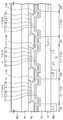
도 4에 도시된 것과 같이, 상기 베이스 기판(SUB) 상에 3번째 주사 라인(S3) 및 상기 i번째 데이터 라인(Di)이 서로 절연되게 배치된다. 또한, 상기 베이스 기판(SUB) 상에 상기 제1 전원전압(ELVDD)을 수신하는 전원라인(KL)이 배치된다. 상기 전원라인(KL)은 상기 i번째 데이터 라인(Di)과 동일한 층상에 배치될 수 있다.As illustrated in FIG. 4, the third scan line S3 and the i-th data line Di are disposed on the base substrate SUB to be insulated from each other. In addition, a power line KL receiving the first power voltage ELVDD is disposed on the base substrate SUB. The power line KL may be disposed on the same layer as the i-th data line Di.
상기 화소(PX(3,i))는 상기 유기발광소자(OLED(3,i))와 회로부(CP)로 구분될 수 있다. 상기 회로부(CP)는 상기 제1 트랜지스터(TFT1), 상기 제2 트랜지스터(TFT2), 및 상기 커패시터(Cap)를 포함한다. 평면상에서 상기 유기발광소자(OLED(3,i))는 상기 화소 정의막(PDL)에 형성된 개구부(OP(3,i))에 중첩한다. 상기 회로부(CP)는 상기 화소 정의막(PDL)에 중첩한다.The pixel PX (3, i) may be divided into the organic light emitting device OLED (3, i) and the circuit unit CP. The circuit part CP includes the first transistor TFT1, the second transistor TFT2, and the capacitor Cap. On the planar surface, the organic light emitting element OLED (3, i) overlaps the opening OP (3, i) formed in the pixel defining layer PDL. The circuit part CP overlaps the pixel defining layer PDL.
도 4 및 도 5에 도시된 것과 같이, 제1 트랜지스터(TFT1)의 제어전극(GE1, 이하 제1 제어전극)은 상기 3번째 주사 라인(S3)으로부터 분기된다. 상기 베이스 기판(SUB) 상에 상기 3번째 주사 라인(S3)을 커버하는 제1 절연층(10)이 배치된다. 상기 제1 절연층(10)은 유기막 및/또는 무기막을 포함한다.4 and 5, the control electrode GE1 (hereinafter, the first control electrode) of the first transistor TFT1 is branched from the third scan line S3. A first insulating
상기 제1 트랜지스터(TFT1)의 반도체층(AL1: 이하, 제1 반도체층)은 상기 제1 절연층(10)을 사이에 두고, 상기 제1 제어전극(GE1) 상에 배치된다. 상기 제1 트랜지스터(TFT1)의 입력전극(SE1: 이하, 제1 입력전극)과 출력전극(DE1: 이하, 제1 출력전극)은 상기 제1 반도체층(AL1)에 중첩하게 배치된다. 상기 제1 입력전극(SE1)과 상기 제1 출력전극(DE1)은 서로 이격되어 배치된다. 도 4 및 도 5는 바텀 게이트 구조의 상기 제1 트랜지스터(TFT1)를 예시적으로 도시하였으나, 이에 제한되지 않고, 상기 제1 트랜지스터(TFT1)는 탑 게이트 구조로 변형되어 실시될 수 있다.The semiconductor layer AL1 (hereinafter, the first semiconductor layer) of the first transistor TFT1 is disposed on the first control electrode GE1 with the first insulating
상기 커패시터(Cap)의 상기 제1 전극(CE1)은 상기 제1 절연층(10) 상에 배치된다. 상기 커패시터(Cap)의 상기 제1 전극(CE1)은 상기 제1 출력전극(DE1)에 연결된다. 상기 제1 절연층(10) 상에 상기 제1 입력전극(SE1), 상기 제1 출력전극(DE1), 및 상기 커패시터(Cap)의 상기 제1 전극(CE1)을 커버하는 제2 절연층(20)이 배치된다. 상기 제2 절연층(20) 상에 상기 커패시터(Cap)의 상기 제2 전극(CE2)이 배치된다. 상기 제2 전극(CE2)은 상기 전원라인(KL)에 연결된다.The first electrode CE1 of the capacitor Cap is disposed on the first insulating
도 4 및 도 6에 도시된 것과 같이, 제2 트랜지스터(TFT2)의 제어전극(GE2: 이하, 제2 제어전극)은 상기 커패시터(Cap)의 제1 전극(CE1)에 연결된다. 상기 제2 트랜지스터(TFT2)의 반도체층(AL2: 이하, 제2 반도체층)은 상기 제1 절연층(10)을 사이에 두고, 상기 제2 제어전극(GE2) 상에 배치된다. 상기 제2 트랜지스터(TFT2)의 입력전극(SE2: 이하, 제2 입력전극)과 출력전극(DE2: 이하, 제2 출력전극)은 상기 제2 반도체층(AL2)에 중첩하게 배치된다. 상기 제2 입력전극(SE2)과 상기 제2 출력전극(DE2)은 서로 이격되어 배치된다. 상기 제2 절연층(20)은 상기 제2 입력전극(SE2) 및 상기 제2 출력전극(DE2)을 커버한다. 도 4 및 도 6에 도시된 것과 달리, 상기 제2 트랜지스터(TFT2)는 탑 게이트 구조로 변형되어 실시될 수 있다.4 and 6, the control electrode GE2 (hereinafter, second control electrode) of the second transistor TFT2 is connected to the first electrode CE1 of the capacitor Cap. The semiconductor layer AL2 (hereinafter, second semiconductor layer) of the second transistor TFT2 is disposed on the second control electrode GE2 with the first insulating
도 5 및 도 6에 도시된 것과 같이, 상기 제2 절연층(20) 상에 상기 유기발광소자(OLED(3,i))가 배치된다. 상기 유기발광소자(OLED(3,i))는 상기 제2 절연층(20) 상에 순차적으로 적층된 제1 전극(AE), 제1 공통층(CHL), 유기발광층(EML), 제2 공통층(CEL), 제2 전극(CE)을 포함한다. 상기 제1 전극(AE)은 상기 제2 절연층(20)을 관통하는 컨택홀(CH1, 도 4 참조)을 통해 상기 제2 출력전극(DE2)에 연결된다.5 and 6, the organic light emitting device OLED (3, i) is disposed on the second insulating
상기 제1 공통층(CHL)은 적어도 정공 주입층을 포함하고, 상기 제2 공통층(CTL)은 적어도 전자 주입층을 포함한다. 상기 제1 공통층(CHL)은 상기 정공 주입층과 상기 유기발광층(EML) 사이에 배치된 정공 수송층을 더 포함하고, 상기 제2 공통층(CEL)은 상기 전자 주입층과 상기 유기발광층(EML) 사이에 배치된 전자 수송층을 더 포함할 수 있다.The first common layer CHL includes at least a hole injection layer, and the second common layer CTL includes at least an electron injection layer. The first common layer CHL further includes a hole transport layer disposed between the hole injection layer and the organic emission layer EML, and the second common layer CEL includes the electron injection layer and the organic emission layer EML. ) May further include an electron transport layer.
상기 베이스 기판(SUB) 상에 상기 유기발광소자(OLED(3,i))를 커버하는 봉지층(ECL)이 배치된다. 상기 봉지층(ECL)은 상기 베이스 기판(SUB) 전체에 배치된다. 예컨대, 상기 봉지층(ECL)은 도 2에 도시된 발광영역들(DA(2,i)~DA(3,i+2)) 및 상기 발광영역들(DA(2,i)~DA(3,i+2))을 에워싸는 비발광영역(NDA)에 모두 중첩한다. 다시말해, 상기 봉지층(ECL)은 상기 발광영역들(DA(2,i)~DA(3,i+2))에 배치된 발광소자들을 모두 커버할 수 있다.An encapsulation layer ECL covering the organic light emitting device OLED (3, i) is disposed on the base substrate SUB. The encapsulation layer ECL is disposed on the entire base substrate SUB. For example, the encapsulation layer ECL includes the light emitting regions DA (2, i) to DA (3, i + 2) and the light emitting regions DA (2, i) to DA (3) shown in FIG. 2. , i + 2)) all overlap the non-emission area NDA. In other words, the encapsulation layer ECL may cover all the light emitting elements disposed in the light emitting areas DA (2, i) to DA (3, i + 2).
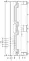
상기 봉지층(ECL) 상에 적어도 하나의 전도성층(CL)과 적어도 하나의 차광층(BM)이 배치된다. 상기 적어도 하나의 전도성층(CL)은 상기 터치패널(TP)의 상기 제1 터치전극들 및/또는 상기 제2 터치전극들을 구성한다. 상기 적어도 하나의 전도성층(CL)은 개구율을 높이기 위해 상기 비발광영역(NDA)에 중첩하게 배치된다.At least one conductive layer CL and at least one light blocking layer BM are disposed on the encapsulation layer ECL. The at least one conductive layer CL constitutes the first touch electrodes and / or the second touch electrodes of the touch panel TP. The at least one conductive layer CL is disposed to overlap the non-emission area NDA to increase the aperture ratio.
상기 적어도 하나의 차광층(BM)은 상기 비발광영역(NDA)에 중첩하게 배치된다. 상기 차광층(BM)은 외부로부터 입사된 광(예컨대, 상기 봉지층(ECL)의 상측으로부터 입사된 광)이 상기 봉지층(ECL)에서 반사되는 것을 방지한다. 상기 차광층(BM)은 상기 외부로부터 입사된 광을 흡수하여 상기 표시장치의 시인성을 향상시킨다.The at least one light blocking layer BM is disposed to overlap the non-emission area NDA. The light blocking layer BM prevents light incident from the outside (eg, light incident from an upper side of the encapsulation layer ECL) from being reflected from the encapsulation layer ECL. The light blocking layer BM absorbs light incident from the outside to improve visibility of the display device.
도 7은 도 2의 K-K'에 대응하는 단면도이다. 도 7은 상기 제1 방향(DR1)으로 배열된 연속하는 3개의 발광영역(DA(2,i)~DA(2,i+2), 이하, 제1 내지 제3 발광영역)의 단면도이다. 도 7은 상기 화소 정의막(PDL) 아래의 구성은 간략하게 도시하였다. 도 7을 참조하여 상기 봉지층(ECL) 상에 배치된 전도성층(CL)과 차광층(BM)에 대해 상세히 설명한다.7 is a cross-sectional view corresponding to K-K 'of FIG. 2. 7 is a cross-sectional view of three consecutive light emitting areas DA (2, i) to DA (2, i + 2), hereinafter referred to as first to third light emitting areas arranged in the first direction DR1. 7 schematically illustrates a configuration under the pixel defining layer PDL. The conductive layer CL and the light blocking layer BM disposed on the encapsulation layer ECL will be described in detail with reference to FIG. 7.
상기 제1 내지 제3 발광영역들(DA(2,i)~DA(2,i+2))에 배치된 유기발광소자들(OLED(2,i)~OLED(2,i+2), 이하 제1 내지 제3 발광소자)은 서로 다른 컬러의 광을 생성할 수 있다. 예컨대, 상기 제1 내지 제3 유기발광소자들(OLED(2,i)~OLED(2,i+2))은 레드 광, 그린 광, 블루 광을 각각 생성할 수 있다.Organic light emitting elements OLED (2, i) to OLED (2, i + 2) disposed in the first to third light emitting regions DA (2, i) to DA (2, i + 2), Hereinafter, the first to third light emitting devices) may generate light having different colors. For example, the first to third organic light emitting elements OLED (2, i) to OLED (2, i + 2) may generate red light, green light, and blue light, respectively.
한편, 상기 표시패널(DP)은 상기 제1 내지 제3 화소들(PX(2,i)~PX(2,i+2)에 인접하게 배치되고, 다른 컬러를 생성하는 제4 화소를 더 포함할 수 있다. 예컨대, 상기 제4 화소는 화이트 광을 생성할 수 있다. 그 밖에 상기 제1 내지 제3 유기발광소자들(OLED(2,i)~OLED(2,i+2))은 화이트 광을 생성할 수도 있다.On the other hand, the display panel DP is disposed adjacent to the first to third pixels PX (2, i) to PX (2, i + 2), and further includes a fourth pixel generating a different color. For example, the fourth pixel may generate white light, and the first to third organic light emitting elements OLED (2, i) to OLED (2, i + 2) may be white. It can also generate light.
상기 전도성층(CL)은 서로 다른 층 상에 배치된 제1 전도성층(CL1)과 제2 전도성층(CL2)을 포함한다. 상기 제1 전도성층(CL1)은 상기 봉지층(ECL) 상에 직접 배치될 수 있다. 상기 제1 전도성층(CL1)은 비발광영역(NDA) 중 일부분에 중첩할 수 있다. 상기 제1 전도성층(CL1)은 상기 제1 터치전극들과 상기 제2 터치전극들 중 어느 하나의 전극들을 이룰 수 있다.The conductive layer CL includes a first conductive layer CL1 and a second conductive layer CL2 disposed on different layers. The first conductive layer CL1 may be directly disposed on the encapsulation layer ECL. The first conductive layer CL1 may overlap a portion of the non-emission area NDA. The first conductive layer CL1 may form any one of the first touch electrodes and the second touch electrodes.
상기 차광층(BM)은 서로 다른 층 상에 배치된 제1 차광층(BM1)과 제2 차광층(BM2)을 포함한다. 상기 제1 차광층(BM1)은 상기 봉지층(ECL) 상에 배치되고, 적어도 상기 제1 전도성층(CL1)을 커버한다. 상기 제1 차광층(BM1)은 상기 제1 전도성층(CL1)으로 입사되는 외부의 광을 흡수한다. 상기 제1 전도성층(CL1)은 상기 비발광영역(NDA) 전체에 배치될 수 있다.The light blocking layer BM includes a first light blocking layer BM1 and a second light blocking layer BM2 disposed on different layers. The first light blocking layer BM1 is disposed on the encapsulation layer ECL, and covers at least the first conductive layer CL1. The first light blocking layer BM1 absorbs external light incident on the first conductive layer CL1. The first conductive layer CL1 may be disposed over the non-emission area NDA.
상기 제1 차광층(BM1) 상에 상기 제2 전도성층(CL2)이 배치된다. 상기 제2 전도성층(CL2)은 상기 제1 터치전극들과 상기 제2 터치전극들 중 다른 하나의 전극들을 이룰 수 있다. 상기 제2 전도성층(CL2)은 상기 비발광영역(NDA) 중 일부분에 중첩할 수 있다. 상기 제2 전도성층(CL2)은 상기 제1 전도성층(CL1)과 중첩하지 않을 수 있다.The second conductive layer CL2 is disposed on the first light blocking layer BM1. The second conductive layer CL2 may form other electrodes of the first touch electrodes and the second touch electrodes. The second conductive layer CL2 may overlap a portion of the non-emission area NDA. The second conductive layer CL2 may not overlap the first conductive layer CL1.
상기 제1 차광층(BM1) 상에 상기 제2 전도성층(CL2)을 커버하는 상기 제2 차광층(BM2)이 배치된다. 상기 제2 차광층(BM2)은 상기 제2 전도성층(CL2)으로 입사되는 외부의 광을 흡수한다. 상기 제2 차광층(BM2)은 상기 비발광영역(NDA) 전체에 중첩할 수 있다. 상기 제2 차광층(BM2)은 상기 제2 전도성층(CL2)에 중첩하면 충분하고 상기 제2 차광층(BM2)의 평면상 형상은 변형될 수 있다.The second light-blocking layer BM2 covering the second conductive layer CL2 is disposed on the first light-blocking layer BM1. The second light blocking layer BM2 absorbs external light incident on the second conductive layer CL2. The second light blocking layer BM2 may overlap the entire non-emission area NDA. The second light-blocking layer BM2 is sufficient to overlap the second conductive layer CL2, and a planar shape of the second light-blocking layer BM2 may be deformed.
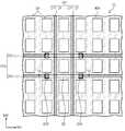
도 8은 본 발명의 일실시예에 따른 터치패널의 평면도이다. 도 8에는 상기 제1 터치전극들(TE1-1~TE1-p)과 상기 제2 터치전극들(TE2-1~TE2-p)만이 도시되었고, 차광층은 생략되었다.8 is a plan view of a touch panel according to an exemplary embodiment of the present invention. In FIG. 8, only the first touch electrodes TE1-1 to TE1-p and the second touch electrodes TE2-1 to TE2-p are illustrated, and the light blocking layer is omitted.
상기 제1 터치전극들(TE1-1~TE1-p)은 상기 제1 방향(DR1)으로 나열된다. 상기 제1 터치전극들(TE1-1~TE1-p) 각각은 상기 제2 방향(DR2)으로 연장된 형상이다. 상기 제2 터치전극들(TE2-1~TE2-q)은 상기 제2 방향(DR2)으로 나열되고 상기 제1 방향(DR1)으로 연장된 형상이다.The first touch electrodes TE1-1 to TE1-p are arranged in the first direction DR1. Each of the first touch electrodes TE1-1 to TE1-p has a shape extending in the second direction DR2. The second touch electrodes TE2-1 to TE2-q are arranged in the second direction DR2 and extend in the first direction DR1.
상기 제1 터치전극들(TE1-1~TE1-p) 각각은 복수 개의 센서부들(SP1, 이하 제1 센서부들)과 복수 개의 연결부들(CP1, 이하 제1 연결부들)를 포함한다. 상기 제1 센서부들(SP1)은 상기 제2 방향(DR2)으로 나열된다. 상기 제1 연결부들(CP1)은 상기 제1 센서부들(SP1)은 중 인접하는 2개의 제1 센서부들을 연결한다.Each of the first touch electrodes TE1-1 to TE1-p includes a plurality of sensor parts SP1 (hereinafter, first sensor parts) and a plurality of connection parts CP1 (hereinafter, first connection parts). The first sensor parts SP1 are arranged in the second direction DR2. The first connection parts CP1 connect two adjacent first sensor parts among the first sensor parts SP1.
상기 제2 터치전극들(TE2-1~TE2-p) 각각은 복수 개의 센서부들(SP2, 이하 제2 센서부들)과 복수 개의 연결부들(CP2, 이하 제2 연결부들)를 포함한다. 상기 제2 센서부들(SP2)은 상기 제2 방향(DR1)으로 나열된다. 상기 제2 연결부들(CP2)은 상기 제2 센서부들(SP2)은 중 인접하는 2개의 제2 센서부들을 연결한다.Each of the second touch electrodes TE2-1 to TE2-p includes a plurality of sensor parts SP2 (hereinafter, second sensor parts) and a plurality of connection parts (CP2, hereinafter second connection parts). The second sensor parts SP2 are arranged in the second direction DR1. The second connection parts CP2 connect two adjacent second sensor parts among the second sensor parts SP2.
상기 제1 센서부들(SP1) 각각은 마름모 형상을 갖고, 상기 제1 연결부들(CP1) 각각은 선 형상이다. 상기 제1 연결부(CP1)들 각각은 상기 인접한 2개의 센서부들의 꼭지점들을 연결한다. 마름모 형상의 상기 제1 센서부들(SP1)은 상기 제1 연결부들(CP1)보다 큰 면적을 갖는다.Each of the first sensor parts SP1 has a rhombus shape, and each of the first connection parts CP1 has a linear shape. Each of the first connection parts CP1 connects vertices of the two adjacent sensor parts. The first sensor parts SP1 having a rhombus shape have a larger area than the first connection parts CP1.
상기 제1 터치전극들(TE1-1~TE1-p)과 상기 제2 터치전극들(TE2-1~TE2-q)은 정전결합된다. 상기 제1 터치전극들(TE1-1~TE1-p)에 스캔신호들(TS-1~TS-p)이 인가됨에 따라 상기 제1 센서부들(SP1)과 상기 제2 센서부들(SP2) 사이에 커패시터들이 형성된다.The first touch electrodes TE1-1 to TE1-p and the second touch electrodes TE2-1 to TE2-q are electrostatically coupled. As the scan signals TS-1 to TS-p are applied to the first touch electrodes TE1-1 to TE1-p, between the first sensor parts SP1 and the second sensor parts SP2 In the capacitors are formed.
상호 커패시턴스(Mutual Capacitance) 방식에 따르면, 상기 제1 터치전극들(TE1-1~TE1-p)은 상기 터치패널 구동부(400, 도 1 참조)로부터 서로 다른 구간에서 활성화되는 상기 스캔신호들(TS-1~TS-p)을 순차적으로 수신할 수 있다. 상기 제2 터치전극들(TE2-1~TE2-q)은 상기 스캔신호들(TS-1~TS-p)로부터 생성된 감지신호들(IS-1~IS-q)을 출력한다.According to a mutual capacitance method, the first touch electrodes TE1-1 to TE1-p are the scan signals TS activated in different sections from the touch panel driver 400 (see FIG. 1). -1 to TS-p) can be sequentially received. The second touch electrodes TE2-1 to TE2-q output sensing signals IS-1 to IS-q generated from the scan signals TS-1 to TS-p.
상기 제1 터치전극들(TE1-1~TE1-p) 중 3번째 터치전극(TE1-3)과 상기 제2 터치전극들(TE2-1~TE2-q) 중 3번째 터치전극(TE2-3)이 교차하는 영역을 상기 입력지점(PP)으로 가정한다. 여기서, 상기 입력지점(PP)은 사용자의 손가락과 같은 입력수단에 의해 발생한다.The third touch electrode TE1-3 of the first touch electrodes TE1-1 to TE1-p and the third touch electrode TE2-3 of the second touch electrodes TE2-1 to TE2-q ) Is assumed to be the input point (PP). Here, the input point PP is generated by an input means such as a user's finger.
상기 제2 터치전극들(TE2-1~TE2-q) 중 3번째 터치전극(TE2-3)으로부터 출력된 감지신호(IS-3)는 나머지 상기 제2 터치전극들(TE-1, TE-2, TE-3~TE-q)로부터 출력된 감지신호들(IS-1, IS-2, IS-4~IS-q)과 다른 레벨을 갖는다. The detection signal IS-3 output from the third touch electrode TE2-3 among the second touch electrodes TE2-1 to TE2-q is the rest of the second touch electrodes TE-1 and TE-. 2, it has a different level from the detection signals (IS-1, IS-2, IS-4 to IS-q) output from TE-3 to TE-q.
상기 좌표 산출부(500, 도 1 참조)는 상기 레벨이 다른 감지신호(IS-3)가 검출된 시간에 따라 상기 입력지점(PP)의 상기 제1 방향(DR1)의 좌표정보를 산출하고, 상기 3번째 터치전극(TE2-3)의 상기 제2 터치전극들(TE2-1~TE2-q)에 대한 상대적 위치에 근거하여, 상기 입력지점(PP)의 상기 제2 방향(DR2)의 좌표정보를 산출할 수 있다.The coordinate calculating unit 500 (refer to FIG. 1) calculates coordinate information of the first direction DR1 of the input point PP according to the time at which the detection signal IS-3 having the different level is detected, Coordinates of the second direction DR2 of the input point PP based on the relative position of the third touch electrode TE2-3 to the second touch electrodes TE2-1 to TE2-q. Information can be calculated.
상기 좌표 산출부(500)는 증폭기, 노이즈 필터, 및 아날로그-디지털 컨버터 등을 포함한다. 상기 증폭기는 대응하는 상기 감지신호들(IS-1~IS-q)을 증폭시킨다. 상기 노이즈 필터는 상기 증폭된 상기 감지신호들(IS-1~IS-q)의 노이즈를 제거한다. 상기 아날로그-디지털 컨버터는 상기 노이즈가 제거된 상기 감지신호들(IS-1~IS-q)을 디지털 신호들로 변환한다. 상기 디지털 신호들로부터 상기 입력지점(PP)의 좌표정보를 산출할 수 있다.The coordinate
상기 제1 터치전극들(TE1-1~TE1-p)과 상기 제2 터치전극들(TE2-1~TE2-p)은 서로 다른 층 상에 배치될 수 있다. 상기 제1 터치전극들(TE1-1~TE1-p)은 도 7에 도시된 제1 전도성층(CL1)으로부터 형성될 수 있다. 상기 제2 터치전극들(TE2-1~TE2-p)은 도 7에 도시된 제2 전도성층(CL2)으로부터 형성될 수 있다. 결과적으로 상기 제1 터치전극들(TE1-1~TE1-p)과 상기 제2 터치전극들(TE2-1~TE2-p)은 상기 제1 차광층(BM1)을 사이에 두고 서로 다른 층 상에 배치된다. 이하, 도 10 내지 도 15를 참조하여 상기 제1 터치전극들(TE1-1~TE1-p)과 상기 제2 터치전극들(TE2-1~TE2-p)에 대해 좀 더 상세히 설명한다.The first touch electrodes TE1-1 to TE1-p and the second touch electrodes TE2-1 to TE2-p may be disposed on different layers. The first touch electrodes TE1-1 to TE1-p may be formed from the first conductive layer CL1 illustrated in FIG. 7. The second touch electrodes TE2-1 to TE2-p may be formed from the second conductive layer CL2 illustrated in FIG. 7. As a result, the first touch electrodes TE1-1 to TE1-p and the second touch electrodes TE2-1 to TE2-p are on different layers with the first light blocking layer BM1 therebetween. Is placed on. Hereinafter, the first touch electrodes TE1-1 to TE1-p and the second touch electrodes TE2-1 to TE2-p will be described in more detail with reference to FIGS. 10 to 15.
도 9는 도 8의 일부분을 확대한 평면도이다. 도 10은 도 8의 AA 부분을 확대한 평면도이다. 도 11은 도 10의 Ⅲ-Ⅲ'에 대응하는 단면도이다. 도 10은 상기 제1 센서부들(SP1) 중 어느 하나의 제1 센서부의 일부분을 확대하여 도시하였다.9 is an enlarged plan view of a portion of FIG. 8. 10 is an enlarged plan view of portion AA of FIG. 8. 11 is a cross-sectional view corresponding to III-III 'of FIG. 10. FIG. 10 is an enlarged view of a portion of the first sensor unit of any one of the first sensor units SP1.
도 10에 도시된 것과 같이, 상기 제1 센서부(SP1)는 상기 대응하는 발광영역들(DA)에 인접한 비발광영역(NDA)에 중첩한다. 상기 제1 센서부(SP1)는 상기 제1 방향(DR1)으로 연장된 복수 개의 제1 가로부들(SP1-L)과 상기 제2 방향(DR2)으로 연장된 복수 개의 제1 세로부들(SP1-C)을 포함한다.As illustrated in FIG. 10, the first sensor part SP1 overlaps the non-emission area NDA adjacent to the corresponding emission areas DA. The first sensor part SP1 includes a plurality of first horizontal parts SP1-L extending in the first direction DR1 and a plurality of first vertical parts SP1- extending in the second direction DR2. C).
상기 복수 개의 제1 가로부들(SP1-L)과 상기 복수 개의 제1 세로부들(SP1-C)은 서로 연결되어 복수 개의 개구부들(SP1-OP)을 형성한다. 다시 말해, 상기 제1 센서부(SP1)는 상기 복수 개의 개구부들(SP1-OP)을 구비한 메쉬형상을 갖는다. 상기 제1 센서부(SP1)는 ITO와 같은 투명한 도전성 물질을 포함하거나, 구리, 알루미늄과 같은 금속을 포함할 수 있다.The plurality of first horizontal portions SP1-L and the plurality of first vertical portions SP1-C are connected to each other to form a plurality of openings SP1-OP. In other words, the first sensor part SP1 has a mesh shape having the plurality of openings SP1-OP. The first sensor part SP1 may include a transparent conductive material such as ITO, or a metal such as copper or aluminum.
도 11에 도시된 것과 같이, 상기 제1 센서부(SP1)는 상기 제1 차광층(BM1)에 의해 커버된다. 상기 제1 센서부(SP1)에 중첩하는 상기 제1 차광층(BM1) 상에 상기 제2 차광층(BM2)이 배치된다.11, the first sensor part SP1 is covered by the first light blocking layer BM1. The second light blocking layer BM2 is disposed on the first light blocking layer BM1 overlapping the first sensor part SP1.
도 12는 도 8의 BB 부분을 확대한 평면도이다. 도 13은 도 10의 Ⅳ-Ⅳ'에 대응하는 단면도이다. 도 12에 도시된 것과 같이, 상기 제2 센서부(SP2)는 상기 대응하는 발광영역들(DA)에 인접한 비발광영역(NDA)에 중첩한다. 상기 제2 센서부(SP2)는 복수 개의 제2 가로부들(SP2-L)과 복수 개의 제2 세로부들(SP2-C)을 포함한다. 상기 복수 개의 제2 가로부들(SP2-L)과 상기 복수 개의 제2 세로부들(SP2-C)은 서로 연결되어 복수 개의 개구부들(SP2-OP)을 형성한다.12 is an enlarged plan view of a portion BB of FIG. 8. 13 is a cross-sectional view corresponding to IV-IV 'of FIG. 10. 12, the second sensor part SP2 overlaps the non-emission area NDA adjacent to the corresponding emission areas DA. The second sensor part SP2 includes a plurality of second horizontal parts SP2-L and a plurality of second vertical parts SP2-C. The plurality of second horizontal parts SP2-L and the plurality of second vertical parts SP2-C are connected to each other to form a plurality of openings SP2-OP.
다시 말해, 상기 제2 센서부(SP2)는 상기 복수 개의 개구부들(SP2-OP)을 구비한 메쉬형상을 갖는다. 상기 제2 센서부(SP2)는 ITO와 같은 투명한 도전성 물질을 포함하거나, 구리, 알루미늄과 같은 금속을 포함할 수 있다.In other words, the second sensor part SP2 has a mesh shape having the plurality of openings SP2-OP. The second sensor part SP2 may include a transparent conductive material such as ITO, or a metal such as copper or aluminum.
도 12에 도시된 것과 같이, 상기 제2 센서부(SP2)는 상기 제1 차광층(BM1) 상에 배치된다. 상기 제2 센서부(SP2)는 상기 제1 차광층(BM1) 상에 배치된 상기 제2 차광층(BM2)에 의해 커버된다.As illustrated in FIG. 12, the second sensor part SP2 is disposed on the first light blocking layer BM1. The second sensor part SP2 is covered by the second light blocking layer BM2 disposed on the first light blocking layer BM1.
도 14는 도 8의 CC 부분을 확대한 평면도이다. 도 15는 도 14의 Ⅴ-Ⅴ'에 대응하는 단면도이다.14 is an enlarged plan view of a portion CC of FIG. 8. 15 is a cross-sectional view corresponding to V-V 'of FIG. 14.
도 14 및 도 15에 도시된 것과 같이, 상기 제1 연결부(CP1)는 상기 봉지층(ECL) 상에 배치된 2개의 세로부들(CP1-C1, CP1-C2)를 포함할 수 있다. 상기 제2 연결부(CP2)는 상기 제1 차광층(BM1) 상에 배치된 2개의 가로부들(CP2-L1, CP2-L2)를 포함할 수 있다. 상기 제1 연결부(CP1)는 상기 제1 센서부(SP1)와 동일한 물질로 구성되고, 상기 제2 연결부(CP2)는 상기 제2 센서부(SP2)와 동일한 물질로 구성된다. 별도로 도시하지 않았으나, 상기 제1 연결부(CP1)는 상기 비발광영역(NDA)에 중첩하고 상기 2개의 세로부들(CP1-C1, CP1-C2)을 연결하는 가로부들을 더 포함할 수 있다. 즉, 상기 제1 연결부(CP1)는 메쉬구조를 가질 수 있다. 상기 제2 연결부(CP2) 또한 메쉬구조를 가질 수 있다.14 and 15, the first connection portion CP1 may include two vertical portions CP1-C1 and CP1-C2 disposed on the encapsulation layer ECL. The second connection part CP2 may include two horizontal parts CP2-L1 and CP2-L2 disposed on the first light blocking layer BM1. The first connection part CP1 is made of the same material as the first sensor part SP1, and the second connection part CP2 is made of the same material as the second sensor part SP2. Although not separately illustrated, the first connection part CP1 may further include horizontal parts overlapping the non-emission area NDA and connecting the two vertical parts CP1-C1 and CP1-C2. That is, the first connection portion CP1 may have a mesh structure. The second connection part CP2 may also have a mesh structure.
도 16은 본 발명의 일 실시예에 따른 제1 터치전극의 단면도이고, 도 17은 본 발명의 일 실시예에 따른 제2 터치전극의 단면도이다. 도 16 및 도 17은 도 11 및 도 13에 각각 대응한다.16 is a cross-sectional view of a first touch electrode according to an embodiment of the present invention, and FIG. 17 is a cross-sectional view of a second touch electrode according to an embodiment of the present invention. 16 and 17 correspond to FIGS. 11 and 13, respectively.
본 실시예에 따르면, 상기 제1 터치전극들(TE1-1~TE1-p)과 상기 제2 터치전극들(TE2-1~TE2-p)은 부분적으로 서로 동일한 층 상에 배치될 수 있다. 상기 제2 터치전극들(TE2-1~TE2-p)의 상기 제2 센서부들(SP2)은 상기 제1 터치전극들(TE1-1~TE1-p)과 동일한 층 상에 배치될 수 있다.According to this embodiment, the first touch electrodes TE1-1 to TE1-p and the second touch electrodes TE2-1 to TE2-p may be partially disposed on the same layer. The second sensor parts SP2 of the second touch electrodes TE2-1 to TE2-p may be disposed on the same layer as the first touch electrodes TE1-1 to TE1-p.
이때, 상기 제1 터치전극들(TE1-1~TE1-p)과 상기 제2 센서부들(SP2)은 도 7에 도시된 제1 전도성층(CL1)으로부터 형성될 수 있다. 상기 제2 터치전극들(TE2-1~TE2-p)의 상기 제2 연결부들(CP2)은 도 7에 도시된 제2 전도성층(CL2)으로부터 형성될 수 있다.In this case, the first touch electrodes TE1-1 to TE1-p and the second sensor parts SP2 may be formed from the first conductive layer CL1 illustrated in FIG. 7. The second connection portions CP2 of the second touch electrodes TE2-1 to TE2-p may be formed from the second conductive layer CL2 illustrated in FIG. 7.
도 16 및 도 17에 도시된 것과 같이, 상기 제1 센서부(SP1)의 제1 가로부(SP1-L)와 상기 제2 센서부(SP2)의 제2 세로부(SP2-C)가 상기 봉지층(ECL) 상에 배치된다. 상기 제1 가로부(SP1-L)와 상기 제2 세로부(SP2-C)는 상기 제1 차광층(BM1)에의해 커버된다.16 and 17, the first horizontal portion SP1-L of the first sensor portion SP1 and the second vertical portion SP2-C of the second sensor portion SP2 are the It is disposed on the encapsulation layer (ECL). The first horizontal portion SP1-L and the second vertical portion SP2-C are covered by the first light blocking layer BM1.
도 18은 본 발명의 일 실시예에 따른 제1 터치전극과 제2 터치전극의 교차 부분을 확대한 평면도이다. 도 19는 도 18의 Ⅵ-Ⅵ'에 대응하는 단면도이다.18 is an enlarged plan view of an intersection of a first touch electrode and a second touch electrode according to an embodiment of the present invention. 19 is a cross-sectional view corresponding to VI-VI 'of FIG. 18.
상기 제1 연결부(CP1)는 상기 봉지층(ECL) 상에 배치된 2개의 세로부들(CP1-C1, CP1-C2)를 포함할 수 있다. 상기 제2 연결부(CP2)는 상기 봉지층(ECL) 상에 배치된 2개의 가로부들(CP2-L1, CP2-L2)를 포함할 수 있다. 상기 봉지층(ECL) 상에 상기 제1 연결부(CP1)를 커버하는 상기 제1 차광층(BM1)이 배치된다. 상기 제1 차광층(BM1)은 상기 제2 연결부(CP2)도 부분적으로 커버한다.The first connection portion CP1 may include two vertical portions CP1-C1 and CP1-C2 disposed on the encapsulation layer ECL. The second connection portion CP2 may include two horizontal portions CP2-L1 and CP2-L2 disposed on the encapsulation layer ECL. The first light blocking layer BM1 covering the first connection part CP1 is disposed on the encapsulation layer ECL. The first light blocking layer BM1 partially covers the second connection part CP2.
상기 제2 연결부(CP2)는 상기 제1 차광층(BM1) 상에 배치된 브릿지(BE)를 포함한다. 상기 봉지층(ECL) 상에서 상기 제2 연결부(CP2)는 상기 제1 연결부(CP1)과 교차하는 영역에서 단선된다. 상기 브릿지(BE)는 상기 제1 차광층(BM1)을 관통하는 제2 컨택홀(CH2)과 상기 제3 컨택홀(CH3)을 통해 상기 제2 연결부(CP2)의 단선된 부분을 연결한다.The second connection part CP2 includes a bridge BE disposed on the first light blocking layer BM1. On the encapsulation layer ECL, the second connection part CP2 is disconnected in an area crossing the first connection part CP1. The bridge BE connects the disconnected portion of the second connection part CP2 through the second contact hole CH2 penetrating the first light blocking layer BM1 and the third contact hole CH3.
본 발명의 다른 실시예에서 상기 제2 연결부(CP2) 및 상기 제2 연결부(CP2)가 상기 제1 차광층(BM1) 상에 배치되고, 상기 브릿지(BE)가 상기 봉지층(ECL) 상에 배치될 수도 있다.In another embodiment of the present invention, the second connection portion CP2 and the second connection portion CP2 are disposed on the first light blocking layer BM1, and the bridge BE is on the encapsulation layer ECL. It may be deployed.
한편, 도 16 내지 도 18에 도시된 것과 같이, 동일한 층 상에 배치된 상기 제1 센서부들(SP1)과 상기 제2 센서부들(SP2)을 포함하는 정전용량식 터치패널은 자기 커패시턴스(Self Capacitance) 방식으로 상기 입력지점의 좌표정보를 산출할 수 있다.Meanwhile, as illustrated in FIGS. 16 to 18, the capacitive touch panel including the first sensor parts SP1 and the second sensor parts SP2 disposed on the same layer has a self-capacitance. ) Method to calculate the coordinate information of the input point.
도 20a 및 도 20b는 본 발명의 일실시예에 따른 터치패널의 평면도들이다. 도 20a와 같이 정전용량식 터치패널의 제1 터치전극들과 제2 터치전극들의 형상은 변형될 수 있다. 상기 제1 터치전극들(TE10-1~TE10-p)과 상기 제2 터치전극들(TE20-1~TE20-q)은 서로 교차하는 바 형상을 가질 수 있다. 상기 제1 터치전극들(TE10-1~TE10-p)과 상기 제2 터치전극들(TE20-1~TE20-q)은 서로 다른 층 상에 배치되거나, 부분적으로 서로 다른 층 상에 배치될 수도 있다. 상기 제1 터치전극들(TE10-1~TE10-p)과 상기 제2 터치전극들(TE20-1~TE20-q)은 서로 교차하는 영역에서 서로 다른 층 상에 배치될 수도 있다.20A and 20B are plan views of a touch panel according to an exemplary embodiment of the present invention. As shown in FIG. 20A, shapes of the first touch electrodes and the second touch electrodes of the capacitive touch panel may be modified. The first touch electrodes TE10-1 to TE10-p and the second touch electrodes TE20-1 to TE20-q may have a bar shape intersecting each other. The first touch electrodes TE10-1 to TE10-p and the second touch electrodes TE20-1 to TE20-q may be disposed on different layers or may be partially disposed on different layers. have. The first touch electrodes TE10-1 to TE10-p and the second touch electrodes TE20-1 to TE20-q may be disposed on different layers in regions intersecting each other.
도 20b에 도시된 것과 같이, 상기 터치패널은 전자기 유도방식의 터치패널일 수 있다. 상기 전자기 유도방식의 터치패널은 서로 교차하는 제1 터치코일들(TE100-1~TE100-p)과 제2 터치코일들(TE200-1~TE200-q)을 포함한다. 상기 제1 터치코일들(TE100-1~TE100-p)과 상기 제2 터치코일들(TE200-1~TE200-q)은 서로 다른 층 상에 배치되거나, 부분적으로 서로 다른층 상에 배치될 수도 있다. 상기 제1 터치코일들(TE100-1~TE100-p)과 상기 제2 터치코일들(TE200-1~TE200-q)은 서로 교차하는 영역에서 서로 다른 층 상에 배치될 수도 있다.20B, the touch panel may be an electromagnetic induction type touch panel. The electromagnetic induction type touch panel includes first touch coils (TE100-1 to TE100-p) and second touch coils (TE200-1 to TE200-q) that cross each other. The first touch coils TE100-1 to TE100-p and the second touch coils TE200-1 to TE200-q may be disposed on different layers, or may be partially disposed on different layers. have. The first touch coils TE100-1 to TE100-p and the second touch coils TE200-1 to TE200-q may be disposed on different layers in regions intersecting each other.
도 21은 본 발명의 일 실시예에 따른 유기발광 표시장치의 일부분의 단면도이다. 도 21은 도 7에 대응하는 단면을 도시하였다. 이하, 도 21을 참조하여 본 실시예에 따른 유기발광 표시장치를 설명한다. 다만, 도 1 내지 도 20을 참조하여 설명한 구성과 중복되는 구성에 대한 상세한 설명은 생략한다.21 is a cross-sectional view of a portion of an organic light emitting display device according to an exemplary embodiment of the present invention. FIG. 21 shows a cross section corresponding to FIG. 7. Hereinafter, an organic light emitting display device according to the present embodiment will be described with reference to FIG. 21. However, detailed descriptions of the components overlapping with those described with reference to FIGS. 1 to 20 will be omitted.
도 21에 도시된 것과 같이, 상기 전도성층(CL-1)은 서로 다른 층 상에 배치된 제1 전도성층(CL10)과 제2 전도성층(CL2)을 포함한다. 상기 제1 전도성층(CL10)은 비발광영역(NDA)에 중첩한다. 상기 제1 전도성층(CL10)은 상기 제1 터치전극들(TE1-1~TE1-p, 도 8 참조)과 상기 제2 터치전극들(TE2-1~TE2-q, 도 8 참조) 중 적어도 어느 하나의 전극들을 이룰 수 있다.As shown in FIG. 21, the conductive layer CL-1 includes a first conductive layer CL10 and a second conductive layer CL2 disposed on different layers. The first conductive layer CL10 overlaps the non-emission area NDA. The first conductive layer CL10 includes at least one of the first touch electrodes TE1-1 to TE1-p (see FIG. 8) and the second touch electrodes (TE2-1 to TE2-q, see FIG. 8). Either electrode can be achieved.
상기 제1 전도성층(CL10)은 전도성 차광물질을 포함한다. 상기 전도성 차광물질은 반사율이 낮은 전도성 물질을 포함한다. 예컨대, 상기 전도성 차광물질은 크롬 산화물(Chromium oxide), 크롬 질화물(Chromium nitride), 티타늄 산화물(Titanium oxide), 및 티타늄 질화물(Titanium nitride) 중 어느 하나 또는 이들의 합금 등을 포함한다.The first conductive layer CL10 includes a conductive light blocking material. The conductive light-shielding material includes a conductive material having low reflectance. For example, the conductive light-shielding material includes any one of chromium oxide, chromium nitride, titanium oxide, and titanium nitride, or alloys thereof.
상기 봉지층 상에 상기 제1 전도성층(CL10)을 커버하는 제3 절연층(30)이 배치된다. 상기 제3 절연층(30)은 광을 투과시키는 투명한 절연물질을 포함한다. 상기 제3 절연층(30)은 상기 비발광영역(NDA)뿐만 아니라, 상기 발광영역들(DA(2,i), DA(2,i+1), DA(2,i+2))에도 중첩할 수 있다.A third insulating
본 실시예에 따르면, 도 7에 도시된 제1 차광층(BM1)이 생략될 수 있다. 상기 제3 절연층(30)은 패터닝이 불필요하므로, 미스 얼라인 문제가 발생하지 않는다.According to this embodiment, the first light blocking layer BM1 shown in FIG. 7 may be omitted. Since the third insulating
상기 제3 절연층(30) 상에 상기 비발광영역(NDA)에 중첩하는 상기 제2 전도성층(CL2)이 배치된다. 상기 제2 전도성층(CL2)은 상기 제1 전도성층(CL10)과 다른 전도성 반사물질, 예컨대, 구리, 알루미늄과 같은 금속을 포함할 수 있다. 상기 제2 전도성층(CL2)은 도 13에 도시된 것과 같이 제2 센서부(SP2)를 이루거나, 도 19에 도시된 것과 같이 브릿지(BE)를 구성할 수 있다.The second conductive layer CL2 overlapping the non-emission region NDA is disposed on the third insulating
상기 제3 절연층(30) 상에 상기 제2 전도성층(CL2)을 커버하는 상기 제2 차광층(BM2)이 배치된다. 상기 제2 차광층(BM2) 역시 상기 비발광영역(NDA)에 중첩한다.The second light blocking layer BM2 covering the second conductive layer CL2 is disposed on the third insulating
본 발명의 다른 실시예에서, 상기 제2 전도성층(CL2)은 상기 전도성 차광물질을 포함할 수 있다. 이때, 상기 제2 차광층(BM2)은 생략될 수 있다.In another embodiment of the present invention, the second conductive layer CL2 may include the conductive light blocking material. In this case, the second light blocking layer BM2 may be omitted.
이상에서는 본 발명의 바람직한 실시예를 참조하여 설명하였지만, 해당 기술 분야의 숙련된 당업자 또는 해당 기술 분야에 통상의 지식을 갖는 자라면, 후술될 특허청구범위에 기재된 본 발명의 사상 및 기술 영역으로부터 벗어나지 않는 범위 내에서 본 발명을 다양하게 수정 및 변경시킬 수 있음을 이해할 수 있을 것이다.In the above, it has been described with reference to preferred embodiments of the present invention, but those skilled in the art or those of ordinary skill in the art will depart from the spirit and technical scope of the present invention as set forth in the claims below. It will be understood that various modifications and changes may be made to the present invention without departing from the scope.
따라서, 본 발명의 기술적 범위는 명세서의 상세한 설명에 기재된 내용으로 한정되는 것이 아니라 특허청구범위에 의해 정하여져야만 할 것이다.Therefore, the technical scope of the present invention should not be limited to the contents described in the detailed description of the specification, but should be defined by the claims.
DP: 유기발광 표시패널TP: 터치패널
DA: 발광영역NDA: 비발광영역
BM1, BM2: 차광층TE1-1~TE1-p: 제1 터치전극
TE2-1~TE2-q: 제2 터치전극DP: organic light emitting display panel TP: touch panel
DA: Emission area NDA: Non-emission area
BM1, BM2: Light-shielding layers TE1-1 to TE1-p: first touch electrodes
TE2-1 ~ TE2-q: Second touch electrode
Claims (18)
Translated fromKorean제1 터치전극들, 및 상기 제1 터치전극들과 교차하는 제2 터치전극들을 포함하고, 상기 제1 터치전극들과 상기 제2 터치전극들은 상기 봉지층 상에 상기 비발광영역에 중첩하게 배치된 터치패널을 포함하고,
상기 제1 터치전극들과 상기 제2 터치전극들은 상기 제1 차광층을 사이에 두고 서로 이격되는 유기발광 표시장치.A base substrate divided into light emitting regions and a non-light emitting region adjacent to the light emitting regions, organic light emitting elements disposed corresponding to the light emitting regions, an encapsulation layer covering the organic light emitting elements, and on the encapsulation layer An organic light emitting display panel including a first light blocking layer disposed to overlap the non-light emitting area; And
First touch electrodes, and second touch electrodes intersecting the first touch electrodes, wherein the first touch electrodes and the second touch electrodes are disposed to overlap the non-emission region on the encapsulation layer. It includes a touch panel,
The first touch electrodes and the second touch electrodes are organic light emitting display devices spaced apart from each other with the first light blocking layer therebetween.
상기 제1 터치전극들과 상기 제2 터치전극들은 상기 제1 차광층을 사이에 두고 서로 다른 층 상에 배치된 것을 특징으로 하는 유기발광 표시장치.According to claim 1,
The first touch electrodes and the second touch electrodes are disposed on different layers with the first light-blocking layer interposed therebetween.
상기 제1 터치전극들과 상기 제2 터치전극들 각각은, 상기 발광영역들 중 대응하는 발광영역들에 중첩하는 개구부들을 포함하는 것을 특징으로 하는 유기발광 표시장치.According to claim 2,
Each of the first touch electrodes and the second touch electrodes includes openings overlapping corresponding light emitting areas among the light emitting areas.
상기 제1 차광층 상에 배치되고, 상기 제1 터치전극들과 상기 제2 터치전극들 중 상기 제1 차광층 상에 배치된 터치전극들을 커버하는 제2 차광층을 더 포함하는 유기발광 표시장치.According to claim 2,
An organic light emitting display device further comprising a second light blocking layer disposed on the first light blocking layer and covering touch electrodes disposed on the first light blocking layer among the first touch electrodes and the second touch electrodes. .
상기 제1 터치전극들은 제1 방향으로 연장되고 상기 제1 방향에 교차하는 제2 방향으로 나열되며, 상기 제2 터치전극들은 상기 제2 방향으로 연장되고 상기 제1 방향으로 나열된 것을 특징으로 하는 유기발광 표시장치.According to claim 1,
The first touch electrodes are arranged in a second direction extending in a first direction and crossing the first direction, and the second touch electrodes are extended in the second direction and arranged in the first direction. Light emitting display.
상기 제1 터치전극들 각각은, 상기 제1 방향으로 나열된 제1 센서부들 및 상기 제1 센서부들 중 인접하는 2개의 제1 센서부들을 연결하는 제1 연결부들을 포함하고,
상기 제2 터치전극들 각각은, 상기 제2 방향으로 나열된 제2 센서부들 및 상기 제1 연결부들과 절연되게 교차하며 상기 제2 센서부들 중 인접하는 2개의 제2 센서부들을 연결하는 제2 연결부들을 포함하는 유기발광 표시장치.The method of claim 5,
Each of the first touch electrodes includes first sensor units arranged in the first direction and first connection units connecting two adjacent first sensor units among the first sensor units,
Each of the second touch electrodes is insulated from the second sensor parts arranged in the second direction and the first connection parts, and a second connection part connecting two adjacent second sensor parts among the second sensor parts. Organic light emitting display device comprising a.
상기 제1 센서부들과 상기 제2 센서부들은 동일한 층 상에 배치되고,
상기 제1 연결부들과 상기 제2 연결부들은 다른 층 상에 배치되어 절연되게 교차하는 것을 특징으로 하는 유기발광 표시장치.The method of claim 6,
The first sensor parts and the second sensor parts are disposed on the same layer,
The first connection portion and the second connection portion is disposed on a different layer, characterized in that the organic light emitting display intersects.
상기 제1 센서부들과 상기 제2 센서부들은 상기 제1 차광층에 의해 커버된 것을 특징으로 하는 유기발광 표시장치.The method of claim 7,
The first sensor portion and the second sensor portion is an organic light emitting display device, characterized in that covered by the first light-shielding layer.
상기 제1 연결부들은 상기 제1 센서부들과 동일한 층 상에 배치되고,
상기 제2 연결부들 각각은 상기 제1 차광층을 관통하는 컨택홀들을 통해서 상기 인접하는 2개의 제2 센서부들을 연결하는 것을 특징으로 하는 유기발광 표시장치.The method of claim 8,
The first connection parts are disposed on the same layer as the first sensor parts,
Each of the second connection parts connects the two adjacent second sensor parts through contact holes penetrating the first light-shielding layer.
상기 제1 차광층 상에 배치되고, 적어도 상기 제1 연결부들과 상기 제2 연결부들을 중 상기 제1 차광층으로부터 노출된 연결부들을 커버하는 제2 차광층을 더 포함하는 유기발광 표시장치.The method of claim 8,
And a second light blocking layer disposed on the first light blocking layer, the second light blocking layer covering at least the first connection parts and the second connection parts, which are exposed from the first light blocking layer.
제1 터치전극들, 및 상기 제1 터치전극들과 교차하는 제2 터치전극들을 포함하고, 상기 제1 터치전극들과 상기 제2 터치전극들은 상기 봉지층 상에 상기 비발광영역에 중첩하게 배치된 터치패널을 포함하고,
상기 제1 터치전극들 및 상기 제2 터치전극들 중 적어도 어느 하나의 전극들은 전도성 차광물질을 포함하고,
상기 제1 터치전극들과 상기 제2 터치전극들은 상기 봉지층 상에 배치된 절연층을 사이에 두고 서로 이격되는 것을 특징으로 하는 유기발광 표시장치.An organic light emitting display panel comprising a base substrate divided into light emitting areas and a non-light emitting area adjacent to the light emitting areas, organic light emitting elements disposed corresponding to the light emitting areas, and an encapsulation layer covering the organic light emitting devices. ; And
First touch electrodes, and second touch electrodes intersecting the first touch electrodes, wherein the first touch electrodes and the second touch electrodes are disposed to overlap the non-emission region on the encapsulation layer. It includes a touch panel,
At least one of the first touch electrodes and the second touch electrodes includes a conductive light blocking material,
And the first touch electrodes and the second touch electrodes are spaced apart from each other with an insulating layer disposed on the encapsulation layer interposed therebetween.
상기 전도성 차광물질은 크롬 산화물(Chromium oxide), 크롬 질화물(Chromium nitride), 티타늄 산화물(Titanium oxide), 및 티타늄 질화물(Titanium nitride) 중 어느 하나 또는 이들의 합금 등을 포함하는 것을 특징으로 하는 유기발광 표시장치.The method of claim 11,
The conductive light-shielding material is chromium oxide (Chromium oxide), chromium nitride (Chromium nitride), titanium oxide (Titanium oxide), and any one of the titanium nitride (Titanium nitride) or an organic light emitting, characterized in that it comprises an alloy thereof Display device.
상기 제1 터치전극들과 상기 제2 터치전극들은 상기 절연층을 사이에 두고 서로 다른 층 상에 배치된 것을 특징으로 하는 유기발광 표시장치.The method of claim 11,
The first touch electrodes and the second touch electrodes are disposed on different layers with the insulating layer interposed therebetween.
상기 제1 터치전극들은 상기 전도성 차광물질을 포함하고, 상기 제2 터치전극들은 전도성 반사물질을 포함하며,
상기 절연층 상에 배치되고, 상기 제2 터치전극들을 커버하며, 절연성 차광물질을 포함하는 차광층을 더 포함하는 유기발광 표시장치.The method of claim 13,
The first touch electrodes include the conductive light blocking material, and the second touch electrodes include a conductive reflective material,
An organic light emitting display device disposed on the insulating layer, covering the second touch electrodes, and further comprising a light blocking layer including an insulating light blocking material.
상기 제1 터치전극들 및 상기 제2 터치전극들은 상기 전도성 차광물질을 포함하는 유기발광 표시장치.The method of claim 11,
The first touch electrodes and the second touch electrodes are organic light emitting display devices including the conductive light blocking material.
상기 제1 터치전극들 각각은, 제1 방향으로 나열된 제1 센서부들 및 상기 제1 센서부들 중 인접하는 2개의 제1 센서부들을 연결하는 제1 연결부들을 포함하고,
상기 제2 터치전극들 각각은, 상기 제1 방향과 교차하는 제2 방향으로 나열된 제2 센서부들 및 절연층을 사이에 두고 상기 제1 연결부들과 교차하며 상기 제2 센서부들 중 인접하는 2개의 제2 센서부들을 연결하는 제2 연결부들을 포함하는 유기발광 표시장치.The method of claim 15,
Each of the first touch electrodes includes first sensor units arranged in a first direction and first connection units connecting two adjacent first sensor units among the first sensor units,
Each of the second touch electrodes crosses the first connection parts with the second sensor parts arranged in a second direction intersecting the first direction and an insulating layer interposed therebetween, and adjacent two of the second sensor parts. An organic light emitting display device including second connection parts connecting second sensor parts.
상기 제1 센서부들과 상기 제2 센서부들은 동일한 층 상에 배치되고,
상기 제1 연결부들과 상기 제2 연결부들은 다른 층 상에 배치되어 절연되게 교차하는 것을 특징으로 하는 유기발광 표시장치.The method of claim 16,
The first sensor parts and the second sensor parts are disposed on the same layer,
The first connection portion and the second connection portion is disposed on a different layer, characterized in that the organic light emitting display intersects.
상기 제1 연결부들은 상기 제1 센서부들과 동일한 층 상에 배치되고,
상기 제2 연결부들 각각은 상기 절연층을 관통하는 컨택홀들을 통해서 상기 인접하는 2개의 제2 센서부들을 연결하는 것을 특징으로 하는 유기발광 표시장치.
The method of claim 17,
The first connection parts are disposed on the same layer as the first sensor parts,
Each of the second connecting portions connects the two adjacent second sensor portions through contact holes penetrating the insulating layer.
Priority Applications (2)
| Application Number | Priority Date | Filing Date | Title |
|---|---|---|---|
| KR1020130098087AKR102096622B1 (en) | 2013-08-19 | 2013-08-19 | Organic light emitting display device |
| US14/189,436US9696835B2 (en) | 2013-08-19 | 2014-02-25 | Organic light emitting display device |
Applications Claiming Priority (1)
| Application Number | Priority Date | Filing Date | Title |
|---|---|---|---|
| KR1020130098087AKR102096622B1 (en) | 2013-08-19 | 2013-08-19 | Organic light emitting display device |
Related Child Applications (1)
| Application Number | Title | Priority Date | Filing Date |
|---|---|---|---|
| KR1020200037835ADivisionKR102248969B1 (en) | 2020-03-27 | 2020-03-27 | Organic light emitting display device |
Publications (2)
| Publication Number | Publication Date |
|---|---|
| KR20150020929A KR20150020929A (en) | 2015-02-27 |
| KR102096622B1true KR102096622B1 (en) | 2020-04-03 |
Family
ID=52466494
Family Applications (1)
| Application Number | Title | Priority Date | Filing Date |
|---|---|---|---|
| KR1020130098087AActiveKR102096622B1 (en) | 2013-08-19 | 2013-08-19 | Organic light emitting display device |
Country Status (2)
| Country | Link |
|---|---|
| US (1) | US9696835B2 (en) |
| KR (1) | KR102096622B1 (en) |
Cited By (3)
| Publication number | Priority date | Publication date | Assignee | Title |
|---|---|---|---|---|
| US11961456B2 (en) | 2022-04-05 | 2024-04-16 | Samsung Display Co., Ltd. | Pixel circuit and display apparatus including the same |
| US12057042B2 (en) | 2022-08-05 | 2024-08-06 | Samsung Display Co., Ltd. | Display device |
| US12236817B2 (en) | 2022-02-09 | 2025-02-25 | Samsung Display Co., Ltd. | Display panel test circuit and display device including the same |
Families Citing this family (60)
| Publication number | Priority date | Publication date | Assignee | Title |
|---|---|---|---|---|
| TWI765679B (en) | 2014-05-30 | 2022-05-21 | 日商半導體能源研究所股份有限公司 | Touch panel |
| KR102381659B1 (en)* | 2015-03-10 | 2022-04-04 | 삼성디스플레이 주식회사 | Flexible display device |
| CN204706011U (en)* | 2015-06-26 | 2015-10-14 | 鄂尔多斯市源盛光电有限责任公司 | A kind of touch control display apparatus |
| TWI736538B (en)* | 2015-06-26 | 2021-08-21 | 南韓商三星顯示器有限公司 | Flexible display device |
| KR102443918B1 (en)* | 2016-01-22 | 2022-09-19 | 삼성디스플레이 주식회사 | Flexible display device |
| KR102568864B1 (en)* | 2015-06-26 | 2023-08-23 | 삼성디스플레이 주식회사 | Flexible display device |
| KR102438934B1 (en)* | 2016-01-08 | 2022-09-02 | 삼성디스플레이 주식회사 | flexible display device |
| KR102428711B1 (en)* | 2015-12-28 | 2022-08-04 | 삼성디스플레이 주식회사 | Flexible display device |
| US10168844B2 (en) | 2015-06-26 | 2019-01-01 | Samsung Display Co., Ltd. | Flexible display device |
| KR20170088473A (en)* | 2016-01-22 | 2017-08-02 | 삼성디스플레이 주식회사 | Flexible display device |
| CN105070741A (en)* | 2015-09-02 | 2015-11-18 | 京东方科技集团股份有限公司 | Array substrate, OLED display panel and display device |
| KR101750428B1 (en)* | 2015-09-24 | 2017-06-23 | 엘지디스플레이 주식회사 | Display device including touch screen function |
| KR102467806B1 (en) | 2015-10-23 | 2022-11-17 | 삼성디스플레이 주식회사 | Organic light emitting display device and method of manufacturing an organic light emitting display device |
| KR102421600B1 (en) | 2015-11-20 | 2022-07-18 | 삼성디스플레이 주식회사 | Touch sensing unit, display device and fabrication method of the touch screen |
| KR102446821B1 (en)* | 2016-03-03 | 2022-09-26 | 삼성디스플레이 주식회사 | Touch display panel and manufacturing method thereof |
| KR102562896B1 (en) | 2016-03-18 | 2023-08-04 | 삼성디스플레이 주식회사 | Display apparatus |
| KR102562627B1 (en)* | 2016-03-21 | 2023-08-03 | 삼성디스플레이 주식회사 | Display device |
| KR102556838B1 (en)* | 2016-06-01 | 2023-07-19 | 삼성디스플레이 주식회사 | Touch panel, electronic device having the same, and method of manufacturing touch panel |
| KR102694369B1 (en)* | 2016-06-20 | 2024-08-14 | 삼성디스플레이 주식회사 | Electronic device and method of manufacturing of the same |
| KR102579751B1 (en) | 2016-07-05 | 2023-09-19 | 삼성디스플레이 주식회사 | Display apparatus and method for manufacturing the same |
| TWI607562B (en) | 2016-07-11 | 2017-12-01 | 友達光電股份有限公司 | Display panel |
| KR102599283B1 (en)* | 2016-07-14 | 2023-11-08 | 삼성디스플레이 주식회사 | Display device and portable device comprising the display device |
| KR102554438B1 (en) | 2016-07-25 | 2023-07-13 | 삼성디스플레이 주식회사 | Display device and method of manufacturing the same |
| KR101998831B1 (en) | 2016-07-29 | 2019-07-11 | 삼성디스플레이 주식회사 | Display apparatus |
| KR102007435B1 (en)* | 2016-08-02 | 2019-08-06 | 삼성디스플레이 주식회사 | Organic light emitting display module and organic light emitting display device having the same |
| JP6756538B2 (en) | 2016-08-03 | 2020-09-16 | 株式会社ジャパンディスプレイ | Display device |
| JP6662738B2 (en)* | 2016-08-19 | 2020-03-11 | 株式会社ジャパンディスプレイ | Input detection device and electronic device |
| KR102577415B1 (en)* | 2016-10-13 | 2023-09-14 | 엘지디스플레이 주식회사 | Organiic light emitting display with touch electrode and manufacturing method for the same |
| CN113360029B (en)* | 2016-10-14 | 2023-04-07 | 群创光电股份有限公司 | Touch control display panel |
| CN106356394B (en)* | 2016-10-27 | 2018-09-04 | 北京小米移动软件有限公司 | Display base plate and preparation method thereof and electronic equipment |
| KR102668136B1 (en)* | 2016-12-12 | 2024-05-24 | 삼성디스플레이 주식회사 | Display module |
| KR102349699B1 (en)* | 2017-05-31 | 2022-01-10 | 엘지디스플레이 주식회사 | Display device with integrated touch screen and method for fabricating the same |
| KR102363844B1 (en)* | 2017-07-14 | 2022-02-16 | 엘지디스플레이 주식회사 | Display device with a touch sensor |
| KR102374168B1 (en)* | 2017-08-08 | 2022-03-17 | 삼성디스플레이 주식회사 | Input sensing unit and display device having the same |
| KR102422074B1 (en)* | 2017-08-14 | 2022-07-19 | 삼성디스플레이 주식회사 | Display device |
| CN107657231B (en)* | 2017-09-27 | 2020-08-11 | 京东方科技集团股份有限公司 | Fingerprint identification sensor, manufacturing method thereof and display device |
| KR102413058B1 (en)* | 2017-10-16 | 2022-06-27 | 삼성디스플레이 주식회사 | Display device |
| KR102423476B1 (en)* | 2017-10-24 | 2022-07-22 | 삼성디스플레이 주식회사 | Display apparatus |
| KR102433274B1 (en) | 2017-11-28 | 2022-08-18 | 삼성디스플레이 주식회사 | Organic light emitting display device |
| KR102464097B1 (en) | 2017-12-28 | 2022-11-07 | 삼성디스플레이 주식회사 | Display device |
| KR102472324B1 (en)* | 2018-02-08 | 2022-11-30 | 삼성디스플레이 주식회사 | Organic light emitting display device and mehthod for driving the same |
| CN108196394B (en)* | 2018-03-07 | 2023-10-20 | 京东方科技集团股份有限公司 | Color film substrate, preparation method thereof, display panel and display device |
| US10592028B2 (en)* | 2018-03-30 | 2020-03-17 | Sharp Kabushiki Kaisha | Touch sensor feedlines for display |
| US11003287B2 (en) | 2018-03-30 | 2021-05-11 | Sharp Kabushiki Kaisha | Touch sensor for display with improved viewing angle uniformity |
| US10845902B2 (en) | 2018-03-30 | 2020-11-24 | Sharp Kabushiki Kaisha | Touch sensor for display |
| US10452201B1 (en) | 2018-03-30 | 2019-10-22 | Sharp Kabushiki Kaisha | Touch sensor for display with shield |
| KR102587732B1 (en) | 2018-05-28 | 2023-10-12 | 삼성디스플레이 주식회사 | Display device and fabricating method thereof |
| KR102589750B1 (en)* | 2018-08-22 | 2023-10-18 | 삼성디스플레이 주식회사 | Display device and method of manufacturing display device |
| KR102604051B1 (en)* | 2018-10-16 | 2023-11-20 | 삼성디스플레이 주식회사 | Organic light emitting display device |
| KR102658174B1 (en) | 2018-10-18 | 2024-04-18 | 삼성디스플레이 주식회사 | Display apparatus |
| CN110058732A (en)* | 2019-01-18 | 2019-07-26 | 东旭(昆山)显示材料有限公司 | Touch panel component and its manufacturing method |
| KR102747339B1 (en)* | 2019-02-19 | 2025-01-02 | 삼성디스플레이 주식회사 | Display device |
| US10879498B2 (en)* | 2019-02-27 | 2020-12-29 | Wuhan China Star Optoelectronics Semiconductor Display Technology Co., Ltd. | OLED display device and manufacturing method thereof |
| KR102783389B1 (en) | 2019-05-16 | 2025-03-20 | 삼성디스플레이 주식회사 | Display panel |
| US12014013B2 (en) | 2020-04-27 | 2024-06-18 | Sharp Kabushiki Kaisha | Display device and a method of manufacturing the same |
| KR102382465B1 (en)* | 2020-05-08 | 2022-04-05 | 삼성디스플레이 주식회사 | Display apparatus |
| KR102494044B1 (en)* | 2020-11-23 | 2023-02-01 | 삼성디스플레이 주식회사 | Display apparatus |
| KR20230000023A (en) | 2021-06-23 | 2023-01-02 | 삼성디스플레이 주식회사 | Display device |
| KR20240036672A (en)* | 2021-08-12 | 2024-03-20 | 가부시키가이샤 한도오따이 에네루기 켄큐쇼 | display device |
| CN114267807B (en)* | 2021-12-15 | 2023-08-22 | 武汉华星光电半导体显示技术有限公司 | Display panel |
Citations (5)
| Publication number | Priority date | Publication date | Assignee | Title |
|---|---|---|---|---|
| US20090033596A1 (en) | 2007-08-02 | 2009-02-05 | Ji-Hwan Yoon | Display device |
| JP2010231288A (en) | 2009-03-26 | 2010-10-14 | Seiko Epson Corp | Touch panel, manufacturing method thereof, display device, and electronic device |
| US20110242027A1 (en) | 2010-04-02 | 2011-10-06 | Arolltech Co., Ltd. | Display with in-cell touch sensor |
| US20120038584A1 (en) | 2010-08-15 | 2012-02-16 | Tpk Touch Solutions (Xiamen) Inc. | Touch panel for determining real coordinates of the multiple touch points and method thereof |
| US20120062485A1 (en) | 2010-09-15 | 2012-03-15 | Samsung Electronics Co. Ltd. | On-cell tsp active matrix organic light emitting diode display |
Family Cites Families (18)
| Publication number | Priority date | Publication date | Assignee | Title |
|---|---|---|---|---|
| KR100215787B1 (en) | 1996-10-31 | 1999-08-16 | 구자홍 | Driving device of liquid crystal display element for position detection |
| KR100209646B1 (en) | 1996-10-31 | 1999-07-15 | 구자홍 | Method of driving position detection liquid crystal display device |
| KR100272514B1 (en) | 1998-02-25 | 2000-11-15 | 구본준 | Ips mode lcd apparatus equipped with position detection function |
| KR20040001324A (en) | 2002-06-27 | 2004-01-07 | 엘지.필립스 엘시디 주식회사 | Position sensitive liquid crystal display device |
| KR100556374B1 (en) | 2003-09-04 | 2006-03-03 | 엘지전자 주식회사 | Organic EL element |
| KR20050076464A (en) | 2004-01-20 | 2005-07-26 | 엘지전자 주식회사 | Organic electro-luminescence display panel |
| KR100963074B1 (en)* | 2008-10-17 | 2010-06-14 | 삼성모바일디스플레이주식회사 | Organic light emitting display |
| KR101692896B1 (en)* | 2010-10-25 | 2017-01-05 | 엘지디스플레이 주식회사 | Organic electro luminescent device having touch sensing function |
| CN102650823A (en) | 2011-05-13 | 2012-08-29 | 京东方科技集团股份有限公司 | Color filter with polarization ability and manufacturing method thereof |
| US9310947B2 (en)* | 2011-07-29 | 2016-04-12 | Sharp Kabushiki Kaisha | Display device |
| KR101971164B1 (en)* | 2011-11-08 | 2019-08-14 | 삼성디스플레이 주식회사 | Touch substratre and display device having the same |
| US9513753B2 (en)* | 2011-12-19 | 2016-12-06 | Sharp Kabushiki Kaisha | Touch-sensor-embedded display panel, display device provided therewith, and method for driving touch-sensor-embedded display panel |
| KR101850951B1 (en)* | 2011-12-22 | 2018-04-23 | 삼성디스플레이 주식회사 | display device integrated touch screen panel |
| US9478590B2 (en)* | 2012-05-22 | 2016-10-25 | Superc-Touch Corporation | In-cell OLED touch display panel structure with metal layer for sensing |
| KR101929427B1 (en)* | 2012-06-14 | 2018-12-17 | 삼성디스플레이 주식회사 | Display device including touch sensor |
| TW201423544A (en)* | 2012-12-07 | 2014-06-16 | Wintek Corp | Capacitive touch panel and method of making the same |
| CN103309503B (en)* | 2013-05-17 | 2016-03-02 | 北京京东方光电科技有限公司 | A kind of touch-screen and display device |
| CN103294273A (en)* | 2013-05-31 | 2013-09-11 | 京东方科技集团股份有限公司 | In cell touch panel and display device |
- 2013
- 2013-08-19KRKR1020130098087Apatent/KR102096622B1/enactiveActive
- 2014
- 2014-02-25USUS14/189,436patent/US9696835B2/enactiveActive
Patent Citations (5)
| Publication number | Priority date | Publication date | Assignee | Title |
|---|---|---|---|---|
| US20090033596A1 (en) | 2007-08-02 | 2009-02-05 | Ji-Hwan Yoon | Display device |
| JP2010231288A (en) | 2009-03-26 | 2010-10-14 | Seiko Epson Corp | Touch panel, manufacturing method thereof, display device, and electronic device |
| US20110242027A1 (en) | 2010-04-02 | 2011-10-06 | Arolltech Co., Ltd. | Display with in-cell touch sensor |
| US20120038584A1 (en) | 2010-08-15 | 2012-02-16 | Tpk Touch Solutions (Xiamen) Inc. | Touch panel for determining real coordinates of the multiple touch points and method thereof |
| US20120062485A1 (en) | 2010-09-15 | 2012-03-15 | Samsung Electronics Co. Ltd. | On-cell tsp active matrix organic light emitting diode display |
Cited By (3)
| Publication number | Priority date | Publication date | Assignee | Title |
|---|---|---|---|---|
| US12236817B2 (en) | 2022-02-09 | 2025-02-25 | Samsung Display Co., Ltd. | Display panel test circuit and display device including the same |
| US11961456B2 (en) | 2022-04-05 | 2024-04-16 | Samsung Display Co., Ltd. | Pixel circuit and display apparatus including the same |
| US12057042B2 (en) | 2022-08-05 | 2024-08-06 | Samsung Display Co., Ltd. | Display device |
Also Published As
| Publication number | Publication date |
|---|---|
| KR20150020929A (en) | 2015-02-27 |
| US20150049030A1 (en) | 2015-02-19 |
| US9696835B2 (en) | 2017-07-04 |
Similar Documents
| Publication | Publication Date | Title |
|---|---|---|
| KR102096622B1 (en) | Organic light emitting display device | |
| KR102820493B1 (en) | Flexible touch panel and flexible display device | |
| US11803278B2 (en) | Display device having electrodes having sensor and auxiliary sensor parts | |
| KR102421143B1 (en) | Display apparatus | |
| KR102568864B1 (en) | Flexible display device | |
| KR102690483B1 (en) | Display Device Including Touch Sensor and Detecting Method of Defect Thereof | |
| KR20180067772A (en) | Display module | |
| US20160132148A1 (en) | Organic light-emitting diode (oled) display | |
| KR102438934B1 (en) | flexible display device | |
| KR102569316B1 (en) | Flexible display device | |
| KR102709760B1 (en) | Display device | |
| KR102248969B1 (en) | Organic light emitting display device | |
| KR20180033360A (en) | Organic light emitting display panel and organic light emitting display device with a built-in touch screen | |
| KR102599283B1 (en) | Display device and portable device comprising the display device | |
| KR102636503B1 (en) | Display module | |
| KR20170077910A (en) | Self capacitance touch screen and display device having the same | |
| KR20170077942A (en) | Flexible display device | |
| EP3657562B1 (en) | Display device and a method for manufacturing the same | |
| KR20150008711A (en) | Touch sensible organic light emitting diode display and manufacturing method thereof | |
| KR20160086487A (en) | Flexible touch panel and flexible display device | |
| KR102387980B1 (en) | Touch panel and display device | |
| KR102478540B1 (en) | Organic emitting diode display device | |
| KR102873918B1 (en) | Touch display device |
Legal Events
| Date | Code | Title | Description |
|---|---|---|---|
| PA0109 | Patent application | Patent event code:PA01091R01D Comment text:Patent Application Patent event date:20130819 | |
| PG1501 | Laying open of application | ||
| A201 | Request for examination | ||
| PA0201 | Request for examination | Patent event code:PA02012R01D Patent event date:20180723 Comment text:Request for Examination of Application Patent event code:PA02011R01I Patent event date:20130819 Comment text:Patent Application | |
| E902 | Notification of reason for refusal | ||
| PE0902 | Notice of grounds for rejection | Comment text:Notification of reason for refusal Patent event date:20190531 Patent event code:PE09021S01D | |
| E701 | Decision to grant or registration of patent right | ||
| PE0701 | Decision of registration | Patent event code:PE07011S01D Comment text:Decision to Grant Registration Patent event date:20191230 | |
| PA0107 | Divisional application | Comment text:Divisional Application of Patent Patent event date:20200327 Patent event code:PA01071R01D | |
| PR0701 | Registration of establishment | Comment text:Registration of Establishment Patent event date:20200327 Patent event code:PR07011E01D | |
| PR1002 | Payment of registration fee | Payment date:20200330 End annual number:3 Start annual number:1 | |
| PG1601 | Publication of registration | ||
| PR1001 | Payment of annual fee | Payment date:20250224 Start annual number:6 End annual number:6 |