KR102094469B1 - Apparatus and method for converting digital signal to analog signal - Google Patents
Apparatus and method for converting digital signal to analog signalDownload PDFInfo
- Publication number
- KR102094469B1 KR102094469B1KR1020130153309AKR20130153309AKR102094469B1KR 102094469 B1KR102094469 B1KR 102094469B1KR 1020130153309 AKR1020130153309 AKR 1020130153309AKR 20130153309 AKR20130153309 AKR 20130153309AKR 102094469 B1KR102094469 B1KR 102094469B1
- Authority
- KR
- South Korea
- Prior art keywords
- signal
- digital
- digital signal
- delay
- analog
- Prior art date
- Legal status (The legal status is an assumption and is not a legal conclusion. Google has not performed a legal analysis and makes no representation as to the accuracy of the status listed.)
- Active
Links
Images


Classifications
- H—ELECTRICITY
- H03—ELECTRONIC CIRCUITRY
- H03M—CODING; DECODING; CODE CONVERSION IN GENERAL
- H03M1/00—Analogue/digital conversion; Digital/analogue conversion
- H03M1/66—Digital/analogue converters
- H—ELECTRICITY
- H03—ELECTRONIC CIRCUITRY
- H03M—CODING; DECODING; CODE CONVERSION IN GENERAL
- H03M1/00—Analogue/digital conversion; Digital/analogue conversion
- H03M1/66—Digital/analogue converters
- H03M1/661—Improving the reconstruction of the analogue output signal beyond the resolution of the digital input signal, e.g. by interpolation, by curve-fitting, by smoothing
- H—ELECTRICITY
- H03—ELECTRONIC CIRCUITRY
- H03M—CODING; DECODING; CODE CONVERSION IN GENERAL
- H03M1/00—Analogue/digital conversion; Digital/analogue conversion
- H03M1/12—Analogue/digital converters
- H03M1/50—Analogue/digital converters with intermediate conversion to time interval
- H03M1/504—Analogue/digital converters with intermediate conversion to time interval using pulse width modulation
- H03M1/508—Analogue/digital converters with intermediate conversion to time interval using pulse width modulation the pulse width modulator being of the self-oscillating type
Landscapes
- Engineering & Computer Science (AREA)
- Theoretical Computer Science (AREA)
- Analogue/Digital Conversion (AREA)
Abstract
Translated fromKoreanDescription
Translated fromKorean본 발명은 디지털-아날로그 변환 장치 및 방법에 관한 것으로서, 자세하게는 높은 분해능(resolution)을 갖는 디지털-아날로그 변환 장치 및 방법에 관한 것이다.The present invention relates to a digital-analog conversion apparatus and method, and more particularly, to a digital-analog conversion apparatus and method having a high resolution (resolution).
디지털-아날로그 변환 장치는 디지털 신호를 아날로그 신호로 변환하는 장치로서, 다양한 전자 장치들에서 이용되고 있다. 디지털-아날로그 변환 장치의 성능은 제어 가능한 분해능에 의하여 결정될 수 있다.A digital-analog converter is a device that converts a digital signal into an analog signal, and is used in various electronic devices. The performance of the digital-analog converter can be determined by controllable resolution.
일반적으로, 디지털-아날로그 변환 장치에서 사용하는 클럭 주파수를 높이는 방식에 의하여 분해능을 향상시킬 수 있었다. 그러나, 이러한 방식은 클럭 주파수를 높이는데 한계가 있을 뿐만 아니라 고주파 노이즈로 인하여 시스템 성능에 나쁜 영향을 끼치게 된다.In general, the resolution can be improved by increasing the clock frequency used in the digital-to-analog converter. However, this method has a limitation in increasing the clock frequency and adversely affects system performance due to high frequency noise.
본 발명의 목적은 클럭 주파수를 높이지 않고 분해능을 향상시키는 디지털-아날로그 변환 장치를 제공하는데 있다.An object of the present invention is to provide a digital-to-analog conversion device that improves resolution without increasing the clock frequency.
본 발명의 다른 목적은 클럭 주파수를 높이지 않고 분해능을 향상시키는 디지털-아날로그 변환 장치를 제공하는데 있다.Another object of the present invention is to provide a digital-to-analog converter that improves resolution without increasing the clock frequency.
본 발명의 기술적 사상의 일면에 따른 디지털-아날로그 변환 장치는 출력 단자의 아날로그 전압 신호를 제1디지털 신호로 변환하고, 상기 제1디지털 신호와 타깃 디지털 신호의 차에 상응하는 제2디지털 신호를 생성시키는 아날로그-디지털 변환 처리부, 상기 제2디지털 신호에 기초한 클럭 주기 단위의 지연 및 클럭 주기 내에서의 스큐 지연에 따라서 생성되는 신호들의 위상 합성 처리에 의하여 상기 제2디지털 신호에 포함된 에러 정보에 상응하는 펄스폭을 갖는 제1제어신호를 생성시키는 위상 합성부 및, 상기 제2디지털 신호에 포함된 극성 정보에 기초하여 충전 루프 또는 방전 루프를 선택하고, 상기 선택된 루프에서 상기 제1제어신호의 펄스폭에 상응하는 구간 동안에 흐르는 전류에 따라서 아날로그 전압 신호를 생성시키는 챠지 펌프 회로를 포함한다.A digital-analog converter according to an aspect of the technical idea of the present invention converts an analog voltage signal at an output terminal into a first digital signal, and generates a second digital signal corresponding to a difference between the first digital signal and a target digital signal. The analog-to-digital conversion processing unit, corresponding to the error information included in the second digital signal by the phase synthesis processing of signals generated according to the delay in the clock period unit and the skew delay in the clock period based on the second digital signal A phase synthesizer for generating a first control signal having a pulse width to be selected, and a charge loop or a discharge loop is selected based on polarity information included in the second digital signal, and the pulse of the first control signal is selected in the selected loop. It includes a charge pump circuit that generates an analog voltage signal according to the current flowing during a section corresponding to the width. Should.
본 발명의 실시 예에 따르면, 상기 위상 합성부는 상기 제2디지털 신호에 포함된 에러 정보의 일부를 나타내는 비트들에 기초한 클럭 스큐 제어에 따라 상기 제1제어신호의 펄스폭을 조정할 수 있다.According to an embodiment of the present invention, the phase synthesizer may adjust the pulse width of the first control signal according to clock skew control based on bits representing a part of error information included in the second digital signal.
본 발명의 실시 예에 따르면, 상기 챠지 펌프 회로에서 출력되는 아날로그 전압 신호를 제1입력 단자에 인가하고, 제2입력 단자에는 상기 출력 단자를 연결하는 아날로그 버퍼 회로를 더 포함할 수 있다.According to an embodiment of the present invention, an analog voltage signal output from the charge pump circuit is applied to a first input terminal, and the second input terminal may further include an analog buffer circuit connecting the output terminal.
본 발명의 실시 예에 따르면, 상기 아날로그-디지털 변환 처리부는 상기 출력 단자의 아날로그 전압 신호를 N(N은 2이상의 정수)비트의 제1A디지털 신호로 변환하는 제1아날로그-디지털 변환기 및, 상기 N비트의 제1A디지털 신호와 N비트의 타깃 디지털 신호의 차에 상응하는 N비트의 제2디지털 신호를 생성시키는 감산 회로를 포함할 수 있다.According to an embodiment of the present invention, the analog-to-digital conversion processing unit converts the analog voltage signal of the output terminal into a 1A digital signal of N (N is an integer of 2 or more) bits, and the N And a subtraction circuit that generates an N-bit second digital signal corresponding to a difference between the bit 1A digital signal and the N-bit target digital signal.
본 발명의 실시 예에 따르면, 상기 아날로그-디지털 변환 처리부는 상기 출력 단자의 아날로그 전압 신호를 M(M은 2이상의 정수)비트의 제1B디지털 신호로 변환하는 제2아날로그-디지털 변환기 및, 상기 제1B디지털 신호를 입력하여 평균 필터링 처리 및 타깃 디지털 신호와의 감산 처리에 기초하여 N(N은 M보다 큰 정수)비트의 제2디지털 신호를 출력하는 디지털 필터를 포함할 수 있다.According to an embodiment of the present invention, the analog-to-digital conversion processing unit converts the analog voltage signal of the output terminal into a 1B digital signal of M (M is an integer greater than or equal to 2) bits, and the second It may include a digital filter for inputting a 1B digital signal and outputting a second digital signal of N (N is an integer greater than M) bit based on the average filtering process and the subtraction process with the target digital signal.
본 발명의 실시 예에 따르면, 상기 디지털 필터는 상기 제1B디지털 신호에 제1계수를 곱한 N비트의 제1연산신호 출력하는 제1곱셈기, 상기 제1연산신호와 제3연산신호를 합한 N비트의 제2연산신호를 출력하는 합산기, 상기 제2연산신호를 샘플링 시간 단위로 지연시켜 출력하는 지연기, 상기 지연기에서 출력되는 신호에 제2계수를 곱한 N비트의 제3연산신호를 상기 합산기로 출력하는 제2곱셈기, 상기 타깃 디지털 신호로부터 상기 제2연산신호를 감산한 N비트의 제4연산신호를 출력하는 감산기, 상기 제4연산신호에 제3계수를 곱한 N비트의 제5연산신호를 출력하는 제3곱셈기 및, 상기 제5연산신호를 적어도 한 비트씩 상위 비트로 시프트 처리한 제2디지털 신호를 출력하는 베럴 시프터를 포함하고, 상기 제1계수, 제2계수 및 제3계수는 각각 0보다 크고 1보다 작게 설정할 수 있다.According to an embodiment of the present invention, the digital filter is a first multiplier that outputs an N-bit first operation signal multiplied by a first coefficient to the first B digital signal, and N bits obtained by adding the first operation signal and the third operation signal. An adder for outputting the second operation signal of the, a delayer for delaying the second operation signal to be output in units of sampling time, and an N-bit third operation signal obtained by multiplying the signal output from the delayer by a second coefficient. A second multiplier outputted by an adder, a subtractor outputting an N-bit fourth operation signal obtained by subtracting the second operation signal from the target digital signal, and a fifth operation of N bits multiplying the fourth operation signal by a third coefficient. And a third multiplier for outputting a signal, and a barrel shifter for outputting a second digital signal in which the fifth operation signal is shifted by at least one bit to a high-order bit, wherein the first coefficient, the second coefficient, and the third coefficient are Each greater than 0 and greater than 1 It can be set small.
본 발명의 실시 예에 따르면, 상기 제2디지털 신호의 극성 비트가 제1논리 값을 갖는 경우에 상기 극성 비트를 제외한 상기 제2디지털 신호를 구성하는 비트들의 값을 반전시키고, 상기 제2디지털 신호의 극성 비트가 제2논리 값을 갖는 경우에 상기 제2디지털 신호를 구성하는 비트들의 값을 그대로 출력하는 후처리기를 더 포함할 수 있다.According to an embodiment of the present invention, when the polarity bit of the second digital signal has a first logical value, the values of bits constituting the second digital signal excluding the polarity bit are inverted, and the second digital signal When the polarity bit of has a second logic value, a post-processor for outputting the values of bits constituting the second digital signal as it is may be further included.
본 발명의 실시 예에 따르면, 상기 위상 합성부는 제1클럭 신호의 2 이상의 초기 설정된 정수배 주기마다 펄스가 발생되는 제2클럭 신호를 생성하는 제1분주기, 상기 제2디지털 신호를 구성하는 제1파트의 비트들의 값에 기초하여 상기 제2클럭 신호를 상기 제1클럭 신호의 1주기 시간 단위로 지연시킨 제2A클럭 신호를 생성시키는 제1지연회로, 상기 제2디지털 신호를 구성하는 제2파트의 비트들의 값에 기초한 클럭 스큐 제어에 따라서 상기 제2A클럭 신호를 초기 설정된 분해능 시간 단위로 지연시킨 제2B클럭 신호를 생성시키는 제2지연회로 및, 상기 제2클럭 신호와 제2B클럭 신호에 기초하여 상기 제1지연회로 및 상기 제2지연회로에서의 지연 값의 합에 상응하는 펄스폭을 갖는 제1제어신호를 생성시키는 논리 회로를 포함할 수 있다.According to an embodiment of the present invention, the phase synthesizing unit includes a first divider for generating a second clock signal in which a pulse is generated every two or more initially set integer multiples of a first clock signal, and a first for configuring the second digital signal. A first delay circuit for generating a 2A clock signal in which the second clock signal is delayed by one cycle time unit of the first clock signal based on the value of the bits of the part, and a second part constituting the second digital signal A second delay circuit for generating a 2B clock signal in which the 2A clock signal is delayed in units of an initially set resolution time according to a clock skew control based on the values of bits of and a second clock signal and a 2B clock signal. Thus, it may include a logic circuit for generating a first control signal having a pulse width corresponding to the sum of the delay values in the first delay circuit and the second delay circuit.
본 발명의 실시 예에 따르면, 상기 제2디지털 신호는 극성 정보를 나타내는 최상위 비트와 상기 제1지연회로의 지연 값을 나타내는 초기 설정된 개수의 상위 비트들로 구성된 제1파트의 비트들과 상기 제2지연회로의 지연 값을 나타내는 초기 설정된 개수의 하위 비트들로 구성된 제2파트의 비트들을 포함할 수 있다.According to an embodiment of the present invention, the second digital signal includes the first bit consisting of the most significant bit representing polarity information and the initially set number of upper bits representing the delay value of the first delay circuit and the second bit. It may include bits of a second part composed of an initially set number of lower bits representing a delay value of the delay circuit.
본 발명의 실시 예에 따르면, 상기 제2지연회로는 상기 제2파트의 비트들의 개수에 상응하는 딜레이 셀들이 직렬로 연결된 제1딜레이 체인 및, 상기 제2파트의 비트들의 값에 기초하여 상기 딜레이 셀들의 동작을 제어하는 제1디코더를 포함하고, 상기 딜레이 체인의 딜레이 셀들의 지연 시간은 최하위 비트에 상응하는 딜레이 셀의 지연 시간을 기준으로 1비트씩 상위 비트로 이동함에 따라 2배씩 증가하도록 설정할 수 있다.According to an embodiment of the present invention, the second delay circuit comprises a first delay chain in which delay cells corresponding to the number of bits of the second part are connected in series, and the delay based on the values of the bits of the second part. It includes a first decoder for controlling the operation of the cells, and the delay time of the delay cells of the delay chain can be set to increase by 2 times as the upper bits move by 1 bit based on the delay time of the delay cell corresponding to the least significant bit. have.
본 발명의 실시 예에 따르면, 상기 위상 합성부는 상기 제2디지털 신호에 포함된 극성 정보에 상응하는 제2제어신호를 더 생성시키고, 상기 제2제어신호에 기초하여 상기 챠지 펌프 회로의 충전 루프 또는 방전 루프가 선택될 수 있다.According to an embodiment of the present invention, the phase synthesis unit further generates a second control signal corresponding to the polarity information included in the second digital signal, and based on the second control signal, the charging loop of the charge pump circuit or The discharge loop can be selected.
본 발명의 실시 예에 따르면, 상기 위상 합성부는 상기 제2지연회로와 동등한 회로에서의 상기 제1클럭 신호의 1주기에 지연되는 값에 상응하는 스큐 캘리브레이션 값을 산출하고, 산출된 스큐 캘리브레이션 값을 상기 제2디지털 신호를 구성하는 제2파트의 비트들에 곱하여 정규화된 제2파트의 비트들의 값을 생성시키는 캘리브레이션 회로를 더 포함할 수 있다.According to an embodiment of the present invention, the phase synthesizing unit calculates a skew calibration value corresponding to a value delayed in one cycle of the first clock signal in a circuit equivalent to the second delay circuit, and calculates the calculated skew calibration value. A calibration circuit may be further included to multiply bits of the second part constituting the second digital signal to generate normalized values of bits of the second part.
본 발명의 실시 예에 따르면, 상기 캘리브레이션 회로는 상기 제1클럭 신호를 2분주하는 제2분주기, 상기 제2파트의 비트들의 개수에 상응하는 딜레이 셀들이 직렬로 연결되는 구성을 갖고, 제2디코딩 값에 기초하여 상기 2분주된 제1클럭 신호를 지연시키는 제2딜레이 체인, 상기 제2딜레인 체인의 딜레이 셀들의 제어하는 제2디코딩 값을 생성하는 제2디코더, 상기 제2분주된 제1클럭 신호를 세트 단자에 인가하고, 상기 딜레이 체인에서 지연된 신호를 리세트 단자에 인가하고, Q단자로 출력하는 제2RS 플립-플롭, 상기 제2RS 플립-플롭의 Q단자로 출력되는 논리 값에 기초한 상기 제2디코딩 값을 증가시키거나 감소시키는 동작에 따라서 상기 스큐 캘리브레이션 값을 생성시키는 디코더 제어부 및, 상기 스큐 캘리브레이션 값을 상기 제2디지털 신호를 구성하는 제2파트의 비트들에 곱하여 정규화된 제2파트의 비트 값들을 생성시키는 제4곱셈기를 포함하고, 상기 정규화된 제2파트의 비트 값들은 상기 제2지연회로에 공급될 수 있다.According to an embodiment of the present invention, the calibration circuit has a configuration in which a second divider for dividing the first clock signal and delay cells corresponding to the number of bits of the second part are connected in series. A second decoder to delay the second divided first clock signal based on a decoding value, a second decoder to generate second decoding values to control delay cells of the second delay chain, and the second divided first A second RS flip-flop that applies a clock signal to the set terminal, applies a delayed signal from the delay chain to the reset terminal, and outputs it to the Q terminal, based on a logic value output to the Q terminal of the second RS flip-flop. Decoder control unit for generating the skew calibration value according to the operation of increasing or decreasing the second decoding value, and the skew calibration value to configure the second digital signal Includes a fourth multiplier that multiplies the bits of the second part to generate bit values of the normalized second part, and the bit values of the normalized second part can be supplied to the second delay circuit.
본 발명의 기술적 사상의 다른 면에 따른 디지털-아날로그 변환 방법은 출력 단자의 아날로그 전압 신호를 제1디지털 신호로 변환하는 단계, 상기 제1디지털 신호와 타깃 디지털 신호의 차에 상응하는 제2디지털 신호를 생성시키는 단계, 상기 제2디지털 신호에 기초한 클럭 주기 단위의 지연 제어 및 클럭 주기 내에서의 스큐 제어에 따라서 생성되는 신호들의 위상 합성을 통하여 챠지 펌프 제어신호를 생성시키는 단계 및, 상기 챠지 펌프 제어신호에 기초한 챠지 펌프 회로에서의 충전 또는 방전 시간의 조절에 의하여 상기 출력 단자로 아날로그 전압 신호를 생성시키는 단계를 포함한다.A digital-to-analog conversion method according to another aspect of the technical concept of the present invention comprises converting an analog voltage signal at an output terminal into a first digital signal, and a second digital signal corresponding to a difference between the first digital signal and the target digital signal. Generating a charge pump control signal through phase synthesis of signals generated according to a delay control in a clock cycle unit based on the second digital signal and a skew control within a clock cycle, and the charge pump control And generating an analog voltage signal to the output terminal by adjusting the charge or discharge time in the charge pump circuit based on the signal.
본 발명의 실시 예에 따르면, 상기 챠지 펌프 제어신호를 생성시키는 단계는 상기 제2디지털 신호에 포함된 극성 비트 정보에 기초하여 상기 챠지 펌프 회로의 충전 루프 또는 방전 루프를 선택하는 제2제어신호를 생성시키는 단계 및, 상기 제2디지털 신호에 기초한 클럭 주기 단위의 지연 및 클럭 주기 내에서의 스큐 지연에 따라서 생성되는 신호들의 위상 합성 처리에 의하여 상기 제2디지털 신호에 포함된 에러 정보에 상응하는 펄스폭을 갖는 제1제어신호를 생성시키는 단계를 포함할 수 있다.According to an embodiment of the present invention, the generating of the charge pump control signal may include selecting a second control signal for selecting a charge loop or a discharge loop of the charge pump circuit based on polarity bit information included in the second digital signal. A pulse corresponding to error information included in the second digital signal by generating and phase synthesizing signals generated according to a delay in a clock period unit based on the second digital signal and a skew delay in the clock period. And generating a first control signal having a width.
본 발명에 따르면 디지털-아날로그 변환 시스템에서 아날로그-디지털 변환기를 이용한 스큐 제어에 따라 분해능이 높은 아날로그 신호를 생성시킴으로써, 클럭 주파수를 높이지 않고도 높은 분해능을 갖는 디지털-아날로그 변환 장치를 구현할 수 있는 효과가 발생된다. 예로서, 수십 MHz의 클럭 주파수를 사용하여 수 GHz의 분해능을 갖는 디지털-아날로그 변환 장치를 구현할 수 있는 효과가 발생된다.According to the present invention, by generating an analog signal with high resolution according to skew control using an analog-to-digital converter in a digital-analog conversion system, an effect capable of implementing a digital-analog conversion device having a high resolution without increasing the clock frequency is obtained. Occurs. For example, an effect capable of implementing a digital-to-analog conversion device having a resolution of several GHz using a clock frequency of several tens of MHz is generated.
본 발명에 따르면, 디지털 회로로 구현된 스큐 제어 회로를 이용하여 칩 사이즈를 감소시킬 수 있는 효과가 발생된다.According to the present invention, an effect capable of reducing the chip size is generated using a skew control circuit implemented as a digital circuit.
본 발명에 따르면, 스큐 제어 회로의 위상 스큐 체인 경로에 대한 공정 특성 변화를 보상하기 위하여 캘리브레이션에 의한 정규화된 위상 스큐 제어를 적용함으로써, 공정 특성 변동 및 전압 변동을 상쇄시킬 수 있는 효과가 발생된다.According to the present invention, by applying the normalized phase skew control by calibration to compensate for the process characteristic change for the phase skew chain path of the skew control circuit, an effect capable of canceling process characteristic fluctuation and voltage fluctuation is generated.
본 발명에 따르면, 평균 연산 디지털 필터링 처리를 이용하여 디지털-아날로그 변환 시스템에서 사용되는 아날로그-디지털 변환기의 비트수를 확장시킬 수 있으므로, 아날로그-디지털 변환기의 회로 사이즈를 줄일 수 있는 효과가 발생된다.According to the present invention, since the number of bits of the analog-to-digital converter used in the digital-to-analog conversion system can be extended using the average computation digital filtering process, an effect of reducing the circuit size of the analog-to-digital converter occurs.
도 1a는 본 발명의 일 실시 예에 따른 디지털-아날로그 변환 장치의 구성도이다.
도 1b는 본 발명의 다른 실시 예에 따른 디지털-아날로그 변환 장치의 구성도이다.
도 2는 도 1a 또는 도 1b에 도시된 아날로그-디지털 변환 처리부의 세부 구성의 일 예를 보여주는 도면이다.
도 3은 도 1a 또는 도 1b에 도시된 아날로그-디지털 변환 처리부의 세부 구성의 다른 예를 보여주는 도면이다.
도 4는 도 2 또는 도 3에 도시된 아날로그-디지털 변환기의 세부 구성을 예시적으로 보여주는 도면이다.
도 5는 도 3에 도시된 디지털 필터의 세부 구성의 일 예를 보여주는 도면이다.
도 6은 도 3에 도시된 디지털 필터의 세부 구성의 다른 예를 보여주는 도면이다.
도 7은 도 1a 또는 도 1b에 도시된 위상 합성부의 세부 구성의 일 예를 보여주는 도면이다.
도 8은 도 7에 도시된 제1지연회로의 세부 구성의 일 예를 보여주는 도면이다.
도 9는 도 7에 도시된 제2지연회로의 세부 구성의 일 예를 보여주는 도면이다.
도 10은 도 9에 도시된 딜레이 체인의 세부 구성의 일 예를 보여주는 도면이다.
도 11은 도 7에 도시된 제1논리 회로의 세부 구성의 일 예를 보여주는 도면이다.
도 12는 도 1a 또는 도 1b에 도시된 위상 합성부의 세부 구성의 다른 예를 보여주는 도면이다.
도 13은 도 12에 도시된 캘리브레이션 회로의 세부 구성의 일 예를 보여주는 도면이다.
도 14는 도 1a 또는 도 1b에 도시된 챠지 펌프 회로의 세부 구성의 일 예를 보여주는 도면이다.
도 15는 도 1b에 도시된 아날로그 버퍼 회로의 세부 구성의 일 예를 보여주는 도면이다.
도 16은 본 발명의 실시 예에 따른 디지털-아날로그 변환 장치에서 발생되는 주요 신호들의 타이밍 다이어그램이다.
도 17은 본 발명의 실시 예들에 따른 디지털-아날로그 변환 장치가 적용된 전자 장치의 구현 예를 보여주는 도면이다.
도 18은 본 발명의 다른 실시 예에 따른 디지털-아날로그 변환 방법의 흐름도이다.
도 19는 도 18에 도시된 아날로그 신호를 생성시키는 단계에 대한 세부 흐름도를 예시적으로 보여주는 도면이다.
도 20은 도 19에 도시된 제1제어신호를 생성시키는 단계에 대한 세부 흐름도를 예시적으로 보여주는 도면이다.1A is a configuration diagram of a digital-to-analog conversion apparatus according to an embodiment of the present invention.
1B is a block diagram of a digital-analog converter according to another embodiment of the present invention.
2 is a view showing an example of a detailed configuration of the analog-to-digital conversion processor shown in FIG. 1A or 1B.
3 is a view showing another example of the detailed configuration of the analog-to-digital conversion processor shown in FIG. 1A or 1B.
FIG. 4 is a diagram showing a detailed configuration of the analog-to-digital converter shown in FIG. 2 or 3.
5 is a view showing an example of a detailed configuration of the digital filter shown in FIG. 3.
6 is a view showing another example of the detailed configuration of the digital filter shown in FIG. 3.
7 is a view showing an example of a detailed configuration of the phase synthesizer shown in FIG. 1A or 1B.
8 is a view showing an example of a detailed configuration of the first delay circuit shown in FIG. 7.
9 is a view showing an example of a detailed configuration of the second delay circuit shown in FIG. 7.
10 is a view showing an example of a detailed configuration of the delay chain shown in FIG. 9.
11 is a diagram illustrating an example of a detailed configuration of the first logic circuit shown in FIG. 7.
12 is a view showing another example of the detailed configuration of the phase synthesizer shown in FIG. 1A or 1B.
13 is a view showing an example of a detailed configuration of the calibration circuit shown in FIG. 12.
14 is a view showing an example of a detailed configuration of the charge pump circuit shown in FIG. 1A or 1B.
15 is a diagram illustrating an example of a detailed configuration of the analog buffer circuit shown in FIG. 1B.
16 is a timing diagram of main signals generated in a digital-analog converter according to an embodiment of the present invention.
17 is a diagram illustrating an implementation example of an electronic device to which a digital-analog conversion device according to embodiments of the present invention is applied.
18 is a flowchart of a digital-to-analog conversion method according to another embodiment of the present invention.
19 exemplarily shows a detailed flowchart of the step of generating the analog signal shown in FIG. 18.
FIG. 20 is a diagram illustrating a detailed flowchart of the step of generating the first control signal illustrated in FIG. 19.
이하, 첨부한 도면을 참조하여 본 발명의 실시 예에 대해 상세히 설명한다. 본 발명의 실시 예는 당 업계에서 평균적인 지식을 가진 자에게 본 발명을 보다 완전하게 설명하기 위하여 제공되는 것이다. 본 발명은 다양한 변경을 가할 수 있고 여러 가지 형태를 가질 수 있는 바, 특정 실시 예들을 도면에 예시하고 상세하게 설명하고자 한다. 그러나, 이는 본 발명을 특정한 개시 형태에 대해 한정하려는 것이 아니며, 본 발명의 사상 및 기술 범위에 포함되는 모든 변경, 균등물 내지 대체물을 포함하는 것으로 이해되어야 한다. 각 도면을 설명하면서 유사한 참조부호를 유사한 구성요소에 대해 사용한다. 첨부된 도면에 있어서, 구조물들의 치수는 본 발명의 명확성을 기하기 위하여 실제보다 확대하거나 축소하여 도시한 것이다.Hereinafter, embodiments of the present invention will be described in detail with reference to the accompanying drawings. The embodiments of the present invention are provided to more fully describe the present invention to those skilled in the art. The present invention can be applied to various changes and may have various forms, and specific embodiments will be illustrated in the drawings and described in detail. However, this is not intended to limit the present invention to a specific disclosure form, and it should be understood that all modifications, equivalents, and substitutes included in the spirit and scope of the present invention are included. In describing each drawing, similar reference numerals are used for similar components. In the accompanying drawings, the dimensions of the structures are shown to be enlarged or reduced than actual to clarify the present invention.
본 출원에서 사용한 용어는 단지 특정한 실시 예를 설명하기 위해 사용된 것으로, 본 발명을 한정하려는 의도가 아니다. 단수의 표현은 문맥상 명백하게 다르게 뜻하지 않는 한, 복수의 표현을 포함한다. 본 출원에서, "포함하다" 또는 "가지다" 등의 용어는 명세서 상에 기재된 특징, 숫자, 단계, 동작, 구성요소, 부분품 또는 이들을 조합한 것이 존재함을 지정하려는 것이지, 하나 또는 그 이상의 다른 특징들이나 숫자, 단계, 동작, 구성 요소, 부분품 또는 이들을 조합한 것들의 존재 또는 부가 가능성을 미리 배제하지 않는 것으로 이해되어야 한다.Terms used in the present application are only used to describe specific embodiments, and are not intended to limit the present invention. Singular expressions include plural expressions unless the context clearly indicates otherwise. In this application, the terms "include" or "have" are intended to indicate the presence of features, numbers, steps, actions, elements, parts or combinations thereof described in the specification, one or more other features. It should be understood that the presence or addition possibilities of fields or numbers, steps, actions, components, parts or combinations thereof are not excluded in advance.
다르게 정의되지 않는 한, 기술적이거나 과학적인 용어를 포함해서 여기서 사용되는 모든 용어들은 본 발명이 속하는 기술 분야에서 통상의 지식을 가진 자에 의해 일반적으로 이해되는 것과 동일한 의미를 갖는다. 일반적으로 사용되는 사전에 정의되어 있는 것과 같은 용어들은 관련 기술의 문맥상 가지는 의미와 일치하는 의미를 가지는 것으로 해석되어야 하며, 본 출원에서 명백하게 정의하지 한, 이상적이거나 과도하게 형식적인 의미로 해석되지 않는다.Unless otherwise defined, all terms used herein, including technical or scientific terms, have the same meaning as commonly understood by a person skilled in the art to which the present invention pertains. Terms such as those defined in a commonly used dictionary should be interpreted as having meanings consistent with meanings in the context of related technologies, and are not to be interpreted as ideal or excessively formal meanings unless explicitly defined in the present application. .
본 발명에 따른 기술적 사상의 디지털-아날로그 변환 장치는 아날로그-디지털 변환된 디지털 신호에 기초하여 챠지 펌프 회로의 정 전류원을 이용하여 내부 커패시터를 충전하거나 또는 방전하는 방식으로 디지털 신호를 아날로그 신호로 변환한다.The digital-to-analog converter of the technical idea according to the present invention converts a digital signal into an analog signal by charging or discharging an internal capacitor using a constant current source of a charge pump circuit based on an analog-digital converted digital signal. .
세부적으로, 내부 커패시터의 전압 V는 수학식 1과 같이 표현된다.Specifically, the voltage V of the internal capacitor is expressed by

여기에서, i는 내부 커패시터에 흐르는 전류이고, t는 시간이고, C는 내부 커패시터의 커패시턴스이다.Where i is the current flowing through the internal capacitor, t is the time, and C is the capacitance of the internal capacitor.
수학식 1을 참조하면, C 및 i를 고정한 상태에서 시간 t에 의한 전압 변동이 가능하다는 사실을 알 수 있다. 예로서, 시스템에서 사용하는 시스템 클럭 신호의 주파수가 2MHz라고 가장할 때 16비트로 시간 t를 표현하기 위해서는 32GHz 단위의 시간 제어가 가능해야 한다. 이론적으로는, 32GHz의 클럭 신호를 새로 만들어 사용하면 16비트로 시간 t를 표현할 수 있다. 그러나, 32GHz와 같은 고주파수의 클럭 신호는 노이즈가 많이 발생하기 때문에 시스템에 나쁜 영향을 끼칠 뿐만 아니라 정밀하게 생성시키기도 어렵다.Referring to
본 발명에서는 디지털-아날로그 변환 시스템에서 아날로그-디지털 변환기를 사용하여 클럭 신호의 주파수를 높이지 않고도 분해능(resolution)을 높이는 방안을 제안한다. 세부적으로, 클럭 스큐 제어에 따른 위상 합성 기술을 이용하여 디지털-아날로그 변환 장치의 분해능(resolution)을 높이는 방안을 제안한다.The present invention proposes a method of increasing resolution without increasing the frequency of a clock signal using an analog-to-digital converter in a digital-analog conversion system. In detail, we propose a method to increase the resolution of the digital-to-analog conversion device using the phase synthesis technique according to the clock skew control.
또한, 위상 스큐 체인 경로에 대한 공정 특성 변화를 보상하기 위하여 캘리브레이션에 의한 정규화된 위상 스큐 제어를 적용하여 공정 특성 및 전압 변동에 대해서도 영향을 받지 않는 방안을 제안한다.In addition, we propose a method that is not affected by process characteristics and voltage fluctuations by applying normalized phase skew control by calibration to compensate for process characteristic changes for the phase skew chain path.
도 1a는 본 발명의 일 실시 예에 따른 디지털-아날로그 변환 장치(100A)의 구성도이다.1A is a configuration diagram of a digital-
도 1a에 도시된 바와 같이, 디지털-아날로그 변환 장치(100A)는 아날로그-디지털 변환 처리부(110), 위상 합성부(120) 및 챠지 펌프 회로(130)를 포함한다.As shown in FIG. 1A, the digital-to-
아날로그-디지털 변환 처리부(110)에는 디지털-아날로그 변환 장치(100A)의 출력 단자의 아날로그 전압 신호(DAC_out)가 입력된다. 아날로그-디지털 변환 처리부(110)는 입력된 아날로그 전압 신호(DAC_out)를 제1디지털 신호로 변환하고, 변환된 제1디지털 신호와 타깃 디지털 신호(DAC_tar)의 차에 상응하는 제2디지털 신호(DAC_err)를 생성시킨다.The analog voltage signal DAC_out of the output terminal of the digital-
예로서, 제2디지털 신호(DAC_err)는 극성 정보를 나타내는 비트와 에러 정보를 나타내는 비트들로 구성될 수 있다. 세부적으로, 제2디지털 신호(DAC_err)의 최상위 비트로 극성 정보를 나타내고, 최상위 비트를 제외한 나머지 비트들로 에러 정보를 나타낼 수 있다.For example, the second digital signal DAC_err may be composed of bits representing polarity information and bits representing error information. In detail, polarity information may be represented by the most significant bit of the second digital signal DAC_err, and error information may be represented by bits other than the most significant bit.
위상 합성부(120)는 제2디지털 신호(DAC_err)에 포함된 극성 정보에 상응하는 논리 상태를 갖는 제2제어신호(CTL2)를 생성시키고, 제2디지털 신호(DAC_err)에 포함된 에러 정보에 상응하는 펄스폭을 갖는 제1제어신호(CTL1)를 생성시킨다. 예로서, 제2디지털 신호(DAC_err)의 극성 정보를 나타내는 최상위 비트 출력이 제2제어신호(CTL2)가 될 수 있다.The
예로서, 위상 합성부(120)는 제2디지털 신호(DAC_err)에 포함된 에러 정보에 기초한 클럭 주기 단위의 지연 제어 및 클럭 주기 내에서의 스큐 제어에 따라서 생성된 신호들의 위상을 합성하여 에러 정보에 상응하는 펄스폭을 갖는 제1제어신호(CTL1)를 생성시킬 수 있다.For example, the
챠지 펌프 회로(130)는 제2제어신호(CTL2)의 논리 상태에 기초하여 내부 커패시터를 충전시키거나 방전시키는 충전 루프 또는 방전 루프를 선택적으로 형성하고, 선택된 루프에서 제1제어신호(CTL1)의 펄스폭에 상응하는 구간 동안에 전류가 흐르게 한다. 이와 같은 동작에 의하여 챠지 펌프 회로(130)에서는 제2디지털 신호(DAC_err)에 의하여 전압 레벨이 조정된 아날로그 전압 신호(DAC_out)가 출력된다.The
도 1b는 본 발명의 다른 실시 예에 따른 디지털-아날로그 변환 장치(100B)의 구성도이다.1B is a block diagram of a digital-
도 1b에 도시된 바와 같이, 디지털-아날로그 변환 장치(100B)는 아날로그-디지털 변환 처리부(110), 위상 합성부(120), 챠지 펌프 회로(130) 및 아날로그 버퍼 회로(140)를 포함한다.As shown in FIG. 1B, the digital-to-
도 1b에 도시된 디지털-아날로그 변환 장치(100B)는 도 1a에 도시된 디지털-아날로그 변환 장치(100A)에 비하여 아날로그 버퍼 회로(140)가 추가되었다는 점에서 상이하고, 아날로그-디지털 변환 처리부(110), 위상 합성부(120), 챠지 펌프 회로(130)는 도 1a에 도시된 디지털-아날로그 변환 장치(100A)와 동일하게 구성할 수 있다.The digital-
아날로그-디지털 변환 처리부(110), 위상 합성부(120), 챠지 펌프 회로(130)는 도 1a에서 설명하였으므로, 중복적인 설명은 피하기로 한다.Since the analog-to-digital
아날로그 버퍼 회로(140)는 챠지 펌프 회로(130)에서 출력되는 아날로그 전압(Vo)을 입력하고, 입력된 전압을 추종하는 출력 전압(DAC_out)을 출력한다. 아날로그 버퍼 회로(140)는 출력 전류의 변동에 의한 출력 전압(DAC_out)의 변동을 방지하는 역할을 한다. 예로서, 도 15에 도시된 바와 같은 이득이 1인 전압 폴로워(voltage follower) 회로로 구현할 수 있다.The
도 15를 참조하면, 연산 증폭기(OP1)의 포지티브 입력 단자(+)로 챠지 펌프 회로(130)에서 출력되는 아날로그 전압 신호를 인가하고, 네거티브 입력 단자(-)에 연산 증폭기(OP1)의 출력 단자를 연결함으로써, 이득이 1인 전압 폴로워(voltage follower) 회로를 구현할 수 있다.15, an analog voltage signal output from the
도 2는 도 1a 또는 도 1b에 도시된 아날로그-디지털 변환 처리부(110)의 세부 구성의 일 예를 보여주는 도면이다.2 is a view showing an example of a detailed configuration of the analog-to-
도 2에 도시된 바와 같이, 아날로그-디지털 변환 처리부(110A)는 제1아날로그-디지털 변환기(110-1A) 및 감산 회로(110-2A)를 포함한다.2, the analog-to-digital
제1아날로그-디지털 변환기(110-1A)는 출력 단자의 아날로그 전압 신호(DAC_out)를 N(N은 2 이상의 정수)비트의 제1A디지털 신호로 변환한다. 여기에서, 제1A디지털 신호의 비트 수 N에 의하여 디지털-아날로그 변환 장치(100A 또는 100B)의 분해능 수준이 결정된다.The first analog-to-digital converter 110-1A converts the analog voltage signal DAC_out of the output terminal into a 1A digital signal of N (N is an integer of 2 or more) bits. Here, the resolution level of the digital-to-
감산 회로(110-2A)는 제1아날로그-디지털 변환기(110-1A)에서 출력되는 N비트의 제1A디지털 신호를 입력한다. 그리고, N비트의 제1A디지털 신호와 N비트의 타깃 디지털 신호(DAC_tar)의 차에 상응하는 N비트의 제2디지털 신호(DAC_err)를 생성시킨다. 예로서, 타깃 디지털 신호(DAC_tar)로부터 제1A디지털 신호를 감산하여 제2디지털 신호(DAC_err)를 생성시킬 수 있다. 다른 예로서, 제1A디지털 신호로부터 타깃 디지털 신호(DAC_tar)를 감산하여 제2디지털 신호(DAC_err)를 생성시킬 수도 있다. 본 발명의 일 실시 예에서는 타깃 디지털 신호(DAC_tar)로부터 제1A디지털 신호를 감산하여 제2디지털 신호(DAC_err)를 생성하는 것으로 설명하기로 한다. 제2디지털 신호(DAC_err)의 최상위 비트는 극성을 나타낼 수 있다.The subtraction circuit 110-2A inputs an N-bit 1A digital signal output from the first analog-to-digital converter 110-1A. Then, an N-bit second digital signal DAC_err corresponding to a difference between the N-bit 1A digital signal and the N-bit target digital signal DAC_tar is generated. For example, the first digital signal may be subtracted from the target digital signal DAC_tar to generate the second digital signal DAC_err. As another example, the second digital signal DAC_err may be generated by subtracting the target digital signal DAC_tar from the 1A digital signal. In one embodiment of the present invention, it will be described as subtracting the first A digital signal from the target digital signal (DAC_tar) to generate the second digital signal (DAC_err). The most significant bit of the second digital signal DAC_err may indicate polarity.
여기에서, 제2디지털 신호(DAC_err)는 디지털-아날로그 변환 장치(100A 또는 100B)의 디지털 에러 신호를 의미한다.Here, the second digital signal DAC_err means a digital error signal of the digital-to-
예로서, 감산 회로(110-2A)에서 제2디지털 신호(DAC_err)의 극성 정보를 나타내는 최상위 비트가 제1논리 값을 갖는 경우에 극성 비트를 제외한 제2디지털 신호(DAC_err)를 구성하는 비트들의 값을 반전시키고, 제2디지털 신호(DAC_err)의 최상위 비트가 제2논리 값을 갖는 경우에 제2디지털 신호(DAC_err)를 구성하는 비트들의 값을 그대로 출력하는 후처리 동작을 수행할 수도 있다.For example, in the case where the most significant bit representing the polarity information of the second digital signal DAC_err in the subtraction circuit 110-2A has the first logical value, the bits constituting the second digital signal DAC_err excluding the polarity bit. A post-processing operation may be performed to invert the value and output the values of bits constituting the second digital signal DAC_err as it is when the most significant bit of the second digital signal DAC_err has the second logical value.
도 3은 도 1a 또는 도 1b에 도시된 아날로그-디지털 변환 처리부(110)의 세부 구성의 다른 예를 보여주는 도면이다.3 is a view showing another example of the detailed configuration of the analog-to-
도 3에 도시된 바와 같이, 아날로그-디지털 변환 처리부(110B)는 제2아날로그-디지털 변환기(110-1B) 및 디지털 필터(110-2B)를 포함한다.3, the analog-to-digital
제2아날로그-디지털 변환기(110-1B)는 출력 단자의 아날로그 전압 신호(DAC_out)를 M(M은 2이상의 정수)비트의 제1B디지털 신호로 변환한다. 여기에서, 제1B디지털 신호의 비트 수 M은 디지털-아날로그 변환 장치(100A 또는 100B)의 분해능 수준을 결정하는 N보다 작게 결정된다. 예로서, N이 16으로 설정된 경우에 M을 10으로 결정할 수 있다. 물론, M과 N은 디지털-아날로그 변환 장치(100A 또는 100B)를 적용하는 시스템의 성능을 고려하여 다양하게 결정할 수 있다.The second analog-to-digital converter 110-1B converts the analog voltage signal DAC_out of the output terminal into a 1B digital signal of M (M is an integer of 2 or more) bits. Here, the number of bits M of the first B digital signal is determined to be smaller than N, which determines the resolution level of the digital-to-
디지털 필터(110-2B)는 제2아날로그-디지털 변환기(110-1B)에서 출력된 제1B디지털 신호를 입력하여 평균 필터링 처리 및 타깃 디지털 신호(DAC_tar)와의 감산 처리에 기초하여 N(N은 M보다 큰 정수)비트의 제2디지털 신호(DAC_err)를 출력한다. 제2디지털 신호(DAC_err)의 최상위 비트는 극성을 나타낼 수 있다.The digital filter 110-2B inputs the 1B digital signal output from the second analog-to-digital converter 110-1B, and N (N is M based on the average filtering process and the subtraction process with the target digital signal DAC_tar). The second digital signal (DAC_err) of a larger integer) bit is output. The most significant bit of the second digital signal DAC_err may indicate polarity.
디지털 필터(110-2B)는 M비트의 제1B디지털 신호에 대한 매 샘플링 시간마다 누적 평균 필터링 처리를 수행하여 N비트의 제1C디지털 신호를 생성시키고, N비트의 제1C디지털 신호와 타깃 디지털 신호(DAC_tar)의 차에 상응하는 N비트의 제2디지털 신호(DAC_err)를 생성시킨다. 예로서, 타깃 디지털 신호(DAC_tar)로부터 제1C디지털 신호를 감산하여 제2디지털 신호(DAC_err)를 생성시킬 수 있다. 다른 예로서, 제1C디지털 신호로부터 타깃 디지털 신호(DAC_tar)를 감산하여 제2디지털 신호(DAC_err)를 생성시킬 수도 있다. 본 발명의 일 실시 예에서는 타깃 디지털 신호(DAC_tar)로부터 제1C디지털 신호를 감산하여 제2디지털 신호(DAC_err)를 생성하는 것으로 설명하기로 한다.The digital filter 110-2B generates an N-bit first C digital signal by performing a cumulative average filtering process for every sampling time for the M-bit first B digital signal, and the N-bit 1C digital signal and the target digital signal. An N-bit second digital signal DAC_err corresponding to the difference of (DAC_tar) is generated. For example, the first digital signal may be subtracted from the target digital signal DAC_tar to generate the second digital signal DAC_err. As another example, the second digital signal DAC_err may be generated by subtracting the target digital signal DAC_tar from the first C digital signal. In one embodiment of the present invention, it will be described as subtracting the first C digital signal from the target digital signal (DAC_tar) to generate the second digital signal (DAC_err).
도 4는 도 2 또는 도 3에 도시된 제1아날로그-디지털 변환기(110-1A) 또는 제2아날로그-디지털 변환기(110-1B)의 세부 구성을 예시적으로 보여주는 도면이다.FIG. 4 is a diagram showing a detailed configuration of the first analog-to-digital converter 110-1A or the second analog-to-digital converter 110-1B shown in FIG. 2 or FIG.
제1,2아날로그-디지털 변환기(110-1A 또는 110-1B)는 기준 전압 발생 회로(111), 비교 회로(112) 및 인코더(113)를 포함한다.The first and second analog-to-digital converters 110-1A or 110-1B include a reference
기준 전압 발생 회로(111)는 전원 전압 Vd와 접지 사이에 직렬로 복수개의 저항들(R0 ~ Rp)이 접속되고, 직렬로 연결된 저항들 사이의 노드들을 통하여 p개의 기준 전압들(Vr1 ~ Vrp)을 생성시킨다. 예로서, 복수개의 저항들(R0~Rp)의 저항 값은 동일하게 설정할 수 있다. 예로서, M비트의 아날로그-디지털 변환기(110-1B)를 구현하기 위해서 p 값은 (2M-1)으로 결정할 수 있다. 즉, 10비트의 아날로그-디지털 변환기(110-1B)를 구현하기 위해서 전원 전압 Vd와 접지 사이에 직렬로 저항 소자를 210개 연결하여야 한다.The reference
비교 회로(112)는 p개의 비교기들(C1 ~ Cp)을 포함하고, 비교기들(C1 ~ Cp) 각각의 제1입력 단자에는 각각의 비교기에 매칭되는 기준 전압이 인가되고, 비교기들(C1 ~ Cp) 각각의 제2입력 단자에는 아날로그 전압 신호(DAC_out)가 인가된다. 예로서, M비트의 아날로그-디지털 변환기(110-1B)를 구현하기 위해서 (2M-1)개의 비교기들을 필요로 한다. 즉, 10비트의 아날로그-디지털 변환기(110-1B)를 구현하기 위해서 (210-1)개의 비교기들이 필요하다.The
예로서, 비교기들(C1 ~ Cp)의 제1입력 단자를 네거티브(-) 입력 단자로 설정하고, 제2입력 단자를 포지티브(+) 입력 단자로 설정할 수 있다. 다른 예로서, 비교기들(C1 ~ Cp)의 제1입력 단자를 포지티브(+) 입력 단자로 설정하고, 제2입력 단자를 네거티브(-) 입력 단자로 설정할 수도 있다.For example, the first input terminal of the comparators C1 to Cp may be set as a negative (-) input terminal, and the second input terminal may be set as a positive (+) input terminal. As another example, the first input terminal of the comparators C1 to Cp may be set as a positive (+) input terminal, and the second input terminal may be set as a negative (-) input terminal.
이에 따라서, 비교기 C1의 제1입력 단자에는 기준 전압 Vr1이 인가되고, 비교기 C2의 제1입력 단자에는 기준 전압 Vr2가 인가되고, 비교기 Cp의 제1입력 단자에는 기준 전압 Vrp이 인가된다. 나머지 비교기들의 제1입력 단자에도 이와 같은 방식으로 해당 비교기들에 매칭되는 기준 전압이 인가된다.Accordingly, the reference voltage Vr1 is applied to the first input terminal of the comparator C1, the reference voltage Vr2 is applied to the first input terminal of the comparator C2, and the reference voltage Vrp is applied to the first input terminal of the comparator Cp. Reference voltages matching the corresponding comparators are applied to the first input terminals of the remaining comparators in this manner.
비교기들(C1 ~ Cp) 각각은 제1입력 단자의 전압과 제2입력 단자의 전압을 비교하여 비교 결과에 상응하는 논리 값을 갖는 신호를 출력한다. 예로서, 제1입력 단자를 네거티브(-) 입력 단자로 설정하고 제2입력 단자를 포지티브(+) 입력 단자로 설정한 경우에, 비교기들(C1 ~ Cp) 각각은 기준 전압보다 아날로그 전압 신호(DAC_out)의 전압이 크거나 같으면 논리 상태 "High"를 갖는 출력이 발생되고, 그렇지 않으면 논리 상태 "Low"를 갖는 출력이 발생된다.Each of the comparators C1 to Cp compares the voltage of the first input terminal and the voltage of the second input terminal and outputs a signal having a logic value corresponding to the comparison result. For example, when the first input terminal is set as a negative (-) input terminal and the second input terminal is set as a positive (+) input terminal, each of the comparators C1 to Cp has an analog voltage signal ( If the voltage of DAC_out) is greater or equal, an output having a logic state "High" is generated, otherwise an output having a logic state "Low" is generated.
인코더(113)는 비교 회로(112)의 비교기들(C1 ~ Cp)의 출력신호들을 인코딩하여 디지털 신호를 생성시킨다. 예로서, p 값이 (2M-1)인 경우에 인코더(113)는 M비트의 제1B디지털 신호를 생성시킨다. 다른 예로서, p 값이 (2N-1)인 경우에 인코더(113)는 N비트의 제1A디지털 신호를 생성시킨다.The
도 5는 도 3에 도시된 디지털 필터(110-2B')의 세부 구성의 일 예를 보여주는 도면이다.5 is a view showing an example of a detailed configuration of the digital filter 110-2B 'shown in FIG. 3.
도 5에 도시된 바와 같이, 디지털 필터(110-2B')는 제1,2,3곱셈기들(11, 12, 13), 합산기(14) 지연기(15), 감산기(16) 및 베럴 시프터(17)를 포함한다.As shown in FIG. 5, the digital filter 110-2B 'includes first, second, and
제1곱셈기(11)는 아날로그-디지털 변환기(110-1B)로부터 출력되는 M비트의 제1B디지털 신호를 입력하고, 입력된 제1B디지털 신호에 제1계수를 곱한 N비트의 제1연산신호 합산기(14)로 출력한다.The
합산기(14)는 제1연산신호와 제2곱셈기(12)에서 출력되는 제3연산신호를 합한 N비트의 제2연산신호를 지연기(15) 및 감산기(16)로 각각 출력한다. 합산기(14)에서 출력되는 제2연산신호는 제1B디지털 신호를 평균 필터링 처리한 신호에 해당된다.The
지연기(15)는 제2연산신호를 샘플링 시간 단위로 지연시켜 제2곱셈기(12)로 출력한다.The
제2곱셈기(12)는 지연기(15)에서 출력되는 신호에 제2계수를 곱한 N비트의 제3연산신호를 합산기(14)로 출력한다.The
감산기(16)는 타깃 디지털 신호(DAC_tar)와 제2연산신호의 차를 연산한 N비트의 제4연산신호를 제3곱셈기(13)로 출력한다. 예로서, 타깃 디지털 신호(DAC_tar)로부터 제2연산신호를 감산한 N비트의 제4연산신호를 제3곱셈기(13)로 출력한다. N비트의 제4연산신호의 최상위 비트는 극성을 나타낼 수 있다.The
제3곱셈기(13)는 제4연산신호에 제3계수를 곱한 N비트의 제5연산신호를 베럴 시프터(17)로 출력한다.The
베럴 시프터(17)는 제5연산신호를 적어도 한 비트씩 상위 비트로 시프트 처리한 제2디지털 신호(DAC_err)를 출력한다. 배럴 시스터(17)에서 한 비트씩 상위 비트로 시프트 처리하면, 제2디지털 신호(DAC_err)는 제5연산신호에 2를 곱한 결과와 같게 된다. 만일 베럴 시스터(17)에서 2 비트씩 상위 비트로 시프트 처리하면, 제2디지털 신호(DAC_err)는 제5연산신호에 4를 곱한 결과와 같게 된다. 즉, 배럴 시프터(17)에서 상위 비트로 시프트되는 비트 수가 n이면, 입력 신호에 2n을 곱한 값이 출력된다.The
위의 제1계수, 제2계수 및 제3계수 각각은 각각 0보다 크고 1보다 작게 결정할 수 있다.Each of the first coefficient, the second coefficient, and the third coefficient may be determined to be greater than 0 and less than 1.
도 6은 도 3에 도시된 디지털 필터(110-2B")의 세부 구성의 다른 예를 보여주는 도면이다.FIG. 6 is a view showing another example of the detailed configuration of the digital filter 110-2B "shown in FIG. 3.
도 6에 도시된 바와 같이, 디지털 필터(110-2B")는 제1,2,3곱셈기들(11, 12, 13), 합산기(14) 지연기(15), 감산기(16), 베럴 시프터(17) 및 후처리기(18)를 포함한다.As shown in FIG. 6, the digital filter 110-2B "includes first, second, and
도 6에 도시된 디지털 필터(110-2B")는 도 5에 도시된 디지털 필터(110-2B')에 비하여 후처리기(18)가 추가되었다.The digital filter 110-2B "shown in FIG. 6 has a post-processor 18 added to the digital filter 110-2B 'shown in FIG. 5.
도 6에 도시된 제1,2,3곱셈기들(11, 12, 13), 합산기(14) 지연기(15), 감산기(16) 및 베럴 시프터(17)에 대한 동작은 도 5에서 이미 설명하였으므로, 후처리기(18)의 동작에 대해서만 설명하기로 한다.The operations for the first, second, and
후처리기(18)는 베럴 시프터(17)로부터 출력되는 제2디지털 신호(DAC_err)를 입력하여, 제2디지털 신호(DAC_err)의 극성 비트인 최상위 비트가 제1논리 값을 갖는 경우에 극성 비트를 제외한 제2디지털 신호(DAC_err)를 구성하는 비트들의 값을 반전시켜 출력하고, 제2디지털 신호(DAC_err)의 극성 비트가 제2논리 값을 갖는 경우에 제2디지털 신호(DAC_err)를 구성하는 비트들의 값을 그대로 출력한다. 예로서, 제1논리 값을 '1'로 설정하고, 제2논리 값을 '0'으로 설정할 수 있다. 다른 예로서, 제1논리 값을 '0'으로 설정하고, 제2논리 값을 '1'로 설정할 수도 있다.The
도 7은 도 1a 또는 도 1b에 도시된 위상 합성부(120A)의 세부 구성의 일 예를 보여주는 도면이다.7 is a view showing an example of a detailed configuration of the
도 7에 도시된 바와 같이, 위상 합성부(120A)는 제1분주기(120-1), 제1지연회로(120-2), 제2지연회로(120-3), 제1논리 회로(120-4) 및 제2논리 회로(120-5)를 포함한다.As shown in FIG. 7, the
위상 합성부(120A)는 제2디지털 신호(DAC_err)에 기초하여 제1제어신호(CTL1) 및 제2제어신호(CTL2)를 발생시킨다. 예로서, 제2디지털 신호(DAC_err)는 극성 정보를 나타내는 최상위 비트와 제1지연회로(120-2)의 지연 값을 나타내는 초기 설정된 개수의 상위 비트들로 구성된 제1파트의 비트들과 제2지연회로(120-3)의 지연 값을 나타내는 초기 설정된 개수의 하위 비트들로 구성된 제2파트의 비트들로 구성된다.The
예로서, 제2디지털 신호(DAC_err)가 16비트로 구성되는 경우에 [14:11] 비트들의 값을 이용하여 제1지연회로(120-2)를 제어하고, [10:0] 비트들의 값을 이용하여 제2지연회로(120-3)를 제어할 수 있다.For example, when the second digital signal DAC_err is composed of 16 bits, the first delay circuit 120-2 is controlled using the values of [14:11] bits, and the values of [10: 0] bits are set. It is possible to control the second delay circuit 120-3.
제1분주기(120-1)는 제1클럭 신호(CLK1)를 입력하여 제1클럭 신호(CLK1)의 2 이상의 초기 설정된 정수배 주기마다 펄스가 발생되는 제2클럭 신호(CLK2)를 출력한다. 제2디지털 신호(DAC_err)의 제1파트의 비트들의 개수에 기초하여 제2클럭 신호(CLK2)의 생성 주기를 결정할 수 있다. 예로서, 제1파트의 비트들의 개수가 4인 경우에 초기 설정된 정수배는 24로 결정할 수 있다. 즉, 제1파트의 비트들의 개수가 4인 경우에, 제1클럭 신호(CLK1)의 펄스가 16개 발생될 때마다 제2클럭 신호(CLK2)의 펄스가 발생된다.The first divider 120-1 inputs the first clock signal CLK1 to output a second clock signal CLK2 in which pulses are generated at every two or more initially set integer multiples of the first clock signal CLK1. The generation cycle of the second clock signal CLK2 may be determined based on the number of bits of the first part of the second digital signal DAC_err. For example, when the number of bits of the first part is 4, an integer multiple initially set may be determined as 24 . That is, when the number of bits of the first part is 4, a pulse of the second clock signal CLK2 is generated whenever 16 pulses of the first clock signal CLK1 are generated.
도 16(A)는 제1클럭 신호(CLK1)를 나타내고, 도 16(B)는 제2클럭 신호(CLK2)를 나타낸다. 도 16(A) 및 16(B)를 참조하면, 제1분주기(120-1)로 제1클럭 신호(CLK1)가 입력되어, 제1클럭 신호(CLK1)의 펄스가 16개 발생될 때마다 제2클럭 신호(CLK2)의 펄스가 발생된다.FIG. 16 (A) shows the first clock signal CLK1, and FIG. 16 (B) shows the second clock signal CLK2. 16 (A) and 16 (B), when the first clock signal CLK1 is input to the first divider 120-1, 16 pulses of the first clock signal CLK1 are generated. The pulse of the second clock signal CLK2 is generated every time.
제1지연회로(120-2)는 제2클럭 신호(CLK2)를 입력하여, 제2디지털 신호(DAC_err)를 구성하는 제1파트의 비트들의 값에 기초하여 제2클럭 신호(CLK2)를 제1클럭 신호(CLK1)의 1주기 시간 단위로 지연시킨 제2A클럭 신호(CLK2_d1)를 출력한다. 예로서, 제2디지털 신호(DAC_err)가 16비트로 구성되는 경우에 [14:11] 비트들의 값을 이용하여 제1지연회로(120-2)를 제어할 수 있다. 세부적인 예로서, [14:11] 비트들의 값이 [0101]인 경우에, 제1지연회로(120-2)에 의하여 제2클럭 신호(CLK2)는 제1클럭 신호(CLK1)의 5주기에 해당되는 시간 동안 지연되어 출력된다. 제1지연회로(120-2)에 의하여 제1클럭 신호(CLK1)의 5주기에 해당되는 시간 동안 지연되어 출력되는 제2A클럭 신호(CLK2_d1)를 도 16(C)에 도시하였다.The first delay circuit 120-2 inputs the second clock signal CLK2 and removes the second clock signal CLK2 based on the values of the bits of the first part constituting the second digital signal DAC_err. The 2A clock signal CLK2_d1 delayed by one cycle time unit of the 1 clock signal CLK1 is output. For example, when the second digital signal DAC_err is composed of 16 bits, the first delay circuit 120-2 may be controlled using the values of [14:11] bits. As a detailed example, when the value of the [14:11] bits is [0101], the second clock signal CLK2 by the first delay circuit 120-2 is 5 cycles of the first clock signal CLK1. The output is delayed for a time corresponding to. The second A clock signal CLK2_d1 output by being delayed for a time corresponding to 5 cycles of the first clock signal CLK1 by the first delay circuit 120-2 is illustrated in FIG. 16 (C).
제2지연회로(120-3)는 제1지연회로(120-2)에서 출력되는 제2A클럭 신호(CLK2_d1)를 입력하여, 제2디지털 신호(DAC_err)를 구성하는 제2파트의 비트들의 값에 기초하여 클럭 스큐 제어에 따라서 제2A클럭 신호(CLK2_d1)를 초기 설정된 분해능 시간 단위로 지연시킨 제2B클럭 신호(CLK2_d2)를 출력한다. 예로서, 초기 값으로 설정되는 분해능 시간 단위는 제1클럭 신호의 1주기 시간 단위를2K(K=제2파트의 비트들의 개수)로 분할한 시간 단위로 결정할 수 있다. 다른 예로서, 초기 값으로 설정되는 분해능 시간 단위는 제1클럭 신호의 1주기 시간 단위를2K(K=제2파트의 비트들의 개수)로 분할한 시간 단위보다 일정량 크거나 작게 결정할 수도 있다. 도 16(D)에 제2B클럭 신호(CLK2_d2)를 도시하였다.The second delay circuit 120-3 inputs the 2A clock signal CLK2_d1 output from the first delay circuit 120-2, and the values of the bits of the second part constituting the second digital signal DAC_err. Based on the clock skew control, the 2B clock signal CLK2_d2 in which the 2A clock signal CLK2_d1 is delayed by an initially set resolution time unit is output. As an example, the resolution time unit set as an initial value is one cycle time unit of the first clock signal. It can be determined in units of time divided by 2K (K = the number of bits in the second part). As another example, the resolution time unit that is set as the initial value is one cycle time unit of the first clock signal. It is also possible to determine a certain amount larger or smaller than the time unit divided by 2K (K = number of bits in the second part). FIG. 16 (D) shows the 2B clock signal CLK2_d2.
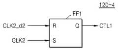
제1논리 회로(120-4)는 제2클럭 신호(CLK2)와 제2B클럭 신호(CLK2_d2)에 기초하여 제1지연회로(120-2) 및 제2지연회로(120-3)에서의 지연 값의 합에 상응하는 펄스폭을 갖는 제1제어신호(CTL1)를 생성시킨다. 예로서, 제2클럭 신호(CLK2)의 펄스가 발생되는 시점부터 제2B클럭 신호(CLK2_d2)의 펄스가 발생되는 시점까지의 구간 폭을 갖는 제1제어신호(CTL1)를 생성시킬 수 있다.The first logic circuit 120-4 delays in the first delay circuit 120-2 and the second delay circuit 120-3 based on the second clock signal CLK2 and the second B clock signal CLK2_d2. The first control signal CTL1 having a pulse width corresponding to the sum of values is generated. For example, a first control signal CTL1 having a section width from a time when the pulse of the second clock signal CLK2 is generated to a time when the pulse of the 2B clock signal CLK2_d2 is generated may be generated.
제2논리 회로(120-5)는 제2디지털 신호(DAC_err)에 포함된 극성 비트 정보에 상응하는 논리 값을 갖는 제2제어신호(CTL2)를 생성시킨다. 예로서, 제2디지털 신호(DAC_err)의 극성 정보를 나타내는 최상위 비트 값에 대응되는 논리 값을 갖는 제2제어신호(CTL2)를 생성시킬 수 있다.The second logic circuit 120-5 generates a second control signal CTL2 having a logic value corresponding to the polarity bit information included in the second digital signal DAC_err. For example, a second control signal CTL2 having a logic value corresponding to a most significant bit value representing polarity information of the second digital signal DAC_err may be generated.
다른 예로서, 아날로그-디지털 변환 처리부(110)에서 생성되는 제2디지털 신호(DAC_err)의 극성 비트 출력을 제2논리 회로(120-5)를 거치지 않고 바로 제2제어신호(CTL2)로 이용할 수도 있다. 세부적으로, 제2디지털 신호(DAC_err)의 극성 정보를 나타내는 최상위 비트 출력을 바로 제2제어신호(CTL2)로 이용할 수도 있다. 이 경우에, 제2논리 회로(120-5)를 생략할 수 있다.As another example, the polarity bit output of the second digital signal (DAC_err) generated by the analog-to-
도 8은 도 7에 도시된 제1지연회로(120-2)의 세부 구성의 일 예를 보여주는 도면이다.8 is a view showing an example of a detailed configuration of the first delay circuit 120-2 shown in FIG.
도 8에 도시된 바와 같이, 제1지연회로(120-2)는 복수의 개의 D플립-플롭들(121-1 ~ 121-v) 및 멀티플렉서(122)를 포함한다.As illustrated in FIG. 8, the first delay circuit 120-2 includes a plurality of D flip-flops 121-1 to 121-v and the
D플립-플롭의 개수 v는 제2디지털 신호(DAC_err)를 구성하는 제1파트의 비트들의 값에 기초하여 결정된다. 예로서, 제1파트의 비트들의 개수가 4개인 경우에 D플립-플롭의 개수 v를 (24-1)인 15개로 결정할 수 있다.The number of D flip-flops v is determined based on the values of the bits of the first part constituting the second digital signal DAC_err. For example, when the number of bits of the first part is 4, the number of D flip-flops v may be determined to be 15 (24 -1).
복수의 개의 D플립-플롭들(121-1 ~ 121-v)은 직렬로 연결된다. 세부적으로 첫 번째 D플립-플롭(121-1)의 입력 단자(D)에는 제2클럭 신호(CLK2)가 인가되고, 출력 단자(Q)를 다음 D플립-플롭(121-2)의 입력 단자(D)에 연결한다. 이와 같은 방식으로 D플립-플롭들(121-1 ~ 121-v)의 입력 단자(D) 및 출력 단자(Q)를 연결시킨다. The plurality of D flip-flops 121-1 to 121-v are connected in series. In detail, the second clock signal CLK2 is applied to the input terminal D of the first D flip-flop 121-1, and the output terminal Q is input to the next D flip-flop 121-2. Connect to (D). In this way, the input terminal D and the output terminal Q of the D flip-flops 121-1 to 121-v are connected.
그리고, 복수의 개의 D플립-플롭들(121-1 ~ 121-v)의 각 클럭 단자(CK)에는 제1클럭 신호(CLK1)가 인가된다.Also, a first clock signal CLK1 is applied to each clock terminal CK of the plurality of D flip-flops 121-1 to 121-v.
그러면, 첫 번째 D플립-플롭(121-1)에서는 제1클럭 신호(CLK1)의 1주기 지연된 제2클럭 신호(CLK2)가 출력되고, 두 번째 D플립-플롭(121-1)에서는 제1클럭 신호(CLK1)의 2주기 지연된 제2클럭 신호(CLK2)가 출력되고, 마지막 D플립-플롭(121-v)에서는 제1클럭 신호(CLK1)의 v주기 지연된 제2클럭 신호(CLK2)가 출력된다.Then, the first D flip-flop 121-1 outputs the second clock signal CLK2 delayed by one cycle of the first clock signal CLK1, and the first D flip-flop 121-1 outputs the first D flip-flop 121-1. The second clock signal CLK2 delayed by two cycles of the clock signal CLK1 is output, and the second clock signal CLK2 delayed by the v period of the first clock signal CLK1 is output from the last D flip-flop 121-v. Is output.
첫 번째 D플립-플롭(121-1)의 입력 신호 Q0과 복수의 개의 D플립-플롭들(121-1 ~ 121-v)에서 출력되는 신호 Q1 ~ Qv들은 멀티플렉서(122)로 입력된다.The input signals Q0 of the first D flip-flop 121-1 and the signals Q1 to Qv output from the plurality of D flip-flops 121-1 to 121-v are input to the
멀티플렉서(122)는 제2디지털 신호(DAC_err)를 구성하는 제1파트의 비트들의 값에 의하여 (v+1)개의 입력 단자들로 입력되는 신호 Q0 ~ Qv들 중에서 하나의 신호를 선택하여 출력한다.The
예로서, 제2디지털 신호(DAC_err)를 구성하는 제1파트의 비트들이 [14:11]이고, [14:11] 비트들의 값이 [0000]인 경우에 멀티플렉서(122)는 Q0를 선택하여 출력한다. 다른 예로서, [14:11] 비트들의 값이 [0101]인 경우에 멀티플렉서(122)는 Q5를 선택하여 출력한다.For example, when the bits of the first part constituting the second digital signal DAC_err are [14:11] and the values of [14:11] bits are [0000], the
도 9는 도 7에 도시된 제2지연회로(120-3)의 세부 구성의 일 예를 보여주는 도면이다.9 is a view showing an example of a detailed configuration of the second delay circuit 120-3 shown in FIG.
도 9에 도시된 바와 같이, 제2지연회로(120-3)는 제1디코더(120-3A) 및 제1딜레이 체인(120-3B)을 포함한다.As shown in FIG. 9, the second delay circuit 120-3 includes a first decoder 120-3A and a first delay chain 120-3B.
제1딜레이 체인(120-3B)은 복수개의 딜레이 셀들(123-1 ~ 123-k)이 직렬로 연결되는 회로 구성을 갖는다. 제1딜레이 체인(120-3B)은 제2A클럭 신호(CLK2_d1)를 입력하여, 제1디코딩 신호들(D1 ~Dk)에 기초하여 딜레이 셀들(123-1 ~ 123-k)에 서 지연된 제2B클럭 신호(CLK2_d2)를 출력한다.The first delay chain 120-3B has a circuit configuration in which a plurality of delay cells 123-1 to 123-k are connected in series. The first delay chain 120-3B inputs the second A clock signal CLK2_d1, and the second B delayed in the delay cells 123-1 to 123-k based on the first decoding signals D1 to Dk. The clock signal CLK2_d2 is output.
딜레이 셀들(123-1 ~ 123-k)의 개수 k는 제2디지털 신호(DAC_err)를 구성하는 제2파트의 비트들의 개수와 같게 결정한다. 예로서, 제2디지털 신호(DAC_err)의 [10:0] 비트들을 제2파트의 비트들로 할당한 경우에 딜레이 셀들(123-1 ~ 123-k)의 개수 k는 11개로 결정할 수 있다. 딜레이 셀들(123-1 ~ 123-k)은 제1디코더(120-3A)에서 생성되는 제1디코딩 신호들(D1 ~Dk)에 의하여 제어된다.The number k of delay cells 123-1 to 123-k is determined to be equal to the number of bits of the second part constituting the second digital signal DAC_err. For example, when [10: 0] bits of the second digital signal DAC_err are allocated as bits of the second part, the number k of delay cells 123-1 to 123-k may be determined as 11 bits. The delay cells 123-1 to 123-k are controlled by the first decoding signals D1 to Dk generated by the first decoder 120-3A.
최하위 비트에 대응되는 딜레이 셀(123-1)에서의 지연 시간을 제1단위 지연 시간(dt1)으로 결정하면, 2번째 상위 비트에 대응되는 딜레이 셀(123-2)에서의 지연 시간은 2*dt1로 결정하고, 3번째 상위 비트에 대응되는 딜레이 셀(123-3)의 지연 시간은 4*dt1로 결정하는 방식으로 상위 비트로 올라갈수록 딜레이 셀의 지연 시간은 2배씩 증가하도록 결정한다.If the delay time in the delay cell 123-1 corresponding to the least significant bit is determined as the first unit delay time dt1, the delay time in the delay cell 123-2 corresponding to the second upper bit is 2 *. It is determined by dt1, and the delay time of the delay cell 123-3 corresponding to the third high-order bit is determined by 4 * dt1, so that the delay time of the delay cell increases by 2 times as it goes up to the high-order bit.
예로서, 최하위 비트에 대응되는 딜레이 셀(123-1)에서의 지연 시간인 제1단위 지연 시간(dt1)을 125ps로 결정한 경우에 2번째 상위 비트에 대응되는 딜레이 셀(123-2)에서의 지연 시간을 0.25ns로 결정할 수 있다. 그리고, 11번째 상위 비트에 대응되는 딜레이 셀(123-11)에서의 지연 시간을 32ns로 결정할 수 있다.For example, when the first unit delay time dt1, which is the delay time in the delay cell 123-1 corresponding to the least significant bit, is determined to be 125 ps, in the delay cell 123-2 corresponding to the second higher bit. The delay time can be determined to be 0.25 ns. In addition, the delay time in the delay cell 123-11 corresponding to the 11th upper bit may be determined to be 32 ns.
제1디코더(120-3A)는 제2디지털 신호(DAC_err)를 구성하는 제2파트의 비트들의 값에 기초하여 딜레이 체인(120-3A)을 구성하는 딜레이 셀들을 선택하기 위한 제1디코딩 신호들(D1 ~Dk)을 생성한다. 제1디코더(120-3A)의 제1디코딩 값을 제2디지털 신호(DAC_err)를 구성하는 제2파트의 비트들의 값과 동일한 값으로 결정할 수 있다. 예로서, 제2디지털 신호(DAC_err)를 구성하는 제2파트의 비트들의 값이 [01000000011]인 경우에, 제1디코딩 값을 [01000000011]로 결정할 수 있다. 그리고, 제1디코딩 값 [01000000011]에 따른 제1디코딩 신호들(D1 ~D11)을 생성할 수 있다. 제1디코딩 신호들(D1~Dk) 각각을 딜레이 셀들을 일대일로 매칭시킨다.The first decoders 120-3A are the first decoding signals for selecting the delay cells constituting the delay chain 120-3A based on the values of the bits of the second part constituting the second digital signal DAC_err. Create (D1 ~ Dk). The first decoding value of the first decoder 120-3A may be determined to be the same value as the bits of the second parts constituting the second digital signal DAC_err. For example, when the values of the bits of the second part constituting the second digital signal DAC_err are [01000000011], the first decoding value may be determined as [01000000011]. Then, the first decoding signals D1 to D11 according to the first decoding value [01000000011] may be generated. Each of the first decoding signals D1 to Dk matches the delay cells one-to-one.
제1딜레이 체인(120-3A)을 구성하는 딜레이 셀들 중에서 제1디코딩 신호들(D0~Dk)의 값에 기초하여 선택된 딜레이 셀(들)은 해당 셀의 지연 시간만큼 입력 신호를 지연시켜 출력한다. 그리고, 딜레이 체인(120-3A)을 구성하는 딜레이 셀들 중에서 선택되지 않은 딜레이 셀(들)은 제2단위 지연 시간(dt2)만큼 입력 신호를 지연시킨다. 여기에서, 제2단위 지연 시간(dt2)은 제1단위 지연 시간(dt1)보다 작은 값으로 설정한다. 제2단위 지연 시간(dt2)은 제1단위 지연 시간(dt1)에 비하여 무시할 수 있을 정도로 작은 값으로 설정하는 것이 바람직하다.The delay cell (s) selected based on the values of the first decoding signals D0 to Dk among the delay cells constituting the first delay chain 120-3A are output by delaying the input signal by the delay time of the corresponding cell. . Then, the delay cell (s) not selected among the delay cells constituting the delay chain 120-3A delays the input signal by the second unit delay time dt2. Here, the second unit delay time dt2 is set to a value smaller than the first unit delay time dt1. It is preferable to set the second unit delay time dt2 to a value small enough to be neglected compared to the first unit delay time dt1.
예로서, 제2디지털 신호(DAC_err)의 [10:0] 비트들의 값이 [01000000011]인 경우에, 디코딩 신호들(D0~Dk)에 의하여 선택되는 딜레이 셀들은 (123-1), (123-2), (123-10)가 된다. 만일 단위 지연 시간을 무시한다면 딜레이 체인(120-3A)에서의 총 지연 시간은 3개의 딜레이 셀들 (123-1), (123-2), (123-10)에 대한 지연 시간들의 합이 된다.For example, when the values of the [10: 0] bits of the second digital signal DAC_err are [01000000011], the delay cells selected by the decoding signals D0 to Dk are (123-1), (123) -2), (123-10). If the unit delay time is ignored, the total delay time in the delay chain 120-3A is the sum of the delay times for the three delay cells 123-1, 123-2, and 123-10.
도 10은 도 9에 도시된 제1딜레이 체인(120-3B)의 세부 구성의 일 예를 보여주는 도면이다.10 is a view showing an example of a detailed configuration of the first delay chain (120-3B) shown in FIG.
도 10에 도시된 바와 같이, 제1딜레이 체인(120-3B)은 복수개의 딜레이 셀들(123-1 ~ 123-k)이 직렬로 연결된다. 복수개의 딜레이 셀들(123-1 ~ 123-k) 각각은 해당 딜레이 셀의 지연 시간에 상응되는 개수의 제1단위 지연 시간(dt1)을 갖는 딜레이 소자(DL_dt1)를 직렬로 연결한 제1단자, 제1단자와 병렬로 연결된 제2단위 지연 시간(dt1)을 갖는 딜레이 소자(DL_dt2)의 제2단자 중에서 스위칭 소자(SWi)에 의하여 하나의 단자를 선택하여 출력한다. 스위칭 소자(SWi)는 제2디지털 신호(DAC_err)를 구성하는 제1파트의 비트들에 기초하여 디코더(120-3A)에 의하여 생성된 제1디코딩 신호(Di)에 의하여 제어된다.10, the first delay chain (120-3B) is a plurality of delay cells (123-1 ~ 123-k) are connected in series. Each of the plurality of delay cells 123-1 to 123-k is a first terminal connected in series with a delay element DL_dt1 having a first unit delay time dt1 corresponding to the delay time of the corresponding delay cell, One terminal is selected and output by the switching element SWi from the second terminal of the delay element DL_dt2 having the second unit delay time dt1 connected in parallel with the first terminal. The switching element SWi is controlled by the first decoding signal Di generated by the decoder 120-3A based on the bits of the first part constituting the second digital signal DAC_err.
세부적으로, 딜레이 셀(123-1)은 입력 신호를 제1단위 지연 시간(dt1)만큼 지연시켜 출력하는 하나의 딜레이 소자(DL_dt1), 딜레이 소자(DL_dt1)와 병렬로 연결되어 제2단위 지연 시간(dt1)만큼 지연시켜 출력하는 하나의 딜레이 소자(DL_dt2) 및 스위칭 소자(SW1)로 구성된다. 스위칭 소자(SW1)에 의하여 딜레이 소자(DL_dt1) 또는 딜레이 소자(DL_dt2) 중의 하나를 선택하여 출력한다. 스위칭 소자(SW1)는 제2디지털 신호(DAC_err)를 구성하는 제1파트의 비트들 중의 최하위 비트에 상응하는 제1디코딩 신호(D1)에 의하여 제어된다. 예로서, 제1디코딩 신호(D1)가 제1논리 값(예로서, 1)을 갖는 경우에, 딜레이 셀(123-1)은 딜레이 소자(DL_dt1)에서 지연된 신호를 선택하여 출력한다. 그리고, 제1디코딩 신호(D1)가 제2논리 값(예로서, 0)을 갖는 경우에, 딜레이 셀(123-1)은 딜레이 소자(DL_dt2)에서 지연된 신호를 선택하여 출력한다.In detail, the delay cell 123-1 is connected in parallel with one delay element DL_dt1 and the delay element DL_dt1 that outputs by delaying the input signal by the first unit delay time dt1, and the second unit delay time. It consists of one delay element (DL_dt2) and a switching element (SW1) for outputting with a delay of (dt1). One of the delay element DL_dt1 or the delay element DL_dt2 is selected and output by the switching element SW1. The switching element SW1 is controlled by the first decoding signal D1 corresponding to the least significant bit of the bits of the first part constituting the second digital signal DAC_err. For example, when the first decoding signal D1 has a first logic value (eg, 1), the delay cell 123-1 selects and outputs a delayed signal from the delay element DL_dt1. Then, when the first decoding signal D1 has a second logic value (eg, 0), the delay cell 123-1 selects and outputs a delayed signal from the delay element DL_dt2.
딜레이 셀(123-k)은 직렬로 연결된 2k개의 딜레이 소자(DL_dt1)들, 하나의 딜레이 소자(DL_dt2) 및 스위칭 소자(SWk)로 구성된다. 스위칭 소자(SWk)는 직렬로 연결된 2k개의 딜레이 소자(DL_dt1)들에 의하여 지연된 신호가 출력되는 제1단자, 제1단자와 병렬로 연결된 하나의 딜레이 소자(DL_dt2)에 의하여 지연된 신호가 출력되는 제2단자 중의 하나를 선택한다. 스위칭 소자(SWk)는 제2디지털 신호(DAC_err)를 구성하는 제1파트의 비트들 중의 최상위 비트에 상응하는 제1디코딩 신호(Dk)에 의하여 제어된다. 예로서, 제1디코딩 신호(Dk)가 제1논리 값(예로서, 1)을 갖는 경우에, 딜레이 셀(123-k)은 2k개의 딜레이 소자(DL_dt1)에서 지연된 신호를 출력하도록 제1단자를 선택한다. 그리고, 제1디코딩 신호(Dk)가 제2논리 값(예로서, 0)을 갖는 경우에, 딜레이 셀(123-k)은 딜레이 소자(DL_dt2)에서 지연된 신호를 출력하도록 제2단자를 선택한다.The delay cell 123-k is composed of 2k delay elements DL_dt1 connected in series, one delay element DL_dt2 and a switching element SWk. The switching element SWk is a first terminal for outputting a delayed signal by 2k delay elements DL_dt1 connected in series, and a delayed signal by a delay element DL_dt2 connected in parallel with the first terminal. Select one of the second terminals. The switching element SWk is controlled by the first decoding signal Dk corresponding to the most significant bit of the bits of the first part constituting the second digital signal DAC_err. For example, when the first decoding signal Dk has a first logic value (eg, 1), the delay cell 123-k is the first to output a delayed signal from 2k delay elements DL_dt1. Select a terminal. Then, when the first decoding signal Dk has a second logic value (eg, 0), the delay cell 123-k selects the second terminal to output the delayed signal from the delay element DL_dt2. .
도 11은 도 7에 도시된 제1논리 회로(120-4)의 세부 구성의 일 예를 보여주는 도면이다.11 is a view showing an example of a detailed configuration of the first logic circuit 120-4 shown in FIG.
도 11에 도시된 바와 같이, 제1논리 회로(120-4)는 제1RS 플립-플롭(FF1)에 의하여 구현될 수 있다.As illustrated in FIG. 11, the first logic circuit 120-4 may be implemented by the first RS flip-flop FF1.
제1RS 플립-플롭(FF1)의 R단자에는 제2지연회로(120-3)에서 출력되는 제2B클럭 신호(CLK2_d2)가 인가되고, S단자에는 제1분주기(120-1)에서 출력되는 제2클럭 신호(CLK2)가 인가된다.The 2B clock signal CLK2_d2 output from the second delay circuit 120-3 is applied to the R terminal of the first RS flip-flop FF1, and the first terminal 120-1 is output to the S terminal. The second clock signal CLK2 is applied.
예로서, 제2클럭 신호(CLK2)가 도 16(B)와 같은 타이밍으로 발생되고 제2B클럭 신호(CLK2_d2)가 도 16(D)와 같은 타이밍으로 발생되면, 제1RS 플립-플롭(FF1)의 출력 단자(Q)에서 출력되는 제1제어신호(CTL1)는 도 16(E)와 같이 발생된다.For example, if the second clock signal CLK2 is generated at the timing shown in FIG. 16 (B) and the second clock signal CLK2_d2 is generated at the same timing as FIG. 16 (D), the first RS flip-flop FF1 The first control signal CTL1 output from the output terminal Q is generated as shown in FIG. 16 (E).
도 12는 도 1에 도시된 위상 합성부(120B)의 세부 구성의 다른 예를 보여주는 도면이다.12 is a view showing another example of the detailed configuration of the
도 12에 도시된 바와 같이, 위상 합성부(120B)는 제1분주기(120-1), 제1지연회로(120-2), 제2지연회로(120-3), 제1논리 회로(120-4), 제2논리 회로(120-5) 및 캘리브레이션 회로(120-6)를 포함한다. 또한, 도 12의 제2지연회로(120-3)는 도 9의 제2지연회로(120-3)과 실질적으로 동일할 수 있다.12, the
위상 합성부(120B)는 도 7에 도시된 위상 합성부(120A)에 캘리브레이션 회로(120-6)가 추가된 구성을 갖는다. 제1분주기(120-1), 제1지연회로(120-2), 제2지연회로(120-3), 제1논리 회로(120-4) 및 제2논리 회로(120-5)에 대해서는 도 7에서 상세히 설명하였으므로, 중복적인 설명은 피하기로 한다.The
캘리브레이션 회로(120-6)는 캘리브레이션 정보 산출부(120-6A) 및 제4곱셈기(120-6B)를 포함한다. The calibration circuit 120-6 includes a calibration information calculator 120-6A and a fourth multiplier 120-6B.
캘리브레이션 정보 산출부(120-6A)는 제2지연회로(120-3)에서의 제1클럭 신호(CLK1)의 1주기 동안에 지연되는 값에 상응하는 스큐 캘리브레이션 값을 산출한다. 여기에서, 스큐 캘리브레이션 값은 제2지연회로(120-3)에 의하여 발생되는 제1클럭 신호(CLK1)의 스큐 값과 동일한 값이 된다.The calibration information calculating unit 120-6A calculates a skew calibration value corresponding to a value delayed during one cycle of the first clock signal CLK1 in the second delay circuit 120-3. Here, the skew calibration value becomes the same value as the skew value of the first clock signal CLK1 generated by the second delay circuit 120-3.
제4곱셈기(120-6B)는 위상 합성부(120B)로 입력되는 제2디지털 신호(DAC_err)를 구성하는 제2파트의 비트들에 스큐 캘리브레이션 값을 곱하여 정규화된 제2파트의 비트들의 값을 출력한다. 제4곱셈기(120-6B)에서 출력되는 정규화된 제2파트의 비트들의 값은 제2지연 회로(120-3)에 인가된다.The fourth multiplier 120-6B multiplies the bits of the second part constituting the second digital signal DAC_err input to the
이에 따라서, 제2지연 회로(120-3)에서 발생되는 공정 특성 및 전압 변동에 따른 지연량 변동을 상쇄시킬 수 있게 된다.Accordingly, it is possible to compensate for the variation in delay amount due to process characteristics and voltage variations generated in the second delay circuit 120-3.
도 13은 도 12에 도시된 캘리브레이션 회로(120-6)의 세부 구성의 일 예를 보여주는 도면이다.13 is a diagram showing an example of a detailed configuration of the calibration circuit 120-6 shown in FIG.
도 13에 도시된 바와 같이, 캘리브레이션 회로(120-6)는 제2'지연 회로(120-3'), 제2분주기(124), RS 플립-플롭(125), 디코더 제어부(126) 및 제4곱셈기(120-6B)를 포함한다.13, the calibration circuit 120-6 includes a second 'delay circuit 120-3', a
제2분주기(124)는 제1클럭 신호(CLK1)를 입력하여, 제1클럭 신호(CLK1)를 2분주하여 출력한다. 예로서, 제1클럭 신호(CLK1)의 주파수가 32MHz인 경우에 분주기(124)에서는 16MHz의 클럭 신호가 출력된다. 제2분주기(124)에서 출력되는 신호를 제1A클럭 신호(CLK1A)라고 표시하고 한다.The
제2'지연 회로(120-3')는 도 9에 도시된 제2지연 회로(120-3)와 동동한 회로로 구성된다. 제2'지연 회로(120-3')는 제2디코더(120-3A') 및 제2딜레이 체인(130-3B')를 포함한다. 제2딜레이 체인(120-3B')은 복수개의 딜레이 셀들(123-1' ~ 123-k')이 직렬로 연결된다.The second 'delay circuit 120-3' is composed of the same circuit as the second delay circuit 120-3 shown in FIG. The second 'delay circuit 120-3' includes a second decoder 120-3A 'and a second delay chain 130-3B'. In the second delay chain 120-3B ', a plurality of delay cells 123-1' to 123-k 'are connected in series.
제2딜레이 체인(130-3B')에는 제1A클럭 신호(CLK1A)가 입력된다. 제2딜레이 체인(130-3B')는 제2디코더(120-3A')에서 출력되는 제2디코딩 신호들(D1'~ Dk')에 의하여 딜레이 셀들(123-1' ~ 123-k')을 제어함으로써 제1A클럭 신호(CLK1A)를 지연시킨다. 제2딜레이 체인(130-3B')에서 출력되는 신호를 제1B클럭 신호(CLK1A_d)라고 정의하자.The first A clock signal CLK1A is input to the second delay chain 130-3B '. The second delay chain 130-3B 'is delay cells 123-1' to 123-k 'by the second decoding signals D1' to Dk 'output from the second decoder 120-3A'. The 1A clock signal CLK1A is delayed by controlling. Let's define a signal output from the second delay chain 130-3B 'as a first B clock signal CLK1A_d.
RS 플립-플롭(125)의 R단자에는 제1B클럭 신호(CLK1A_d)가 인가되고, S단자에는 제1A클럭 신호(CLK1A)가 인가된다. RS 플립-플롭(125)의 출력단자(Q)에서 출력되는 신호는 디코더 제어부(126)에 인가된다.A 1B clock signal CLK1A_d is applied to the R terminal of the RS flip-
디코더 제어부(126)는 RS 플립-플롭(125)의 Q단자로 출력되는 신호의 논리 값에 기초하여 제2디코더(120-3A')의 디폴트 값으로 설정된 제2디코딩 값을 증가시키거나 감소시키는 동작을 통하여 스큐 캘리브레이션 값을 생성시킨다. Q단자로 출력되는 신호의 논리 값에 기초하여 k비트로 구성된 제2디코딩 값을 1씩 증가시키거나 감소시킬 수 있다.The
제2디코더(120-3A')는 디코더 제어부(126)에 의하여 제어된 제2디코딩 값에 대응되는 제2디코딩 신호들(D1'~ Dk')을 제2딜레이 체인(130-3B')으로 출력한다.The second decoder 120-3A 'converts the second decoding signals D1' to Dk 'corresponding to the second decoding value controlled by the
세부적으로, 제2딜레이 체인(130-3B')에서의 초기 스큐 값에 따라서 RS 플립-플롭(125)의 Q단자로는 제2논리 값(예로서, 0)이 출력된다. 제2논리 값(예로서, 0)이 디코더 제어부(123)로 인가되면, 디코더 제어부(123)는 제2디코딩 값을 증가시킨다. RS 플립-플롭(125)으로부터 디코더 제어부(126)로 제1논리 값(예로서, 1)이 인가될 때까지 제2디코딩 값은 증가하게 된다. 그리고, RS 플립-플롭(125)으로부터 디코더 제어부(126)로 제1논리 값(예로서, 1)이 인가되면 제2디코딩 값을 감소시킨다.In detail, the second logic value (eg, 0) is output to the Q terminal of the RS flip-
이에 따라서, 제2'지연회로(120-3')에서의제1클럭 신호(CLK1)의 1주기 동안에 지연되는 값에 상응하는 제2디코더(120-3A')의 제2디코딩 값에서 업/다운을 반복하면서 수렴하게 된다. 이와 같이 수렴된 제2디코딩 값이 스큐 캘리브레이션 값이 된다.Accordingly, in the second 'delay circuit (120-3') Convergence while repeating up / down at the second decoding value of the second decoder 120-3A 'corresponding to the delayed value during one period of the first clock signal CLK1. The converged second decoding value becomes a skew calibration value.
제4곱셈기(120-6B)는 위상 합성부(120B)로 입력되는 제2디지털 신호(DAC_err)를 구성하는 제2파트의 비트들에 디코더 제어부(123)에서 생성된 스큐 캘리브레이션 값을 곱하여 정규화된 제2파트의 비트들의 값을 출력한다. 제4곱셈기(120-6B)에서 출력되는 정규화된 제2파트의 비트들의 값은 제2지연 회로(120-3)에 인가된다.The fourth multiplier 120-6B is normalized by multiplying the bits of the second part constituting the second digital signal (DAC_err) input to the
도 14는 도 1a 또는 도 1b에 도시된 챠지 펌프 회로(130)의 세부 구성의 일 예를 보여주는 도면이다.14 is a view showing an example of a detailed configuration of the
도 14에 도시된 바와 같이, 챠지 펌프 회로(130)는 전처리부(130A) 및 챠지 펌프(130B)를 포함한다.As shown in FIG. 14, the
본 발명의 일실시 예에서는 전처리부(130A)가 챠지 펌프 회로(130)에 포함되도록 설계하였으나, 챠지 펌프 회로(130)로부터 분리되도록 설계할 수도 있다. 다른 예로서, 전처리부(130A)를 위상 합성부(120)에 포함되도록 설계할 수도 있다.In one embodiment of the present invention, the
전처리부(130A)는 위상 합성부(120)로부터 입력되는 제1제어신호(CTL1) 및 제2제어신호(CTL2)를 이용하여 챠지 펌프의 충전 또는 방전 동작을 스위칭하는 충전 제어신호(CTL_ch) 및 방전 제어신호(CTL_dis)를 생성시킨다.The
예로서, 전처리부(130A)는 인버터(131)와 2개의 제1,2AND 게이트(132, 133)로 구성된다.For example, the
제2제어신호(CTL2)는 인버터(131)의 입력 단자 및 제2AND 게이트(133)의 제2입력 단자에 인가된다. 제1제어신호(CTL1)는 제1AND 게이트(132)의 제2입력 단자 및 제2AND 게이트(133)의 제1입력 단자에 인가된다. 그리고, 인버터(131)의 출력 신호는 제1AND 게이트(132)의 제1입력 단자에 인가된다.The second control signal CTL2 is applied to the input terminal of the
이에 따라서, 제1AND 게이트(132)는 제2제어신호(CTL2)의 논리 상태가 '0'이고 제1제어신호(CTL1)의 논리 상태가 '1'인 경우에 논리 상태 '1'인 제1충전 제어신호(CTL_ch)를 출력하고, 그 외의 경우에는 논리 상태 '0'인 제1충전 제어신호(CTL_ch)를 출력한다.Accordingly, the first AND
예로서, 제2제어신호(CTL2)가 도 16(F)와 같은 타이밍으로 발생되고 제1제어신호(CTL1)가 도 16(E)와 같은 타이밍으로 발생되면, 제1충전 제어신호(CTL_ch)는 도 16(H)와 같은 타이밍으로 발생된다.For example, when the second control signal CTL2 is generated at the timing shown in FIG. 16 (F) and the first control signal CTL1 is generated at the same timing as FIG. 16 (E), the first charge control signal CTL_ch Is generated at the same timing as in Fig. 16 (H).
그리고, 제2AND 게이트(133)는 제2제어신호(CTL2)의 논리 상태가 '1'이고 제1제어신호(CTL1)의 논리 상태가 '1'인 경우에 논리 상태 '1'인 제1방전 제어신호(CTL_dis)를 출력하고, 그 외의 경우에는 논리 상태 '0'인 제1방전 제어신호(CTL_dis)를 출력한다. In addition, the second AND
예로서, 제2제어신호(CTL2)가 도 16(F)와 같은 타이밍으로 발생되고 제1제어신호(CTL1)가 도 16(E)와 같은 타이밍으로 발생되면, 제1방전 제어신호(CTL_dis)는 도 16(G)와 같은 타이밍으로 발생된다.For example, if the second control signal CTL2 is generated at the timing shown in FIG. 16 (F) and the first control signal CTL1 is generated at the same timing as FIG. 16 (E), the first discharge control signal CTL_dis Is generated at the same timing as in Fig. 16 (G).
챠지 펌프(130B)는 스위치(SW), 소스 전류원(Io), 싱크 전류원(Id), 커패시터들(C1, C2) 및 저항 Ro로 구성된다. Vc는 디지털-아날로그 변환 장치(100A 또는 100B)에 인가되는 전원 전압을 나타낸다.The
챠지 펌프(130B)에서 충전 루프가 선택될 때 소스 전류원(Io)은 턴 온(turn on) 되고 싱크 전류원(Id)은 턴 오프(turn off)된다. 그리고, 챠지 펌프(130B)에서 방전 루프가 선택될 때 싱크 전류원(Id)은 턴 온(turn on) 되고 소스 전류원(Io)은 턴 오프(turn off)된다.When the charge loop is selected in the
전처리부(130A)로부터 논리 상태 '1'인 제1충전 제어신호(CTL_ch)가 스위치(SW)에 인가되면, 스위치(SW)는 챠지 펌프(130B)에서 충전 루프를 형성시킨다. 충전 루프가 형성되면 소스 전류원(Io)은 턴 온(turn on) 되고 싱크 전류원(Id)은 턴 오프(turn off)된다. 이에 따라서, 소스 전류원(Io)에서 출력되는 전류는 커패시터 C1 및 C2로 공급된다. 커패시터 C1 및 C2가 충전됨에 따라서 챠지 펌프(130B)의 출력 전압(Vo)은 증가한다. 챠지 펌프(130B)의 출력 전압(Vo)은 충전 루프가 형성되는 구간의 길이에 비례하여 증가한다. 그리고, 충전 루프가 형성되는 구간의 길이는 제1제어신호(CTL1)의 논리 상태가 '1'을 유지하는 구간의 길이에 따라 결정된다.When the first charge control signal CTL_ch in the logic state '1' is applied from the
전처리부(130A)로부터 논리 상태 '1'인 제1방전 제어신호(CTL_dis)가 스위치(SW)에 인가되면, 스위치(SW)는 챠지 펌프(130B)에서 방전 루프를 형성시킨다. 방전 루프가 형성되면 싱크 전류원(Id)은 턴 온(turn on) 되고 소스 전류원(Io)은 턴 오프(turn off)된다. 이에 따라서, 커패시터 C1 및 C2에 충전된 전압이 접지 단자를 통하여 방전된다. 즉, 싱크 전류원(Id)을 통하여 방전 전류가 접지 단자로 흐르게 된다. 이에 따라서 커패시터 C1 및 C2에 충전된 전압이 방전됨에 따라서 챠지 펌프(130B)의 출력 전압(Vo)은 감소한다. 챠지 펌프(130B)의 출력 전압(Vo)은 방전 루프가 형성되는 구간의 길이에 비례하여 증가한다. 그리고, 방전 루프가 형성되는 구간의 길이는 제1제어신호(CTL1)의 논리 상태가 '1'을 유지하는 구간의 길이에 따라 결정된다.When the first discharge control signal CTL_dis in the logic state '1' is applied from the
충전 제어신호(CTL_ch) 및 방전 제어신호(CTL_dis)가 모두 논리 상태 '0'을 유지하는 구간에서 챠지 펌프(130B)의 충전 루프 및 방전 루프가 모두 개방된다. 충전 루프 및 방전 루프가 모두 개방된 구간에서 누설 전류를 무시하면 챠지 펌프(130B)의 출력 전압(Vo)은 변동되지 않는다. 도 1a와 같은 디지털-아날로그 변환 장치(100A)의 출력 단자의 전압은 챠지 펌프 회로(130)의 출력 전압(Vo)이 된다.In a section in which the charge control signal CTL_ch and the discharge control signal CTL_dis both maintain the logic state '0', both the charge loop and the discharge loop of the
도 17은 본 발명의 실시 예들에 따른 디지털-아날로그 변환 장치가 적용된 전자 장치(1000)의 구현 예를 보여주는 도면이다.17 is a diagram illustrating an implementation example of an
도 17에 도시된 바와 같이, 전자 장치(1000)는 중앙 처리 장치(CPU; 1100), 신호 처리부(1200), 사용자 인터페이스(1300), 저장부(1400), 장치 인터페이스(1500) 및 버스(1600)를 포함한다.As shown in FIG. 17, the
전자 장치(1000)는 예로서 컴퓨터, 모바일 폰, PDA, PMP, MP3 플레이어, 카메라, 캠코더, TV 수상기, 디스플레이 기기 등이 포함될 수 있다.The
중앙 처리 장치(1100)는 전자 장치(1000)를 전반적으로 제어하는 동작을 수행한다. 예로서, 사용자 인터페이스(1300)를 통하여 입력되는 정보에 기초하여 전자 장치(1000)의 구성 수단들을 제어할 수 있다.The
신호 처리부(1200)는 장치 인터페이스(1500)를 통하여 수신되는 신호 또는 저장부(1400)로부터 읽어낸 신호를 정해진 규격에 맞추어 처리한다. 예로서, 비디오 신호 처리 또는 오디오 신호 처리 등을 수행할 수 있다. 신호 처리부(1200)에는 본 발명의 실시 예에 따른 디지털-아날로그 변환 장치(DAC; 100A 또는 100B)가 포함된다. 예로서, 디지털-아날로그 변환 장치(100A 또는 100B)는 전자 장치(1000)에서의 비디오 신호 처리, 오디오 신호 처리 또는 전원 전압 신호 처리 등에 적용될 수 있다.The
사용자 인터페이스(1300)는 전자 장치(1000)의 기능 설정 및 동작에 필요한 정보를 사용자가 설정하기 위한 입력 장치이다.The
저장부(1400)는 전자 장치(1000)의 동작에 필요한 각종 정보들이 저장된다. 또한, 장치 인터페이스(1500)를 통하여 수신되는 데이터 또는 전자 장치(1000)에서 처리된 데이터들이 저장될 수 있다.The
장치 인터페이스(1500)는 전자 장치(1000)와 유선 또는 무선으로 접속되는 외부 장치와의 데이터 통신을 수행한다.The
버스(1600)는 전자 장치(1000)의 구성 수단들 간의 정보를 전송하는 기능을 수행한다.The
그러면, 도 17의 전자 장치(1000)에서 수행되는 본 발명의 실시 예에 따른 디지털-아날로그 변환 방법에 대하여 설명하기로 한다.Then, a digital-analog conversion method according to an embodiment of the present invention performed in the
도 18은 본 발명의 다른 실시 예에 따른 디지털-아날로그 변환 방법의 흐름도이다.18 is a flowchart of a digital-to-analog conversion method according to another embodiment of the present invention.
전자 장치(1000)는 출력 단자의 아날로그 전압 신호를 제1디지털 신호로 변환하는 신호 처리를 수행한다(S110). 예로서, 출력 단자는 디지털-아날로그 변환 장치의 출력 단자가 될 수 있다.The
전자 장치(1000)는 제1디지털 신호와 타깃 디지털 신호(DAC_tar)의 차에 상응하는 제2디지털 신호(DAC_err)를 생성시키는 동작을 수행한다(S120). 여기에서, 제2디지털 신호(DAC_err)는 디지털 에러 신호를 의미한다. 예로서, 제2디지털 신호(DAC_err)는 극성 정보를 나타내는 비트와 에러 정보를 나타내는 비트들로 구성될 수 있다. 세부적으로, 제2디지털 신호(DAC_err)의 최상위 비트로 극성 정보를 나타내고, 최상위 비트를 제외한 나머지 비트들로 에러 정보를 나타낼 수 있다.The
다음으로, 전자 장치(1000)는 제2디지털 신호(DAC_err)에 기초한 클럭 주기 단위의 지연 제어 및 클럭 주기 내에서의 스큐 제어에 따라서 생성된 신호들의 위상 합성을 통하여 챠지 펌프 제어신호를 생성하는 동작을 수행한다(S130). 예로서, 챠지 펌프 제어신호는 제2디지털 신호(DAC_err)에 포함된 극성 정보에 상응하는 논리 상태를 갖는 제2제어신호(CTL2) 및 제2디지털 신호(DAC_err)에 포함된 에러 정보에 상응하는 펄스폭을 갖는 제1제어신호(CTL1)가 포함될 수 있다.Next, the
다음으로, 전자 장치(1000)는 챠지 펌프 제어신호에 기초한 챠지 펌프 회로에서의 충전 또는 방전 시간의 조절에 의하여 아날로그 전압 신호를 생성시키는 동작을 수행한다(S140). 제2제어신호(CTL2)의 논리 상태에 기초하여 챠지 펌프 회로의 충전 루프 또는 방전 루프를 선택하고, 선택된 루프에서 제1제어신호(CTL1)의 펄스폭에 상응하는 구간 동안에 전류를 흘린다. 이와 같은 제어를 통하여 챠지 펌프 회로에서 아날로그 신호가 출력된다.Next, the
도 19는 도 18에 도시된 아날로그 신호를 생성시키는 단계(S130)에 대한 세부 흐름도를 예시적으로 보여주는 도면이다.19 is a diagram showing a detailed flow chart for the step of generating the analog signal shown in FIG. 18 (S130).
전자 장치(1000)는 제2디지털 신호(DAC_err)에 포함된 극성 비트 정보에 기초하여 챠지 펌프 회로의 충전 루프 또는 방전 루프를 선택하는 제2제어신호(CTL2)를 생성시키는 동작을 수행한다(S130-1). 예로서, 제2디지털 신호(DAC_err)의 극성 정보를 나타내는 최상위 비트의 출력으로서 제2제어신호(CTL2)를 생성시킬 수 있다.The
전자 장치(1000)는 제2디지털 신호(DAC_err)를 이용한 위상 합성 처리를 통하여 제1제어신호(CTL1)를 생성시키는 동작을 수행한다(S130-2). 예로서, 제2디지털 신호(DAC_err)를 구성하는 제1파트의 비트들의 값에 기초한 클럭 주기 단위의 지연 제어 및 제2디지털 신호(DAC_err)를 구성하는 제2파트의 비트들의 값에 기초한 클럭 주기 내에서의 스큐 제어에 따라서 생성된 신호들의 위상 합성을 통하여 제1제어신호(CTL1)를 생성시킬 수 있다. 세부적으로, 제2디지털 신호(DAC_err)에 포함된 에러 정보에 상응하는 펄스폭을 갖는 제1제어신호(CTL1)를 생성시킨다.The
도 20은 도 19에 도시된 제1제어신호(CTL1)를 생성시키는 단계(S130-2)에 대한 세부 흐름도를 예시적으로 보여주는 도면이다.FIG. 20 exemplarily shows a detailed flowchart of step S130-2 of generating the first control signal CTL1 shown in FIG.
전자 장치(1000)는 제2디지털 신호(DAC_err)를 구성하는 제1파트의 비트들의 값에 기초하여 제2클럭 신호(CLK2)를 지연시킨 제2A클럭 신호(CLK2_d1)를 생성시킨다(S130-2A). 예로서, 제2디지털 신호(DAC_err)를 구성하는 제1파트의 비트들의 값에 기초하여 제2클럭 신호(CLK2)를 제1클럭 신호(CLK1)의 1주기 시간 단위로 지연시킨 제2A클럭 신호(CLK2_d1)를 생성시킨다. 제2클럭 신호(CLK2)는 제1클럭 신호(CLK1)의 2 이상의 초기 설정된 정수배 주기마다 펄스를 발생하는 신호이다.The
전자 장치(1000)는 제2디지털 신호(DAC_err)를 구성하는 제2파트의 비트들의 값에 기초한 스큐 제어에 따라서 제2A클럭 신호(CLK2_d1)를 지연시킨 제2B클럭 신호(CLK2_d2)를 생성시킨다(S130-2B). 예로서, 제2디지털 신호(DAC_err)를 구성하는 제2파트의 비트들의 값에 기초하여 스큐 제어에 따라서 제2A클럭 신호(CLK2_d1)를 초기 설정된 분해능 시간 단위로 지연시킨 제2B클럭 신호(CLK2_d2)를 출력할 수 있다. 예로서, 초기 값으로 설정되는 분해능 시간 단위는 제1클럭 신호(CLK1)의 1주기 시간 단위를 2K(K=제2파트의 비트들의 개수)로 분할한 시간 단위로 결정할 수 있다. 다른 예로서, 초기 값으로 설정되는 분해능 시간 단위는 제1클럭 신호의 1주기 시간 단위를2K(K=제2파트의 비트들의 개수)로 분할한 시간 단위보다 일정량 크거나 작게 결정할 수도 있다.The
전자 장치(1000)는 제2클럭 신호(CLK2)와 제2B클럭 신호(CLK2_d2)의 위상을 합성하여 제2디지털 신호에 포함된 에러 정보에 상응하는 펄스폭을 갖는 제1제어신호(CTL1)를 생성시킨다(S130-2C). 예로서, 에러 정보는 제2디지털 신호(DAC_err)를 구성하는 제1파트의 비트들과 제2파트의 비트들에 의하여 표현될 수 있다. 예로서, 제2클럭 신호(CLK2)의 펄스가 발생되는 시점부터 제2B클럭 신호(CLK2_d2)의 펄스가 발생되는 시점까지의 구간 폭을 갖는 제1제어신호(CTL1)를 생성시킬 수 있다.The
이상에서와 같이 도면과 명세서에서 최적 실시예가 개시되었다. 여기서 특정한 용어들이었으나, 이는 단지 본 발명을 설명하기 위한 목적에서 사용된 것이지 의미 한정이나 특허청구범위에 기재된 본 발명의 범위를 제한하기 위하여 사용된 것은 아니다. 그러므로 본 기술 분야의 통상의 지식을 가진 자라면 이로부터 다양한 변형 및 균등한 타 실시예가 가능하다는 점을 이해할 것이다. 따라서, 본 발명의 진정한 기술적 보호범위는 첨부된 특허청구범위의 기술적 사상에 의해 정해져야 할 것이다.As described above, optimal embodiments have been disclosed in the drawings and specifications. Although these are specific terms, they are only used for the purpose of describing the present invention and are not used to limit the scope of the present invention as defined in the claims or the claims. Therefore, those of ordinary skill in the art will understand that various modifications and other equivalent embodiments are possible therefrom. Therefore, the true technical protection scope of the present invention should be determined by the technical spirit of the appended claims.
100A, 100B : 디지털-아날로그 변환 장치
110 : 아날로그-디지털 변환 처리부 120 : 위상 합성부
130 : 챠지 펌프 회로 140 : 아날로그 버퍼 회로
110-1A, 110-1B : 제1,2아날로그-디지털 변환기
110-2A : 감산 회로 110-2B : 디지털 필터
111 : 기준 전압 발생 회로 112 : 비교 회로
113 : 인코더 11, 12, 13, 120-6B : 제1,2,3,4곱셈기
14 : 합산기 16 : 감산기
17 : 베럴 시프터 18 : 후처리기
120-1 : 제1분주기 120-2, 120-3 : 제1,2지연 회로
120-4, 120-5 : 제1,2논리 회로
121-1 ~ 121-v : D플립 플롭 122 : 멀티플렉서
120-3A, 120-3A' : 제1,2디코더
123-1 ~ 123-k, 123-1' ~ 123-k' : 딜레이 셀
120-6 : 캘리브레이션 회로 120-6A : 캘리브레이션 정보 산출부
125 : RS 플립 플롭 126 : 디코더 제어부
1000 : 전자 장치 1100 : 중앙 처리 장치
1200 : 신호 처리부 1400 : 저장부
1500 : 장치 인터페이스 1600 : 버스100A, 100B: Digital-to-analog converter
110: analog-to-digital conversion processing unit 120: phase synthesis unit
130: charge pump circuit 140: analog buffer circuit
110-1A, 110-1B: 1st, 2nd analog-to-digital converter
110-2A: Subtraction circuit 110-2B: Digital filter
111: reference voltage generation circuit 112: comparison circuit
113:
14: Totalizer 16: Subtractor
17: barrel shifter 18: post-processor
120-1: 1st divider 120-2, 120-3: 1st, 2nd delay circuit
120-4, 120-5: 1st, 2nd logic circuit
121-1 ~ 121-v: D flip-flop 122: multiplexer
120-3A, 120-3A ': 1st, 2nd decoder
123-1 ~ 123-k, 123-1 '~ 123-k': Delay Cell
120-6: calibration circuit 120-6A: calibration information calculation unit
125: RS flip-flop 126: decoder control unit
1000: electronic device 1100: central processing unit
1200: signal processing unit 1400: storage unit
1500: Device interface 1600: Bus
Claims (10)
Translated fromKorean상기 제2디지털 신호에 기초한 클럭 주기 단위의 지연 및 클럭 주기 내에서의 스큐 지연에 따라서 생성되는 신호들의 위상 합성 처리에 의하여 상기 제2디지털 신호에 포함된 에러 정보에 상응하는 펄스폭을 갖는 제1제어신호를 생성시키는 위상 합성부; 및
상기 제2디지털 신호에 포함된 극성 정보에 기초하여 충전 루프 또는 방전 루프를 선택하고, 상기 선택된 루프에서 상기 제1제어신호의 펄스폭에 상응하는 구간 동안에 흐르는 전류에 따라서 아날로그 전압 신호를 생성시키는 챠지 펌프 회로를 포함함을 특징으로 하는 디지털-아날로그 변환 장치.An analog-to-digital conversion processor configured to convert an analog voltage signal at an output terminal into a first digital signal and generate a second digital signal corresponding to a difference between the first digital signal and a target digital signal;
A first having a pulse width corresponding to error information included in the second digital signal by phase synthesis processing of signals generated according to a delay in a clock period unit and a skew delay in a clock period based on the second digital signal. A phase synthesis unit generating a control signal; And
A charge that selects a charge loop or a discharge loop based on polarity information included in the second digital signal, and generates an analog voltage signal according to a current flowing during a section corresponding to the pulse width of the first control signal in the selected loop. Digital to analog conversion device comprising a pump circuit.
상기 출력 단자의 아날로그 전압 신호를 N(N은 2이상의 정수)비트의 제1A디지털 신호로 변환하는 제1아날로그-디지털 변환기; 및
상기 N비트의 제1A디지털 신호와 N비트의 타깃 디지털 신호의 차에 상응하는 N비트의 제2디지털 신호를 생성시키는 감산 회로를 포함함을 특징으로 하는 디지털-아날로그 변환 장치.According to claim 1, The analog-to-digital conversion processing unit
A first analog-to-digital converter for converting the analog voltage signal of the output terminal into a 1A digital signal of N (N is an integer of 2 or more) bits; And
And a subtraction circuit generating an N-bit second digital signal corresponding to a difference between the N-bit 1A digital signal and the N-bit target digital signal.
상기 출력 단자의 아날로그 전압 신호를 M(M은 2이상의 정수)비트의 제1B디지털 신호로 변환하는 제2아날로그-디지털 변환기; 및
상기 제1B디지털 신호를 입력하여 평균 필터링 처리 및 타깃 디지털 신호와의 감산 처리에 기초하여 N(N은 M보다 큰 정수)비트의 제2디지털 신호를 출력하는 디지털 필터를 포함함을 특징으로 하는 디지털-아날로그 변환 장치.According to claim 1, The analog-to-digital conversion processing unit
A second analog-to-digital converter for converting the analog voltage signal of the output terminal into a 1B digital signal of M (M is an integer of 2 or more) bits; And
And a digital filter for inputting the 1B digital signal and outputting a second digital signal of N (N is an integer greater than M) bit based on the average filtering process and the subtraction process with the target digital signal. -Analog conversion device.
제1클럭 신호의 2 이상의 초기 설정된 정수배 주기마다 펄스가 발생되는 제2클럭 신호를 생성하는 제1분주기;
상기 제2디지털 신호를 구성하는 제1파트의 비트들의 값에 기초하여 상기 제2클럭 신호를 상기 제1클럭 신호의 1주기 시간 단위로 지연시킨 제2A클럭 신호를 생성시키는 제1지연회로;
상기 제2디지털 신호를 구성하는 제2파트의 비트들의 값에 기초한 클럭 스큐 제어에 따라서 상기 제2A클럭 신호를 초기 설정된 분해능 시간 단위로 지연시킨 제2B클럭 신호를 생성시키는 제2지연회로; 및
상기 제2클럭 신호와 제2B클럭 신호에 기초하여 상기 제1지연회로 및 상기 제2지연회로에서의 지연 값의 합에 상응하는 펄스폭을 갖는 제1제어신호를 생성시키는 논리 회로를 포함함을 특징으로 하는 디지털-아날로그 변환 장치.The method of claim 1, wherein the phase synthesis unit
A first divider for generating a second clock signal in which a pulse is generated every two or more initially set integer multiples of the first clock signal;
A first delay circuit for generating a 2A clock signal in which the second clock signal is delayed by one cycle time unit of the first clock signal based on the values of the bits of the first part constituting the second digital signal;
A second delay circuit for generating a 2B clock signal in which the 2A clock signal is delayed in units of an initially set resolution time according to clock skew control based on the values of bits of the second part constituting the second digital signal; And
And a logic circuit for generating a first control signal having a pulse width corresponding to a sum of delay values in the first delay circuit and the second delay circuit based on the second clock signal and the second B clock signal. Digital-to-analog conversion device.
상기 제2파트의 비트들의 개수에 상응하는 딜레이 셀들이 직렬로 연결된 제1딜레이 체인; 및
상기 제2파트의 비트들의 값에 기초하여 상기 딜레이 셀들의 동작을 제어하는 제1디코더를 포함하고, 상기 딜레이 체인의 딜레이 셀들의 지연 시간은 최하위 비트에 상응하는 딜레이 셀의 지연 시간을 기준으로 1비트씩 상위 비트로 이동함에 따라 2배씩 증가하도록 설정하는 것을 특징으로 하는 디지털-아날로그 변환 장치.The method of claim 6, wherein the second delay circuit
A first delay chain in which delay cells corresponding to the number of bits of the second part are connected in series; And
And a first decoder that controls the operation of the delay cells based on the value of the bits of the second part, and the delay time of the delay cells in the delay chain is based on the delay time of the delay cell corresponding to the least significant bit. Digital-to-analog conversion device characterized in that it is set to increase by 2 times as it moves from bit to bit.
상기 제1디지털 신호와 타깃 디지털 신호의 차에 상응하는 제2디지털 신호를 생성시키는 단계;
상기 제2디지털 신호에 기초한 클럭 주기 단위의 지연 제어 및 클럭 주기 내에서의 스큐 제어에 따라서 생성되는 신호들의 위상 합성을 통하여 챠지 펌프 제어신호를 생성시키는 단계; 및
상기 챠지 펌프 제어신호에 기초한 챠지 펌프 회로에서의 충전 또는 방전 시간의 조절에 의하여 상기 출력 단자로 아날로그 전압 신호를 생성시키는 단계를 포함함을 특징으로 하는 디지털-아날로그 변환 방법.Converting the analog voltage signal at the output terminal into a first digital signal;
Generating a second digital signal corresponding to a difference between the first digital signal and a target digital signal;
Generating a charge pump control signal through phase synthesis of signals generated according to delay control in a clock period unit based on the second digital signal and skew control in a clock period; And
And generating an analog voltage signal to the output terminal by adjusting the charge or discharge time in the charge pump circuit based on the charge pump control signal.
상기 제2디지털 신호에 포함된 극성 비트 정보에 기초하여 상기 챠지 펌프 회로의 충전 루프 또는 방전 루프를 선택하는 제2제어신호를 생성시키는 단계; 및
상기 제2디지털 신호에 기초한 클럭 주기 단위의 지연 및 클럭 주기 내에서의 스큐 지연에 따라서 생성되는 신호들의 위상 합성 처리에 의하여 상기 제2디지털 신호에 포함된 에러 정보에 상응하는 펄스폭을 갖는 제1제어신호를 생성시키는 단계를 포함함을 특징으로 하는 디지털-아날로그 변환 방법.10. The method of claim 9, The step of generating the charge pump control signal
Generating a second control signal for selecting a charge loop or a discharge loop of the charge pump circuit based on the polarity bit information included in the second digital signal; And
A first having a pulse width corresponding to error information included in the second digital signal by phase synthesis processing of signals generated according to a delay in a clock period unit and a skew delay in a clock period based on the second digital signal. Digital-to-analog conversion method comprising the step of generating a control signal.
Priority Applications (2)
| Application Number | Priority Date | Filing Date | Title |
|---|---|---|---|
| KR1020130153309AKR102094469B1 (en) | 2013-12-10 | 2013-12-10 | Apparatus and method for converting digital signal to analog signal |
| US14/549,736US9065478B1 (en) | 2013-12-10 | 2014-11-21 | Digital to-analog conversion apparatuses and methods |
Applications Claiming Priority (1)
| Application Number | Priority Date | Filing Date | Title |
|---|---|---|---|
| KR1020130153309AKR102094469B1 (en) | 2013-12-10 | 2013-12-10 | Apparatus and method for converting digital signal to analog signal |
Publications (2)
| Publication Number | Publication Date |
|---|---|
| KR20150067622A KR20150067622A (en) | 2015-06-18 |
| KR102094469B1true KR102094469B1 (en) | 2020-03-27 |
Family
ID=53272221
Family Applications (1)
| Application Number | Title | Priority Date | Filing Date |
|---|---|---|---|
| KR1020130153309AActiveKR102094469B1 (en) | 2013-12-10 | 2013-12-10 | Apparatus and method for converting digital signal to analog signal |
Country Status (2)
| Country | Link |
|---|---|
| US (1) | US9065478B1 (en) |
| KR (1) | KR102094469B1 (en) |
Families Citing this family (7)
| Publication number | Priority date | Publication date | Assignee | Title |
|---|---|---|---|---|
| US10122378B2 (en)* | 2017-03-16 | 2018-11-06 | Samsung Electronics Co., Ltd. | Digital-to-time converter and operating method thereof |
| US10944415B2 (en)* | 2018-06-27 | 2021-03-09 | Massachusetts Institute Of Technology | Spectrally efficient digital logic (SEDL) analog to digital converter (ADC) |
| US10673417B2 (en) | 2018-06-27 | 2020-06-02 | Massachusetts Institute Of Technology | Spectrally efficient digital logic |
| JP7374627B2 (en)* | 2019-06-28 | 2023-11-07 | キヤノン株式会社 | Digital-to-analog conversion circuits, display devices, electronic equipment |
| US10868562B1 (en)* | 2020-02-10 | 2020-12-15 | Taiwan Semiconductor Manufacturing Company Limited | Loop gain auto calibration using loop gain detector |
| US12418298B2 (en)* | 2023-02-10 | 2025-09-16 | Apple Inc. | Localized IQ mismatch measurement and compensation systems and methods |
| CN117131915A (en)* | 2023-09-15 | 2023-11-28 | 李承逸 | Method, equipment and medium for artificial intelligent computation |
Citations (2)
| Publication number | Priority date | Publication date | Assignee | Title |
|---|---|---|---|---|
| US20120200328A1 (en) | 2011-02-04 | 2012-08-09 | Chih-Wei Yao | Reference Clock Compensation for Fractional-N Phase Lock Loops (PLLs) |
| US20140354335A1 (en) | 2013-05-28 | 2014-12-04 | Broadcom Corporation | Digital Phase Locked Loop with Hybrid Delta-Sigma Phase/Frequency Detector |
Family Cites Families (20)
| Publication number | Priority date | Publication date | Assignee | Title |
|---|---|---|---|---|
| GB9014679D0 (en) | 1990-07-02 | 1990-08-22 | Sarnoff David Res Center | Sequential successive approximation a/d converter |
| US5604465A (en) | 1995-06-07 | 1997-02-18 | International Business Machines Corporation | Adaptive self-calibration for fast tuning phaselock loops |
| US6275685B1 (en) | 1998-12-10 | 2001-08-14 | Nortel Networks Limited | Linear amplifier arrangement |
| US6160449A (en) | 1999-07-22 | 2000-12-12 | Motorola, Inc. | Power amplifying circuit with load adjust for control of adjacent and alternate channel power |
| US6329850B1 (en)* | 1999-12-27 | 2001-12-11 | Texas Instruments Incorporated | Precision frequency and phase synthesis |
| KR20010095928A (en) | 2000-04-12 | 2001-11-07 | 오종훈 | Non-linearity and error correction method for switching power amplification of a pulse width modulated signal with a/d converter |
| TW536678B (en) | 2000-11-28 | 2003-06-11 | Winbond Electronics Corp | Device and method for automatically generating test programs of test mechanism |
| US6874097B1 (en) | 2001-06-01 | 2005-03-29 | Maxtor Corporation | Timing skew compensation technique for parallel data channels |
| US6885227B2 (en) | 2003-07-29 | 2005-04-26 | Lattice Semiconductor Corporation | Clock generator with skew control |
| US7443326B2 (en) | 2003-10-27 | 2008-10-28 | Dan Raphaeli | Digital input signals constructor providing analog representation thereof |
| US7148749B2 (en) | 2005-01-31 | 2006-12-12 | Freescale Semiconductor, Inc. | Closed loop power control with high dynamic range |
| US7706160B2 (en) | 2006-08-08 | 2010-04-27 | Marco Fontana | High voltage generator of the DAC-controlled type |
| KR20080067466A (en) | 2007-01-16 | 2008-07-21 | 삼성전자주식회사 | Delay sync loop |
| KR100904425B1 (en) | 2007-10-12 | 2009-06-26 | 주식회사 하이닉스반도체 | Skew compensation circuit |
| US7940202B1 (en) | 2008-07-31 | 2011-05-10 | Cypress Semiconductor Corporation | Clocking analog components operating in a digital system |
| US8134486B2 (en) | 2009-08-17 | 2012-03-13 | Taiwan Semiconductor Manufacturing Company, Ltd. | DAC calibration |
| CN102025327B (en) | 2009-09-18 | 2013-01-02 | 富士通株式会社 | Amplifier apparatus and predistortion control method |
| US8380138B2 (en) | 2009-10-21 | 2013-02-19 | Qualcomm Incorporated | Duty cycle correction circuitry |
| US8248282B2 (en) | 2010-08-17 | 2012-08-21 | Texas Instruments Incorporated | Track and hold architecture with tunable bandwidth |
| US8907681B2 (en) | 2011-03-11 | 2014-12-09 | Taiwan Semiconductor Manufacturing Company, Ltd. | Timing skew characterization apparatus and method |
- 2013
- 2013-12-10KRKR1020130153309Apatent/KR102094469B1/enactiveActive
- 2014
- 2014-11-21USUS14/549,736patent/US9065478B1/enactiveActive
Patent Citations (2)
| Publication number | Priority date | Publication date | Assignee | Title |
|---|---|---|---|---|
| US20120200328A1 (en) | 2011-02-04 | 2012-08-09 | Chih-Wei Yao | Reference Clock Compensation for Fractional-N Phase Lock Loops (PLLs) |
| US20140354335A1 (en) | 2013-05-28 | 2014-12-04 | Broadcom Corporation | Digital Phase Locked Loop with Hybrid Delta-Sigma Phase/Frequency Detector |
Also Published As
| Publication number | Publication date |
|---|---|
| KR20150067622A (en) | 2015-06-18 |
| US9065478B1 (en) | 2015-06-23 |
| US20150162934A1 (en) | 2015-06-11 |
Similar Documents
| Publication | Publication Date | Title |
|---|---|---|
| KR102094469B1 (en) | Apparatus and method for converting digital signal to analog signal | |
| JP6703265B2 (en) | Neural network device and method for controlling neural network device | |
| CN101677237B (en) | Clock timing calibration circuit, clock timing calibration method and analog-to-digital conversion system | |
| KR102188059B1 (en) | LDO regulator, power management system and LDO voltage control method | |
| US9584145B1 (en) | Circuit for and method of compensating for mismatch in a time-interleaved analog-to-digital converter | |
| US8842029B2 (en) | Area-efficiency delta modulator for quantizing an analog signal | |
| JP2018050282A (en) | Successive approximation resister ad converter | |
| WO2019043359A1 (en) | Modulators | |
| CN110086470A (en) | The control method of analog-digital converter and analog-digital converter | |
| CN106357271A (en) | Excess loop delay compensation circuit, excess loop compensation method and continuous time delta-sigma analog-digital converter | |
| JP2014075684A (en) | Ad conversion circuit, semiconductor device and ad conversion method | |
| US9509327B2 (en) | A/D converter and A/D converter calibrating method | |
| US6980139B2 (en) | Sigma-delta-modulator | |
| JP5695629B2 (en) | Successive comparison type A / D converter and multi-bit delta-sigma modulator using the same | |
| US9525431B1 (en) | Feed forward sigma-delta ADC modulator | |
| CN116248119B (en) | Digital-to-analog conversion circuit, chip and electronic equipment for PWM conversion analog output | |
| JP2010226454A (en) | Gain control circuit and electronic volume circuit having the same | |
| CN111817553B (en) | On-chip charge pump circuit | |
| US8653997B2 (en) | Modulator | |
| Mori et al. | High-resolution DPWM generator for digitally controlled DC-DC converters | |
| KR20150025262A (en) | Digital Controlled Oscillator and Electronic Device including Digital Controlled Oscillator | |
| CN112514262A (en) | Processing circuit | |
| WO2025091091A1 (en) | System and method for single cycle dynamic hysteresis error control | |
| JP4856659B2 (en) | Semiconductor integrated circuit device | |
| JP5451317B2 (en) | Continuous-time multi-bit ΔΣ ADC circuit |
Legal Events
| Date | Code | Title | Description |
|---|---|---|---|
| PA0109 | Patent application | Patent event code:PA01091R01D Comment text:Patent Application Patent event date:20131210 | |
| PG1501 | Laying open of application | ||
| A201 | Request for examination | ||
| PA0201 | Request for examination | Patent event code:PA02012R01D Patent event date:20181113 Comment text:Request for Examination of Application Patent event code:PA02011R01I Patent event date:20131210 Comment text:Patent Application | |
| E902 | Notification of reason for refusal | ||
| PE0902 | Notice of grounds for rejection | Comment text:Notification of reason for refusal Patent event date:20190826 Patent event code:PE09021S01D | |
| E701 | Decision to grant or registration of patent right | ||
| PE0701 | Decision of registration | Patent event code:PE07011S01D Comment text:Decision to Grant Registration Patent event date:20200221 | |
| GRNT | Written decision to grant | ||
| PR0701 | Registration of establishment | Comment text:Registration of Establishment Patent event date:20200323 Patent event code:PR07011E01D | |
| PR1002 | Payment of registration fee | Payment date:20200324 End annual number:3 Start annual number:1 | |
| PG1601 | Publication of registration | ||
| PR1001 | Payment of annual fee | Payment date:20230222 Start annual number:4 End annual number:4 | |
| PR1001 | Payment of annual fee | Payment date:20240227 Start annual number:5 End annual number:5 | |
| PR1001 | Payment of annual fee | Payment date:20250225 Start annual number:6 End annual number:6 |