KR102088883B1 - Organic Light Emitting Display Device - Google Patents
Organic Light Emitting Display DeviceDownload PDFInfo
- Publication number
- KR102088883B1 KR102088883B1KR1020130148536AKR20130148536AKR102088883B1KR 102088883 B1KR102088883 B1KR 102088883B1KR 1020130148536 AKR1020130148536 AKR 1020130148536AKR 20130148536 AKR20130148536 AKR 20130148536AKR 102088883 B1KR102088883 B1KR 102088883B1
- Authority
- KR
- South Korea
- Prior art keywords
- region
- host
- dopant
- light emitting
- mlct1
- Prior art date
- Legal status (The legal status is an assumption and is not a legal conclusion. Google has not performed a legal analysis and makes no representation as to the accuracy of the status listed.)
- Active
Links
Images


Classifications
- H—ELECTRICITY
- H10—SEMICONDUCTOR DEVICES; ELECTRIC SOLID-STATE DEVICES NOT OTHERWISE PROVIDED FOR
- H10K—ORGANIC ELECTRIC SOLID-STATE DEVICES
- H10K50/00—Organic light-emitting devices
- H10K50/10—OLEDs or polymer light-emitting diodes [PLED]
- H10K50/11—OLEDs or polymer light-emitting diodes [PLED] characterised by the electroluminescent [EL] layers
- H10K50/12—OLEDs or polymer light-emitting diodes [PLED] characterised by the electroluminescent [EL] layers comprising dopants
- H10K50/121—OLEDs or polymer light-emitting diodes [PLED] characterised by the electroluminescent [EL] layers comprising dopants for assisting energy transfer, e.g. sensitization
- H—ELECTRICITY
- H10—SEMICONDUCTOR DEVICES; ELECTRIC SOLID-STATE DEVICES NOT OTHERWISE PROVIDED FOR
- H10K—ORGANIC ELECTRIC SOLID-STATE DEVICES
- H10K50/00—Organic light-emitting devices
- H10K50/10—OLEDs or polymer light-emitting diodes [PLED]
- H10K50/11—OLEDs or polymer light-emitting diodes [PLED] characterised by the electroluminescent [EL] layers
- H10K50/12—OLEDs or polymer light-emitting diodes [PLED] characterised by the electroluminescent [EL] layers comprising dopants
Landscapes
- Physics & Mathematics (AREA)
- Optics & Photonics (AREA)
- Electroluminescent Light Sources (AREA)
- Devices For Indicating Variable Information By Combining Individual Elements (AREA)
Abstract
Translated fromKoreanDescription
Translated fromKorean본 발명은 유기전계발광표시장치에 관한 것이다.The present invention relates to an organic light emitting display device.
유기전계발광표시장치에 사용되는 유기전계발광소자는 기판 상에 위치하는 두 개의 전극 사이에 발광층이 형성된 자발광소자이다.An organic light emitting device used in an organic light emitting display device is a self-emitting device in which a light emitting layer is formed between two electrodes positioned on a substrate.
유기전계발광표시장치는 빛이 방출되는 방향에 따라 전면발광(Top-Emission) 방식, 배면발광(Bottom-Emission) 방식 또는 양면발광(Dual-Emission) 방식 등이 있다.The organic light emitting display device includes a top-emission method, a bottom-emission method, or a dual-emission method according to the direction in which light is emitted.
유기전계발광표시장치에는 적색, 녹색 및 청색을 발광하는 유기발광소자를 이용하여 영상을 구현하는 방식과 백색을 발광하는 유기발광소자와 적색, 녹색 및 청색 등의 컬러필터를 이용하여 영상을 구현하는 방식이 있다.In the organic light emitting display device, an image is implemented using an organic light emitting device emitting red, green, and blue, and an image is implemented using an organic light emitting device emitting white and color filters such as red, green, and blue. There is a way.
유기전계발광표시장치의 발광 재료는 호스트(Host)-도판트(dopant) 시스템을 사용하여 성능을 극대화할 수 있는데, 호스트에서 도판트로의 원활한 에너지 전이가 중요한 요인이 된다.The light emitting material of the organic light emitting display device can maximize performance by using a host-dopant system, and smooth energy transfer from the host to the dopant is an important factor.
형광 재료에서는 쌍극자 쌍극자 상호작용에 의한 에너지 전이가 주로 일어나고 인광 재료에서는 전자 상호 교환에 의한 에너지 전이가 주로 일어난다. 그런데, 인광 재료에서 쌍극자 쌍극자 상호작용에 의한 에너지 전이가 일어날 경우 복잡한 에너지 레벨 때문에 에너지 전이가 원활하지 않아 발광(EL) 스펙트럼의 변화로 인한 시야각 저하 및 효율 저하 등의 문제가 발생하게 되므로 이의 개선이 요구된다.In the fluorescent material, the energy transfer by dipole dipole interaction mainly occurs, and in the phosphorescent material, the energy transfer by electron exchange mainly occurs. However, when the energy transfer due to the dipole dipole interaction occurs in the phosphorescent material, the energy transfer is not smooth due to the complex energy level, which causes problems such as deterioration in viewing angle and efficiency due to changes in the luminescence (EL) spectrum. Is required.
상술한 배경기술의 문제점을 해결하기 위한 본 발명은 형광 재료의 호스트와 인광 재료의 도판트 사용시 호스트의 PL 스펙트럼의 영역을 최적화하여 시야각 특성 및 효율을 향상시킬 수 있는 유기전계발광표시장치를 제공하는 것이다.The present invention for solving the above-mentioned problems of the background art provides an organic light emitting display device capable of improving viewing angle characteristics and efficiency by optimizing the PL spectrum region of the host when using a host of a fluorescent material and a dopant of a phosphorescent material will be.
상술한 과제 해결 수단으로 본 발명은 기판 상에 위치하는 두 개의 전극 사이에 형성된 발광층을 포함하고, 발광층은 형광 재료의 호스트와 인광 재료의 도판트를 포함하며, 형광 재료의 호스트에 의한 호스트 PL 영역은 인광 재료의 도판트에 의한 도판트 UV 흡수 영역 중 하나와 중첩하는 스펙트럼을 나타내는 것을 특징으로 하는 유기전계발광표시장치를 제공한다.As the above-mentioned problem solving means, the present invention includes a light emitting layer formed between two electrodes positioned on a substrate, the light emitting layer includes a host of a fluorescent material and a dopant of a phosphorescent material, and a host PL region by the host of the fluorescent material It provides an organic light emitting display device characterized in that it exhibits a spectrum overlapping one of the dopant UV absorption regions by the dopant of the phosphorescent material.
호스트 PL 영역 내에는 도판트 UV 흡수 영역의 MLCT1 영역이 존재하고, 도판트 UV 흡수 영역의 MLCT3 영역은 일부만 존재할 수 있다.In the host PL region, the MLCT1 region of the dopant UV absorption region is present, and the MLCT3 region of the dopant UV absorption region may be partially present.
호스트 PL 영역은 도판트 UV 흡수 영역의 MLCT1 영역의 피크와 중첩하고, 도판트 UV 흡수 영역의 MLCT3 영역의 피크와 미중첩할 수 있다.The host PL region may overlap the peak of the MLCT1 region of the dopant UV absorption region, and may not overlap the peak of the MLCT3 region of the dopant UV absorption region.
호스트 PL 영역의 반치폭은 도판트 UV 흡수 영역의 MLCT1 영역의 반치폭보다 좁을 수 있다.The half width of the host PL region may be narrower than that of the MLCT1 region of the dopant UV absorption region.
호스트 PL 영역은 도판트 PL 영역과 일부 영역만 중첩할 수 있다.The host PL region may overlap only the dopant PL region and some regions.
발광층은 호스트 영역과, 호스트 및 도판트가 혼합된 혼합 영역과, 도판트 영역을 포함할 수 있다.The emission layer may include a host region, a mixed region in which a host and a dopant are mixed, and a dopant region.
본 발명은 형광 재료의 호스트와 인광 재료의 도판트를 혼합하여 사용하고, 호스트 PL 영역을 인광 도판트 UV 흡수 영역 중 하나와 중첩하도록 제한하는 방식으로 호스트의 스펙트럼 영역을 최적화하여 시야각 특성 및 효율을 향상시킬 수 있는 효과가 있다.The present invention uses a mixture of a host of a fluorescent material and a dopant of a phosphorescent material, and optimizes the spectral region of the host by limiting the host PL region to overlap with one of the phosphorescent dopant UV absorbing regions to improve viewing angle characteristics and efficiency. There is an effect that can be improved.
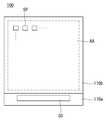
도 1은 유기전계발광표시장치의 개략적인 평면도.
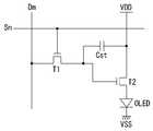
도 2는 도 1에 도시된 서브 픽셀 회로 구성 예시도.
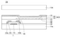
도 3은 도 1에 도시된 서브 픽셀의 단면 예시도.
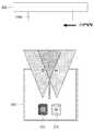
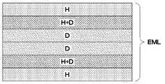
도 4는 발광층의 형성 방법을 설명하기 위한 도면.
도 5는 도 4의 방법에 의해 형성된 발광층의 단면 계층도.
도 6은 종래 인광 도판트로 구현된 표시패널의 파장별 선명도에 대한 측정치를 나타낸 그래프.
도 7은 호스트와 도판트 간의 쌍극자 상호작용에 의한 에너지 전이를 보여주는 도면.
도 8은 본 발명의 실시예에 따른 인광 도판트로 구현된 표시패널의 파장별 선명도에 대한 측정치를 나타낸 그래프.
도 9는 종래 표시패널과 본 발명의 실시예에 따른 표시패널의 비교를 위한 EL 스펙트럼을 나타낸 그래프.
도 10은 종래 표시패널과 본 발명의 실시예에 따른 표시패널의 비교를 위한 시야각 그래프.
도 11은 호스트 재료의 특성별 시야각 차이를 보여주는 그래프.1 is a schematic plan view of an organic light emitting display device.
FIG. 2 is a diagram illustrating the configuration of a sub-pixel circuit shown in FIG. 1.
3 is a cross-sectional example of the sub-pixel shown in FIG. 1.
4 is a view for explaining a method of forming a light emitting layer.
5 is a cross-sectional hierarchical view of a light emitting layer formed by the method of FIG. 4.
6 is a graph showing measurement values of sharpness for each wavelength of a display panel implemented with a conventional phosphorescent dopant.
7 is a diagram showing energy transfer by dipole interaction between a host and a dopant.
8 is a graph showing measurement values of sharpness for each wavelength of a display panel implemented as a phosphorescent dopant according to an exemplary embodiment of the present invention.
9 is a graph showing an EL spectrum for comparison between a conventional display panel and a display panel according to an embodiment of the present invention.
10 is a viewing angle graph for comparison between a conventional display panel and a display panel according to an embodiment of the present invention.
11 is a graph showing differences in viewing angles according to characteristics of a host material.
이하, 본 발명의 실시를 위한 구체적인 내용을 첨부된 도면을 참조하여 설명한다.Hereinafter, with reference to the accompanying drawings, specific content for the practice of the present invention will be described.
도 1은 유기전계발광표시장치의 개략적인 평면도이고, 도 2는 도 1에 도시된 서브 픽셀 회로 구성 예시도이며, 도 3은 도 1에 도시된 서브 픽셀의 단면 예시도이다.FIG. 1 is a schematic plan view of an organic light emitting display device, FIG. 2 is an exemplary diagram of a sub-pixel circuit configuration shown in FIG. 1, and FIG. 3 is an exemplary cross-sectional view of the sub-pixel illustrated in FIG. 1.
도 1에 도시된 바와 같이, 유기전계발광표시장치를 구성하는 표시패널(100)에는 제1기판(110a) 상에 형성된 복수의 서브 픽셀(SP)로 이루어진 표시부(AA)가 포함된다. 제1기판(110a) 상에 형성된 표시부(AA)는 제2기판(110b)에 의해 밀봉된다.As illustrated in FIG. 1, the
제1기판(110a) 상에는 표시부(AA)에 포함된 복수의 서브 픽셀(SP)을 구동하는 구동부(30)가 형성된다. 구동부(30)에는 복수의 서브 픽셀(SP)에 데이터신호를 공급하는 데이터구동부와 스캔신호를 공급하는 스캔구동부가 포함될 수 있다. 그러나 스캔구동부의 경우, 데이터구동부와 구분되어 표시부(AA)의 외곽에 게이트인패널 형태로 형성될 수도 있다.A
도 2에 도시된 바와 같이, 서브 픽셀(SP)은 스캔라인(Sn)으로부터 공급된 스캔 신호에 의하여 데이터라인(Dm)을 통해 공급되는 데이터신호를 전달하는 스위칭 박막 트랜지스터(T1), 데이터 신호를 저장하는 커패시터(Cst), 커패시터(Cst)에 저장된 데이터신호와 제1전원전압(VDD)의 차이에 해당하는 구동전류를 생성하는 구동 박막 트랜지스터(T2) 및 구동전류에 대응되는 빛을 발광하는 유기발광다이오드(OLED)를 포함할 수 있다.As shown in FIG. 2, the sub-pixel SP is a switching thin film transistor T1 that transmits a data signal supplied through the data line Dm by a scan signal supplied from the scan line Sn, and a data signal. The storage capacitor Cst, the driving thin film transistor T2 generating a driving current corresponding to the difference between the data signal stored in the capacitor Cst and the first power voltage VDD, and an organic light emitting light corresponding to the driving current It may include a light emitting diode (OLED).
스위칭 박막 트랜지스터(T1), 커패시터(Cst) 및 구동 박막 트랜지스터(T2) 등은 트랜지스터부로 정의될 수 있다. 위의 설명에서는 트랜지스터부가 2개의 박막 트랜지스터와 1개의 커패시터로 구성된 2T(Transistor)1C(Capacitor)를 예로 설명하였다. 그러나 트랜지스터부는 문턱전압 등을 보상하기 위한 목적으로 N개(N은 2이상 정수)의 박막 트랜지스터와 M개(M은 2 이상 정수)의 커패시터를 포함하도록 구성될 수도 있다. 여기서, 'VSS'는 그라운드 이하의 전압을 전달하는 제2전원전압이다.The switching thin film transistor T1, the capacitor Cst, and the driving thin film transistor T2 may be defined as a transistor unit. In the above description, the transistor unit 2T (Transistor) 1C (Capacitor) composed of two thin film transistors and one capacitor was described as an example. However, the transistor unit may be configured to include N (N is an integer of 2 or more) thin film transistors and M (M is an integer of 2 or more) capacitors for the purpose of compensating for a threshold voltage or the like. Here, 'VSS' is a second power voltage that delivers a voltage below ground.
서브 픽셀(SP)은 적색, 녹색 및 청색을 발광하는 유기발광다이오드를 이용하여 영상을 구현하는 방식과 백색을 발광하는 유기발광다이오드와 적색, 녹색 및 청색 등의 컬러필터를 이용하여 영상을 구현하는 방식이 있다. 그러나, 이하에서는 적색, 녹색 및 청색을 발광하는 유기발광다이오드를 이용하여 영상을 구현하는 방식으로 형성된 서브 픽셀에 대해 설명한다.The sub pixel SP implements an image using an organic light emitting diode that emits red, green, and blue, and an image using an organic light emitting diode that emits white light and color filters such as red, green, and blue. There is a way. However, hereinafter, sub-pixels formed by implementing an image using organic light emitting diodes emitting red, green, and blue will be described.
도 3에 도시된 바와 같이, 서브 픽셀에 포함된 트랜지스터부(T)와 유기발광다이오드(OLED)는 제1기판(110a) 상에 박막 형태로 증착된다.As shown in FIG. 3, the transistor part T and the organic light emitting diode OLED included in the sub-pixel are deposited in the form of a thin film on the
제1기판(110a) 상에는 게이트전극(115)이 형성된다. 게이트전극(115)은 몰리브덴(Mo), 알루미늄(Al), 크롬(Cr), 금(Au), 티타늄(Ti), 니켈(Ni) 및 구리(Cu)로 이루어진 군에서 선택된 하나 또는 이들의 합금일 수 있으며, 단일층 또는 다중층으로 이루어질 수 있다.The
게이트전극(115) 상에는 게이트전극(115)을 절연시키는 제1절연막(120)이 형성된다. 제1절연막(120)은 실리콘 산화막(SiOx), 실리콘 질화막(SiNx) 또는 이들의 이중층으로 이루어질 수 있다.A first
게이트전극(115)과 대응되는 제1절연막(120) 상에는 반도체층(125)이 형성된다. 반도체층(125)은 아몰포스 실리콘(a-Si), 폴리실리콘(poly-Si), 산화물(oxide), 유기물(organic) 등으로 이루어질 수 있다.The
반도체층(125) 상에는 반도체층(125)과 전기적으로 연결되는 소오스전극(130a) 및 드레인전극(130b)이 형성된 소오스전극(130a) 및 드레인전극(130b)은 몰리브덴(Mo), 알루미늄(Al), 크롬(Cr), 금(Au), 티타늄(Ti), 니켈(Ni) 및 구리(Cu)로 이루어진 군에서 선택된 하나 또는 이들의 합금일 수 있으며, 단일층 또는 다중층으로 이루어질 수 있다. 한편, 반도체층(125)과 소오스전극(130a) 및 드레인전극(130b) 사이에는 이들 간의 접촉 저항을 줄이는 오믹콘택층이 형성될 수도 있다.The
게이트전극(115), 반도체층(125), 소오스전극(130a) 및 드레인전극(130b)을 포함하는 박막 트랜지스터(T) 상에는 제2절연막(140)이 형성된다. 제2절연막(140)은 하부 구조의 단차를 완화시키는 평탄화막 또는 보호막일 수 있다. 제2절연막(140)은 폴리이미드(polyimide), 벤조사이클로부틴계 수지(benzocyclobutene series resin), 아크릴레이트(acrylate) 등의 유기물로 이루어질 수 있다. 제2절연막(140)에는 소오스전극(130a) 또는 드레인전극(130b)의 일부를 노출시키는 비어홀(145)이 포함된다.The second
제2절연막(140) 상에는 소오스전극(130a) 또는 드레인전극(130b)과 전기적으로 연결된 하부전극(150)이 형성된다. 하부전극(150)은 ITO(Indium Tin Oxide), IZO(Indium Zinc Oxide), ITZO(Indium Tin Zinc Oxide), ZnO(Zinc Oxide), IGZO(Indium Gallium Zinc Oxide) 및 그라핀(graphene)과 같은 투명도전막으로 이루어질 수 있다. 하부전극(150)은 애노드전극으로 선택된다.A
하부전극(150) 상에는 하부전극(150)을 노출시키는 개구부(156)를 포함하는 뱅크층(155)이 형성된다. 뱅크층(155)은 하부 구조의 단차를 완화시키며 발광영역을 정의하는 화소정의막일 수 있다. 뱅크층(155)은 폴리이미드(polyimide), 벤조사이클로부틴계 수지(benzocyclobutene series resin), 아크릴레이트(acrylate) 등으로 이루어질 수 있다.A
하부전극(150) 상에는 유기발광층(160)이 형성된다. 유기발광층(160)은 적색, 녹색 및 청색을 발광하는 유기물로 이루어질 수 있다. 유기발광층(160)에는 발광층(EML)과 이의 특성 개선을 위한 정공주입층(HIL), 정공수송층(HTL), 전자수송층(ETL) 및 전자주입층(EIL) 이상 4개의 공통층이 포함된다. 공통층의 경우 반드시 4개의 층이 모두 사용되지 않고 이들 중 적어도 하나의 층이 생략되거나 다른 기능층이 더 포함되기도 한다.The
유기발광층(160)을 포함하는 제1기판(110a) 상에는 상부전극(170)이 형성된다. 상부전극(170)은 일함수가 낮은 금속들로 알루미늄(Al), 은(Ag), 마그네슘(Mg), 칼슘(Ca) 또는 이들의 합금 등으로 이루어질 수 있다. 상부전극(170)은 캐소드전극으로 선택된다.The
한편, 위의 설명에서는 표시패널(100)에 형성된 서브 픽셀이 제1기판(110a) 방향으로 빛을 발광하는 배면발광(Bottom-Emission) 방식을 일례로 도시 및 설명하였다. 그러나, 본 발명은 이에 한정되지 않고 전면발광(Top-Emission) 방식이나 양면발광(Dual-Emission) 방식으로 형성될 수도 있다.Meanwhile, in the above description, a bottom-emission method in which a sub-pixel formed in the
도 4는 발광층의 형성 방법을 설명하기 위한 도면이고, 도 5는 도 4의 방법에 의해 형성된 발광층의 단면 계층도이다.4 is a view for explaining a method of forming a light emitting layer, and FIG. 5 is a cross-sectional hierarchical diagram of a light emitting layer formed by the method of FIG. 4.
도 4에 도시된 바와 같이, 유기발광다이오드의 발광층은 호스트(Host)와 도판트(Dopant)를 동시에 증착하는 방식으로 형성한다. 증착 장치의 저면에는 유기소스부(210)가 배치된다.As shown in FIG. 4, the light emitting layer of the organic light emitting diode is formed by depositing a host and a dopant at the same time. The
유기소스부(210) 내에는 도판트 재료(D)를 포함하는 제1소스부(213)와 호스트 재료(H)를 포함하는 제2소스부(215)가 배치된다. 유기소스부(210) 내에 배치된 제1소스부(213)와 제2소스부(215)는 물리적으로 분리되어 있는 상태이지만, 유기소스부(210)를 통과하여 타겟 방향으로 날아갈 때 소스들(D, H)은 일정 영역 중첩된 영역을 갖게 된다.The
스테이지(STG)는 제1기판(110a)을 홀딩한 상태에서 유기소스부(210)의 상부를 스캔하듯이 이동하며 지나간다. 제1기판(110a) 상에는 트랜지스터부와 유기발광다이오드의 하부전극이 형성된 상태이다.The stage STG is moved while passing the upper portion of the
스테이지(STG)는 우측 방향에서 좌측 방향으로 스캔하듯이 이동할 수 있으나 이에 한정되지 않는다. 스테이지(STG)는 일 방향으로 스캔하듯이 이동(예컨대, 우측 방향에서 좌측 방향으로 이동)하거나 양 방향으로 스캔하듯이 이동(예컨대, 우측 방향에서 좌측 방향으로 이동한 후 좌측 방향에서 우측 방향으로 이동)할 수 있다.The stage STG may move as if scanning from the right direction to the left direction, but is not limited thereto. The stage STG moves as if scanning in one direction (for example, moving from right to left) or moves as if scanning in both directions (for example, moves from right to left and then moves from left to right) )can do.
스테이지(STG)의 스캔 횟수에 따라 유기발광다이오드의 발광층을 구성하는 호스트와 도판트의 계층은 다양한 형태로 나타나게 된다.Depending on the number of scans of the stage STG, the layers of the host and the dopant constituting the light emitting layer of the organic light emitting diode appear in various forms.
도 5에 도시된 바와 같이, 유기발광다이오드의 발광층(EML)은 하부부터 상부까지 호스트 영역(H), 호스트 및 도판트가 혼합된 혼합 영역(H+D), 도판트 영역(D), 도판트 영역(D), 호스트 및 도판트 영역가 혼합된 혼합 영역(H+D) 및 호스트 영역(H) 순으로 증착된 계층을 가질 수 있다.As illustrated in FIG. 5, the light emitting layer EML of the organic light emitting diode includes a host region H, a mixed region H + D in which a host and a dopant are mixed, a dopant region D, and a dopant from bottom to top. The base layer D may have a layer deposited in the order of the mixed region H + D and the host region H in which the host and dopant regions are mixed.
도 5에 도시된 유기발광다이오드의 발광층(EML)의 계층 구조는 스테이지가 우측 방향에서 좌측 방향으로 이동하며 1회 스캔을 하였을 때 나타난다. 통상 호스트 재료와 도판트 재료를 동시에 증착하면 도판트 영역(D), 호스트 영역(H) 및 혼합 영역(H+D)으로 나누어진다. 즉, 혼합 영역(H+D)을 제외한 도판트 영역(D) 및 호스트 영역(H)과 같은 싱글 영역이 존재하게 된다.The hierarchical structure of the light emitting layer (EML) of the organic light emitting diode shown in FIG. 5 appears when the stage is moved from right to left and scanned once. In general, when the host material and the dopant material are simultaneously deposited, they are divided into a dopant region (D), a host region (H), and a mixed region (H + D). That is, a single region such as the dopant region D and the host region H except for the mixed region H + D exists.
도판트 영역(D) 및 호스트 영역(H)과 같은 싱글 영역이 존재할 경우, 인광 재료 사용시 호스트와 도판트 간의 거리가 멀어지고 쌍극자 쌍극자 상호 작용에 의한 에너지 전이가 주도적으로 일어나게 된다. 이와 관련된 문제 및 이의 해결 방안에 대해서는 이하에서 다룬다.When a single region such as the dopant region D and the host region H exists, the distance between the host and the dopant increases when the phosphorescent material is used, and energy transfer due to dipole dipole interaction occurs. The related issues and their solutions are discussed below.
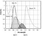
도 6은 종래 인광 도판트로 구현된 표시패널의 파장별 선명도에 대한 측정치를 나타낸 그래프이고, 도 7은 호스트와 도판트 간의 쌍극자 상호작용에 의한 에너지 전이를 보여주는 도면이다. 도 6에서 가로축은 주파수의 파장(Wave length)을 의미하고 세로축은 선명도 또는 광도(Intensity)를 의미한다.FIG. 6 is a graph showing measurements of sharpness for each wavelength of a display panel implemented with a conventional phosphorescent dopant, and FIG. 7 is a diagram showing energy transfer due to dipole interaction between a host and a dopant. In FIG. 6, the horizontal axis represents the wavelength of the frequency (Wave length), and the vertical axis represents the sharpness or intensity.
도 6 및 도 7에 도시된 바와 같이, 종래 인광 도판트로 구현된 표시패널은 호스트 PL(Photoluminescence) 영역(Host PL) 내에, 도판트 UV 흡수 영역(Dopant UV)에서의 MLCT 영역(MLCT1, MLCT3)이 존재한다. MLCT(metal to ligand charge transfer) 영역은 호스트(Host)의 채워진 금속궤도에서 도판트(Dopant)의 빈 리간드 궤도로 전하가 이동하는 쌍극자 에너지 전이가 일어날 수 있는 영역을 의미한다. MLCT1 영역은 싱글렛(S1)에 대한 영역이고, MLCT3 영역은 트리플렛(T1)에 대한 영역이다.6 and 7, the display panel implemented with the conventional phosphorescent dopant is in the host PL (Photoluminescence) region (Host PL), and the MLCT regions (MLCT1, MLCT3) in the dopant UV absorption region (Dopant UV) This exists. The MLCT (metal to ligand charge transfer) region refers to a region in which a dipole energy transfer in which charge moves from a filled metal orbit of a host to an empty ligand orbit of a dopant can occur. The MLCT1 region is for singlet S1, and the MLCT3 region is for triplet T1.
쌍극자 에너지 전이는 자외선 영역(UV) 및 PL 스펙트라(PL spectra.)에서 호스트 PL 영역(Host PL)과 도판트 UV 흡수 영역(Dopant UV)이 중첩될 때 일어난다. 형광 재료에서는 이러한 중첩이 MLCT1 영역과 MLCT3 영역 중 한 영역에서만 일어나므로, 쌍극자 에너지 전이가 MLCT1 영역과 MLCT3 영역 중 한 영역에서만 일어난다. 반면, 인광 재료에서는 이러한 중첩이 MLCT1 영역과 MLCT3 영역 모두에서 일어나므로, 쌍극자 에너지 전이가 MLCT1 영역과 MLCT3 영역 모두에서 일어난다. 즉 이론적으로는, 호스트 PL 영역(Host PL)이 도판트 UV 흡수 영역(Dopant UV)에서의 MLCT1 영역과 중첩될 때, MLCT3 영역과 중첩될 때 또는 MLCT1 영역과 MLCT3 영역에 중첩될 때 모두 에너지 전이가 일어날 수 있다.The dipole energy transfer occurs when the host PL region and the dopant UV absorbing region (Dopant UV) overlap in the ultraviolet region (UV) and PL spectra. In the fluorescent material, the overlap occurs only in one of the MLCT1 region and the MLCT3 region, so dipole energy transfer occurs only in one of the MLCT1 region and the MLCT3 region. On the other hand, in the phosphorescent material, this overlap occurs in both the MLCT1 region and the MLCT3 region, so dipole energy transfer occurs in both the MLCT1 region and the MLCT3 region. That is, in theory, when the host PL region (Host PL) overlaps the MLCT1 region in the dopant UV absorbing region (Dopant UV), the MLCT3 region overlaps, or the MLCT1 region and the MLCT3 region both overlap the energy transfer. Can happen.
하지만, 실험을 통해 알아낸 결과 MLCT3 영역의 에너지 전이는 MLCT1 영역 대비 잘 일어나지 않고 MLCT1 영역과 MLCT3 영역 간에도 에너지 전이가 잘 일어나지 않는다. 즉, 호스트 PL 영역(Host PL)이 도판트 UV 흡수 영역(Dopant UV)의 MLCT1 영역과 MLCT3 영역 간에 또는 MLCT3 영역과 중첩될 경우 에너지 전이가 잘 일어나지 않는다. 때문에, 효율이 떨어지거나 에너지 전이가 되지 않은 영역에서 호스트 PL이 발광하면 발광(이하 EL로 약기함) 스펙트럼이 변화하게 되고 이는 표시패널의 시야각 특성의 저하를 가져온다.However, as a result of finding through experiments, the energy transfer of the MLCT3 region does not occur well compared to the MLCT1 region, and the energy transfer does not occur well between the MLCT1 region and the MLCT3 region. That is, when the host PL region (Host PL) overlaps or overlaps the MLCT1 region and the MLCT3 region of the dopant UV absorbing region (Dopant UV), energy transfer does not easily occur. Therefore, when the host PL emits light in a region where the efficiency is low or the energy is not transferred, the emission (hereinafter abbreviated as EL) spectrum changes, which leads to a decrease in viewing angle characteristics of the display panel.
이를 개선하기 위해, 본 발명은 위의 실험 결과를 기반으로 호스트 PL 영역(Host PL)이 인광 도판트 UV 흡수영역(Dopant UV)에서의 MLCT1 영역하고만 중첩되도록 하여 소자의 특성을 향상하였는데, 이에 대해 설명하면 다음과 같다.To improve this, the present invention improves the characteristics of the device by allowing the host PL region to overlap only with the MLCT1 region in the phosphorescent dopant UV absorption region based on the above experimental results. The explanation is as follows.
도 8은 본 발명의 실시예에 따른 인광 도판트로 구현된 표시패널의 파장별 선명도에 대한 측정치를 나타낸 그래프이고, 도 9는 종래 표시패널과 본 발명의 실시예에 따른 표시패널의 비교를 위한 EL 스펙트럼을 나타낸 그래프이며, 도 10은 종래 표시패널과 본 발명의 실시예에 따른 표시패널의 비교를 위한 시야각 그래프이고, 도 11은 호스트 재료의 특성별 시야각 차이를 보여주는 그래프이다. 도 8 및 도 9에서 가로축은 주파수의 파장(Wave length)을 의미하고 세로축은 선명도 또는 광도(Intensity)를 의미한다.8 is a graph showing measured values of sharpness for each wavelength of a display panel implemented with a phosphorescent dopant according to an embodiment of the present invention, and FIG. 9 is an EL for comparison between a conventional display panel and a display panel according to an embodiment of the present invention It is a graph showing a spectrum, FIG. 10 is a viewing angle graph for comparison between a conventional display panel and a display panel according to an embodiment of the present invention, and FIG. 11 is a graph showing a difference in viewing angle for each property of the host material. 8 and 9, the horizontal axis represents the wavelength of the frequency (Wave length), and the vertical axis represents the clarity or intensity (Intensity).
도 8에 도시된 바와 같이, 본 발명의 실시예에 따르면 호스트 PL 영역(Host PL) 내에는 MLCT1 영역이 존재하고 MLCT3 영역은 존재하지 않도록 형성된다. 즉, 호스트 PL 영역(Host PL)은 MLCT1 영역과 중첩하지만 MLCT3 영역과 중첩하지 않는다.As illustrated in FIG. 8, according to an embodiment of the present invention, the MLCT1 region is present in the host PL region (Host PL) and the MLCT3 region is not present. That is, the host PL region (Host PL) overlaps the MLCT1 region, but does not overlap the MLCT3 region.
그러나, 실질적으로 MLCT1 영역과 MLCT3 영역은 어느 정도 중첩하는 영역을 가지므로 호스트 PL 영역(Host PL) 내에는 MLCT3 영역의 일부만 존재한다. 때문에 더욱 구체적으로 설명하면, 호스트 PL 영역(Host PL)은 MLCT1 영역의 피크와 중첩하지만 MLCT3 영역의 피크와 미중첩하도록 형성된다.However, since the MLCT1 region and the MLCT3 region have overlapping regions to some extent, only a portion of the MLCT3 region exists in the host PL region (Host PL). Therefore, more specifically, the host PL region (Host PL) overlaps the peak of the MLCT1 region, but is formed so as not to overlap the peak of the MLCT3 region.
또한, 호스트 PL 영역(Host PL)의 반치폭은 MLCT1 영역의 반치폭보다 좁다. 또한, 호스트 PL 영역(Host PL)은 도판트 PL 영역(Dopant PL)과 거의 중첩하지 않을 만큼 미소 크기의 중첩 영역(극히 일부 영역만 중첩함)을 갖는다.In addition, the half width of the host PL region (Host PL) is narrower than that of the MLCT1 region. In addition, the host PL region (Host PL) has an overlapping region (only a small portion of the region) having a small size such that it rarely overlaps with the Dopant PL region.
본 발명의 실시예에서는 호스트 재료 등을 포함하는 발광층의 구조를 변경하고 호스트 PL 영역(Host PL)이 차지하는 파장대를 좁히는 방식으로 호스트 PL 영역(Host PL) 내에 MLCT1 영역만 존재하도록 한다. 한편, 실험에 사용된 호스트는 형광 재료이고, 도판트는 인광 재료이다. 그리고 인광 재료인 도판트의 PL 파장대는 380nm ~ 780nm 이다.In the exemplary embodiment of the present invention, only the MLCT1 region is present in the host PL region in a manner of changing the structure of the light emitting layer including the host material and the like and narrowing the wavelength band occupied by the host PL region. Meanwhile, the host used in the experiment is a fluorescent material, and the dopant is a phosphorescent material. In addition, the PL wavelength range of the phosphorescent material dopant is 380 nm to 780 nm.
도 6에 도시된 바와 같이, 종래 표시패널에서 사용된 호스트A재료(Host A)는 호스트 PL 영역(Host PL)이 도판트의 MLCT1 영역과 MLCT3 영역에 모두 중첩된다. 이 때문에, 호스트A재료(Host A)는 우측의 그래프와 같이 호스트 영역에 EL 피크(Peak)가 생성된다.As shown in FIG. 6, in the host A material (Host A) used in the conventional display panel, the host PL region (Host PL) overlaps both the MLCT1 region and the MLCT3 region of the dopant. For this reason, the host A material (Host A) generates an EL peak in the host region as shown in the graph on the right.
반면, 도 9에 도시된 바와 같이, 본 발명의 실시예에 따른 표시패널에서 사용된 호스트B재료(Host B)는 호스트 PL 영역(Host PL)이 도판트의 MLCT1 영역에만 중첩된다. 이 때문에, 호스트B재료(Host B)는 우측의 그래프와 같이 호스트 영역에 EL 피크가 생성되지 않는다.On the other hand, as shown in FIG. 9, in the host B material (Host B) used in the display panel according to the exemplary embodiment of the present invention, the host PL region (Host PL) overlaps only the MLCT1 region of the dopant. For this reason, the host B material (Host B) does not generate an EL peak in the host region as shown in the graph on the right.
종래 표시패널에서 사용된 호스트A재료(Host A)와 본 발명의 실시예에 따른 표시패널에서 사용된 호스트B재료(Host B)를 기반으로 이들 간의 효율을 비교 실험한 결과 다음의 표 1과 같은 데이터를 얻었다.As a result of comparing and comparing the efficiency between the host A material used in the conventional display panel (Host A) and the host B material (Host B) used in the display panel according to an embodiment of the present invention, the results are shown in Table 1 below. Data was obtained.
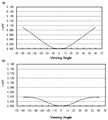
또한, 종래 표시패널에서 사용된 호스트A재료(Host A)와 본 발명의 실시예에 따른 표시패널에서 사용된 호스트B재료(Host B)를 기반으로 이들 간의 시야각 특성을 비교 실험한 결과 도 10과 같은 데이터를 얻었다. 도 10에서 가로축은 시야각(Viewing Angle)을 의미하고 세로축은 색도좌표에서의 색 편차(Δu'v')를 의미한다.In addition, the results of comparing and comparing the viewing angle characteristics between the host A material (Host A) used in the conventional display panel and the host B material (Host B) used in the display panel according to an embodiment of the present invention are shown in FIG. I got the same data. In FIG. 10, the horizontal axis represents the viewing angle, and the vertical axis represents the color deviation (Δu'v ') in the chromaticity coordinates.
표 1 및 도 10에 따르면, 종래 표시패널에서 사용된 호스트A재료(Host A)는 호스트 영역에서 생성된 EL 피크로 인해 노르스름한(yellowish) 색으로 변하면서 시야각 특성 및 효율이 저하되었다(도 10의 a 참조). 반면, 본 발명의 실시예에서 사용된 B호스트(Host B)는 MLCT1 영역에만 중첩되는 PL을 가지므로 호스트A재료(Host A) 대비 시야각 및 효율 특성이 향상되었다(도 10의 b 참조).According to Tables 1 and 10, the host A material (Host A) used in the conventional display panel was changed to a yellowish color due to the EL peak generated in the host area, and the viewing angle characteristics and efficiency were lowered (FIG. 10). See a). On the other hand, the B host (Host B) used in the embodiment of the present invention has PL that overlaps only in the MLCT1 region, thereby improving viewing angle and efficiency characteristics compared to Host A material (see FIG. 10B).
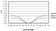
한편, 위의 설명에서는 호스트B재료(Host B)만을 이용한 하나의 실험 예를 기반으로 설명하였다. 하지만, 도 11에서 알 수 있는 바와 같이 이러한 특성은 호스트B재료(Host B)뿐만 아니라 호스트C 및 D재료(Host C, Host D)에서도 나타났다.Meanwhile, the above description has been described based on an example of an experiment using only Host B material. However, as can be seen in FIG. 11, this characteristic was found not only in the host B material (Host B) but also in the host C and D materials (Host C, Host D).
호스트B재료 내지 호스트D재료(Host B ~ Host D)를 이용하여 실험한 결과 색도좌표에서의 색 편차(Δu'v')는 대략 0.04 ~ 0.08 정도 나타났다. 호스트C 및 D재료(Host C, Host D) 또한 MLCT1 영역에만 중첩되는 PL을 가지고 있다. 호스트C 및 D재료(Host C, Host D)는 호스트A재료(Host A) 대비 시야각 및 효율 특성이 향상되었지만, 호스트B재료(Host B) 대비 시야각 및 효율 특성의 향상도가 다소 낮은 것으로 나타났다.As a result of experiments using Host B to Host D materials, the color deviation (Δu'v ') in the chromaticity coordinates was approximately 0.04 to 0.08. Host C and D materials (Host C and Host D) also have PLs that overlap only in the MLCT1 region. Host C and D materials (Host C and Host D) exhibited improved viewing angle and efficiency characteristics compared to Host A material, but showed little improvement in viewing angle and efficiency characteristics compared to Host B material (Host B).
이상 본 발명은 형광 재료의 호스트와 인광 재료의 도판트를 혼합하여 사용하고, 호스트 PL 영역을 인광 도판트 UV 흡수 영역 중 하나와 중첩하도록 제한하는 방식으로 호스트의 스펙트럼 영역을 최적화하여 시야각 특성 및 효율을 향상시킬 수 있는 효과가 있다.As described above, the present invention uses a mixture of a host of a fluorescent material and a dopant of a phosphorescent material, and optimizes the spectral region of the host by limiting the host PL region to overlap with one of the UV absorbing regions of the phosphorescent dopant to improve viewing angle characteristics and efficiency. It has the effect of improving.
이상 첨부된 도면을 참조하여 본 발명의 실시예를 설명하였지만, 상술한 본 발명의 기술적 구성은 본 발명이 속하는 기술 분야의 당업자가 본 발명의 그 기술적 사상이나 필수적 특징을 변경하지 않고서 다른 구체적인 형태로 실시될 수 있다는 것을 이해할 수 있을 것이다. 그러므로 이상에서 기술한 실시 예들은 모든 면에서 예시적인 것이며 한정적인 것이 아닌 것으로서 이해되어야 한다. 아울러, 본 발명의 범위는 상기 상세한 설명보다는 후술하는 특허청구범위에 의하여 나타내어진다. 또한, 특허청구범위의 의미 및 범위 그리고 그 등가 개념으로부터 도출되는 모든 변경 또는 변형된 형태가 본 발명의 범위에 포함되는 것으로 해석되어야 한다.
Although the embodiments of the present invention have been described above with reference to the accompanying drawings, the technical configuration of the present invention described above is in other specific forms without changing the technical spirit or essential features of the present invention by those skilled in the art to which the present invention pertains. It will be understood that it can be practiced. Therefore, the embodiments described above are to be understood in all respects as illustrative and not restrictive. In addition, the scope of the present invention is indicated by the claims below, rather than the detailed description. In addition, all modifications or variations derived from the meaning and scope of the claims and their equivalent concepts should be construed as being included in the scope of the present invention.
110a: 제1기판SP: 서브 픽셀(들)
T1: 스위칭 박막 트랜지스터Cst: 커패시터
T2: 구동 박막 트랜지스터150: 하부전극
160: 유기발광층170: 상부전극
H: 호스트 영역H+D: 혼합 영역
D: 도판트 영역Host PL: 호스트 PL 영역
Host A: 호스트A재료Host B: 호스트B재료
Host C: 호스트C재료Host D: 호스트D재료110a: first substrate SP: sub-pixel (s)
T1: Switching thin film transistor Cst: Capacitor
T2: driving thin film transistor 150: lower electrode
160: organic light emitting layer 170: upper electrode
H: host area H + D: mixed area
D: Dopant area Host PL: Host PL area
Host A: Host A material Host B: Host B material
Host C: Host C material Host D: Host D material
Claims (6)
Translated fromKorean상기 호스트는 형광 재료를 포함하고, 상기 도판트는 인광 재료를 포함하며,
상기 형광 재료의 호스트에 의한 호스트 PL 영역은 상기 인광 재료의 도판트에 의한 도판트 UV 흡수 영역 중 하나와 중첩하는 스펙트럼을 나타내되,
상기 호스트 PL 영역 내에는 상기 도판트 UV 흡수 영역의 MLCT1 영역이 존재하고, 상기 도판트 UV 흡수 영역의 MLCT3 영역은 일부만 존재하고,
상기 호스트 PL 영역은 상기 도판트 UV 흡수 영역의 MLCT1 영역의 피크와 중첩하고, 상기 도판트 UV 흡수 영역의 MLCT3 영역의 피크와 미중첩하고,
상기 호스트 PL 영역의 반치폭은 상기 도판트 UV 흡수 영역의 MLCT1 영역의 반치폭보다 좁고,
상기 호스트 PL 영역은 도판트 PL 영역과 일부 영역만 중첩하는 것을 특징으로 하는 유기전계발광표시장치.It is formed between two electrodes located on a substrate, a first host region including a host, a first mixed region in which the host and the dopant are mixed, a first dopant region including the dopant, and the dopant And a light emitting layer deposited in order of a second dopant region including, a second mixed region in which the host and the dopant are mixed, and a second host region including the host,
The host comprises a fluorescent material, the dopant comprises a phosphorescent material,
The host PL region by the host of the fluorescent material represents a spectrum overlapping with one of the dopant UV absorption regions by the dopant of the phosphor material,
In the host PL region, the MLCT1 region of the dopant UV absorption region is present, and the MLCT3 region of the dopant UV absorption region is only partially present,
The host PL region overlaps the peak of the MLCT1 region of the dopant UV absorption region, and does not overlap the peak of the MLCT3 region of the dopant UV absorption region,
The half width of the host PL region is narrower than that of the MLCT1 region of the dopant UV absorption region,
The host PL region overlaps the dopant PL region and only a portion of the organic light emitting display device.
Priority Applications (3)
| Application Number | Priority Date | Filing Date | Title |
|---|---|---|---|
| KR1020130148536AKR102088883B1 (en) | 2013-12-02 | 2013-12-02 | Organic Light Emitting Display Device |
| CN201410720926.8ACN104681591B (en) | 2013-12-02 | 2014-12-02 | Organic light-emitting display device |
| US14/557,679US20150155518A1 (en) | 2013-12-02 | 2014-12-02 | Organic light emitting display device |
Applications Claiming Priority (1)
| Application Number | Priority Date | Filing Date | Title |
|---|---|---|---|
| KR1020130148536AKR102088883B1 (en) | 2013-12-02 | 2013-12-02 | Organic Light Emitting Display Device |
Publications (2)
| Publication Number | Publication Date |
|---|---|
| KR20150064290A KR20150064290A (en) | 2015-06-11 |
| KR102088883B1true KR102088883B1 (en) | 2020-03-16 |
Family
ID=53266058
Family Applications (1)
| Application Number | Title | Priority Date | Filing Date |
|---|---|---|---|
| KR1020130148536AActiveKR102088883B1 (en) | 2013-12-02 | 2013-12-02 | Organic Light Emitting Display Device |
Country Status (3)
| Country | Link |
|---|---|
| US (1) | US20150155518A1 (en) |
| KR (1) | KR102088883B1 (en) |
| CN (1) | CN104681591B (en) |
Citations (1)
| Publication number | Priority date | Publication date | Assignee | Title |
|---|---|---|---|---|
| JP2012212879A (en)* | 2011-03-23 | 2012-11-01 | Semiconductor Energy Lab Co Ltd | Light-emitting element |
Family Cites Families (23)
| Publication number | Priority date | Publication date | Assignee | Title |
|---|---|---|---|---|
| TW463522B (en)* | 2000-11-07 | 2001-11-11 | Helix Technology Inc | Manufacturing method for organic light emitting diode |
| CN100495761C (en)* | 2004-06-03 | 2009-06-03 | 清华大学 | A kind of organic electroluminescent white light device and preparation method thereof |
| JP4667926B2 (en)* | 2005-03-30 | 2011-04-13 | 出光興産株式会社 | Aromatic amine derivative and organic electroluminescence device using the same |
| JP4956831B2 (en)* | 2006-03-09 | 2012-06-20 | 学校法人 中央大学 | Metal complex compound and organic electroluminescence device using the same |
| US7579773B2 (en)* | 2006-06-05 | 2009-08-25 | The Trustees Of Princeton University | Organic light-emitting device with a phosphor-sensitized fluorescent emission layer |
| KR100994114B1 (en)* | 2008-03-11 | 2010-11-12 | 삼성모바일디스플레이주식회사 | Thin Film Formation Method |
| KR101351410B1 (en)* | 2009-09-29 | 2014-01-14 | 엘지디스플레이 주식회사 | White Organic Light Emitting Device |
| US8664383B2 (en)* | 2010-10-15 | 2014-03-04 | Semiconductor Energy Laboratory Co., Ltd. | Organometallic complex, and light-emitting element and display device using the organometallic complex |
| KR101730554B1 (en)* | 2010-12-30 | 2017-04-26 | 엘지디스플레이 주식회사 | Organic electroluminescent device |
| DE112012000831C5 (en)* | 2011-02-16 | 2022-06-15 | Semiconductor Energy Laboratory Co., Ltd. | light emitting element |
| CN105932170B (en)* | 2011-02-16 | 2018-04-06 | 株式会社半导体能源研究所 | Light-emitting component |
| DE112012001504B4 (en)* | 2011-03-30 | 2017-09-21 | Semiconductor Energy Laboratory Co., Ltd. | Light-emitting element |
| CN103518270B (en)* | 2011-04-07 | 2016-04-06 | 株式会社半导体能源研究所 | Light-emitting element using phosphorescent compound and organic compound forming exciplex therefrom |
| KR101803537B1 (en)* | 2012-02-09 | 2017-11-30 | 가부시키가이샤 한도오따이 에네루기 켄큐쇼 | Light-emitting element |
| JP2013232629A (en)* | 2012-04-06 | 2013-11-14 | Semiconductor Energy Lab Co Ltd | Light-emitting element, light-emitting device, electronic device, and lighting device |
| JP6158542B2 (en)* | 2012-04-13 | 2017-07-05 | 株式会社半導体エネルギー研究所 | LIGHT EMITTING ELEMENT, LIGHT EMITTING DEVICE, ELECTRONIC DEVICE, AND LIGHTING DEVICE |
| JP6158543B2 (en)* | 2012-04-13 | 2017-07-05 | 株式会社半導体エネルギー研究所 | LIGHT EMITTING ELEMENT, LIGHT EMITTING DEVICE, ELECTRONIC DEVICE, AND LIGHTING DEVICE |
| KR20140038886A (en)* | 2012-09-21 | 2014-03-31 | 가부시키가이샤 한도오따이 에네루기 켄큐쇼 | Light-emitting element |
| KR102040874B1 (en)* | 2013-01-04 | 2019-11-06 | 삼성디스플레이 주식회사 | Silicon-based compound and organic light emitting diode comprising the same |
| WO2015037548A1 (en)* | 2013-09-12 | 2015-03-19 | Semiconductor Energy Laboratory Co., Ltd. | Organometallic iridium complex, light-emitting element, light-emitting device, electronic device, and lighting device |
| DE102014101650B4 (en)* | 2014-02-11 | 2021-07-08 | Pictiva Displays International Limited | Process for the production of an organic light-emitting diode and organic light-emitting diode |
| KR20160004458A (en)* | 2014-07-02 | 2016-01-13 | 삼성디스플레이 주식회사 | Organic Light Emitting Device |
| KR102344729B1 (en)* | 2014-12-15 | 2021-12-31 | 엘지디스플레이 주식회사 | Organic Light Emitting Display Device |
- 2013
- 2013-12-02KRKR1020130148536Apatent/KR102088883B1/enactiveActive
- 2014
- 2014-12-02CNCN201410720926.8Apatent/CN104681591B/enactiveActive
- 2014-12-02USUS14/557,679patent/US20150155518A1/ennot_activeAbandoned
Patent Citations (1)
| Publication number | Priority date | Publication date | Assignee | Title |
|---|---|---|---|---|
| JP2012212879A (en)* | 2011-03-23 | 2012-11-01 | Semiconductor Energy Lab Co Ltd | Light-emitting element |
Also Published As
| Publication number | Publication date |
|---|---|
| KR20150064290A (en) | 2015-06-11 |
| CN104681591B (en) | 2017-10-20 |
| US20150155518A1 (en) | 2015-06-04 |
| CN104681591A (en) | 2015-06-03 |
Similar Documents
| Publication | Publication Date | Title |
|---|---|---|
| US10332919B2 (en) | Organic light-emitting diode (OLED) array substrate and manufacturing method thereof and display device | |
| KR102525501B1 (en) | Organic light emitting display device | |
| US9905802B2 (en) | Organic light emitting display apparatus and method of manufacturing the same | |
| US10347858B2 (en) | White organic light emitting device | |
| US10158094B2 (en) | Organic light emitting diode and display device including the same | |
| US10056571B2 (en) | Organic light emitting display device | |
| KR102086404B1 (en) | Organic electroluminescent device, method of fabricating the same and organic electroluminescent display | |
| KR20150078389A (en) | Method for fabricating organic light emitting display device | |
| KR20160059563A (en) | Organice light emitting diode display | |
| KR20230152630A (en) | White organic light emitting device | |
| KR20160056705A (en) | White organic light emitting display device and method of fabricating the same | |
| KR102344729B1 (en) | Organic Light Emitting Display Device | |
| KR102650716B1 (en) | Display device and method for manufacturing the same | |
| JP5992495B2 (en) | Organic light emitting diode and organic light emitting diode display device | |
| CN221306433U (en) | Display substrate | |
| KR102410031B1 (en) | Organic light emitting diode, manufacturing method for the same, and organic light emitting display device having the organic light emitting diode | |
| US7656086B2 (en) | Organic light emitting diode display and method of manufacture thereof | |
| KR102088883B1 (en) | Organic Light Emitting Display Device | |
| KR20160090780A (en) | Organic Light Emitting Display Device | |
| US20230209924A1 (en) | Display device and display device production method | |
| KR20110053568A (en) | Organic light emitting display device | |
| US20240260325A1 (en) | Light emitting display device | |
| CN119836165A (en) | Display substrate and preparation method thereof | |
| KR20100059394A (en) | Organic light emitting diode and organic light emitting display device using the same |
Legal Events
| Date | Code | Title | Description |
|---|---|---|---|
| PA0109 | Patent application | Patent event code:PA01091R01D Comment text:Patent Application Patent event date:20131202 | |
| PG1501 | Laying open of application | ||
| PA0201 | Request for examination | Patent event code:PA02012R01D Patent event date:20180914 Comment text:Request for Examination of Application Patent event code:PA02011R01I Patent event date:20131202 Comment text:Patent Application | |
| E902 | Notification of reason for refusal | ||
| PE0902 | Notice of grounds for rejection | Comment text:Notification of reason for refusal Patent event date:20190818 Patent event code:PE09021S01D | |
| E701 | Decision to grant or registration of patent right | ||
| PE0701 | Decision of registration | Patent event code:PE07011S01D Comment text:Decision to Grant Registration Patent event date:20200225 | |
| GRNT | Written decision to grant | ||
| PR0701 | Registration of establishment | Comment text:Registration of Establishment Patent event date:20200309 Patent event code:PR07011E01D | |
| PR1002 | Payment of registration fee | Payment date:20200309 End annual number:3 Start annual number:1 | |
| PG1601 | Publication of registration | ||
| PR1001 | Payment of annual fee | Payment date:20230215 Start annual number:4 End annual number:4 | |
| PR1001 | Payment of annual fee | Payment date:20240215 Start annual number:5 End annual number:5 | |
| PR1001 | Payment of annual fee | Payment date:20250218 Start annual number:6 End annual number:6 |