KR102087933B1 - Light Emitting device and light emitting array - Google Patents
Light Emitting device and light emitting arrayDownload PDFInfo
- Publication number
- KR102087933B1 KR102087933B1KR1020120124381AKR20120124381AKR102087933B1KR 102087933 B1KR102087933 B1KR 102087933B1KR 1020120124381 AKR1020120124381 AKR 1020120124381AKR 20120124381 AKR20120124381 AKR 20120124381AKR 102087933 B1KR102087933 B1KR 102087933B1
- Authority
- KR
- South Korea
- Prior art keywords
- layer
- light emitting
- disposed
- electrode
- layers
- Prior art date
- Legal status (The legal status is an assumption and is not a legal conclusion. Google has not performed a legal analysis and makes no representation as to the accuracy of the status listed.)
- Active
Links
Images


Classifications
- H—ELECTRICITY
- H10—SEMICONDUCTOR DEVICES; ELECTRIC SOLID-STATE DEVICES NOT OTHERWISE PROVIDED FOR
- H10H—INORGANIC LIGHT-EMITTING SEMICONDUCTOR DEVICES HAVING POTENTIAL BARRIERS
- H10H20/00—Individual inorganic light-emitting semiconductor devices having potential barriers, e.g. light-emitting diodes [LED]
- H10H20/80—Constructional details
- H10H20/83—Electrodes
- H—ELECTRICITY
- H10—SEMICONDUCTOR DEVICES; ELECTRIC SOLID-STATE DEVICES NOT OTHERWISE PROVIDED FOR
- H10H—INORGANIC LIGHT-EMITTING SEMICONDUCTOR DEVICES HAVING POTENTIAL BARRIERS
- H10H29/00—Integrated devices, or assemblies of multiple devices, comprising at least one light-emitting semiconductor element covered by group H10H20/00
- H10H29/10—Integrated devices comprising at least one light-emitting semiconductor component covered by group H10H20/00
- H10H29/14—Integrated devices comprising at least one light-emitting semiconductor component covered by group H10H20/00 comprising multiple light-emitting semiconductor components
- H10H29/142—Two-dimensional arrangements, e.g. asymmetric LED layout
- H—ELECTRICITY
- H10—SEMICONDUCTOR DEVICES; ELECTRIC SOLID-STATE DEVICES NOT OTHERWISE PROVIDED FOR
- H10H—INORGANIC LIGHT-EMITTING SEMICONDUCTOR DEVICES HAVING POTENTIAL BARRIERS
- H10H20/00—Individual inorganic light-emitting semiconductor devices having potential barriers, e.g. light-emitting diodes [LED]
- H10H20/80—Constructional details
- H10H20/81—Bodies
- H10H20/811—Bodies having quantum effect structures or superlattices, e.g. tunnel junctions
- H10H20/812—Bodies having quantum effect structures or superlattices, e.g. tunnel junctions within the light-emitting regions, e.g. having quantum confinement structures
- H—ELECTRICITY
- H10—SEMICONDUCTOR DEVICES; ELECTRIC SOLID-STATE DEVICES NOT OTHERWISE PROVIDED FOR
- H10H—INORGANIC LIGHT-EMITTING SEMICONDUCTOR DEVICES HAVING POTENTIAL BARRIERS
- H10H20/00—Individual inorganic light-emitting semiconductor devices having potential barriers, e.g. light-emitting diodes [LED]
- H10H20/80—Constructional details
- H10H20/81—Bodies
- H10H20/814—Bodies having reflecting means, e.g. semiconductor Bragg reflectors
- H—ELECTRICITY
- H10—SEMICONDUCTOR DEVICES; ELECTRIC SOLID-STATE DEVICES NOT OTHERWISE PROVIDED FOR
- H10H—INORGANIC LIGHT-EMITTING SEMICONDUCTOR DEVICES HAVING POTENTIAL BARRIERS
- H10H20/00—Individual inorganic light-emitting semiconductor devices having potential barriers, e.g. light-emitting diodes [LED]
- H10H20/80—Constructional details
- H10H20/81—Bodies
- H10H20/816—Bodies having carrier transport control structures, e.g. highly-doped semiconductor layers or current-blocking structures
- H10H20/8162—Current-blocking structures
- H—ELECTRICITY
- H10—SEMICONDUCTOR DEVICES; ELECTRIC SOLID-STATE DEVICES NOT OTHERWISE PROVIDED FOR
- H10H—INORGANIC LIGHT-EMITTING SEMICONDUCTOR DEVICES HAVING POTENTIAL BARRIERS
- H10H20/00—Individual inorganic light-emitting semiconductor devices having potential barriers, e.g. light-emitting diodes [LED]
- H10H20/80—Constructional details
- H10H20/83—Electrodes
- H10H20/831—Electrodes characterised by their shape
- H—ELECTRICITY
- H10—SEMICONDUCTOR DEVICES; ELECTRIC SOLID-STATE DEVICES NOT OTHERWISE PROVIDED FOR
- H10H—INORGANIC LIGHT-EMITTING SEMICONDUCTOR DEVICES HAVING POTENTIAL BARRIERS
- H10H20/00—Individual inorganic light-emitting semiconductor devices having potential barriers, e.g. light-emitting diodes [LED]
- H10H20/80—Constructional details
- H10H20/83—Electrodes
- H10H20/832—Electrodes characterised by their material
- H—ELECTRICITY
- H10—SEMICONDUCTOR DEVICES; ELECTRIC SOLID-STATE DEVICES NOT OTHERWISE PROVIDED FOR
- H10H—INORGANIC LIGHT-EMITTING SEMICONDUCTOR DEVICES HAVING POTENTIAL BARRIERS
- H10H20/00—Individual inorganic light-emitting semiconductor devices having potential barriers, e.g. light-emitting diodes [LED]
- H10H20/80—Constructional details
- H10H20/84—Coatings, e.g. passivation layers or antireflective coatings
- H10H20/841—Reflective coatings, e.g. dielectric Bragg reflectors
- H—ELECTRICITY
- H10—SEMICONDUCTOR DEVICES; ELECTRIC SOLID-STATE DEVICES NOT OTHERWISE PROVIDED FOR
- H10H—INORGANIC LIGHT-EMITTING SEMICONDUCTOR DEVICES HAVING POTENTIAL BARRIERS
- H10H20/00—Individual inorganic light-emitting semiconductor devices having potential barriers, e.g. light-emitting diodes [LED]
- H10H20/80—Constructional details
- H10H20/85—Packages
- H10H20/857—Interconnections, e.g. lead-frames, bond wires or solder balls
- H—ELECTRICITY
- H01—ELECTRIC ELEMENTS
- H01L—SEMICONDUCTOR DEVICES NOT COVERED BY CLASS H10
- H01L2924/00—Indexing scheme for arrangements or methods for connecting or disconnecting semiconductor or solid-state bodies as covered by H01L24/00
- H01L2924/0001—Technical content checked by a classifier
- H01L2924/0002—Not covered by any one of groups H01L24/00, H01L24/00 and H01L2224/00
- H—ELECTRICITY
- H10—SEMICONDUCTOR DEVICES; ELECTRIC SOLID-STATE DEVICES NOT OTHERWISE PROVIDED FOR
- H10H—INORGANIC LIGHT-EMITTING SEMICONDUCTOR DEVICES HAVING POTENTIAL BARRIERS
- H10H20/00—Individual inorganic light-emitting semiconductor devices having potential barriers, e.g. light-emitting diodes [LED]
- H10H20/80—Constructional details
- H10H20/81—Bodies
- H10H20/822—Materials of the light-emitting regions
- H10H20/824—Materials of the light-emitting regions comprising only Group III-V materials, e.g. GaP
- H10H20/825—Materials of the light-emitting regions comprising only Group III-V materials, e.g. GaP containing nitrogen, e.g. GaN
Landscapes
- Led Devices (AREA)
- Led Device Packages (AREA)
Abstract
Translated fromKoreanDescription
Translated fromKorean실시예는 발광 소자 및 이를 포함하는 발광 소자 어레이에 관한 것이다.An embodiment relates to a light emitting device and a light emitting device array including the same.
질화갈륨(GaN)의 금속 유기화학기상 증착법 및 분자선 성장법 등의 발달을 바탕으로 고휘도 및 백색광 구현이 가능한 적색, 녹색 및 청색 발광 다이오드(LED:Light Emitting Diode)가 개발되었다.Based on the development of gallium nitride (GaN) metal organic chemical vapor deposition and molecular beam growth, red, green and blue light emitting diodes (LEDs) capable of realizing high luminance and white light have been developed.
이러한 LED는 백열등과 형광등 등의 기존 조명기구에 사용되는 수은(Hg)과 같은 환경 유해물질이 포함되어 있지 않아 우수한 친환경성을 가지며, 긴 수명, 저전력 소비특성 등과 같은 장점이 있기 때문에 기존의 광원들을 대체하고 있다. 이러한 LED 소자의 핵심 경쟁 요소는 고효율 및 고출력 칩 및 패키징 기술에 의한 고휘도의 구현이다.These LEDs do not contain environmentally harmful substances such as mercury (Hg) used in existing lighting fixtures such as incandescent lamps and fluorescent lamps, so they have excellent eco-friendliness, and have advantages such as long life and low power consumption characteristics. Is replacing it. The key competing element of these LED devices is the implementation of high efficiency and high brightness by high power chip and packaging technology.
고휘도를 구현하기 위해서 광 추출 효율을 높이는 것이 중요하다. 광 추출 효율을 높이기 위하여 플립 칩(flip-chip) 구조, 표면 요철 형성(surface texturing), 요철이 형성된 사파이어 기판(PSS:Patterned Sapphire Substrate), 광 결정(photonic crystal) 기술, 및 반사 방지막(anti-reflection layer) 구조 등을 이용한 다양한 방법들이 연구되고 있다.In order to realize high luminance, it is important to increase light extraction efficiency. Flip-chip structure, surface texturing, patterned sapphire substrate (PSS), photonic crystal technology, and anti-reflection film to improve light extraction efficiency Various methods using reflection layer structures have been studied.
일반적으로 발광 소자는 기판 위에 위치하는 제1 도전형 반도체층, 활성층 및 제2 도전형 반도체층을 포함하는 발광 구조물과, 제1 도전형 반도체층에 제1 전원을 공급하는 제1 전극층과, 제2 도전형 반도체층에 제2 전원을 공급하는 제2 전극층을 포함할 수 있다.In general, a light emitting device includes a light emitting structure including a first conductivity type semiconductor layer, an active layer and a second conductivity type semiconductor layer positioned on a substrate, a first electrode layer for supplying first power to the first conductivity type semiconductor layer, and It may include a second electrode layer for supplying a second power to the second conductivity-type semiconductor layer.
실시예는 수율을 향상시키고 개선된 발광 효율을 갖는 발광 소자 및 이를 포함하는 발광 소자 어레이를 제공한다.The embodiment provides a light emitting device having improved yield and improved luminous efficiency and a light emitting device array including the same.
실시예의 발광 소자는, 기판; 상기 기판 위에 배치된 서로 다른 도전형의 하부 및 상부 반도체층, 상기 하부 및 상부 반도체층 사이에 배치된 활성층을 갖는 발광 구조물; 및 상기 상부 반도체층 위에 배치된 제1 전극층을 포함하고, 상기 제1 전극층은 서로 중첩된 제1 접착층과 제1 본딩층을 포함하고, 상기 제1 접착층과 상기 제1 본딩층 사이에 반사층이 개재되지 않는다. 상기 제1 전극층은 상기 제1 접착층 위에 접하여 배치된 제1 배리어층을 더 포함할 수 있다.The light emitting device of the embodiment includes a substrate; A light emitting structure having lower and upper semiconductor layers of different conductivity types disposed on the substrate, and active layers disposed between the lower and upper semiconductor layers; And a first electrode layer disposed on the upper semiconductor layer, wherein the first electrode layer includes a first adhesive layer and a first bonding layer overlapping each other, and a reflective layer is interposed between the first adhesive layer and the first bonding layer. Does not work. The first electrode layer may further include a first barrier layer disposed in contact with the first adhesive layer.
상기 하부 도전형 반도체층 위에 배치된 제2 전극층을 더 포함하고, 상기 제2 전극층은 서로 중첩된 제2 접착층과 제2 본딩층을 포함하고, 상기 제2 접착층과 상기 제2 본딩층 사이에 반사층이 개재되지 않는다. 상기 제2 전극층은 상기 제2 접착층 위에 접하여 배치된 제2 배리어층을 더 포함할 수 있다.Further comprising a second electrode layer disposed on the lower conductive type semiconductor layer, the second electrode layer includes a second adhesive layer and a second bonding layer overlapping each other, a reflective layer between the second adhesive layer and the second bonding layer This is not interposed. The second electrode layer may further include a second barrier layer disposed in contact with the second adhesive layer.
상기 제1 또는 제2 접착층은 Cr, Rd 및 Ti 중 적어도 하나를 포함하고, 상기 제1 또는 제2 배리어층은 Ni, Cr, Ti 및 Pt 중 적어도 하나를 포함하고, 상기 제1 또는 제2 접착층의 두께는 적어도 5 ㎚ 내지 15 ㎚이고, 상기 하부 반도체층의 측면은 경사질 수 있다.The first or second adhesive layer includes at least one of Cr, Rd and Ti, and the first or second barrier layer includes at least one of Ni, Cr, Ti and Pt, and the first or second adhesive layer The thickness of at least 5 ㎚ to 15 ㎚, the side surface of the lower semiconductor layer may be inclined.
상기 발광 소자는 상기 상부 반도체층과 상기 제1 전극층 사이에 배치된 전도층을 더 포함하고, 상기 전도층과 상기 상부 반도체층 사이에 배치된 전류 차단층을 더 포함할 수 있다. 상기 전도층은 상기 전류 차단층의 상부와 측부를 감싸도록 배치될 수 있다.The light emitting device may further include a conductive layer disposed between the upper semiconductor layer and the first electrode layer, and may further include a current blocking layer disposed between the conductive layer and the upper semiconductor layer. The conductive layer may be disposed to surround the top and side of the current blocking layer.
상기 전류 차단층은 분산 브래그 반사층일 수 있다. 상기 분산 브래그 반사층은 굴절율이 서로 다른 제1 및 제2 층이 교대로 적어도 2회 이상 적층된 절연 물질을 포함할 수 있다. 상기 제1 전극층은 5 ㎛ 내지 100 ㎛의 폭을 가질 수 있다.The current blocking layer may be a distributed Bragg reflective layer. The dispersion Bragg reflective layer may include an insulating material in which first and second layers having different refractive indices are alternately stacked at least twice or more. The first electrode layer may have a width of 5 μm to 100 μm.
다른 실시예의 발광 소자 어레이는, 기판; 상기 기판 상에 수평 방향으로 서로 이격되어 배열된 복수의 발광 소자; 상기 복수의 발광 소자에서, 2개의 발광 소자를 연결하는 도전형 상호 연결층; 및 상기 복수의 발광 소자와 상기 도전형 상호 연결층 사이에 배치된 제1 절연층을 포함하고, 상기 복수의 발광 소자 각각은 서로 다른 도전형의 하부 및 상부 반도체층, 상기 하부 및 상부 반도체층 사이에 배치된 활성층을 갖는 발광 구조물; 상기 상부 반도체층 위에 배치된 제1 전극층; 및 상기 하부 반도체층 위에 배치된 제2 전극층을 포함하고, 상기 도전형 상호 연결층은 상기 2개의 발광 소자 중 하나의 상기 제1 전극층과 상기 2개의 발광 소자 중 다른 하나의 제2 전극층을 연결하고, 상기 제1 전극층은 서로 중첩된 제1 접착층과 제1 본딩층을 포함하고, 상기 제1 접착층과 상기 제1 본딩층 사이에 반사층이 개재되지 않는다. 상기 제1 전극층은 상기 제1 접착층 위에 접하여 배치된 제1 배리어층을 더 포함할 수 있다.In another embodiment, the light emitting device array includes a substrate; A plurality of light emitting elements arranged on the substrate spaced apart from each other in a horizontal direction; In the plurality of light emitting elements, a conductive interconnect layer connecting two light emitting elements; And a first insulating layer disposed between the plurality of light emitting elements and the conductive type interconnection layer, each of the plurality of light emitting elements being between lower and upper semiconductor layers of different conductivity types, and between the lower and upper semiconductor layers. A light emitting structure having an active layer disposed thereon; A first electrode layer disposed on the upper semiconductor layer; And a second electrode layer disposed on the lower semiconductor layer, the conductive interconnect layer connecting the first electrode layer of one of the two light emitting elements and the second electrode layer of the other of the two light emitting elements, , The first electrode layer includes a first adhesive layer and a first bonding layer overlapping each other, and a reflective layer is not interposed between the first adhesive layer and the first bonding layer. The first electrode layer may further include a first barrier layer disposed in contact with the first adhesive layer.
상기 제2 전극층은 서로 중첩된 제2 접착층과 제2 본딩층을 포함하고, 상기 제2 접착층과 상기 제2 본딩층 사이에 반사층이 개재되지 않는다. 상기 제2 전극층은 상기 제2 접착층 위에 접하여 배치된 제2 배리어층을 더 포함할 수 있다.The second electrode layer includes a second adhesive layer and a second bonding layer overlapping each other, and a reflective layer is not interposed between the second adhesive layer and the second bonding layer. The second electrode layer may further include a second barrier layer disposed in contact with the second adhesive layer.
상기 도전형 상호 연결층은 서로 중첩된 제3 접착층과 제3 본딩층을 포함하고, 상기 제3 접착층과 상기 제3 본딩층 사이에 반사층이 개재되지 않는다. 상기 도전형 상호 연결층은 상기 제3 접착층 위에 접하여 배치된 제3 배리어층을 더 포함할 수 있다. 상기 제1, 제2 또는 제3 접착층은 Cr, Rd 및 Ti 중 적어도 하나를 포함하고, 상기 제1, 제2 또는 제3 배리어층은 Ni, Ti, Cr 및 Pt 중 적어도 하나를 포함하고, 상기 제1, 제2 또는 제3 접착층의 두께는 적어도 5 ㎚ 내지 15 ㎚일 수 있다.The conductive interconnect layer includes a third adhesive layer and a third bonding layer overlapping each other, and a reflective layer is not interposed between the third adhesive layer and the third bonding layer. The conductive interconnect layer may further include a third barrier layer disposed in contact with the third adhesive layer. The first, second or third adhesive layer includes at least one of Cr, Rd and Ti, and the first, second or third barrier layer includes at least one of Ni, Ti, Cr and Pt, and The thickness of the first, second or third adhesive layer may be at least 5 nm to 15 nm.
발광 소자 어레이는 상기 제1 절연층과 상기 복수의 발광 소자 사이에 배치된 제2 절연층을 더 포함할 수 있다. 상기 제1 및 제2 절연층 중 적어도 하나는 분산 브래그 반사층일 수 있다.The light emitting element array may further include a second insulating layer disposed between the first insulating layer and the plurality of light emitting elements. At least one of the first and second insulating layers may be a distributed Bragg reflective layer.
상기 도전형 상호 연결층에 의해 연결된 상기 2개의 발광 소자의 제1 및 제2 전극층 및 상기 도전형 상호 연결층은 일체일 수 있다.The first and second electrode layers of the two light emitting devices connected by the conductive interconnect layer and the conductive interconnect layer may be integral.
상기 도전형 상호 연결층의 두께는 상기 제1 전극층의 두께보다 더 두꺼울 수 있다. 상기 발광 소자 각각은 상기 상부 반도체층과 상기 제1 전극층 사이에 배치된 전도층을 더 포함할 수 있고, 상기 발광 구조물과 상기 제1 전극층의 사이에 상기 제1 절연층과 이격되어 배치된 전류 차단층을 더 포함할 수 있다. 상기 제1 전극층은 상기 전류 차단층의 상부와 측부를 감싸도록 배치되고, 상기 전류 차단층은 분산 브래그 반사층일 수 있다. 상기 제1 전극층은 5 ㎛ 내지 100 ㎛의 폭을 갖고, 복수의 발광 소자는 상기 도전형 상호 연결층에 의해 서로 직렬 연결될 수 있다.The thickness of the conductive interconnect layer may be thicker than that of the first electrode layer. Each of the light emitting devices may further include a conductive layer disposed between the upper semiconductor layer and the first electrode layer, and block current disposed spaced apart from the first insulating layer between the light emitting structure and the first electrode layer. It may further include a layer. The first electrode layer is disposed to surround the top and side of the current blocking layer, and the current blocking layer may be a distributed Bragg reflective layer. The first electrode layer has a width of 5 μm to 100 μm, and a plurality of light emitting devices may be connected to each other in series by the conductive interconnect layer.
실시예에 따른 발광 소자 및 이를 포함하는 발광 소자 어레이는 전극층과 도전형 상호 연결층에서, 본딩층과 접착층 사이에 반사층을 개재시키지 않아 접착층을 두껍게 형성할 수 있기 때문에, 전극층과 발광 구조물의 잡착력을 강화시키고 도전형 상호 연결층과 절연층의 접착력을 강화시킴으로써, 기존의 얇은 접착층으로 인해 제품의 불량이 발생하여 수율이 감소하는 문제를 해결할 수 있고, 절연층 대신에 분산 브래그 반사층을 배치하여 반사층의 역할을 대신 수행할 수 있도록 함으로써 발광 효율을 개선시킬 수 있다.Since the light emitting device according to the embodiment and the light emitting device array including the same can form a thick adhesive layer without interposing a reflective layer between the bonding layer and the adhesive layer in the electrode layer and the conductive type interconnection layer, the adhesion force between the electrode layer and the light emitting structure By strengthening and strengthening the adhesive strength of the conductive interconnect layer and the insulating layer, it is possible to solve the problem that the yield decreases due to defects in the product due to the existing thin adhesive layer, and a reflective Bragg reflective layer is disposed instead of the insulating layer to form the reflective layer. It is possible to improve the luminous efficiency by allowing to perform the role of.
도 1은 실시예에 의한 발광 소자의 단면도를 나타낸다.
도 2a 내지 도 2f는 도 1의 "A" 부분의 실시예들을 나타내는 도면이다.
도 3은 실시예에 의한 발광 소자를 이용한 발광 소자 어레이의 단면도를 나타낸다.
도 4는 다른 실시예의 발광 소자 어레이의 단면도를 나타낸다.
도 5는 또 다른 실시예에 의한 발광 소자 어레이의 단면도를 나타낸다.
도 6은 또 다른 실시예의 발광 소자 어레이의 단면도를 나타낸다.
도 7은 또 다른 실시예에 따른 발광 소자 어레이의 평면도를 나타낸다.
도 8은 도 7에 도시된 발광 소자 어레이의 8-8'선을 따라 절개한 단면도를 나타낸다.
도 9는 도 7에 도시된 발광 소자 어레이의 9-9'선을 따라 절개한 단면도를 나타낸다.
도 10은 도 7에 도시된 발광 소자 어레이의 10-10'선을 따라 절개한 단면도를 나타낸다.
도 11은 도 7에 도시된 발광 소자 어레이의 11-11'선을 따라 절개한 단면도를 나타낸다.
도 12는 도 7에 도시된 발광 소자 어레이의 회로도를 나타낸다.
도 13은 또 다른 실시예에 따른 발광 소자를 포함하는 발광 소자 어레이의 단면도를 나타낸다.
도 14는 실시 예에 따른 발광 소자 패키지를 포함하는 조명 장치의 분해 사시도이다.
도 15는 실시 예에 따른 발광 소자 패키지를 포함하는 표시 장치를 나타낸다.1 is a sectional view showing a light emitting device according to an embodiment.
2A to 2F are diagrams illustrating embodiments of the “A” portion of FIG. 1.
3 is a sectional view showing a light emitting device array using a light emitting device according to an embodiment.
4 is a sectional view showing a light emitting device array according to another embodiment.
5 is a sectional view showing a light emitting device array according to another embodiment.
6 shows a cross-sectional view of another embodiment of a light emitting device array.
7 is a plan view of a light emitting device array according to another embodiment.
8 is a cross-sectional view taken along line 8-8 'of the light emitting device array shown in FIG. 7.
9 is a cross-sectional view taken along line 9-9 'of the light emitting device array shown in FIG. 7.
10 is a sectional view taken along line 10-10 'of the light emitting device array shown in FIG. 7.
11 is a cross-sectional view taken along line 11-11 'of the light emitting device array shown in FIG. 7.
12 shows a circuit diagram of the light emitting device array shown in FIG. 7.
13 is a sectional view showing a light emitting device array including a light emitting device according to another embodiment.
14 is an exploded perspective view of a lighting device including a light emitting device package according to an embodiment.
15 illustrates a display device including a light emitting device package according to an embodiment.
이하, 본 발명을 구체적으로 설명하기 위해 실시예를 들어 설명하고, 발명에 대한 이해를 돕기 위해 첨부도면을 참조하여 상세하게 설명하기로 한다. 그러나, 본 발명에 따른 실시예들은 여러 가지 다른 형태로 변형될 수 있으며, 본 발명의 범위가 아래에서 상술하는 실시예들에 한정되는 것으로 해석되지 않아야 한다. 본 발명의 실시예들은 당 업계에서 평균적인 지식을 가진 자에게 본 발명을 보다 완전하게 설명하기 위해서 제공되는 것이다.Hereinafter, examples will be described to specifically describe the present invention, and in order to help understanding of the present invention, it will be described in detail with reference to the accompanying drawings. However, the embodiments according to the present invention may be modified in various other forms, and the scope of the present invention should not be construed as being limited to the embodiments described below. The embodiments of the present invention are provided to more fully describe the present invention to those skilled in the art.
본 발명에 따른 실시 예의 설명에 있어서, 각 element의 " 상(위)" 또는 "하(아래)(on or under)"에 형성되는 것으로 기재되는 경우에 있어, 상(위) 또는 하(아래)(on or under)는 두개의 element가 서로 직접(directly)접촉되거나 하나 이상의 다른 element가 상기 두 element사이에 배치되어(indirectly) 형성되는 것을 모두 포함한다. 또한 “상(위)" 또는 "하(아래)(on or under)”로 표현되는 경우 하나의 element를 기준으로 위쪽 방향뿐만 아니라 아래쪽 방향의 의미도 포함할 수 있다.In the description of the embodiment according to the present invention, in the case of being described as being formed on the "top (top)" or "bottom (bottom) (on or under)" of each element, the top (top) or bottom (bottom) (on or under) includes both two elements directly contacting each other or one or more other elements formed indirectly between the two elements. In addition, when expressed as “up (up)” or “down (down)” (on or under), it may include the meaning of the downward direction as well as the upward direction based on one element.
도면에서 각층의 두께나 크기는 설명의 편의 및 명확성을 위하여 과장되거나 생략되거나 또는 개략적으로 도시되었다. 또한 각 구성요소의 크기는 실제크기를 전적으로 반영하는 것은 아니다.In the drawings, the thickness or size of each layer is exaggerated, omitted, or schematically illustrated for convenience and clarity. Also, the size of each component does not entirely reflect the actual size.
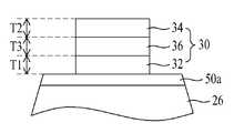
도 1은 실시예에 의한 발광 소자(100)의 단면도를 나타낸다.1 is a sectional view showing a
도 1에 예시된 발광 소자(100)는 기판(10), 버퍼층(12), 발광 구조물(20), 제1 및 제2 전극층(30, 40) 및 도전층(50a)을 포함한다.The
기판(10)은 반도체 물질 성장에 적합한 물질, 캐리어 웨이퍼로 형성될 수 있다. 또한 기판(10)은 열 전도성이 뛰어난 물질로 형성될 수 있으며, 전도성 기판 또는 절연성 기판일 수 있다. 또한, 기판(10)은 투광성을 갖는 물질로 이루어질 수도 있으며, 전체 질화물 발광 구조물(20)의 휨을 가져오지 않으면서, 스크라이빙(scribing) 공정 및 브레이킹(breading) 공정을 통해 별개의 칩으로 잘 분리시키기 위한 정도의 기계적 강도를 가질 수 있다. 예를 들어 기판(10)은 사파이어(Al203), GaN, SiC, ZnO, Si, GaP, InP, Ga203, GaAs, Ge 중 적어도 하나를 포함하는 물질일 수 있다. 이러한 기판(10)의 상면에는 요철 패턴이 형성될 수 있다.The
버퍼층(12)은 기판(10)과 발광 구조물(20) 사이에 배치되며, Ⅲ-Ⅴ족 원소의 화합물 반도체를 이용하여 형성될 수 있다. 버퍼층(12)은 기판(10)과 발광 구조물(20) 사이의 격자 상수의 차이를 줄여주는 역할을 한다. 예를 들어, 버퍼층(12)은 AlN을 포함하거나 언 도프드(undoped) 질화물을 포함할 수 있으나, 이에 한정되지는 않는다. 버퍼층(12)은 기판(10)의 종류와 발광 구조물(20)의 종류에 따라 생략될 수도 있다.The
발광 구조물(20)은 버퍼층(12)의 상부에 순차적으로 배치된 하부 반도체층(22), 활성층(24) 및 상부 반도체층(24)을 포함한다. 하부 반도체층(22)과 상부 반도체층(26)은 서로 다른 도전형을 가질 수 있다.The
하부 반도체층(22)은 버퍼층(12)과 활성층(24) 사이에 배치되며, 반도체 화합물을 포함할 수 있으며, Ⅲ-Ⅴ족, Ⅱ-Ⅵ족 등의 화합물 반도체로 구현될 수 있으며, 제1 도전형 도펀트가 도핑될 수 있다. 예를 들어, 햐부 반도체층(22)은 AlxInyGa(1-x-y)N (0≤x≤1, 0≤y≤1, 0≤x+y≤1)의 조성식을 갖는 반도체 물질, InAlGaN, AlGaAs, GaP, GaAs, GaAsP, AlGaInP 중 어느 하나 이상을 포함할 수 있다. 하부 반도체층(22)은 제1 도전형의 반도체층일 수 있다. 만일, 하부 반도체층(22)이 n형 반도체층인 경우, 제1 도전형 도펀트는 Si, Ge, Sn, Se, Te 등과 같은 n형 도펀트를 포함할 수 있다. 하부 반도체층(22)은 단층 또는 다층 구조를 가질 수 있으며, 이에 대해 한정하지는 않는다.The lower semiconductor layer 22 is disposed between the
활성층(24)은 하부 반도체층(22)과 상부 반도체층(26) 사이에 배치되며, 단일 우물 구조(Double Hetero Structure), 다중 우물 구조, 단일 양자 우물 구조, 다중 양자 우물(MQW:Multi Quantum Well) 구조, 양자점 구조 또는 양자선 구조 중 어느 하나를 포함할 수 있다. 활성층(24)은 Ⅲ-Ⅴ족 원소의 화합물 반도체 재료를 이용하여 우물층과 장벽층, 예를 들면 InGaN/GaN, InGaN/InGaN, GaN/AlGaN, InAlGaN/GaN, GaAs(InGaAs),/AlGaAs, GaP(InGaP)/AlGaP 중 어느 하나 이상의 페어 구조를 가질 수 있으나 이에 한정되지는 않는다. 우물층은 장벽층의 에너지 밴드 갭보다 작은 에너지 밴드 갭을 갖는 물질로 이루어질 수 있다.The
상부 반도체층(26)은 활성층(24)의 상부에 배치되며, 반도체 화합물을 포함할 수 있다. 상부 반도체층(26)은 Ⅲ-Ⅴ족, Ⅱ-Ⅵ족 등의 화합물 반도체로 구현될 수 있으며, 예를 들어 InxAlyGa1-x-yN (0≤x≤1, 0≤y≤1, 0≤x+y≤1)의 조성식을 갖는 반도체 물질 또는 AlInN, AlGaAs, GaP, GaAs, GaAsP, AlGaInP 중 어느 하나 이상을 포함할 수 있다.The
제1 도전형 반도체층인 하부 반도체층(22)과 달리 상부 반도체층(26)은 제2 도전형 반도체층일 수 있으며, 제2 도전형 도펀트가 도핑될 수 있다. 상부 반도체층(26)이 p형 반도체층인 경우, 제2 도전형 도펀트는 Mg, Zn, Ca, Sr, Ba 등과 같은 p형 도펀트일 수 있다. 상부 반도체층(26)은 단층 또는 다층 구조를 가질 수 있으며, 이에 대해 한정하지는 않는다.Unlike the lower semiconductor layer 22 which is the first conductivity type semiconductor layer, the
하부 반도체층(22)은 n형 반도체층이고, 상부 반도체층(26)은 p형 반도체층으로 구현될 수 있으며, 이에 따라 발광 구조물(20)은 N-P 접합, P-N 접합, N-P-N 접합, 및 P-N-P 접합 구조 중 적어도 하나를 포함할 수 있다.The lower semiconductor layer 22 is an n-type semiconductor layer, and the
한편, 제1 전극층(30)은 상부 반도체층(26) 위에 배치되고, 제2 전극층(40)은 하부 반도체층(22) 위에 배치된다. 제2 전극층(40)을 하부 반도체층(22) 위에 배치하기 위해, 발광 구조물(20)은 하부 반도체층(22) 일부를 노출할 수 있다. 즉, 상부 반도체층(26), 활성층(24) 및 하부 반도체층(22)의 일부가 메사 식각(mesa etching)에 의하여 식각되어 하부 반도체층(22)의 일부를 노출할 수 있다. 이때, 하부 반도체층(22)의 노출면은 활성층(24)의 하면보다 낮게 위치할 수 있다.Meanwhile, the
도 2a 내지 도 2f는 도 1의 "A" 부분의 실시예들을 나타내는 도면이다.2A to 2F are diagrams illustrating embodiments of the “A” portion of FIG. 1.
도 2a를 참조하면, 실시예의 제1 전극층(30)은 서로 중첩된 제1 접착층(32) 및 제1 본딩층(34)을 포함할 수 있다. 즉, 제1 접착층(32)은 상부 반도체층(26)의 위에 배치되고, 제 본딩층(34)은 제1 접착층(32)의 위에 배치될 수 있다. 이때, 제1 접착층(32)과 제1 본딩층(34) 사이에 반사층이 개재되지 않는다. 즉, 제1 전극층(30)은 반사층을 포함하지 않는다.2A, the
제1 접착층(32)은 상부 반도체층(26)과 오믹 접촉하는 물질을 포함할 수 있다. 예를 들어, 제1 접착층(32)은 Cr, Rd 및 Ti 중 적어도 하나의 재료로, 단층 또는 다층 구조로 형성될 수 있다. 또한, 제1 접착층(32)의 두께(T1)는 적어도 5 ㎚ 내지 15 ㎚일 수 있다. 예를 들어, 제1 접착층(32)은 2 ㎚ 내지 10 ㎛의 두께(T1)를 가질 수 있다.The first
또한, 제1 본딩층(34)은 제1 접착층(32)에 접하여 배치될 수도 있지만, 후술되는 바와 같이 제1 배리어층(36)이 개재될 경우 제1 접착층(32)에 접하지 않고 그(32)의 상부에 배치될 수도 있다. 제1 본딩층(34)은 Au을 포함할 수 있고, 100 ㎚ 내지 180 ㎚의 두께(T2) 예를 들어, 140 ㎚의 두께를 가질 수 있다.Further, the
제1 전극층(30)은 5 ㎛ 내지 100 ㎛의 폭(W1)을 가질 수도 있다.The
다른 실시예에 의하면, 도 2b에 예시된 바와 같이, 제1 전극층(30)은 제1 접착층(32)과 제1 본딩층(34) 사이에 배치된 제1 배리어층(36)을 더 포함할 수 있다. 제1 배리어층(36)은 제1 접착층(32)과 제1 본딩층(34)에 각각 접하여 배치될 수 있다.According to another embodiment, as illustrated in FIG. 2B, the
제1 배리어층(36)은 Ni, Cr, Ti 및 Pt 중 적어도 하나를 포함하는 재료로, 단층 또는 다층으로 형성될 수 있다. 예를 들어, 제1 배리어층(36)은 Cr과 Pt의 합금으로 이루어질 수 있다. 또한, 제1 배리어층(36)은 200 ㎚ 내지 300 ㎚ 예를 들어, 250 ㎚의 두께(T3)를 가질 수 있다.The
도 1에 도시된 하부 반도체층(22)의 위에 배치된 제2 전극층(40)은 서로 중첩된 제2 접착층과 제2 본딩층을 포함할 수 있다. 제2 접착층은 Cr, Rd 및 Ti 중 적어도 하나의 재료로, 단층 또는 다층 구조로 형성될 수 있고, 제2 본딩층은 Au을 포함할 수 있다.The
제2 접착층 및 제2 본딩층은 제1 접착층(32) 및 제2 본딩층(34)과 동일한 구조 및 동일한 물질로 이루어질 수 있지만, 이에 국한되지 않는다. 즉, 제2 전극층(40)은 제1 전극층(30)과 마찬가지로 제2 접착층과 제2 본딩층 사이에 반사층이 개재되지 않을 수도 있지만, 제2 접착층과 제2 본딩층 사이에 반사층이 개재될 수도 있다. 또한, 제2 전극층(40)은 제1 전극층(30)과 서로 다른 구성 및 물질을 가질 수 있다. 즉, 제2 전극층(40)은 제2 접착층과 제2 본딩층으로 구성되고, 제1 전극층(30)은 제1 접착층(32), 제1 배리어층(36) 및 제1 본딩층(34)으로 구성될 수도 있다.The second adhesive layer and the second bonding layer may be made of the same structure and the same material as the first
또한, 제2 전극층(40)은 제2 접착층과 제2 본딩층 사이에 배치된 제2 배리어층을 더 포함할 수 있다. 제2 배리어층은 제2 접착층 및 제2 본딩층과 각각 접하여 배치될 수 있다. 제2 배리어층은 Ni, Cr, Ti 및 Pt 중 적어도 하나를 포함하는 재료로, 단층 또는 다층으로 형성될 수 있다.In addition, the
제2 배리어층은 제1 배리어층(36)과 동일한 물질로 이루어질 수 있지만, 이에 국한되지 않는다. 즉, 도 2b에 도시된 바와 같이, 제2 배리어층은 제1 배리어층(36)이 제1 접착층(32)과 제1 본딩층(36) 사이에 개재된 모습과 동일한 모습으로 제2 접착층과 제2 본딩층 사이에 배치될 수 있다. 또는, 제2 배리어층은 제1 배리어층(36)과 다른 두께 및 다른 물질로 이루어질 수도 있다.The second barrier layer may be made of the same material as the
예를 들어, 제2 전극층(40)이 제2 접착층, 제2 배리어층 및 제2 본딩층으로 이루어지고, 제1 전극층(30)은 제1 접착층(32) 및 제1 본딩층(34)으로 이루어질 수도 있다.For example, the
또한, 도 1에 도시된 바와 같이, 하부 반도체층(22)의 측면은 기판(10)에 대해 경사각(θ1)으로 경사지고, 노출된 하부 반도체층(22)에 인접한 측면은 경사각(θ2)으로 경사질 수도 있다. 경사각(θ1, θ2)은 30° 내지 80°일 수 있다. 이와 같이, 하부 반도체층(22)의 측면이 경사져 있을 경우, 활성층(24)에서 방출된 광의 추출 효율이 향상될 수 있다. 그러나, 경사각(θ1, θ2)이 30°보다 작을 경우, 활성층(24)의 영역이 감소되어 발광 효율이 저하될 수 있고, 80° 보다 클 경우, 광 추출 효율을 기대할 수 없을 수도 있다. 따라서, 경사각(θ1, θ2)은 30° 내지 80°의 예를 들어, 70°일 수 있다.In addition, as shown in FIG. 1, the side surface of the lower semiconductor layer 22 is inclined at an inclination angle θ1 with respect to the
만일, 제1 접착층(32)과 제1 배리어층(36) 사이에 반사층이 개재될 경우, 반사층은 활성층(24)에서 방출된 광을 반사시켜 제1 전극층(30)의 금속에 의해 흡수되는 광량을 줄일 수 있다. 그러나, 반사층이 제1 접착층(32)과 제1 배리어층(36) 사이에 개재될 경우, Au로 이루어진 제1 본딩층(34)과 Al로 이루어진 반사층이 Ni로 이루어진 제1 배리어층(36)을 사이에 두고 서로 상호 확산(inter-diffusion)될 수 있는 문제점이 있다.If, when the reflective layer is interposed between the first
또한, 충분한 반사도를 얻기 위해, 반사층은 통상 50 ㎚ 내지 300 ㎚의 두께로 형성될 수 있다. 이러한 두꺼운 반사층의 존재로 인해, 제1 접착층(32)이 예를 들면 2 ㎚ 보다 얇은 두께로 형성되어, 제1 전극층(30)과 발광 구조물(20) 사이에 접착력이 저하될 수 있다.In addition, in order to obtain sufficient reflectivity, the reflective layer can be usually formed to a thickness of 50 nm to 300 nm. Due to the presence of such a thick reflective layer, the first
그러나, 본 실시예에 의하면, 제1 접착층(32)과 제1 본딩층(34) 사이에 반사층이 개재되지 않는다. 또한, 제2 접착층과 제2 본딩층 사이에 반사층이 개재되지 않는다. 따라서, 반사층이 개재되지 않는 두께만큼 제1 접착층(32)이 두껍게 형성될 수 있어, 제1 전극층(30)과 발광 구조물(20) 사이의 접착력을 향상시킬 수 있고, 반사층과 제1 본딩층(34) 간의 상호 확산이 발생할 염려도 제거될 수 있다. 따라서, 전술한 바와 같이, 실시예에 의하면, 제1 접착층(32)은 2 ㎚ 이상의 두꺼운 두께(T1)를 가질 수 있다.However, according to this embodiment, a reflective layer is not interposed between the first
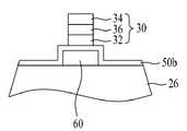
또한, 발광 소자는 도 1에 예시된 바와 같이, 상부 반도체층(26)과 제1 전극층(30) 사이에 배치된 전도층(50a)을 더 포함할 수 있다. 도 1에서 전도층(50a)은 상부 반도체층(26) 위에 배치되지만 이에 국한되지 않고 다양한 형태로 배치될 수 있다. 예를 들어, 도 2c 및 도 2d를 참조하면, 전도층(50b)은 전류 차단층(60)의 상부와 측부를 감싸도록 배치될 수 있다.In addition, as illustrated in FIG. 1, the light emitting device may further include a
전도층(50a, 50b)은 전반사를 감소시킬 뿐만 아니라, 투광성이 좋기 때문에 활성층(24)으로부터 방출되어 상부 반도체층(26)을 거친 빛의 추출 효율을 증가시킬 수 있다. 전도층(50a, 50b)은 발광 파장에 대해 투과율이 높은 투명한 산화물계 물질, 예컨대, ITO(Indium Tin Oxide), TO(Tin Oxide), IZO(Indium Zinc Oxide), IZTO(Indium Zinc Tin Oxide), IAZO(Indium Aluminium Zinc Oxide), IGZO(Indium Gallium Zinc Oxide), IGTO(Indium Gallium Tin Oxide), AZO(Aluminium Zinc Oxide), ATO(Aluminium Tin Oxide), GZO(Gallium Zinc Oxide), IrOx, RuOx, RuOx/ITO, Ni, Ag, Ni/IrOx/Au 또는 Ni/IrOx/Au/ITO 중 하나 이상을 이용하여 단층 또는 다층으로 구현할 수 있다.The
또한, 실시예에 의한 발광 소자는 도 2c 내지 도 2f에 예시된 바와 같이, 제1 전극층(30)과 상부 반도체층(26) 사이에 배치된 전류 차단층(60)을 더 포함할 수 있다. 전류 차단층(60)은 제1 전극층(30)으로부터 활성층(24)으로 향하는 캐리어가 적절히 확산되도록 하여 활성층(22)의 광도 향상에 기여할 수 있다.In addition, the light emitting device according to the embodiment may further include a
전류 차단층(60)은 실리콘 옥사이드(SiO2)와 같은 물질로 형성되거나 공기(air)에 의한 공동 형태로 형성될 수 있다. 또는, 도 2c에 예시된 바와 같이, 전류 차단층(60)은 분산 브래그 반사층(DBR:Distributed Bragg Reflector)(이하, ;제1 분산 브래그 반사층' 이라 함)(60a, 60b)으로 구현될 수도 있다. 분산 브래그 반사층이란, 굴절율이 서로 다른 둘 이상의 절연층이 교번하여 다수 층으로 적층되어 생성됨에 따라 반사율을 높이는 층을 의미한다. 도 2c에 예시된 제1 분산 브래그 반사층(60a, 60b)은 제1 접착층(32)과 제1 본딩층(34) 사이에 개재되지 않는 반사층의 역할과 전류 차단층(60)의 역할을 동시에 수행할 수 있다. 제1 분산 브래그 반사층(60a, 60b)은 90% 이하의 반사율을 갖는 반사층보다 더 높은 반사율 예를 들어, 98%의 반사율을 갖기 때문에 반사층의 역할을 보다 우수하게 수행할 수 있다.The
도 2c의 경우, 굴절율이 서로 다른 제1 층(62a, 62b) 및 제2 층(64a, 64b)이 교대로 2회 적층된 모습을 나타내지만, 2회보다 더 많은 횟수로 적층될 수 있다.In the case of FIG. 2C, the
제1 층(62a, 62b)은 저굴절율층으로서, 예를 들어 1.4의 굴절율을 갖는 실리콘 산화물(SiO2) 또는 1.6의 굴절율을 갖는 알루미늄 산화물(Al2O3)로 이루어질 수 있다. 또한, 제2 층(64a, 64b)은 고굴절율층으로서, 예를 들어, 2.05 내지 2.25의 굴절율을 갖는 실리콘 질화물(Si3N4), 2 이상의 굴절율을 갖는 티타늄질화물(TiO2), 또는 3 이상의 굴절율을 갖는 Si-H으로 이루어질 수 있다.The
또한, 제1 분산 브래그 반사층(60a, 60b)에서 제1 층(62a, 62b)과 제2 층(64a, 64b) 각각은 λ/(4n)의 두께를 가질 수 있다. 여기서, λ은 활성층(24)에서 방출된 광의 파장을 나타내고, n은 해당 층의 굴절율을 나타낸다.In addition, each of the
도 2c를 참조하면, DBR로 구현되는 전류 차단층(60)의 폭(W2)은 제1 전극층(30)의 폭(W1)의 1 내지 10배가 될 수 있다.Referring to FIG. 2C, the width W2 of the
이하, 전술한 발광 소자를 여러 개 이용하여 빛을 발하는 반도체 소자 어레이에 대해 첨부된 도면을 참조하여 다음과 같이 살펴본다.Hereinafter, a semiconductor device array emitting light using a plurality of the above-described light emitting devices will be described with reference to the accompanying drawings.
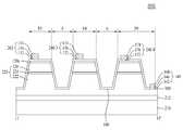
도 3은 실시예에 의한 발광 소자를 이용한 발광 소자 어레이(200A)의 단면도를 나타낸다.3 is a sectional view showing a light emitting
도 3에 예시된 발광 소자 어레이(200A)는 기판(210), 복수의 발광 소자(D1, D2), 도전형 상호 연결층(conductive interconnection layer)(170) 및 제1 절연층(180)을 포함한다.The light emitting
기판(210)은 반도체 물질 성장에 적합한 물질, 캐리어 웨이퍼로 형성될 수 있다. 또한 기판(210)은 열 전도성이 뛰어난 물질로 형성될 수 있으며, 전도성 기판 또는 절연성 기판일 수 있다. 또한, 기판(210)은 투광성을 갖는 물질로 이루어질 수도 있으며, 발광 소자(D1, D2) 각각의 질화물 발광 구조물(220a, 220b) 전체의 휨을 가져오지 않을 정도의 기계적 강도를 갖는 물질로 이루어질 수 있다. 예를 들어 기판(210)은 사파이어(Al203), GaN, SiC, ZnO, Si, GaP, InP, Ga203, GaAs, Ge 중 적어도 하나를 포함하는 물질일 수 있다. 이러한 기판(210)의 상면에는 요철 패턴이 형성될 수 있다.The
복수의 발광 소자(예를 들어, D1, D2)는 기판(210) 상에 수평 방향으로 서로 이격되어 배열된다. 도 3의 경우, 설명의 편의상 2개의 발광 소자(D1, D2)만이 도시되어 있지만, 2개보다 더 많은 수의 발광 소자가 도 3에 도시된 바와 같이 형태로 기판(210) 상에 배열될 수 있다.The plurality of light emitting elements (eg, D1 and D2) are arranged on the
복수의 발광 소자(D1, D2) 각각은 도 1에 예시된 바와 같은 구조를 갖는다. 즉, 제1 발광 소자(D1)는 발광 구조물(220a), 제1 전극층(130a) 및 제2 전극층(140a)을 포함하고, 제2 발광 소자(D2)는 발광 구조물(220b), 제1 전극층(130b) 및 제2 전극층(140b)을 포함한다. 발광 구조물(220a, 220b)은 도 1에 예시된 발광 구조물(20)과 동일하다. 즉, 발광 구조물(220a)은 서로 다른 도전형의 하부 및 상부 반도체층(222a, 226a)과 하부 및 상부 반도체층(222a, 226a) 사이에 배치된 활성층(224a)을 갖고, 발광 구조물(220b)은 서로 다른 도전형의 하부 및 상부 반도체층(222b, 226b)과 하부 및 상부 반도체층(222b, 226b) 사이에 배치된 활성층(224b)을 갖는다. 하부 반도체층(222a, 222b), 활성층(224a, 224b) 및 상부 반도체층(226a, 226b)은 도 1에 예시된 하부 반도체층(22), 활성층(24) 및 상부 반도체층(26)과 각각 동일하다. 따라서, 이들에 대한 상세한 설명을 생략한다.Each of the plurality of light emitting elements D1 and D2 has a structure as illustrated in FIG. 1. That is, the first light emitting device D1 includes the
또한, 제1 전극층(130a, 130b)은 상부 반도체층(226a, 226b) 위에 배치되고, 제2 전극층(140a, 140b)은 하부 반도체층(222a, 222b) 위에 배치된다.In addition, the
제1 전극층(130a, 130b)은 제1 접착층(132a, 132b), 제1 배리어층(136a, 136b) 및 제1 본딩층(134a, 134b)을 포함하고, 제2 전극층(140a, 140b)은 제2 접착층(142a, 142b), 제2 배리어층(146a, 146b) 및 제2 본딩층(144a, 144b)을 포함한다. 제1 접착층(132a, 132b), 제1 배리어층(136a, 136b) 및 제1 본딩층(134a, 134b)은 도 1에 예시된 제1 접착층(32), 제1 배리어층(36) 및 제1 본딩층(34)에 각각 해당하고, 제2 접착층(142a, 142b), 제2 배리어층(146a, 146b) 및 제2 본딩층(144a, 144b)은 도 1에 예시된 제2 접착층, 제2 배리어층 및 제2 본딩층에 각각 해당한다. 즉, 제1 전극층(130a, 130b)에서 제1 접착층(132a, 132b)과 제1 본딩층(134a, 134b) 사이에 반사층이 개재되지 않고, 제2 전극층(140a, 140b)에서 제2 접착층(142a, 142b)과 제1 본딩층(144a, 144b) 사이에 반사층이 개재되지 않는다. 그 밖에, 제1 전극층(130a, 130b) 및 제2 전극층(140a, 140b)은 도 1에 예시된 제1 전극층(30) 및 제2 전극층(40)와 각각 동일하다. 따라서, 이들에 대한 상세한 설명을 생략한다.The
이하, 설명의 편의상 제1 전극층(130a, 130b)은 제1 접착층(132a, 132b), 제1 배리어층(136a, 136b) 및 제1 본딩층(134a, 134b)을 포함하고, 제2 전극층(140a, 140b)은 제2 접착층(142a, 142b), 제2 배리어층(146a, 146b) 및 제2 본딩층(146a, 146b)을 포함하는 것으로 설명한다. 그러나, 이하의 설명은 제1 전극층(130a, 130b)이 제1 접착층(132a, 132b)과 제1 본딩층(134a, 134b)만을 포함하고, 제2 전극층(140a, 140b)이 제2 접착층(142a, 142b)과 제2 본딩층(144a, 144b)만을 포함하는 경우에도 동일하게 적용될 수 있다.Hereinafter, for convenience of description, the
도 3의 발광 소자(D1, D2) 각각은 발광 구조물(220a, 220b)과 제1 전극층(130a, 130b)의 사이에 배치된 전도층(150a, 150b)을 더 포함할 수 있다. 도 3의 전도층(150a, 150b)은 도 1의 전도층(50a)에 해당하므로, 이에 대한 상세한 설명을 생략한다.Each of the light emitting devices D1 and D2 of FIG. 3 may further include
도 3에 예시된 발광 소자(D1)는 기판(210) 상의 제1 영역(A1)에 배치되고, 다른 발광 소자(D2)는 기판(210) 상의 제2 영역(A2)에 배치되며, 발광 소자(D1, D2)는 일정한 거리(d) 만큼 서로 이격되어 배치된다. 예를 들어, 이격 거리(d)는 2 ㎛ 내지 7 ㎛ 예를 들면 5 ㎛일 수 있다.The light emitting device D1 illustrated in FIG. 3 is disposed in the first area A1 on the
도 3의 발광 소자 어레이(200A)는 제1 절연층(180)을 더 포함한다. 제1 절연층(180)은 복수의 발광 소자(D1, D2)와 도전형 상호 연결층(170) 사이에 배치되어 이들을 서로 전기적으로 분리시키는 역할을 한다.The light emitting
한편, 도전형 상호 연결층(170)은 복수의 발광 소자에서 2개의 발광 소자(예를 들어 D1, D2)를 연결하는 역할을 한다. 즉, 도전형 상호 연결층(170)은 2개의 발광 소자(D1, D2) 중 하나(D2)의 제1 전극층(130b)과 2개의 발광 소자(D1, D2) 중 다른 하나(D1)의 제2 전극층(140a)을 전기적으로 연결하는 역할을 한다. 도 3에 예시된 바와 같이, 2개의 발광 소자(D1, D2)는 도전형 상호 연결층(170)에 의해 전기적으로 서로 직렬 연결될 수 있으나, 이에 국한되지 않는다. 즉, 발광 소자(D1, D2)는 도전형 상호 연결층(170)에 의해 전기적으로 서로 병렬로 연결될 수도 있다.On the other hand, the
도전형 상호 연결층(170)은 서로 중첩된 제3 접착층(172)과 제3 본딩층(174)을 포함하고, 제3 접착층(172)과 제3 본딩층(174) 사이에 반사층이 개재되지 않는다. 제3 접착층(172)은 Cr, Rd 및 Ti 중 적어도 하나의 재료로, 단층 또는 다층 구조로 형성될 수 있고, 제3 본딩층(174)은 Au을 포함할 수 있다.The
제3 접착층(172) 및 제3 본딩층(174)은 도 1의 제1 접착층(32) 및 제1 본딩층(34)과 각각 동일한 구성을 갖고 동일한 물질로 이루어질 수도 있고, 서로 다른 궝을 갖고 서로 다른 물질로 이루어질 수도 있다.The third
도 4는 다른 실시예의 발광 소자 어레이(200B)의 단면도를 나타낸다.4 is a sectional view showing a light emitting
또한, 도 4에 예시된 바와 같이, 도전형 상호 연결층(170)은 제3 접착층(172) 위에 접하여, 제3 접착층(172)과 제3 본딩층(174) 사이에 배치된 제3 배리어층(176)을 더 포함할 수도 있다. 제3 배리어층(174)은 Ni, Cr, Ti 및 Pt 중 적어도 하나를 포함하는 재료로, 단층 또는 다층으로 형성될 수 있다.In addition, as illustrated in FIG. 4, the
제3 배리어층(176)은 도 1의 제1 배리어층(36)과 동일하거나 서로 다른 물질로 이루어질 수도 있다.The
이와 같이, 도전형 상호 연결층(170)은 도 1의 제1 전극층(30)과 동일한 구성 및 동일한 물질로 이루어질 수 있지만, 도전형 상호 연결층(170)의 두께는 제1 전극층(130b)의 두께보다 더 두꺼울 수 있다.As described above, the
도 3에 예시된 발광 소자 어레이(200A)에서 제1 전극층(130b)과 제2 전극층(140a) 및 도전형 상호 연결층(170)은 각각 별개로 형성되어 있다. 반면에, 도 4에 예시된 발광 소자 어레이(200B)에서, 도전형 상호 연결층(170), 제1 전극층(130b) 및 제2 전극층(140a)은 서로 일체로 형성될 수도 있다.In the light emitting
도 4의 일체형 구조에서, 제2 전극층(140a)은 제3 영역(A3)에 배치되고, 제1 전극층(130b)은 제4 영역(A4)에 배치된다. 도전형 상호 연결층(170)은 경계 영역(S)에서 기판(210)의 상부에 배치되어 제2 전극층(140a)과 제1 전극층(130b)을 전기적으로 연결한다.In the integral structure of FIG. 4, the
또한, 도 3의 발광 소자 어레이(200A)는 하나의 제1 절연층(180)만을 갖는 반면, 도 4에 예시된 발광 소자 어레이(200B)는 제2 절연층(184)을 더 포함할 수 있다. 제2 절연층(184)은 제1 절연층(182)과 복수의 발광 소자 사이에 배치된다.In addition, while the light emitting
전술한 도 3과 도 4의 차이점을 제외하면, 도 4에 예시된 발광 소자 어레이(200B)는 도 3에 예시된 발광 소자 어레이(200A)와 동일하므로, 이에 대한 상세한 설명을 생략한다.Except for the differences between FIGS. 3 and 4, the light emitting
도 3 및 도 4에 예시된 제1 및 제2 절연층(180, 182) 중 적어도 하나는 분산 브래그 반사층(이하, '제2 분산 브래그 반사층'이라 함)일 수 있다. 제2 분산 브래그 반사층(180, 182)은 전술한 제1 분산 브래그 반사층(60a, 60b)에서 상술한 바와 같이 반사층의 역할을 충실히 수행할 수 있다. 또한, 제2 분산 브래그 반사층(180, 182)은 제1 분산 브래그 반사층(60a, 60b)과 마찬가지로, 굴절율이 서로 다른 제1 및 제2 층이 교대로 2회 이상 적층된 절연 물질로 이루어질 수 있다. 제2 분산 브래그 반사층(180, 182)의 제1 층은 저굴절율층으로서, 예를 들어 SiO2 또는 Al2O3로 이루어질 수 있고, 제2 층은 고굴절율층으로서, 예를 들어, Si3N4, TiO2, 또는 Si-H으로 이루어질 수 있다. 또한, 제2 분산 브래그 반사층(180, 182)에서 제1 및 제2 층 각각은 λ/(4n)의 두께를 가질 수 있다.At least one of the first and second insulating
제2 분산 브래그 반사층(180, 182)은 제1 분산 브래그 반사층(60a, 60b)과 동일하거나 서로 다른 재료로 이루어질 수 있고, 동일하거나 서로 다른 구성(예를들면, 적층 횟수) 및 두께를 가질 수 있다.The second dispersed Bragg
도 5는 또 다른 실시예에 의한 발광 소자 어레이(200C)의 단면도를 나타낸다.5 is a sectional view of a light emitting
도 3 및 도 4의 발광 소자 어레이(200A, 200B)와 달리, 도 5에 예시된 발광 소자 어레이(200C)에서, 발광 소자(D1, D2) 각각은 상부 반도체층(226a, 226b)과 제1 전극층(130a, 130b) 사이에서 제1 절연층(180)과 수평 방향으로 이격되어 배치된 전류 차단층(160a, 160b)을 더 포함할 수 있다. 이때, 제1 전극층(130a, 130b)은 전류 차단층(160a, 160b)의 상부와 측부를 감싸도록 배치될 수 있다. 예를 들어, 제1 접착층(132a, 132b)은 전류 차단층(160a, 160b)의 상부와 측부를 감싸도록 배치될 수 있다. 이와 같이, 전류 차단층(160a, 160b)이 더 배치되고, 전도층(150a, 150b)이 생략된 것을 제외하면, 도 5의 발광 소자 어레이(200C)는 도 4의 발광 소자 어레이(200B)와 동일하므로 이에 대한 상세한 설명을 생략한다.Unlike the light emitting
도 6은 또 다른 실시예의 발광 소자 어레이(200D)의 단면도를 나타낸다.6 is a sectional view of a light emitting
도 6에 예시된 바와 같이, 발광 소자 어레이(200D)에서, 전류 차단층(160a, 160b)과 제1 전극층(130a, 130b) 사이에 전도층(150a, 150b)이 더 개재될 수도 있다. 이를 제외하면, 도 6의 발광 소자 어레이(200D)는 도 5의 발광 소자 어레이(200C)와 동일하므로 중복되는 부분에 대해서는 상세한 설명을 생략한다.As illustrated in FIG. 6, in the light emitting
도 5 및 도 6의 전술한 전류 차단층(160a, 160b)은 분산 브래그 반사층(이하, '제3 분산 브래그 반사층'이라 함)으로 이루어질 수도 있다. 제3 분산 브래그 반사층(160a, 160b)은 제1 분산 브래그 반사층(60a, 60b)에서 전술한 바와 같이 반사층의 역할과 전류 차단층의 역할을 동시에 수행할 수 있다.The above-described
제3 분산 브래그 반사층(160a, 160b)은 굴절율이 서로 다른 제1 및 제2 층이 교대로 2회 이상 적층된 절연물질로 이루어질 수 있다. 제3 분산 브래그 반사층(160a, 160b)의 제1 층은 저굴절율층으로서, 예를 들어 SiO2 또는 Al2O3로 이루어질 수 있고, 제2 층은 고굴절율층으로서, 예를 들어, Si3N4, TiO2, 또는 Si-H으로 이루어질 수 있다. 또한, 제3 분산 브래그 반사층(160a, 160b)에서 제1 및 제2 층 각각은 λ/(4n)의 두께를 가질 수 있다.The third dispersion Bragg
제3 분산 브래그 반사층(160a, 160b)은 제1 분산 브래그 반사층(60a, 60b) 또는 제2 분산 브래그 반사층(180, 182)과 동일하거나 서로 다른 재료로 이루어질 수 있고, 동일하거나 서로 다른 구성(예를 들어, 제1/제2층의 적층 횟수) 및 두께를 가질 수 있다.The third distributed Bragg
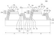
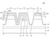
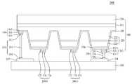
도 7은 또 다른 실시예에 따른 발광 소자 어레이(200E)의 평면도를 나타내고, 도 8은 도 7에 도시된 발광 소자 어레이(200E)의 8-8'선을 따라 절개한 단면도를 나타내고, 도 9는 도 7에 도시된 발광 소자 어레이(200E)의 9-9'선을 따라 절개한 단면도를 나타내고, 도 10은 도 7에 도시된 발광 소자 어레이(200E)의 10-10'선을 따라 절개한 단면도를 나타내고, 도 11은 도 7에 도시된 발광 소자 어레이(200E)의 11-11'선을 따라 절개한 단면도를 나타낸다.7 is a plan view of a light emitting
도 7 내지 도 11을 참조하면, 발광 소자 어레이(200E)는 기판(210), 버퍼층(212), 복수의 발광 영역들(P1 내지 Pn, n>1인 자연수)로 구분되는 발광 구조물(220), 전도층(150a), 제1 절연층(180), 제1 전극층(250), 도전형 상호 연결층(240-1 내지 240-m, m≥1인 자연수), 적어도 하나의 중간 패드(262, 264) 및 제2 전극층(140)을 포함한다.Referring to FIGS. 7 to 11, the light emitting
기판(210), 버퍼층(212) 및 발광 구조물(220)은 도 1의 기판(10), 버퍼층(12) 및 발광 구조물(20)에 각각 해당하므로 이들에 대한 상세한 설명은 생략한다.Since the
하부 반도체층(222)은 n형 반도체층이고, 상부 반도체층(226)은 p형 반도체층으로 구현될 수 있으며, 이에 따라 발광 구조물(220)은 N-P 접합, P-N 접합, N-P-N 접합, 및 P-N-P 접합 구조 중 적어도 하나를 포함할 수 있다.The
발광 구조물(220)은 복수 개의 서로 이격된 발광 영역들(P1 내지 Pn, n>1인 자연수) 및 경계 영역(S)을 포함할 수 있다. 이때 경계 영역(S)은 발광 영역들(P1 내지 Pn, n>1인 자연수) 사이에 위치하는 영역일 수 있다. 또는, 경계 영역(S)은 발광 영역들(P1 내지 Pn, n>1인 자연수) 각각의 둘레에 위치하는 영역일 수 있다. 경계 영역(S)은 발광 구조물(220)을 복수의 발광 영역들(P1 내지 Pn, n>1인 자연수)로 구분하기 위하여 발광 구조물(220)을 메사 식각하여 하부 반도체층(222)의 일부가 노출되는 영역일 수 있다. 복수의 발광 영역들(P1 내지 Pn, n>1인 자연수) 각각의 면적은 동일할 수 있으나, 이에 한정되는 것은 아니다.The
하나의 칩(single chip)의 발광 구조물(220)은 경계 영역(S)에 의하여 복수 개의 발광 영역들(P1 내지 Pn, n>1인 자연수)로 구분될 수 있다.The
전도층(150a)은 상부 반도체층(226) 상에 배치되며, 도 1의 전도층(50a)과 동일하므로, 이에 대한 상세한 설명은 생략한다.The
제1 절연층(180)은 도 3 내지 도 6의 제1 절연층(180)과 동일하며, 전술한 바와 같이 제2 분산 브래그 반사층으로 이루어질 수 있다. 제2 분산 브래그 반사층(180)은 복수의 발광 영역들(P1 내지 Pn, n>1인 자연수) 및 경계 영역(S) 상에 배치된다. 예컨대, 제2 분산 브래그 반사층(180)은 복수의 발광 영역들(P1 내지 Pn, n>1인 자연수)의 상면 및 측면을 덮고, 경계 영역(S)을 덮을 수 있다.The first insulating
제2 분산 브래그 반사층(180)은 복수의 발광 영역들(P1 내지 Pn, n>1인 자연수)로부터 입사되는 빛을 반사시킨다. 따라서 제2 분산 브래그 반사층(180)은 복수의 발광 영역들(P1 내지 Pn, n>1인 자연수)로부터 입사되는 빛이 제2 전극층(140), 도전형 상호 연결층(240-1 내지 240-n, n>1인 자연수) 및 중간 패드(262, 264)에 흡수되는 것을 차단하기 때문에, 실시예는 발광 효율을 향상시킬 수 있다.The second dispersion Bragg
도 7 및 도 8을 참조하면, 제1 전극층(250)은 복수의 발광 영역들(P1 내지 Pn, 예컨대, n=9) 중 다른 어느 하나의 발광 영역(예컨대, P1)의 상부 반도체층(226) 상에 배치된다. 제1 전극층(250)은 상부 반도체층(226) 또는 전도층(150a)과 접촉할 수 있다. 예컨대, 제1 전극층(250)은 직렬 연결되는 발광 영역들 중 첫 번째 발광 영역(예컨대, P1)의 전도층(150a)과 접촉할 수 있다.Referring to FIGS. 7 and 8, the
제1 전극층(250)은 제2 분산 브래그 반사층(180) 상에 배치되는 제1 패드(252) 및 가지 전극(254)을 포함할 수 있다. 제1 패드(252)는 제1 전원을 제공하기 위한 와이어(미도시)가 본딩되고, 가지 전극(254)은 제1 패드(252)로부터 확장되고, 제2 분산 브래그 반사층(180)을 관통하여 전도층(150a)과 접촉하는 적어도 하나의 부분(256)을 가질 수 있다. 여기서, 제1 전극층(250)을 구성하는 제1 접합층(132), 제1 배리어층(136) 및 제1 본딩층(134)은 도 2b에 도시된 제1 접합층(32), 제1 배리어층(36) 및 제1 본딩층(134)과 동일하므로 이에 대한 상세한 설명은 생략한다. 또한, 제1 전극층(250)은 제1 접합층(132)과 제1 본딩층(134)만으로 이루어질 수도 있다.The
도 7 및 도 11을 참조하면, 제2 전극층(140)은 복수의 발광 영역들(P1 내지 Pn, 예컨대, n=9) 중 어느 하나의 발광 영역(예컨대, P9)의 하부 반도체층(222) 상에 배치되며, 하부 반도체층(222)과 접촉할 수 있다. 제2 전극층(140)은 제2 전원을 제공하기 위한 와이어(미도시)가 본딩되는 제2 패드를 포함할 수 있다. 도 7의 실시 예에서는 제2 전극층(140)가 제2 패드 역할을 할 수 있다. 여기서, 제2 접합층(142), 제2 배리어층(146) 및 제2 본딩층(144)은 도 2b에 도시된 제1 접합층(32), 제1 배리어층(36) 및 제1 본딩층(134)과 동일하므로 이에 대한 상세한 설명은 생략한다. 또한, 제2 전극층(140)은 제2 접합층(142)과 제2 본딩층(144)만으로 이루어질 수도 있다.7 and 11, the
도전형 상호 연결층(240-1 내지 240-m, 예컨대, m=8)은 제2 분산 브래그 반사층(180) 상에 배치되며, 복수의 발광 영역들(P1 내지 Pn, 예컨대, n=9)을 전기적으로 직렬 연결한다. 예컨대, 도전형 상호 연결층(240-1 내지 240-m, 예컨대, m=8)은 제1 전극층(250)이 위치하는 제1 발광 영역(P1)을 시점으로 하고, 제2 전극층(140)이 위치하는 제9 발광 영역(P9)을 종점으로 하여 복수의 발광 영역들(P1 내지 P9)을 직렬 연결할 수 있다.The conductive interconnect layers 240-1 to 240-m (eg, m = 8) are disposed on the second dispersion Bragg
도전형 상호 연결층(240-1 내지 240-m)은 제3 접착층(172), 제3 배리어층(176), 제3 본딩층(174)으로 이루어진다. 여기서, 제3 접합층(172), 제3 배리어층(176) 및 제3 본딩층(174)은 도 2b에 도시된 제1 접합층(32), 제1 배리어층(36) 및 제1 본딩층(134)과 동일하므로 이에 대한 상세한 설명은 생략한다. 또한, 도전형 상호 연결층(240-1 내지 240-m)은 제3 접합층(172)과 제3 본딩층(174)만으로 이루어질 수도 있다.The conductive interconnect layers 240-1 to 240-m include a third
각 도전형 상호 연결층(예를 들면 240-1)은 인접하는 발광 영역들(예컨대, P1 및 P2) 중 어느 하나의 발광 영역(P1)의 하부 반도체층(222)과 나머지 다른 하나의 발광 영역(예컨대, P2)의 전도층(150a)을 서로 전기적으로 연결할 수 있다.Each conductive type interconnection layer (for example, 240-1) has a
전도층(150a)이 생략되는 다른 실시 예서는 도전형 상호 연결층(예컨대, 240-1)은 어느 하나의 발광 영역(예컨대, P1)의 하부 반도체층(222)과 나머지 다른 하나의 발광 영역(예컨대, P2)의 상부 반도체층(226)을 전기적으로 연결할 수 있다.In another embodiment in which the
발광 소자 어레이(200E)에 포함되는 서로 직렬 연결되는 복수의 발광 영역들(P1 내지 Pn, n>1인 자연수)을 순서대로 제1 발광 영역 내지 제n 발광 영역이라 한다. 즉 제1 전극층(250)이 위치하는 발광 영역을 제1 발광 영역(P1)이라 하고, 제2 전극층(140)이 위치하는 발광 영역을 제n 발광 영역이라 한다. 여기서 "인접하는 발광 영역들"은 제k 발광 영역과 제k+1 발광 영역일 수 있으며, 제k 도전형 상호 연결층은 제k 발광 영역과 제k+1 발광 영역을 전기적으로 직렬 연결할 수 있고, 1≤k≤(n-1)일 수 있다.The plurality of light-emitting regions (P1 to Pn, a natural number of n> 1) that are serially connected to each other included in the light-emitting
즉, 제k 도전형 상호 연결층은 제k 발광 영역의 하부 반도체층(222)과 제k+1 발광 영역의 상부 반도체층(226) 또는 전도층(150a)을 전기적으로 연결할 수 있다.That is, the k-th conductivity type interconnection layer may electrically connect the
예컨대, 도 8을 참조하면, 제k 도전형 상호 연결층(예컨대, k=2)은 제k 발광 영역(예컨대, k=2), 제k+1 발광 영역(예컨대, k=2) 및 그 사이의 경계 영역(S) 상에 위치할 수 있다. 그리고 제k 도전형 상호 연결층(예컨대, 240-2)은 제2 분산 브래그 반사층(180)을 관통하여 제k+1 발광 영역(예컨대, P3)의 전도층(150a)(또는 상부 반도체층(226))과 접촉하는 적어도 하나의 제1 부분(예컨대, 272)을 가질 수 있다. 도 7에 도시된 실선의 동그라미는 도전형 상호 연결층들(240-1 내지 240-m, 예컨대, m=8)의 제1 부분(272)을 나타낸다.For example, referring to FIG. 8, the k-th conductivity-type interconnect layer (eg, k = 2) includes a k-th emission area (eg, k = 2), a k + 1 emission area (eg, k = 2), and It may be located on the boundary area (S) between. In addition, the k-th conductive interconnect layer (eg, 240-2) penetrates through the second dispersion Bragg
제2 분산 브래그 반사층(180)은 경계 영역(S)에 위치하는 발광 구조물(220)과 도전형 상호 연결층(예컨대, 240-2) 사이에 배치될 수 있다.The second dispersion Bragg
또한, 제k 도전형 상호 연결층(예컨대, 240-2)은 제k 발광 영역(예컨대, P2)의 제2 분산 브래그 반사층(180), 전도층(150a), 상부 반도체층(226) 및 활성층(224)을 관통하여 하부 반도체층(222)과 접촉하는 적어도 하나의 제2 부분(예컨대, 274)을 가질 수 있다. 도 7에 도시된 점선의 동그라미는 도전형 상호 연결층들(240-1 내지 240-m, 예컨대, m=8)의 제2 부분(274)을 나타낸다.In addition, the k-th conductivity type interconnect layer (eg, 240-2) includes a second dispersed Bragg
이때 제2 분산 브래그 반사층(180)은 제k 도전형 상호 연결층(예컨대, 240-2)과 전도층(150a) 사이, 제k 도전형 상호 연결층(예컨대, 240-2)의 제2 부분(274)과 상부 반도체층(226) 사이 및 제k 도전형 상호 연결층(예컨대, 240-2)의 제2 부분(274)과 활성층(224) 사이에 위치하여 서로를 전기적으로 절연시킬 수 있다. 즉, 제2 분산 브래그 반사층(180)은 제k 발광 영역(예컨대, P2)의 전도층(150a), 상부 반도체층(226) 및 활성층(224)으로부터 제k 도전형 상호 연결층(예컨대, 240-2)을 전기적으로 절연시키는 역할을 할 수 있다.At this time, the second dispersion Bragg
도 3 내지 도 6에 예시된 발광 소자 어레이(200A ~ 200D)의 경우, 하부 반도체층(222)과 연결되는 제2 전극층(140)을 형성하기 위해 발광 구조물(220)을 식각하여 하부 반도체층(222)을 노출시키는 메사 식각을 한다. 그리고 일반적으로 메사 식각된 부분만큼 발광 소자의 발광 영역이 감소한다.In the case of the light emitting
그러나, 도 7 내지 도 11에 예시된 발광 소자 어레이에서, 제k 도전형 상호 연결층(예컨대, 240-2)의 제2 부분(예컨대, 274)은 홀(hole) 또는 홈(groove)에 전극 물질이 채워진 형태로 형성될 수 있고 이로 인하여 메사 식각에 의하여 손실되는 발광 영역이 감소하기 때문에, 실시예는 발광 면적을 증대시킬 수 있다.However, in the light emitting device array illustrated in FIGS. 7 to 11, the second portion (eg, 274) of the k-th conductivity type interconnect layer (eg, 240-2) is an electrode in a hole or groove. Since the material may be formed in a filled form, thereby reducing the emission area lost due to the mesa etching, the embodiment may increase the emission area.
도 8을 참조하면, 제k 도전형 상호 연결층(예컨대, 240-2)의 제2 부분(274)의 하면(278)은 활성층(224)의 하면(276)보다 아래에 위치할 수 있다.Referring to FIG. 8, the
도 7, 도 8 및 도 10을 참조하면, 중간 패드(262, 264)는 발광 영역들(P1 내지 Pn, n>1인 자연수) 중 적어도 하나의 발광 영역의 제2 분산 브래그 반사층(180) 상에 배치되며, 상부 반도체층(226) 또는 전도층(150a)과 전기적으로 연결될 수 있다. 중간 패드(262, 264)는 제2 전원을 공급하기 위하여 와이어가 본딩되는 영역일 수 있다.Referring to FIGS. 7, 8 and 10, the
예컨대, 중간 패드(262, 264)는 제1 전극층(250) 및 제2 전극층(140)이 위치하는 발광 영역들(예컨대, P1 및 P9)을 제외한 발광 영역들(예컨대, P2 내지 P8) 중 적어도 하나의 발광 영역(예컨대, P3, P6)의 제2 분산 브래그 반사층(180) 상에 배치될 수 있다.For example, the
중간 패드(262, 264)와 전도층(150a) 사이에 제2 분산 브래그 반사층(180)이 위치하고, 중간 패드(262)는 동일 발광 영역(예컨대, P3) 내에 위치하는 도전형 상호 연결층(예컨대, 240-2)과 연결되고, 중간 패드(264)는 동일 발광 영역(예컨대, P6) 내에 위치하는 도전형 상호 연결층(예컨대, 240-5)과 연결될 수 있다.The second dispersion Bragg
그러나 다른 실시 예에서는 중간 패드의 일부가 제2 분산 브래그 반사층(180)을 관통하여 전도층(150a)과 직접 연결될 수도 있다. 이 경우, 동일 발광 영역 내에 위치하는 중간 패드와 도전형 상호 연결층은 연결될 수도 있고, 연결되지 않을 수도 있다.However, in another embodiment, a portion of the intermediate pad may pass through the second dispersion Bragg
도 12는 도 7에 도시된 발광 소자 어레이(200E)의 회로도를 나타낸다. 도 7 및 도 12를 참조하면, 발광 소자 어레이(200E)는 공통된 하나의 (+) 단자, 예컨대, 하나의 제1 패드(252)를 가지며, 2 이상의 (-) 단자, 예컨대, 제2 패드(140)와 적어도 하나의 중간 패드(262, 264)를 가질 수 있다.12 shows a circuit diagram of the light emitting
따라서, 복수의 (-) 단자인 패드들(140, 262, 264)을 구비함으로써 다양한 구동 전압을 사용할 수 있고, 다양한 밝기의 발광을 구현하도록 조절할 수 있다. 예컨대, 하나의 발광 영역을 구동하는 구동 전압이 3.4V라고 할 때, 발광 소자 어레이(200E)에 인가되는 구동 전압이 6.8V이면, 제1 중간 패드(262)에 제2 전원을 공급하여, 제1 및 제2 발광 영역들(P1, P2)을 구동할 수 있다.Accordingly, by providing a plurality of (-)
또한, 발광 소자 어레이(200E)에 인가되는 구동 전압이 17V이면, 제2 중간 패드(264)에 제2 전원을 공급하여, 제1 내지 제5 발광 영역들(P1 내지 P5)을 구동할 수 있다.In addition, when the driving voltage applied to the light emitting
그리고, 발광 소자 어레이(200E)에 인가되는 구동 전압이 30.6V이면, 제2 패드(140)에 제2 전원을 공급하여, 제1 내지 제9 발광 영역들(P1 내지 P9)을 구동할 수 있다.Then, when the driving voltage applied to the light emitting
이와 같이 실시예는 인가되는 구동 전압에 따라, 중간 패드(262, 264)와 제2 패드(140) 중 어느 하나에 제2 전원을 공급하여, 발광 영역들 중 일부 또는 전부를 구동하도록 설계될 수 있다.As described above, the embodiment may be designed to drive a part or all of the light emitting areas by supplying a second power to any one of the
또한, 구동 전압이 고전압일 경우에, 고전압에 상응하는 개수만큼의 발광 영역들을 배치하면 된다. 예를 들어, 하나의 발광 영역을 구동하는 구동 전압이 4볼트이고, 발광 소자 어레이(200E)에 인가되는 구동 전압이 200V이면, 50개(n=50)만큼의 발광 영역들이 배치되도록 설계하면 된다.In addition, when the driving voltage is a high voltage, it is sufficient to arrange as many light emitting regions as the number corresponding to the high voltage. For example, if the driving voltage driving one light emitting area is 4 volts and the driving voltage applied to the light emitting
또한, 도전형 상호 연결층들(240-1 내지 240-m, m≥인 자연수)이 전도층(150a) 또는 하부 반도체층(222)과 점 접촉(point contact)하기 때문에, 발광 면적을 증대시키고, 전류를 분산시켜 발광 효율을 향상시킬 수 있다.In addition, since the conductive interconnection layers 240-1 to 240-m, a natural number with m≥ is in point contact with the
제2 분산 브래그 반사층(180)에 의하여 제1 전극층(250), 도전형 상호 연결층(240-1 내지 240-n, n>1인 자연수) 및 중간 패드(262, 264)로 빛이 흡수되어 손실되는 것을 차단함으로써, 실시예는 발광 효율을 향상시킬 수 있다.Light is absorbed by the
도 13은 또 다른 실시예에 따른 발광 소자를 포함하는 발광 소자 어레이(200F)의 단면도를 나타낸다.13 is a sectional view of a light emitting
도 13을 참조하면, 발광 소자 어레이(200F)는 서브 마운트(submount, 310), 제1 금속층(332), 제2 금속층(334), 제1 범프부(310), 제2 범프부(320) 및 발광 소자 어레이(340)를 포함한다.Referring to FIG. 13, the light emitting
도 13의 발광 소자 어레이는 도 7에 도시된 발광 소자 어레이(200E)를 플립 칩 형태로 구현한 일 례이지만, 실시예는 이에 한정되는 것은 아니며, 다른 실시 예에 따른 발광 소자 어레이(200A ~ 200D)가 도 13에 도시된 바와 같은 플립 칩 형태로 구현될 수 있다.The light emitting device array of FIG. 13 is an example of implementing the light emitting
서브 마운트(310)는 발광 소자 어레이(340)를 실장한다. 서브 마운트(310)는 패키지 몸체(package body) 또는 인쇄 회로 기판(Printed Circuit Board) 등으로 구현될 수 있으며, 발광 소자 어레이(340)가 플립 칩 본딩(flip chip bonding)될 수 있는 다양한 형태일 수 있다.The sub-mount 310 mounts the light-emitting
발광 소자 어레이(340)는 서브 마운트(310) 상에 배치되고, 제1 범프부(310) 및 제2 범프부(320)에 의하여 서브 마운트(310)와 전기적으로 연결된다. 도 13에 도시된 발광 소자 어레이(340)는 도 11에 도시된 발광 소자 어레이(200E)와 동일한 단면을 갖는다. 따라서, 동일한 부분에 대해서는 설명을 생략한다.The light emitting
서브 마운트(310)는 폴리프탈아미드(PolyPhthal Amide, PPA), 액정 고분자(Liquid Crystal Polymer, LCP), 폴리아미드9T(PolyAmide9T, PA9T), 등과 같은 수지, 금속, 감광성 유리(photo sensitive glass), 사파이어, 세라믹, 인쇄회로기판(Printed Circuit Board) 등을 포함할 수 있다. 그러나 실시 예에 따른 서브 마운트(310)가 이러한 물질로 한정되는 것은 아니다.
제1 금속층(332) 및 제2 금속층(334)은 서브 마운트(310) 상면에 수평 방향으로 서로 이격하여 배치된다. 여기서 서브 마운트(310)의 상면은 발광 소자 어레이(340)에 대향하는 면일 수 있다. 제1 금속층(332) 및 제2 금속층(334)은 전도성 금속, 예컨대, 알루미늄(Al) 또는 로듐(Rh)일 수 있다.The
제1 범프부(310) 및 제2 범프부(320)는 서브 마운트(310)와 발광 소자 어레이(340) 사이에 배치된다. 제1 범프부(310)는 제2 전극층(140)와 제1 금속층(332)을 전기적으로 연결할 수 있다.The
제2 범프부(320)는 제1 전극층(250) 및 중간 패드(262, 264) 중 어느 하나와 제2 금속층(334)을 전기적으로 연결할 수 있다.The
제1 범프부(320)는 제1 확산 방지 접착층(312), 제1 범퍼(bumper, 314) 및 제2 확산 방지 접착층(316)을 포함한다. 제1 범퍼(314)는 제2 전극층(140)와 제1 금속층(332) 사이에 위치한다. 제1 확산 방지 접착층(312)은 제2 전극층(140)과 제1 범퍼(314) 사이에 위치하고, 제1 범퍼(314)와 제2 전극층(140)을 서로 접합시킨다. 즉, 제1 확산 방지 접착층(312)은 제1 범퍼(314)와 제2 전극층(140) 사이의 접착력을 향상시키고, 제1 범퍼(314)에 포함된 이온이 제2 전극층(140)를 통하여 발광 구조물(220)로 침투 또는 확산하는 것을 방지하는 역할을 한다.The
제2 확산 방지 접착층(316)은 제1 범퍼(314)와 제1 금속층(332) 사이에 배치되고, 제1 범퍼(314)와 제1 금속층(332)을 접합시킨다. 제2 확산 방지 접착층(316)은 제1 범퍼(314)와 제1 금속층(332) 사이의 접착력을 향상시키고, 제1 범퍼(314)에 포함된 이온이 제1 금속층(332)을 통하여 서브 마운트(310)로 침투 또는 확산하는 것을 방지하는 역할을 한다.The second diffusion preventing
제2 범프부(320)는 제3 확산 방지 접착층(322), 제2 범퍼(324), 및 제4 확산 방지 접착층(326)을 포함한다. 제2 범퍼(324)는 제1 전극층(250) 및 중간 패드(262, 264) 중 어느 하나와 제2 금속층(334) 사이에 위치한다.The
제3 확산 방지 접착층(322)은 제1 전극층(250) 및 중간 패드(262, 264) 중 어느 하나와 제2 범퍼(324) 사이에 위치하고, 양자를 서로 접합시킨다. 즉 제3 확산 방지 접착층(322)은 접착력을 향상시키고, 제2 범퍼(324)에 포함된 이온이 제1 전극층(250) 또는 중간 패드(262, 264)를 통하여 발광 구조물(220)로 침투 또는 확산하는 것을 방지하는 역할을 한다.The third diffusion preventing
제4 확산 방지 접착층(326)은 제2 범퍼(324)와 제2 금속층(334) 사이에 배치되고, 제2 범퍼(324)와 제2 금속층(334)을 접합시킨다. 제4 확산 방지 접착층(326)은 제2 범퍼(324)와 제2 금속층(334) 사이의 접착력을 향상시키고, 제2 범퍼(324)에 포함된 이온이 제2 금속층(334)을 통하여 서브 마운트(310)로 침투 또는 확산하는 것을 방지하는 역할을 한다.The fourth
제1 내지 제4 확산 방지 접착층(312, 316, 322, 326)은 Pt, Ti, W/Ti, Au 중 적어도 하나 또는 이들의 합금일 수 있다. 또한 제1 범프(314) 및 제2 범프(324)는 티타늄(Ti), 구리(Cu), 니켈(Ni), 금(Au), 크롬(Cr), 탄탈늄(Ta), 백금(Pt), 및 주석(Sn) 중 적어도 하나를 포함할 수 있다.The first to fourth diffusion barrier layers 312, 316, 322, and 326 may be at least one of Pt, Ti, W / Ti, and Au, or alloys thereof. In addition, the
실시예는 제1 전극층(250), 도전형 상호 연결층(240-1 내지 240-n, n>1인 자연수) 및 중간 패드(262, 264)로 빛이 흡수되어 손실되는 것을 제2 분산 브래그 반사층(180)에 의하여 차단함으로써, 발광 효율을 향상시킬 수 있다.In the embodiment, the second dispersion Bragg absorbs and loses light through the
실시예에 따른 발광 소자 패키지는 복수 개가 기판 상에 어레이되며, 발광 소자 패키지의 광 경로 상에 광학 부재인 도광판, 프리즘 시트, 확산 시트 등이 배치될 수 있다. 이러한 발광 소자 패키지, 기판, 광학 부재는 백라이트 유닛으로 기능할 수 있다.A plurality of light emitting device packages according to embodiments are arranged on a substrate, and a light guide plate, a prism sheet, a diffusion sheet, and the like, which are optical members, may be disposed on an optical path of the light emitting device package. The light emitting device package, the substrate, and the optical member may function as a backlight unit.
또 다른 실시 예는 상술한 실시 예들에 기재된 발광 소자 또는 발광 소자 패키지를 포함하는 표시 장치, 지시 장치, 조명 시스템으로 구현될 수 있으며, 예를 들어, 조명 시스템은 램프, 가로등을 포함할 수 있다.Another embodiment may be implemented as a display device, an indication device, and a lighting system including the light emitting device or the light emitting device package described in the above-described embodiments, for example, the lighting system may include a lamp, a street light.
도 14는 실시 예에 따른 발광 소자 패키지를 포함하는 조명 장치의 분해 사시도이다. 도 14를 참조하면, 조명 장치는 광을 투사하는 광원(750)과 광원(750)이 내장되는 하우징(700)과 광원(750)의 열을 방출하는 방열부(740) 및 광원(750)과 방열부(740)를 하우징(700)에 결합하는 홀더(760)를 포함한다.14 is an exploded perspective view of a lighting device including a light emitting device package according to an embodiment. Referring to FIG. 14, the lighting device includes a
하우징(700)은 전기 소켓(미도시)에 결합되는 소켓 결합부(710)와, 소켓 결합부(710)와 연결되고 광원(750)이 내장되는 몸체부(730)를 포함한다. 몸체부(730)에는 하나의 공기 유동구(720)가 관통하여 형성될 수 있다.The
하우징(700)의 몸체부(730) 상에 복수 개의 공기 유동구(720)가 구비되며, 공기 유동구(720)는 하나이거나, 복수 개일 수 있다. 공기 유동구(720)는 몸체부(730)에 방사상으로 배치되거나 다양한 형태로 배치될 수 있다.A plurality of
광원(750)은 기판(754) 상에 구비되는 복수 개의 발광 소자 패키지(752)를 포함한다. 기판(754)은 하우징(700)의 개구부에 삽입될 수 있는 형상일 수 있으며, 후술하는 바와 같이 방열부(740)로 열을 전달하기 위하여 열전도율이 높은 물질로 이루어질 수 있다. 복수 개의 발광 소자 패키지는 상술한 실시 예일 수 있다.The
광원(750)의 하부에는 홀더(760)가 구비되며, 홀더(760)는 프레임 및 다른 공기 유동구를 포함할 수 있다. 또한, 도시되지는 않았으나 광원(750)의 하부에는 광학 부재가 구비되어 광원(750)의 발광 소자 패키지(752)에서 투사되는 빛을 확산, 산란 또는 수렴시킬 수 있다.A
도 15는 실시 예에 따른 발광 소자 패키지를 포함하는 표시 장치를 나타낸다.15 illustrates a display device including a light emitting device package according to an embodiment.
도 15를 참조하면, 표시 장치(800)는 바텀 커버(810)와, 바텀 커버(810) 상에 배치되는 반사판(820)과, 광을 방출하는 발광 모듈(830, 835)과, 반사판(820)의 전방에 배치되며 상기 발광 모듈(830, 835)에서 발산되는 빛을 표시 장치 전방으로 안내하는 도광판(840)과, 도광판(840)의 전방에 배치되는 프리즘 시트들(850, 860)을 포함하는 광학 시트와, 광학 시트 전방에 배치되는 디스플레이 패널(870)과, 디스플레이 패널(870)과 연결되고 디스플레이 패널(870)에 화상 신호를 공급하는 화상 신호 출력 회로(872)와, 디스플레이 패널(870)의 전방에 배치되는 컬러 필터(880)를 포함할 수 있다. 여기서 바텀 커버(810), 반사판(820), 발광 모듈(830, 835), 도광판(840), 및 광학 시트는 백라이트 유닛(Backlight Unit)을 이룰 수 있다.Referring to FIG. 15, the
발광 모듈은 기판(830) 상의 발광 소자 패키지(835)를 포함하여 이루어진다. 여기서, 기판(830)은 PCB 등이 사용될 수 있다. 발광 소자 패키지(835)는 실시 예에 따른 발광 소자 패키지일 수 있다.The light emitting module includes a light emitting
바텀 커버(810)는 표시 장치(800) 내의 구성 요소들을 수납할 수 있다. 그리고, 반사판(820)은 본 도면처럼 별도의 구성요소로 마련될 수도 있으며, 도광판(840)의 후면이나, 바텀 커버(810)의 전면에 반사도가 높은 물질로 코팅되는 형태로 마련되는 것도 가능하다.The
여기서, 반사판(820)은 반사율이 높고 초박형으로 사용 가능한 소재를 사용할 수 있고, 폴리에틸렌 테레프탈레이트(PolyEthylene Terephtalate; PET)를 사용할 수 있다.Here, the
그리고, 도광판(830)은 폴리메틸메타크릴레이트(PolyMethylMethAcrylate; PMMA), 폴리카보네이트(PolyCarbonate; PC), 또는 폴리에틸렌(PolyEthylene; PE) 등으로 형성될 수 있다.In addition, the
그리고, 제1 프리즘 시트(850)는 지지 필름의 일면에, 투광성이면서 탄성을 갖는 중합체 재료로 형성될 수 있으며, 중합체는 복수 개의 입체구조가 반복적으로 형성된 프리즘층을 가질 수 있다. 여기서, 복수 개의 패턴은 도시된 바와 같이 마루와 골이 반복적으로 스트라이프 타입으로 구비될 수 있다.In addition, the
그리고, 제2 프리즘 시트(860)에서 지지 필름 일면의 마루와 골의 방향은, 제1 프리즘 시트(850) 내의 지지필름 일면의 마루와 골의 방향과 수직할 수 있다. 이는 발광 모듈과 반사 시트로부터 전달된 빛을 디스플레이 패널(1870)의 전면으로 고르게 분산하기 위함이다.In addition, in the
그리고, 도시되지는 않았으나, 도광판(840)과 제1 프리즘 시트(850) 사이에 확산 시트가 배치될 수 있다. 확산 시트는 폴리에스터와 폴리카보네이트 계열의 재료로 이루어질 수 있으며, 백라이트 유닛으로부터 입사된 빛을 굴절과 산란을 통하여 광 투사각을 최대로 넓힐 수 있다. 그리고, 확산 시트는 광확산제를 포함하는 지지층과, 광출사면(제1 프리즘 시트 방향)과 광입사면(반사시트 방향)에 형성되며 광확산제를 포함하지 않는 제1 레이어와 제2 레이어를 포함할 수 있다.In addition, although not illustrated, a diffusion sheet may be disposed between the
실시 예에서 확산 시트, 제1 프리즘시트(850), 및 제2 프리즘시트(860)가 광학 시트를 이루는데, 광학 시트는 다른 조합 예를 들어, 마이크로 렌즈 어레이로 이루어지거나 확산 시트와 마이크로 렌즈 어레이의 조합 또는 하나의 프리즘 시트와 마이크로 렌즈 어레이의 조합 등으로 이루어질 수 있다.In an embodiment, the diffusion sheet, the
디스플레이 패널(870)은 액정 표시 패널(Liquid crystal display)가 배치될 수 있는데, 액정 표시 패널 외에 광원을 필요로 하는 다른 종류의 표시 장치가 구비될 수 있다.The
이상에서 실시예를 중심으로 설명하였으나 이는 단지 예시일 뿐 본 발명을 한정하는 것이 아니며, 본 발명이 속하는 분야의 통상의 지식을 가진 자라면 본 실시예의 본질적인 특성을 벗어나지 않는 범위에서 이상에 예시되지 않은 여러 가지의 변형과 응용이 가능함을 알 수 있을 것이다. 예를 들어, 실시예에 구체적으로 나타난 각 구성 요소는 변형하여 실시할 수 있는 것이다. 그리고 이러한 변형과 응용에 관계된 차이점들은 첨부된 청구 범위에서 규정하는 본 발명의 범위에 포함되는 것으로 해석되어야 할 것이다.The embodiments have been mainly described above, but this is merely an example and does not limit the present invention, and those of ordinary skill in the art to which the present invention pertains are not exemplified above in the range that does not depart from the essential characteristics of the present embodiment. It will be appreciated that various modifications and applications are possible. For example, each component specifically shown in the embodiments can be implemented by modification. And differences related to these modifications and applications should be construed as being included in the scope of the invention defined in the appended claims.
10, 210: 기판12, 212 : 버퍼층
20, 220, 220a, 220b: 발광 구조물
22, 222, 222a, 222b: 제1 도전형 반도체층
24, 224, 224a, 224b: 활성층
26, 226, 226a, 226b: 제2 도전형 반도체층
30, 130a, 130b, 250: 제1 전극층32, 132a, 132b: 제1 접착층
34, 134a, 134b: 제1 본딩층36, 136a, 136b: 제1 배리어층
40, 140a, 140b: 제2 전극층42, 142a, 142b: 제2 접착층
44, 144a, 144b: 제2 본딩층46, 146a, 146b: 제2 배리어층
50a, 50b, 150a, 150b: 도전층60, 160a, 160b: 전류 차단층
100: 발광 소자200A ~ 200F, 340: 발광 소자 어레이
170, 240-1 ~ 240-8: 도전형 상호 연결층
180, 182: 절연층262, 264: 중간 패드
310: 서브 마운트332, 334: 금속층
310: 320: 범프부700: 하우징
740: 방열부750: 광원
760: 홀더800: 표시 장치
810: 바텀 커버820: 반사판
830, 835: 발광 모듈840: 도광판
850, 860: 프리즘 시트10, 210:
20, 220, 220a, 220b: light emitting structure
22, 222, 222a, 222b: first conductivity type semiconductor layer
24, 224, 224a, 224b: active layer
26, 226, 226a, 226b: second conductivity type semiconductor layer
30, 130a, 130b, 250:
34, 134a, 134b:
40, 140a, 140b:
44, 144a, 144b:
50a, 50b, 150a, 150b:
100: light-emitting
170, 240-1 ~ 240-8: conductive interconnect layer
180, 182: insulating
310: sub-mount 332, 334: metal layer
310: 320: bump portion 700: housing
740: heat dissipation unit 750: light source
760: holder 800: display device
810: bottom cover 820: reflector
830, 835: light emitting module 840: light guide plate
850, 860: Prism sheet
Claims (31)
Translated fromKorean상기 기판 위에 배치된 서로 다른 도전형의 하부 및 상부 반도체층, 상기 하부 및 상부 반도체층 사이에 배치된 활성층을 갖는 발광 구조물;
상기 상부 반도체층 위에 배치된 제1 전극층;
상기 하부 도전형 반도체층 위에 배치된 제2 전극층; 및
상기 제1 전극층과 상기 상부 반도체층 사이에 배치된 전류 차단층을 포함하고,
상기 제1 전극층은 서로 중첩된 제1 접착층과 제1 본딩층을 포함하고, 상기 제1 본딩층은 상기 제1 접착층 위에 배치되며, 상기 제1 접착층과 상기 제1 본딩층 사이에 알루미늄(Al)으로 이루어진 반사층이 개재되지 않고,
상기 제2 전극층은 서로 중첩된 제2 접착층과 제2 본딩층을 포함하고, 상기 제2 본딩층은 상기 제2 접착층 위에 배치되며, 상기 제2 접착층과 상기 제2 본딩층 사이에 알루미늄(Al)으로 이루어진 반사층이 개재되지 않고,
상기 제1 접착층은 상기 전류 차단층의 상부와 측부를 직접 접하면서 감싸도록 배치된 발광 소자.Board;
A light emitting structure having lower and upper semiconductor layers of different conductivity types disposed on the substrate, and active layers disposed between the lower and upper semiconductor layers;
A first electrode layer disposed on the upper semiconductor layer;
A second electrode layer disposed on the lower conductivity type semiconductor layer; And
And a current blocking layer disposed between the first electrode layer and the upper semiconductor layer,
The first electrode layer includes a first adhesive layer and a first bonding layer overlapping each other, and the first bonding layer is disposed on the first adhesive layer, and aluminum (Al) is disposed between the first adhesive layer and the first bonding layer. The reflective layer made of is not interposed,
The second electrode layer includes a second adhesive layer and a second bonding layer overlapping each other, and the second bonding layer is disposed on the second adhesive layer, and aluminum (Al) is disposed between the second adhesive layer and the second bonding layer. The reflective layer made of is not interposed,
The first adhesive layer is a light emitting device that is arranged to wrap while directly contacting the top and side of the current blocking layer.
상기 제1 또는 제2 배리어층은 Ni, Cr, Ti 및 Pt 중 적어도 하나를 포함하고,
상기 제1 또는 제2 접착층의 두께는 5 ㎚ 내지 15 ㎚인 발광 소자.According to claim 1, The first or second adhesive layer includes at least one of Cr, Rd and Ti,
The first or second barrier layer includes at least one of Ni, Cr, Ti and Pt,
The first or second adhesive layer has a thickness of 5 nm to 15 nm.
상기 전류 차단층은 분산 브래그 반사층이고,
상기 하부 반도체층의 측면은 경사진 발광 소자.According to claim 1,
The current blocking layer is a distributed Bragg reflective layer,
A side surface of the lower semiconductor layer is an inclined light emitting device.
상기 분산 브래그 반사층은 굴절율이 서로 다른 제1 및 제2 층이 교대로 적어도 2회 이상 적층된 절연 물질을 포함하고,
상기 제1 전극층은 5 ㎛ 내지 100 ㎛의 폭을 갖는 발광 소자.The method of claim 9,
The dispersion Bragg reflective layer includes an insulating material in which the first and second layers having different refractive indices are alternately stacked at least twice or more,
The first electrode layer is a light emitting device having a width of 5 ㎛ to 100 ㎛.
상기 기판 상에 수평 방향으로 서로 이격되어 배열된 복수의 발광 소자;
상기 복수의 발광 소자에서, 2개의 발광 소자를 연결하는 도전형 상호 연결층; 및
상기 복수의 발광 소자와 상기 도전형 상호 연결층 사이에 배치된 제1 절연층을 포함하고,
상기 복수의 발광 소자 각각은
서로 다른 도전형의 하부 및 상부 반도체층, 상기 하부 및 상부 반도체층 사이에 배치된 활성층을 갖는 발광 구조물;
상기 상부 반도체층 위에 배치된 제1 전극층;상기 하부 반도체층 위에 배치된 제2 전극층; 및
상기 제1 전극층과 상기 상부 반도체층 사이에 배치된 전류 차단층을 포함하고,
상기 도전형 상호 연결층은 상기 2개의 발광 소자 중 하나의 상기 제1 전극층과 상기 2개의 발광 소자 중 다른 하나의 제2 전극층을 연결하고,
상기 제1 전극층은 서로 중첩된 제1 접착층과 제1 본딩층을 포함하고, 상기 제1 본딩층은 상기 제1 접착층 위에 배치되며, 상기 제1 접착층과 상기 제1 본딩층 사이에 알루미늄(Al)으로 이루어진 반사층이 개재되지 않고,
상기 도전형 상호 연결층은 서로 중첩된 제3 접착층과 제3 본딩층을 포함하고, 상기 제3 본딩층은 상기 제3 접착층 위에 배치되며, 상기 제3 접착층과 상기 제3 본딩층 사이에 알루미늄(Al)으로 이루어진 반사층이 개재되지 않고,
상기 제1 접착층은 상기 전류 차단층의 상부와 측부를 직접 접하면서 감싸도록 배치된 발광 소자 어레이.Board;
A plurality of light emitting elements arranged on the substrate spaced apart from each other in a horizontal direction;
In the plurality of light emitting elements, a conductive interconnect layer connecting two light emitting elements; And
And a first insulating layer disposed between the plurality of light emitting elements and the conductive interconnect layer,
Each of the plurality of light emitting elements
A light emitting structure having lower and upper semiconductor layers of different conductivity types, and active layers disposed between the lower and upper semiconductor layers;
A first electrode layer disposed on the upper semiconductor layer; a second electrode layer disposed on the lower semiconductor layer; And
And a current blocking layer disposed between the first electrode layer and the upper semiconductor layer,
The conductive interconnect layer connects the first electrode layer of one of the two light emitting elements and the second electrode layer of the other of the two light emitting elements,
The first electrode layer includes a first adhesive layer and a first bonding layer overlapping each other, and the first bonding layer is disposed on the first adhesive layer, and aluminum (Al) is disposed between the first adhesive layer and the first bonding layer. The reflective layer made of is not interposed,
The conductive interconnect layer includes a third adhesive layer and a third bonding layer overlapping each other, and the third bonding layer is disposed on the third adhesive layer, and aluminum (a) is formed between the third adhesive layer and the third bonding layer. Al) is not interposed a reflective layer,
The first adhesive layer is a light emitting device array arranged to wrap while directly contacting the top and side of the current blocking layer.
상기 제2 전극층은 서로 중첩된 상기 제2 접착층과 상기 제2 본딩층을 포함하고, 상기 제2 접착층과 상기 제2 본딩층 사이에 알루미늄(Al)으로 이루어진 반사층이 개재되지 않는 발광 소자 어레이.The method of claim 15, wherein the first electrode layer comprises a first barrier layer disposed in contact with the first adhesive layer, the second bonding layer is disposed on the second adhesive layer,
The second electrode layer includes the second adhesive layer and the second bonding layer overlapping each other, and a light emitting device array in which a reflective layer made of aluminum (Al) is not interposed between the second adhesive layer and the second bonding layer.
상기 도전형 상호 연결층은 상기 제3 접착층 위에 접하여 배치된 제3 배리어층을 포함하는 발광 소자 어레이.The method of claim 16, wherein the second electrode layer comprises a second barrier layer disposed in contact with the second adhesive layer,
The conductive interconnect layer comprises a third barrier layer disposed in contact with the third adhesive layer.
상기 제1, 제2 또는 제3 접착층은 Cr, Rd 및 Ti 중 적어도 하나를 포함하고,
상기 제1, 제2 또는 제3 접착층의 두께는 5 ㎚ 내지 15 ㎚이고,
상기 제1, 제2 또는 제3 배리어층은 Ni, Ti, Cr 및 Pt 중 적어도 하나를 포함하는 발광 소자 어레이.The method of claim 18,
The first, second or third adhesive layer includes at least one of Cr, Rd and Ti,
The thickness of the first, second or third adhesive layer is 5 nm to 15 nm,
The first, second, or third barrier layer includes at least one of Ni, Ti, Cr, and Pt.
상기 제1 및 제2 절연층 중 적어도 하나는 분산 브래그 반사층이고,
상기 도전형 상호 연결층에 의해 연결된 상기 2개의 발광 소자의 제1 및 제2 전극층 및 상기 도전형 상호 연결층은 일체이고,
상기 도전형 상호 연결층의 두께는 상기 제1 전극층의 두께보다 더 두꺼운 발광 소자 어레이.The method of claim 15, further comprising a second insulating layer disposed between the first insulating layer and the plurality of light emitting elements,
At least one of the first and second insulating layers is a dispersion Bragg reflective layer,
The first and second electrode layers of the two light emitting elements connected by the conductive interconnect layer and the conductive interconnect layer are integral,
The thickness of the conductive interconnect layer is a light emitting device array thicker than the thickness of the first electrode layer.
상기 복수의 발광 소자는 상기 도전형 상호 연결층에 의해 서로 직렬 연결된 발광 소자 어레이.16. The method of claim 15, The current blocking layer is a distributed Bragg reflective layer,
The plurality of light emitting devices are light emitting device arrays connected in series with each other by the conductive interconnect layer.
Priority Applications (6)
| Application Number | Priority Date | Filing Date | Title |
|---|---|---|---|
| KR1020120124381AKR102087933B1 (en) | 2012-11-05 | 2012-11-05 | Light Emitting device and light emitting array |
| US14/062,131US9236526B2 (en) | 2012-11-05 | 2013-10-24 | Light emitting device and light emitting device array |
| CN201310534465.0ACN103811597B (en) | 2012-11-05 | 2013-11-01 | Luminescent device and light-emitting element array |
| EP13191337.8AEP2728632B1 (en) | 2012-11-05 | 2013-11-04 | Light emitting device |
| JP2013229122AJP2014093532A (en) | 2012-11-05 | 2013-11-05 | Light-emitting element |
| US14/962,083US9640583B2 (en) | 2012-11-05 | 2015-12-08 | Light emitting device and light emitting device array |
Applications Claiming Priority (1)
| Application Number | Priority Date | Filing Date | Title |
|---|---|---|---|
| KR1020120124381AKR102087933B1 (en) | 2012-11-05 | 2012-11-05 | Light Emitting device and light emitting array |
Publications (2)
| Publication Number | Publication Date |
|---|---|
| KR20140057968A KR20140057968A (en) | 2014-05-14 |
| KR102087933B1true KR102087933B1 (en) | 2020-04-14 |
Family
ID=49513856
Family Applications (1)
| Application Number | Title | Priority Date | Filing Date |
|---|---|---|---|
| KR1020120124381AActiveKR102087933B1 (en) | 2012-11-05 | 2012-11-05 | Light Emitting device and light emitting array |
Country Status (5)
| Country | Link |
|---|---|
| US (2) | US9236526B2 (en) |
| EP (1) | EP2728632B1 (en) |
| JP (1) | JP2014093532A (en) |
| KR (1) | KR102087933B1 (en) |
| CN (1) | CN103811597B (en) |
Families Citing this family (41)
| Publication number | Priority date | Publication date | Assignee | Title |
|---|---|---|---|---|
| US7067849B2 (en) | 2001-07-17 | 2006-06-27 | Lg Electronics Inc. | Diode having high brightness and method thereof |
| US6949395B2 (en)* | 2001-10-22 | 2005-09-27 | Oriol, Inc. | Method of making diode having reflective layer |
| US7148520B2 (en) | 2001-10-26 | 2006-12-12 | Lg Electronics Inc. | Diode having vertical structure and method of manufacturing the same |
| TWI440210B (en) | 2007-01-22 | 2014-06-01 | Cree Inc | Illumination device using external interconnection array of light-emitting device and manufacturing method thereof |
| US9490409B2 (en)* | 2011-10-24 | 2016-11-08 | Formosa Epitaxy Incorporation | Light emmiting diode chip |
| US11792898B2 (en) | 2012-07-01 | 2023-10-17 | Ideal Industries Lighting Llc | Enhanced fixtures for area lighting |
| US11160148B2 (en) | 2017-06-13 | 2021-10-26 | Ideal Industries Lighting Llc | Adaptive area lamp |
| TWI527263B (en)* | 2013-07-17 | 2016-03-21 | 新世紀光電股份有限公司 | Light-emitting diode structure |
| US9502614B2 (en)* | 2014-06-04 | 2016-11-22 | Formosa Epitaxy Incorporation | Light emitting diode chip, light emitting device, and wafer-level structure of light emitting diode |
| JP6269362B2 (en)* | 2014-07-15 | 2018-01-31 | 豊田合成株式会社 | Group III nitride semiconductor light emitting device and method for manufacturing the same |
| KR101888608B1 (en) | 2014-10-17 | 2018-09-20 | 엘지이노텍 주식회사 | Light emitting device package and lighting apparatus |
| DE102014115740A1 (en)* | 2014-10-29 | 2016-05-04 | Osram Opto Semiconductors Gmbh | Optoelectronic semiconductor chip |
| JP6327564B2 (en)* | 2014-11-12 | 2018-05-23 | パナソニックIpマネジメント株式会社 | Semiconductor device |
| KR102322841B1 (en)* | 2014-12-24 | 2021-11-08 | 엘지이노텍 주식회사 | Light emittng device and light emitting device array including the same |
| KR102256632B1 (en)* | 2015-01-21 | 2021-05-26 | 엘지이노텍 주식회사 | Light emitting device and e-beam evaporating apparatus manufacturing the same |
| CN105870280B (en)* | 2015-01-21 | 2019-07-09 | 展晶科技(深圳)有限公司 | LED crystal particle |
| CN110504342A (en)* | 2015-04-22 | 2019-11-26 | 新世纪光电股份有限公司 | Light-emitting element and method of manufacturing the same |
| US10147849B2 (en)* | 2015-05-05 | 2018-12-04 | Xiangneng Hualei Optoelectronic Co., Ltd | Manufacturing method of flip-chip structure of group III semiconductor light emitting device |
| KR102641239B1 (en)* | 2015-07-10 | 2024-02-29 | 서울바이오시스 주식회사 | Light emitting diode, method of fabricating the same, and light emitting device module having the same |
| JP6651843B2 (en) | 2015-12-25 | 2020-02-19 | 日亜化学工業株式会社 | Light emitting element |
| CN109417082B (en)* | 2016-03-18 | 2023-08-01 | Lg伊诺特有限公司 | Semiconductor device and display apparatus including the same |
| US10529696B2 (en) | 2016-04-12 | 2020-01-07 | Cree, Inc. | High density pixelated LED and devices and methods thereof |
| WO2017213455A1 (en)* | 2016-06-10 | 2017-12-14 | 엘지이노텍 주식회사 | Semiconductor device |
| US10964862B2 (en)* | 2016-09-30 | 2021-03-30 | Sensor Electronic Technology, Inc. | Semiconductor heterostructure with multiple active regions |
| JP7290001B2 (en) | 2017-08-03 | 2023-06-13 | クリーエルイーディー・インコーポレーテッド | High-density pixelated LED chips, chip array devices, and methods of making same |
| US10734363B2 (en) | 2017-08-03 | 2020-08-04 | Cree, Inc. | High density pixelated-LED chips and chip array devices |
| KR102370621B1 (en)* | 2017-08-24 | 2022-03-04 | 삼성전자주식회사 | Light emitting package and light emitting module including the same |
| CN111108613B (en) | 2017-09-13 | 2024-01-16 | 夏普株式会社 | LED unit, image display element and manufacturing method thereof |
| US10529773B2 (en) | 2018-02-14 | 2020-01-07 | Cree, Inc. | Solid state lighting devices with opposing emission directions |
| JP6822429B2 (en)* | 2018-02-19 | 2021-01-27 | 日亜化学工業株式会社 | Light emitting element |
| CN108447955B (en)* | 2018-03-16 | 2019-07-23 | 厦门市三安光电科技有限公司 | LED chip construction and preparation method thereof |
| JP7206628B2 (en)* | 2018-04-27 | 2023-01-18 | セイコーエプソン株式会社 | Light-emitting device and projector |
| US10903265B2 (en) | 2018-12-21 | 2021-01-26 | Cree, Inc. | Pixelated-LED chips and chip array devices, and fabrication methods |
| CN109713103B (en)* | 2018-12-28 | 2021-03-02 | 映瑞光电科技(上海)有限公司 | LED chip |
| CN110429166B (en)* | 2019-08-23 | 2020-12-04 | 厦门乾照光电股份有限公司 | an LED chip |
| WO2021087109A1 (en) | 2019-10-29 | 2021-05-06 | Cree, Inc. | Texturing for high density pixelated-led chips |
| US11145789B2 (en) | 2019-11-04 | 2021-10-12 | Epistar Corporation | Light-emitting device |
| KR102742687B1 (en) | 2019-12-03 | 2024-12-16 | 삼성전자주식회사 | Semiconductor light emmiting device |
| US12027501B2 (en)* | 2020-04-02 | 2024-07-02 | Nichia Corporation | Surface light source and method of manufacturing surface light source |
| US11437548B2 (en) | 2020-10-23 | 2022-09-06 | Creeled, Inc. | Pixelated-LED chips with inter-pixel underfill materials, and fabrication methods |
| US20230395732A1 (en)* | 2022-06-01 | 2023-12-07 | Tamura Corporation | Schottky barrier diode |
Citations (3)
| Publication number | Priority date | Publication date | Assignee | Title |
|---|---|---|---|---|
| JP2005079152A (en) | 2003-08-28 | 2005-03-24 | Toshiba Corp | Semiconductor light emitting device and manufacturing method thereof |
| JP2008192710A (en) | 2007-02-01 | 2008-08-21 | Nichia Chem Ind Ltd | Semiconductor light emitting device |
| JP2011243977A (en)* | 2010-05-18 | 2011-12-01 | Seoul Semiconductor Co Ltd | Light emitting diode chip having wavelength converting layer and method of fabricating the same, and package having the light emitting diode chip and method of fabricating the same |
Family Cites Families (27)
| Publication number | Priority date | Publication date | Assignee | Title |
|---|---|---|---|---|
| JPH0936431A (en)* | 1995-07-13 | 1997-02-07 | Toshiba Corp | Semiconductor light emitting device |
| JPH10294531A (en)* | 1997-02-21 | 1998-11-04 | Toshiba Corp | Nitride compound semiconductor light emitting device |
| JPH114020A (en)* | 1997-04-15 | 1999-01-06 | Toshiba Corp | Semiconductor light emitting element, method of manufacturing the same, and semiconductor light emitting device |
| JP2002164575A (en)* | 2000-11-27 | 2002-06-07 | Nichia Chem Ind Ltd | Nitride semiconductor light emitting device |
| US6864571B2 (en)* | 2003-07-07 | 2005-03-08 | Gelcore Llc | Electronic devices and methods for making same using nanotube regions to assist in thermal heat-sinking |
| JP3802910B2 (en)* | 2004-09-13 | 2006-08-02 | ローム株式会社 | Semiconductor light emitting device |
| US8476648B2 (en) | 2005-06-22 | 2013-07-02 | Seoul Opto Device Co., Ltd. | Light emitting device and method of manufacturing the same |
| JP2007281037A (en)* | 2006-04-03 | 2007-10-25 | Dowa Holdings Co Ltd | Semiconductor light emitting element, and its manufacturing method |
| JP4929924B2 (en) | 2006-08-25 | 2012-05-09 | サンケン電気株式会社 | Semiconductor light emitting device, manufacturing method thereof, and composite semiconductor device |
| CN102779918B (en) | 2007-02-01 | 2015-09-02 | 日亚化学工业株式会社 | Semiconductor light-emitting elements |
| US8085825B2 (en)* | 2007-03-06 | 2011-12-27 | Sanyo Electric Co., Ltd. | Method of fabricating semiconductor laser diode apparatus and semiconductor laser diode apparatus |
| US8299501B2 (en)* | 2007-05-30 | 2012-10-30 | Nichia Corporation | Nitride semiconductor device |
| JP5123269B2 (en)* | 2008-09-30 | 2013-01-23 | ソウル オプト デバイス カンパニー リミテッド | Light emitting device and manufacturing method thereof |
| JP5196160B2 (en)* | 2008-10-17 | 2013-05-15 | 日亜化学工業株式会社 | Semiconductor light emitting device |
| WO2010071113A1 (en)* | 2008-12-15 | 2010-06-24 | 昭和電工株式会社 | Semiconductor light emission element |
| JP2010238802A (en)* | 2009-03-30 | 2010-10-21 | Showa Denko Kk | Semiconductor light-emitting element, electrode structure, method for manufacturing semiconductor light-emitting element, and method for manufacturing electrode structure |
| TWI429107B (en)* | 2009-05-14 | 2014-03-01 | Toyoda Gosei Kk | Semiconductor light-emitting element, method of manufacturing the same, lamp, lighting device, electronic device, and mechanical device |
| KR101072034B1 (en)* | 2009-10-15 | 2011-10-10 | 엘지이노텍 주식회사 | Semiconductor light emitting device and fabrication method thereof |
| EP2367203A1 (en)* | 2010-02-26 | 2011-09-21 | Samsung LED Co., Ltd. | Semiconductor light emitting device having multi-cell array and method for manufacturing the same |
| JP2012028749A (en)* | 2010-07-22 | 2012-02-09 | Seoul Opto Devices Co Ltd | Light-emitting diode |
| KR101746004B1 (en)* | 2010-10-29 | 2017-06-27 | 엘지이노텍 주식회사 | Light emitting device |
| KR20120053571A (en)* | 2010-11-18 | 2012-05-29 | 서울옵토디바이스주식회사 | Light emitting diode chip having plurality of mesa structures |
| JP2014500624A (en)* | 2010-11-18 | 2014-01-09 | ソウル バイオシス カンパニー リミテッド | Light emitting diode chip with electrode pad |
| JP2012151441A (en)* | 2010-12-28 | 2012-08-09 | Ricoh Co Ltd | Optical device, optical scanner, and image formation apparatus |
| TWM409542U (en) | 2011-02-01 | 2011-08-11 | Epistar Corp | A light-emitting device |
| JP2012227383A (en)* | 2011-04-20 | 2012-11-15 | Showa Denko Kk | Semiconductor light-emitting element, electrode structure, and light-emitting device |
| TWI555226B (en)* | 2011-07-12 | 2016-10-21 | 晶元光電股份有限公司 | Light-emitting element with multilayer light-emitting laminate |
- 2012
- 2012-11-05KRKR1020120124381Apatent/KR102087933B1/enactiveActive
- 2013
- 2013-10-24USUS14/062,131patent/US9236526B2/enactiveActive
- 2013-11-01CNCN201310534465.0Apatent/CN103811597B/enactiveActive
- 2013-11-04EPEP13191337.8Apatent/EP2728632B1/enactiveActive
- 2013-11-05JPJP2013229122Apatent/JP2014093532A/enactivePending
- 2015
- 2015-12-08USUS14/962,083patent/US9640583B2/enactiveActive
Patent Citations (3)
| Publication number | Priority date | Publication date | Assignee | Title |
|---|---|---|---|---|
| JP2005079152A (en) | 2003-08-28 | 2005-03-24 | Toshiba Corp | Semiconductor light emitting device and manufacturing method thereof |
| JP2008192710A (en) | 2007-02-01 | 2008-08-21 | Nichia Chem Ind Ltd | Semiconductor light emitting device |
| JP2011243977A (en)* | 2010-05-18 | 2011-12-01 | Seoul Semiconductor Co Ltd | Light emitting diode chip having wavelength converting layer and method of fabricating the same, and package having the light emitting diode chip and method of fabricating the same |
Also Published As
| Publication number | Publication date |
|---|---|
| EP2728632A3 (en) | 2014-07-09 |
| US9640583B2 (en) | 2017-05-02 |
| CN103811597B (en) | 2018-12-21 |
| US9236526B2 (en) | 2016-01-12 |
| US20160093667A1 (en) | 2016-03-31 |
| JP2014093532A (en) | 2014-05-19 |
| KR20140057968A (en) | 2014-05-14 |
| CN103811597A (en) | 2014-05-21 |
| EP2728632A2 (en) | 2014-05-07 |
| US20140124730A1 (en) | 2014-05-08 |
| EP2728632B1 (en) | 2021-12-15 |
Similar Documents
| Publication | Publication Date | Title |
|---|---|---|
| KR102087933B1 (en) | Light Emitting device and light emitting array | |
| KR101888604B1 (en) | Light emitting device and light emitting device package | |
| US9735199B2 (en) | Light emitting device | |
| US9620682B2 (en) | Light emitting device | |
| KR101871372B1 (en) | Light emitting device | |
| KR102197082B1 (en) | Light emitting device and light emitting device package including the same | |
| US20140183573A1 (en) | Light emitting device | |
| KR20120136814A (en) | A light emitting device package | |
| KR102087937B1 (en) | Light emitting device |
Legal Events
| Date | Code | Title | Description |
|---|---|---|---|
| PA0109 | Patent application | Patent event code:PA01091R01D Comment text:Patent Application Patent event date:20121105 | |
| PG1501 | Laying open of application | ||
| A201 | Request for examination | ||
| PA0201 | Request for examination | Patent event code:PA02012R01D Patent event date:20171024 Comment text:Request for Examination of Application Patent event code:PA02011R01I Patent event date:20121105 Comment text:Patent Application | |
| E902 | Notification of reason for refusal | ||
| PE0902 | Notice of grounds for rejection | Comment text:Notification of reason for refusal Patent event date:20180828 Patent event code:PE09021S01D | |
| E90F | Notification of reason for final refusal | ||
| PE0902 | Notice of grounds for rejection | Comment text:Final Notice of Reason for Refusal Patent event date:20190225 Patent event code:PE09021S02D | |
| E902 | Notification of reason for refusal | ||
| PE0902 | Notice of grounds for rejection | Comment text:Notification of reason for refusal Patent event date:20191028 Patent event code:PE09021S01D | |
| E701 | Decision to grant or registration of patent right | ||
| PE0701 | Decision of registration | Patent event code:PE07011S01D Comment text:Decision to Grant Registration Patent event date:20200123 | |
| GRNT | Written decision to grant | ||
| PR0701 | Registration of establishment | Comment text:Registration of Establishment Patent event date:20200305 Patent event code:PR07011E01D | |
| PR1002 | Payment of registration fee | Payment date:20200306 End annual number:3 Start annual number:1 | |
| PG1601 | Publication of registration | ||
| PR1001 | Payment of annual fee | Payment date:20230221 Start annual number:4 End annual number:4 | |
| PR1001 | Payment of annual fee | Payment date:20231226 Start annual number:5 End annual number:5 |