KR102085941B1 - Etching device of semiconductor wafer - Google Patents
Etching device of semiconductor waferDownload PDFInfo
- Publication number
- KR102085941B1 KR102085941B1KR1020180094693AKR20180094693AKR102085941B1KR 102085941 B1KR102085941 B1KR 102085941B1KR 1020180094693 AKR1020180094693 AKR 1020180094693AKR 20180094693 AKR20180094693 AKR 20180094693AKR 102085941 B1KR102085941 B1KR 102085941B1
- Authority
- KR
- South Korea
- Prior art keywords
- etching
- wafer
- tank
- jig
- fixing jig
- Prior art date
- Legal status (The legal status is an assumption and is not a legal conclusion. Google has not performed a legal analysis and makes no representation as to the accuracy of the status listed.)
- Active
Links
Images


Classifications
- H—ELECTRICITY
- H01—ELECTRIC ELEMENTS
- H01L—SEMICONDUCTOR DEVICES NOT COVERED BY CLASS H10
- H01L21/00—Processes or apparatus adapted for the manufacture or treatment of semiconductor or solid state devices or of parts thereof
- H01L21/67—Apparatus specially adapted for handling semiconductor or electric solid state devices during manufacture or treatment thereof; Apparatus specially adapted for handling wafers during manufacture or treatment of semiconductor or electric solid state devices or components ; Apparatus not specifically provided for elsewhere
- H01L21/67005—Apparatus not specifically provided for elsewhere
- H01L21/67011—Apparatus for manufacture or treatment
- H01L21/67017—Apparatus for fluid treatment
- H01L21/67063—Apparatus for fluid treatment for etching
- H01L21/67075—Apparatus for fluid treatment for etching for wet etching
- H—ELECTRICITY
- H01—ELECTRIC ELEMENTS
- H01L—SEMICONDUCTOR DEVICES NOT COVERED BY CLASS H10
- H01L21/00—Processes or apparatus adapted for the manufacture or treatment of semiconductor or solid state devices or of parts thereof
- H01L21/02—Manufacture or treatment of semiconductor devices or of parts thereof
- H01L21/04—Manufacture or treatment of semiconductor devices or of parts thereof the devices having potential barriers, e.g. a PN junction, depletion layer or carrier concentration layer
- H01L21/18—Manufacture or treatment of semiconductor devices or of parts thereof the devices having potential barriers, e.g. a PN junction, depletion layer or carrier concentration layer the devices having semiconductor bodies comprising elements of Group IV of the Periodic Table or AIIIBV compounds with or without impurities, e.g. doping materials
- H01L21/30—Treatment of semiconductor bodies using processes or apparatus not provided for in groups H01L21/20 - H01L21/26
- H01L21/302—Treatment of semiconductor bodies using processes or apparatus not provided for in groups H01L21/20 - H01L21/26 to change their surface-physical characteristics or shape, e.g. etching, polishing, cutting
- H01L21/306—Chemical or electrical treatment, e.g. electrolytic etching
- H01L21/30604—Chemical etching
- H—ELECTRICITY
- H01—ELECTRIC ELEMENTS
- H01L—SEMICONDUCTOR DEVICES NOT COVERED BY CLASS H10
- H01L21/00—Processes or apparatus adapted for the manufacture or treatment of semiconductor or solid state devices or of parts thereof
- H01L21/67—Apparatus specially adapted for handling semiconductor or electric solid state devices during manufacture or treatment thereof; Apparatus specially adapted for handling wafers during manufacture or treatment of semiconductor or electric solid state devices or components ; Apparatus not specifically provided for elsewhere
- H01L21/683—Apparatus specially adapted for handling semiconductor or electric solid state devices during manufacture or treatment thereof; Apparatus specially adapted for handling wafers during manufacture or treatment of semiconductor or electric solid state devices or components ; Apparatus not specifically provided for elsewhere for supporting or gripping
- H01L21/687—Apparatus specially adapted for handling semiconductor or electric solid state devices during manufacture or treatment thereof; Apparatus specially adapted for handling wafers during manufacture or treatment of semiconductor or electric solid state devices or components ; Apparatus not specifically provided for elsewhere for supporting or gripping using mechanical means, e.g. chucks, clamps or pinches
- H01L21/68714—Apparatus specially adapted for handling semiconductor or electric solid state devices during manufacture or treatment thereof; Apparatus specially adapted for handling wafers during manufacture or treatment of semiconductor or electric solid state devices or components ; Apparatus not specifically provided for elsewhere for supporting or gripping using mechanical means, e.g. chucks, clamps or pinches the wafers being placed on a susceptor, stage or support
- H01L21/68735—Apparatus specially adapted for handling semiconductor or electric solid state devices during manufacture or treatment thereof; Apparatus specially adapted for handling wafers during manufacture or treatment of semiconductor or electric solid state devices or components ; Apparatus not specifically provided for elsewhere for supporting or gripping using mechanical means, e.g. chucks, clamps or pinches the wafers being placed on a susceptor, stage or support characterised by edge profile or support profile
Landscapes
- Engineering & Computer Science (AREA)
- Physics & Mathematics (AREA)
- Condensed Matter Physics & Semiconductors (AREA)
- General Physics & Mathematics (AREA)
- Manufacturing & Machinery (AREA)
- Computer Hardware Design (AREA)
- Microelectronics & Electronic Packaging (AREA)
- Power Engineering (AREA)
- Chemical & Material Sciences (AREA)
- Chemical Kinetics & Catalysis (AREA)
- General Chemical & Material Sciences (AREA)
- Weting (AREA)
Abstract
Translated fromKoreanDescription
Translated fromKorean본 발명은 반도체 웨이퍼를 간편하게 에칭하기 위한 것이며, 특히 에칭을 고르게 수행하면서 표면 불량을 줄이고, 웨이퍼의 탈부착 작업을 간편하게 하는 반도체 웨이퍼용 에칭 장치에 관한 것이다.BACKGROUND OF THE
일반적으로, 에칭은 산의 부식작용을 이용하는 가공방법의 일종으로, 반도체 제작공정에서 포토레지스트에 피복되어 있지 않은 산화막을 제거하는 공정 등에 에칭을 사용한다.In general, etching is a type of processing method that uses acid corrosion, and etching is used in a process of removing an oxide film not covered with a photoresist in a semiconductor manufacturing process.
이러한 에칭 공정은 에칭을 위한 약품이 담긴 수조에 반도체 웨이퍼를 일정시간 침지하여 약품에 의한 화학반응으로 웨이퍼의 산화막을 부식시키는 작업을 통해 수행한다.This etching process is performed by immersing the semiconductor wafer in a bath containing chemicals for etching for a predetermined time to corrode the oxide film of the wafer by a chemical reaction by the chemicals.
예를 들면, 종래 국내등록실용신안공보 출원번호 실1995-024635호를 살펴보면, 반도체 웨이퍼 에칭장치에 관한 것이며, 챔버와 웨이퍼 아웃풋 인덱스 사이에 에칭조절수단을 설치하고, 1차적으로 에칭된 웨이퍼를 묽은 에칭용액으로 미세하게 속도를 조절하며 에칭상태를 균일하게 조절함으로써 에칭을 균일하게 할 수 있는 구조이다.For example, referring to Korean Patent Application Laid-Open No. 1995-024635, which relates to a semiconductor wafer etching apparatus, an etching control means is provided between a chamber and a wafer output index, and the first etched wafer is diluted. It is a structure that makes the etching uniform by controlling the speed finely with the etching solution and controlling the etching state uniformly.
또한, 종래 국내공개실용신안공보 실1998-010231호를 살펴보면, 반도체 웨이퍼 에칭장비의 챔버내 파티클 제거장치로서, 웨이퍼 에칭작업시 파티클을 챔버로부터 깨끗이 제거할 수 있도록 한 것이며, 챔버의 외벽을 감싸도록 외부진동부재를 부착하고, 상기 챔버 내의 서셉터 내부에는 내부진동부재를 내장하여 상기 각 진동부재가 전원을 공급받아 진동되는 구조이다.In addition, looking at the conventional domestic published patent application No. 1998-010231, the particle removal device in the chamber of the semiconductor wafer etching equipment, it is to remove the particles from the chamber during the wafer etching operation, so as to surround the outer wall of the chamber An external vibration member is attached, and an internal vibration member is built in the susceptor in the chamber to vibrate each of the vibration members by receiving power.
그러나 종래에는 반도체 웨이퍼의 에칭면이 상방으로 위치하고, 에칭액은 반도체 웨이퍼의 상부에서 하방으로 분사되면서 에칭을 수행하는 구조를 갖기 때문에 상부에서 분사되는 에칭액이 반도체 웨이퍼의 상면에 잔류할 수 있으며, 잔류한 에칭액에 의해 웨이퍼 표면에 얼룩이 남는 등에 의해 표면불량을 야기하는 문제점이 있었다.However, in the related art, since the etching surface of the semiconductor wafer is positioned upward, and the etching liquid has a structure for performing etching while being sprayed downward from the upper portion of the semiconductor wafer, the etching liquid injected from the top may remain on the upper surface of the semiconductor wafer. There was a problem that caused surface defects by leaving stains on the wafer surface by the etching solution.
또한, 종래에는 에칭 작업 중 반도체 웨이퍼가 움직이지 않도록 반도체 웨이퍼를 고정해야 하는데, 웨이퍼의 고정 부분의 면적이 크면 에칭면이 가려져 작업이 매우 번거롭고, 반도체 웨이퍼의 가압력이 커지면서 웨이퍼가 파손될 수 있는 문제점이 있었다.In addition, conventionally, the semiconductor wafer must be fixed so that the semiconductor wafer does not move during the etching operation. If the area of the fixed portion of the wafer is large, the etching surface is covered and the work is very cumbersome, and the pressing force of the semiconductor wafer increases, which causes the wafer to break. there was.
본 발명은 종래 문제점들을 해결하기 위한 것으로서, 에칭액이 반도체 웨이퍼의 에칭면에 잔류하지 않도록 하여 잔류하는 에칭액에 의한 웨이퍼 표면의 얼룩 등 표면 불량을 야기하는 것을 방지하도록 하는데 그 목적이 있다.SUMMARY OF THE INVENTION The present invention has been made to solve the conventional problems, and an object of the present invention is to prevent the etching solution from remaining on the etching surface of the semiconductor wafer to prevent surface defects such as staining of the wafer surface by the remaining etching solution.
또한, 본 발명은 반도체 웨이퍼의 고정 부분 면적을 최소화하여 에칭면이 가려지지 않도록 하여 작업이 번거롭지 않게 하며, 웨이퍼의 가압력을 적정 수준으로 유지하여 웨이퍼가 파손되는 것을 방지하도록 하는데 또 다른 목적이 있다.In addition, the present invention has another object to minimize the fixed area of the semiconductor wafer so that the etching surface is not obstructed to prevent the work is cumbersome, and to maintain the pressing force of the wafer at an appropriate level to prevent the wafer from being broken.
이와 같은 목적을 해결하기 위해 본 발명은;The present invention to solve this object;
반도체 웨이퍼를 에칭하기 위한 반도체 웨이퍼의 에칭 장치로서,An etching apparatus of a semiconductor wafer for etching a semiconductor wafer,
본체 부재와;A body member;
상기 본체 부재에 에칭공간을 제공하는데, 에칭액의 토출구가 상방으로 형성된 분사부를 이용해 에칭액을 상향 분사시켜 웨이퍼를 에칭하는 에칭 부재와;An etching space provided to the main body member, the etching member for etching the wafer by injecting the etching liquid upward by using an injection portion in which an ejection opening of the etching liquid is formed upward;
상기 에칭 부재 측에 인접하게 구비된 고정지그를 이용해 웨이퍼를 장착되게 하는데, 상기 고정지그는 웨이퍼의 에칭면을 상기 분사부의 상부에서 하향 위치되게 하고, 상기 분사부를 통해 에칭액이 분사되는 과정에서 웨이퍼를 에칭공간의 에칭액이 분사되는 측으로 공급 후 지지하여 에칭 작업을 수행되게 하는 웨이퍼 공급 부재를 포함하여 구성된 것을 특징으로 하는 반도체 웨이퍼의 에칭 장치를 제공한다.The wafer is mounted using a fixing jig provided adjacent to the etching member side, wherein the fixing jig causes the etching surface of the wafer to be positioned downward from the upper part of the injection part, and the wafer is removed while the etching liquid is injected through the injection part. It provides an etching apparatus for a semiconductor wafer comprising a wafer supply member for supplying and supporting the etching liquid in the etching space to the side to be sprayed to perform the etching operation.
이러한 본 발명에 따르면, 반도체 웨이퍼의 에칭면을 하방으로 위치시키면서 에칭액을 에칭면 측으로 상향 분사되게 하고, 에칭 작업 중 반도체 웨이퍼를 회전시킴에 따라 에칭액이 반도체 웨이퍼의 에칭면에 잔류하지 않아 에칭액에 의한 웨이퍼 표면의 얼룩 등 표면 불량을 방지할 수 있는 효과가 있다.According to the present invention, the etching solution is injected upward while the etching surface of the semiconductor wafer is positioned downward, and the etching solution does not remain on the etching surface of the semiconductor wafer as the semiconductor wafer is rotated during the etching operation. There is an effect that can prevent surface defects, such as staining of the wafer surface.
또한, 반도체 웨이퍼를 에칭장치에 장착시켜 고정하기 위한 별도의 지그를 마련하고, 지그가 웨이퍼를 고정하는 면적을 최소화함에 따라 에칭면이 가려지지 않게 되어 작업이 번거롭지 않고, 웨이퍼의 가압력이 적정 수준을 유지하여 웨이퍼의 파손이 방지되는 효과가 있다.In addition, a separate jig for mounting and fixing the semiconductor wafer to the etching apparatus is provided, and as the jig minimizes the area for fixing the wafer, the etching surface is not obstructed, and the work is not cumbersome, and the pressing force of the wafer is appropriate. It is effective to prevent damage to the wafer by holding it.
도 1 내지 도 3은 본 발명의 제1 실시 예에 따른 반도체 웨이퍼의 에칭 장치에 대한 구성도.
도 4 내지 도 5는 본 발명에 따른 반도체 웨이퍼의 에칭 장치에 대한 작동 상태도.1 to 3 are configuration diagrams of an etching apparatus for a semiconductor wafer according to a first embodiment of the present invention.
4 to 5 is an operating state diagram for the etching apparatus of a semiconductor wafer according to the present invention.
본 발명에 따른 반도체 웨이퍼의 에칭 장치를 첨부된 도면을 참고로 하여 이하 상세히 기술되는 실시 예들에 의해 그 특징들을 이해할 수 있을 것이다.The features of the etching apparatus of the semiconductor wafer according to the present invention will be understood by the embodiments described below in detail with reference to the accompanying drawings.
한편, 실시 예를 설명함에 있어 본 발명이 속하거나 속하지 아니한 기술분야에서 광범위하게 널리 알려져 사용되고 있는 구성요소에 대해서는 이에 대한 상세한 설명은 생략하도록 하며, 이는 불필요한 설명을 생략함과 더불어 이에 따른 본 발명의 요지를 더욱 명확하게 전달하기 위함이다.Meanwhile, in describing the embodiments, detailed descriptions of components that are widely known and used in the art to which the present invention belongs or do not belong will be omitted, which omit unnecessary descriptions, and accordingly the present invention. To convey the gist more clearly.
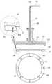
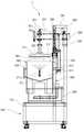
이하, 본 발명의 기본 구성의 실시 예로서, 제1 실시 예에 따른 반도체 웨이퍼의 에칭 장치의 각부 구성을 도 1 내지 도 3을 참고로 구체적으로 설명한다. 도 1은 에칭 장치의 정면도, 도 2는 에칭 장치의 측면도, 도 3은 에칭 장치 중 고정지그 및 구동축을 나타낸 도면이다.Hereinafter, as an embodiment of the basic configuration of the present invention, the configuration of each part of the etching apparatus of the semiconductor wafer according to the first embodiment will be described in detail with reference to FIGS. 1 is a front view of an etching apparatus, FIG. 2 is a side view of the etching apparatus, and FIG. 3 is a view showing a fixing jig and a drive shaft of the etching apparatus.
이에 따른 에칭 장치(1)를 개략적으로 살펴보면, 본체 부재(100); 에칭액을 분사시켜 웨이퍼(10)를 에칭하는 에칭 부재(200); 웨이퍼(10)를 에칭액의 분사 측으로 공급하여 에칭 작업을 수행되게 하는 웨이퍼 공급 부재(300);로 구성되고,Referring to the
여기서 본 발명의 에칭 장치(1)에 대한 각 구성들을 나누어 상세하게 설명하면 다음과 같다.Here, the components of the
먼저, 상기 본체 부재(100)는;First, the
에칭 장치(1)를 임의 위치에 설치되게 하며, 에칭 부재(200), 웨이퍼 공급 부재(300)를 지지하기 위한 것이다.The
예를 들면, 상기 본체 부재(100)는; 에칭 부재(200)의 설치공간을 제공하면서 웨이퍼 공급 부재(300)를 지지하는 메인프레임(110)을 더 포함한다.For example, the
상기 메인프레임(110)은 다수의 사각 빔 형태의 지지대를 서로 결합하여 하나의 사각 틀 형태인 메인프레임(110)을 제작하고, 사각 틀 형태로 제작된 메인프레임(110)의 내측으로 에칭 부재(200)의 설치를 위한 공간이 마련되고, 상기 메인프레임(110)의 상부로 웨이퍼 공급 부재(300)를 설치하여 지지되게 한다.The
이때, 상기 메인프레임(110)의 하단부에는 에칭 장치(1)를 간편하게 이동시키기 위한 캐스터 및 이동된 위치에서 에칭 장치(1)를 고정하기 위한 다리가 구비될 수 있다.In this case, a lower end of the
또한, 상기 본체 부재(100)는; 메인프레임(110)의 상부 일측으로 웨이퍼 공급 부재(300)를 결합하면서 상하 승강을 위한 작동공간(121)을 제공하는 한 쌍의 지지프레임(120)을 더 포함한다.In addition, the
상기 한 쌍의 지지프레임(120)은 메인프레임(110)의 상부 일측에 다수의 사각 빔 형태의 지지대를 서로 결합하여 사각 틀 형태로 제작하는데, 한 쌍의 지지프레임(120) 사이로 웨이퍼 공급 부재(300)가 결합되면서 상하 이동가능하게 하는 이격 공간으로 작동공간(121)이 마련되게 한다.The pair of
이때, 상기 한 쌍의 지지프레임(120)은 에칭 부재(200)의 제1수조(210)가 결합되는 측에 작동공간(121)이 마련되게 하여 웨이퍼 공급 부재(300)를 제1수조(210) 측에 인접하게 위치되게 한다.In this case, the pair of
한편, 상기 본체 부재(100)에는 에칭 장치(1)의 동작을 제어하기 위한 제어패널이 구비될 수 있다.On the other hand, the
그리고, 상기 에칭 부재(200)는;And, the
상기 본체 부재(100)에 에칭공간(214)을 제공하는데, 에칭액의 토출구(211a)가 상방으로 형성된 분사부(211)를 이용해 에칭액을 상향 분사시켜 웨이퍼(10)를 에칭하기 위한 것이다.An
예를 들면, 상기 에칭 부재(200)는; 웨이퍼 공급 부재(300)에 의해 웨이퍼(10)가 공급 수용되면서 에칭 작업을 수행하는 에칭공간(214)이 상향 개방되어 형성되고, 분사부(211)를 통해 분사되는 에칭액이 에칭 작업 후 에칭공간(214)에 모이게 하는 제1수조(210)를 더 포함한다.For example, the
상기 제1수조(210)는 본체 부재(100)의 메인프레임(110) 내측으로 지지프레임(120)의 하단부에 결합되는데, 상향 개방된 에칭공간(214)이 내측에 마련된 함체 형태로 제작되고, 하단부는 에칭공간(214)에 분사되는 에칭액이 모이도록 중앙으로 하향 집중되는 경사를 갖는다.The
여기서, 상기 제1수조(210)는 에칭공간(214)의 측방으로 관통삽입된 상태에서 복귀유로(230)에 연결되어 에칭액이 공급되고, 복귀유로(230)로부터 공급되는 에칭액을 제1수조(210) 내부에서 상향 분사시키는 분사부(211)를 더 포함한다.Here, the
상기 분사부(211)는 복귀유로(230)에 연결되는 파이프 형태로 제작되어 상측면에 다수의 토출구(211a)가 관통형성되고, 상기 분사부(211)가 제1수조(210)의 측방으로 에칭공간(214) 측에 관통삽입되어 에칭공간(214)에 위치되게 한다. 상기 분사부(211)가 제1수조(210)에 관통된 측은 에칭액의 누수를 방지하기 위해 기밀처리됨이 바람직하다.The
더불어, 제1수조(210)의 하단부에는 제2수조(220)와 연결되면서 에칭공간(214)에 모이는 에칭액을 제2수조(220) 측으로 회수되게 하는 회수유로(212)가 마련된다.In addition, a
상기 회수유로(212)는 파이프 형태로 일단을 제1수조(210)의 하단부에 연결되고, 타단부는 제2수조(220)이 상부 개방 측에 연결된다.The
이때, 상기 제1수조(210)에는 에칭공간(214)의 상부 개방측을 선택적으로 덮어 차폐하기 위한 덮개(213)가 마련되며, 상기 덮개(213)는 제1수조(210)의 상단 개방부를 덮을 수 있을 정도의 크기를 갖는 판재 형태로 제작되고, 웨이퍼 공급 부재(300)의 고정지그(310)가 에칭공간(213)을 드나드는 상태에서 덮개(213)를 덮을 수 있도록 중앙에 이에 대응하는 관통 구멍이 마련되고, 상기 덮개(213)를 덮은 상태에서 에칭 작업을 가능하게 한다.In this case, a
또한, 상기 에칭 부재(200)는; 제1수조(210)에 인접한 위치에서 회수유로(212)에 연결되어 마련되고, 상기 제1수조(210)에 모이는 에칭액이 상기 제1수조(210)와 연결된 회수유로(212)를 통해 회수되면서 저장되는 제2수조(220)를 더 포함한다.In addition, the
상기 제2수조(220)는 본체 부재(100)의 메인프레임(110) 내측으로 제1수조(210)에 인접한 측에 결합되는데, 상향 개방된 함체 형태로 제작되는데, 상기 제1수조(210)의 하단부에 마련된 복귀유로(230)의 일단이 제2수조(220)의 상부 개방 측에 연결되는 위치로 마련되어 제1수조(210)에 모이는 에칭액이 복귀유로(230)를 통해 제2수조(220)로 회수될 수 있다.The
이때, 상기 제2수조(220)의 하단부 일측에는 제2수조(220)에 저장된 에칭액을 필요에 따라 외부로 배출하기 위한 배출구(221)가 마련된다.At this time, a
또한, 상기 에칭 부재(200)는; 상기 제1수조(210)의 분사부(211)와 제2수조(220) 사이에 연결되며, 제1수조(210)에 구비된 분사부(211)로 제2수조(220)에 저장된 에칭액을 공급시켜 에칭액을 순환되게 하는 복귀유로(230)를 더 포함한다.In addition, the
상기 복귀유로(230)는 일단은 제1수조(210)의 측방에 연결되고 타단은 제2수조(220)의 측방에 각각 연결되는 파이프로 제작되어 제2수조(220)에 저장되는 에칭액을 제1수조(210)의 분사부(211) 측으로 공급할 수 있게 한다.The
이때, 상기 복귀유로(230)는 제2수조(220)에 저장된 에칭액을 강제 흡입 후 분사부(211) 측으로 공급시키는 펌프(231)가 마련되고, 상기 펌프(231)는 제2수조(220)와 복귀유로(230) 사이에 마련되며, 유체를 이송하기 위한 통상의 펌프를 적용할 수 있다. 상기 펌프(231)에는 에칭액의 여과를 위한 필터 기능이 부가될 수 있다.At this time, the
예컨대, 상기 제1수조(210), 제2수조(220), 회수유로(212), 복귀유로(230)로 이루어진 에칭 부재(200)의 순환 구조를 부가함에 따라 에칭 작업 중 분사되는 에칭액이 모이면서 회수되고, 회수된 에칭액은 다시 자동으로 복귀되어 분사부(211)에 공급됨으로 에칭액을 지속적으로 보충하지 않아 작업성이 향상되게 된다.For example, by adding a circulation structure of the
그리고, 상기 웨이퍼 공급 부재(300)는;And, the
상기 에칭 부재(200) 측에 인접하게 구비된 고정지그(310)를 이용해 웨이퍼(10)를 장착되게 하는데, 상기 고정지그(310)는 웨이퍼(10)의 에칭면을 상기 분사부(211)의 상부에서 하향 위치되게 하고, 상기 분사부(211)를 통해 에칭액이 분사되는 과정에서 웨이퍼(10)를 에칭공간(214)의 에칭액이 분사되는 측으로 공급 후 지지하여 에칭 작업을 수행되게 하는 것이다.The
예를 들면, 상기 웨이퍼 공급 부재(300)는; 웨이퍼(10)가 하단면에 장착되고, 장착된 웨이퍼(10)의 에칭면이 분사부(211)의 상부에서 하향 위치되게 하는 고정지그(310)를 더 포함한다.For example, the
상기 고정지그(310)는 원판 형태로 제작되면서 그 고정지그(310)의 하단면 내측에 웨이퍼(10)의 장착을 위한 장착부(312)가 홈으로 형성되고, 상기 고정지그(310)의 상측은 구동축(320)에 연결되면서 고정지그(310)가 에칭 부재(200)의 제1수조(210)에 인접한 측에서 본체 부재(100)에 지지된다.While the fixing
상기 장착부(312)는 웨이퍼(10)가 장착되는데, 바람직하게는 웨이퍼(10)가 조립되는 유동지그(360)가 결합되어 웨이퍼(10)를 장착되게 한다.The mounting
이때, 상기 고정지그(310)는 본체 부재(100)와 웨이퍼 공급 부재(300) 사이로 구비된 실린더(380)에 의해 승강 작동이 가능한데, 에칭 작업을 수행하면 제1수조(210) 측으로 하강하여 웨이퍼(10)가 에칭되게 하고, 에칭 작업이 완료되면 상승하여 제1수조(210)로부터 이탈된다.In this case, the fixing
여기서, 상기 고정지그(310)는 장착부(312)의 내측에 다수의 흡착공(311)이 관통 구멍으로 형성되며, 상기 흡착공(311)은 공기 흡입작용을 통해 장착부(312)에 삽입된 유동지그(360)를 흡착하여 고정되게 하기 위한 것이다.Here, the fixing
또한, 상기 웨이퍼 공급 부재(300)는; 복수의 고정팁(361)을 이용해 웨이퍼(10)를 고정되게 하며, 상기 고정팁(361)에 의해 고정된 웨이퍼(10)를 고정지그(310)에 조립하는 방식으로 웨이퍼(10)를 고정지그(310)에서 탈착 가능하게 장착시키는 유동지그(360)를 더 포함한다.In addition, the
상기 유동지그(360)는 장착부(312)에 삽입되어 결합 가능한 크기의 원판으로 제작되면서 하면에 웨이퍼(10)가 조립되는 공간을 제공하고, 유동지그(360)에 웨이퍼(10)가 조립되는 공간의 둘레로 복수의 고정팁(361)이 등간격으로 결합되면서 상기 복수의 고정팁(361)이 유동지그(360)에 조립되는 웨이퍼(10)의 일측면 둘레를 가압하여 고정되게 한다.The
이때, 상기 유동지그(360)는 여벌을 여러 개 만들어 사용할 수 있고, 여벌의 유동지그(360)에 각각 웨이퍼(10)를 조립한 상태에서 에칭 작업을 준비함으로 웨이퍼(10)를 연속으로 에칭 장치(1)에서 교체할 수 있게 한다.At this time, the
상기 고정팁(361)은 사각 블록 형태로 제작된 상태에서 유동지그(360)에 하나 이상 웨이퍼(10)가 조립되는 면에 등간격으로 결합되고, 상기 고정팁(361)이 유동지그(360)에 나사체결됨으로, 그 나사체결구조에 의해 웨이퍼(10)를 고정팁(361)이 압박하여 고정시킨다.The fixing
여기서, 상기 고정팁(361)은 웨이퍼(10)의 가압 측이 경사를 갖으면서 점 접촉 형태로 웨이퍼(10)를 가압되게 하는 경사면(361a)을 더 포함한다.Here, the fixing
상기 경사면(361a)은 웨이퍼(10)를 가압하는 고정팁(361)의 일측에 40°~ 50°경사를 갖는 면으로 형성되며, 상기 경사면(361a)에 의해 고정팁(361)에 웨이퍼(10)를 가압하는 면이 점 접촉 형태로 가압되면서 고정팁(361)에 웨이퍼(10)에 접촉되는 면적을 최소화하게 된다.The
예컨대, 상기 고정팁(361)에 의한 웨이퍼(10)의 점 접촉 구조를 제공함에 따라 웨이퍼(10)를 고정하기 위한 가압 면적을 최소화하여 에칭 작업 중 에칭면이 가려짐에 의한 작업의 번거로움을 해소하고, 웨이퍼(10)의 가압력이 적정 수준을 유지하여 웨이퍼(10)의 파손을 방지하게 된다.For example, by providing the point contact structure of the
이때, 상기 유동지그(360)는 얇은 두께의 웨이퍼(10)가 유동지그(360)의 하면에 밀착되어 조립됨으로 작업자가 웨이퍼(10)를 파지하기가 쉽지 않은데, 이를 해소하기 위해 웨이퍼(10)의 조립 측 내측면에 작업자의 손가락을 넣어서 웨이퍼(10)를 파지할 수 있게 하는 파지홈(362)이 마련된다.At this time, the
또한, 상기 웨이퍼 공급 부재(300)는; 고정지그(310)가 하단부에 결합되어 연결되고, 고정지그(310)이 연결 측 타단이 가이드프레임(330)에 결합되어 본체 부재(100)에 지지되는 구동축(320)을 더 포함한다.In addition, the
상기 구동축(320)은 환봉 형태로 제작되면, 수직으로 하단부는 고정지그(310)의 상측에 결합되고, 상단부는 본체 부재(100)에 지지되는 가이드프레임(330)에 연결되어 상기 고정지그(310)를 본체 부재(100)에 지지되게 한다.When the
이때, 상기 구동축(320)이 가이드프레임(330)에 결합된 측은 구동축(320)의 제자리 회전을 가이드하기 위한 베어링 등이 적용됨이 바람직하다.At this time, the
여기서, 상기 구동축(320)의 내측에는 고정지그(310)의 흡착공(311)과 통하는 중공의 공기유로(321)가 형성되고, 상기 공기유로(321)는 에어유닛(370)을 통해 전달되는 공기 흡입력을 흡착공(311)에 제공하기 위한 유로이며, 공기유로(321)의 상단부로 에어유닛(370)이 연결된다.Here, a
또한, 웨이퍼 공급 부재(300)는; 상기 구동축(320)에 연결되어 회전동력을 전달하는데, 상기 구동축(320)에 전달되는 회전동력을 이용해 고정지그(310)를 제자리 회전작동되게 하는 모터(340)를 더 포함한다.In addition, the
상기 모터(340)는 전기를 동력원으로 회전력을 제공하는 전동기이며, 모터(340)의 축이 벨트, 체인 등의 동력 연결 부재를 통해 구동축(320)의 상단부에 연결되면서 모터(340)의 회전 동력을 구동축(320)에 전달시켜, 그 구동축(320) 하단에 결합된 고정지그(310)를 제자리 회전 가능하게 한다.The
이때, 상기 모터(340)는 웨이퍼 공급 부재(300)를 본체 부재(100)에 지지하는 가이드프레임(330)에 결합된 상태에서 구동축(320)에 연결된다.In this case, the
특징적으로 상기 모터(340)가 구동축(320)에 연결됨에 따라 고정지그(310)가 제1수조(210)에 수용된 상태에서 에칭액이 분사부(211)를 통해 분사되는 에칭 과정에서 상기 모터(340)의 동력이 구동축(320)에 전달되어 고정지그(310)가 제자리 회전하게 된다.In particular, as the
예컨대, 상기 모터(340)를 부가함에 따라 에칭 중 고정지그(310)가 회전가능하여 웨이퍼(10)의 에칭이 균일하게 되면서 웨이퍼(10)에 분사된 에칭액을 웨이퍼(10)로부터 에칭 후 이탈시켜 에칭액에 의한 표면 불량을 방지하게 된다.For example, as the
또한, 상기 웨이퍼 공급 부재(300)는; 상기 구동축(320)의 공기유로(321)에 연결되면서 공기 흡입력을 공기유로(321)을 통해 흡착공(311)에 제공하여 고정지그(310)에 장착되는 유동지그(360)에 대한 고정력을 발휘되게 하는 에어유닛(370)을 더 포함한다.In addition, the
상기 에어유닛(370)은 구동축(320)의 공기유로(321) 상단부로 로터리피팅()을 이용해 연결되는데, 상기 로터리피팅()은 구동축(320)에 연결된 측이 헛돌면서 구동축(320)의 회전에 간섭 없이 공기 흡입력을 제공할 수 있도록 하며, 상기 로터리피팅()으로 공기 흡입을 위한 튜브가 결합되고, 로터리피팅()의 튜브에는 펌프와 같은 공기 흡입을 위한 기구가 연결되어 이루어진다.The
이때, 상기 로터리피팅()은 연결 측이 제자리 회전하면서 연결 기능을 수행하는 것이며, 바람직하게는 "SMC의 부품번호:KSL06-01S(로터리 피팅)"을 적용할 수 있고, 이와 동일 구성의 로터리 피팅이면 어느 것이든 적용하여도 무방하다.At this time, the rotary fitting () is to perform the connection function while the connection side rotates in place, preferably "Part Number: KSL06-01S (Rotary Fitting) of SMC" may be applied, and the rotary fitting of the same configuration Any of the following may be applied.
예컨대 상기 에어유닛(370)을 부가함에 따라 웨이퍼(10)가 결합된 유동지그(360)를 고정지그(310)에 공기 흡입력을 이용해 견고하게 고정되게 하고, 공기 흡입의 ON/OFF 조작으로 유동지그(360)를 간편하게 교체할 수 있게 된다.For example, as the
또한, 상기 웨이퍼 공급 부재(300)는; 고정지그(310)가 연결된 구동축(320)을 본체 부재(100)에 지지되게 하는 가이드프레임(330)을 더 포함한다.In addition, the
상기 가이드프레임(330)은 사각 프레임 형태로 한 쌍의 지지프레임(120) 사이의 작동공간(121)에 삽입된 상태에서 구동축(320)에 연결되는 고정지그(310)를 제1수조(210)에 수용 가능한 크기로 제작되며, 상기 가이드프레임(330)의 전방 측은 구동축(320)이 수직으로 결합되고, 가이드프레임(330)의 후방 측은 모터(340)가 구동축(320)에 벨트 연결되도록 결합된다.The
이때, 상기 가이드프레임(330)의 양측에는 가이드레일(350)의 직선 이동을 위한 러너가 본체 부재(100) 사이에서 결합되면서 가이드프레임(330)을 본체 부재(100)에 지지되게 한다.At this time, both sides of the
또한, 상기 웨이퍼 공급 부재(300)는; 상기 가이드프레임(330)과 본체 부재(100) 사이에 수직으로 결합되며, 가이드프레임(330)을 본체 부재(100)에 지지된 상태에서 상하 직선 이동을 가능하게 하는 가이드레일(350)을 더 포함한다.In addition, the
상기 가이드레일(350)은 직선 왕복 이동을 안내하기 위한 것이며, 직선형의 레일과 레일을 직선 이동하는 러너로 구성되고, 한 쌍의 가이드레일(350)이 한 쌍의 지지프레임(120) 내부 양측에 각각 수직으로 결합되는데, 가이드레일(350)의 레일 측은 본체 부재(100)에 결합되고 러너 측은 가이드프레임(330)에 결합되면서, 그 가이드프레임(330)을 본체 부재(100)에 지지되게 결합하면서 상하 수직으로 직선 이동되게 한다The
또한, 상기 웨이퍼 공급 부재(300)는; 상기 가이드프레임(330)에 신축 동력을 제공하여 가이드프레임(330)을 가이드레일(350)을 따라 승강되게 하는 실린더(380)를 더 포함한다.In addition, the
상기 실린더(380)는 유압 또는 공압에 의해 실린더 몸체에 구비된 로드가 신축 작동하면서 직선 이동을 위한 동력을 제공하는 것이며, 바람직하게는 공압을 이용하고, 상기 실린더(380)는 실린더 몸체 측이 본체 부재(100)의 메인프레임(110) 측에 수직으로 하단부가 결합되어 고정되고, 실린더(380)의 로드 측은 가이드프레임(330)의 하측 부분에 연결된다.The
이때, 상기 실린더(380)의 로드가 신축하면서 신축에 의한 직선 동력을 가이드프레임(330)에 전달하고, 그 실린더(380)의 동력에 의해 가이드프레임(330)이 가이드레일(350)을 따라서 승강 작동하게 된다.At this time, while the rod of the
특징적으로 상기 실린더(380)의 동력을 통해 가이드프레임(330)이 가이드레일(350)을 따라 승강 작동함에 따라 가이드프레임(330)에 구동축(320)을 통해 연결된 고정지그(310)가 실린더(380)의 동작에 따라 선택적으로 상승 또는 하강하여 고정지그(310)에 장착되는 웨이퍼(10)의 에칭 및 에칭 완료된 웨이퍼(10)의 분리작업을 간편하게 수행할 수 있다.In particular, as the
이하, 본 발명에 따른 반도체 웨이퍼의 에칭 장치의 작동 상태를 도 4 내지 도 5를 참고로 구체적으로 설명한다. 도 4는 에칭 장치의 에칭 전 상태도, 도 5는 에칭 장치의 에칭 작업의 상태도이다.Hereinafter, an operating state of an etching apparatus of a semiconductor wafer according to the present invention will be described in detail with reference to FIGS. 4 to 5. 4 is a state diagram before etching of the etching apparatus, and FIG. 5 is a state diagram of etching operations of the etching apparatus.
도 4에 따르면, 전술한 구조로 이루어진 에칭 장치(1)는 미리 준비된 유동지그(360)의 저면에 웨이퍼(10)를 고정팁(361)을 이용해 고정시켜 준비한다.According to FIG. 4, the
상기 웨이퍼 공급 부재(300)는 유동지그(360)에 고정된 웨이퍼(10)를 고정지그(310)에 장착시키기 위해 실린더(380)를 작동시켜 가이드프레임(330)에 구동축(320)을 통해 연결된 고정지그(310)를 제1수조(210) 상부로 이격되게 상승시킨다.The
이때, 상기 웨이퍼(10)가 준비된 유동지그(360)를 상기 제1수조(210) 상부로 이격된 상태의 고정지그(310) 저부에 장착시키는데, 웨이퍼(10)의 에칭면이 하향으로 위치되게 장착시켜 분사부(211)를 통해 상향 분사되는 에칭액에 대응하고, 상기 고정지그(310)에 장착된 유동지그(360)는 에어유닛(370)의 공기 흡착 작용을 통해 고정지그(310)에 고정된 상태로 에칭 준비를 수행한다.At this time, the
또한, 도 5에 따르면, 상기와 같이 고정지그(310)에 웨이퍼(10)가 고정된 유동지그(360)를 장착하여 에칭 준비를 하면, 작업자가 에칭 장치(1)를 작동시키는데, 이때 에칭 부재(200)에서는 제2수조(220)에 저장된 에칭액을 복귀유로(230)의 펌프(231)를 이용해 강제로 분사부(211) 측으로 공급하면서 분사부(211)의 토출구(211a)를 통해 에칭액이 제1수조(210) 내에서 상향 분사되도록 한다.In addition, according to FIG. 5, when the
상기 웨이퍼 공급 부재(300)는 실린더(380)가 작동되면서 가이드프레임(330)에 구동축(320)을 통해 연결된 고정지그(310)를 제1수조(210)의 내측으로 분사부(211)의 에칭액 분사 위치까지 하강시키고, 이 상태에서 모터(340)가 작동하면서 구동축(320)에 연결되 고정지그(310)를 회전시켜 에칭 작업을 수행되게 한다.The
한편, 상기 에칭 작업이 완료되면 고정지그(310)는 실린더(380)를 통해 제1수조(210) 상측으로 다시 상승한 후 미리 준비된 유동지그(360)를 교체하는 방식으로 에칭 작업을 연속적 수행한다.On the other hand, when the etching operation is completed, the fixing
이상 설명한 바와 같이. 본 발명은 특정의 바람직한 실시 예를 예시한 설명과 도면으로 표현하였으나, 여기서 사용하는 용어들은 본 발명을 용이하게 설명하기 위함이며, 이 용어들에 대한 의미 한정이나, 특허청구범위에 기재된 범위를 제한하기 위함이 아니며,As explained above. Although the invention has been shown in the description and drawings illustrating certain preferred embodiments, the terms used herein are intended to facilitate the description of the invention, the meanings limited to these terms and the scope of the claims are limited. Not for
본 발명은 상기한 실시 예에 따른 특허청구범위에 의해 나타난 발명의 사상 및 영역을 벗어나지 않는 범위 내에서 당해 발명이 속하는 기술 분야에서 통상의 지식을 가진 자에 의해 다양한 변경 및 개조, 수정 등이 가능할 수 있음을 누구나 쉽게 알 수 있을 것이다.The present invention may be variously modified, modified, modified, etc. by one of ordinary skill in the art without departing from the spirit and scope of the invention represented by the claims according to the above embodiments. Anyone can easily see that you can.
1; 에칭 장치 100; 본체 부재
110; 메인프레임 120; 지지프레임
200; 에칭 부재 210; 제1수로
220; 제2수로 230; 복귀유로
300; 웨이퍼 공급 부재 310; 고정지그
320; 구동축 330; 가이드프레임
340; 모터 350; 가이드레일
360; 유동지그 370; 에어유닛
380; 실린더One;
110;
200;
220;
300; A
320;
340;
360;
380; cylinder
Claims (5)
Translated fromKorean본체 부재(100)와;
상기 본체 부재(100)에 에칭공간(214)을 제공하는데, 에칭액의 토출구(211a)가 상방으로 형성된 분사부(211)를 이용해 에칭액을 상향 분사시켜 웨이퍼(10)를 에칭하는 에칭 부재(200)와;
상기 에칭 부재(200) 측에 인접하게 구비된 고정지그(310)를 이용해 웨이퍼(10)를 장착되게 하는데, 상기 고정지그(310)는 웨이퍼(10)의 에칭면을 상기 분사부(211)의 상부에서 하향 위치되게 하고, 상기 분사부(211)를 통해 에칭액이 분사되는 과정에서 웨이퍼(10)를 에칭공간(214)의 에칭액이 분사되는 측으로 공급 후 지지하여 에칭 작업을 수행되게 하는 웨이퍼 공급 부재(300)를 포함하여 구성되고,
상기 웨이퍼 공급 부재(300)는 복수의 고정팁(361)을 이용해 웨이퍼(10)를 고정되게 하며, 상기 고정팁(361)에 의해 고정된 웨이퍼(10)를 고정지그(310)에 조립하는 방식으로 웨이퍼(10)를 고정지그(310)에서 탈착 가능하게 장착시키는 유동지그(360)를 더 포함한 반도체 웨이퍼의 에칭 장치.An etching apparatus of a semiconductor wafer for etching a semiconductor wafer,
Body member 100;
An etching space 214 is provided in the main body member 100, and the etching member 200 is used to etch the wafer 10 by injecting the etching liquid upward using the spraying portion 211 having the ejection openings 211a formed thereon. Wow;
The wafer 10 is mounted by using the fixing jig 310 provided adjacent to the etching member 200, and the fixing jig 310 has an etching surface of the wafer 10 of the injection unit 211. The wafer supply member to be positioned downward from the upper side, and to support the wafer 10 to the side where the etching solution of the etching space 214 is injected after the etching solution is injected through the injection unit 211 to perform the etching operation 300, including
The wafer supply member 300 fixes the wafer 10 by using a plurality of fixing tips 361, and assembles the wafer 10 fixed by the fixing tips 361 to the fixing jig 310. And a flow jig (360) for detachably mounting the wafer (10) from the fixing jig (310).
상기 웨이퍼 공급 부재(300)는, 고정지그(310)가 하단부에 결합되는 구동축(320); 및,
상기 구동축(320)에 연결되어 회전동력을 전달하는데, 상기 구동축(320)에 전달되는 회전동력을 이용해 고정지그(310)를 제자리 회전작동되게 하는 모터(340)를 더 포함한 반도체 웨이퍼의 에칭 장치.The method of claim 1,
The wafer supply member 300 includes a drive shaft 320 to which the fixing jig 310 is coupled to the lower end; And,
And a motor (340) connected to the drive shaft (320) to transmit rotational power, wherein the fixed jig (310) is rotated in place by using the rotational power transmitted to the drive shaft (320).
상기 에칭 부재(200)는, 분사부(211)를 통해 분사되는 에칭액이 에칭 작업 후 에칭공간(214)에 모이는 제1수조(210)와;
상기 제1수조(210)에 모이는 에칭액이 상기 제1수조(210)와 연결된 회수유로(212)를 통해 회수되면서 저장되는 제2수조(220)와;
상기 제1수조(210)에 구비된 분사부(211)로 제2수조(220)에 저장된 에칭액을 공급시켜 에칭액을 순환되게 하는 복귀유로(230)를 더 포함한 반도체 웨이퍼의 에칭 장치.The method of claim 1,
The etching member 200 may include: a first bath 210 in which etching liquid injected through the injection unit 211 is collected in an etching space 214 after an etching operation;
A second tank 220 which is stored while the etching liquid collected in the first tank 210 is recovered through the recovery passage 212 connected to the first tank 210;
Etching apparatus further comprises a return passage 230 for supplying the etching liquid stored in the second tank 220 to the injection unit (211) provided in the first tank 210 to circulate the etching liquid.
상기 웨이퍼 공급 부재(300)는 고정지그(310)가 연결된 구동축(320) 부분을 본체 부재(100)에 지지한 상태에서 상하 승강 작동되게 하는 실린더(380)를 더 포함한 반도체 웨이퍼의 에칭 장치.The method of claim 1,
The wafer supply member 300 further includes a cylinder 380 for vertically raising and lowering operation in a state in which a support shaft 320 to which the fixing jig 310 is connected is supported on the body member 100.
Priority Applications (1)
| Application Number | Priority Date | Filing Date | Title |
|---|---|---|---|
| KR1020180094693AKR102085941B1 (en) | 2018-08-14 | 2018-08-14 | Etching device of semiconductor wafer |
Applications Claiming Priority (1)
| Application Number | Priority Date | Filing Date | Title |
|---|---|---|---|
| KR1020180094693AKR102085941B1 (en) | 2018-08-14 | 2018-08-14 | Etching device of semiconductor wafer |
Publications (2)
| Publication Number | Publication Date |
|---|---|
| KR20200019327A KR20200019327A (en) | 2020-02-24 |
| KR102085941B1true KR102085941B1 (en) | 2020-03-06 |
Family
ID=69637370
Family Applications (1)
| Application Number | Title | Priority Date | Filing Date |
|---|---|---|---|
| KR1020180094693AActiveKR102085941B1 (en) | 2018-08-14 | 2018-08-14 | Etching device of semiconductor wafer |
Country Status (1)
| Country | Link |
|---|---|
| KR (1) | KR102085941B1 (en) |
Families Citing this family (4)
| Publication number | Priority date | Publication date | Assignee | Title |
|---|---|---|---|---|
| CN114334703B (en)* | 2020-09-30 | 2025-06-24 | 矽磐微电子(重庆)有限公司 | An etching device |
| CN112635389B (en)* | 2020-12-28 | 2024-10-15 | 芯思杰技术(深圳)股份有限公司 | Etching jig, etching device and etching method |
| CN112687590B (en)* | 2021-01-08 | 2024-12-03 | 开化晶芯电子有限公司 | An etching device for semiconductor silicon wafer processing |
| CN114361072A (en)* | 2021-12-30 | 2022-04-15 | 江苏搏灵顿科技有限公司 | An automatic assembling semiconductor device etching device |
Citations (1)
| Publication number | Priority date | Publication date | Assignee | Title |
|---|---|---|---|---|
| JP2006070349A (en) | 2004-09-06 | 2006-03-16 | Renesas Technology Corp | Semiconductor fabrication equipment |
Family Cites Families (7)
| Publication number | Priority date | Publication date | Assignee | Title |
|---|---|---|---|---|
| JP2578569B2 (en) | 1993-06-30 | 1997-02-05 | 豊精密工業株式会社 | Chamfering method for spiral bevel gears |
| KR980010231A (en) | 1996-07-19 | 1998-04-30 | 구자홍 | Regenerative electric fan |
| US6115867A (en)* | 1997-08-18 | 2000-09-12 | Tokyo Electron Limited | Apparatus for cleaning both sides of substrate |
| KR100691212B1 (en)* | 2006-11-17 | 2007-03-12 | 애플티(주) | Semiconductor Wafer Cleaning Equipment and Semiconductor Wafer Manufacturing Equipment Using the Same |
| KR101038572B1 (en)* | 2009-06-05 | 2011-06-02 | 주식회사 엠엠테크 | Substrate Etching System with Vacuum Substrate Jig |
| KR20110010965A (en)* | 2009-07-27 | 2011-02-08 | 삼성전기주식회사 | Vertical Transfer Jig and Wet Etching Equipment Using It |
| JP5666414B2 (en)* | 2011-10-27 | 2015-02-12 | 東京エレクトロン株式会社 | Liquid processing apparatus, liquid processing method, and storage medium |
- 2018
- 2018-08-14KRKR1020180094693Apatent/KR102085941B1/enactiveActive
Patent Citations (1)
| Publication number | Priority date | Publication date | Assignee | Title |
|---|---|---|---|---|
| JP2006070349A (en) | 2004-09-06 | 2006-03-16 | Renesas Technology Corp | Semiconductor fabrication equipment |
Also Published As
| Publication number | Publication date |
|---|---|
| KR20200019327A (en) | 2020-02-24 |
Similar Documents
| Publication | Publication Date | Title |
|---|---|---|
| KR102085941B1 (en) | Etching device of semiconductor wafer | |
| KR100282160B1 (en) | Substrate treatment device and processing method | |
| JP5404196B2 (en) | Cleaning device | |
| CN110993524A (en) | Substrate post-processing device and method | |
| KR20200024552A (en) | Equipment For Collecting Dusts | |
| KR20140004087A (en) | Dye adsorption device, dye adsorption method, and substrate treatment apparatus | |
| KR20060059824A (en) | Vacuum drying equipment | |
| KR102041794B1 (en) | washing apparatus for parts | |
| JP6983602B2 (en) | Board processing equipment and board processing method | |
| CN218101191U (en) | Wafer cleaning device | |
| KR20100066010A (en) | Method and apparatus for cleaning and drying substrates | |
| KR20080026916A (en) | Substrate Dryer and Method | |
| CN115754020B (en) | Circulation type ultrasonic scanning detection system | |
| CN112452986A (en) | Automatic crucible cleaning equipment | |
| CN218452437U (en) | Circulation cleaning workstation | |
| KR100525601B1 (en) | Wet treating device | |
| TWI747580B (en) | Etching device | |
| CN214108211U (en) | Automatic crucible cleaning equipment | |
| KR102162310B1 (en) | Cleaning apparatus for plate glass | |
| CN114632751A (en) | Cleaning system | |
| JP3966848B2 (en) | Substrate processing equipment | |
| KR100360120B1 (en) | Cleansing apparatus | |
| CN220444592U (en) | Cleaning device | |
| CN220691967U (en) | Vertical wafer surface cleaning device | |
| KR102351749B1 (en) | Wafer cleanning apparatus |
Legal Events
| Date | Code | Title | Description |
|---|---|---|---|
| A201 | Request for examination | ||
| PA0109 | Patent application | Patent event code:PA01091R01D Comment text:Patent Application Patent event date:20180814 | |
| PA0201 | Request for examination | ||
| E902 | Notification of reason for refusal | ||
| PE0902 | Notice of grounds for rejection | Comment text:Notification of reason for refusal Patent event date:20190722 Patent event code:PE09021S01D | |
| E701 | Decision to grant or registration of patent right | ||
| PE0701 | Decision of registration | Patent event code:PE07011S01D Comment text:Decision to Grant Registration Patent event date:20191227 | |
| PG1501 | Laying open of application | ||
| GRNT | Written decision to grant | ||
| PR0701 | Registration of establishment | Comment text:Registration of Establishment Patent event date:20200302 Patent event code:PR07011E01D | |
| PR1002 | Payment of registration fee | Payment date:20200302 End annual number:3 Start annual number:1 | |
| PG1601 | Publication of registration | ||
| PR1001 | Payment of annual fee | Payment date:20240227 Start annual number:5 End annual number:5 | |
| PR1001 | Payment of annual fee | Payment date:20250224 Start annual number:6 End annual number:6 |