KR102085707B1 - Metal mask having a resin plate, vapor deposition mask, method for producing vapor deposition mask device, and method for producing organic semiconductor element - Google Patents
Metal mask having a resin plate, vapor deposition mask, method for producing vapor deposition mask device, and method for producing organic semiconductor elementDownload PDFInfo
- Publication number
- KR102085707B1 KR102085707B1KR1020197011496AKR20197011496AKR102085707B1KR 102085707 B1KR102085707 B1KR 102085707B1KR 1020197011496 AKR1020197011496 AKR 1020197011496AKR 20197011496 AKR20197011496 AKR 20197011496AKR 102085707 B1KR102085707 B1KR 102085707B1
- Authority
- KR
- South Korea
- Prior art keywords
- mask
- deposition mask
- resin
- deposition
- metal
- Prior art date
- Legal status (The legal status is an assumption and is not a legal conclusion. Google has not performed a legal analysis and makes no representation as to the accuracy of the status listed.)
- Active
Links
Images


Classifications
- H01L51/56—
- B—PERFORMING OPERATIONS; TRANSPORTING
- B05—SPRAYING OR ATOMISING IN GENERAL; APPLYING FLUENT MATERIALS TO SURFACES, IN GENERAL
- B05B—SPRAYING APPARATUS; ATOMISING APPARATUS; NOZZLES
- B05B12/00—Arrangements for controlling delivery; Arrangements for controlling the spray area
- B05B12/16—Arrangements for controlling delivery; Arrangements for controlling the spray area for controlling the spray area
- B05B12/20—Masking elements, i.e. elements defining uncoated areas on an object to be coated
- B—PERFORMING OPERATIONS; TRANSPORTING
- B05—SPRAYING OR ATOMISING IN GENERAL; APPLYING FLUENT MATERIALS TO SURFACES, IN GENERAL
- B05C—APPARATUS FOR APPLYING FLUENT MATERIALS TO SURFACES, IN GENERAL
- B05C21/00—Accessories or implements for use in connection with applying liquids or other fluent materials to surfaces, not provided for in groups B05C1/00 - B05C19/00
- B05C21/005—Masking devices
- B—PERFORMING OPERATIONS; TRANSPORTING
- B32—LAYERED PRODUCTS
- B32B—LAYERED PRODUCTS, i.e. PRODUCTS BUILT-UP OF STRATA OF FLAT OR NON-FLAT, e.g. CELLULAR OR HONEYCOMB, FORM
- B32B37/00—Methods or apparatus for laminating, e.g. by curing or by ultrasonic bonding
- B32B37/14—Methods or apparatus for laminating, e.g. by curing or by ultrasonic bonding characterised by the properties of the layers
- B32B37/16—Methods or apparatus for laminating, e.g. by curing or by ultrasonic bonding characterised by the properties of the layers with all layers existing as coherent layers before laminating
- B32B37/18—Methods or apparatus for laminating, e.g. by curing or by ultrasonic bonding characterised by the properties of the layers with all layers existing as coherent layers before laminating involving the assembly of discrete sheets or panels only
- B32B37/182—Methods or apparatus for laminating, e.g. by curing or by ultrasonic bonding characterised by the properties of the layers with all layers existing as coherent layers before laminating involving the assembly of discrete sheets or panels only one or more of the layers being plastic
- B—PERFORMING OPERATIONS; TRANSPORTING
- B32—LAYERED PRODUCTS
- B32B—LAYERED PRODUCTS, i.e. PRODUCTS BUILT-UP OF STRATA OF FLAT OR NON-FLAT, e.g. CELLULAR OR HONEYCOMB, FORM
- B32B38/00—Ancillary operations in connection with laminating processes
- B32B38/0008—Electrical discharge treatment, e.g. corona, plasma treatment; wave energy or particle radiation
- C—CHEMISTRY; METALLURGY
- C23—COATING METALLIC MATERIAL; COATING MATERIAL WITH METALLIC MATERIAL; CHEMICAL SURFACE TREATMENT; DIFFUSION TREATMENT OF METALLIC MATERIAL; COATING BY VACUUM EVAPORATION, BY SPUTTERING, BY ION IMPLANTATION OR BY CHEMICAL VAPOUR DEPOSITION, IN GENERAL; INHIBITING CORROSION OF METALLIC MATERIAL OR INCRUSTATION IN GENERAL
- C23C—COATING METALLIC MATERIAL; COATING MATERIAL WITH METALLIC MATERIAL; SURFACE TREATMENT OF METALLIC MATERIAL BY DIFFUSION INTO THE SURFACE, BY CHEMICAL CONVERSION OR SUBSTITUTION; COATING BY VACUUM EVAPORATION, BY SPUTTERING, BY ION IMPLANTATION OR BY CHEMICAL VAPOUR DEPOSITION, IN GENERAL
- C23C14/00—Coating by vacuum evaporation, by sputtering or by ion implantation of the coating forming material
- C23C14/04—Coating on selected surface areas, e.g. using masks
- C23C14/042—Coating on selected surface areas, e.g. using masks using masks
- C—CHEMISTRY; METALLURGY
- C23—COATING METALLIC MATERIAL; COATING MATERIAL WITH METALLIC MATERIAL; CHEMICAL SURFACE TREATMENT; DIFFUSION TREATMENT OF METALLIC MATERIAL; COATING BY VACUUM EVAPORATION, BY SPUTTERING, BY ION IMPLANTATION OR BY CHEMICAL VAPOUR DEPOSITION, IN GENERAL; INHIBITING CORROSION OF METALLIC MATERIAL OR INCRUSTATION IN GENERAL
- C23C—COATING METALLIC MATERIAL; COATING MATERIAL WITH METALLIC MATERIAL; SURFACE TREATMENT OF METALLIC MATERIAL BY DIFFUSION INTO THE SURFACE, BY CHEMICAL CONVERSION OR SUBSTITUTION; COATING BY VACUUM EVAPORATION, BY SPUTTERING, BY ION IMPLANTATION OR BY CHEMICAL VAPOUR DEPOSITION, IN GENERAL
- C23C14/00—Coating by vacuum evaporation, by sputtering or by ion implantation of the coating forming material
- C23C14/22—Coating by vacuum evaporation, by sputtering or by ion implantation of the coating forming material characterised by the process of coating
- C23C14/24—Vacuum evaporation
- C—CHEMISTRY; METALLURGY
- C23—COATING METALLIC MATERIAL; COATING MATERIAL WITH METALLIC MATERIAL; CHEMICAL SURFACE TREATMENT; DIFFUSION TREATMENT OF METALLIC MATERIAL; COATING BY VACUUM EVAPORATION, BY SPUTTERING, BY ION IMPLANTATION OR BY CHEMICAL VAPOUR DEPOSITION, IN GENERAL; INHIBITING CORROSION OF METALLIC MATERIAL OR INCRUSTATION IN GENERAL
- C23F—NON-MECHANICAL REMOVAL OF METALLIC MATERIAL FROM SURFACE; INHIBITING CORROSION OF METALLIC MATERIAL OR INCRUSTATION IN GENERAL; MULTI-STEP PROCESSES FOR SURFACE TREATMENT OF METALLIC MATERIAL INVOLVING AT LEAST ONE PROCESS PROVIDED FOR IN CLASS C23 AND AT LEAST ONE PROCESS COVERED BY SUBCLASS C21D OR C22F OR CLASS C25
- C23F1/00—Etching metallic material by chemical means
- C23F1/02—Local etching
- G—PHYSICS
- G03—PHOTOGRAPHY; CINEMATOGRAPHY; ANALOGOUS TECHNIQUES USING WAVES OTHER THAN OPTICAL WAVES; ELECTROGRAPHY; HOLOGRAPHY
- G03F—PHOTOMECHANICAL PRODUCTION OF TEXTURED OR PATTERNED SURFACES, e.g. FOR PRINTING, FOR PROCESSING OF SEMICONDUCTOR DEVICES; MATERIALS THEREFOR; ORIGINALS THEREFOR; APPARATUS SPECIALLY ADAPTED THEREFOR
- G03F7/00—Photomechanical, e.g. photolithographic, production of textured or patterned surfaces, e.g. printing surfaces; Materials therefor, e.g. comprising photoresists; Apparatus specially adapted therefor
- G03F7/20—Exposure; Apparatus therefor
- H—ELECTRICITY
- H01—ELECTRIC ELEMENTS
- H01L—SEMICONDUCTOR DEVICES NOT COVERED BY CLASS H10
- H01L21/00—Processes or apparatus adapted for the manufacture or treatment of semiconductor or solid state devices or of parts thereof
- H01L21/02—Manufacture or treatment of semiconductor devices or of parts thereof
- H01L21/027—Making masks on semiconductor bodies for further photolithographic processing not provided for in group H01L21/18 or H01L21/34
- H01L51/0011—
- H—ELECTRICITY
- H05—ELECTRIC TECHNIQUES NOT OTHERWISE PROVIDED FOR
- H05B—ELECTRIC HEATING; ELECTRIC LIGHT SOURCES NOT OTHERWISE PROVIDED FOR; CIRCUIT ARRANGEMENTS FOR ELECTRIC LIGHT SOURCES, IN GENERAL
- H05B33/00—Electroluminescent light sources
- H05B33/10—Apparatus or processes specially adapted to the manufacture of electroluminescent light sources
- H—ELECTRICITY
- H10—SEMICONDUCTOR DEVICES; ELECTRIC SOLID-STATE DEVICES NOT OTHERWISE PROVIDED FOR
- H10K—ORGANIC ELECTRIC SOLID-STATE DEVICES
- H10K71/00—Manufacture or treatment specially adapted for the organic devices covered by this subclass
- H—ELECTRICITY
- H10—SEMICONDUCTOR DEVICES; ELECTRIC SOLID-STATE DEVICES NOT OTHERWISE PROVIDED FOR
- H10K—ORGANIC ELECTRIC SOLID-STATE DEVICES
- H10K71/00—Manufacture or treatment specially adapted for the organic devices covered by this subclass
- H10K71/10—Deposition of organic active material
- H10K71/16—Deposition of organic active material using physical vapour deposition [PVD], e.g. vacuum deposition or sputtering
- H10K71/166—Deposition of organic active material using physical vapour deposition [PVD], e.g. vacuum deposition or sputtering using selective deposition, e.g. using a mask
- B—PERFORMING OPERATIONS; TRANSPORTING
- B32—LAYERED PRODUCTS
- B32B—LAYERED PRODUCTS, i.e. PRODUCTS BUILT-UP OF STRATA OF FLAT OR NON-FLAT, e.g. CELLULAR OR HONEYCOMB, FORM
- B32B2310/00—Treatment by energy or chemical effects
- B32B2310/08—Treatment by energy or chemical effects by wave energy or particle radiation
- B32B2310/0806—Treatment by energy or chemical effects by wave energy or particle radiation using electromagnetic radiation
- B32B2310/0843—Treatment by energy or chemical effects by wave energy or particle radiation using electromagnetic radiation using laser
- B—PERFORMING OPERATIONS; TRANSPORTING
- B32—LAYERED PRODUCTS
- B32B—LAYERED PRODUCTS, i.e. PRODUCTS BUILT-UP OF STRATA OF FLAT OR NON-FLAT, e.g. CELLULAR OR HONEYCOMB, FORM
- B32B2311/00—Metals, their alloys or their compounds
- B—PERFORMING OPERATIONS; TRANSPORTING
- B32—LAYERED PRODUCTS
- B32B—LAYERED PRODUCTS, i.e. PRODUCTS BUILT-UP OF STRATA OF FLAT OR NON-FLAT, e.g. CELLULAR OR HONEYCOMB, FORM
- B32B2398/00—Unspecified macromolecular compounds
- H—ELECTRICITY
- H10—SEMICONDUCTOR DEVICES; ELECTRIC SOLID-STATE DEVICES NOT OTHERWISE PROVIDED FOR
- H10K—ORGANIC ELECTRIC SOLID-STATE DEVICES
- H10K50/00—Organic light-emitting devices
- H10K50/10—OLEDs or polymer light-emitting diodes [PLED]
- H10K50/11—OLEDs or polymer light-emitting diodes [PLED] characterised by the electroluminescent [EL] layers
Landscapes
- Chemical & Material Sciences (AREA)
- Engineering & Computer Science (AREA)
- Manufacturing & Machinery (AREA)
- Chemical Kinetics & Catalysis (AREA)
- Materials Engineering (AREA)
- Mechanical Engineering (AREA)
- Metallurgy (AREA)
- Organic Chemistry (AREA)
- Physics & Mathematics (AREA)
- General Physics & Mathematics (AREA)
- Plasma & Fusion (AREA)
- Thermal Sciences (AREA)
- Condensed Matter Physics & Semiconductors (AREA)
- Computer Hardware Design (AREA)
- Microelectronics & Electronic Packaging (AREA)
- Power Engineering (AREA)
- General Chemical & Material Sciences (AREA)
- Physical Vapour Deposition (AREA)
- Electroluminescent Light Sources (AREA)
Abstract
Translated fromKoreanDescription
Translated fromKorean본 발명은 증착 마스크를 제조하기 위해 사용되는 수지판을 구비한 금속 마스크에 관한 것이다. 본 발명은 또한 증착 마스크, 증착 마스크 장치의 제조 방법, 및 유기 반도체 소자의 제조 방법에 관한 것이다.The present invention relates to a metal mask with a resin plate used to produce a deposition mask. The present invention also relates to a deposition mask, a method of manufacturing a deposition mask apparatus, and a method of manufacturing an organic semiconductor device.
종래, 유기 EL 소자의 제조에 있어서, 유기 EL 소자의 유기층 또는 캐소드 전극의 형성에는, 예를 들면, 증착해야 할 영역에 다수의 미세한 슬릿(slit)을 미소 간격으로 평행하게 배열하여 이루어지는 금속으로 구성되는 증착 마스크가 사용되고 있었다. 이 증착 마스크를 사용하는 경우, 증착해야 할 기판 표면에 증착 마스크를 탑재하고, 이면(裏面)에서 자석을 사용하여 유지시키고 있지만, 슬릿의 강성은 극히 작아서, 증착 마스크를 기판 표면에 유지할 때 슬릿에 왜곡(distortion)이 생기기 쉽고, 고정밀도화 또는 슬릿 길이가 커지는 제품의 대형화의 장해가 되었다.Conventionally, in the manufacture of an organic EL device, in forming an organic layer or a cathode of the organic EL device, for example, a plurality of fine slits are arranged in parallel to each other at minute intervals in a region to be deposited. The deposition mask which was used was used. In the case of using this deposition mask, the deposition mask is mounted on the substrate surface to be deposited and is held by a magnet on the back surface. However, the slit rigidity is extremely small, so that when the deposition mask is held on the substrate surface, Distortion tends to occur, and it becomes a obstacle of the enlargement of the product which becomes high precision or the slit length becomes large.
슬릿의 왜곡을 방지하기 위한 증착 마스크에 대하여는, 각종 검토가 이루어져 있고, 예를 들면, 특허문헌 1에는, 복수의 개구부를 구비한 제1 금속 마스크를 겸하는 베이스 플레이트(base plate)와, 상기 개구부를 덮는 영역에 다수의 미세한 슬릿을 구비한 제2 금속 마스크와, 제2 금속 마스크를 슬릿의 길이 방향으로 인장(引張)시킨 상태로 베이스 플레이트 상에 위치시키는 마스크 인장 유지 수단을 구비한 증착 마스크가 제안되어 있다. 즉, 2종의 금속 마스크를 조합한 증착 마스크가 제안되어 있다. 이 증착 마스크에 의하면, 슬릿에 왜곡이 발생시키지 않고 슬릿 정밀도를 확보할 수 있도록 되어 있다.Various examinations are made about the vapor deposition mask for preventing the distortion of a slit, For example, in
그런데, 최근, 유기 EL 소자를 사용한 제품의 대형화 또는 기판 크기의 대형화에 따라, 증착 마스크에 대하여도 대형화의 요청이 높아지고 있고, 금속으로 구성되는 증착 마스크의 제조에 사용되는 금속판도 대형화되고 있다. 그러나, 현재의 금속 가공 기술로는, 대형의 금속판에 슬릿을 양호한 정밀도로 형성하는 것은 곤란하고, 설령 상기 특허문헌 1에 제안되어 있는 방법 등에 의해 슬릿부의 왜곡을 방지할 수 있었다고 해도, 슬릿의 고정밀도화에 대한 대응은 불가능하다. 또한, 금속만으로 이루어지는 증착 마스크로 한 경우에는, 대형화에 따라 그 질량도 증대하고, 프레임을 포함한 총 질량도 증대하므로 취급에 지장을 초래하게 된다.By the way, in recent years, with the increase of the size of the product which used organic electroluminescent element, or the size of the board | substrate, the request for enlargement also increases with respect to a vapor deposition mask, and the metal plate used for manufacture of the vapor deposition mask which consists of metals is also increasing. However, with the current metal working technology, it is difficult to form slits on a large metal plate with good precision, and even if the distortion of the slit portions can be prevented by the method proposed in the
본 발명은 이와 같은 상황을 감안하여 이루어진 것이며, 경량화를 도모할 수 있는, 증착 마스크를 제조하기 위해 사용되는 수지판을 구비한 금속 마스크를 제공하는 것을 과제로 한다.This invention is made | formed in view of such a situation, and makes it a subject to provide the metal mask provided with the resin plate used for manufacturing a vapor deposition mask which can aim at weight reduction.
또한 본 발명은 대형화한 경우라도 고정밀도화와 경량화를 모두 만족시킬 수 있는 증착 마스크를 제공하는 것, 및 이 증착 마스크를 프레임에 양호한 정밀도로 위치맞춤시킬 수 있는 증착 마스크 장치의 제조 방법을 제공하는 것, 또한 유기 반도체 소자를 양호한 정밀도로 제조할 수 있는 유기 반도체 소자의 제조 방법을 제공하는 것을 과제로 한다.In addition, the present invention provides a deposition mask capable of satisfying both high precision and light weight even in a large size, and providing a method of manufacturing a deposition mask apparatus capable of aligning the deposition mask with a frame with good precision. Another object of the present invention is to provide a method for producing an organic semiconductor element, which can produce an organic semiconductor element with good accuracy.
상기 과제를 해결하기 위한 본 발명은 수지판을 구비한 금속 마스크로서, 슬릿이 설치된 금속 마스크와, 상기 금속 마스크의 표면에 위치하고 상기 슬릿과 중첩하는 위치에 증착 제작하는 패턴에 대응한 개구부가 종횡으로 복수 열 배치된 수지 마스크가, 적층되어 이루어지는 증착 마스크를 제조하기 위해 사용되는 것이며, 슬릿이 설치된 금속 마스크의 한쪽 면에 수지판이 설치되어 이루어지는 것을 특징으로 한다.MEANS TO SOLVE THE PROBLEM In order to solve the said subject, this invention is a metal mask provided with a resin plate, Comprising: The metal mask provided with the slit, and the opening part corresponding to the pattern which deposits and manufactures in the position which overlaps with the said slit on the surface of the said metal mask are vertically and horizontally. A resin mask arranged in plural rows is used to manufacture a deposition mask formed by lamination, and a resin plate is provided on one surface of a metal mask provided with slits.
또한, 상기 과제를 해결하기 위한 본 발명은, 증착 마스크로서, 슬릿이 설치된 금속 마스크; 및 상기 금속 마스크의 표면에 위치하고, 증착 제작하는 패턴에 대응한 개구부가 종횡(縱橫)으로 복수 열 배치된 수지 마스크가 적층되어 이루어지는 것을 특징으로 한다.In addition, the present invention for solving the above problems, a deposition mask, a metal mask provided with a slit; And a resin mask which is disposed on the surface of the metal mask and has a plurality of rows of openings corresponding to the pattern to be deposited and fabricated in a vertical and horizontal direction.
또한, 상기 금속 마스크가 자성체이어도 된다. 또한, 상기 개구부의 단면(斷面) 형상이 증착원 방향을 향해 넓어지는 부분을 가지고 있어도 된다. 상기 슬릿의 단면 형상이 증착원 방향을 향해 넓어지는 부분을 가지고 있어도 된다. 또한, 상기 금속 마스크의 슬릿과 상기 수지 마스크의 개구부에 의해 형성되는 개구 전체의 단면 형상이 계단형을 이루고 있어도 된다.In addition, the metal mask may be a magnetic material. Moreover, you may have the part which the cross-sectional shape of the said opening part spreads toward a vapor deposition source direction. The slit may have a portion where the cross-sectional shape of the slit widens toward the deposition source direction. Moreover, the cross-sectional shape of the whole opening formed by the slit of the said metal mask and the opening of the said resin mask may be stepped.
또한, 상기 수지 마스크의 상기 개구부를 형성하는 단면에 배리어층(barrier layer)이 형성되어 있어도 된다. 또한, 상기 수지 마스크의 두께가 3㎛ 이상 25㎛ 이하라도 된다.Furthermore, a barrier layer may be formed in the end surface which forms the said opening part of the said resin mask. Moreover, the thickness of the said resin mask may be 3 micrometers or more and 25 micrometers or less.
상기 과제를 해결하기 위한 본 발명은 증착 마스크 장치의 제조 방법으로서, 슬릿이 설치된 금속 마스크와, 수지판을 접합하는 단계; 금속을 포함하는 프레임 위에, 상기 수지판이 접합된 금속 마스크를 고정하는 단계; 및 상기 금속 마스크 측으로부터 레이저를 조사하고, 상기 수지판에 증착 제작하는 패턴에 대응한 개구부를 종횡으로 복수 열 형성하는 단계를 포함한 것을 특징으로 한다.The present invention for solving the above problems is a method of manufacturing a deposition mask device, comprising the steps of: bonding a metal mask and a resin plate provided with a slit; Fixing a metal mask to which the resin plate is bonded onto a frame including metal; And irradiating a laser from the metal mask side, and forming a plurality of rows vertically and horizontally in openings corresponding to patterns formed by vapor deposition on the resin plate.
또한, 상기 과제를 해결하기 위한 본 발명은 증착 마스크 장치의 제조 방법으로서, 금속을 포함하는 프레임 위에, 슬릿이 설치된 금속 마스크를 고정하는 단계; 상기 프레임에 고정된 금속 마스크와 수지판을 접합하는 단계; 및 상기 금속 마스크 측으로부터 레이저를 조사하고, 상기 수지판에 증착 제작하는 패턴에 대응한 개구부를 종횡으로 복수 열 형성하는 단계를 포함한 것을 특징으로 한다.In addition, the present invention for solving the above problems is a method of manufacturing a deposition mask device, the step of fixing a metal mask, the slit is installed on a frame containing a metal; Bonding a metal mask and a resin plate fixed to the frame; And irradiating a laser from the metal mask side, and forming a plurality of rows vertically and horizontally in openings corresponding to patterns formed by vapor deposition on the resin plate.
또한, 상기 과제를 해결하기 위한 본 발명은 유기 반도체 소자의 제조 방법으로서, 상기 특징의 증착 마스크가 사용되는 것을 특징으로 한다.In addition, the present invention for solving the above problems is characterized in that the deposition mask of the above characteristics is used as a method of manufacturing an organic semiconductor device.
본 발명의 수지판을 구비한 금속 마스크에 의하면, 경량화를 도모할 수 있다.According to the metal mask provided with the resin plate of this invention, weight reduction can be aimed at.
또한, 본 발명의 증착 마스크에 의하면, 대형화한 경우에도 고정밀도화와 경량화를 모두 만족시킬 수 있다. 또한, 본 발명의 증착 마스크 장치의 제조 방법에 의하면, 상기 증착 마스크의 효과에 더하여, 상기한 증착 마스크를 프레임에 양호한 정밀도로 위치맞춤시킬 수 있다.. 또한, 본 발명의 유기 반도체 소자의 제조 방법에 의하면, 유기 반도체 소자를 양호한 정밀도로 제조할 수 있다.Moreover, according to the vapor deposition mask of this invention, even if it enlarges, it can satisfy both high precision and weight reduction. Moreover, according to the manufacturing method of the vapor deposition mask apparatus of this invention, in addition to the effect of the said vapor deposition mask, the said vapor deposition mask can be positioned in a frame with high precision. Moreover, the manufacturing method of the organic-semiconductor element of this invention. According to the present invention, the organic semiconductor element can be manufactured with good accuracy.
도 1은 본 발명의 일례를 나타낸 증착 마스크의 금속 마스크와 수지 마스크를 분해하여 나타낸 개략 사시도이며, (a)는 금속 마스크의 개략 사시도이고, (b)는 수지 마스크의 개략 사시도이다.
도 2 (a), (c), (d)는 본 발명의 일례를 나타낸 증착 마스크의 금속 마스크 측에서 본 정면도이며, (b)는 본 발명의 일례를 나타낸 증착 마스크를 나타낸 개략 단면도이다.
도 3은 본 발명의 증착 마스크(100)의 확대 단면도이다.
도 4 (a)는 수지 마스크의 다른 태양(態樣)의 사시도이며, (b)는 그 단면도이다.
도 5는 본 발명의 증착 마스크(100)의 다른 태양을 나타낸 정면도이다.
도 6은 제1 제조 방법을 설명하기 위한 공정도이다. 그리고 (a)∼(f)는 모두 단면도이다.
도 7은 제2 제조 방법을 설명하기 위한 공정도이다. 그리고 (a)∼(f)는 모두 단면도이다.
도 8은 섀도(shadow)와 금속 마스크의 두께와의 관계를 나타낸 개략 단면도이다.
도 9는 금속 마스크의 슬릿과 수지 마스크의 개구부와의 관계를 나타낸 부분 개략 단면도이다.
도 10은 금속 마스크의 슬릿과 수지 마스크의 개구부와의 관계를 나타낸 부분 개략 단면도이다.BRIEF DESCRIPTION OF THE DRAWINGS The schematic perspective view which decomposes the metal mask and resin mask of the vapor deposition mask which showed an example of this invention, (a) is a schematic perspective view of a metal mask, (b) is a schematic perspective view of a resin mask.
(A), (c), (d) is the front view seen from the metal mask side of the vapor deposition mask which showed an example of this invention, (b) is schematic sectional drawing which shows the vapor deposition mask which showed an example of this invention.
3 is an enlarged cross-sectional view of the
Fig. 4A is a perspective view of another embodiment of the resin mask, and Fig. 4B is a sectional view thereof.
5 is a front view showing another aspect of the
6 is a flowchart for explaining a first manufacturing method. And (a)-(f) is sectional drawing in all.
7 is a flowchart for explaining a second manufacturing method. And (a)-(f) is sectional drawing in all.
8 is a schematic cross-sectional view showing the relationship between the shadow and the thickness of the metal mask.
9 is a partial schematic cross-sectional view showing the relationship between the slit of the metal mask and the opening of the resin mask.
10 is a partial schematic cross-sectional view showing the relationship between the slit of the metal mask and the opening of the resin mask.
이하에, 본 발명의 증착 마스크(100)에 대하여 도면을 참조하여 구체적으로 설명한다.EMBODIMENT OF THE INVENTION Below, the
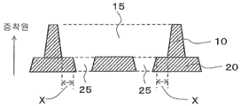
도 1 (a)는 본 발명의 일례를 나타낸 증착 마스크를 구성하는 금속 마스크의 개략 사시도이며, 도 1 (b)는 본 발명의 일례를 나타낸 증착 마스크를 구성하는 수지 마스크의 개략 사시도이다. 도 2 (a)는 본 발명의 일례를 나타낸 증착 마스크의 금속 마스크 측에서 본 정면도이며, 도 2 (b)는 본 발명의 일례를 나타낸 증착 마스크를 나타낸 개략 단면도이다. 도 3은 본 발명의 증착 마스크(100)의 확대 단면도이다. 그리고, 도 1∼도 3 모두, 금속 마스크의 형성된 슬릿 및 증착 마스크에 형성된 개구부를 강조하기 위해, 전체에 대한 비율을 크게 기재하고 있다.FIG. 1 (a) is a schematic perspective view of a metal mask constituting a vapor deposition mask showing an example of the present invention, and FIG. 1 (b) is a schematic perspective view of a resin mask constituting a vapor deposition mask showing an example of the present invention. Fig. 2 (a) is a front view seen from the metal mask side of the deposition mask showing one example of the present invention, and Fig. 2 (b) is a schematic cross-sectional view showing the deposition mask showing an example of the present invention. 3 is an enlarged cross-sectional view of the
도 1, 2에 나타낸 바와 같이, 본 발명의 증착 마스크(100)는, 슬릿(15)이 형성된 금속 마스크(10)와, 금속 마스크(10)의 표면(도 2 (b)에 나타낸 경우에 있어서는, 금속 마스크(10)의 하면)에 위치하고, 증착 제작하는 패턴에 대응한 개구부(25)가 종횡으로 복수 열 배치된 수지 마스크(20)가 적층된 구성을 취한다.As shown in Figs. 1 and 2, the
여기서, 본 발명의 증착 마스크(100)의 질량과 종래 공지의 금속만으로 구성되는 증착 마스크의 질량을, 증착 마스크 전체의 두께가 동일하다고 가정하여 비교하면, 종래 공지의 증착 마스크의 금속 재료의 일부를 수지 재료에 치환한 분만큼, 본 발명의 증착 마스크(100)의 질량은 가벼워진다. 또한, 금속만으로 구성되는 증착 마스크를 사용하여, 경량화를 도모하기 위해서는, 그 증착 마스크의 두께를 얇게 할 필요 등이 있지만, 증착 마스크의 두께를 얇게 한 경우에는, 증착 마스크를 대형화할 때, 증착 마스크에 왜곡이 발생하는 경우나, 내구성(耐久性)이 저하되는 경우가 발생한다. 한편, 본 발명의 증착 마스크에 의하면, 대형화할 때의 왜곡이나, 내구성을 만족시키기 위하여, 증착 마스크 전체의 두께를 두껍게 한 경우라도, 수지 마스크(20)의 존재에 의하여, 금속만으로 형성되는 증착 마스크보다 경량화를 도모할 수 있다. 이하, 각각에 대하여 구체적으로 설명한다.Here, when the mass of the
(수지 마스크)(Resin mask)
수지 마스크(20)는 수지로 구성되며, 도 1, 2에 나타낸 바와 같이, 슬릿(15)과 중첩되는 위치에 증착 제작하는 패턴에 대응한 개구부(25)가 종횡으로 복수 열 배치되어 있다. 그리고, 본원 명세서에 있어서 증착 제작하는 패턴이란, 해당 증착 마스크를 사용하여 제작하려는 패턴을 의미하고, 예를 들면, 그 증착 마스크를 유기 EL 소자의 유기층의 형성에 사용하는 경우에는, 그 유기층의 형상이다. 또한, 본 발명에서는, 개구부가 종횡으로 복수 열 배치된 예를 들어 설명을 하고 있지만, 개구부(25)는 슬릿과 중첩되는 위치에 설치되어 있으면 되고, 슬릿(15)이 세로 방향, 또는 가로 방향으로 1열만 배치되어 있는 경우에는, 그 1열의 슬릿(15)과 중첩되는 위치에 개구부(25)가 설치되어 있으면 된다.The
수지 마스크(20)는, 종래 공지의 수지 재료를 적절히 선택해 사용할 수 있고, 그 재료에 대하여 특별히 한정되지 않지만, 레이저 가공 등에 의해 고정밀도의 개구부(25)의 형성이 가능하며, 열이나 시간 경과에서의 치수 변화율이나 흡습율이 작고, 경량인 재료를 사용하는 것이 바람직하다. 이와 같은 재료로서는, 폴리이미드 수지, 폴리아미드 수지, 폴리아미드이미드 수지, 폴리에스테르 수지, 폴리에틸렌 수지, 폴리비닐알코올 수지, 폴리프로필렌 수지, 폴리카보네이트 수지, 폴리스티렌 수지, 폴리 아크릴로니트릴 수지, 에틸렌 아세트산 비닐 공중합체 수지, 에틸렌-비닐 알코올 공중합체 수지, 에틸렌-메타크릴산 공중합체 수지, 폴리염화비닐 수지, 폴리 염화 비닐리덴 수지, 셀로판, 아이오노머 수지((ionomer resin) 등을 들 수 있다. 상기에 예시한 재료 중에서도, 그 열팽창 계수가 16ppm/℃ 이하인 수지 재료가 바람직하고, 흡습 비율이 1.0%이하인 수지 재료가 바람직하고, 이 양쪽의 조건을 구비하는 수지 재료가 특히 바람직하다. 본 발명에서는, 수지 마스크(20)가 전술한 바와 같이 금속 재료에 비해, 고정밀도의 개구부(25)의 형성이 가능한 수지 재료로 구성된다. 따라서, 고정밀도의 개구부(25)를 가지는 증착 마스크(100)로 할 수 있다.The
수지 마스크(20)의 두께에 대해도 특별히 한정은 없지만, 본 발명의 증착 마스크(100)를 사용하여 증착을 행했을 때, 증착 작성하는 패턴에 불충분한 증착 부분, 즉 목적으로 하는 증착 막 두께보다 얇은 막 두께가 되는 증착 부분, 이른바 섀도가 생기는 것을 방지하기 위해서는, 수지 마스크(20)는 가능한 한 얇은 것이 바람직하다. 그러나, 수지 마스크(20)의 두께가 3㎛ 미만인 경우에는, 핀홀(pinhole) 등의 결함이 생기기 쉽고, 또한 변형 등의 리스크가 높아진다. 한편, 25㎛를 넘으면 섀도의 발생이 생길 수 있다. 이 점을 고려하면 수지 마스크(20)의 두께는 3㎛ 이상 25㎛ 이하인 것이 바람직하다. 수지 마스크(20)의 두께를 이 범위 내로 함으로써, 핀홀 등의 결함이나 변형 등의 리스크를 감소시킬 수 있고, 또한 섀도의 발생을 효과적으로 방지할 수 있다. 특히, 수지 마스크(20)의 두께를, 3㎛ 이상 10㎛ 이하, 더욱 바람직하게는 4㎛ 이상 8㎛ 이하로 함으로써, 300ppi를 초과하는 고정밀도 패턴을 형성할 때의 섀도의 영향을 더욱 효과적으로 방지할 수 있다. 그리고, 본 발명의 증착 마스크(100)에 있어서, 금속 마스크(10)와 수지 마스크(20)는 직접적으로 접합되어 있어도 되고, 점착제층을 통하여 접합되어 있어도 되지만, 점착제층을 통하여 금속 마스크(10)와 수지 마스크(20)가 접합되는 경우에는, 상기 섀도의 점을 고려하여, 수지 마스크(20)와 점착제층과의 합계의 두께가 3㎛ 이상 25㎛ 이하, 바람직하게는 3㎛ 이상 10㎛, 특히 바람직하게는, 4㎛ 이상 8㎛ 이하의 범위 내가 되도록 설정하는 것이 바람직하다.The thickness of the
개구부(25)의 형상, 크기로 붙어 특별히 한정되지 않고, 증착 제작하는 패턴에 대응하는 형상, 크기이면 된다. 또한, 도 2 (a)에 나타낸 바와 같이, 인접하는 개구부(25)의 가로 방향의 피치(P1)나, 세로 방향의 피치(P2)에 대해도 증착 제작하는 패턴에 따라 적절히 설정할 수 있다.It does not specifically limit as the shape and size of the
개구부(25)를 설치하는 위치나, 개구부(25)의 수에 대해서도 특별히 한정되지 않고, 슬릿(15)과 중첩되는 위치에 1개 설치되어 있어도 되고, 세로 방향, 또는 가로 방향으로 복수 설치되어 있어도 된다. 예를 들면, 도 2 (c)에 나타낸 바와 같이, 슬릿이 세로 방향으로 연장되는 경우에, 그 슬릿(15)과 중첩되는 개구부(25)가 가로 방향으로 2개 이상 설치되어 있어도 된다.The position at which the
개구부(25)의 단면 형상에 대해서도 특별히 한정되지 않고, 개구부(25)를 형성하는 수지 마스크의 마주보는 단면끼리가 거의 평행해도 되지만, 도 2 (b)나 도 3에 나타낸 바와 같이, 개구부(25)는 그 단면(斷面) 형상이 증착원을 향해 넓어지는 부분을 갖는 형상인 것이 바람직하다. 환언하면, 금속 마크(10) 측을 향해 넓어지는 부분를 가지는 테이퍼 면을 가지고 있는 것이 바람직하다. 개구부(25)의 단면 형상을 그 구성으로 함으로써, 본 발명의 증착 마스크를 사용하여 증착을 행했을 때, 증착 작성하는 패턴에 섀도가 생기는 것을 방지할 수 있다. 테이퍼 각 θ에 대해서는 수지 마스크(20)의 두께 등을 고려하여 적절히 설정할 수 있지만, 수지 마스크의 개구부에서의 아래 바닥 선단(先端)과, 동일 수지 마스크의 개구부에서의 위 바닥 선단을 연결한 각도(θ)가 25°∼65°의 범위 내에 있는 것이 바람직하다. 특히, 이 범위 내에서도, 사용하는 증착기의 증착 각도보다 작은 각도인 것이 바람직하다. 또한, 도 2 (b)나 도 3에 있어서는, 개구부(25)를 형성하는 단면(端面)(25a)은 직선 형상을 이루고 있지만, 이에 한정되지 않고, 밖으로 볼록한 만곡 형상으로 되어 있다, 즉 개구부(25)의 전체의 형상이 밥공기(椀) 형상으로 되어 있어도 된다. 이와 같은 단면(斷面) 형상을 가지는 개구부(25)는, 예를 들면, 개구부(25)를 형성할 때의, 레이저의 조사 위치나, 레이저의 조사 에너지를 적절히 조정하거나, 또는 조사 위치를 단계적으로 변화시키는 다단계의 레이저 조사를 행함으로써 형성 가능하다.The cross-sectional shape of the
수지 마스크(20)는, 수지 재료가 사용되므로, 종래의 금속 가공에 사용되는 가공법, 예를 들면, 에칭 가공법이나 절삭 등의 가공 방법에 따르지 않고, 개구부(25)의 형성이 가능하다. 즉, 개구부(25)의 형성 방법에 대하여 특별히 한정되지 않고, 각종 가공 방법, 예를 들면, 고정밀도의 개구부(25)의 형성이 가능한 레이저 가공법이나, 정밀 프레스 가공, 포트리소 가공 등을 사용하여 개구부(25)를 형성할 수 있다. 레이저 가공법 등에 의해 개구부(25)를 형성하는 방법에 대하여는 후술한다.Since the
에칭 가공법으로서는, 예를 들면, 에칭재를 분사 노즐로부터 소정의 분무 압력으로 분무하는 스프레이 에칭법, 에칭재가 충전된 에칭액 중에 침지하는 침지 에칭법, 에칭재를 滴下하는 스핀 에칭법 등의 습식(wet) 에칭법이나, 가스, 플라즈마 등을 이용한 건식(dry) 에칭법을 이용할 수 있다.As the etching processing method, for example, a wet etching method such as a spray etching method for spraying an etching material from a spray nozzle at a predetermined spray pressure, an immersion etching method for immersing in the etching liquid filled with the etching material, a spin etching method for releasing the etching material, etc. ) Etching method and dry etching method using gas, plasma, etc. can be used.
또한, 본 발명에서는, 증착 마스크(100)의 구성으로서 수지 마스크(20)가 사용되므로, 이 증착 마스크(100)를 사용하여 증착을 행했을 때, 수지 마스크(20)의 개구부(25)에는 매우 높은 열이 더해져, 수지 마스크(20)의 개구부(25)를 형성하는 단면(25a)(도 3 참조)으로부터, 가스가 발생하여, 증착 장치 내의 진공도를 저하시키는 등의 우려가 생길 수 있다. 따라서, 이 점을 고려하면, 도 3에 나타낸 바와 같이, 수지 마스크(20)의 개구부(25)를 형성하는 단면(25a)에는, 배리어층(26)이 설치되어 있는 것이 바람직하다. 배리어층(26)을 형성함으로써, 수지 마스크(20)의 개구부(25)를 형성하는 단면(25a)으로부터 가스가 발생하는 것을 방지할 수 있다.In addition, in this invention, since the
배리어층(26)은, 무기 산화물이나 무기 질화물, 금속의 박막층 또는 증착층을 사용할 수 있다. 무기 산화물로서는, 알루미늄이나 규소, 인듐, 주석, 마그네슘의 산화물을 사용할 수 있고, 금속으로서는 알루미늄 등을 사용할 수 있다. 배리어층(26)의 두께는 0.05㎛∼1㎛ 정도인 것이 바람직하다.As the
또한, 배리어층은, 수지 마스크(20)의 증착원 측 표면을 덮고 있는 것이 바람직하다. 수지 마스크(20)의 증착원 측 표면을 배리어층(26)으로 덮음으로써 장벽성이 더욱 향상된다. 배리어층은, 무기 산화물, 및 무기 질화물인 경우에는 각종 PVD법, CVD법에 의해 형성하는 것이 바람직하다. 금속인 경우에는, 진공 증착법에 의해 형성하는 것이 바람직하다. 그리고, 여기서 말하는 수지 마스크(20)의 증착원 측 표면이란, 수지 마스크(20)의 증착원 측의 표면 전체라도 되고, 수지 마스크(20)의 증착원 측의 표면에 있어서 금속 마스크로부터 노출되어 있는 부분만이어도 된다.In addition, it is preferable that the barrier layer covers the vapor deposition source side surface of the
도 4 (a)는 수지 마스크의 다른 태양의 사시도이며, (b)는 그 단면도이다.4A is a perspective view of another embodiment of the resin mask, and FIG. 4B is a cross-sectional view thereof.
도 4에 나타낸 바와 같이, 수지 마스크(20) 위에는, 수지 마스크(20)의 세로 방향, 또는 가로 방향(도 4의 경우에는 세로 방향)으로 뻗는 홈(28)이 형성되어 있는 것이 바람직하다. 증착 시에 열이 가해진 경우, 수지 마스크(20)가 열팽창하고, 이로써, 개구부(25)의 치수나 위치에 변화가 생길 가능성이 있지만, 그 홈(28)을 형성함으로써 수지 마스크의 팽창을 흡수할 수 있고, 수지 마스크의 각처에서 생기는 열팽창이 누적됨으로써 수지 마스크(20)가 전체로서 소정 방향에 팽창하여 개구부(25)의 치수나 위치가 변화하는 것을 방지할 수 있다.As shown in FIG. 4, it is preferable that the groove |
그리고, 도 4에서는, 개구부(25)의 사이에 세로 방향으로 연장되는 홈(28)이 형성되어 있지만, 이에 한정되지 않고, 개구부(25)의 사이에 가로 방향으로 연장되는 홈을 형성해도 된다. 또한, 개구부(25)의 사이에 한정되지 않고, 개구부(25)와 중첩되는 위치에 홈을 형성해도 된다. 또한, 이들을 조합한 태양으로 홈을 형성하는 것도 가능하다.In addition, although the
홈(28)의 깊이나 그 폭에 대하여는 특별히 한정은 없지만, 홈(28)의 깊이가 너무 깊은 경우나, 폭이 너무 넓은 경우에는, 수지 마스크(20)의 강성이 저하되는 경향이 있으므로, 이 점을 고려하여 설정하는 것이 필요하다. 또한, 홈의 단면 형상에 대해서도 특별히 한정되지 않고 U자 형상이나 V자 형상 등, 가공 방법 등을 고려하여 임의로 선택하면 된다.The depth and the width of the
(금속 마스크)(Metal mask)
금속 마스크(10)는 금속으로 구성되며, 그 금속 마스크(10)의 정면에서 보았을 때, 개구부(25)와 중첩되는 위치, 환언하면, 수지 마스크(20)에 배치된 모든 개구부(25)가 보이는 위치에, 세로 방향 또는 가로 방향으로 연장되는 슬릿(15)이 복수 열 배치되어 있다. 그리고, 도 1, 2에서는, 금속 마스크(10)의 세로 방향으로 연장되는 슬릿(15)이 가로 방향으로 연속하여 배치되어 있다. 또한, 본 발명에서는, 세로 방향, 또는 가로 방향으로 연장되는 슬릿(15)이 복수 열 배치된 예를 들어 설명을 하고 있지만, 슬릿(15)은 세로 방향, 또는 가로 방향으로 1열만 배치되어 있어도 된다.The
슬릿(15)의 폭(W)에 대해 특별히 한정은 없지만, 적어도 인접하는 개구부(25) 사이의 피치보다 짧아지도록 설계하는 것이 바람직하다. 구체적으로는, 도 2(a)에 나타낸 바와 같이, 슬릿(15)이 세로 방향으로 연장되는 경우에는, 슬릿(15)의 가로 방향의 폭(W)은, 가로 방향으로 인접하는 개구부(25)의 피치(P1)보다 짧게 하는 것이 바람직하다. 마찬가지로, 도시하지 않지만, 슬릿(15)이 가로 방향으로 연장되어 있는 경우에는, 슬릿(15)의 세로 방향의 폭은, 세로 방향으로 인접하는 개구부(25)의 피치(P2)보다 짧게 하는 것이 바람직하다. 한편, 슬릿(15)이 세로 방향으로 연장되는 경우의 세로 방향의 길이(L)에 대하여는, 특별히 한정되지 않고, 금속 마스크(10)의 세로의 길이 및 수지 마스크(20)에 설치되어 있는 개구부(25)의 위치에 따라 적절히 설계하면 된다.Although there is no restriction | limiting in particular about the width W of the
또한, 세로 방향, 또는 가로 방향으로 연속하여 연장되는 슬릿(15)이, 브리지(bridge)(18)에 의해 복수로 분할되어 있어도 된다. 그리고, 도 2(d)는 증착 마스크(100)의 금속 마스크(10) 측에서 본 정면도이며, 도 2 (a)에 나타내는 세로 방향으로 연속하여 연장되는 1개의 슬릿(15)이, 브리지(18)에 의해 복수(슬릿 15a, 15b)로 분할된 예를 나타내고 있다. 브리지(18)의 폭에 대해 특별히 한정은 없지만 5㎛∼20㎛ 정도인 것이 바람직하다. 브리지(18)의 폭을 이 범위로 함으로써, 금속 마스크(10)의 강성을 효과적으로 높일 수 있다. 브리지(18)의 배치 위치에 대해서도 특별히 한정은 없지만, 분할 후의 슬릿이 2개 이상의 개구부(25)와 중첩되도록 브리지(18)가 배치되어 있는 것이 바람직하다.In addition, the
금속 마스크(10)에 형성되는 슬릿(15)의 단면 형상에 대해서도 특별히 한정되지 않지만, 상기 수지 마스크(20)에서의 개구부(25)와 마찬가지로, 도 3에 나타낸 바와 같이, 증착원을 향해 넓어지는 부분을 가지는 형상인 것이 바람직하다.Although it does not specifically limit about the cross-sectional shape of the
금속 마스크(10)의 재료에 대하여 특별히 한정되지 않고, 증착 마스크의 분야에서 종래 공지의 것을 적절히 선택해 사용할 수 있고, 예를 들면, 스테인리스강, 철 니켈 합금, 알루미늄 합금 등의 금속 재료를 들 수 있다. 그 중에서도, 철 니켈 합금인 인바(invar)재는 열에 의한 변형이 적기 때문에 바람직하게 사용할 수 있다.The material of the
또한, 본 발명의 증착 마스크(100)를 사용하여, 기판 위에 증착을 행하거나, 기판 후방에 자석 등을 배치하여 기판 전방의 증착 마스크(100)를 자력에 의해 끌어당기는 것이 필요한 경우에는, 금속 마스크(10)를 자성체로 형성하는 것이 바람직하다. 자성체의 금속 마스크(10)로서는, 순철, 탄소강, W강, Cr강, Co강, KS강, MK강, NKS강, Cunico강, Al-Fe 합금 등을 들 수 있다. 또한, 금속 마스크(10)를 형성하는 재료 그 자체가 자성체가 아닌 경우에는, 그 재료에 상기 자성체의 분말을 분산시킴으로써 금속 마스크(10)에 자성을 부여해도 된다.In addition, when the
금속 마스크(10)의 두께에 대해서도 특별히 한정은 없지만, 5㎛∼100㎛ 정도인 것이 바람직하다. 증착 시에서의 섀도의 방지를 고려한 경우, 금속 마스크(10)의 두께는 얇은 것이 바람직하지만, 5㎛보다 얇게 한 경우, 파단(破斷)이나 변형의 위험이 높아지는 동시에 취급이 곤란해질 가능성이 있다. 단, 본 발명에서는, 금속 마스크(10)는 수지 마스크(20)와 일체로 되어 있으므로, 금속 마스크(10)의 두께가 5㎛로 매우 얇은 경우라도, 파단이나 변형의 위험을 저감시킬 수 있고, 5㎛ 이상이면 사용 가능하다. 그리고, 100㎛보다 두껍게 한 경우에는, 섀도의 발생이 생길 수 있기 때문에 바람직하지 않다.Although there is no limitation in particular also about the thickness of the
이하, 도 8 (a)∼도 8 (c)을 사용하여 섀도의 발생과, 금속 마스크(10)의 두께와의 관계에 대하여 구체적으로 설명한다. 도 8 (a)에 나타낸 바와 같이, 금속 마스크(10)의 두께가 얇은 경우에는, 증착원으로부터 증착 대상물을 향해 방출되는 증착재는 금속 마스크(10)의 슬릿(15)의 내벽 면이나, 금속 마스크(10)의 수지 마스크(20)가 설치되어 있지 않은 측의 표면에 충돌하지 않고 금속 마스크(10)의 슬릿(15), 및 수지 마스크(20)의 개구부(25)를 통과하여 증착 대상물에 도달한다. 이로써, 증착 대상물 위에, 균일한 막 두께의 증착 패턴의 형성이 가능해진다. 즉 섀도의 발생을 방지할 수 있다. 한편, 도 8 (b)에 나타낸 바와 같이, 금속 마스크(10)의 두께가 두꺼운 경우, 예를 들면, 금속 마스크(10)의 두께가 100㎛를 초과하는 두께인 경우에는, 증착원으로부터 방출된 증착재의 일부는 금속 마스크(10)의 슬릿(15)의 내벽 면이나, 금속 마스크(10)의 수지 마스크(20)가 형성되어 있지 않은 측의 표면에 충돌하고, 증착 대상물에 도달할 수 없다. 증착 대상물에 도달할 수없는 증착재가 많아질수록, 증착 대상물에 목적으로 하는 증착 막 두께보다 얇은 막 두께가 되는 미증착 부분이 생기는, 섀도가 발생하게 된다.Hereinafter, the relationship between the occurrence of shadow and the thickness of the
섀도 발생을 충분히 방지하기 위해서는, 도 8 (c)에 나타낸 바와 같이, 슬릿(15)의 단면 형상을, 증착원을 향해 넓어지는 부분을 가지는 형상으로 하는 것이 바람직하다. 이와 같은 단면 형상으로 함으로써, 증착 마스크(100)에 생기는 왜곡의 방지, 또는 내구성의 향상을 목적으로 하여, 증착 마스크 전체의 두께를 두껍게 한 경우라도, 증착원으로부터 방출된 증착재가, 슬릿(15)의 해당 표면이나, 슬릿(15)의 내벽 면에 충돌 등을 하지 않고, 증착재를 증착 대상물에 도달시킬 수 있다. 더욱 구체적으로는, 금속 마스크(10)의 슬릿(15)에서의 아래 바닥 선단과, 동일 금속 마스크(10)의 슬릿(15)에서의 위 바닥 선단을 연결한 직선과 금속 마스크(10)의 바닥면과 이루는 각도가 25°∼65°의 범위 내에서 있는 것이 바람직하다. 특히, 이 범위 내에서도, 사용하는 증착기의 증착 각도보다 작은 각도인 것이 바람직하다. 이와 같은 단면 형상으로 함으로써, 증착 마스크(100)에 생기는 왜곡의 방지, 또는 내구성의 향상을 목적으로 하여 금속 마스크(10)의 두께를 비교적 두껍게 한 경우라도, 증착원으로부터 방출되고 증착재가 슬릿(15)의 내벽 면에 충돌 등을 하지 않고, 증착재를 증착 대상물에 도달시킬 수 있다. 이로써, 섀도 발생을 보다 효과적으로 방지할 수 있다. 그리고, 도 8은 섀도의 발생과 금속 마스크(10)의 슬릿(15)과의 관계를 설명하기 위한 부분 개략 단면도이다. 그리고, 도 8 (c)에서는, 금속 마스크(10)의 슬릿(15)이 증착원 측을 향해 넓어지는 부분을 가지는 단면 형상으로 되어 있고, 수지 마스크(20)의 개구부(25)가 마주보는 단면(端面)은 거의 평행하게 되어 있지만, 섀도의 발생을 보다 효과적으로 방지하기 위해서는, 금속 마스크(10)의 슬릿, 및 수지 마스크(20)의 개구부(25)는, 함께 그 단면 형상이, 증착원 측을 향해 넓어지는 부분을 가지는 형상으로 되어 있는 것이 바람직하다.In order to sufficiently prevent shadow generation, as shown in FIG. 8C, it is preferable to make the cross-sectional shape of the
도 5는 본 발명의 증착 마스크(100)의 다른 태양을 나타낸 정면도이다.5 is a front view showing another aspect of the
도 5에 나타낸 바와 같이, 증착 마스크(100)의 금속 마스크(10) 측에서 본 정면도에 있어서, 금속 마스크의 슬릿(15)에서 보이는 수지 마스크(20)에 형성된 개구부(25)를 가로 방향으로 엇갈리게 배치해도 된다. 즉, 가로 방향으로 인접하는 개구부(25)를 세로 방향에 어긋나게 배치해도 된다. 이와 같이 배치함으로써, 수지 마스크(20)가 열팽창한 경우에도, 각처에서 생기는 팽창을 개구부(25)에 의해 흡수할 수 있고, 팽창이 누적되어 큰 변형이 생기는 것을 방지할 수 있다.As shown in FIG. 5, in the front view seen from the
또한, 도 5에 나타낸 바와 같이, 수지 마스크(20)에 형성하는 개구부(25)는, 1 화소에 대응시킬 필요는 없고, 예를 들면, 2화소∼10화소를 모아서 하나의 개구부(25)로 해도 된다.In addition, as shown in FIG. 5, the
도 9 (a)∼(d)는 금속 마스크의 슬릿과 수지 마스크의 개구부와의 관계를 나타낸 부분 개략 단면도이며, 도시한 형태에서는, 금속 마스크의 슬릿(15)과 수지 마스크의 개구부(25)에 의해 형성되는 개구 전체의 단면 형상이 계단형을 이루고 있다. 도 9에 나타낸 바와 같이, 개구 전체의 단면 형상을 증착원 측을 향해 넓어지는 부분을 가지는 계단형으로 함으로써 섀도의 발생을 효과적으로 방지할 수 있다. 금속 마스크의 슬릿(15)이나, 수지 마스크(20)의 단면 형상은, 도 9 (a)에 나타낸 바와 같이, 마주보는 단면이 거의 평행하게 되어 있어도 되지만, 도 9 (b), (c)에 나타낸 바와 같이, 금속 마스크의 슬릿(15), 수지 마스크의 개구부의 어느 한쪽 만이, 증착원 측을 향해 넓어지는 부분을 가지는 단면 형상을 가지는 것이어도 된다. 그리고, 상기에서 설명한 바와 같이, 섀도의 발생을 보다 효과적으로 방지하기 위해서는, 금속 마스크의 슬릿(15), 및 수지 마스크의 개구부(25)는 도 3이나, 도 9 (d)에 나타낸 바와 같이, 모두 증착원 측을 향해 넓어지는 부분을 가지는 단면 형상을 가지는 것이 바람직하다.9A to 9D are partial schematic cross-sectional views showing the relationship between the slit of the metal mask and the opening of the resin mask. In the illustrated embodiment, the
상기 계단형으로 되어 있는 단면에서의 평탄부(도 9에서의 부호(X))의 폭에 대하여 특별히 한정은 없지만, 평탄부(X)의 폭이 1㎛ 미만인 경우에는, 금속 마스크의 슬릿의 간섭에 의해, 섀도의 발생 방지 효과가 저하되는 경향이 있다. 따라서, 이 점을 고려하면, 평탄부(X)의 폭은 1㎛ 이상인 것이 바람직하다. 바람직한 상한값에 대해서는 특별히 한정되지 않고, 수지 마스크의 개구부의 크기나, 인접하는 개구부의 간격 등을 고려하여 적절히 설정할 수 있고, 일례로서는, 20㎛ 정도이다.Although there is no restriction | limiting in particular about the width | variety of the flat part (reference | symbol X in FIG. 9) in the said cross section becoming stepped, When the width | variety of the flat part X is less than 1 micrometer, the interference of the slit of a metal mask There exists a tendency for the shadow prevention effect to fall by this. Therefore, in consideration of this point, the width of the flat portion X is preferably 1 µm or more. It does not specifically limit about a preferable upper limit, It can set suitably in consideration of the magnitude | size of the opening part of a resin mask, the space | interval of an adjacent opening part, etc., and it is about 20 micrometers as an example.
그리고, 상기 도 9 (a)∼(d)에서는, 슬릿이 세로 방향으로 연장되는 경우에, 그 슬릿(15)과 중첩되는 개구부(25)가 가로 방향으로 1개 설치된 예를 나타내고 있지만, 도 10에 나타낸 바와 같이, 슬릿이 세로 방향으로 연장되는 경우에, 그 슬릿(15)과 중첩되는 개구부(25)가 가로 방향으로 2개 이상 설치되어 있어도 된다. 도 10에서는, 금속 마스크의 슬릿(15), 및 수지 마스크의 개구부(25)는, 함께 증착원 측을 향해 넓어지는 부분을 가지는 단면 형상을 가지고, 그 슬릿(15)과 중첩되는 개구부(25)가 가로 방향으로 2개 이상 설치되어 있다.9A and 9D show an example in which one
(증착 마스크의 제조 방법)(Manufacturing method of a deposition mask)
다음에, 본 발명의 증착 마스크 장치의 제조 방법에 대하여 설명한다.Next, the manufacturing method of the vapor deposition mask apparatus of this invention is demonstrated.
(제1 제조 방법)(First manufacturing method)
도 6은 제1 제조 방법을 설명하기 위한 공정도이다. 그리고 (a)∼(f)는 모두 단면도이다.6 is a flowchart for explaining a first manufacturing method. And (a)-(f) is sectional drawing in all.
제1 제조 방법은, 슬릿이 설치된 금속 마스크와 수지판을 접합시키는 단계와, 금속을 포함하는 프레임 위에, 상기 수지판이 접합된 금속 마스크를 고정하는 단계와, 상기 금속 마스크 측으로부터 레이저를 조사하고, 상기 수지판에 증착 제작하는 패턴에 대응한 개구부를 종횡으로 복수 열 형성하는 단계를 포함한다. 이하에 각각의 단계에 대하여 설명한다.The first manufacturing method comprises the steps of: bonding a metal mask provided with a slit and a resin plate, fixing a metal mask bonded with the resin plate on a frame containing a metal, irradiating a laser from the metal mask side, And forming a plurality of rows vertically and horizontally in the openings corresponding to the pattern produced by vapor deposition on the resin plate. Each step is described below.
(슬릿이 설치된 금속 마스크와 수지판을 접합시키는 단계)(Step of bonding the metal mask with the slit and the resin plate)
먼저, 슬릿이 설치된 금속 마스크를 준비한다. 본 발명에 있어서, 준비되는 금속 마스크의 제조 방법에 대해서는 특별히 한정되지 않고, 원하는 슬릿이 양호한 정밀도로 형성할 수 있는 방법을 적절히 선택하면 된다.First, a metal mask provided with slits is prepared. In this invention, it does not specifically limit about the manufacturing method of the metal mask to be prepared, What is necessary is just to select suitably the method which a desired slit can form with favorable precision.
예를 들면, 도 6 (a)에 나타낸 바와 같이, 금속판(61)을 준비하고, 그 양면에 레지스트재(62)를 코팅(coating)한다. 사용하는 레지스트재로서는 처리성이 양호하고, 원하는 해상성이 있는 것을 사용한다. 그 후, 슬릿 패턴이 형성된 마스크(63)로 레지스트재(62)를 마스킹하고, 밀착 노광에 의해 노광하고, 현상한다. 이로써, 도 6 (b)에 나타낸 바와 같이, 금속판(61)의 양면에 레지스트 패턴(64)을 형성한다. 이어서, 이 레지스트 패턴을 내(耐) 에칭 마스크로 사용하여 2단 에칭법에 의해 에칭 가공한다. 그리고, 2단 에칭법이란 금속판의 양면에 레지스트 패턴을 형성하고, 한쪽 면 측에서의 에칭을 행한 후, 형성된 관통되지 않는 오목부에 내 에칭성의 수지, 이른바 하부재(backing material)를 충전하고, 그 후에 다른 면 측으로부터 에칭을 행함으로써 관통공을 형성하는 가공 방법이다. 본 발명에 있어서는, 상기 2단 에칭법이 아니고, 양면으로부터 동시에 에칭을 행하는 방법을 채용해도 되지만, 가공 정밀도의 관점에서는 2단 에칭법을 이용하는 것이 바람직하다. 에칭이 종료되면, 레지스트 패턴을 세정 제거한다. 이로써, 도 6 (c)에 나타낸 바와 같이, 금속판(61)에 원하는 슬릿(65)이 형성되고, 금속 마스크(66)를 얻는다.For example, as shown in Fig. 6A, the
도 6 (d)에 나타낸 바와 같이, 금속 마스크(66)로와 수지판(67)을 접합시킨다. 이 방법에 대해서도 특별히 한정되지 않고, 예를 들면, 각종 점착제를 사용해도 되거나, 또는 자기 점착성을 가지는 수지판을 사용해도 된다. 그리고, 금속 마스크(66)와 수지판(67)의 크기는 동일해도 되지만, 이 후에 임의로 행해지는 프레임에의 고정을 고려하여, 수지판(67)의 크기를 금속 마스크(66)보다 작게 하고, 금속 마스크(66)의 외주 부분이 노출된 상태로서 두는 것이 바람직하다.As shown in FIG. 6 (d), the
(금속을 포함하는 프레임에 상기 수지판이 접합된 금속 마스크를 고정하는 단계)(Fixing the metal mask to which the resin plate is bonded to a frame containing a metal)
다음에, 도 6 (e)에 나타낸 바와 같이, 금속을 포함하는 프레임(68)에 수지판(67)이 접합된 금속 마스크(66)를 고정한다. 본 발명은 고정 방법을 특별히 한정하지 않고, 예를 들면, 스폿 용접 등 종래 공지의 공정 방법을 적절히 채용하면 된다.Next, as shown in FIG. 6E, the
(금속 마스크 측으로부터 레이저를 조사하고, 상기 수지판에 증착 제작하는 패턴에 대응한 개구부를 종횡으로 복수 열 형성하는 단계)(Step of irradiating a laser from the metal mask side and forming a plurality of rows vertically and horizontally in openings corresponding to the pattern formed by vapor deposition on the resin plate)
다음에, 금속 마스크(66) 측으로부터 슬릿(65)을 통해 레이저를 조사하고, 상기 수지판(67)에 증착 제작하는 패턴에 대응한 개구부(69)를 종횡으로 복수 열 형성하여, 수지 마스크(70)로 한다. 여기서 사용하는 레이저 장치에 대하여는 특별히 한정되지 않고, 종래 공지의 레이저 장치를 사용하면 된다. 이로써, 도 6 (f)에 나타낸 바와 같은, 본 발명의 증착 마스크 장치(80)를 얻는다.Next, a laser is irradiated from the
(제2 제조 방법)(Second manufacturing method)
도 7은 제2 제조 방법을 설명하기 위한 공정도이다. 그리고 (a)∼(f)는 모두 단면도이다.7 is a flowchart for explaining a second manufacturing method. And (a)-(f) is sectional drawing in all.
제2 제조 방법은, 금속을 포함하는 프레임 위에, 슬릿이 설치된 금속 마스크를 고정하는 단계, 상기 프레임에 고정된 금속 마스크와 수지판을 접합시키는 단계, 및 상기 금속 마스크 측으로부터 레이저를 조사하고, 상기 수지판에 증착 제작하는 패턴에 대응한 개구부를 종횡으로 복수 열 형성하는 단계를 포함한다. 즉, 상기에서 설명한 제1 제조 방법에 있어서는, 금속 마스크(66)와 수지판(67)을 접합시킨 후에 프레임(68)으로 금속 마스크(66)를 고정시키고 있지만, 제2 제조 방법에 있어서는, 처음에 금속 마스크(66)를 프레임(68)에 고정하고, 그 후에 수지판(67)을 접합시킨다.The second manufacturing method includes fixing a metal mask provided with a slit on a frame including a metal, bonding the metal mask fixed to the frame and a resin plate, and irradiating a laser from the metal mask side, And forming a plurality of rows vertically and horizontally in the openings corresponding to the pattern formed by vapor deposition on the resin plate. That is, in the first manufacturing method described above, the
즉, 제2 제조 방법에 있어서는, 도 7 (a)∼(c)에 나타낸 바와 같이, 금속 마스크(66)를 제조하는 단계에 대해서는, 상기 제1 제조 방법과 같으며, 도 7 (d)에 나타낸 바와 같이, 완성한 금속 마스크(66)를, 금속을 포함하는 프레임(68)에 고정한 후에, 도 7 (e)에 나타낸 바와 같이, 금속 마스크(66)와 수지판(67)을 접합시킨다. 그 후, 수지판(67)에 개구부(65)를 설치하여 증착 마스크 장치(80)로 하는 단계에 대해서는, 도 7 (f)에 나타낸 바와 같이, 상기 제1 제조 방법과 같다.That is, in the second manufacturing method, as shown in FIGS. 7A to 7C, the steps for manufacturing the
이와 같이, 제1 및 제2 제조 방법에 의하면, 모두 완성한 증착 마스크를 프레임에 고정하지 않고, 프레임에 고정된 상태의 수지판에 대하여, 나중에 개구부를 설치하고 있으므로, 위치 정밀도를 현저하게 향상하게 할 수 있다. 그리고, 종래 공지의 방법에서는, 개구가 결정된 금속 마스크를 프레임에 대하여 인장이면서 고정시키기 때문에, 개구 위치 좌표 정밀도는 저하된다.Thus, according to the 1st and 2nd manufacturing methods, since the opening part is provided later with respect to the resin plate of the state fixed to the frame, without fixing the completed vapor deposition mask to a frame, it is possible to remarkably improve the positional accuracy. Can be. In the conventionally known method, since the metal mask in which the opening is determined is fixed while being fixed to the frame, the opening position coordinate accuracy is lowered.
또한, 프레임에 고정된 상태의 수지판에 개구부(25)를 설치할 때, 증착 제작하는 패턴, 즉 형성해야 할 개구부(25)에 대응하는 패턴이 미리 설치된 기준판을 준비하고, 이 기준판을, 수지판의 금속 마스크(66)가 설치되어 있지 않은 측의 면에 접착시킨 상태에서, 금속 마스크 측으로부터, 기준판의 패턴에 대응하는 레이저 조사를 행해도 된다. 이 방법에 의하면, 수지판에 접합된 기준판의 패턴을 보면서 레이저 조사를 행하는, 이른바 맞은편 맞춤의 상태로, 개구부(25)를 형성할 수 있고, 개구의 치수 정밀도가 매우 높은 고정밀도의 개구부(25)를 형성할 수 있다. 또한, 이 방법은, 프레임에 고정된 상태에서 개구부(25)의 형성이 행해지는 것으로부터, 치수 정밀도뿐 아니라, 위치 정밀도에도 우수한 증착 마스크로 할 수 있다.Further, when the
그리고, 상기 방법을 이용하는 경우에는, 금속 마스크(66) 측으로부터, 수지판을 통하여 기준판의 패턴을 레이저 조사 장치 등으로 인식할 수 있을 것이 필요하다. 수지판으로서는, 어느 정도의 두께를 가지는 경우에는 투명성을 가지는 것을 사용하는 것을 필요로 하지만, 상기에서 설명한 바와 같이, 섀도의 영향을 고려한 바람직한 두께, 예를 들면, 3㎛∼25㎛ 정도의 두께로 하는 경우에는, 착색된 수지판이라도, 기준판의 패턴을 인식시킬 수 있다.And when using the said method, it is necessary to be able to recognize the pattern of a reference plate with a laser irradiation apparatus etc. through the resin plate from the
수지판과 기준판과의 접합 방법에 대해서도 특별히 한정되지 않고, 예를 들면, 금속 마스크(66)가 자성체인 경우에는, 기준판의 후방에 자석 등을 배치하여, 수지판과 기준판을 끌어당김으로써 접합할 수 있다. 이외에, 정전(靜電) 흡착법 등을 사용하여 접합할 수도 있다. 기준판로서는, 예를 들면, 소정의 개구 패턴을 가지는 TFT 기판이나, 포토마스크(photomask) 등을 들 수 있다.The bonding method between the resin plate and the reference plate is not particularly limited. For example, when the
(슬리밍 단계)(Slimming step)
또한, 본 발명의 제조 방법에 있어서는, 상기에서 설명한 단계 사이, 또는 단계 후에 슬리밍(sliming) 단계를 행해도 된다. 이 단계는, 본 발명의 제조 방법에서의 임의의 단계이며, 금속 마스크(66)의 두께나, 수지 마스크(70)의 두께를 최적화하는 단계이다. 금속 마스크(66)이나 수지 마스크(70)의 바람직한 두께로서는 상기에서 설명한 범위 내에서 적절히 설정하면 되고, 여기서의 상세한 설명은 생략한다.In the manufacturing method of the present invention, a slimming step may be performed between the steps described above or after the steps. This step is an optional step in the manufacturing method of the present invention and is a step of optimizing the thickness of the
예를 들면, 수지 마스크(70)가 되는 수지판(67)이나 금속 마스크(66)가 되는 금속판(61)으로서, 상기에서 설명한 바람직한 두께보다 두꺼운 것을 사용한 경우에는, 제조 단계 중에 있어서, 금속판(61)이나 수지판(67)을 단독으로 반송할 때, 오목부가 설치된 금속판(61) 위에 수지판(67)이 설치된 적층체를 반송할 때, 또는 상기 증착 마스크를 형성하는 단계에서 얻어진 증착 마스크(100)를 반송할 때, 우수한 내구성이나 반송성을 부여할 수 있다. 한편, 섀도의 발생 등을 방지하려면, 본 발명의 제조 방법으로 얻어지는 증착 마스크(100)의 두께는 최적인 두께인 것이 바람직하다. 슬리밍 단계는, 제조 단계 사이, 또는 단계 후에 있어서 내구성이나 반송성을 만족시키면서, 증착 마스크(100)의 두께를 최적화하는 경우에 유용한 단계이다.For example, when the
금속 마스크(66)가 되는 금속판(61)이나 금속 마스크(66)의 슬리밍, 즉 금속 마스크의 두께의 최적화는, 상기에서 설명한 단계 사이, 또는 단계 후에, 금속판(61)의 수지판(67)과 접하지 않는 측의 면, 또는 금속 마스크(66)의 수지판(67) 또는 수지 마스크(20)로 접하지 않는 측의 면을, 금속판(61)이나 금속 마스크(66)를 에칭 가능한 에칭재를 사용하여 에칭함으로써 실현 가능하다.The slimming of the
수지 마스크(70)가 되는 수지판(67)이나 수지 마스크(70)의 슬리밍, 즉 수지판(67), 수지 마스크(70)의 두께의 최적화에 대해서도 마찬가지이며, 상기에서 설명한 어느 하나의 단계 사이, 또는 단계 후에, 수지판(67)의 금속판(61)이나 금속 마스크(66)와 접하지 않는 측의 면, 또는 수지 마스크(70)의 금속 마스크(66)와 접하지 않는 측의 면을, 수지판(67)이나 수지 마스크(70)의 재료를 에칭 가능한 에칭재를 사용하여 에칭함으로써 실현 가능하다. 또한, 증착 마스크(100)를 형성한 후에, 금속 마스크(66), 수지 마스크(70) 양쪽을 에칭 가공함으로써, 양쪽의 두께를 최적화할 수도 있다.The same applies to the slimming of the
(유기 반도체 소자의 제조 방법)(Method for producing organic semiconductor element)
본 발명의 유기 반도체 소자의 제조 방법은, 상기에서 설명한 본 발명의 증착 마스크(100)를 사용하여 유기 반도체 소자를 형성하는 것을 특징으로 한다. 증착 마스크(100)에 대해서는, 상기에서 설명한 본 발명의 증착 마스크(100)를 그대로 사용할 수 있고, 여기에서의 상세한 설명은 생략한다. 상기에서 설명한 본 발명의 증착 마스크에 의하면, 상기 증착 마스크(100)가 가지는 치수 정밀도가 높은 개구부(25)에 의하여, 고정밀도의 패턴을 가지는 유기 반도체 소자를 형성할 수 있다. 본 발명의 제조 방법으로 제조되는 유기 반도체 소자로서는, 예를 들면, 유기 EL 소자의 유기층, 발광층이나, 캐소드 전극 등을 들 수 있다. 특히, 본 발명의 유기 반도체 소자의 제조 방법은, 고정밀도의 패턴 정밀도가 요구되는 유기 EL 소자의 R, G, B 발광층의 제조에 바람직하게 사용할 수 있다.The manufacturing method of the organic-semiconductor element of this invention is characterized by forming an organic-semiconductor element using the
100: 증착 마스크
10, 66: 금속 마스크
15: 슬릿
18: 브리지
20, 70: 수지 마스크
25: 개구부
80: 증착 마스크 장치100: deposition mask
10, 66: metal mask
15: Slit
18: Bridge
20, 70: resin mask
25: opening
80: deposition mask apparatus
Claims (30)
Translated fromKorean상기 구멍부와 중첩하는 위치에 증착 작성되는 패턴에 대응한 개구부가 형성된 수지 마스크
가 적층되어 있는 증착 마스크로서,
상기 개구부의 단면 형상이, 증착원 방향인 금속 마스크 측을 향해 넓어짐을 가지고,
상기 수지 마스크의 개구부의 크기는 상기 금속 마스크의 구멍부의 크기 이하로 되어 있는,
증착 마스크.A metal mask in which holes are formed,
The resin mask in which the opening part corresponding to the pattern created by vapor deposition is formed in the position which overlaps the said hole part.
Is a deposition mask in which
The cross-sectional shape of the opening has a wider toward the metal mask side in the deposition source direction,
The size of the opening of the resin mask is equal to or less than the size of the hole of the metal mask.
Deposition mask.
상기 구멍부가 복수의 상기 개구부와 중첩하는,
증착 마스크.The method of claim 1,
The hole portion overlaps with the plurality of openings,
Deposition mask.
상기 구멍부의 단면 형상이, 증착원 방향을 향하여 넓어짐을 가지는,
증착 마스크.The method of claim 1,
The cross-sectional shape of the hole portion is widened toward the deposition source direction,
Deposition mask.
상기 수지 마스크가 아래로, 상기 구멍부가 형성된 금속 마스크가 위로 되도록 위치시킨 증착 마스크를 횡단면에서 볼 때, 상기 개구부의 아래 바닥 선단과 위 바닥 선단을 연결한 직선과, 상기 수지 마스크의 아래 바닥의 직선으로부터 얻어지는 각도가 25° 이상 65° 이하인,
증착 마스크.The method of claim 1,
In the cross-sectional view of the deposition mask in which the resin mask is positioned so that the metal mask in which the hole is formed is located downward, a straight line connecting the bottom bottom end and the top bottom end of the opening, and a straight bottom bottom of the resin mask. The angle obtained from is 25 degrees or more and 65 degrees or less,
Deposition mask.
상기 수지 마스크가 아래로, 상기 구멍부가 형성된 금속 마스크가 위로 되도록 위치시킨 증착 마스크를 횡단면에서 볼 때, 상기 구멍부의 아래 바닥 선단과 위 바닥 선단을 연결한 직선과, 상기 금속 마스크의 아래 바닥의 직선으로부터 얻어지는 각도가 25° 이상 65° 이하인,
증착 마스크.The method of claim 1,
In the cross-sectional view of the deposition mask in which the resin mask is positioned so that the metal mask on which the hole is formed is placed upward, a straight line connecting the bottom bottom end and the top bottom end of the hole, and the straight bottom of the bottom of the metal mask. The angle obtained from is 25 degrees or more and 65 degrees or less,
Deposition mask.
상기 수지 마스크가 아래로, 상기 구멍부가 형성된 금속 마스크가 위로 되도록 위치시킨 증착 마스크를 횡단면에서 볼 때,
상기 구멍부의 아래 바닥 선단과 위 바닥 선단을 연결한 직선과, 상기 금속 마스크의 아래 바닥의 직선으로부터 얻어지는 각도가 25° 이상 65° 이하이고,
상기 개구부의 아래 바닥 선단과 위 바닥 선단을 연결한 직선과, 상기 수지 마스크의 아래 바닥의 직선으로부터 얻어지는 각도가 25° 이상 65° 이하인,
증착 마스크.The method of claim 1,
When viewing the deposition mask in which the resin mask is positioned downward and the metal mask in which the holes are formed is upward, in a cross section,
The angle obtained from the straight line which connected the bottom bottom tip and the top bottom tip of the said hole part, and the straight line of the bottom bottom of the said metal mask is 25 degrees or more and 65 degrees or less,
The angle obtained from the straight line which connected the bottom bottom tip of the said opening part and the top bottom tip, and the straight line of the bottom bottom of the said resin mask are 25 degrees or more and 65 degrees or less,
Deposition mask.
상기 수지 마스크의 두께가 4㎛ 이상 8㎛ 이하인 범위에 있는,
증착 마스크.The method of claim 1,
In the range whose thickness of the said resin mask is 4 micrometers or more and 8 micrometers or less,
Deposition mask.
증착 작성된 패턴에 대응한 개구부가, 300ppi를 초과하는 패턴의 형성에 필요한 개구부인,
증착 마스크.The method of claim 1,
The opening corresponding to the vapor deposition pattern is an opening required for formation of a pattern exceeding 300 ppi,
Deposition mask.
상기 개구부가, 세로 방향으로 배열된 복수개의 열이 있고, 인접하는 열끼리의 개구부가, 서로 세로 방향으로 어긋나게 배치되어 있거나 또는 가로 방향으로 배열된 복수개의 열이 있고, 인접하는 행끼리의 개구부가, 서로 가로 방향으로 어긋나게 배치되어 있는,
증착 마스크.The method of claim 1,
There are a plurality of columns in which the openings are arranged in the vertical direction, the openings of adjacent columns are arranged to be shifted in the vertical direction to each other, or there are a plurality of columns arranged in the horizontal direction, and the openings of the adjacent rows are Are arranged in a horizontal direction
Deposition mask.
상기 수지 마스크에 사용되고 있는 수지 재료의 흡습율이 1.0%이하인,
증착 마스크.The method of claim 1,
The moisture absorption of the resin material used for the said resin mask is 1.0% or less,
Deposition mask.
상기 수지 마스크가 홈을 가지는,
증착 마스크.The method of claim 1,
The resin mask has a groove,
Deposition mask.
상기 홈이, 상기 개구부의 사이에 위치하고 있는,
증착 마스크.The method of claim 11,
The groove is located between the openings,
Deposition mask.
상기 홈이, 상기 개구부의 사이와는 상이한 부분에 위치하고 있는,
증착 마스크.The method of claim 11,
The groove is located at a different part from between the openings,
Deposition mask.
상기 금속 마스크 상에, 레지스트 패턴이 형성되어 있는,
증착 마스크.The method of claim 1,
On the metal mask, a resist pattern is formed,
Deposition mask.
상기 수지 마스크가 아래로, 상기 구멍부가 형성된 금속 마스크가 위로 되도록 위치시킨 증착 마스크를 횡단면에서 볼 때, 상기 개구부의 위 바닥 선단과, 이 개구부의 위 바닥 선단으로부터 가장 가깝게 위치하는, 상기 구멍부의 아래 바닥 선단을 연결한 직선의 길이가, 1㎛ 이상에서 20㎛ 이하의 범위인,
증착 마스크.The method of claim 1,
The bottom of the hole is located closest to the top leading edge of the opening and the top bottom leading edge of the opening when the deposition mask is positioned in such a manner that the resin mask is placed downward and the metal mask in which the hole is formed is upward. The length of the straight line which connected the bottom end is the range of 1 micrometer or more to 20 micrometers or less,
Deposition mask.
상기 금속 마스크에는, 상기 구멍부가 복수개 형성되어 있는,
증착 마스크.The method of claim 1,
In the metal mask, a plurality of the hole portions are formed,
Deposition mask.
상기 구멍부의 개구 공간이, 브리지에 의해 구획되어 있는,
증착 마스크.The method of claim 1,
The opening space of the said hole part is partitioned by the bridge,
Deposition mask.
상기 금속 마스크가, 자성체인,
증착 마스크.The method of claim 1,
The metal mask is a magnetic body,
Deposition mask.
상기 금속 마스크의 구멍부와 상기 수지 마스크의 개구부에 의해 형성되는 개구 전체의 단면 형상이 증착원 방향을 향해 넓어짐을 가지는 계단형상을 보이고 있는,
증착 마스크.The method of claim 1,
The cross-sectional shape of the whole opening formed by the hole part of the said metal mask and the opening part of the said resin mask shows the step shape which spreads toward the vapor deposition source direction,
Deposition mask.
상기 수지 마스크의 상기 개구부의 단면에 배리어층이 형성되어 있는,
증착 마스크.The method of claim 1,
The barrier layer is formed in the cross section of the said opening part of the said resin mask,
Deposition mask.
상기 금속 마스크의 두께가 5㎛ 이상 100㎛ 이하인,
증착 마스크.The method of claim 1,
The thickness of the said metal mask is 5 micrometers or more and 100 micrometers or less,
Deposition mask.
상기 금속 마스크와 상기 수지 마스크의 사이에, 금속, 무기산화물, 무기질화물 중 하나를 포함하는 배리어층이 형성되어 있는,
증착 마스크.The method of claim 1,
Between the metal mask and the resin mask, a barrier layer containing one of a metal, an inorganic oxide and an inorganic nitride is formed,
Deposition mask.
상기 개구부를 단면(斷面)에서 볼 때의 단면(端面) 형상이, 곡률을 가지는 형상으로 되어 있는,
증착 마스크.The method of claim 1,
The cross-sectional shape when the opening is viewed from the cross section is a shape having curvature,
Deposition mask.
상기 개구부를 단면에서 볼 때의 단면 형상이, 밖으로 볼록한 만곡 형상으로 되어 있는,
증착 마스크.The method of claim 1,
The cross-sectional shape at the time of seeing the said opening part in the cross section becomes the curved shape which convex out,
Deposition mask.
상기 수지 마스크의 열 팽창 계수가, 16ppm/℃ 이하인,
증착 마스크.The method of claim 1,
The thermal expansion coefficient of the said resin mask is 16 ppm / degrees C or less,
Deposition mask.
상기 수지 마스크의 두께가, 3㎛ 이상 25㎛ 이하인,
증착 마스크.The method of claim 1,
The thickness of the said resin mask is 3 micrometers or more and 25 micrometers or less,
Deposition mask.
상기 프레임은, 상기 증착 마스크의 상기 금속 마스크와 고정되어 있는,
프레임 부착 증착 마스크.The vapor deposition mask according to any one of claims 1 to 26 is fixed to a frame,
The frame is fixed to the metal mask of the deposition mask,
Framed deposition mask.
제1항 내지 제26항 중 어느 한 항에 기재된 증착 마스크가 사용될 수 있는,
유기 반도체 소자의 제조 방법.As a manufacturing method of an organic semiconductor element,
The deposition mask according to any one of claims 1 to 26 can be used,
The manufacturing method of an organic semiconductor element.
제1항 내지 제26항 중 어느 한 항에 기재된 증착 마스크가 사용될 수 있는,
패턴의 제조 방법.As a method for producing a pattern produced by vapor deposition,
The deposition mask according to any one of claims 1 to 26 can be used,
Method of making a pattern.
Applications Claiming Priority (3)
| Application Number | Priority Date | Filing Date | Title |
|---|---|---|---|
| JP2012004484 | 2012-01-12 | ||
| JPJP-P-2012-004484 | 2012-01-12 | ||
| PCT/JP2013/050422WO2013105642A1 (en) | 2012-01-12 | 2013-01-11 | Vapor deposition mask, method for producing vapor deposition mask device, and method for producing organic semiconductor element |
Related Parent Applications (1)
| Application Number | Title | Priority Date | Filing Date |
|---|---|---|---|
| KR1020147016827ADivisionKR101972920B1 (en) | 2012-01-12 | 2013-01-11 | Metal mask having a resin plate, vapor deposition mask, method for producing vapor deposition mask device, and method for producing organic semiconductor element |
Related Child Applications (1)
| Application Number | Title | Priority Date | Filing Date |
|---|---|---|---|
| KR1020207006105ADivisionKR102128735B1 (en) | 2012-01-12 | 2013-01-11 | Metal mask having a resin plate, vapor deposition mask, method for producing vapor deposition mask device, and method for producing organic semiconductor element |
Publications (2)
| Publication Number | Publication Date |
|---|---|
| KR20190045394A KR20190045394A (en) | 2019-05-02 |
| KR102085707B1true KR102085707B1 (en) | 2020-03-06 |
Family
ID=48781584
Family Applications (6)
| Application Number | Title | Priority Date | Filing Date |
|---|---|---|---|
| KR1020207006105AActiveKR102128735B1 (en) | 2012-01-12 | 2013-01-11 | Metal mask having a resin plate, vapor deposition mask, method for producing vapor deposition mask device, and method for producing organic semiconductor element |
| KR1020217011669ACeasedKR20210046847A (en) | 2012-01-12 | 2013-01-11 | Metal mask having a resin plate, vapor deposition mask, method for producing vapor deposition mask device, and method for producing organic semiconductor element |
| KR1020207018307ACeasedKR20200077625A (en) | 2012-01-12 | 2013-01-11 | Metal mask having a resin plate, vapor deposition mask, method for producing vapor deposition mask device, and method for producing organic semiconductor element |
| KR1020147016827AActiveKR101972920B1 (en) | 2012-01-12 | 2013-01-11 | Metal mask having a resin plate, vapor deposition mask, method for producing vapor deposition mask device, and method for producing organic semiconductor element |
| KR1020197011496AActiveKR102085707B1 (en) | 2012-01-12 | 2013-01-11 | Metal mask having a resin plate, vapor deposition mask, method for producing vapor deposition mask device, and method for producing organic semiconductor element |
| KR1020147016626AActiveKR101439218B1 (en) | 2012-01-12 | 2013-01-11 | Vapor deposition mask, method for producing vapor deposition mask device, and method for producing organic semiconductor element |
Family Applications Before (4)
| Application Number | Title | Priority Date | Filing Date |
|---|---|---|---|
| KR1020207006105AActiveKR102128735B1 (en) | 2012-01-12 | 2013-01-11 | Metal mask having a resin plate, vapor deposition mask, method for producing vapor deposition mask device, and method for producing organic semiconductor element |
| KR1020217011669ACeasedKR20210046847A (en) | 2012-01-12 | 2013-01-11 | Metal mask having a resin plate, vapor deposition mask, method for producing vapor deposition mask device, and method for producing organic semiconductor element |
| KR1020207018307ACeasedKR20200077625A (en) | 2012-01-12 | 2013-01-11 | Metal mask having a resin plate, vapor deposition mask, method for producing vapor deposition mask device, and method for producing organic semiconductor element |
| KR1020147016827AActiveKR101972920B1 (en) | 2012-01-12 | 2013-01-11 | Metal mask having a resin plate, vapor deposition mask, method for producing vapor deposition mask device, and method for producing organic semiconductor element |
Family Applications After (1)
| Application Number | Title | Priority Date | Filing Date |
|---|---|---|---|
| KR1020147016626AActiveKR101439218B1 (en) | 2012-01-12 | 2013-01-11 | Vapor deposition mask, method for producing vapor deposition mask device, and method for producing organic semiconductor element |
Country Status (6)
| Country | Link |
|---|---|
| US (7) | US9108216B2 (en) |
| JP (7) | JP5288072B2 (en) |
| KR (6) | KR102128735B1 (en) |
| CN (9) | CN105336855B (en) |
| TW (7) | TWI622662B (en) |
| WO (1) | WO2013105642A1 (en) |
Families Citing this family (106)
| Publication number | Priority date | Publication date | Assignee | Title |
|---|---|---|---|---|
| TWI461098B (en)* | 2012-01-12 | 2014-11-11 | Dainippon Printing Co Ltd | A method of manufacturing a vapor deposition mask, and a method of manufacturing an organic semiconductor device |
| CN105296920B (en) | 2012-01-12 | 2018-03-06 | 大日本印刷株式会社 | Layout deposition mask |
| CN105336855B (en)* | 2012-01-12 | 2020-08-04 | 大日本印刷株式会社 | Evaporation mask device preparation body |
| JP5895539B2 (en)* | 2012-01-12 | 2016-03-30 | 大日本印刷株式会社 | Evaporation mask |
| JP5895540B2 (en)* | 2012-01-12 | 2016-03-30 | 大日本印刷株式会社 | Evaporation mask |
| TWI671414B (en)* | 2013-03-26 | 2019-09-11 | 日商大日本印刷股份有限公司 | Vapor deposition mask, vapor deposition mask preparation body, method for producing vapor deposition mask, and method for producing organic semiconductor device |
| CN107855641A (en)* | 2013-04-12 | 2018-03-30 | 大日本印刷株式会社 | Deposition mask, deposition mask prepare body, the manufacture method of deposition mask and the manufacture method of organic semiconductor device |
| TWI624557B (en)* | 2013-04-12 | 2018-05-21 | 大日本印刷股份有限公司 | Vapor deposition mask, vapor deposition mask preparation body, method for manufacturing vapor deposition mask, and method for manufacturing organic semiconductor element |
| JP5455099B1 (en) | 2013-09-13 | 2014-03-26 | 大日本印刷株式会社 | Metal plate, metal plate manufacturing method, and mask manufacturing method using metal plate |
| JP6168944B2 (en)* | 2013-09-20 | 2017-07-26 | 株式会社ブイ・テクノロジー | Deposition mask |
| JP6331312B2 (en)* | 2013-09-30 | 2018-05-30 | 大日本印刷株式会社 | Vapor deposition mask manufacturing method and vapor deposition mask preparation |
| JP2015067892A (en)* | 2013-09-30 | 2015-04-13 | 大日本印刷株式会社 | Vapor deposition mask and organic semiconductor device manufacturing method |
| JP6394877B2 (en)* | 2013-09-30 | 2018-09-26 | 大日本印刷株式会社 | Vapor deposition mask, vapor deposition mask manufacturing method, vapor deposition mask preparation, framed vapor deposition mask, and organic semiconductor element manufacturing method |
| JP2015074826A (en)* | 2013-10-11 | 2015-04-20 | 株式会社ブイ・テクノロジー | Deposition mask, and manufacturing method thereof |
| JP5516816B1 (en) | 2013-10-15 | 2014-06-11 | 大日本印刷株式会社 | Metal plate, method for producing metal plate, and method for producing vapor deposition mask using metal plate |
| JP5780350B2 (en)* | 2013-11-14 | 2015-09-16 | 大日本印刷株式会社 | Vapor deposition mask, vapor deposition mask with frame, and method of manufacturing organic semiconductor element |
| JP6409701B2 (en)* | 2013-11-14 | 2018-10-24 | 大日本印刷株式会社 | Vapor deposition mask, vapor deposition mask with frame, and method of manufacturing organic semiconductor element |
| JP6288497B2 (en)* | 2013-12-13 | 2018-03-07 | 株式会社ブイ・テクノロジー | Mask and manufacturing method thereof |
| JP6357312B2 (en) | 2013-12-20 | 2018-07-11 | 株式会社ブイ・テクノロジー | Method for manufacturing film formation mask and film formation mask |
| KR102138625B1 (en)* | 2013-12-23 | 2020-07-29 | 엘지디스플레이 주식회사 | Thin film forming apparatus |
| JP5846287B1 (en)* | 2013-12-27 | 2016-01-20 | 大日本印刷株式会社 | Manufacturing method of vapor deposition mask with frame, tension device, manufacturing apparatus of organic semiconductor element, and manufacturing method of organic semiconductor element |
| JP6240960B2 (en)* | 2014-02-03 | 2017-12-06 | 株式会社ブイ・テクノロジー | Method for manufacturing film formation mask and film formation mask |
| JP6347112B2 (en)* | 2014-02-07 | 2018-06-27 | 大日本印刷株式会社 | Vapor deposition mask, vapor deposition mask preparation, vapor deposition mask manufacturing method, pattern manufacturing method, framed vapor deposition mask, and organic semiconductor element manufacturing method |
| JP2015148002A (en)* | 2014-02-07 | 2015-08-20 | 大日本印刷株式会社 | Vapor deposition mask, vapor deposition mask preparation, and method for manufacturing organic semiconductor element |
| CN103882375B (en)* | 2014-03-12 | 2016-03-09 | 京东方科技集团股份有限公司 | A kind of mask plate and preparation method thereof |
| JP6326885B2 (en)* | 2014-03-19 | 2018-05-23 | 大日本印刷株式会社 | Vapor deposition mask, vapor deposition mask preparation, and method for manufacturing organic semiconductor element |
| JP6511908B2 (en)* | 2014-03-31 | 2019-05-15 | 大日本印刷株式会社 | Tension method of deposition mask, method of manufacturing deposition mask with frame, method of manufacturing organic semiconductor device, and tension device |
| CN103952666B (en)* | 2014-04-22 | 2016-02-10 | 四川虹视显示技术有限公司 | evaporation mask plate tensioning method |
| CN103981485B (en)* | 2014-05-09 | 2016-07-06 | 合肥鑫晟光电科技有限公司 | Mask plate and manufacture method thereof |
| JP5641462B1 (en) | 2014-05-13 | 2014-12-17 | 大日本印刷株式会社 | Metal plate, metal plate manufacturing method, and mask manufacturing method using metal plate |
| CN110331365B (en)* | 2014-06-06 | 2021-10-01 | 大日本印刷株式会社 | Evaporation mask, precursor thereof, and method for producing organic semiconductor element |
| WO2015186632A1 (en)* | 2014-06-06 | 2015-12-10 | 大日本印刷株式会社 | Vapor deposition mask, vapor deposition mask with frame, vapor deposition mask precursor, and method for manufacturing organic semiconductor element |
| JP6323266B2 (en)* | 2014-09-03 | 2018-05-16 | 大日本印刷株式会社 | Deposition mask inspection method |
| US20170311411A1 (en)* | 2014-10-23 | 2017-10-26 | Sharp Kabushiki Kaisha | Deposition-mask manufacturing method, deposition mask, deposition device, and deposition method |
| DE102014116076A1 (en)* | 2014-11-04 | 2016-05-04 | Osram Opto Semiconductors Gmbh | Method for applying a material to a surface |
| JP6375906B2 (en)* | 2014-12-02 | 2018-08-22 | 大日本印刷株式会社 | Vapor deposition mask, vapor deposition mask preparation, framed vapor deposition mask, and organic semiconductor device manufacturing method |
| WO2016117535A1 (en)* | 2015-01-20 | 2016-07-28 | シャープ株式会社 | Deposition mask, manufacturing method |
| JP5994952B2 (en)* | 2015-02-03 | 2016-09-21 | 大日本印刷株式会社 | Vapor deposition mask manufacturing method, vapor deposition mask manufacturing apparatus, laser mask, and organic semiconductor element manufacturing method |
| EP3257964B1 (en)* | 2015-02-10 | 2019-11-13 | Dai Nippon Printing Co., Ltd. | Manufacturing method for deposition mask, metal sheet used for producing deposition mask, and manufacturing method for said metal sheet |
| JP6163586B2 (en) | 2015-04-17 | 2017-07-12 | 大日本印刷株式会社 | Deposition method of vapor deposition pattern, pressing member integrated with pressing plate, vapor deposition apparatus and organic semiconductor element manufacturing method |
| CH711107A1 (en)* | 2015-05-20 | 2016-11-30 | Glas Trösch Holding AG | Coupling device for thermogravimetric analysis. |
| JP2017008342A (en)* | 2015-06-17 | 2017-01-12 | 株式会社ブイ・テクノロジー | Film deposition mask and production method of film deposition mask |
| CN112267091B (en)* | 2015-07-03 | 2023-02-17 | 大日本印刷株式会社 | Method for manufacturing vapor deposition mask, method for manufacturing organic semiconductor element, method for manufacturing organic EL display, vapor deposition mask preparation body, and vapor deposition mask |
| JP6160747B2 (en)* | 2015-07-03 | 2017-07-12 | 大日本印刷株式会社 | Vapor deposition mask manufacturing method, vapor deposition mask preparation, organic semiconductor element manufacturing method, and vapor deposition mask |
| WO2017045122A1 (en)* | 2015-09-15 | 2017-03-23 | Applied Materials, Inc. | A shadow mask for organic light emitting diode manufacture |
| KR102430444B1 (en) | 2015-12-18 | 2022-08-09 | 삼성디스플레이 주식회사 | A mask assembly, apparatus and method for manufacturing a display apparatus using the same |
| CN112030102B (en)* | 2016-02-10 | 2022-12-06 | 鸿海精密工业股份有限公司 | Manufacturing method of evaporation mask |
| JP2017150017A (en) | 2016-02-23 | 2017-08-31 | 株式会社ジャパンディスプレイ | Method for manufacturing vapor deposition mask and method for manufacturing organic EL display |
| US20200299821A1 (en)* | 2016-03-18 | 2020-09-24 | Hon Hai Precision Industry Co., Ltd. | Vapor deposition mask, method for producing vapor deposition mask, and method for producing organic semiconductor element |
| WO2017168773A1 (en) | 2016-03-29 | 2017-10-05 | 鴻海精密工業股▲ふん▼有限公司 | Vapor deposition mask, method for manufacturing vapor deposition mask, vapor deposition method, and method for manufacturing organic el display device |
| JP6465075B2 (en) | 2016-05-26 | 2019-02-06 | 大日本印刷株式会社 | Vapor deposition mask, vapor deposition mask with frame, method for producing organic semiconductor element, and method for producing organic EL display |
| WO2018003766A1 (en) | 2016-06-28 | 2018-01-04 | 大日本印刷株式会社 | Vapor deposition mask, method for manufacturing organic semiconductor element, and method for manufacturing organic el display |
| JP7017032B2 (en) | 2016-06-28 | 2022-02-08 | 大日本印刷株式会社 | A vapor deposition mask, a method for manufacturing an organic semiconductor device, and a method for manufacturing an organic EL display. |
| KR102632617B1 (en)* | 2016-08-08 | 2024-02-02 | 삼성디스플레이 주식회사 | Mask assembly, apparatus and method for manufacturing a display apparatus using the same and display apparatus |
| KR102624714B1 (en) | 2016-09-12 | 2024-01-12 | 삼성디스플레이 주식회사 | Mask and method for preparing the mask assembly having the same |
| CN118159109A (en) | 2016-09-13 | 2024-06-07 | Lg伊诺特有限公司 | Metal plate for deposition mask, deposition mask and method for manufacturing the same |
| KR102455363B1 (en) | 2016-09-29 | 2022-10-18 | 다이니폰 인사츠 가부시키가이샤 | Vapor deposition mask package and vapor deposition mask packaging method |
| WO2018062300A1 (en)* | 2016-09-30 | 2018-04-05 | 大日本印刷株式会社 | Evaporation mask, evaporation mask provided with frame, evaporation mask prepared body, method for forming vapor deposition pattern, method for manufacturing organic semiconductor element, and method for manufacturing organic el display |
| WO2018058521A1 (en)* | 2016-09-30 | 2018-04-05 | 深圳市柔宇科技有限公司 | Metal mask for oled evaporation deposition and oled evaporation deposition method |
| JP6922179B2 (en)* | 2016-09-30 | 2021-08-18 | 大日本印刷株式会社 | A method for manufacturing a vapor deposition mask, an organic semiconductor element, and a method for manufacturing an organic EL display. |
| JP6926435B2 (en)* | 2016-10-03 | 2021-08-25 | 大日本印刷株式会社 | A method for manufacturing a vapor deposition mask, a method for manufacturing an organic semiconductor element, and a method for manufacturing an organic EL display. |
| CN109790615A (en) | 2016-10-06 | 2019-05-21 | 大日本印刷株式会社 | The manufacturing method of the manufacturing method of deposition mask, the manufacturing method of organic semiconductor device and organic el display |
| EP3524710B8 (en) | 2016-10-07 | 2024-01-24 | Dai Nippon Printing Co., Ltd. | Method of manufacturing deposition mask, intermediate product to which deposition mask is allocated, and deposition mask |
| US20180183014A1 (en)* | 2016-12-27 | 2018-06-28 | Int Tech Co., Ltd. | Light emitting device |
| JP6620899B2 (en)* | 2017-03-31 | 2019-12-18 | 大日本印刷株式会社 | Vapor deposition mask, vapor deposition mask with frame, vapor deposition mask preparation, vapor deposition pattern forming method, and organic semiconductor element manufacturing method |
| CN107058945B (en)* | 2017-04-20 | 2020-07-07 | 京东方科技集团股份有限公司 | Mask plate |
| CN206706184U (en)* | 2017-05-12 | 2017-12-05 | 京东方科技集团股份有限公司 | Mask plate and mask sheet |
| KR102300029B1 (en)* | 2017-07-27 | 2021-09-09 | 삼성디스플레이 주식회사 | Mask frame assembly, method for manufacturing the same and method for manufacturing a display apparatus using the same |
| US20190044068A1 (en)* | 2017-08-01 | 2019-02-07 | Wuhan China Star Optoelectronics Semiconductor Dis play Technology Co., Ltd. | Mask plate |
| US10510959B2 (en) | 2017-08-22 | 2019-12-17 | Wuhan China Star Optoelectronics Semiconductor Display Technology Co., Ltd. | Commissioning method and vapor deposition machine |
| CN107523787B (en)* | 2017-08-22 | 2019-08-02 | 武汉华星光电半导体显示技术有限公司 | A kind of adjustment method and evaporator |
| JP6300257B1 (en)* | 2017-08-31 | 2018-03-28 | 堺ディスプレイプロダクト株式会社 | Method for manufacturing film-forming mask |
| JP6497596B2 (en)* | 2017-09-14 | 2019-04-10 | 大日本印刷株式会社 | Intermediate of vapor deposition mask device |
| KR102411536B1 (en)* | 2017-10-11 | 2022-06-22 | 삼성디스플레이 주식회사 | Deposition mask manufacturing method and manufacturing apparatus thereof |
| US11121321B2 (en)* | 2017-11-01 | 2021-09-14 | Emagin Corporation | High resolution shadow mask with tapered pixel openings |
| KR102399595B1 (en)* | 2017-11-21 | 2022-05-19 | 엘지이노텍 주식회사 | Metal substrate and mask using the same |
| US10876199B2 (en)* | 2017-12-25 | 2020-12-29 | Sakai Display Products Corporation | Vapor deposition mask, vapor deposition method, and production method for organic EL display device |
| CN108227989B (en)* | 2018-01-02 | 2021-03-05 | 京东方科技集团股份有限公司 | Touch substrate and preparation method thereof, metal mask plate and display device |
| CN108281575B (en)* | 2018-01-26 | 2020-08-14 | 京东方科技集团股份有限公司 | Mask plate and manufacturing method thereof |
| JP6583446B2 (en)* | 2018-01-31 | 2019-10-02 | 大日本印刷株式会社 | Vapor deposition mask and organic semiconductor device manufacturing method |
| JP6996997B2 (en) | 2018-02-03 | 2022-01-17 | 日鉄ケミカル&マテリアル株式会社 | Metal-clad laminate and its manufacturing method |
| JP6658790B2 (en)* | 2018-04-19 | 2020-03-04 | 大日本印刷株式会社 | Evaporation mask, evaporation mask with frame, evaporation mask preparation, method of manufacturing evaporation mask, method of manufacturing organic semiconductor element, method of manufacturing organic EL display, and method of forming pattern |
| CN108914055B (en)* | 2018-07-05 | 2020-07-17 | 京东方科技集团股份有限公司 | A mask and evaporation equipment |
| JP7110776B2 (en)* | 2018-07-11 | 2022-08-02 | 大日本印刷株式会社 | Vapor deposition mask, method for manufacturing vapor deposition mask, and method for manufacturing organic EL display device |
| CN109166984A (en)* | 2018-09-12 | 2019-01-08 | 苏州蓝沛光电科技有限公司 | Mask and its manufacturing method for oled panel |
| CN109161853B (en)* | 2018-09-25 | 2020-12-18 | 合肥京东方光电科技有限公司 | Vapor deposition equipment and vapor deposition method |
| KR102137168B1 (en)* | 2018-10-15 | 2020-07-24 | 엘지전자 주식회사 | Processing method for fine metal mask and fine metal mask using the same |
| CN109208888A (en)* | 2018-10-22 | 2019-01-15 | 中国二冶集团有限公司 | The waste and old template reuse means of architectural engineering |
| US11773477B2 (en) | 2018-12-25 | 2023-10-03 | Dai Nippon Printing Co., Ltd. | Deposition mask |
| CN111378924A (en)* | 2018-12-25 | 2020-07-07 | 大日本印刷株式会社 | Vapor deposition mask |
| US11056277B2 (en) | 2018-12-28 | 2021-07-06 | Applied Materials, Inc. | Magnetized substrate carrier apparatus with shadow mask for deposition |
| CN109746141A (en)* | 2019-01-29 | 2019-05-14 | 杨鑫鹏 | A wood grain spraying board for furniture paint surface maintenance and spraying method and manufacturing process thereof |
| CN109881147A (en)* | 2019-02-01 | 2019-06-14 | 云谷(固安)科技有限公司 | Vapor deposition mask plate, preparation method, oled display substrate and display device |
| US10957512B1 (en)* | 2019-09-25 | 2021-03-23 | Applied Materials, Inc. | Method and device for a carrier proximity mask |
| CN210916231U (en)* | 2019-10-18 | 2020-07-03 | 昆山国显光电有限公司 | Mask plate |
| US11805678B2 (en) | 2019-11-21 | 2023-10-31 | Samsung Display Co., Ltd. | Display device, mask assembly, method of manufacturing the mask assembly, apparatus for manufacturing the display device, and method of manufacturing the display device |
| US20230043183A1 (en)* | 2020-01-03 | 2023-02-09 | Hunetplus Co., Ltd. | Flexible photo-patterned mask for organic light emitting display with high resolution and method for manufacturing the same |
| KR20210091382A (en) | 2020-01-13 | 2021-07-22 | 삼성디스플레이 주식회사 | Mask, method of manufacturing the same, and method of manufacturing display panel |
| KR20210113526A (en)* | 2020-03-06 | 2021-09-16 | 삼성디스플레이 주식회사 | Method of manufacturing mask, mask manufacture by the same, and method of manufacturing display apparatus |
| JP7749925B2 (en)* | 2020-03-13 | 2025-10-07 | 大日本印刷株式会社 | Evaluation method for deposition chamber of organic device manufacturing equipment |
| CN113817981B (en)* | 2020-06-18 | 2022-09-30 | 中国科学技术大学 | Mask and method of making the same |
| KR20220016383A (en)* | 2020-07-31 | 2022-02-09 | 삼성디스플레이 주식회사 | Mask and manufacturing method of mask |
| CN113224105B (en)* | 2021-07-08 | 2021-09-28 | 苏州芯聚半导体有限公司 | Colorization manufacturing method, color substrate and display device |
| KR20230020035A (en)* | 2021-08-02 | 2023-02-10 | 삼성디스플레이 주식회사 | Mask for Deposition |
| US20250146121A1 (en) | 2022-01-31 | 2025-05-08 | Dai Nippon Printing Co., Ltd. | Mask and method of manufacturing mask |
| JPWO2024128182A1 (en) | 2022-12-13 | 2024-06-20 |
Citations (3)
| Publication number | Priority date | Publication date | Assignee | Title |
|---|---|---|---|---|
| JP2002220656A (en)* | 2000-11-22 | 2002-08-09 | Sanyo Electric Co Ltd | Mask for vapor deposition and manufacturing method therefor |
| JP2008121060A (en)* | 2006-11-10 | 2008-05-29 | Mitsubishi Paper Mills Ltd | Method of manufacturing vacuum film-forming mask with resin and vacuum film-forming mask with resin |
| JP2011192660A (en)* | 2004-10-22 | 2011-09-29 | Seiko Epson Corp | Organic electroluminescent device and electronic device |
Family Cites Families (76)
| Publication number | Priority date | Publication date | Assignee | Title |
|---|---|---|---|---|
| JPS5948059A (en) | 1982-09-13 | 1984-03-19 | Dainippon Ink & Chem Inc | Modified stevioside |
| JPS6376859A (en)* | 1986-09-19 | 1988-04-07 | Matsushita Electric Ind Co Ltd | Vapor deposition mask and its manufacturing method |
| JP3017752B2 (en) | 1989-07-26 | 2000-03-13 | 村上スクリーン株式会社 | Printing metal mask and manufacturing method thereof |
| JPH07300664A (en)* | 1994-04-28 | 1995-11-14 | Fujitsu Ltd | Metal mask manufacturing method and its reclaiming method |
| US6045671A (en)* | 1994-10-18 | 2000-04-04 | Symyx Technologies, Inc. | Systems and methods for the combinatorial synthesis of novel materials |
| DE69618162T2 (en) | 1995-08-24 | 2002-08-14 | Kabushiki Kaisha Toshiba, Kawasaki | Manufacturing process of a reflector |
| JPH09143758A (en) | 1995-11-22 | 1997-06-03 | Nippon Steel Corp | Resin-coated metal plate for container and can body having the resin-coated metal plate |
| JP2000173769A (en) | 1998-12-03 | 2000-06-23 | Toray Ind Inc | Manufacture of organic electric field light-emitting element |
| US6469439B2 (en) | 1999-06-15 | 2002-10-22 | Toray Industries, Inc. | Process for producing an organic electroluminescent device |
| US20100261159A1 (en)* | 2000-10-10 | 2010-10-14 | Robert Hess | Apparatus for assay, synthesis and storage, and methods of manufacture, use, and manipulation thereof |
| JP4092914B2 (en) | 2001-01-26 | 2008-05-28 | セイコーエプソン株式会社 | MASK MANUFACTURING METHOD, ORGANIC ELECTROLUMINESCENT DEVICE MANUFACTURING METHOD |
| US7396558B2 (en) | 2001-01-31 | 2008-07-08 | Toray Industries, Inc. | Integrated mask and method and apparatus for manufacturing organic EL device using the same |
| JP4096567B2 (en) | 2001-01-31 | 2008-06-04 | 東レ株式会社 | Integrated mask, method for manufacturing organic EL element using integrated mask, and manufacturing apparatus therefor |
| JP4635348B2 (en)* | 2001-02-08 | 2011-02-23 | 凸版印刷株式会社 | Pattern forming mask and pattern forming apparatus using the same |
| JP2003332057A (en) | 2002-05-16 | 2003-11-21 | Dainippon Printing Co Ltd | Multi-face mask device for vacuum deposition used for manufacturing organic EL devices |
| CN100355104C (en)* | 2001-08-24 | 2007-12-12 | 大日本印刷株式会社 | Multi-face forming mask device for vacuum deposition |
| JP2003231964A (en) | 2001-12-05 | 2003-08-19 | Toray Ind Inc | Evaporation mask, its manufacturing process, organic electroluminescent device and its manufacturing process |
| KR100490534B1 (en) | 2001-12-05 | 2005-05-17 | 삼성에스디아이 주식회사 | Mask frame assembly for thin layer vacuum evaporation of Organic electro luminescence device |
| US6897164B2 (en) | 2002-02-14 | 2005-05-24 | 3M Innovative Properties Company | Aperture masks for circuit fabrication |
| JP2003272838A (en)* | 2002-03-14 | 2003-09-26 | Dainippon Printing Co Ltd | Masking material |
| JP2004043898A (en) | 2002-07-12 | 2004-02-12 | Canon Electronics Inc | Vapor deposition mask, and organic electroluminescence display device |
| JP2004055231A (en)* | 2002-07-17 | 2004-02-19 | Dainippon Printing Co Ltd | Multi-faced metal mask for vacuum deposition used for manufacturing organic EL devices |
| JP4104964B2 (en)* | 2002-12-09 | 2008-06-18 | 日本フイルコン株式会社 | MASK FOR FORMING THIN FILM PATTERN OF LAMINATED STRUCTURE COMPRISING PATTERNED MASK COATING AND SUPPORT AND METHOD FOR PRODUCING THE SAME |
| JP3990307B2 (en)* | 2003-03-24 | 2007-10-10 | 株式会社クラレ | Manufacturing method of resin molded product, manufacturing method of metal structure, chip |
| KR100534580B1 (en) | 2003-03-27 | 2005-12-07 | 삼성에스디아이 주식회사 | Deposition mask for display device and Method for fabricating the same |
| JPWO2004114021A1 (en)* | 2003-06-23 | 2006-08-03 | 三井化学株式会社 | Photosensitive composition and method for producing printed wiring board using the same |
| US9236279B2 (en) | 2003-06-27 | 2016-01-12 | Lam Research Corporation | Method of dielectric film treatment |
| JP2005042147A (en)* | 2003-07-25 | 2005-02-17 | Dainippon Screen Mfg Co Ltd | Method of producing mask for vapor deposition, and mask for vapor deposition |
| JP2005146338A (en)* | 2003-11-14 | 2005-06-09 | Sony Corp | Vapor deposition mask |
| JP2005154879A (en)* | 2003-11-28 | 2005-06-16 | Canon Components Inc | Metal mask for vapor deposition, and method of producing vapor deposition pattern using the same |
| JP2005174843A (en) | 2003-12-15 | 2005-06-30 | Sony Corp | Deposition mask and its manufacturing method |
| JP4434809B2 (en)* | 2004-03-29 | 2010-03-17 | 三洋電機株式会社 | Manufacturing method of semiconductor device |
| JP4329740B2 (en) | 2004-10-22 | 2009-09-09 | セイコーエプソン株式会社 | Method for manufacturing organic electroluminescent device and organic electroluminescent device |
| JP4761569B2 (en) | 2004-12-21 | 2011-08-31 | アルバック シンガポール プライベート リミテッド | Deposition mask and mask assembly jig |
| JP4438710B2 (en) | 2005-07-20 | 2010-03-24 | セイコーエプソン株式会社 | Mask, mask chip, mask manufacturing method, and mask chip manufacturing method |
| JP5008849B2 (en) | 2005-09-08 | 2012-08-22 | ソニーモバイルディスプレイ株式会社 | Laser processing method and manufacturing method of display device having transparent resin layer |
| US20070148337A1 (en) | 2005-12-22 | 2007-06-28 | Nichols Jonathan A | Flame-perforated aperture masks |
| CN100482848C (en)* | 2006-06-12 | 2009-04-29 | 友达光电股份有限公司 | Shielding, evaporation device using same and manufacturing method of display panel |
| KR20080045886A (en)* | 2006-11-21 | 2008-05-26 | 삼성전자주식회사 | Mask for organic film deposition and manufacturing method thereof, and manufacturing method of organic light emitting display device comprising same |
| JP5255224B2 (en) | 2007-03-29 | 2013-08-07 | 三菱製紙株式会社 | Screen printing mask and method for producing screen printing mask |
| JP2008255449A (en)* | 2007-04-09 | 2008-10-23 | Kyushu Hitachi Maxell Ltd | Vapor deposition mask and manufacturing method thereof |
| CN100580905C (en) | 2007-04-20 | 2010-01-13 | 晶能光电(江西)有限公司 | Method for obtaining high quality margins of semiconductor devices fabricated on segmented substrates |
| JP2008274373A (en)* | 2007-05-02 | 2008-11-13 | Optnics Precision Co Ltd | Mask for vapor deposition |
| KR20080111967A (en) | 2007-06-20 | 2008-12-24 | 삼성전기주식회사 | Shadow mask |
| JP2009041054A (en) | 2007-08-07 | 2009-02-26 | Sony Corp | Mask for vapor deposition, its manufacturing method, and manufacturing method of display device |
| JP4985227B2 (en)* | 2007-08-24 | 2012-07-25 | 大日本印刷株式会社 | Vapor deposition mask, vapor deposition mask device, vapor deposition mask manufacturing method, vapor deposition mask device production method, and vapor deposition mask sheet-like member production method |
| JP2009052073A (en)* | 2007-08-24 | 2009-03-12 | Dainippon Printing Co Ltd | Sheet with vapor deposition mask, method for producing vapor deposition mask device, and method for producing sheet with vapor deposition mask |
| JP2009107208A (en)* | 2007-10-30 | 2009-05-21 | Mitsubishi Paper Mills Ltd | Screen printing mask and method for producing screen printing mask |
| KR101450728B1 (en) | 2008-05-28 | 2014-10-14 | 삼성디스플레이 주식회사 | Mask assembly and method of making same |
| JP5239800B2 (en) | 2008-07-24 | 2013-07-17 | 富士ゼロックス株式会社 | Optical waveguide film, method for manufacturing the same, and optical transceiver module |
| KR20100026655A (en) | 2008-09-01 | 2010-03-10 | 삼성모바일디스플레이주식회사 | Mask for thin film deposition and manufacturing method of oled using the same |
| KR101117645B1 (en) | 2009-02-05 | 2012-03-05 | 삼성모바일디스플레이주식회사 | Mask Assembly and Deposition Apparatus using the same for Flat Panel Display |
| JP5323581B2 (en) | 2009-05-08 | 2013-10-23 | 三星ディスプレイ株式會社 | Vapor deposition method and vapor deposition apparatus |
| KR101135544B1 (en)* | 2009-09-22 | 2012-04-17 | 삼성모바일디스플레이주식회사 | Mask Assembly, Fabrication method of the same and Deposition Apparatus using the same for Flat Panel Display device |
| CN104157694A (en) | 2009-09-30 | 2014-11-19 | 大日本印刷株式会社 | Substrate for flexible device, flexible device, thin film transistor and method for manufacturing same |
| JP5585813B2 (en) | 2010-02-05 | 2014-09-10 | 株式会社ブイ・テクノロジー | Laser processing equipment |
| JP5379717B2 (en) | 2010-02-24 | 2013-12-25 | 株式会社アルバック | Evaporation mask |
| KR101442941B1 (en)* | 2010-03-09 | 2014-09-22 | 샤프 가부시키가이샤 | Vapor deposition mask, vapor deposition apparatus and vapor deposition method |
| KR101434084B1 (en)* | 2010-05-28 | 2014-09-22 | 샤프 가부시키가이샤 | Evaporation mask, and production method and production apparatus for organic el element using evaporation mask |
| JP2012015463A (en) | 2010-07-05 | 2012-01-19 | V Technology Co Ltd | Yag laser annealing device and annealing method by yag laser light |
| JP2013021165A (en) | 2011-07-12 | 2013-01-31 | Sony Corp | Mask for vapor deposition, manufacturing method of mask for vapor deposition, electronic element, and manufacturing method of electronic element |
| JP5517308B2 (en) | 2011-11-22 | 2014-06-11 | 株式会社ブイ・テクノロジー | Mask manufacturing method, mask and mask manufacturing apparatus |
| JP5899585B2 (en)* | 2011-11-04 | 2016-04-06 | 株式会社ブイ・テクノロジー | Mask manufacturing method |
| JP5884543B2 (en)* | 2011-09-16 | 2016-03-15 | 株式会社ブイ・テクノロジー | Thin film pattern forming method, mask manufacturing method, and organic EL display device manufacturing method |
| TWI555862B (en) | 2011-09-16 | 2016-11-01 | V科技股份有限公司 | Evaporation mask, method for manufacturing the same and thinfilm pattern forming method |
| JP5804457B2 (en)* | 2011-10-06 | 2015-11-04 | 株式会社ブイ・テクノロジー | mask |
| JP5515025B2 (en)* | 2011-10-06 | 2014-06-11 | 株式会社ブイ・テクノロジー | Mask, mask member used therein, mask manufacturing method, and organic EL display substrate manufacturing method |
| JP5935179B2 (en)* | 2011-12-13 | 2016-06-15 | 株式会社ブイ・テクノロジー | Vapor deposition mask and vapor deposition mask manufacturing method |
| TWI461098B (en)* | 2012-01-12 | 2014-11-11 | Dainippon Printing Co Ltd | A method of manufacturing a vapor deposition mask, and a method of manufacturing an organic semiconductor device |
| CN105336855B (en)* | 2012-01-12 | 2020-08-04 | 大日本印刷株式会社 | Evaporation mask device preparation body |
| CN105296920B (en)* | 2012-01-12 | 2018-03-06 | 大日本印刷株式会社 | Layout deposition mask |
| CN103205704A (en)* | 2012-01-16 | 2013-07-17 | 昆山允升吉光电科技有限公司 | Vapor deposition mask |
| KR101978190B1 (en) | 2012-11-29 | 2019-05-15 | 삼성디스플레이 주식회사 | Polarizer and method of manufacturing the same |
| CN103045996A (en)* | 2012-12-10 | 2013-04-17 | 陕西科技大学 | Mask plate regulating device for evaporating organic electroluminescence device |
| JP6357312B2 (en)* | 2013-12-20 | 2018-07-11 | 株式会社ブイ・テクノロジー | Method for manufacturing film formation mask and film formation mask |
| JP6596106B2 (en)* | 2016-01-26 | 2019-10-23 | 鴻海精密工業股▲ふん▼有限公司 | Method of manufacturing vapor deposition mask and method of manufacturing organic light emitting diode using the vapor deposition mask |
- 2013
- 2013-01-11CNCN201510639737.2Apatent/CN105336855B/enactiveActive
- 2013-01-11TWTW105133715Apatent/TWI622662B/enactive
- 2013-01-11TWTW103117887Apatent/TWI498434B/enactive
- 2013-01-11TWTW109105195Apatent/TWI720818B/enactive
- 2013-01-11JPJP2013003070Apatent/JP5288072B2/enactiveActive
- 2013-01-11KRKR1020207006105Apatent/KR102128735B1/enactiveActive
- 2013-01-11CNCN201510639770.5Apatent/CN105331934A/enactivePending
- 2013-01-11WOPCT/JP2013/050422patent/WO2013105642A1/enactiveApplication Filing
- 2013-01-11USUS14/371,670patent/US9108216B2/enactiveActive
- 2013-01-11KRKR1020217011669Apatent/KR20210046847A/ennot_activeCeased
- 2013-01-11CNCN201510639577.1Apatent/CN105322102B/enactiveActive
- 2013-01-11CNCN201510639578.6Apatent/CN105322103B/enactiveActive
- 2013-01-11KRKR1020207018307Apatent/KR20200077625A/ennot_activeCeased
- 2013-01-11KRKR1020147016827Apatent/KR101972920B1/enactiveActive
- 2013-01-11CNCN201510639565.9Apatent/CN105349946A/enactivePending
- 2013-01-11CNCN201510639576.7Apatent/CN105322101B/enactiveActive
- 2013-01-11CNCN201380005292.1Apatent/CN104053813B/enactiveActive
- 2013-01-11TWTW107104773Apatent/TWI667138B/enactive
- 2013-01-11CNCN201510639596.4Apatent/CN105331927B/enactiveActive
- 2013-01-11KRKR1020197011496Apatent/KR102085707B1/enactiveActive
- 2013-01-11CNCN201510639768.8Apatent/CN105331928B/enactiveActive
- 2013-01-11TWTW104124249Apatent/TW201540855A/enunknown
- 2013-01-11TWTW108121532Apatent/TWI687315B/enactive
- 2013-01-11TWTW102101284Apatent/TWI479041B/enactive
- 2013-01-11KRKR1020147016626Apatent/KR101439218B1/enactiveActive
- 2013-06-03JPJP2013117238Apatent/JP6209867B2/enactiveActive
- 2015
- 2015-05-22USUS14/719,355patent/US9527098B2/enactiveActive
- 2016
- 2016-07-20USUS15/214,808patent/US10160000B2/enactiveActive
- 2017
- 2017-06-19JPJP2017119535Apatent/JP2017166074A/enactivePending
- 2018
- 2018-06-22USUS16/015,430patent/US10189042B2/enactiveActive
- 2018-11-08USUS16/184,288patent/US10391511B2/enactiveActive
- 2018-12-25JPJP2018241275Apatent/JP2019052378A/enactivePending
- 2019
- 2019-07-09USUS16/506,107patent/US10894267B2/enactiveActive
- 2020
- 2020-07-02JPJP2020114766Apatent/JP6835283B2/enactiveActive
- 2020-11-18USUS16/951,223patent/US11511301B2/enactiveActive
- 2021
- 2021-02-04JPJP2021016533Apatent/JP2021073382A/enactivePending
- 2022
- 2022-10-13JPJP2022164764Apatent/JP2022179744A/enactivePending
Patent Citations (3)
| Publication number | Priority date | Publication date | Assignee | Title |
|---|---|---|---|---|
| JP2002220656A (en)* | 2000-11-22 | 2002-08-09 | Sanyo Electric Co Ltd | Mask for vapor deposition and manufacturing method therefor |
| JP2011192660A (en)* | 2004-10-22 | 2011-09-29 | Seiko Epson Corp | Organic electroluminescent device and electronic device |
| JP2008121060A (en)* | 2006-11-10 | 2008-05-29 | Mitsubishi Paper Mills Ltd | Method of manufacturing vacuum film-forming mask with resin and vacuum film-forming mask with resin |
Also Published As
Similar Documents
| Publication | Publication Date | Title |
|---|---|---|
| KR102085707B1 (en) | Metal mask having a resin plate, vapor deposition mask, method for producing vapor deposition mask device, and method for producing organic semiconductor element | |
| JP6725890B2 (en) | Method for manufacturing vapor deposition mask, method for manufacturing pattern, and method for manufacturing organic semiconductor element | |
| KR102218952B1 (en) | Deposition mask, preparatory body for deposition mask, method for manufacturing deposition mask, and method for manufacturing organic semiconductor element | |
| KR102418817B1 (en) | Vapor deposition mask, vapor deposition mask precursor, vapor deposition mask manufacturing method, and organic semiconductor element manufacturing method | |
| JP6569880B2 (en) | Vapor deposition mask with frame, method for producing vapor deposition mask with frame, vapor deposition mask preparation with frame, method for producing pattern, and method for producing organic semiconductor element | |
| JP6601483B2 (en) | Vapor deposition mask, vapor deposition mask preparation, vapor deposition mask manufacturing method, and organic semiconductor element manufacturing method |
Legal Events
| Date | Code | Title | Description |
|---|---|---|---|
| A107 | Divisional application of patent | ||
| PA0104 | Divisional application for international application | Comment text:Divisional Application for International Patent Patent event code:PA01041R01D Patent event date:20190422 Application number text:1020147016827 Filing date:20140619 | |
| A201 | Request for examination | ||
| PA0201 | Request for examination | Patent event code:PA02012R01D Patent event date:20190425 Comment text:Request for Examination of Application | |
| PG1501 | Laying open of application | ||
| E902 | Notification of reason for refusal | ||
| PE0902 | Notice of grounds for rejection | Comment text:Notification of reason for refusal Patent event date:20190503 Patent event code:PE09021S01D | |
| E701 | Decision to grant or registration of patent right | ||
| PE0701 | Decision of registration | Patent event code:PE07011S01D Comment text:Decision to Grant Registration Patent event date:20191201 | |
| A107 | Divisional application of patent | ||
| GRNT | Written decision to grant | ||
| PA0104 | Divisional application for international application | Comment text:Divisional Application for International Patent Patent event code:PA01041R01D Patent event date:20200302 Application number text:1020147016827 Filing date:20140619 | |
| PR0701 | Registration of establishment | Comment text:Registration of Establishment Patent event date:20200302 Patent event code:PR07011E01D | |
| PR1002 | Payment of registration fee | Payment date:20200302 End annual number:3 Start annual number:1 | |
| PG1601 | Publication of registration |