KR102085516B1 - Organic light emmiting display having effective degradation compensating structure - Google Patents
Organic light emmiting display having effective degradation compensating structureDownload PDFInfo
- Publication number
- KR102085516B1 KR102085516B1KR1020190051133AKR20190051133AKR102085516B1KR 102085516 B1KR102085516 B1KR 102085516B1KR 1020190051133 AKR1020190051133 AKR 1020190051133AKR 20190051133 AKR20190051133 AKR 20190051133AKR 102085516 B1KR102085516 B1KR 102085516B1
- Authority
- KR
- South Korea
- Prior art keywords
- aging
- pixels
- deterioration
- image
- data
- Prior art date
- Legal status (The legal status is an assumption and is not a legal conclusion. Google has not performed a legal analysis and makes no representation as to the accuracy of the status listed.)
- Active
Links
- 230000015556catabolic processEffects0.000titleclaimsabstractdescription96
- 238000006731degradation reactionMethods0.000titleclaimsabstractdescription96
- 230000032683agingEffects0.000claimsabstractdescription249
- 230000006866deteriorationEffects0.000claimsabstractdescription126
- 230000035882stressEffects0.000claimsdescription149
- 230000001186cumulative effectEffects0.000claimsdescription106
- 238000012790confirmationMethods0.000claimsdescription39
- 238000000034methodMethods0.000claimsdescription12
- 230000003321amplificationEffects0.000claimsdescription10
- 238000003199nucleic acid amplification methodMethods0.000claimsdescription10
- 230000006870functionEffects0.000claimsdescription6
- 230000004913activationEffects0.000claimsdescription4
- 238000004891communicationMethods0.000claimsdescription2
- 230000000593degrading effectEffects0.000claimsdescription2
- 230000002542deteriorative effectEffects0.000claims3
- 230000004044responseEffects0.000claims1
- 238000010586diagramMethods0.000description9
- 239000011159matrix materialSubstances0.000description3
- 101150105729SLC45A3 geneProteins0.000description2
- 102100037253Solute carrier family 45 member 3Human genes0.000description2
- 230000000903blocking effectEffects0.000description2
- 230000014509gene expressionEffects0.000description2
- 239000000463materialSubstances0.000description2
- 238000009825accumulationMethods0.000description1
- 230000003139buffering effectEffects0.000description1
- 230000000694effectsEffects0.000description1
- 230000007274generation of a signal involved in cell-cell signalingEffects0.000description1
- 238000012986modificationMethods0.000description1
- 230000004048modificationEffects0.000description1
- 230000001360synchronised effectEffects0.000description1
Images


Classifications
- G—PHYSICS
- G09—EDUCATION; CRYPTOGRAPHY; DISPLAY; ADVERTISING; SEALS
- G09G—ARRANGEMENTS OR CIRCUITS FOR CONTROL OF INDICATING DEVICES USING STATIC MEANS TO PRESENT VARIABLE INFORMATION
- G09G3/00—Control arrangements or circuits, of interest only in connection with visual indicators other than cathode-ray tubes
- G09G3/006—Electronic inspection or testing of displays and display drivers, e.g. of LED or LCD displays
- G—PHYSICS
- G09—EDUCATION; CRYPTOGRAPHY; DISPLAY; ADVERTISING; SEALS
- G09G—ARRANGEMENTS OR CIRCUITS FOR CONTROL OF INDICATING DEVICES USING STATIC MEANS TO PRESENT VARIABLE INFORMATION
- G09G3/00—Control arrangements or circuits, of interest only in connection with visual indicators other than cathode-ray tubes
- G09G3/20—Control arrangements or circuits, of interest only in connection with visual indicators other than cathode-ray tubes for presentation of an assembly of a number of characters, e.g. a page, by composing the assembly by combination of individual elements arranged in a matrix no fixed position being assigned to or needed to be assigned to the individual characters or partial characters
- G09G3/22—Control arrangements or circuits, of interest only in connection with visual indicators other than cathode-ray tubes for presentation of an assembly of a number of characters, e.g. a page, by composing the assembly by combination of individual elements arranged in a matrix no fixed position being assigned to or needed to be assigned to the individual characters or partial characters using controlled light sources
- G09G3/30—Control arrangements or circuits, of interest only in connection with visual indicators other than cathode-ray tubes for presentation of an assembly of a number of characters, e.g. a page, by composing the assembly by combination of individual elements arranged in a matrix no fixed position being assigned to or needed to be assigned to the individual characters or partial characters using controlled light sources using electroluminescent panels
- G09G3/32—Control arrangements or circuits, of interest only in connection with visual indicators other than cathode-ray tubes for presentation of an assembly of a number of characters, e.g. a page, by composing the assembly by combination of individual elements arranged in a matrix no fixed position being assigned to or needed to be assigned to the individual characters or partial characters using controlled light sources using electroluminescent panels semiconductive, e.g. using light-emitting diodes [LED]
- G09G3/3208—Control arrangements or circuits, of interest only in connection with visual indicators other than cathode-ray tubes for presentation of an assembly of a number of characters, e.g. a page, by composing the assembly by combination of individual elements arranged in a matrix no fixed position being assigned to or needed to be assigned to the individual characters or partial characters using controlled light sources using electroluminescent panels semiconductive, e.g. using light-emitting diodes [LED] organic, e.g. using organic light-emitting diodes [OLED]
- G09G3/3275—Details of drivers for data electrodes
- G09G3/3291—Details of drivers for data electrodes in which the data driver supplies a variable data voltage for setting the current through, or the voltage across, the light-emitting elements
- G—PHYSICS
- G09—EDUCATION; CRYPTOGRAPHY; DISPLAY; ADVERTISING; SEALS
- G09G—ARRANGEMENTS OR CIRCUITS FOR CONTROL OF INDICATING DEVICES USING STATIC MEANS TO PRESENT VARIABLE INFORMATION
- G09G2320/00—Control of display operating conditions
- G09G2320/02—Improving the quality of display appearance
- G09G2320/0285—Improving the quality of display appearance using tables for spatial correction of display data
- G—PHYSICS
- G09—EDUCATION; CRYPTOGRAPHY; DISPLAY; ADVERTISING; SEALS
- G09G—ARRANGEMENTS OR CIRCUITS FOR CONTROL OF INDICATING DEVICES USING STATIC MEANS TO PRESENT VARIABLE INFORMATION
- G09G2320/00—Control of display operating conditions
- G09G2320/02—Improving the quality of display appearance
- G09G2320/029—Improving the quality of display appearance by monitoring one or more pixels in the display panel, e.g. by monitoring a fixed reference pixel
- G09G2320/0295—Improving the quality of display appearance by monitoring one or more pixels in the display panel, e.g. by monitoring a fixed reference pixel by monitoring each display pixel
- G—PHYSICS
- G09—EDUCATION; CRYPTOGRAPHY; DISPLAY; ADVERTISING; SEALS
- G09G—ARRANGEMENTS OR CIRCUITS FOR CONTROL OF INDICATING DEVICES USING STATIC MEANS TO PRESENT VARIABLE INFORMATION
- G09G2320/00—Control of display operating conditions
- G09G2320/04—Maintaining the quality of display appearance
- G09G2320/043—Preventing or counteracting the effects of ageing
- G09G2320/045—Compensation of drifts in the characteristics of light emitting or modulating elements
- G—PHYSICS
- G09—EDUCATION; CRYPTOGRAPHY; DISPLAY; ADVERTISING; SEALS
- G09G—ARRANGEMENTS OR CIRCUITS FOR CONTROL OF INDICATING DEVICES USING STATIC MEANS TO PRESENT VARIABLE INFORMATION
- G09G2320/00—Control of display operating conditions
- G09G2320/06—Adjustment of display parameters
- G—PHYSICS
- G09—EDUCATION; CRYPTOGRAPHY; DISPLAY; ADVERTISING; SEALS
- G09G—ARRANGEMENTS OR CIRCUITS FOR CONTROL OF INDICATING DEVICES USING STATIC MEANS TO PRESENT VARIABLE INFORMATION
- G09G2330/00—Aspects of power supply; Aspects of display protection and defect management
- G09G2330/12—Test circuits or failure detection circuits included in a display system, as permanent part thereof
- G—PHYSICS
- G09—EDUCATION; CRYPTOGRAPHY; DISPLAY; ADVERTISING; SEALS
- G09G—ARRANGEMENTS OR CIRCUITS FOR CONTROL OF INDICATING DEVICES USING STATIC MEANS TO PRESENT VARIABLE INFORMATION
- G09G2340/00—Aspects of display data processing
- G09G2340/16—Determination of a pixel data signal depending on the signal applied in the previous frame
- G—PHYSICS
- G09—EDUCATION; CRYPTOGRAPHY; DISPLAY; ADVERTISING; SEALS
- G09G—ARRANGEMENTS OR CIRCUITS FOR CONTROL OF INDICATING DEVICES USING STATIC MEANS TO PRESENT VARIABLE INFORMATION
- G09G2360/00—Aspects of the architecture of display systems
Landscapes
- Engineering & Computer Science (AREA)
- Physics & Mathematics (AREA)
- Computer Hardware Design (AREA)
- General Physics & Mathematics (AREA)
- Theoretical Computer Science (AREA)
- Control Of El Displays (AREA)
- Control Of Indicators Other Than Cathode Ray Tubes (AREA)
- Electroluminescent Light Sources (AREA)
Abstract
Translated fromKoreanDescription
Translated fromKorean본 발명은 유기발광 디스플레이 장치에 관한 것으로, 특히 유기발광 다이오드의 열화를 보상할 수 있는 유기발광 디스플레이 장치에 관한 것이다.The present invention relates to an organic light emitting display device, and more particularly, to an organic light emitting display device capable of compensating deterioration of an organic light emitting diode.
일반적으로, 유기발광 디스플레이 장치의 디스플레이 패널은 게이트 라인들과 데이터 라인들로 이루어지는 매트릭스 구조상에 배열되는 픽셀들을 포함하여 구성된다. 그리고, 각각의 픽셀은 유기발광 다이오드를 포함하며, 자신의 데이터 라인으로부터 공급되는 구동 데이터에 따른 빛을 발생한다. 이러한 디스플레이 패널이 우수한 화질의 영상을 디스플레이하기 위해서는, 픽셀들이 동일한 데이터값의 구동 데이터에 대하여 동일한 휘도를 나타내는 휘도 균일성을 유지하는 것이 매우 중요하다.In general, a display panel of an organic light emitting display device includes pixels arranged on a matrix structure consisting of gate lines and data lines. Each pixel includes an organic light emitting diode and generates light according to driving data supplied from its data line. In order for such a display panel to display an image of excellent image quality, it is very important to maintain luminance uniformity in which pixels exhibit the same luminance with respect to driving data having the same data value.
한편, 디스플레이 패널의 픽셀들 간의 휘도 균일성을 저하시키는 요인들 중의 하나는 픽셀들 간의 열화 편차로 알려져 있다. 즉, 픽셀의 열화는 예로서, 구동 시간, 구동 전압 등에 의존되는 스트레스의 누적에 따라 발생된다. 이때, 각 픽셀들 사이의 누적 스트레스는 상이하게 될 수 있다. 이 경우, 픽셀의 유기발광 다이오드에 동일한 구동 데이터에 따른 구동 전류가 공급되더라도, 누적된 스트레스의 차이에 따른 열화 편차에 발생하게 되고, 그 결과, 픽셀들 사이에는 휘도 편차가 발생된다.On the other hand, one of the factors that lower the luminance uniformity between the pixels of the display panel is known as the deterioration deviation between the pixels. That is, deterioration of the pixel is caused by, for example, accumulation of stress depending on driving time, driving voltage, and the like. At this time, the cumulative stress between each pixel may be different. In this case, even when the driving current according to the same driving data is supplied to the organic light emitting diode of the pixel, it is caused in the deterioration deviation according to the difference in the accumulated stress, and as a result, the luminance deviation is generated between the pixels.
이러한 픽셀들 사이의 열화 편차는 영상 고착화(Image Sticking) 현상을 초래하여 디스플레이되는 영상의 화질을 저하시키는 요인으로 작용된다. 이에 따라, 유기발광 디스플레이 장치는 열화에 따른 영상 화질의 저하를 완화하기 위하여, 열화 보상 기능을 가지는 것이 일반적이다.Deterioration deviation between these pixels causes image sticking, which serves to deteriorate the image quality of the displayed image. Accordingly, in order to alleviate the deterioration of the image quality due to deterioration, the organic light emitting display device generally has a deterioration compensation function.
열화 보상 방법들 중의 하나는 표시 픽셀의 누적 스트레스를 확인하고, 확인된 누적 스트레스에 따라 열화를 추정하여 보상하는 방법이다. 이 방법은 디스플레이되는 영역에 센싱용 픽셀이 배치되지 않으므로, 전체적으로 높은 개구율을 가지지만, 각 표시 픽셀의 열화 정도를 정확히 반영하지 못한다는 단점을 지닌다.One of the degradation compensation methods is a method of checking a cumulative stress of a display pixel and estimating and compensating for degradation according to the identified cumulative stress. Since the sensing pixel is not disposed in the displayed area, this method has a high aperture ratio as a whole but has a disadvantage in that it does not accurately reflect the degree of deterioration of each display pixel.
그리고, 열화 보상 방법들 중의 다른 하나는 각 픽셀들의 열화 정도를 직접 센싱하고, 센싱된 열화 정도에 따른 열화 보상을 하는 것이다. 이 방법은 픽셀들의 열화 정도를 정확히 반영할 수 있다는 장점은 있지만, 구조가 복잡하고 개구율이 낮다는 단점을 지닌다.The other one of the degradation compensation methods is to directly sense the degree of degradation of each pixel and to compensate for the degradation according to the sensed degree of degradation. This method has the advantage that it can accurately reflect the degree of degradation of pixels, but has the disadvantage of a complicated structure and a low aperture ratio.
따라서, 효율적인 열화 보상 구조를 가지는 유기발광 디스플레이 장치가 요구된다.Accordingly, there is a need for an organic light emitting display device having an efficient deterioration compensation structure.
본 발명의 목적은 효율적인 열화 보상 구조을 가지는 유기발광 디스플레이 장치를 제공하는 데 있다.An object of the present invention is to provide an organic light emitting display device having an efficient degradation compensation structure.
상기의 목적을 달성하기 위한 본 발명의 일면은 열화 보상 기능을 가지는 유기발광 디스플레이 장치에 관한 것이다. 본 발명의 유기발광 디스플레이 장치는 영상 디스플레이 동작에서, 하나의 프레임 동안에 하나의 영상을 디스플레이하도록 구동되는 다수개의 표시 픽셀들이 배열되는 영상 디스플레이 블락으로서, 상기 다수개의 표시 픽셀들 각각은 상기 영상 디스플레이 동작에서 각자의 영상 구동 데이터에 따라 발광 억세싱되는 상기 영상 디스플레이 블락; 다수개의 에이징 픽셀들이 배열되는 에이징 디스플레이 블락으로서, 상기 다수개의 에이징 픽셀들 각각은 상기 영상 디스플레이 블락의 상기 다수개의 표시 픽셀들의 열화 정도를 반영하도록 열화되며, 열화 센싱 동작에서 자신의 열화 정도를 반영하는 전기적 성분인 각자의 열화 센싱값을 독출하도록 구동되는 상기 에이징 디스플레이 블락; 및 다수개의 표준 누적 스트레스 지수들 각각에 대한 열화 확인값을 나타내는 열화 상관 정보를 저장하되, 상기 열화 상관 정보는 상기 다수개의 에이징 픽셀들 각각의 상기 열화 센싱값에 의존되어 업데이트되는 열화 보상 제어블락으로서, 상기 다수개의 표시 픽셀들 각자의 오리지널 영상 데이터를 상기 열화 상관 정보에 따라 열화 보상하여 각자의 상기 영상 구동 데이터로 제공하는 상기 열화 보상 제어블락을 구비한다. 상기 오리지널 영상 데이터에 대한 열화 보상은 자신에 대응하는 상기 표시 픽셀의 영상 누적 스트레스 지수에 상응하는 상기 표준 누적 스트레스 지수의 상기 열화 확인값에 의존되어 수행된다. 그리고, 상기 영상 누적 스트레스 지수는 자신에 대응하는 상기 표시 픽셀의 누적 스트레스를 나타낸다.One aspect of the present invention for achieving the above object relates to an organic light emitting display device having a degradation compensation function. The organic light emitting display device of the present invention is an image display block in which a plurality of display pixels driven to display one image during one frame are arranged in an image display operation, each of the plurality of display pixels in the image display operation. The image display block for emitting light according to respective image driving data; An aging display block in which a plurality of aging pixels are arranged, each of the plurality of aging pixels deteriorated to reflect a deterioration degree of the plurality of display pixels of the image display block, and reflecting its deterioration degree in a deterioration sensing operation. An aging display block driven to read respective degradation sensing values which are electrical components; And deterioration correlation information indicating a deterioration confirmation value for each of a plurality of standard cumulative stress indices, wherein the deterioration correlation information is updated according to the deterioration sensing value of each of the plurality of aging pixels. And the deterioration compensation control block for degrading and compensating original image data of each of the plurality of display pixels according to the deterioration correlation information and providing the deterioration compensation data to the respective image driving data. Degradation compensation for the original image data is performed depending on the deterioration confirmation value of the standard cumulative stress index corresponding to the image cumulative stress index of the display pixel corresponding to the deterioration compensation. The image cumulative stress index indicates a cumulative stress of the display pixel corresponding to the image cumulative stress index.
상기와 같은 본 발명의 유기발광 디스플레이 장치에서는, 열화 정도를 파악하기 위한 에이징 픽셀들은 영상을 디스플레이하기 위한 표시 픽셀들과 다른 영역에 배치된다. 이에 따라, 본 발명의 유기발광 디스플레이 장치에 의하면, 개구율이 크게 향상된다. 또한, 본 발명의 유기발광 디스플레이 장치에서는, 에이징 픽셀들을 통하여 열화 정도를 직접 센싱하고, 센싱된 열화 정도를 표시 픽셀의 열화 보상에 반영한다. 이에 따라, 표시 픽셀에 대한 열화 보상의 정확도가 크게 향상된다.
결과적으로, 본 발명의 유기발광 디스플레이 장치에 의하면, 높은 개구율을 가지면서도, 픽셀들의 열화 정도를 정확히 반영할 수 있는 즉, 효과적인 열화 보상이 수행된다.In the organic light emitting display device of the present invention as described above, the aging pixels for determining the degree of deterioration are disposed in an area different from the display pixels for displaying the image. Accordingly, according to the organic light emitting display device of the present invention, the aperture ratio is greatly improved. In addition, in the organic light emitting display device of the present invention, the degree of degradation is directly sensed through the aging pixels, and the sensed degradation degree is reflected in the degradation compensation of the display pixel. As a result, the accuracy of deterioration compensation for the display pixel is greatly improved.
As a result, according to the organic light emitting display device of the present invention, while having a high aperture ratio, it is possible to accurately reflect the degree of degradation of the pixels, that is, effective degradation compensation is performed.
삭제delete
본 발명에서 사용되는 각 도면의 간단한 설명이 제공된다.
도 1은 본 발명의 일실시예에 따른 유기발광 디스플레이 장치를 나타내는 도면이다.
도 2는 도 1의 영상 디스플레이 블락 및 에이징 디스플레이 블락을 자세히 나타내는 도면이다.
도 3은 도 2에 도시된 표시 픽셀의 구동을 설명하기 위한 도면으로서, 하나의 표시 픽셀과 관련 구성이 도시된다.
도 4는 도 2에 도시된 에이징 픽셀의 구동을 설명하기 위한 도면으로서, 하나의 에이징 픽셀과 관련 구성이 도시된다.
도 5는 도 1의 영상 누적 스트레스 지수의 최대값 및 에이징 누적 스트레스 지수의 최대값의 변화를 설명하기 위한 도면이다.
도 6은 도 1의 열화 보상 제어부를 보다 자세히 나타내는 도면이다.
도 7은 도 6의 누적 스트레스 저장 유닛을 보다 자세히 나타내는 도면이다.
도 8은 도 6의 열화 보상 유닛을 보다 자세히 나타내는 도면이다.
도 9는 도 1의 표시 픽셀의 오리지널 영상 데이터에 대한 열화 보상의 예를 설명하기 위한 도면이다.
도 10은 본 발명의 유기발광 디스플레이 장치의 구동을 설명하기 위한 순서도이다.A brief description of each drawing used in the present invention is provided.
1 is a view showing an organic light emitting display device according to an embodiment of the present invention.
FIG. 2 is a diagram illustrating the image display block and the aging display block of FIG. 1 in detail.
FIG. 3 is a view for explaining driving of the display pixel shown in FIG. 2, and one display pixel and its related configuration are shown.
FIG. 4 is a diagram for describing driving of an aging pixel illustrated in FIG. 2, in which one aging pixel and its related configuration are illustrated.
FIG. 5 is a diagram for describing changes of the maximum value of the image cumulative stress index and the maximum value of the aging cumulative stress index of FIG. 1.
6 is a diagram illustrating the degradation compensation controller of FIG. 1 in more detail.
FIG. 7 illustrates the cumulative stress storage unit of FIG. 6 in more detail.
8 is a view illustrating the degradation compensation unit of FIG. 6 in more detail.
FIG. 9 is a diagram for describing an example of deterioration compensation for original image data of a display pixel of FIG. 1.
10 is a flowchart illustrating driving of an organic light emitting display device of the present invention.
본 발명과 본 발명의 동작상의 잇점 및 본 발명의 실시에 의하여 달성되는 목적을 충분히 이해하기 위해서는 본 발명의 바람직한 실시예를 예시하는 첨부 도면 및 첨부 도면에 기재된 내용을 참조하여야만 한다. 그러나 본 발명은 여기서 설명되어지는 실시예들에 한정되지 않고 다른 형태로 구체화될 수도 있다. 오히려, 여기서 소개되는 실시예들은 개시된 내용이 철저하고 완전해질 수 있도록 그리고 당업자에게 본 발명의 사상이 충분히 전달될 수 있도록 하기 위해 제공되어지는 것이다.In order to fully understand the present invention, the operational advantages of the present invention, and the objects achieved by the practice of the present invention, reference should be made to the accompanying drawings which illustrate preferred embodiments of the present invention and the contents described in the accompanying drawings. However, the present invention is not limited to the embodiments described herein and may be embodied in other forms. Rather, the embodiments introduced herein are provided so that the disclosure may be made thorough and complete, and to fully convey the spirit of the present invention to those skilled in the art.
그리고, 각 도면을 이해함에 있어서, 동일한 부재는 가능한 한 동일한 참조부호로 도시하고자 함에 유의해야 한다. 그리고, 본 발명의 요지를 불필요하게 흐릴 수 있다고 판단되는 공지 기능 및 구성에 대한 상세한 기술은 생략된다.In addition, in understanding each drawing, it should be noted that the same member is shown with the same reference numeral as much as possible. In addition, the detailed description about the well-known function and structure which judged that the summary of this invention may be unnecessarily obscured is abbreviate | omitted.
한편, 본 명세서에서는 동일한 구성 및 작용을 수행하는 구성요소들에 대해서는 동일한 참조부호와 함께 < >속에 참조부호가 추가된다. 이때, 이들 구성요소들은 참조부호로 통칭한다. 그리고, 이들을 개별적인 구별이 필요한 경우에는, 참조부호 뒤에 '< >'가 추가된다.On the other hand, in the present specification, for the components that perform the same configuration and operation, the reference numeral is added in the <> with the same reference numeral. At this time, these components are referred to by reference. In the case where individual distinction is necessary, '<>' is added after the reference numeral.
본 발명의 내용을 명세서 전반에 걸쳐 설명함에 있어서, 각 구성요소에 대한 복수의 표현도 생략될 수도 있다. 예컨대 다수개의 신호선으로 이루어진 구성일지라도 '신호선들'과 같이 표현할 수도 있고, '신호선'과 같이 단수로 표현할 수도 있다. 이는 신호선 또한 동일한 속성을 가지는 여러 신호선들, 예컨대 데이터 신호들과 같이 다발로 이루어진 경우에 이를 굳이 단수와 복수로 구분할 필요가 없기 때문이기도 하다. 이런 점에서 이러한 기재는 타당하다. 따라서 이와 유사한 표현들 역시 명세서 전반에 걸쳐 모두 이와 같은 의미로 해석되어야 한다.In describing the contents of the present invention throughout the specification, a plurality of expressions for each component may be omitted. For example, even a configuration consisting of a plurality of signal lines may be expressed as 'signal lines', or may be expressed in singular form as 'signal lines'. This is because the signal line also does not need to be divided into singular and plural when the signal line is composed of a plurality of signal lines having the same property, for example, data signals. In this respect, this description is valid. Therefore, similar expressions should be construed in the same sense throughout the specification.
또한, 본 명세서에서는, '프레임'은 전체적으로 '하나의 영상을 디스플레이하는 단위'를 의미한다. 그리고, 본 명세서의 여러 종류의 물리적 성분에 대한 프레임을 나타낼 수 있다. 즉, 물리적 성분의 참조부호 뒤에 '_(k-1)'가 추가되는 경우에는, (k-1)번째 프레임인 '직전 프레임'에서의 물리적 성분을 의미한다. 반면에, 물리적 성분의 참조부호 뒤에 '_k'가 추가된 경우에는, k번째 프레임인 '현재 프레임'에서의 물리적 성분을 의미한다.In addition, in the present specification, 'frame' means 'unit for displaying one image' as a whole. In addition, frames for various types of physical components of the present specification may be represented. That is, when '_ (k-1)' is added after the reference numeral of the physical component, it means the physical component in the 'previous frame' which is the (k-1) th frame. On the other hand, when '_k' is added after the reference numeral of the physical component, it means the physical component in the 'current frame' that is the k-th frame.
이하, 첨부한 도면들을 참조하여, 본 발명의 실시예를 보다 상세하게 설명하고자 한다.Hereinafter, with reference to the accompanying drawings, it will be described in detail an embodiment of the present invention.
도 1은 본 발명의 일실시예에 따른 열화 보상 기능을 가지는 유기발광 디스플레이 장치를 나타내는 도면이다.1 is a view showing an organic light emitting display device having a degradation compensation function according to an embodiment of the present invention.
본 발명의 유기발광 디스플레이 장치는 '영상 디스플레이 동작'과 '열화 센싱 동작' 등을 수행한다. 본 실시예에서, 디스플레이 구동 신호(XCONDP)는 상기 '영상 디스플레이 동작'에서 활성화되며, 센싱 구동 신호(XCONSN)은 상기 '열화 센싱 동작'에서 활성화된다. 본 실시예에서, '영상 디스플레이 동작'과 상기 '열화 센싱 동작'은 중첩되어 진행될 수 있다.The organic light emitting display device of the present invention performs an 'image display operation' and a 'deterioration sensing operation'. In the present embodiment, the display driving signal XCONDP is activated in the 'image display operation' and the sensing driving signal XCONSN is activated in the 'degradation sensing operation'. In the present embodiment, the image display operation and the deterioration sensing operation may overlap.
그리고, 본 명세서에서는, 상기 '영상 디스플레이 동작'과 '열화 센싱 동작' 등을 수행하는 다양한 신호들의 구체적인 도시 및 기술이 생략될 수 있다. 이는 본 발명의 기술분야에서 통상의 지식을 가진자라면 용이하게 구현할 수 있는 것이며, 또한, 설명의 간략화를 위한 것이다. 그러므로, 이러한 신호들에 대한 도시 및 기술의 생략이 본 발명의 보호범위를 축소되지 않는다.In addition, in the present specification, a detailed illustration and description of various signals for performing the 'image display operation' and the 'deterioration sensing operation' may be omitted. This can be easily implemented by those of ordinary skill in the art, and for simplicity of description. Therefore, omission of the illustration and description of these signals does not reduce the protection scope of the present invention.
또한, 본 실시예에서, ~ 데이터, ~ 스트레스 지수, ~ 값 등은 하나 또는 몇개의 신호선을 통하여 시리얼 방식으로 전송될 수 있다. 이 때, 일점쇄선으로 도시된 참조부호 'SYNC'는 본 발명의 각 구성요소들 중에서, 대응하는 구성요소 또는 성분 등을 동기화시킬 수 있음을 의미한다.Also, in the present embodiment, the data, the stress index, the value, and the like may be transmitted in a serial manner through one or several signal lines. At this time, the reference numeral 'SYNC' shown by a dashed line means that the corresponding component or component among the components of the present invention can be synchronized.
그리고, 이러한 동기화는 당업자라면 용이하게 구현할 수 있을 것이다. 그러므로, 본 명세서에서는, 설명의 간략화를 위하여 이에 대한 구체적인 기술은 생략된다.And, such synchronization may be easily implemented by those skilled in the art. Therefore, in the present specification, a detailed description thereof is omitted for the sake of simplicity of description.
도 1을 참조하면, 본 발명의 유기발광 디스플레이 장치는 영상 디스플레이 블락(100), 에이징 디스플레이 블락(200) 및 열화 보상 제어 블락(300)을 구비한다.Referring to FIG. 1, an organic light emitting display device includes an
상기 영상 디스플레이 블락(100)에는, 상기 '영상 디스플레이 동작'에서, 각 프레임마다 영상을 디스플레이하도록 구동되는 n개의 표시 픽셀(PIXd<1:n>)들이 배열된다. 그리고, 상기 에이징 디스플레이 블락(200)에는, m개의 에이징 픽셀(PIXg<1:m>)들이 배치된다. 본 실시예에서는, n과 m은 모두 2이상의 자연수이되, m은 n에 비하여 매우 작은 자연수이다.In the
상기 표시 픽셀(PIXd<1:n>)들 각각은 상기 '영상 디스플레이 동작'에서, 각자의 영상 구동 데이터(DATDRd<1:n>)에 따라 발광 억세싱된다.Each of the display pixels PIXd <1: n> emits light in accordance with respective image driving data DATDRd <1: n> in the 'image display operation'.
그리고, 상기 에이징 픽셀들(PIXg<1:m>) 각각은 상기 표시 픽셀(PIXd<1:n>)들의 열화 정도를 반영하도록 열화된다.Each of the aging pixels PIXg <1: m> is deteriorated to reflect a degree of deterioration of the display pixels PIXd <1: n>.
이때, 상기 에이징 픽셀들(PIXg<1:m>) 각각은, 상기 표시 픽셀(PIXd<1:n>)들의 발광 억세싱에 대하여, 독자적으로 발광 억세싱되도록 구현될 수 있다.In this case, each of the aging pixels PIXg <1: m> may be implemented to independently emit light with respect to light emission access of the display pixels PIXd <1: n>.
예를 들어, 상기 에이징 픽셀들(PIXg<1:m>)은 주로 상기 '영상 디스플레이 동작'에서, 상기 표시 픽셀(PIXd<1:n>)들과 함께 발광 억세싱된다. 하지만, 상기 '열화 센싱 동작'이 수행될 때는, 비록 상기 디스플레이 동작이 수행되더라도, 상기 에이징 픽셀들(PIXg<1:m>)의 발광 억세싱은 차단된다.For example, the aging pixels PIXg <1: m> are light-accessed together with the display pixels PIXd <1: n> mainly in the 'image display operation'. However, when the 'deterioration sensing operation' is performed, the light emission access of the aging pixels PIXg <1: m> is blocked even if the display operation is performed.
그리고, 상기 에이징 픽셀들(PIXg<1:m>) 각각은 각자의 에이징 구동 데이터(DATDRg<1:m>)에 따라 발광 억세싱된다. 이러한 발광 억세싱이 반복적으로 수행됨에 따라, 상기 에이징 픽셀들(PIXg<1:m>) 각각은 서로 상이한 열화 정도를 가지도록 엑세싱된다.Each of the aging pixels PIXg <1: m> is light-accessed according to its aging driving data DATDRg <1: m>. As the light emission accessing is repeatedly performed, each of the aging pixels PIXg <1: m> is accessed to have a different degree of deterioration from each other.
또한, 상기 에이징 픽셀들(PIXg<1:m>) 각각은 상기 '열화 센싱 동작'에서 자신의 열화 정도를 반영하는 전기적 성분(예, 전압 레벨, 전류값 등)인 각자의 열화 센싱값(VSEN<1:m>)을 독출하도록 구동된다.In addition, each of the aging pixels PIXg <1: m> has its own deterioration sensing value VSS that is an electrical component (eg, a voltage level, a current value, etc.) reflecting its deterioration degree in the deterioration sensing operation. <1: m>).
본 실시예에서, 상기 열화 센싱값(VSEN<1:m>)은 전압 레벨이다. 이러한 전압 레벨의 상기 열화 센싱값(VSEN<1:m>)은 상기 에이징 픽셀들(PIXg<1:m>) 각각으로부터 센싱되는 전류량을 적분 및 변환하여 확보할 수 있음은 당업자에게는 자명하다.In the present embodiment, the degradation sensing value VSEN <1: m> is a voltage level. It is apparent to those skilled in the art that the deterioration sensing value VSEN <1: m> of the voltage level may be obtained by integrating and converting the amount of current sensed from each of the aging pixels PIXg <1: m>.
그리고, 본 실시예에서, 상기 '열화 센싱 동작'은 파워-온(on)시, 일정한 시간 경과시 등과 같이, 특정의 조건하에서 수행된다.In the present embodiment, the 'deterioration sensing operation' is performed under a specific condition, such as when the power is turned on or when a predetermined time elapses.
참고로, 본 명세서에서는, 열화 정도별로 1개씩의 상기 에이징 픽셀(PIXg)이 1개씩 존재하는 실시예가 도시되고 기술된다. 그러나, 본 발명의 기술적 사상은 동일한 열화 정도별로 다수개의 상기 에이징 픽셀(PIXg)들이 존재하는 실시예에 의해서도 구현될 수 있다. 이 경우, 상기 열화 센싱값(VSEN<1:m>)은 동일한 열화 정도별로 다수개의 상기 에이징 픽셀(PIXg)들 각각의 상기 열화 센싱값(VSEN)의 평균으로 이해될 수 있을 것이다.For reference, in the present specification, an embodiment in which one aging pixel PIXg exists one by one for each degree of deterioration is illustrated and described. However, the technical idea of the present invention may be implemented by an embodiment in which a plurality of aging pixels PIXg exist for the same deterioration degree. In this case, the degradation sensing value VSEN <1: m> may be understood as an average of the degradation sensing values VSEN of each of the plurality of aging pixels PIXg for the same degree of degradation.
한편, 상기 표시 픽셀(PIXd)들과 상기 에이징 픽셀들(PIXg)의 열화 정도는 각자의 누적 스트레스에 따른다. 이때, 상기 표시 픽셀(PIXd)들 및 상기 에이징 픽셀들(PIXg)의 단위 스트레스는 각자의 상기 영상 구동 데이터(DATDRd) 및 상기 에이징 구동 데이터(DATDRg)의 크기에 따른 것으로 알려져 있다.Meanwhile, the degree of deterioration of the display pixels PIXd and the aging pixels PIXg depends on their cumulative stress. In this case, the unit stress of the display pixels PIXd and the aging pixels PIXg is known according to sizes of the image driving data DATDRd and the aging driving data DATDRg.
그리고, 상기 표시 픽셀(PIXd)들과 상기 에이징 픽셀들(PIXg)은 각자의 각자의 상기 영상 구동 데이터(DATDRd) 및 상기 에이징 구동 데이터(DATDRg)의 값에 따른 휘도로 발광하게 된다.The display pixels PIXd and the aging pixels PIXg emit light at luminance corresponding to values of the image driving data DATDRd and the aging driving data DATDRg, respectively.
또한, 상기 표시 픽셀(PIXd)들과 상기 에이징 픽셀들(PIXg)는, 열화 정도 (즉, 누적 스트레스)가 클 수록, 동일한 값의 상기 영상 구동 데이터(DATDRd) 및 상기 에이징 구동 데이터(DATDRg)에 대하여, 휘도가 낮아진다.In addition, the display pixels PIXd and the aging pixels PIXg have the same deterioration degree (ie, cumulative stress) as the image driving data DATDRd and the aging driving data DATDRg having the same value. In contrast, the luminance is lowered.
계속 도 1을 참조하면, 상기 열화 보상 제어블락(BKCON)는 열화 상관 정보(IFDE)를 저장한다.1, the degradation compensation control block BKCON stores degradation correlation information IFDE.
여기서, 상기 열화 상관 정보(IFDE)는 다수개의 표준 누적 스트레스 지수(RPST)들 각각에 대한 열화 확인값(FVA)을 나타낸다(도 8 참조).The deterioration correlation information IFDE represents a deterioration confirmation value FVA for each of the plurality of standard cumulative stress indices RPST (see FIG. 8).
참고로, 상기 열화 확인값(FVA)은 다수개의 표준 누적 스트레스 지수(RPST)들 각각에 대해서, 열화된 정도를 수치로 확인하는 값이다. 그리고, 추후 기술되는 바와 같이, 상기 열화 확인값(FVA)은 상기 표시 픽셀(PIXd)들과 상기 에이징 픽셀들(PIXg)의 휘도 보상을 위한 기초로 이용된다.For reference, the deterioration confirmation value (FVA) is a value for confirming the degree of deterioration with respect to each of a plurality of standard cumulative stress index (RPST) numerically. As described later, the degradation confirmation value FVA is used as a basis for luminance compensation of the display pixels PIXd and the aging pixels PIXg.
그리고, 상기 열화 상관 정보(IFDE)의 상기 열화 확인값(FVA)는 상기 다수개의 에이징 픽셀(PIXg)들 각각의 상기 열화 센싱값(VSEN)에 의존되어 업데이트된다.The degradation confirmation value FVA of the degradation correlation information IFDE is updated depending on the degradation sensing value VSEN of each of the plurality of aging pixels PIXg.
그리고, 상기 열화 보상 제어블락(BKCON)은 상기 영상 디스플레이 블락(100)의 상기 다수개의 표시 픽셀(PIXd)들 각자의 오리지널 영상 데이터(DATQRd)를 상기 열화 상관 정보(IFDE)에 따라 열화 보상하여 각자의 상기 영상 구동 데이터(DATDRd)로 제공하도록 구동된다.The degradation compensation control block BKCON performs degradation compensation on the original image data DATQRd of each of the plurality of display pixels PIXd of the
이때, 상기 오리지널 영상 데이터(DATQRd)에 대한 열화 보상은 자신에 대응하는 상기 표시 픽셀(PIXd)의 영상 누적 스트레스 지수(ASTd)에 상응하는 상기 표준 누적 스트레스 지수(RPST)의 상기 열화 확인값(FVA)에 의존되어 수행된다.In this case, the deterioration compensation for the original image data DATQRd may include the deterioration confirmation value FVA of the standard cumulative stress index RPST corresponding to the image cumulative stress index ASTd of the display pixel PIXd corresponding to the original image data DATQRd. Depends on
여기서, 상기 영상 누적 스트레스 지수(ASTd)는 자신에 대응하는 상기 표시 픽셀(PIXd)의 누적 스트레스를 나타낸다.The image cumulative stress index ASTd represents a cumulative stress of the display pixel PIXd corresponding to the image cumulative stress index ASTd.
만약, 영상 누적 스트레스 지수(ASTd)에 일치하는 표준 누적 스트레스 지수(RPST)가 존재하지 않는 경우라면, 상기 영상 누적 스트레스 지수(ASTd)에 가장 근접한 표준 누적 스트레스 지수(RPST) 또는 인접한 두 값에 기초로 내삽하여 연산된 표준 누적 스트레스 지수(RPST)의 열화 확인값(FVA)으로 확인된다.If there is no standard cumulative stress index (RPST) corresponding to the image cumulative stress index (ASTd), it is based on the standard cumulative stress index (RPST) closest to the image cumulative stress index (ASTd) or two adjacent values. It is confirmed by the deterioration confirmation value (FVA) of the standard cumulative stress index (RPST) calculated by interpolation.
상기와 같은 구성의 본 발명의 유기발광 디스플레이 장치에서는, 열화 정도를 파악하기 위한 에이징 픽셀(PIXg)들은 영상을 디스플레이하기 위한 표시 픽셀(PIXd)들과 다른 영역에 배치된다. 이에 따라, 본 발명의 유기발광 디스플레이 장치에 의하면, 개구율이 크게 향상된다.In the organic light emitting display device of the present invention having the above configuration, the aging pixels PIXg for determining the degree of deterioration are disposed in an area different from the display pixels PIXd for displaying an image. Accordingly, according to the organic light emitting display device of the present invention, the aperture ratio is greatly improved.
또한, 본 발명의 유기발광 디스플레이 장치에서는, 에이징 픽셀(PIXg)들을 통하여 열화 정도를 직접 센싱하고, 센싱된 열화 정도를 표시 픽셀(PIXd)의 열화 보상에 반영한다. 이에 따라, 표시 픽셀에 대한 열화 보상의 정확도가 크게 향상된다.In addition, in the organic light emitting display device of the present invention, the degree of degradation is directly sensed through the aging pixels PIXg, and the sensed degradation degree is reflected in the degradation compensation of the display pixel PIXd. As a result, the accuracy of deterioration compensation for the display pixel is greatly improved.
결과적으로, 본 발명의 유기발광 디스플레이 장치에 의하면, 높은 개구율을 가지면서도, 픽셀들의 열화 정도를 정확히 반영할 수 있는 즉, 효과적인 열화 보상이 수행된다.As a result, according to the organic light emitting display device of the present invention, while having a high aperture ratio, it is possible to accurately reflect the degree of degradation of the pixels, that is, effective degradation compensation is performed.
계속하여, 도 1에 도시된 본 발명의 유기발광 디스플레이 장치의 각 구성요소가 구체적으로 기술된다.Subsequently, each component of the organic light emitting display device of the present invention shown in FIG. 1 is described in detail.
도 2는 도 1의 영상 디스플레이 블락(100) 및 에이징 디스플레이 블락(200)을 자세히 나타내는 도면이다. 도 2를 참조하면, 상기 영상 디스플레이 블락(100)은 영상 디스플레이 패널(110), 영상 게이트 구동회로(130) 및 영상 데이터 구동회로(150)를 구비한다.FIG. 2 is a diagram illustrating the
상기 영상 디스플레이 패널(110)에는, 영상 게이트 라인(GLd)들과 영상 데이터 라인(DLd)들로 이루어진 매트릭스 구조 상에 다수개의 표시 픽셀(PIXd<1:n>)들이 배열된다. 상기 영상 게이트 구동회로(130)는 상기 영상 게이트 라인(GLd)들을 선택적으로 활성화하도록 구동된다. 그리고, 상기 영상 데이터 구동 회로(150)는 상기 영상 데이터 라인(DLd)들을 대응하는 상기 표시 픽셀(PIXd)들 각각의 상기 영상 구동 데이터(DATDRd)에 따라 드라이빙하도록 구동된다.In the
이어서, 상기 표시 픽셀(PIXd)의 구동이 기술된다.Next, the driving of the display pixel PIXd is described.
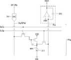
도 3은 도 2에 도시된 표시 픽셀(PIXd)의 구동을 설명하기 위한 도면으로서, 하나의 표시 픽셀(PIXd)과 관련 구성이 도시된다.FIG. 3 is a view for explaining the driving of the display pixel PIXd shown in FIG. 2, and one display pixel PIXd and its related configuration are shown.
참고로, 도 3에 도시된 표시 픽셀(PIXd)은 가장 단순한 형태의 예이며, NMOS로 표현된 트랜지스터는 PMOS로 구성할 수도 있고, Vt 보상 등을 위한 기타의 요소가 구비될 수 있음은 당업자에게는 자명하다.For reference, the display pixel PIXd illustrated in FIG. 3 is an example of the simplest form, and the transistor represented by NMOS may be configured as PMOS, and other elements for Vt compensation may be provided. Self-explanatory
도 3을 참조하면, 상기 다수개의 표시 픽셀(PIXd)들 각각은 대응하는 상기 영상 게이트 라인(GLd)의 활성화에 의하여 선택될 때, 자신의 영상 구동 전압(VDRd)에 따라 발광 억세스되는 유기발광 다이오드(113)를 포함한다.Referring to FIG. 3, when each of the plurality of display pixels PIXd is selected by activation of the corresponding image gate line GLd, an organic light emitting diode that emits light according to its image driving voltage VDRd is accessed. (113).
이때, 상기 다수개의 표시 픽셀(PIXd)들 각각의 상기 영상 구동 전류(IDRd)은 상기 영상 구동 데이터(DATDRd)가 DAC(151)에 의하여 변환된 전류량으로서, 대응하는 상기 영상 데이터 라인(DLd)들 통하여 전송된다.In this case, the image driving current IDRd of each of the plurality of display pixels PIXd is an amount of current in which the image driving data DATDRd is converted by the
한편, 상기 다수개의 표시 픽셀(PIXd)들의 상기 유기발광 다이오드(113)는 '상기 영상 디스플레이 동작'이 반복적으로 수행됨에 따라, 점차 열화된다. 그리고, 상기 다수개의 표시 픽셀(PIXd)들의 상기 유기발광 다이오드(113)는 상기 영상 구동 전류(IDRd)가 클 수록 크게 열화된다.Meanwhile, the organic
다시 도 2를 참조하면, 상기 에이징 디스플레이 블락(200)은 에이징 디스플레이 패널(210), 에이징 게이트 구동회로(230) 및 에이징 데이터 구동 센싱 회로(250)를 구비한다.Referring to FIG. 2 again, the aging
상기 에이징 디스플레이 패널(210)에는, 매트릭스 구조 상에 다수개의 에이징 픽셀(PIXg<1:m>)들이 배열된다. 이때, 상기 다수개의 에이징 픽셀(PIXg<1:m>)들 각각은 발광 억세싱에는 에이징 디스플레이 게이트 라인(GLDg)과 에이징 데이터 라인(DLg)에 의하여 특정된다. 그리고, 상기 다수개의 에이징 픽셀(PIXd<1:m>)들 각각은 상기 '열화 센싱 동작'에서는, 에이징 센싱 게이트 라인(GLSg)과 에이징 센싱 라인(SLg)에 의하여 특정된다.In the aging
상기 에이징 게이트 구동회로(230)는 상기 '영상 디스플레이 동작'에서 상기 에이징 디스플레이 게이트 라인(GLDg)들을 선택적으로 활성화하도록 구동된다. 그리고, 상기 에이징 게이트 구동회로(230)는 상기 '열화 센싱 동작'에서 상기 에이징 센싱 게이트 라인(GLSg)들을 선택적으로 활성화하도록 구동된다.The aging
상기 에이징 데이터 구동 센싱 회로(250)는 상기 '영상 디스플레이 동작'에서, 상기 에이징 데이터 라인(DLg)들을 대응하는 상기 에이징 픽셀(PIXg)들 각각의 상기 에이징 구동 데이터(DATDRg)에 따라 드라이빙하도록 구동된다. 그리고, 상기 에이징 데이터 구동 센싱 회로(250)는 상기 '열화 센싱 동작'에서 상기 에이징 센싱 라인(SLg)들을 통하여, 대응하는 상기 에이징 픽셀(PIXg)들 각각의 상기 열화 센싱값(VSEN)을 독출하도록 구동된다.The aging data driving
이어서, 상기 에이징 픽셀(PIXg)의 구동이 기술된다.Next, the driving of the aging pixel PIXg is described.
도 4는 도 2에 도시된 에이징 픽셀(PIXg)의 구동을 설명하기 위한 도면으로서, 하나의 에이징 픽셀(PIXg)과 관련 구성이 도시된다.FIG. 4 is a view for explaining the driving of the aging pixel PIXg shown in FIG. 2, and one aging pixel PIXg and its related configuration are shown.
도 4를 참조하면, 상기 다수개의 에이징 픽셀(PIXg)들 각각은 대응하는 상기 에이징 디스플레이 게이트 라인(GLDg)의 활성화에 의하여 선택될 때, 자신의 에이징 구동 전압(VDRgd)에 따라 발광 억세스되는 유기발광 다이오드(213)를 포함한다.Referring to FIG. 4, each of the plurality of aging pixels PIXg, when selected by activation of the corresponding aging display gate line GLDg, emits light according to its aging driving voltage VDRgd. And a
이때, 상기 다수개의 에이징 픽셀(PIXg)들 각각의 상기 에이징 구동 전류(IDRg)는 상기 에이징 구동 데이터(DATDRg)가 DAC(251)에 의하여 변환된 전류량으로서, 대응하는 상기 에이징 데이터 라인(DLg)들 통하여 전송된다.In this case, the aging driving current IDRg of each of the plurality of aging pixels PIXg is an amount of current in which the aging driving data DATDRg is converted by the
상기 에이징 픽셀(PIXg)들의 상기 유기발광 다이오드(213)는 '상기 영상 디스플레이 동작'이 반복적으로 수행됨에 따라, 점차 열화된다. 그리고, 상기 에이징 픽셀(PIXg)들의 상기 유기발광 다이오드(213)는 상기 에이징 구동 전류(IDRg)가 클 수록 크게 열화된다.The organic
또한, 상기 다수개의 에이징 픽셀(PIXg)들 각각은 대응하는 상기 에이징 센싱 게이트 라인(GLSg)의 활성화에 의하여 선택될 때, 상기 유기발광 다이오드(213)의 애노드 단자(NAN)의 전압을 대응하는 에이징 센싱 라인(SLg)으로 전송한다.In addition, when each of the plurality of aging pixels PIXg is selected by activation of the corresponding aging sensing gate line GLSg, the aging corresponding to the voltage of the anode terminal NAN of the organic
그리고, 상기 에이징 센싱 라인(SLg)으로 전송된 상기 유기발광 다이오드(213)의 애노드 단자(NAN)의 전압은 상기 에이징 데이터 구동 센싱 회로(250)의 판독 소자(253)을 거쳐 상기 열화 센싱값(VSEN)을 독출된다.In addition, the voltage of the anode terminal NAN of the organic
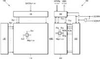
한편, 바람직한 실시예에 따른 본 발명의 유기발광 디스플레이 장치에서는, 상기 에이징 디스플레이 패널(210)의 상면에는 차단 소재(미도시)가 형성된다. 그러므로, 상기 차단 소재(ELBK)에 의하여, 상기 에이징 픽셀(PIXg)들로부터 발광되는 빛의 외부 방출이 차단된다.On the other hand, in the organic light emitting display device of the present invention, a blocking material (not shown) is formed on the upper surface of the aging
그리고, 상기 영상 디스플레이 패널(110)과 상기 에이징 디스플레이 패널(210)은 일체형 패널의 형태로 구현될 수 있다. 이때, 상기 영상 디스플레이 패널(110)과 상기 에이징 디스플레이 패널(210) 사이에는, 버퍼링 영역(ARBF)이 설정된다. 그러므로, 상기 에이징 픽셀(PIXg)들로부터 발광되는 빛의 간섭에 의하여, 상기 영상 디스플레이 패널(110)에 디스플레이되는 이미지의 왜곡 현상이 완화될 수 있다.The
다시 도 1을 참조하면, 상기 열화 보상 제어블락(BKCON)은 구체적으로 에이징 데이터 발생부(300) 및 열화 보상 제어부(400)를 구비한다.Referring back to FIG. 1, the degradation compensation control block BKCON includes an aging
상기 에이징 데이터 발생부(300)는 상기 다수개의 표시 픽셀(PIXd)들 각각의 상기 오리지널 영상 데이터(DATQRd)에 기초하여 상기 다수개의 에이징 픽셀(PIXg)들 각각의 오리지널 에이징 데이터(DATQRg)를 발생한다.The aging
상기 열화 보상 제어부(400)는 상기 열화 상관 정보(IFDE)를 저장한다.The degradation
그리고, 상기 열화 보상 제어부(400)는 상기 열화 상관 정보(IFDE)를 이용하여, 상기 다수개의 표시 픽셀(PIXd)들 각각의 상기 오리지널 영상 데이터(DATQRd)를 열화 보상하여 상기 다수개의 표시 픽셀(PIXd)들 각각의 상기 영상 구동 데이터(DATDRd)로 발생한다.The degradation
또한, 상기 열화 보상 제어부(400)는 상기 열화 상관 정보(IFDE)를 이용하여, 상기 다수개의 에이징 픽셀(PIXg)들 각각의 상기 오리지널 에이징 데이터(DATDRg)를 열화 보상하여 상기 다수개의 에이징 픽셀(PIXg)들 각각의 상기 에이징 구동 데이터(DATDRg)로 발생한다.The deterioration
이때, 상기 오리지널 에이징 데이터(DATQRg)에 대한 열화 보상은, 상기 오리지널 영상 데이터(DATQRd)에 대한 열화 보상과 마찬가지로, 상기 열화 상관 정보(IFDE)에 따라 수행된다.In this case, the deterioration compensation for the original aging data DATQRg is performed according to the deterioration correlation information IFDE, similarly to the deterioration compensation for the original image data DATQRd.
즉, 상기 오리지널 에이징 데이터(DATQRg)에 대한 열화 보상은 자신에 대응하는 상기 에이징 픽셀(PIXg)의 에이징 누적 스트레스 지수(ASTg)에 상응하는 상기 표준 누적 스트레스 지수(RPST)의 상기 열화 확인값(FVA)에 의존되어 수행된다(도 8 참조).That is, the deterioration compensation value for the original aging data DATQRg is the deterioration confirmation value FVA of the standard cumulative stress index RPST corresponding to the aging cumulative stress index ASTg of the aging pixel PIXg corresponding thereto. ), Depending on (see FIG. 8).
계속하여, 상기 에이징 데이터 발생부(300)에서 생성되는 상기 오리지널 에이징 데이터(DATQRg)에 대하여 살펴본다.Subsequently, the original aging data DATQRg generated by the aging
먼저, 특정된 '현재 프레임(예, k번째 프레임)'에서의 상기 다수개의 에이징 픽셀(PIXg)들 각각의 상기 오리지널 에이징 데이터(DATQRg)는 상기 '현재 프레임'에서의 상기 다수개의 표시 픽셀(PIXd)들 각각의 상기 오리지널 영상 데이터(DATQRd) 중에서의 최대 데이터값를 비롯하여, 영상 누적 스트레스 지수(ASTd), 에이징 누적 스트레스 지수(ASTg) 등에 기초하여 결정된다.First, the original aging data DATQRg of each of the plurality of aging pixels PIXg in a specified 'current frame (e.g., k-th frame)' is the plurality of display pixels PIXd in the 'current frame'. ) Is determined based on the image cumulative stress index (ASTd), the aging cumulative stress index (ASTg), and the like, as well as the maximum data value among the original image data DATQRd.
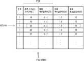
일 예로서, 상기 다수개의 표시 픽셀(PIXd)들 각각의 상기 오리지널 영상 데이터(DATQRd) 중에서의 최대 데이터값이 '255'이고, m은 '9'라 가정하자.As an example, assume that a maximum data value in the original image data DATQRd of each of the plurality of display pixels PIXd is '255' and m is '9'.
이때, 상기 다수개의 에이징 픽셀(PIXg<1:9>)들 각각의 상기 오리지널 에이징 데이터(DATQRg<1:9>)는 (표 1)과 같이 될 수 있다.In this case, the original aging data DATQRg <1: 9> of each of the plurality of aging pixels PIXg <1: 9> may be as shown in Table 1 below.
한편, (표 1)과 같은 방식으로, 상기 오리지널 에이징 데이터(DATQRg)를 생성하는 경우, 상기 '영상 디스플레이 동작'이 반복적으로 진행됨에 따라, 상기 다수개의 표시 픽셀(PIXd)들의 상기 영상 누적 스트레스 지수(ASTd)들 중의 최대값과 상기 다수개의 에이징 픽셀(PIXg)들의 상기 에이징 누적 스트레스 지수(ASTg)들 중의 최대값의 차이는 점점 크게 된다(도 5의 CASE1 참조).Meanwhile, in the same manner as in Table 1, when the original aging data DATQRg is generated, as the 'image display operation' is repeatedly performed, the image cumulative stress index of the plurality of display pixels PIXd. The difference between the maximum value of the ASTds and the maximum value of the aging cumulative stress indexes ASTg of the plurality of aging pixels PIXg becomes larger (see CASE1 of FIG. 5).
다시 기술하자면, 상기 오리지널 영상 데이터(DATQRd)는 특정 표시 픽셀(PIXd)에서 항상 최대값인 255를 가지지 않을 수 있다. 이 경우, 최악 열화 상태를 대비하는 에이징 픽셀(PIXg<1>)과 열화 정도의 차이가 커지게 된다.In other words, the original image data DATQRd may not always have a maximum value of 255 in a specific display pixel PIXd. In this case, the difference between the aging pixel PIXg <1> and the degree of deterioration for the worst deterioration state becomes large.
이에 따라, 상기 다수개의 에이징 픽셀(PIXg)들의 상기 에이징 누적 스트레스 지수(ASTg)들 각각의 간격이 벌어질 수 있고, 본 발명의 효과가 감소될 수 있다.Accordingly, the interval of each of the aging cumulative stress indexes (ASTg) of the plurality of aging pixels (PIXg) can be widened, the effect of the present invention can be reduced.
이를 방지하기 위하여, 보다 바람직한 실시예에서는, 상기 다수개의 에이징 픽셀(PIXg)들 각각의 상기 오리지널 에이징 데이터(DATQRg)는 상기 표시 픽셀(PIXd)의 영상 누적 스트레스 지수들(ASTd) 및 상기 다수개의 에이징 픽셀(PIXg)들의 에이징 누적 스트레스 지수들(ASTg)에 기초한다.In order to prevent this, in the preferred embodiment, the original aging data DATQRg of each of the plurality of aging pixels PIXg may include the image cumulative stress indices ASTd of the display pixel PIXd and the plurality of aging. Based on the aging cumulative stress indices ASTg of the pixels PIXg.
예를 들어, 데이터 셋팅 신호(XDASET)가 활성화되는 경우, 상기 '현재 프레임'에서의 상기 다수개의 에이징 픽셀(PIXg)들 각각의 상기 오리지널 에이징 데이터(DATQRg)는 기본 데이터(예, '0')로 결정된다(CASE2 참조).For example, when the data setting signal XDASET is activated, the original aging data DATQRg of each of the plurality of aging pixels PIXg in the 'current frame' is basic data (eg, '0'). (See CASE2).
그리고, 상기 데이터 셋팅 신호(XDASET)는 다음의 경우에 활성화된다. 즉, '직전 프레임(예, (k-1)번째 프레임)'에서, 상기 다수개의 표시 픽셀(PIXd)들의 상기 영상 누적 스트레스 지수(ASTd)들 중의 최대값(Dmax_d)과 상기 다수개의 에이징 픽셀(PIXg)들의 상기 에이징 누적 스트레스 지수(ASTg)들 중의 최대값의 차이(D_dif)가 허용 범위(D_max)를 초과할 때, 상기 데이터 셋팅 신호(XDASET)는 활성화된다(도 5의 t1 참조).The data setting signal XDASET is activated in the following cases. That is, in the 'previous frame (for example, the (k-1) th frame)', the maximum value Dmax_d of the image cumulative stress indexes ASTMd of the plurality of display pixels PIXd and the plurality of aging pixels ( When the difference D_dif of the maximum value among the aging cumulative stress indexes ASTg of PIXg) exceeds the allowable range D_max, the data setting signal XDASET is activated (see t1 in FIG. 5).
이 경우, 상기 다수개의 에이징 픽셀(PIXg<1:9>)들 각각의 상기 오리지널 에이징 데이터(DATQRg<1:9>)는 (표 2)과 같이 될 수 있다.In this case, the original aging data DATQRg <1: 9> of each of the plurality of aging pixels PIXg <1: 9> may be as shown in Table 2.
상기 (표 2)에서와 같이, 상기 다수개의 에이징 픽셀(PIXg)들 각각의 상기 오리지널 에이징 데이터(DATQRg)는 기본 데이터로 결정됨에 따라, 상기 다수개의 에이징 픽셀(PIXg)들의 상기 에이징 누적 스트레스 지수(ASTg)들 각각의 간격의 벌어짐을 완화할 수 있다.As shown in Table 2, as the original aging data DATQRg of each of the plurality of aging pixels PIXg is determined as basic data, the aging cumulative stress index of the plurality of aging pixels PIXg The spacing of the intervals of each of the ASTg) can be alleviated.
계속하여, 상기 열화 보상 제어부(400)가 구체적으로 기술된다.Subsequently, the degradation
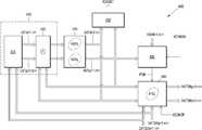
도 6은 도 1의 열화 보상 제어부(400)를 보다 자세히 나타내는 도면이다. 도 6을 참조하면, 상기 열화 보상 제어부(400)는 누적 스트레스 저장 유닛(410), 스트레스 확인 업데이트 유닛(420), 상관 관계 확인 유닛(430), 열화 보상 유닛(440) 및 데이터 셋팅 신호 발생 유닛(450)을 구비한다.FIG. 6 is a diagram illustrating the
상기 누적 스트레스 저장 유닛(410)은 상기 다수개의 표시 픽셀(PIXd)들의 상기 영상 누적 스트레스(ASTd)들과 상기 다수개의 에이징 픽셀들(PIXg)의 상기 에이징 누적 스트레스(ASTg)들을 저장한다.The cumulative
도 7은 도 6의 상기 누적 스트레스 저장 유닛(410)을 보다 자세히 나타내는 도면이다. 도 7을 참조하면, 상기 누적 스트레스 저장 유닛(410)은 휘발성 메모리(411) 및 비휘발성 메모리(413)를 포함하여 구성된다.FIG. 7 illustrates the cumulative
상기 휘발성 메모리(411)는 상기 비휘발성 메모리(413)에 비하여 상대적으로 빠른 동작 속도를 가진다. 그리고, 상기 휘발성 메모리(411)는 상기 다수개의 표시 픽셀(PIXd)들의 상기 영상 누적 스트레스(ASTd)들을 저장하며, 상기 스트레스 확인 업데이트 유닛(420), 상기 상관 관계 확인 유닛(430), 상기 열화 보상 유닛(440) 및 상기 데이터 셋팅 신호 발생 유닛(450)과 상호 통신한다.The
이때, 상기 다수개의 표시 픽셀(PIXd)들 각각의 상기 영상 누적 스트레스 지수(ASTd)는 현재 프레임에서의 대응하는 영상 단위 스트레스 지수(USTd)를 가산하여 업데이트된다. 그리고, 상기 다수개의 에이징 픽셀(PIXg)들 각각의 상기 에이징 누적 스트레스 지수(ASTg)는 현재 프레임에서의 대응하는 상기 에이징 단위 스트레스 지수(USTg)를 가산하여 업데이트된다.In this case, the image cumulative stress index ASTd of each of the plurality of display pixels PIXd is updated by adding a corresponding image unit stress index USTd in the current frame. The aging cumulative stress index ASTg of each of the plurality of aging pixels PIXg is updated by adding the corresponding aging unit stress index USTg in the current frame.
바람직하기로는, 상기 휘발성 메모리(411)는 SRAM이다.Preferably, the
상기 비휘발성 메모리(413)는 상기 휘발성 메모리(411)와 상호 통신한다. 그리고, 상기 비휘발성 메모리(413)는, 전원이 오프된 상태에서도, 상기 영상 누적 스트레스 지수(ASTd)들 및 상기 에이징 누적 스트레스 지수(ASTg)들을 저장한다.The
바람직하기로는, 상기 비휘발성 메모리(413)는 플래시 메모리이다.Preferably, the
한편, 상기 휘발성 메모리(411) 및 상기 비휘발성 메모리(413)에서, 상기 영상 누적 스트레스 지수(ASTd)들 및 상기 에이징 누적 스트레스 지수(ASTg)들은 별도로 구분된 메모리 소자에 저장될 수도 있다.In the
다시 도 6을 참조하면, 상기 스트레스 확인 업데이트 유닛(420)은 상기 다수개의 표시 픽셀(PIXd)들 각각의 상기 영상 단위 스트레스 지수(USTd)들 및 상기 다수개의 에이징 픽셀(PIXg)들 각각의 상기 에이징 단위 스트레스 지수(USTg)들을 확인한다.Referring back to FIG. 6, the stress
이때, 상기 다수개의 표시 픽셀(PIXd)들 각각의 상기 영상 단위 스트레스 지수(USTd)들 각각은 상기 다수개의 표시 픽셀(PIXd)들 각각의 상기 오리지널 영상 데이터(DATQRd)들에 상응한다. 또한, 상기 다수개의 에이징 픽셀(PIXg)들 각각의 상기 에이징 단위 스트레스 지수(USTg)들 각각은 상기 다수개의 에이징 픽셀(PIXg)들 각각의 상기 오리지널 에이징 데이터(DATQRg)들에 상응한다.In this case, each of the image unit stress index USTd of each of the plurality of display pixels PIXd corresponds to the original image data DATQRd of each of the plurality of display pixels PIXd. Further, each of the aging unit stress index USTg of each of the plurality of aging pixels PIXg corresponds to the original aging data DATQRg of each of the plurality of aging pixels PIXg.
그리고, 상기 스트레스 확인 업데이트 유닛(420)은 상기 누적 스트레스 저장 유닛(410)에 저장된 상기 영상 누적 스트레스 지수(ASTd)들 및 상기 에이징 누적 스트레스 지수(ASTg)들을 업데이트하도록 구동된다.The stress
상기 스트레스 확인 업데이트 유닛(420)은 더욱 구체적으로 단위 스트레스 확인 수단(421) 및 스트레스 가산 수단(423)을 구비한다.The stress
상기 단위 스트레스 확인 수단(421)은 상기 다수개의 표시 픽셀(PIXd)들 각각의 상기 오리지널 영상 데이터(DATQRd)를 각각의 상기 영상 단위 스트레스 지수(USTd)로 확인하여 생성한다. 또한, 상기 단위 스트레스 확인 수단(421)은 상기 다수개의 에이징 픽셀(PIXg)들 각각의 상기 오리지널 에이징 데이터(DATQRg)를 각각의 상기 에이징 단위 스트레스 지수(USTg)로 확인하여 생성한다.The unit
상기 스트레스 가산 수단(423)은 상기 다수개의 표시 픽셀(PIXd)들 각자의 상기 영상 단위 스트레스 지수(USTd)를 가산하여 각자의 상기 영상 누적 스트레스 지수(ASTd)를 업데이트한다. 또한, 상기 스트레스 가산 수단(423)은 상기 다수개의 에이징 픽셀(PIXg)들 각자의 상기 에이징 단위 스트레스 지수(USTg)를 가산하여 각자의 상기 에이징 누적 스트레스 지수(ASTg)를 업데이트한다.The stress adding means 423 updates the image cumulative stress index ASTd by adding the image unit stress index USTd of each of the plurality of display pixels PIXd. The stress adding means 423 updates the aging cumulative stress index ASTg by adding the aging unit stress index USTg of each of the plurality of aging pixels PIXg.
계속 도 6을 참조하면, 상기 상관 관계 확인 유닛(430)은 상기 다수개의 에이징 픽셀(PIXg)들 각각의 상기 에이징 누적 스트레스 지수(ASTg)와 상기 열화 센싱값(VSEN)과의 상관 관계를 확인하고, 이에 대한 정보인 센싱 상관 정보(IFSN)를 생성한다.6, the
상기 열화 보상 유닛(440)은 상기 열화 상관 정보(IFDE)를 저장한다. 이때, 상기 열화 상관 정보(IFDE)는 상기 센싱 상관 정보(IFSN)에 의하여 업데이트된다.The
그리고, 상기 열화 보상 유닛(440)은 상기 다수개의 표시 픽셀(PIXd)들 각각의 상기 영상 누적 스트레스 지수(ASTd)에 상응하는 상기 표준 누적 스트레스 지수(PRST)에 대한 상기 열화 확인값(FVA)을 기초로 각자의 오리지널 영상 데이터(DATQRd)를 열화 보상하여 각자의 상기 영상 구동 데이터(DATDRd)를 발생한다.In addition, the
또한, 상기 열화 보상 유닛(440)은 상기 다수개의 에이징 픽셀(PIXg)들 각각의 상기 에이징 누적 스트레스 지수(ASTg)에 상응하는 상기 표준 누적 스트레스 지수(PRST)에 대한 상기 열화 확인값(FVA)을 기초로 각자의 상기 오리지널 에이징 데이터(DATQRd)를 열화 보상하여 각자의 상기 에이징 구동 데이터(DATDRg)로 발생한다.In addition, the
도 8은 도 6의 상기 열화 보상 유닛(440)을 보다 자세히 나타내는 도면이다. 도 8을 참조하면, 상기 상기 열화 보상 유닛(440)은 열화 룩업 테이블(441), 확인값 증폭 수단(443) 및 열화 보상 수단(445)을 구비한다.FIG. 8 is a diagram illustrating the
상기 열화 룩업 테이블(441)은 상기 열화 상관 정보(IFDE)를 저장한다. 이때, 상기 열화 룩업 테이블(441)은 상기 다수개의 표시 픽셀(PIXd)들 각각의 상기 영상 누적 스트레스 지수(ASTd) 및 상기 다수개의 에이징 픽셀(PIXg)들 각각의 상기 에이징 누적 스트레스 지수(ASTg)에 상응하는 상기 열화 확인값(FVA)을 출력한다.The degradation lookup table 441 stores the degradation correlation information IFDE. In this case, the deterioration lookup table 441 is included in the image cumulative stress index ASTd of each of the plurality of display pixels PIXd and the aging cumulative stress index ASTg of each of the plurality of aging pixels PIXg. The corresponding degradation confirmation value FVA is output.
상기 확인값 증폭 수단(443)은 상기 열화 룩업 테이블(441)에서 출력되는 상기 열화 확인값(FVA)을 소정의 증폭율(예, '10')로 증폭하여 증폭 확인값(PVA)으로 발생한다. 이와 같이, 상기 열화 확인값(FVA)이 증폭됨으로써, 상기 열화 보상 수단(445)에서의 열화 보상이 용이해 진다.The confirmation value amplifying means 443 amplifies the degradation confirmation value FVA output from the degradation lookup table 441 to a predetermined amplification rate (eg, '10') and generates the amplification confirmation value PVA. . As described above, the degradation confirmation value FVA is amplified, so that the degradation compensation in the degradation compensation means 445 is facilitated.
상기 열화 보상 수단(445)은 상기 다수개의 표시 픽셀(PIXd)들 각각의 상기 오리지널 영상 데이터(DATQRd)를 열화 보상하여 상기 다수개의 표시 픽셀(PIXd)들 각각의 상기 영상 구동 데이터(DATDRd)로 발생한다. 또한, 상기 열화 보상 수단(445)은 상기 다수개의 에이징 픽셀(PIXg)들 각각의 상기 오리지널 에이징 데이터(DATQRg)를 열화 보상하여 상기 다수개의 에이징 픽셀(PIXg)들 각각의 상기 에이징 구동 데이터(DATDRg)로 발생한다.The deterioration compensating means 445 deteriorates and compensates the original image data DATQRd of each of the plurality of display pixels PIXd to generate the image driving data DATDRd of each of the plurality of display pixels PIXd. do. The deterioration compensating means 445 deteriorates and compensates the original aging data DATQRg of each of the plurality of aging pixels PIXg to deteriorate the aging driving data DATDRg of each of the plurality of aging pixels PIXg. Occurs.
이때, 상기 열화 보상 수단(445)에서의 상기 오리지널 에이징 데이터(DATQRd) 및 상기 오리지널 에이징 데이터(DATQRg)에 대한 열화 보상은 상기 열화 룩업 테이블(441)에서 출력되는 각자의 상기 증폭 확인값(PVA)들에 기초하여 수행된다.In this case, deterioration compensation for the original aging data DATQRd and the original aging data DATQRg in the deterioration compensating means 445 is the amplification confirmation value PVA output from the deterioration lookup table 441. Based on the field.
그리고, 상기 데이터 셋싱 신호 발생유닛(450)은 상기 데이터 셋팅 신호(XDASET)를 발생한다. 이때, 상기 데이터 셋팅 신호(XDASET)가 활성화되는 경우는, 도 5와 관련하여 전술한 바와 같다. 그리고, 이러한 데이터 셋싱 신호 발생유닛(450)의 구현은 당업자라면 용이하므로, 본 명세서에서는, 이에 대한 구체적인 기술은 생략된다.The data setting
계속하여, 상기 표시 픽셀(PIXd<i>)의 오리지널 영상 데이터(DATQRd)에 대한 열화 보상에 대하여 기술된다.Subsequently, deterioration compensation for the original image data DATQRd of the display pixel PIXd <i> is described.
도 9는 도 1의 표시 픽셀(PIXd<i>)의 오리지널 영상 데이터(DATQRd)에 대한 열화 보상의 예를 설명하기 위한 도면이다.FIG. 9 is a diagram for describing an example of deterioration compensation for the original image data DATQRd of the display pixel PIXd <i> of FIG. 1.
예를 들어, 표시 픽셀(PIXd<i>)(여기서, i는 1이상 n 이하의 자연수)의 영상 누적 스트레스 지수(ASTd<i>)가 상기 표준 누적 스트레스 지수(RPST)는 '20'에 해당하면, 상기 표시 픽셀(PIXd<i>)의 열화 확인값(FVA)은 0.13V로 확인된다. 그리고, 상기 증폭 확인값(PVA)은 '1.3V'이다.For example, the image cumulative stress index ASTd <i> of the display pixel PIXd <i> (where i is a natural number greater than or equal to 1 and less than n) corresponds to the standard cumulative stress index RPST of '20'. Then, the degradation confirmation value FVA of the display pixel PIXd <i> is confirmed to be 0.13V. The amplification confirmation value PVA is '1.3 V'.
이때, 상기 표시 픽셀(PIXd<i>)에 대한 열화 보상값(CVA)는 '13'으로 확인된다.In this case, the degradation compensation value CVA for the display pixel PIXd <i> is identified as '13'.
이 경우에, 상기 표시 픽셀(PIXd<i>)의 오리지널 영상 데이터(DATQRd)의 데이터값이 '142'라면, 상기 영상 구동 데이터(DATDRd)는 '155=(142+13)'으로 결정된다.In this case, if the data value of the original image data DATQRd of the display pixel PIXd <i> is '142', the image driving data DATDRd is determined to be '155 = (142 + 13)'.
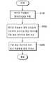
도 10은 본 발명의 유기발광 디스플레이 장치의 구동을 설명하기 위한 순서도이다. 도 10을 참조하여, 본 발명의 유기발광 디스플레이 장치의 구동을 정리하면, 다음과 같다.10 is a flowchart illustrating driving of an organic light emitting display device of the present invention. Referring to FIG. 10, driving of the organic light emitting display device according to the present invention is summarized as follows.
먼저, S100 단계에서, 열화 센싱 동작이 진행됨에 따라, 상기 에이징 픽셀(PIXg)들의 열화 센싱값(VSEN)이 추출된다.First, in operation S100, as the degradation sensing operation is performed, the degradation sensing value VSEN of the aging pixels PIXg is extracted.
S200 단계에서, 추출된 상기 에이징 픽셀(PIXg)들의 열화 센싱값(VSEN)에 기초하여, 상기 표시 픽셀(PIXd)들의 오리지널 영상 데이터(DATQRd)가 영상 구동 데이터(DATDRd)로 생성된다.In operation S200, the original image data DATQRd of the display pixels PIXd is generated as the image driving data DATDRd based on the extracted sensing value VSEN of the aging pixels PIXg.
그리고, S300 단계에서, 영상 디스플레이 동작이 진행됨에 따라, 상기 표시 픽셀(PIXd)들이 상기 영상 구동 데이터(DATDRd)에 따라 발광 억세싱된다.In operation S300, as the image display operation is performed, the display pixels PIXd may emit light according to the image driving data DATDRd.
이상과 같이 실시예들이 비록 한정된 실시예와 도면에 의해 설명되었으나, 해당 기술분야에서 통상의 지식을 가진 자라면 상기의 기재로부터 다양한 수정 및 변형이 가능하다.Although the embodiments have been described by the limited embodiments and the drawings as described above, various modifications and variations are possible to those skilled in the art from the above description.
예를 들어, 본 명세서에서는, 각종의 ~데이터, ~ 스트레스 지수 등에 대해, 표시 픽셀들에 관한 흐름과 에이징 픽셀들에 관한 흐름이 별개로 진행되는 실시예가 도시되고 기술되었다.For example, in the present specification, an embodiment in which the flow regarding the display pixels and the flow regarding the aging pixels proceeds separately for various data, stress index, and the like is shown and described.
그러나, 본 발명의 기술적 사상은 상기 각종의 ~데이터, ~ 스트레스 지수 등이 하나의 흐름 즉, 표시 픽셀들에 관한 흐름에 이어서 에이징 픽셀들에 관한 흐름이 시리얼로 진행되는 실시예에 의해서 구현될 수 있음은 당업자에게는 자명하다.However, the technical idea of the present invention may be implemented by an embodiment in which the various data, the stress index, and the like flow in one serial, that is, flows related to aging pixels, followed by flows related to aging pixels. It is apparent to those skilled in the art.
또한, 본 명세서에서는, 열화 보상 방법과 관련하여, 열화 정도에 따른 열화 보상값(CVA)을 생성하고, 생성된 열화 보상값(CVA)을 오리지널 영상 데이터(DATQRd)에 더하여 영상 구동 데이터(DATDRd)로 생성하는 실시예가 도시되고 기술되었다.In addition, in the present specification, in relation to the degradation compensation method, the degradation compensation value CVA according to the degree of degradation is generated, and the generated degradation compensation value CVA is added to the original image data DATQRd to drive the image driving data DATDRd. An embodiment for generating a furnace has been shown and described.
그러나, 본 발명의 기술적 사상은 열화 보상 방법과 관련하여, 열화 정도에 따른 증폭 비율을 생성하고, 생성된 증폭 비율을 오리지널 영상 데이터(DATQRd)에 곱하여 영상 구동 데이터(DATDRd)로 생성하는 실시예에 의해서도 구현될 수 있음은 당업자에게는 자명하다.However, the technical concept of the present invention relates to an embodiment of generating an amplification ratio according to the degree of deterioration and multiplying the generated amplification ratio by the original image data DATQRd to generate the image driving data DATDRd. It will be apparent to those skilled in the art that the present invention may also be implemented by.
따라서, 본 발명의 진정한 기술적 보호 범위는 첨부된 등록청구범위의 기술적 사상에 의해 정해져야 할 것이다.Therefore, the true technical protection scope of the present invention will be defined by the technical spirit of the appended claims.
Claims (12)
Translated fromKorean영상 디스플레이 동작에서, 하나의 프레임 동안에 하나의 영상을 디스플레이하도록 구동되는 다수개의 표시 픽셀들이 배열되는 영상 디스플레이 블락으로서, 상기 다수개의 표시 픽셀들 각각은 상기 영상 디스플레이 동작에서 각자의 영상 구동 데이터에 따라 발광 억세싱되는 상기 영상 디스플레이 블락;
다수개의 에이징 픽셀들이 배열되는 에이징 디스플레이 블락으로서, 상기 다수개의 에이징 픽셀들 각각은 상기 영상 디스플레이 블락의 상기 다수개의 표시 픽셀들의 열화 정도를 반영하도록 열화되며, 열화 센싱 동작에서 자신의 열화 정도를 반영하는 전기적 성분인 각자의 열화 센싱값을 독출하도록 구동되는 상기 에이징 디스플레이 블락; 및
다수개의 표준 누적 스트레스 지수들 각각에 대한 열화 확인값을 나타내는 열화 상관 정보를 저장하되, 상기 열화 상관 정보는 상기 다수개의 에이징 픽셀들 각각의 상기 열화 센싱값에 의존되어 업데이트되는 열화 보상 제어블락으로서, 상기 다수개의 표시 픽셀들 각자의 오리지널 영상 데이터를 상기 열화 상관 정보에 따라 열화 보상하여 각자의 상기 영상 구동 데이터로 제공하는 상기 열화 보상 제어블락을 구비하며,
상기 오리지널 영상 데이터에 대한 열화 보상은
자신에 대응하는 상기 표시 픽셀의 영상 누적 스트레스 지수에 상응하는 상기 표준 누적 스트레스 지수의 상기 열화 확인값에 의존되어 수행되며,
상기 영상 누적 스트레스 지수는
자신에 대응하는 상기 표시 픽셀의 누적 스트레스를 나타내며,
상기 다수개의 에이징 픽셀들 각각은
상기 열화 센싱 동작이 미수행되는 상기 영상 디스플레이 동작에서 각자의 에이징 구동 데이터에 따라 발광 억세싱되며,
상기 열화 보상 제어 블락은
상기 다수개의 표시 픽셀들 각각의 상기 오리지널 영상 데이터에 기초하여 상기 다수개의 에이징 픽셀들 각각의 오리지널 에이징 데이터를 발생하는 에이징 데이터 발생부; 및
상기 열화 상관 정보를 저장하는 열화 보상 제어부로서, 상기 열화 상관 정보를 이용하여 상기 다수개의 표시 픽셀들 각각의 상기 오리지널 영상 데이터를 열화 보상하여 상기 다수개의 표시 픽셀들 각각의 상기 영상 구동 데이터로 발생하고, 상기 다수개의 에이징 픽셀들 각각의 상기 오리지널 에이징 데이터를 열화 보상하여 상기 다수개의 에이징 픽셀들 각각의 상기 에이징 구동 데이터로 발생하는 열화 보상 제어부를 구비하며,
상기 오리지널 에이징 데이터에 대한 열화 보상은
자신에 대응하는 상기 에이징 픽셀의 에이징 누적 스트레스 지수에 상응하는 상기 표준 누적 스트레스 지수의 상기 열화 확인값에 의존되어 수행되며,
상기 에이징 누적 스트레스 지수는
자신에 대응하는 상기 에이징 픽셀의 누적 스트레스를 나타내는 것을 특징으로 하는 유기발광 디스플레이 장치.
In the organic light emitting display device having a degradation compensation function,
In an image display operation, an image display block in which a plurality of display pixels driven to display one image is arranged during one frame, wherein each of the plurality of display pixels emits light according to respective image driving data in the image display operation. The image display block being accessed;
An aging display block in which a plurality of aging pixels are arranged, each of the plurality of aging pixels deteriorated to reflect a deterioration degree of the plurality of display pixels of the image display block, and reflecting its deterioration degree in a deterioration sensing operation. An aging display block driven to read respective degradation sensing values which are electrical components; And
A deterioration correlation control block which stores deterioration correlation information representing a deterioration confirmation value for each of a plurality of standard cumulative stress indices, wherein the deterioration correlation information is updated depending on the deterioration sensing value of each of the plurality of aging pixels. And a deterioration compensation control block for deteriorating and compensating original image data of each of the plurality of display pixels according to the deterioration correlation information and providing the deterioration compensation data to the respective image driving data.
Deterioration compensation for the original image data
Is performed depending on the deterioration confirmation value of the standard cumulative stress index corresponding to the image cumulative stress index of the display pixel corresponding to the self,
The image cumulative stress index is
Represents a cumulative stress of the display pixel corresponding to itself,
Each of the plurality of aging pixels
In the image display operation in which the deterioration sensing operation is not performed, light emission is accessed according to respective aging driving data.
The deterioration compensation control block
An aging data generator for generating original aging data of each of the plurality of aging pixels based on the original image data of each of the plurality of display pixels; And
A deterioration compensation control unit configured to store the deterioration correlation information, wherein the deterioration compensation of the original image data of each of the plurality of display pixels is performed as the image driving data of each of the plurality of display pixels using the deterioration correlation information; And a degradation compensation controller configured to degrade and compensate the original aging data of each of the plurality of aging pixels to generate the aging driving data of each of the plurality of aging pixels.
Deterioration compensation for the original aging data
Is performed depending on the deterioration confirmation value of the standard cumulative stress index corresponding to the aging cumulative stress index of the aging pixel corresponding thereto,
The aging cumulative stress index is
And a cumulative stress of the aging pixel corresponding to the organic light emitting display device.
상기 현재 프레임에서의 상기 다수개의 표시 픽셀들 각각의 상기 오리지널 영상 데이터 중에서의 최대 데이터값에 기초하여 결정되는 것을 특징으로 하는 유기발광 디스플레이 장치.
The method of claim 1, wherein the original aging data of each of the plurality of aging pixels in the current frame is
And an organic light emitting display device configured to be determined based on a maximum data value of the original image data of each of the plurality of display pixels in the current frame.
상기 다수개의 표시 픽셀들의 상기 영상 누적 스트레스 지수들과 상기 다수개의 에이징 픽셀들의 상기 에이징 누적 스트레스 지수들을 저장하는 누적 스트레스 저장 유닛;
상기 다수개의 표시 픽셀들 각각의 영상 단위 스트레스 지수들 및 상기 다수개의 에이징 픽셀들 각각의 에이징 단위 스트레스 지수들을 확인하여, 상기 누적 스트레스 저장 유닛에 저장된 상기 영상 누적 스트레스 지수들 및 상기 에이징 누적 스트레스 지수들을 업데이트하도록 구동되는 스트레스 확인 업데이트 유닛으로서, 상기 다수개의 표시 픽셀들 각각의 상기 영상 단위 스트레스 지수들 각각은 상기 다수개의 표시 픽셀들 각각의 상기 오리지널 영상 데이터들에 상응하며, 상기 다수개의 에이징 픽셀들 각각의 상기 에이징 단위 스트레스 지수들 각각은 상기 다수개의 에이징 픽셀들 각각의 상기 오리지널 에이징 데이터들에 상응하는 상기 스트레스 확인 업데이트 유닛;
상기 다수개의 에이징 픽셀들 각각의 상기 에이징 누적 스트레스 지수와 상기 열화 센싱값과의 상관 관계를 확인하여 센싱 상관 정보를 생성하는 상관 관계 확인 유닛; 및
상기 열화 상관 정보를 저장하는 열화 보상 유닛으로서, 상기 다수개의 표시 픽셀들 각각의 상기 영상 누적 스트레스 지수에 상응하는 상기 표준 누적 스트레스 지수에 대한 상기 열화 확인값을 기초로 각자의 상기 오리지널 영상 데이터를 열화 보상하여 각자의 상기 영상 구동 데이터로 발생하고, 상기 다수개의 에이징 픽셀들 각각의 상기 에이징 누적 스트레스 지수에 상응하는 상기 표준 누적 스트레스 지수에 대한 상기 열화 확인값을 기초로 각자의 상기 오리지널 에이징 데이터를 열화 보상하여 각자의 상기 에이징 구동 데이터로 발생하는 상기 열화 보상 유닛을 구비하며,
상기 열화 보상 유닛의 상기 열화 상관 정보는
상기 센싱 상관 정보에 의하여 업데이트되는 것을 특징으로 하는 유기발광 디스플레이 장치.
The deterioration compensation controller of claim 1, wherein
A cumulative stress storage unit for storing the image cumulative stress indices of the plurality of display pixels and the aging cumulative stress indices of the plurality of aging pixels;
Identifying image unit stress indices of each of the plurality of display pixels and aging unit stress indices of each of the plurality of aging pixels to determine the image cumulative stress indices and the aging cumulative stress indices stored in the cumulative stress storage unit. A stress confirmation updating unit driven to update, each of the image unit stress indices of each of the plurality of display pixels corresponding to the original image data of each of the plurality of display pixels, wherein each of the plurality of aging pixels Each of the aging unit stress indices of the stress confirmation updating unit corresponding to the original aging data of each of the plurality of aging pixels;
A correlation checking unit configured to check the correlation between the aging cumulative stress index of each of the plurality of aging pixels and the degradation sensing value to generate sensing correlation information; And
A deterioration compensation unit for storing the deterioration correlation information, wherein the deterioration compensation unit deteriorates respective original image data based on the deterioration confirmation value for the standard cumulative stress index corresponding to the image cumulative stress index of each of the plurality of display pixels. Compensating to generate the respective image driving data, and degrading the respective original aging data based on the deterioration confirmation value for the standard cumulative stress index corresponding to the aging cumulative stress index of each of the plurality of aging pixels. And the deterioration compensation unit for compensating to generate the respective aging drive data.
The deterioration correlation information of the deterioration compensation unit is
The organic light emitting display device, characterized in that updated by the sensing correlation information.
상기 다수개의 표시 픽셀들의 상기 영상 누적 스트레스 지수들과 상기 다수개의 에이징 픽셀들의 상기 에이징 누적 스트레스 지수들을 저장하며, 상기 스트레스 확인 업데이트 유닛, 상기 상관 관계 확인 유닛 및 상기 열화 보상 유닛과 상호 통신하는 휘발성 메모리로서, 상기 다수개의 표시 픽셀들 각각의 상기 영상 누적 스트레스 지수는 대응하는 상기 영상 단위 스트레스 지수에 의존하여 업데이트되며, 상기 다수개의 에이징 픽셀들 각각의 상기 에이징 누적 스트레스 지수는 대응하는 상기 에이징 단위 스트레스 지수에 의존하여 업데이트되는 상기 휘발성 메모리; 및
전원이 오프된 상태에서도 상기 영상 누적 스트레스 지수들 및 상기 에이징 누적 스트레스 지수들을 저장하는 비휘발성 메모리로서, 상기 휘발성 메모리와 상호 통신하는 상기 비휘발성 메모리를 구비하는 것을 특징으로 하는 유기발광 디스플레이 장치.
The method of claim 4, wherein the cumulative stress storage unit
A volatile memory for storing the image cumulative stress indices of the plurality of display pixels and the aging cumulative stress indices of the plurality of aging pixels, the volatile memory being in communication with the stress confirmation updating unit, the correlation checking unit and the degradation compensation unit Wherein the image cumulative stress index of each of the plurality of display pixels is updated depending on the corresponding image unit stress index, and the aging cumulative stress index of each of the plurality of aging pixels is corresponding to the aging unit stress index. The volatile memory updated in dependence on the volatile memory; And
And a nonvolatile memory configured to store the image cumulative stress indexes and the aging cumulative stress indexes even when the power is turned off, the nonvolatile memory communicating with the volatile memory.
상기 다수개의 표시 픽셀들 각각의 상기 오리지널 영상 데이터를 각각의 상기 영상 단위 스트레스 지수로 확인하여 생성하고, 상기 다수개의 에이징 픽셀들 각각의 상기 오리지널 에이징 데이터를 각각의 상기 에이징 단위 스트레스 지수로 확인하여 생성하는 단위 스트레스 확인 수단; 및
상기 다수개의 표시 픽셀들 각자의 상기 영상 단위 스트레스 지수를 가산하여 각자의 상기 영상 누적 스트레스 지수를 업데이트하며, 상기 다수개의 에이징 픽셀들 각자의 상기 에이징 단위 스트레스 지수를 가산하여 각자의 상기 에이징 누적 스트레스 지수를 업데이트하는 스트레스 가산 수단을 구비하는 것을 특징으로 하는 유기발광 디스플레이 장치.
The method of claim 4, wherein the stress check update unit
The original image data of each of the plurality of display pixels is generated by checking the respective image unit stress index, and the original aging data of each of the plurality of aging pixels is generated by each of the aging unit stress index. Unit stress checking means; And
Add the image unit stress index of each of the plurality of display pixels to update the respective image cumulative stress index, and add the aging unit stress index of each of the plurality of aging pixels to add the respective aging cumulative stress index The organic light emitting display device comprising a stress adding means for updating the.
상기 열화 상관 정보를 저장하며, 상기 다수개의 표시 픽셀들 각각의 상기 영상 누적 스트레스 지수 및 상기 다수개의 에이징 픽셀들 각각의 상기 에이징 누적 스트레스 지수에 상응하는 상기 열화 확인값을 출력하는 열화 룩업 테이블;
상기 열화 룩업 테이블에서 출력되는 상기 열화 확인값을 증폭하여 증폭 확인값으로 발생하는 확인값 증폭 수단; 및
상기 다수개의 표시 픽셀들 각각의 상기 오리지널 영상 데이터를 열화 보상하여 상기 다수개의 표시 픽셀들 각각의 상기 영상 구동 데이터로 발생하고, 상기 다수개의 에이징 픽셀들 각각의 상기 오리지널 에이징 데이터를 열화 보상하여 상기 다수개의 에이징 픽셀들 각각의 상기 에이징 구동 데이터로 발생하는 열화 보상 수단을 구비하며,
상기 열화 보상 수단에서의 상기 오리지널 영상 데이터 및 상기 오리지널 에이징 데이터에 대한 열화 보상은
상기 확인 증폭 수단에서 출력되는 각자의 상기 증폭 확인값들에 기초하여 수행되는 것을 특징으로 하는 유기발광 디스플레이 장치.
The deterioration compensation unit of claim 4, wherein
A deterioration lookup table for storing the deterioration correlation information and outputting the deterioration confirmation value corresponding to the image cumulative stress index of each of the plurality of display pixels and the aging cumulative stress index of each of the plurality of aging pixels;
Confirmation value amplification means for amplifying the degradation confirmation value output from the degradation lookup table and generating an amplification confirmation value; And
Degradation compensation of the original image data of each of the plurality of display pixels is generated as the image driving data of each of the plurality of display pixels, and degradation compensation of the original aging data of each of the plurality of aging pixels is performed. Deterioration compensation means generated by the aging drive data of each of the aging pixels,
Deterioration compensation for the original image data and the original aging data in the deterioration compensation means
And the amplification confirmation values output from the confirmation amplification means.
직전 프레임에서, 상기 영상 누적 스트레스 지수들 및 상기 에이징 누적 스트레스 지수들에 기초하여 활성화되는 데이터 셋팅 신호를 발생하는 데이터 셋팅 신호 발생유닛을 더 구비하며,
상기 에이징 데이터 발생부는
상기 데이터 셋팅 신호의 활성화에 따라, 상기 영상 누적 스트레스 지수들 및 상기 에이징 누적 스트레스 지수들에 기초하여, 현재 프레임에서의 상기 다수개의 에이징 픽셀들 각각의 오리지널 에이징 데이터를 결정하도록 구동되는 것을 특징으로 하는 특징으로 하는 유기발광 디스플레이 장치.
The deterioration compensation controller of claim 4, wherein
And a data setting signal generating unit for generating a data setting signal that is activated based on the image cumulative stress indexes and the aging cumulative stress indexes in a previous frame,
The aging data generation unit
And in response to the activation of the data setting signal, driving to determine original aging data of each of the plurality of aging pixels in a current frame based on the image cumulative stress indices and the aging cumulative stress indices. An organic light emitting display device.
영상 디스플레이 동작에서, 하나의 프레임 동안에 하나의 영상을 디스플레이하도록 구동되는 다수개의 표시 픽셀들이 배열되는 영상 디스플레이 블락으로서, 상기 다수개의 표시 픽셀들 각각은 상기 영상 디스플레이 동작에서 각자의 영상 구동 데이터에 따라 발광 억세싱되는 상기 영상 디스플레이 블락;
다수개의 에이징 픽셀들이 배열되는 에이징 디스플레이 블락으로서, 상기 다수개의 에이징 픽셀들 각각은 상기 영상 디스플레이 블락의 상기 다수개의 표시 픽셀들의 열화 정도를 반영하도록 열화되며, 열화 센싱 동작에서 자신의 열화 정도를 반영하는 전기적 성분인 각자의 열화 센싱값을 독출하도록 구동되는 상기 에이징 디스플레이 블락; 및
다수개의 표준 누적 스트레스 지수들 각각에 대한 열화 확인값을 나타내는 열화 상관 정보를 저장하되, 상기 열화 상관 정보는 상기 다수개의 에이징 픽셀들 각각의 상기 열화 센싱값에 의존되어 업데이트되는 열화 보상 제어블락으로서, 상기 다수개의 표시 픽셀들 각자의 오리지널 영상 데이터를 상기 열화 상관 정보에 따라 열화 보상하여 각자의 상기 영상 구동 데이터로 제공하는 상기 열화 보상 제어블락을 구비하며,
상기 오리지널 영상 데이터에 대한 열화 보상은
자신에 대응하는 상기 표시 픽셀의 영상 누적 스트레스 지수에 상응하는 상기 표준 누적 스트레스 지수의 상기 열화 확인값에 의존되어 수행되며,
상기 영상 누적 스트레스 지수는
자신에 대응하는 상기 표시 픽셀의 누적 스트레스를 나타내며,
상기 다수개의 에이징 픽셀들 각각은
상기 열화 센싱 동작이 미수행되는 상기 영상 디스플레이 동작에서 각자의 에이징 구동 데이터에 따라 발광 억세싱되며,
상기 에이징 디스플레이 블락의 상기 다수개의 에이징 픽셀들 각각은
상기 영상 디스플레이 동작에서 각자의 에이징 구동 데이터에 따라 발광하며,
상기 다수개의 에이징 픽셀들 각각의 상기 에이징 구동 데이터는
상기 다수개의 표시 픽셀들 각각의 상기 오리지널 영상 데이터에 기초되어 결정되는 것을 특징으로 하는 유기발광 디스플레이 장치.
In the organic light emitting display device having a degradation compensation function,
In an image display operation, an image display block in which a plurality of display pixels driven to display one image is arranged during one frame, wherein each of the plurality of display pixels emits light according to respective image driving data in the image display operation. The image display block being accessed;
An aging display block in which a plurality of aging pixels are arranged, each of the plurality of aging pixels deteriorated to reflect a deterioration degree of the plurality of display pixels of the image display block, and reflecting its deterioration degree in a deterioration sensing operation. An aging display block driven to read respective degradation sensing values which are electrical components; And
A deterioration correlation control block indicating deterioration confirmation value for each of a plurality of standard cumulative stress indices, wherein the deterioration correlation information is updated according to the deterioration sensing value of each of the plurality of aging pixels; And a deterioration compensation control block for deteriorating and compensating original image data of each of the plurality of display pixels according to the deterioration correlation information and providing the deterioration compensation data to the respective image driving data.
Deterioration compensation for the original image data
Is performed depending on the deterioration confirmation value of the standard cumulative stress index corresponding to the image cumulative stress index of the display pixel corresponding to the self,
The image cumulative stress index is
Represents a cumulative stress of the display pixel corresponding to itself,
Each of the plurality of aging pixels
In the image display operation in which the deterioration sensing operation is not performed, light emission is accessed according to respective aging driving data.
Each of the plurality of aging pixels of the aging display block
In the image display operation to emit light according to the respective aging drive data,
The aging drive data of each of the plurality of aging pixels is
And an organic light emitting display device configured to be determined based on the original image data of each of the plurality of display pixels.
상기 다수개의 에이징 픽셀들 각각의 상기 에이징 구동 데이터는
상기 다수개의 에이징 픽셀들 각각의 오리지널 에이징 데이터를 열화 보상하여 생성되되,
상기 다수개의 에이징 픽셀들 각각의 상기 오리지널 에이징 데이터는
상기 다수개의 표시 픽셀들 각각의 상기 오리지널 영상 데이터에 기초하여 발생되는 것을 특징으로 하는 유기발광 디스플레이 장치.
The method of claim 9,
The aging drive data of each of the plurality of aging pixels is
Generated by deteriorating and compensating original aging data of each of the plurality of aging pixels,
The original aging data of each of the plurality of aging pixels is
And an organic light emitting display device which is generated based on the original image data of each of the plurality of display pixels.
상기 다수개의 에이징 픽셀들 각각의 상기 오리지널 에이징 데이터는
상기 다수개의 표시 픽셀들 각각의 상기 영상 누적 스트레스 지수에 기초하여 발생되는 것을 특징으로 하는 유기발광 디스플레이 장치.
The method of claim 10,
The original aging data of each of the plurality of aging pixels is
And an organic light emitting display device which is generated based on the image cumulative stress index of each of the plurality of display pixels.
상기 다수개의 에이징 픽셀들의 상기 열화 센싱값에 의존되어 수행되는 것을 특징으로 하는 유기발광 디스플레이 장치.
11. The method of claim 10, wherein the degradation compensation for the original aging data is
And an organic light emitting display device according to the deterioration sensing value of the plurality of aging pixels.
Priority Applications (3)
| Application Number | Priority Date | Filing Date | Title |
|---|---|---|---|
| KR1020190051133AKR102085516B1 (en) | 2019-05-01 | 2019-05-01 | Organic light emmiting display having effective degradation compensating structure |
| US16/827,023US10950185B2 (en) | 2019-05-01 | 2020-03-23 | Organic light-emitting display device having degradation compensation |
| CN202010325273.9ACN111883051B (en) | 2019-05-01 | 2020-04-23 | Organic light emitting display device with degradation compensation |
Applications Claiming Priority (1)
| Application Number | Priority Date | Filing Date | Title |
|---|---|---|---|
| KR1020190051133AKR102085516B1 (en) | 2019-05-01 | 2019-05-01 | Organic light emmiting display having effective degradation compensating structure |
Publications (1)
| Publication Number | Publication Date |
|---|---|
| KR102085516B1true KR102085516B1 (en) | 2020-03-05 |
Family
ID=69804014
Family Applications (1)
| Application Number | Title | Priority Date | Filing Date |
|---|---|---|---|
| KR1020190051133AActiveKR102085516B1 (en) | 2019-05-01 | 2019-05-01 | Organic light emmiting display having effective degradation compensating structure |
Country Status (3)
| Country | Link |
|---|---|
| US (1) | US10950185B2 (en) |
| KR (1) | KR102085516B1 (en) |
| CN (1) | CN111883051B (en) |
Families Citing this family (5)
| Publication number | Priority date | Publication date | Assignee | Title |
|---|---|---|---|---|
| KR20220030333A (en)* | 2020-08-27 | 2022-03-11 | 삼성디스플레이 주식회사 | Display device and driving method of display device |
| US11626047B1 (en)* | 2020-09-25 | 2023-04-11 | Apple Inc. | Reference array current sensing |
| KR20230064704A (en)* | 2021-11-03 | 2023-05-11 | 삼성디스플레이 주식회사 | Display device and method for compensating for degradation thereof |
| KR20230167203A (en)* | 2022-05-30 | 2023-12-08 | 삼성디스플레이 주식회사 | Display system and method of driving the same |
| US12125436B1 (en) | 2023-05-30 | 2024-10-22 | Apple Inc. | Pixel drive circuitry burn-in compensation systems and methods |
Citations (4)
| Publication number | Priority date | Publication date | Assignee | Title |
|---|---|---|---|---|
| KR20110031096A (en)* | 2009-09-18 | 2011-03-24 | 소니 주식회사 | Display device |
| KR20130067092A (en) | 2011-12-13 | 2013-06-21 | 엘지디스플레이 주식회사 | Organic light emitting display and compensation method of degradation thereof |
| KR20170036938A (en) | 2015-09-24 | 2017-04-04 | 삼성디스플레이 주식회사 | Degradation compensation device and display device having the same |
| KR20170136028A (en) | 2016-05-30 | 2017-12-11 | 엘지디스플레이 주식회사 | Organic light-emitting diode display and method for compensating degradation of luminous element |
Family Cites Families (12)
| Publication number | Priority date | Publication date | Assignee | Title |
|---|---|---|---|---|
| KR100902238B1 (en)* | 2008-01-18 | 2009-06-11 | 삼성모바일디스플레이주식회사 | Organic light emitting display device and driving method thereof |
| US10176736B2 (en)* | 2010-02-04 | 2019-01-08 | Ignis Innovation Inc. | System and methods for extracting correlation curves for an organic light emitting device |
| KR101470688B1 (en)* | 2011-12-08 | 2014-12-08 | 엘지디스플레이 주식회사 | Organic Light Emitting Display And Compensation Method Of Degradation Thereof |
| KR101960795B1 (en)* | 2012-12-17 | 2019-03-21 | 엘지디스플레이 주식회사 | Organic light emitting display device and method for driving thereof |
| KR101997875B1 (en)* | 2013-01-24 | 2019-07-12 | 삼성디스플레이 주식회사 | Organic Light Emitting Display Device and Driving Method Thereof |
| KR20140133189A (en)* | 2013-05-10 | 2014-11-19 | 삼성디스플레이 주식회사 | Pixel of an organic light emitting display device and organic light emitting display device |
| CN112002285B (en)* | 2014-06-25 | 2021-10-29 | 伊格尼斯创新公司 | Method for determining and compensating efficiency degradation of organic light emitting device |
| KR102336090B1 (en)* | 2014-12-15 | 2021-12-07 | 삼성디스플레이 주식회사 | Orgainic light emitting display and driving method for the same |
| KR102236561B1 (en)* | 2014-12-31 | 2021-04-07 | 삼성디스플레이 주식회사 | Display device, appratus for compensating degradation and method thereof |
| KR102406206B1 (en)* | 2015-01-20 | 2022-06-09 | 삼성디스플레이 주식회사 | Organic light emitting display device and method of driving the same |
| KR102522478B1 (en)* | 2016-11-25 | 2023-04-17 | 엘지디스플레이 주식회사 | Organic light emitting display device and method for drving the same |
| KR102617215B1 (en)* | 2017-09-21 | 2023-12-27 | 애플 인크. | Oled voltage driver with current-voltage compensation |
- 2019
- 2019-05-01KRKR1020190051133Apatent/KR102085516B1/enactiveActive
- 2020
- 2020-03-23USUS16/827,023patent/US10950185B2/enactiveActive
- 2020-04-23CNCN202010325273.9Apatent/CN111883051B/enactiveActive
Patent Citations (4)
| Publication number | Priority date | Publication date | Assignee | Title |
|---|---|---|---|---|
| KR20110031096A (en)* | 2009-09-18 | 2011-03-24 | 소니 주식회사 | Display device |
| KR20130067092A (en) | 2011-12-13 | 2013-06-21 | 엘지디스플레이 주식회사 | Organic light emitting display and compensation method of degradation thereof |
| KR20170036938A (en) | 2015-09-24 | 2017-04-04 | 삼성디스플레이 주식회사 | Degradation compensation device and display device having the same |
| KR20170136028A (en) | 2016-05-30 | 2017-12-11 | 엘지디스플레이 주식회사 | Organic light-emitting diode display and method for compensating degradation of luminous element |
Also Published As
| Publication number | Publication date |
|---|---|
| CN111883051A (en) | 2020-11-03 |
| US10950185B2 (en) | 2021-03-16 |
| US20200349894A1 (en) | 2020-11-05 |
| CN111883051B (en) | 2022-08-02 |
Similar Documents
| Publication | Publication Date | Title |
|---|---|---|
| KR102085516B1 (en) | Organic light emmiting display having effective degradation compensating structure | |
| KR102617392B1 (en) | Degradation compensation device and display device including the same | |
| KR102411075B1 (en) | Pixel and organic light emitting display device having the same | |
| US11322075B2 (en) | Optical compensation system and optical compensation method of display device | |
| US9111489B2 (en) | Organic light emitting display device and method of driving the same | |
| JP5535627B2 (en) | Method and display for compensating for pixel luminance degradation | |
| CN113853645B (en) | Display device and driving method thereof | |
| KR102784308B1 (en) | Display device and driving method thereof | |
| KR20170051630A (en) | Luminance control device and display device including the same | |
| JP5589392B2 (en) | Signal processing device, display device, electronic device, signal processing method and program | |
| US20110148847A1 (en) | Method of driving display apparatus | |
| JP2008046617A (en) | System and method for reducing mura deffect | |
| KR102067228B1 (en) | Organic lighting emitting device and method for compensating degradation thereof | |
| KR100707637B1 (en) | Light emitting display device and control method thereof | |
| KR20210158566A (en) | Display device, method for compensation data signal of display device, and a method of generating a compensation model based on a deep learning of a display device | |
| JP2014071450A (en) | Organic light emitting display and method of erasing afterimage thereof | |
| KR102369759B1 (en) | Display apparaus, display method, and program | |
| KR102369835B1 (en) | Display apparaus and display method | |
| CN112785972A (en) | Light emitting device driving circuit, backlight module and display panel | |
| US20220068203A1 (en) | Display device and method of driving the same | |
| US20120169700A1 (en) | Display device, nonuniformity compensation method and computer program | |
| KR20150006221A (en) | Display apparatus and control method thereof | |
| KR102612035B1 (en) | Display device and driving method thereof | |
| KR102383640B1 (en) | Organic light emmiting display with increasing degradation compensating | |
| KR20080000222A (en) | A method of driving an organic light emitting device for correcting luminance characteristics of a defective pixel and an organic light emitting device used therein |
Legal Events
| Date | Code | Title | Description |
|---|---|---|---|
| PA0109 | Patent application | Patent event code:PA01091R01D Comment text:Patent Application Patent event date:20190501 | |
| PA0201 | Request for examination | ||
| PA0302 | Request for accelerated examination | Patent event date:20190501 Patent event code:PA03022R01D Comment text:Request for Accelerated Examination | |
| PE0902 | Notice of grounds for rejection | Comment text:Notification of reason for refusal Patent event date:20190618 Patent event code:PE09021S01D | |
| PE0902 | Notice of grounds for rejection | Comment text:Final Notice of Reason for Refusal Patent event date:20191029 Patent event code:PE09021S02D | |
| E701 | Decision to grant or registration of patent right | ||
| PE0701 | Decision of registration | Patent event code:PE07011S01D Comment text:Decision to Grant Registration Patent event date:20200228 | |
| GRNT | Written decision to grant | ||
| PR0701 | Registration of establishment | Comment text:Registration of Establishment Patent event date:20200301 Patent event code:PR07011E01D | |
| PR1002 | Payment of registration fee | Payment date:20200301 End annual number:3 Start annual number:1 | |
| PG1601 | Publication of registration | ||
| PR1001 | Payment of annual fee | Payment date:20230220 Start annual number:4 End annual number:4 |