KR102082794B1 - Method of driving display device, and display device - Google Patents
Method of driving display device, and display deviceDownload PDFInfo
- Publication number
- KR102082794B1 KR102082794B1KR1020130069164AKR20130069164AKR102082794B1KR 102082794 B1KR102082794 B1KR 102082794B1KR 1020130069164 AKR1020130069164 AKR 1020130069164AKR 20130069164 AKR20130069164 AKR 20130069164AKR 102082794 B1KR102082794 B1KR 102082794B1
- Authority
- KR
- South Korea
- Prior art keywords
- image data
- frame
- data
- row
- circuit
- Prior art date
- Legal status (The legal status is an assumption and is not a legal conclusion. Google has not performed a legal analysis and makes no representation as to the accuracy of the status listed.)
- Expired - Fee Related
Links
Images


Classifications
- G—PHYSICS
- G09—EDUCATION; CRYPTOGRAPHY; DISPLAY; ADVERTISING; SEALS
- G09G—ARRANGEMENTS OR CIRCUITS FOR CONTROL OF INDICATING DEVICES USING STATIC MEANS TO PRESENT VARIABLE INFORMATION
- G09G3/00—Control arrangements or circuits, of interest only in connection with visual indicators other than cathode-ray tubes
- G09G3/20—Control arrangements or circuits, of interest only in connection with visual indicators other than cathode-ray tubes for presentation of an assembly of a number of characters, e.g. a page, by composing the assembly by combination of individual elements arranged in a matrix no fixed position being assigned to or needed to be assigned to the individual characters or partial characters
- G09G3/34—Control arrangements or circuits, of interest only in connection with visual indicators other than cathode-ray tubes for presentation of an assembly of a number of characters, e.g. a page, by composing the assembly by combination of individual elements arranged in a matrix no fixed position being assigned to or needed to be assigned to the individual characters or partial characters by control of light from an independent source
- G09G3/36—Control arrangements or circuits, of interest only in connection with visual indicators other than cathode-ray tubes for presentation of an assembly of a number of characters, e.g. a page, by composing the assembly by combination of individual elements arranged in a matrix no fixed position being assigned to or needed to be assigned to the individual characters or partial characters by control of light from an independent source using liquid crystals
- G—PHYSICS
- G09—EDUCATION; CRYPTOGRAPHY; DISPLAY; ADVERTISING; SEALS
- G09G—ARRANGEMENTS OR CIRCUITS FOR CONTROL OF INDICATING DEVICES USING STATIC MEANS TO PRESENT VARIABLE INFORMATION
- G09G3/00—Control arrangements or circuits, of interest only in connection with visual indicators other than cathode-ray tubes
- G09G3/20—Control arrangements or circuits, of interest only in connection with visual indicators other than cathode-ray tubes for presentation of an assembly of a number of characters, e.g. a page, by composing the assembly by combination of individual elements arranged in a matrix no fixed position being assigned to or needed to be assigned to the individual characters or partial characters
- G—PHYSICS
- G09—EDUCATION; CRYPTOGRAPHY; DISPLAY; ADVERTISING; SEALS
- G09G—ARRANGEMENTS OR CIRCUITS FOR CONTROL OF INDICATING DEVICES USING STATIC MEANS TO PRESENT VARIABLE INFORMATION
- G09G2310/00—Command of the display device
- G09G2310/02—Addressing, scanning or driving the display screen or processing steps related thereto
- G09G2310/0243—Details of the generation of driving signals
- G09G2310/0254—Control of polarity reversal in general, other than for liquid crystal displays
- G09G2310/0256—Control of polarity reversal in general, other than for liquid crystal displays with the purpose of reversing the voltage across a light emitting or modulating element within a pixel
- G—PHYSICS
- G09—EDUCATION; CRYPTOGRAPHY; DISPLAY; ADVERTISING; SEALS
- G09G—ARRANGEMENTS OR CIRCUITS FOR CONTROL OF INDICATING DEVICES USING STATIC MEANS TO PRESENT VARIABLE INFORMATION
- G09G2310/00—Command of the display device
- G09G2310/04—Partial updating of the display screen
- G—PHYSICS
- G09—EDUCATION; CRYPTOGRAPHY; DISPLAY; ADVERTISING; SEALS
- G09G—ARRANGEMENTS OR CIRCUITS FOR CONTROL OF INDICATING DEVICES USING STATIC MEANS TO PRESENT VARIABLE INFORMATION
- G09G2330/00—Aspects of power supply; Aspects of display protection and defect management
- G09G2330/02—Details of power systems and of start or stop of display operation
- G—PHYSICS
- G09—EDUCATION; CRYPTOGRAPHY; DISPLAY; ADVERTISING; SEALS
- G09G—ARRANGEMENTS OR CIRCUITS FOR CONTROL OF INDICATING DEVICES USING STATIC MEANS TO PRESENT VARIABLE INFORMATION
- G09G2360/00—Aspects of the architecture of display systems
- G09G2360/12—Frame memory handling
- G—PHYSICS
- G09—EDUCATION; CRYPTOGRAPHY; DISPLAY; ADVERTISING; SEALS
- G09G—ARRANGEMENTS OR CIRCUITS FOR CONTROL OF INDICATING DEVICES USING STATIC MEANS TO PRESENT VARIABLE INFORMATION
- G09G2360/00—Aspects of the architecture of display systems
- G09G2360/18—Use of a frame buffer in a display terminal, inclusive of the display panel
- G—PHYSICS
- G09—EDUCATION; CRYPTOGRAPHY; DISPLAY; ADVERTISING; SEALS
- G09G—ARRANGEMENTS OR CIRCUITS FOR CONTROL OF INDICATING DEVICES USING STATIC MEANS TO PRESENT VARIABLE INFORMATION
- G09G3/00—Control arrangements or circuits, of interest only in connection with visual indicators other than cathode-ray tubes
- G09G3/20—Control arrangements or circuits, of interest only in connection with visual indicators other than cathode-ray tubes for presentation of an assembly of a number of characters, e.g. a page, by composing the assembly by combination of individual elements arranged in a matrix no fixed position being assigned to or needed to be assigned to the individual characters or partial characters
- G09G3/34—Control arrangements or circuits, of interest only in connection with visual indicators other than cathode-ray tubes for presentation of an assembly of a number of characters, e.g. a page, by composing the assembly by combination of individual elements arranged in a matrix no fixed position being assigned to or needed to be assigned to the individual characters or partial characters by control of light from an independent source
- G09G3/36—Control arrangements or circuits, of interest only in connection with visual indicators other than cathode-ray tubes for presentation of an assembly of a number of characters, e.g. a page, by composing the assembly by combination of individual elements arranged in a matrix no fixed position being assigned to or needed to be assigned to the individual characters or partial characters by control of light from an independent source using liquid crystals
- G09G3/3611—Control of matrices with row and column drivers
- G09G3/3648—Control of matrices with row and column drivers using an active matrix
Landscapes
- Engineering & Computer Science (AREA)
- Physics & Mathematics (AREA)
- Computer Hardware Design (AREA)
- General Physics & Mathematics (AREA)
- Theoretical Computer Science (AREA)
- Chemical & Material Sciences (AREA)
- Crystallography & Structural Chemistry (AREA)
- Control Of Indicators Other Than Cathode Ray Tubes (AREA)
- Liquid Crystal Display Device Control (AREA)
- Liquid Crystal (AREA)
Abstract
Translated fromKoreanDescription
Translated fromKorean본 발명은 표시 장치의 구동 방법, 및 표시 장치에 관한 것이다.The present invention relates to a method of driving a display device and a display device.
근년에 들어, 저소비 전력형 표시 장치의 개발이 주목을 받고 있다.In recent years, the development of the low power consumption type display device attracts attention.
표시 장치의 소비 전력을 삭감시키는 데 비디오 전압의 재기록 횟수의 삭감이 중요하다. 예를 들어, 비디오 전압의 재기록 횟수를 억제하기 위하여, 정지 화상을 표시함에 있어서 화면을 한 번 주사하여 비디오 전압을 기록한 후에 비주사 기간으로서 주사 기간보다 긴 휴지 기간을 설정하는 기술이 보고되어 있다(예를 들어, 특허문헌 1 및 비특허문헌 1 참조).Reducing the number of times of rewriting of video voltage is important for reducing power consumption of a display device. For example, in order to suppress the number of rewrites of the video voltage, a technique has been reported for setting a pause period longer than the scanning period as the non-scanning period after recording the video voltage by scanning the screen once in displaying a still image ( For example, refer
특허문헌 1에 기재된 구동 방법에 의한 저소비 전력화는 화면 전체에 정지 화상을 표시하는 경우에 밖에 대응할 수 없다. 동영상을 표시하는 경우에는 화면 전체를 주사하여 화면 데이터를 기록할 필요가 있는데 이 경우에도 저소비 전력화가 요구되고 있다.Low power consumption by the driving method described in
또한, 최근의 표시 장치는 고정세이고 깜박임이 적은 화상의 표시를 위하여 화소수를 늘리고 구동 주파수를 60Hz, 120Hz, 또는 240Hz로 크게 하는 경향이 있다. 그러므로, 게이트선 구동 회로 및 데이터선 구동 회로의 고속 구동이 필요하지만 이 경우에도 저소비 전력화가 요구되고 있다.In addition, recent display devices tend to increase the number of pixels and increase the driving frequency to 60 Hz, 120 Hz, or 240 Hz for displaying a high definition and low flickering image. Therefore, high speed driving of the gate line driving circuit and the data line driving circuit is required, but in this case, lower power consumption is also required.
또한, 표시 장치는 표시 소자의 열화로 인한 번인(burn-in) 현상의 영향을 저감시키기 위하여 게이트 라인 반전 구동, 소스 라인 반전 구동, 프레임 반전 구동, 도트 반전 구동 등, 적어도 1프레임 기간마다 반전 구동을 하는 구성이 주류이다.In addition, in order to reduce the influence of burn-in phenomenon due to deterioration of the display element, the display device is inverted every at least one frame period such as gate line inversion driving, source line inversion driving, frame inversion driving, dot inversion driving, and the like. The configuration is mainstream.
그러나, 반전 구동을 하는 경우, 표시 소자에 인가되는 전압의 절대값이 거의 변화되지 않더라도 비디오 전압의 변화량이 크게 되어 소비 전력이 커지는 문제가 생긴다. 이 문제는 구동 주파수가 큰 구동의 경우에 특히 현저하고 저소비 전력화가 더 요구되고 있다.However, in the case of inversion driving, even if the absolute value of the voltage applied to the display element is hardly changed, the amount of change in the video voltage becomes large, resulting in a problem of increased power consumption. This problem is particularly remarkable in the case of driving with a large driving frequency, and further lower power consumption is required.
그래서 본 발명은 구동 주파수를 크게 하여 동영상을 표시하는 경우에도 저소비 전력화를 도모할 수 있는 표시 장치, 및 표시 장치의 구동 방법을 제공하는 것을 과제 중 하나로 한다.Accordingly, an object of the present invention is to provide a display device capable of lowering power consumption even when displaying a moving image at a large driving frequency, and a method of driving the display device.
본 발명의 일 형태는 1프레임분의 화상 데이터를 기억하는 제 1 기억 장치와, 1행분의 화상 데이터를 기억하는 제 2 기억 장치와, 제 1 기억 장치의 화상 데이터와 제 2 기억 장치의 화상 데이터의 일치 또는 불일치를 판정한 판정 데이터를 출력하는 비교 회로와, 판정 데이터에 따라 표시부로의 화상 데이터의 출력을 제어하는 기록 제어 회로를 포함하고, 제 1 기억 장치에 n째 프레임(n은 자연수)의 화상 데이터를 기억하고, 제 2 기억 장치에 (n+1)째 프레임 m째 행(m은 자연수)의 화상 데이터를 기억하고, 비교 회로는 n째 프레임 m째 행의 화상 데이터와, (n+1)째 프레임 m째 행의 화상 데이터를 비교하여 판정 데이터를 기록 제어 회로에 출력하고, 기록 제어 회로는 판정 데이터가 '일치'인 경우에 (n+1)째 프레임의 화상 데이터를 사용한 m째 행 화소로의 기록을 하지 않고, 판정 데이터가 '불일치'인 경우에 (n+1)째 프레임의 화상 데이터를 사용한 m째 행 화소로의 기록을 하고, (n+1)째 프레임의 화상 데이터를 사용한 기록은 2프레임 기간 이상 연속하여 수행되는 경우에는 극성이 같은 비디오 전압들을 인가하여 수행되는 표시 장치의 구동 방법이다.One embodiment of the present invention is a first storage device for storing one frame of image data, a second storage device for storing one row of image data, image data of the first storage device, and image data of the second storage device. And a comparison control circuit for outputting determination data for determining the coincidence or inconsistency of?, And a write control circuit for controlling the output of the image data to the display section in accordance with the determination data, wherein the nth frame (n is a natural number) in the first storage device. The image data of the (n + 1) th frame mth row (m is a natural number) in the second storage device, and the comparison circuit stores the image data of the nth frame mth row and (n Comparing the image data of the m-th row of the +1) th frame and outputting the determination data to the recording control circuit, and the recording control circuit uses the image data of the (n + 1) th frame when the determination data is 'matched'. Writing to the first row of pixels If the judgment data is 'unmatched', recording is performed to the m-th row pixel using the image data of the (n + 1) th frame, and recording using the image data of the (n + 1) th frame is 2 frames. When the operation is performed continuously for more than a period, the driving method of the display device is performed by applying video voltages having the same polarity.
본 발명의 일 형태는 1프레임분의 화상 데이터를 기억하는 제 1 기억 장치와, 1행분의 화상 데이터를 기억하는 제 2 기억 장치와, 제 1 기억 장치의 화상 데이터와 제 2 기억 장치의 화상 데이터의 일치 또는 불일치를 판정한 판정 데이터를 출력하는 비교 회로와, 판정 데이터에 따라 표시부로의 화상 데이터의 출력을 제어하는 기록 제어 회로를 포함하고, 제 1 기억 장치에 n째 프레임(n은 자연수)의 화상 데이터를 기억하고, 제 2 기억 장치에 (n+1)째 프레임 m째 행(m은 자연수)의 화상 데이터를 기억하고, 비교 회로는 n째 프레임 m째 행의 화상 데이터와, (n+1)째 프레임 m째 행의 화상 데이터를 비교하여 판정 데이터를 기록 제어 회로에 출력하고, 기록 제어 회로는 판정 데이터가 '일치'인 경우에 표시부의 m째 행 게이트선을 선택하지 않고, 판정 데이터가 '불일치'인 경우에 표시부의 m째 행 게이트선을 선택하고 (n+1)째 프레임 m째 행의 화상 데이터를 각 열의 데이터선에 출력하고, (n+1)째 프레임의 화상 데이터를 사용한 기록은 2프레임 기간 이상 연속하여 수행되는 경우에는 극성이 같은 비디오 전압들을 인가하여 수행되는 표시 장치의 구동 방법이다.One embodiment of the present invention is a first storage device for storing one frame of image data, a second storage device for storing one row of image data, image data of the first storage device, and image data of the second storage device. And a comparison control circuit for outputting determination data for determining the coincidence or inconsistency of?, And a write control circuit for controlling the output of the image data to the display section in accordance with the determination data, wherein the nth frame (n is a natural number) in the first storage device. The image data of the (n + 1) th frame mth row (m is a natural number) in the second storage device, and the comparison circuit stores the image data of the nth frame mth row and (n +1) The image data of the m-th row of the frame is compared and the judgment data is output to the write control circuit, and the write control circuit does not select the m-th gate gate line of the display unit when the judgment data is 'matched'. Data is 'fire' Value ', the m-th row gate line of the display unit is selected, and the image data of the (n + 1) th frame mth row is output to the data lines of each column, and the recording using the image data of the (n + 1) th frame is performed. Is a method of driving a display device performed by applying video voltages having the same polarity when the operation is performed continuously for two or more frame periods.
본 발명의 일 형태는 1프레임분의 화상 데이터를 기억하는 제 1 기억 장치와, 1행분의 화상 데이터를 기억하는 제 2 기억 장치와, 제 1 기억 장치에 기억된 n째 프레임(n은 자연수) m째 행(m은 자연수)의 화상 데이터와 제 2 기억 장치에 기억된 (n+1)째 프레임 m째 행의 화상 데이터를 비교하여 일치 또는 불일치를 판정한 판정 데이터를 출력하는 비교 회로와, 판정 데이터가 '일치'인 경우 (n+1)째 프레임의 화상 데이터를 사용한 m째 행 화소로의 기록을 하지 않고, 판정 데이터가 '불일치'인 경우 (n+1)째 프레임의 화상 데이터를 사용한 m째 행 화소로의 기록을 하고, m째 행 화소로의 기록은 2프레임 기간 이상 연속하여 수행되는 경우에는 극성이 같은 비디오 전압들을 인가하여 수행되는 기록 제어 회로를 갖는 표시 장치이다.One embodiment of the present invention provides a first storage device for storing one frame of image data, a second storage device for storing one row of image data, and an nth frame stored in the first storage device (n is a natural number). a comparison circuit which compares the image data of the m-th row (m is a natural number) with the image data of the (n + 1) th m-th row stored in the second storage device and outputs determination data that determines a match or a mismatch; If the determination data is 'match', the image data of the (n + 1) th frame is not written to the m-th row pixel, and if the determination data is 'unmatched', the image data of the (n + 1) th frame is It is a display device having a write control circuit which writes to the m-th row pixel used, and writes to the m-th row pixel by applying video voltages of the same polarity when it is performed continuously for two or more frame periods.
본 발명의 일 형태는 1프레임분의 화상 데이터를 기억하는 제 1 기억 장치와, 1행분의 화상 데이터를 기억하는 제 2 기억 장치와, 제 1 기억 장치에 기억된 n째 프레임(n은 자연수) m째 행(m은 자연수)의 화상 데이터와 제 2 기억 장치에 기억된 (n+1)째 프레임 m째 행의 화상 데이터를 비교하여 일치 또는 불일치를 판정한 판정 데이터를 출력하는 비교 회로와, 판정 데이터가 '일치'인 경우 표시부의 m째 행 게이트선을 선택하지 않고, 판정 데이터가 '불일치'인 경우 표시부의 m째 행 게이트선을 선택하고 (n+1)째 프레임 m째 행 화상 데이터를 각 열의 데이터선에 출력하고, (n+1)째 프레임의 화상 데이터를 사용한 기록은 2프레임 기간 이상 연속하여 수행되는 경우에는 극성이 같은 비디오 전압들을 인가하여 수행되는 기록 제어 회로를 갖는 표시 장치이다.One embodiment of the present invention provides a first storage device for storing one frame of image data, a second storage device for storing one row of image data, and an nth frame stored in the first storage device (n is a natural number). a comparison circuit which compares the image data of the m-th row (m is a natural number) with the image data of the (n + 1) th m-th row stored in the second storage device and outputs determination data that determines a match or a mismatch; If the judgment data is 'Matched', the m-th row gate line of the display part is not selected. If the judgment data is 'Matched', the m-th row gate line of the display part is selected and the (n + 1) th m-th row image data is selected. Is output to the data lines of each column, and when the recording using the image data of the (n + 1) th frame is performed for more than two frame periods, the display device having a write control circuit performed by applying video voltages of the same polarity. to be.
본 발명의 일 형태에 따르면 연속되는 프레임 기간에서의 같은 행의 화소에 비디오 전압을 기록하지 않는 구성으로 할 수 있다. 이에 의하여 저소비 전력화를 도모할 수 있다.According to one embodiment of the present invention, it is possible to configure the video voltage to not write the pixels in the same row in a continuous frame period. As a result, power consumption can be reduced.
또한, 본 발명의 일 형태에 따르면 연속되는 프레임 기간의 화상 데이터를 행 단위, 즉 게이트선 단위로 비교하여, 기록을 할지 여부의 판정을 하는 구성으로 할 수 있다. 그러므로, 연속되는 프레임 기간에서 데이터를 유지하는 기억 장치의 구성을 간략화할 수 있다.In addition, according to one embodiment of the present invention, it is possible to have a configuration in which image data of consecutive frame periods is compared in units of rows, that is, in units of gate lines, to determine whether to record. Therefore, the configuration of the storage device for holding data in successive frame periods can be simplified.
또한, 본 발명의 일 형태에 따르면 비디오 전압을 각 화소에 기록할 때 반전 구동을 하는 빈도를 저감시키는 구성으로 할 수 있다. 이로써 표시 소자에 인가되는 비디오 전압의 크기가 거의 변화되지 않더라도 반전 구동을 하는 것으로 인하여 비디오 전압의 변화량이 크게 되는 문제를 저감시킬 수 있어 저소비 전력화를 도모할 수 있다.According to one embodiment of the present invention, the frequency of inversion driving when the video voltage is recorded in each pixel can be reduced. As a result, even if the magnitude of the video voltage applied to the display element is hardly changed, the problem that the amount of change in the video voltage is large due to inversion driving can be reduced, and the power consumption can be reduced.
도 1a는 표시 장치의 일 형태에 대하여 설명하는 블록도이고, 도 1b 및 도 1c는 동작을 설명하는 모식도.
도 2a는 기억 장치의 동작을 설명하기 위한 도면이고, 도 2b 및 도 2c는 비교 회로의 동작을 설명하기 위한 도면.
도 3은 기록 제어 회로의 일 형태를 설명하는 흐름도.
도 4a는 표시 장치의 동작을 설명하는 모식도이고 도 4b는 표시 장치의 동작을 설명하는 타이밍 차트.
도 5a는 액정 표시 장치의 블록도이고, 도 5b는 화소의 회로도.
도 6은 게이트선 구동 회로의 회로도.
도 7a는 액정 표시 장치의 블록도이고, 도 7b는 화소의 회로도.
도 8은 데이터선 구동 회로의 회로도.
도 9의 (a1) 및 (a2)는 액정 표시 장치의 상면도이고, 도 9의 (b)는 단면도.
도 10a 내지 도 10c는 전자 기기를 도시한 도면.
도 11a 내지 도 11c는 전자 기기를 도시한 도면.1A is a block diagram illustrating one embodiment of a display device, and FIGS. 1B and 1C are schematic diagrams for describing an operation.
2A is a view for explaining the operation of the storage device, and FIGS. 2B and 2C are views for explaining the operation of the comparison circuit.
3 is a flowchart for explaining an embodiment of a write control circuit.
4A is a schematic diagram illustrating the operation of the display device, and FIG. 4B is a timing chart illustrating the operation of the display device.
5A is a block diagram of a liquid crystal display, and FIG. 5B is a circuit diagram of a pixel.
6 is a circuit diagram of a gate line driver circuit.
7A is a block diagram of a liquid crystal display, and FIG. 7B is a circuit diagram of a pixel.
8 is a circuit diagram of a data line driver circuit.
(A1) and (a2) are top views of a liquid crystal display device, and FIG. 9 (b) is sectional drawing.
10A-10C illustrate electronic devices.
11A-11C illustrate electronic devices.
이하에서는 본 발명의 실시형태에 대하여 도면을 사용하여 자세히 설명한다. 다만, 본 발명은 이하의 설명에 한정되지 아니하며 그 형태 및 자세한 사항을 다양하게 변경할 수 있는 것은 당업자이면 용이하게 이해할 수 있다. 또한, 본 발명은 이하에 기재된 실시형태의 내용에 한정하여 해석되는 것은 아니다.EMBODIMENT OF THE INVENTION Hereinafter, embodiment of this invention is described in detail using drawing. However, the present invention is not limited to the following description and it can be easily understood by those skilled in the art that various changes in form and details thereof can be made. In addition, this invention is not limited to the content of embodiment described below.
(실시형태 1)(Embodiment 1)
본 실시형태에서는 도 1a 내지 도 6을 사용하여 표시 장치 및 표시 장치의 구동 방법의 일 형태에 대하여 설명한다.In this embodiment, one embodiment of a display device and a method of driving the display device will be described with reference to FIGS. 1A to 6.
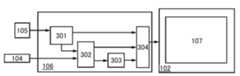
도 1a는 표시 장치의 일 형태를 도시한 블록도이다. 도 1a에 도시된 표시 장치(100)는 화상 데이터 처리부(101) 및 표시부(102)를 갖는다. 화상 데이터 처리부(101)는 제 1 기억 장치(103), 제 2 기억 장치(104), 비교 회로(105), 및 기록 제어 회로(106)를 갖는다. 표시부(102)는 화소부(107)를 갖는다.1A is a block diagram illustrating one embodiment of a display device. The
화상 데이터 처리부(101)는 외부로부터 입력되는 화상 데이터 Data를 유지하고 이 화상 데이터 Data를 표시부(102)에 출력하는 화상 데이터 Data_V로 변환하는 처리를 수행한다. 또한, 화상 데이터 Data 및 화상 데이터 Data_V는 디지털 신호인 것이 바람직하다.The image
표시부(102)에는 화상 데이터 Data_V가 입력되고, 화상 데이터 Data_V에 기초한 비디오 전압이 각 화소의 표시 소자에 기록된다.The image data Data_V is input to the
제 1 기억 장치(103)는 1프레임분의 화상 데이터를 기억한다. 예를 들어, 제 1 기억 장치(103)는 n째 프레임(n은 자연수)의 화상 데이터를 기억할 수 있다. 제 1 기억 장치(103)는 FIFO(first in first out) 메모리의 구조를 갖는 것이 바람직하다. 또한, 제 1 기억 장치(103)로서는 프레임 메모리를 사용할 수 있다. 또한, 제 1 기억 장치(103)에 기억된 n째 프레임의 화상 데이터는 행마다 (n+1)째 프레임의 화상 데이터로 재기록된다. 또한, 제 1 기억 장치(103)에 기억된 n째 프레임의 화상 데이터는 비교 회로(105)에 1행분씩 순차적으로 출력된다. 또한, 제 1 기억 장치(103)는 복수의 프레임 기간의 화상 데이터를 기억할 수 있도록 복수로 제공되어도 좋다.The
제 2 기억 장치(104)는 화소부(107)의 게이트선 1행분에 대응하는 화상 데이터를 기억한다. 예를 들어, 제 2 기억 장치(104)는 (n+1)째 프레임 m째 행(m은 자연수)의 화상 데이터를 기억할 수 있다. 제 2 기억 장치(104)로서는 라인 메모리를 사용할 수 있다. 또한, 제 2 기억 장치(104)에 기억된 (n+1)째 프레임 m째 행의 화상 데이터는 비교 회로(105) 및 제 1 기억 장치(103)에 1행분씩 순차적으로 출력된다. 제 1 기억 장치(103)에서는 n째 프레임 m째 행의 화상 데이터가 제 2 기억 장치(104)에 기억된 (n+1)째 프레임 m째 행의 화상 데이터로 재기록된다.The
비교 회로(105)는 같은 행의 화상 데이터에 상당하는, 제 1 기억 장치(103)에 기억된 화상 데이터와 제 2 기억 장치(104)에 기억된 화상 데이터를 비교하여 일치 또는 불일치를 판정한 판정 데이터를 출력한다. 예를 들어, 비교 회로(105)는 (n+1)째 프레임 m째 행의 화상 데이터와 n째 프레임 m째 행의 화상 데이터를 비교하여 일치 또는 불일치를 판정한 판정 데이터를 기록 제어 회로(106)에 출력한다.The
또한, 화상 데이터간의 일치 또는 불일치 판정은 두 개의 화상 데이터에서의 각 비트의 화상 신호의 배타적 논리합(EX-OR)을 연산하여 판정된다. 그리고, 화소마다 각 비트에서의 일치 또는 불일치를 판정하여 각 화소의 판정 결과의 부정 논리합(NOR)을 연산함으로써 판정 데이터를 얻을 수 있다.Further, the determination of the coincidence or inconsistency between the image data is determined by calculating the exclusive logical sum (EX-OR) of the image signals of each bit in the two image data. Then, the determination data can be obtained by determining the coincidence or inconsistency in each bit for each pixel and calculating a negative logical sum (NOR) of the determination result of each pixel.
기록 제어 회로(106)는 비교 회로(105)로부터 출력된 일치 또는 불일치 판정 데이터에 따라 화상 데이터 Data_V를 표시부(102)에 출력한다. 예를 들어, 기록 제어 회로(106)는 비교 회로(105)의 판정 데이터가 '일치'인 경우 m째 행의 화상 데이터 Data_V를 출력하지 않는다. 또한, 기록 제어 회로(106)는 비교 회로(105)의 판정 데이터가 '불일치'인 경우 표시부(102)의 (n+1)째 프레임 m째 행의 화상 데이터를 화상 데이터 Data_V로서 출력한다. 또한, 기록 제어 회로(106)는 비교 회로(105)의 판정 데이터가 '불일치'이기 때문에 화상 데이터 Data_V가 2프레임 기간 이상 연속하여 출력되는 경우에는, 상기 화상 데이터를 극성이 같은 비디오 전압들로 변환되는 화상 데이터 Data_V로서 출력한다.The
비디오 전압은 데이터선을 통하여 각 화소에 기록하기 위한 화상 데이터에 기초한 전압으로, 액정 소자 등 표시 소자의 한쪽 전극에 인가되는 전압이다. 비디오 전압과 코먼 전위의 차이의 절대값이 같으면 표시 장치에 입력되는 화상 데이터도 같은 값이 된다. 또한, 코먼 전위와의 대소 관계에 따라 표시 소자에 인가되는 비디오 전압의 극성이 전환된다. 예를 들어, 비디오 전압이 코먼 전위보다 큰 경우 표시 소자에 양의 극성의 전압이 인가되고, 비디오 전압이 코먼 전위보다 작은 경우 표시 소자에 음의 극성의 전압이 인가된다.The video voltage is a voltage based on image data for writing to each pixel via a data line and is a voltage applied to one electrode of a display element such as a liquid crystal element. If the absolute value of the difference between the video voltage and the common potential is the same, the image data input to the display device also has the same value. In addition, the polarity of the video voltage applied to the display element is switched in accordance with the magnitude relationship with the common potential. For example, when the video voltage is greater than the common potential, a positive polarity voltage is applied to the display element, and when the video voltage is less than the common potential, a negative polarity voltage is applied to the display element.
화소부(107)에는 m행 k열(k는 자연수)의 화소가 매트릭스 형태로 제공된다. 각 화소는 게이트선 및 데이터선에 접속된 스위칭 소자로서 기능하는 트랜지스터, 및 이 트랜지스터에 접속된 표시 소자를 갖는다.The
도 1b 및 도 1c를 사용하여 화상 데이터 처리부(101)에서의 동작의 일례를 설명한다.An example of the operation in the image
도 1b 및 도 1c의 도면에서 가로 축이 시간을, 세로 축이 화소의 표시 소자에 인가되는 비디오 전압의 크기를 나타내고 있다. 또한, 도 1b 및 도 1c의 도면에서는 가로 축에 n째 프레임 내지 (n+4)째 프레임에서의 m째 행의 같은 열의 화소에 기록되는 비디오 전압의 크기를 차례로 배치하여 나타내었다. 또한, 도 1b 및 도 1c의 도면에서는 m째 행에 화소를 1열만 갖는 구성인 것으로 설명한다. 즉, 도 1b 및 도 1c를 사용하여 설명하는 비디오 전압의 크기가 인접하는 프레임 기간들간에서 같은 경우, 비교 회로(105)에서 비교되는 (n+1)째 프레임 m째 행의 화상 데이터와 n째 프레임 m째 행의 화상 데이터는 일치된다. 또한, 도 1b 및 도 1c를 사용하여 설명하는 비디오 전압의 크기가 인접하는 프레임 기간들간에서 다른 경우, 비교 회로(105)에서 비교되는 (n+1)째 프레임 m째 행의 화상 데이터와 n째 프레임 m째 행의 화상 데이터는 일치되지 않는다.1B and 1C, the horizontal axis represents time and the vertical axis represents the magnitude of the video voltage applied to the display element of the pixel. In addition, in the drawings of FIGS. 1B and 1C, the magnitudes of video voltages recorded in pixels in the same column of the m-th row in the n-th frame to the (n + 4) th frame are shown in order on the horizontal axis. In addition, in the drawings of FIGS. 1B and 1C, the configuration has only one column of pixels in the m-th row. That is, when the magnitude of the video voltage described with reference to FIGS. 1B and 1C is the same between adjacent frame periods, the image data of the (n + 1) th frame m-th row compared to the n-th frame by the
또한, 도 1b에서는 n째 프레임의 비디오 전압의 크기가 |V1|인 것으로 하여 설명한다. 또한, (n+1)째 프레임의 비디오 전압의 크기가 |V1|인 것으로 하여 설명한다. 또한, (n+2)째 프레임의 비디오 전압의 크기가 |V1|인 것으로 하여 설명한다. 또한, (n+3)째 프레임의 비디오 전압의 크기가 |V2|인 것으로 하여 설명한다. 또한, (n+4)째 프레임의 비디오 전압의 크기가 |V2|인 것으로 하여 설명한다. 또한, Vcom은 코먼 전위이다.In addition, in FIG. 1B, it is assumed that the magnitude of the video voltage of the n-th frame is | V1 |. In addition, it is assumed that the magnitude of the video voltage of the (n + 1) th frame is | V1 |. In addition, it is assumed that the magnitude of the video voltage of the (n + 2) th frame is | V1 |. In addition, it is assumed that the magnitude of the video voltage of the (n + 3) th frame is | V2 |. In addition, it is assumed that the magnitude of the video voltage of the (n + 4) th frame is | V2 |. In addition, Vcom is a common potential.
도 1b에 도시된 바와 같이 양의 극성의 비디오 전압 V1이 n째 프레임 내지 (n+2)째 프레임의 비디오 전압으로서 계속하여 공급된다. 또한, 도 1b에 도시된 바와 같이 양의 극성의 비디오 전압 V2가 (n+3)째 프레임 내지 (n+4)째 프레임의 비디오 전압으로서 계속하여 공급된다. 또한, 도 1b에서는 (n+3)째 프레임 내지 (n+4)째 프레임의 비디오 전압의 극성을 양으로 하였지만 음으로 하여도 좋다.As shown in Fig. 1B, the video voltage V1 of positive polarity is continuously supplied as the video voltage of the nth frame to the (n + 2) th frame. Also, as shown in Fig. 1B, the video voltage V2 of positive polarity is continuously supplied as the video voltage of the (n + 3) th frame to the (n + 4) th frame. In addition, although the polarity of the video voltage of the (n + 3) th frame to the (n + 4) th frame is positive in FIG. 1B, it may be negative.
도 1b의 경우, 비교 회로(105)에 의하여 n째 프레임 내지 (n+2)째 프레임 m째 행의 화상 데이터가 비교되어 '일치'의 판정 데이터가 얻어진다. 이 경우 기록 제어 회로(106)는 표시부(102)의 (n+1)째 프레임 m째 행의 화상 데이터를 사용한 기록을 하지 않는다. 마찬가지로, 기록 제어 회로(106)는 표시부(102)의 (n+2)째 프레임 m째 행의 화상 데이터를 사용한 기록을 하지 않는다. 구체적으로는 (n+1)째 프레임 내지 (n+2)째 프레임의 화상 데이터를 사용한 표시 기간에서 화소부(107)의 m째 행 게이트선을 선택하지 않고 화소가 갖는 표시 소자에 비디오 전압을 기록하지 않는다. 도 1b에 있어서 화살표로 나타낸 기간 Woff1은 화상 데이터가 n째 프레임의 화상 데이터와 동일하고 비디오 전압 V1을 다시 기록하지 않는 기간에 상당한다.In the case of FIG. 1B, the
또한, 도 1b의 경우, 비교 회로(105)에 의하여 (n+3)째 프레임 내지 (n+4)째 프레임 m째 행의 화상 데이터가 비교되어 '일치'의 판정 데이터가 얻어진다. 이 경우 기록 제어 회로(106)는 표시부(102)의 (n+4)째 프레임 m째 행의 화상 데이터를 사용한 기록을 하지 않는다. 구체적으로는 (n+4)째 프레임의 화상 데이터를 사용한 표시 기간에서 화소부(107)의 m째 행 게이트선을 선택하지 않고 화소가 갖는 표시 소자에 비디오 전압을 기록하지 않는다. 도 1b에 있어서 화살표로 나타낸 기간 Woff2는 화상 데이터가 (n+3)째 프레임의 화상 데이터와 동일하고 비디오 전압 V2를 다시 기록하지 않는 기간에 상당한다.In addition, in the case of FIG. 1B, the
본 발명의 일 형태의 구성에서는 비교 회로(105)에서 화상 데이터간의 일치 또는 불일치를 판정한 판정 데이터에 따라 기간 Woff1 및 기간 Woff2와 같이 기록 제어 회로(106)가 같은 행의 화소에 비디오 전압을 기록하지 않는 기간을 설정할 수 있다. 이에 의하여 저소비 전력화를 도모할 수 있다.In one configuration of the present invention, the
또한, 도 1c는 도 1b와는 다른, 연속되는 프레임 기간에서의 비디오 전압의 변화에 대하여 도시한 모식도를 도시한 것이다.Also, FIG. 1C shows a schematic diagram showing the change of the video voltage in the continuous frame period different from FIG. 1B.
또한, 도 1c에서는 n째 프레임의 비디오 전압의 크기가 |V1|인 것으로 하여 설명한다. 또한, (n+1)째 프레임의 비디오 전압의 크기가 |V2|인 것으로 하여 설명한다. 또한, (n+2)째 프레임의 비디오 전압의 크기가 |V1|인 것으로 하여 설명한다. 또한, (n+3)째 프레임의 비디오 전압의 크기가 0인 것으로 하여 설명한다. 또한, (n+4)째 프레임의 비디오 전압의 크기가 |V1|인 것으로 하여 설명한다.1C, it is assumed that the magnitude of the video voltage of the n-th frame is | V1 |. In addition, it is assumed that the magnitude of the video voltage of the (n + 1) th frame is | V2 |. In addition, it is assumed that the magnitude of the video voltage of the (n + 2) th frame is | V1 |. In addition, it is assumed that the magnitude of the video voltage of the (n + 3) th frame is zero. In addition, it is assumed that the magnitude of the video voltage of the (n + 4) th frame is | V1 |.
도 1c에 도시된 바와 같이 n째 프레임의 비디오 전압으로서 극성이 양인 비디오 전압 V1이 공급된다. 또한, 도 1c에 도시된 바와 같이 (n+1)째 프레임의 비디오 전압으로서 극성이 양인 비디오 전압 V2가 공급된다. 또한, 도 1c에 도시된 바와 같이 (n+2)째 프레임의 비디오 전압으로서 극성이 양인 비디오 전압 V1이 공급된다. 또한, 도 1c에 도시된 바와 같이 (n+3)째 프레임의 비디오 전압으로서 Vcom이 공급된다. 또한, 도 1c에 도시된 바와 같이 (n+4)째 프레임의 비디오 전압으로서 극성이 음인 비디오 전압 ―V1이 공급된다.As shown in Fig. 1C, the video voltage V1 of positive polarity is supplied as the video voltage of the nth frame. Also, as shown in Fig. 1C, the video voltage V2 of positive polarity is supplied as the video voltage of the (n + 1) th frame. Also, as shown in Fig. 1C, as a video voltage of the (n + 2) th frame, a video voltage V1 of positive polarity is supplied. Also, as shown in Fig. 1C, Vcom is supplied as the video voltage of the (n + 3) th frame. Also, as shown in Fig. 1C, as the video voltage of the (n + 4) th frame, a negative polarity video voltage -V1 is supplied.
일반적으로 표시 소자로서 액정 소자가 사용된 표시 장치에서는 게이트 라인 반전 구동, 소스 라인 반전 구동, 프레임 반전 구동, 도트 반전 구동 등, 1프레임 기간마다 표시 소자에 양과 음의 극성을 교대로 부여하는 반전 구동을 한다. 그러나, 표시 소자에 인가되는 비디오 전압이 큰 경우에 반전 구동을 하면 표시 소자에 인가되는 비디오 전압의 크기가 변화되지 않더라도 비디오 전압의 변화량이 크게 되어 소비 전력이 커진다. 소비 전력의 증대는 구동 주파수가 큰 구동의 경우에 특히 현저하다.In general, in a display device in which a liquid crystal element is used as a display element, an inversion drive that alternately imparts positive and negative polarities to the display element every frame period, such as gate line inversion driving, source line inversion driving, frame inversion driving, and dot inversion driving. Do it. However, if the inversion driving is performed when the video voltage applied to the display element is large, the amount of change in the video voltage becomes large and power consumption increases even if the magnitude of the video voltage applied to the display element does not change. The increase in power consumption is particularly remarkable in the case of driving with a large driving frequency.
상술한 반전 구동에 기인하는 소비 전력의 증대에 대하여 도 1c에 도시된 예를 사용하여 설명한다. 도 1c에 도시된 연속되는 프레임 기간에서의 비디오 전압의 변화에 대한 모식도에 있어서, 프레임 기간마다 반전 구동을 하는 구성으로 한 경우 도 1c에서는 (n+1)째 프레임의 비디오 전압을 음의 극성(굵은 점선으로 나타낸 비디오 전압 ―V2)으로 한다. 이 경우, 같은 화상 데이터라도 극성이 양인 비디오 전압을 인가하는 경우에 비하여 극성이 음인 비디오 전압을 인가하는 경우에는 전후의 프레임 기간과의 사이에서 비디오 전압의 변동이 커진다.The increase in power consumption resulting from the above-mentioned inversion drive is demonstrated using the example shown in FIG. 1C. In the schematic diagram of the change of the video voltage in successive frame periods shown in FIG. 1C, when the inversion driving is performed for each frame period, in FIG. The video voltage represented by the thick dotted line-V2 ). In this case, the variation of the video voltage increases between the frame periods before and after the same image data when the video voltage with the negative polarity is applied as compared with the case where the video voltage with the positive polarity is applied.
한편, 도 1c에 도시된 구동 방법에서는 연속되는 n째 프레임 내지 (n+2)째 프레임에서 표시 소자에 극성이 양인 비디오 전압을 인가하는 구성이다. 본 실시형태에서의 표시 장치의 구동 방법은 비디오 전압을 각 화소에 기록할 때 반전 구동을 하는 빈도를 저감시키는 구성으로 할 수 있다. 즉, 1프레임 기간마다 반전 구동을 하는 것이 아니라 도 1c에 도시된 바와 같이 2프레임 기간 이상 연속하여 극성이 같은 비디오 전압들을 인가하여 기록이 수행된다. 이로써 표시 소자에 인가되는 비디오 전압의 크기가 거의 변화되지 않더라도 1프레임 기간마다 반전 구동을 하는 것으로 인하여 비디오 전압의 변화량이 크게 되는 문제를 저감시킬 수 있어 저소비 전력화를 도모할 수 있다. 또한, 표시 장치에 사용하는 표시 소자에 따라서는 반전 구동을 하지 않고도 동작할 수도 있어 소비 전력을 더 낮게 하는 것도 가능하다.On the other hand, in the driving method shown in Fig. 1C, the video voltage having a positive polarity is applied to the display element in the nth frame to the (n + 2) th frame in succession. The driving method of the display device according to the present embodiment can be configured to reduce the frequency of inversion driving when writing a video voltage to each pixel. That is, instead of performing inversion driving every one frame period, recording is performed by applying video voltages having the same polarity consecutively for two or more frame periods as shown in FIG. 1C. As a result, even if the magnitude of the video voltage applied to the display element is hardly changed, the inversion driving is performed every one frame period, thereby reducing the problem of a large amount of change in the video voltage, thereby achieving low power consumption. In addition, depending on the display elements used in the display device, the display device may operate without inversion driving, and thus the power consumption may be lowered.
다음에, 화상 데이터가 입력되는 제 1 기억 장치(103) 및 제 2 기억 장치(104)의 구성에 대하여 구체적인 예를 들어 설명한다.Next, the structure of the 1st memory |
우선, 도 2a는 제 1 기억 장치(103) 및 제 2 기억 장치(104)에 입력되는 화상 데이터를 구체적으로 설명하기 위하여 3행 4열의 화소를 갖는 화소부에 입력되는 화상 데이터를 도시한 모식도이다. 도 2a는 n째 프레임 및 (n+1)째 프레임의 화상 데이터에 기초한 비디오 전압의 분포에 대하여 도시한 것이다.First, FIG. 2A is a schematic diagram showing image data input to a pixel portion having three rows and four columns of pixels in order to specifically describe image data input to the
도 2a는 n째 프레임의 화상 데이터에 기초한 비디오 전압 V1을 3행 4열의 화소에 입력하는 예를 도시한 것이다. 또한, 도 2a는 (n+1)째 프레임의 화상 데이터에 기초한 비디오 전압 V1 또는 비디오 전압 V2를 3행 4열의 화소에 입력하는 예를 도시한 것이다.FIG. 2A shows an example of inputting a video voltage V1 based on image data of an nth frame to pixels of three rows and four columns. 2A shows an example of inputting the video voltage V1 or the video voltage V2 based on the image data of the (n + 1) th frame to the pixels in three rows and four columns.
도 2b는 도 2a에 도시된 n째 프레임 및 (n+1)째 프레임의 화상 데이터가 제 1 기억 장치(103) 및 제 2 기억 장치(104)에 기억되는 모양을 도시한 모식도이다. 도 2b에 도시된 바와 같이 제 1 기억 장치(103)에서는 n째 프레임의 화상 데이터가 1프레임분의 화상 데이터로서 기억된다. 또한, 제 2 기억 장치(104)에서는 (n+1)째 프레임 1째 행의 화상 데이터가 1행분의 화상 데이터로서 기억된다.FIG. 2B is a schematic diagram showing how image data of the nth frame and the (n + 1) th frame shown in FIG. 2A are stored in the
또한, 도 2b에 도시된 비교 회로(105)는 배타적 논리합 회로(211), 부정 논리합 회로(212)를 갖는다. 배타적 논리합 회로(211)는 제 2 기억 장치(104)에 기억된 화상 데이터 및 제 1 기억 장치(103)에 기억된 1째 행의 화상 데이터를 판독하여 배타적 논리합을 연산한다.In addition, the
예를 들어, n째 프레임 1째 행의 화상 데이터(도 2b에서 점선(201)으로 둘러싸인 화상 데이터)와 (n+1)째 프레임 1째 행의 화상 데이터(도 2b에서 점선(202)으로 둘러싸인 화상 데이터)를 비교한 경우 모두 같은 화상 데이터이며 어느 열의 화상 데이터와도 일치된다. 이 경우, 배타적 논리합 회로(211)는 'LLLL'의 신호를 출력한다. 그리고, 배타적 논리합 회로(211)의 출력이 입력되는 부정 논리합 회로(212)는 'H'를 출력한다. 이 부정 논리합 회로(212)로부터 기록 제어 회로(106)에 출력되는 신호가 판정 데이터이며 이 경우, 이 신호는 화상 데이터가 일치되는 경우의 신호이다.For example, the image data of the first row of the nth frame (the image data surrounded by the dotted
또한, 제 1 기억 장치(103) 및 제 2 기억 장치(104)에 기억되는 화상 데이터가 멀티 비트의 데이터인 경우, 각 비트에서 비교 동작을 하여 논리합을 연산함으로써 화상 데이터의 일치 또는 불일치를 검출하는 구성으로 하면 좋다.In addition, when the image data stored in the
도 2b에 도시된 바와 같이 비교 회로(105)에서 사용된 제 2 기억 장치(104)의 (n+1)째 프레임 m째 행의 화상 데이터는 제 1 기억 장치(103)의 n째 프레임 m째 행의 화상 데이터가 기억된 영역에 덮어 쓰여 기억된다(도 2c에서 점선(203)으로 둘러싸인 화상 데이터). 그리고, 제 2 기억 장치(104)에는 (n+1)째 프레임 2째 행의 화상 데이터가 입력된다. 또한, 본 실시형태의 구성에서는 제 1 기억 장치(103)에 1행분의 화상 데이터를 연속적으로 덮어 써 기억시키는 구성에 대하여 설명하지만 다른 구성으로 하여도 좋다. 예를 들어, 제 1 기억 장치(103)를 홀수 프레임용 기억 장치로서 사용하고 별도로 제공한 기억 장치를 짝수 프레임용 기억 장치로서 사용하는 구성으로 하여도 좋다.As shown in FIG. 2B, the image data of the (n + 1) th mth row of the
또한, n째 프레임 2째 행의 화상 데이터(도 2c에서 점선(204)으로 둘러싸인 화상 데이터)와, (n+1)째 프레임 2째 행의 화상 데이터(도 2c에서 점선(205)으로 둘러싸인 화상 데이터)를 비교한 경우 1째 열과 3째 열의 화상 데이터는 일치되고, 2째 열과 4째 열의 화상 데이터는 일치되지 않는다. 이 경우, 배타적 논리합 회로(211)는 'LHLH'의 신호를 출력한다. 그리고, 배타적 논리합 회로(211)의 출력이 입력되는 부정 논리합 회로(212)는 'L'을 출력한다. 이 부정 논리합 회로(212)로부터 기록 제어 회로(106)에 출력되는 신호가 판정 데이터이며 이 경우, 이 신호는 화상 데이터가 '불일치'인 경우의 신호이다.Further, the image data of the second row of the nth frame (image data surrounded by the dotted
본 실시형태의 구성에서는 행 단위, 즉 게이트선 단위로 앞의 프레임 기간과의 화상 데이터의 변화를 비교하여 기록을 할지 여부의 판정을 하는 구성으로 할 수 있다. 그러므로, 다른 프레임 기간의 화상 데이터를 유지하는 기억 장치를 프레임 메모리와 라인 메모리의 조합으로 할 수 있어, 복수의 프레임 메모리를 사용하여 프레임 기간들을 비교하는 구성에 비하여 제 2 기억 장치(104)의 구성을 간략화할 수 있다.In the structure of this embodiment, it can be set as the structure which judges whether recording is made by comparing the change of image data with a previous frame period in a row unit, ie, a gate line unit. Therefore, the storage device for holding image data of different frame periods can be a combination of the frame memory and the line memory, so that the structure of the
다음에 비교 회로(105)로부터 판정 데이터가 입력되는 기록 제어 회로(106)의 구성에 대하여 구체적인 예를 들어 설명한다.Next, the structure of the
도 3에 도시된 기록 제어 회로(106)는 재기록 판정 회로(301), 전압 변화 판정 회로(302), 반전 신호 생성 회로(303), 및 표시 제어 회로(304)를 갖는다.The
재기록 판정 회로(301)는 비교 회로(105)로부터 입력되는 판정 데이터에 따라 판정한 행의 화상 데이터를 출력할지 여부를 판정하는 회로이다. 화상 데이터를 출력하는 경우, 재기록 판정 회로(301)는 출력하는 화상 데이터가 제 2 기억 장치(104)로부터 전압 변화 판정 회로(302)를 통하여 표시 제어 회로(304)에 출력되게 한다. 화상 데이터를 출력하지 않는 경우, 재기록 판정 회로(301)는 상기 행의 화상 데이터를 표시 제어 회로(304)에 출력하지 않고 상기 행의 게이트선을 선택하지 않도록 제어한다.The
전압 변화 판정 회로(302)는 화상 데이터에 기초한 비디오 전압의 극성을 모니터링하는 회로이다. 구체적으로는 비디오 전압의 극성을 모니터링하여 2프레임 기간 연속하여 극성이 양이 되도록 제어하는 회로이다. 또는, 전압 변화 판정 회로(302)는 화상 데이터에 기초한 비디오 전압의 변화를 모니터링하여, 극성이 양인 상태가 2프레임 기간 이상 계속되는 경우에 비디오 전압의 변화가 크면 비디오 전압의 극성을 음으로 전환시키도록 제어하고, 비디오 전압의 변화가 작으면 비디오 전압의 극성을 양으로 유지하도록 제어한다. 이 구성으로 함으로써 반전 구동을 하는 것으로 인하여 비디오 전압이 크게 변화되는 일을 억제할 수 있어 저소비 전력화를 도모할 수 있다. 또한, 비디오 전압 변화의 대소에 관해서는 예를 들어, 비디오 전압의 최대값의 절반을 기준으로 하여 대소 관계를 산출하는 구성으로 하면 좋다.The voltage
반전 신호 생성 회로(303)는 전압 변화 판정 회로(302)에 의한 제어에 따라 화상 데이터에 기초한 비디오 전압의 극성을 양 또는 음으로 하는 회로이다.The inverted
표시 제어 회로(304)는 각 행의 판정 데이터에 기초하여 처리된 화상 데이터 data_V, 및 표시부(102)에서 표시를 수행하기 위한 제어 신호를 출력하는 회로이다.The
다음에, 상술한 본 실시형태의 구성에 의하여 동작하는 표시 장치의 구동 방법의 일례를 나타낸 타이밍 차트를 사용하여 설명한다.Next, the timing chart which shows an example of the drive method of the display apparatus which operates by the structure of this embodiment mentioned above is demonstrated.
도 4a는 도 2a와 마찬가지로 3행 4열의 화소를 갖는 화소부에 입력되는 화상 데이터를 도시한 모식도이다. 또한, 도 4a는 n째 프레임, (n+1)째 프레임, 및 (n+2)째 프레임의 화상 데이터의 분포에 대하여 도시한 것이다. 또한, 도 4a에서는 화소부의 게이트선에 입력되는 주사 신호를 1째 행부터 각각 Gout1, Gout2, Gout3이라고 불러 설명한다. 또한, 화소부의 데이터선 측에는 각 데이터선에 접속되는 스위치를 제공하고 스위치의 선택 신호를 1째 열부터 각각 Sout1, Sout2, Sout3, 및 Sout4라고 불러 설명한다. 상술한 스위치가 온 상태가 됨으로써 화상 데이터 data_V에 기초하여 생성된 비디오 전압 Video_V가 각 데이터선에 입력된다.FIG. 4A is a schematic diagram showing image data input to a pixel portion having pixels of three rows and four columns as in FIG. 2A. 4A illustrates the distribution of image data of the nth frame, the (n + 1) th frame, and the (n + 2) th frame. In FIG. 4A, the scanning signals inputted to the gate lines of the pixel portion are referred to as Gout1, Gout2, and Gout3 from the first row, respectively. In addition, a switch connected to each data line is provided on the data line side of the pixel portion, and the selection signals of the switches are referred to as Sout1, Sout2, Sout3, and Sout4 from the first column, respectively. When the above switch is turned on, the video voltage Video_V generated based on the image data data_V is input to each data line.
다음에, 도 4b는 n째 프레임, (n+1)째 프레임, 및 (n+2)째 프레임 주사 신호 Gout1, Gout2, Gout3, 선택 신호 Sout1, Sout2, Sout3, 및 Sout4, 및 비디오 전압 Video_V에 대한 타이밍 차트이다.4B shows the nth frame, the (n + 1) th frame, and the (n + 2) th frame scan signals Gout1, Gout2, Gout3, the selection signals Sout1, Sout2, Sout3, and Sout4, and the video voltage Video_V. This is a timing chart.
도 4b에 도시된 타이밍 차트에서는 n째 프레임 이전에 각 화소에 화상 데이터가 기록되지 않은 것으로 설명한다. 그러므로, n째 프레임에서는 화상 데이터 처리부(101)가 n째 프레임의 화상 데이터 data_V를 그대로 출력하고 각 화소에 비디오 전압 Video_V인 V1이 기록되도록 주사 신호 및 선택 신호를 제어하는 것으로 설명한다.In the timing chart shown in FIG. 4B, it is described that image data is not recorded in each pixel before the nth frame. Therefore, in the nth frame, it is explained that the image
다음에, 도 4b에 도시된 타이밍 차트에서는 (n+1)째 프레임에 기록하는 비디오 전압 Video_V를 입력한다. 상술한 바와 같이 본 실시형태의 구성의 표시 장치에서는 판정 데이터가 '일치'인 경우 표시부의 m째 행 화소에 화상 데이터에 기초한 비디오 전압을 기록하지 않고, 판정 데이터가 '불일치'인 경우 표시부의 m째 행 화소에 화상 데이터에 기초한 비디오 전압을 기록한다. 또한, 본 실시형태의 구성의 표시 장치에서 화상 데이터는 2프레임 기간 이상 연속하여 기록되는 경우에는 극성이 같은 비디오 전압들을 인가하여 기록된다. 이 제어에 따라 화상 데이터 처리부(101)는 판정 데이터가 '일치'인 1째 행 비디오 전압 Video_V를 기록하지 않도록 제어하고, 또 판정 데이터가 '불일치'인 2째 행 및 3째 행의 화상 데이터 data_V에 기초한 비디오 전압 Video_V를 양의 극성으로 출력하도록 제어한다.Next, in the timing chart shown in Fig. 4B, the video voltage Video_V recorded in the (n + 1) th frame is input. As described above, in the display device having the configuration of the present embodiment, when the determination data is 'matched', the video voltage based on the image data is not recorded in the m-th pixel of the display portion, and when the determination data is 'unmatched', the display portion m The video voltage based on the image data is recorded in the second row pixel. In addition, in the display device of the configuration of the present embodiment, when image data is continuously recorded for two or more frame periods, image data is recorded by applying video voltages having the same polarity. According to this control, the image
다음에, 도 4b에 도시된 타이밍 차트에서는 (n+2)째 프레임에 기록하는 비디오 전압 Video_V를 입력한다. 상술한 본 실시형태의 구성의 표시 장치의 제어에 따라 화상 데이터 처리부(101)는 판정 데이터가 '일치'인 1째 행의 화상 데이터를 출력하지 않도록 제어하고, 또 판정 데이터가 '불일치'인 2째 행 및 3째 행의 화상 데이터 data_V에 기초한 비디오 전압 Video_V의 극성을 양으로부터 음으로 하는 반전 구동을 하도록 제어한다.Next, in the timing chart shown in Fig. 4B, the video voltage Video_V recorded in the (n + 2) th frame is input. Under the control of the display device of the above-described configuration of the present embodiment, the image
이어서, 도 5a 내지 도 6을 사용하여 표시부(102)의 구성 및 화소부(107)의 구성에 대하여 설명한다.Next, the structure of the
도 5a에 도시된 표시부(102)는 화소부(107), 게이트선 구동 회로(411), 및 데이터선 구동 회로(412)를 갖는다. 화소부(107)는 복수의 화소(400), 복수의 게이트선(401), 및 복수의 데이터선(402)을 갖는다. 또한, 도 5a에서 게이트선 구동 회로(411)는 디코더 회로에 의하여 게이트선(401)을 1행씩 선택하여 비디오 전압의 기록을 제어할 수 있다.The
도 5b는 도 5a에 도시된 화소(400)의 회로의 일례를 도시한 것이다. 도 5b에 도시된 화소(400)는, 게이트가 게이트선(401)에 접속되고 소스 및 드레인 중 한쪽이 데이터선(402)에 접속된 트랜지스터(421)를 갖는다. 또한, 화소(400)는 한쪽 전극이 트랜지스터(421)의 소스 및 드레인 중 다른 쪽에 접속되고 다른 쪽 전극이 유지 용량선에 접속된 용량 소자(422)를 갖는다. 또한, 화소(400)는, 한쪽 전극(화소 전극이라고도 함)이 트랜지스터(421)의 소스 및 드레인 중 다른 쪽, 및 용량 소자(422)의 한쪽 전극에 접속되고 다른 쪽 전극(대향 전극이라고도 함)이 코먼 전위(Vcom)를 공급하는 배선에 접속된 액정 소자(423)를 갖는다. 또한, 트랜지스터(421)는 n채널형 트랜지스터이다.FIG. 5B illustrates an example of a circuit of the
도 6은 디코더 회로의 예를 도시한 것이다. 디코더 회로(500)는 어드레스선 C1, C1b, C2, C2b, C3, C3b, C4, C4b를 통하여 어드레스 신호를 부정 논리곱 회로(501A), 부정 논리곱 회로(501B)에 입력하고 그 출력을 부정 논리합 회로(502)를 통하여 주사 신호 Gout1로서 출력한다. 도 6에 도시된 구성으로 하여 어드레스선의 전위를 제어함으로써 주사 신호 Gout1로 각 행의 화소를 선택적으로 제어할 수 있다.6 shows an example of a decoder circuit. The
상술한 본 실시형태의 구성에 의하여 같은 행의 화소에 비디오 전압을 기록하지 않는 구성으로 할 수 있다. 이에 의하여 저소비 전력화를 도모할 수 있다.According to the above-described configuration of the present embodiment, it is possible to have a configuration in which no video voltage is written to the pixels in the same row. As a result, power consumption can be reduced.
또한, 본 실시형태의 구성에서는 행 단위, 즉 게이트선 단위로 앞의 프레임 기간과의 화상 데이터의 변화를 비교하여 기록을 할지 여부의 판정을 하는 구성으로 할 수 있다. 그러므로, 다른 프레임 기간의 화상 데이터를 유지하는 기억 장치의 구성을 간략화할 수 있다.In addition, in the structure of this embodiment, it can be set as the structure which judges whether recording is made by comparing the change of image data with the previous frame period in a row unit, ie, a gate line unit. Therefore, the configuration of the storage device for holding image data of another frame period can be simplified.
또한, 본 실시형태의 구성에 의하여 비디오 전압을 각 화소에 기록할 때 반전 구동을 하는 빈도를 저감시키는 구성으로 할 수 있다. 이로써 비디오 전압의 크기가 거의 변화되지 않더라도 반전 구동을 하는 것으로 인하여 비디오 전압의 변화량이 크게 되는 문제를 저감시킬 수 있어 저소비 전력화를 도모할 수 있다.In addition, according to the configuration of the present embodiment, the frequency of inversion driving when the video voltage is recorded in each pixel can be reduced. As a result, even if the magnitude of the video voltage is hardly changed, the problem that the amount of change in the video voltage is large due to inversion driving can be reduced, and the power consumption can be reduced.
(실시형태 2)(Embodiment 2)
본 실시형태에서는 연속되는 프레임 기간에서 화상 데이터가 일치될지 여부의 비교를 화소마다 수행하고 비교 결과에 따라 표시부로의 비디오 전압의 기록을 제어하는 구성에 대하여 설명한다.In the present embodiment, a structure for performing comparison of whether or not image data coincides in successive frame periods for each pixel and controlling the recording of the video voltage to the display unit in accordance with the comparison result will be described.
프레임 기간들의 비교의 구성에 대해서는 상술한 실시형태 1에서 설명한 구성과 대략 마찬가지이다. 본 실시형태의 구성에서는 프레임 기간들의 비교를 화소마다 수행한다. 이 비교에 의하여 얻어진 판정 데이터에 따라 화소에 비디오 전압을 기록할지 여부를 선택하는 구성으로 한다.The configuration of the comparison of the frame periods is substantially the same as the configuration described in
다음에, 도 7a 내지 도 8을 사용하여 비디오 전압의 기록 유무를 화소마다 선택할 수 있는 표시부(102D) 및 화소부(107D)의 구성에 대하여 설명한다.Next, the configurations of the
도 7a에 도시된 표시부(102D)는 화소부(107D), 게이트선 구동 회로(411), 및 데이터선 구동 회로(412D)를 갖는다. 화소부(107D)는 복수의 화소(400D), 복수의 게이트선(401), 복수의 데이터선(402), 및 복수의 선택선(601)을 갖는다. 또한, 도 7a에서 데이터선 구동 회로(412D)는 디코더 회로를 갖는다. 데이터선 구동 회로(412D)가 갖는 디코더 회로가 데이터선(402)을 1열씩 선택함으로써 비디오 전압이 기록될 수 있다. 또한, 데이터선 구동 회로(412D)가 갖는 디코더 회로는 소정의 화소를 선택하여 비디오 전압이 기록되도록 선택선(601)을 제어하는 것이 가능하다.The
도 7b는 도 7a에 도시된 화소(400D)의 회로의 일례를 도시한 것이다. 도 7b에 도시된 화소(400D)는, 게이트가 게이트선(401)에 접속되고 소스 및 드레인 중 한쪽이 데이터선(402)에 접속된 트랜지스터(421)를 갖는다. 또한, 화소(400D)는, 게이트가 선택선(601)에 접속되고 소스 및 드레인 중 한쪽이 트랜지스터(421)의 소스 및 드레인 중 다른 쪽에 접속된 트랜지스터(602)를 갖는다. 또한, 화소(400D)는 한쪽 전극이 트랜지스터(602)의 소스 및 드레인 중 다른 쪽에 접속되고 다른 쪽 전극이 유지 용량선에 접속된 용량 소자(422)를 갖는다. 또한, 화소(400D)는, 한쪽 전극(화소 전극이라고도 함)이 트랜지스터(421)의 소스 및 드레인 중 다른 쪽, 및 용량 소자(422)의 한쪽 전극에 접속되고 다른 쪽 전극(대향 전극이라고도 함)이 코먼 전위(Vcom)를 공급하는 배선에 접속된 액정 소자(423)를 갖는다. 또한, 트랜지스터(421) 및 트랜지스터(602)는 n채널형 트랜지스터이다.FIG. 7B illustrates an example of a circuit of the
도 7b에 도시된 화소(400D)는 스위칭 소자인 트랜지스터(421)를 온 상태로 함으로써 행 방향의 화소를 선택하고 아울러 스위칭 소자인 트랜지스터(602)를 온 상태로 함으로써 열 방향의 화소를 선택할 수 있고 소정의 화소로의 비디오 전압의 기록을 할 수 있다.In the
도 8은 디코더 회로를 갖는 데이터선 구동 회로(412)의 예를 도시한 것이다. 디코더 회로(500)는 어드레스선 C1, C1b, C2, C2b, C3, C3b, C4, C4b를 통하여 어드레스 신호를 부정 논리곱 회로(501A), 부정 논리곱 회로(501B)에 입력하고 그 출력을 부정 논리합 회로(502)를 통하여 스위치(611)의 온 또는 오프의 제어 신호, 및 선택선의 선택 신호 Cout1로서 출력한다. 스위치(611)의 한쪽 단자는 비디오 전압 Video_V가 공급되는 배선에 접속되고, 스위치(611)의 다른 쪽 단자는 데이터 신호 Data1이 공급되는 데이터선에 접속된다. 도 8에 도시된 구성으로 하여 어드레스선의 전위를 제어함으로써 주사 신호 Gout1, 선택 신호 Cout, 및 데이터 신호 Data1로 각행 각열의 화소에 선택적으로 비디오 전압을 기록하도록 제어할 수 있다.8 shows an example of a data
본 실시형태는 다른 실시형태에 기재된 구성과 적절히 조합하여 실시할 수 있다.This embodiment can be implemented in appropriate combination with any of the structures described in the other embodiments.
(실시형태 3)(Embodiment 3)
본 실시형태에서는 표시 장치의 외관 및 단면 등을 도시하여 그 구성에 대하여 설명한다. 본 실시형태에서는 표시 소자로서 액정 소자를 사용한 예를 들어 설명한다.In this embodiment, the appearance, the cross section, and the like of the display device are illustrated and the configuration thereof will be described. In this embodiment, the example which used the liquid crystal element as a display element is demonstrated.
또한, 액정 표시 장치란, 커넥터 예를 들어 FPC(Flexible printed circuit) 또는 TAB(Tape Automated Bonding) 테이프 또는 TCP(Tape Carrier Package)가 부착된 모듈, TAB 테이프나 TCP의 끝에 프린트 배선판이 제공된 모듈, 또는 표시 소자에 COG(Chip On Glass) 방식으로 IC(집적 회로)가 직접 실장된 모듈을 모두 액정 표시 장치의 범주에 포함하는 것으로 한다.In addition, a liquid crystal display device is a connector such as a flexible printed circuit (FPC) or Tape Automated Bonding (TAB) tape or a module with a tape carrier package (TCP), a module provided with a printed wiring board at the end of the TAB tape or TCP, or It is assumed that all modules in which ICs (integrated circuits) are directly mounted in a chip on glass (COG) method are included in a display device.
액정 표시 장치의 외관 및 단면에 대하여 도 9의 (a1), (a2), (b)를 사용하여 설명한다. 도 9의 (a1) 및 (a2)는 트랜지스터(4010, 4011) 및 액정 소자(4013)를 제 1 기판(4001)과 제 2 기판(4006) 사이에 실재(4005)로 밀봉한 패널의 평면도이고, 도 9의 (b)는 도 9의 (a1), (a2)의 M-N에서 절단한 단면도에 상당한다.The external appearance and cross section of a liquid crystal display device are demonstrated using FIG. 9 (a1), (a2), (b). 9A and 9A are plan views of panels in which the
제 1 기판(4001) 위에 제공된 화소부(4002)와, 게이트선 구동 회로(4004)를 둘러싸도록 실재(4005)가 제공되어 있다. 또한, 화소부(4002)와 게이트선 구동 회로(4004) 위에 제 2 기판(4006)이 제공되어 있다. 따라서, 화소부(4002)와 게이트선 구동 회로(4004)는 제 1 기판(4001)과 실재(4005)와 제 2 기판(4006)에 의하여 액정층(4008)과 함께 밀봉되어 있다. 또한, 제 1 기판(4001) 위의 실재(4005)로 둘러싸인 영역과는 다른 영역에 별도로 준비된 기판 위에 단결정 반도체막 또는 다결정 반도체막으로 형성된 데이터선 구동 회로(4003)가 실장되어 있다.A
또한, 별도로 형성한 구동 회로의 접속 방식은 특별히 한정되지 않고 COG 방식, 와이어 본딩 방식, 또는 TAB 방식 등을 사용할 수 있다. 도 9의 (a1)는 COG 방식으로 데이터선 구동 회로(4003)를 실장한 예를 도시한 것이고, 도 9의 (a2)는 TAB 방식으로 데이터선 구동 회로(4003)를 실장한 예를 도시한 것이다.In addition, the connection method of the drive circuit formed separately is not specifically limited, A COG system, a wire bonding system, a TAB system, etc. can be used. FIG. 9A illustrates an example in which the data
또한, 제 1 기판(4001) 위에 제공된 화소부(4002)와 게이트선 구동 회로(4004)는 트랜지스터를 복수로 갖고, 도 9의 (b)에서는, 화소부(4002)에 포함된 트랜지스터(4010)와 게이트선 구동 회로(4004)에 포함된 트랜지스터(4011)를 예로서 도시하고 있다. 트랜지스터(4010, 4011) 위에는 절연층(4020, 4021)이 제공되어 있다.In addition, the
트랜지스터(4010, 4011)의 반도체층에는 비정질, 미결정, 다결정, 또는 단결정인 실리콘 또는 게르마늄 등의 박막 형태의 반도체를 적용할 수 있다. 또는, 트랜지스터(4010, 4011)의 반도체층에는 산화물 반도체를 적용할 수 있다. 본 실시형태에서 트랜지스터(4010, 4011)는 n채널형 트랜지스터이다.As the semiconductor layers of the
트랜지스터(4010, 4011)로서는 비도통 상태에 있어서 소스와 드레인 사이를 흐르는 전류(오프 전류)가 낮은 트랜지스터를 사용하는 것이 특히 바람직하다. 여기서, 오프 전류가 낮다는 것은 실온에서 소스와 드레인 사이의 전압을 10V로 한 경우에 채널 폭 1μm당 규격화된 오프 전류가 10zA 이하인 것을 말한다. 이와 같이 오프 전류가 낮은 트랜지스터로서 반도체층에 산화물 반도체를 갖는 트랜지스터를 들 수 있다.As the
상술한 실시형태에서 설명한 바와 같이 본 실시형태의 표시 장치의 구성에서는 비도통 상태를 유지함으로써 기록한 비디오 전압을 유지한다. 그러므로, 기록한 비디오 전압을 유지하기 위하여 전하의 이동을 수반하는 전위의 변동을 억제하는 트랜지스터로서 오프 전류가 낮은 트랜지스터를 사용하는 것이 바람직하다.As described in the above embodiment, in the configuration of the display device of the present embodiment, the recorded video voltage is maintained by maintaining the non-conducting state. Therefore, in order to maintain the recorded video voltage, it is preferable to use a transistor having a low off current as a transistor for suppressing a change in potential accompanied by charge movement.
또한, 액정 소자(4013)가 갖는 화소 전극층(4030)은 트랜지스터(4010)와 접속되어 있다. 그리고, 액정 소자(4013)의 대향 전극층(4031)은 제 2 기판(4006) 위에 형성되어 있다. 화소 전극층(4030)과 대향 전극층(4031)과 액정층(4008)이 중첩된 부분이 액정 소자(4013)에 상당한다. 또한, 화소 전극층(4030), 대향 전극층(4031)에는 각각 배향막으로서 기능하는 절연층(4032, 4033)이 제공되어 있고, 화소 전극층(4030)과 대향 전극층(4031)은 절연층(4032, 4033)을 사이에 개재(介在)하여 액정층(4008)을 협지(挾持)하고 있다.The pixel electrode layer 4030 included in the
또한, 제 1 기판(4001), 제 2 기판(4006)으로서는 투광성 기판을 사용할 수 있고, 유리, 세라믹스, 플라스틱을 사용할 수 있다. 플라스틱으로서는, FRP(Fiberglass-Reinforced Plastics)판, PVF(폴리비닐플루오라이드) 필름, 폴리에스테르 필름, 또는 아크릴 수지 필름을 사용할 수 있다.As the
또한, 구조체(4035)는 절연막을 선택적으로 에칭하여 얻어지는 기둥 형상 스페이서이며, 화소 전극층(4030)과 대향 전극층(4031) 사이의 거리(셀 갭)를 제어하기 위하여 제공되어 있다. 또한, 구 형상 스페이서를 사용하여도 좋다. 또한, 대향 전극층(4031)은 트랜지스터(4010)와 동일한 기판 위에 제공되는 코먼 전위선과 접속되어 있다. 코먼 콘택트부에 의하여, 한 쌍의 기판 사이에 배치된 도전성 입자를 통해 대향 전극층(4031)과 코먼 전위선을 접속시킬 수 있다. 또한, 도전성 입자는 실재(4005)에 포함시킬 수 있다.The
또한, 액정 소자의 표시 모드로서는 TN(Twisted Nematic) 모드, IPS(In-Plane-Switching) 모드, FFS(Fringe Field Switching) 모드, MVA(Multi-domain Vertical Alignment) 모드, PVA(Patterned Vertical Alignment) 모드, ASM(Axially Symmetric aligned Micro-cell) 모드, OCB(Optically Compensated Birefringence) 모드, FLC(Ferroelectric Liquid Crystal) 모드, AFLC(AntiFerroelectric Liquid Crystal) 모드 등을 사용할 수 있다. 또한, 각 표시 모드에 따라 액정 표시 장치의 전극의 구조 등을 적절히 변경할 수 있다.In addition, as a display mode of the liquid crystal device, TN (Twisted Nematic) mode, IPS (In-Plane-Switching) mode, FFS (Fringe Field Switching) mode, MVA (Multi-domain Vertical Alignment) mode, PVA (Patterned Vertical Alignment) mode An ASM (Axis Symmetric aligned Micro-cell) mode, an Optimal Compensated Birefringence (OCB) mode, a Ferroelectric Liquid Crystal (FLC) mode, and an AntiFerroelectric Liquid Crystal (AFLC) mode may be used. Moreover, the structure etc. of the electrode of a liquid crystal display device can be changed suitably according to each display mode.
또한, 배향막을 필요로 하지 않는 블루상(blue phase)을 나타내는 액정을 사용하여도 좋다. 블루상은 액정상의 하나로, 콜레스테릭(cholesteric) 액정을 계속하여 승온한 경우에 콜레스테릭상으로부터 등방상으로 전이하기 직전에 발현되는 상이다. 블루상은 좁은 온도 범위에서밖에 발현되지 않기 때문에 온도 범위를 개선하기 위하여 5wt% 이상의 키랄제를 혼합시킨 액정 조성물을 사용하여 액정층(4008)에 사용한다. 블루상을 나타내는 액정과 키랄제를 포함한 액정 조성물은 응답 속도가 1msec 이하로 짧고 광학적 등방성을 갖기 때문에 배향 처리가 불필요하며 시야각 의존성이 작다.Moreover, you may use the liquid crystal which shows the blue phase which does not require an alignment film. The blue phase is one of the liquid crystal phases and is a phase which is expressed immediately before transition from the cholesteric phase to the isotropic phase when the cholesteric liquid crystal is continuously heated. Since the blue phase is expressed only in a narrow temperature range, in order to improve the temperature range, the blue phase is used in the
또한, 본 실시형태는 투과형 액정 표시 장치 외에 반투과형 액정 표시 장치에도 적용할 수 있다.In addition to the transmissive liquid crystal display device, the present embodiment can be applied to a transflective liquid crystal display device.
또한, 본 실시형태에서는 기판의 외측(시인하는 측)에 편광판을 제공하고, 내측에 착색층, 표시 소자에 사용하는 전극층을 순차적으로 제공한 액정 표시 장치의 예를 나타내었지만 편광판은 기판 내측에 제공되어도 좋다. 또한, 편광판과 착색층의 적층 구조도 본 실시형태에 나타내는 것에 한정되지 않고, 편광판 및 착색층의 재료나 제조 공정의 조건에 따라 적절히 설정하면 좋다. 또한, 표시부 외의 부분에 블랙 매트릭스로서 기능하는 차광막을 제공하여도 좋다.In addition, in this embodiment, although the polarizing plate was provided in the outer side (viewing side) of the board | substrate, and the example provided the liquid crystal display device which provided the colored layer and the electrode layer used for a display element sequentially inside, the polarizing plate is provided in a board | substrate inside. You may be. In addition, the laminated structure of a polarizing plate and a colored layer is not limited to what is shown in this embodiment, What is necessary is just to set suitably according to the material of a polarizing plate and a colored layer, and the conditions of a manufacturing process. In addition, a light shielding film functioning as a black matrix may be provided in a portion other than the display portion.
트랜지스터(4010) 및 트랜지스터(4011)는 반도체층 외에 게이트 절연층, 게이트 전극층, 및 배선층(소스 배선층이나 용량 배선층 등)으로 구성된다.The
또한, 트랜지스터(4010) 및 트랜지스터(4011) 위에는 절연층(4020)이 형성되어 있다. 절연층(4020)으로서는 예를 들어, RF 스퍼터링법으로 질화 실리콘막을 형성한다.In addition, an insulating layer 4020 is formed over the
또한, 평탄화 절연막으로서 절연층(4021)을 형성한다. 절연층(4021)으로서는 폴리이미드, 아크릴, 벤조사이클로부텐계 수지, 폴리아미드, 에폭시 등 내열성을 갖는 유기 재료를 사용할 수 있다. 또한, 이들 유기 재료 외에 저유전율 재료(low-k 재료), 실록산계 수지, PSG(phosphosilicate glass), BPSG(borophosphosilicate glass) 등을 사용할 수 있다. 또한, 이들 재료로 형성되는 절연막을 복수로 적층시켜 절연층(4021)을 형성하여도 좋다.An insulating
화소 전극층(4030), 대향 전극층(4031)에는 산화 텅스텐을 포함한 인듐 산화물, 산화 텅스텐을 포함한 인듐 아연 산화물, 산화 티타늄을 포함한 인듐 산화물, 산화 티타늄을 포함한 인듐 주석 산화물, 산화 인듐 주석, 인듐 아연 산화물, 산화 실리콘이 첨가된 인듐 주석 산화물 등 투광성을 갖는 도전성 재료를 사용할 수 있다.The pixel electrode layer 4030 and the
화소 전극층(4030), 대향 전극층(4031)으로서 π전자 공액계 도전성 고분자를 사용할 수도 있다. 예를 들어, 폴리아닐린 또는 그 유도체, 폴리피롤 또는 그 유도체, 폴리티오펜 또는 그 유도체, 또는 아닐린, 피롤, 및 티오펜 중 2종류 이상으로 이루어진 공중합체 또는 그 유도체 등을 들 수 있다.(Pi) electron conjugated conductive polymer can also be used as the pixel electrode layer 4030 and the
또한 별도로 형성된 데이터선 구동 회로(4003)와, 게이트선 구동 회로(4004), 또는 화소부(4002)에 공급되는 각종 신호 및 전위는 FPC(4018)로부터 공급된다.In addition, various signals and potentials supplied to the separately formed data
접속 단자 전극(4015)은 액정 소자(4013)가 갖는 화소 전극층(4030)과 동일한 도전막으로 형성되고, 단자 전극(4016)은 트랜지스터(4010, 4011)의 소스 전극층 및 드레인 전극층과 동일한 도전막으로 형성되어 있다.The
접속 단자 전극(4015)은 이방성 도전막(4019)을 통하여 FPC(4018)가 갖는 단자와 전기적으로 접속되어 있다.The
또한, 도 9의 (a1), (a2), 및 (b)는 데이터선 구동 회로(4003)를 별도로 형성하여 제 1 기판(4001)에 실장한 예를 도시한 것이지만 이 구성에 한정되지 않는다. 게이트선 구동 회로를 별도로 형성하여 실장하여도 좋고, 데이터선 구동 회로의 일부 또는 게이트선 구동 회로의 일부만을 별도로 형성하여 실장하여도 좋다.9A, 9A, and 9B show an example in which the data
본 실시형태는 다른 실시형태에 기재된 구성과 적절히 조합하여 실시할 수 있다.This embodiment can be implemented in appropriate combination with any of the structures described in the other embodiments.
(실시형태 4)(Embodiment 4)
본 실시형태에서는 상술한 실시형태에서 설명한 표시 장치가 구비된 전자 기기의 예에 대하여 설명한다.In this embodiment, an example of the electronic device with the display device described in the above-described embodiment will be described.
도 10a에 도시된 휴대형 게임기는 하우징(9630), 표시부(9631), 스피커(9633), 조작 키(9635), 접속 단자(9636), 기록 매체 판독부(9672) 등을 가질 수 있다. 도 10a에 도시된 휴대형 게임기는 기록 매체에 기록된 프로그램 또는 데이터를 판독하여 표시부에 표시하는 기능, 무선 통신에 의하여 다른 휴대형 게임기와 정보를 공유하는 기능 등을 가질 수 있다. 또한, 도 10a에 도시된 휴대형 게임기가 갖는 기능은 이들에 한정되지 않고 다양한 기능을 가질 수 있다.The portable game machine shown in Fig. 10A may have a
도 10b에 도시된 디지털 카메라는 하우징(9630), 표시부(9631), 스피커(9633), 조작 키(9635), 접속 단자(9636), 셔터 버튼(9676), 수상부(9677) 등을 가질 수 있다. 도 10b에 도시된 텔레비전 수상 기능을 갖는 디지털 카메라는 정지 화상을 촬영하는 기능, 동영상을 촬영하는 기능, 촬영한 화상을 자동으로 또는 수동으로 보정하는 기능, 안테나로 다양한 정보를 취득하는 기능, 촬영한 화상 또는 안테나로 취득한 정보를 저장하는 기능, 촬영한 화상 또는 안테나로 취득한 정보를 표시부에 표시하는 기능 등을 가질 수 있다. 또한, 도 10b에 도시된 텔레비전 수상 기능을 갖는 디지털 카메라가 갖는 기능은 이들에 한정되지 않고 다양한 기능을 가질 수 있다.The digital camera shown in FIG. 10B may have a
도 10c에 도시된 텔레비전 수상기는 하우징(9630), 표시부(9631), 스피커(9633), 조작 키(9635), 접속 단자(9636) 등을 가질 수 있다. 도 10c에 도시된 텔레비전 수상기는 텔레비전용 전파를 처리하여 화상 신호로 변환하는 기능, 화상 신호를 처리하여 표시에 적합한 신호로 변환하는 기능, 화상 신호의 프레임 주파수를 변환하는 기능 등을 가질 수 있다. 또한, 도 10c에 도시된 텔레비전 수상기가 갖는 기능은 이들에 한정되지 않고 다양한 기능을 가질 수 있다.The television receiver shown in FIG. 10C may have a
도 11a에 도시된 컴퓨터는 하우징(9630), 표시부(9631), 스피커(9633), 조작 키(9635), 접속 단자(9636), 포인팅 디바이스(9681), 외부 접속 포트(9680) 등을 가질 수 있다. 도 11a에 도시된 컴퓨터는 여러 가지 정보(정지 화상, 동영상, 텍스트 화상 등)를 표시부에 표시하는 기능, 여러 가지 소프트웨어(프로그램)에 의하여 처리를 제어하는 기능, 무선 통신 또는 유선 통신 등 통신 기능, 통신 기능을 이용하여 다양한 컴퓨터 네트워크에 접속하는 기능, 통신 기능을 이용하여 여러 가지 데이터의 송신 또는 수신을 행하는 기능 등을 가질 수 있다. 도 11a에 도시된 컴퓨터가 갖는 기능은 이들에 한정되지 않고 다양한 기능을 가질 수 있다.The computer shown in FIG. 11A may have a
다음에, 도 11b에 도시된 휴대 전화는 하우징(9630), 표시부(9631), 스피커(9633), 조작 키(9635), 마이크로폰(9638), 외부 접속 포트(9680) 등을 가질 수 있다. 도 11b에 도시된 휴대 전화는 여러 가지 정보(정지 화상, 동영상, 텍스트 화상 등)를 표시부에 표시하는 기능, 달력, 날짜, 또는 시각 등을 표시부에 표시하는 기능, 표시부에 표시한 정보를 조작 또는 편집하는 기능, 여러 가지 소프트웨어(프로그램)에 의하여 처리를 제어하는 기능 등을 가질 수 있다. 도 11b에 도시된 휴대 전화가 갖는 기능은 이들에 한정되지 않고 다양한 기능을 가질 수 있다.Next, the mobile telephone shown in FIG. 11B may have a
다음에, 도 11c에 도시된 전자 종이(E-book라고도 함)는 하우징(9630), 표시부(9631), 조작 키(9635) 등을 가질 수 있다. 도 11c에 도시된 전자 종이는 여러 가지 정보(정지 화상, 동영상, 텍스트 화상 등)를 표시부에 표시하는 기능, 달력, 날짜, 또는 시각 등을 표시부에 표시하는 기능, 표시부에 표시한 정보를 조작 또는 편집하는 기능, 여러 가지 소프트웨어(프로그램)에 의하여 처리를 제어하는 기능 등을 가질 수 있다. 도 11c에 도시된 전자 종이가 갖는 기능은 이들에 한정되지 않고 다양한 기능을 가질 수 있다.Next, the electronic paper (also referred to as an E-book) shown in FIG. 11C may have a
본 실시형태에 기재된 전자 기기는 상술한 실시형태에서 설명한 표시 장치를 가짐으로써 저소비 전력화를 실현될 수 있다.The electronic device described in this embodiment can realize low power consumption by having the display device described in the above-described embodiment.
본 실시형태는 다른 실시형태에 기재된 구성과 적절히 조합하여 실시할 수 있다.This embodiment can be implemented in appropriate combination with any of the structures described in the other embodiments.
C1 내지 C4: 어드레스선
Cout1 내지 Cout4: 선택 신호
Data1 내지 Data4: 데이터 신호
Gout1 내지 Gout4: 주사 신호
Sout1 내지 Sout4: 선택 신호
100: 표시 장치
101: 화상 데이터 처리부
102: 표시부
102D: 표시부
103: 기억 장치
104: 기억 장치
105: 비교 회로
106: 제어 회로
107: 화소부
107D: 화소부
201: 점선
202: 점선
203: 점선
204: 점선
205: 점선
211: 배타적 논리합 회로
212: 부정 논리합 회로
301: 판정 회로
302: 전압 변화 판정 회로
303: 반전 신호 생성 회로
304: 표시 제어 회로
400: 화소
400D: 화소
401: 게이트선
402: 데이터선
411: 게이트선 구동 회로
412: 데이터선 구동 회로
412D: 데이터선 구동 회로
421: 트랜지스터
422: 용량 소자
423: 액정 소자
500: 디코더 회로
501A: 부정 논리곱 회로
501B: 부정 논리곱 회로
502: 부정 논리합 회로
601: 선택선
602: 트랜지스터
611: 스위치
4001: 기판
4002: 화소부
4003: 데이터선 구동 회로
4004: 게이트선 구동 회로
4005: 실재
4006: 기판
4008: 액정층
4010: 트랜지스터
4011: 트랜지스터
4013: 액정 소자
4015: 접속 단자 전극
4016: 단자 전극
4018: FPC
4019: 이방성 도전막
4020: 절연층
4021: 절연층
4030: 화소 전극층
4031: 대향 전극층
4032: 절연층
4033: 절연층
4035: 구조체
9630: 하우징
9631: 표시부
9633: 스피커
9635: 조작 키
9636: 접속 단자
9638: 마이크로폰
9672: 기록 매체 판독부
9676: 셔터 버튼
9677: 수상부
9680: 외부 접속 포트
9681: 포인팅 디바이스C1 to C4: address line
Cout1 to Cout4: selection signal
Data1 to Data4: Data Signal
Gout1 to Gout4: scan signal
Sout1 to Sout4: Selection Signal
100: display device
101: image data processing unit
102: display unit
102D: display unit
103: storage device
104: memory device
105: comparison circuit
106: control circuit
107: pixel portion
107D: pixel portion
201: dotted line
202: dotted line
203: dotted line
204: dotted line
205: dotted line
211: exclusive OR circuit
212: Negative Sum Circuit
301: judgment circuit
302: voltage change determination circuit
303: inverted signal generation circuit
304: display control circuit
400 pixels
400D: pixel
401: gate line
402: data line
411: gate line driving circuit
412: data line driving circuit
412D: data line driver circuit
421 transistors
422: capacitive element
423: liquid crystal element
500: decoder circuit
501A: Negative AND Circuit
501B: Negative AND Circuit
502: Negative Sum Circuit
601: selection line
602 transistor
611: switch
4001: substrate
4002: pixel portion
4003: data line driving circuit
4004: gate line driving circuit
4005: Real
4006: substrate
4008: liquid crystal layer
4010: transistor
4011: transistor
4013: liquid crystal element
4015: connecting terminal electrode
4016: terminal electrode
4018: FPC
4019: anisotropic conductive film
4020: insulation layer
4021: insulation layer
4030: pixel electrode layer
4031: counter electrode layer
4032: insulation layer
4033: insulation layer
4035: structure
9630: housing
9631: display unit
9633: speaker
9635: operation keys
9636: connection terminal
9638: microphone
9672: recording medium reading unit
9676: Shutter Button
9677: award
9680: external connection port
9681: pointing device
Claims (10)
Translated fromKoreann째 프레임(n은 자연수)의 화상 데이터를 기억하는 제 1 기억 장치;
(n+1)째 프레임의 화상 데이터의 m째 행(m은 자연수)을 기억하는 제 2 기억 장치;
화소부를 제어하는 기입 제어 회로; 및
제 1 데이터와 제 2 데이터의 일치 또는 불일치를 나타내는 판정 데이터를 생성하는 비교 회로를 포함하고,
상기 제 1 데이터는 상기 제 1 기억 장치 내의 m째 행의 화상 데이터이고,
상기 제 2 데이터는 상기 제 2 기억 장치 내의 m째 행의 화상 데이터이고,
상기 판정 데이터는 상기 기입 제어 회로에 입력되고,
상기 기입 제어 회로는 상기 판정 데이터가 상기 제 1 데이터와 상기 제 2 데이터의 불일치를 나타내는 경우, 상기 화소부의 m째 행의 게이트선을 선택하고,
상기 m째 행의 게이트선이 2 프레임 기간 이상 연속하여 선택되며 화상 데이터에 따른 비디오 전압의 변화가 작은 경우, 극성이 같은 비디오 전압이 상기 화소부에 입력되고,
상기 m째 행의 게이트선이 2 프레임 기간 이상 연속하여 선택되며 비디오 전압의 변화가 큰 경우, 극성이 다른 비디오 전압이 상기 화소부에 입력되는, 반도체 장치.
As a semiconductor device,
a first storage device for storing image data of the nth frame (n is a natural number);
a second memory device for storing the mth row (m is a natural number) of the image data of the (n + 1) th frame;
A write control circuit for controlling the pixel portion; And
A comparison circuit for generating determination data indicating a match or inconsistency of the first data and the second data,
The first data is image data of the m-th row in the first storage device,
The second data is image data of the m-th row in the second storage device,
The determination data is input to the write control circuit,
The write control circuit selects a gate line of an m-th row of the pixel portion when the determination data indicates a mismatch between the first data and the second data,
When the gate line of the m-th row is continuously selected for two or more frame periods and the change of the video voltage according to the image data is small, a video voltage having the same polarity is input to the pixel portion,
And a video voltage having a different polarity is input to the pixel portion when the gate line of the mth row is continuously selected for two or more frame periods and the change in the video voltage is large.
Applications Claiming Priority (2)
| Application Number | Priority Date | Filing Date | Title |
|---|---|---|---|
| JP2012147337 | 2012-06-29 | ||
| JPJP-P-2012-147337 | 2012-06-29 |
Publications (2)
| Publication Number | Publication Date |
|---|---|
| KR20140002497A KR20140002497A (en) | 2014-01-08 |
| KR102082794B1true KR102082794B1 (en) | 2020-02-28 |
Family
ID=49777629
Family Applications (1)
| Application Number | Title | Priority Date | Filing Date |
|---|---|---|---|
| KR1020130069164AExpired - Fee RelatedKR102082794B1 (en) | 2012-06-29 | 2013-06-17 | Method of driving display device, and display device |
Country Status (3)
| Country | Link |
|---|---|
| US (1) | US9508276B2 (en) |
| JP (1) | JP6190180B2 (en) |
| KR (1) | KR102082794B1 (en) |
Families Citing this family (14)
| Publication number | Priority date | Publication date | Assignee | Title |
|---|---|---|---|---|
| JP6807725B2 (en) | 2015-12-22 | 2021-01-06 | 株式会社半導体エネルギー研究所 | Semiconductor devices, display panels, and electronic devices |
| US10490142B2 (en) | 2016-01-29 | 2019-11-26 | Semiconductor Energy Laboratory Co., Ltd. | Semiconductor device, display device, and electronic device |
| JP6906978B2 (en) | 2016-02-25 | 2021-07-21 | 株式会社半導体エネルギー研究所 | Semiconductor devices, semiconductor wafers, and electronics |
| JP2018013765A (en) | 2016-04-28 | 2018-01-25 | 株式会社半導体エネルギー研究所 | Electronic devices |
| TWI743115B (en) | 2016-05-17 | 2021-10-21 | 日商半導體能源硏究所股份有限公司 | Display device and method for operating the same |
| TWI753908B (en) | 2016-05-20 | 2022-02-01 | 日商半導體能源硏究所股份有限公司 | Semiconductor device, display device, and electronic device |
| US10490116B2 (en) | 2016-07-06 | 2019-11-26 | Semiconductor Energy Laboratory Co., Ltd. | Semiconductor device, memory device, and display system |
| JP7044495B2 (en) | 2016-07-27 | 2022-03-30 | 株式会社半導体エネルギー研究所 | Semiconductor device |
| US10755662B2 (en) | 2017-04-28 | 2020-08-25 | Samsung Electronics Co., Ltd. | Display driving circuit and operating method thereof |
| JP7161869B2 (en)* | 2018-06-18 | 2022-10-27 | 株式会社デンソーテン | VIDEO PROCESSING DEVICE AND DISPLAY MODE CHANGE METHOD |
| US20200020271A1 (en)* | 2018-07-13 | 2020-01-16 | Innolux Corporation | Display device |
| KR102617390B1 (en) | 2019-02-15 | 2023-12-27 | 삼성디스플레이 주식회사 | Display device and method for driving the same |
| KR102684198B1 (en)* | 2020-06-25 | 2024-07-11 | 매그나칩믹스드시그널 유한회사 | Panel control circuit and display device including the same |
| CN114822385A (en)* | 2022-05-27 | 2022-07-29 | 中科芯集成电路有限公司 | Write protection circuit of LED display driving chip |
Citations (4)
| Publication number | Priority date | Publication date | Assignee | Title |
|---|---|---|---|---|
| JP2002278523A (en)* | 2001-01-12 | 2002-09-27 | Sharp Corp | Display device driving method and display device |
| JP2005326633A (en) | 2004-05-14 | 2005-11-24 | Nec Electronics Corp | Controller driver and display apparatus |
| JP2008225424A (en) | 2007-03-14 | 2008-09-25 | Samsung Electronics Co Ltd | Liquid crystal display |
| US20110090207A1 (en)* | 2009-10-21 | 2011-04-21 | Semiconductor Energy Laboratory Co., Ltd. | Display device and electronic device including display device |
Family Cites Families (189)
| Publication number | Priority date | Publication date | Assignee | Title |
|---|---|---|---|---|
| US4128901A (en) | 1977-08-17 | 1978-12-05 | Owens-Illinois, Inc. | Ground-reference power supply for gas discharge display/memory panel driving and addressing circuitry |
| JPS60198861A (en) | 1984-03-23 | 1985-10-08 | Fujitsu Ltd | Thin film transistor |
| EP0252646B1 (en) | 1986-07-07 | 1993-09-29 | Semiconductor Energy Laboratory Co., Ltd. | Paperless portable book |
| JPH0244256B2 (en) | 1987-01-28 | 1990-10-03 | Kagaku Gijutsucho Mukizaishitsu Kenkyushocho | INGAZN2O5DESHIMESARERUROTSUHOSHOKEINOSOJOKOZOOJUSURUKAGOBUTSUOYOBISONOSEIZOHO |
| JPH0244260B2 (en) | 1987-02-24 | 1990-10-03 | Kagaku Gijutsucho Mukizaishitsu Kenkyushocho | INGAZN5O8DESHIMESARERUROTSUHOSHOKEINOSOJOKOZOOJUSURUKAGOBUTSUOYOBISONOSEIZOHO |
| JPS63210023A (en) | 1987-02-24 | 1988-08-31 | Natl Inst For Res In Inorg Mater | Compound having a hexagonal layered structure represented by InGaZn↓4O↓7 and its manufacturing method |
| JPH0244258B2 (en) | 1987-02-24 | 1990-10-03 | Kagaku Gijutsucho Mukizaishitsu Kenkyushocho | INGAZN3O6DESHIMESARERUROTSUHOSHOKEINOSOJOKOZOOJUSURUKAGOBUTSUOYOBISONOSEIZOHO |
| JPH0244262B2 (en) | 1987-02-27 | 1990-10-03 | Kagaku Gijutsucho Mukizaishitsu Kenkyushocho | INGAZN6O9DESHIMESARERUROTSUHOSHOKEINOSOJOKOZOOJUSURUKAGOBUTSUOYOBISONOSEIZOHO |
| JPH0244263B2 (en) | 1987-04-22 | 1990-10-03 | Kagaku Gijutsucho Mukizaishitsu Kenkyushocho | INGAZN7O10DESHIMESARERUROTSUHOSHOKEINOSOJOKOZOOJUSURUKAGOBUTSUOYOBISONOSEIZOHO |
| JPH02217893A (en)* | 1989-02-18 | 1990-08-30 | Fujitsu Ltd | Projection type liquid crystal display device |
| JPH0772821B2 (en) | 1990-06-25 | 1995-08-02 | セイコーエプソン株式会社 | Liquid crystal display manufacturing method |
| JPH04255822A (en) | 1991-02-08 | 1992-09-10 | Fujitsu Ltd | liquid crystal display device |
| JPH05251705A (en) | 1992-03-04 | 1993-09-28 | Fuji Xerox Co Ltd | Thin-film transistor |
| JP3118682B2 (en) | 1992-12-25 | 2000-12-18 | キヤノン株式会社 | Liquid crystal display |
| JP3243583B2 (en) | 1992-12-29 | 2002-01-07 | キヤノン株式会社 | Active matrix type liquid crystal display |
| JP3222691B2 (en)* | 1994-07-04 | 2001-10-29 | キヤノン株式会社 | Change line detection apparatus and method |
| JP3479375B2 (en) | 1995-03-27 | 2003-12-15 | 科学技術振興事業団 | Metal oxide semiconductor device in which a pn junction is formed with a thin film transistor made of a metal oxide semiconductor such as cuprous oxide, and methods for manufacturing the same |
| JP3234131B2 (en)* | 1995-06-23 | 2001-12-04 | 株式会社東芝 | Liquid crystal display |
| KR100394896B1 (en) | 1995-08-03 | 2003-11-28 | 코닌클리케 필립스 일렉트로닉스 엔.브이. | A semiconductor device including a transparent switching element |
| KR0155890B1 (en) | 1995-09-28 | 1998-12-15 | 윤종용 | Multi-gradation display driving method of image display device |
| JP3625598B2 (en) | 1995-12-30 | 2005-03-02 | 三星電子株式会社 | Manufacturing method of liquid crystal display device |
| JP3496431B2 (en)* | 1997-02-03 | 2004-02-09 | カシオ計算機株式会社 | Display device and driving method thereof |
| JPH10240191A (en) | 1997-02-24 | 1998-09-11 | Seiko Epson Corp | Information device display device, driving method thereof, and information device |
| JP3883641B2 (en) | 1997-03-27 | 2007-02-21 | 株式会社半導体エネルギー研究所 | Contact structure and active matrix display device |
| KR100266212B1 (en) | 1997-05-17 | 2000-09-15 | 구본준; 론 위라하디락사 | Lcd with the function of removing residual image |
| JP4170454B2 (en) | 1998-07-24 | 2008-10-22 | Hoya株式会社 | Article having transparent conductive oxide thin film and method for producing the same |
| JP2000150861A (en) | 1998-11-16 | 2000-05-30 | Tdk Corp | Oxide thin film |
| JP3276930B2 (en) | 1998-11-17 | 2002-04-22 | 科学技術振興事業団 | Transistor and semiconductor device |
| US6278428B1 (en) | 1999-03-24 | 2001-08-21 | Intel Corporation | Display panel |
| JP3466951B2 (en) | 1999-03-30 | 2003-11-17 | 株式会社東芝 | Liquid crystal display |
| JP3556150B2 (en) | 1999-06-15 | 2004-08-18 | シャープ株式会社 | Liquid crystal display method and liquid crystal display device |
| TW460731B (en) | 1999-09-03 | 2001-10-21 | Ind Tech Res Inst | Electrode structure and production method of wide viewing angle LCD |
| JP4781518B2 (en) | 1999-11-11 | 2011-09-28 | 三星電子株式会社 | Reflective transmission composite thin film transistor liquid crystal display |
| TW494382B (en) | 2000-03-22 | 2002-07-11 | Toshiba Corp | Display apparatus and driving method of display apparatus |
| JP3465886B2 (en) | 2000-03-31 | 2003-11-10 | シャープ株式会社 | Liquid crystal display device and its driving circuit |
| CN1220098C (en) | 2000-04-28 | 2005-09-21 | 夏普株式会社 | Display device, display device driving method, and electronic equipment incorporating display device |
| TW518552B (en) | 2000-08-18 | 2003-01-21 | Semiconductor Energy Lab | Liquid crystal display device, method of driving the same, and method of driving a portable information device having the liquid crystal display device |
| JP2002140052A (en)* | 2000-08-23 | 2002-05-17 | Semiconductor Energy Lab Co Ltd | Portable information device and its driving method |
| JP4089858B2 (en) | 2000-09-01 | 2008-05-28 | 国立大学法人東北大学 | Semiconductor device |
| JP3842030B2 (en) | 2000-10-06 | 2006-11-08 | シャープ株式会社 | Active matrix display device and driving method thereof |
| KR20020038482A (en) | 2000-11-15 | 2002-05-23 | 모리시타 요이찌 | Thin film transistor array, method for producing the same, and display panel using the same |
| JP2002162938A (en) | 2000-11-22 | 2002-06-07 | Toshiba Corp | Liquid crystal display |
| JP2002229532A (en) | 2000-11-30 | 2002-08-16 | Toshiba Corp | Liquid crystal display device and driving method of liquid crystal display device |
| US20030058543A1 (en) | 2001-02-21 | 2003-03-27 | Sheedy James B. | Optically corrective lenses for a head-mounted computer display |
| JP3997731B2 (en) | 2001-03-19 | 2007-10-24 | 富士ゼロックス株式会社 | Method for forming a crystalline semiconductor thin film on a substrate |
| JP2002289859A (en) | 2001-03-23 | 2002-10-04 | Minolta Co Ltd | Thin film transistor |
| JP2002287681A (en) | 2001-03-27 | 2002-10-04 | Mitsubishi Electric Corp | Partial hold type display control device and partial hold type display control method |
| JP3895952B2 (en) | 2001-08-06 | 2007-03-22 | 日本電気株式会社 | Transflective liquid crystal display device and manufacturing method thereof |
| JP3925839B2 (en) | 2001-09-10 | 2007-06-06 | シャープ株式会社 | Semiconductor memory device and test method thereof |
| JP4090716B2 (en) | 2001-09-10 | 2008-05-28 | 雅司 川崎 | Thin film transistor and matrix display device |
| JP4111785B2 (en) | 2001-09-18 | 2008-07-02 | シャープ株式会社 | Liquid crystal display |
| TW574529B (en) | 2001-09-28 | 2004-02-01 | Tokyo Shibaura Electric Co | Organic electro-luminescence display device |
| JP4050119B2 (en) | 2001-10-02 | 2008-02-20 | シャープ株式会社 | Liquid crystal display |
| JP3899886B2 (en) | 2001-10-10 | 2007-03-28 | 株式会社日立製作所 | Image display device |
| JP4164562B2 (en) | 2002-09-11 | 2008-10-15 | 独立行政法人科学技術振興機構 | Transparent thin film field effect transistor using homologous thin film as active layer |
| WO2003040441A1 (en) | 2001-11-05 | 2003-05-15 | Japan Science And Technology Agency | Natural superlattice homologous single crystal thin film, method for preparation thereof, and device using said single crystal thin film |
| KR100940342B1 (en) | 2001-11-13 | 2010-02-04 | 가부시키가이샤 한도오따이 에네루기 켄큐쇼 | Display device and driving method |
| JP4014895B2 (en) | 2001-11-28 | 2007-11-28 | 東芝松下ディスプレイテクノロジー株式会社 | Display device and driving method thereof |
| JP4083486B2 (en) | 2002-02-21 | 2008-04-30 | 独立行政法人科学技術振興機構 | Method for producing LnCuO (S, Se, Te) single crystal thin film |
| CN1445821A (en) | 2002-03-15 | 2003-10-01 | 三洋电机株式会社 | Forming method of ZnO film and ZnO semiconductor layer, semiconductor element and manufacturing method thereof |
| JP3933591B2 (en) | 2002-03-26 | 2007-06-20 | 淳二 城戸 | Organic electroluminescent device |
| JP4092132B2 (en) | 2002-04-26 | 2008-05-28 | Necエレクトロニクス株式会社 | Display device |
| US7339187B2 (en) | 2002-05-21 | 2008-03-04 | State Of Oregon Acting By And Through The Oregon State Board Of Higher Education On Behalf Of Oregon State University | Transistor structures |
| JP2004022625A (en) | 2002-06-13 | 2004-01-22 | Murata Mfg Co Ltd | Semiconductor device and method of manufacturing the semiconductor device |
| US7105868B2 (en) | 2002-06-24 | 2006-09-12 | Cermet, Inc. | High-electron mobility transistor with zinc oxide |
| JP2004045520A (en) | 2002-07-09 | 2004-02-12 | Toshiba Corp | Driving method of flat panel display |
| US7067843B2 (en) | 2002-10-11 | 2006-06-27 | E. I. Du Pont De Nemours And Company | Transparent oxide semiconductor thin film transistors |
| TWI363206B (en) | 2003-02-28 | 2012-05-01 | Samsung Electronics Co Ltd | Liquid crystal display device |
| JP4166105B2 (en) | 2003-03-06 | 2008-10-15 | シャープ株式会社 | Semiconductor device and manufacturing method thereof |
| JP2004273732A (en) | 2003-03-07 | 2004-09-30 | Sharp Corp | Active matrix substrate and manufacturing method thereof |
| KR100945577B1 (en)* | 2003-03-11 | 2010-03-08 | 삼성전자주식회사 | Driving device of liquid crystal display and method thereof |
| JP2004279669A (en) | 2003-03-14 | 2004-10-07 | Sharp Corp | Display system |
| JP4619289B2 (en) | 2003-03-26 | 2011-01-26 | 株式会社半導体エネルギー研究所 | Display device, driving method thereof, and electronic apparatus |
| JP4108633B2 (en) | 2003-06-20 | 2008-06-25 | シャープ株式会社 | THIN FILM TRANSISTOR, MANUFACTURING METHOD THEREOF, AND ELECTRONIC DEVICE |
| US7262463B2 (en) | 2003-07-25 | 2007-08-28 | Hewlett-Packard Development Company, L.P. | Transistor including a deposited channel region having a doped portion |
| US7683860B2 (en) | 2003-12-02 | 2010-03-23 | Semiconductor Energy Laboratory Co., Ltd. | Display device, driving method thereof, and element substrate |
| KR100582204B1 (en)* | 2003-12-30 | 2006-05-23 | 엘지.필립스 엘시디 주식회사 | Memory driving method and apparatus of liquid crystal display device |
| US7145174B2 (en) | 2004-03-12 | 2006-12-05 | Hewlett-Packard Development Company, Lp. | Semiconductor device |
| US7282782B2 (en) | 2004-03-12 | 2007-10-16 | Hewlett-Packard Development Company, L.P. | Combined binary oxide semiconductor device |
| US7297977B2 (en) | 2004-03-12 | 2007-11-20 | Hewlett-Packard Development Company, L.P. | Semiconductor device |
| CN1998087B (en) | 2004-03-12 | 2014-12-31 | 独立行政法人科学技术振兴机构 | Amorphous oxide and thin film transistor |
| WO2005090520A1 (en) | 2004-03-19 | 2005-09-29 | Japan Science And Technology Agency | Liquid crystal display device |
| JP2005300948A (en) | 2004-04-13 | 2005-10-27 | Hitachi Displays Ltd | Display device and driving method thereof |
| KR101057779B1 (en) | 2004-06-05 | 2011-08-19 | 엘지디스플레이 주식회사 | Semi-transmissive thin film transistor substrate and manufacturing method thereof |
| US7211825B2 (en) | 2004-06-14 | 2007-05-01 | Yi-Chi Shih | Indium oxide-based thin film transistors and circuits |
| JP2006100760A (en) | 2004-09-02 | 2006-04-13 | Casio Comput Co Ltd | Thin film transistor and manufacturing method thereof |
| JP4111180B2 (en) | 2004-09-02 | 2008-07-02 | セイコーエプソン株式会社 | Liquid crystal display device and electronic device |
| US7285501B2 (en) | 2004-09-17 | 2007-10-23 | Hewlett-Packard Development Company, L.P. | Method of forming a solution processed device |
| US7298084B2 (en) | 2004-11-02 | 2007-11-20 | 3M Innovative Properties Company | Methods and displays utilizing integrated zinc oxide row and column drivers in conjunction with organic light emitting diodes |
| US7863611B2 (en) | 2004-11-10 | 2011-01-04 | Canon Kabushiki Kaisha | Integrated circuits utilizing amorphous oxides |
| EP2453481B1 (en) | 2004-11-10 | 2017-01-11 | Canon Kabushiki Kaisha | Field effect transistor with amorphous oxide |
| US7791072B2 (en) | 2004-11-10 | 2010-09-07 | Canon Kabushiki Kaisha | Display |
| US7829444B2 (en) | 2004-11-10 | 2010-11-09 | Canon Kabushiki Kaisha | Field effect transistor manufacturing method |
| AU2005302964B2 (en) | 2004-11-10 | 2010-11-04 | Canon Kabushiki Kaisha | Field effect transistor employing an amorphous oxide |
| US7453065B2 (en) | 2004-11-10 | 2008-11-18 | Canon Kabushiki Kaisha | Sensor and image pickup device |
| JP5126729B2 (en) | 2004-11-10 | 2013-01-23 | キヤノン株式会社 | Image display device |
| KR100953596B1 (en) | 2004-11-10 | 2010-04-21 | 캐논 가부시끼가이샤 | Light emitting device |
| JP2006189661A (en) | 2005-01-06 | 2006-07-20 | Toshiba Corp | Image display apparatus and method |
| WO2006075564A1 (en) | 2005-01-12 | 2006-07-20 | Sharp Kabushiki Kaisha | Liquid crystal display unit |
| US7579224B2 (en) | 2005-01-21 | 2009-08-25 | Semiconductor Energy Laboratory Co., Ltd. | Method for manufacturing a thin film semiconductor device |
| TWI445178B (en) | 2005-01-28 | 2014-07-11 | Semiconductor Energy Lab | Semiconductor device, electronic device, and method of manufacturing semiconductor device |
| TWI505473B (en) | 2005-01-28 | 2015-10-21 | Semiconductor Energy Lab | Semiconductor device, electronic device, and method of manufacturing semiconductor device |
| US7858451B2 (en) | 2005-02-03 | 2010-12-28 | Semiconductor Energy Laboratory Co., Ltd. | Electronic device, semiconductor device and manufacturing method thereof |
| US7948171B2 (en) | 2005-02-18 | 2011-05-24 | Semiconductor Energy Laboratory Co., Ltd. | Light emitting device |
| US20060197092A1 (en) | 2005-03-03 | 2006-09-07 | Randy Hoffman | System and method for forming conductive material on a substrate |
| US8681077B2 (en) | 2005-03-18 | 2014-03-25 | Semiconductor Energy Laboratory Co., Ltd. | Semiconductor device, and display device, driving method and electronic apparatus thereof |
| US7544967B2 (en) | 2005-03-28 | 2009-06-09 | Massachusetts Institute Of Technology | Low voltage flexible organic/transparent transistor for selective gas sensing, photodetecting and CMOS device applications |
| US8264441B2 (en) | 2005-03-31 | 2012-09-11 | Sharp Kabushiki Kaisha | Method for driving liquid crystal display apparatus |
| US7645478B2 (en) | 2005-03-31 | 2010-01-12 | 3M Innovative Properties Company | Methods of making displays |
| US8300031B2 (en) | 2005-04-20 | 2012-10-30 | Semiconductor Energy Laboratory Co., Ltd. | Semiconductor device comprising transistor having gate and drain connected through a current-voltage conversion element |
| US8847861B2 (en) | 2005-05-20 | 2014-09-30 | Semiconductor Energy Laboratory Co., Ltd. | Active matrix display device, method for driving the same, and electronic device |
| JP2006344849A (en) | 2005-06-10 | 2006-12-21 | Casio Comput Co Ltd | Thin film transistor |
| US7402506B2 (en) | 2005-06-16 | 2008-07-22 | Eastman Kodak Company | Methods of making thin film transistors comprising zinc-oxide-based semiconductor materials and transistors made thereby |
| US7691666B2 (en) | 2005-06-16 | 2010-04-06 | Eastman Kodak Company | Methods of making thin film transistors comprising zinc-oxide-based semiconductor materials and transistors made thereby |
| US7507618B2 (en) | 2005-06-27 | 2009-03-24 | 3M Innovative Properties Company | Method for making electronic devices using metal oxide nanoparticles |
| KR101157251B1 (en)* | 2005-06-28 | 2012-06-15 | 엘지디스플레이 주식회사 | Liquid Crystal Display and Driving Method thereof |
| KR100711890B1 (en) | 2005-07-28 | 2007-04-25 | 삼성에스디아이 주식회사 | OLED display and manufacturing method thereof |
| JP2007059128A (en) | 2005-08-23 | 2007-03-08 | Canon Inc | Organic EL display device and manufacturing method thereof |
| JP4280736B2 (en) | 2005-09-06 | 2009-06-17 | キヤノン株式会社 | Semiconductor element |
| JP4850457B2 (en) | 2005-09-06 | 2012-01-11 | キヤノン株式会社 | Thin film transistor and thin film diode |
| JP5116225B2 (en) | 2005-09-06 | 2013-01-09 | キヤノン株式会社 | Manufacturing method of oxide semiconductor device |
| JP4560502B2 (en) | 2005-09-06 | 2010-10-13 | キヤノン株式会社 | Field effect transistor |
| JP2007073705A (en) | 2005-09-06 | 2007-03-22 | Canon Inc | Oxide semiconductor channel thin film transistor and method for manufacturing the same |
| EP1770788A3 (en) | 2005-09-29 | 2011-09-21 | Semiconductor Energy Laboratory Co., Ltd. | Semiconductor device having oxide semiconductor layer and manufacturing method thereof |
| JP5037808B2 (en) | 2005-10-20 | 2012-10-03 | キヤノン株式会社 | Field effect transistor using amorphous oxide, and display device using the transistor |
| CN101577231B (en) | 2005-11-15 | 2013-01-02 | 株式会社半导体能源研究所 | Semiconductor device and method of manufacturing the same |
| JP5099740B2 (en) | 2005-12-19 | 2012-12-19 | 財団法人高知県産業振興センター | Thin film transistor |
| US7821613B2 (en) | 2005-12-28 | 2010-10-26 | Semiconductor Energy Laboratory Co., Ltd. | Display device and manufacturing method thereof |
| TWI292281B (en) | 2005-12-29 | 2008-01-01 | Ind Tech Res Inst | Pixel structure of active organic light emitting diode and method of fabricating the same |
| US7867636B2 (en) | 2006-01-11 | 2011-01-11 | Murata Manufacturing Co., Ltd. | Transparent conductive film and method for manufacturing the same |
| JP4977478B2 (en) | 2006-01-21 | 2012-07-18 | 三星電子株式会社 | ZnO film and method of manufacturing TFT using the same |
| US7576394B2 (en) | 2006-02-02 | 2009-08-18 | Kochi Industrial Promotion Center | Thin film transistor including low resistance conductive thin films and manufacturing method thereof |
| US7977169B2 (en) | 2006-02-15 | 2011-07-12 | Kochi Industrial Promotion Center | Semiconductor device including active layer made of zinc oxide with controlled orientations and manufacturing method thereof |
| KR20070101595A (en) | 2006-04-11 | 2007-10-17 | 삼성전자주식회사 | ZnO TFT |
| US20070252928A1 (en) | 2006-04-28 | 2007-11-01 | Toppan Printing Co., Ltd. | Structure, transmission type liquid crystal display, reflection type display and manufacturing method thereof |
| JP4075941B2 (en)* | 2006-05-18 | 2008-04-16 | 株式会社日立製作所 | Image display device |
| TWI349259B (en) | 2006-05-23 | 2011-09-21 | Au Optronics Corp | A panel module and power saving method thereof |
| JP5028033B2 (en) | 2006-06-13 | 2012-09-19 | キヤノン株式会社 | Oxide semiconductor film dry etching method |
| JP2008052259A (en) | 2006-07-26 | 2008-03-06 | Toshiba Matsushita Display Technology Co Ltd | Liquid crystal display device |
| JP4999400B2 (en) | 2006-08-09 | 2012-08-15 | キヤノン株式会社 | Oxide semiconductor film dry etching method |
| JP4609797B2 (en) | 2006-08-09 | 2011-01-12 | Nec液晶テクノロジー株式会社 | Thin film device and manufacturing method thereof |
| JP4332545B2 (en) | 2006-09-15 | 2009-09-16 | キヤノン株式会社 | Field effect transistor and manufacturing method thereof |
| JP4274219B2 (en) | 2006-09-27 | 2009-06-03 | セイコーエプソン株式会社 | Electronic devices, organic electroluminescence devices, organic thin film semiconductor devices |
| JP5164357B2 (en) | 2006-09-27 | 2013-03-21 | キヤノン株式会社 | Semiconductor device and manufacturing method of semiconductor device |
| US7622371B2 (en) | 2006-10-10 | 2009-11-24 | Hewlett-Packard Development Company, L.P. | Fused nanocrystal thin film semiconductor and method |
| US7772021B2 (en) | 2006-11-29 | 2010-08-10 | Samsung Electronics Co., Ltd. | Flat panel displays comprising a thin-film transistor having a semiconductive oxide in its channel and methods of fabricating the same for use in flat panel displays |
| JP2008140684A (en) | 2006-12-04 | 2008-06-19 | Toppan Printing Co Ltd | Color EL display and manufacturing method thereof |
| JP5665256B2 (en) | 2006-12-20 | 2015-02-04 | キヤノン株式会社 | Luminescent display device |
| KR101303578B1 (en) | 2007-01-05 | 2013-09-09 | 삼성전자주식회사 | Etching method of thin film |
| JP5508662B2 (en) | 2007-01-12 | 2014-06-04 | 株式会社半導体エネルギー研究所 | Display device |
| US8207063B2 (en) | 2007-01-26 | 2012-06-26 | Eastman Kodak Company | Process for atomic layer deposition |
| KR100851215B1 (en) | 2007-03-14 | 2008-08-07 | 삼성에스디아이 주식회사 | Thin film transistor and organic light emitting display device using same |
| US7795613B2 (en) | 2007-04-17 | 2010-09-14 | Toppan Printing Co., Ltd. | Structure with transistor |
| KR101325053B1 (en) | 2007-04-18 | 2013-11-05 | 삼성디스플레이 주식회사 | Thin film transistor substrate and manufacturing method thereof |
| KR20080094300A (en) | 2007-04-19 | 2008-10-23 | 삼성전자주식회사 | Thin film transistors and methods of manufacturing the same and flat panel displays comprising thin film transistors |
| KR101334181B1 (en) | 2007-04-20 | 2013-11-28 | 삼성전자주식회사 | Thin Film Transistor having selectively crystallized channel layer and method of manufacturing the same |
| CN101663762B (en) | 2007-04-25 | 2011-09-21 | 佳能株式会社 | Oxynitride semiconductor |
| JP2009003437A (en) | 2007-05-18 | 2009-01-08 | Semiconductor Energy Lab Co Ltd | Liquid crystal display and manufacturing method therefor |
| JP4989309B2 (en) | 2007-05-18 | 2012-08-01 | 株式会社半導体エネルギー研究所 | Liquid crystal display |
| KR101345376B1 (en) | 2007-05-29 | 2013-12-24 | 삼성전자주식회사 | Fabrication method of ZnO family Thin film transistor |
| US7661048B2 (en) | 2007-06-29 | 2010-02-09 | Alcatel-Lucent Usa Inc. | Apparatus and method for embedded boundary scan testing |
| KR20090063761A (en) | 2007-12-14 | 2009-06-18 | 삼성전자주식회사 | Display device |
| US8202365B2 (en) | 2007-12-17 | 2012-06-19 | Fujifilm Corporation | Process for producing oriented inorganic crystalline film, and semiconductor device using the oriented inorganic crystalline film |
| KR20090075554A (en) | 2008-01-04 | 2009-07-08 | 삼성전자주식회사 | Liquid Crystal Display and Manufacturing Method Thereof |
| JP2009168927A (en) | 2008-01-11 | 2009-07-30 | Hitachi Displays Ltd | Organic EL display device |
| JP5325446B2 (en) | 2008-04-16 | 2013-10-23 | 株式会社日立製作所 | Semiconductor device and manufacturing method thereof |
| EP2128686B1 (en) | 2008-05-29 | 2017-07-05 | LG Electronics Inc. | Mobile terminal with a solar cell module integrated under the display and method for controlling the display |
| KR101470636B1 (en) | 2008-06-09 | 2014-12-09 | 엘지디스플레이 주식회사 | Liquid crystal display |
| KR101495203B1 (en) | 2008-06-24 | 2015-02-25 | 삼성디스플레이 주식회사 | Method of driving a liquid crystal display device, array substrate, method of manufacturing the same, and liquid crystal display device having the same |
| JP5430248B2 (en) | 2008-06-24 | 2014-02-26 | 富士フイルム株式会社 | Thin film field effect transistor and display device |
| JP4623179B2 (en) | 2008-09-18 | 2011-02-02 | ソニー株式会社 | Thin film transistor and manufacturing method thereof |
| JP5451280B2 (en) | 2008-10-09 | 2014-03-26 | キヤノン株式会社 | Wurtzite crystal growth substrate, manufacturing method thereof, and semiconductor device |
| KR101515468B1 (en) | 2008-12-12 | 2015-05-06 | 삼성전자주식회사 | Display apparatus and method of operating the same |
| KR102143040B1 (en)* | 2009-10-16 | 2020-08-11 | 가부시키가이샤 한도오따이 에네루기 켄큐쇼 | Liquid crystal display device and electronic apparatus having the same |
| KR101835155B1 (en) | 2009-10-30 | 2018-03-06 | 가부시키가이샤 한도오따이 에네루기 켄큐쇼 | Liquid crystal display device, driving method of the same, and electronic appliance including the same |
| KR102329497B1 (en) | 2009-11-13 | 2021-11-22 | 가부시키가이샤 한도오따이 에네루기 켄큐쇼 | Display device and electronic device including the same |
| KR20180030255A (en) | 2009-11-30 | 2018-03-21 | 가부시키가이샤 한도오따이 에네루기 켄큐쇼 | Liquid crystal display device, method for driving the same, and electronic device including the same |
| KR101840623B1 (en) | 2009-12-04 | 2018-03-21 | 가부시키가이샤 한도오따이 에네루기 켄큐쇼 | Display device and electronic device including the same |
| KR102257564B1 (en) | 2009-12-18 | 2021-05-31 | 가부시키가이샤 한도오따이 에네루기 켄큐쇼 | Driving method of display device and display device |
| KR101781788B1 (en) | 2009-12-28 | 2017-09-26 | 가부시키가이샤 한도오따이 에네루기 켄큐쇼 | Liquid crystal display device and electronic device |
| WO2011081041A1 (en) | 2009-12-28 | 2011-07-07 | Semiconductor Energy Laboratory Co., Ltd. | Semiconductor device and method for manufacturing the semiconductor device |
| WO2011081011A1 (en) | 2009-12-28 | 2011-07-07 | Semiconductor Energy Laboratory Co., Ltd. | Liquid crystal display device and manufacturing method thereof |
| KR101750126B1 (en) | 2010-01-20 | 2017-06-22 | 가부시키가이샤 한도오따이 에네루기 켄큐쇼 | Method for driving display device and liquid crystal display device |
| KR101082286B1 (en) | 2010-02-11 | 2011-11-09 | 삼성모바일디스플레이주식회사 | Liquid Crystal Display Device and Driving Method Thereof |
| WO2011111502A1 (en) | 2010-03-08 | 2011-09-15 | Semiconductor Energy Laboratory Co., Ltd. | Display device |
| JP5832181B2 (en) | 2010-08-06 | 2015-12-16 | 株式会社半導体エネルギー研究所 | Liquid crystal display |
| US8823624B2 (en) | 2010-08-13 | 2014-09-02 | Au Optronics Corporation | Display device having memory in pixels |
| JP2012256819A (en)* | 2010-09-08 | 2012-12-27 | Semiconductor Energy Lab Co Ltd | Semiconductor device |
| KR102072781B1 (en)* | 2012-09-24 | 2020-02-04 | 삼성디스플레이 주식회사 | Display driving method and integrated driving appratus thereon |
- 2013
- 2013-06-17KRKR1020130069164Apatent/KR102082794B1/ennot_activeExpired - Fee Related
- 2013-06-18USUS13/920,433patent/US9508276B2/ennot_activeExpired - Fee Related
- 2013-06-24JPJP2013131428Apatent/JP6190180B2/ennot_activeExpired - Fee Related
Patent Citations (4)
| Publication number | Priority date | Publication date | Assignee | Title |
|---|---|---|---|---|
| JP2002278523A (en)* | 2001-01-12 | 2002-09-27 | Sharp Corp | Display device driving method and display device |
| JP2005326633A (en) | 2004-05-14 | 2005-11-24 | Nec Electronics Corp | Controller driver and display apparatus |
| JP2008225424A (en) | 2007-03-14 | 2008-09-25 | Samsung Electronics Co Ltd | Liquid crystal display |
| US20110090207A1 (en)* | 2009-10-21 | 2011-04-21 | Semiconductor Energy Laboratory Co., Ltd. | Display device and electronic device including display device |
Also Published As
| Publication number | Publication date |
|---|---|
| US9508276B2 (en) | 2016-11-29 |
| JP6190180B2 (en) | 2017-08-30 |
| US20140002425A1 (en) | 2014-01-02 |
| JP2014029503A (en) | 2014-02-13 |
| KR20140002497A (en) | 2014-01-08 |
Similar Documents
| Publication | Publication Date | Title |
|---|---|---|
| KR102082794B1 (en) | Method of driving display device, and display device | |
| JP6568283B2 (en) | Display device | |
| JP5211255B2 (en) | Liquid crystal display | |
| JP5921660B2 (en) | Display device and driving method of display device | |
| US20140015819A1 (en) | Method for Driving Display Device and Display Device | |
| JP5917002B2 (en) | Liquid crystal display | |
| KR20130129157A (en) | Semiconductor device | |
| TW200413766A (en) | Liquid crystal display device and driving method thereof | |
| TWI588808B (en) | Liquid crystal display device | |
| US10074337B2 (en) | Chamfering circuit of adjustable chamfered waveform and adjust method of chamfered waveform | |
| TW200812249A (en) | Electronic circuit, and electric optical apparatus and electronic apparatus comprising the same | |
| TWI556218B (en) | Pixel and driving method thereof |
Legal Events
| Date | Code | Title | Description |
|---|---|---|---|
| PA0109 | Patent application | St.27 status event code:A-0-1-A10-A12-nap-PA0109 | |
| PG1501 | Laying open of application | St.27 status event code:A-1-1-Q10-Q12-nap-PG1501 | |
| A201 | Request for examination | ||
| E13-X000 | Pre-grant limitation requested | St.27 status event code:A-2-3-E10-E13-lim-X000 | |
| P11-X000 | Amendment of application requested | St.27 status event code:A-2-2-P10-P11-nap-X000 | |
| P13-X000 | Application amended | St.27 status event code:A-2-2-P10-P13-nap-X000 | |
| PA0201 | Request for examination | St.27 status event code:A-1-2-D10-D11-exm-PA0201 | |
| E902 | Notification of reason for refusal | ||
| PE0902 | Notice of grounds for rejection | St.27 status event code:A-1-2-D10-D21-exm-PE0902 | |
| E13-X000 | Pre-grant limitation requested | St.27 status event code:A-2-3-E10-E13-lim-X000 | |
| P11-X000 | Amendment of application requested | St.27 status event code:A-2-2-P10-P11-nap-X000 | |
| P13-X000 | Application amended | St.27 status event code:A-2-2-P10-P13-nap-X000 | |
| E701 | Decision to grant or registration of patent right | ||
| PE0701 | Decision of registration | St.27 status event code:A-1-2-D10-D22-exm-PE0701 | |
| GRNT | Written decision to grant | ||
| PR0701 | Registration of establishment | St.27 status event code:A-2-4-F10-F11-exm-PR0701 | |
| PR1002 | Payment of registration fee | St.27 status event code:A-2-2-U10-U11-oth-PR1002 Fee payment year number:1 | |
| PG1601 | Publication of registration | St.27 status event code:A-4-4-Q10-Q13-nap-PG1601 | |
| PC1903 | Unpaid annual fee | St.27 status event code:A-4-4-U10-U13-oth-PC1903 Not in force date:20230225 Payment event data comment text:Termination Category : DEFAULT_OF_REGISTRATION_FEE | |
| PC1903 | Unpaid annual fee | St.27 status event code:N-4-6-H10-H13-oth-PC1903 Ip right cessation event data comment text:Termination Category : DEFAULT_OF_REGISTRATION_FEE Not in force date:20230225 |