KR102081650B1 - Flexible display device and method of manufacturing the same - Google Patents
Flexible display device and method of manufacturing the sameDownload PDFInfo
- Publication number
- KR102081650B1 KR102081650B1KR1020130039488AKR20130039488AKR102081650B1KR 102081650 B1KR102081650 B1KR 102081650B1KR 1020130039488 AKR1020130039488 AKR 1020130039488AKR 20130039488 AKR20130039488 AKR 20130039488AKR 102081650 B1KR102081650 B1KR 102081650B1
- Authority
- KR
- South Korea
- Prior art keywords
- substrate
- bending
- support member
- support
- bending portion
- Prior art date
- Legal status (The legal status is an assumption and is not a legal conclusion. Google has not performed a legal analysis and makes no representation as to the accuracy of the status listed.)
- Active
Links
Images


Classifications
- G—PHYSICS
- G09—EDUCATION; CRYPTOGRAPHY; DISPLAY; ADVERTISING; SEALS
- G09F—DISPLAYING; ADVERTISING; SIGNS; LABELS OR NAME-PLATES; SEALS
- G09F9/00—Indicating arrangements for variable information in which the information is built-up on a support by selection or combination of individual elements
- H—ELECTRICITY
- H05—ELECTRIC TECHNIQUES NOT OTHERWISE PROVIDED FOR
- H05K—PRINTED CIRCUITS; CASINGS OR CONSTRUCTIONAL DETAILS OF ELECTRIC APPARATUS; MANUFACTURE OF ASSEMBLAGES OF ELECTRICAL COMPONENTS
- H05K1/00—Printed circuits
- H05K1/18—Printed circuits structurally associated with non-printed electric components
- H05K1/189—Printed circuits structurally associated with non-printed electric components characterised by the use of a flexible or folded printed circuit
- G—PHYSICS
- G09—EDUCATION; CRYPTOGRAPHY; DISPLAY; ADVERTISING; SEALS
- G09F—DISPLAYING; ADVERTISING; SIGNS; LABELS OR NAME-PLATES; SEALS
- G09F9/00—Indicating arrangements for variable information in which the information is built-up on a support by selection or combination of individual elements
- G09F9/30—Indicating arrangements for variable information in which the information is built-up on a support by selection or combination of individual elements in which the desired character or characters are formed by combining individual elements
- G09F9/301—Indicating arrangements for variable information in which the information is built-up on a support by selection or combination of individual elements in which the desired character or characters are formed by combining individual elements flexible foldable or roll-able electronic displays, e.g. thin LCD, OLED
- G—PHYSICS
- G02—OPTICS
- G02F—OPTICAL DEVICES OR ARRANGEMENTS FOR THE CONTROL OF LIGHT BY MODIFICATION OF THE OPTICAL PROPERTIES OF THE MEDIA OF THE ELEMENTS INVOLVED THEREIN; NON-LINEAR OPTICS; FREQUENCY-CHANGING OF LIGHT; OPTICAL LOGIC ELEMENTS; OPTICAL ANALOGUE/DIGITAL CONVERTERS
- G02F1/00—Devices or arrangements for the control of the intensity, colour, phase, polarisation or direction of light arriving from an independent light source, e.g. switching, gating or modulating; Non-linear optics
- G02F1/01—Devices or arrangements for the control of the intensity, colour, phase, polarisation or direction of light arriving from an independent light source, e.g. switching, gating or modulating; Non-linear optics for the control of the intensity, phase, polarisation or colour
- G02F1/13—Devices or arrangements for the control of the intensity, colour, phase, polarisation or direction of light arriving from an independent light source, e.g. switching, gating or modulating; Non-linear optics for the control of the intensity, phase, polarisation or colour based on liquid crystals, e.g. single liquid crystal display cells
- G02F1/133—Constructional arrangements; Operation of liquid crystal cells; Circuit arrangements
- G02F1/1333—Constructional arrangements; Manufacturing methods
- G02F1/133305—Flexible substrates, e.g. plastics, organic film
- G—PHYSICS
- G02—OPTICS
- G02F—OPTICAL DEVICES OR ARRANGEMENTS FOR THE CONTROL OF LIGHT BY MODIFICATION OF THE OPTICAL PROPERTIES OF THE MEDIA OF THE ELEMENTS INVOLVED THEREIN; NON-LINEAR OPTICS; FREQUENCY-CHANGING OF LIGHT; OPTICAL LOGIC ELEMENTS; OPTICAL ANALOGUE/DIGITAL CONVERTERS
- G02F1/00—Devices or arrangements for the control of the intensity, colour, phase, polarisation or direction of light arriving from an independent light source, e.g. switching, gating or modulating; Non-linear optics
- G02F1/01—Devices or arrangements for the control of the intensity, colour, phase, polarisation or direction of light arriving from an independent light source, e.g. switching, gating or modulating; Non-linear optics for the control of the intensity, phase, polarisation or colour
- G02F1/13—Devices or arrangements for the control of the intensity, colour, phase, polarisation or direction of light arriving from an independent light source, e.g. switching, gating or modulating; Non-linear optics for the control of the intensity, phase, polarisation or colour based on liquid crystals, e.g. single liquid crystal display cells
- G02F1/133—Constructional arrangements; Operation of liquid crystal cells; Circuit arrangements
- G02F1/1333—Constructional arrangements; Manufacturing methods
- G02F1/1345—Conductors connecting electrodes to cell terminals
- G02F1/13452—Conductors connecting driver circuitry and terminals of panels
- G—PHYSICS
- G09—EDUCATION; CRYPTOGRAPHY; DISPLAY; ADVERTISING; SEALS
- G09G—ARRANGEMENTS OR CIRCUITS FOR CONTROL OF INDICATING DEVICES USING STATIC MEANS TO PRESENT VARIABLE INFORMATION
- G09G3/00—Control arrangements or circuits, of interest only in connection with visual indicators other than cathode-ray tubes
- G09G3/20—Control arrangements or circuits, of interest only in connection with visual indicators other than cathode-ray tubes for presentation of an assembly of a number of characters, e.g. a page, by composing the assembly by combination of individual elements arranged in a matrix no fixed position being assigned to or needed to be assigned to the individual characters or partial characters
- H—ELECTRICITY
- H05—ELECTRIC TECHNIQUES NOT OTHERWISE PROVIDED FOR
- H05K—PRINTED CIRCUITS; CASINGS OR CONSTRUCTIONAL DETAILS OF ELECTRIC APPARATUS; MANUFACTURE OF ASSEMBLAGES OF ELECTRICAL COMPONENTS
- H05K1/00—Printed circuits
- H05K1/02—Details
- H05K1/0277—Bendability or stretchability details
- H05K1/028—Bending or folding regions of flexible printed circuits
- G—PHYSICS
- G09—EDUCATION; CRYPTOGRAPHY; DISPLAY; ADVERTISING; SEALS
- G09G—ARRANGEMENTS OR CIRCUITS FOR CONTROL OF INDICATING DEVICES USING STATIC MEANS TO PRESENT VARIABLE INFORMATION
- G09G2300/00—Aspects of the constitution of display devices
- G09G2300/04—Structural and physical details of display devices
- G09G2300/0404—Matrix technologies
- G09G2300/0408—Integration of the drivers onto the display substrate
- H—ELECTRICITY
- H05—ELECTRIC TECHNIQUES NOT OTHERWISE PROVIDED FOR
- H05K—PRINTED CIRCUITS; CASINGS OR CONSTRUCTIONAL DETAILS OF ELECTRIC APPARATUS; MANUFACTURE OF ASSEMBLAGES OF ELECTRICAL COMPONENTS
- H05K1/00—Printed circuits
- H05K1/02—Details
- H05K1/11—Printed elements for providing electric connections to or between printed circuits
- H05K1/111—Pads for surface mounting, e.g. lay-out
- H—ELECTRICITY
- H05—ELECTRIC TECHNIQUES NOT OTHERWISE PROVIDED FOR
- H05K—PRINTED CIRCUITS; CASINGS OR CONSTRUCTIONAL DETAILS OF ELECTRIC APPARATUS; MANUFACTURE OF ASSEMBLAGES OF ELECTRICAL COMPONENTS
- H05K2201/00—Indexing scheme relating to printed circuits covered by H05K1/00
- H05K2201/05—Flexible printed circuits [FPCs]
- H05K2201/055—Folded back on itself
- H—ELECTRICITY
- H05—ELECTRIC TECHNIQUES NOT OTHERWISE PROVIDED FOR
- H05K—PRINTED CIRCUITS; CASINGS OR CONSTRUCTIONAL DETAILS OF ELECTRIC APPARATUS; MANUFACTURE OF ASSEMBLAGES OF ELECTRICAL COMPONENTS
- H05K2201/00—Indexing scheme relating to printed circuits covered by H05K1/00
- H05K2201/09—Shape and layout
- H05K2201/09009—Substrate related
- H05K2201/09063—Holes or slots in insulating substrate not used for electrical connections
- H—ELECTRICITY
- H05—ELECTRIC TECHNIQUES NOT OTHERWISE PROVIDED FOR
- H05K—PRINTED CIRCUITS; CASINGS OR CONSTRUCTIONAL DETAILS OF ELECTRIC APPARATUS; MANUFACTURE OF ASSEMBLAGES OF ELECTRICAL COMPONENTS
- H05K2201/00—Indexing scheme relating to printed circuits covered by H05K1/00
- H05K2201/10—Details of components or other objects attached to or integrated in a printed circuit board
- H05K2201/10007—Types of components
- H05K2201/10128—Display
- H05K2201/10136—Liquid Crystal display [LCD]
- H—ELECTRICITY
- H05—ELECTRIC TECHNIQUES NOT OTHERWISE PROVIDED FOR
- H05K—PRINTED CIRCUITS; CASINGS OR CONSTRUCTIONAL DETAILS OF ELECTRIC APPARATUS; MANUFACTURE OF ASSEMBLAGES OF ELECTRICAL COMPONENTS
- H05K3/00—Apparatus or processes for manufacturing printed circuits
- H05K3/36—Assembling printed circuits with other printed circuits
- H05K3/361—Assembling flexible printed circuits with other printed circuits
- H—ELECTRICITY
- H10—SEMICONDUCTOR DEVICES; ELECTRIC SOLID-STATE DEVICES NOT OTHERWISE PROVIDED FOR
- H10K—ORGANIC ELECTRIC SOLID-STATE DEVICES
- H10K2102/00—Constructional details relating to the organic devices covered by this subclass
- H10K2102/301—Details of OLEDs
- H10K2102/311—Flexible OLED
- Y—GENERAL TAGGING OF NEW TECHNOLOGICAL DEVELOPMENTS; GENERAL TAGGING OF CROSS-SECTIONAL TECHNOLOGIES SPANNING OVER SEVERAL SECTIONS OF THE IPC; TECHNICAL SUBJECTS COVERED BY FORMER USPC CROSS-REFERENCE ART COLLECTIONS [XRACs] AND DIGESTS
- Y10—TECHNICAL SUBJECTS COVERED BY FORMER USPC
- Y10T—TECHNICAL SUBJECTS COVERED BY FORMER US CLASSIFICATION
- Y10T29/00—Metal working
- Y10T29/49—Method of mechanical manufacture
- Y10T29/49002—Electrical device making
- Y10T29/49117—Conductor or circuit manufacturing
- Y10T29/49124—On flat or curved insulated base, e.g., printed circuit, etc.
- Y10T29/49126—Assembling bases
Landscapes
- Physics & Mathematics (AREA)
- Nonlinear Science (AREA)
- Engineering & Computer Science (AREA)
- General Physics & Mathematics (AREA)
- Optics & Photonics (AREA)
- Crystallography & Structural Chemistry (AREA)
- Chemical & Material Sciences (AREA)
- Mathematical Physics (AREA)
- Microelectronics & Electronic Packaging (AREA)
- Theoretical Computer Science (AREA)
- Devices For Indicating Variable Information By Combining Individual Elements (AREA)
- Computer Hardware Design (AREA)
- Electroluminescent Light Sources (AREA)
- Manufacturing & Machinery (AREA)
Abstract
Translated fromKoreanDescription
Translated fromKorean본 발명은 디스플레이 장치에 관한 것으로, 보다 구체적으로는, 베젤 폭(bezel width)을 감소시킬 수 있도록 한 플렉서블 디스플레이 장치 및 그 제조 방법에 관한 것이다.BACKGROUND OF THE INVENTION 1. Field of the Invention The present invention relates to a display device, and more particularly, to a flexible display device and a method of manufacturing the same, capable of reducing bezel width.
일반적으로, 플렉서블 디스플레이 장치(flexible display device)는 플라스틱 등과 같은 얇은 플렉서블 기판(flexible substrate) 상에 화소셀이 구현되어 종이처럼 접거나 말아도 원하는 화상을 표시할 수 있는 장점을 가지므로 차세대 디스플레이 장치로 주목받고 있으며, 이에 대한 연구 개발이 진행되고 있다. 이러한, 플렉서블 디스플레이 장치로는 플렉서블 액정 표시 장치(flexible liquid crystal display device), 플렉서블 플라즈마 디스플레이 장치(flexible plasma display device), 플렉서블 유기 발광 디스플레이 장치(flexible organic light emitting display device), 플렉서블 전기 영동 디스플레이 장치(flexible electrophoretic display device), 또는 플렉서블 전자습윤 디스플레이 장치(flexible electro-wetting display device) 등이 될 수 있다.In general, a flexible display device is a next-generation display device because a pixel cell is embodied on a thin flexible substrate such as plastic and thus can display a desired image even when folded or rolled like paper. Attention is being paid to research and development. Such a flexible display device may include a flexible liquid crystal display device, a flexible plasma display device, a flexible organic light emitting display device, and a flexible electrophoretic display device. flexible electrophoretic display devices, or flexible electro-wetting display devices.
도 1은 일반적인 플렉서블 디스플레이 장치를 개략적으로 나타내는 단면도이다.1 is a cross-sectional view schematically illustrating a general flexible display device.
도 1을 참조하면, 일반적인 플렉서블 디스플레이 장치는 디스플레이 패널(10) 및 패널 구동부(20)를 구비한다.Referring to FIG. 1, a general flexible display apparatus includes a
상기 디스플레이 패널(10)은 대향 합착된 하부 기판(12) 및 상부 기판(14)을 구비한다.The
상기 하부 기판(12)은 플라스틱 등과 같은 얇은 플렉서블 기판으로 이루어진다. 이러한, 상기 하부 기판(12)은 화상을 표시하는 복수의 화소로 이루어진 표시 영역, 표시 영역을 감싸는 비표시 영역, 및 비표시 영역의 일측에 마련된 패드부를 포함하여 이루어진다.The
예를 들어, 상기 표시 영역에는 화소 영역을 정의하는 게이트 라인 및 데이터 라인이 교차 형성되어 있고, 게이트 라인 및 데이터 라인이 교차하는 영역에 박막 트랜지스터가 형성되어 있고, 박막 트랜지스터와 연결되는 화소 전극이 화소 영역에 형성되어 있다. 상기 패드부는 게이트 라인 및 데이터 라인 각각에 연결되도록 하부 기판(12)의 일측 비표시 영역에 형성되어 패널 구동부(20)에 접속된다.For example, in the display area, a gate line and a data line defining a pixel area are formed to cross, a thin film transistor is formed in an area where the gate line and the data line intersect, and a pixel electrode connected to the thin film transistor is a pixel. It is formed in the area. The pad part is formed in one non-display area of the
상기 상부 기판(14)은 플라스틱 등과 같은 얇고 투명한 플렉서블 기판으로 이루어지며, 하부 기판(12)보다 상대적으로 작은 면적을 가지도록 형성된다. 이러한 상부 기판(14)은 하부 기판(12)의 비표시 영역에 폐루프 형태로 형성된 합착 부재(미도시)에 의해 하부 기판(12)의 패드부를 제외한 나머지 하부 기판(12)에 대향 합착된다.The
상기 상부 기판(14)의 상면에는 광학 필름(미도시)이 부착될 수 있는데, 이 경우, 상기 광학 필름은 편광 및/또는 외부 광의 반사를 방지하는 반사 방지 등의 기능을 가질 수 있다.An optical film (not shown) may be attached to the upper surface of the
상기 패널 구동부(20)는 하부 기판(12)의 패드부에 접속되어 게이트 라인 및 데이터 라인에 신호를 공급한다. 이를 위해, 상기 패널 구동부(20)는 연성 회로 기판(21), 구동 집적 회로(23), 제어 기판(25), 및 구동 회로부(27)로 이루어질 수 있다.The
상기 연성 회로 기판(21)은 하부 기판(12)의 패드부에 부착되어 하부 기판(12)의 측면을 감싸도록 하부 기판(12)의 하면으로 벤딩(bending)된다.The
상기 구동 집적 회로(23)는 연성 회로 기판(21)에 실장된다. 이러한, 상기 구동 집적 회로(23)는 상기 제어 기판(25)으로부터 제공되는 영상 데이터와 타이밍 동기 신호에 기초하여 디스플레이 패널(10)에 화상을 표시하기 위한 데이터 신호 및 게이트 신호를 생성하여 패드부에 공급한다.The driving integrated
상기 제어 기판(25)은 연성 회로 기판(21)에 부착되어 하부 기판(12)의 하면에 배치된다. 이러한, 상기 제어 기판(25)은 디스플레이 패널(10)에 표시될 화상에 대응되는 영상 데이터 및 타이밍 동기 신호를 생성하는 제어기판(미도시)에 연결되어 있고, 제어기판으로부터 공급되는 영상 데이터 및 타이밍 동기 신호를 연성 회로 기판(21)을 통해 구동 집적 회로(23)로 전달한다.The
상기 구동 회로부(27)는 상기 제어 기판(25)에 실장되는 것으로, 저항, 커패시터, 인덕터 등의 수동 소자, 및/또는 집적 회로(IC) 등을 포함하도록 이루어져, 디스플레이 패널(10) 및/또는 구동 집적 회로(23)의 구동에 필요한 전압을 생성한다.The
이와 같은, 종래의 플렉서블 디스플레이 장치는 상기 패널 구동부(20)의 구동에 따라 디스플레이 패널(10)의 각 화소를 구동시킴으로써 디스플레이 패널(10)에 원하는 화상을 표시하게 된다.Such a conventional flexible display apparatus displays a desired image on the
그러나, 종래의 플렉서블 디스플레이 장치는 패널 구동부(20), 즉 연성 회로 기판(21)이 하부 기판(12)의 측면을 감싸도록 벤딩되고, 이로 인해 연성 회로 기판(21)의 일부 및 벤딩부(21a)가 디스플레이 패널(10)의 측면에 배치되기 때문에 하부 기판(12)의 일측과 연성 회로 기판(21)의 일부 및 벤딩부(21a)로 인해 베젤 폭(bezel width; W)이 증가하는 문제점이 있다.However, in the conventional flexible display apparatus, the
또한, 종래의 플렉서블 디스플레이 장치는 연성 회로 기판(21) 및 제어 기판(25)을 사용하기 때문에 부품 수의 증가로 인해 생산 단가가 증가하며, 하부 기판(12)에 연성 회로 기판(21)을 부착하는 본딩 공정과 연성 회로 기판(21)에 제어 기판(25)을 부착하는 본딩 공정에 따른 본딩 불량으로 인해 수율이 저하될 수 있다.In addition, since the conventional flexible display apparatus uses the
본 발명은 전술한 문제점을 해결하고자 안출된 것으로서, 베젤 폭(bezel width)을 감소시킬 수 있도록 한, 플렉서블 디스플레이 장치 및 그 제조 방법을 제공하는 것을 기술적 과제로 한다.SUMMARY OF THE INVENTION The present invention has been made in view of the above-described problem, and it is an object of the present invention to provide a flexible display device and a method of manufacturing the same, which can reduce a bezel width.
전술한 기술적 과제를 달성하기 위한 본 발명에 따른 플렉서블 디스플레이 장치는, 복수의 화소를 포함하며 일측끝단에 벤딩부가 형성되어 있는 제1 기판과, 상기 제1 기판에 대향 합착되는 제2 기판을 포함하는 디스플레이 패널; 상기 벤딩부의 끝단에 연결되어 있으며, 상기 화소들로 신호를 공급하는 패널 구동부; 및 상기 제1 기판을 지지하고, 상기 벤딩부의 벤딩을 가이드하도록, 상기 벤딩부와 대면하는 측면이 라운드지게 형성되어 있는 지지부재를 포함한다.According to an aspect of the present invention, there is provided a flexible display device including a first substrate including a plurality of pixels and having a bending portion formed at one end thereof, and a second substrate facing and bonded to the first substrate. Display panel; A panel driver connected to an end of the bending part and supplying a signal to the pixels; And a support member having a side surface facing the bending portion rounded to support the first substrate and guide the bending of the bending portion.
전술한 기술적 과제를 달성하기 위한 본 발명에 따른 플렉서블 디스플레이 제조 방법은, 복수의 화소를 포함하며 일측끝단에 벤딩부가 형성되어 있는 제1 기판과, 제2 기판을 대향 합착시켜 디스플레이 패널을 제조하는 단계; 헤밍가공에 의해 라운드진 측면을 갖는 지지부재를 제조하는 단계; 상기 디스플레이 패널의 저면에 상기 지지부재를 부착시키는 단계; 상기 벤딩부를 상기 측면을 따라 벤딩시키는 단계; 및 상기 벤딩부의 끝단을 상기 지지부재의 저면에 밀착시키는 단계를 포함한다.According to an aspect of the present invention, there is provided a method of manufacturing a flexible display, including: manufacturing a display panel by bonding a first substrate including a plurality of pixels and a bending portion formed at one end thereof, and a second substrate to face each other; ; Manufacturing a support member having rounded sides by hemming; Attaching the support member to a bottom surface of the display panel; Bending the bending part along the side surface; And bringing an end of the bending portion into close contact with a bottom of the support member.
본 발명에 의하면, 디스플레이 패널을 구성하는 제1기판의 벤딩부가, 상기 디스플레이 패널의 저면 방향으로 직접 벤딩되어, 상기 벤딩부로부터 연장되어 있는 패드부가 상기 디스플레이 패널의 저면에 배치되기 때문에, 상기 디스플레이 패널의 베젤 폭이 감소될 수 있다.According to the present invention, since the bending portion of the first substrate constituting the display panel is bent directly in the bottom direction of the display panel, the pad portion extending from the bending portion is disposed on the bottom surface of the display panel. Bezel width may be reduced.
또한, 본 발명에 의하면, 상기 디스플레이 패널의 저면에 배치되는 지지부재의 라운드진 측면에 의해, 상기 제1기판의 벤딩부가 자연스럽게 곡면을 이룬 상태로 접혀질 수 있기 때문에, 상기 벤딩부에 형성되어 있는 회로들의 훼손이 방지될 수 있다.Further, according to the present invention, since the bent portion of the first substrate can be folded in a naturally curved state by the rounded side of the support member disposed on the bottom surface of the display panel, the bent portion is formed. Corruption of the circuits can be prevented.
도 1은 일반적인 플렉서블 디스플레이 장치를 개략적으로 나타내는 단면도.
도 2는 본 발명에 따른 플렉서블 디스플레이 장치를 나타내는 사시도.
도 3은 본 발명에 따른 플렉서블 디스플레이 장치를 나타내는 단면도.
도 4는 본 발명에 따른 플렉서블 디스플레이 장치에 적용되는 지지부재를 나타낸 사시도.
도 5는 본 발명에 따른 플렉서블 디스플레이 장치에서 벤딩부가 벤딩되지 않은 상태를 나타낸 단면도.
도 6은 본 발명에 따른 플렉서블 디스플레이 장치에서 벤딩부가 벤딩되지 않은 상태를 나타낸 저면도.1 is a cross-sectional view schematically showing a general flexible display device.
2 is a perspective view showing a flexible display device according to the present invention.
3 is a cross-sectional view showing a flexible display device according to the present invention.
Figure 4 is a perspective view showing a support member applied to the flexible display device according to the present invention.
5 is a cross-sectional view illustrating a state in which a bending portion is not bent in the flexible display device according to the present invention.
6 is a bottom view illustrating a state in which a bending portion is not bent in the flexible display device according to the present invention.
이하, 첨부된 도면을 참조하여 본 발명의 실시 예들에 따른 플렉서블 디스플레이 장치 및 그 제조 방법이 상세히 설명된다.Hereinafter, a flexible display device and a method of manufacturing the same according to embodiments of the present invention will be described in detail with reference to the accompanying drawings.
도 2는 본 발명에 따른 플렉서블 디스플레이 장치를 나타내는 사시도이다. 도 3은 본 발명에 따른 플렉서블 디스플레이 장치를 나타내는 단면도로서, 도 2에 도시된 I-I' 방향으로 절단된 면을 나타내는 단면도이다.2 is a perspective view illustrating a flexible display device according to the present invention. 3 is a cross-sectional view illustrating a flexible display device according to an exemplary embodiment of the present invention, and is a cross-sectional view illustrating a plane cut along the line II ′ of FIG. 2.
본 발명에 따른 플렉서블 디스플레이 장치는, 도 2 및 도 3에 도시된 바와 같이, 복수의 화소를 포함하며 일측끝단에 벤딩부(115)가 형성되어 있는 제1 기판(110)과, 상기 제1 기판(110)에 대향 합착되는 제2 기판(120)을 포함하는 디스플레이 패널(100), 상기 벤딩부(115)의 끝단에 연결되어 있으며, 상기 화소들로 신호를 공급하는 패널 구동부(200) 및 상기 제1 기판(110)을 지지하고, 상기 벤딩부(115)의 벤딩을 가이드하도록 상기 벤딩부(115)와 대면하는 측면이 라운드지게 형성되어 있는 지지부재(400)를 포함한다.
As shown in FIGS. 2 and 3, the flexible display device according to the present invention includes a
우선, 상기 디스플레이 패널(100)을 설명하면 다음과 같다.First, the
상기 디스플레이 패널(100)은 플렉서블 평판 디스플레이 장치(flexible flat panel display device)가 될 수 있다. 이하의 설명에서는 상기 디스플레이 패널(100)이, 플렉서블 평판 디스플레이 장치 중에서, 플렉서블 유기 발광 디스플레이 장치(flexible organic light emitting display device)에 적용되는 유기 발광 디스플레이 패널인 것으로 가정하여 본 발명이 설명된다. 상기 디스플레이 패널(100)은 대향 합착된 제1 기판(110)과 제2 기판(120), 상기 제1 기판(110)의 하면에 형성된 백 플레이트(130, back plate) 및 상기 제2 기판(120) 상면에 형성된 광학 필름(150)을 포함하여 구성된다.The
첫째, 상기 제1 기판(110)은 플렉서블 기판으로서, 플라스틱 재질로 이루어지거나 또는 메탈 포일(metal foil)로 이루어질 수 있다. 즉, 상기 제1 기판(110)은 플렉서블한(flexible) 재질로 형성되어 있기 때문에, 도 2 및 도 3에 도시된 바와 같이 벤딩될 수 있다.First, the
예를 들어, 플라스틱 재질의 상기 제1 기판(110)은 PI(polyimide), PC(polycarbonate), PNB(polynorborneen), PET(polyethyleneterephthalate), PEN(polyethylenapthanate) 및 PES(polyethersulfone) 중에서 어느 하나의 재질로 이루어질 수 있다. 상기 제1 기판(110)은 표시부, 비표시부, 벤딩부(115) 및 패드부(116)를 포함하여 구성된다.For example, the
상기 제1 기판(110)의 표시부는 복수의 게이트 라인(미도시), 복수의 데이터 라인(미도시), 복수의 구동 전원 라인(미도시), 복수의 화소(미도시) 및 캐소드 전원 라인(미도시)을 포함하여 이루어진다.The display unit of the
상기 복수의 게이트 라인 각각은, 상기 복수의 데이터 라인 각각과 교차하도록 일정한 간격으로 형성되고, 상기 복수의 구동 전원 라인 각각은 상기 복수의 게이트 라인 또는 상기 복수의 데이터 라인 각각과 나란하도록 형성된다.Each of the plurality of gate lines is formed at regular intervals to cross each of the plurality of data lines, and each of the plurality of driving power lines is formed to be parallel to each of the plurality of gate lines or the plurality of data lines.
상기 복수의 화소 각각은 교차하는 상기 게이트 라인과 상기 데이터 라인에 의해 정의되는 화소 영역에 형성되어, 상기 게이트 라인으로부터의 게이트 신호와 상기 데이터 라인으로부터의 데이터 신호에 따라 화상을 표시한다. 이를 위해, 복수의 화소 각각은 상기 게이트 라인과 상기 데이터 라인에 접속된 화소 구동 회로(미도시), 및 화소 구동 회로에 접속됨과 아울러 캐소드 전원 라인에 접속된 유기 발광 소자(미도시)를 포함하여 이루어진다.Each of the plurality of pixels is formed in a pixel region defined by the intersecting gate line and the data line to display an image according to a gate signal from the gate line and a data signal from the data line. To this end, each of the plurality of pixels includes a pixel driving circuit (not shown) connected to the gate line and the data line, and an organic light emitting element (not shown) connected to the pixel driving circuit and connected to a cathode power line. Is done.
상기 화소 구동 회로는 상기 게이트 라인과 상기 데이터 라인에 접속된 스위칭 트랜지스터(미도시), 상기 스위칭 트랜지스터에 접속된 구동 트랜지스터(미도시), 상기 구동 트랜지스터의 게이트 전극과 소스 전극에 접속된 커패시터(미도시)를 포함하여 이루어진다.The pixel driving circuit includes a switching transistor (not shown) connected to the gate line and the data line, a driving transistor (not shown) connected to the switching transistor, and a capacitor (not shown) connected to a gate electrode and a source electrode of the driving transistor. O).
상기 화소 구동 회로는, 상기 게이트 라인에 공급되는 게이트 신호에 따른 상기 스위칭 트랜지스터의 스위칭에 따라, 상기 데이터 라인에 공급되는 데이터 신호를, 상기 구동 트랜지스터에 공급하여, 상기 데이터 신호에 상응하는 상기 구동 트랜지스터의 게이트-소스 전압을 상기 커패시터에 저장한다.The pixel driving circuit supplies the data signal supplied to the data line to the driving transistor in response to the switching of the switching transistor according to the gate signal supplied to the gate line, so that the driving transistor corresponds to the data signal. Stores the gate-source voltage of the capacitor.
상기 커패시터에 저장된 전압으로 상기 구동 트랜지스터를 턴-온시킴으로써, 상기 데이터 신호에 대응되는 데이터 전류가 유기 발광 소자에 공급된다. 여기서, 상기 트랜지스터는 a-Si TFT(thin film transistor), poly-Si TFT, Oxide TFT, Organic TFT 등이 될 수 있다.By turning on the driving transistor with the voltage stored in the capacitor, a data current corresponding to the data signal is supplied to the organic light emitting element. The transistor may be a thin film transistor (a-Si TFT), a poly-Si TFT, an oxide TFT, an organic TFT, or the like.
한편, 상기 화소 구동 회로는 상기 구동 트랜지스터의 문턱 전압을 보상하기 위한 적어도 하나의 보상 트랜지스터 및 적어도 하나의 보상 커패시터를 더 포함하여 이루어질 수 있다.The pixel driving circuit may further include at least one compensation transistor and at least one compensation capacitor for compensating the threshold voltage of the driving transistor.
상기 유기 발광 소자는 상기 구동 트랜지스터에 접속된 화소 전극(또는 애노드 전극), 상기 화소 전극 상에 형성된 유기 발광층(미도시), 및 상기 유기 발광층 상에 형성된 캐소드 전극(미도시)을 포함하여 이루어진다. 상기 유기 발광 소자는, 상기 구동 트랜지스터의 턴-온에 의해, 상기 화소 전극으로부터 상기 캐소드 전극으로 흐르는 전류에 의해 발광함으로써, 상기 데이터 전류에 대응되는 휘도의 광을 상기 제2 기판(120)의 상부 쪽으로 방출한다.The organic light emitting diode includes a pixel electrode (or anode) connected to the driving transistor, an organic light emitting layer (not shown) formed on the pixel electrode, and a cathode electrode (not shown) formed on the organic light emitting layer. The organic light emitting diode emits light having a luminance corresponding to the data current by emitting light by a current flowing from the pixel electrode to the cathode by the turn-on of the driving transistor. To the side.
상기 캐소드 전원 라인은, 상기 각 화소의 캐소드 전극에 전기적으로 접속되도록 상기 표시부의 전면(全面)에 형성되거나, 상기 표시부의 수직 또는 수평 라인에 형성된 화소들의 캐소드 전극에 전기적으로 접속되도록, 패턴 형태로 형성될 수 있다. 상기 캐소드 전원 라인이 각 화소의 유기 발광층에 전기적으로 접속되도록 형성될 수 있으며, 이 경우 캐소드 전극은 생략된다.The cathode power line may be formed on the entire surface of the display unit to be electrically connected to the cathode electrode of each pixel, or may be electrically connected to the cathode electrodes of the pixels formed on vertical or horizontal lines of the display unit. Can be formed. The cathode power line may be formed to be electrically connected to the organic light emitting layer of each pixel, in which case the cathode electrode is omitted.
상기 비표시부는 상기 표시부를 감싸도록 상기 표시부의 주변 영역에 마련된다. 여기서, 상기 비표시부는 상기 제2 기판(120)의 가장자리 부분에 중첩되는 영역으로 정의될 수 있다.The non-display unit is provided in a peripheral area of the display unit to surround the display unit. Here, the non-display portion may be defined as an area overlapping an edge portion of the
상기 비표시부의 일측에는 상기 표시부에 형성된 상기 복수의 게이트 라인, 상기 복수의 데이터 라인, 상기 복수의 구동 전원 라인, 및 상기 캐소드 전원 라인 각각에 전기적으로 연결되는 복수의 링크 라인(미도시)이 형성되어 있다.A plurality of link lines (not shown) electrically connected to each of the plurality of gate lines, the plurality of data lines, the plurality of driving power lines, and the cathode power line are formed on one side of the non-display portion. It is.
상기 벤딩부(115)는 상기 비표시부의 일측으로부터 일정한 면적을 가지도록 연장되어 상기 제1 기판(110)의 저면 방향으로 벤딩된다. 즉, 상기 벤딩부(115)는 기판 벤딩 장치(미도시)에 의해 일정한 곡률을 가지도록 벤딩되어, 상기 제2 기판(120)의 일측 하부에 중첩된다. 상기 벤딩부(115)에는 상기 복수의 링크 라인 각각에 전기적으로 접속되는 복수의 연장 라인(미도시)이 형성되어 있다.The bending
상기 제1 기판(110)의 패드부(116)는 상기 패널 구동부(200)의 연성 회로 기판(220)과 전기적으로 연결된다.The
그러나, 상기 패드부(116)는 상기 패널 구동부(200)의 구동 집적 회로(IC)(210)와 전기적으로 연결될 수도 있다. 즉, 도 2 및 도 3에서는, 상기 패드부(116)를 통해 상기 연성 회로 기판(220)이 전기적으로 연결되어 있고, 상기 연성 회로 기판(220)에 상기 구동 집적 회로(IC)(210)가 장착되어 있으나, 본 발명은 이에 한정되는 것은 아니다.However, the
예를 들어, 상기 구동 집적 회로(IC)(210)는 상기 제1 기판(110)에 형성되어 있는 상기 패드부(116)에 장착되어 있을 수도 있다. 이 경우, 상기 패드부(116)는 상기 연성 회로 기판(220)이 아닌 상기 구동 집적 회로(IC)(210)와 전기적으로 연결되어 있다.For example, the driving integrated circuit (IC) 210 may be mounted on the
둘째, 상기 제2 기판(120)은 투명한 플라스틱 재질로 이루어지며, 상기 제1 기판(110)보다 상대적으로 작은 면적을 가지도록 형성된다. 상기 제2 기판(120)은 상기 제1 기판(110)의 비표시부에 폐루프 형태로 형성된 합착 부재(미도시)에 의해, 상기 제1 기판(110)의 벤딩부(115) 안쪽의 부분과 대향 합착된다.Second, the
상기 합착 부재는 상기 제1 기판(110) 및 상기 제2 기판(120)을 대향 합착시킴과 아울러, 외부의 수분 또는 산소로부터 상기 유기 발광 소자를 보호하기 위해 상기 제1 기판(110) 및 상기 제2 기판(120) 사이의 공간을 밀봉한다.The bonding member opposes the
즉, 상기 제2 기판(120)은 상기 제1 기판(110)을 밀봉시키는 봉지기판(인캡)의 기능을 수행할 수 있다.That is, the
셋째, 상기 백 플레이트(130)는 상기 제1 기판(110)의 하면에 형성되어, 상기 제1 기판(110)의 저면에 이물질이 부착되는 것을 방지하며, 상기 제1 기판(110)의 상기 표시부(112)에서 방출되는 광이 제1 기판(110)의 하부 방향으로 진행하는 것을 차단할 수 있다.Third, the
즉, 상기 제1 기판(110)은 유리기판과 같은 메인기판에 장착된 상태에서, 상기한 바와 같은 화소 구동 회로를 형성하는 공정을 거치며, 상기 제2 기판(110)과 합착된 후, 상기 메인기판으로부터 분리된다. 이 경우, 상기 메인기판에 부착되어 있던 상기 제1 기판(110)의 저면에는 접착물질들이 있을 수 있으며, 이러한 접착물질들에 의해 이물질이 쉽게 부착될 수 있다.That is, in the state where the
따라서, 상기 메인기판과 분리된 상기 제1 기판(110)의 저면에는 상기 백 플레이트(130)가 부착된다. 상기 백 플레이트(130)는 플라스틱과 같은 판 형태로 형성될 수도 있으며, 필름 형태로 형성될 수도 있다.Therefore, the
넷째, 상기 광학 필름(150)은 편광 및/또는 외부 광의 반사를 방지하는 반사 방지 등의 기능을 가지도록 형성되어, 상기 제2 기판(120)의 상면에 부착된다. 이러한, 광학 필름은 생략될 수 있다.
Fourth, the
다음, 상기 패널 구동부(200)를 설명하면 다음과 같다.Next, the
상기 패널 구동부(500)는 상기 연성 회로 기판(220) 및 구동 집적 회로 직접 회로(IC)(210) 등으로 구성될 수 있다.The
첫째, 상기 연성 회로 기판(220)은 COF(Chip On Film) 또는 FPC(Flexible Printed Circuit)가 적용될 수 있으며, 상기 연성 회로 기판(220)에는 상기 디스플레이 패널(100)의 화소들을 발광시키기 위한 데이터 신호 및 게이트 신호(이하, 간단히 '신호'라 함)를 공급하는 상기 구동 집적 회로(IC)(210)가 장착될 수 있다.First, the
상기 연성 회로 기판(220)의 일측은, 상기 제1 기판(110)의 상기 패드부(116)와 전기적으로 접속된다.One side of the
둘째, 상기 구동 집적 회로(210)는, 칩 본딩 공정 또는 표면 실장 공정에 의해 상기 연성 회로 기판(220)에 실장되어, 복수의 신호 공급 단자와 복수의 신호 입력 단자에 본딩된다.Second, the driving
상기 구동 집적 회로(210)는, 복수의 신호 입력 단자를 통해 외부로부터 공급되는 영상 데이터 및 타이밍 동기 신호에 기초하여, 상기 데이터 신호 및 상기 게이트 신호를 생성하고, 생성된 상기 데이터 신호 및 상기 게이트 신호를, 해당하는 신호 공급 단자에 공급하여, 상기 제1 기판(110)의 표시부에 형성된 상기 각 화소를 구동함으로써, 상기 표시부에 상기 영상 데이터에 대응되는 영상을 표시한다.The driving
그러나, 상기 패널 구동부(200)가 상기한 바와 같은 구성에 한정되는 것은 아니다. 즉, 상기 패널 구동부(200)는 다양한 형태로 구성될 수 있다.However, the
상기 패널 구동부(200)의 제1실시예는, 상기한 바와 같이, 상기 연성 회로 기판(220) 및 상기 구동 집적 회로(210)를 포함할 수 있다.The first embodiment of the
상기 패널 구동부(200)의 제2실시예는, 상기 구동 집적 회로(210)만을 포함할 수 있다. 즉, 상기 연성 회로 기판(220)이 상기 패드부(116)와 전기적으로 연결됨으로써, 상기 구동 집적 회로(210)가 상기 제1 기판(110)과 전기적으로 연결될 수 있으나, 상기 구동 집적 회로(210)는 상기 제1 기판(110)에 형성되어 있는 상기 패드부(116)에 직접 연결될 수도 있다. 이 경우, 상기 패널 구동부(200)는 상기 구동 집적 회로(210)만으로 구성될 수 있다.The second embodiment of the
상기 패널 구동부(200)의 제3실시예는, 상기 연성 회로 기판(220), 상기 구동 집적 회로(210) 및 외부의 제어기판(미도시)으로부터 입력되는 영상 데이터와 타이밍 동기 신호를 상기 구동 집적 회로(210)로 공급하기 위해 상기 연성 회로 기판(220)에 배치되는 구동소자들을 포함할 수 있다.The third embodiment of the
상기 패널 구동부(200)의 제4실시예는, 상기 연성 회로 기판(220), 상기 연성 회로 기판(220)에 배치되는 상기 구동 집적 회로(210), 상기 연성 회로 기판과 전기적으로 연결되는 구동 회로 기판(미도시) 및 상기 구동 회로 기판에 배치되는 상기 구동소자들을 포함할 수 있다.The fourth embodiment of the
상기한 바와 같은 실시예들 이외에도, 상기 패널 구동부(200)는 다양한 형태로 형성될 수 있다.
In addition to the above embodiments, the
마지막으로, 상기 지지부재(400)를 설명하면 다음과 같다.Finally, the supporting
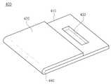
첫째, 상기 지지부재(400)는, 헤밍(Hemming) 가공에 의해 형성된다. 즉, 상기 지지부재(400)는, 도 2 및 도 3에 도시된 바와 같이, 스테인레스와 같은 금속물질 또는 벤딩될 수 있는 합성수지의 일단을 벤딩시키는(굽히는) 공정에 의해, 벤딩된 부분이 라운드지게 형성된다.First, the
둘째, 상기 지지부재(400)는, 상기 디스플레이 패널(100)의 저면에 부착되는 제1지지부(410), 상기 제1지지부(410)로부터 연장되어 라운드지게 형성되어 있으며, 상기 벤딩부(115)와 대면하는 헤밍부(440) 및 상기 헤밍부(440)로부터 연장되어, 상기 제1지지부(410)의 저면에 밀착되어 있는 제2지지부(420)를 포함한다.Second, the
상기 지지부재(400)에서, 상기 제1 기판(110)에 형성되어 있는 상기 벤딩부(115)와 대면하는 상기 헤밍부(440)는 라운드지게 형성되어 있다는 특징을 가지고 있다.In the
상기 지지부재(400)가 금속물질로 형성되면, 상기 지지부재(400)는 상기 디스플레이 패널(100)로부터 발생된 열을 방출시키는 방열기능을 수행할 수도 있다.When the
셋째, 상기 지지부재(400)에는, 상기 패널 구동부(200)를 구성하는 상기 구동 집적 회로(210)가 삽입될 수 있는 구동 집적 회로 홀(430)이 형성되어 있다. 특히, 상기 구동 집적 회로 홀(430)은 상기 제1지지부(410)에 형성될 수 있다. 즉, 상기 패널 구동부(200)가 상기 지지부재(400)의 저면에 밀착되는 경우, 상기 구동 집적 회로(210)가 상기 제1지지부(410)와 직접 닿는 것을 방지하기 위해, 상기 지지부재(400)에는 구동 집적 회로(210)가 삽입될 수 있는 상기 구동 집적 회로 홀(430)이 형성되어 있다.Third, a driving
그러나, 상기 구동 집적 회로 홀(430)은 상기 제2지지부(420)에 형성될 수도 있다. 즉, 상기 제2지지부(420)가 상기 제1지지부(410) 만큼 길게 형성되어, 상기 구동 집적 회로(210)가 상기 제2지지부(420)에 밀착되는 경우, 상기 구동 집적 회로 홀(430)은 상기 제2지지부(420)에 형성될 수 있다.However, the driving
넷째, 도 2 및 도 3에는, 상기 제2지지부(420)의 폭, 즉, 상기 헤밍부(440)로부터, 상기 헤밍부(440)와 마주보고 있는 상기 제2지지부 끝단까지의 길이가, 상기 제1지지부(410)의 폭보다 작게 형성되어 있으나, 본 발명이 이에 한정되는 것은 아니다. 따라서, 상기 제2지지부(420)의 폭은 상기 제1지지부(410)의 폭과 같을 수도 있으며, 클 수도 있다.4 and 3, the width of the
한편, 도 2 및 도 3에는, 상기 제1지지부(410)가 상기 디스플레이 패널(100)의 저면 중 일부만을 지지하고 있는 것으로 도시되어 있으나, 본 발명이 이에 한정되지는 않는다. 즉, 상기 제1지지부(410)는 상기 디스플레이 패널(100)의 저면 전체를 지지할 수 있는 크기로 형성될 수도 있다.2 and 3 illustrate that the
상기 제1지지부(410) 또는 상기 제2지지부(420)에는 상기 구동 집적 회로 홀(430) 이외에도, 상기 패널 구동부(200)에 포함되는 각종 구동소자들이 삽입될 수 있는 적어도 하나의 구동소자홀(미도시)이 형성될 수 있다.At least one driving element hole into which the various driving elements included in the
즉, 상기 구동 집적 회로 홀(430) 또는 상기 구동소자홀(미도시)들은, 상기 구동 집적 회로 또는 상기 구동소자들의 높이가 상기 연성 회로 기판(220)과 상기 지지부재(400) 사이의 간격보다 크게 형성되어, 상기 구동 집적 회로 또는 상기 구동소자들이 상기 지지부재(400)에 직접 접촉되는 것을 방지하기 위한 것이다.That is, the driving
다섯째, 상기 패널 구동부(200)는, 접착부재에 의해 상기 지지부재(400)의 저면에 부착되어 고정될 수 있다.Fifth, the
예를 들어, 상기 패널 구동부(200)가, 상기 벤딩부(115)로부터 연장된 패드부(116)에 연결된 연성 회로 기판(220)과, 상기 연성 회로 기판(220)에 장착되어 있는 구동 집적 회로(210)로 구성된 경우, 상기 제1 기판(110)에 형성되어 있는 상기 패드부(116)와, 상기 연성 회로 기판(220)은, 접착부재에 의해 상기 지지부재(400)의 저면에 부착될 수 있다.For example, the
이 경우, 상기 접착부재는, 상기 패드부(116)에 부착되어, 상기 패드부(116)와 상기 지지부재(400)의 저면 사이에 배치되는 제1접착부재(300) 및 상기 지지부재(400)의 저면에 부착된 상태에서, 상기 연성 회로 기판(220)과 접착되어 있는 제2접착부재(500)를 포함한다.In this case, the adhesive member is attached to the
상기 제1접착부재(300) 및 상기 제2접착부재(500)는, 평판 형상의 플라스틱으로 형성될 수도 있으며, 쿠션을 가지고 있는 다양한 물질로 형성될 수 있다. 쿠션을 가지고 있는 다양한 물질이란, 예를 들어, 라텍스, 스펀지, 발포성 수지인 우레탄 폼, EVA, 실리콘, 또는 쿠션을 가지고 있는 테이프가 될 수 있다.The first
쿠션을 가지고 있는 물질로 형성된 상기 제1접착부재(300) 또는 상기 제2접착부재(500)는, 상기 패드부(116), 상기 연성 회로 기판(220) 또는 상기 구동 집적 회로(210)에 인가되는 충격을 흡수할 수 있다.The first
상기 제1 기판(110)에 형성되어 있는 상기 벤딩부(115)가 상기 지지부재(400)에 형성되어 있는, 상기 헤밍부(440)에 의해 가이드되어 벤딩된 경우, 상기 벤딩부(115)로부터 연장되어 있는 상기 패드부(116)를 상기 지지부재(400)의 저면에 밀착시키기 위해, 상기 제1접착부재(300)가 상기 패드부(116)에 부착된다.When the bending
이 경우, 상기 제1접착부재(300)는 상기 지지부재(400)의 저면에도 부착될 수 있다.In this case, the first
그러나, 상기 제1접착부재(300)가, 상기 제2접착부재(500)보다 단단한 물질로 형성되어 상기 제2접착부재(500)보다 덜 휘는 경우, 예를 들어, 평판 형상의 플라스틱으로 형성되어 있는 경우, 상기 제1접착부재(300)는 상기 패드부(116)에만 부착될 수도 있다. 즉, 평판형태의 상기 제1접착부재(300)에 의해 상기 패드부(116)가 평면을 유지할 수 있기 때문에, 상기 제1접착부재(300)가 상기 지지부재(400)의 저면에 부착되지 않고, 상기 연성 회로 기판(220)만이 상기 지지부재(400)의 저면에 부착될 수도 있다.However, when the first
상기 제1접착부재(300)는 상기 제1 기판(110)의 상기 패드부(116)가 상기 지지부재(400)의 저면에 의해 손상되는 것을 방지할 수도 있다. 즉, 상기 제1 기판(110)은 얇은 막으로 형성되어 있기 때문에, 상기 지지부재(400)의 저면에 생성되어 있는 미세한 돌출부에 의해서도 손상되기 쉽다. 따라서, 상기 지지부재(400)의 저면과 상기 제1 기판(110)의 상기 패드부(116) 사이에 상기 제1접착부재(300)가 삽입됨으로써, 상기한 바와 같은 손상이 방지될 수 있다.The first
또 다른 예로서, 상기 구동 집적 회로(210)가 상기 제1 기판(110)의 상기 패드부(116)에 직접 배치되어 있는 경우, 상기 제1접착부재(300) 또는 상기 제2접착부재(500) 중 어느 하나 만에 의해, 상기 패드부(116)가 상기 지지부재(400)의 저면에 부착될 수도 있다. 이 경우, 상기 패널 구동부(200)를 구성하는 상기 구동 집적 회로(210)는, 상기 접착부재에 의해 상기 패드부(116)가 상기 지지부재(400)의 저면에 부착됨에 따라, 상기 지지부재(400)의 저면에 밀착된 상태로 고정될 수 있다.
As another example, when the driving
도 4는 본 발명에 따른 플렉서블 디스플레이 장치에 적용되는 지지부재를 나타낸 사시도이고, 도 5는 본 발명에 따른 플렉서블 디스플레이 장치에서 벤딩부가 벤딩되지 않은 상태를 나타낸 단면도이며, 도 6은 본 발명에 따른 플렉서블 디스플레이 장치에서 벤딩부가 벤딩되지 않은 상태를 나타낸 저면도이다.4 is a perspective view illustrating a support member applied to a flexible display device according to the present invention, FIG. 5 is a cross-sectional view illustrating a state in which a bending part is not bent in the flexible display device according to the present invention, and FIG. 6 is a flexible view according to the present invention. A bottom view showing a state in which a bending portion is not bent in a display device.
상기에서 설명된 본 발명에 따른 플렉서블 디스플레이 장치의 제조 방법을 설명하면 다음과 같다.The manufacturing method of the flexible display device according to the present invention described above is as follows.
우선, 복수의 화소를 포함하며 일측끝단에 상기 벤딩부(115)가 형성되어 있는 상기 제1 기판(110)과, 상기 제2 기판(120)을 대향 합착시켜 상기 디스플레이 패널(100)을 제조한다.First, the
여기서, 상기 벤딩부(115)로부터 연장되어 있는 상기 패드부(116)에는 상기 패널 구동부(200)가 장착된다. 상기 패널 구동부(200)가 상기 연성 회로 기판(220) 및 상기 구동 집적 회로(210)로 구성된 경우, 상기 패드부(116)에는 상기 연성 회로 기판(220)이 연결되며, 상기 연성 회로 기판(220)에는 상기 구동 집적 회로(210)가 배치되어 있다.The
그러나, 상기 구동 집적 회로(210)는 상기한 바와 같이, 상기 패드부(116)에 직접 배치될 수도 있다.However, the driving
또한, 상기 패드부(116) 중 상기 연성 회로 기판(220) 또는 상기 구동 집적 회로(210)가 배치되어 있지 않은 부분에는, 상기 제1접착부재(300)가 부착된다. 즉, 상기한 바와 같이, 상기 제1접착부재(300)가 플라스틱 재질로 형성된 평판 형태인 경우, 상기 제1접착부재(300)는 상기 패드부(116)에만 부착되어 있을 수도 있다. 이 경우, 상기 패드부(116)가 상기 지지부재(400)의 저면에 배치되더라도, 상기 제1접착부재(300)는 상기 지지부재(400)의 저면에 부착되지 않을 수 있다.In addition, the first
그러나, 상기 제1접착부재(300)의 일측면이 상기 패드부(116)에 부착되어 있는 상태에서, 상기 패드부(116)가 상기 지지부재(400)의 저면에 배치되면, 상기 제1접착부재(300)의 타측면은 지지부재(400)의 저면에 부착될 수도 있다.However, when one side of the first
또한, 상기 제1접착부재(300)는 상기 지지부재(400)의 저면에 배치되어 있다가, 상기 패드부(116)가 상기 지지부재(400)의 저면에 배치되면, 상기 패드부(116)에 부착될 수도 있다.
In addition, the first
다음, 헤밍가공에 의해 라운드진 측면(헤밍부(440))을 갖는 상기 지지부재(400)를 제조한다.Next, the
상기 헤밍가공이란, 상기한 바와 같이, 벤딩된 부분이 라운드지게 형성되는 가공 방법을 말한다.As described above, the hemming process refers to a processing method in which the bent portion is rounded.
상기 지지부재(400)는, 상기 헤밍가공에 의해, 도 4에 도시된 바와 같이, 제1지지부(410), 제2지지부(420) 및 헤밍부(440)를 포함한다. 상기 구동 집적 회로 홀(430)은, 상기 헤밍가공 전에 형성될 수도 있으며, 상기 헤밍가공 이후에 형성될 수도 있다.The
상기 구동 집적 회로 홀(430)은 펀칭 공정에 의해 상기 지지부재(400)에 형성될 수 있다.
The driving
다음, 도 5 및 도 6에 도시된 바와 같이, 상기 디스플레이 패널(100)의 저면에 상기 지지부재(400)를 부착시킨다.Next, as shown in FIGS. 5 and 6, the
이 경우, 상기한 바와 같이, 상기 패드부(116)에는 상기 제1접착부재(300)가 부착되고, 상기 패드부(116)에는 상기 구동 집적 회로(210)가 배치되어 있는 상기 연성 회로 기판(220)이 부착될 수 있으며, 상기 지지부재(400)의 저면에는 상기 제2접착부재(500)가 부착될 수 있다.In this case, as described above, the first
상기 제2접착부재(500)는, 상기 연성 회로 기판(220)에 부착되어 있다가, 상기 지지부재(400)의 저면에 부착될 수도 있다.
The second
다음, 상기 벤딩부(115)를 상기 지지부재(400)의 측면에 형성된 상기 헤밍부(440)를 따라 벤딩시킨다.Next, the bending
상기 헤밍부(440)는 라운드지게 형성되어 있기 때문에, 상기 벤딩부(115)가 벤딩되는 경우, 상기 벤딩부(115)는 라운드지게 형성된다.
Since the hemming
마지막으로, 도 2 및 도 3에 도시된 바와 같이, 상기 벤딩부(115)의 끝단을 상기 지지부재(400)의 저면에 밀착시킨다.Finally, as shown in FIGS. 2 and 3, the end of the bending
즉, 상기 벤딩부(115)로부터 연장되어 있는 상기 패드부(116)는 상기 제1접착부재(300)에 의해 상기 지지부재(400)의 저면에 부착되거나 또는 상기 지지부재(400)의 저면에 밀착된 상태로 배치될 수 있다.That is, the
또한, 상기 벤딩부(115)로부터 연장되어 있는 상기 패드부(116)에 상기 제1접착부재(300)가 부착되어 있는 상태에서, 상기 패드부(116)에 연결되어 있는 상기 연성 회로 기판(220)을 상기 제2접착부재(500)를 이용하여 상기 지지부재(400)의 저면에 부착시킴으로써, 상기 벤딩부(115)의 끝단이 상기 지지부재(400)의 저면에 밀착될 수 있다.In addition, the
이상에서 설명한 본 발명은 전술한 실시 예 및 첨부된 도면에 한정되는 것이 아니고, 본 발명의 기술적 사항을 벗어나지 않는 범위 내에서 여러 가지 치환, 변형 및 변경이 가능하다는 것이 본 발명이 속하는 기술 분야에서 통상의 지식을 가진 자에게 있어 명백할 것이다.The present invention described above is not limited to the above-described embodiments and the accompanying drawings, and it is common in the art that various substitutions, modifications, and changes can be made without departing from the technical matters of the present invention. It will be apparent to those who have the knowledge of.
100 : 디스플레이 패널110 : 제1 기판
120 : 제2기판115 : 벤딩부
116 : 패드부200 : 패널 구동부
210 : 구동 집적 회로220 : 연성 회로 기판
400 : 지지부재410 : 제1지지부
420 : 제2지지부430 : 구동 집적 회로 홀
440 : 헤밍부300 : 제1접착부재
500 : 제2접착부재100: display panel 110: first substrate
120: second substrate 115: bending part
116: pad portion 200: panel drive portion
210: driving integrated circuit 220: flexible circuit board
400: support member 410: first support
420: second support portion 430: driving integrated circuit hole
440: hemming portion 300: the first adhesive member
500: second adhesive member
Claims (10)
Translated fromKorean상기 벤딩부의 끝단에 연결되어 있으며, 상기 화소들로 신호를 공급하는 패널 구동부; 및
상기 제1 기판을 지지하고, 상기 벤딩부의 벤딩을 가이드하도록, 상기 벤딩부와 대면하는 측면이 라운드지게 형성되어 있는 지지부재를 포함하며,
상기 패널 구동부는, 접착부재에 의해 상기 지지부재의 저면에 부착되는 것을 특징으로 하는 플렉서블 디스플레이 장치.A display panel including a first substrate including a plurality of pixels and having a bending portion formed at one end thereof, and a second substrate facing and bonded to the first substrate;
A panel driver connected to an end of the bending part and supplying a signal to the pixels; And
A support member having a rounded side surface facing the bending portion to support the first substrate and guide the bending of the bending portion,
The panel driving unit is attached to the bottom surface of the support member by an adhesive member.
상기 벤딩부의 끝단에 연결되어 있으며, 상기 화소들로 신호를 공급하는 패널 구동부; 및
상기 제1 기판을 지지하고, 상기 벤딩부의 벤딩을 가이드하도록, 상기 벤딩부와 대면하는 측면이 라운드지게 형성되어 있는 지지부재를 포함하며,
상기 패널 구동부는,
상기 벤딩부로부터 연장된 패드부에 연결된 연성 회로 기판; 및
상기 연성 회로 기판에 장착되어 있는 구동 집적 회로를 포함하며,
상기 제1 기판에 형성되어 있는 상기 패드부와, 상기 연성 회로 기판은, 접착부재에 의해 상기 지지부재의 저면에 부착되는 것을 특징으로 하는 플렉서블 디스플레이 장치.A display panel including a first substrate including a plurality of pixels and having a bending portion formed at one end thereof, and a second substrate facing and bonded to the first substrate;
A panel driver connected to an end of the bending part and supplying a signal to the pixels; And
A support member having a rounded side surface facing the bending portion to support the first substrate and guide the bending of the bending portion,
The panel driver,
A flexible circuit board connected to the pad part extending from the bending part; And
A driver integrated circuit mounted to the flexible circuit board,
And the pad portion formed on the first substrate and the flexible circuit board are attached to a bottom surface of the support member by an adhesive member.
상기 접착부재는,
상기 패드부에 부착되어, 상기 패드부와 상기 지지부재의 저면 사이에 배치되는 제1접착부재; 및
상기 지지부재의 저면에 부착된 상태에서, 상기 연성 회로 기판과 접착되어 있는 제2접착부재를 포함하는 플렉서블 디스플레이 장치.The method of claim 3, wherein
The adhesive member,
A first adhesive member attached to the pad part and disposed between the pad part and a bottom surface of the support member; And
And a second adhesive member adhered to the flexible circuit board while being attached to the bottom surface of the support member.
상기 제1접착부재는 상기 제2접착부재보다 덜 휘는 물질로 형성되는 것을 특징으로 하는 플렉서블 디스플레이 장치.The method of claim 4, wherein
The first adhesive member is formed of a material that is less curved than the second adhesive member.
상기 지지부재는,
헤밍가공에 의해 형성되는 것을 특징으로 하는 플렉서블 디스플레이 장치.The method according to any one of claims 2 to 5,
The support member,
Flexible display device, characterized in that formed by hemming.
상기 벤딩부의 끝단에 연결되어 있으며, 상기 화소들로 신호를 공급하는 패널 구동부; 및
상기 제1 기판을 지지하고, 상기 벤딩부의 벤딩을 가이드하도록, 상기 벤딩부와 대면하는 측면이 라운드지게 형성되어 있는 지지부재를 포함하며,
상기 지지부재는,
상기 디스플레이 패널의 저면에 부착되는 제1지지부;
상기 제1지지부로부터 연장되어 라운드지게 형성되어 있으며, 상기 벤딩부와 대면하는 헤밍부; 및
상기 헤밍부로부터 연장되어, 상기 제1지지부의 저면에 밀착되어 있는 제2지지부를 포함하는 플렉서블 디스플레이 장치.A display panel including a first substrate including a plurality of pixels and having a bending portion formed at one end thereof, and a second substrate facing and bonded to the first substrate;
A panel driver connected to an end of the bending part and supplying a signal to the pixels; And
A support member having a rounded side surface facing the bending portion to support the first substrate and guide the bending of the bending portion,
The support member,
A first support part attached to a bottom surface of the display panel;
A hemming part extending from the first support part to be rounded and facing the bending part; And
And a second support portion extending from the hemming portion and in close contact with a bottom surface of the first support portion.
상기 벤딩부의 끝단에 연결되어 있으며, 상기 화소들로 신호를 공급하는 패널 구동부; 및
상기 제1 기판을 지지하고, 상기 벤딩부의 벤딩을 가이드하도록, 상기 벤딩부와 대면하는 측면이 라운드지게 형성되어 있는 지지부재를 포함하며,
상기 지지부재에는,
상기 패널 구동부를 구성하는 구동 집적 회로가 삽입될 수 있는 구동 집적 회로 홀이 형성되어 있는 것을 특징으로 하는 플렉서블 디스플레이 장치.A display panel including a first substrate including a plurality of pixels and having a bending portion formed at one end thereof, and a second substrate facing and bonded to the first substrate;
A panel driver connected to an end of the bending part and supplying a signal to the pixels; And
A support member having a rounded side surface facing the bending portion to support the first substrate and guide the bending of the bending portion,
The support member,
And a driving integrated circuit hole into which a driving integrated circuit constituting the panel driver can be inserted.
헤밍가공에 의해 라운드진 측면을 갖는 지지부재를 제조하는 단계;
상기 디스플레이 패널의 저면에 상기 지지부재를 부착시키는 단계;
상기 벤딩부를 상기 측면을 따라 벤딩시키는 단계; 및
상기 벤딩부의 끝단을 상기 지지부재의 저면에 밀착시키는 단계를 포함하는 플렉서블 디스플레이 장치 제조 방법.Manufacturing a display panel by bonding a first substrate including a plurality of pixels and a bending portion formed at one end thereof, and a second substrate to face each other;
Manufacturing a support member having rounded sides by hemming;
Attaching the support member to a bottom surface of the display panel;
Bending the bending part along the side surface; And
And contacting an end of the bending part with a bottom surface of the support member.
상기 벤딩부의 끝단을 상기 지지부재의 저면에 밀착시키는 단계는,
상기 벤딩부로부터 연장되어 있는 패드부에 제1접착부재가 부착되어 있는 상태에서, 상기 패드부에 연결되어 있는 연성 회로 기판을 제2접착부재를 이용하여 상기 지지부재의 저면에 부착시키는 것을 특징으로 하는 플렉서블 디스플레이 장치 제조 방법.The method of claim 9,
The step of contacting the end of the bending portion to the bottom of the support member,
In a state where the first adhesive member is attached to the pad portion extending from the bending portion, the flexible circuit board connected to the pad portion is attached to the bottom surface of the support member by using the second adhesive member. Flexible display device manufacturing method.
Priority Applications (6)
| Application Number | Priority Date | Filing Date | Title |
|---|---|---|---|
| KR1020130039488AKR102081650B1 (en) | 2013-04-10 | 2013-04-10 | Flexible display device and method of manufacturing the same |
| US14/135,362US9326375B2 (en) | 2013-04-10 | 2013-12-19 | Flexible display device and method of manufacturing the same |
| CN201710055881.0ACN106935146B (en) | 2013-04-10 | 2013-12-20 | Flexible display apparatus |
| CN201310711364.6ACN104103217B (en) | 2013-04-10 | 2013-12-20 | Flexible display device and manufacturing method thereof |
| US15/085,710US9942978B2 (en) | 2013-04-10 | 2016-03-30 | Flexible display device and method of manufacturing the same |
| US15/912,189US10499493B2 (en) | 2013-04-10 | 2018-03-05 | Flexible display device and method of manufacturing the same |
Applications Claiming Priority (1)
| Application Number | Priority Date | Filing Date | Title |
|---|---|---|---|
| KR1020130039488AKR102081650B1 (en) | 2013-04-10 | 2013-04-10 | Flexible display device and method of manufacturing the same |
Publications (2)
| Publication Number | Publication Date |
|---|---|
| KR20140122597A KR20140122597A (en) | 2014-10-20 |
| KR102081650B1true KR102081650B1 (en) | 2020-02-26 |
Family
ID=51671322
Family Applications (1)
| Application Number | Title | Priority Date | Filing Date |
|---|---|---|---|
| KR1020130039488AActiveKR102081650B1 (en) | 2013-04-10 | 2013-04-10 | Flexible display device and method of manufacturing the same |
Country Status (3)
| Country | Link |
|---|---|
| US (3) | US9326375B2 (en) |
| KR (1) | KR102081650B1 (en) |
| CN (2) | CN104103217B (en) |
Families Citing this family (162)
| Publication number | Priority date | Publication date | Assignee | Title |
|---|---|---|---|---|
| KR102042678B1 (en)* | 2013-03-25 | 2019-11-11 | 삼성디스플레이 주식회사 | Display apparatus |
| KR102048467B1 (en)* | 2013-04-03 | 2019-11-26 | 삼성디스플레이 주식회사 | Organic light emitting diode display device |
| KR102081650B1 (en)* | 2013-04-10 | 2020-02-26 | 엘지디스플레이 주식회사 | Flexible display device and method of manufacturing the same |
| KR102095013B1 (en) | 2013-04-11 | 2020-03-31 | 삼성디스플레이 주식회사 | Flexible device |
| KR102079095B1 (en)* | 2013-04-11 | 2020-02-20 | 삼성디스플레이 주식회사 | Display apparatus |
| KR101849339B1 (en)* | 2013-09-30 | 2018-04-17 | 삼성디스플레이 주식회사 | Flexible display device |
| KR102187783B1 (en)* | 2013-12-18 | 2020-12-08 | 삼성디스플레이 주식회사 | Display device |
| TWI582967B (en)* | 2014-04-01 | 2017-05-11 | 鴻海精密工業股份有限公司 | Display array substrate and display array substrate manufacturing method |
| KR102258746B1 (en)* | 2014-08-13 | 2021-06-01 | 삼성전자주식회사 | Chip-on-film package having bending part |
| US9276055B1 (en)* | 2014-08-31 | 2016-03-01 | Lg Display Co., Ltd. | Display device with micro cover layer and manufacturing method for the same |
| KR20190006101A (en) | 2014-10-28 | 2019-01-16 | 가부시키가이샤 한도오따이 에네루기 켄큐쇼 | Light-emitting device and electronic device |
| KR102245101B1 (en)* | 2014-11-13 | 2021-04-27 | 삼성디스플레이 주식회사 | Display device |
| KR20160058329A (en)* | 2014-11-14 | 2016-05-25 | 삼성디스플레이 주식회사 | Flexible display device |
| CN104373855A (en)* | 2014-11-14 | 2015-02-25 | 广东酷柏光电股份有限公司 | Uniformly-luminous LED lamp strip |
| CN106322193A (en)* | 2014-11-14 | 2017-01-11 | 广东酷柏光电股份有限公司 | An energy-saving LED light strip |
| CN106813129A (en)* | 2014-11-14 | 2017-06-09 | 广东酷柏光电股份有限公司 | A kind of LED of energy-conservation |
| US9706607B2 (en)* | 2014-12-10 | 2017-07-11 | Lg Display Co., Ltd. | Flexible display device with multiple types of micro-coating layers |
| US9379355B1 (en)* | 2014-12-15 | 2016-06-28 | Lg Display Co., Ltd. | Flexible display device having support layer with rounded edge |
| US9535522B2 (en)* | 2014-12-22 | 2017-01-03 | Lg Display Co., Ltd. | Flexible organic light emitting diode display device |
| US9490312B2 (en)* | 2014-12-22 | 2016-11-08 | Lg Display Co., Ltd. | Organic light emitting diode display device with flexible printed circuit film |
| KR102350858B1 (en)* | 2014-12-30 | 2022-01-12 | 엘지디스플레이 주식회사 | Display device including flexible substrate |
| JP6448391B2 (en) | 2015-01-28 | 2019-01-09 | 株式会社ジャパンディスプレイ | Display module |
| TWI696108B (en)* | 2015-02-13 | 2020-06-11 | 日商半導體能源研究所股份有限公司 | Functional panel, functional module, light-emitting module, display module, location data input module, light-emitting device, lighting device, display device, data processing device, and manufacturing method of functional panel |
| JP6404150B2 (en)* | 2015-03-12 | 2018-10-10 | 株式会社ジャパンディスプレイ | Manufacturing method of display device |
| JP6404158B2 (en)* | 2015-03-30 | 2018-10-10 | 株式会社ジャパンディスプレイ | Display device |
| KR102312783B1 (en) | 2015-04-06 | 2021-10-15 | 삼성디스플레이 주식회사 | Display device |
| TWI567603B (en)* | 2015-04-16 | 2017-01-21 | Au Optronics Corp | Touch display device |
| KR102415324B1 (en) | 2015-05-04 | 2022-06-30 | 삼성디스플레이 주식회사 | Touch panel and method for manufacturing the same |
| CN104851892A (en)* | 2015-05-12 | 2015-08-19 | 深圳市华星光电技术有限公司 | Narrow frame flexible display device and manufacturing method thereof |
| KR102214353B1 (en)* | 2015-05-29 | 2021-02-10 | 엘지디스플레이 주식회사 | Display Device |
| WO2016194543A1 (en)* | 2015-06-01 | 2016-12-08 | 株式会社ワコム | Position detection sensor and method for manufacturing position detection sensor |
| JP6329925B2 (en) | 2015-06-26 | 2018-05-23 | 株式会社ジャパンディスプレイ | Display device |
| KR102550857B1 (en) | 2015-08-13 | 2023-07-05 | 엘지디스플레이 주식회사 | Flexible display device |
| DE102015113928A1 (en)* | 2015-08-21 | 2017-02-23 | Schreiner Group Gmbh & Co. Kg | Object with an electronic unit and ladder structures on a support structure |
| CN204884440U (en)* | 2015-08-27 | 2015-12-16 | 京东方科技集团股份有限公司 | Flexible display panel and flexible display device |
| KR20170040435A (en)* | 2015-10-02 | 2017-04-13 | 삼성디스플레이 주식회사 | Display device |
| US10001683B2 (en)* | 2015-11-06 | 2018-06-19 | Microsoft Technology Licensing, Llc | Low-profile microdisplay module |
| JP6423781B2 (en)* | 2015-11-20 | 2018-11-14 | 株式会社ジャパンディスプレイ | Display device |
| KR102492104B1 (en)* | 2015-12-10 | 2023-01-27 | 삼성디스플레이 주식회사 | Printed circuit board and display apparatus including the same |
| KR102492454B1 (en)* | 2015-12-11 | 2023-01-27 | 엘지디스플레이 주식회사 | Foldable Display Device |
| KR102432349B1 (en) | 2015-12-15 | 2022-08-16 | 삼성디스플레이 주식회사 | flexible display device |
| CN105448204A (en)* | 2016-01-07 | 2016-03-30 | 友达光电股份有限公司 | Display device |
| KR102398061B1 (en) | 2016-01-11 | 2022-05-16 | 삼성디스플레이 주식회사 | Flexible display apparatus |
| CN106997882B (en)* | 2016-01-26 | 2020-05-22 | 昆山工研院新型平板显示技术中心有限公司 | Bonding structure, flexible screen body with bonding structure and preparation method of flexible screen body |
| JP6423808B2 (en)* | 2016-02-10 | 2018-11-14 | 株式会社ジャパンディスプレイ | Display device |
| KR102577002B1 (en)* | 2016-03-04 | 2023-09-12 | 삼성디스플레이 주식회사 | Apparatus and method for manufacturing the display apparatus |
| KR101821782B1 (en) | 2016-03-11 | 2018-01-25 | 삼성디스플레이 주식회사 | Method for manufacturing display apparatus and display apparatus |
| KR102504128B1 (en) | 2016-03-11 | 2023-02-28 | 삼성디스플레이 주식회사 | Flexible display device |
| KR102659601B1 (en)* | 2016-06-28 | 2024-04-22 | 삼성디스플레이 주식회사 | Display device |
| US10599183B2 (en)* | 2016-06-30 | 2020-03-24 | Intel Corporation | Magnetic shearing solution allowing integrated folding and seamless design for foldable/bendable display form factor devices |
| KR102403197B1 (en) | 2016-07-05 | 2022-05-27 | 삼성디스플레이 주식회사 | Display device |
| KR102732854B1 (en) | 2016-07-13 | 2024-11-21 | 삼성디스플레이 주식회사 | Display device |
| US10919211B2 (en)* | 2016-07-22 | 2021-02-16 | Samsung Display Co., Ltd. | Method of manufacturing display device |
| KR102522358B1 (en)* | 2016-07-22 | 2023-04-18 | 삼성디스플레이 주식회사 | Manufacturing method of display device and apparatus for manufacturing display device |
| CN106066550A (en)* | 2016-07-28 | 2016-11-02 | 武汉华星光电技术有限公司 | Liquid crystal display, display panels and preparation method thereof |
| US10643511B2 (en)* | 2016-08-19 | 2020-05-05 | Apple Inc. | Electronic device display with monitoring circuitry |
| KR102557892B1 (en) | 2016-08-19 | 2023-07-21 | 삼성디스플레이 주식회사 | Display apparatus |
| CN106287343A (en)* | 2016-08-30 | 2017-01-04 | 广东酷柏光电股份有限公司 | A kind of energy-conservation LED |
| KR102650172B1 (en)* | 2016-09-12 | 2024-03-22 | 삼성디스플레이 주식회사 | Display device |
| KR20180030325A (en) | 2016-09-13 | 2018-03-22 | 삼성디스플레이 주식회사 | Display device |
| KR20180032742A (en) | 2016-09-22 | 2018-04-02 | 삼성디스플레이 주식회사 | Flexible display panel and method of bending the same |
| KR102717103B1 (en) | 2016-09-23 | 2024-10-16 | 삼성디스플레이 주식회사 | Display apparatus |
| KR102705336B1 (en) | 2016-10-06 | 2024-09-12 | 삼성디스플레이 주식회사 | Display device |
| JP6199471B1 (en)* | 2016-10-31 | 2017-09-20 | 日本航空電子工業株式会社 | Connector assembly |
| KR20180057773A (en)* | 2016-11-21 | 2018-05-31 | 엘지디스플레이 주식회사 | Display apparatus and manufacturing method for the same |
| KR102604364B1 (en)* | 2016-12-22 | 2023-11-22 | 엘지디스플레이 주식회사 | Flexible display device |
| KR102708773B1 (en) | 2016-12-26 | 2024-09-23 | 엘지디스플레이 주식회사 | Flexible display device |
| KR102773739B1 (en)* | 2016-12-29 | 2025-02-28 | 엘지디스플레이 주식회사 | Flexible Display Device |
| KR102646618B1 (en)* | 2017-01-11 | 2024-03-12 | 삼성디스플레이 주식회사 | Display device and manufacturing method of the same |
| CN106878498A (en)* | 2017-01-22 | 2017-06-20 | 北京小米移动软件有限公司 | Display module and mobile terminal |
| CN106601780A (en)* | 2017-01-24 | 2017-04-26 | 北京小米移动软件有限公司 | Electrical device, display device and preparation method of display device |
| CN106598348A (en)* | 2017-01-24 | 2017-04-26 | 北京小米移动软件有限公司 | Display device and electronic equipment |
| CN106898264B (en)* | 2017-03-06 | 2019-10-22 | 武汉华星光电技术有限公司 | A kind of foldable panel and preparation method thereof |
| CN106910429B (en) | 2017-03-08 | 2019-05-14 | 京东方科技集团股份有限公司 | A kind of flexible die group and preparation method thereof |
| CN108573656A (en) | 2017-03-14 | 2018-09-25 | 昆山工研院新型平板显示技术中心有限公司 | A kind of flexible display screen and flexible display device |
| CN106847871B (en)* | 2017-03-22 | 2020-06-16 | 武汉华星光电技术有限公司 | OLED display panel and display device thereof |
| KR102445445B1 (en)* | 2017-03-28 | 2022-09-21 | 삼성전자주식회사 | A display and an electronic device comprising display |
| KR102357392B1 (en)* | 2017-04-26 | 2022-02-03 | 삼성디스플레이 주식회사 | Display apparatus |
| CN107123617B (en)* | 2017-06-21 | 2020-02-11 | 京东方科技集团股份有限公司 | Display panel, manufacturing method and control method thereof |
| KR102340920B1 (en)* | 2017-06-30 | 2021-12-16 | 엘지디스플레이 주식회사 | Flexible organic light emitting display device and method of manufacturing the same |
| KR102412154B1 (en)* | 2017-07-07 | 2022-06-23 | 삼성디스플레이 주식회사 | Display device and fabricating method of the same |
| KR102370406B1 (en) | 2017-07-10 | 2022-03-07 | 삼성디스플레이 주식회사 | Organic light emitting display device and a method of manufacturing organic light emitting display device |
| CN107221256B (en)* | 2017-07-25 | 2019-04-02 | 武汉华星光电半导体显示技术有限公司 | Flexible Displays component and display screen |
| CN107238958B (en)* | 2017-08-01 | 2024-02-02 | 惠科股份有限公司 | Display panel display device |
| KR102377498B1 (en)* | 2017-09-28 | 2022-03-21 | 엘지디스플레이 주식회사 | Display device |
| US10229963B1 (en)* | 2017-11-01 | 2019-03-12 | Google Llc | Display device including support structure for bending |
| CN107942563B (en)* | 2017-11-28 | 2021-04-30 | 武汉天马微电子有限公司 | Display module and display device |
| KR101899831B1 (en)* | 2017-12-07 | 2018-11-08 | 엘지디스플레이 주식회사 | Flexible display device |
| KR102471758B1 (en)* | 2017-12-11 | 2022-11-29 | 삼성디스플레이 주식회사 | Display device |
| KR102508326B1 (en)* | 2017-12-13 | 2023-03-09 | 삼성디스플레이 주식회사 | Display device |
| KR102581944B1 (en)* | 2017-12-22 | 2023-09-22 | 삼성디스플레이 주식회사 | Display device |
| CN108389876A (en)* | 2018-02-08 | 2018-08-10 | 武汉华星光电半导体显示技术有限公司 | A kind of flexible display panels and flexible display |
| CN108241240B (en)* | 2018-02-08 | 2021-05-14 | 上海天马微电子有限公司 | A display panel and display device |
| US10707289B2 (en) | 2018-02-08 | 2020-07-07 | Wuhan China Star Optoelectronics Semiconductor Display Technology Co., Ltd. | Flexible display panel and flexible display |
| CN108494908B (en)* | 2018-03-09 | 2021-07-23 | Oppo广东移动通信有限公司 | Electronic device and method of manufacture |
| CN111972051A (en)* | 2018-03-16 | 2020-11-20 | 华为技术有限公司 | Assembly and method for electromagnetic interference shielding |
| US11538893B2 (en)* | 2018-03-29 | 2022-12-27 | Sharp Kabushiki Kaisha | Display device |
| CN110501848A (en)* | 2018-05-18 | 2019-11-26 | 胜利仕科技股份有限公司 | Liquid crystal display device |
| CN108682369A (en)* | 2018-05-22 | 2018-10-19 | Oppo广东移动通信有限公司 | Display panel and comprehensive screen display device |
| KR102654593B1 (en) | 2018-06-01 | 2024-04-05 | 삼성디스플레이 주식회사 | Display apparatus and electronic divice including the same |
| KR102601569B1 (en)* | 2018-06-08 | 2023-11-15 | 삼성디스플레이 주식회사 | Display device |
| KR102545950B1 (en)* | 2018-07-12 | 2023-06-23 | 삼성디스플레이 주식회사 | Display device |
| KR102522469B1 (en)* | 2018-07-18 | 2023-04-19 | 삼성디스플레이 주식회사 | Display device |
| CN108962035B (en)* | 2018-08-02 | 2020-11-06 | 京东方科技集团股份有限公司 | Flexible display device |
| JP7148310B2 (en)* | 2018-08-06 | 2022-10-05 | 株式会社ジャパンディスプレイ | Flexible substrate and display device |
| KR102582263B1 (en)* | 2018-08-20 | 2023-09-25 | 삼성디스플레이 주식회사 | Display device and method for manufacturing the same |
| KR102505247B1 (en)* | 2018-09-17 | 2023-02-28 | 엘지디스플레이 주식회사 | Display device |
| JP2020052210A (en)* | 2018-09-26 | 2020-04-02 | 株式会社ジャパンディスプレイ | Display device |
| KR102706503B1 (en)* | 2018-10-08 | 2024-09-12 | 엘지디스플레이 주식회사 | Display Unit |
| CN111240109A (en)* | 2018-11-29 | 2020-06-05 | 北京小米移动软件有限公司 | Display panel, method for producing the same, and display device |
| CN109584713B (en)* | 2018-11-30 | 2020-11-17 | 维沃移动通信有限公司 | Display module and terminal equipment |
| KR102633441B1 (en) | 2018-12-03 | 2024-02-06 | 삼성디스플레이 주식회사 | Display unit, electronic apparatus including the same, and method of manufacturing the electronic apparatus |
| KR102562204B1 (en)* | 2018-12-13 | 2023-07-31 | 엘지디스플레이 주식회사 | Flexible display module and electronic device comprising the same |
| US10642313B1 (en)* | 2018-12-13 | 2020-05-05 | Innolux Corporation | Foldable display device and operation method of electronic device |
| CN109375408A (en)* | 2018-12-17 | 2019-02-22 | 武汉华星光电半导体显示技术有限公司 | A kind of flexible display apparatus |
| JP2020101642A (en)* | 2018-12-20 | 2020-07-02 | シャープ株式会社 | Display device and electronic device |
| KR102644091B1 (en)* | 2018-12-20 | 2024-03-06 | 삼성디스플레이 주식회사 | Display device |
| CN109541834B (en)* | 2018-12-29 | 2021-11-02 | 厦门天马微电子有限公司 | Display panel and display device |
| CN111402725B (en)* | 2019-01-03 | 2022-03-25 | 北京小米移动软件有限公司 | Foldable device and installation method |
| KR20200094885A (en) | 2019-01-30 | 2020-08-10 | 삼성디스플레이 주식회사 | Display device |
| US11116107B2 (en)* | 2019-03-05 | 2021-09-07 | Boe Technology Group Co., Ltd. | Flexible screen |
| TWI872058B (en) | 2019-04-19 | 2025-02-11 | 日商半導體能源研究所股份有限公司 | Flexible member support tool and display device |
| CN109903681B (en) | 2019-04-25 | 2021-09-21 | 京东方科技集团股份有限公司 | Support structure, display device, method of manufacturing the support structure, and method of assembling the display device |
| KR102758915B1 (en)* | 2019-04-25 | 2025-01-24 | 삼성전자주식회사 | Display apparatus |
| CN111853474B (en)* | 2019-04-25 | 2022-02-08 | 三星电子株式会社 | Display device |
| CN110085127B (en)* | 2019-05-23 | 2021-01-26 | 云谷(固安)科技有限公司 | Flexible display mother board and flexible display screen manufacturing method |
| CN110910773B (en)* | 2019-07-26 | 2022-05-24 | 友达光电股份有限公司 | Display device |
| CN110491926B (en) | 2019-08-30 | 2021-11-23 | 京东方科技集团股份有限公司 | Display panel, jig and method for preparing display panel by using jig |
| CN110517593B (en)* | 2019-09-23 | 2022-03-01 | 昆山国显光电有限公司 | Display module and display device |
| US11050030B2 (en) | 2019-09-25 | 2021-06-29 | Wuhan China Star Optoelectronics Semiconductor Display Technology Co., Ltd. | OLED display and OLED display device |
| CN110718159A (en)* | 2019-09-25 | 2020-01-21 | 武汉华星光电半导体显示技术有限公司 | OLED display screen and OLED display device |
| KR20210049326A (en) | 2019-10-25 | 2021-05-06 | 엘지디스플레이 주식회사 | Flexible display device |
| CN112735261A (en)* | 2019-10-28 | 2021-04-30 | 华为技术有限公司 | Flexible display screen and display terminal |
| KR102694298B1 (en)* | 2019-11-04 | 2024-08-12 | 삼성디스플레이 주식회사 | Display panel and display device including the same |
| CN110767092B (en)* | 2019-11-05 | 2021-11-23 | 京东方科技集团股份有限公司 | Display device |
| CN110930881B (en)* | 2019-11-28 | 2021-10-08 | 武汉华星光电半导体显示技术有限公司 | Flexible display module and flexible display device |
| CN210489211U (en)* | 2019-11-29 | 2020-05-08 | 北京京东方显示技术有限公司 | Drive circuit board and display device |
| CN111146189A (en)* | 2019-12-16 | 2020-05-12 | 深圳市华星光电半导体显示技术有限公司 | Display module, preparation method thereof and electronic device |
| KR102823806B1 (en)* | 2019-12-31 | 2025-06-20 | 엘지디스플레이 주식회사 | Display apparatus |
| KR102787589B1 (en)* | 2020-02-18 | 2025-03-28 | 삼성디스플레이 주식회사 | Display device |
| KR102801361B1 (en)* | 2020-03-16 | 2025-05-02 | 삼성디스플레이 주식회사 | Display device |
| KR102845994B1 (en)* | 2020-04-10 | 2025-08-14 | 삼성디스플레이 주식회사 | Display device |
| US11940848B2 (en) | 2020-08-14 | 2024-03-26 | Apple Inc. | Electronic devices with borderless displays |
| CN114120805B (en)* | 2020-08-28 | 2025-03-18 | 京东方科技集团股份有限公司 | Display device, bending gasket module and assembly method thereof |
| CN112071199B (en)* | 2020-09-10 | 2022-06-07 | 武汉华星光电半导体显示技术有限公司 | Display device and electronic apparatus |
| CN114387874A (en)* | 2020-10-21 | 2022-04-22 | 深圳市万普拉斯科技有限公司 | Flexible display panel and mobile terminal |
| CN112289185B (en)* | 2020-10-26 | 2021-11-23 | 武汉华星光电半导体显示技术有限公司 | Display module |
| CN116419958A (en) | 2020-11-05 | 2023-07-11 | 三星电子株式会社 | Electronic device including waterproof structure |
| US12253885B2 (en)* | 2020-12-04 | 2025-03-18 | Samsung Electronics Co., Ltd. | Electronic device including flexible display |
| CN112469193B (en)* | 2020-12-21 | 2022-04-05 | 武汉天马微电子有限公司 | A flexible circuit board assembly and display device |
| KR102819738B1 (en)* | 2020-12-24 | 2025-06-11 | 엘지디스플레이 주식회사 | Display module and display device |
| KR102836941B1 (en) | 2020-12-24 | 2025-07-21 | 엘지디스플레이 주식회사 | Display module and display device |
| CN112634763A (en)* | 2021-01-05 | 2021-04-09 | 武汉华星光电半导体显示技术有限公司 | Display device and terminal equipment |
| CN112599021B (en)* | 2021-01-06 | 2022-08-05 | 武汉华星光电半导体显示技术有限公司 | Display device |
| CN114822234B (en) | 2021-01-29 | 2024-06-14 | 京东方科技集团股份有限公司 | Flexible display module and preparation method thereof |
| CN113066364A (en)* | 2021-03-15 | 2021-07-02 | 武汉华星光电半导体显示技术有限公司 | Flexible display device and preparation method thereof |
| US11538378B1 (en) | 2021-08-17 | 2022-12-27 | International Business Machines Corporation | Digital content adjustment in a flexible display device |
| CN113997679B (en)* | 2021-11-23 | 2024-02-20 | 云谷(固安)科技有限公司 | Bonding device and bonding method |
| JP7293437B1 (en) | 2022-03-11 | 2023-06-19 | レノボ・シンガポール・プライベート・リミテッド | Display assembly and electronics |
| KR102708954B1 (en)* | 2022-04-18 | 2024-09-25 | 주식회사 제이월드 | Radiating sheet for main frame with hinge of a foldable display apparatus |
| US20240397646A1 (en)* | 2022-07-14 | 2024-11-28 | Chengdu Boe Optoelectronics Technology Co., Ltd. | Display panel, splicing screen, and display device |
| CN115762337A (en)* | 2022-10-31 | 2023-03-07 | 京东方科技集团股份有限公司 | Display device and manufacturing method thereof |
Citations (1)
| Publication number | Priority date | Publication date | Assignee | Title |
|---|---|---|---|---|
| KR100995056B1 (en)* | 2008-08-27 | 2010-11-18 | 주식회사 토비스 | LCD display module and terminal equipped with the same |
Family Cites Families (14)
| Publication number | Priority date | Publication date | Assignee | Title |
|---|---|---|---|---|
| JPS56116011A (en)* | 1980-02-18 | 1981-09-11 | Sharp Corp | Liquid crystal display device |
| JP2543281B2 (en)* | 1992-03-02 | 1996-10-16 | 松下電器産業株式会社 | Liquid crystal display panel and display device |
| US5436744A (en)* | 1993-09-03 | 1995-07-25 | Motorola Inc. | Flexible liquid crystal display with integrated driver circuit and display electrodes formed on opposite sides of folded substrate |
| DE19939106A1 (en)* | 1999-08-18 | 2001-04-05 | Infineon Technologies Ag | Ad unit |
| KR100942554B1 (en) | 2008-02-21 | 2010-02-12 | 삼성모바일디스플레이주식회사 | Flat Panel Display |
| US8576209B2 (en) | 2009-07-07 | 2013-11-05 | Semiconductor Energy Laboratory Co., Ltd. | Display device |
| CN101996535A (en) | 2009-08-25 | 2011-03-30 | 精工爱普生株式会社 | Electro-optical device and electronic apparatus |
| JP5507237B2 (en) | 2009-12-25 | 2014-05-28 | 株式会社ジャパンディスプレイ | Liquid crystal display |
| JP5720222B2 (en) | 2010-12-13 | 2015-05-20 | ソニー株式会社 | Display device and electronic device |
| JP2013003171A (en)* | 2011-06-10 | 2013-01-07 | Bridgestone Corp | Information display panel module |
| TWI440939B (en) | 2011-12-30 | 2014-06-11 | Au Optronics Corp | Display device |
| KR102117890B1 (en)* | 2012-12-28 | 2020-06-02 | 엘지디스플레이 주식회사 | Flexible display device and method for manufacturing the same |
| KR102081650B1 (en)* | 2013-04-10 | 2020-02-26 | 엘지디스플레이 주식회사 | Flexible display device and method of manufacturing the same |
| KR102018741B1 (en)* | 2013-06-03 | 2019-09-06 | 삼성디스플레이 주식회사 | Display device with cover window |
- 2013
- 2013-04-10KRKR1020130039488Apatent/KR102081650B1/enactiveActive
- 2013-12-19USUS14/135,362patent/US9326375B2/enactiveActive
- 2013-12-20CNCN201310711364.6Apatent/CN104103217B/enactiveActive
- 2013-12-20CNCN201710055881.0Apatent/CN106935146B/enactiveActive
- 2016
- 2016-03-30USUS15/085,710patent/US9942978B2/enactiveActive
- 2018
- 2018-03-05USUS15/912,189patent/US10499493B2/enactiveActive
Patent Citations (1)
| Publication number | Priority date | Publication date | Assignee | Title |
|---|---|---|---|---|
| KR100995056B1 (en)* | 2008-08-27 | 2010-11-18 | 주식회사 토비스 | LCD display module and terminal equipped with the same |
Also Published As
| Publication number | Publication date |
|---|---|
| CN104103217A (en) | 2014-10-15 |
| CN104103217B (en) | 2017-03-01 |
| US9326375B2 (en) | 2016-04-26 |
| KR20140122597A (en) | 2014-10-20 |
| US9942978B2 (en) | 2018-04-10 |
| US20140307396A1 (en) | 2014-10-16 |
| CN106935146A (en) | 2017-07-07 |
| CN106935146B (en) | 2019-07-09 |
| US10499493B2 (en) | 2019-12-03 |
| US20160210894A1 (en) | 2016-07-21 |
| US20180199426A1 (en) | 2018-07-12 |
Similar Documents
| Publication | Publication Date | Title |
|---|---|---|
| KR102081650B1 (en) | Flexible display device and method of manufacturing the same | |
| US11304294B2 (en) | Display device | |
| KR102037694B1 (en) | Flexible display device and method for manufacturing thereof | |
| KR102009670B1 (en) | Flexible display device and method for manufacturing thereof | |
| KR102200912B1 (en) | Flexible display device and method of manufacturing the same | |
| US9285835B2 (en) | Flexible display device and method of manufacturing the same | |
| KR102033625B1 (en) | Flexible display device and method for manufacturing thereof | |
| KR101956549B1 (en) | Flexible display device and method for manufacturing thereof | |
| KR102233565B1 (en) | Display device | |
| KR102442150B1 (en) | display | |
| KR102283144B1 (en) | Display device | |
| KR102218438B1 (en) | Display device |
Legal Events
| Date | Code | Title | Description |
|---|---|---|---|
| PA0109 | Patent application | Patent event code:PA01091R01D Comment text:Patent Application Patent event date:20130410 | |
| PG1501 | Laying open of application | ||
| A201 | Request for examination | ||
| PA0201 | Request for examination | Patent event code:PA02012R01D Patent event date:20180312 Comment text:Request for Examination of Application Patent event code:PA02011R01I Patent event date:20130410 Comment text:Patent Application | |
| E902 | Notification of reason for refusal | ||
| PE0902 | Notice of grounds for rejection | Comment text:Notification of reason for refusal Patent event date:20190516 Patent event code:PE09021S01D | |
| E701 | Decision to grant or registration of patent right | ||
| PE0701 | Decision of registration | Patent event code:PE07011S01D Comment text:Decision to Grant Registration Patent event date:20191128 | |
| GRNT | Written decision to grant | ||
| PR0701 | Registration of establishment | Comment text:Registration of Establishment Patent event date:20200220 Patent event code:PR07011E01D | |
| PR1002 | Payment of registration fee | Payment date:20200220 End annual number:3 Start annual number:1 | |
| PG1601 | Publication of registration | ||
| PR1001 | Payment of annual fee | Payment date:20230116 Start annual number:4 End annual number:4 | |
| PR1001 | Payment of annual fee | Payment date:20240115 Start annual number:5 End annual number:5 | |
| PR1001 | Payment of annual fee | Payment date:20250115 Start annual number:6 End annual number:6 |