KR102079939B1 - Data storage device and method of scheduling command thereof - Google Patents
Data storage device and method of scheduling command thereofDownload PDFInfo
- Publication number
- KR102079939B1 KR102079939B1KR1020130064069AKR20130064069AKR102079939B1KR 102079939 B1KR102079939 B1KR 102079939B1KR 1020130064069 AKR1020130064069 AKR 1020130064069AKR 20130064069 AKR20130064069 AKR 20130064069AKR 102079939 B1KR102079939 B1KR 102079939B1
- Authority
- KR
- South Korea
- Prior art keywords
- access
- commands
- command
- time
- bank
- Prior art date
- Legal status (The legal status is an assumption and is not a legal conclusion. Google has not performed a legal analysis and makes no representation as to the accuracy of the status listed.)
- Active
Links
Images


Classifications
- G—PHYSICS
- G06—COMPUTING OR CALCULATING; COUNTING
- G06F—ELECTRIC DIGITAL DATA PROCESSING
- G06F9/00—Arrangements for program control, e.g. control units
- G06F9/06—Arrangements for program control, e.g. control units using stored programs, i.e. using an internal store of processing equipment to receive or retain programs
- G06F9/46—Multiprogramming arrangements
- G06F9/48—Program initiating; Program switching, e.g. by interrupt
- G06F9/4806—Task transfer initiation or dispatching
- G06F9/4812—Task transfer initiation or dispatching by interrupt, e.g. masked
- G06F9/4831—Task transfer initiation or dispatching by interrupt, e.g. masked with variable priority
- G06F9/4837—Task transfer initiation or dispatching by interrupt, e.g. masked with variable priority time dependent
- G—PHYSICS
- G06—COMPUTING OR CALCULATING; COUNTING
- G06F—ELECTRIC DIGITAL DATA PROCESSING
- G06F12/00—Accessing, addressing or allocating within memory systems or architectures
- G06F12/02—Addressing or allocation; Relocation
- G06F12/06—Addressing a physical block of locations, e.g. base addressing, module addressing, memory dedication
- G06F12/0646—Configuration or reconfiguration
- G—PHYSICS
- G06—COMPUTING OR CALCULATING; COUNTING
- G06F—ELECTRIC DIGITAL DATA PROCESSING
- G06F13/00—Interconnection of, or transfer of information or other signals between, memories, input/output devices or central processing units
- G06F13/14—Handling requests for interconnection or transfer
- G06F13/16—Handling requests for interconnection or transfer for access to memory bus
- G06F13/18—Handling requests for interconnection or transfer for access to memory bus based on priority control
- G—PHYSICS
- G06—COMPUTING OR CALCULATING; COUNTING
- G06F—ELECTRIC DIGITAL DATA PROCESSING
- G06F3/00—Input arrangements for transferring data to be processed into a form capable of being handled by the computer; Output arrangements for transferring data from processing unit to output unit, e.g. interface arrangements
- G06F3/06—Digital input from, or digital output to, record carriers, e.g. RAID, emulated record carriers or networked record carriers
- G06F3/0601—Interfaces specially adapted for storage systems
- G06F3/0668—Interfaces specially adapted for storage systems adopting a particular infrastructure
- G06F3/0671—In-line storage system
- G06F3/0673—Single storage device
- G06F3/0679—Non-volatile semiconductor memory device, e.g. flash memory, one time programmable memory [OTP]
Landscapes
- Engineering & Computer Science (AREA)
- Theoretical Computer Science (AREA)
- Physics & Mathematics (AREA)
- General Engineering & Computer Science (AREA)
- General Physics & Mathematics (AREA)
- Software Systems (AREA)
- Human Computer Interaction (AREA)
- Information Retrieval, Db Structures And Fs Structures Therefor (AREA)
- Techniques For Improving Reliability Of Storages (AREA)
Abstract
Translated fromKoreanDescription
Translated fromKorean본 발명은 반도체 메모리 장치에 관한 것으로, 좀 더 구체적으로는 데이터 저장 장치 및 그것의 명령어 스케줄링 방법에 관한 것이다.The present invention relates to a semiconductor memory device, and more particularly, to a data storage device and an instruction scheduling method thereof.
반도체 메모리 장치는 크게 휘발성 반도체 메모리 장치(Volatile semiconductor memory device)와 불휘발성 반도체 메모리 장치(Non-volatile semiconductor memory device)로 구분될 수 있다. 휘발성 반도체 메모리 장치는 읽고 쓰는 속도가 빠르지만 전원 공급이 끊기면 저장된 내용이 사라져 버리는 단점이 있다. 반면에 불휘발성 반도체 메모리 장치는 전원 공급이 중단되더라도 그 내용을 보존한다. 그러므로 불휘발성 반도체 메모리 장치는 전원이 공급되었는지의 여부에 관계 없이 보존되어야 할 내용을 기억시키는 데 쓰인다.The semiconductor memory device may be largely classified into a volatile semiconductor memory device and a non-volatile semiconductor memory device. Volatile semiconductor memory devices are fast to read and write, but the stored contents are lost when the power supply is cut off. On the other hand, nonvolatile semiconductor memory devices retain their contents even when their power supplies are interrupted. Therefore, the nonvolatile semiconductor memory device is used to store contents to be preserved regardless of whether or not power is supplied.
불휘발성 반도체 메모리 장치(예를 들면, 플래시 메모리)는 전원의 차단시에도 저장된 데이터를 유지할 수 있기 때문에, 컴퓨터 및 메모리 카드 등에 널리 사용되고 있다. 최근 들어서는, 휴대폰, PDA, 디지털 카메라 등과 같은 모바일 기기의 사용이 급증함에 따라, 하드 디스크 드라이브(HDD) 대신 불휘발성 반도체 메모리 장치가 저장 장치로서 사용되고 있다. 불휘발성 반도체 메모리 장치를 저장 매체로 사용하는 장치를 솔리드 스테이트 드라이브(Solid State Drive) 또는 솔리드 스테이트 디스크(Solid State Disk)라고도 한다. 이하에서는 간단히 SSD라 칭하기로 한다.BACKGROUND ART Nonvolatile semiconductor memory devices (e.g., flash memories) are widely used in computers, memory cards, and the like because they can retain stored data even when power is cut off. In recent years, as the use of mobile devices such as mobile phones, PDAs, digital cameras, and the like is rapidly increasing, nonvolatile semiconductor memory devices are used as storage devices instead of hard disk drives (HDDs). Devices that use nonvolatile semiconductor memory devices as storage media are also referred to as solid state drives or solid state disks. Hereinafter will be referred to simply as SSD.
저전력·대용량화의 추세에 따라 SSD의 저장 매체로 사용되는 불휘발성 메모리 장치는 큰 저장 용량을 제공해야 한다. 저장 용량의 확장을 위하여 SSD에 장착되는 불휘발성 메모리 장치들의 수를 증가시키거나, 대용량의 불휘발성 메모리 장치를 사용할 수 있을 것이다. SSD는 이러한 대용량의 불휘발성 메모리 장치를 효율적으로 관리하기 위하여 멀티 채널 인터리빙(Multi Channel Interleaving) 방식을 사용할 수 있다. 멀티 채널 인터리빙(Multi Channel Interleaving) 방식에 따라 SSD는 불휘발성 메모리 장치를 복수의 채널로 나누어 각각의 채널에서 독립적으로 명령을 수행한다. 멀티 채널 인터리빙(Multi Channel Interleaving) 방식으로 SSD가 가장 효율적으로 운용되기 위해서는 쉬고 있는 채널 없이 모든 채널에서 동작이 수행되고 있어야 할 것이다.With the trend of low power and high capacity, nonvolatile memory devices used as SSD storage media must provide large storage capacity. In order to expand the storage capacity, the number of nonvolatile memory devices mounted in the SSD may be increased, or a large capacity nonvolatile memory device may be used. The SSD may use a multi-channel interleaving scheme to efficiently manage such a large amount of nonvolatile memory devices. According to a multi channel interleaving method, an SSD divides a nonvolatile memory device into a plurality of channels and independently executes commands in each channel. In order for SSDs to operate most efficiently with multi-channel interleaving, operations must be performed on all channels without a resting channel.
본 발명의 목적은 멀티 채널 인터리빙(Multi Channel Interleaving) 방식을 사용하는 데이터 저장 장치의 성능을 향상시키기 위하여 복수의 명령들을 함께 스케줄링 하는 데이터 저장 장치 및 그것의 명령어 스케줄링 방법을 제공하는 데 있다.SUMMARY OF THE INVENTION An object of the present invention is to provide a data storage device for scheduling a plurality of commands together and a command scheduling method thereof in order to improve the performance of a data storage device using a multi channel interleaving scheme.
상기 목적을 달성하기 위한 본 발명에 따른 각각 뱅크 단위로 액세스 되는 복수의 불휘발성 메모리 장치들 및 상기 복수의 불휘발성 메모리 장치들과 복수의 채널들을 통해서 전기적으로 연결되는 메모리 컨트롤러를 포함하는 데이터 저장 장치의 명령어 스케줄링 방법은 액세스 명령들을 상기 뱅크 단위로 상기 복수의 불휘발성 메모리 장치들에 할당하는 단계, 상기 액세스 명령들 각각의 종류를 판별하는 단계, 미리 작성된 정보를 기초로 상기 뱅크에 대하여 유휴 시간 없이 연속적으로 수행될 적어도 2개의 명령들을 결정하는 단계, 그리고 상기 뱅크에 대하여 상기 연속적으로 수행될 적어도 2개의 명령들을 스케줄링 하는 단계를 포함하고, 상기 미리 작성된 정보는 상기 액세스 명령들 각각의 종류에 따라 연속적으로 수행될 명령들의 개수에 대한 정보를 포함한다.According to an aspect of the present invention, there is provided a data storage device including a plurality of nonvolatile memory devices accessed in bank units and a memory controller electrically connected to the plurality of nonvolatile memory devices through a plurality of channels. An instruction scheduling method of the method may further include allocating access commands to the plurality of nonvolatile memory devices on a bank basis, determining a type of each of the access commands, and performing idle time on the bank based on previously written information. Determining at least two instructions to be executed in succession, and scheduling at least two instructions to be executed in succession for the bank, wherein the pre-written information is contiguous in accordance with the type of each of the access instructions. For the number of commands to be executed Contains information.
또한, 본 발명에 따른 각각 뱅크 단위로 액세스 되는 복수의 불휘발성 메모리 장치들 및 상기 복수의 불휘발성 메모리 장치들과 복수의 채널들을 통해서 전기적으로 연결되는 메모리 컨트롤러를 포함하는 데이터 저장 장치의 명령어 스케줄링 방법은 액세스 명령들을 상기 뱅크 단위로 상기 복수의 불휘발성 메모리 장치들에 할당하는 단계, 상기 액세스 명령들 각각의 수행 시간을 계산하는 단계, 상기 액세스 명령들의 수행 시간 합계와 오버헤드 시간을 비교하여 상기 뱅크에 대하여 유휴 시간 없이 연속적으로 수행될 적어도 2개의 명령들을 결정하는 단계, 그리고 상기 뱅크에 대하여 상기 연속적으로 수행될 적어도 2개의 명령들을 스케줄링 하는 단계를 포함한다.In addition, the command scheduling method of a data storage device including a plurality of nonvolatile memory devices each accessed in a bank unit and a memory controller electrically connected to the plurality of nonvolatile memory devices through a plurality of channels according to the present invention. Allocating access commands to the plurality of nonvolatile memory devices in the bank unit, calculating an execution time of each of the access commands, and comparing an execution time sum of the access commands with an overhead time. Determining at least two instructions to be executed in succession without idle time for, and scheduling the at least two instructions to be executed in succession for the bank.
또한, 본 발명에 따른 데이터 저장 장치는 각각 뱅크 단위로 액세스 되는 복수의 불휘발성 메모리 장치들, 그리고 상기 복수의 불휘발성 메모리 장치들과 복수의 채널들을 통해서 전기적으로 연결되며, 액세스 명령들을 상기 뱅크 단위로 할당하는 메모리 컨트롤러를 포함하되, 상기 메모리 컨트롤러는 상기 액세스 명령들의 종류를 판별하고, 미리 작성된 정보에 기초하여 상기 뱅크에 대하여 유휴 시간 없이 연속적으로 수행될 적어도 2개의 명령들을 스케줄링 하고, 상기 미리 작성된 정보는 상기 액세스 명령들의 종류에 따라 상기 연속적으로 수행될 적어도 2개의 명령들의 개수에 대한 정보를 포함한다.In addition, the data storage device according to the present invention is electrically connected to each of a plurality of nonvolatile memory devices that are accessed in units of banks, and to the plurality of nonvolatile memory devices through a plurality of channels. And a memory controller, wherein the memory controller determines a type of the access instructions, schedules at least two instructions to be successively executed without idle time for the bank, based on previously prepared information, and The information includes information on the number of the at least two commands to be executed sequentially according to the type of the access commands.
이상과 같은 본 발명의 실시 예에 따르면, 데이터 저장 장치의 각 채널에서 수행 시간이 오버헤드 시간(Overhead Time)보다 짧은 복수의 명령들을 함께 스케줄링 하여 각 채널의 유휴 시간(Idle Time)을 최소화하는 데이터 저장 장치 및 그것의 명령어 스케줄링 방법을 제공할 수 있다.According to the embodiment of the present invention as described above, data for minimizing idle time of each channel by scheduling a plurality of commands whose execution time is shorter than the overhead time in each channel of the data storage device. A storage device and its command scheduling method can be provided.
도 1은 본 발명의 실시 예에 따른 데이터 저장 장치를 보여주는 구성도이다.
도 2는 도 1의 메모리 컨트롤러를 자세히 보여주는 구성도이다.
도 3은 도 2의 플래시 인터페이스와 연결되는 복수의 플래시 메모리들을 자세히 보여주는 구성도이다.
도 4a는 도 1의 데이터 저장 장치의 명령 수행 과정을 보여주는 타이밍도이다.
도 4b는 도 1의 데이터 저장 장치의 다른 명령 수행 과정을 보여주는 타이밍도이다.
도 5는 본 발명의 실시 예에 따른 데이터 저장 장치의 제어 방법을 보여주는 순서도이다.
도 6은 본 발명의 다른 실시 예에 따른 데이터 저장 장치의 제어 방법을 보여주는 순서도이다.1 is a block diagram illustrating a data storage device according to an embodiment of the present invention.
FIG. 2 is a detailed block diagram illustrating the memory controller of FIG. 1.
FIG. 3 is a detailed diagram illustrating a plurality of flash memories connected to the flash interface of FIG. 2.
4A is a timing diagram illustrating a command execution process of the data storage device of FIG. 1.
4B is a timing diagram illustrating another command execution process of the data storage device of FIG. 1.
5 is a flowchart illustrating a control method of a data storage device according to an embodiment of the present invention.
6 is a flowchart illustrating a control method of a data storage device according to another exemplary embodiment.
앞의 일반적인 설명 및 다음의 상세한 설명 모두 예시적이라는 것이 이해되어야 하며, 청구된 발명의 부가적인 설명이 제공되는 것으로 여겨져야 한다. 참조부호들이 본 발명의 바람직한 실시 예들에 상세히 표시되어 있으며, 그것의 예들이 참조 도면들에 표시되어 있다. 가능한 어떤 경우에도, 동일한 참조 번호들이 동일한 또는 유사한 부분을 참조하기 위해서 설명 및 도면들에 사용된다.It is to be understood that both the foregoing general description and the following detailed description are exemplary, and that additional explanations of the claimed invention are provided. Reference numerals are indicated in detail in the preferred embodiments of the present invention, examples of which are indicated in the reference figures. In any case, like reference numerals are used in the description and drawings to refer to the same or similar parts.
이하에서는, 플래시 메모리(Flash Memory)가 본 발명의 특징 및 기능을 설명하기 위한 저장 장치 또는 전자 장치의 한 예로서 사용될 것이다. 하지만, 이 기술 분야에 정통한 사람은 여기에 기재된 내용에 따라 본 발명의 다른 이점들 및 성능을 쉽게 이해할 수 있을 것이다. 또한, 본 발명은 다른 실시 예들을 통해 구현되거나 적용될 수 있을 것이다. 게다가, 상세한 설명은 본 발명의 범위, 기술적 사상 그리고 다른 목적으로부터 상당히 벗어나지 않고, 관점 및 응용에 따라 수정되거나 변경될 수 있다.In the following, a flash memory will be used as an example of a storage device or an electronic device for explaining the features and functions of the present invention. However, one of ordinary skill in the art will readily appreciate the other advantages and performances of the present invention in accordance with the teachings herein. In addition, the present invention may be implemented or applied through other embodiments. In addition, the detailed description may be modified or changed according to aspects and applications without departing from the scope, spirit and other objects of the present invention.
도 1은 본 발명의 실시 예에 따른 데이터 저장 장치를 보여주는 구성도이다. 도 1을 참조하면, 데이터 저장 장치(100)는 메모리의 동작을 전반적으로 제어하는 메모리 컨트롤러(110), 송수신 되는 데이터를 임시로 저장하는 버퍼 메모리(120) 및 복수의 채널을 통하여 메모리 컨트롤러(110)와 전기적으로 연결되는 저장 매체(130)를 포함한다. 예를 들어, 데이터 저장 장치(100)는 멀티 채널 인터리빙(Multi Channel Interleaving) 방식을 사용하는 SSD, 메모리 카드 등 다양한 저장 장치들을 포함할 수 있다.1 is a block diagram illustrating a data storage device according to an embodiment of the present invention. Referring to FIG. 1, the
메모리 컨트롤러(110)는 호스트(Host)로부터 복수의 명령들을 수신한다. 호스트(Host)로부터 수신되는 명령들은 저장 매체(130)에 접근해야 하는 액세스 명령(Access Command)들을 포함한다. 예를 들어, 액세스 명령(Access Command)은 읽기(Read) 또는 쓰기(Write) 명령 등을 포함한다. 액세스 명령(Access Command)들을 수신하면, 메모리 컨트롤러(110)는 액세스 명령(Access Command)들을 채널별(CH1~CHn)로 할당한다. 메모리 컨트롤러(110)는 각 채널(CH1~CHn)에 할당된 명령들을 스케줄링 한다. 각 채널(CH1~CHn)에서 스케줄링 된 명령들은 스케줄링 순서에 따라 독립적으로 수행된다.The
버퍼 메모리(120)는 호스트(Host)로부터 수신되는 데이터 또는 호스트(Host)로 전송되는 데이터를 임시로 저장한다. 버퍼 메모리(120)는 휘발성 메모리(예를 들면 SRAM 또는 DRAM)로 구현될 수 있다. 또한, 버퍼 메모리(120)는 데이터를 임시로 저장할 수 있는 어떠한 장치로도 구현될 수 있다.The
저장 매체(130)는 불휘발성 메모리 장치를 포함한다. 이하에서 저장 매체(130)는 플래시 메모리(Flash Memory)로 구성되는 경우에 대해 예시적으로 설명될 것이다. 그러나 본 발명의 저장 매체(130)에 적용되는 불휘발성 메모리 장치는 특정 종류 및 특정 형태에만 국한되지 않고 다양한 형태로 구성될 수 있다. 예를 들면, 저장 매체(130)에 적용되는 불휘발성 메모리 장치는 플래시 메모리(Flash Memory)뿐만 아니라 MRAM, PRAM 등의 불휘발성 메모리를 포함할 수 있다.The
저장 매체(130)는 복수의 플래시 메모리(Flash Memory)들을 포함한다. 제 1 플래시 메모리들(131)은 제 1 채널(CH1)을 통하여 메모리 컨트롤러(110)와 연결된다. 제 2 플래시 메모리들(132)은 제 2 채널(CH2)을 통하여 메모리 컨트롤러(110)와 연결된다. 제 n 플래시 메모리들(133)은 제 n 채널(CHn)을 통하여 메모리 컨트롤러(110)와 연결된다. 각 채널(CH1~CHn)의 플래시 메모리들(131~133)은 스케줄링 순서에 따라 독립적으로 스케줄링 된 명령들을 수행한다.The
도 2는 도 1의 메모리 컨트롤러를 자세히 보여주는 구성도이다. 도 2를 참조하면, 메모리 컨트롤러(110)는 프로세싱 유닛(111), 동작 메모리(112), 호스트 인터페이스(113), 버퍼 인터페이스(114) 및 플래시 인터페이스(115)를 포함할 수 있다. 하지만, 메모리 컨트롤러(110)의 구성 요소들이 언급된 구성 요소들에 국한되지 않음은 잘 이해될 것이다. 예를 들면, 메모리 컨트롤러(110)는 초기 부팅 동작에 필요한 코드 데이터를 저장하는 ROM, 손상된 데이터를 복구하는 에러 정정 유닛(ECC) 등이 더 포함될 수 있다.FIG. 2 is a detailed block diagram illustrating the memory controller of FIG. 1. Referring to FIG. 2, the
프로세싱 유닛(111)은 중앙 처리 장치(CPU) 또는 마이크로프로세서(Microprocessor)를 포함한다. 프로세싱 유닛(111)은 메모리 컨트롤러(110)의 동작을 전반적으로 제어한다. 프로세싱 유닛(111)은 메모리 컨트롤러(110)를 제어하기 위한 펌웨어(Firmware)를 구동하도록 구성된다. 이러한 펌웨어(Firmware)는 동작 메모리(112)에 로딩 되어 구동된다. 프로세싱 유닛(111)은 호스트(Host)로부터 수신된 액세스 명령(Access Command)들을 각 채널(CH1~CHn)에 할당한다.The
동작 메모리(112)에는 메모리 컨트롤러(110)를 제어하기 위한 펌웨어(Firmware) 및 데이터가 저장된다. 저장된 펌웨어(Firmware) 및 데이터는 프로세싱 유닛(111)에 의해 구동된다. 동작 메모리(112)는 캐시(Cache), DRAM, SRAM, PRAM, ROM, 플래시 메모리 장치들 중 적어도 하나를 포함한다. 동작 메모리(112)에는 펌웨어(Firmware)인 명령 스케줄러(Command Scheduler)가 로딩 되어 구동된다.The operating
명령 스케줄러(Command Scheduler)는 프로세싱 유닛(111)에 의해 각 채널(CH1~CHn)에 할당된 명령들을 채널별(CH1~CHn)로 스케줄링 한다. 명령 스케줄러(Command Scheduler)는 각 채널(CH1~CHn)에 할당된 명령들의 수행 시간(Operation time) 및 리소스(Resource, 예를 들어 명령 대기 큐의 메모리 용량)의 크기를 고려하여 한번에 스케줄링 될 명령들의 개수를 결정한다. 이에 관하여는 도 3에서 자세히 설명될 것이다.The command scheduler schedules commands allocated to each of the channels CH1 to CHn by the
호스트 인터페이스(113)는 호스트(Host)와 메모리 컨트롤러(110) 사이의 인터페이스를 제공한다. 호스트(Host)와 메모리 컨트롤러(110)는 다양한 표준 인터페이스들 중 하나를 통해 연결될 수 있다. 또는 호스트(Host)와 메모리 컨트롤러(110)는 다양한 표준 인터페이스들 중 복수의 인터페이스들을 통해 연결될 수 있다. 여기에서, 표준 인터페이스들은 ATA(Advanced Technology Attachment), SATA(Serial ATA), e-SATA(external SATA), SCSI(Small Computer Small Interface), SAS(Serial Attached SCSI), PCI(Peripheral Component Interconnection), PCI-E(PCI Express), USB(Universal Serial Bus), IEEE 1394, NVMe(Non-volatile Memory Express), Card 인터페이스 등과 같은 다양한 인터페이스 방식들을 포함한다.The
버퍼 인터페이스(114)는 프로세싱 유닛(111)의 제어에 응답해서 버퍼 메모리(120, 도 1 참조)의 액세스 동작(예를 들면, 읽기/기록/소거 동작들)을 제어한다. 버퍼 메모리(120)는 휘발성 메모리(예를 들면, SRAM 또는 DRAM)로 구현될 수 있다. 버퍼 메모리(120)는 저장 매체(130)와 호스트(Host) 사이에서 전달되는 데이터를 임시적으로 저장하는 기능을 수행한다.The
플래시 인터페이스(115)는 복수의 플래시 메모리들(131∼133)과 복수의 채널들(CH1∼CHn)을 통해 데이터를 주고받는다. 각 채널(CH1∼CHn)에는 복수의 플래시 메모리들(131~133)이 전기적으로 연결될 수 있다. 플래시 인터페이스(115)는 각 채널(CH1~CHn)에 연결되는 명령 대기 큐(Command Waiting Queue)들을 포함한다. 명령 스케줄러(Command Scheduler)는 각 채널(CH1~CHn)에 할당된 명령들을 각 채널(CH1~CHn)의 명령 대기 큐(Command Waiting Queue)에 스케줄링 한다. 스케줄링 된 명령들은 각 채널(CH1~CHn)의 복수의 플래시 메모리들(131~133)에서 독립적으로 수행된다.The
도 3은 도 2의 플래시 인터페이스와 연결되는 복수의 플래시 메모리들을 자세히 보여주는 구성도이다. 도 3을 참조하면, 플래시 인터페이스(115)는 복수의 명령 대기 큐들(Queue 1~Queue n)을 포함한다. 복수의 명령 대기 큐들(Queue 1~Queue n)은 복수의 채널들(CH1~CHn)을 통해서 복수의 플래시 메모리들(131~133)과 연결된다.FIG. 3 is a detailed diagram illustrating a plurality of flash memories connected to the flash interface of FIG. 2. Referring to FIG. 3, the
복수의 명령 대기 큐들(Queue 1~Queue n)은 휘발성 메모리(예를 들면, SRAM 또는 DRAM)로 구현될 수 있다. 복수의 명령 대기 큐들(Queue 1~Queue n)은 각 채널(CH1~CHn)과 독립적으로 연결된다. 제 1 명령 대기 큐(Queue 1)는 제 1 채널(CH1)을 통하여 제 1 플래시 메모리들(131)과 연결된다. 제 2 명령 대기 큐(Queue 2)는 제 2 채널(CH2)을 통하여 제 2 플래시 메모리들(132)과 연결된다. 제 n 명령 대기 큐(Queue n)는 제 n 채널(CHn)을 통하여 제 n 플래시 메모리들(133)과 연결된다. 복수의 명령 대기 큐들(Queue 1~Queue n)에는 스케줄링 되는 명령들 및 그와 관련된 정보들이 저장된다.The plurality of command
복수의 플래시 메모리들(131~133)은 복수의 뱅크들(Bank 1~Bank m)을 포함할 수 있다. 본 발명에서 뱅크(Bank)는 하나의 채널 내에서 명령들을 인터리빙(Interleaving)하여 동작하는 단위를 말한다. 하나의 뱅크(Bank)는 하나의 플래시 메모리(Flash Memory)로 구현될 수 있고, 또는 복수의 플래시 메모리(Flash Memory)들로 구현될 수도 있다.The
프로세싱 유닛(111, 도 2 참조)은 호스트(Host)로부터 수신된 액세스 명령(Access Command)들을 각 채널(CH1~CHn)에 할당한다. 각 채널(CH1~CHn)에 명령들이 할당될 때, 명령들의 수행될 채널 및 뱅크(Bank)가 결정된다. 명령 스케줄러(Command Scheduler)는 할당된 명령들을 채널별(CH1~CHn)로 스케줄링 한다. 예를 들면, 명령 스케줄러(Command Scheduler)는 제 1 채널(CH1)을 선택한다. 명령 스케줄러(Command Scheduler)는 제 1 플래시 메모리들(131)의 제 1 뱅크(Bank 1)에서 수행될 첫 번째 명령부터 제 m 뱅크(Bank m)에서 수행될 첫 번째 명령까지를 제 1 명령 대기 큐(Queue 1)에 스케줄링 한다. 제 1 채널(CH1)의 첫 번째 명령들에 대한 스케줄링이 완료되면, 명령 스케줄러(Command Scheduler)는 제 2 채널(CH2)을 선택한다. 명령 스케줄러(Command Scheduler)는 제 2 플래시 메모리들(132)의 뱅크들(Bank 1~Bank m)에서 수행될 첫 번째 명령들을 제 1 채널(CH1)과 같은 방법으로 제 2 명령 대기 큐(Queue 2)에 스케줄링 한다. 이와 같은 방법으로 제 n 채널(CHn)까지 각 뱅크(Bank)에서 수행될 첫 번째 명령들이 스케줄링 된 후, 명령 스케줄러(Command Scheduler)는 제 1 명령 대기 큐(Queue 1)에 첫 번째 명령들과 같은 방법으로 두 번째 명령들을 스케줄링 한다. 각 채널(CH1~CHn)의 명령 대기 큐(Queue 1~Queue n)에 스케줄링 된 명령들은 스케줄링 순서에 따라 각 채널(CH1~CHn)의 각 뱅크(Bank 1~Bank m)에서 독립적으로 수행된다.The processing unit 111 (refer to FIG. 2) allocates access commands received from the host to each channel CH1 to CHn. When instructions are assigned to each channel CH1 to CHn, the channel and bank to be executed of the instructions are determined. The command scheduler schedules the allocated commands for each channel CH1 to CHn. For example, the command scheduler selects the first channel CH1. The command scheduler queues the first command to be executed in the
이상의 스케줄링 방법에 따르면 제 1 명령 대기 큐(Queue 1)에 스케줄링 될 두 번째 명령들은 모든 채널들(CH1~CHn)에서 첫 번째 명령들의 스케줄링이 완료된 이후에 스케줄링 될 수 있다. 만약 제 1 채널(CH1)의 제 1 뱅크(Bank 1)에서 수행된 첫 번째 명령의 수행 시간이 너무 짧은 경우, 제 1 채널(CH1)의 제 1 뱅크(Bank 1)에 두 번째 명령이 수행되기 전에 첫 번째 명령은 완료될 수 있다. 그러면 제 1 채널(CH1)의 제 1 뱅크(Bank 1)는 두 번째 명령이 수행될 때까지 동작을 쉬게 된다. 멀티 채널 인터리빙(Multi Channel Interleaving) 방식을 사용하는 경우, 각 채널(CH1~CHn)의 각 뱅크(Bank)에서 이러한 유휴 시간(Idle Time)이 증가할수록 데이터 저장 장치(100)의 성능은 떨어지게 된다.According to the above scheduling method, the second commands to be scheduled in the first command
따라서, 본 발명의 실시 예에 따른 명령 스케줄러(Command Scheduler)는 각 채널(CH1~CHn)의 각 뱅크(Bank 1~Bank m)에서 수행될 복수의 명령들을 함께 스케줄링 할 수 있다. 이하에서 하나의 뱅크(Bank)에서 수행될 첫 번째 명령이 명령 대기 큐(Command Waiting Queue)에 스케줄링 된 후 두 번째 명령이 스케줄링 되기까지 걸리는 시간을 오버헤드 시간(Overhead Time)이라 정의하기로 한다. 오버헤드 시간(Overhead Time)은 채널 및 뱅크(Bank)의 개수에 따라 일정한 값으로 정해질 수 있다. 명령 스케줄러(Command Scheduler)는 함께 스케줄링 될 명령들의 수행 시간 합계와 오버헤드 시간(Overhead Time)을 비교하여 함께 스케줄링 될 명령들의 개수를 정할 수 있다. 예를 들면, 명령들은 그 종류에 따라 평균 수행 시간의 예측이 가능할 것이다. 명령의 종류에 따른 평균 수행 시간에 따라 함께 스케줄링 될 명령들의 개수가 미리 정해질 수 있다. 명령 스케줄러(Command Scheduler)는 미리 정해진 개수에 따라 복수의 명령들을 함께 스케줄링 할 수 있다. 또는, 명령 스케줄러(Command Scheduler)는 채널에 할당된 명령들의 수행 시간을 계산하여 스케줄링 할 때마다 스케줄링 될 명령들의 개수를 결정할 수 있다. 자세한 내용은 도 5 및 도 6에서 설명될 것이다.Accordingly, the command scheduler according to an embodiment of the present invention may schedule a plurality of commands to be performed in each
이상의 본 발명에 따른 명령 스케줄링(Command Scheduling) 방법에 따르면 각 뱅크(Bank)의 유휴 시간(Idle Time)은 줄어들게 된다. 유휴 시간(Idle Time)이 감소하면 데이터 저장 장치(100)의 성능은 향상될 수 있다. 다만, 한번에 스케줄링 되는 명령들의 개수는 명령 대기 큐(Queue 1~Queue n)의 리소스(Resource) 크기에 의해 제한될 수 있다.According to the command scheduling method according to the present invention, the idle time of each bank is reduced. When the idle time is reduced, the performance of the
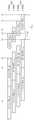
도 4a 및 도 4b는 본 발명에 따른 명령 스케줄링(Command Scheduling) 방법의 효과를 설명하기 위한 도면이다. 이하에서는 도 1 내지 도 3을 참조하여 설명할 것이다. 도 4a 및 도 4b에서 데이터 저장 장치(100)는 예시적으로 2개의 채널들(CH1, CH2)을 포함한다고 가정할 것이다. 또한, 각 채널(CH1, CH2)은 2개의 뱅크들(Bank 1, Bank 2)을 포함한다고 가정할 것이다. 하지만, 이것은 설명을 위한 가정일 뿐, 데이터 저장 장치(100)는 복수의 채널들 및 각 채널에 포함되는 복수의 뱅크(Bank)들을 포함할 수 있다. t1 내지 t8의 값은 도 4a와 도 4b에서 다를 수 있다.4A and 4B are diagrams for explaining the effects of a command scheduling method according to the present invention. Hereinafter, a description will be given with reference to FIGS. 1 to 3. 4A and 4B, it will be assumed that the
도 4a는 도 1의 데이터 저장 장치의 명령 수행 과정을 보여주는 타이밍도이다. 메모리 컨트롤러(110)에 포함된 명령 스케줄러(Command Scheduler)는 명령 대기 큐들(Queue 1, Queue 2)에 모든 뱅크(Bank)들에서 수행될 명령들을 순차적으로 스케줄링 한다. 도 4a를 참조하면, t1 시점에 제 1 채널(CH1)의 제 1 뱅크(Bank 1)에서 수행될 첫 번째 명령은 스케줄링 되고 수행되기 시작한다. 첫 번째 명령은 t1 시점부터 제 1 수행 시간(First Operation Time) 후인 t3 시점에 완료된다. 도 4a에서 데이터 저장 장치(100)의 오버헤드 시간(Overhead Time)은 ΔTOH(t5-t1)이다. 결국, 제 1 채널(CH1)의 제 1 뱅크(Bank 1)에서 유휴 시간(Idle Time, ΔTidle)이 존재하게 된다. 나머지 뱅크(Bank)들에서도 역시 유휴 시간(Idle Time)이 존재할 수 있다. 각 뱅크(Bank)에서 유휴 시간(Idle Time)이 길어질수록 데이터 저장 장치(100)의 성능은 떨어질 것이다. 만약에 채널 및 뱅크(Bank)의 개수가 늘어나면 오버헤드 시간(Overhead Time)은 더 길어질 것이다. 오버헤드 시간(Overhead Time)이 길어지면 유휴 시간(Idle Time)도 길어질 것이다.4A is a timing diagram illustrating a command execution process of a data storage device of FIG. 1. The command scheduler included in the
t5 시점에 제 1 채널(CH1)의 제 1 뱅크(Bank 1)에서 수행될 두 번째 명령은 스케줄링 되고 수행되기 시작한다. 두 번째 명령은 t5 시점부터 제 2 수행 시간(Second Operation Time) 후인 t7 시점에 완료된다. 제 2 수행 시간(Second Operation Time)은 ΔTOH보다 길다. 따라서 세 번째 명령은 t7 시점보다 이전에 스케줄링 된다(스케줄링 시점은 미도시). 세 번째 명령은 두 번째 명령이 완료되는 t7 시점에 바로 수행되기 시작할 수 있다. 그러므로 제 2 수행 시간(Second Operation Time)과 제 3 수행 시간(Third Operation Time) 사이에는 유휴 시간(Idle Time)이 없다. 결국, 명령 수행 시간이 오버헤드 시간(Overhead Time)보다 길게 되면, 각 뱅크(Bank)에서 유휴 시간(Idle Time)이 없을 수 있다.At a time t5, a second command to be performed in the
도 4b는 도 1의 데이터 저장 장치의 다른 명령 수행 과정을 보여주는 타이밍도이다. 도 4b를 참조하면, t1 시점에 제 1 채널(CH1)의 제 1 뱅크(Bank 1)에서 수행될 첫 번째 및 두 번째 명령이 함께 스케줄링 되고, 첫 번째 명령은 수행되기 시작한다. t3 시점에 첫 번째 명령은 완료되고, 바로 두 번째 명령이 수행되기 시작한다. t1 시점부터 오버헤드 시간(Overhead Time)이 지난 후인 t5 시점에 세 번째 명령은 스케줄링 된다. t7 시점에 두 번째 명령은 완료되고, 유휴 시간(Idle Time) 없이 세 번째 명령은 수행되기 시작한다. 나머지 뱅크(Bank)들에서도 첫 번째 및 두 번째 명령이 함께 스케줄링 된다. 이와 같이 함께 스케줄링 되는 명령들의 수행 시간 총합이 오버헤드 시간(Overhead Time)보다 길도록 복수의 명령들이 함께 스케줄링 되면, 각 채널(CH1, CH2)의 각 뱅크(Bank 1, Bank 2)에서 유휴 시간(Idle Time)은 줄어들게 된다. 유휴 시간(Idle Time)이 감소하면, 데이터 저장 장치(100)의 성능은 향상될 것이다.4B is a timing diagram illustrating another command execution process of the data storage device of FIG. 1. Referring to FIG. 4B, at the time t1, the first and second commands to be performed in the
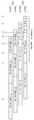
도 5는 본 발명의 실시 예에 따른 데이터 저장 장치의 제어 방법을 보여주는 순서도이다. 이하에서는 도 1 내지 도 3을 참조하여 설명한다. 도 5를 참조하면, 명령의 종류에 따라 미리 정해진 개수의 명령들을 함께 스케줄링 하는 방법이 설명된다.5 is a flowchart illustrating a control method of a data storage device according to an embodiment of the present invention. Hereinafter, a description will be given with reference to FIGS. 1 to 3. Referring to FIG. 5, a method of scheduling a predetermined number of commands together according to the type of commands will be described.
S110 단계에서, 메모리 컨트롤러(110)는 호스트(Host)로부터 액세스 명령(Access Command)들을 수신한다. 예를 들면, 액세스 명령(Access Command)들은 읽기(Read) 또는 쓰기(Write) 명령 등과 같이 저장 매체(130)에 접근을 요하는 명령들을 포함한다.In operation S110, the
S120 단계에서, 메모리 컨트롤러(110)는 수신된 액세스 명령(Access Command)들을 각 채널(CH1~CHn)에 할당한다. 할당된 명령들은 수행될 채널 및 뱅크(Bank)가 정해진다.In operation S120, the
S130 단계에서, 액세스 명령(Access Command)들이 각 채널(CH1~CHn)에 할당된 후, 메모리 컨트롤러(110)는 할당된 명령들을 스케줄링 하기 위해서 채널들(CH1~CHn) 중에서 하나의 채널을 선택한다. 예를 들면, 메모리 컨트롤러(110)는 제 1 채널(CH1)을 선택할 수 있다.In operation S130, after access commands are allocated to each of the channels CH1 to CHn, the
S140 단계에서, 메모리 컨트롤러(110)는 선택된 채널에 할당된 명령들의 종류를 판별한다. 일반적으로 명령의 종류가 같으면 명령의 수행 시간도 일정한 범위 안에 존재할 것이다. 따라서, 명령의 종류에 따른 평균 수행 시간에 따라 미리 함께 스케줄링 될 명령들의 개수는 정해질 수 있다. 메모리 컨트롤러(110)는 미리 정해진 함께 스케줄링 될 명령들의 개수를 룩업 테이블(Look-up Table)로 저장할 수 있다.In operation S140, the
S150 단계에서, 메모리 컨트롤러(110)는 선택된 채널에 할당된 명령들의 종류에 따라 스케줄링 될 명령들의 개수를 결정한다. 메모리 컨트롤러(110)는 미리 정해진 표(Table)에 따라 함께 스케줄링 될 명령들의 개수를 결정한다. 함께 스케줄링 될 명령들의 개수는 선택된 채널의 각 뱅크(Bank 1~Bank m)마다 독립적으로 결정된다. 그러므로 선택된 채널의 각 뱅크(Bank 1~Bank m)마다 함께 스케줄링 될 명령들의 개수는 다를 수 있다. 다만, 함께 스케줄링 되는 명령들의 개수는 명령 대기 큐(Command Waiting Queue)의 리소스(Resource) 크기에 의해 제한된다.In operation S150, the
S160 단계에서, 메모리 컨트롤러(110)는 선택된 채널에 스케줄링 결정된 명령들을 함께 스케줄링 한다. 선택된 채널의 스케줄링이 완료되면, 메모리 컨트롤러(110)는 다음에 스케줄링 될 채널을 선택한다. 이상의 방법으로 메모리 컨트롤러(110)는 호스트(Host)로부터 수신된 모든 액세스 명령(Access Command)들이 스케줄링 될 때까지 각 채널(CH1~CHn)에 할당된 명령들을 계속 스케줄링 한다.In operation S160, the
도 6은 본 발명의 다른 실시 예에 따른 데이터 저장 장치의 제어 방법을 보여주는 순서도이다. 이하에서는 도 1 내지 도 3을 참조하여 설명한다. 도 6을 참조하면, 각 채널(CH1~CHn)에 할당된 명령들의 수행 시간을 계산하고, 함께 스케줄링 될 명령들의 수행 시간 합계와 오버헤드 시간(Overhead Time)을 비교하여 복수의 명령들을 함께 스케줄링 하는 방법이 설명된다.6 is a flowchart illustrating a control method of a data storage device according to another exemplary embodiment. Hereinafter, a description will be given with reference to FIGS. 1 to 3. Referring to FIG. 6, the execution time of the commands allocated to each channel CH1 to CHn is calculated, and the execution time of the commands to be scheduled together is compared with the overhead time to schedule the plurality of commands together. The method is described.
S210 단계에서, 메모리 컨트롤러(110)는 호스트(Host)로부터 액세스 명령(Access Command)들을 수신한다. 예를 들면, 액세스 명령(Access Command)들은 읽기(Read) 또는 쓰기(Write) 명령 등과 같이 저장 매체(130)에 접근을 요하는 명령들을 포함한다.In operation S210, the
S220 단계에서, 메모리 컨트롤러(110)는 수신된 액세스 명령(Access Command)들을 각 채널(CH1~CHn)에 할당한다. 할당된 명령들은 수행될 채널 및 뱅크(Bank)가 정해진다.In operation S220, the
S230 단계에서, 액세스 명령(Access Command)들이 각 채널(CH1~CHn)에 할당된 후, 메모리 컨트롤러(110)는 할당된 명령들을 스케줄링 하기 위해서 채널들(CH1~CHn) 중에서 하나의 채널을 선택한다. 예를 들면, 메모리 컨트롤러(110)는 제 1 채널(CH1)을 선택할 수 있다.In operation S230, after access commands are allocated to each of the channels CH1 to CHn, the
S240 단계에서, 메모리 컨트롤러(110)는 선택된 채널에 할당된 각 명령의 수행 시간을 계산한다. 메모리 컨트롤러(110)는 스케줄링 될 첫 번째 명령부터 순차적으로 수행 시간을 합하면서 오버헤드 시간(Overhead Time)과 비교한다. 예를 들면, 메모리 컨트롤러(110)는 첫 번째 명령의 수행 시간과 오버헤드 시간(Overhead Time)을 비교한다. 첫 번째 명령의 수행 시간이 오버헤드 시간(Overhead Time)보다 작으면, 메모리 컨트롤러(110)는 첫 번째 및 두 번째 명령의 수행 시간 합계와 오버헤드 시간(Overhead Time)을 비교한다. 첫 번째 및 두 번째 명령의 수행 시간 합계가 오버헤드 시간(Overhead Time)보다 작으면, 메모리 컨트롤러(110)는 첫 번째, 두 번째 및 세 번째 명령의 수행 시간 합계와 오버헤드 시간(Overhead Time)을 비교한다. 이와 같은 방법으로 메모리 컨트롤러(110)는 스케줄링 될 명령들의 수행 시간 합계가 오버헤드 시간(Overhead Time)보다 크거나 같을 때까지 반복하여 비교한다.In operation S240, the
S250 단계에서, 메모리 컨트롤러(110)는 선택된 채널에 스케줄링 될 명령들의 수행 시간 합계에 따라 스케줄링 되는 명령들의 개수를 결정한다. 메모리 컨트롤러(110)는 스케줄링 될 명령들의 수행 시간 합계가 오버헤드 시간(Overhead Time)보다 크거나 같을 때의 명령들의 개수를 함께 스케줄링 되는 명령들의 개수로 결정한다. 예를 들면, 첫 번째 명령의 수행 시간이 오버헤드 시간(Overhead Time)보다 크거나 같으면, 메모리 컨트롤러(110)는 첫 번째 명령만 스케줄링 한다. 첫 번째 명령의 수행 시간은 오버헤드 시간(Overhead Time)보다 작으나 첫 번째 및 두 번째 명령의 수행 시간 합계가 오버헤드 시간(Overhead Time)보다 크거나 같으면, 메모리 컨트롤러(110)는 첫 번째 및 두 번째 명령을 함께 스케줄링 한다. 첫 번째 및 두 번째 명령의 수행 시간 합계가 오버헤드 시간(Overhead Time)보다 작으나 첫 번째, 두 번째 및 세 번째 명령의 수행 시간 합계가 오버헤드 시간(Overhead Time)보다 크거나 같으면, 메모리 컨트롤러(110)는 첫 번째, 두 번째 및 세 번째 명령을 함께 스케줄링 한다. 다만, 함께 스케줄링 되는 명령들의 개수는 명령 대기 큐(Command Waiting Queue)의 리소스(Resource) 크기에 의해 제한된다.In operation S250, the
S260 단계에서, 메모리 컨트롤러(110)는 선택된 채널에 결정된 명령들을 함께 스케줄링 한다. 선택된 채널의 스케줄링이 완료되면, 메모리 컨트롤러(110)는 다음에 스케줄링 될 채널을 선택한다. 이상의 방법으로 메모리 컨트롤러(110)는 호스트(Host)로부터 수신된 모든 액세스 명령(Access Command)들이 스케줄링 될 때까지 각 채널(CH1~CHn)에 할당된 명령들을 계속 스케줄링 한다.In operation S260, the
도 5 및 도 6에서 설명한 본 발명의 실시 예에 따르면 데이터 저장 장치(100)는 각 채널의 각 뱅크(Bank)에서 유휴 시간(Idle Time)을 최소한으로 줄일 수 있다. 결국, 전반적으로 유휴 시간(Idle Time)이 감소하여 데이터 저장 장치(100)의 성능은 향상될 수 있다. 그리고 이상에서 살펴본 복수의 명령들을 스케줄링 하는 방법은 예시적인 것이고, 함께 스케줄링 될 명령들의 개수를 결정하는 방법은 이상의 실시 예에 의해 한정되지 않는다.According to the exemplary embodiments described with reference to FIGS. 5 and 6, the
본 발명에 따른 저장 매체 그리고/또는 메모리 컨트롤러는 다양한 형태들의 패키지를 이용하여 실장 될 수 있다. 예를 들면, 본 발명에 따른 저장 매체 그리고/또는 메모리 컨트롤러는 PoP(Package on Package), Ball grid arrays(BGAs), Chip scale packages(CSPs), Plastic Leaded Chip Carrier(PLCC), Plastic Dual In-Line Package(PDIP), Die in Waffle Pack, Die in Wafer Form, Chip On Board(COB), Ceramic Dual In-Line Package(CERDIP), Plastic Metric Quad Flat Pack(MQFP), Thin Quad Flatpack(TQFP), Small Outline(SOIC), Shrink Small Outline Package(SSOP), Thin Small Outline(TSOP), System In Package(SIP), Multi Chip Package(MCP), Wafer-level Fabricated Package(WFP), Wafer-Level Processed Stack Package(WSP), 등과 같은 패키지들을 이용하여 실장 될 수 있다.The storage medium and / or memory controller according to the present invention may be mounted using various types of packages. For example, the storage medium and / or memory controller according to the present invention may be a package on package (PoP), ball grid arrays (BGAs), chip scale packages (CSPs), plastic leaded chip carrier (PLCC), plastic dual in-line Package (PDIP), Die in Waffle Pack, Die in Wafer Form, Chip On Board (COB), Ceramic Dual In-Line Package (CERDIP), Plastic Metric Quad Flat Pack (MQFP), Thin Quad Flatpack (TQFP), Small Outline (SOIC), Shrink Small Outline Package (SSOP), Thin Small Outline (TSOP), System In Package (SIP), Multi Chip Package (MCP), Wafer-level Fabricated Package (WFP), Wafer-Level Processed Stack Package (WSP) Can be implemented using packages such as
이상에서와 같이 도면과 명세서에서 최적 실시 예가 개시되었다. 여기서 특정한 용어들이 사용되었으나, 이는 단지 본 발명을 설명하기 위한 목적에서 사용된 것이지 의미 한정이나 특허청구범위에 기재된 본 발명의 범위를 제한하기 위하여 사용된 것은 아니다. 그러므로 본 기술 분야의 통상의 지식을 가진 자라면 이로부터 다양한 변형 및 균등한 타 실시 예가 가능하다는 점을 이해할 것이다. 따라서, 본 발명의 진정한 기술적 보호 범위는 첨부된 특허청구범위의 기술적 사상에 의해 정해져야 할 것이다.As described above, optimal embodiments have been disclosed in the drawings and the specification. Although specific terms have been used herein, they are used only for the purpose of describing the present invention and are not used to limit the scope of the present invention as defined in the meaning or claims. Therefore, those skilled in the art will understand that various modifications and equivalent other embodiments are possible. Therefore, the true technical protection scope of the present invention will be defined by the technical spirit of the appended claims.
100 : 데이터 저장 장치
110 : 메모리 컨트롤러
111 : 프로세싱 유닛
112 : 동작 메모리
113 : 호스트 인터페이스
114 : 버퍼 인터페이스
115 : 플래시 인터페이스
120 : 버퍼 메모리
130 : 저장 매체
131 : 제 1 복수의 플래시 메모리들
132 : 제 2 복수의 플래시 메모리들
133 : 제 n 복수의 플래시 메모리들100: data storage device
110: memory controller
111: processing unit
112: operation memory
113: host interface
114: buffer interface
115: flash interface
120: buffer memory
130: storage medium
131: first plurality of flash memories
132: second plurality of flash memories
133: nth plurality of flash memories
Claims (8)
Translated fromKorean액세스 명령들을 상기 불휘발성 메모리 장치에 할당하는 단계;
상기 액세스 명령들 각각의 종류들을 판별하는 단계;
미리 작성된 정보를 기초로 상기 복수의 뱅크들 중 제 1 뱅크에 대하여 유휴 시간 없이 연속적으로 수행될 적어도 2개의 액세스 명령들을 결정하는 단계; 그리고
상기 제 1 뱅크에 대하여 상기 유휴 시간 없이 상기 연속적으로 수행될 적어도 2개의 액세스 명령들을 스케줄링 하는 단계를 포함하되,
상기 미리 작성된 정보는 상기 액세스 명령들 각각의 상기 종류들에 따라 연속적으로 수행될 액세스 명령들의 개수에 대한 정보를 포함하고, 그리고
상기 개수는 상기 명령 대기 큐의 리소스 크기를 고려하여 결정되는 명령어 스케줄링 방법.A method of scheduling a data storage device, the method comprising: a nonvolatile memory device including a plurality of banks, and a memory controller including a command wait queue electrically connected to the nonvolatile memory device;
Assigning access commands to the nonvolatile memory device;
Determining types of each of the access instructions;
Determining at least two access commands to be successively performed without idle time for a first one of the plurality of banks based on previously written information; And
Scheduling at least two access instructions to be executed sequentially without said idle time for said first bank,
The pre-written information includes information on the number of access commands to be executed consecutively according to the kinds of each of the access commands, and
The number is determined by taking into account the resource size of the command waiting queue.
상기 미리 작성된 정보를 기초로 상기 복수의 뱅크들 중 제 2 뱅크에 대하여 상기 유휴 시간 없이 연속적으로 수행될 적어도 2개의 액세스 명령들을 결정하는 단계를 더 포함하되,
상기 제 2 뱅크에 대하여 상기 유휴 시간 없이 상기 연속적으로 수행될 적어도 2개의 액세스 명령들의 개수는 상기 제 1 뱅크에 대하여 상기 유휴 시간 없이 상기 연속적으로 수행될 적어도 2개의 액세스 명령들의 개수와는 상이한 명령어 스케줄링 방법.The method of claim 1,
Determining at least two access commands to be executed consecutively without the idle time for a second one of the plurality of banks based on the pre-written information;
The number of at least two access commands to be executed sequentially without the idle time for the second bank is different from the number of at least two access commands to be executed consecutively without the idle time for the first bank. Way.
상기 미리 작성된 정보는 룩업 테이블로 제공되는 명령어 스케줄링 방법.The method of claim 1,
And the pre-written information is provided as a lookup table.
액세스 명령들을 상기 불휘발성 메모리 장치에 할당하는 단계;
상기 액세스 명령들 각각의 수행 시간들을 계산하는 단계;
상기 액세스 명령들 중 일부 액세스 명령들의 수행 시간 합계가 오버헤드 시간보다 큰 경우, 상기 복수의 뱅크들 중 제 1 뱅크에 대하여 유휴 시간 없이 연속적으로 수행될 적어도 2개의 명령들로서 상기 일부 액세스 명령들을 결정하는 단계; 그리고
상기 제 1 뱅크에 대하여 상기 유휴 시간 없이 상기 연속적으로 수행될 적어도 2개의 액세스 명령들을 스케줄링 하는 단계를 포함하는 명령어 스케줄링 방법.A method of scheduling instructions of a data storage device, the method comprising: a nonvolatile memory device including a plurality of banks, and a memory controller electrically connected to the nonvolatile memory device;
Assigning access commands to the nonvolatile memory device;
Calculating execution times of each of the access instructions;
If the sum of execution times of some of the access commands is greater than an overhead time, determining the some access commands as at least two commands to be executed continuously without idle time for a first bank of the plurality of banks; step; And
Scheduling at least two access instructions to be executed sequentially without said idle time for said first bank.
상기 오버헤드 시간은 상기 제 1 뱅크에 대하여 제 1 액세스 명령을 스케줄링 한 후에 제 2 액세스 명령을 스케줄링 할 때까지의 시간인 명령어 스케줄링 방법.The method of claim 4, wherein
Wherein the overhead time is a time from scheduling a first access command to scheduling a second access command for the first bank.
제 1 수행 시간 합계는 제 1 액세스 명령의 수행 시간과 제 2 액세스 명령의 수행 시간을 합하여 계산되고, 그리고
상기 제 1 수행 시간 합계가 상기 오버헤드 시간보다 큰 경우, 상기 연속적으로 수행될 적어도 2개의 액세스 명령들은 상기 제 1 액세스 명령 및 상기 제 2 액세스 명령으로 결정되는 명령어 스케줄링 방법.The method of claim 4, wherein
The first execution time sum is calculated by summing the execution time of the first access command with the execution time of the second access command, and
And when the first execution time sum is greater than the overhead time, the at least two access commands to be executed in succession are determined by the first access command and the second access command.
상기 제 1 수행 시간 합계가 상기 오버헤드 시간보다 작은 경우, 제 2 수행 시간 합계는 상기 제 1 수행 시간 합계와 제 3 액세스 명령의 수행 시간을 합하여 계산되고, 그리고
상기 제 2 수행 시간 합계가 상기 오버헤드 시간보다 큰 경우, 상기 연속적으로 수행될 적어도 2개의 액세스 명령들은 상기 제 1 액세스 명령, 상기 제 2 액세스 명령, 및 상기 제 3 액세스 명령으로 결정되는 명령어 스케줄링 방법.The method of claim 6,
If the first execution time sum is less than the overhead time, the second execution time sum is calculated by adding the execution time of the first execution time sum and the third access command, and
When the second execution time sum is greater than the overhead time, the at least two access commands to be executed in succession are determined by the first access command, the second access command, and the third access command. .
상기 복수의 불휘발성 메모리 장치들과 각각 전기적으로 연결되는 복수의 명령 대기 큐들을 포함하고, 그리고 액세스 명령들을 상기 복수의 불휘발성 메모리 장치들 각각의 상기 복수의 뱅크들에 할당하는 메모리 컨트롤러를 포함하되,
상기 메모리 컨트롤러는 상기 액세스 명령들의 종류들을 판별하고, 미리 작성된 정보에 기초하여 상기 복수의 뱅크들 중 제 1 뱅크에 대하여 유휴 시간 없이 연속적으로 수행될 적어도 2개의 액세스 명령들을 스케줄링 하고, 그리고
상기 미리 작성된 정보는 상기 액세스 명령들의 상기 종류들에 따라 상기 연속적으로 수행될 적어도 2개의 액세스 명령들의 개수에 대한 정보를 포함하되, 상기 개수는 상기 복수의 명령 대기 큐들의 리소스 크기들을 고려하여 결정되는 데이터 저장 장치.A plurality of nonvolatile memory devices each comprising a plurality of banks; And
A memory controller including a plurality of command wait queues each electrically connected to the plurality of nonvolatile memory devices, and allocating access commands to the plurality of banks of each of the plurality of nonvolatile memory devices. ,
The memory controller determines types of the access commands, schedules at least two access commands to be successively executed without idle time for a first one of the plurality of banks based on previously written information, and
The pre-written information includes information on the number of at least two access commands to be executed sequentially according to the types of the access commands, the number being determined in consideration of the resource sizes of the plurality of command wait queues. Data storage.
Priority Applications (1)
| Application Number | Priority Date | Filing Date | Title |
|---|---|---|---|
| KR1020130064069AKR102079939B1 (en) | 2013-06-04 | 2013-06-04 | Data storage device and method of scheduling command thereof |
Applications Claiming Priority (1)
| Application Number | Priority Date | Filing Date | Title |
|---|---|---|---|
| KR1020130064069AKR102079939B1 (en) | 2013-06-04 | 2013-06-04 | Data storage device and method of scheduling command thereof |
Publications (2)
| Publication Number | Publication Date |
|---|---|
| KR20140142530A KR20140142530A (en) | 2014-12-12 |
| KR102079939B1true KR102079939B1 (en) | 2020-02-21 |
Family
ID=52459993
Family Applications (1)
| Application Number | Title | Priority Date | Filing Date |
|---|---|---|---|
| KR1020130064069AActiveKR102079939B1 (en) | 2013-06-04 | 2013-06-04 | Data storage device and method of scheduling command thereof |
Country Status (1)
| Country | Link |
|---|---|
| KR (1) | KR102079939B1 (en) |
Cited By (2)
| Publication number | Priority date | Publication date | Assignee | Title |
|---|---|---|---|---|
| WO2022256067A1 (en)* | 2021-06-02 | 2022-12-08 | Intel Corporation | Double fetch for long burst length memory data transfer |
| US11880601B2 (en) | 2021-05-20 | 2024-01-23 | SK Hynix Inc. | Data storage device for performing read operation and operating method thereof |
Families Citing this family (6)
| Publication number | Priority date | Publication date | Assignee | Title |
|---|---|---|---|---|
| US9477408B1 (en)* | 2015-04-14 | 2016-10-25 | Samsung Electronics Co., Ltd. | Memory systems having improved out-of-order execution of commands and methods for operating the same |
| US10275160B2 (en) | 2015-12-21 | 2019-04-30 | Intel Corporation | Method and apparatus to enable individual non volatile memory express (NVME) input/output (IO) Queues on differing network addresses of an NVME controller |
| US10200376B2 (en) | 2016-08-24 | 2019-02-05 | Intel Corporation | Computer product, method, and system to dynamically provide discovery services for host nodes of target systems and storage resources in a network |
| US10176116B2 (en) | 2016-09-28 | 2019-01-08 | Intel Corporation | Computer product, method, and system to provide discovery services to discover target storage resources and register a configuration of virtual target storage resources mapping to the target storage resources and an access control list of host nodes allowed to access the virtual target storage resources |
| KR102518884B1 (en)* | 2017-12-20 | 2023-04-07 | 에스케이하이닉스 주식회사 | Memory system and operating method thereof |
| US11669272B2 (en)* | 2019-05-31 | 2023-06-06 | Micron Technology, Inc. | Predictive data transfer based on availability of media units in memory sub-systems |
Citations (2)
| Publication number | Priority date | Publication date | Assignee | Title |
|---|---|---|---|---|
| JP3223530B2 (en) | 1991-08-20 | 2001-10-29 | 富士通株式会社 | Data transfer instruction generation processing method |
| JP2004110786A (en) | 2002-09-16 | 2004-04-08 | Arm Ltd | Data processor and data processing method |
Family Cites Families (3)
| Publication number | Priority date | Publication date | Assignee | Title |
|---|---|---|---|---|
| EP2071468A4 (en)* | 2006-12-25 | 2010-11-03 | Panasonic Corp | MEMORY CONTROL DEVICE, MEMORY DEVICE, AND MEMORY CONTROL METHOD |
| KR20100042885A (en)* | 2008-10-17 | 2010-04-27 | 삼성전자주식회사 | How Nonvolatile Memory Devices Work |
| KR101679359B1 (en)* | 2010-05-27 | 2016-11-25 | 삼성전자 주식회사 | Controlling Method for non-volatile memory device |
- 2013
- 2013-06-04KRKR1020130064069Apatent/KR102079939B1/enactiveActive
Patent Citations (2)
| Publication number | Priority date | Publication date | Assignee | Title |
|---|---|---|---|---|
| JP3223530B2 (en) | 1991-08-20 | 2001-10-29 | 富士通株式会社 | Data transfer instruction generation processing method |
| JP2004110786A (en) | 2002-09-16 | 2004-04-08 | Arm Ltd | Data processor and data processing method |
Cited By (3)
| Publication number | Priority date | Publication date | Assignee | Title |
|---|---|---|---|---|
| US11880601B2 (en) | 2021-05-20 | 2024-01-23 | SK Hynix Inc. | Data storage device for performing read operation and operating method thereof |
| WO2022256067A1 (en)* | 2021-06-02 | 2022-12-08 | Intel Corporation | Double fetch for long burst length memory data transfer |
| US12321634B2 (en) | 2021-06-02 | 2025-06-03 | Intel Corporation | Double fetch for long burst length memory data transfer |
Also Published As
| Publication number | Publication date |
|---|---|
| KR20140142530A (en) | 2014-12-12 |
Similar Documents
| Publication | Publication Date | Title |
|---|---|---|
| KR102079939B1 (en) | Data storage device and method of scheduling command thereof | |
| US11561914B2 (en) | Storage device and interrupt generation method thereof | |
| US8171242B2 (en) | Systems and methods for scheduling a memory command for execution based on a history of previously executed memory commands | |
| US9711232B2 (en) | Dynamic non-volatile memory operation scheduling for controlling power consumption of solid-state drives | |
| CN106067321B (en) | Controller suitable for memory programming pause-resume | |
| US9977487B2 (en) | Dynamic non-volatile memory operation scheduling for controlling power consumption of solid-state drives | |
| US10782915B2 (en) | Device controller that schedules memory access to a host memory, and storage device including the same | |
| US8555000B2 (en) | Data storage device and data storing method thereof | |
| US8458394B2 (en) | Storage device and method of managing a buffer memory of the storage device | |
| US8356135B2 (en) | Memory device and control method | |
| CN109697027B (en) | Data storage device including shared memory region and dedicated memory region | |
| KR101687762B1 (en) | Storage device and command scheduling method thereof | |
| US20150205540A1 (en) | Memory system including nonvolatile memory devices and operating method | |
| US8621140B2 (en) | Flash memory apparatus for controlling operation in response to generation of interrupt signal and method of controlling the same | |
| US20100125697A1 (en) | Computing device having storage, apparatus and method of managing storage, and file system recorded recording medium | |
| US20160378375A1 (en) | Memory system and method of operating the same | |
| KR20100120518A (en) | Data storage device and read commands execution method thereof | |
| US10310746B2 (en) | Method, associated memory device and controller thereof for performing dynamic resource management | |
| US9460005B2 (en) | Storage devices including memory device and methods of operating the same | |
| US9208076B2 (en) | Nonvolatile storage device and method of storing data thereof |
Legal Events
| Date | Code | Title | Description |
|---|---|---|---|
| PA0109 | Patent application | Patent event code:PA01091R01D Comment text:Patent Application Patent event date:20130604 | |
| PG1501 | Laying open of application | ||
| PA0201 | Request for examination | Patent event code:PA02012R01D Patent event date:20180601 Comment text:Request for Examination of Application Patent event code:PA02011R01I Patent event date:20130604 Comment text:Patent Application | |
| E902 | Notification of reason for refusal | ||
| PE0902 | Notice of grounds for rejection | Comment text:Notification of reason for refusal Patent event date:20190530 Patent event code:PE09021S01D | |
| E701 | Decision to grant or registration of patent right | ||
| PE0701 | Decision of registration | Patent event code:PE07011S01D Comment text:Decision to Grant Registration Patent event date:20191121 | |
| GRNT | Written decision to grant | ||
| PR0701 | Registration of establishment | Comment text:Registration of Establishment Patent event date:20200217 Patent event code:PR07011E01D | |
| PR1002 | Payment of registration fee | Payment date:20200218 End annual number:3 Start annual number:1 | |
| PG1601 | Publication of registration | ||
| PR1001 | Payment of annual fee | Payment date:20240125 Start annual number:5 End annual number:5 |