KR102077794B1 - Organic light emitting diode display device and method for aging the same - Google Patents
Organic light emitting diode display device and method for aging the sameDownload PDFInfo
- Publication number
- KR102077794B1 KR102077794B1KR1020130132751AKR20130132751AKR102077794B1KR 102077794 B1KR102077794 B1KR 102077794B1KR 1020130132751 AKR1020130132751 AKR 1020130132751AKR 20130132751 AKR20130132751 AKR 20130132751AKR 102077794 B1KR102077794 B1KR 102077794B1
- Authority
- KR
- South Korea
- Prior art keywords
- light emitting
- organic light
- power supply
- voltage line
- supply voltage
- Prior art date
- Legal status (The legal status is an assumption and is not a legal conclusion. Google has not performed a legal analysis and makes no representation as to the accuracy of the status listed.)
- Expired - Fee Related
Links
Images


Classifications
- G—PHYSICS
- G09—EDUCATION; CRYPTOGRAPHY; DISPLAY; ADVERTISING; SEALS
- G09G—ARRANGEMENTS OR CIRCUITS FOR CONTROL OF INDICATING DEVICES USING STATIC MEANS TO PRESENT VARIABLE INFORMATION
- G09G3/00—Control arrangements or circuits, of interest only in connection with visual indicators other than cathode-ray tubes
- G09G3/20—Control arrangements or circuits, of interest only in connection with visual indicators other than cathode-ray tubes for presentation of an assembly of a number of characters, e.g. a page, by composing the assembly by combination of individual elements arranged in a matrix no fixed position being assigned to or needed to be assigned to the individual characters or partial characters
- G09G3/22—Control arrangements or circuits, of interest only in connection with visual indicators other than cathode-ray tubes for presentation of an assembly of a number of characters, e.g. a page, by composing the assembly by combination of individual elements arranged in a matrix no fixed position being assigned to or needed to be assigned to the individual characters or partial characters using controlled light sources
- G09G3/30—Control arrangements or circuits, of interest only in connection with visual indicators other than cathode-ray tubes for presentation of an assembly of a number of characters, e.g. a page, by composing the assembly by combination of individual elements arranged in a matrix no fixed position being assigned to or needed to be assigned to the individual characters or partial characters using controlled light sources using electroluminescent panels
- G09G3/32—Control arrangements or circuits, of interest only in connection with visual indicators other than cathode-ray tubes for presentation of an assembly of a number of characters, e.g. a page, by composing the assembly by combination of individual elements arranged in a matrix no fixed position being assigned to or needed to be assigned to the individual characters or partial characters using controlled light sources using electroluminescent panels semiconductive, e.g. using light-emitting diodes [LED]
- G09G3/3208—Control arrangements or circuits, of interest only in connection with visual indicators other than cathode-ray tubes for presentation of an assembly of a number of characters, e.g. a page, by composing the assembly by combination of individual elements arranged in a matrix no fixed position being assigned to or needed to be assigned to the individual characters or partial characters using controlled light sources using electroluminescent panels semiconductive, e.g. using light-emitting diodes [LED] organic, e.g. using organic light-emitting diodes [OLED]
- G09G3/3225—Control arrangements or circuits, of interest only in connection with visual indicators other than cathode-ray tubes for presentation of an assembly of a number of characters, e.g. a page, by composing the assembly by combination of individual elements arranged in a matrix no fixed position being assigned to or needed to be assigned to the individual characters or partial characters using controlled light sources using electroluminescent panels semiconductive, e.g. using light-emitting diodes [LED] organic, e.g. using organic light-emitting diodes [OLED] using an active matrix
- G09G3/3233—Control arrangements or circuits, of interest only in connection with visual indicators other than cathode-ray tubes for presentation of an assembly of a number of characters, e.g. a page, by composing the assembly by combination of individual elements arranged in a matrix no fixed position being assigned to or needed to be assigned to the individual characters or partial characters using controlled light sources using electroluminescent panels semiconductive, e.g. using light-emitting diodes [LED] organic, e.g. using organic light-emitting diodes [OLED] using an active matrix with pixel circuitry controlling the current through the light-emitting element
- H—ELECTRICITY
- H10—SEMICONDUCTOR DEVICES; ELECTRIC SOLID-STATE DEVICES NOT OTHERWISE PROVIDED FOR
- H10K—ORGANIC ELECTRIC SOLID-STATE DEVICES
- H10K71/00—Manufacture or treatment specially adapted for the organic devices covered by this subclass
- H10K71/831—Aging
- G—PHYSICS
- G09—EDUCATION; CRYPTOGRAPHY; DISPLAY; ADVERTISING; SEALS
- G09G—ARRANGEMENTS OR CIRCUITS FOR CONTROL OF INDICATING DEVICES USING STATIC MEANS TO PRESENT VARIABLE INFORMATION
- G09G2300/00—Aspects of the constitution of display devices
- G09G2300/08—Active matrix structure, i.e. with use of active elements, inclusive of non-linear two terminal elements, in the pixels together with light emitting or modulating elements
- G09G2300/0809—Several active elements per pixel in active matrix panels
- G09G2300/0819—Several active elements per pixel in active matrix panels used for counteracting undesired variations, e.g. feedback or autozeroing
- G—PHYSICS
- G09—EDUCATION; CRYPTOGRAPHY; DISPLAY; ADVERTISING; SEALS
- G09G—ARRANGEMENTS OR CIRCUITS FOR CONTROL OF INDICATING DEVICES USING STATIC MEANS TO PRESENT VARIABLE INFORMATION
- G09G2300/00—Aspects of the constitution of display devices
- G09G2300/08—Active matrix structure, i.e. with use of active elements, inclusive of non-linear two terminal elements, in the pixels together with light emitting or modulating elements
- G09G2300/0809—Several active elements per pixel in active matrix panels
- G09G2300/0842—Several active elements per pixel in active matrix panels forming a memory circuit, e.g. a dynamic memory with one capacitor
- G—PHYSICS
- G09—EDUCATION; CRYPTOGRAPHY; DISPLAY; ADVERTISING; SEALS
- G09G—ARRANGEMENTS OR CIRCUITS FOR CONTROL OF INDICATING DEVICES USING STATIC MEANS TO PRESENT VARIABLE INFORMATION
- G09G2310/00—Command of the display device
- G09G2310/02—Addressing, scanning or driving the display screen or processing steps related thereto
- G09G2310/0243—Details of the generation of driving signals
- G09G2310/0254—Control of polarity reversal in general, other than for liquid crystal displays
- G—PHYSICS
- G09—EDUCATION; CRYPTOGRAPHY; DISPLAY; ADVERTISING; SEALS
- G09G—ARRANGEMENTS OR CIRCUITS FOR CONTROL OF INDICATING DEVICES USING STATIC MEANS TO PRESENT VARIABLE INFORMATION
- G09G2310/00—Command of the display device
- G09G2310/02—Addressing, scanning or driving the display screen or processing steps related thereto
- G09G2310/0264—Details of driving circuits
- G—PHYSICS
- G09—EDUCATION; CRYPTOGRAPHY; DISPLAY; ADVERTISING; SEALS
- G09G—ARRANGEMENTS OR CIRCUITS FOR CONTROL OF INDICATING DEVICES USING STATIC MEANS TO PRESENT VARIABLE INFORMATION
- G09G2320/00—Control of display operating conditions
- G09G2320/04—Maintaining the quality of display appearance
- G09G2320/043—Preventing or counteracting the effects of ageing
- G—PHYSICS
- G09—EDUCATION; CRYPTOGRAPHY; DISPLAY; ADVERTISING; SEALS
- G09G—ARRANGEMENTS OR CIRCUITS FOR CONTROL OF INDICATING DEVICES USING STATIC MEANS TO PRESENT VARIABLE INFORMATION
- G09G2330/00—Aspects of power supply; Aspects of display protection and defect management
- G09G2330/02—Details of power systems and of start or stop of display operation
- G09G2330/028—Generation of voltages supplied to electrode drivers in a matrix display other than LCD
Landscapes
- Engineering & Computer Science (AREA)
- Physics & Mathematics (AREA)
- Computer Hardware Design (AREA)
- General Physics & Mathematics (AREA)
- Theoretical Computer Science (AREA)
- Manufacturing & Machinery (AREA)
- Electroluminescent Light Sources (AREA)
- Control Of El Displays (AREA)
Abstract
Translated fromKoreanDescription
Translated fromKorean본 발명은 유기전계발광 표시장치와 그의 에이징 방법에 관한 것이다.
The present invention relates to an organic light emitting display device and an aging method thereof.
정보화 사회가 발전함에 따라 화상을 표시하기 위한 표시장치에 대한 요구가 다양한 형태로 증가하고 있다. 이에 따라, 최근에는 액정표시장치(LCD: Liquid Crystal Display), 플라즈마표시장치(PDP: Plasma Display Panel), 유기전계발광 표시장치(Organic Light Emitting Diode Display Device)와 같은 여러가지 평판표시장치가 활용되고 있다. 이들 평판표시장치 중에서, 유기전계발광 표시장치는 저전압 구동이 가능하고, 박형이며, 시야각이 우수하고, 응답속도가 빠른 특성이 있다.As the information society develops, the demand for a display device for displaying an image is increasing in various forms. Accordingly, recently, various flat panel display devices such as a liquid crystal display (LCD), a plasma display panel (PDP), and an organic light emitting diode display device (PDP) have been utilized. . Among these flat panel display devices, the organic light emitting display device is capable of low voltage driving, is thin, has an excellent viewing angle, and has a fast response speed.
유기전계발광 표시장치는 유기발광다이오드 소자(OLED: Organic Light Emitting Diode)를 발광시켜 화상을 표시하기 때문에, 유기전계발광 표시장치의 수명은 유기발광다이오드 소자(OLED: Organic Light Emitting Diode)의 수명과 연관된다. 유기발광다이오드 소자의 수명을 늘리기 위해, 유기발광다이오드 소자에 소정의 기간 동안 고온의 열을 가하는 에이징이 수행될 수 있다. 에이징을 하는 경우 유기발광다이오드 소자의 계면 특성을 안정화시킬 수 있으므로, 유기발광다이오드 소자의 수명은 늘어날 수 있다.Since the organic light emitting display displays an image by emitting an organic light emitting diode (OLED), the lifespan of the organic light emitting display is similar to that of the organic light emitting diode (OLED). Associated. In order to increase the lifespan of the organic light emitting diode device, aging may be performed by applying high temperature heat to the organic light emitting diode device for a predetermined period of time. When aging can stabilize the interfacial characteristics of the organic light emitting diode device, the life of the organic light emitting diode device can be extended.
종래 기술은 에이징을 위하여 유기발광다이오드 소자가 형성된 기판을 대략 48시간 동안 70℃의 고온의 챔버에 수납하였다. 즉, 종래에는 에이징을 제조 공정 중에 수행하였기 때문에, 제조 공정에 많은 시간이 소요되는 문제가 있다.
The prior art has housed a substrate on which an organic light emitting diode element is formed for aging in a high temperature chamber at 70 ° C. for approximately 48 hours. That is, since the aging is conventionally performed during the manufacturing process, there is a problem that takes a long time in the manufacturing process.
본 발명의 실시 예는 고온의 챔버에 수납하여 에이징하는 시간을 줄이거나 생략할 수 있는 유기전계발광 표시장치와 그의 에이징 방법을 제공한다.
An embodiment of the present invention provides an organic light emitting display device and an aging method thereof that can reduce or omit the time for aging by being stored in a high temperature chamber.
본 발명의 실시 예에 따른 유기전계발광 표시장치는 유기발광다이오드 소자를 포함하는 화소들, 및 상기 화소들 각각에 접속된 제1 전원전압 라인이 형성된 표시패널을 구비하고, 상기 유기발광다이오드 소자가 발광하는 표시 모드에서 상기 제1 전원전압 라인에 공급되는 전압은 상기 유기발광다이오드 소자를 에이징하기 위해 상기 유기발광다이오드 소자가 비발광하는 에이징 모드에서 상기 제1 전원전압 라인에 공급되는 전압보다 낮은 것을 특징으로 한다.
An organic light emitting display device according to an embodiment of the present invention includes a display panel including pixels including organic light emitting diode elements, and a first power voltage line connected to each of the pixels, wherein the organic light emitting diode element is The voltage supplied to the first power supply voltage line in the light emitting display mode is lower than the voltage supplied to the first power supply voltage line in an aging mode in which the organic light emitting diode device does not emit light to age the organic light emitting diode device. It features.
본 발명의 실시 예는 에이징 모드에서 화소들을 동작시키지 않으며, 제1 내지 제3 전원전압 라인에 고전위 전압을 공급하여 줄열을 발생시킬 수 있다. 그 결과, 본 발명의 실시 예는 모듈 공정 또는 세트 공정 중에 에이징 모드에서 줄열을 이용하여 유기발광다이오드 소자를 에이징할 수 있으므로, 종래 고온의 챔버에 수납하여 에이징하는 시간을 줄이거나 생략할 수 있다.The embodiment of the present invention does not operate the pixels in the aging mode, and generates Joule heat by supplying a high potential voltage to the first to third power supply voltage lines. As a result, according to the embodiment of the present invention, since the organic light emitting diode device may be aged by using Joule heat in an aging mode during a module process or a set process, it is possible to reduce or omit the time for aging by storing in a conventional high temperature chamber.
또한, 본 발명의 실시 예는 모기판에 다수의 표시패널셀을 완성한 후 스크라이빙 공정 전에 모기판의 전원 입력 단자에 고전위 전압을 공급함으로써, 다수의 표시패널셀 각각의 제1 내지 제3 전원전압 라인에 고전위 전압을 공급할 수 있으므로, 줄열을 발생시킬 수 있다. 그 결과, 본 발명의 실시 예는 모기판에 다수의 표시패널셀을 완성한 후 스크라이빙 공정 전에 줄열을 이용하여 유기발광다이오드 소자를 에이징할 수 있으므로, 종래 고온의 챔버에 수납하여 에이징하는 시간을 줄이거나 생략할 수 있다.
In addition, the embodiment of the present invention by supplying a high potential voltage to the power input terminal of the mother substrate after the completion of the plurality of display panel cells to the mother substrate, the first to third of each of the plurality of display panel cells Since a high potential voltage can be supplied to the power supply line, Joule heat can be generated. As a result, according to the embodiment of the present invention, since the organic light emitting diode device may be aged by using Joule's heat after completing the plurality of display panel cells on the mother substrate, the time required for storing and aging in a conventional high temperature chamber is increased. Can be reduced or omitted.
도 1은 본 발명의 실시 예에 따른 유기전계발광 표시장치를 보여주는 블록도.
도 2는 도 1의 화소의 일 예를 보여주는 등가 회로도.
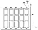
도 3은 도 1의 표시패널에 형성된 제1 전원전압 라인, 제2 전원전압 라인, 및 캐소드 전극을 상세히 보여주는 평면도.
도 4는 본 발명의 실시 예에 따른 표시 모드에서 유기전계발광 표시장치의 동작을 보여주는 흐름도.
도 5는 본 발명의 실시 예에 따른 에이징 모드에서 유기전계발광 표시장치의 동작을 보여주는 흐름도.
도 6은 모기판에 형성된 유기전계발광 표시패널셀과 제4 전원전압 라인을 보여주는 일 예시도면.
도 7은 모기판에 형성된 유기전계발광 표시패널셀과 제4 전원전압 라인을 보여주는 또 다른 예시도면.1 is a block diagram illustrating an organic light emitting display device according to an exemplary embodiment of the present invention.
2 is an equivalent circuit diagram illustrating an example of a pixel of FIG. 1.
3 is a plan view illustrating in detail a first power voltage line, a second power voltage line, and a cathode electrode formed on the display panel of FIG. 1;
4 is a flowchart illustrating an operation of an organic light emitting display device in a display mode according to an exemplary embodiment of the present invention.
5 is a flowchart illustrating an operation of an organic light emitting display device in an aging mode according to an exemplary embodiment of the present invention.
6 is an exemplary diagram illustrating an organic light emitting display panel cell and a fourth power voltage line formed on a mother substrate.
FIG. 7 is another exemplary view illustrating an organic light emitting display panel cell and a fourth power voltage line formed on a mother substrate. FIG.
이하 첨부된 도면을 참조하여 유기전계발광 표시장치를 중심으로 본 발명에 따른 바람직한 실시 예들을 상세히 설명한다. 명세서 전체에 걸쳐서 동일한 참조번호들은 실질적으로 동일한 구성요소들을 의미한다. 이하의 설명에서, 본 발명과 관련된 공지 기능 혹은 구성에 대한 구체적인 설명이 본 발명의 요지를 불필요하게 흐릴 수 있다고 판단되는 경우, 그 상세한 설명을 생략한다. 이하의 설명에서 사용되는 구성요소들의 명칭은 명세서 작성의 용이함을 고려하여 선택된 것으로, 실제 제품의 명칭과는 상이할 수 있다.
Hereinafter, exemplary embodiments of the present invention will be described in detail with reference to the accompanying drawings. Like numbers refer to like elements throughout. In the following description, when it is determined that a detailed description of known functions or configurations related to the present invention may unnecessarily obscure the subject matter of the present invention, the detailed description thereof will be omitted. The names of the components used in the following description are selected in consideration of the ease of preparation of the specification, and may be different from the names of the actual products.
도 1은 본 발명의 실시 예에 따른 유기전계발광 표시장치를 보여주는 블록도이다. 도 1을 참조하면, 본 발명의 실시 예에 따른 유기전계발광 표시장치는 표시패널(10), 데이터 구동부(20), 스캔 구동부(30), 타이밍 제어부(40), 전원부(50) 등을 구비한다.1 is a block diagram illustrating an organic light emitting display device according to an exemplary embodiment of the present invention. Referring to FIG. 1, an organic light emitting display device according to an exemplary embodiment includes a
표시패널(10)에는 데이터 라인들(DL1~DLm, m은 2 이상의 자연수)과 스캔 라인들(SL1~SLn, n은 2 이상의 자연수)이 서로 교차되도록 형성된다. 또한, 표시패널(10)에는 스캔 라인들(SL1~SLn)과 나란하게 초기화 라인들(IL1~ILn), 및 발광 라인들(EML1~EMLn)이 형성된다. 또한, 표시패널(10)에는 매트릭스 형태로 배치된 화소(P)들이 형성된다. 표시패널(10)의 화소(P)에 대한 자세한 설명은 도 3을 결부하여 후술한다.The
데이터 구동부(20)는 적어도 하나의 소스 드라이브 IC를 포함한다. 소스 드라이브 IC는 타이밍 제어부(40)로부터 디지털 비디오 데이터(DATA)를 입력받는다. 소스 드라이브 IC들은 타이밍 제어부(40)로부터의 소스 타이밍 제어신호(DCS)에 응답하여 디지털 비디오 데이터(DATA)를 감마보상전압으로 변환하여 데이터 전압들을 발생하고, 데이터 전압들을 스캔 신호에 동기되도록 표시패널(10)의 데이터 라인(DL)들에 공급한다. 이에 따라, 스캔 신호(SCAN)가 공급되는 화소(P)들 각각에 데이터 전압이 공급된다.The
스캔 구동부(30)는 스캔 신호 구동회로, 초기화 신호 구동회로, 발광 신호 구동회로 등을 포함한다. 스캔 신호 구동회로, 초기화 신호 구동회로 및 발광 신호 구동회로 각각은 순차적으로 출력신호를 발생하는 쉬프트 레지스터, 쉬프트 레지스터의 출력신호를 화소(P)의 트랜지스터 구동에 적합한 스윙폭으로 변환하기 위한 레벨 쉬프터, 및 출력 버퍼 등을 포함할 수 있다.The
스캔 신호 구동회로는 표시패널(10)의 스캔 라인들(SL1~SLn)에 스캔 신호를 순차적으로 공급한다. 초기화 신호 구동회로는 표시패널(10)의 초기화 라인들(IL1~ILn)에 초기화 신호를 순차적으로 공급한다. 발광 신호 구동회로는 표시패널(10)의 발광 라인들(EML1~EMLn)에 발광 신호를 순차적으로 공급한다.The scan signal driver circuit sequentially supplies the scan signals to the scan lines SL1 to SLn of the
타이밍 제어부(40)는 LVDS(Low Voltage Differential Signaling) 인터페이스, TMDS(Transition Minimized Differential Signaling) 인터페이스 등의 인터페이스를 통해 호스트 시스템(미도시)으로부터 디지털 비디오 데이터(DATA)를 입력받는다. 또한, 타이밍 제어부(40)는 호스트 시스템(미도시)으로부터 수직 동기신호, 수평 동기신호, 데이터 인에이블 신호(Data Enable), 도트 클럭(Dot Clock) 등의 타이밍 신호를 입력받는다.The
타이밍 제어부(40)는 타이밍 신호에 기초하여 데이터 구동부(20)와 스캔 구동부(30)의 동작 타이밍을 제어하기 위한 타이밍 제어신호들을 발생한다. 타이밍 제어신호들은 스캔 구동부(30)의 동작 타이밍을 제어하기 위한 스캔 타이밍 제어신호(SCS), 데이터 구동부(20)의 동작 타이밍을 제어하기 위한 데이터 타이밍 제어신호(DCS)를 포함한다. 타이밍 제어부(40)는 스캔 타이밍 제어신호(SCS)를 스캔 구동부(30)로 출력하고, 데이터 타이밍 제어신호(DCS)와 디지털 비디오 데이터(DATA)를 데이터 구동부(20)로 출력한다.The
전원부(50)는 유기전계발광 표시장치에 내장된 배터리 또는 외부의 전원공급원으로부터 소정의 전압을 공급받고, 제1 내지 제3 전원전압 라인(VSL1, VSL2, VSL3) 각각에 소정의 전원전압을 공급한다. 제1 전원전압 라인(VSL1)은 화소(P)들 각각의 유기발광다이오드 소자의 캐소드 전극(CAT)과 접속된다. 제2 및 제3 전원전압 라인(VSL2, VSL3) 각각은 화소(P)들 각각에 접속된다.
The
또한, 전원부(50)는 스캔 구동부(30)에 게이트 하이 전압과 게이트 로우 전압을 공급할 수 있다. 제1 내지 제3 전원전압 라인들(VSL1, VSL2, VSL3) 및 캐소드 전극(CAT)에 대한 자세한 설명은 도 3을 결부하여 후술한다.
In addition, the
도 2는 도 1의 화소의 일 예를 보여주는 등가 회로도이다. 도 2를 참조하면, 본 발명의 실시 예에 따른 화소(P)는 구동 트랜지스터(transistor)(DT), 유기발광다이오드 소자(Organic Light Emitting Diode, OLED), 다수의 스위치 트랜지스터(ST1, ST2, ST3, ST4, ST5), 및 캐패시터(capacitor) 등을 포함한다. 본 발명의 실시 예에 따른 화소(P)는 구동 트랜지스터(DT)의 문턱전압(Vth)을 보상하기 위해, 스캔 라인(SL), 초기화 라인(IL) 및 발광 라인(EM)을 통해 공급되는 스캔 신호, 초기화 신호 및 발광 신호에 의해 제어되는 다수의 스위치 트랜지스터를 포함하고, 제1 내지 제3 전원전압 라인(VSL1, VSL2, VSL3)에 접속되는 것에 주의하여야 한다.2 is an equivalent circuit diagram illustrating an example of a pixel of FIG. 1. 2, a pixel P according to an exemplary embodiment of the present invention may include a driving transistor DT, an organic light emitting diode OLED, and a plurality of switch transistors ST1, ST2, and ST3. , ST4, ST5), and capacitors, and the like. The pixel P according to the exemplary embodiment of the present invention is scanned through the scan line SL, the initialization line IL, and the emission line EM to compensate for the threshold voltage Vth of the driving transistor DT. Note that a plurality of switch transistors controlled by a signal, an initialization signal, and a light emission signal are connected to the first to third power supply voltage lines VSL1, VSL2, and VSL3.
구동 트랜지스터(DT)는 게이트 전극의 전압에 따라 드레인-소스간 전류(Ids)를 제어한다. 구동 트랜지스터(DT)의 게이트-소스 간의 전압과 문턱전압 간의 차이가 클수록 구동 트랜지스터(DT)의 채널을 통해 흐르는 드레인-소스간 전류(Ids)는 커진다. 구동 트랜지스터(DT)의 게이트 전극은 제1 노드(N1)에 접속되고, 제1 전극은 제2 노드(N2)에 접속되며, 제2 전극은 제3 노드(N3)에 접속된다.The driving transistor DT controls the drain-source current Ids according to the voltage of the gate electrode. As the difference between the gate-source voltage and the threshold voltage of the driving transistor DT increases, the drain-source current Ids flowing through the channel of the driving transistor DT increases. The gate electrode of the driving transistor DT is connected to the first node N1, the first electrode is connected to the second node N2, and the second electrode is connected to the third node N3.
유기발광다이오드 소자(OLED)의 애노드 전극은 제5 트랜지스터(ST5)의 제2 전극에 접속되고, 캐소드 전극은 제1 전원전압 라인(VSL1)에 접속된다. 유기발광다이오드 소자(OLED)는 구동 트랜지스터(DT)의 드레인-소스간 전류(Ids)에 따라 발광된다. 유기발광다이오드 소자(OLED)의 발광량은 구동 트랜지스터(DT)의 드레인-소스간 전류(Ids)에 비례할 수 있다.The anode electrode of the organic light emitting diode OLED is connected to the second electrode of the fifth transistor ST5, and the cathode electrode is connected to the first power supply voltage line VSL1. The organic light emitting diode OLED emits light according to the drain-source current Ids of the driving transistor DT. The amount of light emitted by the organic light emitting diode OLED may be proportional to the drain-source current Ids of the driving transistor DT.
제1 트랜지스터(ST1)는 스캔 라인(SL)으로부터 공급되는 스캔 신호에 의해 턴-온되어 제2 노드(N2)를 데이터 라인(DL)에 접속시킨다. 이로 인해, 제2 노드(N2)에는 데이터 라인(DL)의 데이터 전압이 공급된다. 제1 트랜지스터(ST1)의 게이트 전극은 스캔 라인(SL)에 접속되고, 제1 전극은 데이터 라인(DL)에 접속되며, 제2 전극은 제2 노드(N2)에 접속된다.The first transistor ST1 is turned on by the scan signal supplied from the scan line SL to connect the second node N2 to the data line DL. Therefore, the data voltage of the data line DL is supplied to the second node N2. The gate electrode of the first transistor ST1 is connected to the scan line SL, the first electrode is connected to the data line DL, and the second electrode is connected to the second node N2.
제2 트랜지스터(ST2)는 초기화 라인(IL)으로부터 공급되는 초기화 신호에 의해 턴-온되어 제1 노드(N1)를 제3 전원전압 라인(VSL3)에 접속시킨다. 이로 인해, 제1 노드(N1)는 제3 전원전압 라인(VSL3)을 통해 공급되는 전압으로 초기화된다. 제2 트랜지스터(ST2)의 게이트 전극은 초기화 라인(IL)에 접속되고, 제1 전극은 제1 노드(N1)에 접속되며, 제2 전극은 제3 전원전압 라인(VSL3)에 접속된다.The second transistor ST2 is turned on by the initialization signal supplied from the initialization line IL to connect the first node N1 to the third power voltage line VSL3. Thus, the first node N1 is initialized to the voltage supplied through the third power supply voltage line VSL3. The gate electrode of the second transistor ST2 is connected to the initialization line IL, the first electrode is connected to the first node N1, and the second electrode is connected to the third power voltage line VSL3.
제3 트랜지스터(ST3)는 스캔 라인(SL)으로부터 공급되는 스캔 신호에 의해 턴-온되어 제1 노드(N1)를 제3 노드(N3)에 접속시킨다. 이 경우, 구동 트랜지스터(DT)의 게이트 전극과 제2 전극이 접속되므로, 구동 트랜지스터(DT)는 다이오드(diode)로 구동된다. 제3 트랜지스터(ST3)의 게이트 전극은 스캔 라인(SL)에 접속되고, 제1 전극은 제3 노드(N3)에 접속되며, 제2 전극은 제1 노드(N1)에 접속된다.The third transistor ST3 is turned on by the scan signal supplied from the scan line SL to connect the first node N1 to the third node N3. In this case, since the gate electrode and the second electrode of the driving transistor DT are connected, the driving transistor DT is driven by a diode. The gate electrode of the third transistor ST3 is connected to the scan line SL, the first electrode is connected to the third node N3, and the second electrode is connected to the first node N1.
제4 트랜지스터(ST4)는 발광 라인(EML)으로부터 공급되는 발광 신호에 응답하여 제2 노드(N2)를 제2 전원전압 라인(VSL2)에 접속시킨다. 이로 인해, 제2 노드(N2)에는 제2 전원전압 라인(VSL2)으로부터 공급되는 전압이 공급된다. 제4 트랜지스터(ST4)의 게이트 전극은 발광 라인(EML)에 접속되고, 제1 전극은 제2 전원전압 라인(VSL2)에 접속되며, 제2 전극은 제2 노드(N2)에 접속된다.The fourth transistor ST4 connects the second node N2 to the second power voltage line VSL2 in response to a light emission signal supplied from the light emission line EML. Therefore, the voltage supplied from the second power supply voltage line VSL2 is supplied to the second node N2. The gate electrode of the fourth transistor ST4 is connected to the emission line EML, the first electrode is connected to the second power supply voltage line VSL2, and the second electrode is connected to the second node N2.
제5 트랜지스터(ST5)는 발광 라인(EML)으로부터 공급되는 발광 신호에 의해 턴-온되어 제3 노드(N3)를 유기발광다이오드 소자(OLED)의 애노드 전극에 접속시킨다. 제5 트랜지스터(ST5)의 게이트 전극은 발광 라인(EML)에 접속되고, 제1 전극은 제3 노드(N3)에 접속되며, 제2 전극은 유기발광다이오드 소자(OLED)의 애노드 전극에 접속된다. 제4 및 제5 트랜지스터(T4, T5)의 턴-온에 의해, 구동 트랜지스터(DT)의 드레인-소스간 전류(Ids)가 유기발광다이오드 소자(OLED)에 공급된다.The fifth transistor ST5 is turned on by the light emission signal supplied from the light emission line EML to connect the third node N3 to the anode electrode of the organic light emitting diode OLED. The gate electrode of the fifth transistor ST5 is connected to the emission line EML, the first electrode is connected to the third node N3, and the second electrode is connected to the anode electrode of the organic light emitting diode device OLED. . By the turn-on of the fourth and fifth transistors T4 and T5, the drain-source current Ids of the driving transistor DT is supplied to the organic light emitting diode OLED.
캐패시터(C)는 제1 노드(N1)와 제1 전원전압 라인(ELVDDL) 사이에 접속되어 제1 노드(N1)의 전압을 유지한다. 캐패시터(C)의 일측 전극은 제1 노드(N1)에 접속되고, 타측 전극은 제2 전원전압 라인(VSL2)에 접속된다.The capacitor C is connected between the first node N1 and the first power supply voltage line ELVDDL to maintain the voltage of the first node N1. One electrode of the capacitor C is connected to the first node N1, and the other electrode is connected to the second power supply voltage line VSL2.
제1 내지 제5 트랜지스터(ST1, ST2, ST3, ST4, ST5), 및 구동 트랜지스터(DT) 각각의 반도체 층은 a-Si, 산화물(oxide), 또는 폴리 실리콘(Poly Silicon)으로 형성될 수 있다. 또한, 본 발명의 실시 예에서 제1 내지 제5 트랜지스터(ST1, ST2, ST3, ST4, ST5), 및 구동 트랜지스터(DT)가 P 타입 MOSFET(Metal Oxide Semiconductor Field Effect Transistor)으로 형성된 것을 중심으로 설명하였으나, 이에 한정되지 않으며, N 타입 MOSFET으로 형성될 수도 있다.The semiconductor layers of each of the first to fifth transistors ST1, ST2, ST3, ST4, ST5, and the driving transistor DT may be formed of a-Si, oxide, or polysilicon. . In addition, the first to fifth transistors ST1, ST2, ST3, ST4, ST5, and the driving transistor DT in the exemplary embodiment of the present disclosure will be described with reference to a P-type MOSFET (Metal Oxide Semiconductor Field Effect Transistor). However, the present invention is not limited thereto and may be formed of an N-type MOSFET.
본 발명의 실시 예에 따른 화소(P)는 1 프레임 기간 동안 초기화 기간, 데이터 전압 공급 기간 및 발광 기간으로 구분되어 동작한다. 초기화 기간은 구동 트랜지스터(DT)의 게이트 전극에 접속된 제1 노드(N1)를 초기화시키는 기간이고, 데이터 전압 공급 기간은 구동 트랜지스터(DT)에 데이터 전압을 공급하는 기간이며, 발광 기간은 유기발광다이오드 소자(OLED)가 발광하는 기간이다.The pixel P according to an exemplary embodiment of the present invention operates by being divided into an initialization period, a data voltage supply period, and an emission period during one frame period. The initialization period is a period for initializing the first node N1 connected to the gate electrode of the driving transistor DT, the data voltage supply period is a period for supplying a data voltage to the driving transistor DT, and the emission period is an organic light emission period. It is a period during which the diode element OLED emits light.
구체적으로, 초기화 기간 동안 제1, 제2, 제4 및 제5 트랜지스터(ST1, ST2, ST4, ST5)는 턴-오프되고, 제3 트랜지스터(ST3)의 턴-온된다. 제2 트랜지스터(ST2)의 턴-온으로 인해, 제1 노드(N1)는 초기화 전압으로 초기화된다. 데이터 전압 공급 기간 동안 제2, 제4 및 제5 트랜지스터(ST2, ST4, ST5)는 턴-오프되고, 제1 및 제3 트랜지스터(ST1, ST3)는 턴-온된다. 제1 및 제3 트랜지스터(ST1, ST3)로 인해, 제1 노드(N1)와 제3 노드(N3)의 전압은 데이터 전압(Vdata)과 구동 트랜지스터(DT)의 문턱전압(Vth) 간의 차전압(Vdata-Vth)까지 상승한다. 발광 기간 동안 제1 내지 제3 트랜지스터(ST1, ST2, ST3)는 턴-오프되고, 제4 및 제5 트랜지스터(ST4, ST5)는 턴-온된다. 제4 및 제5 트랜지스터(ST4, ST5)의 턴-온으로 인해, 구동 트랜지스터(DT)는 제1 노드(N1)의 전압에 따라 드레인-소스간 전류(Ids)를 유기발광다이오드 소자(OLED)에 공급한다. 따라서, 화소(P)의 유기발광다이오드 소자(OLED)는 구동 트랜지스터(DT)의 드레인-소스간 전류(Ids)에 따라 발광하게 된다. 또한, 제1 노드(N1)의 전압은 구동 트랜지스터(DT)의 문턱전압을 포함하고 있으므로, 구동 트랜지스터(DT)의 드레인-소스간 전류(Ids)는 문턱전압에 의존하지 않는다.
Specifically, the first, second, fourth and fifth transistors ST1, ST2, ST4, ST5 are turned off and the third transistor ST3 is turned on during the initialization period. Due to the turn-on of the second transistor ST2, the first node N1 is initialized to an initialization voltage. The second, fourth and fifth transistors ST2, ST4 and ST5 are turned off and the first and third transistors ST1 and ST3 are turned on during the data voltage supply period. Due to the first and third transistors ST1 and ST3, the voltages of the first node N1 and the third node N3 are different from each other between the data voltage Vdata and the threshold voltage Vth of the driving transistor DT. Raises to (Vdata-Vth). The first to third transistors ST1, ST2, and ST3 are turned off during the light emission period, and the fourth and fifth transistors ST4 and ST5 are turned on. Due to the turn-on of the fourth and fifth transistors ST4 and ST5, the driving transistor DT generates the drain-source current Ids according to the voltage of the first node N1. To feed. Therefore, the organic light emitting diode OLED of the pixel P emits light according to the drain-source current Ids of the driving transistor DT. In addition, since the voltage of the first node N1 includes the threshold voltage of the driving transistor DT, the drain-source current Ids of the driving transistor DT does not depend on the threshold voltage.
도 3은 도 1의 표시패널에 형성된 제1 전원전압 라인, 제2 전원전압 라인, 및 캐소드 전극을 상세히 보여주는 평면도이다. 도 3에서는 설명의 편의를 위해 제1 전원전압 라인(VSL1), 제2 전원전압 라인(VSL2), 및 캐소드 전극(CAT)만을 도시하였음에 주의하여야 한다.3 is a plan view illustrating in detail a first power voltage line, a second power voltage line, and a cathode electrode formed on the display panel of FIG. 1. 3, only the first power supply voltage line VSL1, the second power supply voltage line VSL2, and the cathode electrode CAT are illustrated for convenience of description.
도 3을 참조하면, 표시패널(10)에는 화소(P)들이 형성되는 화소 어레이(pixel array, PA)가 형성되며, 화소 어레이(PA)의 하부 측면에는 데이터 구동부(20)가 실장되고, 양 측면에는 스캔 구동부(30)가 실장 또는 형성될 수 있다. 스캔 구동부(30)는 설명의 편의를 위해 생략하였음에 주의하여야 한다.Referring to FIG. 3, a pixel array PA including pixels P is formed on the
제1 전원전압 라인(VSL1)은 도 3과 같이 화소 어레이(PA)의 양 측면과 상부 측면을 둘러싸도록 형성된다. 제2 전원전압 라인(VSL2)은 화소 어레이(PA)에 형성된 화소(P)들 각각에 접속되도록 화소 어레이(PA)의 하부 측면으로부터 상부 측면까지 수직 방향(y축 방향)으로 형성된다. 또한, 제2 전원전압 라인(VSL2)은 수평 방향(x축 방향)으로 인접한 화소들의 사이마다 형성된다. 제1 및 제2 전원전압 라인(VSL1, VSL2)은 표시패널(10)의 하부 측면에서 플렉서블 인쇄회로(flexible printed circuit board) 또는 연성필름(flexible flim)에 접속되고, 플렉서블 인쇄회로 또는 연성필름는 전원부(50)가 실장된 인쇄회로보드(printed circuit board)에 접속될 수 있다.The first power supply voltage line VSL1 is formed to surround both side surfaces and the upper side surface of the pixel array PA as illustrated in FIG. 3. The second power supply voltage line VSL2 is formed in the vertical direction (y-axis direction) from the lower side to the upper side of the pixel array PA so as to be connected to each of the pixels P formed in the pixel array PA. In addition, the second power supply voltage line VSL2 is formed between the adjacent pixels in the horizontal direction (x-axis direction). The first and second power supply voltage lines VSL1 and VSL2 are connected to a flexible printed circuit board or a flexible film on the lower side of the
제3 전원전압 라인(VSL3)은 설명의 편의를 위해 생략하였음에 주의하여야 한다. 제3 전원전압 라인(VSL3)은 제2 전원전압 라인(VSL2)과 같이 형성될 수 있다. 즉, 제3 전원전압 라인(VSL3)은 화소 어레이(PA)에 형성된 화소(P)들 각각에 접속되도록 화소 어레이(PA)의 하부 측면으로부터 상부 측면까지 수직 방향(y축 방향)으로 형성되고, 또한 수평 방향(x축 방향)으로 인접한 화소들의 사이마다 형성될 수 있다. 이때, 제2 전원전압 라인(VSL2)과 제3 전원전압 라인(VSL3)은 서로 합선되지 않도록 형성되어야 하므로, 제2 전원전압 라인(VSL2)과 중첩되는 제3 전원전압 라인(VSL3)은 제2 전원전압 라인(VSL)과 서로 다른 층에 형성될 수 있다.It should be noted that the third power voltage line VSL3 is omitted for convenience of description. The third power supply voltage line VSL3 may be formed like the second power supply voltage line VSL2. That is, the third power voltage line VSL3 is formed in the vertical direction (y-axis direction) from the lower side to the upper side of the pixel array PA so as to be connected to each of the pixels P formed in the pixel array PA. It may also be formed between pixels adjacent in the horizontal direction (x-axis direction). In this case, since the second power supply voltage line VSL2 and the third power supply voltage line VSL3 should be formed so as not to be short-circuited with each other, the third power supply voltage line VSL3 overlapping the second power supply voltage line VSL2 has a second shape. The power supply line VSL may be formed on a different layer from the power voltage line VSL.
캐소드 전극(CAT)은 도 3과 같이 화소 어레이(PA) 상에 형성된다. 캐소드 전극(CAT)은 도 3과 같이 화소 어레이(PA)보다 넓은 면적을 갖는 하나의 전극으로 형성될 수 있다. 캐소드 전극(CAT)은 제1 전원전압 라인(VSL1)과 접촉되도록 형성된다.
The cathode electrode CAT is formed on the pixel array PA as shown in FIG. 3. The cathode electrode CAT may be formed as one electrode having a larger area than the pixel array PA as shown in FIG. 3. The cathode electrode CAT is formed to contact the first power voltage line VSL1.
본 발명의 실시 예에 따른 유기전계발광 표시장치는 표시 모드(display mode)와 에이징 모드(aging mode)로 구분되어 동작한다. 표시 모드는 표시패널(10)의 유기발광다이오드 소자를 발광하여 화상을 표시하는 모드를 의미하고, 에이징 모드는 유기발광다이오드 소자를 에이징하기 위해 유기발광다이오드 소자를 비발광하여 화상을 표시하지 않는 모드를 의미한다. 에이징 모드는 표시패널(10)의 제조를 완료한 후, 모듈 공정, 검사 공정 등 제품 출하 전에 수행될 수 있다. 이하에서는 도 4 및 도 5를 결부하여 표시 모드와 에이징 모드에서 유기전계발광 표시장치의 동작을 상세히 설명한다.The organic light emitting display device according to the embodiment of the present invention operates by being divided into a display mode and an aging mode. The display mode refers to a mode in which an organic light emitting diode device of the
도 4는 본 발명의 실시 예에 따른 표시 모드에서 유기전계발광 표시장치의 동작을 보여주는 흐름도이다. 도 4를 참조하여 표시 모드에서 유기전계발광 표시장치의 데이터 구동부(20), 스캔 구동부(30), 타이밍 제어부(40) 및 전원부(50)의 동작을 상세히 살펴본다.4 is a flowchart illustrating an operation of an organic light emitting display device in a display mode according to an exemplary embodiment of the present invention. An operation of the
첫 번째로, 전원부(50)는 표시 모드에서 제1 전원전압 라인(VSL1)에 제1 전원전압을 공급하고, 제2 전원전압 라인(VSL2)에 제2 전원전압을 공급하며, 제3 전원전압 라인(VSL3)에 구동 트랜지스터(DT)의 게이트 전극을 초기화하기 위한 제3 전원전압을 공급한다. 이하에서는, 설명의 편의를 위해 제1 전원전압은 저전위 전압에 해당하고, 제2 전원전압은 고전위 전압에 해당하며, 제3 전원전압은 초기화 전압에 해당하는 것을 중심으로 설명한다. 고전위 전압이 가장 높은 전압이고, 초기화 전압이 두 번째로 높은 전압이며, 저전위 전압이 가장 낮은 전압일 수 있다. (S101)First, the
두 번째로, 타이밍 제어부(40)는 표시 모드에서 호스트 시스템(미도시)으로부터 디지털 비디오 데이터(DATA)와 타이밍 신호를 입력받는다. 타이밍 제어부(40)는 타이밍 신호에 기초하여 데이터 구동부(20)의 동작 타이밍을 제어하기 위한 데이터 타이밍 제어신호(DCS)와 스캔 구동부(30)의 동작 타이밍을 제어하기 위한 스캔 타이밍 제어신호(SCS)를 발생한다. 타이밍 제어부(40)는 스캔 타이밍 제어신호(SCS)를 스캔 구동부(30)로 출력하고, 데이터 타이밍 제어신호(DCS)와 디지털 비디오 데이터(DATA)를 데이터 구동부(20)로 출력한다.Secondly, the
이로 인해, 스캔 구동부(30)는 스캔 라인들(SL1~SLn)에 스캔 신호를 순차적으로 출력하고, 초기화 라인들(IL1~ILn)에 초기화 신호를 순차적으로 출력하며, 발광 라인들(EM1~EMn)에 발광 신호를 순차적으로 출력한다. 또한, 데이터 구동부(20)는 디지털 비디오 데이터(DATA)로부터 변환된 데이터 전압들을 데이터 라인들(DL1~DLm)에 출력한다. (S102)Thus, the
결국, 표시 모드에서 표시패널(10)의 화소(P)들 각각은 제1 내지 제3 전원전압 라인(VSL1, VSL2, VSL3)으로부터 고전위 전압, 초기화 전압 및 저전위 전압을 공급받고, 스캔 라인(SL)으로부터 스캔 신호, 초기화 라인(IL)으로부터 초기화 신호, 발광 라인(EML)으로부터 발광 신호를 입력받으므로, 도 2를 결부하여 설명한 바와 같이 구동 트랜지스터(DT)의 드레인-소스간 전류를 유기발광다이오드 소자(OLED)에 공급할 수 있다. 따라서, 화소(P)들 각각의 유기발광다이오드 소자(OLED)는 발광하므로, 표시패널(10)은 화상을 표시하게 된다.
As a result, each of the pixels P of the
도 5는 본 발명의 실시 예에 따른 에이징 모드에서 유기전계발광 표시장치의 동작을 보여주는 흐름도이다. 도 5를 참조하여 에이징 모드에서 유기전계발광 표시장치의 데이터 구동부(20), 스캔 구동부(30), 타이밍 제어부(40) 및 전원부(50)의 동작을 상세히 살펴본다.5 is a flowchart illustrating an operation of an organic light emitting display device in an aging mode according to an exemplary embodiment of the present invention. Referring to FIG. 5, operations of the
첫 번째로, 전원부(50)는 에이징 모드에서 제1 내지 제3 전원전압 라인(VSL1~VSL3) 각각에 고전위 전압을 공급한다. 고전위 전압은 표시 모드에서 제2 전원전압 라인(VSL2)에 공급되는 전압이다. 한편, 제1 내지 제3 전원전압 라인(VSL1~VSL3)에 공급되는 전압은 고전위 전압으로 한정되지 않음에 주의하여야 한다. 제1 내지 제3 전원전압 라인(VSL1~VSL3)에 공급되는 전압은 고전위 전압보다 높은 레벨 전압일 수 있다. (S201)First, the
두 번째로, 타이밍 제어부(40)는 에이징 모드에서 호스트 시스템(미도시)으로부터 디지털 비디오 데이터(DATA)와 타이밍 신호를 입력받지 않는다. 따라서, 타이밍 제어부(40)는 데이터 타이밍 제어신호(DCS)와 스캔 타이밍 제어신호(SCS)를 발생하지 않으므로, 스캔 타이밍 제어신호(SCS)를 스캔 구동부(30)로 출력하고, 데이터 타이밍 제어신호(DCS)와 디지털 비디오 데이터(DATA)를 데이터 구동부(20)로 출력하지 않는다.Secondly, the
이로 인해, 스캔 구동부(30)는 스캔 라인들(SL1~SLn)에 스캔 신호를 출력하지 않고, 초기화 라인들(IL1~ILn)에 초기화 신호를 출력하지 않으며, 발광 라인들(EM1~EMn)에 발광 신호를 출력하지 않는다. 또한, 데이터 구동부(20)는 데이터 전압들을 데이터 라인들(DL1~DLm)에 출력하지 않는다. (S102)Accordingly, the
결국, 에이징 모드에서 표시패널(10)의 화소(P)들 각각은 제1 내지 제3 전원전압 라인(VSL1, VSL2, VSL3)으로부터 고전위 전압을 공급받으며, 스캔 라인(SL)으로부터 스캔 신호, 초기화 라인(IL)으로부터 초기화 신호, 발광 라인(EML)으로부터 발광 신호를 공급받지 않는다. 이로 인해, 화소(P)들 각각의 스위치 트랜지스터들은 턴-오프되므로, 화소(P)들 각각의 유기발광다이오드 소자(OLED)는 발광하지 않는다. 특히, 화소(P)들 각각의 유기발광다이오드 소자(OLED)가 발광하지 않기 위해서는, 유기발광다이오드 소자(OLED)에 전류가 흐르지 않아야 하므로, 유기발광다이오드 소자(OLED)의 캐소드 전극에 공급되는 전압이 유기발광다이오드 소자(OLED)의 애노드 전극의 전압보다 높아야 한다.As a result, in the aging mode, each of the pixels P of the
한편, 제1 내지 제3 전원전압 라인(VSL1, VSL2, VSL3)에는 고전위 전압이 공급하는 경우, 제1 내지 제3 전원전압 라인(VSL1, VSL2, VSL3) 각각에는 높은 전압으로 인해 줄열이 발생하게 된다. 줄열은 저항이 큰 배선에 전압이 인가되는 경우 저항에 의해 발생하는 열을 의미한다. 제1 내지 제3 전원전압 라인(VSL1, VSL2, VSL3) 각각은 표시패널(10)의 전 영역에 걸쳐 형성되며, 배선 저항은 길이에 비례하고 단면적에 반비례하므로, 제1 내지 제3 전원전압 라인(VSL1, VSL2, VSL3) 각각의 배선 저항은 크다고 할 수 있다. 결국, 본 발명의 실시 예는 에이징 모드에서 제1 내지 제3 전원전압 라인(VSL1, VSL2, VSL3)에 줄열을 이용하여 유기발광다이오드 소자(OLED)에 소정의 기간 동안 열을 가할 수 있으므로, 유기발광다이오드 소자(OLED)의 에이징이 가능하다.Meanwhile, when a high potential voltage is supplied to the first to third power voltage lines VSL1, VSL2, and VSL3, Joule heat is generated due to a high voltage to each of the first to third power voltage lines VSL1, VSL2, and VSL3. Done. Joule heat means heat generated by a resistor when a voltage is applied to a wiring having a large resistance. Each of the first to third power supply voltage lines VSL1, VSL2, and VSL3 is formed over the entire area of the
특히, 종래에 에이징을 하기 위해서는, 제조 공정 중에 유기발광다이오드 소자가 형성된 기판을 대략 48시간 동안 70℃의 고온의 챔버에 수납하였어야만 했다. 하지만, 본 발명의 실시 예는 에이징 모드를 이용하여 모듈 공정 또는 세트 공정 후에 에이징을 수행할 수 있다. 모듈 공정은 표시패널(10)에 표시패널(10)을 지지하는 가이드/케이스 부재를 조립하고, 데이터 구동부(20)를 표시패널(10) 상에 실장하며, 타이밍 제어부(40)와 전원부(50) 등이 실장된 인쇄회로보드(printed circuit board)를 표시패널(10)에 연결하는 공정이다. 세트 공정은 완성된 모듈에 케이스를 씌워 완제품으로 출하하는 공정을 의미한다. 결국, 본 발명의 실시 예는 모듈 공정 또는 세트 공정 중에 에이징 모드를 이용하여 유기발광다이오드 소자(OLED)를 에이징할 수 있으므로, 종래 에이징을 위해 고온의 챔버에 수납되는 시간을 줄이거나 생략할 수 있다.In particular, in order to aging conventionally, the substrate on which the organic light emitting diode element was formed had to be stored in a high temperature chamber at 70 ° C. for approximately 48 hours during the manufacturing process. However, embodiments of the present invention may perform aging after a module process or a set process using an aging mode. The module process assembles the guide / case member for supporting the
한편, 본 발명의 실시 예는 에이징 모드에서 제1 내지 제3 전원전압 라인(VSL1, VSL2, VSL3) 모두에 고전위 전압을 공급하는 것을 중심으로 설명하였으나, 이에 한정되지 않음에 주의하여야 한다. 즉, 본 발명의 실시 예는 에이징 모드에서 제1 내지 제3 전원전압 라인(VSL1, VSL2, VSL3) 중 어느 하나에 고전위 전압을 공급할 수도 있고, 제1 내지 제3 전원전압 라인(VSL1, VSL2, VSL3) 중 어느 두 개에 고전위 전압을 공급할 수도 있다.In the meantime, an embodiment of the present invention has been described focusing on supplying a high potential voltage to all of the first to third power supply voltage lines VSL1, VSL2, and VSL3 in an aging mode, but the present invention is not limited thereto. That is, the embodiment of the present invention may supply a high potential voltage to any one of the first to third power supply voltage lines VSL1, VSL2, and VSL3 in the aging mode, and the first to third power supply voltage lines VSL1 and VSL2. , VSL3) may be supplied with a high potential voltage.
이상에서 살펴본 바와 같이, 본 발명의 실시 예는 에이징 모드에서 화소(P)들은 동작하지 않으며, 제1 내지 제3 전원전압 라인(VSL1, VSL2, VSL3)에 고전위 전압을 공급하여 줄열을 발생시킨다. 그 결과, 본 발명의 실시 예는 모듈 공정 또는 세트 공정 중에 에이징 모드에서 줄열을 이용하여 유기발광다이오드 소자(OLED)를 에이징할 수 있으므로, 종래 고온의 챔버에 수납하여 에이징하는 시간을 줄이거나 생략할 수 있다.
As described above, in the exemplary embodiment of the present invention, the pixels P do not operate in the aging mode and generate Joule heat by supplying high potential voltages to the first to third power voltage lines VSL1, VSL2, and VSL3. . As a result, according to the embodiment of the present invention, the organic light emitting diode device (OLED) may be aged by using Joule heat in an aging mode during a module process or a set process. Can be.
앞서, 도 1 내지 도 5를 결부하여 모듈 공정 또는 세트 공정 중에 유기전계발광 표시장치의 유기발광다이오드 소자(OLED)를 에이징하는 방법에 대하여 살펴보았다. 하지만, 본 발명의 실시 예에 따른 에이징은 모기판(mother substrate)에 다수의 표시패널셀을 완성한 후 스크라이빙(scribing) 공정 전에 수행될 수도 있다. 이하에서는, 도 6 및 도 7을 결부하여 모기판(mother substrate)에 다수의 표시패널셀을 완성한 후 스크라이빙(scribing) 공정 전에 유기발광다이오드 소자(OLED)를 에이징하는 방법에 대하여 상세히 설명한다. 스크라이빙 공정은 모기판에 형성된 다수의 표시패널셀을 커팅하는 공정을 의미한다. 모기판에 형성된 다수의 표시패널셀 각각은 도 1 및 도 3에 도시된 표시패널(10)과 실질적으로 동일하다.1 to 5, a method of aging an organic light emitting diode (OLED) of an organic light emitting display device during a module process or a set process has been described. However, the aging according to the embodiment of the present invention may be performed before the scribing process after completing the plurality of display panel cells on the mother substrate. Hereinafter, a method of aging an organic light emitting diode device (OLED) before completing a scribing process after completing the plurality of display panel cells on a mother substrate in conjunction with FIGS. 6 and 7 will be described in detail. . The scribing process refers to a process of cutting a plurality of display panel cells formed on the mother substrate. Each of the plurality of display panel cells formed on the mother substrate is substantially the same as the
도 6은 모기판에 형성된 유기전계발광 표시패널셀과 제4 전원전압 라인을 보여주는 일 예시도면이다. 도 6을 참조하면, 모기판(MS)에는 다수의 표시패널셀(10)이 형성된다. 또한, 모기판(MS)에는 다수의 표시패널셀(10) 각각에 접속되는 제4 전원전압 라인(VSL4)이 형성된다. 제4 전원전압 라인(VSL4)은 모기판(MS)에 형성된 표시패널셀(10) 모두에 접속되도록 형성된다. 또한, 제4 전원전압 라인(VSL4)은 표시패널셀(10)에 형성된 제1 내지 제3 전원전압 라인(VSL1~VSL3) 모두에 접속될 수 있다. 하지만, 본 발명의 실시 예는 이에 한정되지 않으며, 제4 전원전압 라인(VSL4)은 제1 내지 제3 전원전압 라인(VSL1~VSL3) 중 어느 하나 또는 어느 두 개에 접속될 수도 있다.6 is an exemplary diagram illustrating an organic light emitting display panel cell and a fourth power voltage line formed on a mother substrate. Referring to FIG. 6, a plurality of
또한, 모기판(MS)에는 지그(jig) 등을 통해 제4 전원전압 라인(VSL4)에 소정의 전압을 공급하기 위한 전압 입력 단자(VIT)가 형성될 수 있다. 소정의 전압은 고전위 전압 또는 고전위 전압보다 높은 레벨의 전압일 수 있다. 전원 입력 단자(VIT)는 제4 전원전압 라인(VSL4)의 위치에 따라 전위 차이가 발생하지 않도록 복수 개 형성될 수 있다.In addition, a voltage input terminal VIT may be formed in the mother substrate MS for supplying a predetermined voltage to the fourth power voltage line VSL4 through a jig or the like. The predetermined voltage may be a high potential voltage or a voltage at a level higher than the high potential voltage. The power input terminal VIT may be formed in plural such that a potential difference does not occur according to the position of the fourth power voltage line VSL4.
결국, 본 발명의 실시 예는 모기판(MS)에 다수의 표시패널셀을 완성한 후 스크라이빙 공정 전에 모기판(MS)의 전원 입력 단자(VIT)에 고전위 전압을 공급함으로써, 다수의 표시패널셀(10) 각각의 제1 내지 제3 전원전압 라인(VSL1~VSL3)에 고전위 전압을 공급할 수 있다. 이로 인해, 제1 내지 제3 전원전압 라인(VSL1~VSL3)에는 줄열이 발생할 수 있다. 따라서, 본 발명의 실시 예는 모기판에 다수의 표시패널셀을 완성한 후 스크라이빙 공정 전에 줄열을 이용하여 유기발광다이오드 소자(OLED)를 에이징할 수 있으므로, 종래 고온의 챔버에 수납하여 에이징하는 시간을 줄이거나 생략할 수 있다.As a result, an embodiment of the present invention provides a plurality of displays by supplying a high potential voltage to the power input terminal VIT of the mother substrate MS after completing the plurality of display panel cells on the mother substrate MS and before the scribing process. The high potential voltage may be supplied to the first to third power supply voltage lines VSL1 to VSL3 of each
도 7은 모기판에 형성된 유기전계발광 표시패널셀과 제4 전원전압 라인을 보여주는 또 다른 예시도면이다. 도 7에 도시된 모기판에 형성된 유기전계발광 표시패널셀과 제4 전원전압 라인의 또 다른 예시도면은 제4 전원전압 라인(VSL4)이 수직 방향(y축 방향)으로 나란하게 배열된 다수의 표시패널셀(10)에 접속되는 것을 제외하고는 도 6에서 설명한 바와 실질적으로 동일하다. 본 발명의 실시 예는 제4 전원전압 라인(VSL4)이 수평 방향(x축 방향)으로 나란하게 배열된 다수의 표시패널셀(10)에 접속될 수도 있다.
FIG. 7 is another exemplary view illustrating an organic light emitting display panel cell and a fourth power voltage line formed on a mother substrate. In another exemplary embodiment of the organic light emitting display panel cell and the fourth power voltage line formed on the mother substrate shown in FIG. 7, a plurality of fourth power voltage lines VSL4 are arranged side by side in the vertical direction (y-axis direction). It is substantially the same as described in FIG. 6 except that it is connected to the
이상 설명한 내용을 통해 당업자라면 본 발명의 기술사상을 일탈하지 아니하는 범위에서 다양한 변경 및 수정이 가능함을 알 수 있을 것이다. 따라서, 본 발명의 기술적 범위는 명세서의 상세한 설명에 기재된 내용으로 한정되는 것이 아니라 특허 청구의 범위에 의해 정하여져야만 할 것이다.
Those skilled in the art will appreciate that various changes and modifications can be made without departing from the technical spirit of the present invention. Therefore, the technical scope of the present invention should not be limited to the contents described in the detailed description of the specification but should be defined by the claims.
10: 표시패널20: 데이터 구동부
30: 스캔 구동부40: 타이밍 제어부
50: 전원부VSL1: 제1 전원전압 라인
VSL2: 제2 전원전압 라인VSL3: 제3 전원전압 라인10: display panel 20: data driver
30: scan driver 40: timing controller
50: power supply unit VSL1: first power supply voltage line
VSL2: second power supply voltage line VSL3: third power supply voltage line
Claims (13)
Translated fromKorean상기 제1 전원전압 라인은 상기 유기발광다이오드 소자의 캐소드 전극에 접속되며,
상기 유기발광다이오드 소자가 발광하는 표시 모드에서 상기 제1 전원전압 라인에 공급되는 전압은 상기 유기발광다이오드 소자가 비발광하는 에이징 모드에서 상기 제1 전원전압 라인에 공급되는 전압보다 낮고,
상기 에이징 모드에서 상기 다수의 스위치 트랜지스터들은 모두 턴-오프되는 것을 특징으로 하는 유기전계발광 표시장치.A display panel including a driving transistor, a plurality of switch transistors, and pixels including an organic light emitting diode element, and a first power supply voltage line connected to each of the pixels,
The first power supply voltage line is connected to a cathode of the organic light emitting diode element,
The voltage supplied to the first power supply voltage line in the display mode in which the organic light emitting diode emits light is lower than the voltage supplied to the first power supply voltage line in the aging mode in which the organic light emitting diode device does not emit light.
And the plurality of switch transistors are all turned off in the aging mode.
상기 표시패널에는 상기 화소들 각각에 접속된 제2 전원전압 라인이 더 형성되고,
상기 에이징 모드에서 상기 제2 전원전압 라인에 공급되는 전압은 상기 표시 모드에서 상기 제1 전원전압 라인에 공급되는 전압보다 높은 것을 특징으로 하는 유기전계발광 표시장치.The method of claim 1,
The display panel further includes a second power supply voltage line connected to each of the pixels,
And the voltage supplied to the second power supply voltage line in the aging mode is higher than the voltage supplied to the first power supply voltage line in the display mode.
상기 에이징 모드에서 상기 제2 전원전압 라인에 공급되는 전압은 상기 표시 모드에서 상기 제2 전원전압 라인에 공급되는 전압과 동일한 것을 특징으로 하는 유기전계발광 표시장치.The method of claim 3, wherein
And the voltage supplied to the second power voltage line in the aging mode is the same as the voltage supplied to the second power voltage line in the display mode.
상기 에이징 모드에서 상기 제2 전원전압 라인에 공급되는 전압은 상기 에이징 모드에서 상기 제1 전원전압 라인에 공급되는 전압과 동일한 것을 특징으로 하는 유기전계발광 표시장치.The method of claim 3, wherein
And the voltage supplied to the second power supply voltage line in the aging mode is the same as the voltage supplied to the first power supply voltage line in the aging mode.
상기 표시패널에는 상기 화소들 각각에 접속된 제3 전원전압 라인이 더 형성되고,
상기 에이징 모드에서 상기 제3 전원전압 라인에 공급되는 전압은 상기 표시 모드에서 상기 제1 전원전압 라인에 공급되는 전압보다 높은 것을 특징으로 하는 유기전계발광 표시장치.The method of claim 3, wherein
The display panel further includes a third power supply voltage line connected to each of the pixels,
And the voltage supplied to the third power voltage line in the aging mode is higher than the voltage supplied to the first power voltage line in the display mode.
상기 에이징 모드에서 상기 제3 전원전압 라인에 공급되는 전압은 상기 표시 모드에서 상기 제2 전원전압 라인에 공급되는 전압과 동일한 것을 특징으로 하는 유기전계발광 표시장치.The method of claim 6,
And the voltage supplied to the third power voltage line in the aging mode is the same as the voltage supplied to the second power voltage line in the display mode.
상기 에이징 모드에서 상기 제3 전원전압 라인에 공급되는 전압은 상기 에이징 모드에서 상기 제1 전원전압 라인에 공급되는 전압과 동일한 것을 특징으로 하는 유기전계발광 표시장치.The method of claim 6,
And a voltage supplied to the third power supply voltage line in the aging mode is the same as a voltage supplied to the first power supply voltage line in the aging mode.
상기 표시 모드에서 상기 유기발광다이오드는 상기 구동 트랜지스터의 드레인-소스간 전류에 따라 발광하는 것을 특징으로 하는 유기전계발광 표시장치.The method of claim 6,
And the organic light emitting diode emits light according to the drain-source current of the driving transistor in the display mode.
상기 제1 전원전압 라인에 제1 전원전압을 공급하는 단계; 및
상기 유기발광다이오드 소자를 비발광하는 단계를 포함하고,
상기 유기발광다이오드 소자를 비발광하는 단계에서 상기 다수의 스위치 트랜지스터들은 모두 턴-오프되는 유기전계발광 표시장치의 에이징 방법.Pixels arranged in a matrix form in an area defined by the intersection structure of the data lines and the scan lines, and including a driving transistor, a plurality of switch transistors, and an organic light emitting diode element, and a first pixel connected to each of the pixels; 1. A method of aging an organic light emitting display device having a display panel having a first power supply voltage line, wherein the first power supply voltage line is connected to a cathode of the organic light emitting diode element.
Supplying a first power voltage to the first power voltage line; And
Non-emitting the organic light emitting diode device;
An aging method of an organic light emitting display device in which the plurality of switch transistors are all turned off in the step of non-emitting the organic light emitting diode device.
상기 표시패널에는 상기 화소들 각각에 접속된 제2 전원전압 라인이 더 형성되는 것을 특징으로 하고,
상기 제2 전원전압 라인에 상기 제1 전원전압을 공급하는 단계를 더 포함하는 유기전계발광 표시장치의 에이징 방법.The method of claim 10,
And a second power supply voltage line connected to each of the pixels in the display panel.
The method of claim 1, further comprising supplying the first power voltage to the second power voltage line.
상기 표시패널에는 상기 화소들 각각에 접속된 제3 전원전압 라인이 더 형성되는 것을 특징으로 하고,
상기 제3 전원전압 라인에 상기 제1 전원전압을 공급하는 단계를 더 포함하는 유기전계발광 표시장치의 에이징 방법.
The method of claim 12,
And a third power supply voltage line connected to each of the pixels in the display panel.
Aging method of the organic light emitting display device further comprising the step of supplying the first power voltage to the third power voltage line.
Priority Applications (2)
| Application Number | Priority Date | Filing Date | Title |
|---|---|---|---|
| KR1020130132751AKR102077794B1 (en) | 2013-11-04 | 2013-11-04 | Organic light emitting diode display device and method for aging the same |
| US14/530,975US9786219B2 (en) | 2013-11-04 | 2014-11-03 | Organic light emitting display and method for aging the same |
Applications Claiming Priority (1)
| Application Number | Priority Date | Filing Date | Title |
|---|---|---|---|
| KR1020130132751AKR102077794B1 (en) | 2013-11-04 | 2013-11-04 | Organic light emitting diode display device and method for aging the same |
Publications (2)
| Publication Number | Publication Date |
|---|---|
| KR20150051392A KR20150051392A (en) | 2015-05-13 |
| KR102077794B1true KR102077794B1 (en) | 2020-02-17 |
Family
ID=53006702
Family Applications (1)
| Application Number | Title | Priority Date | Filing Date |
|---|---|---|---|
| KR1020130132751AExpired - Fee RelatedKR102077794B1 (en) | 2013-11-04 | 2013-11-04 | Organic light emitting diode display device and method for aging the same |
Country Status (2)
| Country | Link |
|---|---|
| US (1) | US9786219B2 (en) |
| KR (1) | KR102077794B1 (en) |
Cited By (1)
| Publication number | Priority date | Publication date | Assignee | Title |
|---|---|---|---|---|
| US12424171B2 (en) | 2023-03-14 | 2025-09-23 | Samsung Display Co., Ltd. | Pixel and method of aging the pixel |
Families Citing this family (4)
| Publication number | Priority date | Publication date | Assignee | Title |
|---|---|---|---|---|
| CN107331338B (en)* | 2017-08-28 | 2021-08-17 | 京东方科技集团股份有限公司 | Array substrate, display device and detection method thereof |
| KR102582618B1 (en)* | 2019-02-26 | 2023-09-26 | 삼성디스플레이 주식회사 | Display device and driving method thereof |
| CN113948024B (en)* | 2021-09-28 | 2024-07-19 | 惠科股份有限公司 | Display panel aging test method and device, display panel and storage medium |
| CN114822332B (en)* | 2022-03-23 | 2025-05-16 | 重庆惠科金渝光电科技有限公司 | Display panel detection method, display device and central control circuit |
Citations (1)
| Publication number | Priority date | Publication date | Assignee | Title |
|---|---|---|---|---|
| JP2013109868A (en)* | 2011-11-18 | 2013-06-06 | Panasonic Corp | Method of manufacturing display device, and display device |
Family Cites Families (15)
| Publication number | Priority date | Publication date | Assignee | Title |
|---|---|---|---|---|
| US6646284B2 (en)* | 2000-12-12 | 2003-11-11 | Semiconductor Energy Laboratory Co., Ltd. | Light emitting device and method of manufacturing the same |
| US7592975B2 (en)* | 2004-08-27 | 2009-09-22 | Semiconductor Energy Laboratory Co., Ltd. | Display device and driving method thereof |
| KR100626019B1 (en) | 2004-10-14 | 2006-09-20 | 삼성에스디아이 주식회사 | Substrate of organic light emitting device, organic light emitting device using same and aging method thereof |
| JP2006210213A (en) | 2005-01-31 | 2006-08-10 | Sony Corp | Aging method, manufacturing method and aging device of self-luminous device |
| TWI450247B (en)* | 2006-02-10 | 2014-08-21 | Ignis Innovation Inc | Method and system for pixel circuit displays |
| JP2007317384A (en)* | 2006-05-23 | 2007-12-06 | Canon Inc | Organic EL display device, manufacturing method thereof, repair method and repair device |
| KR100835988B1 (en) | 2006-12-06 | 2008-06-09 | 한국전자통신연구원 | OLED element |
| JP4629715B2 (en) | 2006-12-06 | 2011-02-09 | 韓國電子通信研究院 | OLED element |
| KR100876250B1 (en)* | 2007-01-15 | 2008-12-26 | 삼성모바일디스플레이주식회사 | Organic electroluminescent display |
| KR100853540B1 (en)* | 2007-02-01 | 2008-08-21 | 삼성에스디아이 주식회사 | Organic light emitting display device and aging method |
| KR100941834B1 (en) | 2008-05-07 | 2010-02-11 | 삼성모바일디스플레이주식회사 | Mother substrate of organic light emitting display device and its aging method |
| KR101064403B1 (en)* | 2009-10-07 | 2011-09-14 | 삼성모바일디스플레이주식회사 | Mother board of organic light emitting display device capable of ledger inspection and ledger inspection method |
| KR20110043259A (en) | 2009-10-21 | 2011-04-27 | 엘지디스플레이 주식회사 | Organic light emitting display device |
| KR101113430B1 (en)* | 2009-12-10 | 2012-03-02 | 삼성모바일디스플레이주식회사 | Pixel and organic light emitting display device using the same |
| KR101152466B1 (en)* | 2010-06-30 | 2012-06-01 | 삼성모바일디스플레이주식회사 | Pixel and Organic Light Emitting Display Device Using the Same |
- 2013
- 2013-11-04KRKR1020130132751Apatent/KR102077794B1/ennot_activeExpired - Fee Related
- 2014
- 2014-11-03USUS14/530,975patent/US9786219B2/ennot_activeExpired - Fee Related
Patent Citations (1)
| Publication number | Priority date | Publication date | Assignee | Title |
|---|---|---|---|---|
| JP2013109868A (en)* | 2011-11-18 | 2013-06-06 | Panasonic Corp | Method of manufacturing display device, and display device |
Cited By (1)
| Publication number | Priority date | Publication date | Assignee | Title |
|---|---|---|---|---|
| US12424171B2 (en) | 2023-03-14 | 2025-09-23 | Samsung Display Co., Ltd. | Pixel and method of aging the pixel |
Also Published As
| Publication number | Publication date |
|---|---|
| US9786219B2 (en) | 2017-10-10 |
| KR20150051392A (en) | 2015-05-13 |
| US20150123962A1 (en) | 2015-05-07 |
Similar Documents
| Publication | Publication Date | Title |
|---|---|---|
| KR102735085B1 (en) | Display module and driving method theref | |
| CN103700342B (en) | OLED pixel circuit and driving method, display device | |
| KR102290483B1 (en) | Organic light emitting diode display and driving method thereof | |
| TWI644302B (en) | Organic light emitting display device | |
| KR101935955B1 (en) | Organic light emitting diode display device | |
| TWI626637B (en) | Display apparatus | |
| KR101868715B1 (en) | Drive circuit and drive method for active-matrix organic light-emitting diode panel | |
| JP5384051B2 (en) | Image display device | |
| KR101850149B1 (en) | Organic Light Emitting Diode Display Device | |
| JP6282823B2 (en) | Driving circuit, display device, and driving method | |
| CN108281115B (en) | Display device, display panel, driving method and gate driver circuit | |
| KR20130061596A (en) | Organic light-emitting display device | |
| CN106991971B (en) | Display device, gate driving circuit and driving method thereof | |
| US10140922B2 (en) | Pixel driving circuit and driving method thereof and display device | |
| KR102077794B1 (en) | Organic light emitting diode display device and method for aging the same | |
| US20110304593A1 (en) | Pixel driving circuit, pixel driving method and light emitting display device | |
| KR101901757B1 (en) | Organic light emitting diode display device and method of driving the same | |
| US9691324B2 (en) | Compensation data calculation method for compensating digital video data and organic light emitting display including look-up table generated using the same | |
| KR101958449B1 (en) | Organic light emitting diode display device and method for driving the same | |
| KR101837198B1 (en) | Organic light-emitting display device | |
| KR101834012B1 (en) | Organic Light Emitting Diode Display Device | |
| KR101929037B1 (en) | Organic light emitting diode display device | |
| KR101986657B1 (en) | Organic light emitting diode display device and method of driving the same | |
| KR101901354B1 (en) | Organic light emitting diode display device | |
| KR102766364B1 (en) | Display device, controller, and display driving method |
Legal Events
| Date | Code | Title | Description |
|---|---|---|---|
| PA0109 | Patent application | St.27 status event code:A-0-1-A10-A12-nap-PA0109 | |
| PG1501 | Laying open of application | St.27 status event code:A-1-1-Q10-Q12-nap-PG1501 | |
| R18-X000 | Changes to party contact information recorded | St.27 status event code:A-3-3-R10-R18-oth-X000 | |
| A201 | Request for examination | ||
| PA0201 | Request for examination | St.27 status event code:A-1-2-D10-D11-exm-PA0201 | |
| R18-X000 | Changes to party contact information recorded | St.27 status event code:A-3-3-R10-R18-oth-X000 | |
| R17-X000 | Change to representative recorded | St.27 status event code:A-3-3-R10-R17-oth-X000 | |
| E902 | Notification of reason for refusal | ||
| PE0902 | Notice of grounds for rejection | St.27 status event code:A-1-2-D10-D21-exm-PE0902 | |
| E13-X000 | Pre-grant limitation requested | St.27 status event code:A-2-3-E10-E13-lim-X000 | |
| P11-X000 | Amendment of application requested | St.27 status event code:A-2-2-P10-P11-nap-X000 | |
| P13-X000 | Application amended | St.27 status event code:A-2-2-P10-P13-nap-X000 | |
| E701 | Decision to grant or registration of patent right | ||
| PE0701 | Decision of registration | St.27 status event code:A-1-2-D10-D22-exm-PE0701 | |
| GRNT | Written decision to grant | ||
| PR0701 | Registration of establishment | St.27 status event code:A-2-4-F10-F11-exm-PR0701 | |
| PR1002 | Payment of registration fee | St.27 status event code:A-2-2-U10-U11-oth-PR1002 Fee payment year number:1 | |
| PG1601 | Publication of registration | St.27 status event code:A-4-4-Q10-Q13-nap-PG1601 | |
| P22-X000 | Classification modified | St.27 status event code:A-4-4-P10-P22-nap-X000 | |
| PC1903 | Unpaid annual fee | St.27 status event code:A-4-4-U10-U13-oth-PC1903 Not in force date:20230211 Payment event data comment text:Termination Category : DEFAULT_OF_REGISTRATION_FEE | |
| PC1903 | Unpaid annual fee | St.27 status event code:N-4-6-H10-H13-oth-PC1903 Ip right cessation event data comment text:Termination Category : DEFAULT_OF_REGISTRATION_FEE Not in force date:20230211 | |
| P22-X000 | Classification modified | St.27 status event code:A-4-4-P10-P22-nap-X000 |