KR102077641B1 - Phase-change material layer and method of manufacturing the same - Google Patents
Phase-change material layer and method of manufacturing the sameDownload PDFInfo
- Publication number
- KR102077641B1 KR102077641B1KR1020130092857AKR20130092857AKR102077641B1KR 102077641 B1KR102077641 B1KR 102077641B1KR 1020130092857 AKR1020130092857 AKR 1020130092857AKR 20130092857 AKR20130092857 AKR 20130092857AKR 102077641 B1KR102077641 B1KR 102077641B1
- Authority
- KR
- South Korea
- Prior art keywords
- phase change
- change material
- material film
- impurity
- composition
- Prior art date
- Legal status (The legal status is an assumption and is not a legal conclusion. Google has not performed a legal analysis and makes no representation as to the accuracy of the status listed.)
- Active
Links
Images


Classifications
- H—ELECTRICITY
- H10—SEMICONDUCTOR DEVICES; ELECTRIC SOLID-STATE DEVICES NOT OTHERWISE PROVIDED FOR
- H10B—ELECTRONIC MEMORY DEVICES
- H10B63/00—Resistance change memory devices, e.g. resistive RAM [ReRAM] devices
- H10B63/20—Resistance change memory devices, e.g. resistive RAM [ReRAM] devices comprising selection components having two electrodes, e.g. diodes
- H—ELECTRICITY
- H10—SEMICONDUCTOR DEVICES; ELECTRIC SOLID-STATE DEVICES NOT OTHERWISE PROVIDED FOR
- H10N—ELECTRIC SOLID-STATE DEVICES NOT OTHERWISE PROVIDED FOR
- H10N70/00—Solid-state devices having no potential barriers, and specially adapted for rectifying, amplifying, oscillating or switching
- H10N70/20—Multistable switching devices, e.g. memristors
- H10N70/231—Multistable switching devices, e.g. memristors based on solid-state phase change, e.g. between amorphous and crystalline phases, Ovshinsky effect
- H—ELECTRICITY
- H10—SEMICONDUCTOR DEVICES; ELECTRIC SOLID-STATE DEVICES NOT OTHERWISE PROVIDED FOR
- H10N—ELECTRIC SOLID-STATE DEVICES NOT OTHERWISE PROVIDED FOR
- H10N70/00—Solid-state devices having no potential barriers, and specially adapted for rectifying, amplifying, oscillating or switching
- H10N70/801—Constructional details of multistable switching devices
- H10N70/881—Switching materials
- H10N70/882—Compounds of sulfur, selenium or tellurium, e.g. chalcogenides
- H10N70/8828—Tellurides, e.g. GeSbTe
- C—CHEMISTRY; METALLURGY
- C23—COATING METALLIC MATERIAL; COATING MATERIAL WITH METALLIC MATERIAL; CHEMICAL SURFACE TREATMENT; DIFFUSION TREATMENT OF METALLIC MATERIAL; COATING BY VACUUM EVAPORATION, BY SPUTTERING, BY ION IMPLANTATION OR BY CHEMICAL VAPOUR DEPOSITION, IN GENERAL; INHIBITING CORROSION OF METALLIC MATERIAL OR INCRUSTATION IN GENERAL
- C23C—COATING METALLIC MATERIAL; COATING MATERIAL WITH METALLIC MATERIAL; SURFACE TREATMENT OF METALLIC MATERIAL BY DIFFUSION INTO THE SURFACE, BY CHEMICAL CONVERSION OR SUBSTITUTION; COATING BY VACUUM EVAPORATION, BY SPUTTERING, BY ION IMPLANTATION OR BY CHEMICAL VAPOUR DEPOSITION, IN GENERAL
- C23C16/00—Chemical coating by decomposition of gaseous compounds, without leaving reaction products of surface material in the coating, i.e. chemical vapour deposition [CVD] processes
- C23C16/22—Chemical coating by decomposition of gaseous compounds, without leaving reaction products of surface material in the coating, i.e. chemical vapour deposition [CVD] processes characterised by the deposition of inorganic material, other than metallic material
- C23C16/30—Deposition of compounds, mixtures or solid solutions, e.g. borides, carbides, nitrides
- C23C16/305—Sulfides, selenides, or tellurides
- C—CHEMISTRY; METALLURGY
- C30—CRYSTAL GROWTH
- C30B—SINGLE-CRYSTAL GROWTH; UNIDIRECTIONAL SOLIDIFICATION OF EUTECTIC MATERIAL OR UNIDIRECTIONAL DEMIXING OF EUTECTOID MATERIAL; REFINING BY ZONE-MELTING OF MATERIAL; PRODUCTION OF A HOMOGENEOUS POLYCRYSTALLINE MATERIAL WITH DEFINED STRUCTURE; SINGLE CRYSTALS OR HOMOGENEOUS POLYCRYSTALLINE MATERIAL WITH DEFINED STRUCTURE; AFTER-TREATMENT OF SINGLE CRYSTALS OR A HOMOGENEOUS POLYCRYSTALLINE MATERIAL WITH DEFINED STRUCTURE; APPARATUS THEREFOR
- C30B29/00—Single crystals or homogeneous polycrystalline material with defined structure characterised by the material or by their shape
- C30B29/10—Inorganic compounds or compositions
- C30B29/46—Sulfur-, selenium- or tellurium-containing compounds
- H—ELECTRICITY
- H10—SEMICONDUCTOR DEVICES; ELECTRIC SOLID-STATE DEVICES NOT OTHERWISE PROVIDED FOR
- H10B—ELECTRONIC MEMORY DEVICES
- H10B63/00—Resistance change memory devices, e.g. resistive RAM [ReRAM] devices
- H10B63/80—Arrangements comprising multiple bistable or multi-stable switching components of the same type on a plane parallel to the substrate, e.g. cross-point arrays
- H—ELECTRICITY
- H10—SEMICONDUCTOR DEVICES; ELECTRIC SOLID-STATE DEVICES NOT OTHERWISE PROVIDED FOR
- H10N—ELECTRIC SOLID-STATE DEVICES NOT OTHERWISE PROVIDED FOR
- H10N70/00—Solid-state devices having no potential barriers, and specially adapted for rectifying, amplifying, oscillating or switching
- H10N70/011—Manufacture or treatment of multistable switching devices
- H10N70/021—Formation of switching materials, e.g. deposition of layers
- H10N70/023—Formation of switching materials, e.g. deposition of layers by chemical vapor deposition, e.g. MOCVD, ALD
- H—ELECTRICITY
- H10—SEMICONDUCTOR DEVICES; ELECTRIC SOLID-STATE DEVICES NOT OTHERWISE PROVIDED FOR
- H10N—ELECTRIC SOLID-STATE DEVICES NOT OTHERWISE PROVIDED FOR
- H10N70/00—Solid-state devices having no potential barriers, and specially adapted for rectifying, amplifying, oscillating or switching
- H10N70/011—Manufacture or treatment of multistable switching devices
- H10N70/061—Shaping switching materials
- H10N70/066—Shaping switching materials by filling of openings, e.g. damascene method
- H—ELECTRICITY
- H10—SEMICONDUCTOR DEVICES; ELECTRIC SOLID-STATE DEVICES NOT OTHERWISE PROVIDED FOR
- H10N—ELECTRIC SOLID-STATE DEVICES NOT OTHERWISE PROVIDED FOR
- H10N70/00—Solid-state devices having no potential barriers, and specially adapted for rectifying, amplifying, oscillating or switching
- H10N70/801—Constructional details of multistable switching devices
- H10N70/821—Device geometry
- H10N70/826—Device geometry adapted for essentially vertical current flow, e.g. sandwich or pillar type devices
- H10N70/8265—Device geometry adapted for essentially vertical current flow, e.g. sandwich or pillar type devices on sidewalls of dielectric structures, e.g. mesa-shaped or cup-shaped devices
- H—ELECTRICITY
- H10—SEMICONDUCTOR DEVICES; ELECTRIC SOLID-STATE DEVICES NOT OTHERWISE PROVIDED FOR
- H10N—ELECTRIC SOLID-STATE DEVICES NOT OTHERWISE PROVIDED FOR
- H10N70/00—Solid-state devices having no potential barriers, and specially adapted for rectifying, amplifying, oscillating or switching
- H10N70/801—Constructional details of multistable switching devices
- H10N70/821—Device geometry
- H10N70/828—Current flow limiting means within the switching material region, e.g. constrictions
- H—ELECTRICITY
- H10—SEMICONDUCTOR DEVICES; ELECTRIC SOLID-STATE DEVICES NOT OTHERWISE PROVIDED FOR
- H10N—ELECTRIC SOLID-STATE DEVICES NOT OTHERWISE PROVIDED FOR
- H10N70/00—Solid-state devices having no potential barriers, and specially adapted for rectifying, amplifying, oscillating or switching
- H10N70/801—Constructional details of multistable switching devices
- H10N70/841—Electrodes
- H10N70/8413—Electrodes adapted for resistive heating
- H—ELECTRICITY
- H10—SEMICONDUCTOR DEVICES; ELECTRIC SOLID-STATE DEVICES NOT OTHERWISE PROVIDED FOR
- H10N—ELECTRIC SOLID-STATE DEVICES NOT OTHERWISE PROVIDED FOR
- H10N70/00—Solid-state devices having no potential barriers, and specially adapted for rectifying, amplifying, oscillating or switching
- H10N70/801—Constructional details of multistable switching devices
- H10N70/881—Switching materials
- H10N70/882—Compounds of sulfur, selenium or tellurium, e.g. chalcogenides
Landscapes
- Chemical & Material Sciences (AREA)
- Engineering & Computer Science (AREA)
- Manufacturing & Machinery (AREA)
- Inorganic Chemistry (AREA)
- Materials Engineering (AREA)
- Metallurgy (AREA)
- Organic Chemistry (AREA)
- Crystallography & Structural Chemistry (AREA)
- General Chemical & Material Sciences (AREA)
- Chemical Kinetics & Catalysis (AREA)
- Mechanical Engineering (AREA)
- Semiconductor Memories (AREA)
Abstract
Translated fromKoreanDescription
Translated fromKorean본 발명은 상변화 물질막, 이를 포함하는 상변화 메모리 소자 및 이들의 제조 방법에 관한 것이다.The present invention relates to a phase change material film, a phase change memory device including the same, and a method of manufacturing the same.
일반적으로 상변화 메모리(phase changeable memory, PRAM) 소자는 상변화 물질막의 상변태에 따른 비정질 상태와 결정 상태 사이의 저항 차이를 이용하여 데이터를 저장한다. 상기 상변화 물질막이 용융 온도 이상에서 결정 상태에서 비정질 상태로 상변태하고, 결정화 온도 이상에서 비정질 상태에서 결정 상태로 상변태한다. 또한, 상기 용융 온도는 상기 결정화 온도보다 높다.In general, a phase change memory (PRAM) device stores data by using a resistance difference between an amorphous state and a crystalline state due to a phase transformation of a phase change material film. The phase change material film phase-transforms from a crystalline state to an amorphous state above the melting temperature, and phase-transforms from an amorphous state to a crystalline state above the crystallization temperature. In addition, the melting temperature is higher than the crystallization temperature.
상기 PRAM의 동작에서 상변화 물질막에 전류가 흐르면, 상기 상변화 물질막에 주울열이 발생된다. 상기 상변화 물질막에서 발생되는 주울열에 의해 상변화 물질막을 가열하여 상기 상변화 물질막을 비정질 상태 또는 결정질 상태로 변환할 수 있다. 즉, 상기 상변화 물질막에 전류가 흐를 때, 상기 상변화 물질막이 상변태하는 속도(예를 들어, 결정화 속도)에 의해서 상기 PRAM의 쓰기 속도가 결정될 수 있다. 또한, 상기 상변화 물질막에 전류가 흐르지 않을 때, 상기 상변화 물질막이 비정질 상태 또는 결정질 상태를 유지하는 시간에 의해서 상기 PRAM의 데이터 유지(retention) 특성이 결정될 수 있다.When current flows through the phase change material film in the operation of the PRAM, Joule heat is generated in the phase change material film. The phase change material film may be converted into an amorphous state or a crystalline state by heating the phase change material film by Joule heat generated in the phase change material film. That is, when a current flows in the phase change material layer, a write speed of the PRAM may be determined by a speed (eg, a crystallization rate) of phase change of the phase change material layer. In addition, when no current flows in the phase change material layer, data retention characteristics of the PRAM may be determined by a time for which the phase change material layer maintains an amorphous state or a crystalline state.
일반적으로, 상기 상변화 물질막은 게르마늄(Ge)-안티몬(Sb)-텔루륨(Te)과 같은 칼코겐 화합물을 포함한다. 다만, 상기 칼코겐 화합물에서 상기 결정화 속도와 상기 데이터 유지(retention) 특성은 서로 반비례하는 경향이 있다.In general, the phase change material film includes a chalcogenide compound such as germanium (Ge) -antimony (Sb) -tellurium (Te). However, the crystallization rate and the data retention characteristics of the chalcogenide tend to be inversely proportional to each other.
본 발명의 일 목적은 우수한 열 안정성 및 우수한 결정화 속도를 갖는 상변화 물질막을 제공하는 것이다.One object of the present invention is to provide a phase change material film having excellent thermal stability and good crystallization rate.
본 발명의 다른 목적은 우수한 열 안정성 및 우수한 결정화 속도를 갖는 상변화 물질막을 형성하는 방법을 제공하는 것이다.Another object of the present invention is to provide a method of forming a phase change material film having excellent thermal stability and good crystallization rate.
본 발명의 일 목적을 달성하기 위한 예시적인 실시예들에 따른 상변화 물질막은 게르마늄(Ge), 안티몬(Sb), 텔루륨(Te) 및 적어도 하나 이상의 불순물을 포함한다. 상기 불순물의 원자 농도 a는 0 < a ≤ 0.25이다. 상기 안티몬의 원자 농도 c는 0.03 < c ≤ 0.15이다.A phase change material film according to exemplary embodiments for achieving the purpose of the present invention includes germanium (Ge), antimony (Sb), tellurium (Te) and at least one impurity. The atomic concentration a of the impurity is 0 <a ≦ 0.25. The atomic concentration c of the antimony is 0.03 <c ≦ 0.15.
예시적인 실시예들에 있어서, 상기 안티몬의 원자 농도 c는 0.07 ≤ c ≤ 0.09일 수 있다.In example embodiments, the atomic concentration c of the antimony may be 0.07 ≦ c ≦ 0.09.
예시적인 실시예들에 있어서, 상기 게르마늄의 원자 농도 b는 0.3 ≤ b < 0.55일 수 있다.In example embodiments, the atomic concentration b of germanium may be 0.3 ≦ b <0.55.
예시적인 실시예들에 있어서, 상기 불순물의 원자 농도 a는 0 < a ≤ 0.2이며, 상기 게르마늄의 원자 농도 b는 0.35 ≤ b < 0.47일 수 있다.In example embodiments, the atomic concentration a of the impurity may be 0 <a ≦ 0.2 and the atomic concentration b of the germanium may be 0.35 ≦ b <0.47.
예시적인 실시예들에 있어서, 상기 불순물는 붕소(B), 탄소(C), 질소(N), 산소(O), 알루미늄(Al), 실리콘(Si), 인(P) 또는 황(S)일 수 있다.In exemplary embodiments, the impurity may be boron (B), carbon (C), nitrogen (N), oxygen (O), aluminum (Al), silicon (Si), phosphorus (P), or sulfur (S). Can be.
예시적인 실시예들에 있어서, 상기 불순물은 비스무트(Bi)일 수 있다.In example embodiments, the impurity may be bismuth (Bi).
예시적인 실시예들에 있어서, 상기 상변화 물질막은 70℃이하의 온도에서 10년 이상 비정질 상태를 유지할 수 있다.In example embodiments, the phase change material film may maintain an amorphous state for more than 10 years at a temperature of 70 ° C. or less.
예시적인 실시예들에 있어서, 상기 상변화 물질막은 결정화 온도 이상에서 GeTe 및 Ge2Sb2Te5보다 빠른 속도로 결정화될 수 있다.In example embodiments, the phase change material layer may be crystallized at a faster rate than GeTe and Ge2 Sb2 Te5 above the crystallization temperature.
예시적인 실시예들에 있어서, 상기 불순물은 붕소, 탄소, 질소, 산소, 알루미늄, 실리콘, 인 및 황에서 선택된 제1 불순물 및 제2 불순물을 포함하고, 상기 제1 불순물의 원자 농도 a1과 상기 제2 불순물의 원자 농도 a2의 합은 0 < a1+a2≤ 0.2일 수 있다.In example embodiments, the impurity may include a first impurity and a second impurity selected from boron, carbon, nitrogen, oxygen, aluminum, silicon, phosphorus, and sulfur, and the atomic concentration a1 of the first impurity and the The sum of the atomic concentrations a2 of the second impurities may be 0 <a1 + a2 ≦ 0.2.
본 발명의 일 목적을 달성하기 위한 예시적인 실시예들에 따른 상변화 물질막은 게르마늄(Ge), 안티몬(Sb), 텔루륨(Te) 및 적어도 하나 이상의 불순물을 포함한다. 상기 상변화 물질막은 70℃이하의 온도에서 10년 이상 비정질 상태를 유지할 수 있는 동시에, 결정화 온도 이상에서 GeTe 및 Ge2Sb2Te5보다 빠른 속도로 결정화될 수 있다.A phase change material film according to exemplary embodiments for achieving the purpose of the present invention includes germanium (Ge), antimony (Sb), tellurium (Te) and at least one impurity. The phase change material film may maintain an amorphous state for more than 10 years at a temperature of 70 ° C. or less, and may be crystallized at a faster rate than GeTe and Ge2 Sb2 Te5 above the crystallization temperature.
본 발명의 일 목적을 달성하기 위한 예시적인 실시예들에 따른 상변화 물질막은 게르마늄(Ge), 안티몬(Sb) 및 텔루륨(Te)의 삼성분계 상태도에서 안티몬(Sb)의 원자 농도가 0.03인 조성을 연결하는 제1 조성선, 안티몬(Sb)의 원자 농도가 0.15인 조성을 연결하는 제2 조성선, 게르마늄(Ge)의 원자 농도가 0.3인 조성을 연결하는 제3 조성선 및 게르마늄(Ge)의 원자 농도가 0.55인 조성을 연결하는 제4 조성선에의해서둘러싸인영역의조성을포함하며, 적어도 하나 이상의 불순물을 더 포함한다.A phase change material film according to exemplary embodiments for achieving the purpose of the present invention is the atomic concentration of antimony (Sb) in the ternary state diagram of germanium (Ge), antimony (Sb) and tellurium (Te) is 0.03 The first composition line linking the composition, the second composition line linking the composition having an atomic concentration of antimony (Sb) of 0.15, the third composition line linking the composition having an atomic concentration of germanium (Ge) of 0.3 and the atomic concentration of germanium (Ge) of 0.55 The composition includes a region surrounded by a fourth composition line connecting the phosphorus composition, and further includes at least one impurity.
예시적인 실시예들에 있어서, 상기 상변화 물질막의 조성은 게르마늄(Ge), 안티몬(Sb) 및 텔루륨(Te)의 삼성분계 상태도에서, GeTe와 Sb2Te3를 직선으로 연결하는 제5 조성선에 중첩될 수 있다.In example embodiments, the composition of the phase change material film may include a fifth composition line connecting GeTe and Sb2 Te3 in a straight line diagram of a geographic system diagram of germanium (Ge), antimony (Sb), and tellurium (Te). Can be nested in
본 발명의 다른 일 목적을 달성하기 위한 예시적인 실시예들에 따른 상변화 물질막의 형성 방법에 있어서, 반응 챔버 내에 게르마늄(Ge)을 포함하는 제1 소스를 공급하는 단계 및 텔루륨(Te)을 포함하는 제2 소스를 공급하는 단계를 포함하며, 기판 상에 GexTe(1-x)박막을 형성하는 제1 사이클을 수행한다. 상기 반응 챔버 내에 텔루륨(Te)을 포함하는 제2 소스를 공급하는 단계 및 안티몬(Sb)을 포함하는 제3 소스를 공급하는 단계를 포함하며, 기판 상에 SbyTe(1-y)박막을 형성하는 제2 사이클을 수행한다. 상기 제1 사이클 또는 상기 제2 사이클은 불순물 소스 가스를 공급하는 단계를 포함한다.In a method of forming a phase change material film according to exemplary embodiments for achieving another object of the present invention, supplying a first source containing germanium (Ge) in the reaction chamber and tellurium (Te) Supplying a second source comprising: performing a first cycle of forming a Gex Te(1-x) thin film on a substrate. Supplying a second source comprising tellurium (Te) into the reaction chamber and supplying a third source comprising antimony (Sb), the Sby Te(1-y) thin film on the substrate. Perform a second cycle to form a. The first cycle or the second cycle includes supplying an impurity source gas.
예시적인 실시예들에 있어서, 상기 제2 사이클을 1회 수행하는 동안, 상기 제1 사이클을 적어도 2회 이상 수행할 수 있다.In some example embodiments, the first cycle may be performed at least two times while the second cycle is performed once.
예시적인 실시예들에 있어서, x= 0.5이고, y=0.4일 수 있다.In example embodiments, x = 0.5 and y = 0.4.
본 발명에 따르면, 상변화 물질막은 빠른 결정화 속도 및 열 안정성을 동시에 가질 수 있다. 즉, 상기 상변화 물질막은 70℃이하의 온도에서 10년 이상 비정질 상태를 유지할 수 있으며, 100ns 이하의 시간 내에서 결정화될 수 있다. 이에 따라, 상기 상변화 물질막을 포함하는 상변화 메모리 소자는 빠른 쓰기 속도 및 우수한 데이터 유지(retention) 특성을 가질 수 있다.According to the present invention, the phase change material film may have a fast crystallization rate and thermal stability at the same time. That is, the phase change material film may maintain an amorphous state for more than 10 years at a temperature of 70 ° C. or less, and may be crystallized within a time of 100 ns or less. Accordingly, the phase change memory device including the phase change material layer may have a fast write speed and excellent data retention characteristics.
도 1은 예시적인 실시예들에 따른 상변화 메모리 소자를 설명하기 위한 사시도이다.
도 2는 다른 예시적인 실시예들에 따른 상변화 메모리 소자를 설명하기 위한 단면도이다.
도 3은 또 다른 예시적인 실시예들에 따른 상변화 메모리 소자를 설명하기 위한 단면도이다.
도 4은 다른 예시적인 실시예들에 따른 상변화 메모리 소자를 설명하기 위한 단면도이다.
도 5는 또 다른 예시적인 실시예들에 따른 상변화 메모리 소자를 설명하기 위한 단면도이다.
도 6은 본 발명의 예시적인 실시예에 따른 상변화 물질막 및 비교 실시예에 따른 상변화 물질막의 비정질 상태에서 열 안정성을 나타내는 그래프이다.
도 7a 및 도 7b는 GST 물질의 조성을 설명하기 위한 Ge-Sb-Te 3상 상태도이다.
도 8a 및 도 8b는 본 발명의 예시적인 실시예에 따른 상변화 물질막 및 비교 실시예에 따른 상변화 물질막의 결정화 속도를 나타낸다.
도 9a는 본 발명의 실시예에 따른 안티몬(Sb) 조성 변화에 따른 상변화 물질막의 결정화 시간을 나타낸 그래프이다.
도 9b는 본 발명의 실시예에 따른 안티몬(Sb) 조성 변화에 따른 상변화 물질막의 10년 보장 온도를 나타낸 그래프이다.
도 10a 및 도 10b는 본 발명의 실시예에 따른 상변화 물질막의 형성 방법을 나타내는 그래프이다.
도 11 내지 34는 본 발명의 일 실시예에 따른 상변화 메모리 소자의 제조 방법을 나타내는 단면도들이다.
도 35는 본 발명의 실시예에 따른 컴퓨팅 시스템을 나타내는 개념도이다.1 is a perspective view illustrating a phase change memory device according to example embodiments.
2 is a cross-sectional view illustrating a phase change memory device according to other example embodiments.
3 is a cross-sectional view illustrating a phase change memory device according to still other example embodiments.
4 is a cross-sectional view illustrating a phase change memory device according to other example embodiments.
5 is a cross-sectional view illustrating a phase change memory device according to still other example embodiments.
6 is a graph showing thermal stability in an amorphous state of a phase change material film according to an exemplary embodiment of the present invention and a phase change material film according to a comparative example.
7A and 7B are Ge-Sb-Te three-phase state diagrams for explaining the composition of the GST material.
8A and 8B illustrate crystallization rates of a phase change material film according to an exemplary embodiment of the present invention and a phase change material film according to a comparative example.
9A is a graph showing the crystallization time of the phase change material film according to the antimony (Sb) composition change according to the embodiment of the present invention.
9B is a graph showing a 10-year guarantee temperature of a phase change material film according to a change in antimony (Sb) composition according to an embodiment of the present invention.
10A and 10B are graphs illustrating a method of forming a phase change material film according to an embodiment of the present invention.
11 to 34 are cross-sectional views illustrating a method of manufacturing a phase change memory device according to an embodiment of the present invention.
35 is a conceptual diagram illustrating a computing system according to an embodiment of the present invention.
이하, 첨부한 도면을 참조하여 본 발명의 바람직한 실시예를 상세히 설명하고자 한다.Hereinafter, exemplary embodiments of the present invention will be described in detail with reference to the accompanying drawings.
본문에 개시되어 있는 본 발명의 실시예들에 대해서, 특정한 구조적 내지 기능적 설명들은 단지 본 발명의 실시예를 설명하기 위한 목적으로 예시된 것으로, 본 발명의 실시예들은 다양한 형태로 실시될 수 있으며 본문에 설명된 실시예들에 한정되는 것으로 해석되어서는 안 된다.With respect to the embodiments of the present invention disclosed in the text, specific structural to functional descriptions are merely illustrated for the purpose of describing embodiments of the present invention, embodiments of the present invention may be implemented in various forms It should not be construed as limited to the embodiments described in.
본 발명은 다양한 변경을 가할 수 있고 여러 가지 형태를 가질 수 있는 바, 특정 실시예들을 도면에 예시하고 본문에 상세하게 설명하고자 한다. 그러나 이는 본 발명을 특정한 개시 형태에 대해 한정하려는 것이 아니며, 본 발명의 사상 및 기술 범위에 포함되는 모든 변경, 균등물 내지 대체물을 포함하는 것으로 이해되어야 한다.As the inventive concept allows for various changes and numerous embodiments, particular embodiments will be illustrated in the drawings and described in detail in the text. However, this is not intended to limit the present invention to a specific disclosure form, it should be understood to include all modifications, equivalents, and substitutes included in the spirit and scope of the present invention.
본문에서 사용된 '원자 농도'란 물질 내에 포함된 원자의 수를 비율로서 나타낸 값이다. 즉, 물질 내에 포함된 전체 원자의 수를 기준으로 특정한 원자의 수를 비율로 나타낸 값이다. 예를 들어, 본문에서 설명되는 GeTe 물질의 경우, Ge의 원자 농도가 0.5이고, Te의 원자 농도도 0.5이다. 한편, Ge2Sb2Te5물질의 경우, Ge의 원자 농도가 2/9 (또는 0.222..)이고, Sb의 원자 농도가 2/9 (또는 0.222..)이며, Te의 원자 농도가 5/9 (또는 0.555..)이다.As used herein, the term 'atomic concentration' refers to the number of atoms contained in a substance as a ratio. That is, it is a value indicating the number of specific atoms based on the total number of atoms contained in the material. For example, in the case of GeTe materials described herein, the atomic concentration of Ge is 0.5 and the atomic concentration of Te is 0.5. On the other hand, for the Ge2 Sb2 Te5 material, the atomic concentration of Ge is 2/9 (or 0.222 ..), the atomic concentration of Sb is 2/9 (or 0.222 ..), and the atomic concentration of Te is 5 / 9 (or 0.555 ..)
상기 원자 농도는 X-선 광전자 분광법(X-ray photoelectron spectroscopy; XPS), 이차 이온 질량분석법(secondary ion mass spectroscopy; SIMS), 투과전자현미경법(transmission electron microscopy; TEM) 등과 같은 다양한 분석 장비를 이용하여 측정할 수 있다.The atomic concentration is measured using various analytical equipment such as X-ray photoelectron spectroscopy (XPS), secondary ion mass spectroscopy (SIMS), transmission electron microscopy (TEM), and the like. Can be measured.
즉, XPS는 X선을 물질에 조사하여 물질 밖으로 방출되는 광전자를 측정한다. 상기 광전자의 운동 에너지는 그 물질을 구성하는 원자의 내각 전자하의 원래 위치에서의 결합력의 크기를 반영하고 있으므로, 이로 인해 물질의 원자조성과 전자의 결합상태 등을 측정할 수 있다.In other words, XPS irradiates the material with X-rays to measure photoelectrons emitted out of the material. Since the kinetic energy of the photoelectrons reflects the magnitude of the bonding force at the original position under the cabinet electrons of the atoms constituting the material, the atomic composition of the material and the bonding state of the electrons can be measured.
또한, SIMP는 물질에 1차 이온을 조사하여 방출되는 입자 중, 이온화되어 있는 것(2차 이온)을 질량 분석한다. 이에 따라, 물질의 정성ㅇ정량분석을 할 수 있으며, 특히 물질 중에 함유되어 있는 미량 불순물도 측정이 가능하다.In addition, SIMP performs mass spectrometry on what is ionized (secondary ions) among particles released by irradiating primary ions to a substance. Accordingly, qualitative and quantitative analysis of the substance can be performed, and in particular, trace impurities contained in the substance can be measured.
TEM은 전자선을 집속하여 시료에 조사하여 시료를 투과한 전자선을 전자 렌즈에 의해 확대하여 상을 얻을 수 있다. 특히, TEM 분석시 에너지 분산형 X선 측정기(energy dispersive x-ray spectroscopy; EDS) 또는 전자 에너지 손실 분광법(electron loss spectroscopy; EELS) 등을 이용하여 조성을 분석할 수 있다.
TEM focuses an electron beam and irradiates a sample, and the electron beam which permeate | transmitted the sample can be expanded with an electron lens, and an image can be acquired. In particular, in TEM analysis, the composition may be analyzed using energy dispersive x-ray spectroscopy (EDS) or electron loss spectroscopy (EELS).
상변화 메모리 소자Phase change memory device
도 1을 참조하면, 상기 상변화 메모리 소자는 워드 라인(103), 스위칭 소자, 상변화 메모리 유닛 및 비트 라인(295)을 포함할 수 있다. 또한, 상기 상변화 메모리 소자는 플러그(160) 및 오믹 패턴(140)을 더 포함할 수 있다.Referring to FIG. 1, the phase change memory device may include a
기판(100)은 실리콘 기판, 게르마늄 기판, 실리콘-게르마늄 기판, 실리콘 온 인슐레이터(Silicon On Insulator: SOI) 기판, 게르마늄 온 인슐레이터(Germanium On Insulator: GOI) 기판 등 반도체 기판일 수 있다.The
또한, 기판(100)은 소자 분리막 패턴(110)에 의해 액티브 영역과 필드 영역으로 구분될 수 있다. 즉, 소자 분리막 패턴(110)이 형성된 영역은 상기 필드 영역으로, 소자 분리막 패턴(110)이 형성되지 않은 영역은 상기 액티브 영역으로 정의될 수 있다. 예시적인 실시예들에 있어서, 소자 분리막 패턴(110)은 기판(100) 상면에 평행한 제2 방향으로 연장되며, 상기 제2 방향에 실질적으로 수직한 제1 방향을 따라 복수 개로 형성될 수 있다. 예를 들어, 소자 분리막 패턴(110)은 BPSG, PSG, USG, SOG, FOX, TEOS, PE-TEOS, HDP-CVD 산화물 등과 같은 실리콘 산화물을 포함할 수 있다.In addition, the
워드 라인(103)은 기판(100)의 상기 각 액티브 영역 상부에 형성될 수 있다. 이에 따라, 워드 라인(103)은 상기 제2 방향으로 연장되며, 상기 제1 방향을 따라 복수 개로 형성될 수 있다. 예시적인 실시예들에 있어서, 워드 라인(103)은 예를 들어, 인, 비소와 같은 n형 불순물이거나 혹은, 예를 들어 붕소, 갈륨과 같은 p형 불순물을 포함할 수 있다.The
상기 스위칭 소자는 예를 들어, 다이오드(130) 혹은 트랜지스터일 수 있으며, 도면에는 다이오드(130)가 도시되어 있다. 예시적인 실시예들에 있어서, 다이오드(130)는 기판(100) 상에 형성된 제1 절연막(120)을 관통하는 제1 개구를 통하여 워드 라인(103)에 전기적으로 연결될 수 있다. 또한, 제1 절연막(120)은 예를 들어, 실리콘 산화물과 같은 산화물을 포함할 수 있다.The switching element may be, for example, a
예시적인 실시예들에 있어서, 상기 제1 개구는 각 워드 라인들(103) 상에 상기 제2 방향을 따라 복수 개로 형성될 수 있으며, 이에 따라, 상기 제1 개구 하부를 채우는 다이오드(130) 역시 상기 제1 및 제2 방향들을 따라 각각 복수 개로 형성되어 다이오드 어레이를 형성할 수 있다.In example embodiments, a plurality of first openings may be formed on each of the word lines 103 along the second direction. Accordingly, the
각 다이오드들(130)은 하부 다이오드막(132) 및 상부 다이오드막(134)을 포함할 수 있다. 예시적인 실시예들에 있어서, 하부 및 상부 다이오드막들(132, 134)은 각각 불순물들이 도핑된 실리콘을 포함할 수 있다. 일 실시예에 있어서, 하부 다이오드막(132)은 예를 들어, 인, 비소와 같은 n형 불순물을 포함하고, 상부 다이오드막(134)은 예를 들어, 붕소, 갈륨과 같은 p형 불순물을 포함한다.Each
오믹 패턴(140)은 상기 각 제1 개구들의 나머지 부분, 예를 들어 상부를 채우면서 다이오드(130) 상에 형성될 수 있다. 예시적인 실시예들에 있어서, 오믹 패턴(140)은 예를 들어, 코발트 실리사이드, 니켈 실리사이드, 텅스텐 실리사이드 등과 같은 금속 실리사이드를 포함할 수 있다. 오믹 패턴(140)은 다이오드(130)와 플러그(160) 사이의 접촉 저항을 감소시킬 수 있으며, 경우에 따라 형성되지 않을 수도 있다.The
플러그(160)는 제1 절연막(120) 상에 형성된 제2 절연막(150)을 관통하여 상기 제1 개구들에 연통하는 제2 개구들을 채우며, 이에 따라 오믹 패턴(140)에 전기적으로 연결될 수 있다. 또한, 제2 절연막(150)은 예를 들어, 실리콘 산화물과 같은 산화물을 포함할 수 있다.The
예시적인 실시예들에 있어서, 플러그(160)는 상기 제2 개구의 저면 및 측벽 상에 형성된 배리어막 패턴(162) 및 상기 제2 개구의 나머지를 채우며 배리어막 패턴(162) 상에 형성된 도전막 패턴(164)을 포함할 수 있다. 플러그(160)는 경우에 따라 형성하지 않고 생략할 수도 있다.In example embodiments, the
상기 상변화 메모리 유닛은 순차적으로 적층된 하부 전극(184), 상변화 물질막 패턴(270) 및 상부 전극(290)을 포함한다.The phase change memory unit includes a
하부 전극(184)은 플러그(160) 상에 형성되고 상변화 물질막 패턴(270) 하부에 형성되어 상변화 물질막 패턴(270)을 가열하며, 이에 따라 상변화 물질막 패턴(270)에 상변태가 발생될 수 있다. 예시적인 실시예들에 있어서, 하부 전극(184)은 상기 제1 방향으로 절단한 수직 단면이 직사각형이거나, 혹은 저면 폭이 상면 폭보다 큰 사다리꼴 형상을 가질 수 있다.The
또한, 하부 전극(184)은 상기 제2 방향으로 절단한 수직 단면이 "L"자 형상을 가질 수 있다. 하부 전극(184)이 "L"자 형상의 단면을 가짐에 따라, 상부에 형성되는 상변화 물질막 패턴(270)과의 접촉 면적은 상대적으로 작으면서 하부에 형성된 플러그(160)와의 접촉 면적은 상대적으로 커지게 되어, 작은 전류로도 상변화 물질막 패턴(270)을 효율적으로 가열할 수 있다.In addition, the
예시적인 실시예들에 있어서, 하부 전극(184)은 금속이나 금속 질화물, 금속 실리콘 질화물과 같은 금속 화합물을 포함할 수 있다. 예를 들어, 하부 전극(184)은 텅스텐, 알루미늄, 구리, 탄탈륨, 티타늄, 몰리브덴, 니오븀, 지르코늄 등과 같은 금속, 이들의 금속 질화물 또는 이들의 금속 실리콘 질화물 등을 포함할 수 있다. 이들은 단독으로 또는 서로 혼합되어 사용될 수 있다.In example embodiments, the
상변화 물질막 패턴(270)은 하부 전극(184) 상에 형성되며, 그 저면이 하부 전극(184)의 상면과 실질적으로 동일한 형상과 면적을 가질 수 있다. 즉, 상변화 물질막 패턴(270)은 상기 제1 및 제2 방향들로 각각 절단한 수직 단면이 직사각형, 사다리꼴 형상 혹은 바(bar) 형상을 가질 수 있다. 상변화 물질막 패턴(270)은 게르마늄(Ge), 안티몬(Sb), 텔루륨(Te) 및 적어도 한종 이상의 불순물(X)을 포함할 수 있다. 상변화 물질막 패턴(270)의 조성은 아래에서 보다 상세히 설명한다.The phase change
한편, 제3 절연막(210)은 하부 전극들(184) 및 상변화 물질막 패턴들(270)을 둘러싸며, 예를 들어, 실리콘 산화물과 같은 산화물을 포함할 수 있다.The third
상부 전극(290)은 상변화 물질막 패턴(270)에 접촉하며 제3 절연막(210) 상에 형성된다. 상부 전극(290)은 예를 들어, 하부 전극(184)과 실질적으로 동일하거나 유사한 물질을 포함할 수 있다.The
또한, 비트 라인(295)은 상부 전극(290) 상에 형성될 수 있다. 예시적인 실시예들에 있어서, 비트 라인(295)은 구리(Cu), 알루미늄(Al), 텅스텐(W) 등과 같은 금속을 포함할 수 있다.In addition, the
예시적인 실시예들에 있어서, 비트 라인(295) 및 상부 전극(290)은 상기 제1 방향으로 연장되는 라인 형상 혹은 바(bar) 형상을 가지며, 상기 제2 방향을 따라 복수 개로 형성될 수 있다.In example embodiments, the
상기 상변화 메모리 소자의 쓰기 동작 과정에서, 하부 전극(184)에 전류를 가하여 상변화 물질막 패턴(270)을 그 용융온도(Tm)보다 높은 온도에서 가열한 후에 냉각시키게 되면 상변화 물질막 패턴(270)은 결정질상에서 비정질상로 상변태(리셋(reset))한다. 한편, 상변화 물질막 패턴(270)을 그 용융온도(Tm)보다는 낮으나 그 결정화 온도(Tc)보다 높은 온도에서 가열한 후에 냉각시키면 상변화 물질막 패턴(270)은 비정질상에서 결정질상으로 상변태(셋(set))한다. 비정질상을 갖는 상변화 물질막 패턴(270)의 비저항은 결정질상을 갖는 상변화 물질막 패턴(270)의 비저항보다 높다. 따라서, 읽기 동작에서 상변화 물질막 패턴(270)을 통하여 흐르는 전류를 감지하여 상변태 메모리 셀에 저장된 정보를 판별할 수 있다.During the write operation of the phase change memory device, when the current is applied to the
상기 상변화 메모리 소자의 쓰기 속도는 상기 결정화 온도, 상기 용융 온도 및 결정화 속도에 의존한다. 즉, 상변화 물질막 패턴(270)이 비교적 높은 결정화 온도 및 용융 온도를 가지는 경우, 상기 결정화 속도는 일반적으로 느려지고, 상기 상변화 메모리 소자의 쓰기 속도도 느려진다. 반면에, 상변화 물질막 패턴(270)이 비교적 낮은 결정화 온도 및 용융 온도를 가지는 경우, 상기 결정화 속도는 일반적으로 빨라지고, 상기 상변화 메모리 소자의 쓰기 속도도 빨라진다.The write speed of the phase change memory device depends on the crystallization temperature, the melting temperature and the crystallization rate. That is, when the phase change
한편, 상기 상변화 메모리 소자의 데이터 유지(retention) 특성도 상변화 물질막 패턴(270)에 의존한다. 상기 결정화 온도(Tc)이하의 온도에서도 시간이 지남에 따라 비정질상의 상변화 물질막 패턴(270)이 결정화될 수 있고, 이에 따라 상기 상변화 메모리 소자 내의 정보가 손실될 수 있다. 즉, 상변화 물질막 패턴(270)에 전류가 흐르지 않을 때, 상변화 물질막 패턴(270)이 비정질 상태 또는 결정질 상태를 유지하는 특성을 열 안정성 또는 데이터 유지(retention) 특성이라고 한다. 일반적으로, 상변화 물질막 패턴(270)이 비교적 낮은 결정화 온도 및 용융 온도를 가지는 경우, 열 안정성 특성이 불량하다.Meanwhile, the data retention characteristic of the phase change memory device also depends on the phase change
본 발명의 실시예에 따른, 상변화 물질막 패턴(270)은 빠른 결정화 속도 및 열 안정성을 동시에 가질 수 있다. 이에 따라, 상변화 물질막 패턴(270)을 포함하는 상기 상변화 메모리 소자는 빠른 쓰기 속도 및 우수한 데이터 유지(retention) 특성을 가질 수 있다.According to an embodiment of the present invention, the phase change
상변화 메모리 유닛의 형상은 도 1에 의해서 제한되지 않으며, 필요에 따라서 다양한 형상을 가질 수 있다. 다른 구조를 갖는 상변화 메모리 유닛는 도 2 내지 도 6에서 설명한다.The shape of the phase change memory unit is not limited by FIG. 1 and may have various shapes as necessary. The phase change memory unit having another structure will be described with reference to FIGS. 2 to 6.
도 2는 다른 예시적인 실시예들에 따른 상변화 메모리 유닛을 설명하기 위한 단면도이다. 도 2는 스페이서(175)를 제외하면, 도 1에 도시된 상변화 메모리 유닛과 실질적으로 유사하다. 상기 상변화 메모리 유닛에서 하부 전극(184)의 상부에는 스페이서(175)가 배치될 수 있다. 이에 따라, 스페이서(175) 상에 형성된 상변화 물질막 패턴(271)과 하부 전극(184)의 접촉 면적이 감소될 수 있으며, 가열 효율이 향상될 수 있다.2 is a cross-sectional view illustrating a phase change memory unit in accordance with some example embodiments. FIG. 2 is substantially similar to the phase change memory unit shown in FIG. 1 except for the
도 3은 또 다른 예시적인 실시예들에 따른 상변화 메모리 유닛을 설명하기 위한 단면도이다. 도 3은 상변화 물질막 패턴(272)의 형상을 제외하면, 도 1에 도시된 상변화 메모리 유닛과 실질적으로 동일하거나 유사하다. 상기 상변화 메모리 유닛에서, 상변화 물질막 패턴(272)은 하부 전극(184) 상에 "U"자 형상으로 형성될 수 있다. 이에 따라, 상변화 물질막 패턴(272)의 체적이 감소할 수 있으며, 이의 상변태에 필요한 열이 감소할 수 있다.3 is a cross-sectional view illustrating a phase change memory unit in accordance with still another exemplary embodiment. 3 is substantially the same as or similar to the phase change memory unit illustrated in FIG. 1 except for the shape of the phase change
도 4은 또 다른 예시적인 실시예들에 따른 상변화 메모리 유닛을 설명하기 위한 단면도이다. 도 4는 상변화 물질막 패턴(273) 및 하부 전극(185)의 형상을 제외하면, 도 1에 도시된 상변화 메모리 유닛과 실질적으로 동일하거나 유사하다. 상기 상변화 메모리 유닛에서, 하부 전극(185)은 플러그(도시되지 않음) 상에 "U"자 형상으로 형성될 수 있으며, 상변화 물질막 패턴(273)은 하부 전극(185) 상에 균일한 두께로 형성될 수 있다. 이에 따라, 상변화 물질막 패턴(273)과 하부 전극(185)이 접촉하는 면적을 감소시킬 수 있다. 또한, 하부 전극(185)이 상부 단면적을 감소시켜 가열 효율을 향상시킬 수 있다.4 is a cross-sectional view illustrating a phase change memory unit in accordance with still another exemplary embodiment. 4 is substantially the same as or similar to the phase change memory unit illustrated in FIG. 1 except for the shape of the phase change
도 5는 또 다른 예시적인 실시예들에 따른 상변화 메모리 유닛을 설명하기 위한 단면도이다. 도 5는 식각 저지막(183)을 제외하면, 도 1에 도시된 상변화 메모리 유닛과 실질적으로 동일하거나 유사하다. 즉, 식각 저지막(183)은 하부 전극(184)과 상변화 물질막 패턴(275) 사이에 위치하며, 식각 저지막(183)을 관통하는 미세한 콘택홀을 통해서, 상기 하부 전극(184)과 상변화 물질막 패턴(275)이 접촉한다. 이에 따라, 이들이 접촉하는 면적을 감소시킬 수 있으며 가열 효율을 향상시킬 수 있다.
5 is a cross-sectional view illustrating a phase change memory unit in accordance with still another exemplary embodiment. 5 is substantially the same as or similar to the phase change memory unit shown in FIG. 1 except for the etch stop layer 183. That is, the etch stop layer 183 is positioned between the
상변화 물질막Phase change material film
상변화 물질막은 게르마늄(Ge), 안티몬(Sb), 텔루륨(Te) 및 적어도 한종 이상의 불순물(X)을 포함한다. 즉, 상기 상변화 물질막은 Ge-Sb-Te 시스템 내에 III족, IV족, V족 및 VI족에서 선택된 하나 이상의 불순물이 추가될 수 있다.The phase change material film includes germanium (Ge), antimony (Sb), tellurium (Te), and at least one impurity (X). That is, the phase change material film may include one or more impurities selected from Group III, Group IV, Group V, and Group VI in the Ge-Sb-Te system.
예시적인 실시예들에 있어서, 상기 상변화 물질막의 조성은 XaGebSbcTe1-(a+b+c)로 표시될 수 있다.In example embodiments, the composition of the phase change material layer may be represented by Xa Geb Sbc Te1− (a + b + c) .
상기 불순물(X)은 붕소(B), 탄소(C), 질소(N), 산소(O), 알루미늄(Al), 실리콘(Si), 인(P) 및 황(S) 중에서 선택될 수 있다. 바람직하게, 상기 불순물은 탄소(C), 질소(N) 또는 산소(O) 중에서 선택될 수 있다. 이와 달리, 상기 불순물은 비스무트(Bi)일 수 있다.The impurity (X) may be selected from boron (B), carbon (C), nitrogen (N), oxygen (O), aluminum (Al), silicon (Si), phosphorus (P) and sulfur (S). . Preferably, the impurity may be selected from carbon (C), nitrogen (N) or oxygen (O). Alternatively, the impurity may be bismuth (Bi).
상기 불순물의 원자 농도 a는 0 < a ≤ 0.25를 만족할 수 있다. 보다 바람직하게 상기 불순물의 원자 농도 a는 0 < a ≤ 0.20을 만족할 수 있다.The atomic concentration a of the impurity may satisfy 0 <a ≦ 0.25. More preferably, the atomic concentration a of the impurity may satisfy 0 <a ≦ 0.20.
한편, 상기 게르마늄(Ge)의 원자 농도 b는 0.3 ≤ b < 0.55을 만족할 수 있다. 보다 바람직하게, 상기 게르마늄(Ge)의 원자 농도 b는 0.35 ≤ b < 0.47을 만족할 수 있다. 상기 게르마늄(Ge)의 원자 농도 b가 0.55 이상인 경우, 상기 상변화 물질막의 상변화 온도가 지나치게 높아지므로 상변화 속도가 느려질 수 있다. 또한, 상기 게르마늄(Ge)의 원자 농도 b가 0.3 미만인 경우, 상기 상변화 물질막의 비정질상이 불안정한 문제점이 있다.Meanwhile, the atomic concentration b of germanium (Ge) may satisfy 0.3 ≦ b <0.55. More preferably, the atomic concentration b of germanium (Ge) may satisfy 0.35 ≦ b <0.47. When the atomic concentration b of the germanium (Ge) is 0.55 or more, the phase change temperature of the phase change material film may be excessively high, so that the phase change speed may be slowed. In addition, when the atomic concentration b of germanium (Ge) is less than 0.3, there is a problem that the amorphous phase of the phase change material film is unstable.
또한, 상기 안티몬(Sb)의 원자 농도 c는 0.03 < c ≤ 0.15를 만족할 수 있다. 보다 바람직하게, 상기 안티몬의 원자 농도 c는 0.07 ≤ c ≤ 0.09을 만족할 수 있다. 상기 안티몬(Sb)의 원자 농도 b가 0.03 이하인 경우, 상기 상변화 물질막의 비정질상이 불안정한 문제점이 있다. 또한, 상기 안티몬(Sb)의 원자 농도 b가 0.15 초과인 경우, 상기 상변화 물질막의 결정화 속도가 느려질 수 있다. 상기 안티몬(Sb)의 원자 농도에 따른 결정화 속도 및 데이터 유지(retention) 특성(비정질상의 안정성)은 아래에서 도 9a 및 도 9b를 참조하여 다시 설명한다.In addition, the atomic concentration c of the antimony (Sb) may satisfy 0.03 <c ≦ 0.15. More preferably, the atomic concentration c of the antimony may satisfy 0.07 ≦ c ≦ 0.09. When the atomic concentration b of the antimony (Sb) is 0.03 or less, there is a problem that the amorphous phase of the phase change material film is unstable. In addition, when the atomic concentration b of the antimony (Sb) is greater than 0.15, the crystallization rate of the phase change material film may be slowed. Crystallization rate and data retention characteristics (amorphous stability) according to the atomic concentration of the antimony (Sb) will be described again with reference to FIGS. 9A and 9B below.
결과적으로, Ge-Sb-Te 시스템에 불순물(X)이 첨가된 상기 상변화 물질막에 있어서, 상기 안티몬(Sb)의 원자 농도 c가 0.03 초과이고 0.15 이하이며, 상기 불순물(X)의 원자 농도 a가 0.25 이하인 경우, 상기 상변화 물질막은 우수한 결정화 속도 및 열 안정성을 가질 수 있다.As a result, in the phase change material film in which the impurity (X) is added to the Ge-Sb-Te system, the atomic concentration c of the antimony (Sb) is greater than 0.03 and is 0.15 or less, and the atomic concentration of the impurity (X) When a is 0.25 or less, the phase change material film may have excellent crystallization rate and thermal stability.
다른 예시적인 실시예들에 있어서, 상기 상변화 물질막은 2개 이상의 불순물을 포함하며, 이의 조성은 Xa1Ya2GebSbcTe1-(a1+a2+b+c)로 표시될 수 있다.In another exemplary embodiment, the phase change material film may include two or more impurities, and a composition thereof may be represented by Xa1 Ya2 Geb Sbc Te1- (a1 + a2 + b + c) . .
상기 제1 불순물(X) 및 상기 제2 불순물(Y)은 붕소(B), 탄소(C), 질소(N), 산소(O), 알루미늄(Al), 실리콘(Si), 인(P) 및 황(S) 중에서 선택될 수 있다. 바람직하게, 상기 제1 불순물(X) 및 상기 제2 불순물(Y)은 탄소(C), 질소(N) 또는 산소(O) 중에서 선택될 수 있다. 이와 달리, 상기 제1 불순물(X) 또는 상기 제2 불순물(Y)은 비스무트(Bi)일 수 있다.The first impurity (X) and the second impurity (Y) are boron (B), carbon (C), nitrogen (N), oxygen (O), aluminum (Al), silicon (Si), phosphorus (P). And sulfur (S). Preferably, the first impurity (X) and the second impurity (Y) may be selected from carbon (C), nitrogen (N) or oxygen (O). Alternatively, the first impurity X or the second impurity Y may be bismuth Bi.
상기 제1 불순물의 원자 농도 a1과 상기 제2 불순물의 원자 농도 a2의 합은 0 < a1+a2≤ 0.25를 만족할 수 있다. 보다 바람직하게 상기 제1 불순물의 원자 농도 a1과 상기 제2 불순물의 원자 농도 a2의 합은 0 < a1+a2≤ 0.20을 만족할 수 있다.The sum of the atomic concentration a1 of the first impurity and the atomic concentration a2 of the second impurity may satisfy 0 <a1 + a2 ≤ 0.25. More preferably, the sum of the atomic concentration a1 of the first impurity and the atomic concentration a2 of the second impurity may satisfy 0 <a1 + a2 ≤ 0.20.
한편, 상기 게르마늄(Ge)의 원자 농도 b는 0.3 ≤ b < 0.55을 만족할 수 있다. 보다 바람직하게, 상기 게르마늄(Ge)의 원자 농도 b는 0.35 ≤ b < 0.47을 만족할 수 있다.Meanwhile, the atomic concentration b of germanium (Ge) may satisfy 0.3 ≦ b <0.55. More preferably, the atomic concentration b of germanium (Ge) may satisfy 0.35 ≦ b <0.47.
또한, 상기 안티몬(Sb)의 원자 농도 c는 0.03 < c ≤ 0.15를 만족할 수 있다. 보다 바람직하게, 상기 안티몬의 원자 농도 c는 0.07 ≤ c ≤ 0.09을 만족할 수 있다. 상기 안티몬(Sb)의 원자 농도 b가 0.03 이하인 경우, 상기 상변화 물질막의 비정질상이 불안정한 문제점이 있다. 또한, 상기 안티몬(Sb)의 원자 농도 b가 0.15 초과인 경우, 상기 상변화 물질막의 결정화 속도가 느려질 수 있다.In addition, the atomic concentration c of the antimony (Sb) may satisfy 0.03 <c ≦ 0.15. More preferably, the atomic concentration c of the antimony may satisfy 0.07 ≦ c ≦ 0.09. When the atomic concentration b of the antimony (Sb) is 0.03 or less, there is a problem that the amorphous phase of the phase change material film is unstable. In addition, when the atomic concentration b of the antimony (Sb) is greater than 0.15, the crystallization rate of the phase change material film may be slowed.
예시적인 실시예들에 있어서, Ge-Sb-Te 시스템에 2 종류의 불순물들(X, Y)이 첨가된 상기 상변화 물질막에 있어서도, 상기 안티몬(Sb)의 원자 농도 c가 0.03 초과이고 0.15 이하이며, 상기 불순물들의 원자 농도의 합 a1+a2이 0.25 이하인 경우, 상기 상변화 물질막은 우수한 결정화 속도 및 열 안정성을 가질 수 있다.In an exemplary embodiment, even in the phase change material film in which two kinds of impurities (X, Y) are added to the Ge-Sb-Te system, the atomic concentration c of the antimony (Sb) is greater than 0.03 and is 0.15. When the sum a1 + a2 of the atomic concentration of the impurities is 0.25 or less, the phase change material film may have excellent crystallization rate and thermal stability.
도 6은 본 발명의 예시적인 실시예에 따른 상변화 물질막 및 비교 실시예에 따른 상변화 물질막의 비정질 상태에서 열 안정성을 나타내는 그래프이다. 한편, 도 7a는 GST 물질의 조성을 설명하기 위한 Ge-Sb-Te 3상 상태도이다.6 is a graph showing thermal stability in an amorphous state of a phase change material film according to an exemplary embodiment of the present invention and a phase change material film according to a comparative example. FIG. 7A is a Ge-Sb-Te three-phase state diagram for explaining the composition of the GST material.
도 6에서, X축은 온도를 1/kT로 나타내고, 이때 T는 온도를 의미하며 k는 볼츠만 상수이다. Y축은 결정화 시간을 로그(log) 스케일로 표시하여, 상기 온도(T)에서 비정질의 상변화 물질막이 결정화되는 시간을 나타낸다.In FIG. 6, the X axis represents temperature in 1 / kT, where T means temperature and k is Boltzmann's constant. The Y-axis represents the crystallization time on a log scale, indicating the time when the amorphous phase change material film is crystallized at the temperature (T).
즉, 상기 그래프에서, Y축의 값이 클 수록, 상기 상변화 물질막의 열 안정성이 우수함을 의미한다. 일반적으로, 상기 상변화 물질막이 상변화 메모리에 사용될 때, 상기 비정질의 상변화 물질막이 전류의 인가없이 결정화되는 시간(데이터 유지(retention) 특성)은 10년을 기준으로 한다. 즉, 상기 결정화 시간이 10년에 해당하는 온도가 높을 수록, 상기 상변화 물질막의 열 안정성이 우수함을 의미한다.That is, in the graph, the larger the value of the Y axis, the better the thermal stability of the phase change material film. In general, when the phase change material film is used in a phase change memory, the time (data retention characteristic) when the amorphous phase change material film is crystallized without application of a current is based on 10 years. That is, the higher the temperature at which the crystallization time corresponds to 10 years, the better the thermal stability of the phase change material film.
한편, 도 6에서 본 발명의 실험예 1은 Ge0.39Sb0.088Te0.522의 조성을 갖는 GST 물질에 탄소가 첨가된 상변화 물질막을 나타낸다. 즉, 본 발명의 실험예 1의 조성은 Ca(Ge0.39Sb0.088Te0.522)(1-a)으로 표시될 수 있으며, 이때 탄소의 원자 농도 a는 0 < a ≤ 0.2을 만족한다. 한편, 비교 실험예 1은 비교 실시예에 따라 불순물이 첨가되지 않은 Ge2Sb2Te5조성의 상변화 물질막을 나타내며, 비교 실험예 2는 비교 실시예에 따라 불순물이 첨가되지 않은 GeTe 조성의 상변화 물질막을 나타내고, 비교 실험예 3은 비교 실시예에 따라 불순물이 첨가되지 않은 Ge1Sb2Te4조성의 상변화 물질막을 나타낸다. 도 7에 도시된 바와 같이, 상기 Ge2Sb2Te5,GeTe및 Ge1Sb2Te4은 3상 상태도에서 Sb2Te3-GeTe연결선(tie line) 상에 위치하는 조성이다.6 shows a phase change material film in which carbon is added to a GST material having a composition of Ge0.39 Sb0.088 Te0.522 . That is, the composition of Experimental Example 1 of the present invention may be represented by Ca (Ge0.39 Sb0.088 Te0.522 )(1-a) , where the atomic concentration a of carbon satisfies 0 <a ≦ 0.2. On the other hand, Comparative Experimental Example 1 shows a phase change material film of the Ge2 Sb2 Te5 composition without the addition of impurities according to the Comparative Example, Comparative Experimental Example 2 is a phase of the GeTe composition without the addition of impurities according to the Comparative Example The change material film is shown, and Comparative Experimental Example 3 shows a phase change material film having a Ge1 Sb2 Te4 composition to which impurities are not added according to the comparative example. As shown in FIG. 7, the Ge2 Sb2 Te5 , GeTe, and Ge1 Sb2 Te4 are compositions positioned on an Sb2 Te3 -GeTe tie line in a three-phase state diagram.
도 6의 실험 결과에 의하면, 본 발명의 실험예 1의 상변화 물질막은 약 70℃의 온도에서, 비교 실험예 1 내지 3의 상변화 물질막보다 긴 결정화 시간을 가진다. 즉, 본 발명의 예시적인 실시예들에 따른 상변화 물질막은 약 70℃의 온도에서 비교 실험예들보다 우수한 열 안정성을 나타낸다.According to the experimental results of FIG. 6, the phase change material film of Experimental Example 1 of the present invention has a crystallization time longer than that of the phase change material films of Comparative Experimental Examples 1 to 3 at a temperature of about 70 ° C. FIG. That is, the phase change material film according to exemplary embodiments of the present invention exhibits better thermal stability than the comparative experimental examples at a temperature of about 70 ° C.
도 8a 및 도 8b는 본 발명의 예시적인 실시예에 따른 상변화 물질막 및 비교 실시예에 따른 상변화 물질막의 결정화 속도를 나타내는 그래프이다.8A and 8B are graphs illustrating crystallization rates of a phase change material film according to an exemplary embodiment of the present invention and a phase change material film according to a comparative example.
도 8a 및 도 8b에서, X축은 결정화 레이저의 조사 시간(irradiation time)을 나타내고, Y축은 결정화 레이저의 세기를 나타낸다. 또한, 도 8a는 본 발명의 실험예 1에서, Ge0.39Sb0.088Te0.522의 조성을 갖는 GST 물질에 탄소가 첨가된 상변화 물질막의 결정화 속도를 측정한 결과이고, 도 8b는 비교 실험예 2에 따라 불순물이 첨가되지 않은 GeTe의 결정화 속도를 나타낸 결과이다. 한편, 그래프 내에서 X는 결정화 되지 않은 지점을 의미하고, Δ는 레이저 조사에 의해서 상변화 물질막의 손상된 지점을 의미하며, o는 레이저 조사에 의해서 결정화된 지점을 의미한다.8A and 8B, the X axis represents the irradiation time of the crystallization laser and the Y axis represents the intensity of the crystallization laser. 8A is a result of measuring the crystallization rate of the phase change material film in which carbon was added to the GST material having the composition of Ge0.39 Sb0.088 Te0.522 in Experimental Example 1 of the present invention, and FIG. This is a result showing the crystallization rate of GeTe to which impurities are not added. In the graph, X means a point that is not crystallized, Δ means a damaged point of the phase change material film by laser irradiation, and o means a point that is crystallized by laser irradiation.
도 8a를 참조하면, 본 발명의 예시적인 실시예에 따른 조성의 상변화 물질막은 10ns의 비교적 짧은 레이저 조사 시간에서도 결정화가 진행되었다. 한편, 도 8b를 참조하면 낮은 레이저 조사 에너지 및 짧은 결정화 시간에서 상변화 물질의 결정화가 진행되지 않았다. 즉, 본 발명의 실시예에 따른 상변화 물질막은 비교 실시예와 비교하여 보다 빠른 경정화 속도를 가지는 것을 확인했다.Referring to FIG. 8A, the phase change material film of the composition according to the exemplary embodiment of the present invention was crystallized even at a relatively short laser irradiation time of 10 ns. Meanwhile, referring to FIG. 8B, crystallization of the phase change material did not proceed at low laser irradiation energy and short crystallization time. That is, it was confirmed that the phase change material film according to the embodiment of the present invention has a faster hardening rate than the comparative example.
표 1은 본 발명의 예시적인 실시예에 따른 상변화 물질막 및 비교 실시예에 따른 상변화 물질막의 열 안정성 및 결정화 시간를 정리한 표이다.Table 1 summarizes the thermal stability and crystallization time of the phase change material film according to the exemplary embodiment of the present invention and the phase change material film according to the comparative example.
본 발명의 실험예 1은 Ge0.39Sb0.088Te0.522의 조성을 갖는 GST 물질에 탄소가 첨가된 상변화 물질막이고, 본 발명의 실험예 2는 N0.05Ge0.38Sb0.095Te0.475의 조성을 갖는 상변화 물질막이며, 본 발명의 실험예 3은 Bi0.1Ge0.405Sb0.045Te0.45의 조성을 갖는 상변화 물질막이다. 한편, 비교 실험예 1 내지 3은 Ge2Sb2Te5,GeTe및 Ge1Sb2Te4은 불순물을 포함하지 않으며, 본 발명의 실시예들보다 높은 Sb 원자 농도를 가진다.Experimental Example 1 of the present invention is a phase change material film in which carbon is added to a GST material having a composition of Ge0.39 Sb0.088 Te0.522 , and Experimental Example 2 of the present invention is a phase change material having a composition of N0.05 Ge0.38 Sb0.095 Te0.475 Experimental Example 3 of the present invention is a phase change material film having a composition of Bi0.1 Ge0.405 Sb0.045 Te0.45 . On the other hand, Comparative Experimental Examples 1 to 3 Ge2 Sb2 Te5 , GeTe and Ge1 Sb2 Te4 does not contain impurities, has a higher Sb atomic concentration than the embodiments of the present invention.
10년 보장온도는 각각의 조성의 상변화 물질막을 형성한 후, 결정화 온도(Tc) 이하에서 상기 상변화 물질막이 비정질 상태에서 결정질 상태로 변화하는데 걸리는 시간을 측정하였다. 이에 따라, 상기 상변화 물질막이 10년 동안 비정질 상태에서 결정질 상태로 변화하지 않고 유지될 수 있는 최고 온도를 결정했다. 즉, 10년 보장온도가 높을수록 열 안정성이 높아진다.The 10-year guarantee temperature measured the time taken for the phase change material film to change from an amorphous state to a crystalline state below the crystallization temperature (Tc) after forming the phase change material films of each composition. Accordingly, the maximum temperature at which the phase change material film can be maintained without changing from the amorphous state to the crystalline state for 10 years was determined. In other words, the higher the 10-year guaranteed temperature, the higher the thermal stability.
한편, 결정화 시간은 각각의 조성의 상변화 물질막을 형성한 후, 일정한 강도의 레이저를 조사하여 상기 상변화 물질막이 비정질 상태에서 결정질 상태로 변화하는데 걸리는 시간을 측정했다. 즉, 결정화 시간이 짧을수록 상기 상변화 물질막의 결정화 속도가 빨라지고, 이를 이용하는 상변화 반도체 소자의 쓰기 속도가 향상된다.On the other hand, the crystallization time was measured by forming a phase change material film of each composition, and then irradiating a laser of constant intensity to determine the time taken for the phase change material film to change from an amorphous state to a crystalline state. That is, the shorter the crystallization time, the faster the crystallization rate of the phase change material film, and the faster the write speed of the phase change semiconductor device using the phase change material layer.
표 1을 참조하면, 본 발명의 실시예에 따른 상변화 물질막은 비교 실시예에 따른 상변화 물질막과 비교하여 우수한 결정화 속도 및 열 안정성을 가지는 것을 확인할 수 있다. 특히, 탄소 또는 질소를 불순물로 포함하는 본 발명의 실시예 1 및 2는 비교 실시예들보다 높은 10년 보장온도를 갖는 동시에 비교 실시예들과 동일하거나 보다 짧은 결정화 시간을 갖는다.Referring to Table 1, it can be seen that the phase change material film according to the embodiment of the present invention has excellent crystallization rate and thermal stability as compared with the phase change material film according to the comparative example. In particular, Examples 1 and 2 of the present invention comprising carbon or nitrogen as impurities have a 10-year guaranteed temperature higher than the comparative examples while at the same time having the same or shorter crystallization time as the comparative examples.
도 9a는 본 발명의 실시예에 따른 안티몬(Sb) 조성 변화에 따른 상변화 물질막의 결정화 시간을 나타낸 그래프이고, 도 9b는 본 발명의 실시예에 따른 안티몬(Sb) 조성 변화에 따른 상변화 물질막의 10년 보장 온도를 나타낸 그래프이다.Figure 9a is a graph showing the crystallization time of the phase change material film according to the antimony (Sb) composition change according to an embodiment of the present invention, Figure 9b is a phase change material according to the antimony (Sb) composition change according to an embodiment of the present invention A graph showing the 10-year guarantee temperature of the membrane.
상기 상변화 물질막은 게르마늄(Ge), 안티몬(Sb), 텔루륨(Te)을 포함하며, 탄소(C)가 불순물로 첨가되었다. 한편, 상기 탄소를 제외한 Ge, Sb 및 Te의 조성은 도 7의 3상 상태도(Ge-Sb-Te 시스템)에서 GeTe와 Sb2Te3를 연결하는 조성선(tie line) 상에 위치할 수 있으며, Sb의 함량은 각각의 실험예에서 변경되었다. 즉, 상기 상변화 물질막의 조성은 Xa(GeTe)d(Sb2Te3)e로 표시될 수 있다.The phase change material film includes germanium (Ge), antimony (Sb), tellurium (Te), and carbon (C) is added as an impurity. Meanwhile, the composition of Ge, Sb, and Te except for carbon may be located on a tie line connecting GeTe and Sb2 Te3 in the three-phase state diagram of FIG. 7 (Ge-Sb-Te system). , The content of Sb was changed in each experimental example. That is, the composition of the phase change material film may be represented by Xa (GeTe)d (Sb2 Te3 )e .
도 9a를 참조하면, Sb의 조성이 증가함에 따라 상기 상변화 물질막의 결정화 시간이 변화한다. Sb의 조성이 0 내지 0.07 사이일 때, Sb 조성이 증가할수록 결정화 시간이 감소하고, Sb의 조성이 0.09 내지 0.2 사이일 때, Sb 조성이 증가할수록 결정화 시간이 증가한다. 즉, Sb의 조성 0.09를 기준으로 결정화 시간의 경향성이 변화되었으며, Sb의 조성 0을 초과하고 0.09이하에서 30ns 이하의 결정화 시간을 가진다.Referring to FIG. 9A, the crystallization time of the phase change material film changes as the composition of Sb increases. When the composition of Sb is between 0 and 0.07, the crystallization time decreases as the Sb composition increases, and when the composition of Sb is between 0.09 and 0.2, the crystallization time increases as the Sb composition increases. That is, the tendency of the crystallization time was changed based on the composition of Sb 0.09, and has a crystallization time of 30 ns or less when the composition of Sb exceeds 0 and is less than 0.09.
한편, 일반적인 상변화 메모리 소자에서 100ns 이하의 결정화 시간을 요구한다. 도 9a를 참조하면, 상기 결정화 시간 조건을 만족하기 위해서는, Sb의 조성이 0을 초과하고 0.15 이하를 만족해야 한다.Meanwhile, a crystallization time of 100 ns or less is required in a typical phase change memory device. 9A, in order to satisfy the crystallization time condition, the composition of Sb must exceed 0 and satisfy 0.15 or less.
도 9b를 참조하면, 상기 안티몬(Sb)의 조성이 증가함에 따라 상기 상변화 물질막의 10년 보장 온도도 증가한다. 상기 안티몬의 조성이 원자비를 기준으로 0.03 이하일 때, 상기 상변화 물질막의 10년 보장 온도가 급격하게 감소된다. 특히, 상기 상변화 물질막은 상기 안티몬의 조성이 원자비를 기준으로 0.07 이상일 때, 70℃이상의 10년 보장 온도를 가질 수 있다.Referring to FIG. 9B, as the composition of the antimony (Sb) increases, the 10-year guarantee temperature of the phase change material film also increases. When the composition of the antimony is 0.03 or less based on the atomic ratio, the 10-year guarantee temperature of the phase change material film is drastically reduced. In particular, the phase change material film may have a 10-year guarantee temperature of 70 ° C. or more when the composition of the antimony is 0.07 or more based on the atomic ratio.
결과적으로, 불순물을 포함하는 Ge-Sb-Te 시스템에서, 상기 안티몬(Sb)의 조성이 원자비를 기준으로 약 0.03 초과이고, 약 0.15 이하일 때, 상기 상변화 물질막은 우수한 결정화 속도 및 우수한 열 안정성을 동시에 가질 수 있다. 보다 바람직하게 상기 안티몬(Sb)의 조성이 원자비를 기준으로 약 0.07 이상이고, 약 0.09 이하일 때, 약 70℃이상의 10년 보장 온도 및 30ns 이하의 결정화 시간을 가질 수 있다.As a result, in the Ge-Sb-Te system including impurities, when the composition of the antimony (Sb) is greater than about 0.03 based on the atomic ratio and less than about 0.15, the phase change material film has excellent crystallization rate and excellent thermal stability. Can have at the same time. More preferably, when the composition of the antimony (Sb) is about 0.07 or more based on the atomic ratio, and about 0.09 or less, the antimony (Sb) may have a 10-year guarantee temperature of about 70 ° C. or more and a crystallization time of 30 ns or less.
도 7b는 GST 물질의 조성을 설명하기 위한 Ge-Sb-Te 3상 상태도이다. 도 7b를 참조하며 본 발명의 상변화 물질막을 다시 설명한다.7B is a Ge-Sb-Te three-phase state diagram for explaining the composition of the GST material. Referring to FIG. 7B, the phase change material film of the present invention will be described again.
본 발명에 따른 상변화 물질막은 게르마늄(Ge), 안티몬(Sb), 텔루륨(Te) 및 적어도 한 종류 이상의 불순물(X)을 포함한다. 즉, 상기 상변화 물질막은 Ge-Sb-Te 시스템 내에 III족, IV족, V족 및 VI족에서 선택된 하나 이상의 불순물이 추가될 수 있다. 상기 상변화 물질막에서 불순물을 제외한 게르마늄(Ge), 안티몬(Sb), 텔루륨(Te)의 조성을 3상 상태도를 참고하여 다시 설명할 수 있다.The phase change material film according to the present invention includes germanium (Ge), antimony (Sb), tellurium (Te) and at least one impurity (X). That is, the phase change material film may include one or more impurities selected from Group III, Group IV, Group V, and Group VI in the Ge-Sb-Te system. The composition of germanium (Ge), antimony (Sb) and tellurium (Te) excluding impurities in the phase change material film may be described again with reference to a three-phase state diagram.
도 7b에서, 본 발명에 따른 게르마늄(Ge), 안티몬(Sb), 텔루륨(Te)의 조성은 복수의 조성선들에 의해서 정의될 수 있다.In FIG. 7B, the composition of germanium (Ge), antimony (Sb), and tellurium (Te) according to the present invention may be defined by a plurality of composition lines.
예를 들어, 제1 조성선(L1)은 안티몬(Sb)의 원자 농도가 약 0.03인 조성들을 연결한 선이다. 제2 조성선(L2)은 안티몬(Sb)의 원자 온도가 약 0.15인 조성들을 연결한 선이다. 제3 조성선(L3)는 게르마늄(Ge)의 원자 농도가 약 0.3인 조성을 연결한 선이다. 제4 조성선(L4)은 게르마늄(Ge)의 원자 농도가 약 0.55인 조성을 연결한 선이다.For example, the first composition line L1 is a line connecting compositions having an atomic concentration of antimony Sb of about 0.03. The second composition line L2 is a line connecting compositions having an atomic temperature of antimony Sb of about 0.15. The third composition line L3 is a line connecting the composition in which the atomic concentration of germanium (Ge) is about 0.3. The fourth composition line L4 is a line connecting the composition in which the atomic concentration of germanium (Ge) is about 0.55.
상기 상변화 물질막은 게르마늄(Ge), 안티몬(Sb) 및 텔루륨(Te)의 삼성분계 상태도에서, 제1 내지 제4 조성선들(L1, L2, L3, L4)에 의해서 둘러싸인 영역으로 정의될 수 있으며, 이에 추가적으로 적어도 하나의 불순물을 포함할 수 있다.The phase change material film may be defined as an area surrounded by first to fourth composition lines L1, L2, L3, and L4 in a phase diagram of germanium (Ge), antimony (Sb), and tellurium (Te). In addition, it may further include at least one impurity.
예시적인 실시예들에 있어서, 상기 불순물은 붕소(B), 탄소(C), 질소(N), 산소(O), 알루미늄(Al), 실리콘(Si), 인(P) 및 황(S) 중에서 선택될 수 있다. 또한 상기 불순물은 약 0 내지 약 0.25의 원자 농도를 포함할 수 있다.In exemplary embodiments, the impurities may include boron (B), carbon (C), nitrogen (N), oxygen (O), aluminum (Al), silicon (Si), phosphorus (P), and sulfur (S). It can be selected from. The impurity may also comprise an atomic concentration of about 0 to about 0.25.
예시적인 일 실시예에 있어서, 상기 상변화 물질막은 게르마늄(Ge), 안티몬(Sb) 및 텔루륨(Te)의 삼성분계 상태도에서, GeTe와 Sb2Te3를 직선으로 연결하는 제5 조성선(L5)에 중첩될 수 있다. 즉, 상기 제1 내지 제4 조성선들(L1, L2, L3, L4)에 의해서 정의된 영역 내에서, 상기 제5 조성선(L5)과 중첩될 수 있다. 이러한 조성에서 보다 안정적인 특성을 가질 수 있다.In an exemplary embodiment, the phase change material film may include a fifth composition line L5 connecting Ge Ge and Sb2 Te3 in a straight line in a phase diagram of germanium (Ge), antimony (Sb), and tellurium (Te). ) Can be nested. That is, in the region defined by the first to fourth composition lines L1, L2, L3, and L4, the fifth composition line may overlap the fifth composition line L5. It may have more stable properties in this composition.
상변화 물질막의 형성방법Formation method of phase change material film
앞서 설명한 조성의 상변화 물질막은 스퍼터링 공정, 화학 기상 증착(CVD) 공정, 사이클링 화학 기상 증착(cyclic CVD) 공정 및 원자층 증착(ALD) 공정 등과 같은 다양한 공정을 통해서 형성될 수 있다. 특히, 상기 ALD 공정을 통해서, 상기 상변화 물질막을 형성하는 경우, 각각의 소스 주입 시간 또는 각각의 소스 주입 사이클 변경을 통해서 원하는 조성의 상변화 물질막을 안정적으로 형성할 수 있다. 또한, 상기 ALD 공정의 경우 스텝 커버리지가 우수하므로, 예를 들어 20nm 이하의 좁은 폭을 갖는 홀 내에도 상기 상변화 물질막을 용이하게 형성할 수 있다.The phase change material film of the above-described composition may be formed through various processes such as a sputtering process, a chemical vapor deposition (CVD) process, a cycling chemical vapor deposition (cyclic CVD) process, and an atomic layer deposition (ALD) process. In particular, when the phase change material film is formed through the ALD process, the phase change material film having a desired composition may be stably formed through each source injection time or each source injection cycle change. In addition, since the step coverage is excellent in the ALD process, the phase change material film may be easily formed even in a hole having a narrow width of 20 nm or less.
도 10a 및 도 10b은 본 발명의 실시예에 따른 상변화 물질막의 형성 방법을 나타내는 그래프이다. 도 10a 및 도 10b에서 X축은 각각의 소스의 공급 시간을 나타내고, Y축은 각각의 소스의 공급량을 나타낸다.10A and 10B are graphs illustrating a method of forming a phase change material film according to an embodiment of the present invention. 10A and 10B, the X axis represents the supply time of each source, and the Y axis represents the supply amount of each source.
본 발명의 실시예에 따른 상변화 물질막의 형성방법은 상변화 물질을 증착하기 위해 필요한 소스를 공정 챔버로 공급(Feeding)하고 퍼지(Purge)하는 것을 반복하여 실시하는 원자층 증착법(ALD)을 통해서 수행할 수 있다.The method of forming a phase change material film according to an embodiment of the present invention is performed through atomic layer deposition (ALD), which repeatedly supplies and purges a source necessary for depositing a phase change material to a process chamber. Can be done.
도 10a에 도시된 바와 같이, 소스 공급 단계(S1, S2, S3)에서는 Ge 소스, Sb 소스 또는 Te 소스 중에서 선택된 하나가 반응 챔버로 공급될 수 있다. 예시적인 일 실시예에 있어서, 반응 가스도 함께 공급될 수 있다. 상기 소스 가스는 상기 반응 가스와 반응하여 Ge, Sb 또는 Te 물질막을 형성할 수 있다. 다른 예시적인 일 실시예에 있어서, 상기 반응 가스를 공급하는 대신에 플라즈마를 형성하여 상기 소스 가스를 반응시킬 수도 있다. 이와 달리, 상기 반응 가스는 상기 소스 가스를 공급하는 단계와는 별도로 공급될 수 있다. 즉, 상기 반응 가스 공급 단계와 상기 소스 가스 공급 단계는 시간적으로 중첩되지 않을 수도 있다.As shown in FIG. 10A, one selected from a Ge source, an Sb source, or a Te source may be supplied to the reaction chamber in the source supply steps S1, S2, and S3. In one exemplary embodiment, the reactant gas may also be supplied together. The source gas may react with the reaction gas to form a Ge, Sb or Te material film. In another exemplary embodiment, the source gas may be reacted by forming a plasma instead of supplying the reaction gas. Alternatively, the reaction gas may be supplied separately from the supplying the source gas. That is, the reaction gas supplying step and the source gas supplying step may not overlap in time.
또한, 퍼지 단계(P1, P2, P3, P4)가 상기 소스 공급 단계들(S1, S2, S3) 사이에 배치될 수 있다. 상기 퍼지 단계에서 소스 가스는 공급되지 않고, 상기 공정 챔버 내부의 소스 가스를 제거할 수 있다.In addition, purge steps P1, P2, P3, and P4 may be disposed between the source supply steps S1, S2, and S3. In the purge step, the source gas is not supplied, and the source gas inside the process chamber may be removed.
한편, 상기 상변화 물질막 내에 불순물을 주입하기 위해서, 불순물 소스 가스 주입 단계(D1)가 추가적으로 배치될 수 있다. 상기 불순물 소스 가스는 붕소(B), 탄소(C), 질소(N), 산소(O), 알루미늄(Al), 실리콘(Si), 인(P) 및 황(S)을 포함하는 가스일 수 있다. 또한, 상기 불순물 소스 가스를 주입할 때, 상기 챔버 내부에 플라즈마를 형성할 수도 있다. 일 실시예에 있어서, 상기 불순물 소스 가스 주입 단계는 상기 소스 가스 주입 단계와 별도로 배치되거나, 상기 소스 가스 주입 단계에서 함께 주입될 수도 있다.Meanwhile, in order to inject impurities into the phase change material layer, an impurity source gas injection step D1 may be additionally disposed. The impurity source gas may be a gas including boron (B), carbon (C), nitrogen (N), oxygen (O), aluminum (Al), silicon (Si), phosphorus (P), and sulfur (S). have. In addition, when the impurity source gas is injected, a plasma may be formed in the chamber. In one embodiment, the impurity source gas injection step may be disposed separately from the source gas injection step, or may be injected together in the source gas injection step.
도 10a에 도시된 바와 같이, 상기 Ge 소스를 공급하는 단계, 상기 Sb 소스를 공급하는 단계 및 상기 Te 소스를 공급하는 단계는 순차적으로 배치될 수 있으나, 그 순서는 공정에 따라 변경될 수도 있다.As shown in FIG. 10A, supplying the Ge source, supplying the Sb source, and supplying the Te source may be sequentially performed, but the order may be changed according to a process.
도 10b를 참조하면, 상기 Ge 소스를 공급하는 단계, 상기 Te 소스를 공급하는 단계 및 이들 사이에 배치된 퍼지 단계를 포함하는 제1 사이클을 수행하여, GexTe(1-x)를 기판 상에 형성할 수 있다. 또한, 상기 Te 소스를 공급하는 단계, 상기 Sb 소스를 공급하는 단계 및 이들 사이에 배치된 퍼지 단계를 포함하는 제2 사이클을 수행하여, SbyTe(1-y)를 형성하여, GST 물질막을 형성할 수 있다.Referring to FIG. 10B, a first cycle including supplying the Ge source, supplying the Te source, and a purge step disposed therebetween is performed, thereby bringing Gex Te(1-x) onto the substrate. Can be formed on. In addition, a second cycle including supplying the Te source, supplying the Sb source, and a purge step disposed therebetween is performed to form Sby Te(1-y) to form a GST material film. Can be formed.
예시적인 실시예에 있어서, x= 0.5이고, y=0.4일 수 있으며, 즉 상기 제1 사이클에서 GeTe가 형성될 수 있으며, 상기 제2 사이클에서 Sb2Te3가 형성될 수 있다.In an exemplary embodiment, x = 0.5 and y = 0.4, ie GeTe may be formed in the first cycle, and Sb2 Te3 may be formed in the second cycle.
본 발명의 상변화 물질막의 조성의 경우, 상기 Sb가 미량으로 첨가되므로, 상기 Sb2Te3를 형성하는 상기 제2 사이클을 1회 수행하는 것에 대응하여 상기 GeTe를 형성하는 상기 제1 사이클을 적어도 2회 이상 수행할 수도 있다.In the case of the composition of the phase change material film of the present invention, since the Sb is added in a small amount, at least the first cycle of forming the GeTe in response to performing the second cycle of forming the Sb2 Te3 once. It may be performed two or more times.
또한, 불순물 소스 가스 주입 단계(D1, D2)는 상기 제1 사이클 및/또는 상기 제2 사이클에 포함될 수 있으며, 상기 GST 물질막 내에 불순물을 주입할 수 있다.In addition, the impurity source gas injection steps D1 and D2 may be included in the first cycle and / or the second cycle, and impurities may be injected into the GST material film.
일 실시예에 있어서, 상기 소스 가스 주입 단계 및 상기 퍼지 단계에서 상기 챔버 내부의 압력은 일정하게 유지될 수 있다. 다른 일 실시예에 있어서, 저온 증착 특성 향상 및 조성 균일성을 유지하기 위해서, 상기 소스 가스 주입 단계에서 상기 챔버 내부의 압력을 상기 퍼지 단계에서 챔버 내부의 압력보다 높게 설정할 수도 있다.In one embodiment, the pressure inside the chamber in the source gas injection step and the purge step may be kept constant. In another embodiment, the pressure inside the chamber may be set higher than the pressure inside the chamber in the purge step in order to improve the low temperature deposition characteristics and maintain the composition uniformity.
한편, 상기 Ge 소스는 예를 들어, Ge(CH3)4,Ge(C2H5)4,Ge(n-C4H9)4,Ge(i-C4H9)4,Ge(C6H5)4,Ge(CH2=CH)4,Ge(CH2CH=CH2)4,Ge(CF2=CF)4,Ge(C6H5CH2CH2CH2)4,Ge(CH3)3(C6H5),Ge(CH3)3(C6H5CH2),Ge(CH3)2(C2H5)2,Ge(CH3)2(C6H5)2,GeCH3(C2H5)3,Ge(CH3)3(CH=CH2),Ge(CH3)3(CH2CH=CH2),Ge(C2H5)3(CH2CH=CH2),Ge(C2H5)3(C5H5),Ge(CH3)3H,Ge(C2H5)3H,Ge(i-C3H7)H3,Ge(C3H7)3H,Ge(C4H9)3H,Ge(t-C4H9)H3,Ge(N(CH3)2)4,Ge(N(CH3)(C2H5))4, Ge(N(C2H5)2)4, Ge(N(i-C3H7)2)4, 및 Ge(N(Si(CH3)3)2)4 중 어느 하나 또는 이들의 조합을 포함할 수 있다.Meanwhile, the Ge source may be, for example, Ge (CH3 )4 , Ge (C2 H5 )4 , Ge (nC4 H9 )4 , Ge (iC4 H9 )4 , Ge (C6 H5 )4 , Ge (CH2 = CH)4 , Ge (CH2 CH = CH2 )4 , Ge (CF2 = CF)4 , Ge (C6 H5 CH2 CH2 CH2 )4 , Ge (CH3 )3 (C6 H5 ), Ge (CH3 )3 (C6 H5 CH2 ), Ge (CH3 )2 (C2 H5 )2 , Ge (CH3 )2 (C6 H5 )2 , GeCH3 (C2 H5 )3 , Ge (CH3 )3 (CH = CH2 ), Ge (CH3 )3 (CH2 CH = CH2 ), Ge (C2 H5 )3 ( CH2 CH = CH2 ), Ge (C2 H5 )3 (C5 H5 ), Ge (CH3 )3 H, Ge (C2 H5 )3 H, Ge (iC3 H7 ) H3 Ge (C3 H7 )3 H, Ge (C4 H9 )3 H, Ge (tC4 H9 ) H3 , Ge (N (CH3 )2 )4 , Ge (N (CH3 ) ( C2 H5 ))4 , Ge (N (C2 H5 )2 )4 , Ge (N (iC3 H7 )2 )4 , and Ge (N (Si (CH3 )3 )2 )4 It may include any one or a combination thereof.
상기 Te 소스는 예를 들어, Te(CH3)2, Te(CH(CH3)2), Te(C2H5)2, Te(n-C3H7)2, Te(i-C3H7)2, Te(C4H9), Te(t-C4H9)2, Te(i-C4H9)2, Te(CH2=CH)2, Te(CH2CH=CH2)2, Te(N(Si(CH3)3)2)2 중 어느 하나 또는 이들의 조합을 포함할 수 있다.The Te source is, for example, Te (CH3 )2 , Te (CH (CH3 )2 ), Te (C2 H5 )2 , Te (nC3 H7 )2 , Te (iC3 H7 )2 , Te (C4 H9 ), Te (tC4 H9 )2 , Te (iC4 H9 )2 , Te (CH2 = CH)2 , Te (CH2 CH = CH2 )2 , Te ( N (Si (CH3 )3 )2 )2 It may include any one or a combination thereof.
한편, 상기 Sb 소스는 Sb(CH3)3, Sb(C2H5)3, Sb(C3H7)3, Sb(i-C3H7)3, Sb(n-C3H7)3, Sb(i-C4H9)3, Sb(t-C4H9)3, Sb(N(CH3)2)3, Sb(N(CH3)(C2H5))3, Sb(N(C2H5)2)3, Sb(N(i-C3H7)2)3, Sb(N(Si(CH3)3)2)3 중 어느 하나 또는 이들의 조합을 포함할 수 있다.
Meanwhile, the Sb sources include Sb (CH3 )3 , Sb (C2 H5 )3 , Sb (C3 H7 )3 , Sb (iC3 H7 )3 , Sb (nC3 H7 )3 , Sb (iC4 H9 )3 , Sb (tC4 H9 )3 , Sb (N (CH3 )2 )3 , Sb (N (CH3 ) (C2 H5 ))3 , Sb (N (C2 H5 )2 )3 , Sb (N (iC3 H7 )2 )3 , Sb (N (Si (CH3 )3 )2 )3 , or a combination thereof.
상변화 메모리 소자의 제조 방법Manufacturing method of phase change memory device
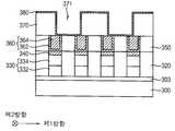
도 11 내지 도 34는 예시적인 실시예들에 따른 상변화 메모리 소자의 제조 방법을 설명하기 위한 단면도들이다. 구체적으로, 도 11, 13, 15, 17, 19, 21, 23, 25, 27, 29, 31 및 33은 상변화 메모리 소자를 제1 방향을 따라 절단한 단면도들이고, 도 12, 14, 16, 18, 20, 22, 24, 26, 28, 30 및 32는 상변화 메모리 소자를 상기 제1 방향에 실질적으로 수직한 제2 방향을 따라 절단한 단면도들이다.11 to 34 are cross-sectional views illustrating a method of manufacturing a phase change memory device according to example embodiments. Specifically, FIGS. 11, 13, 15, 17, 19, 21, 23, 25, 27, 29, 31, and 33 are cross-sectional views of cutting a phase change memory device in a first direction, and FIGS. 12, 14, 16, 18, 20, 22, 24, 26, 28, 30, and 32 are cross-sectional views of phase change memory devices cut along a second direction substantially perpendicular to the first direction.
도 11 및 도 12를 참조하면, 기판(300) 상부에 이온 주입 공정을 수행함으로써 불순물 영역을 형성한 뒤, 소자 분리막 패턴(310)을 형성하여 기판(300)을 액티브 영역과 필드 영역으로 구분하고 워드 라인들(303)을 형성한다.11 and 12, after forming an impurity region by performing an ion implantation process on the
불순물 영역은 제1 불순물 예를 들어, 인, 비소와 같은 n형 불순물 또는 붕소, 갈륨과 같은 p형 불순물을 기판(300) 상부에 주입함으로써 형성될 수 있다. 일 실시예에 있어서, 상기 제1 불순물은 n형 불순물이다. 한편, 상기 불순물 영역 하부에는 상기 제1 불순물과는 다른 도전형의 불순물이 도핑된 웰 영역(도시되지 않음)이 더 형성될 수도 있다.The impurity region may be formed by implanting a first impurity, for example, an n-type impurity such as phosphorus or arsenic or a p-type impurity such as boron or gallium on the
예시적인 실시예들에 있어서, 소자 분리막 패턴(310)은 얕은 트렌치 소자 분리(Shallow Trench Isolation: STI) 공정에 의해 형성될 수 있다. 즉, 기판(300) 상에 트렌치들(305)을 형성하고, 트렌치들(305)을 충분히 채우는 소자 분리막(도시하지 않음)을 기판(300) 상에 형성한 후, 기판(300) 상면이 노출될 때까지 상기 소자 분리막을 평탄화함으로써 형성할 수 있다. 상기 소자 분리막은 예를 들어 BPSG, PSG, USG, SOG, FOX, TEOS, PE-TEOS, HDP-CVD 산화물 등과 같은 실리콘 산화물을 사용하여 형성할 수 있다. 예시적인 실시예들에 있어서, 상기 평탄화 공정은 화학 기계적 연마(CMP) 공정 및/또는 에치 백(etch back) 공정을 통해 수행될 수 있다. 예시적인 실시예들에 있어서, 소자 분리막 패턴(310)은 기판(300) 상면에 평행한 제1 방향으로 연장되고, 상기 제1 방향에 실질적으로 수직한 제2 방향을 따라 복수 개로 형성될 수 있다. 이에 따라, 기판(300)의 상기 액티브 영역 역시 상기 제1 방향으로 연장되고 상기 제2 방향을 따라 복수 개로 형성될 수 있다.In example embodiments, the device
예시적인 실시예들에 있어서, 소자 분리막 패턴(310)은 상기 불순물 영역의 저면보다 낮은 저면을 갖도록 형성될 수 있으며, 이에 따라, 상기 액티브 영역 상부에 형성된 상기 불순물 영역이 소자 분리막 패턴(310)에 의해 분리되어 복수 개의 워드 라인들(303)을 형성할 수 있다. 예시적인 실시예들에 있어서, 각 워드 라인들(303)은 상기 제1 방향으로 연장되고, 상기 제2 방향을 따라 복수 개로 형성될 수 있다. In example embodiments, the device
도 13 및 도 14를 참조하면, 기판(300) 및 소자 분리막 패턴(310) 상에 상기 각 제1 및 제2 방향들을 따라 일정한 간격으로 배열된 복수의 제1 콘택 홀들(325)이 형성된 제1 층간 절연막(320)을 형성한다. 이때, 제1 콘택 홀들(325)은 제1 콘택 어레이를 형성할 수 있다.Referring to FIGS. 13 and 14, a plurality of first contact holes 325 are formed on the
제1 콘택 홀들(325)은 기판(300) 상에 제1 층간 절연막(320)을 형성한 뒤, 워드 라인들(303)의 상면을 노출시키도록 제1 층간 절연막(320)을 예를 들어, 이방성 식각함으로써 형성할 수 있다.The first contact holes 325 may form the first
한편, 제1 층간 절연막(320)은 예를 들어, 산화물, 질화물 등과 같은 절연 물질을 포함하도록 형성할 수 있다.Meanwhile, the first
도 15 및 도 16을 참조하면, 제1 콘택 홀들(325)을 채우는 다이오드(330) 및 오믹 패턴(340)을 순차적으로 형성한다.15 and 16, the
예시적인 실시예들에 있어서, 다이오드(330)는 기판(300)의 노출된 워드 라인들(303) 상면을 씨드막으로 사용하는 선택적 에피택시얼 공정을 수행하여 제1 콘택 홀들(325)을 채우는 실리콘막을 형성하고, 상기 실리콘막의 하부 및 상부에 각각 제2 및 제3 불순물들을 주입함으로써 형성할 수 있다. 이에 따라, 상기 실리콘막의 하부 및 상부는 각각 하부 다이오드막(332) 및 상부 다이오드막(334)으로 정의될 수 있으며, 하부 다이오드막(332)의 경우 워드 라인들(303)의 상면과 접촉할 수 있다. 한편, 상기 제2 및 제3 불순물들을 주입하기 이전에, 상기 실리콘막의 상면에 대하여 평탄화 공정을 더 수행함으로써 다이오드(330)의 상면이 제1 층간 절연막(320)의 상면과 동일한 높이를 갖도록 형성할 수 있다.In example embodiments, the
일 실시예에 있어서, 상기 제2 불순물은 예를 들어, 인, 비소와 같은 n형 불순물이고, 상기 제3 불순물은 예를 들어, 붕소, 갈륨과 같은 p형 불순물이다.In one embodiment, the second impurity is, for example, an n-type impurity such as phosphorus or arsenic, and the third impurity is, for example, a p-type impurity such as boron or gallium.
오믹 패턴(340)은 다이오드(330)와 후속하여 형성되는 콘택 플러그(360) 사이의 접촉 저항을 감소시키기 위한 것으로서, 예시적인 실시예들에 있어서 다이오드(330) 및 제1 층간 절연막(320) 상에 금속막(미도시)을 형성하고, 열처리를 통해 상기 금속막과 다이오드(330)의 실리콘 성분을 반응시킴으로써 형성할 수 있다. 상기 금속막은 예를 들어, 코발트, 니켈, 텅스텐과 같은 금속을 포함하도록 형성할 수 있으며, 이에 따라 오믹 패턴(340)은 코발트 실리사이드, 니켈 실리사이드, 텅스텐 실리사이드와 같은 금속 실리사이드를 포함하도록 형성될 수 있다. 이후 상기 금속막 중 미반응 부분은 제거한다.The
이와는 달리, 예시적인 실시예들에 있어 오믹 패턴(340)은 다이오드(330) 상부에 금속 이온을 직접 주입함으로써 형성할 수도 있으며, 경우에 따라 형성하지 않고 생략할 수도 있다.Alternatively, in the exemplary embodiments, the
한편, 다이오드(330) 및 오믹 패턴(340)은 각각 제1 콘택 홀들(325) 내에 형성되기 때문에, 상기 제1 및 제2 방향들을 따라 각각 복수 개로 형성되어 다이오드 어레이 및 오믹 패턴 어레이를 형성할 수 있다.Meanwhile, since the
도 17 및 도 18을 참조하면, 도 13 및 도 14를 참조로 설명한 공정들과 실질적으로 동일하거나 유사한 공정들을 수행함으로써, 제1 층간 절연막(320) 및 오믹 패턴들(340) 상에 상기 각 제1 및 제2 방향들을 따라 일정한 간격으로 배열된 복수 개의 제2 콘택 홀들(355)이 형성된 제2 층간 절연막(350)을 형성한다.Referring to FIGS. 17 and 18, by performing the processes substantially the same as or similar to those described with reference to FIGS. 13 and 14, the respective layers may be formed on the first
즉, 제2 콘택 홀들(355)은 제1 층간 절연막(320) 및 오믹 패턴들(340) 상에 예를 들어, 산화물, 질화물 등과 같은 절연 물질을 사용하여 제2 층간 절연막(350)을 형성한 후, 제2 층간 절연막(350)을 오믹 패턴들(340)의 상면을 노출시키도록 예를 들어, 이방성 식각함으로써 형성할 수 있다. 이때, 제2 콘택 홀들(355)은 제2 콘택 홀 어레이를 형성할 수 있다.In other words, the second contact holes 355 may be formed on the first
도 19 및 도 20을 참조하면, 제2 콘택 홀들(355)을 채우는 콘택 플러그(360)를 형성한다. 이에 따라, 콘택 플러그(360)는 상기 제1 및 제2 방향들을 따라 각각 복수 개로 형성되어 콘택 플러그 어레이를 형성할 수 있다.19 and 20, a
예시적인 실시예들에 있어서, 콘택 플러그(360)는 제2 콘택 홀들(355)에 의해 노출된 오믹 패턴들(340)의 상면, 제2 콘택 홀들(355)의 측벽 및 제2 층간 절연막(350)의 상면 상에 제1 배리어막(도시하지 않음)을 형성하고, 이어, 제2 콘택 홀들(355)의 나머지 부분을 충분히 매립하는 제1 도전막(도시하지 않음)을 상기 제1 배리어막 상에 형성한 뒤, 상기 제1 배리어막 및 제1 도전막의 상부를 제2 층간 절연막(350)의 상면이 노출될 때까지 평탄화함으로써 형성할 수 있다. 그러므로 콘택 플러그(360)는 제1 배리어막 패턴(362) 및 제1 도전막 패턴(364)을 포함하도록 형성될 수 있으며, 제1 배리어막 패턴(362)은 제1 도전막 패턴(364)의 측벽 및 저면을 감싸도록 형성될 수 있다.In example embodiments, the
상기 제1 배리어막은 예를 들어, 티타늄, 티타늄 질화물 등과 같은 금속 또는 금속 질화물을 사용하여 형성할 수 있고, 상기 제1 도전막은 예를 들어, 구리, 텅스텐, 알루미늄 등과 같은 저항 금속을 사용하여 형성할 수 있다.The first barrier layer may be formed using, for example, a metal or a metal nitride such as titanium, titanium nitride, or the like, and the first conductive layer may be formed using a resistive metal such as, for example, copper, tungsten, or aluminum. Can be.
다만, 콘택 플러그(360)는 경우에 따라 형성하지 않고 생략할 수도 있다.However, the
도 21 및 도 22를 참조하면, 콘택 플러그(360)의 상면을 부분적으로 노출시키는 제1 개구(371)를 갖는 제3 층간 절연막(370)을 제2 층간 절연막(350) 상에 형성하고, 제1 개구(371)의 측벽 및 콘택 플러그(360), 제2 층간 절연막(350) 및 제3 층간 절연막(370)의 상면 상에 하부 전극막(380)을 형성한다.21 and 22, a third
예시적인 실시예들에 있어서, 제1 개구(371)는 상기 제1 방향으로 복수 개가 형성되며, 상기 제2 방향으로 연장될 수 있다. 이때, 상기 제1 방향으로 서로 인접하는 2개의 콘택 플러그들(360)은 하나의 제1 개구(371)에 의해 노출될 수 있다.In example embodiments, a plurality of
하부 전극막(380)은 금속 화합물, 예를 들어 금속, 금속 질화물 또는 금속 실리콘 질화물을 포함하도록 형성할 수 있고, 제1 개구(371)에 의해 노출된 콘택 플러그들(360) 및 제2 층간 절연막(350)의 상면, 제1 개구(371)의 측벽 및 제3 층간 절연막(370)의 상면 상에 컨포멀하게(conformally) 형성될 수 있다.The
한편, 제3 층간 절연막(370)은 예를 들어, 산화물, 질화물 등과 같은 절연 물질을 포함하도록 형성할 수 있다.Meanwhile, the third
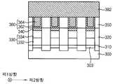
도 23 및 도 24를 참조하면, 하부 전극막(380) 상에 스페이서(400)를 형성한 뒤, 스페이서(400)를 식각 마스크로 사용하여 하부 전극막(380)을 식각함으로써 하부 전극막 패턴(382)을 형성한다.Referring to FIGS. 23 and 24, after forming the
스페이서(400)는 하부 전극막(380) 상에 스페이서막(도시하지 않음)을 형성한 후, 상기 스페이서막을 예를 들어 이방성 식각함으로써 형성할 수 있다. 이에 따라, 스페이서(400)는 제1 개구(371)의 측벽 내에 2개가 형성되며, 제1 개구(371)가 상기 제1 방향을 따라 복수 개로 형성되므로 스페이서(400) 역시 상기 제1 방향을 따라 복수 개가 형성될 수 있다.The
따라서 하부 전극막 패턴(382)도 제1 개구(371)의 측벽에 상기 제2 방향으로는 연장되고, 상기 제1 방향을 따라 복수 개가 형성될 수 있다. 이때, 하부 전극막(380)이 상술한 바와 같이 제1 개구(371)의 측벽 및 제1 개구(371)에 의해 노출된 콘택 플러그(360) 상면에 컨포멀하게 형성되기 때문에, 각 하부 전극막 패턴들(382)은 상기 제1 방향으로 절단한 단면이 L자 형상 또는 J자 유사한 형상을 가지도록 형성될 수 있다. 하부 전극막 패턴(382)이 L자 형상의 단면을 가짐에 따라, 후속하여 형성되는 상변화 물질막 패턴(470)과의 접촉 면적보다 콘택 플러그(360)와의 접촉 면적이 상대적으로 커지게 되어 작은 전류로도 상변화 물질막 패턴(470)을 효율적으로 가열할 수 있다.Accordingly, the lower
한편, 상기 스페이서막은 예를 들어, 산화물, 질화물 등과 같은 절연 물질을 포함하되, 제3 층간 절연막(370)과 실질적으로 동일한 물질을 포함하도록 형성할 수 있다.On the other hand, the spacer layer may include an insulating material such as, for example, an oxide or a nitride, and may be formed to include substantially the same material as the third
도 25 및 도 26을 참조하면, 제1 개구(371)의 나머지 부분을 충분히 채우는 제4 층간 절연막(도시하지 않음)을 노출된 콘택 플러그들(360) 및 제2 층간 절연막의(350) 상면, 스페이서들(400), 하부 전극막 패턴들(382) 및 제3 층간 절연막(370)의 상면 상에 형성하고, 하부 전극막 패턴들(382)의 상면이 노출될 때까지 이를 평탄화한다.25 and 26, an upper surface of the contact plugs 360 and the second
상기 제4 층간 절연막은 예를 들어, 산화물, 질화물 등과 같은 절연 물질을 포함하되, 제3 층간 절연막(370) 및 스페이서(400)와 실질적으로 동일한 물질을 포함하도록 형성할 수 있다. 이에 따라, 상기 제4 층간 절연막, 스페이서(400) 및 제3 층간 절연막(370)은 서로 병합될 수 있으며, 앞으로는 상기 병합된 막 구조물을 단순히 제4 층간 절연막(410)으로 통칭하기로 한다. 즉, 제4 층간 절연막(410)은 하부 전극막 패턴들(382)의 측벽을 감싸며 콘택 플러그들(360) 및 제2 층간 절연막(350) 상에 형성될 수 있다.For example, the fourth interlayer insulating layer may include an insulating material such as an oxide or a nitride, and may include a material substantially the same as that of the third
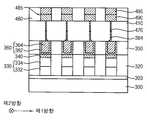
도 27 및 도 28을 참조하면, 상기 제2 방향으로 연장되는 포토레지스트 패턴(도시되지 않음)을 사용하는 식각 공정을 통해 하부 전극막 패턴(382)을 부분적으로 식각함으로써, 상기 제1 방향을 따라 복수 개의 하부 전극들(384)을 형성한다. 이때, 하부 전극막 패턴들(382)이 상기 제1 방향을 따라 복수 개로 형성되므로, 하부 전극들(384) 역시 상기 제1 방향을 따라 복수 개가 형성될 수 있으며, 이에 따라, 상기 제1 및 제2 방향들을 따라 각각 복수 개로 형성된 하부 전극들(384)을 포함하는 하부 전극 어레이가 형성될 수 있다.Referring to FIGS. 27 and 28, the lower
한편, 하부 전극막 패턴(382)을 식각할 때, 제4 층간 절연막(410)도 부분적으로 식각되어 제2 개구(도시되지 않음)가 형성될 수 있으며, 이후 상기 제2 개구를 채우는 제5 층간 절연막(420)을 형성할 수 있다.Meanwhile, when the lower
도 29 및 도 30을 참조하면, 하부 전극들(384)의 상부를 제거함으로써 리세스(415)를 형성한다.29 and 30, the
예시적인 실시예들에 있어서, 하부 전극들(384)은 습식 식각 공정을 통해 부분적으로 제거할 수 있고, 이때, 하부 전극들(384)이 상술한 바와 같이 상기 제1 및 제2 방향들을 따라 각각 복수 개로 형성되어 하부 전극 어레이를 형성하므로, 리세스(415) 역시 상기 제1 및 제2 방향들을 따라 각각 복수 개가 형성되어 리세스 어레이를 형성할 수 있다.In example embodiments, the
도 31 및 도 32를 참조하면, 앞서 상변화 물질막의 형성 방법에서 설명한 공정들과 실질적으로 동일하거나 유사한 공정들을 수행함으로써, 각 리세스들(415)을 채우는 상변화 물질막 패턴(470)을 형성한다.31 and 32, a phase change
앞서 설명한 조성의 상변화 물질막은 스퍼터링 공정, 화학 기상 증착(CVD) 공정, 사이클링 화학 기상 증착(cyclic CVD) 공정 및 원자층 증착(ALD) 공정 등과 같은 다양한 공정을 통해서 형성될 수 있다. 특히, 상기 ALD 공정을 통해서, 상기 상변화 물질막을 형성하는 경우, 각각의 소스 주입 시간 또는 각각의 소스 주입 사이클 변경을 통해서 원하는 조성의 상변화 물질막을 안정적으로 형성할 수 있다.The phase change material film of the above-described composition may be formed through various processes such as a sputtering process, a chemical vapor deposition (CVD) process, a cycling chemical vapor deposition (cyclic CVD) process, and an atomic layer deposition (ALD) process. In particular, when the phase change material film is formed through the ALD process, the phase change material film having a desired composition may be stably formed through each source injection time or each source injection cycle change.
일 실시예에 있어서, 상기 Ge 소스를 공급하는 단계, 상기 Te 소스를 공급하는 단계 및 이들 사이에 배치된 퍼지 단계를 포함하는 제1 사이클을 수행하여, GeTe를 형성하고, 상기 Ge 소스를 공급하는 단계, 상기 Sb 소스를 공급하는 단계 및 이들 사이에 배치된 퍼지 단계를 포함하는 제2 사이클을 수행하여, Sb2Te3를 형성하여, GST 물질막을 형성할 수 있다. 본 발명의 상변화 물질막의 조성의 경우, 상기 Sb가 미량으로 첨가되므로, 상기 GeTe를 형성하는 상기 제1 사이클을 수회 수행한 후, 상기 Sb2Te3를 형성하는 상기 제2 사이클을 1회 수행할 수도 있다. 또한, 불순물 소스 가스 주입 단계는 상기 제1 사이클 이후 및/또는 상기 제2 사이클 이후에 수행되어, 상기 GST 물질막 내에 불순물을 주입할 수 있다.In one embodiment, performing a first cycle comprising supplying the Ge source, supplying the Te source, and purge disposed therebetween to form GeTe and supply the Ge source. A second cycle including a step, supplying the Sb source, and a purge step disposed therebetween may be performed to form Sb2 Te3 to form a GST material film. In the case of the composition of the phase change material film of the present invention, since the Sb is added in a small amount, after performing the first cycle of forming GeTe several times, the second cycle of forming Sb2 Te3 is performed once. You may. In addition, the impurity source gas injection may be performed after the first cycle and / or after the second cycle to inject impurities into the GST material film.
도 33 내지 도 34를 참조하면, 상변화 물질막 패턴들(470)의 상면을 노출시키는 제3 개구(485)를 갖는 제6 층간 절연막(480)을 제4 및 제5 층간 절연막(410, 420) 상에 형성하고, 제3 개구(485)를 채우는 상부 전극(490) 및 비트 라인(495)을 순차적으로 형성한다.33 to 34, a sixth and fifth
상부 전극(490)은 노출된 상변화 물질막 패턴(470) 및 제4 내지 제6 층간 절연막(410, 420, 480)의 상면 상에 제3 개구(485)를 충분히 매립하도록 제2 도전막(도시하지 않음)을 형성하고, 제6 층간 절연막(480)의 상면이 노출될 때까지 상기 제2 도전막을 평탄화한 후, 평탄화된 상기 제2 도전막의 상부를 예를 들어, 습식 식각 공정을 통해 제거함으로써 형성할 수 있다. 이에 따라, 상부 전극(490)은 상변화 물질막 패턴(470)의 상면을 커버하도록 형성될 수 있다.The
이어, 이와 유사하게 상부 전극(490)의 상면 및 제6 층간 절연막(480) 상에 상기 제2 도전막 상부가 제거된 공간을 충분히 매립하도록 제3 도전막(도시하지 않음)을 형성하고, 상기 제3 도전막을 제6 층간 절연막(480)의 상면이 노출될 때까지 평탄화함으로써 비트라인(495)을 형성할 수 있다.Similarly, a third conductive film (not shown) is formed on the upper surface of the
예시적인 실시예들에 있어서, 제3 개구(485)는 상기 제1 방향을 따라 복수 개 형성되므로, 상부 전극(490)은 역시 상기 제1 방향을 따라 복수 개 형성되어 상부 전극 열을 형성할 수 있다. 그러므로 비트 라인(495) 또한 상기 제1 방향을 따라 복수 개가 형성될 수 있다.In example embodiments, since a plurality of
한편, 예시적인 실시예들에 있어서 제6 층간 절연막(480)은 산화물, 질화물 등과 같은 절연 물질을 포함하도록 형성할 수 있고, 상기 제2 도전막은 금속, 금속 질화물, 금속 실리사이드 등을 포함하도록 형성할 수 있으며, 상기 제3 도전막은 구리, 알루미늄, 텅스텐과 같은 저 저항 금속을 포함하도록 형성할 수 있다.Meanwhile, in example embodiments, the sixth
일 실시예에 있어서, 비트 라인(495)은 금속 질화물을 포함하는 배리어막 패턴(도시되지 않음)을 구비하도록 형성할 수도 있다.
In an embodiment, the
컴퓨팅 시스템Computing system
도 35는 본 발명의 실시예에 따른 컴퓨팅 시스템을 나타내는 개념도이다.35 is a conceptual diagram illustrating a computing system according to an embodiment of the present invention.
컴퓨팅 시스템(500)은 복수 개의 프로세스를 처리하는 프로세서(510), 메인 메모리(520), 메모리 제어부(Memory controller)(530) 및 저장부(Storage)(540)를 포함한다.The
메인 메모리(520)는 프로세서(510)가 처리하는 복수 개의 프로세스에 대한 컴퓨팅 연산을 위해, 저장부(540)로부터 필요한 파일을 독출하여 임시로 저장하고, 프로세스에 대한 컴퓨팅 연산의 종료 등의 원인에 의해 저장부(540)로 데이터가 옮겨지기 전까지 상기 프로세스에 대한 컴퓨팅 연산 도중의 데이터, 결과 데이터를 저장한다.The
프로세서(510)의 동작 속도는 약 1ns이지만, 저장부(540)에 사용되는 하드 디스크 읽기/쓰기 속도가 약 5ms이므로, 프로세서(510)와 저장부(540) 사이에 큰 속도의 차이(access time gap)가 존재한다. 이러한 속도 차이를 극복하기 위해서 종래에는 캐시 메모리(도시되지 않음)을 이용하지만. 상기 캐시 메모리보다 큰 용량의 데이터를 다루어야 하는 경우 위에서 언급한 문제 때문에 속도 지연이 발생한다. 또한, 약 20us의 동작 속도를 갖는 SSD와 같이 FLASH를 사용하여도 속도의 차이는 보완할 수 없다.Although the operating speed of the
한편, 종래에 휘발성 메모리, 이를테면 SRAM 또는 DRAM만을 컴퓨팅 연산의 메인 메모리로서 사용한 컴퓨팅 시스템에서는, 갑작스러운 전원 차단으로 인한 데이터 손실이 문제되었다. 따라서, 갑작스러운 전원 차단 등의 이벤트에도 데이터 손실이 없도록 하기 위해서는 추가적으로 비휘발성 램(Non-volatile RAM; NVRAM)로 적용한다.On the other hand, in a conventional computing system using only volatile memory, such as SRAM or DRAM as the main memory of a computing operation, data loss due to sudden power off has been a problem. Therefore, in order to prevent data loss even in the event of sudden power failure, it is additionally applied as non-volatile RAM (NVRAM).
본 발명의 일 실시예에 따르면, 메인 메모리(520)는 상기 복수 개의 프로세스 중 적어도 일부에 대한 컴퓨팅 연산에 있어서 메인 메모리로서 동작하는 SCM(Storage Class Memory)(521) 및 상기 복수 개의 프로세스 중 다른 일부에 대한 컴퓨팅 연산에 있어서 메인 메모리로서 동작하는 DRAM(Dynamic Random Access Memory)(522)를 포함한다. 또한, SCM(521) 및 DRAM(522)은 메모리 제어부(530)에 의해 제어될 수 있다.According to an embodiment of the present invention, the
여기서 DRAM(522)은 메인 메모리로서 동작할 수 있는 휘발성 메모리(volatile memory)의 일 예이며, 다른 종류로 대체될 수 있음은 물론이다. 한편, SCM(521)은 앞서 설명한 상변화 물질막을 이용한 비휘발성 메모리 소자를 포함한다.Here, the
SCM(521)는 앞서 설명한 고온 안정성 및 빠른 결정화 속도를 갖는 상변화 물질막을 포함한다. 즉, 상기 상변화 물질막은 약 70℃이상의 10년 보장 온도 및 100ns 이하의 결정화 속도를 가질 수 있다. 이에 따라, 상기 상변화 물질막을 포함하는 SCM(521)은 약 1us 이하의 접근 속도(단일 셀 랜덤 엑세스의 경우, 약 100ns 이하의 접근 속도)를 가질 수 있다. 이에 따라, SCM(521)은 프로세서(510)와 저장부(540) 사이의 속도 차이를 보완할 뿐만 아니라, 갑작스러운 전원 차단으로 인한 데이터 손실이 문제를 해결할 수 있다.
상술한 컴퓨팅 시스템(500)은 대용량의 데이터를 동시에 처리하며, 빠른 동작 속도 및 신뢰성을 요구하는 서버(server)에 이용될 수 있다. 즉, 상기 상변화 메모리 소자를 상기 서버에 이용하는 경우, 프로세서(510)와 저장부(540) 사이의 속도 차이를 보완하여 보다 빨리 데이터를 처리할 수 있다. 또한, 일시적인 오류 또는 전원 차단에 의해서도 상기 상변화 메모리 소자 내의 정보가 보존될 수 있으며, 우수한 리텐션 특성으로 인해서 보다 높은 온도에서도 안정적으로 작동할 수 있다. 또한, 리텐션 특성으로 인해서, DRAM과 같은 리플레싱 작업이 생략될 수도 있다.
The above-described
100, 300: 기판103, 303: 워드 라인
305: 트렌치110, 310: 소자 분리막 패턴
120, 320: 제1 층간 절연막 325: 제1 콘택 홀
130, 330: 다이오드 132, 332: 하부 다이오드
134, 334: 상부 다이오드140, 340: 오믹
150, 350: 제2 층간 절연막355: 제2 콘택 홀
160, 360: 콘택 플러그162, 362: 제1 배리어막 패턴
164, 364: 제1 도전막 패턴370: 제3 층간 절연막
371: 제1 개구380: 하부 전극막
382: 하부 전극막 패턴184, 384: 하부 전극
400: 스페이서210, 410: 제4 층간 절연막
415: 리세스420: 제5 층간 절연막
270, 470: 상변화 물질막 패턴480: 제6 층간 절연막
485: 제3 개구290, 490: 상부 전극
295, 495: 비트 라인500: 컴퓨팅 시스템
510: 프로세서520: 메인 메모리
530: 메모리 제어부540: 저장부100, 300:
305:
120 and 320: first interlayer insulating film 325: first contact hole
130, 330:
134, 334:
150 and 350: second interlayer insulating film 355: second contact hole
160 and 360: contact plugs 162 and 362: first barrier film pattern
164 and 364: first conductive film pattern 370: third interlayer insulating film
371: First Opening 380: Lower Electrode Film
382: lower
400:
415: recess 420: fifth interlayer insulating film
270 and 470: Phase change material film pattern 480: Sixth interlayer insulating film
485:
295, 495: bit line 500: computing system
510: processor 520: main memory
530: memory control unit 540: storage unit
Claims (10)
Translated fromKorean상기 불순물의 원자 농도 a는 0 < a ≤ 0.25이고,
상기 안티몬의 원자 농도 c는 0.03 < c ≤ 0.15이며,
상기 상변화 물질막은 결정화 온도 이상에서 GeTe 및 Ge2Sb2Te5보다 빠른 속도로 결정화 되는 것을 특징으로 하는 상변화 물질막.A phase change material film containing germanium (Ge), antimony (Sb), tellurium (Te), and at least one impurity,
The atomic concentration a of the impurity is 0 <a ≦ 0.25,
The atomic concentration c of the antimony is 0.03 <c ≤ 0.15,
The phase change material film is a phase change material film, characterized in that the crystallization faster than GeTe and Ge2 Sb2 Te5 above the crystallization temperature.
상기 제1 불순물의 원자 농도 a1과 상기 제2 불순물의 원자 농도 a2의 합은 0 < a1+a2≤ 0.2인 것을 특징으로 하는 상변화 물질막.The method of claim 1, wherein the impurities include a first impurity and a second impurity selected from boron, carbon, nitrogen, oxygen, aluminum, silicon, phosphorus, and sulfur,
The sum of the atomic concentration a1 of the first impurity and the atomic concentration a2 of the second impurity is 0 <a1 + a2 ≤ 0.2.
상기 상변화 물질막은 70℃ 이하의 온도에서 10년 이상 비정질 상태를 유지하며,
상기 상변화 물질막은 결정화 온도 이상에서 GeTe 및 Ge2Sb2Te5보다 빠른 속도로 결정화되는 것을 특징으로 하는 상변화 물질막.A phase change material film containing germanium (Ge), antimony (Sb), tellurium (Te), and at least one impurity,
The phase change material film maintains an amorphous state for more than 10 years at a temperature of 70 ℃ or less,
The phase change material film is a phase change material film, characterized in that the crystallization faster than GeTe and Ge2 Sb2 Te5 above the crystallization temperature.
안티몬(Sb)의 원자 농도가 0.03인 조성을 연결하는 제1 조성선;
안티몬(Sb)의 원자 농도가 0.15인 조성을 연결하는 제2 조성선;
게르마늄(Ge)의 원자 농도가 0.3인 조성을 연결하는 제3 조성선; 및
게르마늄(Ge)의 원자 농도가 0.55인 조성을 연결하는 제4 조성선에 의해서 둘러싸인 영역의 조성을포함하는 상변화 물질막으로서,
상기 상변화 물질막은 적어도 하나 이상의 불순물을 더 포함하고,
상기 상변화 물질막은 결정화 온도 이상에서 GeTe 및 Ge2Sb2Te5보다 빠른 속도로 결정화 되는 것을 특징으로 하는 상변화 물질막.In the ternary state diagram of germanium (Ge), antimony (Sb) and tellurium (Te),
A first composition line connecting a composition having an atomic concentration of antimony (Sb) of 0.03;
A second composition line connecting the composition having an atomic concentration of antimony (Sb) of 0.15;
A third composition line connecting the composition in which the atomic concentration of germanium (Ge) is 0.3; And
A phase change material film containing a composition of a region surrounded by a fourth composition line connecting a composition having an atomic concentration of germanium (Ge) of 0.55,
The phase change material film further includes at least one impurity,
The phase change material film is a phase change material film, characterized in that the crystallization faster than GeTe and Ge2 Sb2 Te5 above the crystallization temperature.
상기 반응 챔버 내에 텔루륨(Te)을 포함하는 제2 소스를 공급하는 단계 및 안티몬(Sb)를 포함하는 제3 소스를 공급하는 단계를 포함하며, 기판 상에 Sb2Te3박막을 형성하는 제2 사이클을 수행하는 제2 단계를 포함하고,
상기 제1 사이클 또는 상기 제2 사이클은 불순물 소스 가스를 공급하는 단계를 포함하며,
상기 제1 및 제2 단계들을 통해 형성되는 상변화 물질막은 결정화 온도 이상에서 GeTe 및 Ge2Sb2Te5보다 빠른 속도로 결정화 되는 것을 특징으로 하는 상변화 물질막의 형성 방법.Supplying a first source containing germanium (Ge) and supplying a second source containing tellurium (Te) in a reaction chamber, and performing a first cycle of forming a GeTe thin film on a substrate. A first step of doing; And
Supplying a second source comprising tellurium (Te) into the reaction chamber and supplying a third source comprising antimony (Sb), the second source of forming a Sb2 Te3 thin film on a substrate; A second step of performing two cycles,
The first cycle or the second cycle comprises supplying an impurity source gas,
And the phase change material film formed through the first and second steps is crystallized at a faster rate than GeTe and Ge2 Sb2 Te5 above the crystallization temperature.
Priority Applications (2)
| Application Number | Priority Date | Filing Date | Title |
|---|---|---|---|
| KR1020130092857AKR102077641B1 (en) | 2013-08-06 | 2013-08-06 | Phase-change material layer and method of manufacturing the same |
| US14/259,594US9614152B2 (en) | 2013-08-06 | 2014-04-23 | Phase change material layers |
Applications Claiming Priority (1)
| Application Number | Priority Date | Filing Date | Title |
|---|---|---|---|
| KR1020130092857AKR102077641B1 (en) | 2013-08-06 | 2013-08-06 | Phase-change material layer and method of manufacturing the same |
Publications (2)
| Publication Number | Publication Date |
|---|---|
| KR20150017066A KR20150017066A (en) | 2015-02-16 |
| KR102077641B1true KR102077641B1 (en) | 2020-02-14 |
Family
ID=52447839
Family Applications (1)
| Application Number | Title | Priority Date | Filing Date |
|---|---|---|---|
| KR1020130092857AActiveKR102077641B1 (en) | 2013-08-06 | 2013-08-06 | Phase-change material layer and method of manufacturing the same |
Country Status (2)
| Country | Link |
|---|---|
| US (1) | US9614152B2 (en) |
| KR (1) | KR102077641B1 (en) |
Families Citing this family (11)
| Publication number | Priority date | Publication date | Assignee | Title |
|---|---|---|---|---|
| KR102212377B1 (en)* | 2014-06-16 | 2021-02-04 | 삼성전자주식회사 | Method of manufacturing a phase-change memory device |
| KR102304301B1 (en) | 2014-12-23 | 2021-09-23 | 삼성전자주식회사 | Resistance-change material layer and phase-change memory device including the same |
| KR102465967B1 (en) | 2016-02-22 | 2022-11-10 | 삼성전자주식회사 | Memory device and method for fabricating the same |
| KR102483704B1 (en)* | 2016-03-30 | 2023-01-02 | 삼성전자주식회사 | Variable resistance memory devices and methods of manufacturing the same |
| US11182437B2 (en) | 2017-10-26 | 2021-11-23 | International Business Machines Corporation | Hybrid processing of disjunctive and conjunctive conditions of a search query for a similarity search |
| US10141503B1 (en)* | 2017-11-03 | 2018-11-27 | International Business Machines Corporation | Selective phase change material growth in high aspect ratio dielectric pores for semiconductor device fabrication |
| DE102018107038B4 (en)* | 2017-11-09 | 2022-06-09 | Taiwan Semiconductor Manufacturing Co., Ltd. | METHOD OF MANUFACTURING A THROUGH-PHERE STRUCTURE |
| US20210202839A1 (en)* | 2018-07-10 | 2021-07-01 | National Institute Of Advanced Industrial Science And Technology | Stacked structure and method of manufacturing same, and semiconductor device |
| CN110335941B (en)* | 2019-07-03 | 2023-08-18 | 芯盟科技有限公司 | Phase change memory structure and forming method thereof |
| CN114203901B (en)* | 2021-12-07 | 2025-05-13 | 中国科学院上海微系统与信息技术研究所 | A switch device and memory |
| US12185647B2 (en) | 2022-03-21 | 2024-12-31 | Samsung Electronics Co., Ltd. | Variable resistance memory device |
Citations (2)
| Publication number | Priority date | Publication date | Assignee | Title |
|---|---|---|---|---|
| WO2011003803A1 (en) | 2009-07-06 | 2011-01-13 | Imec | Method for forming mems variable capacitors |
| US20120326111A1 (en) | 2011-06-23 | 2012-12-27 | Macronix International Co., Ltd. | Ge-RICH GST-212 PHASE CHANGE MEMORY MATERIALS |
Family Cites Families (20)
| Publication number | Priority date | Publication date | Assignee | Title |
|---|---|---|---|---|
| US5534712A (en) | 1991-01-18 | 1996-07-09 | Energy Conversion Devices, Inc. | Electrically erasable memory elements characterized by reduced current and improved thermal stability |
| JP3570169B2 (en) | 1997-08-22 | 2004-09-29 | 松下電器産業株式会社 | Optical information recording medium |
| KR100586875B1 (en) | 1997-12-11 | 2006-06-07 | 코닌클리케 필립스 일렉트로닉스 엔.브이. | Rewritable Optical Information Media |
| US7151273B2 (en) | 2002-02-20 | 2006-12-19 | Micron Technology, Inc. | Silver-selenide/chalcogenide glass stack for resistance variable memory |
| KR100618879B1 (en) | 2004-12-27 | 2006-09-01 | 삼성전자주식회사 | Germanium precursor, UST thin film formed using the same, method for manufacturing the thin film and phase change memory device |
| US20070034850A1 (en) | 2005-08-09 | 2007-02-15 | Ovonyx, Inc. | Chalcogenide devices incorporating chalcogenide materials having reduced germanium or telluruim content |
| US7233054B1 (en) | 2005-11-29 | 2007-06-19 | Korea Institute Of Science And Technology | Phase change material and non-volatile memory device using the same |
| KR20080016120A (en)* | 2006-08-17 | 2008-02-21 | 삼성전자주식회사 | Phase change memory device and manufacturing method thereof |
| KR100807230B1 (en) | 2006-09-27 | 2008-02-28 | 삼성전자주식회사 | Phase change material layer and phase change memory device including the same |
| KR100829601B1 (en) | 2006-09-27 | 2008-05-14 | 삼성전자주식회사 | Chalcogen compound target, manufacturing method thereof and manufacturing method of phase change memory device |
| KR100829602B1 (en)* | 2006-10-20 | 2008-05-14 | 삼성전자주식회사 | Phase change material layer formation method and phase change memory device manufacturing method |
| CN102352488B (en)* | 2006-11-02 | 2016-04-06 | 诚实公司 | The antimony useful for the CVD/ALD of metallic film and germanium complexes |
| KR101370275B1 (en)* | 2007-08-21 | 2014-03-05 | 삼성전자주식회사 | Phase Change Random Access Memory and Manufacturing Method for the Same |
| KR20090036771A (en)* | 2007-10-10 | 2009-04-15 | 삼성전자주식회사 | Method of manufacturing a phase change memory device having a doped phase change material film |
| WO2010065874A2 (en) | 2008-12-05 | 2010-06-10 | Atmi | High concentration nitrogen-containing germanium telluride based memory devices and processes of making |
| KR20160084491A (en) | 2009-05-22 | 2016-07-13 | 엔테그리스, 아이엔씨. | Low temperature gst process |
| KR101535462B1 (en)* | 2009-08-27 | 2015-07-09 | 삼성전자주식회사 | A nonvolatile memory device comprising a phase change material |
| US8685291B2 (en) | 2009-10-13 | 2014-04-01 | Ovonyx, Inc. | Variable resistance materials with superior data retention characteristics |
| TW201132787A (en)* | 2010-03-26 | 2011-10-01 | Advanced Tech Materials | Germanium antimony telluride materials and devices incorporating same |
| KR101812687B1 (en)* | 2011-06-13 | 2017-12-27 | 삼성전자주식회사 | Method for forming resistance variable memory device |
- 2013
- 2013-08-06KRKR1020130092857Apatent/KR102077641B1/enactiveActive
- 2014
- 2014-04-23USUS14/259,594patent/US9614152B2/enactiveActive
Patent Citations (2)
| Publication number | Priority date | Publication date | Assignee | Title |
|---|---|---|---|---|
| WO2011003803A1 (en) | 2009-07-06 | 2011-01-13 | Imec | Method for forming mems variable capacitors |
| US20120326111A1 (en) | 2011-06-23 | 2012-12-27 | Macronix International Co., Ltd. | Ge-RICH GST-212 PHASE CHANGE MEMORY MATERIALS |
Also Published As
| Publication number | Publication date |
|---|---|
| US20150041747A1 (en) | 2015-02-12 |
| KR20150017066A (en) | 2015-02-16 |
| US9614152B2 (en) | 2017-04-04 |
Similar Documents
| Publication | Publication Date | Title |
|---|---|---|
| KR102077641B1 (en) | Phase-change material layer and method of manufacturing the same | |
| US8901009B2 (en) | Methods of manufacturing semiconductor devices | |
| US8039828B2 (en) | Semiconductor device and method of fabricating the same | |
| US9118003B2 (en) | Variable resistance memory devices and method of forming the same | |
| US10892410B2 (en) | Variable resistance memory devices and methods of manufacturing variable resistance memory devices | |
| US20100190321A1 (en) | METHOD OF FABRICATING PHASE-CHANGE MEMORY DEVICE HAVING TiC LAYER | |
| KR20110009545A (en) | Method for forming semiconductor device having metal carbide electrode and related semiconductor device | |
| US8981330B2 (en) | Thermally-confined spacer PCM cells | |
| KR20120053328A (en) | Resistance variable memory device and method for forming the same | |
| KR101525588B1 (en) | Method of manufacturing semiconductor device | |
| KR102212377B1 (en) | Method of manufacturing a phase-change memory device | |
| US20190013357A1 (en) | Semiconductor device and method for fabricating the same | |
| US8853660B2 (en) | Semiconductor memory devices having lower and upper interconnections, selection components and memory components | |
| KR102304301B1 (en) | Resistance-change material layer and phase-change memory device including the same | |
| US20120009731A1 (en) | Method of manufacturing phase-change random access memory | |
| KR20130087196A (en) | Method for manufacturing phase-change random access memory device and method of manufacturing the same | |
| US20100124800A1 (en) | Variable resistance memory device, method of fabricating the same, and memory system including the same | |
| US9012877B2 (en) | Semiconductor device including a diode and method of manufacturing the same | |
| US11177320B2 (en) | Variable resistance memory device and method of fabricating the same | |
| US12426519B2 (en) | Memory devices | |
| US11950434B2 (en) | Memory device for reducing thermal crosstalk |
Legal Events
| Date | Code | Title | Description |
|---|---|---|---|
| PA0109 | Patent application | Patent event code:PA01091R01D Comment text:Patent Application Patent event date:20130806 | |
| PG1501 | Laying open of application | ||
| A201 | Request for examination | ||
| PA0201 | Request for examination | Patent event code:PA02012R01D Patent event date:20180529 Comment text:Request for Examination of Application Patent event code:PA02011R01I Patent event date:20130806 Comment text:Patent Application | |
| E902 | Notification of reason for refusal | ||
| PE0902 | Notice of grounds for rejection | Comment text:Notification of reason for refusal Patent event date:20190508 Patent event code:PE09021S01D | |
| E701 | Decision to grant or registration of patent right | ||
| PE0701 | Decision of registration | Patent event code:PE07011S01D Comment text:Decision to Grant Registration Patent event date:20191126 | |
| GRNT | Written decision to grant | ||
| PR0701 | Registration of establishment | Comment text:Registration of Establishment Patent event date:20200210 Patent event code:PR07011E01D | |
| PR1002 | Payment of registration fee | Payment date:20200211 End annual number:3 Start annual number:1 | |
| PG1601 | Publication of registration | ||
| PR1001 | Payment of annual fee | Payment date:20240125 Start annual number:5 End annual number:5 |