KR102075992B1 - Semiconductor Light Emitting Device - Google Patents
Semiconductor Light Emitting DeviceDownload PDFInfo
- Publication number
- KR102075992B1 KR102075992B1KR1020130123797AKR20130123797AKR102075992B1KR 102075992 B1KR102075992 B1KR 102075992B1KR 1020130123797 AKR1020130123797 AKR 1020130123797AKR 20130123797 AKR20130123797 AKR 20130123797AKR 102075992 B1KR102075992 B1KR 102075992B1
- Authority
- KR
- South Korea
- Prior art keywords
- layer
- light emitting
- emitting device
- current blocking
- transparent electrode
- Prior art date
- Legal status (The legal status is an assumption and is not a legal conclusion. Google has not performed a legal analysis and makes no representation as to the accuracy of the status listed.)
- Active
Links
Images


Classifications
- H—ELECTRICITY
- H10—SEMICONDUCTOR DEVICES; ELECTRIC SOLID-STATE DEVICES NOT OTHERWISE PROVIDED FOR
- H10H—INORGANIC LIGHT-EMITTING SEMICONDUCTOR DEVICES HAVING POTENTIAL BARRIERS
- H10H20/00—Individual inorganic light-emitting semiconductor devices having potential barriers, e.g. light-emitting diodes [LED]
- H10H20/80—Constructional details
- H10H20/83—Electrodes
- H10H20/832—Electrodes characterised by their material
- H—ELECTRICITY
- H10—SEMICONDUCTOR DEVICES; ELECTRIC SOLID-STATE DEVICES NOT OTHERWISE PROVIDED FOR
- H10H—INORGANIC LIGHT-EMITTING SEMICONDUCTOR DEVICES HAVING POTENTIAL BARRIERS
- H10H20/00—Individual inorganic light-emitting semiconductor devices having potential barriers, e.g. light-emitting diodes [LED]
- H10H20/80—Constructional details
- H10H20/83—Electrodes
- H10H20/831—Electrodes characterised by their shape
- H—ELECTRICITY
- H01—ELECTRIC ELEMENTS
- H01L—SEMICONDUCTOR DEVICES NOT COVERED BY CLASS H10
- H01L2224/00—Indexing scheme for arrangements for connecting or disconnecting semiconductor or solid-state bodies and methods related thereto as covered by H01L24/00
- H01L2224/01—Means for bonding being attached to, or being formed on, the surface to be connected, e.g. chip-to-package, die-attach, "first-level" interconnects; Manufacturing methods related thereto
- H01L2224/42—Wire connectors; Manufacturing methods related thereto
- H01L2224/47—Structure, shape, material or disposition of the wire connectors after the connecting process
- H01L2224/48—Structure, shape, material or disposition of the wire connectors after the connecting process of an individual wire connector
- H01L2224/4805—Shape
- H01L2224/4809—Loop shape
- H01L2224/48091—Arched
- H—ELECTRICITY
- H01—ELECTRIC ELEMENTS
- H01L—SEMICONDUCTOR DEVICES NOT COVERED BY CLASS H10
- H01L2224/00—Indexing scheme for arrangements for connecting or disconnecting semiconductor or solid-state bodies and methods related thereto as covered by H01L24/00
- H01L2224/01—Means for bonding being attached to, or being formed on, the surface to be connected, e.g. chip-to-package, die-attach, "first-level" interconnects; Manufacturing methods related thereto
- H01L2224/42—Wire connectors; Manufacturing methods related thereto
- H01L2224/47—Structure, shape, material or disposition of the wire connectors after the connecting process
- H01L2224/48—Structure, shape, material or disposition of the wire connectors after the connecting process of an individual wire connector
- H01L2224/481—Disposition
- H01L2224/48151—Connecting between a semiconductor or solid-state body and an item not being a semiconductor or solid-state body, e.g. chip-to-substrate, chip-to-passive
- H01L2224/48221—Connecting between a semiconductor or solid-state body and an item not being a semiconductor or solid-state body, e.g. chip-to-substrate, chip-to-passive the body and the item being stacked
- H01L2224/48225—Connecting between a semiconductor or solid-state body and an item not being a semiconductor or solid-state body, e.g. chip-to-substrate, chip-to-passive the body and the item being stacked the item being non-metallic, e.g. insulating substrate with or without metallisation
- H01L2224/48227—Connecting between a semiconductor or solid-state body and an item not being a semiconductor or solid-state body, e.g. chip-to-substrate, chip-to-passive the body and the item being stacked the item being non-metallic, e.g. insulating substrate with or without metallisation connecting the wire to a bond pad of the item
- H—ELECTRICITY
- H01—ELECTRIC ELEMENTS
- H01L—SEMICONDUCTOR DEVICES NOT COVERED BY CLASS H10
- H01L2224/00—Indexing scheme for arrangements for connecting or disconnecting semiconductor or solid-state bodies and methods related thereto as covered by H01L24/00
- H01L2224/01—Means for bonding being attached to, or being formed on, the surface to be connected, e.g. chip-to-package, die-attach, "first-level" interconnects; Manufacturing methods related thereto
- H01L2224/42—Wire connectors; Manufacturing methods related thereto
- H01L2224/47—Structure, shape, material or disposition of the wire connectors after the connecting process
- H01L2224/48—Structure, shape, material or disposition of the wire connectors after the connecting process of an individual wire connector
- H01L2224/481—Disposition
- H01L2224/48151—Connecting between a semiconductor or solid-state body and an item not being a semiconductor or solid-state body, e.g. chip-to-substrate, chip-to-passive
- H01L2224/48221—Connecting between a semiconductor or solid-state body and an item not being a semiconductor or solid-state body, e.g. chip-to-substrate, chip-to-passive the body and the item being stacked
- H01L2224/48225—Connecting between a semiconductor or solid-state body and an item not being a semiconductor or solid-state body, e.g. chip-to-substrate, chip-to-passive the body and the item being stacked the item being non-metallic, e.g. insulating substrate with or without metallisation
- H01L2224/48237—Connecting between a semiconductor or solid-state body and an item not being a semiconductor or solid-state body, e.g. chip-to-substrate, chip-to-passive the body and the item being stacked the item being non-metallic, e.g. insulating substrate with or without metallisation connecting the wire to a die pad of the item
- H—ELECTRICITY
- H01—ELECTRIC ELEMENTS
- H01L—SEMICONDUCTOR DEVICES NOT COVERED BY CLASS H10
- H01L2224/00—Indexing scheme for arrangements for connecting or disconnecting semiconductor or solid-state bodies and methods related thereto as covered by H01L24/00
- H01L2224/01—Means for bonding being attached to, or being formed on, the surface to be connected, e.g. chip-to-package, die-attach, "first-level" interconnects; Manufacturing methods related thereto
- H01L2224/42—Wire connectors; Manufacturing methods related thereto
- H01L2224/47—Structure, shape, material or disposition of the wire connectors after the connecting process
- H01L2224/48—Structure, shape, material or disposition of the wire connectors after the connecting process of an individual wire connector
- H01L2224/484—Connecting portions
- H01L2224/48463—Connecting portions the connecting portion on the bonding area of the semiconductor or solid-state body being a ball bond
- H01L2224/48465—Connecting portions the connecting portion on the bonding area of the semiconductor or solid-state body being a ball bond the other connecting portion not on the bonding area being a wedge bond, i.e. ball-to-wedge, regular stitch
- H—ELECTRICITY
- H01—ELECTRIC ELEMENTS
- H01L—SEMICONDUCTOR DEVICES NOT COVERED BY CLASS H10
- H01L2224/00—Indexing scheme for arrangements for connecting or disconnecting semiconductor or solid-state bodies and methods related thereto as covered by H01L24/00
- H01L2224/01—Means for bonding being attached to, or being formed on, the surface to be connected, e.g. chip-to-package, die-attach, "first-level" interconnects; Manufacturing methods related thereto
- H01L2224/42—Wire connectors; Manufacturing methods related thereto
- H01L2224/47—Structure, shape, material or disposition of the wire connectors after the connecting process
- H01L2224/49—Structure, shape, material or disposition of the wire connectors after the connecting process of a plurality of wire connectors
- H01L2224/491—Disposition
- H01L2224/49105—Connecting at different heights
- H01L2224/49107—Connecting at different heights on the semiconductor or solid-state body
- H—ELECTRICITY
- H01—ELECTRIC ELEMENTS
- H01L—SEMICONDUCTOR DEVICES NOT COVERED BY CLASS H10
- H01L2224/00—Indexing scheme for arrangements for connecting or disconnecting semiconductor or solid-state bodies and methods related thereto as covered by H01L24/00
- H01L2224/73—Means for bonding being of different types provided for in two or more of groups H01L2224/10, H01L2224/18, H01L2224/26, H01L2224/34, H01L2224/42, H01L2224/50, H01L2224/63, H01L2224/71
- H01L2224/732—Location after the connecting process
- H01L2224/73251—Location after the connecting process on different surfaces
- H01L2224/73265—Layer and wire connectors
- H—ELECTRICITY
- H01—ELECTRIC ELEMENTS
- H01L—SEMICONDUCTOR DEVICES NOT COVERED BY CLASS H10
- H01L2924/00—Indexing scheme for arrangements or methods for connecting or disconnecting semiconductor or solid-state bodies as covered by H01L24/00
- H01L2924/15—Details of package parts other than the semiconductor or other solid state devices to be connected
- H01L2924/181—Encapsulation
- H—ELECTRICITY
- H10—SEMICONDUCTOR DEVICES; ELECTRIC SOLID-STATE DEVICES NOT OTHERWISE PROVIDED FOR
- H10H—INORGANIC LIGHT-EMITTING SEMICONDUCTOR DEVICES HAVING POTENTIAL BARRIERS
- H10H20/00—Individual inorganic light-emitting semiconductor devices having potential barriers, e.g. light-emitting diodes [LED]
- H10H20/80—Constructional details
- H10H20/81—Bodies
- H10H20/816—Bodies having carrier transport control structures, e.g. highly-doped semiconductor layers or current-blocking structures
- H10H20/8162—Current-blocking structures
Landscapes
- Led Devices (AREA)
Abstract
Translated fromKoreanDescription
Translated fromKorean본 발명은 반도체 발광소자에 관한 것이다.
The present invention relates to a semiconductor light emitting device.
발광 다이오드는 전기에너지를 이용하여 소자 내에 포함되어 있는 물질이 빛을 발광하는 소자로서, 접합된 반도체의 전자와 정공이 재결합하며 발생하는 에너지를 광으로 변환하여 방출한다. 이러한 발광 다이오드는 현재 조명, 표시장치 및 광원으로서 널리 이용되며 그 개발이 가속화되고 있는 추세이다.
A light emitting diode is a device in which a material included in a device emits light by using electrical energy. The light emitting diode converts and generates energy generated by recombination of electrons and holes in the bonded semiconductor. Such light emitting diodes are widely used as lighting, display devices, and light sources, and their development is being accelerated.
특히, 최근 그 개발 및 사용이 활성화된 질화갈륨(GaN)계 발광 다이오드를 이용한 휴대폰 키패드, 턴 시그널 램프, 카메라 플래쉬 등의 상용화에 힘입어, 최근 발광 다이오드를 이용한 일반 조명 개발이 활기를 띠고 있다. 대형 TV의 백라이트 유닛 및 자동차 전조등, 일반 조명 등 그의 응용제품과 같이, 발광소자의 용도가 점차 대형화, 고출력화, 고효율화된 제품으로 진행하고 있으므로 이와 같은 용도에 사용되는 발광소자의 광추출 효율을 향상시키기 위한 방법이 요청되고 있다.
In particular, the development of general lighting using light emitting diodes has recently been fueled by the commercialization of mobile phone keypads, turn signal lamps, and camera flashes using gallium nitride (GaN) based light emitting diodes, which have been actively developed and used. Like the backlight units of large TVs, automotive headlamps, and general lighting, the use of light emitting devices is gradually increasing in size, high output, and high efficiency, so that light extraction efficiency of light emitting devices used in such applications is improved. There is a need for a method to do this.
당 기술분야에서는, 광추출 효율이 더욱 향상된 반도체 발광소자가 요청되고 있다.
In the art, there is a demand for a semiconductor light emitting device having further improved light extraction efficiency.
본 발명의 일 실시형태에 의한 반도체 발광소자는 제1 도전형 반도체층, 활성층 및 제2 도전형 반도체층이 순차적으로 적층된 발광구조물; 및 상기 제1 및 제2 도전형 반도체층과 각각 전기적으로 연결된 제1 및 제2 전극;을 포함하며, 상기 제2 전극은, 상기 제2 도전형 반도체층의 상면 중 일 영역에 형성된 전류차단층; 상기 전류 차단층 상에 형성된 반사부; 상기 반사부와 이격되어 배치되고, 상기 반사부를 둘러싸는 개구부를 가지며 상기 제2 도전형 반도체층 상에 형성되는 투명전극층; 상기 반사부를 덮으며 상기 투명전극층과 이격되어 형성되고 상기 전류차단층의 영역 내에 형성된 패드 전극부; 및 상기 패드 전극부로부터 일 방향으로 연장되어 형성되며 적어도 일부는 상기 투명전극층 상에 형성되는 적어도 하나의 핑거 전극부;를 포함하는 것을 특징으로 한다.A semiconductor light emitting device according to an embodiment of the present invention includes a light emitting structure in which the first conductive semiconductor layer, the active layer and the second conductive semiconductor layer are sequentially stacked; And first and second electrodes electrically connected to the first and second conductivity-type semiconductor layers, respectively, wherein the second electrode is a current blocking layer formed on one region of an upper surface of the second conductivity-type semiconductor layer. ; A reflector formed on the current blocking layer; A transparent electrode layer disposed to be spaced apart from the reflecting portion and having an opening surrounding the reflecting portion and formed on the second conductive semiconductor layer; A pad electrode portion covering the reflecting portion and spaced apart from the transparent electrode layer and formed in an area of the current blocking layer; And at least one finger electrode portion extending from the pad electrode portion in one direction and at least part of which is formed on the transparent electrode layer.
상기 투명전극층은 적어도 일부 영역이 상기 전류차단층과 접할 수 있다.At least a portion of the transparent electrode layer may contact the current blocking layer.
상기 패드 전극부는 상기 개구부의 측면과 일정간격 이격되어 형성될 수 있다.The pad electrode portion may be formed spaced apart from the side surface of the opening.
상기 패드 전극부와 상기 투명전극층을 전기적으로 연결하는 연결부를 더 포함할 수 있다.The display device may further include a connection part electrically connecting the pad electrode part and the transparent electrode layer.
상기 연결부는 소정 길이로 절단된 형태로 형성되되, 상기 연결부의 일단은 상기 투명전극층 상에 배치되며 타단은 상기 패드 전극부 상에 배치될 수 있다.The connection part may be formed in a shape cut into a predetermined length, one end of the connection part may be disposed on the transparent electrode layer, and the other end may be disposed on the pad electrode part.
상기 연결부는 인접한 상기 핑거 전극부와 이격된 간격이 최대가 되는 영역에 배치될 수 있다.The connection part may be disposed in an area where the distance from the adjacent finger electrode part is maximized.
상기 연결부는 복수개가 형성될 수 있다.A plurality of connection parts may be formed.
상기 복수개의 연결부는 인접한 상기 핑거 전극부과 서로 동일 간격으로 이격될 수 있다.The plurality of connection parts may be spaced apart from each other with the adjacent finger electrode parts at equal intervals.
상기 연결부는 상기 핑거 전극부보다 짧은 길이로 형성될 수 있다.
The connection part may be formed to have a shorter length than the finger electrode part.
본 발명의 다른 실시형태에 의한 반도체 발광소자는 제1 도전형 반도체층, 활성층 및 제2 도전형 반도체층이 순차적으로 적층된 발광구조물; 및 상기 제1 및 제2 도전형 반도체층과 각각 전기적으로 연결된 제1 및 제2 전극;을 포함하며, 상기 제2 전극은, 상기 제2 도전형 반도체층의 상면 중 일 영역에 형성된 전류차단층; 상기 전류 차단층 상에 형성된 반사부; 상기 전류차단층과 이격되어 배치되고, 상기 전류차단층을 둘러싸는 개구부를 가지며 상기 제2 도전형 반도체층 상에 형성되는 투명전극층; 상기 반사부를 덮으며 상기 투명전극층과 이격되어 형성되고 상기 전류차단층의 영역 내에 형성된 패드 전극부; 및 상기 패드 전극부로부터 일 방향으로 연장되어 형성되며 적어도 일부는 상기 투명전극층 상에 형성되는 적어도 하나의 핑거 전극부;를 포함하는 것을 특징으로 한다.
A semiconductor light emitting device according to another embodiment of the present invention includes a light emitting structure in which the first conductive semiconductor layer, the active layer and the second conductive semiconductor layer are sequentially stacked; And first and second electrodes electrically connected to the first and second conductivity-type semiconductor layers, respectively, wherein the second electrode is a current blocking layer formed on one region of an upper surface of the second conductivity-type semiconductor layer. ; A reflector formed on the current blocking layer; A transparent electrode layer disposed to be spaced apart from the current blocking layer and having an opening surrounding the current blocking layer and formed on the second conductive semiconductor layer; A pad electrode portion covering the reflecting portion and spaced apart from the transparent electrode layer and formed in an area of the current blocking layer; And at least one finger electrode portion extending from the pad electrode portion in one direction and at least part of which is formed on the transparent electrode layer.
본 발명의 일 실시형태에 의한 반도체 발광소자는 반도체 발광소자의 광추출 효율이 더욱 향상되는 효과가 있다.
The semiconductor light emitting device according to the embodiment of the present invention has an effect of further improving the light extraction efficiency of the semiconductor light emitting device.
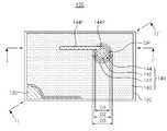
도 1은 본 발명의 일 실시형태에 의한 반도체 발광소자의 평면도이다.
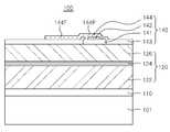
도 2는 도 1의 반도체 발광소자를 I-I'축을 따라 절개한 측단면도이다.
도 3은 도 1의 반도체 발광소자를 II-II'축을 따라 절개한 측단면도이다.
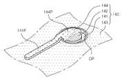
도 4는 도 1의 제2 전극부를 부분절개한 사시도이다.
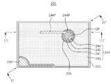
도 5는 본 발명의 다른 실시형태에 의한 반도체 발광소자의 평면도이다.
도 6은 도 5의 반도체 발광소자를 III-III'축을 따라 절개한 측단면도이다.
도 7은 도 5의 반도체 발광소자를 IV-IV'축을 따라 절개한 측단면도이다.
도 8은 도 1의 반도체 발광소자의 변형예의 평면도이다.
도 9는 본 발명의 일 실시형태에 의한 반도체 발광소자의 효과를 도시한 그래프이다.
도 10은 도 1의 반도체 발광소자의 다른 변형예이다.
도 11(a) 내지 도 11(c)는 도 10의 반도체 발광소자와 비교예의 광량을 비교한 그래프이다.
도 12 및 도 13은 본 발명의 일 실시형태에 따른 반도체 발광소자를 패키지에 적용한 예를 나타낸다.
도 14 및 도 15는 본 발명의 일 실시형태에 따른 반도체 발광소자를 백라이트 유닛에 적용한 예를 나타낸다.
도 16은 본 발명의 실시예에 의한 반도체 발광소자를 조명 장치에 적용한 예를 나타낸다.
도 17은 본 발명의 실시예에 의한 반도체 발광소자를 헤드 램프에 적용한 예를 나타낸다.1 is a plan view of a semiconductor light emitting device according to an embodiment of the present invention.
FIG. 2 is a side cross-sectional view of the semiconductor light emitting device of FIG. 1 taken along the line II ′. FIG.
3 is a side cross-sectional view of the semiconductor light emitting device of FIG. 1 taken along the line II-II '.
4 is a perspective view partially cutaway of the second electrode of FIG. 1.
5 is a plan view of a semiconductor light emitting device according to another embodiment of the present invention.
FIG. 6 is a side cross-sectional view of the semiconductor light emitting device of FIG. 5 taken along the line III-III ′. FIG.
FIG. 7 is a side cross-sectional view of the semiconductor light emitting device of FIG. 5 taken along the line IV-IV '.
8 is a plan view of a modification of the semiconductor light emitting device of FIG. 1.
9 is a graph showing the effect of the semiconductor light emitting device according to the embodiment of the present invention.
FIG. 10 is another modified example of the semiconductor light emitting device of FIG. 1.
11 (a) to 11 (c) are graphs comparing the amount of light of the semiconductor light emitting device of FIG. 10 with the comparative example.
12 and 13 show an example in which a semiconductor light emitting device according to an embodiment of the present invention is applied to a package.
14 and 15 show an example in which a semiconductor light emitting device according to an embodiment of the present invention is applied to a backlight unit.
16 shows an example in which the semiconductor light emitting device according to the embodiment of the present invention is applied to a lighting device.
17 shows an example in which the semiconductor light emitting device according to the embodiment of the present invention is applied to a head lamp.
이하, 첨부된 도면을 참조하여 본 발명의 바람직한 실시형태들을 설명한다. 그러나, 본 발명의 실시형태는 여러 가지 다른 형태로 변형될 수 있으며, 본 발명의 범위가 이하 설명하는 실시형태로 한정되는 것은 아니다. 또한, 본 발명의 실시형태는 당해 기술분야에서 평균적인 지식을 가진 자에게 본 발명을 더욱 완전하게 설명하기 위해서 제공되는 것이다. 도면에서 요소들의 형상 및 크기 등은 보다 명확한 설명을 위해 과장될 수 있다.
Hereinafter, exemplary embodiments of the present invention will be described with reference to the accompanying drawings. However, embodiments of the present invention may be modified in various other forms, and the scope of the present invention is not limited to the embodiments described below. In addition, embodiments of the present invention are provided to more completely explain the present invention to those skilled in the art. Shapes and sizes of elements in the drawings may be exaggerated for clarity.
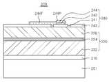
도 1은 본 발명의 일 실시형태에 의한 반도체 발광소자의 평면도이고, 도 2는 도 1의 반도체 발광소자를 I-I'축을 따라 절개한 측단면도이며, 도 3은 도 1의 반도체 발광소자를 II-II'축을 따라 절개한 측단면도이고, 도 4는 도 1의 제2 전극부를 부분절개한 사시도이다.
1 is a plan view of a semiconductor light emitting device according to an embodiment of the present invention, FIG. 2 is a side cross-sectional view of the semiconductor light emitting device of FIG. 1 taken along the line II ′, and FIG. 3 is a view of the semiconductor light emitting device of FIG. 1. FIG. 4 is a side cross-sectional view taken along the line II-II ′, and FIG. 4 is a perspective view partially cut away of the second electrode part of FIG. 1.
도 1 내지 도 3을 참조하면, 본 발명의 일 실시형태에 의한 반도체 발광소자(100)는 발광구조물(120) 및, 제1 및 제2 전극(130, 140)을 포함한다.
1 to 3, a semiconductor
상기 발광구조물(120)은 제1 및 제2 도전형 반도체층(122, 126) 및 활성층(124)을 포함한다. 상기 제1 및 제2 도전형 반도체층(122, 126)에 전원이 인가되면 상기 활성층(124)에서 빛이 방출된다.
The
구체적으로, 상기 발광구조물(120)은 질화물 반도체층일 수 있으며, 상기 제1 도전형 반도체층(122)은 n형 반도체층을, 상기 제2 도전형 반도체층(126)은 p형 반도체층을 포함할 수 있다.
Specifically, the
상기 n형 반도체층 및 p형 반도체층은 AlxInyGa(1-x-y)N 조성식을 갖는 n형 불순물 및 p형 불순물이 도핑된 반도체 물질로 형성될 수 있으며, 대표적으로, GaN, AlGaN, InGaN이 사용될 수 있다. 이때, 상기 x, y 값은 각각 0≤x≤1, 0≤y≤1, 0≤x+y≤1의 범위 내로 할 수 있다.
The n-type semiconductor layer and the p-type semiconductor layer may be formed of a semiconductor material doped with n-type impurities and p-type impurities having an Alx Iny Ga(1-xy) N composition formula, typically, GaN, AlGaN, InGaN can be used. In this case, the x and y values may be in the range of 0 ≦ x ≦ 1, 0 ≦ y ≦ 1, and 0 ≦ x + y ≦ 1, respectively.
또한, 상기 n형 불순물로 Si, Ge, Se, Te 또는 C 등이 사용될 수 있으며, 상기 p형 불순물로는 Mg, Zn 또는 Be 등이 대표적이다.
In addition, Si, Ge, Se, Te, or C may be used as the n-type impurity, and the p-type impurity may be representative of Mg, Zn or Be.
본 실시형태에서는 제1 및 제2 도전형 반도체층(122, 126)으로 GaN층을 사용할 수 있으며, 상기 제1 도전형 반도체층(122)으로 n-GaN을, 상기 제2 도전형 반도체층(126)으로 p-GaN을 사용할 수 있다.
In the present embodiment, a GaN layer may be used as the first and second
상기 발광 구조물(120)은 기판(101) 상에 유기금속 기상증착법(metal organic chemical vapor deposition ; MOCVD), 분자빔성장법(molecular beam epitaxy ; MBE) 및 수소 기상증착법(hydride vapor phase epitaxy ; HVPE)등으로 성장될 수 있다. 상기 기판(101)으로는 사파이어, 실리콘 카바이드(SiC), 실리콘(Si), MgAl2O4, MgO, LiAlO2, LiGaO2 또는 GaN 중의 어느 하나가 사용될 수 있으나, 이에 한정하는 것은 아니다. 본 실시형태에서는 사파이어 기판이 사용될 수 있다.
The
사파이어는 육각-롬보형(Hexa-Rhombo R3c) 대칭성을 갖는 결정체로서 c축 및 a축 방향의 격자상수가 각각 13.001Å과 4.758Å이며, C(0001)면, A(1120)면, R(1102)면 등을 갖는다. 이 경우, 상기 C면은 비교적 질화물 박막의 성장이 용이하며, 고온에서 안정하기 때문에 질화물 성장용 기판으로 주로 사용된다.
Sapphire is a Hexa-Rhombo R3c symmetric crystal, whose lattice constants in the c-axis and a-axis directions are 13.001Å and 4.758Å, respectively, C (0001) plane, A (1120) plane, and R (1102). ) And the like. In this case, the C plane is mainly used as a nitride growth substrate because the C surface is relatively easy to grow and stable at high temperatures.
또한, 상기 제1 도전형 반도체층(122)의 하부에는 버퍼(buffer)층(110)이 더 형성될 수 있다.
In addition, a
상기 버퍼층(110)은, 상기 기판(101) 상에 성장되는 발광구조물(120)의 격자 결함 완화를 위한 것으로, 질화물 등으로 이루어진 언도프 반도체층으로 이루어질 수 있다. 예를 들면, 기판(101)으로 이용되는 사파이어 기판과, 그 상면에 적층되는 GaN으로 이루어진 발광구조물(120)과의 격자상수 차이를 완화하여, GaN층의 결정성을 증대시킬 수 있다. 이때 버퍼층(110)은 언도프 GaN, AlN, InGaN 등이 적용될 수 있으며, 500 내지 600℃의 저온에서 수십 내지 수백 Å의 두께로 성장할 수 있다. 이 경우, 언도프라 함은 반도체층에 불순물 도핑 공정을 따로 거치지 않은 것을 의미하며, 반도체층에 본래 존재하던 수준의 불순물 농도, 예컨대, 질화갈륨 반도체를 MOCVD를 이용하여 성장시킬 경우, 도펀트로 사용되는 Si 등이 의도하지 않더라도 약 1014~ 1018/㎤인 수준으로 포함될 수 있다.
The
상기 활성층(124)은 가시광(약 350㎚∼680㎚ 파장범위)을 발광하기 위한 층일 수 있으며, 단일 또는 다중 양자 우물(multiple quantum well ; MQW )구조를 갖는 언도프된 질화물 반도체층으로 구성될 수 있다. 상기 활성층(124)은 양자우물층과 양자장벽층이 교대로 적층된 다중양자우물구조로 이루어지되, 예를 들어 AlxInyGa(1-x-y)N (0≤x≤1, 0≤y≤1, 0≤x+y≤1)의 양자장벽층과 양자우물층이 교대로 적층된 다중양자우물구조로 형성되어 소정의 밴드 갭을 가지며, 이와 같은 양자 우물에 의해 전자 및 정공이 재결합되어 발광한다.
The
상기 제1 및 제2 도전형 반도체층(122, 126)에는 각각 제1 및 제2 전극(130, 140)이 형성된다. 상기 제1 및 제2 전극(130, 140)은 각각 제1 및 제2 도전형 반도체층(122, 126)에 전기적으로 연결되어, 전원을 인가하면 상기 발광구조물(120)의 활성층(124)에서 빛이 방출되게 한다.
First and
또한, 상기 제1 및 제2 전극(130, 140)은 외부 전기 신호 인가를 위하여 도전성 와이어나 솔더 범프 등과 접촉하는 영역으로 제공된다. 상기 제1 전극(130)은 발광구조물(120)에서 활성층(124) 및 제2 도전형 반도체층(126)이 일부 제거되어 노출된 제1 도전형 반도체층(122)의 일부 상면에 형성될 수 있으며, 전류 확산이 더욱 효율적으로 이루어질 수 있도록 제1 도전형 반도체층(122)의 노출된 상면에서 발광구조물(120)의 외곽을 따라 배치될 수 있다.
In addition, the first and
상기 제1 전극(130)은 제1 반사부(134) 및 제1 전극부(136)를 포함한다. 상기 제1 반사부(134)는 활성층(124)에서 방출된 빛이 전극 영역에서 흡수되는 것을 방지하는 역할을 수행할 수 있으며, 제1 도전형 반도체층(122)과 오믹 특성을 갖는 도전성 물질의 단일층 또는 다층 구조로 이루어질 수 있다. 예컨대, 제1 반사부(134)는 Ag, Al, Rh 또는 Ir 중 어느 하나를 포함할 수 있으며, Mg, Zn, Sc, Hf, Zr, Te, Se, Ta, W, Nb, Cu, Si, Ni, Co, Mo, Cr, Mn, Hg, Pr 또는 La 중 적어도 하나와 Ag 또는 Al의 합금일 수 있다.
The
상기 제1 전극부(136)는 도전성 와이어나 솔더 범프 등과 접촉하는 영역일 수 있으며, Au, W, Pt, Si, Ir, Ag, Cu, Ni, Ti, Cr, Al 등의 물질 및 그 합금 중 하나 이상을 포함하되, 제1 반사부(134)와 상이한 물질을 포함할 수 있다.
The
상기 제2 전극(140)은 전류차단층(141), 상기 전류차단층(141) 상에 형성된 제2 반사부(142), 상기 제2 반사부(142)를 둘러싸는 개구부(OP)가 형성된 투명전극층(143) 및 상기 제2 반사부(142)를 덮는 제2 전극부(144)를 포함할 수 있다.
The
상기 전류차단층(141)은 제2 도전형 반도체층(126) 상면 중 일 영역에 배치될 수 있으며, 절연성 물질을 포함할 수 있다. 상기 절연성 물질로는 SiO2, SiN, Al2O3, HfO, TiO2 또는 ZrO 중 어느 하나를 포함할 수 있다. 상기 전류차단층(141)은 상기 제2 전극부(144)에서 인가된 전기적 신호가 발광구조물(120)의 상부로 곧바로 유입되어 상기 제2 전극부(144)의 하부에 집중되는 현상을 완화시켜 전류 확산(current spreading)이 효율적으로 이루어질 수 있다.
The
구체적으로, 상기 전류차단층(141)은 도 1에 도시된 바와 같이, 제2 도전형 반도체층(126)의 상면에서 보았을 때, D3의 지름을 가지는 원형으로, 상기 패드 전극부(144P)의 하부에만 형성할 수 있으나, 이에 한정하는 것은 아니며 상기 핑거 전극부(144F)의 하부에 상기 핑거 전극부(144F)를 따라서 연장 형성하는 것과 같이, 다양한 형상으로 변형할 수 있다.
Specifically, as illustrated in FIG. 1, the
상기 제2 반사부(142)는 상기 전류차단층(141) 상에 형성되되, 상기 제2 도전형 반도체층(126)과 접하지 않도록 상기 전류차단층(141)의 상부에만 형성될 수 있다. 구체적으로, 상기 제2 반사부(142)는 제2 도전형 반도체층(126)의 상면에서 보았을 때, D3보다 작은 지름을 가지는 원형으로 형성할 수 있으나, 반드시 이에 한정하는 것은 아니며, 상기 전류차단층(141) 상에 다양한 형상으로 변형할 수 있다.
The
상기 제2 반사부(142)는 제1 반사부(134)와 같이, 상기 활성층(124)에서 방출되는 광이 흡수되지 않도록, 광을 반사하여 상기 반도체 발광소자(100)의 외부 광추출 효율을 향상시킬 수 있다. 상기 제2 반사부(142)는 표면 반사율이 향상되도록, 그 표면이 매끈하게 가공될 수 있으며, 소정의 표면 반사율을 갖도록 표면에 요철을 형성할 수도 있다. 상기 제2 반사부(142)는 고반사형 금속인 Ag, Al, Rh 또는 Ir 중 어느 하나를 포함할 수 있으며, Mg, Zn, Sc, Hf, Zr, Te, Se, Ta, W, Nb, Cu, Si, Ni, Co, Mo, Cr, Mn, Hg, Pr 또는 La 중 적어도 하나와 Ag 또는 Al의 합금일 수 있다. 또한, 상기 제2 반사부(142)의 상부에는 Ti을 증착하여 상기 제2 반사부(142)의 산화를 방지할 수도 있다.
Like the
상기 제2 반사부(142)는 상기 투명전극층(143)의 개구부(OP) 내에 형성되되, 상기 개구부(OP)의 측면과 소정의 간격을 두고 형성될 수 있다. 상기 제2 반사부(142)와 상기 투명전극층(143)이 접하게 되면, 상기 투명전극층(143)이 변색되어 상기 활성층(124)에서 방출되는 광의 외부 광추출효율이 저하될 수 있다. 따라서, 상기 제2 반사부(142)는 상기 투명전극층(143)와 접하지 않도록 상기 개구부(OP)의 측면과 간격을 두고 형성하면 상기 투명전극층(143)의 변색을 방지하여, 상기 반도체 발광소자(100)의 외부 광추출 효율을 향상시킬 수 있다.
The
상기 투명전극층(143)은 전류확산층으로서, 상기 제2 도전형 반도체층(126)의 상면에 형성된다. 상기 투명전극층(143)은 투명 전도성 산화물층으로 형성할 수 있으며, ITO(Indium Tin Oxide), ZITO(Zinc-doped Indium Tin Oxide), ZIO(Zinc Indium Oxide), GIO(Gallium Indium Oxide), ZTO(Zinc TinOxide), FTO(Fluorine-doped Tin Oxide), AZO(Aluminium-doped Zinc Oxide), GZO(Gallium-doped Zinc Oxide), In4Sn3O12 및 Zn(1-x)MgxO(Zinc Magnesium Oxide, 0≤x≤1)으로 구성된 그룹으로부터 선택될 수 있다.
The
상기 투명전극층(143)의 적어도 일 영역에는 개구부(OP)가 형성되며, 상기 개구부(OP)의 바닥면에는 상기 전류차단층(141)의 상면이 노출되도록 형성될 수 있다. 이때, 상기 투명전극층(143)의 적어도 일부 영역은 상기 전류차단층(141)과 접하도록 형성된다. 구체적으로, 도 1에 도시된 바와 같이, 상기 개구부(OP)는 상기 전류차단층(141)의 지름(D3)보다 작은 지름(D2)을 갖는 원형으로 보이도록 형성할 수 있으나, 이에 한정하는 것은 아니며, 다양한 형상으로 변형할 수도 있다.
An opening OP may be formed in at least one region of the
상기 제2 전극부(144)는 상기 제2 반사부(142)를 덮으며, 상기 투명전극층(143)과 접하지 않도록 소정 간격 이격되어 형성될 수 있다. 상기 제2 전극부(144)는 Au, W, Pt, Si, Ir, Ag, Cu, Ni, Ti, Cr, Al로 구성된 그룹으로부터 선택된 적어도 하나로 형성될 수 있으며, 다층 구조를 이룰 수도 있다. 상기 제2 전극부(144)는 패드 전극부(144P)와 핑거 전극부(144F)로 구성될 수 있다. 상기 패드 전극부(144P)는 상기 제2 반사부(142)를 덮으며 상기 투명전극층(143)과 이격되도록 형성된 영역이다. 상기 핑거 전극부(144F)는 상기 패드 전극부(144P)의 일 측면으로부터 일 방향으로 연장되어 형성되며 적어도 일부는 상기 투명전극층(143) 상에 형성될 수 있다. 상기 핑거 전극부(144F)는 상기 패드 전극부(144P)에 비해 좁고 길게 형성되어, 상기 제2 전극부(144)에 인가되는 전기적 신호가 상기 패드 전극부(144P)의 하부에 집중되는 현상을 완화시키므로, 전류 확산(current spreading)이 효율적으로 이루어질 수 있다.
The
이와 같은 구성의 상기 반도체 발광소자(100)는 상기 패드 전극부(144P)가 전류차단층(141) 상에 형성되며, 상기 패드 전극부(144P)와 투명전극층(143)은 서로 이격되어 배치되므로, 상기 패드 전극부(144P)는 상기 제2 도전형 반도체층(126)과 전기적으로 절연상태가 되게 된다. 따라서, 상기 패드 전극부(144P)를 통하여 상기 제2 도전형 반도체층(126)에 직접 인가되는 전기적 신호가 차단되므로 상기 패드 전극부(144P)의 하부 영역에만 전기적 신호가 인가되는 현상이 근본적으로 방지된다. 또한, 패드 전극부(144P)에 인가된 전기적 신호는 핑거 전극부(144F)를 통해 투명전극층(143)에 인가되어 상기 제2 도전형 반도체층(126)의 상부에 넓게 확산되므로, 종래의 발광소자에 비해 전류 확산이 더욱 효율적으로 이루어질 수 있다.
In the semiconductor
도 9를 참조하여 본 발명의 일 실시형태에 의한 반도체 발광소자의 효과를 설명한다. 도 9는 패드전극부와 투명전극층이 이격 형성된 반도체 발광소자의 휘도값(904, 905, 906)과 패드전극부와 투명전극층이 접하도록 형성된 반도체 발광소자의 휘도값(901, 902, 903)을 비교한 그래프이다. 901과 904, 902와 905, 903과 906은 각각 패드 전극부와 투명전극층의 구성만 차이가 나는 반도체 발광소자의 휘도값으로서, 각각 동일한 제조공정을 통하여 제조된 반도체 발광소자이다.
9, the effect of the semiconductor light emitting element according to the embodiment of the present invention will be described. 9 illustrates
이를 참조하면, 패드전극부와 투명전극층이 이격 형성되어 핑거 전극부만을 통하여 전기적 신호가 인가된 경우에 패드 전극부를 통해 전기적 신호가 인가된 경우에 비해서 각각 약 0.6%, 1.2%, 1.5%의 휘도가 향상되었음을 확인할 수 있다.
Referring to this, when the pad electrode portion and the transparent electrode layer are formed apart from each other and an electric signal is applied through only the finger electrode portion, the luminance is about 0.6%, 1.2% and 1.5%, respectively, compared to the case where the electric signal is applied through the pad electrode portion. It can be seen that is improved.
다음으로, 도 8을 참조하여, 도 1의 반도체 발광소자의 변형예에 대해 설명한다. 상기 변형예의 경우, 앞서 설명한 일 실시형태와 비교하여, 패드 전극부(344P)와 상기 투명전극층(343)을 전기적으로 연결하는 연결부(345)를 더 포함한 차이점이 있다. 이 외의 구성은 앞서 설명한 일 실시형태와 같으므로, 일 실시형태와 다른 구성을 중심으로 설명한다.
Next, with reference to FIG. 8, the modification of the semiconductor light emitting element of FIG. 1 is demonstrated. In the case of the modified example, there is a difference that further includes a connecting
상기 연결부(345)는 소정 길이로 절단된 형태로 형성되되, 핑거 전극부(344F)와 같이 좁고 긴 형상을 가지며, 핑거 전극부(344F)보다 짧은 길이로 형성될 수 있다. 상기 연결부(345)의 일단은 상기 투명전극층(343) 상에 배치되며 타단은 상기 패드 전극부(344P) 상에 배치되어, 상기 패드 전극부(344P)와 상기 투명전극층(343)을 전기적으로 연결하도록 형성된다.
The
상기 연결부(345)는 상기 패드 전극부(344P)의 주위에 형성된 투명전극층(343)의 개구부(OP) 주위에 전기적 신호를 공급하여 전류 확산을 더욱 향상시키기 위한 구성으로, 앞서 설명한 일 실시형태에 상기 연결부(345)를 더 형성하면, 전류 확산이 더욱 효율적으로 이루어질 수 있다.
The
상기 연결부(345)는 인접한 핑거 전극부(344F)와 이격된 간격이 최대가 되는 영역에 배치하여, 상기 핑거 전극부(344F)가 배치되지 않은 영역의 전류 확산을 더욱 향상시킬 수 있다. 또한, 상기 연결부(345)는 복수개가 형성될 수 있으며, 복수개로 형성할 경우에는 상기 패드 전극부(344P)의 주변에 방사형으로 배치할 수 있다.상기 연결부(345)를 복수개로 형성할 경우에는 인접한 핑거 전극부(344F) 또는 인접한 연결부(345)와 이격된 간격이 최대의 되는 영역에 형성하여, 전류 확산 효과를 높일 수 있다. 이때, 상기 복수개의 연결부(345)는 인접한 상기 핑거 전극부(344F) 또는 인접한 연결부(344)와 서로 동일 간격으로 이격되도록 형성할 수 있다.
The
이를 구체적을 설명하면, 하나의 핑거 전극부(344F)와 하나의 연결부(345)가 형성된 경우에, 상기 연결부(345)는 상기 핑거 전극부(344F)와 이루는 각도가 180도를 이루도록, 상기 핑거 전극부(344F)가 형성된 영역의 반대영역에 배치할 수 있다. 또한, 하나의 핑거 전극부(344F)와 두개의 연결부(345)가 형성된 경우에는, 도 8에 도시된 바와 같이, 상기 핑거 전극부(344F)와 두개의 연결부(345)가 각각 120도의 각도를 이루도록 배치할 수 있다.
In detail, when one
상기 연결부(345)는 전극부(344)와 같이 Au, W, Pt, Si, Ir, Ag, Cu, Ni, Ti, Cr, Al로 구성된 그룹으로부터 선택된 적어도 하나로 형성될 수 있으며, 다층 구조를 이룰 수도 있다.
The
다음으로, 도 9를 참조하여 도 1의 반도체 발광소자의 다른 변형예를 설명하고, 도 10을 참조하여 개선된 효과를 설명한다.
Next, another modified example of the semiconductor light emitting device of FIG. 1 will be described with reference to FIG. 9, and the improved effect will be described with reference to FIG. 10.
상기 다른 변형예의 경우, 앞서 설명한 일 실시형태와 비교하여, 제2 전극부(444)의 핑거 전극부(444F)가 패드 전극부(444P)의 복수개의 영역에 연장 형성된 차이점이 있다. 다만, 핑거 전극부(444F)의 개수는 도면에 도시된 것에 한정하지 않으며, 실시형태에 따라 다양하게 변화될 수 있다. 전류차단층(441), 상기 전류차단층(441) 상에 형성된 반사부(442), 상기 반사부(442)를 둘러싸는 개구부(OP)가 형성된 투명전극층(443)의 구성은 앞서 설명한 일 실시형태와 같으므로, 일 실시형태와 다른 구성을 중심으로 설명한다.
In the case of the other modified example, there is a difference in that the
상기 복수개의 핑거 연결부(444F)는 좁고 긴 형상을 가지되, 반도체 발광소자(300)의 길이 방향을 따라 서로 평행하게 형성될 수 있다. 또한, 상기 핑거 연결부(344P)의 사이에 제1 전극(430)이 교대로 엇갈리도록 배치할 수도 있다.
The plurality of
도 9 및 도 10을 참조하여, 상기 다른 변형예와 비교예의 효과를 비교한다. 도 10은 상기 다른 변형예와 비교예의 광량을 비교한 그래프이다. 상기 비교예는 상기 다른 변형예의 패드 전극부(444P)와 투명전극층(443)을 서로 접하도록 배치한 차이점이 있으며, 이 외의 구성은 상기 다른 변형예와 같다.
With reference to FIG. 9 and FIG. 10, the effect of the said other modified example and a comparative example is compared. 10 is a graph comparing the amounts of light of the other modified examples and the comparative example. The comparative example has a difference in which the
도 11(a)는 도 9의 반도체 발광소자(400)의 L1-L1’축을 따라 광량을 측정한 그래프이며, 도 11(b)는 도 9의 반도체 발광소자(400)의 L2-L2’축을 따라 광량을 측정한 그래프이며, 도 11(c)는 도 9의 반도체 발광소자(400)의 L3-L3’축을 따라 광량을 측정한 그래프이다. 각 그래프의 A, B, C 영역을 보면, 본 발명이 비교예에 비하여 거의 모든 영역에서 전반적으로 광량이 증가함을 알 수 있다. 이와 같은 결과로부터, 상기 패드 전극부(444P)와 상기 투명전극층(443)을 서로 이격 배치한 경우에 전류 확산이 더욱 효율적으로 이루어 짐을 확인할 수 있다.
FIG. 11A is a graph measuring light quantity along the L1-L1 'axis of the semiconductor
다음으로, 도 5 내지 도 7을 참조하여 본 발명의 다른 실시형태의 반도체 발광소자(200)를 설명한다. 도 5는 본 발명의 다른 실시형태에 의한 반도체 발광소자의 평면도이고, 도 6은 도 5의 반도체 발광소자를 III-III'축을 따라 절개한 측단면도이며, 도 7은 도 5의 반도체 발광소자를 IV-IV'축을 따라 절개한 측단면도이다.
Next, the semiconductor
본 실시형태의 경우, 앞서 설명한 일 실시형태와 비교하여, 전류차단층(241)이 투명전극층(243)과 이격되어 배치된 차이점이 있다. 그 외의 구성은 일 실시형태와 같으므로, 일 실시형태와 다른 구성을 중심으로 설명한다.
In the case of the present embodiment, there is a difference in that the
도 5 및 도 6에 도시된 바와 같이, 본 발명의 다른 실시형태에 의한 반도체 발광소자(200)는, 앞서 설명한 일 실시형태와 동일하게 제1 및 제2 도전형 반도체층(222, 226), 활성층(224), 제1 전극(230) 및 제2 전극(240)을 포함한다.
As shown in FIGS. 5 and 6, the semiconductor
상기 제2 전극(240)은 전류차단층(241), 상기 전류차단층(241) 상에 형성된 반사부(242), 상기 반사부(242)를 둘러싸는 개구부(OP)가 형성된 투명전극층(243) 및 상기 반사부(242)를 덮는 제2 전극부(144)를 포함할 수 있다.
The
앞서 설명한 바와 같이, 제2 도전형 반도체층(226)의 일 영역에는 전류차단층(241)이 형성된다.
As described above, the
상기 투명전극층(243)은 적어도 일 영역에는 개구부(OP)가 형성되되, 상기 개구부(OP)의 측면은 상기 전류차단층(241)과 이격되도록 형성되어, 상기 투명전극층(243)과 상기 전류차단층(241)이 서로 접하지 않도록 배치된다.
An opening OP is formed in at least one region of the
앞서 설명한 일 실시형태와 같이, 상기 전류차단층(241)의 상부에는 반사부(242)가 형성되며, 상기 반사부(242)를 덮으며 상기 투명전극층(243)과 이격되도록 패드 전극부(244P)를 형성한다.
As described above, the
따라서, 본 실시형태는 앞서 설명한 일 실시형태와 비교하여, 전류차단층(241)이 투명전극층(243)과 이격되어 배치되게 된다.
Therefore, in the present embodiment, the
이와 같이, 전류차단층(241)과 투명전극층(243)를 이격하면, 상기 전류차단층(241) 상에 형성되는 반사부(242)와 상기 투명전극층(243)의 절연성이 더욱 향상되는 장점이 있다.
As such, when the
또한, 전류차단층(241)과 투명전극층(243)이 중첩되는 영역을 형성할 필요가 없으므로, 일 실시형태에 비해 투명전극측(244)의 개구(OP)를 더 넓게 형성할 수 있게 되어, 상기 개구(OP) 내에 배치되는 반사부(242)를 좀 더 넓게 형성할 수 있는 효과가 있다. 아울러, 반사부(242)의 면적이 넓어지게 되면 반도체 발광소자(200)의 반사율이 증가하게 되어 외부 광추출 효율이 더욱 향상되는 효과를 기대할 수 있다.
In addition, since it is not necessary to form a region where the
또한, 앞서 설명한 바와 같이, 상기 반사부(242)는 상기 투명전극층(244)에 접하여 형성될 경우, 상기 투명전극층(244)이 변색되어 광투광율이 저하되는 문제점이 발생하므로, 상기 반사부(242)는 상기 투명전극층(244)과 닿지 않도록 간격을 두고 형성된다. 본 실시형태에 의한 반도체 발광소자(200)은, 도 7에 도시된 바와 같이, 상기 투명전극층(243)이 상기 전류차단층(241)과 접하는 영역이 형성되지 않게 되므로, 반사부(242)가 투명전극층(243)과 접하여 변색될 가능성이 더욱 낮아지게 되어 반도체 발광소자(200)의 신뢰성이 더욱 향상되는 효과를 기대할 수 있다.
In addition, as described above, when the
도 12 및 도 13은 본 발명의 일 실시형태에 따른 반도체 발광소자를 패키지에 적용한 예를 나타낸다.12 and 13 show an example in which a semiconductor light emitting device according to an embodiment of the present invention is applied to a package.
도 12를 참조하면, 반도체 발광소자 패키지(1000)는 반도체 발광소자(1001), 패키지 본체(1002) 및 한 쌍의 리드 프레임(1003)을 포함하며, 반도체 발광소자(1001)는 리드 프레임(1003)에 실장되어 와이어(W)를 통하여 리드 프레임(1003)과 전기적으로 연결될 수 있다. 실시형태에 따라, 반도체 발광소자(1001)는 리드 프레임(1003) 아닌 다른 영역, 예컨대, 패키지 본체(1002)에 실장될 수도 있을 것이다. 또한, 패키지 본체(1002)는 빛의 반사 효율이 향상되도록 컵 형상을 가질 수 있으며, 이러한 반사컵에는 반도체 발광소자(1001)와 와이어(W) 등을 봉지하도록 투광성 물질로 이루어진 봉지체(1005)가 형성될 수 있다. 본 실시형태에서, 반도체 발광소자 패키지(1000)는 도 1 내지 도 8중 어느 하나의 반도체 발광소자를 포함할 수 있다.
12, the semiconductor light emitting
도 13을 참조하면, 반도체 발광소자 패키지(2000)는 반도체 발광소자(2001), 실장 기판(2010) 및 봉지체(2003)를 포함한다. 또한, 반도체 발광소자(2001)의 표면 및 측면에는 파장변환부(2002)가 형성될 수 있다. 반도체 발광소자(2001)는 실장 기판(2010)에 실장되어 와이어(W)를 통하여 실장 기판(2010)과 전기적으로 연결될 수 있다.Referring to FIG. 13, the semiconductor light emitting
실장 기판(2010)은 기판 본체(2011), 상면 전극(2013) 및 하면 전극(2014)을 구비할 수 있다. 또한, 실장 기판(2010)은 상면 전극(2013)과 하면 전극(2014)을 연결하는 관통 전극(2012)을 포함할 수 있다. 실장 기판(2010)은 PCB, MCPCB, MPCB, FPCB 등의 기판으로 제공될 수 있으며, 실장 기판(2010)의 구조는 다양한 형태로 응용될 수 있다.The mounting
파장변환부(2002)는 형광체나 양자점 등을 포함할 수 있다. 봉지체(2003)는 상면이 볼록한 돔 형상의 렌즈 구조로 형성될 수 있지만, 실시형태에 따라, 표면을 볼록 또는 오목한 형상의 렌즈 구조로 형성함으로써 봉지체(2003) 상면을 통해 방출되는 빛의 지향각을 조절하는 것이 가능하다.The
본 실시형태에서, 반도체 발광소자 패키지(2000)는 도 1 내지 도 8 중 어느 하나의 반도체 발광소자를 포함할 수 있다.
In the present embodiment, the semiconductor light emitting
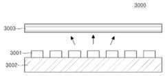
도 14 및 도 15는 본 발명의 일 실시형태에 따른 반도체 발광소자를 백라이트 유닛에 적용한 예를 나타낸다.14 and 15 show an example in which a semiconductor light emitting device according to an embodiment of the present invention is applied to a backlight unit.
도 14를 참조하면, 백라이트 유닛(3000)은 기판(3002) 상에 광원(3001)이 실장되며, 그 상부에 배치된 하나 이상의 광학 시트(3003)를 구비한다. 광원(3001)은 도 12 및 도 13을 참조하여 상술한 구조 또는 그와 유사한 구조를 갖는 반도체 발광소자 패키지를 이용할 수 있으며, 또한, 도 1 내지 도 8 중 어느 하나의 반도체 발광소자를 직접 기판(3002)에 실장(소위 COB 타입)하여 이용할 수도 있다.Referring to FIG. 14, the
도 14의 백라이트 유닛(3000)에서 광원(3001)은 액정표시장치가 배치된 상부를 향하여 빛을 방사하는 것과 달리, 도 15에 도시된 다른 예의 백라이트 유닛(4000)은 기판(4002) 위에 실장된 광원(4001)이 측 방향으로 빛을 방사하며, 이렇게 방시된 빛은 도광판(4003)에 입사되어 면광원의 형태로 전환될 수 있다. 도광판(4003)을 거친 빛은 상부로 방출되며, 광 추출 효율을 향상시키기 위하여 도광판(4003)의 하면에는 반사층(4004)이 배치될 수 있다.
In the
도 16은 본 발명의 실시예에 의한 반도체 발광소자를 조명 장치에 적용한 예를 나타낸다.16 shows an example in which the semiconductor light emitting device according to the embodiment of the present invention is applied to a lighting device.
도 16의 분해사시도를 참조하면, 분해사시도를 참조하면, 조명장치(5000)는 일 예로서 벌브형 램프로 도시되어 있으며, 발광모듈(5003)과 구동부(5008)와 외부접속부(5010)를 포함한다. 또한, 외부 및 내부 하우징(5006, 5009)과 커버부(5007)와 같은 외형구조물을 추가적으로 포함할 수 있다. 발광모듈(5003)은 도 12 및 도 13을 참조하여 상술한 반도체 발광소자 패키지 구조 또는 이와 유사한 구조를 갖는 광원(5001)과 그 광원(5001)이 탑재된 회로기판(5002)을 포함할 수 있다. 본 실시형태에서는, 하나의 광원(5001)이 회로기판(5002) 상에 실장된 형태로 예시되어 있으나, 필요에 따라 복수 개로 장착될 수 있다.Referring to the exploded perspective view of FIG. 16, referring to the exploded perspective view, the
외부 하우징(5006)은 열방출부로 작용할 수 있으며, 발광모듈(5003)과 직접 접촉되어 방열효과를 향상시키는 열방출판(5004) 및 조명장치(5000)의 측면을 둘러싸는 방열핀(5005)을 포함할 수 있다. 커버부(5007)는 발광모듈(5003) 상에 장착되며 볼록한 렌즈형상을 가질 수 있다. 구동부(5008)는 내부 하우징(5009)에 장착되어 소켓구조와 같은 외부접속부(5010)에 연결되어 외부 전원으로부터 전원을 제공받을 수 있다. 또한, 구동부(5008)는 발광모듈(5003)의 광원(5001)을 구동시킬 수 있는 적정한 전류원으로 변환시켜 제공하는 역할을 한다. 예를 들어, 이러한 구동부(5008)는 AC-DC 컨버터 또는 정류회로부품 등으로 구성될 수 있다.The
또한, 도면에는 도시되지 않았으나, 조명장치(5000)는 통신 모듈을 더 포함 할 수도 있다.
In addition, although not shown in the drawings, the
도 17은 본 발명의 실시예에 의한 반도체 발광소자를 헤드 램프에 적용한 예를 나타낸다.17 shows an example in which the semiconductor light emitting device according to the embodiment of the present invention is applied to a head lamp.
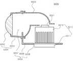
도 17을 참조하면, 차량용 라이트 등으로 이용되는 헤드 램프(6000)는 광원(6001), 반사부(6005), 렌즈 커버부(6004)를 포함하며, 렌즈 커버부(6004)는 중공형의 가이드(6003) 및 렌즈(6002)를 포함할 수 있다. 광원(6001)은 도 12 및 도 13의 반도체 발광소자 패키지를 적어도 하나 포함할 수 있다.Referring to FIG. 17, a
헤드 램드(6000)는 광원(6001)에서 발생된 열을 외부로 방출하는 방열부(6012)를 더 포함할 수 있으며, 방열부(6012)는 효과적인 방열이 수행되도록 히트싱크(6010)와 냉각팬(6011)을 포함할 수 있다. 또한, 헤드 램프(6000)는 방열부(6012) 및 반사부(6005)를 고정시켜 지지하는 하우징(6009)을 더 포함할 수 있으며, 하우징(6009)은 일면에 방열부(6012)가 결합하여 장착되기 위한 중앙홀(6008)을 구비할 수 있다.The
하우징(6009)은 상기 일면과 일체로 연결되어 직각방향으로 절곡되는 타면에 반사부(6005)가 광원(6001)의 상부측에 위치하도록 고정시키는 전방홀(6007)을 구비할 수 있다. 이에 따라, 반사부(6005)에 의하여 전방측은 개방되며, 개방된 전방이 전방홀(6007)과 대응되도록 반사부(6005)가 하우징(6009)에 고정되어 반사부(6005)를 통해 반사된 빛이 전방홀(6007)을 통과하여 외부로 출사될 수 있다.
The
본 발명은 상술한 실시형태 및 첨부된 도면에 의해 한정되는 것이 아니며 첨부된 청구범위에 의해 한정하고자 한다. 따라서, 청구범위에 기재된 본 발명의 기술적 사상을 벗어나지 않는 범위 내에서 당 기술분야의 통상의 지식을 가진 자에 의해 다양한 형태의 치환, 변형 및 변경이 가능할 것이며, 이 또한 본 발명의 범위에 속한다고 할 것이다.
It is intended that the invention not be limited by the foregoing embodiments and the accompanying drawings, but rather by the claims appended hereto. Accordingly, various forms of substitution, modification, and alteration may be made by those skilled in the art without departing from the technical spirit of the present invention described in the claims, which are also within the scope of the present invention. something to do.
100, 200, 300: 반도체 발광소자
101, 201, 301: 기판
110, 210, 310: 버퍼층
120, 220, 320: 발광구조물
122, 222, 322: 제1 도전형 반도체층
124, 224, 324: 활성층
126, 226, 326: 제2 도전형 반도체층
130, 230, 330: 제1 전극
140, 240, 340: 제2 전극
141, 241, 341: 전류차단층
142, 242, 342: 반사부
143, 243, 343: 투명전극층
144, 244, 344: 전극부
144F, 244F, 344F: 핑거 전극부
144P, 244P, 344P: 패드 전극부
345: 연결부100, 200, 300: semiconductor light emitting device
101, 201, 301: substrate
110, 210, 310: buffer layer
120, 220, 320: light emitting structure
122, 222, and 322: first conductive semiconductor layer
124, 224, 324: active layer
126, 226, 326: second conductive semiconductor layer
130, 230, and 330: first electrode
140, 240, and 340: second electrode
141, 241, 341: current blocking layer
142, 242, 342: reflector
143, 243, and 343: transparent electrode layer
144, 244, 344: electrode portion
144F, 244F, and 344F: finger electrode parts
144P, 244P, 344P: Pad electrode part
345: connection
Claims (10)
Translated fromKorean상기 제1 및 제2 도전형 반도체층과 각각 전기적으로 연결된 제1 및 제2 전극;을 포함하며,
상기 제2 전극은,
상기 제2 도전형 반도체층의 상면 중 일 영역에 형성된 전류차단층;
상기 전류 차단층 상에 형성된 반사부;
상기 반사부와 이격되어 배치되고, 상기 반사부를 둘러싸는 개구부를 가지며 상기 제2 도전형 반도체층 상에 형성되는 투명전극층;
상기 반사부를 덮으며 상기 투명전극층과 이격되어 형성되고 상기 전류차단층의 영역 내에 형성된 패드 전극부;
상기 패드 전극부로부터 일 방향으로 연장되어 형성되며 적어도 일부는 상기 투명전극층 상에 형성되는 적어도 하나의 핑거 전극부; 및
상기 패드 전극부와 상기 투명전극층을 전기적으로 연결하는 연결부;를 포함하며,
상기 패드 전극부는 상기 개구부의 측면과 일정간격 이격되며 상기 개구부의 영역 내에 배치된 것을 특징으로 하는 반도체 발광소자.
A light emitting structure in which a first conductive semiconductor layer, an active layer, and a second conductive semiconductor layer are sequentially stacked; And
And first and second electrodes electrically connected to the first and second conductive semiconductor layers, respectively.
The second electrode,
A current blocking layer formed on one region of an upper surface of the second conductive semiconductor layer;
A reflector formed on the current blocking layer;
A transparent electrode layer disposed to be spaced apart from the reflecting portion and having an opening surrounding the reflecting portion and formed on the second conductive semiconductor layer;
A pad electrode portion covering the reflecting portion and spaced apart from the transparent electrode layer and formed in an area of the current blocking layer;
At least one finger electrode portion extending from the pad electrode portion in one direction and at least partially formed on the transparent electrode layer; And
And a connection part electrically connecting the pad electrode part and the transparent electrode layer.
And the pad electrode portion is spaced apart from the side surface of the opening at a predetermined interval and disposed in an area of the opening.
상기 투명전극층은 적어도 일부 영역이 상기 전류차단층과 접하는 것을 특징으로 하는 반도체 발광소자.
The method of claim 1,
And at least a portion of the transparent electrode layer is in contact with the current blocking layer.
상기 연결부는 소정 길이로 절단된 형태로 형성되되, 상기 연결부의 일단은 상기 투명전극층 상에 배치되며 타단은 상기 패드 전극부 상에 배치되는 것을 특징을 하는 반도체 발광소자.
The method of claim 1,
The connecting portion is formed in a shape cut into a predetermined length, one end of the connecting portion is disposed on the transparent electrode layer, the other end is a semiconductor light emitting device, characterized in that disposed on the pad electrode portion.
상기 연결부는 인접한 상기 핑거 전극부와 이격된 간격이 최대가 되는 영역에 배치된 것을 특징으로 하는 반도체 발광소자.
The method of claim 1,
And the connection part is disposed in a region where a maximum distance from the adjacent finger electrode part is maximized.
상기 연결부는 복수개가 형성된 것을 특징으로 하는 반도체 발광소자.
The method of claim 1,
A plurality of the connection portion is a semiconductor light emitting device, characterized in that formed.
상기 복수개의 연결부는 인접한 상기 핑거 전극부과 서로 동일 간격으로 이격된 것을 특징으로 하는 반도체 발광소자.
The method of claim 7, wherein
The plurality of connection parts of the semiconductor light emitting device, characterized in that spaced apart from each other at equal intervals with the finger electrode portion.
상기 연결부는 상기 핑거 전극부보다 짧은 길이로 형성된 것을 특징으로 하는 반도체 발광소자.
The method of claim 1,
And the connection part is formed to have a length shorter than that of the finger electrode part.
상기 제1 및 제2 도전형 반도체층과 각각 전기적으로 연결된 제1 및 제2 전극;을 포함하며,
상기 제2 전극은,
상기 제2 도전형 반도체층의 상면 중 일 영역에 형성된 전류차단층;
상기 전류 차단층 상에 형성된 반사부;
상기 전류차단층과 이격되어 배치되고, 상기 전류차단층을 둘러싸는 개구부를 가지며 상기 제2 도전형 반도체층 상에 형성되는 투명전극층;
상기 반사부를 덮으며 상기 투명전극층과 이격되어 형성되고 상기 전류차단층의 영역 내에 형성된 패드 전극부; 및
상기 패드 전극부로부터 일 방향으로 연장되어 형성되며 적어도 일부는 상기 투명전극층 상에 형성되는 적어도 하나의 핑거 전극부;
를 포함하는 것을 특징으로 하는 반도체 발광소자.A light emitting structure in which a first conductive semiconductor layer, an active layer, and a second conductive semiconductor layer are sequentially stacked; And
And first and second electrodes electrically connected to the first and second conductive semiconductor layers, respectively.
The second electrode,
A current blocking layer formed on one region of an upper surface of the second conductive semiconductor layer;
A reflector formed on the current blocking layer;
A transparent electrode layer disposed to be spaced apart from the current blocking layer and having an opening surrounding the current blocking layer and formed on the second conductive semiconductor layer;
A pad electrode portion covering the reflecting portion and spaced apart from the transparent electrode layer and formed in an area of the current blocking layer; And
At least one finger electrode portion extending from the pad electrode portion in one direction and at least partially formed on the transparent electrode layer;
Semiconductor light emitting device comprising a.
Priority Applications (2)
| Application Number | Priority Date | Filing Date | Title |
|---|---|---|---|
| KR1020130123797AKR102075992B1 (en) | 2013-10-17 | 2013-10-17 | Semiconductor Light Emitting Device |
| US14/454,612US9548422B2 (en) | 2013-10-17 | 2014-08-07 | Semiconductor light emitting device including a pad electrode spaced apart from a transparent electrode |
Applications Claiming Priority (1)
| Application Number | Priority Date | Filing Date | Title |
|---|---|---|---|
| KR1020130123797AKR102075992B1 (en) | 2013-10-17 | 2013-10-17 | Semiconductor Light Emitting Device |
Publications (2)
| Publication Number | Publication Date |
|---|---|
| KR20150044583A KR20150044583A (en) | 2015-04-27 |
| KR102075992B1true KR102075992B1 (en) | 2020-02-11 |
Family
ID=52825422
Family Applications (1)
| Application Number | Title | Priority Date | Filing Date |
|---|---|---|---|
| KR1020130123797AActiveKR102075992B1 (en) | 2013-10-17 | 2013-10-17 | Semiconductor Light Emitting Device |
Country Status (2)
| Country | Link |
|---|---|
| US (1) | US9548422B2 (en) |
| KR (1) | KR102075992B1 (en) |
Families Citing this family (5)
| Publication number | Priority date | Publication date | Assignee | Title |
|---|---|---|---|---|
| KR20160086559A (en)* | 2015-01-12 | 2016-07-20 | 엘지이노텍 주식회사 | Light emitting device, light emitting device package having the same, and light system having the same |
| US9705035B1 (en)* | 2015-12-30 | 2017-07-11 | Epistar Corporation | Light emitting device |
| KR102707425B1 (en)* | 2017-01-06 | 2024-09-20 | 서울바이오시스 주식회사 | Light emitting device having currnt blocking layer |
| US10475962B2 (en)* | 2017-02-15 | 2019-11-12 | Epistar Corporation | Optoelectronic device |
| TWI702413B (en)* | 2019-03-21 | 2020-08-21 | 元太科技工業股份有限公司 | Proximity sensor and operation method thereof |
Family Cites Families (47)
| Publication number | Priority date | Publication date | Assignee | Title |
|---|---|---|---|---|
| CN1143394C (en) | 1996-08-27 | 2004-03-24 | 精工爱普生株式会社 | Peeling method, thin film device transfer method and thin film device |
| USRE38466E1 (en) | 1996-11-12 | 2004-03-16 | Seiko Epson Corporation | Manufacturing method of active matrix substrate, active matrix substrate and liquid crystal display device |
| US7208725B2 (en) | 1998-11-25 | 2007-04-24 | Rohm And Haas Electronic Materials Llc | Optoelectronic component with encapsulant |
| JP3906654B2 (en) | 2000-07-18 | 2007-04-18 | ソニー株式会社 | Semiconductor light emitting device and semiconductor light emitting device |
| US6818465B2 (en) | 2001-08-22 | 2004-11-16 | Sony Corporation | Nitride semiconductor element and production method for nitride semiconductor element |
| JP2003218034A (en) | 2002-01-17 | 2003-07-31 | Sony Corp | Selective growth method, semiconductor light emitting device and method of manufacturing the same |
| JP3815335B2 (en) | 2002-01-18 | 2006-08-30 | ソニー株式会社 | Semiconductor light emitting device and manufacturing method thereof |
| KR100489037B1 (en) | 2002-07-23 | 2005-05-11 | 엘지이노텍 주식회사 | Light emitting diode and fabrication method for thereof |
| KR100499129B1 (en) | 2002-09-02 | 2005-07-04 | 삼성전기주식회사 | Light emitting laser diode and fabricatin method thereof |
| US7002182B2 (en) | 2002-09-06 | 2006-02-21 | Sony Corporation | Semiconductor light emitting device integral type semiconductor light emitting unit image display unit and illuminating unit |
| KR100714639B1 (en) | 2003-10-21 | 2007-05-07 | 삼성전기주식회사 | Light emitting element |
| KR100506740B1 (en) | 2003-12-23 | 2005-08-08 | 삼성전기주식회사 | Nitride semiconductor light emitting device and method of manufacturing the same |
| KR100664985B1 (en) | 2004-10-26 | 2007-01-09 | 삼성전기주식회사 | Nitride-based semiconductor device |
| KR100665222B1 (en) | 2005-07-26 | 2007-01-09 | 삼성전기주식회사 | LED package using diffusion material and manufacturing method thereof |
| KR100661614B1 (en) | 2005-10-07 | 2006-12-26 | 삼성전기주식회사 | Nitride-based semiconductor light emitting device and its manufacturing method |
| KR100723247B1 (en) | 2006-01-10 | 2007-05-29 | 삼성전기주식회사 | Chip coated LED package and manufacturing method thereof |
| KR100805324B1 (en) | 2006-05-17 | 2008-02-20 | (주)더리즈 | Light emitting diode for enhancing efficiency |
| KR100930171B1 (en) | 2006-12-05 | 2009-12-07 | 삼성전기주식회사 | White light emitting device and white light source module using same |
| CN102779918B (en)* | 2007-02-01 | 2015-09-02 | 日亚化学工业株式会社 | Semiconductor light-emitting elements |
| KR100855065B1 (en) | 2007-04-24 | 2008-08-29 | 삼성전기주식회사 | Light emitting diode package |
| KR100982980B1 (en) | 2007-05-15 | 2010-09-17 | 삼성엘이디 주식회사 | Surface light source device and LCD backlight unit having same |
| KR100907524B1 (en) | 2007-07-06 | 2009-07-14 | (주)더리즈 | Light emitting diode device and manufacturing method thereof |
| KR101164026B1 (en) | 2007-07-12 | 2012-07-18 | 삼성전자주식회사 | Nitride semiconductor light emitting device and fabrication method thereof |
| KR100891761B1 (en) | 2007-10-19 | 2009-04-07 | 삼성전기주식회사 | Semiconductor light emitting device, manufacturing method thereof and semiconductor light emitting device package using same |
| KR101332794B1 (en) | 2008-08-05 | 2013-11-25 | 삼성전자주식회사 | Light emitting device, light emitting system comprising the same, and fabricating method of the light emitting device and the light emitting system |
| KR20100030470A (en) | 2008-09-10 | 2010-03-18 | 삼성전자주식회사 | Light emitting device and system providing white light with various color temperatures |
| KR101530876B1 (en) | 2008-09-16 | 2015-06-23 | 삼성전자 주식회사 | Light emitting device with increased light emitting amount, light emitting device including same, method of manufacturing light emitting device and light emitting device |
| US8008683B2 (en) | 2008-10-22 | 2011-08-30 | Samsung Led Co., Ltd. | Semiconductor light emitting device |
| KR100974777B1 (en) | 2009-12-11 | 2010-08-06 | 엘지이노텍 주식회사 | A light emitting device |
| KR101734541B1 (en) | 2010-07-12 | 2017-05-24 | 엘지이노텍 주식회사 | Light emitting device, light emitting device package |
| KR101066286B1 (en) | 2010-09-15 | 2011-09-20 | (주)더리즈 | Light emitting element |
| KR20120036572A (en) | 2010-10-08 | 2012-04-18 | 삼성엘이디 주식회사 | Semiconductor light emitting device and method for manufacturing the same |
| KR101169036B1 (en)* | 2010-10-21 | 2012-07-26 | 갤럭시아포토닉스 주식회사 | Light emitting diode including current blocking layer and light emitting diode package |
| KR101762787B1 (en) | 2010-12-20 | 2017-07-28 | 엘지이노텍 주식회사 | Light emitting device, Light emitting device package and light system |
| KR101300781B1 (en)* | 2011-01-04 | 2013-08-29 | 갤럭시아포토닉스 주식회사 | Light emitting diode having current spreading layer with an opening and light emitting diode package |
| KR101204430B1 (en) | 2011-01-11 | 2012-11-26 | 갤럭시아포토닉스 주식회사 | Light emitting diode having bonding pads formed on recess region and light emitting diode package |
| KR101223226B1 (en)* | 2011-01-20 | 2013-01-31 | 갤럭시아포토닉스 주식회사 | Light Emitting Diode having an open part and its Light Emitting Diode package |
| KR20120084563A (en) | 2011-01-20 | 2012-07-30 | 갤럭시아포토닉스 주식회사 | Area division type light emitting diode and its light emitting diode package |
| KR20120122802A (en) | 2011-04-29 | 2012-11-07 | 서울옵토디바이스주식회사 | Light emitting diode and method for fabricating the same |
| KR20120139128A (en) | 2011-06-16 | 2012-12-27 | 엘지이노텍 주식회사 | Light emitting device, method for fabricating the same, and light emitting device package |
| KR20130007034A (en) | 2011-06-28 | 2013-01-18 | (주)세미머티리얼즈 | Nitride based light emitting diode and manufacturing method thereof |
| KR20130007035A (en) | 2011-06-28 | 2013-01-18 | (주)세미머티리얼즈 | Nitride based light emitting diode and manufacturing method thereof |
| KR101814690B1 (en)* | 2011-07-20 | 2018-01-04 | 엘지이노텍 주식회사 | Light emittitng device |
| KR20130011767A (en)* | 2011-07-22 | 2013-01-30 | 삼성전자주식회사 | Light emitting device |
| TW201310706A (en) | 2011-08-22 | 2013-03-01 | Chi Mei Lighting Tech Corp | Light-emitting diode structure and manufacturing method thereof |
| KR101831329B1 (en) | 2011-10-04 | 2018-02-22 | 엘지이노텍 주식회사 | Light emitting device |
| US8969901B2 (en)* | 2012-05-17 | 2015-03-03 | Samsung Electronics Co., Ltd. | Semiconductor light emitting device |
- 2013
- 2013-10-17KRKR1020130123797Apatent/KR102075992B1/enactiveActive
- 2014
- 2014-08-07USUS14/454,612patent/US9548422B2/enactiveActive
Also Published As
| Publication number | Publication date |
|---|---|
| KR20150044583A (en) | 2015-04-27 |
| US20150108520A1 (en) | 2015-04-23 |
| US9548422B2 (en) | 2017-01-17 |
Similar Documents
| Publication | Publication Date | Title |
|---|---|---|
| KR102070088B1 (en) | Semiconductor light emitting device | |
| KR102037865B1 (en) | Semiconductor light emitting device and method thereof | |
| US10573786B2 (en) | Semiconductor light emitting device | |
| KR102070089B1 (en) | Semiconductor light emitting diode package and lighting device using the same | |
| US9548426B2 (en) | Semiconductor light-emitting device | |
| KR102188500B1 (en) | Light emitting diode package and lighting device using the same | |
| KR102075983B1 (en) | Semiconductor light emitting device | |
| KR102227769B1 (en) | Semiconductor light emitting diode and semiconductor light emitting diode package using the same | |
| KR102223038B1 (en) | Semiconductor light emitting device and semiconductor light emitting apparatus having the same | |
| KR102075984B1 (en) | Semiconductor light emitting device and semiconductor light emitting apparatus having the same | |
| US8969901B2 (en) | Semiconductor light emitting device | |
| KR102227772B1 (en) | Semiconductor light emitting device | |
| US10950756B2 (en) | Light emitting device including a passivation layer on a light emitting structure | |
| US20150091041A1 (en) | Semiconductor light emitting device and semiconductor light emitting apparatus including the same | |
| KR102122362B1 (en) | Nano-sturucture semiconductor light emitting device | |
| JP2016092414A (en) | Light emitting element and lighting system | |
| KR20130011767A (en) | Light emitting device | |
| KR102075992B1 (en) | Semiconductor Light Emitting Device | |
| CN114725267B (en) | Semiconductor device and semiconductor device package including the same | |
| KR102212559B1 (en) | Semiconductor light emitting diode and semiconductor light emitting diode package using the same | |
| US9941443B2 (en) | Semiconductor light emitting device | |
| US9362718B2 (en) | Semiconductor light emitting device | |
| KR102056619B1 (en) | Semiconductor Light Emitting Device | |
| KR20140131695A (en) | Nitride semiconductor light emitting device and manufacturing method thereof |
Legal Events
| Date | Code | Title | Description |
|---|---|---|---|
| PA0109 | Patent application | Patent event code:PA01091R01D Comment text:Patent Application Patent event date:20131017 | |
| PG1501 | Laying open of application | ||
| A201 | Request for examination | ||
| PA0201 | Request for examination | Patent event code:PA02012R01D Patent event date:20180514 Comment text:Request for Examination of Application Patent event code:PA02011R01I Patent event date:20131017 Comment text:Patent Application | |
| E902 | Notification of reason for refusal | ||
| PE0902 | Notice of grounds for rejection | Comment text:Notification of reason for refusal Patent event date:20190507 Patent event code:PE09021S01D | |
| AMND | Amendment | ||
| E601 | Decision to refuse application | ||
| PE0601 | Decision on rejection of patent | Patent event date:20191121 Comment text:Decision to Refuse Application Patent event code:PE06012S01D Patent event date:20190507 Comment text:Notification of reason for refusal Patent event code:PE06011S01I | |
| X091 | Application refused [patent] | ||
| AMND | Amendment | ||
| PX0901 | Re-examination | Patent event code:PX09011S01I Patent event date:20191121 Comment text:Decision to Refuse Application Patent event code:PX09012R01I Patent event date:20190703 Comment text:Amendment to Specification, etc. Patent event code:PE06011S01I Patent event date:20190507 Comment text:Notification of reason for refusal | |
| PX0701 | Decision of registration after re-examination | Patent event date:20200108 Comment text:Decision to Grant Registration Patent event code:PX07013S01D Patent event date:20191217 Comment text:Amendment to Specification, etc. Patent event code:PX07012R01I Patent event date:20191121 Comment text:Decision to Refuse Application Patent event code:PX07011S01I Patent event date:20190703 Comment text:Amendment to Specification, etc. Patent event code:PX07012R01I | |
| X701 | Decision to grant (after re-examination) | ||
| GRNT | Written decision to grant | ||
| PR0701 | Registration of establishment | Comment text:Registration of Establishment Patent event date:20200205 Patent event code:PR07011E01D | |
| PR1002 | Payment of registration fee | Payment date:20200206 End annual number:3 Start annual number:1 | |
| PG1601 | Publication of registration | ||
| PR1001 | Payment of annual fee | Payment date:20230125 Start annual number:4 End annual number:4 | |
| PR1001 | Payment of annual fee | Payment date:20240125 Start annual number:5 End annual number:5 |