KR102074942B1 - Nonvolatile memory transistor and device including the same - Google Patents
Nonvolatile memory transistor and device including the sameDownload PDFInfo
- Publication number
- KR102074942B1 KR102074942B1KR1020130089833AKR20130089833AKR102074942B1KR 102074942 B1KR102074942 B1KR 102074942B1KR 1020130089833 AKR1020130089833 AKR 1020130089833AKR 20130089833 AKR20130089833 AKR 20130089833AKR 102074942 B1KR102074942 B1KR 102074942B1
- Authority
- KR
- South Korea
- Prior art keywords
- ion species
- nonvolatile memory
- memory transistor
- layer
- moving layer
- Prior art date
- Legal status (The legal status is an assumption and is not a legal conclusion. Google has not performed a legal analysis and makes no representation as to the accuracy of the status listed.)
- Active
Links
Images


Classifications
- H—ELECTRICITY
- H10—SEMICONDUCTOR DEVICES; ELECTRIC SOLID-STATE DEVICES NOT OTHERWISE PROVIDED FOR
- H10B—ELECTRONIC MEMORY DEVICES
- H10B63/00—Resistance change memory devices, e.g. resistive RAM [ReRAM] devices
- H10B63/30—Resistance change memory devices, e.g. resistive RAM [ReRAM] devices comprising selection components having three or more electrodes, e.g. transistors
- H—ELECTRICITY
- H10—SEMICONDUCTOR DEVICES; ELECTRIC SOLID-STATE DEVICES NOT OTHERWISE PROVIDED FOR
- H10B—ELECTRONIC MEMORY DEVICES
- H10B99/00—Subject matter not provided for in other groups of this subclass
- H—ELECTRICITY
- H10—SEMICONDUCTOR DEVICES; ELECTRIC SOLID-STATE DEVICES NOT OTHERWISE PROVIDED FOR
- H10D—INORGANIC ELECTRIC SEMICONDUCTOR DEVICES
- H10D30/00—Field-effect transistors [FET]
- H10D30/60—Insulated-gate field-effect transistors [IGFET]
- H10D30/68—Floating-gate IGFETs
- G—PHYSICS
- G06—COMPUTING OR CALCULATING; COUNTING
- G06N—COMPUTING ARRANGEMENTS BASED ON SPECIFIC COMPUTATIONAL MODELS
- G06N3/00—Computing arrangements based on biological models
- G06N3/02—Neural networks
- G06N3/04—Architecture, e.g. interconnection topology
- G06N3/049—Temporal neural networks, e.g. delay elements, oscillating neurons or pulsed inputs
- G—PHYSICS
- G06—COMPUTING OR CALCULATING; COUNTING
- G06N—COMPUTING ARRANGEMENTS BASED ON SPECIFIC COMPUTATIONAL MODELS
- G06N3/00—Computing arrangements based on biological models
- G06N3/02—Neural networks
- G06N3/06—Physical realisation, i.e. hardware implementation of neural networks, neurons or parts of neurons
- G06N3/063—Physical realisation, i.e. hardware implementation of neural networks, neurons or parts of neurons using electronic means
- G—PHYSICS
- G11—INFORMATION STORAGE
- G11C—STATIC STORES
- G11C11/00—Digital stores characterised by the use of particular electric or magnetic storage elements; Storage elements therefor
- G11C11/54—Digital stores characterised by the use of particular electric or magnetic storage elements; Storage elements therefor using elements simulating biological cells, e.g. neuron
- G—PHYSICS
- G11—INFORMATION STORAGE
- G11C—STATIC STORES
- G11C11/00—Digital stores characterised by the use of particular electric or magnetic storage elements; Storage elements therefor
- G11C11/56—Digital stores characterised by the use of particular electric or magnetic storage elements; Storage elements therefor using storage elements with more than two stable states represented by steps, e.g. of voltage, current, phase, frequency
- G11C11/5685—Digital stores characterised by the use of particular electric or magnetic storage elements; Storage elements therefor using storage elements with more than two stable states represented by steps, e.g. of voltage, current, phase, frequency using storage elements comprising metal oxide memory material, e.g. perovskites
- G—PHYSICS
- G11—INFORMATION STORAGE
- G11C—STATIC STORES
- G11C13/00—Digital stores characterised by the use of storage elements not covered by groups G11C11/00, G11C23/00, or G11C25/00
- G11C13/0002—Digital stores characterised by the use of storage elements not covered by groups G11C11/00, G11C23/00, or G11C25/00 using resistive RAM [RRAM] elements
- G11C13/0007—Digital stores characterised by the use of storage elements not covered by groups G11C11/00, G11C23/00, or G11C25/00 using resistive RAM [RRAM] elements comprising metal oxide memory material, e.g. perovskites
- G—PHYSICS
- G11—INFORMATION STORAGE
- G11C—STATIC STORES
- G11C14/00—Digital stores characterised by arrangements of cells having volatile and non-volatile storage properties for back-up when the power is down
- G11C14/0054—Digital stores characterised by arrangements of cells having volatile and non-volatile storage properties for back-up when the power is down in which the volatile element is a SRAM cell
- G11C14/0063—Digital stores characterised by arrangements of cells having volatile and non-volatile storage properties for back-up when the power is down in which the volatile element is a SRAM cell and the nonvolatile element is an EEPROM element, e.g. a floating gate or MNOS transistor
- G—PHYSICS
- G11—INFORMATION STORAGE
- G11C—STATIC STORES
- G11C16/00—Erasable programmable read-only memories
- G11C16/02—Erasable programmable read-only memories electrically programmable
- G11C16/04—Erasable programmable read-only memories electrically programmable using variable threshold transistors, e.g. FAMOS
- G11C16/0408—Erasable programmable read-only memories electrically programmable using variable threshold transistors, e.g. FAMOS comprising cells containing floating gate transistors
- G11C16/0433—Erasable programmable read-only memories electrically programmable using variable threshold transistors, e.g. FAMOS comprising cells containing floating gate transistors comprising cells containing a single floating gate transistor and one or more separate select transistors
- H—ELECTRICITY
- H10—SEMICONDUCTOR DEVICES; ELECTRIC SOLID-STATE DEVICES NOT OTHERWISE PROVIDED FOR
- H10B—ELECTRONIC MEMORY DEVICES
- H10B41/00—Electrically erasable-and-programmable ROM [EEPROM] devices comprising floating gates
- H10B41/30—Electrically erasable-and-programmable ROM [EEPROM] devices comprising floating gates characterised by the memory core region
- H—ELECTRICITY
- H10—SEMICONDUCTOR DEVICES; ELECTRIC SOLID-STATE DEVICES NOT OTHERWISE PROVIDED FOR
- H10B—ELECTRONIC MEMORY DEVICES
- H10B69/00—Erasable-and-programmable ROM [EPROM] devices not provided for in groups H10B41/00 - H10B63/00, e.g. ultraviolet erasable-and-programmable ROM [UVEPROM] devices
- H—ELECTRICITY
- H10—SEMICONDUCTOR DEVICES; ELECTRIC SOLID-STATE DEVICES NOT OTHERWISE PROVIDED FOR
- H10D—INORGANIC ELECTRIC SEMICONDUCTOR DEVICES
- H10D1/00—Resistors, capacitors or inductors
- H—ELECTRICITY
- H10—SEMICONDUCTOR DEVICES; ELECTRIC SOLID-STATE DEVICES NOT OTHERWISE PROVIDED FOR
- H10D—INORGANIC ELECTRIC SEMICONDUCTOR DEVICES
- H10D30/00—Field-effect transistors [FET]
- H10D30/60—Insulated-gate field-effect transistors [IGFET]
- H—ELECTRICITY
- H10—SEMICONDUCTOR DEVICES; ELECTRIC SOLID-STATE DEVICES NOT OTHERWISE PROVIDED FOR
- H10D—INORGANIC ELECTRIC SEMICONDUCTOR DEVICES
- H10D30/00—Field-effect transistors [FET]
- H10D30/60—Insulated-gate field-effect transistors [IGFET]
- H10D30/68—Floating-gate IGFETs
- H10D30/6891—Floating-gate IGFETs characterised by the shapes, relative sizes or dispositions of the floating gate electrode
- H—ELECTRICITY
- H10—SEMICONDUCTOR DEVICES; ELECTRIC SOLID-STATE DEVICES NOT OTHERWISE PROVIDED FOR
- H10D—INORGANIC ELECTRIC SEMICONDUCTOR DEVICES
- H10D48/00—Individual devices not covered by groups H10D1/00 - H10D44/00
- H10D48/01—Manufacture or treatment
- H—ELECTRICITY
- H10—SEMICONDUCTOR DEVICES; ELECTRIC SOLID-STATE DEVICES NOT OTHERWISE PROVIDED FOR
- H10D—INORGANIC ELECTRIC SEMICONDUCTOR DEVICES
- H10D48/00—Individual devices not covered by groups H10D1/00 - H10D44/00
- H10D48/30—Devices controlled by electric currents or voltages
- H10D48/32—Devices controlled by only the electric current supplied, or only the electric potential applied, to an electrode which does not carry the current to be rectified, amplified or switched
- H10D48/366—Multistable devices; Devices having two or more distinct operating states
- H—ELECTRICITY
- H10—SEMICONDUCTOR DEVICES; ELECTRIC SOLID-STATE DEVICES NOT OTHERWISE PROVIDED FOR
- H10D—INORGANIC ELECTRIC SEMICONDUCTOR DEVICES
- H10D64/00—Electrodes of devices having potential barriers
- H10D64/118—Electrodes comprising insulating layers having particular dielectric or electrostatic properties, e.g. having static charges
- H—ELECTRICITY
- H10—SEMICONDUCTOR DEVICES; ELECTRIC SOLID-STATE DEVICES NOT OTHERWISE PROVIDED FOR
- H10D—INORGANIC ELECTRIC SEMICONDUCTOR DEVICES
- H10D64/00—Electrodes of devices having potential barriers
- H10D64/60—Electrodes characterised by their materials
- H10D64/66—Electrodes having a conductor capacitively coupled to a semiconductor by an insulator, e.g. MIS electrodes
- H10D64/68—Electrodes having a conductor capacitively coupled to a semiconductor by an insulator, e.g. MIS electrodes characterised by the insulator, e.g. by the gate insulator
- H10D64/681—Electrodes having a conductor capacitively coupled to a semiconductor by an insulator, e.g. MIS electrodes characterised by the insulator, e.g. by the gate insulator having a compositional variation, e.g. multilayered
- H10D64/683—Electrodes having a conductor capacitively coupled to a semiconductor by an insulator, e.g. MIS electrodes characterised by the insulator, e.g. by the gate insulator having a compositional variation, e.g. multilayered being parallel to the channel plane
- H—ELECTRICITY
- H10—SEMICONDUCTOR DEVICES; ELECTRIC SOLID-STATE DEVICES NOT OTHERWISE PROVIDED FOR
- H10D—INORGANIC ELECTRIC SEMICONDUCTOR DEVICES
- H10D64/00—Electrodes of devices having potential barriers
- H10D64/60—Electrodes characterised by their materials
- H10D64/66—Electrodes having a conductor capacitively coupled to a semiconductor by an insulator, e.g. MIS electrodes
- H10D64/68—Electrodes having a conductor capacitively coupled to a semiconductor by an insulator, e.g. MIS electrodes characterised by the insulator, e.g. by the gate insulator
- H10D64/691—Electrodes having a conductor capacitively coupled to a semiconductor by an insulator, e.g. MIS electrodes characterised by the insulator, e.g. by the gate insulator comprising metallic compounds, e.g. metal oxides or metal silicates
- H—ELECTRICITY
- H10—SEMICONDUCTOR DEVICES; ELECTRIC SOLID-STATE DEVICES NOT OTHERWISE PROVIDED FOR
- H10N—ELECTRIC SOLID-STATE DEVICES NOT OTHERWISE PROVIDED FOR
- H10N70/00—Solid-state devices having no potential barriers, and specially adapted for rectifying, amplifying, oscillating or switching
- H10N70/20—Multistable switching devices, e.g. memristors
- H10N70/24—Multistable switching devices, e.g. memristors based on migration or redistribution of ionic species, e.g. anions, vacancies
- H10N70/245—Multistable switching devices, e.g. memristors based on migration or redistribution of ionic species, e.g. anions, vacancies the species being metal cations, e.g. programmable metallization cells
- H—ELECTRICITY
- H10—SEMICONDUCTOR DEVICES; ELECTRIC SOLID-STATE DEVICES NOT OTHERWISE PROVIDED FOR
- H10N—ELECTRIC SOLID-STATE DEVICES NOT OTHERWISE PROVIDED FOR
- H10N70/00—Solid-state devices having no potential barriers, and specially adapted for rectifying, amplifying, oscillating or switching
- H10N70/20—Multistable switching devices, e.g. memristors
- H10N70/253—Multistable switching devices, e.g. memristors having three or more electrodes, e.g. transistor-like devices
- H—ELECTRICITY
- H10—SEMICONDUCTOR DEVICES; ELECTRIC SOLID-STATE DEVICES NOT OTHERWISE PROVIDED FOR
- H10N—ELECTRIC SOLID-STATE DEVICES NOT OTHERWISE PROVIDED FOR
- H10N70/00—Solid-state devices having no potential barriers, and specially adapted for rectifying, amplifying, oscillating or switching
- H10N70/801—Constructional details of multistable switching devices
- H10N70/881—Switching materials
- H10N70/883—Oxides or nitrides
- H10N70/8833—Binary metal oxides, e.g. TaOx
- H—ELECTRICITY
- H10—SEMICONDUCTOR DEVICES; ELECTRIC SOLID-STATE DEVICES NOT OTHERWISE PROVIDED FOR
- H10N—ELECTRIC SOLID-STATE DEVICES NOT OTHERWISE PROVIDED FOR
- H10N70/00—Solid-state devices having no potential barriers, and specially adapted for rectifying, amplifying, oscillating or switching
- H10N70/801—Constructional details of multistable switching devices
- H10N70/881—Switching materials
- H10N70/883—Oxides or nitrides
- H10N70/8836—Complex metal oxides, e.g. perovskites, spinels
- G—PHYSICS
- G11—INFORMATION STORAGE
- G11C—STATIC STORES
- G11C2213/00—Indexing scheme relating to G11C13/00 for features not covered by this group
- G11C2213/10—Resistive cells; Technology aspects
- G11C2213/15—Current-voltage curve
- G—PHYSICS
- G11—INFORMATION STORAGE
- G11C—STATIC STORES
- G11C2213/00—Indexing scheme relating to G11C13/00 for features not covered by this group
- G11C2213/50—Resistive cell structure aspects
- G11C2213/53—Structure wherein the resistive material being in a transistor, e.g. gate
Landscapes
- Engineering & Computer Science (AREA)
- Physics & Mathematics (AREA)
- Health & Medical Sciences (AREA)
- Life Sciences & Earth Sciences (AREA)
- Biomedical Technology (AREA)
- Theoretical Computer Science (AREA)
- General Health & Medical Sciences (AREA)
- Biophysics (AREA)
- Molecular Biology (AREA)
- Chemical & Material Sciences (AREA)
- Materials Engineering (AREA)
- Microelectronics & Electronic Packaging (AREA)
- General Engineering & Computer Science (AREA)
- Evolutionary Computation (AREA)
- General Physics & Mathematics (AREA)
- Mathematical Physics (AREA)
- Software Systems (AREA)
- Computational Linguistics (AREA)
- Artificial Intelligence (AREA)
- Computing Systems (AREA)
- Computer Hardware Design (AREA)
- Neurology (AREA)
- Data Mining & Analysis (AREA)
- Semiconductor Memories (AREA)
- Non-Volatile Memory (AREA)
Abstract
Translated fromKoreanDescription
Translated fromKorean비휘발성 메모리 트랜지스터 및 이를 포함하는 소자에 관한 것이다.A nonvolatile memory transistor and a device including the same.
비휘발성 메모리소자로 플래시 메모리(flash memory)가 많이 사용되고 있다. 플래시 메모리는 터널 절연층(tunnel insulation layer)을 통해 플로팅 게이트(floating gate)에 전자를 채우거나 그로부터 전자를 제거함으로써, 데이터를 저장한다. 그런데, 플래시 메모리는 전자의 터널 주입(tunnel injection)을 이용하기 때문에, 동작전압이 10∼20 V 정도로 높은 단점이 있다. 또한, 플로팅 게이트에 트랩(trap) 되는 전자의 수가 제한적이기 때문에, 멀티-비트(multi-bit) 특성을 구현하기 어려운 문제가 있다. 예컨대, 20∼30 nm 정도의 선폭을 갖는 플로팅 게이트에는 불과 수십 개 정도의 전자가 트랩될 수 있다.Flash memory is widely used as a nonvolatile memory device. Flash memory stores data by filling or removing electrons from floating gates through tunnel insulation layers. However, since the flash memory uses tunnel injection of electrons, there is a disadvantage in that the operating voltage is about 10 to 20 V. In addition, since the number of electrons trapped in the floating gate is limited, it is difficult to realize a multi-bit characteristic. For example, only dozens of electrons may be trapped in the floating gate having a line width of about 20 to 30 nm.
위와 같은 플래시 메모리의 문제점들을 극복하기 위해, 낮은 동작전압을 가지면서 작은 사이즈에서도 충분히 큰 멀티-레벨(multi-level) 특성을 가질 수 있는 비휘발성 소자가 요구된다.In order to overcome the above problems of the flash memory, there is a need for a nonvolatile device having a low operating voltage and capable of having a sufficiently large multi-level characteristic even at a small size.
멀티-레벨(multi-level) 혹은 멀티-밸류(multi-value) 특성을 갖는 비휘발성 메모리 트랜지스터를 제공한다.A nonvolatile memory transistor having a multi-level or multi-value characteristic is provided.
낮은 동작전압을 갖는 비휘발성 메모리 트랜지스터를 제공한다.A nonvolatile memory transistor having a low operating voltage is provided.
전압 인가에 의해 특성(ex, 문턱전압)이 점진적으로/연속적으로 변화되는 비휘발성 메모리 트랜지스터를 제공한다.Provided is a nonvolatile memory transistor in which a characteristic (ex, threshold voltage) is gradually / continuously changed by voltage application.
상기 비휘발성 메모리 트랜지스터를 포함하는 소자/회로를 제공한다.A device / circuit including the nonvolatile memory transistor is provided.
상기 비휘발성 메모리 트랜지스터를 적용한 시냅스 소자(synapse device)를 제공한다.Provided is a synapse device to which the nonvolatile memory transistor is applied.
상기 비휘발성 메모리 트랜지스터 및 이를 포함하는 소자/회로의 동작방법을 제공한다.Provided is a method of operating the nonvolatile memory transistor and a device / circuit including the same.
일 측면(aspect)에 따르면, 채널요소; 상기 채널요소에 대응하는 위치에 구비된 게이트전극; 상기 채널요소와 상기 게이트전극 사이에 구비된 게이트절연층; 상기 게이트절연층과 상기 게이트전극 사이에 구비된 이온종 이동층; 및 상기 채널요소를 사이에 두고 이격된 소오스 및 드레인;을 포함하고, 상기 게이트전극에 인가된 전압에 따라 상기 이온종 이동층 내에서 이온종이 이동되고, 상기 이온종 이동에 따라 문턱전압이 변화되어 멀티-레벨(multi-level) 특성을 갖는 비휘발성 메모리 트랜지스터가 제공된다.According to an aspect, the channel element; A gate electrode provided at a position corresponding to the channel element; A gate insulating layer provided between the channel element and the gate electrode; An ion species moving layer provided between the gate insulating layer and the gate electrode; And source and drain spaced apart from each other with the channel element interposed therebetween, wherein the ionic species is moved in the ion species moving layer according to the voltage applied to the gate electrode, and the threshold voltage is changed according to the ion species movement. A nonvolatile memory transistor having a multi-level characteristic is provided.
상기 이온종 이동층은 가변 저항 물질(variable resistance material)을 포함할 수 있다.The ion species moving layer may include a variable resistance material.
상기 이온종 이동층은 바이폴라(bipolar) 메모리층을 포함할 수 있다.The ion species moving layer may include a bipolar memory layer.
상기 이온종 이동층은 PCMO(PrCaMnO), Ti 산화물, Ta 산화물, Ni 산화물, Zn 산화물, W 산화물, Co 산화물, Nb 산화물, TiNi 산화물, LiNi 산화물, InZn 산화물, V 산화물, SrZr 산화물, SrTi 산화물, Cr 산화물, Fe 산화물, Cu 산화물, Hf 산화물, Zr 산화물, Al 산화물 및 이들의 혼합물 중 적어도 어느 하나를 포함할 수 있다.The ion species moving layer may include PCMO (PrCaMnO), Ti oxide, Ta oxide, Ni oxide, Zn oxide, W oxide, Co oxide, Nb oxide, TiNi oxide, LiNi oxide, InZn oxide, V oxide, SrZr oxide, SrTi oxide, It may include at least one of Cr oxide, Fe oxide, Cu oxide, Hf oxide, Zr oxide, Al oxide and mixtures thereof.
상기 이온종 이동층은, 예컨대, PCMO를 포함할 수 있다.The ion species moving layer may include, for example, PCMO.
상기 이온종 이동층은 음(-)의 이온종을 포함할 수 있고, 상기 이온종 이동층 내에서 상기 음(-)의 이온종의 농도가 상기 게이트절연층 측으로 증가할수록 상기 문턱전압이 증가하도록 구성될 수 있다.The ion species moving layer may include negative ion species, and the threshold voltage increases as the concentration of the negative ion species in the ion species moving layer increases toward the gate insulating layer. Can be configured.
상기 이온종 이동층은 양(+)의 이온종을 포함할 수 있고, 상기 이온종 이동층 내에서 상기 양(+)의 이온종의 농도가 상기 게이트절연층 측으로 증가할수록 상기 문턱전압이 감소하도록 구성될 수 있다.The ion species moving layer may include positive ion species, and the threshold voltage decreases as the concentration of the positive ion species in the ion species moving layer increases toward the gate insulating layer. Can be configured.
상기 이온종 이동층은 상기 이온종으로 산소 이온 및/또는 산소 공공(vacancy)을 포함할 수 있다.The ionic species moving layer may include oxygen ions and / or oxygen vacancies as the ionic species.
상기 게이트절연층과 상기 이온종 이동층 사이에 구비된 도전층을 더 포함할 수 있다.The semiconductor device may further include a conductive layer provided between the gate insulating layer and the ion species moving layer.
상기 비휘발성 메모리 트랜지스터는 16 레벨 이상의 멀티-레벨(multi-level) 특성을 가질 수 있다.The nonvolatile memory transistor may have a multi-level characteristic of 16 levels or more.
상기 이온종 이동층은 단층 구조를 가질 수 있다.The ion species moving layer may have a single layer structure.
상기 이온종 이동층은 다층 구조를 가질 수 있다.The ion species moving layer may have a multilayer structure.
다른 측면에 따르면, 채널요소; 상기 채널요소에 대응하는 위치에 구비된 게이트전극; 상기 채널요소와 상기 게이트전극 사이에 구비된 게이트절연층; 상기 게이트절연층과 상기 게이트전극 사이에 구비된 바이폴라 메모리층; 및 상기 채널요소를 사이에 두고 이격된 소오스 및 드레인;을 포함하는 비휘발성 메모리 트랜지스터가 제공된다.According to another aspect, a channel element; A gate electrode provided at a position corresponding to the channel element; A gate insulating layer provided between the channel element and the gate electrode; A bipolar memory layer provided between the gate insulating layer and the gate electrode; And a source and a drain spaced apart from each other with the channel element interposed therebetween.
상기 게이트절연층과 상기 바이폴라 메모리층 사이에 구비된 전극층을 더 포함할 수 있다.The display device may further include an electrode layer disposed between the gate insulating layer and the bipolar memory layer.
다른 측면에 따르면, 전술한 비휘발성 메모리 트랜지스터를 포함하는 시냅스 소자(synapse device)가 제공된다.According to another aspect, there is provided a synapse device including the aforementioned nonvolatile memory transistor.
상기 비휘발성 메모리 트랜지스터의 게이트전극은 프리-시냅틱 뉴런 회로(pre-synaptic neuron circuit)에 연결될 수 있고, 상기 비휘발성 메모리 트랜지스터의 소오스는 포스트-시냅틱 뉴런 회로(post-synaptic neuron circuit)에 연결될 수 있다.The gate electrode of the nonvolatile memory transistor may be connected to a pre-synaptic neuron circuit, and the source of the nonvolatile memory transistor may be connected to a post-synaptic neuron circuit. .
복수의 상기 비휘발성 메모리 트랜지스터가 복수의 열 및 복수의 행을 이루도록 배열될 수 있다.A plurality of the nonvolatile memory transistors may be arranged to form a plurality of columns and a plurality of rows.
상기 시냅스 소자는 복수의 제1 배선; 및 상기 복수의 제1 배선과 교차하는 복수의 제2 배선;을 포함할 수 있고, 상기 복수의 제1 배선과 상기 복수의 제2 배선의 교차점 각각에 상기 비휘발성 메모리 트랜지스터가 구비될 수 있다.The synaptic element may include a plurality of first wires; And a plurality of second wires crossing the plurality of first wires, and the nonvolatile memory transistor may be provided at each intersection of the plurality of first wires and the plurality of second wires.
상기 복수의 제1 배선은 프리-시냅틱 뉴런 회로(pre-synaptic neuron circuit)에 연결될 수 있고, 상기 복수의 제2 배선은 포스트-시냅틱 뉴런 회로(post-synaptic neuron circuit)에 연결될 수 있다.The plurality of first wires may be connected to a pre-synaptic neuron circuit, and the plurality of second wires may be connected to a post-synaptic neuron circuit.
다른 측면에 따르면, 전술한 시냅스 소자를 포함하는 뇌신경모사 소자(neuromorphic device)가 제공된다.According to another aspect, there is provided a neuromorphic device (neuromorphic device) comprising the synaptic device described above.
상기 뇌신경모사 소자는 상기 시냅스 소자와 연결된 CMOS(complementary metal-oxide-semiconductor) 뉴런 회로를 더 포함할 수 있다.The cranial neuron device may further include a complementary metal-oxide-semiconductor (CMOS) neuron circuit connected to the synaptic device.
다른 측면에 따르면, 전술한 비휘발성 메모리 트랜지스터의 동작방법에 있어서, 상기 게이트전극에 전압을 인가하여 상기 이온종 이동층 내에서 이온종을 이동시키는 단계; 및 상기 비휘발성 메모리 트랜지스터를 턴-온(turn-on) 시키는 단계;를 포함하는 비휘발성 메모리 트랜지스터의 동작방법이 제공된다.According to another aspect of the present invention, a method of operating a nonvolatile memory transistor, the method comprising: moving an ion species in the ion species moving layer by applying a voltage to the gate electrode; And turning on the nonvolatile memory transistor.
상기 이온종을 이동시키는 단계에서 상기 이온종 이동층에 인가하는 전압은 약 ±5.0 V 이내의 저전압일 수 있다.In the moving of the ionic species, the voltage applied to the ionic species moving layer may be a low voltage within about ± 5.0 V.
멀티-레벨(multi-level) 특성을 갖는 비휘발성 메모리 트랜지스터를 구현할 수 있다. 저전압으로 동작될 수 있는 비휘발성 메모리 트랜지스터를 구현할 수 있다. 저전압 영역에서 동작되면서 작은 사이즈로도 충분히 많은 멀티-레벨(multi-level) 특성을 나타내는 비휘발성 메모리 트랜지스터를 구현할 수 있다.A nonvolatile memory transistor having a multi-level characteristic can be implemented. It is possible to implement a nonvolatile memory transistor that can be operated at a low voltage. It is possible to implement a nonvolatile memory transistor that operates in the low voltage region and exhibits many multi-level characteristics even in a small size.
상기 비휘발성 메모리 트랜지스터를 이용하여 다양한 전자소자 및 논리소자를 구현할 수 있다. 예컨대, 상기 비휘발성 메모리 트랜지스터를 이용하여 시냅스 소자 및 뇌신경모사 소자(neuromorphic device)를 구현할 수 있다.Various non-volatile memory transistors may be used to implement various electronic devices and logic devices. For example, a synaptic device and a neuromorphic device may be implemented using the nonvolatile memory transistor.
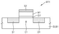
도 1은 본 발명의 실시예에 따른 비휘발성 메모리 트랜지스터를 보여주는 단면도이다.
도 2는 본 발명의 다른 실시예에 따른 비휘발성 메모리 트랜지스터를 보여주는 단면도이다.
도 3은 본 발명의 다른 실시예에 따른 비휘발성 메모리 트랜지스터를 보여주는 단면도이다.
도 4는 본 발명의 실시예에 따른 비휘발성 메모리 트랜지스터에 사용될 수 있는 이온종 이동층의 저항 변화 특성을 측정하기 위한 셀 구조를 보여주는 단면도이다.
도 5 및 도 6은 도 4의 구조에서 이온종 이동층의 인가 전압에 따른 저항 변화 특성을 보여주는 그래프이다.
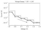
도 7 및 도 8은 도 4의 구조에 대한 전압 스윕(voltage sweep)에 따른 전류 변화를 보여주는 그래프이다.
도 9a 내지 도 9c는 이온종 이동층의 다양한 이온 분포를 예시적으로 보여주는 단면도이다.
도 10은 도 9a 내지 도 9c의 이온 분포 변화에 따른 이온종 이동층의 정전위(electrostatic potential) 변화를 보여주는 그래프이다.
도 11은 본 발명의 실시예에 따른 비휘발성 메모리 트랜지스터의 이온종 이동층의 이온종 이동에 따른 문턱전압 변화를 보여주는 그래프이다.
도 12는 본 발명의 실시예에 따른 비휘발성 메모리 트랜지스터의 이온종 이동층의 이온종 이동에 따른 문턱전압 변화를 보여주는 시뮬레이션 결과이다.
도 13은 종래의 SRAM(static random access memory)으로 16 레벨의 소자를 구성한 예를 보여주는 회로도이다.
도 14는 본 발명의 실시예에 따른 비휘발성 메모리 트랜지스터를 시냅스 소자에 적용하는 경우를 보여주는 개념도이다.
도 15는 본 발명의 실시예에 따른 비휘발성 메모리 트랜지스터를 포함하는 시냅스 소자를 보여주는 단면도이다.
도 16은 본 발명의 실시예에 따른 비휘발성 메모리 트랜지스터를 포함하는 시냅스 어레이 소자를 보여주는 회로도이다.
도 17은 본 발명의 실시예에 따른 시냅스 소자를 포함하는 뇌신경모사 소자(neuromorphic device)를 보여주는 사시도이다.
도 18은 도 17의 CMOS(complementary metal-oxide-semiconductor) 뉴런 회로의 구성을 예시적으로 보여주는 회로도이다.1 is a cross-sectional view illustrating a nonvolatile memory transistor according to an embodiment of the present invention.
2 is a cross-sectional view illustrating a nonvolatile memory transistor according to another exemplary embodiment of the present invention.
3 is a cross-sectional view illustrating a nonvolatile memory transistor according to another exemplary embodiment of the present invention.
4 is a cross-sectional view illustrating a cell structure for measuring resistance change characteristics of an ionic species moving layer that may be used in a nonvolatile memory transistor according to an exemplary embodiment of the present invention.
5 and 6 are graphs showing the resistance change characteristics of the ion species moving layer according to the applied voltage in the structure of FIG.
7 and 8 are graphs showing a change in current according to a voltage sweep for the structure of FIG. 4.
9A to 9C are cross-sectional views illustrating various ion distributions of an ion species moving bed.
FIG. 10 is a graph showing a change in the electrostatic potential of the ion species moving layer according to the ion distribution of FIGS. 9A to 9C.
FIG. 11 is a graph illustrating a change in threshold voltage according to ion species movement of an ion species moving layer of a nonvolatile memory transistor according to an exemplary embodiment of the present invention.
FIG. 12 is a simulation result showing threshold voltage changes according to ion species movement of an ion species moving layer of a nonvolatile memory transistor according to an exemplary embodiment of the present invention.
FIG. 13 is a circuit diagram illustrating an example of configuring a 16-level device using a conventional static random access memory (SRAM).
14 is a conceptual diagram illustrating a case where a nonvolatile memory transistor according to an embodiment of the present invention is applied to a synaptic device.
15 is a cross-sectional view illustrating a synaptic device including a nonvolatile memory transistor according to an embodiment of the present invention.
16 is a circuit diagram illustrating a synaptic array device including a nonvolatile memory transistor according to an embodiment of the present invention.
17 is a perspective view illustrating a neuromorphic device including a synaptic device according to an embodiment of the present invention.
FIG. 18 is a circuit diagram illustrating a configuration of a complementary metal-oxide-semiconductor (CMOS) neuron circuit of FIG. 17.
이하, 본 발명의 실시예들에 따른 비휘발성 메모리 트랜지스터, 이를 포함하는 소자 및 이들의 동작방법을 첨부된 도면을 참조하여 상세하게 설명한다. 첨부된 도면에 도시된 층이나 영역들의 폭 및 두께는 명세서의 명확성을 위해 다소 과장되게 도시된 것이다. 상세한 설명 전체에 걸쳐 동일한 참조번호는 동일한 구성요소를 나타낸다.Hereinafter, a nonvolatile memory transistor, a device including the same, and an operating method thereof according to embodiments of the present invention will be described in detail with reference to the accompanying drawings. The width and thickness of the layers or regions shown in the accompanying drawings are somewhat exaggerated for clarity. Like numbers refer to like elements throughout.
도 1은 본 발명의 실시예에 따른 비휘발성 메모리 트랜지스터(MT1)를 보여주는 단면도이다.1 is a cross-sectional view illustrating a nonvolatile memory transistor MT1 according to an exemplary embodiment of the present invention.
도 1을 참조하면, 채널요소(C1)가 구비되고, 채널요소(C1)에 대응하는 게이트전극(G1)이 구비될 수 있다. 채널요소(C1)와 게이트전극(G1) 사이에 게이트절연층(GI1)이 구비될 수 있다. 게이트절연층(GI1)과 게이트전극(G1) 사이에 이온종 이동층(ionic species moving layer or ionic species movable layer)(M1)이 구비될 수 있다. 채널요소(C1) 상에 게이트절연층(GI1), 이온종 이동층(M1) 및 게이트전극(G1)이 순차로 구비될 수 있다. 또한, 채널요소(C1)를 사이에 두고 서로 이격된 소오스(S1) 및 드레인(D1)이 구비될 수 있다. 소오스(S1) 및 드레인(D1)은 채널요소(C1)의 양단에 접촉될 수 있다. 소오스(S1), 드레인(D1) 및 채널요소(C1)는 기판(SUB1) 내에 구비될 수 있다. 예컨대, 게이트전극(G1) 양측의 기판(SUB1) 영역 내에 소정의 불순물을 주입하여 소오스(S1) 및 드레인(D1)을 형성할 수 있고, 소오스(S1)와 드레인(D1) 사이의 기판(SUB1) 영역이 채널요소(채널영역)(C1)으로 정의될 수 있다. 기판(SUB1)은, 예컨대, 실리콘(Si) 기판일 수 있다.Referring to FIG. 1, a channel element C1 may be provided and a gate electrode G1 corresponding to the channel element C1 may be provided. The gate insulating layer GI1 may be provided between the channel element C1 and the gate electrode G1. An ionic species moving layer or ionic species movable layer M1 may be provided between the gate insulating layer GI1 and the gate electrode G1. The gate insulating layer GI1, the ion species moving layer M1, and the gate electrode G1 may be sequentially provided on the channel element C1. In addition, a source S1 and a drain D1 spaced apart from each other with the channel element C1 interposed therebetween. The source S1 and the drain D1 may be in contact with both ends of the channel element C1. The source S1, the drain D1, and the channel element C1 may be provided in the substrate SUB1. For example, the source S1 and the drain D1 may be formed by implanting predetermined impurities into the region of the substrate SUB1 on both sides of the gate electrode G1, and the substrate SUB1 between the source S1 and the drain D1. ) Region may be defined as a channel element (channel region) C1. The substrate SUB1 may be, for example, a silicon (Si) substrate.
이온종 이동층(M1)은 소정의 이온종(ionic species)을 가질 수 있다. 예컨대, 상기 이온종은 산소 이온(oxygen ion) 및/또는 산소 공공(oxygen vacancy)을 포함할 수 있다. 이온종 이동층(M1)의 양단(상하 양단) 사이에 인가된 전압에 따라, 이온종 이동층(M1) 내에서 상기 이온종이 이동될 수 있다. 상기 이온종의 이동에 따라, 본 실시예에 따른 비휘발성 메모리 트랜지스터(MT1)의 문턱전압이 변화될 수 있다. 이와 관련해서, 비휘발성 메모리 트랜지스터(MT1)는 멀티-레벨(multi-level) 특성을 가질 수 있다. 예컨대, 비휘발성 메모리 트랜지스터(MT1)는 16 레벨 이상의 멀티-레벨(multi-level) 특성을 가질 수 있다.The ion species moving layer M1 may have a predetermined ionic species. For example, the ionic species may include oxygen ions and / or oxygen vacancy. According to the voltage applied between both ends (upper and lower ends) of the ion species moving layer M1, the ion species may be moved in the ion species moving layer M1. As the ion species moves, the threshold voltage of the nonvolatile memory transistor MT1 according to the present embodiment may change. In this regard, the nonvolatile memory transistor MT1 may have a multi-level characteristic. For example, the nonvolatile memory transistor MT1 may have a multi-level characteristic of 16 levels or more.
이온종 이동층(M1)은 저항성(resistive) 메모리 물질을 포함할 수 있다. 이 경우, 이온종 이동층(M1)은 산화물 저항체(oxide resistor)를 포함할 수 있다. 상기 산화물 저항체는 금속 산화물 저항체일 수 있고, 인가 전압에 따라 저항이 변하는 가변 저항 물질(variable resistance material)일 수 있다. 상기 가변 저항 물질은 바이폴라(bipolar) 메모리 물질일 수 있다. 구체적인 예로, 이온종 이동층(M1)은 PCMO(PrCaMnO), Ti 산화물, Ta 산화물, Ni 산화물, Zn 산화물, W 산화물, Co 산화물, Nb 산화물, TiNi 산화물, LiNi 산화물, InZn 산화물, V 산화물, SrZr 산화물, SrTi 산화물, Cr 산화물, Fe 산화물, Cu 산화물, Hf 산화물, Zr 산화물, Al 산화물 및 이들의 혼합물 중 적어도 어느 하나를 포함할 수 있다. 이 물질들은 형성 조건에 따라 유니폴라(unipolar) 또는 바이폴라(bipolar) 특징을 가질 수 있다. 본 실시예에서는 위 물질들의 바이폴라(bipolar) 특징을 이용할 수 있다. 또한, 상기한 물질들은 그 조성비에 따라 특성이 크게 변화될 수 있다. 따라서, 위 물질들은 저항 변화 특성 및/또는 바이폴라 특성을 나타낼 수 있는 조성비를 갖는 것으로 해석되어야 한다. 일례로, Al 산화물의 경우, Al2O3와 같이 화학양론적 조성을 갖는 산화물은 유전체(절연체) 특성을 갖고, 저항 변화 특성 및/또는 바이폴라 특성을 나타내지 않을 수 있다. 따라서, 상기한 Al 산화물은 저항 변화 특성 및/또는 바이폴라 특성을 나타낼 수 있는 비화학양론적 조성을 갖는 것으로 해석될 수 있다. 이는 전술한 다른 물질에 대해서도 유사하게 적용될 수 있다. 한편, 이온종 이동층(M1)의 두께는 10∼100nm 정도, 예컨대, 20∼80nm 정도일 수 있다.The ion species moving layer M1 may include a resistive memory material. In this case, the ion species moving layer M1 may include an oxide resistor. The oxide resistor may be a metal oxide resistor, and may be a variable resistance material whose resistance changes according to an applied voltage. The variable resistance material may be a bipolar memory material. As a specific example, the ionic species moving layer M1 may include PCMO (PrCaMnO), Ti oxide, Ta oxide, Ni oxide, Zn oxide, W oxide, Co oxide, Nb oxide, TiNi oxide, LiNi oxide, InZn oxide, V oxide, SrZr Oxide, SrTi oxide, Cr oxide, Fe oxide, Cu oxide, Hf oxide, Zr oxide, Al oxide and mixtures thereof. These materials may have unipolar or bipolar characteristics depending on the formation conditions. In this embodiment, the bipolar characteristics of the above materials can be used. In addition, the above-described materials may be significantly changed in properties depending on the composition ratio. Therefore, the above materials should be interpreted as having a composition ratio capable of exhibiting resistance change characteristics and / or bipolar characteristics. For example, in the case of Al oxide, an oxide having a stoichiometric composition such as Al2 O3 may have a dielectric (insulator) characteristic and may not exhibit resistance change characteristics and / or bipolar characteristics. Thus, the Al oxide can be interpreted as having a non-stoichiometric composition that can exhibit resistance change characteristics and / or bipolar characteristics. This may similarly apply to the other materials described above. Meanwhile, the thickness of the ion species moving layer M1 may be about 10 to 100 nm, for example, about 20 to 80 nm.
도 1에서 게이트전극(G1)에 인가된 전압과 기판(SUB1)의 몸체부(body)에 인가된 전압의 차이(이하, 전압차)에 의해 이온종 이동층(M1)의 상하 양단 사이에 전압이 인가될 수 있다. 상기 전압차에 해당하는 전압은 게이트절연층(GI1)과 이온종 이동층(M1)에 분산되어 인가될 수 있다. 이온종 이동층(M1)에 인가된 전압에 의해 이온종 이동층(M1) 내에서 이온종이 이동될 수 있다. 기판(SUB1)의 몸체부(body)에 소정의 전압이 일정하게 인가되고 있다고 가정하면, 게이트전극(G1)에 인가된 전압에 의해 이온종 이동층(M1) 내에서 이온종이 이동된다고 할 수 있다. 다른 측면에서 설명하면, 이온종 이동층(M1)의 상하 양단 사이에 인가된 전기장(electric field)에 의해 이온종 이동층(M1)의 이온종이 이동될 수 있다. 상기 전기장은 게이트전극(G1)에 인가된 전압에 의해 발생할 수 있다.In FIG. 1, the voltage between the upper and lower ends of the ionic species moving layer M1 due to the difference between the voltage applied to the gate electrode G1 and the voltage applied to the body of the substrate SUB1 (hereinafter, referred to as a voltage difference). Can be applied. The voltage corresponding to the voltage difference may be distributed and applied to the gate insulating layer GI1 and the ion species moving layer M1. Ion species may be moved in the ion species moving layer M1 by a voltage applied to the ion species moving layer M1. Assuming that a predetermined voltage is constantly applied to the body of the substrate SUB1, it can be said that ionic species are moved in the ion species moving layer M1 by the voltage applied to the gate electrode G1. . In another aspect, the ionic species of the ionic species moving layer M1 may be moved by an electric field applied between the upper and lower ends of the ionic species moving layer M1. The electric field may be generated by the voltage applied to the gate electrode G1.
본 발명의 다른 실시예에 따르면, 게이트절연층(GI1)과 이온종 이동층(M1) 사이에 "도전층"을 더 구비시킬 수 있다. 그 일례가 도 2에 도시되어 있다.According to another embodiment of the present invention, a "conductive layer" may be further provided between the gate insulating layer GI1 and the ion species moving layer M1. One example is shown in FIG.
도 2를 참조하면, 비휘발성 메모리 트랜지스터(MT2)는 게이트절연층(GI1)과 이온종 이동층(M1) 사이에 구비된 도전층(E1)을 더 포함할 수 있다. 도전층(E1)은 일종의 전극층일 수 있고, 금속이나 금속화합물 등으로 형성될 수 있다. 이온종 이동층(M1)은 두 개의 전극(E1, G1) 사이에 구비된 것으로 볼 수 있다. 이와 같이 도전층(E1)을 구비시킨 경우, 이온종 이동층(M1)에 대한 전압 인가(또는 전기장 인가)가 용이해질 수 있다. 따라서, 이온종 이동층(M1)의 이온종 이동이 용이해질 수 있다.Referring to FIG. 2, the nonvolatile memory transistor MT2 may further include a conductive layer E1 provided between the gate insulating layer GI1 and the ion species moving layer M1. The conductive layer E1 may be a kind of electrode layer, and may be formed of a metal, a metal compound, or the like. The ion species moving layer M1 may be regarded as being disposed between the two electrodes E1 and G1. When the conductive layer E1 is provided in this manner, voltage application (or electric field application) to the ion species moving layer M1 may be facilitated. Therefore, the ion species movement of the ion species moving layer M1 may be facilitated.
도 1 및 도 2의 이온종 이동층(M1) 내에서 이온종(예컨대, 산소 이온 및/또는 산소 공공)이 이동함에 따라, 이온종 이동층(M1)의 정전위(electrostatic potential)가 달라질 수 있고, 그에 따라, 비휘발성 메모리 트랜지스터(MT1, MT2)의 문턱전압이 변화될 수 있다. 다시 말해, 이온종 이동층(M1) 내에서 이온종이 이동함에 따라, 이온종 이동층(M1)의 이온종 분포가 변화되고, 채널요소(C1)에 대한 이온종 이동층(M1)의 전기적 영향이 변화될 수 있다. 그 결과, 비휘발성 메모리 트랜지스터(MT1, MT2)의 문턱전압이 변화될 수 있다. 상기 이온종이 음(-)의 이온종인 경우, 이온종 이동층(M1) 내에서 상기 음(-)의 이온종의 농도가 게이트절연층(GI1) 측으로 증가할수록 문턱전압은 증가할 수 있다. 상기 이온종이 양(+)의 이온종인 경우, 이온종 이동층(M1) 내에서 상기 양(+)의 이온종의 농도가 게이트절연층(GI1) 측으로 증가할수록 문턱전압은 감소할 수 있다. 이온종 이동층(M1) 내에서 상기 이온종의 이동은 점진적으로(continuous-like or gradually) 그리고 가역적으로 이루어질 수 있다. 따라서, 비휘발성 메모리 트랜지스터(MT1, MT2)의 문턱전압도 점진적으로 그리고 가역적으로 변화될 수 있다. 다른 측면에서 설명하면, 이온종 이동층(M1)의 상하 양단 사이에 인가된 전기장(electric field)에 의해 이온종 이동층(M1)의 이온종이 이동할 수 있고, 그 결과, 이온종 이동층(M1) 내에 내부 전계(internal electric field)가 유발 또는 변화될 수 있다. 이온종 이동에 따라, 상기 내부 전계의 세기도 달라질 수 있다. 상기 내부 전계는 점진적으로 그리고 가역적으로 변화될 수 있다. 이러한 내부 전계의 변화에 의해 비휘발성 메모리 트랜지스터(MT1, MT2)의 문턱전압이 변화될 수 있다. 또한, 상기 이온종의 이동에 따라, 이온종 이동층(M1)의 소정 영역의 캐패시턴스(capacitance)가 변화될 수 있고, 이러한 캐패시턴스의 변화에 의해 문턱전압이 변화되는 것으로 여길 수도 있다. 이온종 이동층(M1)의 이온종 이동에 따른 문턱전압의 변화에 대해서는 추후에 보다 상세히 설명한다.As the ion species (eg, oxygen ions and / or oxygen vacancies) move in the ion species moving layer M1 of FIGS. 1 and 2, the electrostatic potential of the ion species moving layer M1 may vary. As a result, the threshold voltages of the nonvolatile memory transistors MT1 and MT2 may be changed. In other words, as the ionic species move in the ionic species moving layer M1, the ionic species distribution of the ionic species moving layer M1 changes, and the electrical effect of the ion species moving layer M1 on the channel element C1 is changed. This can be changed. As a result, the threshold voltages of the nonvolatile memory transistors MT1 and MT2 may be changed. When the ion species are negative ion species, the threshold voltage may increase as the concentration of the negative ion species in the ion species moving layer M1 increases toward the gate insulating layer GI1. When the ionic species is a positive ionic species, the threshold voltage may decrease as the concentration of the positive ionic species increases in the ion insulating layer M1 toward the gate insulating layer GI1. The movement of the ionic species in the ionic species moving bed M1 can be made continuously or like and gradually. Therefore, the threshold voltages of the nonvolatile memory transistors MT1 and MT2 may also be gradually and reversibly changed. In another aspect, the ionic species of the ionic species moving layer M1 may move by an electric field applied between the upper and lower ends of the ionic species moving layer M1, and as a result, the ionic species moving layer M1 An internal electric field may be induced or changed in the X-rays. As the ion species moves, the strength of the internal electric field may also vary. The internal electric field can be changed gradually and reversibly. Due to the change in the internal electric field, the threshold voltages of the nonvolatile memory transistors MT1 and MT2 may be changed. In addition, as the ionic species moves, capacitance of a predetermined region of the ionic species moving layer M1 may change, and it may be considered that the threshold voltage changes due to the change of capacitance. The change in the threshold voltage according to the ion species movement of the ion species moving layer M1 will be described in more detail later.
본 발명의 다른 실시예에 따르면, 도 1 및 도 2의 구조에서 이온종 이동층(M1)을 다층 구조로 형성할 수 있다. 그 일례가 도 3에 도시되어 있다. 도 3은 도 2의 이온종 이동층(M1)이 다층 구조를 갖는 경우이다.According to another exemplary embodiment of the present invention, the ion species moving layer M1 may be formed in a multilayer structure in the structures of FIGS. 1 and 2. An example is shown in FIG. 3. 3 illustrates a case in which the ion species moving layer M1 of FIG. 2 has a multilayer structure.
도 3을 참조하면, 비휘발성 메모리 트랜지스터(MT3)는 다층 구조의 이온종 이동층(M2)을 포함할 수 있다. 이온종 이동층(M2)은, 예컨대, 이중층 구조를 가질 수 있다. 이 경우, 이온종 이동층(M2)은 제1 물질층(10) 및 제2 물질층(20)을 포함할 수 있다. 제1 물질층(10) 내에 산소 이온 및/또는 산소 공공(vacancy)이 존재할 수 있다. 이러한 제1 물질층(10)은 제2 물질층(20)에 대하여 "산소공급층"(oxygen supplying layer)으로 작용할 수 있다. 제1 물질층(10)은 "산소저장층"(oxygen reservoir layer)이라고 할 수도 있다. 제2 물질층(20)은 제1 물질층(10)과 유사하게 산소 이온 및/또는 산소 공공(vacancy)을 포함할 수 있다. 제2 물질층(20)은 제1 물질층(10)과 산소 이온 및/또는 산소 공공(vacancy)을 주고 받으며, 이온종 이동층(M1)의 저항 변화를 유도하는 층일 수 있다. 이런 점에서, 제2 물질층(20)은 "산소교환층"(oxygen exchange layer)이라 할 수 있다. 제2 물질층(20)의 산소 농도는 제1 물질층(10)의 산소 농도보다 높을 수 있다.Referring to FIG. 3, the nonvolatile memory transistor MT3 may include an ion species moving layer M2 having a multilayer structure. The ion species moving layer M2 may have, for example, a double layer structure. In this case, the ion species moving layer M2 may include the
도 4는 본 발명의 실시예에 따른 비휘발성 메모리 트랜지스터에 사용될 수 있는 이온종 이동층의 저항 변화 특성을 측정하기 위한 셀 구조를 보여준다.4 illustrates a cell structure for measuring resistance change characteristics of an ionic species moving layer that can be used in a nonvolatile memory transistor according to an exemplary embodiment of the present invention.
도 4를 참조하면, 이온종 이동층(M10)이 두 전극(이하, 제1 및 제2 전극)(E10, E20) 사이에 구비되어 있다. 이온종 이동층(M10)은 다량의 산소 이온을 가질 수 있다. 산소 이온은 제1 및 제2 전극(E10, E20) 사이에 인가된 전압에 의해 이동할 수 있다. 예컨대, 제1 전극(E10)에 양(+)의 전압이 인가되고, 제2 전극(E20)에 음(-)의 전압이 인가되면, 산소 이온들은 제1 전극(E10) 측으로 어느 정도 이동할 수 있다. 반대로, 제1 전극(E10)에 음(-)의 전압이 인가되고, 제2 전극(E20)에 양(+)의 전압이 인가되면, 산소 이온들은 제2 전극(E20) 측으로 어느 정도 이동할 수 있다. 만약, 동일한 전압 신호가 반복해서 두 전극(E10, E20) 사이에 인가되면, 상기 신호가 인가된 횟수만큼 산소 이온들이 어느 한 방향으로 점진적으로(누적하여) 이동할 수 있다. 이온종 이동층(M10)의 산소 공공(vacancy)(미도시)은 산소 이온과 반대 방향으로 이동할 수 있다. 산소 이온은 음(-)의 전하를 갖는다고 할 수 있고, 산소 공공은 양(+)의 전하를 갖는다고 할 수 있다.Referring to FIG. 4, an ion species moving layer M10 is provided between two electrodes (hereinafter, first and second electrodes) E10 and E20. The ion species moving layer M10 may have a large amount of oxygen ions. Oxygen ions may be moved by a voltage applied between the first and second electrodes E10 and E20. For example, when a positive voltage is applied to the first electrode E10 and a negative voltage is applied to the second electrode E20, oxygen ions may move to the first electrode E10 to some extent. have. On the contrary, when a negative voltage is applied to the first electrode E10 and a positive voltage is applied to the second electrode E20, oxygen ions may move to the second electrode E20 to some extent. have. If the same voltage signal is repeatedly applied between the two electrodes E10 and E20, oxygen ions may gradually (accumulate) move in either direction by the number of times the signal is applied. Oxygen vacancy (not shown) of the ion species moving layer M10 may move in the opposite direction to the oxygen ions. Oxygen ions can be said to have a negative charge, and oxygen vacancies can be said to have a positive charge.
도 5 및 도 6은 본 발명의 실시예에 따른 비휘발성 메모리 트랜지스터에 사용될 수 있는 이온종 이동층의 인가 전압에 따른 저항 변화 특성을 보여주는 그래프이다. 도 5 및 도 6은 도 4의 구조에 대한 전압-전류 특성 변화를 보여준다. 도 5는 도 4의 이온종 이동층(M10)이 PCMO층인 경우이고, 도 6은 도 4의 이온종 이동층(M10)이 TaOx층인 경우이다. 도 5는 온/오프(ON/OFF) 동작, 즉, 세트/리세트(set/reset) 동작을 반복하면서 측정한 결과를 보여주고, 도 6은 한 번의 온/오프(ON/OFF) 스윕(sweep) 동작에 대한 결과를 보여준다.5 and 6 are graphs illustrating resistance change characteristics according to an applied voltage of an ionic species moving layer that may be used in a nonvolatile memory transistor according to an exemplary embodiment of the present invention. 5 and 6 show changes in voltage-current characteristics for the structure of FIG. 5 illustrates a case where the ion species moving layer M10 of FIG. 4 is a PCMO layer, and FIG. 6 illustrates a case where the ion species moving layer M10 of FIG. 4 is a TaOx layer. FIG. 5 shows a measurement result by repeating an ON / OFF operation, that is, a set / reset operation, and FIG. 6 shows a single ON / OFF sweep ( sweep) shows the results of the operation.
도 5를 참조하면, 저항 변화 그래프의 커런트(current) 레벨이 여러 개로 나눠지는 것을 확인할 수 있다. 이는 이온종 이동층(M10)이 멀티-레벨 특성을 가질 수 있다는 것을 의미한다. 또한, PCMO층의 저항 변화는 약 ±4.0 V 이내의 범위 내에서 이루어지는 것을 알 수 있다.Referring to FIG. 5, it can be seen that the current level of the resistance change graph is divided into several. This means that the ionic species moving layer M10 may have multi-level characteristics. In addition, it can be seen that the resistance change of the PCMO layer is made within a range of about ± 4.0V.
도 6을 참조하면, TaOx층의 저항 변화가 ±2.5V 이내의 전압 범위 내에서 이루어지는 것을 알 수 있다. 이는 이온종 이동층(M10)의 저항 변화가 ±2.5 V 이내의 저전압 범위에서 이루어질 수 있음을 의미한다.Referring to FIG. 6, it can be seen that the resistance change of the TaOx layer is made within a voltage range within ± 2.5V. This means that the resistance change of the ion species moving layer M10 may be made in the low voltage range within ± 2.5V.
도 7 및 도 8은 도 4의 구조에 대한 전압 스윕(voltage sweep)에 따른 전류 변화를 보여주는 그래프이다. 도 7은 두 전극(E10, E20) 사이의 전압을 1.9 V 에서 2.4 V 로 증가시키면서 전류 변화를 측정한 결과이고, 도 8은 두 전극(E10, E20) 사이의 전압을 -0.8 V 에서 -1.6 V 로 증가(절대값 증가)시키면서 전류 변화를 측정한 결과이다.7 and 8 are graphs showing a change in current according to a voltage sweep for the structure of FIG. 4. 7 is a result of measuring the current change while increasing the voltage between the two electrodes (E10, E20) from 1.9 V to 2.4 V, Figure 8 shows the voltage between the two electrodes (E10, E20) from -0.8 V to -1.6 This is the result of measuring the current change while increasing with V (absolute value increase).
도 7 및 도 8을 참조하면, 전압 스윕(voltage sweep)에 따라 전류가 점진적으로 감소하거나 증가하는 것을 알 수 있다. 이는 전압 스윕(voltage sweep) 방향에 따라, 도 4 구조의 저항이 점차 증가하거나 감소할 수 있음을 의미한다.Referring to FIGS. 7 and 8, it can be seen that the current gradually decreases or increases according to the voltage sweep. This means that, depending on the direction of the voltage sweep, the resistance of the FIG. 4 structure may gradually increase or decrease.
도 9a 내지 도 9c는 이온종 이동층(M10)의 다양한 이온 분포를 예시적으로 보여주는 단면도이다. 도 9a에서 도 9c로 갈수록 산소 이온이 위쪽으로(즉, 상면측으로) 축적되는 것을 알 수 있다. 이온종 이동층(M10) 내에서 산소 이온의 분포가 달라진다는 것은 소정 영역에서 산소 이온의 밀도가 변화된다는 것을 의미한다. 이온종 이동층(M10)에 인가된 전압에 따라, 이온종 이동층(M10)의 이온 분포가 점진적으로 변화될 수 있다.9A to 9C are cross-sectional views illustrating various ion distributions of the ion species moving layer M10. It can be seen from FIG. 9A to FIG. 9C that oxygen ions accumulate upward (that is, to the upper surface side). The change in the distribution of oxygen ions in the ion species moving layer M10 means that the density of oxygen ions is changed in a predetermined region. According to the voltage applied to the ion species moving layer M10, the ion distribution of the ion species moving layer M10 may be gradually changed.
도 10은 도 9a 내지 도 9c의 이온 분포 변화에 따른 이온종 이동층(M10)의 정전위(electrostatic potential) 변화를 보여주는 그래프이다. 도 10의 (a), (b), (c) 그래프는 각각 도 9a, 도 9b 및 도 9c에 대응된다. 도 10의 결과로부터, 이온 분포 변화에 따라 정전위가 점진적으로 변화되는 것을 확인할 수 있다.FIG. 10 is a graph showing a change in electrostatic potential of the ion species moving layer M10 according to the change in ion distribution of FIGS. 9A to 9C. The graphs of FIGS. 10A, 10B, and 9C correspond to FIGS. 9A, 9B, and 9C, respectively. From the results in FIG. 10, it can be seen that the potential is gradually changed as the ion distribution changes.
도 11은 본 발명의 실시예에 따른 비휘발성 메모리 트랜지스터의 이온종 이동층의 이온종 이동에 따른 문턱전압 변화를 보여주는 그래프이다.FIG. 11 is a graph illustrating a change in threshold voltage according to ion species movement of an ion species moving layer of a nonvolatile memory transistor according to an exemplary embodiment of the present invention.
도 11을 참조하면, 이온종 이동층(도 1 및 도 2의 M1)의 채널영역에 가까운 부분(여기서는, 하단부)에 산소 이온이 많아질수록 문턱전압은 양(+)의 방향으로 점진적으로 증가할 수 있다. 이는 이온종 이동층(M1)의 채널영역에 가까운 부분에 산소 이온이 많아질수록 채널영역에 양(+)의 전하가 축적될 수 있고, 결과적으로, n-채널을 형성하는데 더 높은 전압이 요구되기 때문이다. 도 11에서 산소 이온의 다소(많고 적음)는 산소 공공의 다소(많고 적음)와 반대이다. 그러므로, 이온종 이동층(M1)의 채널영역에 가까운 부분(여기서는, 하단부)에 산소 공공의 양이 적어질수록 문턱전압은 양(+)의 방향으로 점진적으로 증가할 수 있다. 산소 이온이나 산소 공공이 점진적으로 이동함에 따라, 문턱전압도 그에 대응하여 점진적으로 변화될 수 있고, 이러한 이온종의 이동 및 문턱전압 변화는 "비휘발성"을 가질 수 있다. 즉, 전압을 인가하여 이온종을 이동시키면, 상기 전압을 제거하여도, 최종 상태가 지속적으로 유지될 수 있다.Referring to FIG. 11, the threshold voltage gradually increases in the positive direction as the amount of oxygen ions increases in the portion close to the channel region of the ion species moving layer M1 of FIGS. 1 and 2 (here, the lower end portion). can do. This is because the more oxygen ions are in the portion closer to the channel region of the ion species moving layer M1, the positive charges can accumulate in the channel region, and as a result, a higher voltage is required to form the n-channel. Because it becomes. In Figure 11 some (more and less) of oxygen ions are opposite to some (more and less) of oxygen vacancies. Therefore, as the amount of oxygen vacancies in the portion close to the channel region (here, the lower end portion) of the ion species moving layer M1 decreases, the threshold voltage may gradually increase in the positive direction. As oxygen ions or oxygen vacancies gradually move, the threshold voltage may also change gradually correspondingly, and the movement and threshold voltage change of these ionic species may have "non-volatile". That is, when the ion species is moved by applying a voltage, the final state can be maintained continuously even when the voltage is removed.
도 12는 본 발명의 실시예에 따른 비휘발성 메모리 트랜지스터의 이온종 이동층의 이온종 이동에 따른 문턱전압 변화를 보여주는 시뮬레이션(simulation) 결과이다. 양(+)의 이온종을 채널영역 쪽으로 이동시키면서 또는 게이트전극 쪽으로 이동시키면서 게이트전압(Vg)-드레인전류(Id) 특성을 평가하였다.FIG. 12 is a simulation result illustrating variation of a threshold voltage according to ion species movement of an ion species moving layer of a nonvolatile memory transistor according to an exemplary embodiment of the present invention. The gate voltage (Vg) -drain current (Id) characteristics were evaluated while moving the positive ion species toward the channel region or toward the gate electrode.
도 12를 참조하면, 양(+)의 이온종(즉, positive charge)이 게이트전극에 가까이 이동할수록 메모리 트랜지스터의 문턱전압은 점차 증가하였다. 양(+)의 이온종이 채널영역에 가까이 이동할수록 문턱전압은 점차 감소하였다. 이러한 결과는 도 11의 그래프와 유사하다. 또한, 도 12의 그래프에서는 소정의 게이트전압, 예컨대, 1V의 게이트전압에서 멀티-레벨(multi-level)의 드레인전류가 출력되는 것을 알 수 있다. 문턱전압의 변화에 따라, 멀티-레벨의 드레인전류가 출력될 수 있다.Referring to FIG. 12, as the positive ion species (ie, positive charge) move closer to the gate electrode, the threshold voltage of the memory transistor gradually increases. As the positive ion species moved closer to the channel region, the threshold voltage gradually decreased. This result is similar to the graph of FIG. In addition, it can be seen from the graph of FIG. 12 that a multi-level drain current is output at a predetermined gate voltage, for example, a gate voltage of 1V. According to the change of the threshold voltage, a multi-level drain current can be output.
본 발명의 실시예에 따른 비휘발성 메모리 트랜지스터는 낮은 동작전압(예컨대, 약 ±5.0 V 이내의 동작전압)을 가지면서 동시에 작은 사이즈에서도 충분히 큰 멀티-레벨(multi-level) 특성을 나타낼 수 있다. 즉, 도 5 및 도 6에서 설명한 바와 같이, 이온종 이동층의 저항 변화는 약 ±4.0 V 이내 또는 약 ±2.5 V 이내의 저전압 범위에서 이루어질 수 있으므로, 상기 비휘발성 메모리 트랜지스터는 낮은 전압 범위에서 동작될 수 있다. 또한, 이온종 이동층의 이온종을 점진적으로 이동시킴으로써, 도 11 및 도 12에서 설명한 바와 같이, 메모리 트랜지스터의 문턱전압이 점진적으로 변화되기 때문에, 16 레벨 이상의 멀티-레벨(multi-level) 특성을 용이하게 구현할 수 있다.A nonvolatile memory transistor according to an embodiment of the present invention may have a low operating voltage (for example, an operating voltage within about ± 5.0 V) and at the same time exhibit a sufficiently large multi-level characteristic even in a small size. That is, as described with reference to FIGS. 5 and 6, the resistance change of the ion species moving layer may be made in a low voltage range of about ± 4.0 V or within about ± 2.5 V, so that the nonvolatile memory transistor operates in a low voltage range. Can be. In addition, by gradually moving the ion species of the ion species moving layer, as described with reference to FIGS. 11 and 12, since the threshold voltage of the memory transistor is gradually changed, multi-level characteristics of 16 levels or more are obtained. It can be easily implemented.
플래시 메모리의 경우, 전자의 터널 주입(tunnel injection)을 이용하기 때문에, 동작전압이 10∼20 V 정도로 높은 단점이 있다. 또한, 플로팅 게이트에 트랩(trap) 되는 전자의 수가 제한적이기 때문에, 멀티-비트(multi-bit) 특성을 구현하기 어려운 문제가 있다. 그러나, 본 발명의 실시예에 따르면, 상기한 플래시 메모리의 문제점들을 극복하고, 저전압 영역에서 동작되면서 작은 사이즈로도 충분히 큰 멀티-레벨(multi-level) 특성을 나타내는 비휘발성 소자를 구현할 수 있다.In the case of flash memory, since the tunnel injection of the electron (tunnel injection) is used, there is a disadvantage that the operating voltage is as high as 10 ~ 20V. In addition, since the number of electrons trapped in the floating gate is limited, it is difficult to realize a multi-bit characteristic. However, according to the embodiment of the present invention, it is possible to overcome the above-described problems of the flash memory and to implement a nonvolatile device having a multi-level characteristic that is sufficiently large even in a small size while operating in a low voltage region.
도 13은 종래의 SRAM(static random access memory)으로 16 레벨(4 bit)의 소자를 구성한 예를 보여주는 회로도이다.FIG. 13 is a circuit diagram illustrating an example of configuring a 16-level (4 bit) device using a conventional static random access memory (SRAM).
도 13을 참조하면, 종래의 SRAM으로 16 레벨(4 비트)의 소자를 구성하려면, 16개의 SRAM이 필요하고, 이와 더불어 주변회로(미도시)가 요구된다. 그리고, 각각의 SRAM은 6개의 트랜지스터를 포함한다. 따라서, 종래의 SRAM으로 16 레벨(4 비트)의 소자를 구성하려면, 최소 96개의 트랜지스터가 요구된다.Referring to FIG. 13, in order to configure a device having 16 levels (4 bits) of a conventional SRAM, 16 SRAMs are required, and a peripheral circuit (not shown) is required. And each SRAM includes six transistors. Therefore, at least 96 transistors are required to construct a 16-level (4-bit) device with a conventional SRAM.
그러나, 본 발명의 실시예에 따른 비휘발성 메모리 트랜지스터는, 하나의 트랜지스터만으로 16 레벨 이상의 멀티-레벨을 구현할 수 있다. 따라서, 본 발명의 실시예에 따른 비휘발성 메모리 트랜지스터를 사용하여 소정의 회로를 구성할 경우, 필요한 단위 소자의 수를 획기적으로 줄일 수 있고, 회로의 구성을 단순화할 수 있으며, 전체 시스템의 사이즈를 크게 줄일 수 있다.However, the nonvolatile memory transistor according to the embodiment of the present invention can implement multi-level of 16 levels or more with only one transistor. Therefore, when a predetermined circuit is configured using the nonvolatile memory transistor according to the embodiment of the present invention, the number of required unit elements can be significantly reduced, the circuit configuration can be simplified, and the size of the entire system can be reduced. Can be greatly reduced.
본 발명의 실시예에 따른 비휘발성 메모리 트랜지스터는 다양한 전자장치 및 논리소자 등에 여러 가지 목적으로 사용될 수 있다. 특히, 상기 비휘발성 메모리 트랜지스터는 시냅스(synapse) 소자/회로에 적용될 수 있다. 시냅스는 뇌신경 세포 간을 연결하는 연접부로, 학습과 기억에 중요한 역할을 한다. 시냅스를 통해 전달 신호가 흐를 때마다 시냅스가 강화되는 것과 마찬가지로, 본 실시예의 비휘발성 메모리 트랜지스터의 게이트전극에 전압이 가해지면 이온종 이동층의 전기적 특성이 변화되면서 트랜지스터의 문턱전압이 점진적으로(누적하여) 변화될 수 있다. 또한, 문턱전압의 변화는 "비휘발성"을 가질 수 있다. 따라서, 본 발명의 실시예들에 따른 비휘발성 메모리 트랜지스터는 시냅스 소자/회로에 적용될 수 있다. 상기 비휘발성 메모리 트랜지스터는 16 레벨 이상의 멀티-레벨 특성을 가질 수 있고, 또한 저전압 범위에서 동작할 수 있기 때문에, 이를 이용하여 시냅스 소자/회로를 구성할 경우, 소자/회로의 크기를 크게 줄일 수 있고 소비 전력을 낮출 수 있다. 또한, 저전압에서 동작되기 때문에, 신뢰성을 높일 수 있다.The nonvolatile memory transistor according to the embodiment of the present invention can be used for various purposes such as various electronic devices and logic devices. In particular, the nonvolatile memory transistor can be applied to a synapse device / circuit. Synapses are the junctions between brain cells, which play an important role in learning and memory. Just as the synapse is intensified every time a transmission signal flows through the synapse, when the voltage is applied to the gate electrode of the nonvolatile memory transistor of the present embodiment, the electrical characteristics of the ion-type moving layer are changed and the threshold voltage of the transistor is gradually (cumulative) Can be changed). In addition, the change in the threshold voltage may have a "non-volatile". Thus, the nonvolatile memory transistor according to the embodiments of the present invention can be applied to a synapse device / circuit. Since the nonvolatile memory transistor may have a multi-level characteristic of 16 levels or more and operate in a low voltage range, when the synaptic device / circuit is configured using the nonvolatile memory transistor, the size of the device / circuit may be greatly reduced. The power consumption can be lowered. In addition, since it is operated at a low voltage, reliability can be improved.
도 14는 본 발명의 실시예에 따른 비휘발성 메모리 트랜지스터(MT10)를 시냅스 소자에 적용하는 경우를 보여주는 개념도이다.14 is a conceptual diagram illustrating a case where a nonvolatile memory transistor MT10 according to an embodiment of the present invention is applied to a synaptic device.
도 14를 참조하면, 프리-뉴런(pre-neuron)과 포스트-뉴런(post-neuron) 사이의 연결부인 시냅스를 회로적으로 구성할 때, 본 발명의 실시예에 따른 비휘발성 메모리 트랜지스터(MT10)를 적용할 수 있다. 프리-뉴런(pre-neuron)은 프리-스파이크(pre-spike) 신호를 시냅스에 입력할 수 있고, 시냅스는 소정의 시냅틱 신호(synaptic signal)를 포스트-뉴런(post-neuron)으로 전달할 수 있으며, 포스트-뉴런(post-neuron)은 포스트-스파이크(post-spike) 신호를 발생할 수 있다. 시냅스가 프리-뉴런(pre-neuron)과 포스트-뉴런(post-neuron)을 연결하는 것과 유사하게, 비휘발성 메모리 트랜지스터(MT10)는 프리-시냅틱 뉴런 회로(pre-synaptic neuron circuit)와 포스트-시냅틱 뉴런 회로(post-synaptic neuron circuit)를 연결하는 역할을 할 수 있다. 이러한 구성을 회로적으로 도시하면 도 15와 같을 수 있다.Referring to FIG. 14, when constructing a synapse that is a connection between a pre-neuron and a post-neuron in a circuit, a nonvolatile memory transistor MT10 according to an embodiment of the present invention. Can be applied. Pre-neurons can input pre-spike signals to the synapses, synapses can deliver certain synaptic signals to post-neurons, Post-neurons may generate post-spike signals. Similar to synapses connecting pre-neurons and post-neurons, non-volatile memory transistors (MT10s) are characterized by pre-synaptic neuron circuits and post-synaptic It can play a role in connecting the post-synaptic neuron circuit. Such a configuration may be as shown in FIG. 15.
도 15를 참조하면, 비휘발성 메모리 트랜지스터(MT10)의 게이트전극(G1)은 프리-시냅틱 뉴런 회로(pre-synaptic neuron circuit)(N1)에 연결될 수 있다. 비휘발성 메모리 트랜지스터(MT10)의 소오스(S1)는 포스트-시냅틱 뉴런 회로(post-synaptic neuron circuit)(N2)에 연결될 수 있다. 프리-시냅틱 뉴런 회로(pre-synaptic neuron circuit)(N1)로부터 프리-스파이크(pre-spike) 신호가 게이트전극(G1)에 인가될 수 있고, 소오스(S1)를 통해 포스트-시냅틱 전류(post-synaptic current)가 포스트-시냅틱 뉴런 회로(post-synaptic neuron circuit)(N2)로 흐를 수 있다. 포스트-시냅틱 뉴런 회로(post-synaptic neuron circuit)(N2)로부터 포스트-스파이크(post-spike) 신호가 발생할 수 있다. 한편, 트랜지스터(MT10)의 드레인(D1)에는 소정의 전압(VDS)이 일정하게 인가될 수 있다. 즉, 소정의 정전압(constant voltage)(VDS)이 드레인(D1)에 인가될 수 있다.Referring to FIG. 15, the gate electrode G1 of the nonvolatile memory transistor MT10 may be connected to a pre-synaptic neuron circuit N1. The source S1 of the nonvolatile memory transistor MT10 may be connected to a post-synaptic neuron circuit N2. A pre-spike signal can be applied to the gate electrode G1 from a pre-synaptic neuron circuit N1 and a post-synaptic current through the source S1. synaptic currents can flow into the post-synaptic neuron circuit (N2). Post-spike signals may be generated from the post-synaptic neuron circuit N2. Meanwhile, a predetermined voltage VDS may be constantly applied to the drain D1 of the transistor MT10. That is, a predetermined constant voltage VDS may be applied to the drain D1.
게이트전극(G1)에 프리-스파이크(pre-spike) 신호가 반복해서 인가됨에 따라, 트랜지스터(MT10)의 문턱전압이 양(+)의 방향 또는 음(-)의 방향으로 점진적으로 변화될 수 있고, 문턱전압의 변화가 소정의 임계점을 넘어가면, 프리-스파이크(pre-spike) 신호에 의해 트랜지스터(MT10)가 턴-온(turn-on) 될 수 있다. 이때, 소오스(S1)를 통해 포스트-시냅틱 전류(post-synaptic current)가 포스트-시냅틱 뉴런 회로(post-synaptic neuron circuit)(N2)로 흐를 수 있다.As the pre-spike signal is repeatedly applied to the gate electrode G1, the threshold voltage of the transistor MT10 may be gradually changed in the positive direction or the negative direction. When the change in the threshold voltage exceeds a predetermined threshold, the transistor MT10 may be turned on by the pre-spike signal. At this time, a post-synaptic current may flow through the source S1 to a post-synaptic neuron circuit N2.
도 16은 본 발명의 실시예에 따른 비휘발성 메모리 트랜지스터(MT10)를 적용한 시냅스 어레이 소자를 보여주는 회로도이다.FIG. 16 is a circuit diagram illustrating a synaptic array device to which a nonvolatile memory transistor MT10 according to an exemplary embodiment of the present invention is applied.
도 16을 참조하면, 복수의 비휘발성 메모리 트랜지스터(MT10)가 복수의 열 및 복수의 행을 이루도록 배열될 수 있다. 복수의 제1 배선(W1)이 배열될 수 있고, 이와 교차하는 복수의 제2 배선(W2)이 배열될 수 있으며, 제1 배선(W1)과 제2 배선(W2)의 교차점에 메모리 트랜지스터(MT10)가 구비될 수 있다. 복수의 제1 배선(W1)은 메모리 트랜지스터(MT10)의 게이트전극에 연결될 수 있고, 복수의 제2 배선은 메모리 트랜지스터(MT10)의 소오스에 연결될 수 있다. 제1 배선(W1)은 프리-시냅틱 뉴런 회로(pre-synaptic neuron circuit)(N10)에 연결될 수 있고, 제2 배선(W2)은 포스트-시냅틱 뉴런 회로(post-synaptic neuron circuit)(N20)에 연결될 수 있다. 한편, 메모리 트랜지스터(MT10)의 드레인에는 소정의 전압(VDS)이 인가될 수 있다.Referring to FIG. 16, a plurality of nonvolatile memory transistors MT10 may be arranged to form a plurality of columns and a plurality of rows. A plurality of first wires W1 may be arranged, and a plurality of second wires W2 intersecting the plurality of first wires W1 may be arranged. MT10) may be provided. The plurality of first wires W1 may be connected to the gate electrode of the memory transistor MT10, and the plurality of second wires may be connected to the source of the memory transistor MT10. The first wiring W1 may be connected to a pre-synaptic neuron circuit N10, and the second wiring W2 may be connected to a post-synaptic neuron circuit N20. Can be connected. Meanwhile, a predetermined voltage VDS may be applied to the drain of the memory transistor MT10.
프리-시냅틱 뉴런 회로(pre-synaptic neuron circuit)(N10)로부터 제1 배선(W1)을 통해 메모리 트랜지스터(MT10)의 게이트전극에 프리-스파이크(pre-spike) 신호가 인가될 수 있다. 메모리 트랜지스터(MT10)의 소오스를 통해 포스트-시냅틱 전류(post-synaptic current)가 포스트-시냅틱 뉴런 회로(post-synaptic neuron circuit)(N20)로 흐를 수 있다. 포스트-시냅틱 뉴런 회로(post-synaptic neuron circuit)(N20)로부터 포스트-스파이크(post-spike) 신호가 발생할 수 있다.A pre-spike signal may be applied to the gate electrode of the memory transistor MT10 from the pre-synaptic neuron circuit N10 through the first wiring W1. Post-synaptic currents may flow into the post-synaptic neuron circuit N20 through the source of the memory transistor MT10. Post-spike signals may be generated from a post-synaptic neuron circuit N20.
도 17은 본 발명의 실시예에 따른 시냅스 소자를 포함하는 뇌신경모사 소자(neuromorphic device)를 예시적으로 보여주는 사시도이다.17 is a perspective view illustrating an example of a neuromorphic device including a synaptic device according to an embodiment of the present invention.
도 17을 참조하면, 뇌신경모사 소자(neuromorphic device)는 CMOS 뉴런 회로(complementary metal-oxide-semiconductor neuron circuit)(100)와 이와 연결된 시냅스 소자(200)를 포함할 수 있다. CMOS 뉴런 회로(100)는 소정의 기판(예컨대, Si 기판)에 구비될 수 있다. CMOS 뉴런 회로(100)는 프리-시냅틱 뉴런 회로(pre-synaptic neuron circuit) 및 포스트-시냅틱 뉴런 회로(post-synaptic neuron circuit) 등을 포함할 수 있다. 시냅스 소자(200)는 본 발명의 실시예에 따른 것으로, 예컨대, 도 16에서 설명한 바와 같은 어레이 구조를 가질 수 있다. 편의상, 여기서는, 시냅스 소자(200)를 단순하게 도시하였다. 도 17의 뇌신경모사 소자(neuromorphic device)의 구조는 예시적인 것이고, 이는 매우 다양하게 변화될 수 있다.Referring to FIG. 17, a neuromorphic device may include a complementary metal-oxide-
도 17의 CMOS 뉴런 회로(100)는, 예컨대, 도 18에 도시된 바와 같은 회로 구성을 가질 수 있다. CMOS 뉴런 회로(100)의 구성은 잘 알려진바, 이에 대한 자세한 설명은 생략한다.The
본 발명의 실시예들에 따른 비휘발성 메모리 트랜지스터는 다양한 전자소자, 논리소자 등에 적용될 수 있다. 예컨대, 전술한 바와 같이, 상기 비휘발성 메모리트랜지스터는 시냅스 소자(synapse device)에 적용될 수 있고, 상기 시냅스 소자는 뇌신경모사 소자(neuromorphic device)에 적용될 수 있다. 이와 관련된 응용 분야로는 동시통역 등이 있을 수 있다. 또한, 상기 비휘발성 메모리 트랜지스터는 하나의 단위 유닛으로 멀티-레벨(multi-level)을 동시에 연산하는 멀티-밸류 로직(multi-valued logic)에 응용될 수 있다. 이 경우, 연산 속도를 증가시킬 수 있고, 소자의 사이즈를 감소시킬 수 있다. 멀티-밸류(multi-value)를 필요로 하는 회로 구성에 있어서, 하이브리드(hybrid) CMOS/multi-value circuits으로 아날로그 컴퓨테이션(analog computation)을 수행하는 소자에 이용 가능하다. 또한, 인공지능(artificial intelligence) 기능을 갖는 회로 또는 칩, 신경 네트워크(neural network)로 동작하는 회로 또는 칩, 기존 디지털 방식의 정보 처리 한계를 극복하기 위한 기술, 뉴런과 같은(neuron-like) 동작이 가능한 회로 또는 칩, 메모리와 스위칭이 동시에 가능한 소자 등에 본 발명의 실시예에 따른 비휘발성 메모리 트랜지스터를 적용할 수 있다.The nonvolatile memory transistor according to the embodiments of the present invention may be applied to various electronic devices, logic devices, and the like. For example, as described above, the nonvolatile memory transistor may be applied to a synapse device, and the synaptic device may be applied to a neuromorphic device. Application areas related to this may include simultaneous interpretation. In addition, the nonvolatile memory transistor may be applied to multi-valued logic that simultaneously computes multi-levels in one unit unit. In this case, the computation speed can be increased and the size of the device can be reduced. In circuit configurations that require multi-value, it is available for devices that perform analog computation in hybrid CMOS / multi-value circuits. In addition, circuits or chips with artificial intelligence, circuits or chips operating as neural networks, technologies to overcome the limitations of traditional digital information processing, and neuron-like operations The nonvolatile memory transistor according to the embodiment of the present invention may be applied to a circuit or chip capable of switching the memory and a device capable of switching at the same time.
한편, 본 발명의 실시예에 다른 비휘발성 메모리 트랜지스터의 동작방법을 간략히 정리하면 다음과 같다. 상기 비휘발성 메모리 트랜지스터의 동작방법은 게이트전극에 전압을 인가하여 이온종 이동층 내에서 이온종을 이동시키는 단계와, 상기 비휘발성 메모리 트랜지스터를 턴-온(turn-on) 시키는 단계를 포함할 수 있다. 이때, 상기 이온종을 이동시키는 단계에서 상기 이온종 이동층에 인가하는 전압은 약 ±5.0 V 이내의 저전압일 수 있다. 보다 구체적으로 설명하면, 도 1 내지 도 3 및 도 14의 구조에서 게이트전극(G1)에 소정의 전압을 인가하여 이온종 이동층(M1, M2) 내에서 이온종을 이동시킬 수 있다. 이러한 이온종 이동에 의해 메모리 트랜지스터(MT1, MT2, MT3, MT10)의 문턱전압이 변화될 수 있다. 상기 전압을 게이트전극(G1)에 반복해서 인가하여, 상기 문턱전압을 점진적으로 변화시킬 수 있다. 예컨대, 상기 문턱전압을 양(+)의 방향 또는 음(-)의 방향으로 점진적으로 변화시킬 수 있다. 상기 문턱전압의 변화가 소정의 임계점을 넘어가면, 상기 전압에 의해 메모리 트랜지스터(MT1, MT2, MT3, MT10)가 턴-온(turn-on) 될 수 있다. 이에 따라, 소오스(S1)를 통해 소정의 신호(전류/전압 신호)가 출력될 수 있다. 그러나 여기서 설명한 동작방법은 예시적인 것이고, 적용 분야 및 목적에 따라 다양하게 변화될 수 있다.Meanwhile, the operation method of the nonvolatile memory transistor according to the embodiment of the present invention will be briefly described as follows. The method of operating the nonvolatile memory transistor may include applying a voltage to a gate electrode to move the ion species in the ion species moving layer, and turning on the nonvolatile memory transistor. have. In this case, the voltage applied to the ion species moving layer in the step of moving the ion species may be a low voltage within about ± 5.0V. More specifically, in the structures of FIGS. 1 to 3 and 14, a predetermined voltage may be applied to the gate electrode G1 to move the ionic species in the ion species moving layers M1 and M2. Due to the ion species movement, the threshold voltages of the memory transistors MT1, MT2, MT3, and MT10 may be changed. The threshold voltage may be gradually changed by applying the voltage repeatedly to the gate electrode G1. For example, the threshold voltage may be gradually changed in a positive direction or a negative direction. When the change in the threshold voltage exceeds a predetermined threshold, the memory transistors MT1, MT2, MT3, MT10 may be turned on by the voltage. Accordingly, a predetermined signal (current / voltage signal) may be output through the source S1. However, the operation method described herein is exemplary and may be variously changed depending on the application field and the purpose.
상기한 설명에서 많은 사항이 구체적으로 기재되어 있으나, 그들은 발명의 범위를 한정하는 것이라기보다, 구체적인 실시예의 예시로서 해석되어야 한다. 예들 들어, 본 발명이 속하는 기술 분야에서 통상의 지식을 가진 자라면, 도 1 내지 도 3의 비휘발성 메모리 트랜지스터의 구성은 다양하게 변형될 수 있음을 알 수 있을 것이다. 구체적인 예로, 게이트절연층(GI1)과 게이트전극(G1) 사이에 이온종 이동층(M1, M2) 및 도전층(E1) 이외에 다른 물질층이 더 구비될 수 있고, 소오스/드레인(S1, D1) 및 채널요소(C1)의 구성도 다양하게 변형될 수 있음을 알 수 있을 것이다. 또한, 도 15 내지 도 17의 시냅스 소자 및 이를 포함하는 장치의 구성도 다양하게 변형될 수 있음을 알 수 있을 것이다. 때문에 본 발명의 범위는 설명된 실시예에 의하여 정하여 질 것이 아니고 특허 청구범위에 기재된 기술적 사상에 의해 정하여져야 한다.While many details are set forth in the foregoing description, they should be construed as illustrative of specific embodiments rather than to limit the scope of the invention. For example, those skilled in the art will appreciate that the configuration of the nonvolatile memory transistors of FIGS. 1 to 3 may be variously modified. As a specific example, another material layer may be further provided between the gate insulating layer GI1 and the gate electrode G1 in addition to the ion species moving layers M1 and M2 and the conductive layer E1, and may include source / drain S1 and D1. And it will be appreciated that the configuration of the channel element C1 may be variously modified. In addition, it will be appreciated that the configuration of the synaptic elements of FIGS. 15 to 17 and devices including the same may also be variously modified. Therefore, the scope of the present invention should not be defined by the embodiments described, but by the technical spirit described in the claims.
<도면의 주요 부분에 대한 부호의 설명>
C10 : 채널요소(채널영역) D1 : 드레인
E1 : 도전층 E10, E20 : 전극
G1 : 게이트전극 GI1 : 게이트절연층
M1, M2, M10 : 이온종 이동층 MT1, MT2, MT3 : 메모리 트랜지스터
N1, N10 : 프리-시냅틱 회로 N2, N20 : 포스트-시냅틱 회로
S1 : 소오스 SUB1 : 기판
100 : CMOS 뉴런 회로 200 : 시냅스 소자<Explanation of symbols for main parts of the drawings>
C10: Channel element (channel area) D1: Drain
E1: conductive layers E10, E20: electrodes
G1: gate electrode GI1: gate insulating layer
M1, M2, M10: ion species moving layer MT1, MT2, MT3: memory transistor
N1, N10: pre-synaptic circuit N2, N20: post-synaptic circuit
S1: source SUB1: substrate
100: CMOS neuron circuit 200: Synapse element
Claims (23)
Translated fromKorean상기 채널요소에 대응하는 위치에 구비된 게이트전극;
상기 채널요소와 상기 게이트전극 사이에 구비된 게이트절연층;
상기 게이트절연층과 상기 게이트전극 사이에 구비된 이온종 이동층; 및
상기 채널요소를 사이에 두고 이격된 소오스 및 드레인;을 포함하고,
상기 게이트전극에 인가된 전압에 따라 상기 이온종 이동층 내에서 이온종이 이동되고, 상기 이온종 이동에 따라 문턱전압이 변화되어 적어도 16개의 레벨을 포함하는 멀티-레벨(multi-level) 특성을 가지며,
상기 이온종 이동층은 다층 구조를 갖는 비휘발성 메모리 트랜지스터.Channel elements;
A gate electrode provided at a position corresponding to the channel element;
A gate insulating layer provided between the channel element and the gate electrode;
An ion species moving layer provided between the gate insulating layer and the gate electrode; And
And source and drain spaced apart from each other with the channel element interposed therebetween.
The ionic species is moved in the ion species moving layer according to the voltage applied to the gate electrode, and the threshold voltage is changed according to the movement of the ionic species to have a multi-level characteristic including at least 16 levels. ,
The ion species moving layer has a multilayer structure.
상기 이온종 이동층은 가변 저항 물질(variable resistance material) 또는 바이폴라(bipolar) 메모리층을 포함하는 비휘발성 메모리 트랜지스터.The method of claim 1,
The ion species moving layer comprises a variable resistance material or a bipolar memory layer.
상기 이온종 이동층은 음(-)의 이온종을 포함하고, 상기 이온종 이동층 내에서 상기 음(-)의 이온종의 농도가 상기 게이트절연층 측으로 증가할수록 상기 문턱전압이 증가하도록 구성된 비휘발성 메모리 트랜지스터.The method of claim 1,
The ion species moving layer includes a negative ion species and is configured such that the threshold voltage increases as the concentration of the negative ion species in the ion species moving layer increases toward the gate insulating layer. Volatile memory transistors.
상기 이온종 이동층은 양(+)의 이온종을 포함하고, 상기 이온종 이동층 내에서 상기 양(+)의 이온종의 농도가 상기 게이트절연층 측으로 증가할수록 상기 문턱전압이 감소하도록 구성된 비휘발성 메모리 트랜지스터.The method of claim 1,
The ion species moving layer includes a positive ion species and is configured such that the threshold voltage decreases as the concentration of the positive ion species in the ion species moving layer increases toward the gate insulating layer. Volatile memory transistors.
상기 게이트절연층과 상기 이온종 이동층 사이에 구비된 도전층을 더 포함하는 비휘발성 메모리 트랜지스터.The method of claim 1,
And a conductive layer provided between the gate insulating layer and the ion species moving layer.
상기 비휘발성 메모리 트랜지스터의 게이트전극은 프리-시냅틱 뉴런 회로(pre-synaptic neuron circuit)에 연결되고,
상기 비휘발성 메모리 트랜지스터의 소오스는 포스트-시냅틱 뉴런 회로(post-synaptic neuron circuit)에 연결된 시냅스 소자.The method of claim 15,
The gate electrode of the nonvolatile memory transistor is connected to a pre-synaptic neuron circuit,
A source of the nonvolatile memory transistor is connected to a post-synaptic neuron circuit (synaptic neuron circuit).
복수의 상기 비휘발성 메모리 트랜지스터가 복수의 열 및 복수의 행을 이루도록 배열된 시냅스 소자.The method of claim 15,
And a plurality of nonvolatile memory transistors arranged in a plurality of columns and a plurality of rows.
복수의 제1 배선; 및
상기 복수의 제1 배선과 교차하는 복수의 제2 배선;을 포함하고,
상기 복수의 제1 배선과 상기 복수의 제2 배선의 교차점 각각에 상기 비휘발성 메모리 트랜지스터가 구비된 시냅스 소자.The method of claim 17, wherein the synaptic element,
A plurality of first wirings; And
A plurality of second wirings crossing the plurality of first wirings;
And a nonvolatile memory transistor provided at each intersection of the plurality of first wires and the plurality of second wires.
상기 복수의 제1 배선은 프리-시냅틱 뉴런 회로(pre-synaptic neuron circuit)에 연결되고,
상기 복수의 제2 배선은 포스트-시냅틱 뉴런 회로(post-synaptic neuron circuit)에 연결된 시냅스 소자.The method of claim 18,
The plurality of first wires is connected to a pre-synaptic neuron circuit,
And a plurality of second wires connected to a post-synaptic neuron circuit.
상기 시냅스 소자와 연결된 CMOS 뉴런 회로를 더 포함하는 뇌신경모사 소자.The method of claim 20,
A brain neuron device further comprising a CMOS neuron circuit connected to the synaptic device.
상기 게이트전극에 전압을 인가하여 상기 이온종 이동층 내에서 이온종을 이동시키는 단계; 및
상기 비휘발성 메모리 트랜지스터를 턴-온(turn-on) 시키는 단계;를 포함하는 비휘발성 메모리 트랜지스터의 동작방법.In the method of operating a nonvolatile memory transistor of claim 1,
Moving an ionic species in the ion species moving layer by applying a voltage to the gate electrode; And
Turning on the nonvolatile memory transistor; and operating the nonvolatile memory transistor.
Priority Applications (5)
| Application Number | Priority Date | Filing Date | Title |
|---|---|---|---|
| KR1020130089833AKR102074942B1 (en) | 2013-07-29 | 2013-07-29 | Nonvolatile memory transistor and device including the same |
| EP14178404.1AEP2833410A3 (en) | 2013-07-29 | 2014-07-24 | Nonvolatile memory transistor, device including the same and method of operating the transistor |
| US14/444,083US9379319B2 (en) | 2013-07-29 | 2014-07-28 | Nonvolatile memory transistor and device including the same |
| CN201410366642.3ACN104347520B (en) | 2013-07-29 | 2014-07-29 | Non-volatile memory transistor and equipment including the memory transistor |
| US15/165,372US20160268418A1 (en) | 2013-07-29 | 2016-05-26 | Nonvolatile memory transistor and device including the same |
Applications Claiming Priority (1)
| Application Number | Priority Date | Filing Date | Title |
|---|---|---|---|
| KR1020130089833AKR102074942B1 (en) | 2013-07-29 | 2013-07-29 | Nonvolatile memory transistor and device including the same |
Publications (2)
| Publication Number | Publication Date |
|---|---|
| KR20150014577A KR20150014577A (en) | 2015-02-09 |
| KR102074942B1true KR102074942B1 (en) | 2020-02-10 |
Family
ID=51220481
Family Applications (1)
| Application Number | Title | Priority Date | Filing Date |
|---|---|---|---|
| KR1020130089833AActiveKR102074942B1 (en) | 2013-07-29 | 2013-07-29 | Nonvolatile memory transistor and device including the same |
Country Status (4)
| Country | Link |
|---|---|
| US (2) | US9379319B2 (en) |
| EP (1) | EP2833410A3 (en) |
| KR (1) | KR102074942B1 (en) |
| CN (1) | CN104347520B (en) |
Cited By (2)
| Publication number | Priority date | Publication date | Assignee | Title |
|---|---|---|---|---|
| KR102330851B1 (en)* | 2020-09-08 | 2021-11-24 | 국민대학교산학협력단 | Synaptic transistor and method for manufacturing the same |
| US12132110B2 (en) | 2020-09-08 | 2024-10-29 | Kookmin University Industry Academy Cooperation Foundation | Synaptic transistor with long-term and short-term memory |
Families Citing this family (50)
| Publication number | Priority date | Publication date | Assignee | Title |
|---|---|---|---|---|
| KR101754678B1 (en) | 2015-09-08 | 2017-07-19 | 명지대학교 산학협력단 | Resistance switchable composite material having cortisol conjugated nanoparticle and memory device using the same |
| KR101754675B1 (en) | 2015-09-08 | 2017-07-19 | 명지대학교 산학협력단 | Resistance switchable composite material having dopamine conjugated nanoparticle and memory device using the same |
| KR102446409B1 (en) | 2015-09-18 | 2022-09-22 | 삼성전자주식회사 | Method for manufacturing synaptic memory device |
| DE102015015452A1 (en)* | 2015-12-02 | 2017-06-08 | Forschungszentrum Jülich GmbH | Process for planarizing nanostructures |
| FR3045938B1 (en) | 2015-12-22 | 2018-03-09 | Commissariat A L'energie Atomique Et Aux Energies Alternatives | INTEGRATED CIRCUIT COINTEGRATING A FET TRANSISTOR AND A RRAM MEMORY POINT |
| US10679122B2 (en)* | 2015-12-30 | 2020-06-09 | SK Hynix Inc. | Neuromorphic device |
| KR102609301B1 (en)* | 2015-12-30 | 2023-12-05 | 에스케이하이닉스 주식회사 | Neuromorphic Device Including Gating Lines Having Width Different from One Another |
| US10199472B2 (en)* | 2015-12-30 | 2019-02-05 | SK Hynix Inc. | Neuromorphic device including gating lines with different widths |
| US9735202B1 (en)* | 2016-02-16 | 2017-08-15 | Sandisk Technologies Llc | Implementation of VMCO area switching cell to VBL architecture |
| KR102058579B1 (en)* | 2016-06-03 | 2019-12-24 | 서울대학교 산학협력단 | Neuromorphic devices and circuits |
| US10892330B2 (en)* | 2016-07-06 | 2021-01-12 | International Business Machines Corporation | FET based synapse network |
| KR101924694B1 (en)* | 2016-09-28 | 2019-02-21 | 포항공과대학교 산학협력단 | Weighting Device and Method of the same |
| CN106374044B (en)* | 2016-11-02 | 2019-06-11 | 杭州潮盛科技有限公司 | Semiconductor structure and method of making the same |
| CN108154226B (en)* | 2016-12-06 | 2021-09-03 | 上海磁宇信息科技有限公司 | Neural network chip using analog computation |
| US11227543B2 (en)* | 2017-03-10 | 2022-01-18 | Semiconductor Energy Laboratory Co., Ltd. | Touch panel system, electronic device, and semiconductor device having a neural network |
| KR102112015B1 (en)* | 2017-05-19 | 2020-05-18 | 서울대학교산학협력단 | Integrated circuit emulating neural system with neuron circuit and synapse device array and fabrication method thereof |
| KR102369715B1 (en)* | 2017-06-12 | 2022-03-03 | 삼성전자주식회사 | Nonvolatile memory device including two-dimensional material and apparatus including the same |
| JP6773621B2 (en) | 2017-09-15 | 2020-10-21 | 株式会社東芝 | Arithmetic logic unit |
| JP6836604B2 (en)* | 2017-10-18 | 2021-03-03 | 漢陽大学校産学協力団Industry−University Cooperation Foundation Hanyang University | Membrane, multi-level element, manufacturing method of multi-level element, driving method of multi-level element |
| KR102009569B1 (en) | 2017-10-25 | 2019-08-12 | 한양대학교 산학협력단 | A synapse device of 3d structure and a method for manufacturing the same |
| CN107910331B (en)* | 2017-11-17 | 2020-07-28 | 南方科技大学 | Nonvolatile memory unit and preparation method thereof |
| US11361215B2 (en) | 2017-11-29 | 2022-06-14 | Anaflash Inc. | Neural network circuits having non-volatile synapse arrays |
| KR102018792B1 (en)* | 2018-03-13 | 2019-09-05 | 서강대학교 산학협력단 | Tunneling field-effect synapse device and operating method thereof |
| KR102218740B1 (en)* | 2018-05-23 | 2021-02-23 | 포항공과대학교 산학협력단 | Transposable synaptic weight cell and array thereof |
| CN109102071B (en)* | 2018-08-07 | 2020-12-11 | 中国科学院微电子研究所 | A kind of neuron circuit and neural network circuit |
| US12423564B2 (en) | 2018-08-07 | 2025-09-23 | Institute of Microelectronics, Chinese Academy of Sciences | Neuron circuit and neural network circuit |
| CN109473548A (en)* | 2018-10-19 | 2019-03-15 | 南开大学 | Three-terminal biomimetic synaptic electronics based on P3HT nanowires |
| US11444207B2 (en) | 2018-12-12 | 2022-09-13 | International Business Machines Corporation | Lithium drifted thin film transistors for neuromorphic computing |
| KR102211320B1 (en)* | 2019-05-10 | 2021-02-03 | 성균관대학교산학협력단 | Synapse device and method of fabricating thereof |
| CN110310678A (en)* | 2019-06-04 | 2019-10-08 | 上海新储集成电路有限公司 | A kind of intelligent chip |
| KR102830275B1 (en)* | 2019-07-31 | 2025-07-04 | 삼성전자주식회사 | Semiconductor device including ferroelectric material, neuromorphic circuit including the semiconductor and neuromorphic computing apparatus including the neuromorphic circuit |
| US11527717B2 (en) | 2019-08-30 | 2022-12-13 | Taiwan Semiconductor Manufacturing Company, Ltd. | Resistive memory cell having a low forming voltage |
| KR102227365B1 (en) | 2019-09-03 | 2021-03-12 | 서울대학교산학협력단 | Semi-conductor device having double-gate and method for setting synapse weight of target semi-conductor device within nerual network |
| CN111180582B (en)* | 2020-02-12 | 2021-12-21 | 福州大学 | Synaptic transistor based on electret and preparation method thereof |
| CN111709521B (en)* | 2020-06-28 | 2021-07-09 | 南京大学 | Artificial synapse circuit and realization method based on tunable homojunction field effect device |
| US11404638B2 (en)* | 2020-07-28 | 2022-08-02 | Taiwan Semiconductor Manufacturing Company, Ltd. | Multi-doped data storage structure configured to improve resistive memory cell performance |
| US20220036168A1 (en)* | 2020-07-29 | 2022-02-03 | Korea Advanced Institute Of Science And Technology | Ion controllable transistor for neuromorphic synapse device and manufacturing method thereof |
| CN111833945B (en)* | 2020-07-30 | 2021-12-07 | 中国电子科技集团公司第五十八研究所 | Floating gate type FLASH synapse device structure |
| KR102301330B1 (en)* | 2020-09-17 | 2021-09-13 | 성균관대학교산학협력단 | Artificial synaptic device and method for manufacturing the same |
| US20220215264A1 (en)* | 2021-01-07 | 2022-07-07 | PassiveLogic, Inc. | Heterogenous Neural Network |
| JP7532284B2 (en) | 2021-02-24 | 2024-08-13 | 株式会社東芝 | Non-volatile Memory Devices |
| US12237426B2 (en)* | 2021-03-02 | 2025-02-25 | Korea Advanced Institute Of Science And Technology | Floating gate based 3-terminal analog synapse device |
| US12419053B2 (en) | 2021-03-02 | 2025-09-16 | Seoul National University R&Db Foundation | Semi-conductor device having double-gate and method for setting synapse weight of target semi-conductor device within neural network |
| KR102619267B1 (en)* | 2021-09-02 | 2023-12-28 | 경북대학교 산학협력단 | Three terminal neuromorphic synaptic device and manufatcturing method thereof |
| US12284923B2 (en) | 2021-03-05 | 2025-04-22 | Kyungpook National University Industry-Academic Cooperation Foundation | Three terminal neuromorphic synaptic device and method for manufacturing the same |
| KR20230053395A (en)* | 2021-10-14 | 2023-04-21 | 성균관대학교산학협력단 | Mxene synapse device |
| US20230214555A1 (en)* | 2021-12-30 | 2023-07-06 | PassiveLogic, Inc. | Simulation Training |
| KR102680843B1 (en)* | 2022-01-21 | 2024-07-02 | 경북대학교 산학협력단 | Dual ion controlled three-terminal synapse device |
| KR20230134387A (en)* | 2022-03-14 | 2023-09-21 | 에스케이하이닉스 주식회사 | semiconductor device performing threshold switching |
| CN119312856B (en)* | 2024-10-17 | 2025-06-13 | 东南大学 | Memory neural circuit, neural circuit array and memory neural network |
Citations (4)
| Publication number | Priority date | Publication date | Assignee | Title |
|---|---|---|---|---|
| JP2003188350A (en) | 2001-06-22 | 2003-07-04 | Matsushita Electric Ind Co Ltd | Semiconductor device and driving method thereof |
| US20060223251A1 (en) | 2005-03-03 | 2006-10-05 | Kazunori Isogai | Field effect transistor and an operation method of the field effect transistor |
| KR100744566B1 (en)* | 2006-09-08 | 2007-08-01 | 한국전자통신연구원 | Gate stack using metal oxide, transistor-integrated memory device including same, and method of driving same |
| JP2007528616A (en) | 2004-03-10 | 2007-10-11 | ナノシス・インコーポレイテッド | Nano-capable memory devices and anisotropic charge transport arrays |
Family Cites Families (25)
| Publication number | Priority date | Publication date | Assignee | Title |
|---|---|---|---|---|
| KR20020001145A (en) | 2000-06-26 | 2002-01-09 | 박종섭 | Method of manufacturing a transistor in a semiconductor device |
| US6847071B2 (en)* | 2001-06-06 | 2005-01-25 | Matsushita Electric Industrial Co., Ltd. | Semiconductor device |
| TW571403B (en)* | 2001-06-22 | 2004-01-11 | Matsushita Electric Industrial Co Ltd | Semiconductor device and the driving method |
| US7189992B2 (en) | 2002-05-21 | 2007-03-13 | State Of Oregon Acting By And Through The Oregon State Board Of Higher Education On Behalf Of Oregon State University | Transistor structures having a transparent channel |
| US6831325B2 (en) | 2002-12-20 | 2004-12-14 | Atmel Corporation | Multi-level memory cell with lateral floating spacers |
| US6903361B2 (en)* | 2003-09-17 | 2005-06-07 | Micron Technology, Inc. | Non-volatile memory structure |
| US20060171200A1 (en)* | 2004-02-06 | 2006-08-03 | Unity Semiconductor Corporation | Memory using mixed valence conductive oxides |
| US7538338B2 (en)* | 2004-09-03 | 2009-05-26 | Unity Semiconductor Corporation | Memory using variable tunnel barrier widths |
| KR101206034B1 (en) | 2006-05-19 | 2012-11-28 | 삼성전자주식회사 | Nonvolatile memory device using oxygen-deficient metal oxide layer and the fabrication method |
| KR100833903B1 (en) | 2006-06-13 | 2008-06-03 | 광주과학기술원 | Non-volatile Memory, Manufacturing Method and Device Thereof |
| JP4719233B2 (en)* | 2008-03-11 | 2011-07-06 | 株式会社東芝 | Nonvolatile semiconductor memory device |
| KR101026934B1 (en)* | 2008-07-14 | 2011-04-06 | 광주과학기술원 | Resistance change memory having a variable resistor in the gate structure and its operation method |
| WO2010074689A1 (en)* | 2008-12-23 | 2010-07-01 | Hewlett-Packard Development Company, L.P. | Memristive device and methods of making and using the same |
| KR101133707B1 (en) | 2009-09-02 | 2012-04-13 | 에스케이하이닉스 주식회사 | Resistive memory device and method for manufacturing the same |
| WO2011043448A1 (en)* | 2009-10-09 | 2011-04-14 | 日本電気株式会社 | Semiconductor device and method for manufacturing same |
| US8638584B2 (en)* | 2010-02-02 | 2014-01-28 | Unity Semiconductor Corporation | Memory architectures and techniques to enhance throughput for cross-point arrays |
| US8437174B2 (en)* | 2010-02-15 | 2013-05-07 | Micron Technology, Inc. | Memcapacitor devices, field effect transistor devices, non-volatile memory arrays, and methods of programming |
| US8520425B2 (en)* | 2010-06-18 | 2013-08-27 | Sandisk 3D Llc | Resistive random access memory with low current operation |
| KR101920709B1 (en) | 2010-07-30 | 2018-11-22 | 삼성전자주식회사 | Transistor, method of manufacturing the same and electronic device comprising transistor |
| KR20120021539A (en)* | 2010-08-06 | 2012-03-09 | 삼성전자주식회사 | Nonvolatile memory element and memory device including the same |
| US8351242B2 (en)* | 2010-09-29 | 2013-01-08 | Micron Technology, Inc. | Electronic devices, memory devices and memory arrays |
| KR101528209B1 (en)* | 2010-11-19 | 2015-06-11 | 휴렛-팩커드 디벨롭먼트 컴퍼니, 엘.피. | Method and circuit for switching a memristive device in an array |
| KR101849268B1 (en) | 2011-05-13 | 2018-04-18 | 한국전자통신연구원 | Highly stable thin film transistor under bias and illumination stress and fabrication method therof |
| KR20120139082A (en)* | 2011-06-16 | 2012-12-27 | 삼성전자주식회사 | Multi-bit memory element, memory device including the same and manufacturing methods thereof |
| KR101285903B1 (en) | 2011-09-27 | 2013-07-23 | 한양대학교 산학협력단 | 3-Layer Resistive RAM of having Self Selective Characteristics and Method of fabricating the same |
- 2013
- 2013-07-29KRKR1020130089833Apatent/KR102074942B1/enactiveActive
- 2014
- 2014-07-24EPEP14178404.1Apatent/EP2833410A3/ennot_activeWithdrawn
- 2014-07-28USUS14/444,083patent/US9379319B2/enactiveActive
- 2014-07-29CNCN201410366642.3Apatent/CN104347520B/enactiveActive
- 2016
- 2016-05-26USUS15/165,372patent/US20160268418A1/ennot_activeAbandoned
Patent Citations (4)
| Publication number | Priority date | Publication date | Assignee | Title |
|---|---|---|---|---|
| JP2003188350A (en) | 2001-06-22 | 2003-07-04 | Matsushita Electric Ind Co Ltd | Semiconductor device and driving method thereof |
| JP2007528616A (en) | 2004-03-10 | 2007-10-11 | ナノシス・インコーポレイテッド | Nano-capable memory devices and anisotropic charge transport arrays |
| US20060223251A1 (en) | 2005-03-03 | 2006-10-05 | Kazunori Isogai | Field effect transistor and an operation method of the field effect transistor |
| KR100744566B1 (en)* | 2006-09-08 | 2007-08-01 | 한국전자통신연구원 | Gate stack using metal oxide, transistor-integrated memory device including same, and method of driving same |
Cited By (2)
| Publication number | Priority date | Publication date | Assignee | Title |
|---|---|---|---|---|
| KR102330851B1 (en)* | 2020-09-08 | 2021-11-24 | 국민대학교산학협력단 | Synaptic transistor and method for manufacturing the same |
| US12132110B2 (en) | 2020-09-08 | 2024-10-29 | Kookmin University Industry Academy Cooperation Foundation | Synaptic transistor with long-term and short-term memory |
Also Published As
| Publication number | Publication date |
|---|---|
| CN104347520A (en) | 2015-02-11 |
| US9379319B2 (en) | 2016-06-28 |
| KR20150014577A (en) | 2015-02-09 |
| CN104347520B (en) | 2018-11-13 |
| EP2833410A3 (en) | 2015-03-04 |
| US20150028278A1 (en) | 2015-01-29 |
| EP2833410A2 (en) | 2015-02-04 |
| US20160268418A1 (en) | 2016-09-15 |
Similar Documents
| Publication | Publication Date | Title |
|---|---|---|
| KR102074942B1 (en) | Nonvolatile memory transistor and device including the same | |
| US11983622B2 (en) | High-density neuromorphic computing element | |
| US8507968B2 (en) | Memristive transistor memory | |
| US10854812B2 (en) | Systems and methods for gated-insulator reconfigurable non-volatile memory devices | |
| US9431099B2 (en) | Neuromorphic device with excitatory and inhibitory functionalities | |
| US7872249B2 (en) | Nonvolatile memory device and methods of operating and fabricating the same | |
| US6531371B2 (en) | Electrically programmable resistance cross point memory | |
| US10103162B2 (en) | Vertical neuromorphic devices stacked structure and array of the structure | |
| US10339446B2 (en) | Neuromorphic device | |
| CN110574043A (en) | 3D Neural Network Array | |
| KR100738070B1 (en) | Nonvolatile Memory Device with One Resistor and One Transistor | |
| US20180358470A1 (en) | Nonvolatile memory device including two-dimensional material and apparatus including the nonvolatile memory device | |
| TWI783457B (en) | Crested barrier memory and selector device and method of fabricating the same | |
| US20240404598A1 (en) | 3d cell and array structures | |
| US20210034953A1 (en) | Reconfigurable finfet-based artificial neuron and synapse devices | |
| US20220392908A1 (en) | Ferroelectric-assisted tunneling selector device | |
| US20230014841A1 (en) | Three-dimensional array device | |
| TW202220192A (en) | Ferroelectric devices enhanced with interface switching modulation | |
| US12224003B2 (en) | Ferroelectric-based synaptic device and method of operating the synaptic device, and 3D synaptic device stack using the synaptic devices | |
| KR102619356B1 (en) | capacitor device for synapse, synapse and synaptic array based on capacitor | |
| CN118805222A (en) | Memristor structure, memristor array and method thereof | |
| EP4345819B1 (en) | Devices and methods for reading a memristive element |
Legal Events
| Date | Code | Title | Description |
|---|---|---|---|
| PA0109 | Patent application | Patent event code:PA01091R01D Comment text:Patent Application Patent event date:20130729 | |
| PG1501 | Laying open of application | ||
| PA0201 | Request for examination | Patent event code:PA02012R01D Patent event date:20180727 Comment text:Request for Examination of Application Patent event code:PA02011R01I Patent event date:20130729 Comment text:Patent Application | |
| E902 | Notification of reason for refusal | ||
| PE0902 | Notice of grounds for rejection | Comment text:Notification of reason for refusal Patent event date:20190620 Patent event code:PE09021S01D | |
| E701 | Decision to grant or registration of patent right | ||
| PE0701 | Decision of registration | Patent event code:PE07011S01D Comment text:Decision to Grant Registration Patent event date:20191226 | |
| GRNT | Written decision to grant | ||
| PR0701 | Registration of establishment | Comment text:Registration of Establishment Patent event date:20200203 Patent event code:PR07011E01D | |
| PR1002 | Payment of registration fee | Payment date:20200204 End annual number:3 Start annual number:1 | |
| PG1601 | Publication of registration | ||
| PR1001 | Payment of annual fee | Payment date:20230125 Start annual number:4 End annual number:4 | |
| PR1001 | Payment of annual fee | Payment date:20240125 Start annual number:5 End annual number:5 | |
| PR1001 | Payment of annual fee | Payment date:20250124 Start annual number:6 End annual number:6 |