KR102073903B1 - Apparatus and method for controlling signal gain in wireless transmitting device - Google Patents
Apparatus and method for controlling signal gain in wireless transmitting deviceDownload PDFInfo
- Publication number
- KR102073903B1 KR102073903B1KR1020130131693AKR20130131693AKR102073903B1KR 102073903 B1KR102073903 B1KR 102073903B1KR 1020130131693 AKR1020130131693 AKR 1020130131693AKR 20130131693 AKR20130131693 AKR 20130131693AKR 102073903 B1KR102073903 B1KR 102073903B1
- Authority
- KR
- South Korea
- Prior art keywords
- signal
- path
- signal path
- gain
- amplifiers
- Prior art date
- Legal status (The legal status is an assumption and is not a legal conclusion. Google has not performed a legal analysis and makes no representation as to the accuracy of the status listed.)
- Expired - Fee Related
Links
Images


Classifications
- H—ELECTRICITY
- H04—ELECTRIC COMMUNICATION TECHNIQUE
- H04B—TRANSMISSION
- H04B1/00—Details of transmission systems, not covered by a single one of groups H04B3/00 - H04B13/00; Details of transmission systems not characterised by the medium used for transmission
- H04B1/02—Transmitters
- H04B1/04—Circuits
- H04B1/0483—Transmitters with multiple parallel paths
- H—ELECTRICITY
- H04—ELECTRIC COMMUNICATION TECHNIQUE
- H04B—TRANSMISSION
- H04B1/00—Details of transmission systems, not covered by a single one of groups H04B3/00 - H04B13/00; Details of transmission systems not characterised by the medium used for transmission
- H04B1/02—Transmitters
- H04B1/04—Circuits
- H04B2001/0408—Circuits with power amplifiers
- H04B2001/0416—Circuits with power amplifiers having gain or transmission power control
Landscapes
- Engineering & Computer Science (AREA)
- Computer Networks & Wireless Communication (AREA)
- Signal Processing (AREA)
- Transmitters (AREA)
- Amplifiers (AREA)
Abstract
Translated fromKorean
Description
Translated fromKorean본 발명은 무선 송신 장치의 신호 이득(gain) 제어에 관한 것이다.The present invention relates to signal gain control of a wireless transmission device.
무선 송수신 장치는, 물리적으로 신호를 송수신하기 위해, 기저대역(BB: BaseBand) 모뎀 및 RFIC(Radio Frequency Integrated Circuit)를 구비한다. 상기 RFIC는 무선 통신 환경에서 기저대역 신호를 무선 전파를 통해 송신하고, 안테나를 통해 들어오는 수신 신호를 왜곡 없이 기저대역 모뎀으로 전달하는 역할을 담당한다. 특히, 상기 RFIC의 송신 회로는 무선 통신 규격의 진화에 따라 더욱 복잡한 신호를 선형적으로 증폭 및 처리하도록 발전되어 왔다. 성능 및 효율의 관점에서, 상기 RFIC의 신호 처리는 최소한의 전류 소모로 수행되는 것이 요구된다.The wireless transceiver includes a baseband (BB) modem and a radio frequency integrated circuit (RFIC) for physically transmitting and receiving signals. The RFIC plays a role of transmitting a baseband signal through a radio wave in a wireless communication environment and transferring a received signal through an antenna to the baseband modem without distortion. In particular, the transmission circuitry of the RFIC has been developed to linearly amplify and process more complex signals as the wireless communication standard evolves. In terms of performance and efficiency, signal processing of the RFIC is required to be performed with minimal current consumption.
3세대 통신 규격인 WCDMA(Wideband Code Division Multiple Access)/HSPA(High Speed Packet Access) 및 4세대 통신 규격인 LTE(Long Term Evolution)는 출력 전력(output power)의 동적 범위(dynamic range)를 요구한다. 통신 규격의 요구 조건을 충족시키기 위해, 상기 RFIC에서의 이득은 80dB 이상의 범위에서 일정한 단계(step)를 가지고 정교하게 제어될 수 있어야 한다. 일반적으로, 상기 80dB 이상의 동적 범위를 만족시키기 위해, 아날로그(analog) 기저대역 회로 및 RF VGA(Variable-Gain Amplifier)는 이득을 가변할 수 있도록 설계된다.Third generation communication standards Wideband Code Division Multiple Access (WCDMA) / High Speed Packet Access (HSPA) and fourth generation communication standards Long Term Evolution (LTE) require a dynamic range of output power. . In order to meet the requirements of the communication standard, the gain in the RFIC must be able to be precisely controlled with a constant step in the range of 80dB or more. In general, to meet the above 80 dB dynamic range, analog baseband circuitry and RF Variable-Gain Amplifier (VGA) are designed to vary the gain.
아날로그 기저대역 단에서의 이득 변화는 DC(Direct Current) 오프셋(offset)의 크기 변화를 야기할 수 있다. 상기 DC 오프셋은 송신 출력단에서 LO(Local Oscillator)의 누출(leakage) 형태로 나타나며, 그 결과, EVM(Error Vector Magnitude) 성능이 열화될 수 있다. 따라서, 상기 아날로그 기저대역 단에서의 이득 가변에 따른 DC 오프셋 크기의 변화는 켈리브레이션(calibration)을 통해서 보상되어야 한다. 원하는 동적 범위를 확보하기 위한 아날로그 기저대역 단의 부담 부분이 커질수록 상기 DC 오프셋에 대해 요구되는 켈리브레이션 지점(point)이 많아지게 되며, 이는 켈리브레이션 시간을 증가시킨다. 따라서, 상기 이득의 동적 범위의 확보를 위해, 상기 아날로그 기저대역 단의 부담 부분을 최소한으로 유지하고, 상기 이득의 동적 범위에 대한 RF 단의 부담 부분의 비중을 크게 하는 것이 바람직하다. 이에 따라, 2 단(stage) 이상으로 구성된 다단 RF VGA 구조를 통해 60dB 이상의 동적 범위를 담당하도록 설계하는 것이 일반적이다.The gain change at the analog baseband stage can cause a change in the magnitude of the direct current (DC) offset. The DC offset is expressed in the form of a leakage of a local oscillator (LO) at a transmission output terminal. As a result, error vector magnitude (EVM) performance may be degraded. Therefore, the change of the DC offset magnitude according to the gain variation in the analog baseband stage should be compensated through calibration. The larger the burden on the analog baseband stage to ensure the desired dynamic range, the more calibration points are required for the DC offset, which increases calibration time. Therefore, in order to secure the dynamic range of the gain, it is desirable to keep the burden portion of the analog baseband stage to a minimum and to increase the proportion of the burden portion of the RF stage to the dynamic range of the gain. Accordingly, it is common to design a dynamic range of 60 dB or more through a multi-stage RF VGA structure composed of two or more stages.
상기 2 단 이상의 증폭기를 사용하는 경우, 필요로 하는 이득의 동적 범위가 상대적으로 용이하게 얻어질 수 있다. 하지만, 상기 2 단 이상의 증폭기를 사용할 경우, 송신 출력단에서 발생하는 잡음(noise)이 증가한다. 특히, 수신 대역(band)에서의 잡음의 증가는 수신 감도(sensitivity) 성능의 열화를 일으킬 수 있다. 송신 출력단에서 잡음을 감소시키기 위한 일반적인 방법은 크게 두 가지가 있다. 상기 잡음을 감소시키기 위한 하나의 방법은 발생한 수신 대역에서의 잡음을 제거하는 것이고, 다른 하나의 방법은 수신 대역에서의 잡음 발생을 억제하는 것이다.In the case of using the amplifier of two or more stages, the dynamic range of the required gain can be obtained relatively easily. However, when the amplifier of the two or more stages is used, noise generated at the transmission output stage is increased. In particular, an increase in noise in the reception band can cause degradation of reception sensitivity performance. There are two general ways to reduce noise at the transmit output. One way to reduce the noise is to remove the noise in the received reception band, and another method is to suppress the generation of noise in the reception band.
송신 출력단에서 발생한 수신 대역 잡음은 SAW(Surface Acoustic Wave) 필터(filter)를 이용하여 제거될 수 있다. 하지만, 상기 SAW 필터의 사용은 이득 유실(loss)을 일으키며, 상기 이득 유실을 보상하기 위해 추가적인 전류 소모가 요구된다. 또한, 하나의 트랜시버(transceiver)로 다중 대역·다중 모드(multi-band multi-mode)를 지원하고자 하는 경우, 필요로 하는 SAW 필터의 개수가 증가한다. 상기 SAW 필터 개수 증가는 단말 PCB(Printed Circuit Board)의 면적 증가뿐만 아니라, BOM(Bill of material)의 상승을 초래한다. 따라서, 수신 대역 잡음을 제거하기 위해 SAW 필터를 사용하는 방법은 최선의 해결책이라 할 수 없다. 따라서, 전류 소모 및 BOM을 줄이기 위한 바람직한 방법은 송신 출력단에서 발생하는 잡음을 억제하는 것이다. 잡음 발생의 억제를 위해, 상기 RF VGA를 단일 단계(single stage)로 설계하는 것이 요구된다. 또한, 필요로 하는 이득을 제공하기 위해, 이하 도 1과 같이 증폭 소자들을 병렬로 결합하는 구조가 사용될 수 있다.The reception band noise generated at the transmission output terminal may be removed by using a surface acoustic wave (SAW) filter. However, the use of the SAW filter causes gain loss, and additional current consumption is required to compensate for the gain loss. In addition, when one transceiver is required to support multi-band multi-mode, the number of SAW filters required increases. Increasing the number of SAW filters not only increases the area of the printed circuit board (PCB) but also increases the bill of materials (BOM). Therefore, the method of using the SAW filter to remove the reception band noise is not the best solution. Thus, a preferred way to reduce current consumption and BOM is to suppress noise generated at the transmit output. In order to suppress noise generation, it is required to design the RF VGA in a single stage. In addition, in order to provide the required gain, a structure in which amplifying elements are coupled in parallel as shown in FIG. 1 may be used.
도 1은 무선 송신 장치에서 RF 이득을 제어하기 위한 증폭 소자의 구성 예를 도시한다. 상기 도 1을 참고하면, 믹서(mixer)(110)의 출력은 N개의 증폭 소자들(120-1 내지 120-N)로 입력된다. 상기 N개의 증폭 소자들(120-1 내지 120-N)을 각각을 턴 온/오프(turn on/off)함으로써, 이득이 제어된다. 상기 도 1의 경우, 하나의 증폭 소자(120-1)만이 온 상태이고, 나머지 증폭 소자들(120-2 내지 120-N)은 오프 상태이다. 이때, 상기 믹서(110)에서 출력된 신호가 상기 증폭 소자들(120-1 내지 120-N)의 입력단들에서 공유되므로, 상기 믹서(110)에서 출력되는 고주파 신호는 누출 신호의 형태로 상기 오프 상태인 상기 나머지 증폭 소자들(120-2 내지 120-N)에 전달된다. 상기 누출 신호는 상기 출력 소자(120-1)의 출력과 합산되기 때문에, 최종 출력 신호에 영향을 준다. 특히, 매우 작은 출력을 필요로 하는 경우, 오프 상태의 증폭 소자가 오프 상태의 증폭 소자보다 상대적으로 많으므로, 최종 출력에서 기생 성분의 영향이 더 크다. 즉, 상기 누출 신호는 낮은 레벨(level)의 출력을 생성해야 하는 상황에서 크게 문제가 될 수 있다. 나아가, 누설 신호가 정상 신호의 크기와 유사할 경우, 3G 및 4G 통신 규격에서 요구하는 ILPC(inner-loop power control) 또는 이득 단계 정확도(accuracy)가 만족될 수 없다.1 illustrates an example of a configuration of an amplifying element for controlling RF gain in a wireless transmission device. Referring to FIG. 1, the output of the
본 발명의 일 실시 예는 무선 송신 장치에서 신호 이득을 제어하기 위한 장치 및 방법을 제공한다.One embodiment of the present invention provides an apparatus and method for controlling a signal gain in a wireless transmission device.
본 발명의 다른 실시 예는 무선 송신 장치에서 신호 이득의 동적 범위를 제공하기 위한 장치 및 방법을 제공한다.Another embodiment of the present invention provides an apparatus and method for providing a dynamic range of signal gain in a wireless transmission device.
본 발명의 또 다른 실시 예는 무선 송신 장치에서 정교한 이득 제어를 위한 장치 및 방법을 제공한다.Another embodiment of the present invention provides an apparatus and method for fine gain control in a wireless transmission device.
본 발명의 또 다른 실시 예는 무선 송신 장치에서 누설 신호의 영향을 감소시키기 위한 장치 및 방법을 제공한다.Another embodiment of the present invention provides an apparatus and method for reducing the influence of a leakage signal in a wireless transmission device.
본 발명의 또 다른 실시 예는 무선 송신 장치에서 신호 이득 제어를 위해 소모되는 전류량을 감소시키기 위한 장치 및 방법을 제공한다.Another embodiment of the present invention provides an apparatus and method for reducing the amount of current consumed for signal gain control in a wireless transmission device.
본 발명의 실시 예에 따른 무선 송신 장치는, 아날로그 기저대역 송신 신호를 처리하는 기저대역 처리부와, 상기 기저대역 처리부의 출력 신호를 입력으로서 공유하는 복수의 믹서(mixer)들을 포함하는 RF(Radio Frequency) 신호 처리부를 포함하는 것을 특징한다.In accordance with another aspect of the present invention, a wireless transmission apparatus includes: a baseband processor for processing an analog baseband transmission signal and a plurality of mixers sharing an output signal of the baseband processor as an input; ) Signal processing unit.
본 발명의 다른 실시 예에 따른 무선 송신 장치의 동작 방법은, 제1출력 레벨이 요구되는 경우, 기저대역 아날로그 신호를 제1믹서를 포함하는 제1경로를 통해 신호의 이득을 제어하는 과정과, 제2출력 레벨이 요구되는 경우, 상기 기저대역 아날로그 신호를 제2믹서를 포함하는 제2경로를 통해 신호의 이득을 제어하는 과정을 포함하는 것을 특징으로 한다.According to another aspect of the present invention, there is provided a method of operating a wireless transmission apparatus, the method comprising: controlling a gain of a signal through a first path including a first mixer with a baseband analog signal when a first output level is required; And if a second output level is required, controlling the gain of the baseband analog signal through a second path including a second mixer.
무선 송신 장치가 RF(Radio Frequency) 단에서의 이득 제어를 위한 복수의 경로들을 구비함으로써, 누설 신호에 의한 성능 저하를 방지할 수 있다.Since the wireless transmission apparatus includes a plurality of paths for gain control at the RF (Radio Frequency) stage, it is possible to prevent performance degradation due to a leakage signal.
도 1은 무선 송신 장치에서 RF(Radio Frequency) 이득을 제어하기 위한 증폭 소자의 구성 예를 도시한다.
도 2는 본 발명의 실시 예에 따른 무선 송신 장치에서 활성화되는 이득 제어 경로를 도시한다.
도 3은 본 발명의 실시 예에 따른 무선 송신 장치의 블록 구성을 도시한다.
도 4는 본 발명의 다른 실시 예에 따른 무선 송신 장치의 블록 구성을 도시한다.
도 5는 본 발명의 실시 예에 따른 무선 송신 장치의 동작 절차를 도시한다.
도 6은 본 발명의 다른 실시 예에 따른 무선 송신 장치의 동작 절차를 도시한다.
도 7은 본 발명의 실시 예에 따른 무선 송신 장치의 성능 그래프를 도시한다.1 illustrates an example of a configuration of an amplifying element for controlling a radio frequency (RF) gain in a wireless transmission device.
2 illustrates a gain control path activated in a wireless transmission apparatus according to an embodiment of the present invention.
3 is a block diagram of a wireless transmission apparatus according to an embodiment of the present invention.
4 is a block diagram of a wireless transmission apparatus according to another embodiment of the present invention.
5 is a flowchart illustrating an operation of a wireless transmission apparatus according to an embodiment of the present invention.
6 is a flowchart illustrating an operation procedure of a wireless transmission apparatus according to another embodiment of the present invention.
7 illustrates a performance graph of a wireless transmission apparatus according to an embodiment of the present invention.
이하 첨부된 도면을 참조하여 본 발명의 동작 원리를 상세히 설명한다. 하기에서 본 발명을 설명에 있어 관련된 공지 기능 또는 구성에 대한 구체적인 설명이 본 발명의 요지를 불필요하게 흐릴 수 있다고 판단되는 경우에는 그 상세한 설명을 생략할 것이다. 그리고 후술되는 용어들은 본 발명에서의 기능을 고려하여 정의된 용어들로서 이는 사용자, 운용자의 의도 또는 관례 등에 따라 달라질 수 있다. 그러므로 그 정의는 본 명세서 전반에 걸친 내용을 토대로 내려져야 할 것이다.
Hereinafter, the operating principle of the present invention will be described in detail with reference to the accompanying drawings. In the following description, detailed descriptions of well-known functions or constructions related to the present invention will be omitted if it is determined that they may unnecessarily obscure the subject matter of the present invention. Terms to be described later are terms defined in consideration of functions in the present invention, and may be changed according to intentions or customs of users or operators. Therefore, the definition should be made based on the contents throughout the specification.
이하 본 발명은 무선 송신 장치(radio transmitting device)에서 신호 이득을 제어하기 위한 기술에 대해 설명한다.Hereinafter, the present invention will be described a technique for controlling the signal gain in a radio transmitting device.
이하 설명에서 사용되는 송신 장치의 구성 요소들을 식별하기 위한 정보를 표현하는 용어들은 설명의 편의를 위한 것이다. 따라서, 후술되는 용어에 발명이 한정되는 것은 아니며, 동등한 기술적 의미를 가지는 대상을 지칭하는 다른 용어가 사용될 수 있다.
Terms expressing information for identifying components of the transmitting apparatus used in the following description are for convenience of description. Accordingly, the invention is not limited to the terms described below, and other terms may be used to refer to objects having equivalent technical meanings.
본 발명의 다양한 실시 예들에 따른 RF 이득 제어를 위한 신호 처리 경로는 믹서(mixer), LO(Local Oscillator) 체인(chain), 증폭기(amplifier) 등이 둘 또는 셋 이상으로 분리된 형태로 구성될 수 있다. 이에 따라, 본 발명의 실시 예들에서, 원하는(desired) 출력 레벨(level)에 따라 동작하는 믹서, 증폭기가 달라질 수 있다. 다시 말해, 본 발명의 실시 예에 따른 무선 송신 장치는 서로 다른 출력 레벨들에 대응하는 복수의 신호 처리 경로들을 구비하며, 출력 레벨에 따라 동작하는 경로를 선택한다. 본 발명의 실시 예에 따라, 상기 복수의 신호 처리 경로들 각각은 믹서 및 증폭기를 포함한다. 각 경로는 출력 정합의 앞 단에서 결합된다.The signal processing path for RF gain control according to various embodiments of the present disclosure may be configured in a form in which a mixer, a local oscillator (LO) chain, an amplifier, and the like are separated into two or three or more. have. Accordingly, in embodiments of the present invention, a mixer and an amplifier operating according to a desired output level may vary. In other words, the wireless transmission apparatus according to the embodiment of the present invention includes a plurality of signal processing paths corresponding to different output levels, and selects a path that operates according to the output level. According to an embodiment of the present invention, each of the plurality of signal processing paths includes a mixer and an amplifier. Each path is combined at the front of the output match.
상기 신호 처리 경로들이 서로 다른 출력 레벨을 제공하기 위해, 각 경로에 포함되는 증폭기들을 구성하는 증폭 소자의 크기 또는 개수가 서로 다를 수 있다. 예를 들어, 상기 증폭 소자는 트랜지스터(transistor)를 포함할 수 있다. 상기 트랜지스터의 개수가 많거나 크기가 클수록, 증폭기는 큰 출력 레벨의 신호를 생성한다.
In order to provide different output levels of the signal processing paths, the size or number of amplifying elements constituting the amplifiers included in each path may be different. For example, the amplifying device may include a transistor. As the number or size of the transistors increases, the amplifier generates a signal with a large output level.
도 2는 본 발명의 실시 예에 따른 무선 송신 장치에서 활성화되는 이득 제어 경로를 도시한다. 상기 도 2는 상기 무선 송신 장치의 요구 출력 레벨 변화 및 상기 요구 출력 레벨에 따른 모드(mode) 및 활성화되는 이득 제어 경로를 나타낸다.2 illustrates a gain control path activated in a wireless transmission apparatus according to an embodiment of the present invention. 2 illustrates a mode and a gain control path activated according to a required output level change and the required output level of the radio transmitting apparatus.
상기 도 2에서, 설명의 편의를 위해, 특정 레벨(예: L1) 이상의 출력을 얻기 위한 동작 모드는 고이득 모드(high gain mode)(210), 특정 레벨(예: L2) 이하의 출력을 위한 동작 모드는 저이득 모드(low gain mode)(220)라 지칭된다.In FIG. 2, for convenience of description, an operation mode for obtaining an output of a specific level (eg, L1 ) or more includes a high gain mode 210, an output of a certain level (eg, L2 ) or less. The operating mode for is referred to as low gain mode 220.
상기 도 2를 참고하면, 시각 t0 내지 시각 t1의 구간에서, 요구 출력 레벨이 L1를 초과하며, 상기 무선 송신 장치는 고이득 모드(210)로 동작한다. 이에 따라, 제1경로가 활성화된다. 이때, 제2경로는 불활성, 즉, 턴-오프(turn-off) 상태이다. 이후, 시각 t1 내지 시각 t2의 구간에서, 요구 출력 레벨이 L2 미만이며, 사이 무선 송신 장치는 저이득 모드(220)로 동작한다. 이에 따라, 제2경로가 활성화되고, 제1경로는 턴-오프 상태이다.Referring to FIG. 2, in a period of time t0 to time t1 , the required output level exceeds L1 , and the wireless transmission apparatus operates in the high gain mode 210. Accordingly, the first path is activated. At this time, the second path is inactive, i.e., turned off. Then, in the interval of time t1 to time t2 , the required output level is less than L2 , and the inter-radio transmission device operates in the low gain mode 220. Accordingly, the second path is activated and the first path is turned off.
시각 t2 이후, 상기 요구 출력 레벨이 L2 미만, L1 이상이다. 즉, 상기 요구 출력 레벨이 상기 고이득 모드(210)의 출력 범위 및 상기 저이득 모드(220)의 출력 범위가 중첩되는 영역에 위치한다. 이 경우, 상기 무선 송신 장치는 상기 고이득 모드(210) 및 상기 저이득 모드(220) 중 어느 것으로도 동작할 수 있다. 따라서, 상기 무선 송신 장치는 다른 지표(metric)에 따라 선택적으로 동작할 수 있다. 예를 들어, 상기 무선 송신 장치는 선형성의 제한이 더 크게 될 경우 고 성능(high performance)을 가지는 경로를, 전류소모 제한의 요구가 더 크게 될 경우는 저전력 소모(low power consumption) 특성을 가지는 경로를 활성화시킬 수 있다.
After time t2 , the required output level is less than L2 and greater than or equal to L1 . That is, the required output level is located in an area where the output range of the high gain mode 210 and the output range of the low gain mode 220 overlap each other. In this case, the wireless transmission device may operate in either the high gain mode 210 or the low gain mode 220. Thus, the wireless transmission device can selectively operate according to other metrics. For example, the radio transmitting apparatus has a path having high performance when the linearity limit is greater and a path having low power consumption when the demand for current consumption limit is greater. Can be activated.
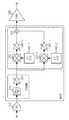
도 3은 본 발명의 실시 예에 따른 무선 송신 장치의 블록 구성을 도시한다. 상기 도 3은 2개의 신호 처리 경로를 포함하는 실시 예를 도시한다.3 is a block diagram of a wireless transmission apparatus according to an embodiment of the present invention. 3 illustrates an embodiment including two signal processing paths.
상기 도 3을 참고하면, 상기 무선 송신 장치는 DAC(Digital to Analog Convertor)(310), 필터(320), 기저대역 VGA(Variable-gain Amplifier)(330), 제1LO 체인(340-1), 제2LO 체인(340-2), 제1믹서(mixer)(350-1), 제2믹서(350-2), 제1RF VGA(360-1), 제2RF VGA(360-2), 합산기(370), PAM(Power Amplifier Module)(380)을 포함한다. 상기 필터(320) 및 상기 기저대역 VGA(330)은 '송신 아날로그 기저대역(TXABB: Transmit Analog BaseBand) 처리부'로 통칭될 수 있다. 또한, 상기 제1LO 체인(340-1), 상기 제2LO 체인(340-2), 상기 제1믹서(350-1), 상기 제2믹서(350-2), 상기 제1RF VGA(360-1), 상기 제2RF VGA(360-2), 상기 합산기(370)는 'RF 신호 처리부'로 통칭될 수 있다.Referring to FIG. 3, the wireless transmitter includes a digital to analog converter (DAC) 310, a
상기 DAC(310)는 디지털 신호를 아날로그 신호로 변환한다. 상기 도 3에 도시되지 아니하였으나, 송신 비트열을 부호화(endocing) 및 변조함으로써 상기 DAC(310)로 입력되는 신호를 생성하는 수단이 더 포함될 수 있다.The
상기 필터(320)는 상기 아날로그 신호에서 의도하지 아니한 주파수 성분을 제거한다. 예를 들어, 상기 필터(320)는 상기 아날로그 신호에 포함된 DAC 이미지(image) 신호를 제거할 수 있다. 상기 DAC 이미지는 상기 DAC(310)의 클럭(clock) 주파수의 배수의 주파수에서 발생하는 복사 신호를 의미한다. 상기 필터(320)는 SAW(Surface Acoustic Wave) 필터일 수 있다.The
상기 기저대역 VGA(330)는 상기 필터(320)에서 출력되는 신호의 이득을 제어한다. 상기 기저대역 VGA(330)에 의한 이득 제어는 신호 이득의 동적 범위의 일부를 확보하기 위한 것으로서, 상기 기저대역 VGA(330)는 상기 동적 범위 중 기저대역에서의 부담 부분을 처리한다. 다시 말해, 상기 기저대역 VGA(330)는 상기 제1믹서(350-1) 및 상기 제2믹서(350-2)로 입력되는 아날로그 신호의 크기를 조절한다.The
상기 제1LO 체인(340-1)은 상기 제1믹서(350-1)에서 RF 대역 신호를 생성하기 위해 필요한 고주파 신호를 생성하고, 상기 제2LO 체인(340-2)은 상기 제2믹서(350-2)에서 RF 대역 신호를 생성하기 위해 필요한 고주파 신호를 생성한다. 상기 제1LO 체인(340-1) 및 상기 제2LO 체인(340-2)은 PLL(Phase Locked Loop) 구조로 구성될 수 있다. 출력 레벨에 따른 동작 경로 선택에 따라, 상기 제1LO 체인(340-1) 및 상기 제2LO 체인(340-2) 중 하나는 오프 상태일 수 있다.The first LO chain 340-1 generates a high frequency signal necessary to generate an RF band signal in the first mixer 350-1, and the second LO chain 340-2 generates the second mixer 350. In (2), a high frequency signal necessary to generate an RF band signal is generated. The first LO chain 340-1 and the second LO chain 340-2 may be configured in a phase locked loop (PLL) structure. According to the operation path selection according to the output level, one of the first LO chain 340-1 and the second LO chain 340-2 may be in an off state.
상기 제1믹서(350-1)는 상기 제1LO 체인(340-1)로부터 제공되는 고주파 신호를 이용하여 상기 기저대역 VGA(330)로부터 제공되는 기저대역 신호를 RF 대역 신호로 상승 변환(up-conversion)한다. 상기 제2믹서(350-2)는 상기 제2LO 체인(340-2)로부터 제공되는 고주파 신호를 이용하여 상기 기저대역 VGA(330)로부터 제공되는 기저대역 신호를 RF 대역 신호로 상승 변환한다. 상기 제1믹서(350-1) 및 상기 제2믹서(350-2)는 상기 기저대역 VGA(330)의 출력 신호를 공유한다. 출력 레벨에 따른 동작 경로 선택에 따라, 상기 제1믹서(350-1) 및 상기 제2믹서(350-2) 중 하나는 오프 상태일 수 있다. 본 발명의 실시 예에 따르면, 각 신호 처리 경로마다 별개의 믹서를 포함함으로써, 상승 변환된 RF 대역 신호가 각 경로의 입력으로서 공유되지 아니한다. 즉, 상기 제1믹서(350-1) 및 상기 제2믹서(350-2)로 인해, 각 경로 내의 증폭기들(360-1 및 360-2)로 별개의 입력 신호들이 제공될 수 있다. 다시 말해, 상기 제1믹서(350-1) 및 상기 제2믹서(350-2)로 인해, 각 경로 내의 증폭기들(360-1 및 360-2)의 입력단에서 하나의 신호가 공유되지 아니할 수 있다.The first mixer 350-1 up-converts the baseband signal provided from the
상기 제1RF VGA(360-1)는 상기 제1믹서(350-1)에서 출력되는 RF 대역 신호의 이득을 제어한다. 상기 제2RF VGA(360-2)는 상기 제2믹서(350-2)에서 출력되는 RF 대역 신호의 이득을 제어한다. 본 발명의 실시 예에 따라, 상기 제1RF VGA(360-1) 및 상기 제2RF VGA(360-2)는 서로 다른 출력 레벨로 신호의 이득을 제어한다. 상기 제1RF VGA(360-1) 및 상기 제2RF VGA(360-2) 각각은 적어도 하나의 증폭 소자를 포함하여 구성된다. 예를 들어, 상기 증폭 소자는 트랜지스터를 포함할 수 있다. 예를 들어, 상기 제1RF VGA(360-1)가 상기 제2RF VGA(360-2)보다 더 큰 출력 레벨을 담당하는 경우, 상기 제1RF VGA(360-1)가 상기 제2RF VGA(360-2)보다 더 많은 개수의 출력 소자들을 포함하거나, 또는, 더 큰 크기의 출력 소자를 포함할 수 있다. 출력 레벨에 따른 동작 경로 선택에 따라, 상기 제1RF VGA(360-1) 및 상기 제2RF VGA(360-2) 중 하나는 오프 상태일 수 있다.The first RF VGA 360-1 controls the gain of the RF band signal output from the first mixer 350-1. The second RF VGA 360-2 controls the gain of the RF band signal output from the second mixer 350-2. According to an embodiment of the present invention, the first RF VGA 360-1 and the second RF VGA 360-2 control a gain of a signal at different output levels. Each of the first RF VGA 360-1 and the second RF VGA 360-2 includes at least one amplifier. For example, the amplifying device may include a transistor. For example, when the first RF VGA 360-1 is responsible for a greater output level than the second RF VGA 360-2, the first RF VGA 360-1 is the second RF VGA 360-360. It may include a larger number of output elements than 2), or may include a larger size output element. According to the operation path selection according to the output level, one of the first RF VGA 360-1 and the second RF VGA 360-2 may be in an off state.
상기 합산기(370)는 상기 제1RF VGA(360-1) 및 상기 제2RF VGA(360-2)로부터의 이득 제어된 신호들을 합산한다. 즉, 상기 제1RF VGA(360-1) 및 상기 제2RF VGA(360-2)가 동시에 동작할 수 있다. 상기 PAM(380)은 상기 합산기(370)를 통해 합산된 이득 제어된 신호들의 전력을 증폭한다.The
상기 도 3에 도시된 실시 예에서, 상기 제1LO 체인(340-1), 상기 제1믹서(350-1), 상기 제1RF VGA(360-1)가 제1경로를, 상기 제2LO 체인(340-2), 상기 제2믹서(350-2), 상기 제2RF VGA(360-2)가 제2경로를 구성한다. 상기 제1경로 및 상기 제2경로는 서로 다른 출력 레벨의 신호를 생성하며, 선택적으로 동작하거나, 또는, 동시에 동작할 수 있다. 예를 들어, 높은 출력 레벨이 필요한 경우, 상기 제1경로에 속하는 상기 제1LO 체인(340-1), 상기 제1믹서(350-1), 상기 제1RF VGA(360-1)가 동작하고, 상기 제2경로에 속하는 상기 제2LO 체인(340-2), 상기 제2믹서(350-2), 상기 제2RF VGA(360-2)는 오프 상태일 수 있다. 여기서, 상기 오프 상태는 각 모듈에 공급되는 전원이 차단되거나, 또는, 비활성 신호가 인가된 상태를 포함할 수 있다.In the example illustrated in FIG. 3, the first LO chain 340-1, the first mixer 350-1, and the first RF VGA 360-1 designate a first path and the second LO chain ( 340-2), the second mixer 350-2, and the second RF VGA 360-2 constitute a second path. The first path and the second path may generate signals of different output levels, selectively operate, or may operate simultaneously. For example, when a high output level is required, the first LO chain 340-1, the first mixer 350-1, and the first RF VGA 360-1 belonging to the first path operate. The second LO chain 340-2, the second mixer 350-2, and the second RF VGA 360-2 belonging to the second path may be in an off state. The off state may include a state in which power supplied to each module is cut off or an inactive signal is applied.
상기 도 3에 도시된 실시 예에서, 상기 제1LO 체인(340-1) 및 상기 제2LO 체인(340-2)은 동일한 성능을 가질 수 있다. 여기서, 상기 성능은 원하는 주파수 외 다른 주파수의 신호, 즉, 잡음의 크기를 나타내는 잡음 특성을 포함한다. 성능이 우수함은 잡음 특성이 양호함, 즉, 잡음의 크기가 작음을 의미한다. 이 경우, 상기 제1LO 체인(340-1) 및 상기 제2LO 체인(340-2)은 동일한 양의 전류를 소모한다.In the embodiment illustrated in FIG. 3, the first LO chain 340-1 and the second LO chain 340-2 may have the same performance. Here, the performance includes a noise characteristic representing a signal of a frequency other than the desired frequency, that is, the amount of noise. Good performance means that the noise characteristics are good, that is, the amount of noise is small. In this case, the first LO chain 340-1 and the second LO chain 340-2 consume the same amount of current.
본 발명의 다른 실시 예에 따라, 상기 제1LO 체인(340-1) 및 상기 제2LO 체인(340-2)은 서로 다른 잡음 특성을 가질 수 있다. 이득 제어 과정에서 잡음 또한 함께 증폭되므로, 상기 잡음 신호의 크기는 상기 제1LO 체인(340-1) 및 상기 제2LO 체인(340-2)이 속한 경로에 대응되는 출력 레벨이 클수록 최종 출력에 큰 영향을 미친다. 다시 말해, 출력 레벨이 작다면, 상기 잡음 신호에 의한 악영향이 상대적으로 적다. 그러므로, 작은 출력 레벨에 대응되는 경로에 속한다면, 상대적으로 잡음 특성이 열악한 LO 체인이 사용될 수 있으며, 이 경우, 전류 소비량이 감소한다. 예를 들어, 상기 제2경로가 상기 제1경로에 비해 작은 출력 레벨에 대응되는 경우, 상기 제2LO 체인(340-2)은 상기 제1LO 체인(340-1)에 비하여 열악한 잡음 특성을 가질 수 있다. 이에 따라, 상기 제2LO 체인(340-2)은 상기 제1LO 체인(340-1)에 비하여 적은 양의 전류 소비만으로 고주파 신호를 생성할 수 있다.According to another embodiment of the present disclosure, the first LO chain 340-1 and the second LO chain 340-2 may have different noise characteristics. Since the noise is also amplified in the gain control process, the magnitude of the noise signal has a greater effect on the final output as the output level corresponding to the path to which the first LO chain 340-1 and the second LO chain 340-2 belongs is larger. Crazy In other words, if the output level is small, the adverse effect of the noise signal is relatively small. Therefore, if it belongs to a path corresponding to a small output level, a relatively low noise LO chain can be used, in which case the current consumption is reduced. For example, when the second path corresponds to a smaller output level than the first path, the second LO chain 340-2 may have a lower noise characteristic than the first LO chain 340-1. have. Accordingly, the second LO chain 340-2 may generate a high frequency signal with only a small amount of current consumption compared to the first LO chain 340-1.
상기 도 3에 도시된 실시 예에서, 상기 제1경로는 상기 제1LO 체인(340-1)을 포함하고, 상기 제2경로는 상기 제2LO 체인(340-1)을 포함한다. 다시 말해, 각 경로를 위한 별도의 LO 체인이 존재한다. 그러나, 본 발명의 다른 실시 예에 따라, 상기 제1LO 체인(340-1) 및 상기 제2LO 체인(340-2)의 역할을 하나의 LO 체인이 수행할 수 있다. 다시 말해, 상기 제1경로 및 상기 제2경로 각각을 위한 복수의 LO 체인들이 아닌, 하나의 공통 LO 체인이 상기 제1믹서(350-1) 및 상기 제2믹서(350-1)로 고주파 신호를 제공할 수 있다. 이 경우, 상기 공통 LO 체인은 신호 이득 제어를 위해 선택된 경로와 무관하게 항상 동작할 수 있다.In the example illustrated in FIG. 3, the first path includes the first LO chain 340-1 and the second path includes the second LO chain 340-1. In other words, there is a separate LO chain for each path. However, according to another embodiment of the present invention, one LO chain may serve as the first LO chain 340-1 and the second LO chain 340-2. In other words, one common LO chain, rather than a plurality of LO chains for each of the first path and the second path, is a high frequency signal to the first mixer 350-1 and the second mixer 350-1. Can be provided. In this case, the common LO chain may always operate regardless of the path selected for signal gain control.
상기 도 3에 도시되지 아니하였으나, 목적한 출력 레벨에 따라, 상기 제1경로 및 상기 제2경로 중 동작할 적어도 하나의 경로를 결정하고, 결정된 경로가 동작하도록 제어하는 제어부가 더 포함될 수 있다. 예를 들어, 상기 제어부는 상기 결정된 경로를 활성화시키기 위한 신호를 생성할 수 있다. 또한, 상기 제어부는 상기 결정된 경로 외 나머지를 비활성화시키기 위한 신호를 생성할 수 있다.
Although not shown in FIG. 3, the controller may further include a controller configured to determine at least one path to operate among the first path and the second path and to control the determined path according to the desired output level. For example, the controller may generate a signal for activating the determined path. In addition, the controller may generate a signal for deactivating the rest other than the determined path.
도 4는 본 발명의 다른 실시 예에 따른 무선 송신 장치의 블록 구성을 도시한다. 상기 도 4는 N개의 신호 처리 경로를 포함하는 실시 예를 도시한다.4 is a block diagram of a wireless transmission apparatus according to another embodiment of the present invention. 4 illustrates an embodiment including N signal processing paths.
상기 도 4를 참고하면, 상기 무선 송신 장치는 DAC(410), 필터(420), 기저대역 VGA(430), N개의 LO 체인들(440-1 내지 440-N), N개의 믹서들(450-1 내지 450-N), N개의 RF VGA들(460-1 내지 460-N), 합산기(470), PAM(480)을 포함한다. 상기 필터(420) 및 상기 기저대역 VGA(430)은 '송신 아날로그 기저대역 처리부'로 통칭될 수 있다. 또한, 상기 N개의 LO 체인들(440-1 내지 440-N), 상기 N개의 믹서들(450-1 내지 450-N), 상기 N개의 RF VGA들(460-1 내지 460-N), 상기 합산기(470)는 'RF 신호 처리부'로 통칭될 수 있다.Referring to FIG. 4, the wireless transmission apparatus includes a
상기 DAC(410)는 디지털 신호를 아날로그 신호로 변환한다. 상기 도 4에 도시되지 아니하였으나, 송신 비트열을 부호화 및 변조함으로써 상기 DAC(410)로 입력되는 신호를 생성하는 수단이 더 포함될 수 있다.The
상기 필터(420)는 상기 아날로그 신호에서 의도하지 아니한 주파수 성분을 제거한다. 예를 들어, 상기 필터(420)는 상기 아날로그 신호에 포함된 DAC 이미지 신호를 제거할 수 있다. 상기 DAC 이미지는 상기 DAC(410)의 클럭 주파수의 배수의 주파수에서 발생하는 복사 신호를 의미한다. 상기 필터(420)는 SAW 필터일 수 있다.The
상기 기저대역 VGA(430)는 상기 필터(420)에서 출력되는 신호의 이득을 제어한다. 상기 기저대역 VGA(430)에 의한 이득 제어는 신호 이득의 동적 범위의 일부를 확보하기 위한 것으로서, 상기 기저대역 VGA(430)는 상기 동적 범위 중 기저대역에서의 부담 부분을 처리한다. 다시 말해, 상기 기저대역 VGA(430)는 상기 N개의 믹서들(450-1 내지 450-N)로 입력되는 아날로그 신호의 크기를 조절한다.The
상기 N개의 LO 체인들(440-1 내지 440-N)은 상기 N개의 믹서들(450-1 내지 450-N)에서 RF 대역 신호를 생성하기 위해 필요한 고주파 신호를 생성한다. 상기 도 4에 도시된 바와 같이, 상기 N개의 LO 체인들(440-1 내지 440-N) 및 상기 N개의 믹서들(450-1 내지 450-N)은 일대일 대응관계를 가질 수 있다. 상기 N개의 LO 체인들(440-1 내지 440-N)은 PLL 구조로 구성될 수 있다. 출력 레벨에 따른 동작 경로 선택에 따라, 상기 N개의 LO 체인들(440-1 내지 440-N) 중 일부는 오프 상태일 수 있다.The N LO chains 440-1 through 440 -N generate a high frequency signal necessary to generate an RF band signal in the N mixers 450-1 through 450 -N. As shown in FIG. 4, the N LO chains 440-1 to 440 -N and the N mixers 450-1 to 450 -N may have a one-to-one correspondence. The N LO chains 440-1 through 440 -N may be configured in a PLL structure. Depending on the operation path selection according to the output level, some of the N LO chains 440-1 through 440 -N may be in an off state.
상기 N개의 믹서들(450-1 내지 450-N) 각각은 상기 N개의 LO 체인들(440-1 내지 440-N) 각각으로부터 제공되는 고주파 신호를 이용하여 상기 기저대역 VGA(430)로부터 제공되는 기저대역 신호를 RF 대역 신호로 상승 변환한다. 상기 N개의 믹서들(450-1 내지 450-N)은 상기 기저대역 VGA(430)의 출력 신호를 공유한다. 출력 레벨에 따른 동작 경로 선택에 따라, 상기 N개의 믹서들(450-1 내지 450-N) 중 일부는 오프 상태일 수 있다. 본 발명의 실시 예에 따르면, 각 신호 처리 경로마다 별개의 믹서를 포함함으로써, 상승 변환된 RF 대역 신호가 각 경로의 입력으로서 공유되지 아니한다. 즉, 상기 N개의 믹서들(450-1 내지 450-N)로 인해, 각 경로 내의 증폭기들(460-1 내지 460-N)로 별개의 입력 신호들이 제공될 수 있다. 다시 말해, 상기 N개의 믹서들(450-1 내지 450-N)로 인해, 각 경로 내의 증폭기들(460-1 내지 460-N)의 입력단에서 하나의 신호가 공유되지 아니할 수 있다.Each of the N mixers 450-1 through 450 -N is provided from the
상기 N개의 RF VGA들(460-1 내지 460-N) 각각은 상기 N개의 믹서들(450-1 내지 450-N) 각각에서 출력되는 RF 대역 신호의 이득을 제어한다. 본 발명의 실시 예에 따라, 상기 N개의 RF VGA들(460-1 내지 460-N)은 서로 다른 출력 레벨로 신호의 이득을 제어한다. 상기 N개의 RF VGA들(460-1 내지 460-N) 각각은 적어도 하나의 증폭 소자를 포함하여 구성된다. 예를 들어, 상기 증폭 소자는 트랜지스터를 포함할 수 있다. 예를 들어, 상기 제1RF VGA(460-1)가 상기 제N-RF VGA(460-N)보다 더 큰 출력 레벨을 담당하는 경우, 상기 제1RF VGA(460-1)가 상기 제N-RF VGA(460-N)보다 더 많은 개수의 출력 소자들을 포함하거나, 또는, 더 큰 크기의 출력 소자를 포함할 수 있다. 출력 레벨에 따른 동작 경로 선택에 따라, 상기 N개의 RF VGA들(460-1 내지 460-N) 중 일부는 오프 상태일 수 있다.Each of the N RF VGAs 460-1 through 460 -N controls a gain of an RF band signal output from each of the N mixers 450-1 through 450 -N. According to an embodiment of the present invention, the N RF VGAs 460-1 through 460 -N control a gain of a signal at different output levels. Each of the N RF VGAs 460-1 through 460 -N includes at least one amplifier. For example, the amplifying device may include a transistor. For example, when the first RF VGA 460-1 is responsible for a greater output level than the N-RF VGA 460-N, the first RF VGA 460-1 is the N-RF. It may include a larger number of output elements than the VGA 460 -N, or may include a larger sized output element. According to the operation path selection according to the output level, some of the N RF VGAs 460-1 through 460 -N may be in an off state.
상기 합산기(470)는 상기 N개의 RF VGA들(460-1 내지 460-N)로부터의 이득 제어된 신호들을 합산한다. 즉, 상기 N개의 RF VGA들(460-1 내지 460-N) 전부 또는 일부는 동시에 동작할 수 있다. 상기 PAM(480)은 상기 합산기(470)를 통해 합산된 이득 제어된 신호들의 전력을 증폭한다.The
상기 도 4에 도시된 실시 예에서, N개의 경로들이 구성된다. 상기 N개의 경로들은 서로 다른 출력 레벨의 신호를 생성하며, 선택적으로 동작하거나, 또는, 동시에 동작할 수 있다. 예를 들어, 높은 출력 레벨이 필요한 경우, 상기 제1경로에 속하는 모듈들이 동작하고, 나머지 경로에 속하는 모듈들은 오프 상태일 수 있다. 또는, 둘 이상의 일부 경로들에 속하는 모듈들이 동작하고, 나머지 경로에 속하는 모듈들은 오프 상태일 수 있다. 여기서, 상기 오프 상태는 각 모듈에 공급되는 전원이 차단되거나, 또는, 비활성 신호가 인가된 상태를 포함할 수 있다.In the embodiment shown in FIG. 4, N paths are configured. The N paths generate signals of different output levels and may be selectively operated or simultaneously operated. For example, when a high output level is required, modules belonging to the first path may operate and modules belonging to the remaining path may be off. Alternatively, modules belonging to two or more partial paths may operate, and modules belonging to the remaining paths may be off. The off state may include a state in which power supplied to each module is cut off or an inactive signal is applied.
상기 도 4에 도시된 실시 예에서, 상기 N개의 LO 체인들(440-1 내지 440-N) 은 동일한 성능을 가질 수 있다. 여기서, 상기 성능은 원하는 주파수 외 다른 주파수의 신호, 즉, 잡음의 크기를 나타내는 잡음 특성을 포함한다. 성능이 우수함은 잡음 특성이 양호함, 즉, 잡음의 크기가 작음을 의미한다. 이 경우, 상기 N개의 LO 체인들(440-1 내지 440-N)은 동일한 양의 전류를 소모한다.In the embodiment illustrated in FIG. 4, the N LO chains 440-1 through 440 -N may have the same performance. Here, the performance includes a noise characteristic representing a signal of a frequency other than the desired frequency, that is, the amount of noise. Good performance means that the noise characteristics are good, that is, the amount of noise is small. In this case, the N LO chains 440-1 through 440 -N consume the same amount of current.
본 발명의 다른 실시 예에 따라, 상기 N개의 LO 체인들(440-1 내지 440-N)은 서로 다른 잡음 특성을 가질 수 있다. 상기 잡음 신호의 크기는 출력 레벨이 클수록 최종 출력에 큰 영향을 미친다. 다시 말해, 출력 레벨이 작다면, 상기 잡음 신호에 의한 악영향이 상대적으로 적다. 그러므로, 작은 출력 레벨에 대응되는 경로에 속한다면, 상대적으로 잡음 특성이 열악한 LO 체인이 사용될 수 있으며, 이 경우, 전류 소비량이 감소한다.According to another embodiment of the present invention, the N LO chains 440-1 to 440 -N may have different noise characteristics. The magnitude of the noise signal has a greater effect on the final output as the output level is larger. In other words, if the output level is small, the adverse effect of the noise signal is relatively small. Therefore, if it belongs to a path corresponding to a small output level, a relatively low noise LO chain can be used, in which case the current consumption is reduced.
상기 N개의 LO 체인들(440-1 내지 440-N)간 서로 다른 잡음 특성을 가질 수 있는 경우, 상기 N개의 경로들은 출력 레벨 및 전류 소모량의 조합을 기준으로 구분될 수 있다. 즉, 출력 레벨이 동일한 복수의 경로들이 존재할 수 있으나, 출력 레벨이 동일한 복수의 경로들은 서로 다른 전류 소모량으로 동작 가능할 수 있다. 또한, 전류 소모량이 동일한 복수의 경로들이 존재할 수 있으나, 전류 소모량이 동일한 복수의 경로들은 서로 다른 출력 레벨을 가질 수 있다.When the N LO chains 440-1 to 440 -N may have different noise characteristics, the N paths may be classified based on a combination of output level and current consumption. That is, a plurality of paths having the same output level may exist, but a plurality of paths having the same output level may be operated at different current consumptions. In addition, a plurality of paths having the same current consumption may exist, but a plurality of paths having the same current consumption may have different output levels.
상기 도 4에 도시된 실시 예에서, 각 경로를 위한 별도의 LO 체인이 존재한다. 그러나, 본 발명의 다른 실시 예에 따라, 상기 N개의 LO 체인들(440-1 내지 440-N)의 역할을 하나의 LO 체인이 수행할 수 있다. 또는, 상기 N개의 LO 체인들(440-1 내지 440-N) 중 일부의 역할을 하나의 LO 체인이 수행할 수 있다.In the embodiment shown in FIG. 4 above, there is a separate LO chain for each path. However, according to another embodiment of the present invention, one LO chain may serve as the N LO chains 440-1 to 440 -N. Alternatively, one LO chain may perform a part of the N LO chains 440-1 to 440 -N.
상기 도 4에 도시되지 아니하였으나, 목적한 출력 레벨에 따라, N개의 경로들 중 동작할 적어도 하나의 경로를 결정하고, 결정된 경로가 동작하도록 제어하는 제어부가 더 포함될 수 있다. 예를 들어, 상기 제어부는 상기 결정된 경로를 활성화시키기 위한 신호를 생성할 수 있다. 또한, 상기 제어부는 상기 결정된 경로 외 나머지를 비활성화시키기 위한 신호를 생성할 수 있다.
Although not shown in FIG. 4, the controller may further include a controller configured to determine at least one path to operate among N paths and to control the determined path to operate according to a desired output level. For example, the controller may generate a signal for activating the determined path. In addition, the controller may generate a signal for deactivating the rest other than the determined path.
도 5는 본 발명의 실시 예에 따른 무선 송신 장치의 동작 절차를 도시한다.5 is a flowchart illustrating an operation of a wireless transmission apparatus according to an embodiment of the present invention.
상기 도 5를 참고하면, 상기 무선 송신 장치는 501단계에서, 제1출력 레벨이 필요한 경우, 제1믹서 및 제1증폭기를 포함하는 제1경로를 이용하여 RF 신호의 이득을 제어한다. 즉, 상기 무선 송신 장치는 RF 신호의 이득을 제어하기 위한 복수의 경로들을 포함하며, 상기 경로들은 다른 경로와 독립적인 믹서 및 증폭기를 포함한다. 다시 말해, 상기 경로들은 각 믹서의 입력단에서 기저대역 신호를 공유할 수 있다.Referring to FIG. 5, in
이후, 상기 무선 송신 장치는 503단계로 진행하여, 제2출력 레벨이 필요한 경우, 제2믹서 및 제2증폭기를 포함하는 제2경로를 이용하여 RF 신호의 이득을 제어한다. RF 대역의 신호를 생성하기 위해, 상기 무선 송신 장치는 상기 제2믹서로 고주파 신호를 제공한다. 이를 위해, 상기 무선 송신 장치는 상기 제1믹서로 고주파 신호를 제공하는 LO 체인을 재사용하거나, 또는, 상기 제2믹서로 고주파 신호를 제공하기 위한 별도의 LO 체인을 구비할 수 있다. 상기 제2믹서로 고주파 신호를 제공하기 위한 별도의 LO 체인이 구비된 경우, 상기 별도의 LO 체인은 상기 제1믹서로 고주파 신호를 제공하기 위한 LO 체인과 상이한 잡음 특성을 가질 수 있다.In
이후, 상기 도 5에 도시되지 아니하였으나, 상기 무선 송신 장치는 이득 제어된 신호의 전력을 증폭한 후, 안테나를 통해 송신할 수 있다.
Subsequently, although not shown in FIG. 5, the wireless transmission device may amplify the power of the gain-controlled signal and then transmit it through the antenna.
도 6은 본 발명의 다른 실시 예에 따른 무선 송신 장치의 동작 절차를 도시한다.6 is a flowchart illustrating an operation procedure of a wireless transmission apparatus according to another embodiment of the present invention.
상기 도 6을 참고하면, 상기 무선 송신 장치는 601단계에서 출력 레벨에 대응하는 RF 이득 제어 경로를 결정한다. 즉, 상기 무선 송신 장치는 RF 신호의 이득을 제어하기 위한 복수의 경로들을 포함하며, 상기 경로들은 다른 경로와 독립적인 믹서 및 증폭기를 포함한다. 예를 들어, 상기 무선 송신 장치는 출력 레벨 및 RF 이득 제어 경로 간 대응 관계를 정의하는 정보를 저장할 수 있으며, 상기 정보에 기초하여 결정된 출력 레벨에 대응하는 경로를 선택할 수 있다.Referring to FIG. 6, in
이어, 상기 무선 송신 장치는 603단계로 진행하여 결정된 경로를 활성화시키기 위한 신호를 생성한다. 즉, 상기 무선 송신 장치는 구비된 복수의 경로들의 활성/비활성을 제어하는 제어부를 포함할 수 있으며, 상기 제어부를 통해 상기 결정된 경로를 활성화시키기 위한 신호를 생성할 수 있다. 이때, 상기 도 6에 도시되지 아니하였으나, 상기 무선 송신 장치는 상기 결정된 경로 외 나머지를 비활성화시키기 위한 신호를 더 생성할 수 있다.In
상기 도 6에 도시된 실시 예에서, 상기 무선 송신 장치는 출력 레벨에 기초하여 신호 이득을 제어할 경로를 결정한다. 본 발명의 다른 실시 예에 따라, 상기 무선 송신 장치는 전류 소모량에 기초하여 신호 이득을 제어할 경로를 결정할 수 있다. 또는, 상기 무선 송신 장치는 상기 출력 레벨 및 상기 전류 소모량에 기초하여 신호 이득을 제어할 경로를 결정할 수 있다.
In the embodiment shown in FIG. 6, the wireless transmission apparatus determines a path to control a signal gain based on an output level. According to another embodiment of the present disclosure, the wireless transmission apparatus may determine a path for controlling the signal gain based on the current consumption amount. Alternatively, the wireless transmission apparatus may determine a path to control a signal gain based on the output level and the current consumption amount.
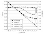
도 7은 본 발명의 실시 예에 따른 무선 송신 장치의 성능 그래프를 도시한다. 상기 도 7에서, 가로축은 이득 제어 코드(control code)를, 좌측의 세로축은 이득을, 우측의 세로축은 이득 단계를 나타낸다. 상기 이득 제어 코드는 6dB 간격의 일정한 이득 단계에 대응하도록 정의된다.7 illustrates a performance graph of a wireless transmission apparatus according to an embodiment of the present invention. In FIG. 7, the horizontal axis represents a gain control code, the left vertical axis represents gain, and the right vertical axis represents gain stage. The gain control code is defined to correspond to a constant gain step of 6 dB intervals.
상기 이득 제어 코드가 증가할수록 작은 출력이 얻어지는 것이 바람직하다. 그러나, 상기 도 7에 나타난 바와 같이, 종래 기술의 경우, 작은 출력으로 갈수록 이득 단계의 크기가 일정하게 유지되지 아니하고, 점차 감소한다. 이는, 턴-오프된 증폭 소자들을 통한 누설 신호에 의해, 최종 출력의 크기가 원하는 레벨에 대비하여 증가하기 때문이다. 하지만, 본원발명의 경우, 이득 단계의 크기가 종래 기술에 비하여 일정하게 유지되며, 이에 따라, 작은 출력 레벨의 최종 출력이 생성될 수 있다.
It is desirable that as the gain control code increases, smaller outputs are obtained. However, as shown in FIG. 7, in the prior art, the magnitude of the gain stage does not remain constant, but gradually decreases, toward the smaller output. This is because, with the leakage signal through the turn-off amplification elements, the magnitude of the final output increases relative to the desired level. However, in the present invention, the size of the gain stage is kept constant compared to the prior art, so that a final output of a small output level can be produced.
상술한 본 발명의 다양한 실시 예들에 따른 RFIC 구조를 통해 얻을 수 있는 장점은 누설 신호의 최소화를 통한 동적 범위의 확보 및 동작 전류의 감소를 포함할 수 있다.Advantages obtained through the RFIC structure according to various embodiments of the present disclosure described above may include securing dynamic range and reducing operating current through minimization of a leakage signal.
상기 누설 신호의 측면을 살펴보면, 믹서에서 경로가 나누어지므로 각 경로 내의 증폭기들에 별개의 입력이 인가된다. 저이득 모드를 위한 경로에서의 증폭기가 작은 출력을 위해 최적화되므로, 병렬로 연결된 증폭 소자들의 크기가 종래 기술에 비하 작아고, 이에 따라, 기생 성분이 감소한다. 또한, 믹서 역시 상기 저이득 모드에 적합하도록 작은 크기의 트랜지스터로 구성될 수 있으므로, 상기 믹서 자체에서 발생할 수 있는 LO 신호의 누설도 감소한다. 따라서, 상기 종래 기술의 경우에 비하여, 동적 범위 확보가 용이하게 하고, 이특 제어에 발생할 수 있는 오류가 감소한다.Looking at the side of the leakage signal, since the path is divided in the mixer, a separate input is applied to the amplifiers in each path. Since the amplifiers in the path for the low gain mode are optimized for small outputs, the size of the amplifying elements connected in parallel is smaller than in the prior art, thus reducing parasitic components. In addition, the mixer may also be composed of transistors of small size to fit the low gain mode, thereby reducing the leakage of the LO signal that may occur in the mixer itself. Therefore, as compared with the conventional technique, it is easy to secure the dynamic range and the error that can occur in heterogeneous control is reduced.
상기 전류 소모의 관점에서 살펴보면, 출력 레벨에 따라 증폭기에서 소모되는 전류 량이 달라지므로, 종래 기술보다 더 많은 전류가 소모되지는 아니한다. 추가적으로, 저이득 모드의 경우 동작하는 믹서, LO 체인이 고이득 모드를 위한 경로와 다르게 구성될 수 있다. 즉, 상기 믹서 및 상기 LO 체인이 상기 저이득 모드에 적합하게 상대적으로 작은 셀(cell)로 구성된다면, 고이득 모드에 비하여 더 적은 전류가 소비될 수 있다.In view of the current consumption, since the amount of current consumed in the amplifier varies depending on the output level, more current is not consumed than in the prior art. In addition, in the case of the low gain mode, the mixer and the LO chain operating may be configured differently from the path for the high gain mode. That is, if the mixer and the LO chain consist of relatively small cells suitable for the low gain mode, less current may be consumed compared to the high gain mode.
특히, 상기 LO 체인의 경우, 송신 잡음의 요구 조건에 민감하게 설계되는 것이 일반적이다. 통신 규격에 따르면, 수신 주파수 대역에서 나타나는 잡음의 절대값이 LO 체인 설계의 지표가 될 수 있다. 상기 요구 조건은 송신 신호가 큰 출력을 가질 때 민감한 경향을 가지며, 작은 출력 시에는 충분한 마진(margin)을 가진다. 상기 LO 체인의 저잡음 설계를 위해 더 많은 전류 소모가 요구되며, 따라서, 저이득 모드에서의 LO 체인은 잡음 특성보다 저전력을 고려하여 설계될 수 있다. 상술한 바와 같은 모드 별 회로 구성이 가능해지므로, 본 발명의 다양한 실시 예들은 RFIC의 전류소모 감소 효과를 제공할 수 있다.In particular, the LO chain is generally designed to be sensitive to the requirements of the transmission noise. According to the communication standard, the absolute value of noise appearing in the reception frequency band may be an indicator of the LO chain design. The requirement tends to be sensitive when the transmitted signal has a large output and has a sufficient margin at a small output. More current consumption is required for the low noise design of the LO chain, and therefore, the LO chain in the low gain mode can be designed considering lower power than noise characteristics. As the circuit configuration for each mode as described above becomes possible, various embodiments of the present invention can provide a current consumption reduction effect of the RFIC.
또한, 본 발명의 다양한 실시 예들에 따르면, 송신 장치는 같은 출력 레벨에 대해 고성능 모드 및 저전력 소비 모드로 구분되는 구조로 설계되고, 필요에 따라 선택적으로 동작함으로써, 고성능이 필요하지 아니하는 경우에 추가적인 전류 소모를 줄일 수 있다.
In addition, according to various embodiments of the present disclosure, the transmission device is designed in a structure divided into a high performance mode and a low power consumption mode for the same output level, and selectively operates as needed, so that additional performance is not required when high performance is not required. Current consumption can be reduced.
본 발명의 청구항 또는 명세서에 기재된 실시 예들에 따른 방법들은 하드웨어, 소프트웨어, 또는 하드웨어와 소프트웨어의 조합의 형태로 구현될(implemented) 수 있다.Methods according to the embodiments described in the claims or the specification of the present invention may be implemented in the form of hardware, software, or a combination of hardware and software.
소프트웨어로 구현하는 경우, 하나 이상의 프로그램(소프트웨어 모듈)을 저장하는 컴퓨터 판독 가능 저장 매체가 제공될 수 있다. 컴퓨터 판독 가능 저장 매체에 저장되는 하나 이상의 프로그램은, 전자 장치(device) 내의 하나 이상의 프로세서에 의해 실행 가능하도록 구성된다(configured for execution). 하나 이상의 프로그램은, 전자 장치로 하여금 본 발명의 청구항 또는 명세서에 기재된 실시 예들에 따른 방법들을 실행하게 하는 명령어(instructions)를 포함한다.When implemented in software, a computer-readable storage medium for storing one or more programs (software modules) may be provided. One or more programs stored in a computer readable storage medium are configured for execution by one or more processors in an electronic device. One or more programs include instructions that cause an electronic device to execute methods in accordance with embodiments described in the claims or specifications of the present invention.
이러한 프로그램(소프트웨어 모듈, 소프트웨어)은 랜덤 액세스 메모리 (random access memory), 플래시(flash) 메모리를 포함하는 불휘발성(non-volatile) 메모리, 롬(ROM: Read Only Memory), 전기적 삭제가능 프로그램가능 롬(EEPROM: Electrically Erasable Programmable Read Only Memory), 자기 디스크 저장 장치(magnetic disc storage device), 컴팩트 디스크 롬(CD-ROM: Compact Disc-ROM), 디지털 다목적 디스크(DVDs: Digital Versatile Discs) 또는 다른 형태의 광학 저장 장치, 마그네틱 카세트(magnetic cassette)에 저장될 수 있다. 또는, 이들의 일부 또는 전부의 조합으로 구성된 메모리에 저장될 수 있다. 또한, 각각의 구성 메모리는 다수 개 포함될 수도 있다.Such programs (software modules, software) may include random access memory, non-volatile memory including flash memory, Read Only Memory (ROM), and electrically erasable programmable ROM. (EEPROM: Electrically Erasable Programmable Read Only Memory), magnetic disc storage device, compact disc ROM (CD-ROM), digital versatile discs (DVDs) or other forms It can be stored in an optical storage device, a magnetic cassette. Or, it may be stored in a memory composed of some or all of these combinations. In addition, each configuration memory may be included in plural.
또한, 상기 프로그램은 인터넷(Internet), 인트라넷(Intranet), LAN(Local Area Network), WLAN(Wide LAN), 또는 SAN(Storage Area Network)과 같은 통신 네트워크, 또는 이들의 조합으로 구성된 통신 네트워크를 통하여 접근(access)할 수 있는 부착 가능한(attachable) 저장 장치(storage device)에 저장될 수 있다. 이러한 저장 장치는 외부 포트를 통하여 본 발명의 실시 예를 수행하는 장치에 접속할 수 있다. 또한, 통신 네트워크상의 별도의 저장장치가 본 발명의 실시 예를 수행하는 장치에 접속할 수도 있다.
In addition, the program may be implemented through a communication network such as the Internet, an intranet, a local area network (LAN), a wide area network (WLAN), or a storage area network (SAN), or a combination thereof. It may be stored in an attachable storage device that is accessible. Such a storage device may be connected to a device for performing an embodiment of the present invention through an external port. In addition, a separate storage device on a communication network may be connected to a device for performing an embodiment of the present invention.
상술한 본 발명의 구체적인 실시 예들에서, 발명에 포함되는 구성 요소는 제시된 구체적인 실시 예에 따라 단수 또는 복수로 표현되었다. 그러나, 단수 또는 복수의 표현은 설명의 편의를 위해 제시한 상황에 적합하게 선택된 것으로서, 본 발명이 단수 또는 복수의 구성 요소에 제한되는 것은 아니며, 복수로 표현된 구성 요소라하더라도 단수로 구성되거나, 단수로 표현된 구성 요소라 하더라도 복수로 구성될 수 있다.In specific embodiments of the present invention described above, components included in the invention are expressed in the singular or plural number according to the specific embodiments presented. However, the singular or plural expressions are selected to suit the situations presented for convenience of description, and the present invention is not limited to the singular or plural elements, and the singular or plural elements may be singular or singular. Even expressed components may be composed of a plurality.
한편 본 발명의 상세한 설명에서는 구체적인 실시 예에 관해 설명하였으나, 본 발명의 범위에서 벗어나지 않는 한도 내에서 여러 가지 변형이 가능함은 물론이다. 그러므로 본 발명의 범위는 설명된 실시 예에 국한되어 정해져서는 아니 되며 후술하는 특허청구의 범위뿐만 아니라 이 특허청구의 범위와 균등한 것들에 의해 정해져야 한다.Meanwhile, in the detailed description of the present invention, specific embodiments have been described, but various modifications are possible without departing from the scope of the present invention. Therefore, the scope of the present invention should not be limited to the described embodiments, but should be defined not only by the scope of the following claims, but also by those equivalent to the scope of the claims.
Claims (22)
Translated fromKorean기저대역 신호를 제공하는 기저대역 프로세서와,
복수의 믹서(mixer)들, 복수의 증폭기들, 및 복수의 LO들(local oscillators)을 포함하는 RF(radio frequency) 프로세서와, 상기 복수의 LO들은 제1 임계값보다 큰 이득을 위한 제1 LO와 제2 임계값보다 작은 이득을 위한 제2 LO를 포함하고,
상기 RF 프로세서와 동작적으로 결합되는 안테나와,
상기 무선 송신 장치의 요구되는 이득이 상기 제1 임계값보다 크고 상기 제2 임계값보다 작은 경우, 복수의 신호 경로들 중에서 제1 신호 경로 및 제2 신호 경로를 식별하고,
상기 무선 송신 장치의 동작 모드가 고성능 모드(high performance mode)인 경우, 상기 제1 신호 경로 및 상기 제2 신호 경로 중에서 상기 제1 신호 경로를 통신 경로로 식별하고,
상기 무선 송신 장치의 동작 모드가 저전력 소비 모드(low power consumption mode)인 경우, 상기 제1 신호 경로 및 상기 제2 신호 경로 중에서 상기 제1 신호 경로를 상기 통신 경로로 식별하도록 구성되는 제어기(controller)를 포함하고,
상기 복수의 신호 경로들 각각은, 상기 복수의 믹서들 중에서 하나, 상기 복수의 증폭기들 중에서 하나 , 상기 복수의 LO들 중에서 하나를 포함하고,
상기 안테나는, 상기 기저대역 신호로부터 상기 식별된 통신 경로를 이용하여 생성된 출력 신호를 전송하도록 구성되고,
상기 제1 신호 경로는 상기 요구되는 이득에 대응하고, 상기 제1 신호 경로의 상기 제1 LO는 제1 전류량(current quantity)을 소모하도록 구성되고,
상기 제2 신호 경로는 상기 요구되는 이득에 대응하고, 상기 제2 신호 경로의 상기 제2 LO는 상기 제1 전류량보다 적은 제2 전류량을 소모하도록 구성되는 장치.
In the radio transmitting apparatus,
A baseband processor providing a baseband signal,
A radio frequency (RF) processor comprising a plurality of mixers, a plurality of amplifiers, and a plurality of local oscillators, wherein the plurality of LOs are first LOs for gain greater than a first threshold; And a second LO for a gain less than a second threshold,
An antenna operatively coupled to the RF processor;
When the required gain of the radio transmitting apparatus is greater than the first threshold and less than the second threshold, identifying a first signal path and a second signal path among a plurality of signal paths,
When the operation mode of the radio transmitting apparatus is a high performance mode, the first signal path is identified as a communication path among the first signal path and the second signal path,
A controller configured to identify the first signal path as the communication path among the first signal path and the second signal path when the operation mode of the radio transmitting apparatus is a low power consumption mode. Including,
Each of the plurality of signal paths comprises one of the plurality of mixers, one of the plurality of amplifiers, one of the plurality of LOs,
The antenna is configured to transmit an output signal generated using the identified communication path from the baseband signal,
The first signal path corresponds to the desired gain, the first LO of the first signal path is configured to consume a first current quantity,
The second signal path corresponds to the desired gain, and wherein the second LO of the second signal path is configured to consume a second amount of current less than the first amount of current.
상기 복수의 믹서들 각각은, 상기 복수의 LO들 각각으로부터 제공되는 주파수를 이용하여, 상기 기저대역 신호를 상향-변환(up-converting)함으로써, RF(radio frequency) 신호를 생성하도록 구성되고,
상기 복수의 증폭기들 각각은, 상기 RF 신호를 증폭하도록 구성되는 장치.
The method of claim 1,
Each of the plurality of mixers is configured to generate a radio frequency (RF) signal by up-converting the baseband signal using a frequency provided from each of the plurality of LOs,
Each of the plurality of amplifiers is configured to amplify the RF signal.
상기 복수의 증폭기들은, 다른 이득을 제공하기 위해 서로 다른 개수의 증폭 소자들을 포함하는 증폭기들을 포함하는 장치.
The method of claim 1,
Wherein the plurality of amplifiers comprises amplifiers comprising different numbers of amplifying elements to provide different gains.
상기 복수의 증폭기들은, 다른 이득을 제공하기 위해, 서로 다른 크기의 증폭 소자들을 포함하는 증폭기들을 포함하는 장치.
The method of claim 1,
Wherein the plurality of amplifiers comprise amplifiers comprising amplifying elements of different sizes to provide different gains.
상기 제2 신호 경로의 상기 제2 LO의 크기는, 상기 제1 신호 경로의 상기 제1 LO의 크기보다 작은 장치
The method of claim 1,
The magnitude of the second LO of the second signal path is less than the magnitude of the first LO of the first signal path
2. The first amount of current according to claim 1, wherein the first amount of current is smaller than the second amount of noise associated with the second LO for the low power consumption mode so that the first noise level for the first LO for the high performance mode is smaller. Device larger than the amount of current.
상기 무선 송신 장치의 요구되는 이득이 제1 임계값보다 크고 제2 임계값보다 작은 경우, 복수의 신호 경로들 중에서 제1 신호 경로 및 제2 신호 경로를 식별하는 과정과,
상기 무선 송신 장치의 동작 모드가 고성능 모드(high performance mode)인 경우, 상기 제1 신호 경로 및 상기 제2 신호 경로 중에서 상기 제1 신호 경로를 통신 경로로 식별하는 과정과,
상기 무선 송신 장치의 동작 모드가 저전력 소비 모드(low power consumption mode)인 경우, 상기 제1 신호 경로 및 상기 제2 신호 경로 중에서 상기 제1 신호 경로를 상기 통신 경로로 식별하는 과정과, 상기 복수의 신호 경로들 각각은, 복수의 믹서들(mixers) 중에서 하나, 복수의 증폭기들 중에서 하나, 복수의 LO들(local oscillators) 중에서 하나를 포함하고,
기저대역 프로세서로부터 제공된 기저대역 신호로부터, 상기 식별된 경로를 이용하여, 출력 신호를 생성하는 과정과,
상기 복수의 증폭기들 각각과 결합된 안테나를 이용하여, 상기 출력 신호를 전송하는 과정을 포함하고,
상기 복수의 LO들은 제1 임계값보다 큰 이득을 위한 제1 LO와 제2 임계값보다 작은 이득을 위한 제2 LO를 포함하고
상기 제1 신호 경로는 상기 요구되는 이득에 대응하고, 상기 제1 신호 경로의 상기 제1 LO는 제1 전류량(current quantity)을 소모하고, 상기 제2 신호 경로는 상기 요구되는 이득에 대응하고, 상기 제2 신호 경로의 상기 제2 LO는 상기 제1 전류량보다 적은 제2 전류량을 소모하는 방법.
In the operation method of the radio transmitting apparatus,
Identifying a first signal path and a second signal path among a plurality of signal paths when the required gain of the radio transmitting apparatus is greater than a first threshold and less than a second threshold;
Identifying the first signal path as a communication path among the first signal path and the second signal path when the operation mode of the radio transmitting apparatus is a high performance mode;
Identifying the first signal path as the communication path among the first signal path and the second signal path when the operation mode of the wireless transmission apparatus is a low power consumption mode; Each of the signal paths comprises one of a plurality of mixers, one of a plurality of amplifiers, one of a plurality of local oscillators,
Generating an output signal from the baseband signal provided from the baseband processor using the identified path,
Transmitting the output signal using an antenna coupled to each of the plurality of amplifiers,
The plurality of LOs includes a first LO for gain greater than a first threshold and a second LO for gain less than a second threshold;
The first signal path corresponds to the desired gain, the first LO of the first signal path consumes a first current quantity, the second signal path corresponds to the required gain, And the second LO of the second signal path consumes a second amount of current less than the first amount of current.
상기 제1 신호 경로 및 상기 제2 신호 경로 각각은, 상기 요구되는 이득에 대응하고,
상기 통신 경로는, 상기 복수의 신호 경로들 중에서, 상기 복수의 신호 경로들에 대응하는 복수의 이득들에 관한 정보, 상기 요구되는 이득, 및 상기 고성능 모드 또는 상기 저전력 소비 모드 중 하나인 상기 무선 송신 장치의 동작 모드에 기반하여 식별되는 방법.
The method of claim 12,
Each of the first signal path and the second signal path corresponds to the desired gain,
Wherein said communication path is one of said plurality of signal paths, said information about a plurality of gains corresponding to said plurality of signal paths, said desired gain, and said high performance mode or said low power consumption mode. Method identified based on the mode of operation of the device.
상기 식별된 통신 경로를 활성화시키기 위한 신호를 생성하는 과정과,
상기 복수의 신호 경로들 중에서 상기 식별된 경로 외 다른 경로들 각각을 비활성화 시키는 신호를 생성하는 과정을 더 포함하는 방법.
The method of claim 12,
Generating a signal for activating the identified communication path;
Generating a signal to deactivate each of the other paths other than the identified path among the plurality of signal paths.
상기 복수의 신호 경로들에 대응하는 복수의 이득들에 관한 정보를 저장하도록 구성되는 저장소를 더 포함하고,
상기 제1 신호 경로 및 상기 제2 신호 경로 각각은, 상기 요구되는 이득에 대응하고,
상기 통신 경로는, 상기 복수의 신호 경로들 중에서 상기 정보, 상기 요구되는 이득, 및 상기 고성능 모드 또는 상기 저전력 소비 모드 중 하나인 상기 무선 송신 장치의 동작 모드에 기반하여 식별되는 장치.
The method of claim 1,
Further comprising a storage configured to store information regarding a plurality of gains corresponding to the plurality of signal paths,
Each of the first signal path and the second signal path corresponds to the desired gain,
And the communication path is identified based on the information, the desired gain, and an operating mode of the wireless transmitting device, one of the high performance mode or the low power consumption mode, among the plurality of signal paths.
상기 식별된 통신 경로를 활성화시키기 위한 신호를 생성하고,
상기 복수의 신호 경로들 중에서 상기 식별된 경로 외 다른 경로들 각각을 비활성화 시키는 신호를 생성하도록 추가적으로 구성되는 장치.
The method of claim 1, wherein the controller,
Generate a signal to activate the identified communication path,
And generate a signal to deactivate each of the other paths other than the identified path among the plurality of signal paths.
상기 복수의 LO들 각각으로부터 제공되는 주파수를 이용하여, 상기 기저대역 신호를 상향-변환(up-converting)함으로써, RF(radio frequency) 신호를 생성하는 과정과;
상기 RF 신호를 증폭하는 과정을 더 포함하는 방법.
The method of claim 12,
Generating a radio frequency (RF) signal by up-converting the baseband signal using a frequency provided from each of the plurality of LOs;
Amplifying the RF signal.
상기 복수의 증폭기들은, 다른 이득을 제공하기 위해 서로 다른 개수의 증폭 소자들을 포함하는 증폭기들을 포함하는 방법.
The method of claim 12,
Wherein the plurality of amplifiers comprises amplifiers comprising different numbers of amplifying elements to provide different gains.
상기 복수의 증폭기들은, 다른 이득을 제공하기 위해, 서로 다른 크기의 증폭 소자들을 포함하는 증폭기들을 포함하는 방법.
The method of claim 12,
Wherein the plurality of amplifiers comprises amplifiers comprising amplifying elements of different sizes to provide different gains.
상기 제2 신호 경로의 상기 제2 LO의 크기는, 상기 제1 신호 경로의 상기 제1 LO의 크기보다 작은 방법.
The method of claim 12,
And the magnitude of the second LO of the second signal path is less than the magnitude of the first LO of the first signal path.
Priority Applications (5)
| Application Number | Priority Date | Filing Date | Title |
|---|---|---|---|
| KR1020130131693AKR102073903B1 (en) | 2013-10-31 | 2013-10-31 | Apparatus and method for controlling signal gain in wireless transmitting device |
| US14/329,042US10116342B2 (en) | 2013-10-31 | 2014-07-11 | Apparatus and method for controlling signal gain in wireless transmitter |
| EP14858065.7AEP3063875A4 (en) | 2013-10-31 | 2014-07-15 | Apparatus and method for controlling signal gain in wireless transmitter |
| CN201480059019.1ACN105684317B (en) | 2013-10-31 | 2014-07-15 | The device and method of signal gain are controlled in radio transmitter |
| PCT/KR2014/006352WO2015064888A1 (en) | 2013-10-31 | 2014-07-15 | Apparatus and method for controlling signal gain in wireless transmitter |
Applications Claiming Priority (1)
| Application Number | Priority Date | Filing Date | Title |
|---|---|---|---|
| KR1020130131693AKR102073903B1 (en) | 2013-10-31 | 2013-10-31 | Apparatus and method for controlling signal gain in wireless transmitting device |
Publications (2)
| Publication Number | Publication Date |
|---|---|
| KR20150050191A KR20150050191A (en) | 2015-05-08 |
| KR102073903B1true KR102073903B1 (en) | 2020-03-02 |
Family
ID=52995964
Family Applications (1)
| Application Number | Title | Priority Date | Filing Date |
|---|---|---|---|
| KR1020130131693AExpired - Fee RelatedKR102073903B1 (en) | 2013-10-31 | 2013-10-31 | Apparatus and method for controlling signal gain in wireless transmitting device |
Country Status (5)
| Country | Link |
|---|---|
| US (1) | US10116342B2 (en) |
| EP (1) | EP3063875A4 (en) |
| KR (1) | KR102073903B1 (en) |
| CN (1) | CN105684317B (en) |
| WO (1) | WO2015064888A1 (en) |
Families Citing this family (2)
| Publication number | Priority date | Publication date | Assignee | Title |
|---|---|---|---|---|
| CN110099434B (en)* | 2019-05-28 | 2022-03-25 | 维沃移动通信有限公司 | Power adjustment method, terminal equipment and computer readable storage medium |
| US11502738B2 (en)* | 2021-01-15 | 2022-11-15 | International Business Machines Corporation | Transmitter with multiple signal paths |
Citations (3)
| Publication number | Priority date | Publication date | Assignee | Title |
|---|---|---|---|---|
| WO2010037212A1 (en) | 2008-09-30 | 2010-04-08 | Nortel Networks Limited | Enhanced doherty amplifier with bias supply modulation |
| US20100222011A1 (en) | 2005-04-04 | 2010-09-02 | Broadcom Corporation | Gain control in a multiple rf transceiver integrated circuit |
| US20130183917A1 (en) | 2012-01-18 | 2013-07-18 | Qualcomm Incorporated | High efficiency transmitter |
Family Cites Families (19)
| Publication number | Priority date | Publication date | Assignee | Title |
|---|---|---|---|---|
| US5307512A (en) | 1991-06-03 | 1994-04-26 | Motorola, Inc. | Power control circuitry for achieving wide dynamic range in a transmitter |
| JP2000068958A (en)* | 1998-08-26 | 2000-03-03 | Toshiba Corp | Wireless transmission device |
| GB0204108D0 (en)* | 2002-02-21 | 2002-04-10 | Analog Devices Inc | 3G radio |
| US7130604B1 (en)* | 2002-06-06 | 2006-10-31 | National Semiconductor Corporation | Harmonic rejection mixer and method of operation |
| JP4335135B2 (en)* | 2002-08-08 | 2009-09-30 | エヌエックスピー ビー ヴィ | Improved mixer having multiple local oscillators and system based thereon |
| US7746967B2 (en) | 2003-04-30 | 2010-06-29 | Intel Corporation | Beam-former and combiner for a multiple-antenna system |
| US7164899B2 (en)* | 2003-09-16 | 2007-01-16 | Microtune (Texas), L.P. | System and method for frequency translation with harmonic suppression using mixer stages |
| ES2330761T3 (en)* | 2004-03-12 | 2009-12-15 | R.F. Magic Inc. | MIXER AND TUNER OF HARMONIC SUPPRESSION. |
| US7421259B2 (en)* | 2004-04-16 | 2008-09-02 | Broadcom Corporation | RF mixer with high local oscillator linearity using multiple local oscillator phases |
| EP2173038B1 (en) | 2004-12-10 | 2012-01-25 | Maxlinear, Inc. | Harmonic reject receiver architecture and mixer |
| US8139685B2 (en) | 2005-05-10 | 2012-03-20 | Qualcomm Incorporated | Systems, methods, and apparatus for frequency control |
| KR100838521B1 (en) | 2006-12-05 | 2008-06-17 | 전자부품연구원 | Digital Intermediate Frequency Transmitter for Wireless Communication |
| US8249130B2 (en) | 2007-06-11 | 2012-08-21 | Broadcom Corporation | Method and system for fast synchronization and data reception for frequency hopping wireless communication systems |
| US8138817B2 (en)* | 2007-10-29 | 2012-03-20 | Nxp B.V. | Passive harmonic-rejection mixer |
| CN101316105A (en) | 2008-06-11 | 2008-12-03 | 苏州中科半导体集成技术研发中心有限公司 | Multi-standard multi-module wireless transceiver |
| US8831073B2 (en)* | 2009-08-31 | 2014-09-09 | Sony Corporation | Wireless transmission system, wireless communication device, and wireless communication method |
| US8509351B1 (en)* | 2009-09-30 | 2013-08-13 | Rf Micro Devices, Inc. | Multi-mode radio frequency modulation circuitry |
| US8873662B2 (en)* | 2012-04-05 | 2014-10-28 | Ericsson Modems Sa | MIMO configuration methods and apparatus |
| US8787854B2 (en)* | 2012-07-25 | 2014-07-22 | Qualcomm Incorporated | Low power local oscillator signal generation |
- 2013
- 2013-10-31KRKR1020130131693Apatent/KR102073903B1/ennot_activeExpired - Fee Related
- 2014
- 2014-07-11USUS14/329,042patent/US10116342B2/enactiveActive
- 2014-07-15EPEP14858065.7Apatent/EP3063875A4/ennot_activeWithdrawn
- 2014-07-15CNCN201480059019.1Apatent/CN105684317B/ennot_activeExpired - Fee Related
- 2014-07-15WOPCT/KR2014/006352patent/WO2015064888A1/ennot_activeCeased
Patent Citations (3)
| Publication number | Priority date | Publication date | Assignee | Title |
|---|---|---|---|---|
| US20100222011A1 (en) | 2005-04-04 | 2010-09-02 | Broadcom Corporation | Gain control in a multiple rf transceiver integrated circuit |
| WO2010037212A1 (en) | 2008-09-30 | 2010-04-08 | Nortel Networks Limited | Enhanced doherty amplifier with bias supply modulation |
| US20130183917A1 (en) | 2012-01-18 | 2013-07-18 | Qualcomm Incorporated | High efficiency transmitter |
Also Published As
| Publication number | Publication date |
|---|---|
| CN105684317B (en) | 2019-01-18 |
| EP3063875A1 (en) | 2016-09-07 |
| WO2015064888A1 (en) | 2015-05-07 |
| EP3063875A4 (en) | 2017-06-14 |
| US20150118979A1 (en) | 2015-04-30 |
| US10116342B2 (en) | 2018-10-30 |
| CN105684317A (en) | 2016-06-15 |
| KR20150050191A (en) | 2015-05-08 |
Similar Documents
| Publication | Publication Date | Title |
|---|---|---|
| US9107167B2 (en) | Envelope tracking signal bandwidth control | |
| US8548398B2 (en) | Envelope power supply calibration of a multi-mode radio frequency power amplifier | |
| US9167514B2 (en) | Unequal amplifier gain compression via shaping table | |
| US8648657B1 (en) | Mobile device including a power amplifier with selectable voltage supply | |
| KR101738730B1 (en) | Apparatus and methods for envelope shaping in power amplifier systems | |
| US8981845B1 (en) | Digital power amplifier | |
| US20140341318A1 (en) | Average power tracking in a transmitter | |
| KR102219849B1 (en) | Apparatus and method for calibration of a direct current offset in a direct conversion receiver | |
| US9071302B2 (en) | Radio-frequency power amplifier circuitry with power supply voltage optimization capabilities | |
| KR101309856B1 (en) | Self-testing transceiver architecture and related method | |
| US20110256838A1 (en) | Methods for determining optimum power supply voltages for radio-frequency power amplifier circuitry | |
| US8913970B2 (en) | Wireless transceiver with amplifier bias adjusted based on modulation scheme | |
| US20140155127A1 (en) | Envelope Tracker Path Adaptation for Power Saving | |
| CN119856393A (en) | Envelope tracking for Radio Frequency (RF) front end modules | |
| US10028222B2 (en) | Apparatus and method for controlling power in a communication system | |
| KR102073903B1 (en) | Apparatus and method for controlling signal gain in wireless transmitting device | |
| US20240297670A1 (en) | Transmission Setting Selection | |
| US20240106395A1 (en) | Radio frequency (rf) front end envelope tracking with machine learning | |
| CN106953604A (en) | A low noise amplifier and mobile terminal | |
| US8107899B2 (en) | Power supply circuit | |
| CN119277499A (en) | Power fallback method, device and storage medium | |
| JP2010109908A (en) | Dual-mode mobile terminal device | |
| KR20000044529A (en) | Controller for transmit power of wireless signal in wireless terminal | |
| KR20050024703A (en) | Auto gain controller in receiver |
Legal Events
| Date | Code | Title | Description |
|---|---|---|---|
| PA0109 | Patent application | St.27 status event code:A-0-1-A10-A12-nap-PA0109 | |
| PG1501 | Laying open of application | St.27 status event code:A-1-1-Q10-Q12-nap-PG1501 | |
| A201 | Request for examination | ||
| E13-X000 | Pre-grant limitation requested | St.27 status event code:A-2-3-E10-E13-lim-X000 | |
| P11-X000 | Amendment of application requested | St.27 status event code:A-2-2-P10-P11-nap-X000 | |
| P13-X000 | Application amended | St.27 status event code:A-2-2-P10-P13-nap-X000 | |
| PA0201 | Request for examination | St.27 status event code:A-1-2-D10-D11-exm-PA0201 | |
| E902 | Notification of reason for refusal | ||
| PE0902 | Notice of grounds for rejection | St.27 status event code:A-1-2-D10-D21-exm-PE0902 | |
| P11-X000 | Amendment of application requested | St.27 status event code:A-2-2-P10-P11-nap-X000 | |
| P13-X000 | Application amended | St.27 status event code:A-2-2-P10-P13-nap-X000 | |
| E701 | Decision to grant or registration of patent right | ||
| PE0701 | Decision of registration | St.27 status event code:A-1-2-D10-D22-exm-PE0701 | |
| GRNT | Written decision to grant | ||
| PR0701 | Registration of establishment | St.27 status event code:A-2-4-F10-F11-exm-PR0701 | |
| PR1002 | Payment of registration fee | St.27 status event code:A-2-2-U10-U11-oth-PR1002 Fee payment year number:1 | |
| PG1601 | Publication of registration | St.27 status event code:A-4-4-Q10-Q13-nap-PG1601 | |
| PC1903 | Unpaid annual fee | St.27 status event code:A-4-4-U10-U13-oth-PC1903 Not in force date:20230131 Payment event data comment text:Termination Category : DEFAULT_OF_REGISTRATION_FEE | |
| PC1903 | Unpaid annual fee | St.27 status event code:N-4-6-H10-H13-oth-PC1903 Ip right cessation event data comment text:Termination Category : DEFAULT_OF_REGISTRATION_FEE Not in force date:20230131 |