KR102069745B1 - Pentip for multi-direction recognition combinating on electronic pen for writing on pettern film and electronic pen having multi-direction recognition for writing on pattern film - Google Patents
Pentip for multi-direction recognition combinating on electronic pen for writing on pettern film and electronic pen having multi-direction recognition for writing on pattern filmDownload PDFInfo
- Publication number
- KR102069745B1 KR102069745B1KR1020190056265AKR20190056265AKR102069745B1KR 102069745 B1KR102069745 B1KR 102069745B1KR 1020190056265 AKR1020190056265 AKR 1020190056265AKR 20190056265 AKR20190056265 AKR 20190056265AKR 102069745 B1KR102069745 B1KR 102069745B1
- Authority
- KR
- South Korea
- Prior art keywords
- pen
- writing
- electronic pen
- pen tip
- pattern film
- Prior art date
- Legal status (The legal status is an assumption and is not a legal conclusion. Google has not performed a legal analysis and makes no representation as to the accuracy of the status listed.)
- Active
Links
Images


Classifications
- G—PHYSICS
- G06—COMPUTING OR CALCULATING; COUNTING
- G06F—ELECTRIC DIGITAL DATA PROCESSING
- G06F3/00—Input arrangements for transferring data to be processed into a form capable of being handled by the computer; Output arrangements for transferring data from processing unit to output unit, e.g. interface arrangements
- G06F3/01—Input arrangements or combined input and output arrangements for interaction between user and computer
- G06F3/03—Arrangements for converting the position or the displacement of a member into a coded form
- G06F3/033—Pointing devices displaced or positioned by the user, e.g. mice, trackballs, pens or joysticks; Accessories therefor
- G06F3/0354—Pointing devices displaced or positioned by the user, e.g. mice, trackballs, pens or joysticks; Accessories therefor with detection of 2D relative movements between the device, or an operating part thereof, and a plane or surface, e.g. 2D mice, trackballs, pens or pucks
- G06F3/03545—Pens or stylus
- G—PHYSICS
- G06—COMPUTING OR CALCULATING; COUNTING
- G06F—ELECTRIC DIGITAL DATA PROCESSING
- G06F3/00—Input arrangements for transferring data to be processed into a form capable of being handled by the computer; Output arrangements for transferring data from processing unit to output unit, e.g. interface arrangements
- G06F3/01—Input arrangements or combined input and output arrangements for interaction between user and computer
- G06F3/03—Arrangements for converting the position or the displacement of a member into a coded form
- G06F3/033—Pointing devices displaced or positioned by the user, e.g. mice, trackballs, pens or joysticks; Accessories therefor
- G06F3/038—Control and interface arrangements therefor, e.g. drivers or device-embedded control circuitry
- G—PHYSICS
- G06—COMPUTING OR CALCULATING; COUNTING
- G06F—ELECTRIC DIGITAL DATA PROCESSING
- G06F2203/00—Indexing scheme relating to G06F3/00 - G06F3/048
- G06F2203/038—Indexing scheme relating to G06F3/038
- G06F2203/0384—Wireless input, i.e. hardware and software details of wireless interface arrangements for pointing devices
Landscapes
- Engineering & Computer Science (AREA)
- General Engineering & Computer Science (AREA)
- Theoretical Computer Science (AREA)
- Human Computer Interaction (AREA)
- Physics & Mathematics (AREA)
- General Physics & Mathematics (AREA)
- Position Input By Displaying (AREA)
Abstract
Translated fromKoreanDescription
Translated fromKorean본 발명은 전자펜에 관한 것으로, 보다 상세하게는 도트패턴이 형성된 패턴필름에 필기하여 궤적이 추적되고 필기내용이 인식되면서 외부 디바이스의 화면에 표시되도록 하는 전자펜의 단부를 절개하여 절개부를 형성하고, 상기 절개부에 펜팁을 체결하여 360도 회전이 자유롭고 다방향 인식이 가능한 전자펜에 관한 것이다.The present invention relates to an electronic pen, and more particularly, a cutout is formed by cutting an end portion of the electronic pen, which is written on a pattern film on which a dot pattern is formed, so that a trace is traced and the writing is recognized and displayed on a screen of an external device. In addition, the pen tip is fastened to the incision to rotate the 360 degree free and relates to an electronic pen capable of multi-directional recognition.
일반적으로 전자펜은 도트패턴이 형성되어 있는 곳이면 어디든지 그 궤적을 인식하여 필기가 가능한 것으로, 전자노트, 노트북, 스마트폰, 스마트TV, 전자칠판 등의 기기와 연결하면 필기 내용이 실시간으로 전송되어 화면에 디스플레이되므로 곧바로 확인이 가능하고, 작성 및 편집된 내용은 내부 메모리에 저장되거나 메일, SNS, 클라우드 등을 통해 다른 사용자나 디바이스와 공유가 가능하다.In general, the electronic pen can write by recognizing the trajectory wherever a dot pattern is formed, and when it is connected to a device such as an electronic notebook, a notebook, a smart phone, a smart TV, and an electronic board, the handwriting is transmitted in real time. Because it is displayed on the screen, it can be checked immediately, and the created and edited contents can be stored in the internal memory or shared with other users or devices through mail, SNS, and cloud.
이러한 전자펜의 인식 방식들은 디스플레이 화면의 크기가 커질수록 제조단가가 증가하고, 전력소비가 급증하며, 인식률이 떨어진다. 이에 따라, 디스플레이 화면이나 필름에 위치정보를 포함하는 인코딩 패턴을 미세하게 형성하고, 그 표면 위에 필기되는 전자펜의 상대위치 또는 절대위치를 결정하는 기술이 개발되었다.In the electronic pen recognition methods, as the size of the display screen increases, manufacturing costs increase, power consumption increases, and recognition rates decrease. Accordingly, a technique of finely forming an encoding pattern including position information on a display screen or a film and determining a relative position or an absolute position of an electronic pen written on the surface thereof has been developed.
이와 관련된 종래기술로 특허문헌 1에는 절대위치 코딩 패턴 상에서 작동하는 광 판독을 위한 인코딩된 종이 위에 전자펜이 사용되고, 이를 위하여 각각이 공칭위치를 나타내고 위치를 결정하도록 다수의 마크가 형성된 패턴 코드화를 갖춘 페이퍼가 구비되며, 전자펜은 표면을 조명하기 위한 발광 다이오드와, 표면을 이미지하기 위한 광학 센서 및 이미지로부터 위치를 해독하기 위한 프로세서를 포함하여 이루어져 있는 기술이 공개되어 있다.In the related art,
그러나, 특허문헌 1의 전자펜은 펜팁이 한 방향으로 치우쳐 형성되어 특정한 방향으로 기울여 사용해야만 센서의 필기 인식이 가능하고, 전자펜을 회전하여 다른 방향으로 기울여 사용할 경우 펜팁 근처에 음영 면적이 증가하고, 센서를 비추는 외부 빛의 밝기가 약해져서 센서의 인식률이 떨어지며, 이에 따라 패턴 이미지에 대한 정확한 식별이 곤란해 지고, 사용이 불편하며, 광원에서 발산된 빛이 대부분 외부로 반사되거나 펜팁부에 흡수되어 광학 센서로 되돌아오는 양이 적기 때문에 위치 결정 및 해독에 문제가 발생하게 된다.However, the electronic pen of
본 발명은 상술한 문제들을 모두 해결하기 위하여 안출된 것으로, 기존 전자펜의 구조를 개선하여 전자펜의 360도 회전이 자유롭고 다방향 인식을 가능케 함으로써, 전자펜을 다양한 방향과 각도로 기울여 사용하더라도 도트패턴에 대한 이미지가 식별되어 정확한 위치 결정및 해독이 가능하고, 사용 범위가 크게 증가하며, 필기가 용이하여 사용 편의성이 증가하고, 필기 중단시 적외선이 단락되어 정확하게 필기할 수 있고 자유롭게 판서할 수 있는 패턴필름 필기용 전자펜에 체결되는 다방향 인식이 가능하도록 하는 펜팁과, 다방향 인식이 가능한 패턴필름 필기용 전자펜의 제공에 그 목적이 있다.The present invention has been made to solve all the above problems, by improving the structure of the existing electronic pen to enable free rotation of 360 degrees and multi-directional recognition of the electronic pen, even if the electronic pen is tilted in various directions and angles to use the dot Images for patterns can be identified for accurate positioning and decoding, greatly increasing the range of use, easy to write for ease of use, and short-circuit infrared light when writing is interrupted, allowing for accurate writing and free writing An object of the present invention is to provide a pen tip for enabling multidirectional recognition coupled to a pattern film writing electronic pen, and a pattern film writing electronic pen capable of multidirectional recognition.
상기 과제를 해결하기 위하여 본 발명은, 도트패턴이 형성된 패턴필름에 필기하여 궤적이 추적되고 필기내용이 인식되면서 외부 디바이스의 화면에 표시되도록 하는 전자펜의 단부를 절개하여 절개부를 형성하고, 상기 절개부에 체결되되, 연질의 탄성 재질로 이루어지고, 내부가 중공 형성되며, 끝단 중앙에 펜홀이 관통 형성되고, 전자펜의 내측에 삽입되는 접점핀의 일단부가 연결되며, 펜홀의 테두리가 상기 패턴필름과 직접 접촉되어 필기가 이루어지는 펜팁부; 및 상기 펜팁부에 연결 형성되고 전자펜의 절개부의 외주면을 감싸 체결하는 커버부를 포함하되, 패턴필름 상에 필기시 압축된 펜팁부의 필압이 접점핀에 전달된 후 접점핀이 전자펜의 접점단자와 접촉되어 필기가 감지되고, 펜팁부를 패턴필름에서 분리시 펜팁부가 복원되어 접점핀이 접점단자와 비접촉되어 필기가 감지되지 않는 것을 특징으로 하는, 패턴필름 필기용 전자펜에 체결되는 다방향 인식이 가능하도록 하는 펜팁을 제공한다.In order to solve the above problems, the present invention, by writing on a pattern film with a dot pattern, the incision is formed by cutting the end of the electronic pen so that the trace is traced and the handwriting is recognized and displayed on the screen of the external device, the incision It is fastened to the part, it is made of a soft elastic material, the inside is hollow, pen hole is formed through the center of the end, one end of the contact pin inserted into the electronic pen is connected, the edge of the pen hole is the pattern film A pen tip portion in direct contact with writing; And a cover part connected to the pen tip part and wrapped around the outer circumferential surface of the incision part of the electronic pen, wherein the pen pressure of the compressed pen tip part is transferred to the contact pin after writing on the pattern film, and the contact pin is connected to the contact terminal of the electronic pen. The writing is detected by contact, and the pen tip is restored when the pen tip is separated from the pattern film, so that the contact pin is not in contact with the contact terminal, so that writing is not detected. Provide a pen tip to help.
또한, 본 발명은 도트패턴이 형성된 패턴필름에 필기하여 궤적이 추적되고 필기내용이 인식되면서 외부 디바이스의 화면에 표시되도록 하는 전자펜으로서, 전원스위치, 외부 디바이스와 무선 통신하는 통신모듈, 외부로 적외선을 투광시켜 방출하는 광원, 패턴필름에서 산란되는 적외선을 감지하여 도트들의 패턴정보를 센싱하는 센서, 및 센싱된 패턴정보를 분석하여 위치정보를 산출하는 제어모듈이 설치된 본체부; 전자펜의 본체부 선단에 연결된 펜팁의 일부를 절개하여 형성된 절개부; 및 상기 절개부에 체결되는 펜팁을 포함하는, 다방향 인식이 가능한 패턴필름 필기용 전자펜을 제공한다.In addition, the present invention is an electronic pen for writing on a pattern film with a dot pattern is traced and the handwriting is recognized and displayed on the screen of the external device, the power switch, a communication module for wireless communication with the external device, the infrared to the outside A main body unit including a light source emitting light by emitting light, a sensor for sensing infrared rays scattered from the pattern film, sensing pattern information of dots, and a control module for analyzing the sensed pattern information and calculating position information; An incision formed by cutting a portion of the pen tip connected to the distal end of the electronic pen; And a pen tip fastened to the cutout, and provides a pattern film writing electronic pen capable of multidirectional recognition.
본 발명에 의하면, 기존 전자펜의 구조를 개선하여 전자펜의 360도 회전이 자유롭고 다방향 인식을 가능케 함으로써, 전자펜을 다양한 방향과 각도로 기울여 사용하더라도 도트패턴에 대한 이미지가 식별되어 정확한 위치 결정및 해독이 가능하고, 사용 범위가 크게 증가하며, 필기가 용이하여 사용 편의성이 증가하고, 필기 중단시 적외선이 단락되어 정확하게 필기할 수 있고 자유롭게 판서할 수 있는 효과가 있다.According to the present invention, by improving the structure of the existing electronic pen free 360-degree rotation of the electronic pen to enable multi-directional recognition, even if the electronic pen is tilted in various directions and angles, the image for the dot pattern is identified and accurately positioned And it is possible to decipher, the range of use is greatly increased, the writing is easy to use, the usability is increased, and when the writing is interrupted, infrared rays are short-circuited to accurately write and freely write.
도 1a는 패턴필름의 분리 사시도, 도 1b는 패턴필름의 단면도이고, 도 1c 및 도 1d는 패턴필름의 패턴층의 가상의 격자선, 교차점 및 도트들을 확대하여 도시한 도면이다.
도 2a 및 도 2b는 종래의 전자펜을 도시한 사시도이다.
도 3은 본 발명의 일실시예에 따른 펜팁이 체결된 전자펜을 도시한 분리 사시도이다.
도 4a 및 도 4b는 본 발명의 일실시예에 따른 펜팁이 체결된 상태를 도시한 부분 단면도이다.
도 5는 본 발명의 일실시예에 따른 접점 작용을 도시한 개략도이다.
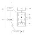
도 6은 본 발명의 일실시예에 따른 전자펜의 블록도이다.
도 7a 및 도 7b는 본 발명의 일실시예에 따른 전자펜의 사용 상태도이다.1A is an exploded perspective view of the pattern film, and FIG. 1B is a cross-sectional view of the pattern film, and FIGS. 1C and 1D are enlarged views of imaginary grid lines, intersection points, and dots of the pattern layer of the pattern film.
2A and 2B are perspective views illustrating a conventional electronic pen.
3 is an exploded perspective view illustrating an electronic pen to which a pen tip is fastened according to an embodiment of the present invention.
4A and 4B are partial cross-sectional views illustrating a state in which a pen tip is fastened according to an embodiment of the present invention.
5 is a schematic diagram showing a contact action according to an embodiment of the present invention.
6 is a block diagram of an electronic pen according to an embodiment of the present invention.
7A and 7B are diagrams illustrating a use state of an electronic pen according to an embodiment of the present invention.
이하에서, 도면을 참조하여 본 발명에 따른 패턴필름 필기용 전자펜에 체결되는 다방향 인식이 가능하도록 하는 펜팁과, 다방향 인식이 가능한 패턴필름 필기용 전자펜을 실시하기 위한 구체적인 내용에 대하여 실시예를 중심으로 상세하게 설명한다.Hereinafter, with reference to the drawings carried out with respect to the pen tip to enable the multi-directional recognition fastened to the pattern film writing electronic pen according to the present invention, and the specific details for implementing the pattern film writing electronic pen capable of multi-directional recognition It demonstrates in detail centering on an example.
먼저 패턴필름(10)에 대해 설명하면, 도트패턴이 형성된 패턴필름(10)은 다층으로 구성되고, 모니터, 노트북, 액정TV 등의 영상기기나 칠판의 전면에 부착되며, 위치정보를 갖는 도트패턴이 형성되어 그 표면 위에 필기되는 전자펜의 필기 궤적의 추적이 가능한 것이고, 이러한 전자펜의 필기가 인식되면서 영상기기나 칠판의 디스플레이 화면에 필기 내용이 표시되는 것이다.First, the
일례로, 도 1a 및 도 1b에 도시된 바와 같이, 패턴필름(10)은 패턴층(20), 확산층(30), 보호층(40), 차단층(50), 점착층(60), 투광층(70)을 포함하여 이루어질 수 있다.For example, as illustrated in FIGS. 1A and 1B, the
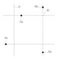
도 1c를 참고하면, 패턴층(20)은 도트(23)들이 가상의 격자선(21)이 교차하는 교차점(22)으로부터 간격을 둔 채 격자선 상에 형성되어 각각의 도트값을 가지며, 이러한 도트값은 적어도 두 개 이상의 상이한 수의 조합으로 구성될 수 있고, 전자펜에 의한 필기시 전자펜(1)의 위치정보를 판단할 수 있도록 위치 정보가 암호화된 미세 패턴에 관한 정보를 갖는다.Referring to FIG. 1C, the
이러한 도트(23)는 프탈로시아닌계 화합물, 나프탈로시아닌계 화합물, 아미늄계 화합물 등을 재료로 하는 적외선 흡수 잉크로 이루어질 수 있고, 각각의 도트는 가상의 격자선(21)의 교차점(22)을 중심으로 형성되는 위치에 따라 결정되는 패턴의 좌표값에 의하여 위치 정보를 제공할 수 있다.The
예컨대, 도 1d를 참고하면 도트는 가상의 격자선(21)의 교차점(22)과의 관계에 따라 4가지 위치에 존재할 수 있는 바, 도트(23a)가 교차점(22) 우측 위치에 존재하는 경우, 도트값을 "1"로, 도트(23b)가 교차점(22)의 상측에 위치하는 경우, 도트값을 "2"로, 도트(23c)가 교차점(22)의 좌측에 위치하는 경우 도트값을 "3"으로, 도트(23d)가 교차점(22)의 하측에 위치하는 경우 도트값을 "4"로 나타냄으로써, 가상의 격자선(21)의 교차점(22)을 중심으로 한 도트의 위치에 따른 위치정보를 제공할 수 있다.For example, referring to FIG. 1D, the dot may exist at four positions according to the relationship with the
또한, 도트는 가상의 격자선(21) 상이 아닌 대각선 방향으로 형성될 수 있고, 하나의 가상의 격자선(21)의 교차점(22)에 다수의 도트들이 형성되어 위치정보를 제공할 수 있으며, 이러한 경우 각각의 도트값은 x좌표와 y좌표로 분리되는 방식으로 임의의 좌표로 표현될 수 있고, 이러한 좌표값으로부터 위치정보가 제공될 수 있다.In addition, the dots may be formed in a diagonal direction instead of on the
이때, 가상의 격자선(21)은 일정한 간격을 따라 가로 및 세로로 형성될 수 있고, 격자선(21) 사이의 거리는 250 내지 300㎛로 형성될 수 있으며, 도트는 가상의 격자선(21)의 교차점(22)을 중심으로 1/8 내지 1/4의 거리를 둔 지점에 형성될 수 있고, 도트는 가상의 격자선(21)의 교차점(22)을 중심으로 두 개 이상의 도트들이 연관되어 형성될 수 있으며, 그 직경은 50 내지 100㎛의 범위이다.At this time, the
확산층(30)은 투명한 재질로 이루어져 패턴층(10)의 전방에 적층 형성되고, 영상기기로부터 발산되는 빛의 일부는 흡수하여 차단함으로써 광포화를 방지하여 전자펜의 센서 인식률이 증가하고 도트패턴의 정확한 위치정보 판단 및 위치결정이 가능하게 되며, 빛의 나머지 일부는 전방측으로 확산시켜 디스플레이 화면에 대한 화상을 흐리게 하거나 콘트라스트를 크게 떨어뜨리지 않고 시인성과 선명도를 증가시킨다. 이를 위하여 확산층(30)은 안티글레어 코팅 처리된 PET가 구비되어 빛이 난반사되지 않고 투과되어 영상기기의 화면이 더욱 선명하게 보일 수 있고, 후방에 접착층이 형성되어 패턴층(20)에 접착이 이루어진다.The
보호층(40)은 확산층(30)의 전방에 형성되고, PET 또는 폴리카보네이트로 이루어져 패턴필름(10)을 보호하고, PET로 이루어진 경우 시트 타입으로써 두루마리가 가능하여 보관 및 이동이 간편하며, 폴리카보네이트의 박판으로 이루어진 경우 두루마리가 가능하지 않지만 플렉서블하게 구부러질 수 있고, 강도와 경도가 증가하여 판서에 의한 보호필름의 손상에 따른 잦은 교체가 필요없고 후술할 투광층(70)이 불필요하게 된다. 보호층(40)은 외표면에 안티글레어 코팅액이 0.1 내지 0.5mm의 두께로 도포 형성되어 빛이 난반사되지 않고 잘 투과되어 영상기기의 화면이 더욱 선명하게 보이고, 필기시 전자펜이 잘 미끄러지지 않고 정확한 판서가 가능해 진다. 더불어, 보호층(40)은 확산층(30) 상에 탈착 가능하게 부착되어 교체 가능하게 구비될 수 있다.The
차단층(50)은 패턴층(20)의 후방에 형성되는 일종의 반사필름으로 사생활을 보호하는 필름과 유사한 것인데, 영상기기로부터 발산되는 빛의 일부를 반사시켜 전방으로 투과되는 것을 차단하는 것이다. 차단층(50)의 광투과율은 65 내지 90%인 것이 바람직하고, 광투과율이 65% 미만이면 디스플레이 화면의 시인도와 밝기가 감소하여 필기가 잘 보이지 않게 되며, 광투과율이 90%를 초과하면 광포화로 인하여 센서의 인식률이 떨어지고 도트 패턴의 이미지가 왜곡되어 위치 정보에 대한 정확한 판독이 곤란하게 된다. 이와 같이 영상기기의 바로 앞에 차단층(50)이 구비되어 영상기기로부터 입사되는 빛의 반사율이 증가하여 영상기기로부터 발산된 빛의 65 내지 90% 정도가 전방으로 투과되므로 전방에서 디스플레이 화면을 충분히 볼 수 있고, 광포화가 방지되어 전자펜의 인식률도 증가하여 전자펜에 의한 도트패턴의 정확한 위치정보 판단 및 위치결정이 가능하게 된다.The blocking
점착층(60)은 차단층(20)의 후방에 형성되어 영상기기나 칠판의 전면에 부착되도록 한다. 또한, 패턴층(20)과 차단층(50) 사이에 투명한 투광층(70)이 형성되어 판넬 타입의 패턴필름(10)으로 제조될 수 있고, 이를 통해 필기시 영상기기의 화면을 보호하고, 강도를 강화시켜 전자펜(1)에 의한 안정적인 판서가 가능해진다. 이때, 투광층(70)은 아크릴판, 폴리카보네이트판 및 유리판에서 선택된 어느 하나로 이루어질 수 있다. 이와 같이, 패턴층(20)의 전후면에 각각 확산층(30) 및 차단층(50)을 이중으로 부착하여 영상기기로부터 발산되는 빛의 일부를 흡수 또는 반사시켜 전자펜의 인식률을 증가시킴과 동시에 빛의 일부는 투과 및 확산시켜 디스플레이 화면의 화상을 흐리게 하거나 콘트라스트를 크게 떨어뜨리지 않고 시인성과 선명도가 증가되는 것이다.The
도 2a 및 도 2b를 참고하면, 종래의 도트패턴이 형성된 패턴필름 필기용 전자펜(1)은 도트패턴이 형성된 패턴필름(10) 위에 필기되어 필기 궤적이 추적되고, 필기 내용이 인식되면서 외부 디바이스(D)의 디스플레이 화면에 표시되는데 사용하는 전자펜으로, 본체부(200)는 합성수지 재질이고, 대략 외주면이 라운드진 원통형으로 이루어지며, 중간에 다소 돌출되어 다른 부분보다 직경이 증가하도록 볼록부(201)가 형성되고, 볼록부(201)의 상·하측에 각각 상부 경사면(202)과 하부 경사면(203)이 평평하게 형성되며, 상부 경사면(202)과 하부 경사면(203)은 사용자가 전자펜(1)을 파지하여 필기시 손의 중지면 말단과 검지면에 각각 지지되어 힘을 가할 수 있고, 정확한 필기가 가능하도록 한다. 본체부(200)는 상부에 전원홈(204)이 형성되고, 전원홈(204)의 내측에 버튼식 전원스위치(205)가 형성되어 전원스위치(205)의 임의 조작이 방지될 수 있다. 종래의 전자펜(1)의 단부에는 펜팁(1a)이 형성되고, 펜팁(1a)에는 길이 방향으로 길게 형성된 펜촉(1b)이 장착되어 본체부(200)까지 연장 형성되며, 펜촉(1b)에 의해 필기가 이루어진다.Referring to FIGS. 2A and 2B, the
또한, 도 6을 참고하면 본체부(200)는 내부에 광원(220)과 센서(230), 통신모듈(240) 및 제어모듈(250)이 형성된다. 광원(220)은 외부로 적외선을 투광시켜 방출하고, 센서(230)는 적외선 센서로서 패턴층(20)의 도트가 형성되지 않은 부분에서 산란되는 적외선을 감지하여 패턴층(20)에 형성된 도트들의 패턴정보를 연속적으로 센싱한 후 제어모듈(250)이 절대 좌표값을 계산하여 위치정보를 산출할 수 있다. 예컨대, 6x6 크기의 가상의 격자선(21) 상에서 가로와 세로 6개씩 36개의 도트들을 인식한 경우, 센서(230)가 적외선을 감지하여 패턴층(20)에 형성된 도트들의 패턴정보를 연속적으로 센싱한 후 제어모듈(250)이 각각의 도트값에 따른 위치 정보를 산출하고 이를 이용하여 패턴필름(10) 상의 절대 좌표값을 파악할 수 있는 것이다.In addition, referring to FIG. 6, the
상기 통신모듈(240)은 본체부(200)에 내장되고, wifi, 블루투스 등의 단거리 무선 통신이 가능하며, 이로써 센서(230)에 의해 센싱된 좌표값은, 제어모듈(250)에 의해 분석된 후 통신모듈(240)를 통해 컴퓨터, 노트북, 액정TV, 스마트폰 등의 외부 디바이스(D)로 전송되어 디스플레이 화면에 표시되거나, 통신모듈(240)에 의하여 컴퓨터, 노트북, 액정TV, 스마트폰 등의 외부 디바이스(D)로 전송되어 외부 디바이스의 프로세서에 의해 좌표값이 분석된 후 전자펜(1)이 위치한 실제 좌표값이 계산되어 디스플레이 화면에 표시될 수 있다.The
또한, 본체부(200)는, 내부에 충전 가능한 배터리(260)가 내장될 수 있고, 상단부에 충전단자(206)가 형성되어 배터리(260)에 대한 충전이 가능하다. 또한, 본체부(200)는, 상부에 충전표시등(207)이 형성되어 충전중일때 표시가 되고, 중간부에 상태표시등(208)이 형성되어 작동중, 배터리부족 등에 관한 여러 가지 상태를 표시하며, 상부에 블루투스 표시등(209)이 형성되어 블루투스 연결 상태를 표시한다.In addition, the
그런데, 이러한 전자펜(1)은 펜촉(1b)이 한 방향으로 치우쳐 형성되도록 펜팁(1a)의 구조를 갖고 있어 특정한 방향으로 기울여 사용해야만 센서(230)의 필기 인식이 가능하게 되고, 전자펜(1)을 회전하여 다른 방향으로 기울여 사용할 경우 펜팁(1a) 근처에 음영 면적이 증가하고, 센서를 비추는 외부 빛의 밝기가 약해져서 센서의 인식률이 떨어지며, 이에 따라 패턴 이미지에 대한 정확한 식별이 곤란해 지고, 사용이 매우 불편하며, 광원에서 발산된 빛이 대부분 외부로 반사되거나 펜팁(1a)에 흡수되어 광학 센서로 되돌아오는 양이 적기 때문에 위치 결정 및 해독에 문제가 많이 발생하였다.However, the
이에, 본 발명자는 도 2a 및 도 2b와 같이 종래의 전자펜(1)의 본체부(200) 선단에 연결된 펜팁(1a)의 일부를 절개선(S)을 따라 절개하여 절개부(300)를 형성하고, 상기 절개부(300)에 새로운 구조를 갖는 본 발명의 펜팁(100)을 체결하여 전자펜의 360도 회전이 자유롭고 다방향 인식이 가능하여 어떤 방향으로도 기울여 사용할 수 있도록 하였다.Thus, the present inventors cut a portion of the
이를 위하여, 도 3을 참고하면 상기 펜팁(100)은 패턴필름(10) 상에 접촉하여 필기하는 펜팁부(110)와, 상기 펜팁부(110)에 연결 형성되고 전자펜(1)의 절개부(300)의 외주면을 감싸 체결하는 커버부(120)를 포함하여 이루어진다.To this end, referring to FIG. 3, the
상기 펜팁부(110)는 천연고무나 합성고무와 같은 연질의 탄성 재질로 이루어지고, 대략 꼭지부가 잘린 역원추형으로 이루어져 내부가 중공 형성되며, 펜팁이 전자펜에 체결된 상태를 기준으로 끝단(하단) 중앙에 원형의 펜홀(111)이 관통 형성되고, 펜홀(111)의 테두리(111a)가 패턴필름(10) 상에 직접 접촉되어 필기가 이루어진다. 이때 펜홀(111)의 크기는 반경이 1.5 내지 6mm의 크기로 형성될 수 있으며, 반경이 1.5mm 미만이면 광원이 충분히 비추지 못하여 패턴 이미지에 대한 정확한 식별이 곤란할 수 있고, 반경이 6mm를 초과하면 펜끝이 너무 확장되어 필기가 불편할 수 있다.The
또한, 도 5를 참고하면 상기 펜팁부(110)는 전자펜(1)의 내측에 삽입되는 접점핀(210)의 일단부(하단부)가 연결되고, 접점핀(210)의 타단부(상단부)는 제어모듈(250)의 회로와 연결된 접점단자(270)와 약간의 간격을 유지하도록 배치된다. 이때, 상기 접점핀(210)의 타단부에는 카본블랙 성분을 포함한 도전성 고무(211)가 형성될 수 있다. 이러한 전자펜의 접점에 의해 감지는 대한민국 등록특허공보 제10-0904170호를 비롯한 선행문헌에 이미 공지된 기술이므로 여기서 자세한 설명은 생략한다.In addition, referring to FIG. 5, the
더불어, 종래의 전자펜(1)의 펜촉(1b)을 접점핀(210)으로 이용하여 펜팁(100)을 접점핀(210)에 연결하거나, 접점핀(210)이 미리 구비된 펜팁(100)을 전자펜(1)의 절개부(300)에 체결하여 접점핀(210)이 전자펜(1)의 본체부(200)에 장착되도록 할 수도 있다.In addition, the
펜팁부(110)의 끝단에 가해지는 필압에 따라 접점핀(210)이 승강 이동하게 되는 바, 사용자가 전자펜(1)으로 패턴필름(10) 상에 필기하여 글씨 또는 그림 등을 작성할 때에 펜팁부(110)의 끝단에 가해지는 압력으로 인하여 연질의 탄성 재질로 이루어진 펜팁부(110)가 약간 압축되고, 압축된 펜팁부(110)의 필압이 펜팁부(110)와 일단부가 연결된 접점핀(210)에 전달된 후, 접점핀(210) 타단부의 도전성 고무(211)가 전자펜(1)의 접점단자(270)와 접촉되어 통전되면 제어모듈(250)이 이를 감지하여 광원(220)에서 적외선을 발진시키고 센서(230)로부터 패턴필름(10)에서 산란되는 적외선을 감지하여 도트들의 패턴정보를 센싱하여 패턴정보를 분석하여 위치정보를 산출하게 되는 것이다.The
반면에, 필기 도중 또는 필기가 끝나서 전자펜(1)의 펜팁부(1110)가 패턴필름(10)에서 분리되는 경우(필기가 중단되는 경우), 연질의 탄성 재질로 이루어진 펜팁부(110)가 다시 원래되로 신장 복원되면서 펜팁부(110)에 일단부가 연결된 접점핀(210) 타단부의 도전성 고무(211)가 접점단자(270)로부터 비접촉되어 멀어지게 되어 비통전 상태가 되면 제어모듈(250)이 광원(220)에서 적외선 발진을 단락시켜 필기를 해도 필기가 감지되지 않게 되는 것이다.On the other hand, when the pen tip 1110 of the
따라서, 패턴필름(10) 상에 펜팁부(110)가 접촉되어 필기하는 경우에만 필기가 감지되고, 패턴필름(10)에서 펜팁부(110)를 분리하면 적외선이 발진이 단락되므로 정확하게 글씨나 그림을 작성할 수 있고, 자유로운 전자 판서가 가능하게 된다.Therefore, writing is sensed only when the
또한, 도 4a 및 도 4b를 참고하면 상기 펜팁부(110)는 내주면에 합성수지와 같은 경질로 이루어진 내주링(130)이 형성될 수 있다. 펜팁부(110)가 연질로 이루어져 있기 때문에 접점핀(210)의 반대쪽 테두리(111a)로 패턴필름(10) 상에 필기하는 경우 필압이 접점핀(210)에 잘 전달되지 않을 수 있으므로 경질의 내주링(130)을 형성하여 테두리(111a)의 어느 방향으로 필기하더라도 필압이 접점핀(210)에 잘 전달되어 필기 인식률을 크게 증가시킬 수 있다. 이때, 상기 내주링(130)은 소정의 각도로 기울어져 형성되되, 접점핀(210)의 일단부에서 하측을 향해 소정의 각도로 기울어져 형성됨으로써, 접점핀(210)의 반대쪽 테두리(111a)로 필기하더라도 필압이 접점핀(210)에 더욱 잘 전달될 수 있도록 하는 것이 바람직하다.4A and 4B, the
또한, 전자펜(1)의 절개부(300)는 내측으로 돌출된 돌출턱(310)이 링 형상으로 형성되고, 접점핀(210)이 상기 돌출턱(310)을 관통하여 지지되며, 상기 펜팁부(110)는 외측의 외측부(112)와 내측의 내측부(113)로 이루어질 수 있다.In addition, the
상기 외측부(112)는 상단부가 상기 돌출턱(310)에 접촉 지지되어 필기시 필압에 의해 펜팁(100)이 임의로 움직이거나 본체부(200)로 삽입되지 않도록 하고, 하단부의 테두리(111a)는 패턴필름(10)과 접촉되어 필기가 이루어진다. The
상기 내측부(113)는 상기 외측부(112)의 내측에 형성되고, 상기 내측부(113)의 상단부가 돌출턱(310)과 소정의 유격(114)을 갖고 이격되도록 외측부(112)의 상단부에 대해 단차(115)가 형성되며, 상기 유격(114)은 0.1 내지 1mm의 미세한 틈새로 형성된다. 이로써, 유격(114)으로 인해 필기시 필압에 의해 펜팁부(110)의 압축이 용이하게 이루어질 수 있고, 압축시 내측부(113)의 상단부가 돌출턱(310)에 의해 스토핑되어 과도한 압축을 방지하고 완충 작용을 한다.The
상기 내측부(113)는 내측면에 빛과 적외선을 반사시키는 반사물질이 도포된 도포층(113a)이 형성될 수 있다. 이때, 상기 반사물질은 세라믹, 알루미늄, 구리, 주석, 은, 금, 백금 등의 금속이거나, 백색의 플라스틱, 백색의 종이, 백색의 고무 등으로 이루어져 빛이 흡수되지 않고 반사가 잘 이루어지며, 도포층(113a)은 빛과 적외선이 센서(230)를 향하도록 모아주어 센서(230)의 인식률이 증가함으로써 도트패턴에 대한 정확한 위치 결정 및 해독이 가능하게 되고, 주변의 빛과 외부 디바이스(D)로부터 발산된 빛을 모아서 센서를 밝게 해 주므로 전자펜(1)을 소정의 각도로 기울여 펜팁부(110) 주변이 다소 어두워지더라도 센서(230)의 인식률이 저하되지 않고 패턴 이미지의 식별이 가능하게 된다.The
또한, 상기 펜팁부(110)의 일부가 사용에 의해 마모된 경우 제2펜팁부(미도시)를 상기 펜팁부(110)의 외주면에 감싸 체결하여 내구성을 증가시킬 수 있다. 상기 제2펜팁부도 상기 펜팁부(110)처럼 연질의 탄성 재질로 이루어지고, 내부가 중공 형성되며, 끝단 중앙에 펜홀이 관통 형성되고, 펜홀의 테두리가 패턴필름과 직접 접촉되어 필기가 이루어진다. 이때, 상기 제2펜팁부는 커버부(120)로 감싸여 지지 않은 펜팁부(110)의 노출된 나머지 부분을 감쌀 수 있는 크기와 직경으로 이루어지는 것이 바람직하며, 펜팁부(110)에 끼워져 체결될 수 있다.In addition, when a part of the
상기 커버부(120)는 일부는 펜팁부(110)의 외주면 일부분을 감싸도록 펜팁부(110)에 연결되고, 나머지는 본체부(200)의 외주면 일부와 절개부(300)의 외주면을 감싸도록 체결된다.The
아울러, 상기 덮개부(400)는 전자펜(1)의 미사용시 펜팁(100)를 덮어 보호할 수 있다.In addition, the
도 7a에 도시된 바와 같이, 태블릿PC의 외부 디바이스(D)에 패턴필름(10)을 부착하여 전자펜(1)으로 필기할 때, 도 7b에 도시된 바와 같이 전자펜(1)을 여러 방향과 각도로 기울여 필기하더라도 광원(220)에서 패턴필름(10)을 향해 투광되어 방출된 적외선이 패턴필름(10)의 도트가 형성되지 않은 부분에서 산란된 후 다시 상측으로 반사되어 센서(230)로 되돌아가 센싱될 수 있으므로 도트패턴에 대한 이미지가 식별되어 정확한 위치 결정 및 해독을 통해 외부 디바이스(D)의 디스플레이 화면에 필기 내용이 정확히 표시되고, 사용 범위가 크게 증가하며, 360도로 자유롭게 회전이 가능하여 필기가 용이하고 사용 편의성이 증가하게 된다.As shown in FIG. 7A, when the
결국, 본 발명에 따른 패턴필름 필기용 전자펜에 체결되는 다방향 인식이 가능하도록 하는 펜팁(100)과, 다방향 인식이 가능한 패턴필름 필기용 전자펜(1)은 기존 전자펜의 구조를 개선하여 전자펜의 360도 회전이 자유롭고 다방향 인식을 가능케 함으로써, 전자펜을 다양한 방향과 각도로 기울여 사용하더라도 도트패턴에 대한 이미지가 식별되어 정확한 위치 결정및 해독이 가능하고, 사용 범위가 크게 증가하며, 필기가 용이하여 사용 편의성이 증가하고, 필기 중단시 적외선이 단락되어 정확하게 필기할 수 있고 자유롭게 판서할 수 있는 것이다.As a result, the
본 발명에서 상기 실시 형태는 하나의 예시로서 본 발명이 여기에 한정되는 것은 아니다. 본 발명의 청구범위에 기재된 기술적 사상과 실질적으로 동일한 구성을 갖고 동일한 작용효과를 이루는 것은 어떠한 것이라도 본 발명의 기술적 범위에 포함된다.In the present invention, the above embodiment is an example, and the present invention is not limited thereto. Anything that has substantially the same configuration and achieves the same effect as the technical idea described in the claims of the present invention is included in the technical scope of the present invention.
1. 전자펜 1a. 종래의 펜팁
1b. 펜촉 10. 패턴필름
20. 패턴층 21. 격자선
22. 교차 점 23.23a,23b,23c,23d. 도트
30. 확산층 40. 보호층
50. 차단층 60. 점착층
70. 투광층 100. 펜팁
110. 펜팁부 111. 펜홀
111a. 테두리 112. 외측부
113. 내측부 113a. 도포층
114. 유격 115. 단차
120. 커버부 130. 내주링
200. 본체부 201. 볼록부
202. 상부 경사면 203. 하부 경사면
204. 전원홈 205. 전원스위치
206. 충전단자 207. 충전표시등
208. 상태표시등 209. 블루투스 표시등
210. 접점핀 211. 도전성고무
220. 광원 230. 센서
240. 통신모듈 250. 제어모듈
260. 배터리 270. 접점단자
300. 절개부 310. 돌출턱
400. 덮개부 D. 외부 디바이스
S. 절개선1.
1b.
20.
22. Intersection 23.23a, 23b, 23c, 23d. dot
30.
50.
70.
110.
111a.
113.
114.Gap 115.Gap
120. Cover
200.
202.
204.
206. Charging
208.
210.
220.
240.
260.
300.
400. Cover part D. External device
S. Incision
Claims (9)
Translated fromKorean연질의 탄성 재질로 이루어지고, 내부가 중공 형성되며, 끝단 중앙에 펜홀이 관통 형성되고, 전자펜의 내측에 삽입되는 접점핀의 일단부가 연결되며, 내주면에 경질의 내주링이 형성되고, 펜홀의 테두리가 상기 패턴필름과 직접 접촉되어 필기가 이루어지는 펜팁부; 및
상기 펜팁부에 연결 형성되고 전자펜의 절개부의 외주면을 감싸 체결하는 커버부를 포함하되,
패턴필름 상에 필기시 압축된 펜팁부의 필압이 접점핀에 전달된 후 접점핀이 전자펜의 접점단자와 접촉되어 필기가 감지되고, 펜팁부를 패턴필름에서 분리시 펜팁부가 복원되어 접점핀이 접점단자와 비접촉되어 필기가 감지되지 않는 것을 특징으로 하는, 패턴필름 필기용 전자펜에 체결되는 다방향 인식이 가능하도록 하는 펜팁.
By writing on a pattern film with a dot pattern, the trace is traced and the incision is made by cutting the end of the electronic pen to be displayed on the screen of the external device as the writing is recognized, and is fastened to the cutout.
Made of soft elastic material, the inside is hollow, pen hole is formed through the center of the end, one end of the contact pin inserted into the inside of the electronic pen is connected, a hard inner circumference ring is formed on the inner peripheral surface, A pen tip portion in which an edge is directly contacted with the pattern film to write; And
Is formed connected to the pen tip portion and includes a cover to wrap and fasten the outer peripheral surface of the incision of the electronic pen,
When writing on the pattern film, the pen pressure of the compressed pen tip is transferred to the contact pin, and then the contact pin is contacted with the contact terminal of the electronic pen and writing is detected.When the pen tip is separated from the pattern film, the pen tip is restored and the contact pin is the contact terminal. The pen tip to enable a multi-directional recognition that is fastened to the electronic pen for pattern film writing, characterized in that the writing is not detected in contact with.
연질의 탄성 재질로 이루어지고, 내부가 중공 형성되며, 끝단 중앙에 펜홀이 관통 형성되고, 전자펜의 내측에 삽입되는 접점핀의 일단부가 연결되며, 펜홀의 테두리가 상기 패턴필름과 직접 접촉되어 필기가 이루어지는 펜팁부;
상기 펜팁부의 일부가 마모된 경우 상기 펜팁부의 외주면에 체결되는 제2펜팁부; 및
상기 펜팁부에 연결 형성되고 전자펜의 절개부의 외주면을 감싸 체결하는 커버부를 포함하되,
패턴필름 상에 필기시 압축된 펜팁부의 필압이 접점핀에 전달된 후 접점핀이 전자펜의 접점단자와 접촉되어 필기가 감지되고, 펜팁부를 패턴필름에서 분리시 펜팁부가 복원되어 접점핀이 접점단자와 비접촉되어 필기가 감지되지 않는 것을 특징으로 하는, 패턴필름 필기용 전자펜에 체결되는 다방향 인식이 가능하도록 하는 펜팁.
By writing on a pattern film with a dot pattern, the trace is traced and the incision is made by cutting the end of the electronic pen to be displayed on the screen of the external device as the writing is recognized, and is fastened to the cutout.
It is made of a soft elastic material, the inside is hollow, the pen hole is formed through the center of the tip, one end of the contact pin inserted into the inside of the electronic pen is connected, the edge of the pen hole is in direct contact with the pattern film to write Pen tip portion is made;
A second pen tip part fastened to an outer circumferential surface of the pen tip part when a part of the pen tip part is worn; And
Is formed connected to the pen tip portion and includes a cover to wrap and fasten the outer peripheral surface of the incision of the electronic pen,
When writing on the pattern film, the pen pressure of the compressed pen tip is transferred to the contact pin, and then the contact pin is contacted with the contact terminal of the electronic pen and writing is detected.When the pen tip is separated from the pattern film, the pen tip is restored and the contact pin is the contact terminal. The pen tip to enable a multi-directional recognition that is fastened to the electronic pen for pattern film writing, characterized in that the writing is not detected in contact with.
상기 내주링은 접점핀의 일단부에서 하측으로 소정의 각도로 기울어져 형성된 것을 특징으로 하는 패턴필름 필기용 전자펜에 체결되는 다방향 인식이 가능하도록 하는 펜팁.
The method of claim 1,
The inner circumferential ring is a pen tip to enable a multi-directional recognition that is fastened to the pattern film writing electronic pen, characterized in that formed inclined at a predetermined angle downward from one end of the contact pin.
상기 펜팁부는 전자펜의 절개부에 접촉 지지되는 외측부와, 상기 외측부의 내측에 형성되어 절개부와 소정의 유격을 갖고 이격되도록 외측부에 대해 단차가 형성된 내측부를 포함하는 다방향 인식이 가능하도록 하는 펜팁.
The method according to claim 1 or 2,
The pen tip part may include a pen tip which includes an outer part contacted and supported by an incision of the electronic pen, and an inner part formed on an inner side of the outer part and having a step with respect to the outer part so as to be spaced apart from the incision with a predetermined clearance. .
전자펜의 펜촉을 접점핀으로 이용하거나, 접점핀이 구비된 펜팁을 전자펜의 절개부에 체결하는 것을 특징으로 하는 다방향 인식이 가능하도록 하는 펜팁.
The method according to claim 1 or 2,
Using a pen tip of the electronic pen as a contact pin, or pen tip to enable a multi-directional recognition, characterized in that to fasten the pen tip provided with the contact pin to the incision of the electronic pen.
상기 펜팁부는 내주면에 빛과 적외선을 반사시키는 반사물질이 도포된 도포층이 형성되며,
상기 반사물질은 세라믹, 알루미늄, 구리, 주석, 은, 금, 백금, 백색의 플라스틱, 백색의 종이, 백색의 고무에서 선택된 어느 하나로 이루어진 것을 특징으로 하는 패턴필름 필기용 전자펜에 체결되는 다방향 인식이 가능하도록 하는 펜팁.
The method according to claim 1 or 2,
The pen tip portion is formed with a coating layer coated with a reflective material reflecting light and infrared rays on the inner peripheral surface,
The reflective material is a multi-directional recognition fastened to the pattern film writing electronic pen, characterized in that any one selected from ceramic, aluminum, copper, tin, silver, gold, platinum, white plastic, white paper, white rubber. Pen tip to make this possible.
전원스위치, 외부 디바이스와 무선 통신하는 통신모듈, 외부로 적외선을 투광시켜 방출하는 광원, 패턴필름에서 산란되는 적외선을 감지하여 도트들의 패턴정보를 센싱하는 센서, 및 센싱된 패턴정보를 분석하여 위치정보를 산출하는 제어모듈이 설치된 본체부;
전자펜의 본체부 선단에 연결된 펜팁의 일부를 절개하여 형성된 절개부; 및
상기 절개부에 체결되는 제 1항 내지 제 3항에서 선택된 어느 한 항의 펜팁을 포함하는, 다방향 인식이 가능한 패턴필름 필기용 전자펜.
An electronic pen that writes on a pattern film on which a dot pattern is formed so that a trace is traced and the writing is recognized and displayed on a screen of an external device.
A power switch, a communication module for wireless communication with an external device, a light source that emits infrared light to the outside, a sensor for sensing pattern information of dots by detecting infrared light scattered from the pattern film, and location information by analyzing the sensed pattern information Body unit is installed to calculate the control module;
An incision formed by cutting a portion of the pen tip connected to the distal end of the electronic pen; And
An electronic pen for pattern film writing capable of multi-directional recognition, comprising a pen tip of any one of claims 1 to 3 fastened to the incision.
전자펜의 절개부는 내측으로 돌출된 돌출턱이 형성되고, 상기 돌출턱은 접점핀이 관통되며,
상기 펜팁부는, 외측부가 돌출턱에 접촉 지지되며, 내측부는 돌출턱과 소정의 유격을 갖고 이격되도록 형성된 것을 특징으로 하는 다방향 인식이 가능한 패턴필름 필기용 전자펜.
The method of claim 8,
An incision portion of the electronic pen is formed with a protruding jaw protruding inward, and the protruding jaw is penetrated by a contact pin.
The pen tip portion, the outer side is supported in contact with the protruding jaw, the inner portion of the pattern film writing electronic pen capable of recognizing multi-directional recognition, characterized in that formed so as to be spaced apart from the protruding jaw.
Priority Applications (1)
| Application Number | Priority Date | Filing Date | Title |
|---|---|---|---|
| KR1020190056265AKR102069745B1 (en) | 2019-05-14 | 2019-05-14 | Pentip for multi-direction recognition combinating on electronic pen for writing on pettern film and electronic pen having multi-direction recognition for writing on pattern film |
Applications Claiming Priority (1)
| Application Number | Priority Date | Filing Date | Title |
|---|---|---|---|
| KR1020190056265AKR102069745B1 (en) | 2019-05-14 | 2019-05-14 | Pentip for multi-direction recognition combinating on electronic pen for writing on pettern film and electronic pen having multi-direction recognition for writing on pattern film |
Publications (1)
| Publication Number | Publication Date |
|---|---|
| KR102069745B1true KR102069745B1 (en) | 2020-01-23 |
Family
ID=69368876
Family Applications (1)
| Application Number | Title | Priority Date | Filing Date |
|---|---|---|---|
| KR1020190056265AActiveKR102069745B1 (en) | 2019-05-14 | 2019-05-14 | Pentip for multi-direction recognition combinating on electronic pen for writing on pettern film and electronic pen having multi-direction recognition for writing on pattern film |
Country Status (1)
| Country | Link |
|---|---|
| KR (1) | KR102069745B1 (en) |
Cited By (2)
| Publication number | Priority date | Publication date | Assignee | Title |
|---|---|---|---|---|
| KR200495951Y1 (en)* | 2022-06-10 | 2022-09-29 | 주식회사 보나 | Pen tip module device for optical electronic pen |
| KR102872863B1 (en) | 2020-09-07 | 2025-10-17 | (주)네오랩컨버전스 | A method of printing code pattern on repositionalbe sheet |
Citations (7)
| Publication number | Priority date | Publication date | Assignee | Title |
|---|---|---|---|---|
| WO2001026032A1 (en) | 1999-10-01 | 2001-04-12 | Anoto Ab | Encoded paper for optical reading |
| KR20010067896A (en)* | 2000-12-15 | 2001-07-13 | 양홍영 | A pen type light mouse device |
| KR20070040408A (en)* | 2004-08-03 | 2007-04-16 | 실버브룩 리서치 피티와이 리미티드 | Electronic stylus |
| JP4008952B2 (en)* | 2004-05-24 | 2007-11-14 | 健治 吉田 | Dot pattern reading unit and mouse equipped with the same |
| KR20140029643A (en)* | 2012-08-29 | 2014-03-11 | 주식회사 네오랩컨버전스 | Electronic chalk |
| KR20150042901A (en)* | 2013-10-13 | 2015-04-22 | 김병창 | Ear pick emitted sequentially disposable swab |
| US20150286293A1 (en)* | 2014-04-03 | 2015-10-08 | Qualcomm Incorporated | Optical stylus with deformable tip |
- 2019
- 2019-05-14KRKR1020190056265Apatent/KR102069745B1/enactiveActive
Patent Citations (7)
| Publication number | Priority date | Publication date | Assignee | Title |
|---|---|---|---|---|
| WO2001026032A1 (en) | 1999-10-01 | 2001-04-12 | Anoto Ab | Encoded paper for optical reading |
| KR20010067896A (en)* | 2000-12-15 | 2001-07-13 | 양홍영 | A pen type light mouse device |
| JP4008952B2 (en)* | 2004-05-24 | 2007-11-14 | 健治 吉田 | Dot pattern reading unit and mouse equipped with the same |
| KR20070040408A (en)* | 2004-08-03 | 2007-04-16 | 실버브룩 리서치 피티와이 리미티드 | Electronic stylus |
| KR20140029643A (en)* | 2012-08-29 | 2014-03-11 | 주식회사 네오랩컨버전스 | Electronic chalk |
| KR20150042901A (en)* | 2013-10-13 | 2015-04-22 | 김병창 | Ear pick emitted sequentially disposable swab |
| US20150286293A1 (en)* | 2014-04-03 | 2015-10-08 | Qualcomm Incorporated | Optical stylus with deformable tip |
Cited By (2)
| Publication number | Priority date | Publication date | Assignee | Title |
|---|---|---|---|---|
| KR102872863B1 (en) | 2020-09-07 | 2025-10-17 | (주)네오랩컨버전스 | A method of printing code pattern on repositionalbe sheet |
| KR200495951Y1 (en)* | 2022-06-10 | 2022-09-29 | 주식회사 보나 | Pen tip module device for optical electronic pen |
Similar Documents
| Publication | Publication Date | Title |
|---|---|---|
| KR200485305Y1 (en) | Electronic pen for writing on pattern film having dot pattern | |
| KR102073000B1 (en) | Electronic pen for writing on pattern film | |
| KR101686466B1 (en) | Information input system, and information input assistance sheet | |
| EP2479650B1 (en) | Product with coding pattern | |
| KR20100137433A (en) | Digital pens and methods for digitally recording information | |
| KR20130095264A (en) | Display with coding pattern | |
| US8243028B2 (en) | Eraser assemblies and methods of manufacturing same | |
| KR101836075B1 (en) | Information input assistance sheet | |
| US8890842B2 (en) | Eraser for use with optical interactive surface | |
| US20090309854A1 (en) | Input devices with multiple operating modes | |
| US20140362054A1 (en) | Display control system and reading device | |
| TWI657367B (en) | Touch display device and touch position detecting system | |
| US20130321357A1 (en) | Display panel and display device | |
| JP2010026693A (en) | Information input device, image display, and stylus pen | |
| KR102069745B1 (en) | Pentip for multi-direction recognition combinating on electronic pen for writing on pettern film and electronic pen having multi-direction recognition for writing on pattern film | |
| US11625106B2 (en) | Films or surfaces including positional tracking marks | |
| US20080122790A1 (en) | Optical handwriting input device | |
| US9170684B2 (en) | Optical navigation device | |
| US9128538B2 (en) | Optical film, display panel, and display device | |
| KR100489959B1 (en) | Structure of optical pen type pointing device | |
| JPWO2013161245A1 (en) | Display control system, display device, and display panel | |
| JP2007133824A (en) | Handwriting input system, electronic pen device and position coordinate encoding medium applied to the same | |
| JP2016081180A (en) | Electronic pen sheet, electronic pen display device | |
| US20140098070A1 (en) | Stylus body having two or more spheres coaxially affixed thereto | |
| KR20240172307A (en) | Optical pen and display system including optical interface |
Legal Events
| Date | Code | Title | Description |
|---|---|---|---|
| PA0109 | Patent application | Patent event code:PA01091R01D Comment text:Patent Application Patent event date:20190514 | |
| PA0201 | Request for examination | ||
| PA0302 | Request for accelerated examination | Patent event date:20190514 Patent event code:PA03022R01D Comment text:Request for Accelerated Examination | |
| PE0902 | Notice of grounds for rejection | Comment text:Notification of reason for refusal Patent event date:20190925 Patent event code:PE09021S01D | |
| PE0902 | Notice of grounds for rejection | Comment text:Final Notice of Reason for Refusal Patent event date:20191121 Patent event code:PE09021S02D | |
| E701 | Decision to grant or registration of patent right | ||
| PE0701 | Decision of registration | Patent event code:PE07011S01D Comment text:Decision to Grant Registration Patent event date:20200110 | |
| GRNT | Written decision to grant | ||
| PR0701 | Registration of establishment | Comment text:Registration of Establishment Patent event date:20200117 Patent event code:PR07011E01D | |
| PR1002 | Payment of registration fee | Payment date:20200117 End annual number:3 Start annual number:1 | |
| PG1601 | Publication of registration | ||
| G170 | Re-publication after modification of scope of protection [patent] | ||
| PG1701 | Publication of correction | Patent event code:PG17011E01I Patent event date:20200211 Comment text:Request for Publication of Correction Publication date:20200214 | |
| PR1001 | Payment of annual fee | Payment date:20230117 Start annual number:4 End annual number:4 | |
| PR1001 | Payment of annual fee | Payment date:20240117 Start annual number:5 End annual number:5 |