KR102060742B1 - Package structures and methods of forming the same - Google Patents
Package structures and methods of forming the sameDownload PDFInfo
- Publication number
- KR102060742B1 KR102060742B1KR1020170143777AKR20170143777AKR102060742B1KR 102060742 B1KR102060742 B1KR 102060742B1KR 1020170143777 AKR1020170143777 AKR 1020170143777AKR 20170143777 AKR20170143777 AKR 20170143777AKR 102060742 B1KR102060742 B1KR 102060742B1
- Authority
- KR
- South Korea
- Prior art keywords
- die
- component
- substrate
- dummy
- memory
- Prior art date
- Legal status (The legal status is an assumption and is not a legal conclusion. Google has not performed a legal analysis and makes no representation as to the accuracy of the status listed.)
- Active
Links
Images


Classifications
- H—ELECTRICITY
- H01—ELECTRIC ELEMENTS
- H01L—SEMICONDUCTOR DEVICES NOT COVERED BY CLASS H10
- H01L23/00—Details of semiconductor or other solid state devices
- H01L23/28—Encapsulations, e.g. encapsulating layers, coatings, e.g. for protection
- H01L23/31—Encapsulations, e.g. encapsulating layers, coatings, e.g. for protection characterised by the arrangement or shape
- H01L23/3107—Encapsulations, e.g. encapsulating layers, coatings, e.g. for protection characterised by the arrangement or shape the device being completely enclosed
- H01L23/3114—Encapsulations, e.g. encapsulating layers, coatings, e.g. for protection characterised by the arrangement or shape the device being completely enclosed the device being a chip scale package, e.g. CSP
- H—ELECTRICITY
- H01—ELECTRIC ELEMENTS
- H01L—SEMICONDUCTOR DEVICES NOT COVERED BY CLASS H10
- H01L25/00—Assemblies consisting of a plurality of semiconductor or other solid state devices
- H01L25/50—Multistep manufacturing processes of assemblies consisting of devices, the devices being individual devices of subclass H10D or integrated devices of class H10
- H—ELECTRICITY
- H01—ELECTRIC ELEMENTS
- H01L—SEMICONDUCTOR DEVICES NOT COVERED BY CLASS H10
- H01L21/00—Processes or apparatus adapted for the manufacture or treatment of semiconductor or solid state devices or of parts thereof
- H01L21/02—Manufacture or treatment of semiconductor devices or of parts thereof
- H01L21/04—Manufacture or treatment of semiconductor devices or of parts thereof the devices having potential barriers, e.g. a PN junction, depletion layer or carrier concentration layer
- H01L21/48—Manufacture or treatment of parts, e.g. containers, prior to assembly of the devices, using processes not provided for in a single one of the groups H01L21/18 - H01L21/326 or H10D48/04 - H10D48/07
- H01L21/4814—Conductive parts
- H01L21/4846—Leads on or in insulating or insulated substrates, e.g. metallisation
- H01L21/486—Via connections through the substrate with or without pins
- H—ELECTRICITY
- H01—ELECTRIC ELEMENTS
- H01L—SEMICONDUCTOR DEVICES NOT COVERED BY CLASS H10
- H01L21/00—Processes or apparatus adapted for the manufacture or treatment of semiconductor or solid state devices or of parts thereof
- H01L21/02—Manufacture or treatment of semiconductor devices or of parts thereof
- H01L21/04—Manufacture or treatment of semiconductor devices or of parts thereof the devices having potential barriers, e.g. a PN junction, depletion layer or carrier concentration layer
- H01L21/50—Assembly of semiconductor devices using processes or apparatus not provided for in a single one of the groups H01L21/18 - H01L21/326 or H10D48/04 - H10D48/07 e.g. sealing of a cap to a base of a container
- H01L21/56—Encapsulations, e.g. encapsulation layers, coatings
- H01L21/561—Batch processing
- H—ELECTRICITY
- H01—ELECTRIC ELEMENTS
- H01L—SEMICONDUCTOR DEVICES NOT COVERED BY CLASS H10
- H01L21/00—Processes or apparatus adapted for the manufacture or treatment of semiconductor or solid state devices or of parts thereof
- H01L21/02—Manufacture or treatment of semiconductor devices or of parts thereof
- H01L21/04—Manufacture or treatment of semiconductor devices or of parts thereof the devices having potential barriers, e.g. a PN junction, depletion layer or carrier concentration layer
- H01L21/50—Assembly of semiconductor devices using processes or apparatus not provided for in a single one of the groups H01L21/18 - H01L21/326 or H10D48/04 - H10D48/07 e.g. sealing of a cap to a base of a container
- H01L21/56—Encapsulations, e.g. encapsulation layers, coatings
- H01L21/563—Encapsulation of active face of flip-chip device, e.g. underfilling or underencapsulation of flip-chip, encapsulation preform on chip or mounting substrate
- H—ELECTRICITY
- H01—ELECTRIC ELEMENTS
- H01L—SEMICONDUCTOR DEVICES NOT COVERED BY CLASS H10
- H01L21/00—Processes or apparatus adapted for the manufacture or treatment of semiconductor or solid state devices or of parts thereof
- H01L21/70—Manufacture or treatment of devices consisting of a plurality of solid state components formed in or on a common substrate or of parts thereof; Manufacture of integrated circuit devices or of parts thereof
- H01L21/77—Manufacture or treatment of devices consisting of a plurality of solid state components or integrated circuits formed in, or on, a common substrate
- H01L21/78—Manufacture or treatment of devices consisting of a plurality of solid state components or integrated circuits formed in, or on, a common substrate with subsequent division of the substrate into plural individual devices
- H—ELECTRICITY
- H01—ELECTRIC ELEMENTS
- H01L—SEMICONDUCTOR DEVICES NOT COVERED BY CLASS H10
- H01L23/00—Details of semiconductor or other solid state devices
- H01L23/12—Mountings, e.g. non-detachable insulating substrates
- H01L23/14—Mountings, e.g. non-detachable insulating substrates characterised by the material or its electrical properties
- H01L23/147—Semiconductor insulating substrates
- H—ELECTRICITY
- H01—ELECTRIC ELEMENTS
- H01L—SEMICONDUCTOR DEVICES NOT COVERED BY CLASS H10
- H01L23/00—Details of semiconductor or other solid state devices
- H01L23/16—Fillings or auxiliary members in containers or encapsulations, e.g. centering rings
- H—ELECTRICITY
- H01—ELECTRIC ELEMENTS
- H01L—SEMICONDUCTOR DEVICES NOT COVERED BY CLASS H10
- H01L23/00—Details of semiconductor or other solid state devices
- H01L23/28—Encapsulations, e.g. encapsulating layers, coatings, e.g. for protection
- H01L23/31—Encapsulations, e.g. encapsulating layers, coatings, e.g. for protection characterised by the arrangement or shape
- H01L23/3107—Encapsulations, e.g. encapsulating layers, coatings, e.g. for protection characterised by the arrangement or shape the device being completely enclosed
- H—ELECTRICITY
- H01—ELECTRIC ELEMENTS
- H01L—SEMICONDUCTOR DEVICES NOT COVERED BY CLASS H10
- H01L23/00—Details of semiconductor or other solid state devices
- H01L23/48—Arrangements for conducting electric current to or from the solid state body in operation, e.g. leads, terminal arrangements ; Selection of materials therefor
- H01L23/481—Internal lead connections, e.g. via connections, feedthrough structures
- H—ELECTRICITY
- H01—ELECTRIC ELEMENTS
- H01L—SEMICONDUCTOR DEVICES NOT COVERED BY CLASS H10
- H01L23/00—Details of semiconductor or other solid state devices
- H01L23/48—Arrangements for conducting electric current to or from the solid state body in operation, e.g. leads, terminal arrangements ; Selection of materials therefor
- H01L23/482—Arrangements for conducting electric current to or from the solid state body in operation, e.g. leads, terminal arrangements ; Selection of materials therefor consisting of lead-in layers inseparably applied to the semiconductor body (electrodes)
- H01L23/485—Arrangements for conducting electric current to or from the solid state body in operation, e.g. leads, terminal arrangements ; Selection of materials therefor consisting of lead-in layers inseparably applied to the semiconductor body (electrodes) consisting of layered constructions comprising conductive layers and insulating layers, e.g. planar contacts
- H—ELECTRICITY
- H01—ELECTRIC ELEMENTS
- H01L—SEMICONDUCTOR DEVICES NOT COVERED BY CLASS H10
- H01L23/00—Details of semiconductor or other solid state devices
- H01L23/48—Arrangements for conducting electric current to or from the solid state body in operation, e.g. leads, terminal arrangements ; Selection of materials therefor
- H01L23/488—Arrangements for conducting electric current to or from the solid state body in operation, e.g. leads, terminal arrangements ; Selection of materials therefor consisting of soldered or bonded constructions
- H01L23/498—Leads, i.e. metallisations or lead-frames on insulating substrates, e.g. chip carriers
- H01L23/49827—Via connections through the substrates, e.g. pins going through the substrate, coaxial cables
- H—ELECTRICITY
- H01—ELECTRIC ELEMENTS
- H01L—SEMICONDUCTOR DEVICES NOT COVERED BY CLASS H10
- H01L23/00—Details of semiconductor or other solid state devices
- H01L23/52—Arrangements for conducting electric current within the device in operation from one component to another, i.e. interconnections, e.g. wires, lead frames
- H01L23/522—Arrangements for conducting electric current within the device in operation from one component to another, i.e. interconnections, e.g. wires, lead frames including external interconnections consisting of a multilayer structure of conductive and insulating layers inseparably formed on the semiconductor body
- H—ELECTRICITY
- H01—ELECTRIC ELEMENTS
- H01L—SEMICONDUCTOR DEVICES NOT COVERED BY CLASS H10
- H01L23/00—Details of semiconductor or other solid state devices
- H01L23/52—Arrangements for conducting electric current within the device in operation from one component to another, i.e. interconnections, e.g. wires, lead frames
- H01L23/538—Arrangements for conducting electric current within the device in operation from one component to another, i.e. interconnections, e.g. wires, lead frames the interconnection structure between a plurality of semiconductor chips being formed on, or in, insulating substrates
- H—ELECTRICITY
- H01—ELECTRIC ELEMENTS
- H01L—SEMICONDUCTOR DEVICES NOT COVERED BY CLASS H10
- H01L23/00—Details of semiconductor or other solid state devices
- H01L23/562—Protection against mechanical damage
- H—ELECTRICITY
- H01—ELECTRIC ELEMENTS
- H01L—SEMICONDUCTOR DEVICES NOT COVERED BY CLASS H10
- H01L24/00—Arrangements for connecting or disconnecting semiconductor or solid-state bodies; Methods or apparatus related thereto
- H01L24/01—Means for bonding being attached to, or being formed on, the surface to be connected, e.g. chip-to-package, die-attach, "first-level" interconnects; Manufacturing methods related thereto
- H01L24/02—Bonding areas ; Manufacturing methods related thereto
- H01L24/04—Structure, shape, material or disposition of the bonding areas prior to the connecting process
- H01L24/05—Structure, shape, material or disposition of the bonding areas prior to the connecting process of an individual bonding area
- H—ELECTRICITY
- H01—ELECTRIC ELEMENTS
- H01L—SEMICONDUCTOR DEVICES NOT COVERED BY CLASS H10
- H01L24/00—Arrangements for connecting or disconnecting semiconductor or solid-state bodies; Methods or apparatus related thereto
- H01L24/01—Means for bonding being attached to, or being formed on, the surface to be connected, e.g. chip-to-package, die-attach, "first-level" interconnects; Manufacturing methods related thereto
- H01L24/10—Bump connectors ; Manufacturing methods related thereto
- H01L24/12—Structure, shape, material or disposition of the bump connectors prior to the connecting process
- H01L24/14—Structure, shape, material or disposition of the bump connectors prior to the connecting process of a plurality of bump connectors
- H—ELECTRICITY
- H01—ELECTRIC ELEMENTS
- H01L—SEMICONDUCTOR DEVICES NOT COVERED BY CLASS H10
- H01L24/00—Arrangements for connecting or disconnecting semiconductor or solid-state bodies; Methods or apparatus related thereto
- H01L24/01—Means for bonding being attached to, or being formed on, the surface to be connected, e.g. chip-to-package, die-attach, "first-level" interconnects; Manufacturing methods related thereto
- H01L24/10—Bump connectors ; Manufacturing methods related thereto
- H01L24/15—Structure, shape, material or disposition of the bump connectors after the connecting process
- H01L24/16—Structure, shape, material or disposition of the bump connectors after the connecting process of an individual bump connector
- H—ELECTRICITY
- H01—ELECTRIC ELEMENTS
- H01L—SEMICONDUCTOR DEVICES NOT COVERED BY CLASS H10
- H01L24/00—Arrangements for connecting or disconnecting semiconductor or solid-state bodies; Methods or apparatus related thereto
- H01L24/01—Means for bonding being attached to, or being formed on, the surface to be connected, e.g. chip-to-package, die-attach, "first-level" interconnects; Manufacturing methods related thereto
- H01L24/26—Layer connectors, e.g. plate connectors, solder or adhesive layers; Manufacturing methods related thereto
- H01L24/31—Structure, shape, material or disposition of the layer connectors after the connecting process
- H01L24/32—Structure, shape, material or disposition of the layer connectors after the connecting process of an individual layer connector
- H—ELECTRICITY
- H01—ELECTRIC ELEMENTS
- H01L—SEMICONDUCTOR DEVICES NOT COVERED BY CLASS H10
- H01L24/00—Arrangements for connecting or disconnecting semiconductor or solid-state bodies; Methods or apparatus related thereto
- H01L24/73—Means for bonding being of different types provided for in two or more of groups H01L24/10, H01L24/18, H01L24/26, H01L24/34, H01L24/42, H01L24/50, H01L24/63, H01L24/71
- H—ELECTRICITY
- H01—ELECTRIC ELEMENTS
- H01L—SEMICONDUCTOR DEVICES NOT COVERED BY CLASS H10
- H01L24/00—Arrangements for connecting or disconnecting semiconductor or solid-state bodies; Methods or apparatus related thereto
- H01L24/93—Batch processes
- H01L24/94—Batch processes at wafer-level, i.e. with connecting carried out on a wafer comprising a plurality of undiced individual devices
- H—ELECTRICITY
- H01—ELECTRIC ELEMENTS
- H01L—SEMICONDUCTOR DEVICES NOT COVERED BY CLASS H10
- H01L24/00—Arrangements for connecting or disconnecting semiconductor or solid-state bodies; Methods or apparatus related thereto
- H01L24/93—Batch processes
- H01L24/95—Batch processes at chip-level, i.e. with connecting carried out on a plurality of singulated devices, i.e. on diced chips
- H01L24/97—Batch processes at chip-level, i.e. with connecting carried out on a plurality of singulated devices, i.e. on diced chips the devices being connected to a common substrate, e.g. interposer, said common substrate being separable into individual assemblies after connecting
- H—ELECTRICITY
- H01—ELECTRIC ELEMENTS
- H01L—SEMICONDUCTOR DEVICES NOT COVERED BY CLASS H10
- H01L25/00—Assemblies consisting of a plurality of semiconductor or other solid state devices
- H01L25/03—Assemblies consisting of a plurality of semiconductor or other solid state devices all the devices being of a type provided for in a single subclass of subclasses H10B, H10D, H10F, H10H, H10K or H10N, e.g. assemblies of rectifier diodes
- H01L25/04—Assemblies consisting of a plurality of semiconductor or other solid state devices all the devices being of a type provided for in a single subclass of subclasses H10B, H10D, H10F, H10H, H10K or H10N, e.g. assemblies of rectifier diodes the devices not having separate containers
- H01L25/065—Assemblies consisting of a plurality of semiconductor or other solid state devices all the devices being of a type provided for in a single subclass of subclasses H10B, H10D, H10F, H10H, H10K or H10N, e.g. assemblies of rectifier diodes the devices not having separate containers the devices being of a type provided for in group H10D89/00
- H01L25/0652—Assemblies consisting of a plurality of semiconductor or other solid state devices all the devices being of a type provided for in a single subclass of subclasses H10B, H10D, H10F, H10H, H10K or H10N, e.g. assemblies of rectifier diodes the devices not having separate containers the devices being of a type provided for in group H10D89/00 the devices being arranged next and on each other, i.e. mixed assemblies
- H—ELECTRICITY
- H01—ELECTRIC ELEMENTS
- H01L—SEMICONDUCTOR DEVICES NOT COVERED BY CLASS H10
- H01L25/00—Assemblies consisting of a plurality of semiconductor or other solid state devices
- H01L25/03—Assemblies consisting of a plurality of semiconductor or other solid state devices all the devices being of a type provided for in a single subclass of subclasses H10B, H10D, H10F, H10H, H10K or H10N, e.g. assemblies of rectifier diodes
- H01L25/04—Assemblies consisting of a plurality of semiconductor or other solid state devices all the devices being of a type provided for in a single subclass of subclasses H10B, H10D, H10F, H10H, H10K or H10N, e.g. assemblies of rectifier diodes the devices not having separate containers
- H01L25/065—Assemblies consisting of a plurality of semiconductor or other solid state devices all the devices being of a type provided for in a single subclass of subclasses H10B, H10D, H10F, H10H, H10K or H10N, e.g. assemblies of rectifier diodes the devices not having separate containers the devices being of a type provided for in group H10D89/00
- H01L25/0655—Assemblies consisting of a plurality of semiconductor or other solid state devices all the devices being of a type provided for in a single subclass of subclasses H10B, H10D, H10F, H10H, H10K or H10N, e.g. assemblies of rectifier diodes the devices not having separate containers the devices being of a type provided for in group H10D89/00 the devices being arranged next to each other
- H—ELECTRICITY
- H01—ELECTRIC ELEMENTS
- H01L—SEMICONDUCTOR DEVICES NOT COVERED BY CLASS H10
- H01L25/00—Assemblies consisting of a plurality of semiconductor or other solid state devices
- H01L25/03—Assemblies consisting of a plurality of semiconductor or other solid state devices all the devices being of a type provided for in a single subclass of subclasses H10B, H10D, H10F, H10H, H10K or H10N, e.g. assemblies of rectifier diodes
- H01L25/04—Assemblies consisting of a plurality of semiconductor or other solid state devices all the devices being of a type provided for in a single subclass of subclasses H10B, H10D, H10F, H10H, H10K or H10N, e.g. assemblies of rectifier diodes the devices not having separate containers
- H01L25/065—Assemblies consisting of a plurality of semiconductor or other solid state devices all the devices being of a type provided for in a single subclass of subclasses H10B, H10D, H10F, H10H, H10K or H10N, e.g. assemblies of rectifier diodes the devices not having separate containers the devices being of a type provided for in group H10D89/00
- H01L25/0657—Stacked arrangements of devices
- H—ELECTRICITY
- H01—ELECTRIC ELEMENTS
- H01L—SEMICONDUCTOR DEVICES NOT COVERED BY CLASS H10
- H01L25/00—Assemblies consisting of a plurality of semiconductor or other solid state devices
- H01L25/18—Assemblies consisting of a plurality of semiconductor or other solid state devices the devices being of the types provided for in two or more different main groups of the same subclass of H10B, H10D, H10F, H10H, H10K or H10N
- H—ELECTRICITY
- H01—ELECTRIC ELEMENTS
- H01L—SEMICONDUCTOR DEVICES NOT COVERED BY CLASS H10
- H01L2224/00—Indexing scheme for arrangements for connecting or disconnecting semiconductor or solid-state bodies and methods related thereto as covered by H01L24/00
- H01L2224/01—Means for bonding being attached to, or being formed on, the surface to be connected, e.g. chip-to-package, die-attach, "first-level" interconnects; Manufacturing methods related thereto
- H01L2224/02—Bonding areas; Manufacturing methods related thereto
- H01L2224/04—Structure, shape, material or disposition of the bonding areas prior to the connecting process
- H01L2224/0401—Bonding areas specifically adapted for bump connectors, e.g. under bump metallisation [UBM]
- H—ELECTRICITY
- H01—ELECTRIC ELEMENTS
- H01L—SEMICONDUCTOR DEVICES NOT COVERED BY CLASS H10
- H01L2224/00—Indexing scheme for arrangements for connecting or disconnecting semiconductor or solid-state bodies and methods related thereto as covered by H01L24/00
- H01L2224/01—Means for bonding being attached to, or being formed on, the surface to be connected, e.g. chip-to-package, die-attach, "first-level" interconnects; Manufacturing methods related thereto
- H01L2224/10—Bump connectors; Manufacturing methods related thereto
- H01L2224/12—Structure, shape, material or disposition of the bump connectors prior to the connecting process
- H01L2224/13—Structure, shape, material or disposition of the bump connectors prior to the connecting process of an individual bump connector
- H01L2224/13001—Core members of the bump connector
- H01L2224/13099—Material
- H01L2224/131—Material with a principal constituent of the material being a metal or a metalloid, e.g. boron [B], silicon [Si], germanium [Ge], arsenic [As], antimony [Sb], tellurium [Te] and polonium [Po], and alloys thereof
- H01L2224/13117—Material with a principal constituent of the material being a metal or a metalloid, e.g. boron [B], silicon [Si], germanium [Ge], arsenic [As], antimony [Sb], tellurium [Te] and polonium [Po], and alloys thereof the principal constituent melting at a temperature of greater than or equal to 400°C and less than 950°C
- H01L2224/13124—Aluminium [Al] as principal constituent
- H—ELECTRICITY
- H01—ELECTRIC ELEMENTS
- H01L—SEMICONDUCTOR DEVICES NOT COVERED BY CLASS H10
- H01L2224/00—Indexing scheme for arrangements for connecting or disconnecting semiconductor or solid-state bodies and methods related thereto as covered by H01L24/00
- H01L2224/01—Means for bonding being attached to, or being formed on, the surface to be connected, e.g. chip-to-package, die-attach, "first-level" interconnects; Manufacturing methods related thereto
- H01L2224/10—Bump connectors; Manufacturing methods related thereto
- H01L2224/12—Structure, shape, material or disposition of the bump connectors prior to the connecting process
- H01L2224/13—Structure, shape, material or disposition of the bump connectors prior to the connecting process of an individual bump connector
- H01L2224/13001—Core members of the bump connector
- H01L2224/13099—Material
- H01L2224/131—Material with a principal constituent of the material being a metal or a metalloid, e.g. boron [B], silicon [Si], germanium [Ge], arsenic [As], antimony [Sb], tellurium [Te] and polonium [Po], and alloys thereof
- H01L2224/13138—Material with a principal constituent of the material being a metal or a metalloid, e.g. boron [B], silicon [Si], germanium [Ge], arsenic [As], antimony [Sb], tellurium [Te] and polonium [Po], and alloys thereof the principal constituent melting at a temperature of greater than or equal to 950°C and less than 1550°C
- H01L2224/13144—Gold [Au] as principal constituent
- H—ELECTRICITY
- H01—ELECTRIC ELEMENTS
- H01L—SEMICONDUCTOR DEVICES NOT COVERED BY CLASS H10
- H01L2224/00—Indexing scheme for arrangements for connecting or disconnecting semiconductor or solid-state bodies and methods related thereto as covered by H01L24/00
- H01L2224/01—Means for bonding being attached to, or being formed on, the surface to be connected, e.g. chip-to-package, die-attach, "first-level" interconnects; Manufacturing methods related thereto
- H01L2224/10—Bump connectors; Manufacturing methods related thereto
- H01L2224/12—Structure, shape, material or disposition of the bump connectors prior to the connecting process
- H01L2224/13—Structure, shape, material or disposition of the bump connectors prior to the connecting process of an individual bump connector
- H01L2224/13001—Core members of the bump connector
- H01L2224/13099—Material
- H01L2224/131—Material with a principal constituent of the material being a metal or a metalloid, e.g. boron [B], silicon [Si], germanium [Ge], arsenic [As], antimony [Sb], tellurium [Te] and polonium [Po], and alloys thereof
- H01L2224/13138—Material with a principal constituent of the material being a metal or a metalloid, e.g. boron [B], silicon [Si], germanium [Ge], arsenic [As], antimony [Sb], tellurium [Te] and polonium [Po], and alloys thereof the principal constituent melting at a temperature of greater than or equal to 950°C and less than 1550°C
- H01L2224/13147—Copper [Cu] as principal constituent
- H—ELECTRICITY
- H01—ELECTRIC ELEMENTS
- H01L—SEMICONDUCTOR DEVICES NOT COVERED BY CLASS H10
- H01L2224/00—Indexing scheme for arrangements for connecting or disconnecting semiconductor or solid-state bodies and methods related thereto as covered by H01L24/00
- H01L2224/01—Means for bonding being attached to, or being formed on, the surface to be connected, e.g. chip-to-package, die-attach, "first-level" interconnects; Manufacturing methods related thereto
- H01L2224/10—Bump connectors; Manufacturing methods related thereto
- H01L2224/12—Structure, shape, material or disposition of the bump connectors prior to the connecting process
- H01L2224/13—Structure, shape, material or disposition of the bump connectors prior to the connecting process of an individual bump connector
- H01L2224/13001—Core members of the bump connector
- H01L2224/13099—Material
- H01L2224/131—Material with a principal constituent of the material being a metal or a metalloid, e.g. boron [B], silicon [Si], germanium [Ge], arsenic [As], antimony [Sb], tellurium [Te] and polonium [Po], and alloys thereof
- H01L2224/13138—Material with a principal constituent of the material being a metal or a metalloid, e.g. boron [B], silicon [Si], germanium [Ge], arsenic [As], antimony [Sb], tellurium [Te] and polonium [Po], and alloys thereof the principal constituent melting at a temperature of greater than or equal to 950°C and less than 1550°C
- H01L2224/13155—Nickel [Ni] as principal constituent
- H—ELECTRICITY
- H01—ELECTRIC ELEMENTS
- H01L—SEMICONDUCTOR DEVICES NOT COVERED BY CLASS H10
- H01L2224/00—Indexing scheme for arrangements for connecting or disconnecting semiconductor or solid-state bodies and methods related thereto as covered by H01L24/00
- H01L2224/01—Means for bonding being attached to, or being formed on, the surface to be connected, e.g. chip-to-package, die-attach, "first-level" interconnects; Manufacturing methods related thereto
- H01L2224/10—Bump connectors; Manufacturing methods related thereto
- H01L2224/12—Structure, shape, material or disposition of the bump connectors prior to the connecting process
- H01L2224/13—Structure, shape, material or disposition of the bump connectors prior to the connecting process of an individual bump connector
- H01L2224/13001—Core members of the bump connector
- H01L2224/13099—Material
- H01L2224/131—Material with a principal constituent of the material being a metal or a metalloid, e.g. boron [B], silicon [Si], germanium [Ge], arsenic [As], antimony [Sb], tellurium [Te] and polonium [Po], and alloys thereof
- H01L2224/13163—Material with a principal constituent of the material being a metal or a metalloid, e.g. boron [B], silicon [Si], germanium [Ge], arsenic [As], antimony [Sb], tellurium [Te] and polonium [Po], and alloys thereof the principal constituent melting at a temperature of greater than 1550°C
- H01L2224/13164—Palladium [Pd] as principal constituent
- H—ELECTRICITY
- H01—ELECTRIC ELEMENTS
- H01L—SEMICONDUCTOR DEVICES NOT COVERED BY CLASS H10
- H01L2224/00—Indexing scheme for arrangements for connecting or disconnecting semiconductor or solid-state bodies and methods related thereto as covered by H01L24/00
- H01L2224/01—Means for bonding being attached to, or being formed on, the surface to be connected, e.g. chip-to-package, die-attach, "first-level" interconnects; Manufacturing methods related thereto
- H01L2224/10—Bump connectors; Manufacturing methods related thereto
- H01L2224/12—Structure, shape, material or disposition of the bump connectors prior to the connecting process
- H01L2224/14—Structure, shape, material or disposition of the bump connectors prior to the connecting process of a plurality of bump connectors
- H01L2224/1401—Structure
- H01L2224/1403—Bump connectors having different sizes, e.g. different diameters, heights or widths
- H—ELECTRICITY
- H01—ELECTRIC ELEMENTS
- H01L—SEMICONDUCTOR DEVICES NOT COVERED BY CLASS H10
- H01L2224/00—Indexing scheme for arrangements for connecting or disconnecting semiconductor or solid-state bodies and methods related thereto as covered by H01L24/00
- H01L2224/01—Means for bonding being attached to, or being formed on, the surface to be connected, e.g. chip-to-package, die-attach, "first-level" interconnects; Manufacturing methods related thereto
- H01L2224/10—Bump connectors; Manufacturing methods related thereto
- H01L2224/12—Structure, shape, material or disposition of the bump connectors prior to the connecting process
- H01L2224/14—Structure, shape, material or disposition of the bump connectors prior to the connecting process of a plurality of bump connectors
- H01L2224/141—Disposition
- H01L2224/1418—Disposition being disposed on at least two different sides of the body, e.g. dual array
- H01L2224/14181—On opposite sides of the body
- H—ELECTRICITY
- H01—ELECTRIC ELEMENTS
- H01L—SEMICONDUCTOR DEVICES NOT COVERED BY CLASS H10
- H01L2224/00—Indexing scheme for arrangements for connecting or disconnecting semiconductor or solid-state bodies and methods related thereto as covered by H01L24/00
- H01L2224/01—Means for bonding being attached to, or being formed on, the surface to be connected, e.g. chip-to-package, die-attach, "first-level" interconnects; Manufacturing methods related thereto
- H01L2224/10—Bump connectors; Manufacturing methods related thereto
- H01L2224/15—Structure, shape, material or disposition of the bump connectors after the connecting process
- H01L2224/16—Structure, shape, material or disposition of the bump connectors after the connecting process of an individual bump connector
- H01L2224/161—Disposition
- H01L2224/16135—Disposition the bump connector connecting between different semiconductor or solid-state bodies, i.e. chip-to-chip
- H01L2224/16145—Disposition the bump connector connecting between different semiconductor or solid-state bodies, i.e. chip-to-chip the bodies being stacked
- H—ELECTRICITY
- H01—ELECTRIC ELEMENTS
- H01L—SEMICONDUCTOR DEVICES NOT COVERED BY CLASS H10
- H01L2224/00—Indexing scheme for arrangements for connecting or disconnecting semiconductor or solid-state bodies and methods related thereto as covered by H01L24/00
- H01L2224/01—Means for bonding being attached to, or being formed on, the surface to be connected, e.g. chip-to-package, die-attach, "first-level" interconnects; Manufacturing methods related thereto
- H01L2224/10—Bump connectors; Manufacturing methods related thereto
- H01L2224/15—Structure, shape, material or disposition of the bump connectors after the connecting process
- H01L2224/16—Structure, shape, material or disposition of the bump connectors after the connecting process of an individual bump connector
- H01L2224/161—Disposition
- H01L2224/16151—Disposition the bump connector connecting between a semiconductor or solid-state body and an item not being a semiconductor or solid-state body, e.g. chip-to-substrate, chip-to-passive
- H01L2224/16221—Disposition the bump connector connecting between a semiconductor or solid-state body and an item not being a semiconductor or solid-state body, e.g. chip-to-substrate, chip-to-passive the body and the item being stacked
- H01L2224/16225—Disposition the bump connector connecting between a semiconductor or solid-state body and an item not being a semiconductor or solid-state body, e.g. chip-to-substrate, chip-to-passive the body and the item being stacked the item being non-metallic, e.g. insulating substrate with or without metallisation
- H01L2224/16227—Disposition the bump connector connecting between a semiconductor or solid-state body and an item not being a semiconductor or solid-state body, e.g. chip-to-substrate, chip-to-passive the body and the item being stacked the item being non-metallic, e.g. insulating substrate with or without metallisation the bump connector connecting to a bond pad of the item
- H—ELECTRICITY
- H01—ELECTRIC ELEMENTS
- H01L—SEMICONDUCTOR DEVICES NOT COVERED BY CLASS H10
- H01L2224/00—Indexing scheme for arrangements for connecting or disconnecting semiconductor or solid-state bodies and methods related thereto as covered by H01L24/00
- H01L2224/01—Means for bonding being attached to, or being formed on, the surface to be connected, e.g. chip-to-package, die-attach, "first-level" interconnects; Manufacturing methods related thereto
- H01L2224/26—Layer connectors, e.g. plate connectors, solder or adhesive layers; Manufacturing methods related thereto
- H01L2224/28—Structure, shape, material or disposition of the layer connectors prior to the connecting process
- H01L2224/29—Structure, shape, material or disposition of the layer connectors prior to the connecting process of an individual layer connector
- H01L2224/29001—Core members of the layer connector
- H01L2224/29099—Material
- H01L2224/2919—Material with a principal constituent of the material being a polymer, e.g. polyester, phenolic based polymer, epoxy
- H—ELECTRICITY
- H01—ELECTRIC ELEMENTS
- H01L—SEMICONDUCTOR DEVICES NOT COVERED BY CLASS H10
- H01L2224/00—Indexing scheme for arrangements for connecting or disconnecting semiconductor or solid-state bodies and methods related thereto as covered by H01L24/00
- H01L2224/01—Means for bonding being attached to, or being formed on, the surface to be connected, e.g. chip-to-package, die-attach, "first-level" interconnects; Manufacturing methods related thereto
- H01L2224/26—Layer connectors, e.g. plate connectors, solder or adhesive layers; Manufacturing methods related thereto
- H01L2224/31—Structure, shape, material or disposition of the layer connectors after the connecting process
- H01L2224/32—Structure, shape, material or disposition of the layer connectors after the connecting process of an individual layer connector
- H01L2224/321—Disposition
- H01L2224/32135—Disposition the layer connector connecting between different semiconductor or solid-state bodies, i.e. chip-to-chip
- H01L2224/32145—Disposition the layer connector connecting between different semiconductor or solid-state bodies, i.e. chip-to-chip the bodies being stacked
- H—ELECTRICITY
- H01—ELECTRIC ELEMENTS
- H01L—SEMICONDUCTOR DEVICES NOT COVERED BY CLASS H10
- H01L2224/00—Indexing scheme for arrangements for connecting or disconnecting semiconductor or solid-state bodies and methods related thereto as covered by H01L24/00
- H01L2224/01—Means for bonding being attached to, or being formed on, the surface to be connected, e.g. chip-to-package, die-attach, "first-level" interconnects; Manufacturing methods related thereto
- H01L2224/26—Layer connectors, e.g. plate connectors, solder or adhesive layers; Manufacturing methods related thereto
- H01L2224/31—Structure, shape, material or disposition of the layer connectors after the connecting process
- H01L2224/32—Structure, shape, material or disposition of the layer connectors after the connecting process of an individual layer connector
- H01L2224/321—Disposition
- H01L2224/32151—Disposition the layer connector connecting between a semiconductor or solid-state body and an item not being a semiconductor or solid-state body, e.g. chip-to-substrate, chip-to-passive
- H01L2224/32221—Disposition the layer connector connecting between a semiconductor or solid-state body and an item not being a semiconductor or solid-state body, e.g. chip-to-substrate, chip-to-passive the body and the item being stacked
- H01L2224/32225—Disposition the layer connector connecting between a semiconductor or solid-state body and an item not being a semiconductor or solid-state body, e.g. chip-to-substrate, chip-to-passive the body and the item being stacked the item being non-metallic, e.g. insulating substrate with or without metallisation
- H—ELECTRICITY
- H01—ELECTRIC ELEMENTS
- H01L—SEMICONDUCTOR DEVICES NOT COVERED BY CLASS H10
- H01L2224/00—Indexing scheme for arrangements for connecting or disconnecting semiconductor or solid-state bodies and methods related thereto as covered by H01L24/00
- H01L2224/01—Means for bonding being attached to, or being formed on, the surface to be connected, e.g. chip-to-package, die-attach, "first-level" interconnects; Manufacturing methods related thereto
- H01L2224/42—Wire connectors; Manufacturing methods related thereto
- H01L2224/47—Structure, shape, material or disposition of the wire connectors after the connecting process
- H01L2224/48—Structure, shape, material or disposition of the wire connectors after the connecting process of an individual wire connector
- H01L2224/481—Disposition
- H01L2224/48135—Connecting between different semiconductor or solid-state bodies, i.e. chip-to-chip
- H01L2224/48137—Connecting between different semiconductor or solid-state bodies, i.e. chip-to-chip the bodies being arranged next to each other, e.g. on a common substrate
- H—ELECTRICITY
- H01—ELECTRIC ELEMENTS
- H01L—SEMICONDUCTOR DEVICES NOT COVERED BY CLASS H10
- H01L2224/00—Indexing scheme for arrangements for connecting or disconnecting semiconductor or solid-state bodies and methods related thereto as covered by H01L24/00
- H01L2224/73—Means for bonding being of different types provided for in two or more of groups H01L2224/10, H01L2224/18, H01L2224/26, H01L2224/34, H01L2224/42, H01L2224/50, H01L2224/63, H01L2224/71
- H01L2224/732—Location after the connecting process
- H01L2224/73201—Location after the connecting process on the same surface
- H01L2224/73203—Bump and layer connectors
- H01L2224/73204—Bump and layer connectors the bump connector being embedded into the layer connector
- H—ELECTRICITY
- H01—ELECTRIC ELEMENTS
- H01L—SEMICONDUCTOR DEVICES NOT COVERED BY CLASS H10
- H01L2224/00—Indexing scheme for arrangements for connecting or disconnecting semiconductor or solid-state bodies and methods related thereto as covered by H01L24/00
- H01L2224/73—Means for bonding being of different types provided for in two or more of groups H01L2224/10, H01L2224/18, H01L2224/26, H01L2224/34, H01L2224/42, H01L2224/50, H01L2224/63, H01L2224/71
- H01L2224/732—Location after the connecting process
- H01L2224/73251—Location after the connecting process on different surfaces
- H01L2224/73253—Bump and layer connectors
- H—ELECTRICITY
- H01—ELECTRIC ELEMENTS
- H01L—SEMICONDUCTOR DEVICES NOT COVERED BY CLASS H10
- H01L2224/00—Indexing scheme for arrangements for connecting or disconnecting semiconductor or solid-state bodies and methods related thereto as covered by H01L24/00
- H01L2224/80—Methods for connecting semiconductor or other solid state bodies using means for bonding being attached to, or being formed on, the surface to be connected
- H01L2224/81—Methods for connecting semiconductor or other solid state bodies using means for bonding being attached to, or being formed on, the surface to be connected using a bump connector
- H01L2224/8119—Arrangement of the bump connectors prior to mounting
- H01L2224/81191—Arrangement of the bump connectors prior to mounting wherein the bump connectors are disposed only on the semiconductor or solid-state body
- H—ELECTRICITY
- H01—ELECTRIC ELEMENTS
- H01L—SEMICONDUCTOR DEVICES NOT COVERED BY CLASS H10
- H01L2224/00—Indexing scheme for arrangements for connecting or disconnecting semiconductor or solid-state bodies and methods related thereto as covered by H01L24/00
- H01L2224/80—Methods for connecting semiconductor or other solid state bodies using means for bonding being attached to, or being formed on, the surface to be connected
- H01L2224/81—Methods for connecting semiconductor or other solid state bodies using means for bonding being attached to, or being formed on, the surface to be connected using a bump connector
- H01L2224/8119—Arrangement of the bump connectors prior to mounting
- H01L2224/81192—Arrangement of the bump connectors prior to mounting wherein the bump connectors are disposed only on another item or body to be connected to the semiconductor or solid-state body
- H—ELECTRICITY
- H01—ELECTRIC ELEMENTS
- H01L—SEMICONDUCTOR DEVICES NOT COVERED BY CLASS H10
- H01L2224/00—Indexing scheme for arrangements for connecting or disconnecting semiconductor or solid-state bodies and methods related thereto as covered by H01L24/00
- H01L2224/91—Methods for connecting semiconductor or solid state bodies including different methods provided for in two or more of groups H01L2224/80 - H01L2224/90
- H01L2224/92—Specific sequence of method steps
- H01L2224/921—Connecting a surface with connectors of different types
- H01L2224/9212—Sequential connecting processes
- H01L2224/92122—Sequential connecting processes the first connecting process involving a bump connector
- H01L2224/92125—Sequential connecting processes the first connecting process involving a bump connector the second connecting process involving a layer connector
- H—ELECTRICITY
- H01—ELECTRIC ELEMENTS
- H01L—SEMICONDUCTOR DEVICES NOT COVERED BY CLASS H10
- H01L2224/00—Indexing scheme for arrangements for connecting or disconnecting semiconductor or solid-state bodies and methods related thereto as covered by H01L24/00
- H01L2224/91—Methods for connecting semiconductor or solid state bodies including different methods provided for in two or more of groups H01L2224/80 - H01L2224/90
- H01L2224/92—Specific sequence of method steps
- H01L2224/922—Connecting different surfaces of the semiconductor or solid-state body with connectors of different types
- H01L2224/9222—Sequential connecting processes
- H01L2224/92222—Sequential connecting processes the first connecting process involving a bump connector
- H01L2224/92225—Sequential connecting processes the first connecting process involving a bump connector the second connecting process involving a layer connector
- H—ELECTRICITY
- H01—ELECTRIC ELEMENTS
- H01L—SEMICONDUCTOR DEVICES NOT COVERED BY CLASS H10
- H01L2224/00—Indexing scheme for arrangements for connecting or disconnecting semiconductor or solid-state bodies and methods related thereto as covered by H01L24/00
- H01L2224/93—Batch processes
- H01L2224/94—Batch processes at wafer-level, i.e. with connecting carried out on a wafer comprising a plurality of undiced individual devices
- H—ELECTRICITY
- H01—ELECTRIC ELEMENTS
- H01L—SEMICONDUCTOR DEVICES NOT COVERED BY CLASS H10
- H01L2224/00—Indexing scheme for arrangements for connecting or disconnecting semiconductor or solid-state bodies and methods related thereto as covered by H01L24/00
- H01L2224/93—Batch processes
- H01L2224/95—Batch processes at chip-level, i.e. with connecting carried out on a plurality of singulated devices, i.e. on diced chips
- H01L2224/97—Batch processes at chip-level, i.e. with connecting carried out on a plurality of singulated devices, i.e. on diced chips the devices being connected to a common substrate, e.g. interposer, said common substrate being separable into individual assemblies after connecting
- H—ELECTRICITY
- H01—ELECTRIC ELEMENTS
- H01L—SEMICONDUCTOR DEVICES NOT COVERED BY CLASS H10
- H01L2225/00—Details relating to assemblies covered by the group H01L25/00 but not provided for in its subgroups
- H01L2225/03—All the devices being of a type provided for in the same main group of the same subclass of class H10, e.g. assemblies of rectifier diodes
- H01L2225/04—All the devices being of a type provided for in the same main group of the same subclass of class H10, e.g. assemblies of rectifier diodes the devices not having separate containers
- H01L2225/065—All the devices being of a type provided for in the same main group of the same subclass of class H10
- H01L2225/06503—Stacked arrangements of devices
- H01L2225/06513—Bump or bump-like direct electrical connections between devices, e.g. flip-chip connection, solder bumps
- H—ELECTRICITY
- H01—ELECTRIC ELEMENTS
- H01L—SEMICONDUCTOR DEVICES NOT COVERED BY CLASS H10
- H01L2225/00—Details relating to assemblies covered by the group H01L25/00 but not provided for in its subgroups
- H01L2225/03—All the devices being of a type provided for in the same main group of the same subclass of class H10, e.g. assemblies of rectifier diodes
- H01L2225/04—All the devices being of a type provided for in the same main group of the same subclass of class H10, e.g. assemblies of rectifier diodes the devices not having separate containers
- H01L2225/065—All the devices being of a type provided for in the same main group of the same subclass of class H10
- H01L2225/06503—Stacked arrangements of devices
- H01L2225/06517—Bump or bump-like direct electrical connections from device to substrate
- H—ELECTRICITY
- H01—ELECTRIC ELEMENTS
- H01L—SEMICONDUCTOR DEVICES NOT COVERED BY CLASS H10
- H01L2225/00—Details relating to assemblies covered by the group H01L25/00 but not provided for in its subgroups
- H01L2225/03—All the devices being of a type provided for in the same main group of the same subclass of class H10, e.g. assemblies of rectifier diodes
- H01L2225/04—All the devices being of a type provided for in the same main group of the same subclass of class H10, e.g. assemblies of rectifier diodes the devices not having separate containers
- H01L2225/065—All the devices being of a type provided for in the same main group of the same subclass of class H10
- H01L2225/06503—Stacked arrangements of devices
- H01L2225/06541—Conductive via connections through the device, e.g. vertical interconnects, through silicon via [TSV]
- H—ELECTRICITY
- H01—ELECTRIC ELEMENTS
- H01L—SEMICONDUCTOR DEVICES NOT COVERED BY CLASS H10
- H01L2225/00—Details relating to assemblies covered by the group H01L25/00 but not provided for in its subgroups
- H01L2225/03—All the devices being of a type provided for in the same main group of the same subclass of class H10, e.g. assemblies of rectifier diodes
- H01L2225/04—All the devices being of a type provided for in the same main group of the same subclass of class H10, e.g. assemblies of rectifier diodes the devices not having separate containers
- H01L2225/065—All the devices being of a type provided for in the same main group of the same subclass of class H10
- H01L2225/06503—Stacked arrangements of devices
- H01L2225/06555—Geometry of the stack, e.g. form of the devices, geometry to facilitate stacking
- H01L2225/06565—Geometry of the stack, e.g. form of the devices, geometry to facilitate stacking the devices having the same size and there being no auxiliary carrier between the devices
- H—ELECTRICITY
- H01—ELECTRIC ELEMENTS
- H01L—SEMICONDUCTOR DEVICES NOT COVERED BY CLASS H10
- H01L2225/00—Details relating to assemblies covered by the group H01L25/00 but not provided for in its subgroups
- H01L2225/03—All the devices being of a type provided for in the same main group of the same subclass of class H10, e.g. assemblies of rectifier diodes
- H01L2225/04—All the devices being of a type provided for in the same main group of the same subclass of class H10, e.g. assemblies of rectifier diodes the devices not having separate containers
- H01L2225/065—All the devices being of a type provided for in the same main group of the same subclass of class H10
- H01L2225/06503—Stacked arrangements of devices
- H01L2225/06555—Geometry of the stack, e.g. form of the devices, geometry to facilitate stacking
- H01L2225/06568—Geometry of the stack, e.g. form of the devices, geometry to facilitate stacking the devices decreasing in size, e.g. pyramidical stack
- H—ELECTRICITY
- H01—ELECTRIC ELEMENTS
- H01L—SEMICONDUCTOR DEVICES NOT COVERED BY CLASS H10
- H01L2225/00—Details relating to assemblies covered by the group H01L25/00 but not provided for in its subgroups
- H01L2225/03—All the devices being of a type provided for in the same main group of the same subclass of class H10, e.g. assemblies of rectifier diodes
- H01L2225/04—All the devices being of a type provided for in the same main group of the same subclass of class H10, e.g. assemblies of rectifier diodes the devices not having separate containers
- H01L2225/065—All the devices being of a type provided for in the same main group of the same subclass of class H10
- H01L2225/06503—Stacked arrangements of devices
- H01L2225/06582—Housing for the assembly, e.g. chip scale package [CSP]
- H01L2225/06586—Housing with external bump or bump-like connectors
- H—ELECTRICITY
- H01—ELECTRIC ELEMENTS
- H01L—SEMICONDUCTOR DEVICES NOT COVERED BY CLASS H10
- H01L23/00—Details of semiconductor or other solid state devices
- H01L23/28—Encapsulations, e.g. encapsulating layers, coatings, e.g. for protection
- H01L23/31—Encapsulations, e.g. encapsulating layers, coatings, e.g. for protection characterised by the arrangement or shape
- H01L23/3107—Encapsulations, e.g. encapsulating layers, coatings, e.g. for protection characterised by the arrangement or shape the device being completely enclosed
- H01L23/3121—Encapsulations, e.g. encapsulating layers, coatings, e.g. for protection characterised by the arrangement or shape the device being completely enclosed a substrate forming part of the encapsulation
- H01L23/3128—Encapsulations, e.g. encapsulating layers, coatings, e.g. for protection characterised by the arrangement or shape the device being completely enclosed a substrate forming part of the encapsulation the substrate having spherical bumps for external connection
- H—ELECTRICITY
- H01—ELECTRIC ELEMENTS
- H01L—SEMICONDUCTOR DEVICES NOT COVERED BY CLASS H10
- H01L23/00—Details of semiconductor or other solid state devices
- H01L23/52—Arrangements for conducting electric current within the device in operation from one component to another, i.e. interconnections, e.g. wires, lead frames
- H01L23/538—Arrangements for conducting electric current within the device in operation from one component to another, i.e. interconnections, e.g. wires, lead frames the interconnection structure between a plurality of semiconductor chips being formed on, or in, insulating substrates
- H01L23/5389—Arrangements for conducting electric current within the device in operation from one component to another, i.e. interconnections, e.g. wires, lead frames the interconnection structure between a plurality of semiconductor chips being formed on, or in, insulating substrates the chips being integrally enclosed by the interconnect and support structures
- H—ELECTRICITY
- H01—ELECTRIC ELEMENTS
- H01L—SEMICONDUCTOR DEVICES NOT COVERED BY CLASS H10
- H01L24/00—Arrangements for connecting or disconnecting semiconductor or solid-state bodies; Methods or apparatus related thereto
- H01L24/01—Means for bonding being attached to, or being formed on, the surface to be connected, e.g. chip-to-package, die-attach, "first-level" interconnects; Manufacturing methods related thereto
- H01L24/10—Bump connectors ; Manufacturing methods related thereto
- H01L24/12—Structure, shape, material or disposition of the bump connectors prior to the connecting process
- H01L24/13—Structure, shape, material or disposition of the bump connectors prior to the connecting process of an individual bump connector
- H—ELECTRICITY
- H01—ELECTRIC ELEMENTS
- H01L—SEMICONDUCTOR DEVICES NOT COVERED BY CLASS H10
- H01L24/00—Arrangements for connecting or disconnecting semiconductor or solid-state bodies; Methods or apparatus related thereto
- H01L24/01—Means for bonding being attached to, or being formed on, the surface to be connected, e.g. chip-to-package, die-attach, "first-level" interconnects; Manufacturing methods related thereto
- H01L24/26—Layer connectors, e.g. plate connectors, solder or adhesive layers; Manufacturing methods related thereto
- H01L24/28—Structure, shape, material or disposition of the layer connectors prior to the connecting process
- H01L24/29—Structure, shape, material or disposition of the layer connectors prior to the connecting process of an individual layer connector
- H—ELECTRICITY
- H01—ELECTRIC ELEMENTS
- H01L—SEMICONDUCTOR DEVICES NOT COVERED BY CLASS H10
- H01L24/00—Arrangements for connecting or disconnecting semiconductor or solid-state bodies; Methods or apparatus related thereto
- H01L24/80—Methods for connecting semiconductor or other solid state bodies using means for bonding being attached to, or being formed on, the surface to be connected
- H01L24/81—Methods for connecting semiconductor or other solid state bodies using means for bonding being attached to, or being formed on, the surface to be connected using a bump connector
- H—ELECTRICITY
- H01—ELECTRIC ELEMENTS
- H01L—SEMICONDUCTOR DEVICES NOT COVERED BY CLASS H10
- H01L2924/00—Indexing scheme for arrangements or methods for connecting or disconnecting semiconductor or solid-state bodies as covered by H01L24/00
- H01L2924/10—Details of semiconductor or other solid state devices to be connected
- H01L2924/102—Material of the semiconductor or solid state bodies
- H01L2924/1025—Semiconducting materials
- H01L2924/1026—Compound semiconductors
- H01L2924/1027—IV
- H01L2924/10271—Silicon-germanium [SiGe]
- H—ELECTRICITY
- H01—ELECTRIC ELEMENTS
- H01L—SEMICONDUCTOR DEVICES NOT COVERED BY CLASS H10
- H01L2924/00—Indexing scheme for arrangements or methods for connecting or disconnecting semiconductor or solid-state bodies as covered by H01L24/00
- H01L2924/10—Details of semiconductor or other solid state devices to be connected
- H01L2924/11—Device type
- H01L2924/12—Passive devices, e.g. 2 terminal devices
- H01L2924/1203—Rectifying Diode
- H—ELECTRICITY
- H01—ELECTRIC ELEMENTS
- H01L—SEMICONDUCTOR DEVICES NOT COVERED BY CLASS H10
- H01L2924/00—Indexing scheme for arrangements or methods for connecting or disconnecting semiconductor or solid-state bodies as covered by H01L24/00
- H01L2924/10—Details of semiconductor or other solid state devices to be connected
- H01L2924/11—Device type
- H01L2924/13—Discrete devices, e.g. 3 terminal devices
- H01L2924/1304—Transistor
- H—ELECTRICITY
- H01—ELECTRIC ELEMENTS
- H01L—SEMICONDUCTOR DEVICES NOT COVERED BY CLASS H10
- H01L2924/00—Indexing scheme for arrangements or methods for connecting or disconnecting semiconductor or solid-state bodies as covered by H01L24/00
- H01L2924/10—Details of semiconductor or other solid state devices to be connected
- H01L2924/11—Device type
- H01L2924/14—Integrated circuits
- H01L2924/143—Digital devices
- H01L2924/1431—Logic devices
- H—ELECTRICITY
- H01—ELECTRIC ELEMENTS
- H01L—SEMICONDUCTOR DEVICES NOT COVERED BY CLASS H10
- H01L2924/00—Indexing scheme for arrangements or methods for connecting or disconnecting semiconductor or solid-state bodies as covered by H01L24/00
- H01L2924/10—Details of semiconductor or other solid state devices to be connected
- H01L2924/11—Device type
- H01L2924/14—Integrated circuits
- H01L2924/143—Digital devices
- H01L2924/1434—Memory
- H01L2924/1435—Random access memory [RAM]
- H01L2924/1436—Dynamic random-access memory [DRAM]
- H—ELECTRICITY
- H01—ELECTRIC ELEMENTS
- H01L—SEMICONDUCTOR DEVICES NOT COVERED BY CLASS H10
- H01L2924/00—Indexing scheme for arrangements or methods for connecting or disconnecting semiconductor or solid-state bodies as covered by H01L24/00
- H01L2924/15—Details of package parts other than the semiconductor or other solid state devices to be connected
- H01L2924/151—Die mounting substrate
- H01L2924/153—Connection portion
- H01L2924/1531—Connection portion the connection portion being formed only on the surface of the substrate opposite to the die mounting surface
- H01L2924/15311—Connection portion the connection portion being formed only on the surface of the substrate opposite to the die mounting surface being a ball array, e.g. BGA
- H—ELECTRICITY
- H01—ELECTRIC ELEMENTS
- H01L—SEMICONDUCTOR DEVICES NOT COVERED BY CLASS H10
- H01L2924/00—Indexing scheme for arrangements or methods for connecting or disconnecting semiconductor or solid-state bodies as covered by H01L24/00
- H01L2924/15—Details of package parts other than the semiconductor or other solid state devices to be connected
- H01L2924/181—Encapsulation
- H01L2924/1815—Shape
- H01L2924/1816—Exposing the passive side of the semiconductor or solid-state body
- H01L2924/18161—Exposing the passive side of the semiconductor or solid-state body of a flip chip
- H—ELECTRICITY
- H01—ELECTRIC ELEMENTS
- H01L—SEMICONDUCTOR DEVICES NOT COVERED BY CLASS H10
- H01L2924/00—Indexing scheme for arrangements or methods for connecting or disconnecting semiconductor or solid-state bodies as covered by H01L24/00
- H01L2924/30—Technical effects
- H01L2924/35—Mechanical effects
- H01L2924/351—Thermal stress
- H01L2924/3511—Warping
Landscapes
- Engineering & Computer Science (AREA)
- Microelectronics & Electronic Packaging (AREA)
- Power Engineering (AREA)
- Computer Hardware Design (AREA)
- Physics & Mathematics (AREA)
- Condensed Matter Physics & Semiconductors (AREA)
- General Physics & Mathematics (AREA)
- Manufacturing & Machinery (AREA)
- Ceramic Engineering (AREA)
- Internal Circuitry In Semiconductor Integrated Circuit Devices (AREA)
Abstract
Translated fromKoreanDescription
Translated fromKorean집적 회로(integrated circuit; IC)의 개발 이후, 반도체 산업은 다양한 전자 구성요소(즉, 트랜지스터, 다이오드, 저항, 커패시터 등)의 집적 밀도의 지속적인 향상으로 인해 계속해서 급속한 성장을 경험하였다. 대부분, 집적 밀도의 이러한 향상은 최소 피처(feature) 크기의 반복적인 감소로부터 기인하며, 이러한 반복적인 감소에 의해 주어진 영역에 더 많은 구성요소를 집적할 수 있다. Since the development of integrated circuits (ICs), the semiconductor industry has continued to experience rapid growth due to the continuous increase in the integration density of various electronic components (ie transistors, diodes, resistors, capacitors, etc.). Most of the time, this improvement in integration density results from an iterative reduction in the minimum feature size, which allows more components to be integrated in a given area.
이러한 집적도 향상은, 집적된 구성요소에 의해 점유되는 영역이 본질적으로 반도체 웨이퍼의 표면에 있다는 점에서, 사실상 본질적으로 2차원(two-dimentional; 2D)적이다. 집적 회로의 증가된 밀도 및 대응하는 면적 감소는 일반적으로 집적 회로 칩을 기판 상에 직접 본딩(bond)하는 능력을 능가하였다. 인터포저(interposer)는 볼 접촉 영역을 칩의 접촉 영역으로부터 인터포저의 더 큰 영역으로 재분배하는데 사용되었다. 또한, 인터포저는 다중 칩을 포함하는 3 차원(3D) 패키지를 허용하고 있다. 다른 패키지도 3D 양태를 통합하기 위해 개발되고 있다.This improvement in density is essentially two-dimentional (2D) in that the area occupied by the integrated components is essentially on the surface of the semiconductor wafer. The increased density and corresponding area reduction of integrated circuits generally outperformed the ability to bond the integrated circuit chip directly onto the substrate. Interposers have been used to redistribute ball contact areas from the chip's contact area to a larger area of the interposer. In addition, interposers allow for three-dimensional (3D) packages containing multiple chips. Other packages are also being developed to integrate 3D aspects.
본 개시의 양태들은 첨부된 도면들과 함께 읽혀질 때 이하의 상세한 설명으로부터 가장 잘 이해된다. 업계의 표준 관행에 따라, 다양한 피처들이 일정한 비율로 그려지지 않는 점이 강조된다. 실제로, 다양한 피처들의 치수는 예시 및 논의의 명확성을 위해 임의로 증가되거나 감소될 수도 있다.
도 1 내지 도 15는 일부 실시형태에 따른 패키지 구조물을 형성하는 예시적인 프로세스에서의 단면도 및 평면도이다.
도 16은 일부 실시형태에 따른 패키지 구조물의 단면도를 예시한다.
도 17은 일부 실시형태에 따른 패키지 구조물의 단면도를 예시한다.
도 18은 일부 실시형태에 따른 패키지 구조물의 단면도를 예시한다.
도 19 및 도 20은 일부 실시형태에 따른 패키지 구조물의 단면도를 예시한다.
도 21은 일부 실시형태에 따른 패키지 구조물의 단면도를 예시한다.Aspects of the present disclosure are best understood from the following detailed description when read in conjunction with the accompanying drawings. In accordance with industry standard practice, it is emphasized that various features are not drawn to scale. Indeed, the dimensions of the various features may be arbitrarily increased or reduced for clarity of illustration and discussion.
1-15 are cross-sectional and top views in an example process of forming a package structure in accordance with some embodiments.
16 illustrates a cross-sectional view of a package structure in accordance with some embodiments.
17 illustrates a cross-sectional view of a package structure in accordance with some embodiments.
18 illustrates a cross-sectional view of a package structure in accordance with some embodiments.
19 and 20 illustrate cross-sectional views of package structures in accordance with some embodiments.
21 illustrates a cross-sectional view of a package structure in accordance with some embodiments.
다음의 개시는 제공된 청구 대상물의 상이한 피처(feature)를 구현하기 위한 많은 다른 실시형태들 또는 예들을 제공한다. 본 개시를 간소화하기 위해 구성요소 및 배열의 특정예가 이하에서 설명된다. 물론, 이들은 단지 예일 뿐이며, 제한적인 것으로 의도되지는 않는다. 예를 들어, 후속하는 설명에서 제2 피처 상에 또는 그 위에 제1 피처를 형성하는 것은, 제1 피처와 제2 피처가 직접 접촉하여 형성되는 실시형태들을 포함할 수도 있으며, 제1 피처와 제2 피처가 직접 접촉하지 않도록 제1 피처와 제2 피처 사이에 추가의 피처가 형성될 수도 있는 실시형태들을 또한 포함할 수도 있다. 또한, 본 개시는 다양한 예들에서 참조 번호 및/또는 문자들을 반복할 수도 있다. 이러한 반복은 간소화와 명료화를 위한 것이며, 그 자체로 논의되는 다양한 실시형태 및/또는 구성 사이의 관계에 영향을 주지는 않는다.The following disclosure provides many other embodiments or examples for implementing different features of the provided subject matter. Specific examples of components and arrangements are described below to simplify the present disclosure. Of course, these are only examples and are not intended to be limiting. For example, forming the first feature on or above the second feature in the following description may include embodiments in which the first feature and the second feature are formed in direct contact, wherein the first feature and the first feature are formed. It may also include embodiments in which additional features may be formed between the first feature and the second feature such that the two features do not directly contact. In addition, the present disclosure may repeat reference numerals and / or letters in the various examples. This repetition is for the purpose of simplicity and clarity and does not in itself affect the relationship between the various embodiments and / or configurations discussed.
또한,“아래(beneath)”,“아래쪽(below)”,“하부(lower)”,“위(above)”,“상부(upper)”등과 같은 공간적으로 상대적인 용어는, 도면에 도시된 하나의 요소 또는 피처에 대한 또 다른 요소(들) 또는 피처(들)의 관계를 논의하기 위해 설명의 편의상 본 명세서에 사용될 수도 있다. 공간적으로 상대적인 용어들은 도면들에 도시된 배향 외에도 사용 중이거나 동작 중인 디바이스의 상이한 배향들을 포괄하도록 의도된다. 장치는 다른 방식으로 배향될 수도 있고(90도 회전되거나 기타의 배향을 가짐), 본 명세서에서 사용된 공간적으로 상대적인 기술어(descrtiptor)는 그에 따라 유사하게 해석될 수도 있다.Also, spatially relative terms such as "beneath", "below", "lower", "above", "upper", etc. It may be used herein for convenience of description to discuss the relationship of another element (s) or feature (s) to an element or feature. The spatially relative terms are intended to encompass different orientations of the device in use or operation in addition to the orientation depicted in the figures. The apparatus may be oriented in other ways (rotated 90 degrees or otherwise) and the spatially relative descriptors used herein may be similarly interpreted accordingly.
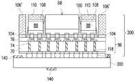
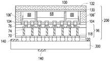
본 명세서에서 논의된 실시형태는, 특정 컨텍스트에서, 즉 패키지 구조물의 휨(warpage)을 줄이기 위해 활성 다이에 인접한 더미 다이 구조물을 포함하는 패키지 구조물에서 논의될 수도 있다. 이러한 패키지 구조물의 휨 감소는 능동 다이와 인터포저 사이의 콜드 조인트(cold joint)의 가능성을 감소시킴으로써 보다 신뢰성있는 패키지 구조물을 가능하게 한다. 일부 실시형태에서, 더미 다이는 스크라이브 라인 영역에 있고, 커버 구조물은 일부 활성 다이를 커버하고, 다른 활성 다이는 커버 구조물로 커버되지 않는다. 더미 다이는 밀봉재의 비율을 더 많이 제어할 수 있으며, 이에 따라 열 팽창 계수(coefficient of thermal expansion; CTE) 불일치로 인한 응력 및 휨을 감소시킬 수도 있다. 일부 실시형태에서, 스크라이브 라인 영역 내의 더미 다이 및/또는 커버 구조물이 패키지 구조물에 대한 충분한 지지 및 보호를 제공하기 때문에, 밀봉재가 생략될 수 있다. 일부 실시형태에서, 활성 다이는 다이 스택의 다른 다이보다 두껍게 되는 다이 스택의 최상부 다이를 가지는 하나 이상의 다이(논리 다이 스택 및/또는 메모리 다이 스택)의 스택이다. 이들 실시형태에서, 스크라이브 라인 영역에서의 더미 다이와 밀봉재는, 상기 다이 스택의 더 두꺼운 상부 다이가 패키지 구조물에 대한 충분한 지지와 보호를 제공하기 때문에 생략될 수 있다.Embodiments discussed herein may be discussed in a particular context, that is, in a package structure that includes a dummy die structure adjacent to the active die to reduce warpage of the package structure. This reduction in package structure allows for a more reliable package structure by reducing the likelihood of cold joints between the active die and the interposer. In some embodiments, the dummy die is in the scribe line area, the cover structure covers some active die, and the other active die is not covered with the cover structure. The dummy die may have more control over the proportion of sealant, thereby reducing stress and warpage due to a coefficient of thermal expansion (CTE) mismatch. In some embodiments, the seal can be omitted because the dummy die and / or cover structure in the scribe line area provides sufficient support and protection for the package structure. In some embodiments, the active die is a stack of one or more dies (logical die stacks and / or memory die stacks) with the top die of the die stack thicker than the other dies in the die stack. In these embodiments, the dummy die and seal in the scribe line area can be omitted because the thicker top die of the die stack provides sufficient support and protection for the package structure.
실시형태는 특정 컨텍스트, 즉 칩-온-웨이퍼-온-기판(Chip-on-Wafer-on-Substrate; CoWoS) 처리를 사용하는 다이-인터포저-기판 적층 패키지와 관련하여 설명될 것이다. 그러나, 다른 실시형태는 다이-다이-기판 적층 패키지와 같은 다른 패키지 및 다른 프로세싱에도 적용될 수 있다. 본 명세서에서 논의된 실시형태들은 본 개시의 주제를 구성하거나 사용할 수 있게 하는 예를 제공하는 것이며, 당업자는 상이한 실시형태의 의도된 범위 내에 유지하면서 행해질 수 있는 변경을 쉽게 이해할 것이다. 아래의 도면에서 동일한 참조 번호와 문자는 동일한 구성요소를 지칭한다. 방법 실시형태가 특정 순서로 수행되는 것으로 논의될 수도 있지만, 다른 방법 실시형태는 임의의 논리적 순서로 수행될 수도 있다.Embodiments will be described in the context of a particular context, a die-interposer-substrate stacking package using Chip-on-Wafer-on-Substrate (CoWoS) processing. However, other embodiments may be applied to other packages and other processing, such as die-die-substrate stacking packages. The embodiments discussed herein provide examples that make up or use the subject matter of the present disclosure, and those skilled in the art will readily appreciate changes that may be made while remaining within the intended scope of different embodiments. In the drawings below, the same reference numerals and letters refer to the same components. Although method embodiments may be discussed as being performed in a particular order, other method embodiments may be performed in any logical order.
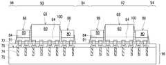
도 1은 일반적으로 하나 이상의 다이(68)의 형성을 예시한다. 기판(60)은 프로세싱 중에 있는 하나 이상의 다이(68)를 포함한다. 실시형태에서의 기판(60)은 웨이퍼이고, 벌크 반도체 기판, 반도체-온-인슐레이터(semiconductor-on-insulator; SOI) 기판, 다층의 반도체 기판 등을 포함할 수도 있다. 일 실시 예에서 기판(60)은 웨이퍼이고 벌크 반도체 기판, SOI(semiconductor-on-insulator) 기판, 다층 반도체 기판 등을 포함할 수도 있다. 기판(60)의 반도체 재료는, 실리콘, 게르마늄, 실리콘 게르마늄, 실리콘 카바이드, 갈륨 비소, 갈륨 인화물, 인듐 인화물, 인듐 비화물 및/또는 인듐 안티몬화물을 포함하는 화합물 반도체; SiGe, GaAsP, AlInAs, AlGaAs, GaInAs, GaInP 및/또는 GaInAsP를 포함하는 합금 반도체; 또는 이들의 조합일 수도 있다. 다층 기판 또는 그래디언트 기판과 같은 다른 기판도 사용될 수있다. 기판(60)은 도핑되거나 도핑되지 않을 수도 있다. 트랜지스터, 커패시터, 저항, 다이오드 등과 같은 디바이스는, 기판(60)의 활성 표면(62) 내에 및/또는 그 활성 표면(62) 상에 형성될 수도 있다. 1 generally illustrates the formation of one or
하나 이상의 유전체 층(들)과 각각의 금속화 패턴(들)을 포함하는 상호 연결 구조물(64)은 활성 표면(62) 상에 형성된다. 유전체 층(들)의 금속화 패턴은, 예를 들어 비아 및/또는 트레이스를 사용하여 디바이스 사이의 전기 신호를 라우팅할 수도 있고, 또한 커패시터, 저항, 인덕터 등과 같은 다양한 전기 디바이스를 포함 할 수도 있다. 다양한 디바이스 및 금속화 패턴은 하나 이상의 기능을 수행하기 위해 상호 연결될 수도 있다. 기능은 메모리 구조물, 프로세싱 구조물, 센서, 증폭기, 전력 분배, 입/출력 회로 등을 포함할 수도 있다. 또한, (예를 들어, 구리와 같은 금속을 포함하는) 도전성 필러(pillar)와 같은 다이 커넥터(66)는 회로 및 디바이스에 외주 전기 접속을 제공하기 위하여 상호 연결 구조물(64) 내에 그리고 상호 연결 구조물(64) 상에 형성된다. 일부 실시형태에서, 다이 커넥터(66)는 상호 연결 구조물(64)로부터 돌출되어 다이(68)를 다른 구조물에 본딩할 때 활용되는 필러 구조물을 형성한다. 당업자는 상기 예들이 예시적인 목적을 위해 제공되어 있다는 것을 인식할 것이다. 다른 회로는 주어진 용도에 알맞게 사용될 수도 있다.An
특히, 상호 금속화 유전체(inter-metallization dielectric; IMD) 층은 상호 연결 구조물(64) 내에 형성될 수도 있다. 상기 IMD 층은, 스피닝, 화학적 기상 증착(CVD), 플라즈마 강화 CVD(PECVD), 고-밀도 플라즈마 화학적 기상 증착(HDP-CVD) 등과 같은 당해 분야에 공지된 임의의 적절한 방법에 의해, 예를 들어, 포스포실리케이트 유리(PSG), 보로포스포실리케이트 유리, 플루오로실리케이트 유리(FSG), SiOXCY, 스핀-온-글라스, 스핀-온-폴리머, 실리콘 탄소 재료, 이들의 화합물, 이들의 복합물, 이들의 조합 등과 같은 로우-K 유전체 재료로 형성될 수도 있다. 금속화 패턴은, 예를 들어 금속화 패턴이 될 수 있는 IMD 층의 부분들을 노출시키기 위해 IMD 층 상에 포토레지스트 재료를 퇴적하고 패터닝하는 포토리소그래피 기술을 이용하여, IMD 층에 형성될 수도 있다. 이방성 건식 에칭 프로세스와 같은 에칭 프로세스는, 상기 IMD 층의 노출된 부분에 대응하는 IMD 층의 리세스 및/또는 개구부를 생성하는데 사용될 수도 있다. 리세스 및/또는 개구부는 확산 배리어 층으로 라인화될 수도 있으며, 도전성 재료로 충전된다. 확산 배리어 층은 원자층 퇴적(ALD) 등에 의해 퇴적된 TaN, Ta, TiN, Ti, CoW 등의 하나 이상의 층을 포함할 수도 있으며, 도전성 재료는 CVD, 물리적 기상 퇴적(PVD) 등에 의해 퇴적된, 구리, 알루미늄, 텅스텐, 은, 및 이들의 조합 등을 포함할 수도 있다. IMD 층 상의 임의의 과도한 확산 배리어 층 및/또는 도전성 재료는 예를 들어 화학적 기계적 연마(CMP)를 사용하여 제거될 수도 있다.In particular, an inter-metallization dielectric (IMD) layer may be formed in
도 2에서, 상호 연결 구조물(64)을 포함하는 기판(60)은 개개의 다이(68)로 싱귤레이팅된다. 일반적으로, 다이(68)는 디바이스 및 금속화 패턴과 같은 동일한 회로를 포함하지만, 다이는 상이한 회로를 가질 수도 있다. 싱귤레이션은 쏘잉(sawing), 다이싱(dicing) 등에 의해 행해질 수도 있다.In FIG. 2, the
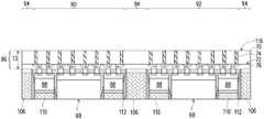
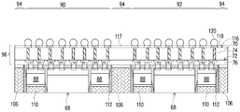
다이(68)는 로직 다이(예를 들어, 중앙 처리 유닛, 그래픽 처리 유닛, 시스템-온-칩, 마이크로컨트롤러 등), 메모리 다이[예를 들어, 동적 랜덤 액세스 메모리(DRAM) 다이, 정적 랜덤 액세스 메모리(SRAM) 다이 등], 무선 주파수(RF) 다이, 센서 다이, MEMS(micro-electro-mechanical-system) 다이, 신호 처리 다이[예를 들어, 디지털 신호 처리(DSP) 다이), 프론트-엔드 다이[예를 들어, 아날로그 프론트-엔드(AFE) 다이) 등, 또는 이들의 조합일 수도 있다. 또한, 일부 실시형태에서, 다이(68)는 상이한 크기(예를 들어, 상이한 높이 및/또는 표면 영역)를 가질 수도 있고, 다른 실시형태에서, 다이(68)는 동일한 크기(예를 들어, 동일한 높이 및/또는 표면 영역)를 가질 수도 있다.
도 3은 하나 이상의 구성요소(96)의 제1 측부의 형성을 예시한다. 도 14에 예시된 바와 같이, 하나 이상의 구성요소(96)는 기판(70)으로부터 형성될 수도 있다. 구성요소(96)가 인터포저 또는 다른 다이일 수도 있다. 기판(70)은 웨이퍼일 수 있다. 기판(70)은 벌크 반도체 기판, SOI 기판, 다층 반도체 기판 등을 포함할 수도 있다. 기판(70)의 반도체 재료는, 실리콘과, 게르마늄과, 실리콘 게르마늄, 실리콘 카바이드, 갈륨 비소, 갈륨 인화물, 인듐 인화물, 인듐 비화물 및/또는 인듐 안티몬화물을 포함하는 화합물 반도체; SiGe, GaAsP, AlInAs, AlGaAs, GaInAs, GaInP, 및/또는 GaInAsP를 포함하는 합금 반도체; 또는 이들의 조합이다. 다층 기판 또는 그래디언트 기판과 같은 다른 기판도 사용될 수 있다. 기판(70)은 도핑되거나 도핑되지 않을 수도 있다. 트랜지스터, 커패시터, 저항, 다이오드 등과 같은 디바이스는, 기판(70)의 활성 표면으로 지칭될 수도 있는 제1 표면(72) 내에 및/또는 그 위에 형성될 수도 있다. 구성요소(96)가 인터포저인 실시형태에서, 비록 인터포저가 제1 표면(72) 내에 및/또는 제1 표면(72) 상에 및/또는 재배선 구조물(76) 내에 형성된 수동 디바이스를 포함할 수도 있다.3 illustrates formation of a first side of one or
관통-비아(through-via; TV)(74)는 기판(70)의 제1 표면(72)으로부터 기판(70)으로 연장되도록 형성된다. TV(74)는 또한 기판(70)이 실리콘 기판일 때 때때로 관통-기판 비아 또는 관통-실리콘 비아로 지칭된다. TV(74)는 예를 들어 에칭, 밀링, 레이저 기술, 이들의 조합 등에 의해 기판(70)에 리세스를 형성함으로써 형성될 수도 있다. 얇은 유전체 재료가, 예를 들어 산화 기술을 사용함으로써, 리세스 내에 형성될 수도 있다. 얇은 배리어 층은 예를 들어 CVD, ALD, PVD, 열 산화, 이들의 조합 등에 의해 기판(70)의 전방 측부 위에 그리고 개구부에 컨포멀하게 퇴적될 수도 있다. 배리어 층은 티타늄 질화물, 티타늄 산질화물, 탄탈륨 질화물, 탄탈륨 산질화물, 텅스텐 질화물, 이들의 조합 등과 같은 질화물 또는 산질화물을 포함할 수도 있다. 도전성 재료는 얇은 배리어 층 위 및 개구부에 퇴적될 수도 있다. 도전성 재료는 전기-화학 도금 프로세스, CVD, ALD, PVD, 이들의 조합 등에 의해 형성될 수도 있다. 도전성 재료의 예는 구리, 텅스텐, 알루미늄, 은, 금, 이들의 조합 등일 수 있다. 과도한 도전성 재료 및 배리어 층은, 예를 들어 CMP에 의해 기판(70)의 전방 측부로부터 제거된다. 이에 따라, TV(74)는 도전성 재료 그리고 도전성 재료와 기판(70) 사이의 얇은 배리어 층을 포함할 수도 있다.A through-via (TV) 74 is formed to extend from the
재배선 구조물(76)은 기판(70)의 제1 표면(72) 상에 형성되고, 만약 있다면, 집적 회로 디바이스 및/또는 TV(74)를 함께 및/또는 외부 디바이스에 전기적으로 연결하는데 사용된다. 재배선 구조물(76)은 유전체 층(들)에 하나 이상의 유전체 층(들) 및 각각의 금속 화 패턴(들)을 포함할 수도 있다. 금속화 패턴은 임의의 디바이스 및/또는 TV(74)를 함께 및/또는 외부 디바이스에 상호 연결하기 위한 비아 및/또는 트레이스를 포함할 수도 있다. 금속화 패턴은 때때로 재배선 라인(Redistribution Line; RDL)으로 지칭된다. 유전체 층은 실리콘 산화물, 실리콘 질화물, 실리콘 탄화물, 실리콘 산질화물과, PSG, BPSG, FSG, SiOxCy, 스핀-온-글라스, 스핀-온-폴리머(Spin-On-Polymer)와 같은 로우-K 유전체 재료, 실리콘 탄소 재료, 이들의 화합물, 이들의 혼합물, 이들의 조합 등을 포함할 수도 있다. 유전체 층은 스피닝, CVD, PECVD, HDP-CVD 등과 같은 당해 분야에 공지된 임의의 적절한 방법에 의해 퇴적될 수도 있다. 금속화 패턴은 예를 들어 포토리소그래피 기술을 사용하여 유전체 층 상에 포토레지스트 재료를 퇴적하고 패터닝하여 금속화 패턴이 될 유전체 층의 부분을 노출시킴으로써 유전체 층에 형성될 수도 있다. 이방성 건식 에칭 프로세스와 같은 에칭 프로세스는, 유전체 층의 노출된 부분에 대응하는 유전체 층에 리세스 및/또는 개구부를 생성하는데 사용될 수도 있다. 리세스 및/또는 개구부는 확산 배리어 층으로 라이닝되고 도전성 재료로 충전될 수도 있다. 확산 배리어 층은 ALD 등에 의해 퇴적된, TaN, Ta, TiN, Ti, CoW 등의 하나 이상의 층을 포함할 수도 있으며, 도전성 재료는, CVD, PVD 등에 의해 퇴적된, 구리, 알루미늄, 텅스텐, 은, 및 이들의 조합 등을 포함할 수도 있다. 유전체 층 상의 임의의 과도한 확산 배리어 층 및/또는 도전성 재료는 예를 들어 CMP를 사용함으로써 제거될 수도 있다.The
전기 커넥터(77/78)는 도전성 패드 상의 재배선 구조물(76)의 상부 표면에 형성된다. 일부 실시형태에서, 도전성 패드는 UBM(under bump metallurgy)을 포함한다. 예시된 실시형태에서, 패드는 재배선 구조물(76)의 유전체 층의 개구부 내에 형성된다. 다른 실시형태에서, 패드(UBM)는 재배선 구조물(76)의 유전체 층의 개구부를 통해 연장될 수 있고, 또한 재배선 구조물(76)의 상부 표면에 걸쳐서 연장될 수도 있다. 패드를 형성하는 예로서, 재배선 구조물(76)의 유전체 층의 적어도 개구부에 시드 층(도시되지 않음)이 형성된다. 일부 실시형태에서, 시드 층은 단일 층 또는 상이한 재료로 형성된 복수의 서브 층을 포함하는 복합 층일 수도 있는 금속 층이다. 일부 실시형태에서, 시드 층은 티타늄 층 및 상기 티타늄 층 위의 구리 층을 포함한다. 시드 층은 예를 들어 PVD 등을 사용하여 형성될 수도 있다. 그 후, 포토레지스트가 시드 층 상에 형성되어 패터닝된다. 포토레지스트는 스핀 코팅 등에 의해 형성될 수도 있고, 패터닝을 위해 광에 노광될 수도 있다. 포토레지스트의 패턴은 패드에 대응한다. 패터닝은 포토레지스트를 통해 개구부를 형성하여 시드 층을 노출시킨다. 도전성 재료는 포토레지스트의 개구부 내에 그리고 시드 층의 노출된 부분 상에 형성된다. 도전성 재료는 전기 도금 또는 무전해 도금 등과 같은 도금에 의해 형성될 수도 있다. 도전성 재료는 구리, 티타늄, 텅스텐, 알루미늄 등과 같은 금속을 포함할 수도 있다. 그 후, 포토레지스트, 및 시드 층 중 도전성 재료가 형성되지 않은 부분을 제거한다. 포토레지스트는 허용 가능한 애싱(ashing) 또는 스트립핑(stripping) 프로세스, 예를 들어 산소 플라즈마 등을 사용함으로써 제거될 수도 있다. 일단 포토레지스트가 제거되면, 예를 들어 습식 또는 건식 에칭과 같은 허용 가능한 에칭 프로세스를 사용함으로써, 시드 층의 노출 된 부분이 제거된다. 시드 층 및 도전성 재료의 나머지 부분은 패드를 형성한다. 패드가 다르게 형성되는 실시형태에서는, 보다 많은 포토 레지스트 및 패터닝 단계가 이용될 수도 있다.
일부 실시형태에서, 전기 커넥터(77/78)는 금속 필러(77) 위에, 땜납 캡(78)일 수도 있는 금속 캡 층(78)을 구비하는 금속 필러(77)을 포함한다. 상기 필러(77) 및 상기 캡 층(78)을 포함하는 전기 커넥터(77/78)는 때때로 마이크로 범프(77/78)로 지칭된다. 일부 실시형태에서, 금속 필러(77)는 구리, 알루미늄, 금, 니켈, 팔라듐 등, 또는 이들의 조합과 같은 도전성 재료를 포함하며, 스퍼터링, 인쇄, 전기 도금, 무전해 도금, CVD 등에 의해 형성될 수도 있다. 금속 필러(77)는 솔더 프리(solder free)일 수도 있고, 실질적으로 수직의 측벽을 갖는다. 일부 실시형태에서, 금속 캡 층(78)은 금속 필러(77)의 상부에 형성된다. 금속 캡 층(78)은 니켈, 주석, 주석-납, 금, 구리, 은, 팔라듐, 인듐, 니켈-팔라듐-금, 니켈-금 등, 또는 이들의 조합을 포함할 수도 있고, 도금 프로세스에 의해 형성될 수도 있다.In some embodiments,
다른 실시형태에서, 전기 커넥터(77/78)는 금속 필러를 포함하지 않고, 제어된 붕괴 칩 연결부(controlled collapse chip connection; C4), 무전해 니켈 침지 금(electroless nickel immersion Gold; ENIG), 무전해 니켈 무전해 팔라듐 침지 금(electroless nickel electroless palladium immersion gold; ENEPIG) 기법으로 형성된 범프 등과 같은, 땜납 볼 및/또는 범프이다. 이 실시형태에서, 범프 전기 커넥터(77/78)는 땜납, 구리, 알루미늄, 금, 니켈, 은, 팔라듐, 주석 등, 또는 이들의 조합과 같은 도전성 재료를 포함할 수도 있다. 이 실시형태에서, 전기 커넥터(77/78)는 증발, 전기 도금, 인쇄, 솔더 이송, 볼 배치 등과 같은 일반적으로 사용되는 방법을 통해 초기에 땜납 층을 형성함으로써 형성된다. 일단 구조물 상에 땜납 층이 형성되어 있으면, 재료를 원하는 범프 형상으로 성형하기 위해 리플 로우가 수행될 수도 있다.In another embodiment, the
도 4에서, 다이(68) 및 다이(88)는 예를 들어 전기 커넥터(77/78) 및 다이 상의 금속 필러(79)에 의한 플립 칩 본딩을 통해, 구성요소(96)의 제1 측부에 부착되어, 도전성 조인트(91)를 형성한다. 금속 필러(79)는 금속 필러(77)와 유사할 수도 있으며, 이에 대한 설명이 본 명세서에서는 반복되지 않는다. 다이(68) 및 다이(88)는 예를 들어 픽-앤드-플레이스(pick-and-place) 툴을 사용하여 전기 커넥터(77/78) 상에 배치될 수도 있다. 일부 실시형태에서, 금속 캡 층(78)은 (도 3에 도시된 바와 같이) 금속 필러(77) 상에, 다이(68) 및 다이(88)의 금속 필러(79) 상에, 또는 양자 모두에 형성된다.In FIG. 4, die 68 and die 88 are provided on the first side of
다이(88)는 다이(68)와 관련하여 전술한 바와 유사한 프로세싱을 통해 형성될 수도 있다. 일부 실시형태에서, 다이(88)는 메모리 다이(예를 들어, DRAM 다이, SRAM 다이, 고대역폭 메모리(High-Bandwidth Memory; HBM) 다이, 하이브리드 메모리 큐브(Hybrid Memory Cube; HMC) 다이 등)의 스택과 같은 하나 이상의 메모리 다이를 포함한다. 메모리 다이 실시형태의 스택에서, 다이(88)는 예를 들어 메모리 제어기를 갖는 4개 또는 8개의 메모리 다이의 스택과 같은, 메모리 다이 및 메모리 컨트롤러 모두를 포함할 수도 있다. 또한, 일부 실시형태에서, 다이(88)는 상이한 크기(예를 들어, 상이한 높이 및/또는 표면 영역)를 가질 수도 있고, 다른 실시형태에서, 다이(88)는 동일한 크기(예를 들어, 동일한 높이 및/또는 표면 영역)를 가질 수도 있다.
다이(88)는 본체(80), 상호 연결 구조물(84), 및 다이 커넥터(86)를 포함한다. 다이(88)의 본체(80)는 임의의 개수의 다이, 기판, 트랜지스터, 능동 디바이스, 수동 디바이스 등을 포함할 수도 있다. 일 실시형태에서, 본체(80)는 벌크 반도체 기판, SOI(semiconductor-on-insulator) 기판, 다층 반도체 기판 등을 포함할 수도 있다. 본체(80)의 반도체 재료는 실리콘과, 게르마늄과, 실리콘 게르마늄, 실리콘 탄화물, 갈륨 비소, 갈륨 인화물, 인듐 인화물, 인듐 비화물 및/또는 인듐 안티몬화물을 포함하는 화합물 반도체; SiGe, GaAsP, AlInAs, AlGaAs, GaInAs, GaInP, 및/또는 GaInAsP를 포함하는 합금 반도체; 또는 이들의 조합일 수도 있다. 다층 기판 또는 그래디언트 기판과 같은 다른 기판도 사용될 수도 있다. 본체(80)는 도핑되거나 도핑되지 않을 수도 있다. 트랜지스터, 커패시터, 저항, 다이오드 등과 같은 디바이스는 능동 표면에 및/또는 능동 표면 상에 형성될 수도 있다.
하나 이상의 유전체 층(들) 및 각각의 금속화 패턴(들)을 포함하는 상호 연결 구조물(84)이 활성 표면 상에 형성된다. 유전체 층(들) 내의 금속화 패턴(들)은 예를 들어 비아 및/또는 트레이스를 사용함으로써 디바이스들 사이에서 전기 신호들을 라우팅할 수도 있고, 또한 커패시터, 저항, 인덕터 등과 같은 다양한 전기 디바이스를 포함할 수도 있다. 다양한 디바이스 및 금속화 패턴은 하나 이상의 기능을 수행하도록 상호 연결될 수도 있다. 기능은 메모리 구조물, 프로세싱 구조물, 센서, 증폭기, 전력 분배, 입/출력 회로 등을 포함할 수도 있다. 부가적으로, (예를 들어, 구리와 같은 금속을 포함하는) 도전성 필러와 같은 다이 커넥터(86)가 상호 연결 구조물(84) 내에 및/또는 그 위에 형성되어 회로 및 디바이스에 외부 전기 접속을 제공한다. 일부 실시형태에서, 다이 커넥터(86)는 상호 연결 구조물(84)로부터 돌출하여, 다이(88)를 다른 구조물에 본딩할 때 활용되는 필러 구조물을 형성한다. 당업자는 상기 예가 설명의 목적으로 제공된다는 것을 인식할 것이다. 다른 회로가 주어진 애플리케이션에 적절하게 사용될 수도 있다.An
더욱 구체적으로, 상호연결 구조물(64)에 IMD 층이 형성될 수도 있다. IMD 층은, 스피닝, CVD, PECVD, HDP-CVD 등과 같은 당해 분야에 알려진 임의의 적절한 방법에 의해, 예를 들어 PSG, BPSG, FSG, SiOxCy, 스핀-온-글라스, 스핀-온-폴리머, 실리콘 탄소 재료, 이들의 화합물, 이들의 복합물, 이들의 조합 등과 같은 로우-K 유전체 재료로 형성될 수도 있다. 금속화 패턴은 예를 들어 포토리소그래피 기술을 이용하여 IMD 층 상에 포토레지스트 재료를 퇴적하고 패터닝하여 금속화 패턴이 될 IMD 층의 부분을 노출시킴으로써, IMD 층에 형성될 수도 있다. 이방성 건식 에칭 프로세스와 같은 에칭 프로세스는, IMD 층의 노출된 부분에 대응하는 IMD 층에 리세스 및/또는 개구부를 생성하는데 사용될 수도 있다. 리세스 및/또는 개구부는 확산 배리어 층으로 라이닝되고 도전성 재료로 충전될 수도 있다. 확산 배리어 층은 ALD 등에 의해 퇴적된, 탄탈륨 질화물, 탄탈륨, 티타늄 질화물, 티타늄, 코발트 텅스텐 등, 또는 이들의 조합의 하나 이상의 층을 포함할 수도 있다. 금속화 패턴의 도전성 재료는, CVD, PVD 등에 의해 퇴적된, 구리, 알루미늄, 텅스텐, 은, 및 이들의 조합 등을 포함할 수도 있다. IMD 층 상의 임의의 과도한 확산 배리어 층 및/또는 도전성 재료는 예를 들어 CMP를 사용함으로써 제거될 수도 있다.More specifically, an IMD layer may be formed in the
다이 커넥터(66 및 86)가 상호 연결 구조물(64 및 84)로부터 각각 돌출하는 실시형태에서, 돌출 다이 커넥터(66 및 86)가 금속 캡 층(78)에 대한 필러로서 사용될 수도 있기 때문에, 금속 필러(79)는 다이(68 및 88)로부터 제외될 수도 있다.In embodiments in which the
도전성 조인트(91)는 다이(68) 및 다이(88)의 회로를 상호 연결 구조물(84 및 64) 및 다이 커넥터(86 및 66)를 통해 각각 구성요소(96) 내의 재배선 구조물(76) 및 TV(74)에 전기적으로 연결한다.Conductive joint 91 connects circuitry of
일부 실시형태에서, 전기 커넥터(77/78)를 본딩하기 전에, 전기 커넥터(77/78)는 무세정 플럭스와 같은 플럭스(미도시)로 코팅된다. 전기 커넥터(77/78)는 플럭스 내에 침지될 수도 있거나, 또는 플럭스가 전기 커넥터(77/78) 상으로 분사될 수도 있다. 다른 실시형태에서, 플럭스는 전기 커넥터(79/78)에 인가될 수도 있다. 일부 실시형태에서, 전기 커넥터(77/78 및 79/78)는, 다이(68) 및 다이(88)가 구성요소(96)에 부착된 이후에 남아있는 에폭시 플럭스의 에폭시 부분의 적어도 일부로 리플로우되기 전에 상기 커넥터 위에 형성된 에폭시 플럭스(도시되지 않음)를 가질 수도 있다. 이러한 잔여 에폭시 부분은 응력을 감소시키고 전기 커넥터(77/78/79)의 리플로우로 인해 발생하는 조인트를 보호하기 위한 언더필(underfill)로서 기능할 수도 있다.In some embodiments, prior to bonding
다이(68 및 88)와 구성요소(96) 사이의 본딩은 땜납 본딩 또는 직접 금속 대 금속(예를 들어, 구리 대 구리 또는 주석 대 주석) 본딩일 수도 있다. 일 실시형태에서, 다이(68) 및 다이(88)는 리플로우 프로세스에 의해 구성요소(96)에 본딩된다. 이러한 리플로우 프로세스 동안에, 전기 커넥터(77/78/79)는, 다이(68) 및 다이(88)를 구성요소(96)에 물리적으로 그리고 전기적으로 연결하기 위해, 각각 다이 커넥터(66 및 86)와 재배선 구조물(76)의 패드와 접촉한다. 본딩 프로세스 후에, 금속 필러(77, 79)와 금속 캡 층(78)의 계면에 IMC(도시되지 않음)가 형성될 수도 있다.Bonding between dies 68 and 88 and
도 4 및 후속하는 도면에서, 각각 제1 패키지 및 제2 패키지의 형성을 위한 제1 패키지 영역(90) 및 제2 패키지 영역(92)이 예시된다. 스크라이브 라인 영역(94)은 인접한 패키지 영역 사이에 있다. 도 4에 예시된 바와 같이, 다이(68) 및 복수의 다이(88)가 제1 패키지 영역(90) 및 제2 패키지 영역(92)의 각각에 부착된다.In FIG. 4 and the subsequent figures, a
일부 실시형태에서, 다이(68)는 시스템-온-칩(SoC) 또는 그래픽 처리 유닛(GPU)이고, 제2 다이는 다이(68)에 의해 활용될 수도 있는 메모리 다이이다. 일 실시형태에서, 다이(88)는 적층된 메모리 다이이다. 예를 들어, 적층된 메모리 다이(88)는 LPDDR1, LPDDR2, LPDDR3, LPDDR4, 또는 유사한 메모리 모듈과 같은 저전력(low-power; LP) 이중 데이터 레이트(double data rate; DDR) 메모리 모듈을 포함할 수도 있다.In some embodiments, die 68 is a system-on-chip (SoC) or graphics processing unit (GPU) and the second die is a memory die that may be utilized by
도 5에서, 언더필 재료(100)는 다이(68), 다이(88), 재배선 구조물(76) 사이에 있으며 도전성 조인트(91)를 둘러싸는 갭에 제공된다. 도 5 및 후속하는 도면들에서, 각각의 도전성 조인트(91)의 예시는 단일 구조물을 포함하는 것으로 도시되어 있지만, 도 4에 예시된 바와 같이, 각각의 도전성 조인트(91)는 금속 층(78)을 사이에 구비하는 2개의 금속 필러(77 및 79)를 포함할 수 있다. 언더필 재료(100)는 다이(68) 및 다이(88)의 측벽을 따라 위로 연장될 수도 있다. 언더필 재료(100)는 폴리머, 에폭시, 몰딩 언더필 등과 같은 임의의 허용 가능한 재료일 수도 있다. 언더필 재료(100)는 다이(68 및 88)가 부착된 후에 모세관 유동 프로세스에 의해 형성될 수 있거나, 다이(68 및 88)가 부착되기 전에 적절한 퇴적 방법에 의해 형성될 수도 있다.In FIG. 5,
도 6a 및 도 6b에서, 더미 다이(106)는 부착 구조물(104)에 의해 다이(88)에 인접한 스크라이브 라인 영역(94)에 부착된다. 도 6a 및 도 6b는 부착 구조물(104)에 대한 2개의 실시형태를 예시한다. 스크라이브 라인 영역(94)에 배치되는 더미 다이(106)는 제1 및 제2 패키지 영역(90 및 92) 내의 패키지들의 싱귤레이션 동안 및 그 이후(도 14 참조)의 휨을 방지하는 것을 도울 수 있다. 더미 다이(106)가 휨을 감소시키는 것을 도울 수 있는 하나의 방법은 실제 싱귤레이션 프로세스 동안에 패키지를 지지하는 것이다. 더미 다이(106)가 휨을 방지할 수 있는 또 다른 방법은, 더미 다이(106)가 구성요소(96)와 유사한 열팽창 계수(coefficient of thermal expansion; CTE)를 가지며, 상기 더미 다이가 패키지에 필요한 밀봉재(112)의 양을 감소시키기 때문에, 만일 존재하는 경우(도 8을 참조), 구성 요소(96)와 후속하여 형성된 밀봉재(112) 사이의 열팽창 계수(CTE) 불일치를 감소시키는 것이다.6A and 6B, dummy die 106 is attached to
더미 다이(106)는 부착 구조물(104)에 의해 구성요소(96)에 부착된다. 일부 실시형태에서, 부착 구조물(104)은 더미 다이(106)를 구성요소에 본딩하는 하나 이상의 마이크로 범프이다. 일부 실시형태에서, 부착 구조물(104)는 더미 다이(106)를 구성요소(96)에 부착시키는 접착제이다. 더미 다이(106)는 실리콘, 유전체 재료 등, 또는 이들의 조합으로 제조될 수도 있다. 일부 실시형태에서, 더미 다이(106)는 실제로 더미 다이(106)로서 재활용된 결함있는 활성 다이이다. 일부 실시형태에서, 더미 다이(106)는 벌크 재료이고 임의의 능동 또는 수동 디바이스를 포함하지 않는다. 일부 실시형태에서, 더미 다이(106)의 상부 표면은 다이(68)의 후방 측부와 동일한 높이를 가진다.The dummy die 106 is attached to the
도 6a에는, 마이크로 범프 부착 구조물(104)의 실시형태가 예시되어 있다. 이 실시형태에서, 마이크로 범프(104)는 더미 다이(106)의 바닥 표면, 구성요소(96)의 상부 표면, 또는 양자 모두에 형성된다. 마이크로 범프(104)는 다이(68, 88)를 본딩하는 마이크로 범프[예를 들어, 전기 커넥터(77/78/79)]와 동시에 형성될 수 있다. 특히, 부착 구조물(104)의 구조물(104A, 104B, 및 104C)는 각각 구조물(77, 78, 및 79)과 동일할 수 있으며, 이들 구조물에 대한 설명은 본 명세서에서는 반복하지 않는다. 마이크로 범프(104)는 도면에서 재배선 구조물(76)과 같은 구성 요소(96)에 더미 다이(106)를 본딩한다. 더미 다이(106)의 마이크로 범프(104)는 다이(68 및 88)의 전기 커넥터(77/78/79)와 함께 리플로우될 수 있다. 더미 다이(106)는 예를 들어 픽-앤-플레이스 툴을 사용하여 마이크로 범프(104) 상에 배치될 수도 있다. 언더필 재료(100)는 더미 다이(106)가 본딩되기 전 또는 본딩된 후에 경화될 수 있다.6A, an embodiment of a micro
도 6b에는, 접착제 부착 구조물(104)의 실시형태가 예시되어 있다. 이 실시형태에서, 접착제(104)는 더미 다이(106)의 바닥 표면 상에 존재하고, 도면에서 재배선 구조물(76)과 같은 구성요소(96)에 더미 다이(106)를 부착한다. 접착제(104)는 임의의 적절한 접착제, 에폭시, 다이 부착 필름(die attach film; DAF) 등일 수도 있다. 접착제(104)는 더미 다이(106)의 바닥 표면에 도포되거나, 재배선 구조물(76)의 표면 위에 도포될 수도 있다. 더미 다이(106)는 예를 들어 픽-앤드-플레이스 툴을 사용하여 접착제(104)에 의해 재배선 구조물(76)에 부착될 수도 있다. 언더필 재료(100)는 더미 다이(106)가 부착되기 전 또는 부착된 후에 경화될 수 있다.In FIG. 6B, an embodiment of an
도 7에서, 커버 구조물(110)은 다이(88)의 후방 측부에 부착된다. 커버 구조물(110)은 다이(88)에 가해지는 응력을 현저하게 감소시키고 후속 프로세싱 동안에 다이(88)를 보호할 수 있다. 일부 실시형태에서, 다이(88)는 하나 이상의 메모리 다이의 스택을 포함하고, 커버 구조물(110)은 다이(88)의 하나 이상의 메모리 다이의 각각보다 두껍다. 일부 실시형태에서, 커버 구조물(110)은 약 100 ㎛와 같은, 약 50 ㎛ 내지 약 200 ㎛의 범위에서 기판(70)의 주 표면에 수직한 방향으로 측정된 두께를 갖는다.In FIG. 7,
일부 실시형태에서, 커버 구조물(110)의 상부 표면은, 다이(68)의 후방 측부 및 더미 다이(106)의 상부 표면과 동일한 높이를 가진다. 일부 실시형태에서, 커버 구조물(110)은 접착제(108)로 부착된다. 커버 구조물(110)는 실리콘, 유전체 재료 등, 또는 이들의 조합으로 제조될 수도 있다. 커버 구조물(110)은 더미 다이(106)와 동일한 재료를 포함할 수도 있다. 일부 실시형태에서, 커버 구조물(110)은 실제로 커버 구조물(110)로서 재활용된 결함있는 활성 다이이다. 일부 실시형태에서, 커버 구조물(110)은 벌크 재료이고 임의의 능동 또는 수동 디바이스를 포함하지 않는다. 접착제(108)는 커버 구조물(110)의 바닥 표면에 있고 커버 구조물(110)를 다이(88)에 부착시킨다. 접착제(108)는 임의의 적절한 접착제, 에폭시, DAF 등일 수도 있다. 커버 구조물(110)은 예를 들어 픽-앤드-플레이스 툴을 사용하여 접착제(108)에 의해 다이(88)에 부착될 수도 있다.In some embodiments, the top surface of
도 8에서, 밀봉재(112)는 다양한 구성요소 상에 형성된다. 밀봉재(112)는 몰딩 화합물, 에폭시 등일 수도 있으며, 압축 몰딩, 트랜스퍼 몰딩 등에 의해 도포될 수도 있다. 밀봉재(112)를 경화시키기 위한 경화 단계가 수행되며, 여기서 경화는 열 경화, 자외선(Ultra-Violet; UV) 경화 등일 수도 있다. 일부 실시형태에서, 다이(68), 더미 다이(106) 및/또는 커버 구조물(110)는 밀봉재(112) 내에 매립되고, 밀봉재(112)의 경화 후에, 연마와 같은 평탄화 단계가 수행되어 밀봉재(112)의 잉여 부분을 제거하며, 상기 잉여 부분은 다이(68), 더미 다이(106), 및/또는 커버 구조물(110)의 상부 표면 위에 있다. 따라서, 다이(68), 더미 다이(106) 및/또는 커버 구조물(110)의 상부 표면은 노출되고, 밀봉재(112)의 상부 표면과 동일한 높이를 가진다.In FIG. 8, the
도 9 내지 도 12는 구성요소(96)의 제2 측부의 형성을 예시한다. 도 9에서, 도 8의 구조물을 뒤집어 구성요소(96)의 제2 측부의 형성을 준비한다. 도시되지는 않았지만, 구조물은 도 9 내지 도 12의 프로세스를 위한 캐리어 또는 지지 구조물 상에 배치될 수도 있다. 도 9에 도시된 바와 같이, 이 프로세싱 단계에서, 구성요소(96)의 기판(70) 및 재배선 구조물(76)은 약 775 ㎛와 같은, 약 750 ㎛ 내지 약 800 ㎛의 범위의 조합된 두께(T1)를 갖는다. 더미 다이(106)[부착 구조물(104)를 포함함]는 약 760 ㎛와 같은, 약 750 ㎛ 내지 약 800 ㎛의 범위의 두께(T2)를 갖는다. 일부 실시형태에서, 다이(68 및 88)[다이(88)에 대한 도전성 조인트(91) 및 커버 구조물(110)을 포함함] 중 하나 또는 양자 모두는 두께(T2)를 갖는다.9-12 illustrate the formation of the second side of
도 10에서, TV(74)가 노출될 때 까지, 기판(70)을 제2 표면(116)으로 까지 얇게 하기 위하여 기판(70)의 제2 측부에 대해 박화 프로세스가 수행된다. 박화 프로세스는 에칭 프로세스, 연마 프로세스 등, 또는 이들의 조합을 포함할 수도 있다. 일부 실시형태에서, 박화 프로세스 후에, 구성요소(96)의 기판(70) 및 재배선 구조물(76)은 약 100 ㎛와 같은, 약 20 ㎛ 내지 약 180 ㎛의 범위의 조합된 두께(T3)를 갖는다.In FIG. 10, a thinning process is performed on the second side of the
도 11에서, 재배선 구조물은 기판(70)의 제2 표면(116) 상에 형성되고, TV(74)를 함께 및/또는 외부 디바이스에 전기적으로 연결하는데 사용된다. 재배선 구조물은 하나 이상의 유전체 층(117) 및 상기 하나 이상의 유전체 층(117) 내의 금속화 패턴(118)을 포함한다. 금속화 패턴은 TV(74)를 함께 및/또는 외부 디바이스에 상호 연결하기 위한 비아 및/또는 트레이스를 포함할 수도 있다. 금속화 패턴(118)은 때때로 재배선 라인(Redistribution Line; RDL)으로 지칭된다. 유전체 층(117)은, 실리콘 산화물과, 실리콘 질화물과, 실리콘 탄화물과, 실리콘 산질화물과, PSG, BPSG, FSG, SiOxCy, 스핀-온-글라스, 스핀-온-폴리머와 같은 로우-K 유전체 재료, 실리콘 탄소 재료, 이들의 화합물, 이들의 복합물, 이들의 조합 등을 포함할 수도 있다. 유전체 층 (117)은 스피닝, CVD, PECVD, HDP-CVD 등과 같은 당해 분야에 알려진 임의의 적절한 방법에 의해 퇴적될 수도 있다. 금속화 패턴(118)은, 예를 들어 포토리소그래피 기술을 사용하여 유전체 층(117) 상에 포토레지스트 재료를 퇴적하고 패터닝하여 금속화 패턴(118)이 될 유전체 층(117)의 부분을 노출시킴으로써, 유전체 층(117)에 형성될 수도 있다. 이방성 건식 에칭 프로세스와 같은 에칭 프로세스는, 유전체 층(117)의 노출된 부분에 대응하는 유전체 층(117) 내에 리세스 및/또는 개구부를 생성하는데 사용될 수도 있다. 리세스 및/또는 개구부는 확산 배리어 층으로 라이닝되고 도전성 재료로 충전될 수도 있다. 확산 배리어 층은 ALD 등에 의해 퇴적된, TaN, Ta, TiN, Ti, CoW 등의 하나 이상의 층을 포함할 수도 있으며, 도전성 재료는 CVD, PVC 등에 의해 퇴적된, 구리, 알루미늄, 텅스텐, 은, 및 이들의 조합 등을 포함할 수도 있다. 유전체 층 상의 임의의 과도한 확산 배리어 층 및/또는 도전성 재료는, 예를 들어 CMP를 사용함으로써 제거될 수도 있다.In FIG. 11, the redistribution structure is formed on the
도 12에서, 전기 커넥터(120)는 또한 금속화 패턴(118) 상에 형성되고, TV(74)에 전기적으로 연결된다. 전기 커넥터(120)는 금속화 패턴(118) 상의 재배선 구조물의 상부 표면에 형성된다. 일부 실시형태에서, 금속화 패턴(118)은 UBM을 포함한다. 예시된 실시형태에서, 패드는 재배선 구조물의 유전체 층(117)의 개구부 내에 형성된다. 다른 실시 형태에서, 패드(UBM)는 재배선 구조물의 유전체 층(117)의 개구부를 통해 연장될 수 있고, 또한 재배선 구조물의 상부 표면에 걸쳐서 연장될 수 있다.In FIG. 12,
패드를 형성하는 예로서, 재배선 구조물의 유전체 층(117) 중 하나의 유전체 층의 개구부에 적어도 시드 층(도시하지 않음)이 형성된다. 일부 실시형태에서, 시드 층은 금속 층이며, 이 금속 층은 단일 층 또는 상이한 재료로 형성된 복수의 서브 층을 포함하는 복합 층일 수 있다. 일부 실시형태에서, 시드 층은 티타늄 층 및 이 티타늄 층 위의 구리 층을 포함한다. 시드 층은 예를 들어 PVD 등을 사용하여 형성될 수도 있다. 그 후, 포토레지스트가 시드 층 상에 형성되어 패터닝된다. 포토레지스트는 스핀 코팅 등에 의해 형성될 수도 있고, 패터닝을 위해 광에 노광될 수도 있다. 포토레지스트의 패턴은 패드에 대응한다. 패터닝은 포토레지스트를 통해 개구부를 형성하여 시드 층을 노출시킨다. 도전성 재료가 포토레지스트의 개구부 내에 그리고 시드 층의 노출 된 부분 상에 형성된다. 도전성 재료는 전기 도금 또는 무전해 도금 등과 같은 도금에 의해 형성될 수도 있다. 도전성 재료는 구리, 티타늄, 텅스텐, 알루미늄 등과 같은 금속을 포함할 수도 있다. 그 후, 포토레지스트 및 시드 층 중 도전성 재료가 형성되어 있지 않은 부분을 제거한다. 포토레지스트는 허용 가능한 애싱 또는 스트립핑 프로세스에 의해, 예컨대 산소 플라즈마 등을 사용하여 제거될 수도 있다. 일단 포토레지스트가 제거되면, 예를 들어 습식 또는 건식 에칭과 같은 허용 가능한 에칭 프로세스를 사용함으로써, 시드 층의 노출된 부분이 제거된다. 시드 층 및 도전성 재료의 나머지 부분은 패드를 형성한다. 패드가 다르게 형성되는 실시형태에서, 보다 많은 포토레지스트 및 패터닝 단계가 활용될 수도 있다.As an example of forming the pad, at least a seed layer (not shown) is formed in an opening of one of the
일부 실시형태에서, 전기 커넥터(120)는 볼 그리드 어레이(ball grid array; BGA) 볼, C4 마이크로 범프, ENIG 형성 범프, ENEPIG 형성 범프 등과 같은, 땜납 볼 및/또는 범프이다. 전기 커넥터(120)는 땜납, 구리, 알루미늄, 금, 니켈, 은, 팔라듐, 주석 등, 또는 이들의 조합과 같은 도전성 재료를 포함할 수도 있다. 일부 실시형태에서, 전기 커넥터(120)는 증발, 전기 도금, 인쇄, 납땜 이송, 볼 배치 등과 같은 이러한 일반적으로 사용되는 방법을 통해 초기에 땜납 층을 형성함으로써 형성된다. 일단 구조물 상에 땜납 층이 형성되면, 재료를 원하는 범프 형상으로 성형하기 위하여 리플로우가 수행될 수도 있다. 다른 실시형태에서, 전기 커넥터(120)는 스퍼터링, 인쇄, 전기 도금, 무전해 도금, CVD 등에 의해 형성된 금속 필러(예를 들어, 구리 필러)이다. 상기 금속 필러는 솔더 프리일 수도 있고, 실질적으로 수직의 측벽을 가질 수도 있다. 일부 실시형태에서, 금속 필러 커넥터(120)의 상부에 금속 캡 층(도시되지 않음)이 형성된다. 금속 캡 층은 니켈, 주석, 주석-납, 금, 은, 팔라듐, 인듐, 니켈-팔라듐-금, 니켈-금 등, 또는 이들의 조합을 포함할 수도 있고, 도금 프로세스에 의해 형성될 수도 있다.In some embodiments,
전기 커넥터(120)는 추가적인 전기 구성요소에 본딩하는데 사용될 수도 있고, 이러한 추가적인 전기 구성요소는 반도체 기판, 패키지 기판, 인쇄 회로 기판(Printed Circuit Board; PCB) 등(도 15의 300 참조)일 수 있다.The
도 13은 도 12의 패키지 구조의 평면도를 예시한다. 도 12는 도 13의 라인 A-A를 따른 단면도이다. 도 13에 예시된 바와 같이, 더미 다이(106)는 각각의 패키지 영역(90 및 92)을 둘러싸는 스크라이브 라인 영역(94)을 따라 존재한다.FIG. 13 illustrates a top view of the package structure of FIG. 12. 12 is a cross-sectional view along the line A-A of FIG. 13. As illustrated in FIG. 13, dummy die 106 is present along
일부 실시형태에서, 더미 다이(106)는 스크라이브 라인 영역(94)에 부착되고, 제1 방향(예를 들어, 도 13의 수직 방향)을 따르는 스크라이브 라인 영역(94)만을 따라 연장된다. 일부 실시형태에서, 패키지 구조물은 3개 이상의 다이(88)를 가질 수 있고(예를 들어, 4 개의 다이(88)를 가질 수 있음), 패키지 구조물은 동일한 영역(90 및/또는 92)의 인접한 다이(88) 사이에 삽입된 더 많은 더미 다이(122)를 가질 수 있다. 더미 다이(122)는 더미 다이(106)와 유사하므로, 본 명세서에서는 설명을 반복하지 않는다.In some embodiments, dummy die 106 is attached to
또한, 일부 실시 예에서, 더미 다이(106)는 스크라이브 라인 영역(94)에 부착되고, 제1 방향 및 제2 방향(예를 들어, 도 13의 수직 및 수평 방향 모두)을 따르는 스크라이브 라인 영역을 따라 연장되며, 또한 동일한 영역(90 및/또는 92)의 인접한 다이(88) 사이에 삽입된다.Further, in some embodiments, the dummy die 106 is attached to the
도 13이 싱귤레이션 이후에 4개의 패키지 구조물을 형성하는 웨이퍼의 4개의 영역을 도시하지만, 본 개시는 이러한 영역 및 패키지 구조물의 양으로 제한되지 않는다. 다른 실시형태에서, 본 개시는 더 많거나 더 적은 영역 및 패키지 구조물을 포함할 수도 있다.Although FIG. 13 illustrates four regions of a wafer forming four package structures after singulation, the present disclosure is not limited to the amount of such regions and package structures. In other embodiments, the present disclosure may include more or fewer regions and package structures.
도 14에서, 특히 다이(68), 구성요소(96), 다이(88), 커버 구조물(110), 더미 다이(106)의 부분(106’)을 구비하는 구성요소 패키지(200)를 형성하기 위하여, 스크라이브 라인 영역(94)을 따라 인접한 영역(90 및 92) 사이에 구성요소(96) 및 더미 다이(106)가 싱귤레이트된다. 싱귤레이션은 쏘잉, 다이싱 등에 의해 행해질 수도 있다. 전술한 바와 같이, 더미 다이(106)는 싱귤레이션 프로세스 동안에 그리고 그 이후에 야기되는 응력 및 휨을 감소시키는 것을 돕는다.In FIG. 14, in particular, forming
싱귤레이션 프로세스 이후에, 더미 다이(106)의 나머지 부분(106’)은 구성요소 패키지(200)의 측면 범위와 접하는 측벽 표면을 갖는다(예를 들어, 도 14 및 도 15 참조).After the singulation process, the remaining portion 106 'of the dummy die 106 has a sidewall surface that abuts the lateral extent of the component package 200 (see, for example, FIGS. 14 and 15).
도 15는 기판(300) 상의 컴포넌트 패키지(200)의 부착을 예시한다. 전기 커넥터(120)는 기판(300)의 본드 패드와 정렬되어 배치된다. 전기 커넥터(120)는 리플로우되어 기판(300)과 구성요소(96) 사이에 본드를 생성할 수도 있다. 기판(300)은 내부에 코어를 포함하는 빌드-업 기판과 같은 패키지 기판, 복수의 적층된 유전체 막을 포함하는 라미네이트 기판, PCB 등을 포함할 수도 있다. 기판(300)은 기판(300)이 다른 디바이스에 장착될 수 있도록 구성요소 패키지에 대향하는 땜납 볼과 같은 전기 커넥터(도시되지 않음)를 포함할 수도 있다. 언더필 재료(도시되지 않음)는 전기 커넥터(120)를 둘러싸면서, 구성요소 패키지(200)와 기판(300) 사이에 배치될 수 있다. 언더필 재료는 폴리머, 에폭시, 몰딩 언더필 등과 같은 임의의 허용 가능한 재료일 수도 있다.15 illustrates the attachment of the
또한, 하나 이상의 표면 디바이스(140)가 기판(300)에 연결될 수도 있다. 표면 디바이스(140)는 구성요소 패키지(200) 또는 패키지 전체에 추가적인 기능 또는 프로그래밍을 제공하는데 사용될 수도 있다. 일 실시형태에서, 표면 디바이스(140)는, 구성요소 패키지(200), 또는 그 패키지의 다른 부분에 연결되고 이들과 함께 활용되도록 희망하는, 저항, 인덕터, 커패시터, 점퍼, 이들의 조합 등과 같은 수동 디바이스를 포함하는 표면 실장 디바이스(surface mount device; SMD) 또는 집적 수동 디바이스(integrated passive device; IPD)를 포함할 수도 있다. 표면 디바이스(140)는 다양한 실시형태에 따라, 기판(300)의 제1 주 표면, 기판(300)의 대향하는 주 표면, 또는 양자 모두에 배치될 수도 있다.In addition, one or
도 16은 일부 실시형태에 따른 패키지 구조물의 단면도를 예시한다. 도 16의 실시형태는 도 16이 밀봉재(112)를 포함하지 않는다는 점을 제외하고는 도 1 내지 도 15의 실시형태와 유사하다. 더미 다이(106) 및 커버 구조물(110)은 밀봉재가 생략될 수 있도록 충분한 응력 감소 및 보호를 제공할 수도 있다. 이전의 실시형태와 동일하거나 유사한 실시형태의 세부 사항은 본 명세서에서 반복하지 않는다.16 illustrates a cross-sectional view of a package structure in accordance with some embodiments. The embodiment of FIG. 16 is similar to the embodiment of FIGS. 1-15, except that FIG. 16 does not include the
도 17은 일부 실시형태에 따른 패키지 구조물의 단면도를 예시한다. 도 16의 실시형태는 도 17이 전체 패키지 구조물 위에 있으며 다이(68), 다이(88), 및 더미 다이(106’)에 부착되는 커버 구조물(132)를 포함하는 것을 제외하고는 도 1 내지 도 15의 실시형태와 유사하다. 접착제(130) 및 커버 구조물(132)은 이전의 실시형태에서 전술한 접착제 및 커버 구조물과 유사한 재료로 제조될 수도 있다. 이전의 실시형태와 동일하거나 유사한 이 실시형태의 세부 사항은 본 명세서에서 반복하지 않는다.17 illustrates a cross-sectional view of a package structure in accordance with some embodiments. The embodiment of FIG. 16 shows FIGS. 1 through 3 except that FIG. 17 includes a
도 17에서, 커버 구조물(132)은 접착제(130)에 의해 하부의 구성요소에 부착된다. 일부 실시형태에서, 커버 구조물(132)은 밀봉재(112)가 형성된 후에 배치된다. 도시되지는 않았지만, 커버 구조물(110)은 커버 구조물(110) 및 패키지의 다른 구성요소 위에 놓이는 커버 구조물(132)에 의해 다이(88) 상에 포함될 수 있다. 일부 실시형태에서, 커버 구조물(132)은 웨이퍼 크기이고, 하나의 커버 구조물은 웨이퍼의 모든 영역(예를 들어, 90, 92 등) 위에 배치되고, 각각의 패키지 구조물 영역에 개개의 커버 구조물(132)을 형성하도록 싱귤레이션된다. 다른 실시형태에서, 개개의 커버 구조물(132)은 싱귤레이션 이전에 웨이퍼의 각 영역(예를 들어, 90, 92 등) 위에 배치된다.In FIG. 17,
도 18은 일부 실시형태에 따른 패키지 구조물의 단면도를 예시한다. 도 18의 실시형태는 도 18이 밀봉재(112)를 포함하지 않는다는 점을 제외하고는 도 17의 실시형태와 유사하다. 더미 다이(106) 및 커버 구조물(132)은 밀봉재가 생략될 수 있도록 충분한 응력 감소 및 보호를 제공할 수도 있다. 이전의 실시형태와 동일하거나 유사한 이 실시형태의 세부 사항은 본 명세서에서 반복하지 않는다.18 illustrates a cross-sectional view of a package structure in accordance with some embodiments. The embodiment of FIG. 18 is similar to the embodiment of FIG. 17 except that FIG. 18 does not include the
도 19는 일부 실시형태에 따른 패키지 구조물의 단면도를 예시한다. 도 19의 실시형태는 도 19의 패키지 구조물(500)이 다이(400A 및 400B)를 포함하고 더미 다이를 포함하지 않는다는 점을 제외하고는 도 1 내지 도 15의 실시형태와 유사하다. 이전의 실시형태와 동일하거나 유사한 이 실시형태의 세부 사항은 본 명세서에서 반복하지 않는다.19 illustrates a cross-sectional view of a package structure in accordance with some embodiments. The embodiment of FIG. 19 is similar to the embodiment of FIGS. 1-15, except that the
다이(400A)는 로직 다이(예를 들어, 중앙 처리 유닛, 그래픽 처리 유닛, 시스템-온-칩, 마이크로컨트롤러 등), 전력 관리 다이[예를 들어, 전력 관리 집적 회로(power management integrated circuit; PMIC) 다이], 무선 주파(radio frequency; RF) 다이, 센서 다이, MEMS(micro-electro-mechanical-system) 다이, 신호 처리 다이(예를 들어, 디지털 신호 처리(digital signal processing; DSP) 다이, 프론트-엔드 다이(예를 들어, 아날로그 프론트-엔드(analog front-end; AFE) 다이) 등, 또는 이들의 조합일 수 있다. 다이(400A)는 하나 이상의 로직 다이를 포함할 수 있다. 다이(400A)는 전술한 다이(68)와 유사하게 구성요소(96) 상에 배치되어 본딩될 수도 있으며, 그 설명은 본 명세서에서 반복하지 않는다.
다이(400B)는 DRAM 다이, SRAM 다이, 고대역폭 메모리(High-Bandwidth Memory; HBM) 다이, 하이브리드 메모리 큐브(Hybrid Memory Cube; HMC) 다이 등과 같은 메모리 다이일 수도 있다. 일부 실시형태에서, 다이(400B)는 예를 들어 메모리 제어기를 갖는 4개 또는 8개의 메모리 다이의 스택과 같은, 메모리 다이 및 메모리 제어기 모두를 포함할 수 있다. 다이(400B)는 전술한 다이(88)와 유사하게 구성요소(96) 상에 배치되어 본딩될 수도 있으며, 그 설명은 본 명세서에서 반복하지 않는다.
일부 실시형태에 따른 예시적인 다이(400B)가 도 20에 보다 상세히 도시되어 있다. 본체(405)는 복수의 적층된 메모리 다이(408) 및 상부 다이(412)를 포함할 수도 있다. 적층된 메모리 다이(408)는 모두 동일한 다이일 수 있거나, 메모리 다이(408)는 상이한 타입 및/또는 구조의 다이를 포함할 수도 있다. 각각의 메모리 다이(408)는 커넥터(406)에 의해 상부 메모리 다이(408) 및/또는 하부 메모리 다이(408)에 연결된다. 커넥터(406)는 마이크로 범프 또는 다른 적절한 커넥터일 수 있다. 메모리 다이(408)는 하부 커넥터(406)를 상부 커넥터(406)에 연결시키는 관통 비아(410)를 포함할 수도 있다. 일부 실시형태에서, 메모리 다이(408)는 각각 약 60 ㎛와 같은, 약 20 ㎛ 내지 약 100 ㎛의 범위의 두께(T4)를 갖는다.
일부 실시형태에서, 본체(405)는 로직 다이(402)에 연결된 하나 이상의 메모리 다이(408)를 포함할 수도 있는 HBM(high bandwidth memory; 고 대역폭 메모리) 및/또는 HMC(high memory cube; 하이 메모리 큐브) 모듈을 포함할 수도 있다. 로직 다이(402)는 상호 연결 영역(도시되지 않음)의 도전성 피처를 상부 커넥터(406) 및 메모리 다이(408)에 연결시키는 관통 비아(404)를 포함할 수도 있다. 일부 실시형태에서, 로직 다이(402)는 메모리 컨트롤러일 수도 있다. 상호 연결 영역(도시되지 않음)은 도전성 조인트(91)의 패턴과 다른 본체(405)에 대한 핀-아웃 컨택트 패턴을 허용하는 도전성 패턴을 제공하여, 도전성 조인트(91)의 배치에 있어서 보다 큰 유연성을 허용한다. 도전성 조인트(91)는 다이(400B)의 바닥 측부에 배치될 수도 있으며, 다이(400B)를 구성요소(96)에 물리적으로 그리고 전기적으로 연결하는데 사용될 수도 있다. 도전성 조인트(91)는 상호 연결 영역에 의해 로직 다이(402) 및/또는 적층된 메모리 다이(408)에 전기적으로 연결될 수도 있다. 도전성 조인트(91)는 도전성 조인트(91)에 대해 전술한 방법과 동일하거나 유사한 방법을 이용하여 형성 될 수 있으며, 그 설명은 본 명세서에서 반복하지 않는다.In some embodiments,
상부 다이(412)는 상부 다이(412)가 메모리 다이(408)보다 두꺼운 것을 제외하고는 메모리 다이(408)와 (기능 및 회로에 있어서) 유사한 다이일 수도 있다. 일부 실시형태에서, 상부 다이(412)는 더미 다이이고, 전술한 커버 구조물(110)과 유사하다. 일부 실시형태에서, 상부 다이(412)는 약 150 ㎛와 같은, 약 50 ㎛ 내지 약 200 ㎛의 범위의 두께(T5)를 갖는다. 일부 실시형태에서, 상부 다이(412)는 약 120 ㎛보다 큰 두께(T5)를 갖는다. 약 120 ㎛보다 큰 두께를 갖는 다이(400B)의 상부 다이(412)가 이전의 실시형태의 더미 다이(106) 및 커버 구조물(110 및 132)를 요구하지 않고 패키지 구조물(500)의 수율을 증가시키는 것으로 알려졌다.Upper die 412 may be a similar die (in functionality and circuitry) to memory die 408 except that
도 20에 예시된 바와 같이, 본체(405)는 몰딩 재료(414) 내에 밀봉될 수도 있다. 몰딩 재료(414)는 몰딩 화합물, 몰딩 언더필, 에폭시, 또는 수지를 포함할 수도 있다.As illustrated in FIG. 20, the
도 20은 메모리 다이를 갖는 다이(400B)를 예시하지만, 도 19의 로직 다이(400A)는 더 두꺼운 상부 다이(412)를 갖는 유사한 적층 구조물을 가질 수 있다.20 illustrates a
도 21은 일부 실시형태에 따른 패키지 구조물의 단면도를 예시한다. 도 21의 실시형태는, 도 21의 패키지 구조물이 밀봉재(112)를 포함하지 않는다는 점을 제외하고는 도 19 및 도 20의 실시형태와 유사하다. 이전의 실시형태와 동일하거나 유사한 이 실시형태의 세부 사항은 본 명세서에서 반복하지 않는다.21 illustrates a cross-sectional view of a package structure in accordance with some embodiments. The embodiment of FIG. 21 is similar to the embodiment of FIGS. 19 and 20 except that the package structure of FIG. 21 does not include a
패키지 구조물의 개시된 실시형태는 패키지 구조물의 휨을 감소시키기 위해 활성 다이에 인접한 더미 다이 구조물을 포함한다. 이러한 패키지 구조물의 휨 감소는 능동 다이와 인터포저 사이의 콜드 조인트(cold joint)의 가능성을 감소시킴으로써 보다 신뢰성있는 패키지 구조물을 가능하게 한다. 일부 실시형태에서, 더미 다이는 스크라이브 라인 영역에 있고, 커버 구조물은 일부 활성 다이를 커버하고 다른 활성 다이는 커버 구조물로 커버되지 않는다. 더미 다이는 밀봉재의 비율을 더 많이 제어할 수 있으며, 이에 따라 열 팽창 계수(CTE) 불일치로 인한 응력 및 휨을 감소시킬 수도 있다. 일부 실시형태에서, 스크라이브 라인 영역 내의 더미 다이 및/또는 커버 구조물이 패키지 구조물에 대한 충분한 지지 및 보호를 제공하기 때문에 밀봉재가 생략될 수 있다. 일부 실시형태에서, 능동 다이는 다이 스택의 최상부 다이가 다이 스택의 다른 다이보다 두꺼운 하나 이상의 다이의 스택(로직 다이 스택 및/또는 메모리 다이 스택)이다. 이들 실시형태에서, 스크라이브 라인 영역의 더미 다이 및 밀봉재는 다이 스택의 보다 두꺼운 상부 다이가 패키지 구조물에 대한 충분한 지지 및 보호를 제공하므로 생략될 수 있다.The disclosed embodiment of the package structure includes a dummy die structure adjacent to the active die to reduce warpage of the package structure. This reduction in package structure allows for a more reliable package structure by reducing the likelihood of cold joints between the active die and the interposer. In some embodiments, the dummy die is in the scribe line area, the cover structure covers some active die and the other active die is not covered with the cover structure. The dummy die may have more control over the proportion of sealant, thereby reducing stress and warpage due to thermal expansion coefficient (CTE) mismatch. In some embodiments, the seal can be omitted because the dummy die and / or cover structure in the scribe line area provides sufficient support and protection for the package structure. In some embodiments, the active die is a stack of one or more dies (logic die stack and / or memory die stack) where the top die of the die stack is thicker than the other die of the die stack. In these embodiments, the dummy die and seal in the scribe line region can be omitted since the thicker top die of the die stack provides sufficient support and protection for the package structure.
일 실시형태는 제1 전기 커넥터를 사용하여 제1 구성요소의 제1 측부에 제1 다이를 부착하는 단계와, 제2 전기 커넥터를 사용하여 제1 구성요소의 제1 측부에 제2 다이의 제1 측부을 부착하는 단계와, 제1 구성요소의 스크라이브 라인 영역에서 제1 구성요소의 제1 측부에 더미 다이를 부착하는 단계와, 상기 제2 다이의 제2 측부에 커버 구조물을 접착하는 단계와, 패키지 구조물을 형성하기 위하여 제1 구성요소 및 더미 다이를 싱귤레이팅하는 단계를 포함하는 방법이다.One embodiment includes attaching a first die to a first side of a first component using a first electrical connector, and a second die on a first side of a first component using a second electrical connector. Attaching a first side, attaching a dummy die to a first side of the first component in the scribe line region of the first component, adhering a cover structure to the second side of the second die, Singulating the first component and the dummy die to form a package structure.
구현예는 이하의 피처 중 하나 이상을 포함할 수도 있다. 제1 구성요소가 제3 다이인 방법이 있다. 상기 방법은, 패키지 구조물을 제2 기판에 장착하는 단계를 포함하며, 제1 구성요소는 상기 제1 및 제2 다이와 상기 제2 기판 사이에 삽입된다. 싱귤레이팅이 패키지 구조물을 형성하기 위하여 제1 구성요소 및 더미 다이를 통해 쏘잉하는 단계를 포함하는 방법이 있다. 제1 구성요소가 재배선 구조물을 포함하는 벌크 기판이고, 제1 및 제2 다이가 재배선 구조물에 부착되는 방법이 있다. 제1 다이가 하나 이상의 로직 다이를 포함하고 제2 다이가 하나 이상의 메모리 다이를 포함하는 방법이 있다. 상기 방법은, 제1 구성요소를 관통하여 연장되는 관통 비아를 형성하는 단계로서, 제1 및 제2 다이는 관통 비아에 전기적으로 연결되는 것인, 상기 관통 비아를 형성하는 단계와, 상기 제1 구성요소의 제2 측부 상에 제1 전기 커넥터를 형성하는 단계로서, 상기 제2 측부는 제1 측부에 대향하며, 제3 전기 커넥터는 상기 관통 비아에 전기적으로 연결되는 것인, 상기 제1 전기 커넥터를 형성하는 단계와, 상기 제3 전기 커넥터를 사용하여 상기 패키지 구조물을 제2 기판에 장착하는 단계와, 상기 제2 기판에 표면 실장 디바이스(SMD)를 본딩하는 단계를 더 포함한다. 더미 다이 및 커버 구조물이 실리콘으로 제조되는 방법이 있다.Implementations may include one or more of the following features. There is a method where the first component is a third die. The method includes mounting a package structure to a second substrate, wherein a first component is inserted between the first and second die and the second substrate. There is a method in which singulating comprises sawing through a first component and a dummy die to form a package structure. There is a method wherein the first component is a bulk substrate comprising a redistribution structure and the first and second dies are attached to the redistribution structure. There is a method where the first die comprises one or more logic dies and the second die comprises one or more memory dies. The method includes forming a through via extending through the first component, wherein the first and second die are electrically connected to the through via; Forming a first electrical connector on a second side of the component, wherein the second side is opposite the first side, and the third electrical connector is electrically connected to the through via. Forming a connector, mounting the package structure to a second substrate using the third electrical connector, and bonding a surface mount device (SMD) to the second substrate. There is a method where the dummy die and the cover structure are made of silicon.
일 실시형태는, 제1 전기 커넥터를 사용하여 제1 구조물의 제1 측부에 제1 다이를 본딩하는 단계; 제2 전기 커넥터를 사용하여 상기 제1 구조의 제1 측부에 메모리 다이를 본딩하는 단계로서, 상기 메모리 다이는 상기 제1 다이에 인접하는 것인, 상기 메모리 다이를 본딩하는 단계; 상기 메모리 다이의 후방 측부에 제2 다이를 부착하는 단계로서, 상기 제2 다이는 상기 메모리 다이의 두께보다 큰 두께를 가지는 것인, 상기 제2 다이를 부착하는 단계; 및 패키지 구조물을 형성하도록 상기 제1 구조물을 싱귤레이팅하는 단계를 포함하는 방법이다.One embodiment includes bonding a first die to a first side of a first structure using a first electrical connector; Bonding a memory die to a first side of the first structure using a second electrical connector, the memory die being adjacent to the first die; Attaching a second die to a rear side of the memory die, wherein the second die has a thickness greater than the thickness of the memory die; And singulating the first structure to form a package structure.
구현예는 이하의 피처 중 하나 이상을 포함할 수도 있다. 제2 다이의 두께가 120㎛ 이상인 방법이 있다. 상기 방법에서, 제2 다이를 메모리 다이의 후방 측부에 부착하는 단계는 제2 다이를 메모리 다이의 후방 측부에 본딩하는 단계를 포함하고, 제2 다이는 메모리 다이에 전기적으로 연결되는 메모리 다이이다. 상기 방법에서, 제2 다이를 메모리 다이의 후방 측부에 부착하는 방법은 접착제 층을 사용하여 제2 다이를 메모리 다이의 후방 측부에 접착시키는 단계를 포함하고, 제2 다이는 벌크 재료로 제조되며, 임의의 능동 또는 수동 디바이스를 포함하지 않는다. 상기 방법은, 상기 제1 구조물의 제1 측부와 상기 제1 다이 및 상기 메모리 다이 사이에 있으며 상기 제1 전기 커넥터 및 상기 제2 전기 커넥터를 둘러싸는 언더필을 형성하는 단계와, 상기 제1 다이 및 상기 메모리 다이를 밀봉재로 밀봉하는 단계 - 상기 밀봉재는 상기 언더필의 부분에 인접함 - 를 더 포함한다. 상기 방법은, 상기 제1 구조물의 스크라이브 라인 영역에서 상기 제1 구조물의 제1 측부에 복수의 더미 다이를 접착하는 단계를 더 포함하며, 상기 복수의 패키지 구조물을 형성하기 위해 상기 제1 구조물을 싱귤레이팅하는 단계는, 상기 복수의 더미 다이를 싱귤레이팅하는 단계를 포함한다. 상기 방법은, 제1 구조물의 제1 측부에 제1 다이를 본딩하기 전에, 제1 구조물에 관통 비아를 형성하는 단계; 상기 관통 비아 상에 제1 재배선 구조물을 형성하는 단계 - 상기 제1 재배선 구조물은 제1 구조물의 제1 측부이며, 상기 제1 재배선 구조물은 관통 비아에 전기적으로 연결됨 -; 상기 관통 비아의 단부를 노출시키도록 상기 제1 구조물의 제2 측부를 박화하는 단계 - 상기 제2 측부는 상기 제1 측부에 대향함 -; 상기 제1 구조물의 제2 측부 상에 제2 재배선 구조물를 형성하여 제1 인터포저를 형성하는 단계 - 상기 제2 재배선 구조물은 상기 관통 비아의 상기 노출된 단부에 전기적으로 연결됨 -; 상기 제1 재배선 구조물 상에 그리고 상기 제1 재배선 구조물에 전기적으로 연결되는 제3 전기 커넥터를 형성하는 단계; 상기 제3 전기 커넥터를 제1 기판에 본딩하는 단계; 및 상기 제3 전기 커넥터 중 하나에 인접한 상기 제1 기판에 표면 실장 디바이스(SMD)를 본딩하는 단계를 더 포함한다.Implementations may include one or more of the following features. There is a method in which the thickness of the second die is 120 µm or more. In the method, attaching the second die to the back side of the memory die includes bonding the second die to the back side of the memory die, wherein the second die is a memory die electrically connected to the memory die. In the method, the method of attaching the second die to the rear side of the memory die includes adhering the second die to the rear side of the memory die using an adhesive layer, the second die being made of bulk material, It does not include any active or passive device. The method includes forming an underfill between a first side of the first structure and the first die and the memory die and surrounding the first electrical connector and the second electrical connector, the first die and Sealing the memory die with a sealant, the sealant adjacent the portion of the underfill. The method further includes adhering a plurality of dummy dies to a first side of the first structure in the scribe line region of the first structure, singulating the first structure to form the plurality of package structures. The rating includes singulating the plurality of dummy dies. The method includes forming through vias in the first structure prior to bonding the first die to the first side of the first structure; Forming a first redistribution structure on the through via, wherein the first redistribution structure is a first side of the first structure and the first redistribution structure is electrically connected to the through via; Thinning a second side of the first structure to expose an end of the through via, the second side facing the first side; Forming a second redistribution structure on a second side of the first structure to form a first interposer, wherein the second redistribution structure is electrically connected to the exposed end of the through via; Forming a third electrical connector on the first redistribution structure and electrically connected to the first redistribution structure; Bonding the third electrical connector to a first substrate; And bonding a surface mount device SMD to the first substrate adjacent one of the third electrical connectors.
일 실시형태는, 패키지 기판에 본딩된 인터포저의 제1 측부; 상기 인터포저의 제2 측부에 본딩된 제1 다이 및 제2 다이의 능동 측부 - 상기 제2 측부는 상기 제1 측부와 대향함 -; 상기 인터포저의 제2 측부에 부착되고, 상기 제1 다이 또는 상기 제2 다이 중 적어도 하나에 인접하는 더미 다이; 및 상기 제2 다이의 후방 측부에 부착된 커버 구조물을 포함하는 구조물이다.One embodiment includes a first side of an interposer bonded to a package substrate; A first die bonded to a second side of the interposer and an active side of a second die, the second side facing the first side; A dummy die attached to a second side of the interposer and adjacent to at least one of the first die or the second die; And a cover structure attached to the rear side of the second die.
구현예는 이하의 특징 중 하나 이상을 포함할 수도 있다. 더미 다이가 실리콘으로 제조되는 구조물이 있다. 제2 다이가 하나 이상의 메모리 다이를 포함하는 구조물이 있으며, 커버 구조물이 하나 이상의 메모리 다이의 각각보다 더 두껍다. 커버 구조물이 제1 다이의 후방 측부에 그리고 더미 다미의 상부 표면에 추가적으로 부착되는 구조물이 있다.Implementations may include one or more of the following features. There is a structure in which the dummy die is made of silicon. There is a structure in which the second die comprises one or more memory die, and the cover structure is thicker than each of the one or more memory dies. There is a structure in which the cover structure is additionally attached to the rear side of the first die and to the top surface of the dummy rami.
<부 기>Bookkeeping
1. 방법에 있어서,1. in a method,
제1 전기 커넥터를 사용하여 제1 구성요소(component)의 제1 측부에 제1 다이를 부착하는 단계와,Attaching the first die to the first side of the first component using the first electrical connector;
제2 전기 커넥터를 사용하여 제2 다이의 제1 측부를 상기 제1 구성요소의 제1 측부에 부착하는 단계와,Attaching the first side of the second die to the first side of the first component using a second electrical connector;
상기 제1 구성요소의 스크라이브 라인 영역에서 상기 제1 구성요소의 제1 측부에 더미 다이를 부착하는 단계와,Attaching a dummy die to a first side of the first component in a scribe line region of the first component;
상기 제2 다이의 제2 측부에 커버 구조물을 접착하는 단계와,Adhering a cover structure to a second side of the second die;
패키지 구조물을 형성하도록 상기 제1 구성요소 및 상기 더미 다이를 싱귤레이팅하는 단계를 포함하는 방법.Singulating the first component and the dummy die to form a package structure.
2. 제1항에 있어서, 상기 제1 구성요소는 제3 다이인 것인 방법.2. The method of clause 1 wherein the first component is a third die.
3. 제1항에 있어서,3. The method of clause 1, wherein
상기 패키지 구조물을 제2 기판에 장착하는 단계 - 상기 제1 구성요소는 제1 및 제2 다이와 제2 기판 사이에 개재됨 - 를 더 포함하는 방법.Mounting the package structure to a second substrate, wherein the first component is interposed between the first and second die and the second substrate.
4. 제1항에 있어서, 상기 싱귤레이팅하는 단계는 상기 패키지 구조물을 형성하도록 상기 제1 구성요소 및 상기 더미 다이를 통해 쏘잉(sawing)하는 단계를 포함하는 것인 방법.4. The method of clause 1, wherein singulating comprises sawing through the first component and the dummy die to form the package structure.
5. 제1항에 있어서, 상기 제1 구성요소는 재배선 구조물을 포함하는 벌크 기판이고, 상기 제1 및 제2 다이는 상기 재배선 구조물에 부착되는 것인 방법.5. The method of clause 1 wherein the first component is a bulk substrate comprising a redistribution structure and the first and second dies are attached to the redistribution structure.
6. 제1항에 있어서, 상기 제1 다이는 하나 이상의 로직 다이를 포함하고, 상기 제2 다이는 하나 이상의 메모리 다이를 포함하는 것인 방법.6. The method of claim 1, wherein the first die comprises one or more logic dies and the second die comprises one or more memory dies.
7. 제1항에 있어서,7. Paragraph 1 according to claim 1,
상기 제1 구성요소를 통해 연장되는 관통 비아를 형성하는 단계 - 상기 제1 및 제2 다이는 상기 관통 비아에 전기적으로 연결됨 - 와,Forming a through via extending through the first component, the first and second die being electrically connected to the through via;
상기 제1 구성요소의 제2 측부 상에 제3 전기 커넥터를 형성하는 단계 - 상기 제2 측부는 상기 제1 측부와 대향하고, 상기 제3 전기 커넥터는 상기 관통 비아에 전기적으로 연결됨 - 와,Forming a third electrical connector on the second side of the first component, the second side opposite the first side, the third electrical connector being electrically connected to the through via; and
상기 제3 전기 커넥터를 사용하여 상기 패키지 구조물을 제2 기판에 장착하는 단계와,Mounting the package structure to a second substrate using the third electrical connector;
상기 제2 기판에 표면 실장 디바이스(surface mount device; SMD)를 본딩하는 단계를 더 포함하는 방법Bonding a surface mount device (SMD) to the second substrate;
8. 제1항에 있어서, 상기 더미 다이 및 상기 커버 구조물은 실리콘으로 제조되는 것인 방법.8. The method of clause 1 wherein the dummy die and the cover structure are made of silicon.
9. 방법에 있어서,9. In the method,
제1 전기 커넥터를 사용하여 제1 구조물의 제1 측부에 제1 다이를 본딩하는 단계와,Bonding the first die to the first side of the first structure using the first electrical connector;
제2 전기 커넥터를 사용하여 상기 제1 구조물의 제1 측부에 메모리 다이를 본딩하는 단계 - 상기 메모리 다이는 상기 제1 다이에 인접함 - 와,Bonding a memory die to a first side of the first structure using a second electrical connector, the memory die adjacent to the first die; and
상기 메모리 다이의 후방 측부에 제2 다이를 부착하는 단계 - 상기 제2 다이는 상기 메모리 다이의 두께보다 큰 두께를 가짐 - 와,Attaching a second die to a rear side of the memory die, the second die having a thickness greater than the thickness of the memory die;
패키지 구조물을 형성하도록 제1 구조물을 싱귤레이팅하는 단계를 포함하는 방법.Singulating the first structure to form a package structure.
10. 제9항에 있어서, 상기 제2 다이의 두께는 120 ㎛ 이상인 것인 방법.10. The method of 9, wherein the thickness of the second die is at least 120 μm.
11. 제9항에 있어서, 상기 메모리 다이의 후방 측부에 제2 다이를 부착하는 단계는, 상기 메모리 다이의 후방 측부에 상기 제2 다이를 본딩하는 단계를 포함하고, 상기 제2 다이는 상기 메모리 다이에 전기적으로 연결되는 메모리 다이인 것인 방법.11. The method of claim 9, wherein attaching a second die to the back side of the memory die comprises bonding the second die to the back side of the memory die, the second die being the memory. And a memory die electrically connected to the die.
12. 제9항에 있어서, 상기 메모리 다이의 후방 측부에 제2 다이를 부착하는 단계는, 접착제 층을 사용하여 상기 메모리 다이의 후방 측부에 상기 제2 다이를 접착하는 단계를 포함하고, 상기 제2 다이는 벌크 재료로 제조되며, 임의의 능동 또는 수동 디바이스를 포함하지 않는 것인 방법..12. The method of clause 9, wherein attaching the second die to the back side of the memory die comprises attaching the second die to the back side of the memory die using an adhesive layer, wherein 2 die is made of bulk material and does not include any active or passive devices.
13. 제9항에 있어서,13. The method of clause 9, wherein
상기 제1 구조물의 제1 측부와 상기 제1 다이 및 상기 메모리 다이 사이에 있으며 상기 제1 전기 커넥터 및 상기 제2 전기 커넥터를 둘러싸는 언더필을 형성하는 단계와,Forming an underfill between the first side of the first structure and the first die and the memory die and surrounding the first electrical connector and the second electrical connector;
상기 제1 다이와 상기 메모리 다이를 밀봉재로 밀봉하는 단계 - 상기 밀봉재는 상기 언더필의 부분에 인접함 - 를 더 포함하는 방법.Sealing the first die and the memory die with a sealant, the sealant adjacent the portion of the underfill.
14. 제9항에 있어서,14. The method of clause 9, wherein
상기 제1 구조물의 스크라이브 라인 영역에서 상기 제1 구조물의 제1 측부에 복수의 더미 다이를 접착시키는 단계를 더 포함하고, 상기 패키지 구조물을 형성하도록 상기 제1 구조물을 싱귤레이팅하는 단계는, 상기 복수의 더미 다이를 싱귤레이팅하는 단계를 포함하는 것인 방법.Adhering a plurality of dummy dies to a first side of the first structure in the scribe line region of the first structure, and singulating the first structure to form the package structure comprises: Singulating a dummy die.
15. 제9항에 있어서, 제1 구조물의 제1 측부에 상기 제1 다이를 본딩하기 전에, 상기 제1 구조물 내에 관통 비아를 형성하는 단계와,15. The method of clause 9, further comprising: forming a through via in the first structure prior to bonding the first die to the first side of the first structure;
상기 관통 비아 상에 제1 재배선 구조물을 형성하는 단계 - 상기 제1 재배선 구조물은 상기 제1 구조물의 상기 제1 측부이며, 상기 제1 재배선 구조물은 상기 관통 비아에 전기적으로 연결됨 - 와,Forming a first redistribution structure on the through via, wherein the first redistribution structure is the first side of the first structure and the first redistribution structure is electrically connected to the through via;
상기 관통 비아의 단부를 노출시키도록 상기 제1 구조물의 제2 측부를 박화하는 단계 - 상기 제2 측부는 상기 제1 측부에 대향 함 - 와,Thinning a second side of the first structure to expose an end of the through via, the second side facing the first side; and
상기 제1 구조물의 제2 측부 상에 제2 재배선 구조물을 형성하여 제1 인터포저를 형성하는 단계 - 상기 제2 재배선 구조물은 상기 관통 비아의 상기 노출된 단부에 전기적으로 연결됨 - 와,Forming a second redistribution structure on a second side of the first structure to form a first interposer, wherein the second redistribution structure is electrically connected to the exposed end of the through via;
상기 제1 재배선 구조물 상에 그리고 상기 제1 재배선 구조물에 전기적으로 연결되는 제3 전기 커넥터를 형성하는 단계와,Forming a third electrical connector on the first redistribution structure and electrically connected to the first redistribution structure;
상기 제3 전기 커넥터를 제1 기판에 본딩하는 단계와,Bonding the third electrical connector to a first substrate;
상기 제3 전기 커넥터들 중 하나에 인접한 상기 제1 기판에 표면 실장 디바이스(SMD)를 본딩하는 단계를 더 포함하는 방법.Bonding a surface mount device (SMD) to the first substrate adjacent one of the third electrical connectors.
16. 제9항에 있어서, 상기 제1 다이는 하나 이상의 로직 다이를 포함하는 것인 방법.16. The method of claim 9, wherein the first die comprises one or more logic dies.
17. 구조물로서,17. As a structure,
패키지 기판에 본딩된 인터포저의 제1 측부와,A first side of the interposer bonded to the package substrate,
상기 인터포저의 제2 측부에 본딩된 제1 다이 및 제2 다이의 능동 측부 - 상기 제2 측부는 상기 제1 측부와 대향함 - 와,A first die bonded to a second side of the interposer and an active side of the second die, the second side facing the first side;
상기 인터포저의 제2 측부에 부착되고, 상기 제1 다이 또는 상기 제 2 다이 중 적어도 하나에 인접한 더미 다이와,A dummy die attached to a second side of the interposer and adjacent to at least one of the first die or the second die;
제2 다이의 후방 측부에 접착된 커버 구조물을 포함하는 구조물.And a cover structure adhered to the back side of the second die.
18. 제17항에 있어서, 상기 더미 다이는 실리콘으로 제조되는 것인 구조물..18. The structure of clause 17, wherein the dummy die is made of silicon.
19. 제17항에 있어서, 상기 제2 다이는 하나 이상의 메모리 다이를 포함하고, 상기 커버 구조물은 상기 하나 이상의 메모리 다이의 각각보다 더 두꺼운 것인 구조물.19. The structure of claim 17, wherein the second die comprises one or more memory dies and the cover structure is thicker than each of the one or more memory dies.
20. 제17항에 있어서, 상기 커버 구조물은 또한, 상기 제1 다이의 후방 측부 및 상기 더미 다이의 상부 표면에 접착되는 것인 구조물.20. The structure of clause 17, wherein the cover structure is also bonded to the rear side of the first die and the top surface of the dummy die.
앞에서는 당업자들이 본 개시의 양태를 더 잘 이해할 수 있도록 몇몇 실시형태의 특징을 개략 설명하였다. 당업자들은 이들이 본 명세서에 소개된 실시형태의 동일한 목적을 수행하고 및/또는 동일한 장점을 성취하기 위해 다른 프로세스 및 구조물을 설계하거나 수정하기 위한 기초로서 본 개시내용을 용이하게 사용할 수도 있다는 것을 알 수 있다. 당업자들은 또한 이러한 등가의 구성들이 본 개시의 사상 및 범주로부터 벗어나지 않는다는 것과, 이들이 본 개시의 사상 및 범주로부터 벗어나지 않고 본 명세서의 다양한 변경, 치환, 및 교체를 행할 수도 있다는 것을 인식해야 한다.The foregoing outlines features of several embodiments so that those skilled in the art can better understand aspects of the present disclosure. Those skilled in the art will appreciate that they may readily use the present disclosure as a basis for designing or modifying other processes and structures for carrying out the same purposes and / or achieving the same advantages of the embodiments introduced herein. . Those skilled in the art should also recognize that such equivalent constructions do not depart from the spirit and scope of the present disclosure, and that they may make various changes, substitutions, and replacements herein without departing from the spirit and scope of the present disclosure.
Claims (10)
Translated fromKorean제1 전기 커넥터를 사용하여 제1 컴포넌트(component)의 제1 측부에 제1 다이를 부착하는 단계;
제2 전기 커넥터를 사용하여 제2 다이의 제1 측부를 상기 제1 컴포넌트의 제1 측부에 부착하는 단계;
부착 구조물을 사용하여 상기 제1 컴포넌트의 스크라이브 라인 영역에서 상기 제1 컴포넌트의 제1 측부에 더미 다이를 부착하는 단계;
상기 제2 다이의 제2 측부에 커버 구조물을 접착하는 단계; 및
패키지 구조물을 형성하도록 상기 제1 컴포넌트 및 상기 더미 다이를 싱귤레이팅하는 단계
를 포함하고,
상기 부착 구조물은 하나 이상의 범프(bump)를 포함하는 것인 방법.In the method,
Attaching the first die to the first side of the first component using the first electrical connector;
Attaching a first side of a second die to a first side of the first component using a second electrical connector;
Attaching a dummy die to a first side of the first component in an scribe line region of the first component using an attachment structure;
Adhering a cover structure to a second side of the second die; And
Singulating the first component and the dummy die to form a package structure
Including,
And the attachment structure comprises one or more bumps.
상기 패키지 구조물을 제2 기판에 장착하는 단계 - 상기 제1 컴포넌트는 상기 제1 및 제2 다이와 상기 제2 기판 사이에 개재됨 - 를 더 포함하는 방법.The method of claim 1,
Mounting the package structure to a second substrate, wherein the first component is interposed between the first and second die and the second substrate.
상기 제1 컴포넌트를 통해 연장되는 관통 비아를 형성하는 단계 - 상기 제1 및 제2 다이는 상기 관통 비아에 전기적으로 연결됨 - ;
상기 제1 컴포넌트의 제2 측부 상에 제3 전기 커넥터를 형성하는 단계 - 상기 제2 측부는 상기 제1 측부와 대향하고, 상기 제3 전기 커넥터는 상기 관통 비아에 전기적으로 연결됨 - ;
상기 제3 전기 커넥터를 사용하여 상기 패키지 구조물을 제2 기판에 장착하는 단계; 및
상기 제2 기판에 표면 실장 디바이스(surface mount device; SMD)를 본딩하는 단계
를 더 포함하는 방법.The method of claim 1,
Forming a through via extending through the first component, the first and second die being electrically connected to the through via;
Forming a third electrical connector on a second side of the first component, the second side opposite the first side, and the third electrical connector is electrically connected to the through via;
Mounting the package structure to a second substrate using the third electrical connector; And
Bonding a surface mount device (SMD) to the second substrate;
How to include more.
제1 전기 커넥터를 사용하여 제1 구조물의 제1 측부에 제1 다이를 본딩하는 단계;
제2 전기 커넥터를 사용하여 상기 제1 구조물의 제1 측부에 메모리 다이를 본딩하는 단계 - 상기 메모리 다이는 상기 제1 다이에 인접함 - ;
부착 구조물을 사용하여 상기 메모리 다이의 후방 측부에 제2 다이를 부착하는 단계 - 상기 제2 다이는 상기 메모리 다이의 두께보다 큰 두께를 가짐 - ; 및
패키지 구조물을 형성하도록 상기 제1 구조물을 싱귤레이팅하는 단계
를 포함하고,
상기 부착 구조물은 하나 이상의 범프를 포함하는 것인 방법.In the method,
Bonding the first die to the first side of the first structure using the first electrical connector;
Bonding a memory die to a first side of the first structure using a second electrical connector, the memory die adjacent to the first die;
Attaching a second die to a back side of the memory die using an attachment structure, the second die having a thickness greater than the thickness of the memory die; And
Singulating the first structure to form a package structure
Including,
Wherein said attachment structure comprises one or more bumps.
패키지 기판에 본딩된 인터포저의 제1 측부;
상기 인터포저의 제2 측부에 본딩된 제1 다이 및 제2 다이의 능동 측부 - 상기 제2 측부는 상기 제1 측부와 대향함 - ;
상기 인터포저의 제2 측부에 부착되고, 상기 제1 다이 또는 상기 제2 다이 중 적어도 하나에 인접한 더미 다이;
상기 더미 다이와 상기 인터포저의 제2 측부 사이의 부착 구조물; 및
상기 제2 다이의 후방 측부에 접착된 커버 구조물
을 포함하고,
상기 부착 구조물은 하나 이상의 범프를 포함하는 것인 구조물.In the structure,
A first side of the interposer bonded to the package substrate;
A first die bonded to a second side of the interposer and an active side of a second die, the second side facing the first side;
A dummy die attached to a second side of the interposer and adjacent to at least one of the first die or the second die;
An attachment structure between the dummy die and the second side of the interposer; And
A cover structure bonded to the rear side of the second die
Including,
Wherein said attachment structure comprises one or more bumps.
Applications Claiming Priority (4)
| Application Number | Priority Date | Filing Date | Title |
|---|---|---|---|
| US201662421787P | 2016-11-14 | 2016-11-14 | |
| US62/421,787 | 2016-11-14 | ||
| US15/712,987US10153222B2 (en) | 2016-11-14 | 2017-09-22 | Package structures and methods of forming the same |
| US15/712,987 | 2017-09-22 |
Publications (2)
| Publication Number | Publication Date |
|---|---|
| KR20180054440A KR20180054440A (en) | 2018-05-24 |
| KR102060742B1true KR102060742B1 (en) | 2019-12-30 |
Family
ID=62106895
Family Applications (1)
| Application Number | Title | Priority Date | Filing Date |
|---|---|---|---|
| KR1020170143777AActiveKR102060742B1 (en) | 2016-11-14 | 2017-10-31 | Package structures and methods of forming the same |
Country Status (4)
| Country | Link |
|---|---|
| US (3) | US10153222B2 (en) |
| KR (1) | KR102060742B1 (en) |
| CN (1) | CN108074872B (en) |
| TW (1) | TWI670778B (en) |
Families Citing this family (126)
| Publication number | Priority date | Publication date | Assignee | Title |
|---|---|---|---|---|
| US9922964B1 (en)* | 2016-09-19 | 2018-03-20 | Taiwan Semiconductor Manufacturing Co., Ltd. | Package structure with dummy die |
| US11625523B2 (en) | 2016-12-14 | 2023-04-11 | iCometrue Company Ltd. | Logic drive based on standard commodity FPGA IC chips |
| CN108288616B (en) | 2016-12-14 | 2023-04-07 | 成真股份有限公司 | Chip package |
| US10217720B2 (en) | 2017-06-15 | 2019-02-26 | Invensas Corporation | Multi-chip modules formed using wafer-level processing of a reconstitute wafer |
| US10447274B2 (en) | 2017-07-11 | 2019-10-15 | iCometrue Company Ltd. | Logic drive based on standard commodity FPGA IC chips using non-volatile memory cells |
| US10957679B2 (en) | 2017-08-08 | 2021-03-23 | iCometrue Company Ltd. | Logic drive based on standardized commodity programmable logic semiconductor IC chips |
| US10431517B2 (en) | 2017-08-25 | 2019-10-01 | Advanced Micro Devices, Inc. | Arrangement and thermal management of 3D stacked dies |
| US10630296B2 (en) | 2017-09-12 | 2020-04-21 | iCometrue Company Ltd. | Logic drive with brain-like elasticity and integrality based on standard commodity FPGA IC chips using non-volatile memory cells |
| US10957672B2 (en)* | 2017-11-13 | 2021-03-23 | Taiwan Semiconductor Manufacturing Company, Ltd. | Package structure and method of manufacturing the same |
| WO2019103997A1 (en)* | 2017-11-24 | 2019-05-31 | Saint-Gobain Ceramics & Plastics, Inc. | Substrate including scintillator materials, system including substrate, and method of use |
| US10797007B2 (en)* | 2017-11-28 | 2020-10-06 | Taiwan Semiconductor Manufacturing Company Ltd. | Semiconductor structure and manufacturing method thereof |
| CN110729272B (en)* | 2019-03-04 | 2025-08-05 | Pep创新私人有限公司 | Chip packaging method and packaging structure |
| US11114315B2 (en) | 2017-11-29 | 2021-09-07 | Pep Innovation Pte. Ltd. | Chip packaging method and package structure |
| US11610855B2 (en) | 2017-11-29 | 2023-03-21 | Pep Innovation Pte. Ltd. | Chip packaging method and package structure |
| US11233028B2 (en) | 2017-11-29 | 2022-01-25 | Pep Inovation Pte. Ltd. | Chip packaging method and chip structure |
| US11232957B2 (en) | 2017-11-29 | 2022-01-25 | Pep Inovation Pte. Ltd. | Chip packaging method and package structure |
| US10312221B1 (en)* | 2017-12-17 | 2019-06-04 | Advanced Micro Devices, Inc. | Stacked dies and dummy components for improved thermal performance |
| KR102404058B1 (en)* | 2017-12-28 | 2022-05-31 | 삼성전자주식회사 | Semiconductor package |
| KR102397902B1 (en) | 2018-01-29 | 2022-05-13 | 삼성전자주식회사 | Semiconductor package |
| US10608642B2 (en) | 2018-02-01 | 2020-03-31 | iCometrue Company Ltd. | Logic drive using standard commodity programmable logic IC chips comprising non-volatile radom access memory cells |
| US10623000B2 (en) | 2018-02-14 | 2020-04-14 | iCometrue Company Ltd. | Logic drive using standard commodity programmable logic IC chips |
| US10608638B2 (en) | 2018-05-24 | 2020-03-31 | iCometrue Company Ltd. | Logic drive using standard commodity programmable logic IC chips |
| US10685937B2 (en)* | 2018-06-15 | 2020-06-16 | Taiwan Semiconductor Manufacturing Company, Ltd. | Integrated circuit package having dummy structures and method of forming same |
| US10866373B2 (en)* | 2018-06-27 | 2020-12-15 | Taiwan Semiconductor Manufacturing Company, Ltd. | Optical transceiver and manufacturing method thereof |
| US10672674B2 (en) | 2018-06-29 | 2020-06-02 | Taiwan Semiconductor Manufacturing Company, Ltd. | Method of forming semiconductor device package having testing pads on a topmost die |
| US11004803B2 (en)* | 2018-07-02 | 2021-05-11 | Taiwan Semiconductor Manufacturing Company, Ltd. | Dummy dies for reducing warpage in packages |
| US11462419B2 (en) | 2018-07-06 | 2022-10-04 | Invensas Bonding Technologies, Inc. | Microelectronic assemblies |
| US11158606B2 (en) | 2018-07-06 | 2021-10-26 | Invensas Bonding Technologies, Inc. | Molded direct bonded and interconnected stack |
| KR102538173B1 (en)* | 2018-07-13 | 2023-05-31 | 삼성전자주식회사 | Semiconductor package including stress- equalizing chip |
| US11309334B2 (en) | 2018-09-11 | 2022-04-19 | iCometrue Company Ltd. | Logic drive using standard commodity programmable logic IC chips comprising non-volatile random access memory cells |
| US10892011B2 (en) | 2018-09-11 | 2021-01-12 | iCometrue Company Ltd. | Logic drive using standard commodity programmable logic IC chips comprising non-volatile random access memory cells |
| US10867919B2 (en)* | 2018-09-19 | 2020-12-15 | Taiwan Semiconductor Manufacturing Company, Ltd. | Electronic device and manufacturing method thereof |
| US20220406765A9 (en)* | 2018-10-02 | 2022-12-22 | Micron Technology, Inc. | Semiconductor device packages having stacked semiconductor dice |
| US10937762B2 (en) | 2018-10-04 | 2021-03-02 | iCometrue Company Ltd. | Logic drive based on multichip package using interconnection bridge |
| KR102564324B1 (en) | 2018-10-15 | 2023-08-07 | 삼성전자주식회사 | Apparatus of semiconductor memory and method of manufacturing the same |
| US10796976B2 (en)* | 2018-10-31 | 2020-10-06 | Taiwan Semiconductor Manufacturing Company, Ltd. | Semiconductor device and method of forming the same |
| US11616046B2 (en) | 2018-11-02 | 2023-03-28 | iCometrue Company Ltd. | Logic drive based on chip scale package comprising standardized commodity programmable logic IC chip and memory IC chip |
| US10840229B2 (en) | 2018-11-05 | 2020-11-17 | Micron Technology, Inc. | Graphics processing unit and high bandwidth memory integration using integrated interface and silicon interposer |
| US11211334B2 (en) | 2018-11-18 | 2021-12-28 | iCometrue Company Ltd. | Logic drive based on chip scale package comprising standardized commodity programmable logic IC chip and memory IC chip |
| US10861808B2 (en)* | 2018-11-21 | 2020-12-08 | Taiwan Semiconductor Manufacturing Company, Ltd. | Bonding structure of dies with dangling bonds |
| US12424515B2 (en)* | 2018-11-28 | 2025-09-23 | Taiwan Semiconductor Manufacturing Co., Ltd. | SOIC chip architecture |
| CN113330557A (en) | 2019-01-14 | 2021-08-31 | 伊文萨思粘合技术公司 | Bonding structure |
| US12120891B2 (en)* | 2019-02-08 | 2024-10-15 | Japan Science And Technology Agency | Photoelectric conversion element, photoelectric conversion device, photoelectric conversion element precursor, light detection method, and production method for photoelectric conversion element |
| US10923438B2 (en)* | 2019-04-26 | 2021-02-16 | Taiwan Semiconductor Manufacturing Co., Ltd. | Package structure and method for forming the same |
| US11088086B2 (en)* | 2019-04-26 | 2021-08-10 | Taiwan Semiconductor Manufacturing Co., Ltd. | Chip package structure and method for forming the same |
| US11024616B2 (en)* | 2019-05-16 | 2021-06-01 | Taiwan Semiconductor Manufacturing Company, Ltd. | Package structure and method of manufacturing the same |
| US10861799B1 (en) | 2019-05-17 | 2020-12-08 | Taiwan Semiconductor Manufacturing Company, Ltd. | Dummy die placement without backside chipping |
| US11227838B2 (en) | 2019-07-02 | 2022-01-18 | iCometrue Company Ltd. | Logic drive based on multichip package comprising standard commodity FPGA IC chip with cooperating or supporting circuits |
| US10985154B2 (en) | 2019-07-02 | 2021-04-20 | iCometrue Company Ltd. | Logic drive based on multichip package comprising standard commodity FPGA IC chip with cryptography circuits |
| US11887930B2 (en) | 2019-08-05 | 2024-01-30 | iCometrue Company Ltd. | Vertical interconnect elevator based on through silicon vias |
| US11393701B2 (en)* | 2019-08-12 | 2022-07-19 | Taiwan Semiconductor Manufacturing Company, Ltd. | Anisotropic carrier for high aspect ratio fanout |
| DE102020106547B4 (en)* | 2019-08-26 | 2025-08-07 | Taiwan Semiconductor Manufacturing Co., Ltd. | Bonding passive devices to active device dies to form 3D packages |
| US11837575B2 (en) | 2019-08-26 | 2023-12-05 | Taiwan Semiconductor Manufacturing Company, Ltd. | Bonding passive devices on active device dies to form 3D packages |
| JP6885527B1 (en)* | 2019-08-29 | 2021-06-16 | 昭和電工マテリアルズ株式会社 | How to manufacture electronic component equipment and electronic component equipment |
| KR102411802B1 (en)* | 2019-09-09 | 2022-06-22 | 타이완 세미콘덕터 매뉴팩쳐링 컴퍼니 리미티드 | Chip package structure having warpage control and method of forming the same |
| US11282759B2 (en)* | 2019-09-09 | 2022-03-22 | Taiwan Semiconductor Manufacturing Co., Ltd. | Chip package structure having warpage control and method of forming the same |
| US11637056B2 (en)* | 2019-09-20 | 2023-04-25 | iCometrue Company Ltd. | 3D chip package based on through-silicon-via interconnection elevator |
| US11587889B2 (en)* | 2019-09-23 | 2023-02-21 | Texas Instruments Incorporated | Reduced pattern-induced wafer deformation |
| US11244879B2 (en)* | 2019-09-26 | 2022-02-08 | Taiwan Semiconductor Manufacturing Company, Ltd. | Semiconductor package |
| US11145614B2 (en) | 2019-10-18 | 2021-10-12 | Taiwan Semiconductor Manufacturing Company, Ltd. | Semiconductor device and method of manufacture |
| US11410968B2 (en) | 2019-10-18 | 2022-08-09 | Taiwan Semiconductor Manufacturing Company, Ltd. | Semiconductor device and method of forming the same |
| KR102713128B1 (en)* | 2019-11-15 | 2024-10-07 | 삼성전자주식회사 | Semiconductor Package Having a Stiffener Structure |
| KR102717855B1 (en) | 2019-11-28 | 2024-10-15 | 삼성전자주식회사 | Semiconductor package |
| CN113035824A (en)* | 2019-12-25 | 2021-06-25 | 台湾积体电路制造股份有限公司 | Semiconductor package |
| US11211262B2 (en)* | 2020-01-16 | 2021-12-28 | International Business Machines Corporation | Electronic apparatus having inter-chip stiffener |
| US11282816B2 (en)* | 2020-01-17 | 2022-03-22 | Taiwan Semiconductor Manufacturing Company, Ltd. | Memory packages and methods of forming same |
| US11600526B2 (en) | 2020-01-22 | 2023-03-07 | iCometrue Company Ltd. | Chip package based on through-silicon-via connector and silicon interconnection bridge |
| US11854935B2 (en)* | 2020-02-19 | 2023-12-26 | Intel Corporation | Enhanced base die heat path using through-silicon vias |
| US12354926B2 (en)* | 2020-03-27 | 2025-07-08 | Taiwan Semiconductor Manufacturing Co., Ltd. | Package and method for manufacturing the same |
| US11270956B2 (en)* | 2020-03-27 | 2022-03-08 | Taiwan Semiconductor Manufacturing Company, Ltd. | Package structure and fabricating method thereof |
| US11380611B2 (en)* | 2020-03-30 | 2022-07-05 | Taiwan Semiconductor Manufacturing Co., Ltd. | Chip-on-wafer structure with chiplet interposer |
| DE102020119971B4 (en) | 2020-03-30 | 2022-06-15 | Taiwan Semiconductor Manufacturing Co., Ltd. | Semiconductor structure with chip-on-wafer structure with chiplet interposer and method for forming the same |
| FR3109466B1 (en) | 2020-04-16 | 2024-05-17 | St Microelectronics Grenoble 2 | Device for supporting an electronic chip and corresponding manufacturing method |
| US11495472B2 (en)* | 2020-04-16 | 2022-11-08 | Taiwan Semiconductor Manufacturing Co., Ltd. | Semicondutor packages and methods of forming same |
| US12126098B2 (en) | 2020-04-28 | 2024-10-22 | Northrop Grumman Systems Corporation | RF modules with an enclosure having a micromachined interior using semiconductor fabrication |
| US11470695B2 (en)* | 2020-04-28 | 2022-10-11 | Northrop Grumman Systems Corporation | Filter with an enclosure having a micromachined interior using semiconductor fabrication |
| US11948930B2 (en)* | 2020-04-29 | 2024-04-02 | Taiwan Semiconductor Manufacturing Co., Ltd. | Semiconductor package and method of manufacturing the same |
| KR20210142465A (en) | 2020-05-18 | 2021-11-25 | 삼성전자주식회사 | Semiconductor package |
| US11694939B2 (en)* | 2020-05-22 | 2023-07-04 | Taiwan Semiconductor Manufacturing Company, Ltd. | Semiconductor package, integrated optical communication system |
| US11552074B2 (en)* | 2020-06-15 | 2023-01-10 | Taiwan Semiconductor Manufacturing Company, Ltd. | Package structures and methods of fabricating the same |
| US11631647B2 (en)* | 2020-06-30 | 2023-04-18 | Adeia Semiconductor Bonding Technologies Inc. | Integrated device packages with integrated device die and dummy element |
| KR102841472B1 (en)* | 2020-07-10 | 2025-08-05 | 삼성전자주식회사 | Semiconductor package |
| KR20220008097A (en) | 2020-07-13 | 2022-01-20 | 삼성전자주식회사 | Semiconductor package |
| US11373965B2 (en) | 2020-07-17 | 2022-06-28 | Northrop Grumman Systems Corporation | Channelized filter using semiconductor fabrication |
| US11469197B2 (en) | 2020-08-26 | 2022-10-11 | Taiwan Semiconductor Manufacturing Co., Ltd. | Integrated circuit package and method |
| US11450581B2 (en)* | 2020-08-26 | 2022-09-20 | Taiwan Semiconductor Manufacturing Co., Ltd. | Integrated circuit package and method |
| KR102849161B1 (en) | 2020-09-03 | 2025-08-22 | 삼성전자주식회사 | Semiconductor package and method of manufacturing the semiconductor package |
| US11764177B2 (en) | 2020-09-04 | 2023-09-19 | Adeia Semiconductor Bonding Technologies Inc. | Bonded structure with interconnect structure |
| US11728273B2 (en) | 2020-09-04 | 2023-08-15 | Adeia Semiconductor Bonding Technologies Inc. | Bonded structure with interconnect structure |
| US12021060B2 (en)* | 2020-09-22 | 2024-06-25 | Western Digital Technologies, Inc. | Reducing keep-out-zone area for a semiconductor device |
| CN114330201B (en)* | 2020-09-29 | 2025-10-03 | 中科寒武纪科技股份有限公司 | Packaging structure, device, board and method for layout of integrated circuit |
| US11532593B2 (en)* | 2020-09-30 | 2022-12-20 | Taiwan Semiconductor Manufacturing Co., Ltd. | Embedded stress absorber in package |
| US12125822B2 (en)* | 2020-11-13 | 2024-10-22 | Taiwan Semiconductor Manufacturing Company, Ltd. | Method of manufacturing a semiconductor device package having dummy dies |
| US20220165625A1 (en)* | 2020-11-20 | 2022-05-26 | Intel Corporation | Universal electrically inactive devices for integrated circuit packages |
| US11908836B2 (en) | 2021-01-13 | 2024-02-20 | Taiwan Semiconductor Manufacturing Co., Ltd. | Semiconductor package and method of manufacturing semiconductor package |
| US11728312B2 (en)* | 2021-01-22 | 2023-08-15 | Taiwan Semiconductor Manufacturing Co., Ltd. | Semiconductor packaging and methods of forming same |
| US11756933B2 (en) | 2021-02-12 | 2023-09-12 | Taiwan Semiconductor Manufacturing Co., Ltd. | Inactive structure on SoIC |
| US11515268B2 (en)* | 2021-03-05 | 2022-11-29 | Taiwan Semiconductor Manufacturing Company, Ltd. | Semiconductor package and manufacturing method thereof |
| US12122666B2 (en) | 2021-03-11 | 2024-10-22 | Northrop Grumman Systems Corporation | Microelectronics H-frame device |
| US12022608B2 (en) | 2021-03-11 | 2024-06-25 | Northrop Grumman Systems Corporation | Radio frequency crossover with high isolation in microelectronics H-frame device |
| US12261163B2 (en)* | 2021-04-08 | 2025-03-25 | Taiwan Semiconductor Manufacturing Co., Ltd. | Molded dies in semiconductor packages and methods of forming same |
| US11862590B2 (en)* | 2021-04-14 | 2024-01-02 | Taiwan Semiconductor Manufacturing Co., Ltd. | Integrated circuit package and method of forming thereof |
| KR102751184B1 (en)* | 2021-04-28 | 2025-01-09 | 주식회사 네패스 | Package for semiconductor |
| US12412862B2 (en)* | 2021-04-28 | 2025-09-09 | Taiwan Semiconductor Manufacturing Company, Ltd. | Package structure and manufacturing method thereof |
| US12009316B2 (en)* | 2021-04-29 | 2024-06-11 | Taiwan Semiconductor Manufacturing Company Ltd. | Semiconductor structure and method of manufacturing a semiconductor structure |
| US12021064B2 (en)* | 2021-05-03 | 2024-06-25 | Taiwan Semiconductor Manufacturing Co., Ltd. | Semiconductor devices and methods of manufacture |
| US11973005B2 (en) | 2021-05-05 | 2024-04-30 | Taiwan Semiconductor Manufacturing Co., Ltd. | Coplanar control for film-type thermal interface |
| US11694941B2 (en)* | 2021-05-12 | 2023-07-04 | Taiwan Semiconductor Manufacturing Company, Ltd. | Semiconductor die package with multi-lid structures and method for forming the same |
| US12176278B2 (en) | 2021-05-30 | 2024-12-24 | iCometrue Company Ltd. | 3D chip package based on vertical-through-via connector |
| US11705406B2 (en)* | 2021-06-17 | 2023-07-18 | Taiwan Semiconductor Manufacturing Company, Ltd. | Package structure and method for forming the same |
| US11978729B2 (en)* | 2021-07-08 | 2024-05-07 | Taiwan Semiconductor Manufacturing Company, Ltd. | Semiconductor device package having warpage control and method of forming the same |
| KR20230039139A (en)* | 2021-09-13 | 2023-03-21 | 삼성전자주식회사 | 3D(3-Dimentional) stack chip, and semiconductor package comprising the stack chip |
| US11948809B2 (en)* | 2021-09-14 | 2024-04-02 | Delphi Technologies Ip Limited | Method for underfilling using spacers |
| US12268012B2 (en) | 2021-09-24 | 2025-04-01 | iCometrue Company Ltd. | Multi-output look-up table (LUT) for use in coarse-grained field-programmable-gate-array (FPGA) integrated-circuit (IC) chip |
| US12205865B2 (en) | 2021-11-01 | 2025-01-21 | Micron Technology, Inc. | Semiconductor device assemblies including monolithic silicon structures for thermal dissipation and methods of making the same |
| US20230139175A1 (en)* | 2021-11-01 | 2023-05-04 | Micron Technology, Inc. | Semiconductor device assemblies including monolithic silicon structures for thermal dissipation and methods of making the same |
| US12381127B2 (en) | 2021-12-17 | 2025-08-05 | Advanced Micro Devices, Inc. | Semiconductor chip device integrating thermal pipes in three-dimensional packaging |
| US20230197520A1 (en)* | 2021-12-21 | 2023-06-22 | Intel Corporation | Dummy die placement within a dicing street of a wafer |
| US12347807B2 (en)* | 2021-12-21 | 2025-07-01 | Intel Corporation | Inorganic fill material for stacked die assembly |
| US12228776B2 (en)* | 2022-01-31 | 2025-02-18 | Taiwan Semiconductor Manufacturing Co., Ltd. | Package with integrated optical die and method forming same |
| US20230253748A1 (en)* | 2022-02-08 | 2023-08-10 | e-con Systems India Private Limited | Method for Securing the Electrical Contacts in a Connector System |
| US20230260896A1 (en)* | 2022-02-17 | 2023-08-17 | Taiwan Semiconductor Manufacturing Co., Ltd. | Integrated circuit package and method |
| US20230420330A1 (en)* | 2022-06-24 | 2023-12-28 | Taiwan Semiconductor Manufacturing Co., Ltd. | Semiconductor Packages and Methods of Forming the Same |
| KR20240014886A (en)* | 2022-07-26 | 2024-02-02 | 삼성전자주식회사 | Semiconductor package and method of fabricating the same |
| US20240412982A1 (en)* | 2023-06-08 | 2024-12-12 | Taiwan Semiconductor Manufacturing Company, Ltd. | Semiconductor structure and manufacturing method thereof |
| TWI886780B (en)* | 2024-02-01 | 2025-06-11 | 同欣電子工業股份有限公司 | Sensor package structure having wireless configuration and manufacturing method thereof |
Citations (1)
| Publication number | Priority date | Publication date | Assignee | Title |
|---|---|---|---|---|
| US20110215470A1 (en)* | 2010-03-04 | 2011-09-08 | Taiwan Semiconductor Manufacturing Company, Ltd. | Dummy Wafers in 3DIC Package Assemblies |
Family Cites Families (26)
| Publication number | Priority date | Publication date | Assignee | Title |
|---|---|---|---|---|
| KR101624972B1 (en)* | 2010-02-05 | 2016-05-31 | 삼성전자주식회사 | Multichip package having semiconductor chips of different thickness each other and related device |
| US8797057B2 (en) | 2011-02-11 | 2014-08-05 | Taiwan Semiconductor Manufacturing Company, Ltd. | Testing of semiconductor chips with microbumps |
| TWI536516B (en) | 2011-09-19 | 2016-06-01 | 日月光半導體製造股份有限公司 | Semicomductor package with heat dissipation structure and manufacturing method thereof |
| US8779599B2 (en) | 2011-11-16 | 2014-07-15 | Taiwan Semiconductor Manufacturing Company, Ltd. | Packages including active dies and dummy dies and methods for forming the same |
| US8803316B2 (en) | 2011-12-06 | 2014-08-12 | Taiwan Semiconductor Manufacturing Company, Ltd. | TSV structures and methods for forming the same |
| US8803292B2 (en) | 2012-04-27 | 2014-08-12 | Taiwan Semiconductor Manufacturing Company, Ltd. | Through-substrate vias and methods for forming the same |
| US9443783B2 (en) | 2012-06-27 | 2016-09-13 | Taiwan Semiconductor Manufacturing Company, Ltd. | 3DIC stacking device and method of manufacture |
| US9165887B2 (en) | 2012-09-10 | 2015-10-20 | Taiwan Semiconductor Manufacturing Company, Ltd. | Semiconductor device with discrete blocks |
| US8963335B2 (en) | 2012-09-13 | 2015-02-24 | Invensas Corporation | Tunable composite interposer |
| US9299649B2 (en) | 2013-02-08 | 2016-03-29 | Taiwan Semiconductor Manufacturing Company, Ltd. | 3D packages and methods for forming the same |
| US8802504B1 (en) | 2013-03-14 | 2014-08-12 | Taiwan Semiconductor Manufacturing Company, Ltd. | 3D packages and methods for forming the same |
| US8993380B2 (en) | 2013-03-08 | 2015-03-31 | Taiwan Semiconductor Manufacturing Company, Ltd. | Structure and method for 3D IC package |
| KR101590453B1 (en) | 2013-07-31 | 2016-02-02 | 앰코 테크놀로지 코리아 주식회사 | Semiconductor chip die structure for improving warpage and method thereof |
| KR101681360B1 (en) | 2013-11-25 | 2016-11-30 | 삼성전기주식회사 | Method for Manufacturing Electronic Component Package |
| US9281254B2 (en) | 2014-02-13 | 2016-03-08 | Taiwan Semiconductor Manufacturing Company, Ltd. | Methods of forming integrated circuit package |
| US20150279431A1 (en)* | 2014-04-01 | 2015-10-01 | Micron Technology, Inc. | Stacked semiconductor die assemblies with partitioned logic and associated systems and methods |
| KR20150123420A (en) | 2014-04-24 | 2015-11-04 | 에스케이하이닉스 주식회사 | Semiconductor package and the method for manufacturing of the same |
| US9711379B2 (en)* | 2014-04-30 | 2017-07-18 | Taiwan Semiconductor Manufacturing Company, Ltd. | 3D stacked-chip package |
| US9425126B2 (en) | 2014-05-29 | 2016-08-23 | Taiwan Semiconductor Manufacturing Company, Ltd. | Dummy structure for chip-on-wafer-on-substrate |
| US9508623B2 (en)* | 2014-06-08 | 2016-11-29 | UTAC Headquarters Pte. Ltd. | Semiconductor packages and methods of packaging semiconductor devices |
| US9496189B2 (en) | 2014-06-13 | 2016-11-15 | Taiwan Semiconductor Manufacturing Company, Ltd. | Stacked semiconductor devices and methods of forming same |
| US9646955B2 (en) | 2014-09-05 | 2017-05-09 | Taiwan Semiconductor Manufacturing Company, Ltd. | Packages and methods of forming packages |
| US9478504B1 (en)* | 2015-06-19 | 2016-10-25 | Invensas Corporation | Microelectronic assemblies with cavities, and methods of fabrication |
| US9806040B2 (en)* | 2015-07-29 | 2017-10-31 | STATS ChipPAC Pte. Ltd. | Antenna in embedded wafer-level ball-grid array package |
| CN105226066B (en) | 2015-08-20 | 2018-05-15 | 中国科学院微电子研究所 | Semiconductor device manufacturing method |
| US10529690B2 (en)* | 2016-11-14 | 2020-01-07 | Taiwan Semiconductor Manufacturing Company, Ltd. | Package structures and methods of forming the same |
- 2017
- 2017-09-22USUS15/712,987patent/US10153222B2/enactiveActive
- 2017-10-19TWTW106135867Apatent/TWI670778B/enactive
- 2017-10-31KRKR1020170143777Apatent/KR102060742B1/enactiveActive
- 2017-11-10CNCN201711105990.5Apatent/CN108074872B/enactiveActive
- 2018
- 2018-12-10USUS16/215,048patent/US10770365B2/enactiveActive
- 2020
- 2020-09-04USUS17/012,299patent/US11417580B2/enactiveActive
Patent Citations (1)
| Publication number | Priority date | Publication date | Assignee | Title |
|---|---|---|---|---|
| US20110215470A1 (en)* | 2010-03-04 | 2011-09-08 | Taiwan Semiconductor Manufacturing Company, Ltd. | Dummy Wafers in 3DIC Package Assemblies |
Also Published As
| Publication number | Publication date |
|---|---|
| CN108074872A (en) | 2018-05-25 |
| TWI670778B (en) | 2019-09-01 |
| US10153222B2 (en) | 2018-12-11 |
| CN108074872B (en) | 2020-07-03 |
| US11417580B2 (en) | 2022-08-16 |
| KR20180054440A (en) | 2018-05-24 |
| TW201834086A (en) | 2018-09-16 |
| US20180138101A1 (en) | 2018-05-17 |
| US20200402877A1 (en) | 2020-12-24 |
| US20190115272A1 (en) | 2019-04-18 |
| US10770365B2 (en) | 2020-09-08 |
Similar Documents
| Publication | Publication Date | Title |
|---|---|---|
| KR102060742B1 (en) | Package structures and methods of forming the same | |
| US10867965B2 (en) | Package structures and methods of forming the same | |
| US12142560B2 (en) | Semiconductor packages and methods of forming same | |
| US11508695B2 (en) | Redistribution layers in semiconductor packages and methods of forming same | |
| US11515267B2 (en) | Dummy die placement without backside chipping | |
| US11177201B2 (en) | Semiconductor packages including routing dies and methods of forming same | |
| US10037963B2 (en) | Package structure and method of forming the same | |
| TWI642157B (en) | Semiconductor package and method of forming same | |
| US20200343193A1 (en) | Semiconductor Package and Method of Forming the Same | |
| US20180122774A1 (en) | Redistribution Layers in Semiconductor Packages and Methods of Forming Same | |
| US11158619B2 (en) | Redistribution layers in semiconductor packages and methods of forming same | |
| US20180040546A1 (en) | Dense redistribution layers in semiconductor packages and methods of forming the same | |
| US11527454B2 (en) | Package structures and methods of forming the same | |
| US20250316573A1 (en) | Package structures and methods of forming the same | |
| US20240379535A1 (en) | Semiconductor packages and methods of forming same |
Legal Events
| Date | Code | Title | Description |
|---|---|---|---|
| A201 | Request for examination | ||
| PA0109 | Patent application | Patent event code:PA01091R01D Comment text:Patent Application Patent event date:20171031 | |
| PA0201 | Request for examination | ||
| PG1501 | Laying open of application | ||
| E902 | Notification of reason for refusal | ||
| PE0902 | Notice of grounds for rejection | Comment text:Notification of reason for refusal Patent event date:20180821 Patent event code:PE09021S01D | |
| E902 | Notification of reason for refusal | ||
| PE0902 | Notice of grounds for rejection | Comment text:Notification of reason for refusal Patent event date:20190326 Patent event code:PE09021S01D | |
| E701 | Decision to grant or registration of patent right | ||
| PE0701 | Decision of registration | Patent event code:PE07011S01D Comment text:Decision to Grant Registration Patent event date:20190927 | |
| GRNT | Written decision to grant | ||
| PR0701 | Registration of establishment | Comment text:Registration of Establishment Patent event date:20191223 Patent event code:PR07011E01D | |
| PR1002 | Payment of registration fee | Payment date:20191224 End annual number:3 Start annual number:1 | |
| PG1601 | Publication of registration | ||
| PR1001 | Payment of annual fee | Payment date:20221207 Start annual number:4 End annual number:4 | |
| PR1001 | Payment of annual fee | Payment date:20231207 Start annual number:5 End annual number:5 |