KR102055247B1 - Tft array substrate, method for manufacturing the same, and display device - Google Patents
Tft array substrate, method for manufacturing the same, and display deviceDownload PDFInfo
- Publication number
- KR102055247B1 KR102055247B1KR1020177015359AKR20177015359AKR102055247B1KR 102055247 B1KR102055247 B1KR 102055247B1KR 1020177015359 AKR1020177015359 AKR 1020177015359AKR 20177015359 AKR20177015359 AKR 20177015359AKR 102055247 B1KR102055247 B1KR 102055247B1
- Authority
- KR
- South Korea
- Prior art keywords
- layer
- active layer
- active
- thin film
- gate insulating
- Prior art date
- Legal status (The legal status is an assumption and is not a legal conclusion. Google has not performed a legal analysis and makes no representation as to the accuracy of the status listed.)
- Active
Links
- 239000000758substrateSubstances0.000titleclaimsabstractdescription110
- 238000004519manufacturing processMethods0.000titleclaimsabstractdescription10
- 238000000034methodMethods0.000titleclaimsdescription59
- 239000010409thin filmSubstances0.000claimsabstractdescription73
- 239000010410layerSubstances0.000claimsdescription377
- 230000008569processEffects0.000claimsdescription31
- 239000000463materialSubstances0.000claimsdescription27
- 239000004065semiconductorSubstances0.000claimsdescription18
- 238000005468ion implantationMethods0.000claimsdescription11
- 229910021420polycrystalline siliconInorganic materials0.000claimsdescription10
- 229920005591polysiliconPolymers0.000claimsdescription10
- 238000002425crystallisationMethods0.000claimsdescription9
- 239000011229interlayerSubstances0.000claimsdescription9
- 238000000059patterningMethods0.000claimsdescription9
- 230000008025crystallizationEffects0.000claimsdescription8
- 239000004020conductorSubstances0.000claimsdescription7
- 229910052751metalInorganic materials0.000claimsdescription6
- 239000002184metalSubstances0.000claimsdescription6
- 229910021417amorphous siliconInorganic materials0.000claimsdescription5
- 238000009413insulationMethods0.000claimsdescription4
- 238000007715excimer laser crystallizationMethods0.000claimsdescription3
- 239000007790solid phaseSubstances0.000claimsdescription3
- 150000002500ionsChemical class0.000description10
- 238000002513implantationMethods0.000description5
- 238000000151depositionMethods0.000description3
- 230000008021depositionEffects0.000description3
- 239000002356single layerSubstances0.000description3
- 229910052581Si3N4Inorganic materials0.000description2
- VYPSYNLAJGMNEJ-UHFFFAOYSA-NSilicium dioxideChemical compoundO=[Si]=OVYPSYNLAJGMNEJ-UHFFFAOYSA-N0.000description2
- 230000002411adverseEffects0.000description2
- 230000015572biosynthetic processEffects0.000description2
- 238000010586diagramMethods0.000description2
- 238000009792diffusion processMethods0.000description2
- 238000005516engineering processMethods0.000description2
- 239000012535impuritySubstances0.000description2
- 239000004973liquid crystal related substanceSubstances0.000description2
- 238000004518low pressure chemical vapour depositionMethods0.000description2
- 229910001092metal group alloyInorganic materials0.000description2
- 238000000623plasma-assisted chemical vapour depositionMethods0.000description2
- 238000002360preparation methodMethods0.000description2
- 230000035945sensitivityEffects0.000description2
- HQVNEWCFYHHQES-UHFFFAOYSA-Nsilicon nitrideChemical compoundN12[Si]34N5[Si]62N3[Si]51N64HQVNEWCFYHHQES-UHFFFAOYSA-N0.000description2
- 229910052814silicon oxideInorganic materials0.000description2
- 238000007669thermal treatmentMethods0.000description2
- 229910001316Ag alloyInorganic materials0.000description1
- ZOXJGFHDIHLPTG-UHFFFAOYSA-NBoronChemical compound[B]ZOXJGFHDIHLPTG-UHFFFAOYSA-N0.000description1
- ZOKXTWBITQBERF-UHFFFAOYSA-NMolybdenumChemical compound[Mo]ZOKXTWBITQBERF-UHFFFAOYSA-N0.000description1
- OAICVXFJPJFONN-UHFFFAOYSA-NPhosphorusChemical compound[P]OAICVXFJPJFONN-UHFFFAOYSA-N0.000description1
- 239000004642PolyimideSubstances0.000description1
- XUIMIQQOPSSXEZ-UHFFFAOYSA-NSiliconChemical compound[Si]XUIMIQQOPSSXEZ-UHFFFAOYSA-N0.000description1
- BQCADISMDOOEFD-UHFFFAOYSA-NSilverChemical compound[Ag]BQCADISMDOOEFD-UHFFFAOYSA-N0.000description1
- NIXOWILDQLNWCW-UHFFFAOYSA-Nacrylic acid groupChemical groupC(C=C)(=O)ONIXOWILDQLNWCW-UHFFFAOYSA-N0.000description1
- 230000004913activationEffects0.000description1
- 229910052782aluminiumInorganic materials0.000description1
- XAGFODPZIPBFFR-UHFFFAOYSA-NaluminiumChemical compound[Al]XAGFODPZIPBFFR-UHFFFAOYSA-N0.000description1
- 238000001505atmospheric-pressure chemical vapour depositionMethods0.000description1
- 230000009286beneficial effectEffects0.000description1
- 229910052796boronInorganic materials0.000description1
- 239000003795chemical substances by applicationSubstances0.000description1
- 238000006356dehydrogenation reactionMethods0.000description1
- 230000002349favourable effectEffects0.000description1
- 239000011521glassSubstances0.000description1
- 238000005286illuminationMethods0.000description1
- AMGQUBHHOARCQH-UHFFFAOYSA-Nindium;oxotinChemical compound[In].[Sn]=OAMGQUBHHOARCQH-UHFFFAOYSA-N0.000description1
- 238000002347injectionMethods0.000description1
- 239000007924injectionSubstances0.000description1
- 229910021645metal ionInorganic materials0.000description1
- 150000002739metalsChemical class0.000description1
- 238000012986modificationMethods0.000description1
- 230000004048modificationEffects0.000description1
- 229910052750molybdenumInorganic materials0.000description1
- 239000011733molybdenumSubstances0.000description1
- MGRWKWACZDFZJT-UHFFFAOYSA-Nmolybdenum tungstenChemical compound[Mo].[W]MGRWKWACZDFZJT-UHFFFAOYSA-N0.000description1
- 239000011368organic materialSubstances0.000description1
- 229910052698phosphorusInorganic materials0.000description1
- 239000011574phosphorusSubstances0.000description1
- 229920002120photoresistant polymerPolymers0.000description1
- 229920001721polyimidePolymers0.000description1
- 230000004044responseEffects0.000description1
- 229910052710siliconInorganic materials0.000description1
- 239000010703siliconSubstances0.000description1
- 229910052709silverInorganic materials0.000description1
- 239000004332silverSubstances0.000description1
- 239000007787solidSubstances0.000description1
- 238000004544sputter depositionMethods0.000description1
- YVTHLONGBIQYBO-UHFFFAOYSA-Nzinc indium(3+) oxygen(2-)Chemical compound[O--].[Zn++].[In+3]YVTHLONGBIQYBO-UHFFFAOYSA-N0.000description1
Images


Classifications
- H—ELECTRICITY
- H10—SEMICONDUCTOR DEVICES; ELECTRIC SOLID-STATE DEVICES NOT OTHERWISE PROVIDED FOR
- H10D—INORGANIC ELECTRIC SEMICONDUCTOR DEVICES
- H10D86/00—Integrated devices formed in or on insulating or conducting substrates, e.g. formed in silicon-on-insulator [SOI] substrates or on stainless steel or glass substrates
- H10D86/40—Integrated devices formed in or on insulating or conducting substrates, e.g. formed in silicon-on-insulator [SOI] substrates or on stainless steel or glass substrates characterised by multiple TFTs
- H01L27/1214—
- H—ELECTRICITY
- H01—ELECTRIC ELEMENTS
- H01L—SEMICONDUCTOR DEVICES NOT COVERED BY CLASS H10
- H01L21/00—Processes or apparatus adapted for the manufacture or treatment of semiconductor or solid state devices or of parts thereof
- H01L21/02—Manufacture or treatment of semiconductor devices or of parts thereof
- H01L21/02104—Forming layers
- H01L21/02365—Forming inorganic semiconducting materials on a substrate
- H01L21/02518—Deposited layers
- H01L21/02521—Materials
- H01L21/02524—Group 14 semiconducting materials
- H01L21/02532—Silicon, silicon germanium, germanium
- H—ELECTRICITY
- H01—ELECTRIC ELEMENTS
- H01L—SEMICONDUCTOR DEVICES NOT COVERED BY CLASS H10
- H01L21/00—Processes or apparatus adapted for the manufacture or treatment of semiconductor or solid state devices or of parts thereof
- H01L21/02—Manufacture or treatment of semiconductor devices or of parts thereof
- H01L21/02104—Forming layers
- H01L21/02365—Forming inorganic semiconducting materials on a substrate
- H01L21/02518—Deposited layers
- H01L21/02587—Structure
- H01L21/0259—Microstructure
- H01L21/02592—Microstructure amorphous
- H—ELECTRICITY
- H01—ELECTRIC ELEMENTS
- H01L—SEMICONDUCTOR DEVICES NOT COVERED BY CLASS H10
- H01L21/00—Processes or apparatus adapted for the manufacture or treatment of semiconductor or solid state devices or of parts thereof
- H01L21/02—Manufacture or treatment of semiconductor devices or of parts thereof
- H01L21/02104—Forming layers
- H01L21/02365—Forming inorganic semiconducting materials on a substrate
- H01L21/02656—Special treatments
- H01L21/02664—Aftertreatments
- H01L21/02667—Crystallisation or recrystallisation of non-monocrystalline semiconductor materials, e.g. regrowth
- H—ELECTRICITY
- H01—ELECTRIC ELEMENTS
- H01L—SEMICONDUCTOR DEVICES NOT COVERED BY CLASS H10
- H01L21/00—Processes or apparatus adapted for the manufacture or treatment of semiconductor or solid state devices or of parts thereof
- H01L21/02—Manufacture or treatment of semiconductor devices or of parts thereof
- H01L21/04—Manufacture or treatment of semiconductor devices or of parts thereof the devices having potential barriers, e.g. a PN junction, depletion layer or carrier concentration layer
- H01L21/18—Manufacture or treatment of semiconductor devices or of parts thereof the devices having potential barriers, e.g. a PN junction, depletion layer or carrier concentration layer the devices having semiconductor bodies comprising elements of Group IV of the Periodic Table or AIIIBV compounds with or without impurities, e.g. doping materials
- H01L21/26—Bombardment with radiation
- H01L21/263—Bombardment with radiation with high-energy radiation
- H01L21/265—Bombardment with radiation with high-energy radiation producing ion implantation
- H01L21/26506—Bombardment with radiation with high-energy radiation producing ion implantation in group IV semiconductors
- H01L21/26513—Bombardment with radiation with high-energy radiation producing ion implantation in group IV semiconductors of electrically active species
- H—ELECTRICITY
- H01—ELECTRIC ELEMENTS
- H01L—SEMICONDUCTOR DEVICES NOT COVERED BY CLASS H10
- H01L21/00—Processes or apparatus adapted for the manufacture or treatment of semiconductor or solid state devices or of parts thereof
- H01L21/02—Manufacture or treatment of semiconductor devices or of parts thereof
- H01L21/04—Manufacture or treatment of semiconductor devices or of parts thereof the devices having potential barriers, e.g. a PN junction, depletion layer or carrier concentration layer
- H01L21/18—Manufacture or treatment of semiconductor devices or of parts thereof the devices having potential barriers, e.g. a PN junction, depletion layer or carrier concentration layer the devices having semiconductor bodies comprising elements of Group IV of the Periodic Table or AIIIBV compounds with or without impurities, e.g. doping materials
- H01L21/26—Bombardment with radiation
- H01L21/263—Bombardment with radiation with high-energy radiation
- H01L21/265—Bombardment with radiation with high-energy radiation producing ion implantation
- H01L21/266—Bombardment with radiation with high-energy radiation producing ion implantation using masks
- H—ELECTRICITY
- H01—ELECTRIC ELEMENTS
- H01L—SEMICONDUCTOR DEVICES NOT COVERED BY CLASS H10
- H01L21/00—Processes or apparatus adapted for the manufacture or treatment of semiconductor or solid state devices or of parts thereof
- H01L21/70—Manufacture or treatment of devices consisting of a plurality of solid state components formed in or on a common substrate or of parts thereof; Manufacture of integrated circuit devices or of parts thereof
- H01L21/71—Manufacture of specific parts of devices defined in group H01L21/70
- H01L21/768—Applying interconnections to be used for carrying current between separate components within a device comprising conductors and dielectrics
- H01L21/76838—Applying interconnections to be used for carrying current between separate components within a device comprising conductors and dielectrics characterised by the formation and the after-treatment of the conductors
- H01L21/76841—Barrier, adhesion or liner layers
- H01L21/76853—Barrier, adhesion or liner layers characterized by particular after-treatment steps
- H01L21/76855—After-treatment introducing at least one additional element into the layer
- H01L21/76859—After-treatment introducing at least one additional element into the layer by ion implantation
- H—ELECTRICITY
- H01—ELECTRIC ELEMENTS
- H01L—SEMICONDUCTOR DEVICES NOT COVERED BY CLASS H10
- H01L21/00—Processes or apparatus adapted for the manufacture or treatment of semiconductor or solid state devices or of parts thereof
- H01L21/70—Manufacture or treatment of devices consisting of a plurality of solid state components formed in or on a common substrate or of parts thereof; Manufacture of integrated circuit devices or of parts thereof
- H01L21/71—Manufacture of specific parts of devices defined in group H01L21/70
- H01L21/768—Applying interconnections to be used for carrying current between separate components within a device comprising conductors and dielectrics
- H01L21/76838—Applying interconnections to be used for carrying current between separate components within a device comprising conductors and dielectrics characterised by the formation and the after-treatment of the conductors
- H01L21/76877—Filling of holes, grooves or trenches, e.g. vias, with conductive material
- H—ELECTRICITY
- H01—ELECTRIC ELEMENTS
- H01L—SEMICONDUCTOR DEVICES NOT COVERED BY CLASS H10
- H01L21/00—Processes or apparatus adapted for the manufacture or treatment of semiconductor or solid state devices or of parts thereof
- H01L21/70—Manufacture or treatment of devices consisting of a plurality of solid state components formed in or on a common substrate or of parts thereof; Manufacture of integrated circuit devices or of parts thereof
- H01L21/77—Manufacture or treatment of devices consisting of a plurality of solid state components or integrated circuits formed in, or on, a common substrate
- H—ELECTRICITY
- H10—SEMICONDUCTOR DEVICES; ELECTRIC SOLID-STATE DEVICES NOT OTHERWISE PROVIDED FOR
- H10D—INORGANIC ELECTRIC SEMICONDUCTOR DEVICES
- H10D30/00—Field-effect transistors [FET]
- H10D30/01—Manufacture or treatment
- H10D30/021—Manufacture or treatment of FETs having insulated gates [IGFET]
- H10D30/031—Manufacture or treatment of FETs having insulated gates [IGFET] of thin-film transistors [TFT]
- H10D30/0321—Manufacture or treatment of FETs having insulated gates [IGFET] of thin-film transistors [TFT] comprising silicon, e.g. amorphous silicon or polysilicon
- H—ELECTRICITY
- H10—SEMICONDUCTOR DEVICES; ELECTRIC SOLID-STATE DEVICES NOT OTHERWISE PROVIDED FOR
- H10D—INORGANIC ELECTRIC SEMICONDUCTOR DEVICES
- H10D30/00—Field-effect transistors [FET]
- H10D30/60—Insulated-gate field-effect transistors [IGFET]
- H10D30/67—Thin-film transistors [TFT]
- H10D30/674—Thin-film transistors [TFT] characterised by the active materials
- H10D30/6741—Group IV materials, e.g. germanium or silicon carbide
- H10D30/6743—Silicon
- H10D30/6745—Polycrystalline or microcrystalline silicon
- H—ELECTRICITY
- H10—SEMICONDUCTOR DEVICES; ELECTRIC SOLID-STATE DEVICES NOT OTHERWISE PROVIDED FOR
- H10D—INORGANIC ELECTRIC SEMICONDUCTOR DEVICES
- H10D86/00—Integrated devices formed in or on insulating or conducting substrates, e.g. formed in silicon-on-insulator [SOI] substrates or on stainless steel or glass substrates
- H10D86/01—Manufacture or treatment
- H10D86/021—Manufacture or treatment of multiple TFTs
- H10D86/0231—Manufacture or treatment of multiple TFTs using masks, e.g. half-tone masks
- H—ELECTRICITY
- H10—SEMICONDUCTOR DEVICES; ELECTRIC SOLID-STATE DEVICES NOT OTHERWISE PROVIDED FOR
- H10D—INORGANIC ELECTRIC SEMICONDUCTOR DEVICES
- H10D86/00—Integrated devices formed in or on insulating or conducting substrates, e.g. formed in silicon-on-insulator [SOI] substrates or on stainless steel or glass substrates
- H10D86/40—Integrated devices formed in or on insulating or conducting substrates, e.g. formed in silicon-on-insulator [SOI] substrates or on stainless steel or glass substrates characterised by multiple TFTs
- H10D86/421—Integrated devices formed in or on insulating or conducting substrates, e.g. formed in silicon-on-insulator [SOI] substrates or on stainless steel or glass substrates characterised by multiple TFTs having a particular composition, shape or crystalline structure of the active layer
- H—ELECTRICITY
- H10—SEMICONDUCTOR DEVICES; ELECTRIC SOLID-STATE DEVICES NOT OTHERWISE PROVIDED FOR
- H10D—INORGANIC ELECTRIC SEMICONDUCTOR DEVICES
- H10D86/00—Integrated devices formed in or on insulating or conducting substrates, e.g. formed in silicon-on-insulator [SOI] substrates or on stainless steel or glass substrates
- H10D86/40—Integrated devices formed in or on insulating or conducting substrates, e.g. formed in silicon-on-insulator [SOI] substrates or on stainless steel or glass substrates characterised by multiple TFTs
- H10D86/471—Integrated devices formed in or on insulating or conducting substrates, e.g. formed in silicon-on-insulator [SOI] substrates or on stainless steel or glass substrates characterised by multiple TFTs having different architectures, e.g. having both top-gate and bottom-gate TFTs
- H—ELECTRICITY
- H10—SEMICONDUCTOR DEVICES; ELECTRIC SOLID-STATE DEVICES NOT OTHERWISE PROVIDED FOR
- H10D—INORGANIC ELECTRIC SEMICONDUCTOR DEVICES
- H10D86/00—Integrated devices formed in or on insulating or conducting substrates, e.g. formed in silicon-on-insulator [SOI] substrates or on stainless steel or glass substrates
- H10D86/40—Integrated devices formed in or on insulating or conducting substrates, e.g. formed in silicon-on-insulator [SOI] substrates or on stainless steel or glass substrates characterised by multiple TFTs
- H10D86/60—Integrated devices formed in or on insulating or conducting substrates, e.g. formed in silicon-on-insulator [SOI] substrates or on stainless steel or glass substrates characterised by multiple TFTs wherein the TFTs are in active matrices
- G—PHYSICS
- G02—OPTICS
- G02F—OPTICAL DEVICES OR ARRANGEMENTS FOR THE CONTROL OF LIGHT BY MODIFICATION OF THE OPTICAL PROPERTIES OF THE MEDIA OF THE ELEMENTS INVOLVED THEREIN; NON-LINEAR OPTICS; FREQUENCY-CHANGING OF LIGHT; OPTICAL LOGIC ELEMENTS; OPTICAL ANALOGUE/DIGITAL CONVERTERS
- G02F1/00—Devices or arrangements for the control of the intensity, colour, phase, polarisation or direction of light arriving from an independent light source, e.g. switching, gating or modulating; Non-linear optics
- G02F1/01—Devices or arrangements for the control of the intensity, colour, phase, polarisation or direction of light arriving from an independent light source, e.g. switching, gating or modulating; Non-linear optics for the control of the intensity, phase, polarisation or colour
- G02F1/13—Devices or arrangements for the control of the intensity, colour, phase, polarisation or direction of light arriving from an independent light source, e.g. switching, gating or modulating; Non-linear optics for the control of the intensity, phase, polarisation or colour based on liquid crystals, e.g. single liquid crystal display cells
- G02F1/133—Constructional arrangements; Operation of liquid crystal cells; Circuit arrangements
- G02F1/136—Liquid crystal cells structurally associated with a semi-conducting layer or substrate, e.g. cells forming part of an integrated circuit
- G02F1/1362—Active matrix addressed cells
- G02F1/1368—Active matrix addressed cells in which the switching element is a three-electrode device
- H01L2021/775—
- H—ELECTRICITY
- H10—SEMICONDUCTOR DEVICES; ELECTRIC SOLID-STATE DEVICES NOT OTHERWISE PROVIDED FOR
- H10D—INORGANIC ELECTRIC SEMICONDUCTOR DEVICES
- H10D86/00—Integrated devices formed in or on insulating or conducting substrates, e.g. formed in silicon-on-insulator [SOI] substrates or on stainless steel or glass substrates
- H10D86/01—Manufacture or treatment
- H10D86/021—Manufacture or treatment of multiple TFTs
- H10D86/0221—Manufacture or treatment of multiple TFTs comprising manufacture, treatment or patterning of TFT semiconductor bodies
- H10D86/0223—Manufacture or treatment of multiple TFTs comprising manufacture, treatment or patterning of TFT semiconductor bodies comprising crystallisation of amorphous, microcrystalline or polycrystalline semiconductor materials
- H—ELECTRICITY
- H10—SEMICONDUCTOR DEVICES; ELECTRIC SOLID-STATE DEVICES NOT OTHERWISE PROVIDED FOR
- H10K—ORGANIC ELECTRIC SOLID-STATE DEVICES
- H10K59/00—Integrated devices, or assemblies of multiple devices, comprising at least one organic light-emitting element covered by group H10K50/00
- H10K59/10—OLED displays
- H10K59/12—Active-matrix OLED [AMOLED] displays
- H10K59/121—Active-matrix OLED [AMOLED] displays characterised by the geometry or disposition of pixel elements
- H10K59/1213—Active-matrix OLED [AMOLED] displays characterised by the geometry or disposition of pixel elements the pixel elements being TFTs
Landscapes
- Engineering & Computer Science (AREA)
- Physics & Mathematics (AREA)
- Microelectronics & Electronic Packaging (AREA)
- Manufacturing & Machinery (AREA)
- Condensed Matter Physics & Semiconductors (AREA)
- General Physics & Mathematics (AREA)
- Computer Hardware Design (AREA)
- Power Engineering (AREA)
- High Energy & Nuclear Physics (AREA)
- Chemical & Material Sciences (AREA)
- Crystallography & Structural Chemistry (AREA)
- Health & Medical Sciences (AREA)
- Toxicology (AREA)
- Thin Film Transistor (AREA)
- Devices For Indicating Variable Information By Combining Individual Elements (AREA)
- Liquid Crystal (AREA)
- Electroluminescent Light Sources (AREA)
Abstract
Translated fromKoreanDescription
Translated fromKorean본 개시내용의 실시예들은 일반적으로 디스플레이 기술의 분야에 관한 것으로, 특히 디스플레이 패널의 해상도를 개선할 수 있는 TFT 어레이 기판, 그 제조 방법, 및 그러한 TFT 어레이 기판을 포함하는 디스플레이 디바이스에 관한 것이다.Embodiments of the present disclosure generally relate to the field of display technology, and in particular, to a TFT array substrate capable of improving the resolution of a display panel, a method of manufacturing the same, and a display device including such a TFT array substrate.
박막 트랜지스터(Thin Film Transistor)(TFT) 어레이 기판은 디스플레이 디바이스의 디스플레이 패널에 광범위하게 사용된다. 특히, 저온 폴리실리콘 어레이 기판은 고이동도 및 고응답 속도와 같은 장점들을 갖기 때문에, 최근에 디스플레이 패널에 사용되는 어레이 기판으로서 점진적으로 호의적이고 고해상도 및 고화상 품질을 갖는 유기 전기발광 디스플레이들 또는 액정 디스플레이 패널에 점점 더 사용된다. 고해상도 디스플레이 패널에서, 다수의 소형 박막 트랜지스터들이 요구되며, 따라서 그것은 박막 트랜지스터 어레이 기판의 공정 구현, 전기적 성능 및 신뢰성에 대한 더 높은 요건들을 요구한다. 특히, 종래의 저온 폴리실리콘 박막 트랜지스터 어레이 기판이 유기 전기발광 다이오드 디스플레이 기술에 사용될 때, 일반적으로 박막 트랜지스터를 구동하기 위해 더 긴 채널을 제공할 필요가 있는 것에 의해, 더 큰 기판 면적을 점유하고 고해상도 설계를 제한한다.Thin Film Transistor (TFT) array substrates are widely used in display panels of display devices. In particular, since low-temperature polysilicon array substrates have advantages such as high mobility and high response speed, organic electroluminescent displays or liquid crystals having progressively favorable, high resolution and high image quality as array substrates used in display panels in recent years. It is increasingly used in display panels. In high resolution display panels, a number of small thin film transistors are required, which therefore requires higher requirements for process implementation, electrical performance and reliability of thin film transistor array substrates. In particular, when conventional low temperature polysilicon thin film transistor array substrates are used in organic electroluminescent diode display technology, it is generally necessary to provide longer channels to drive thin film transistors, thereby occupying a larger substrate area and Limit the design.
삭제delete
본 개시내용은 종래 기술에 존재하는 상기 및 다른 문제들 및 결점들 중 적어도 하나를 극복하기 위해 제안되었다.The present disclosure has been proposed to overcome at least one of the above and other problems and drawbacks present in the prior art.
본 개시내용의 일 양태에 따르면, 베이스 기판; 및 베이스 기판 상에 위치되는 2개의 박막 트랜지스터들을 포함하는 TFT 어레이 기판이 제공되며, 2개의 박막 트랜지스터들은 소스 영역 및 드레인 영역을 갖는 활성 층을 각각 포함하고, 2개의 박막 트랜지스터들의 2개의 활성 층들은 베이스 기판에 수직인 방향으로 서로 중첩되고, 2개의 활성 층들 중 하나의 활성 층의 드레인 영역은 2개의 박막 트랜지스터들이 직렬로 연결되도록 스루 홀(through hole)을 통해 2개의 활성 층들 중 다른 활성 층의 소스 영역에 전기적으로 연결된다.According to an aspect of the disclosure, a base substrate; And a TFT array substrate comprising two thin film transistors positioned on a base substrate, the two thin film transistors each comprising an active layer having a source region and a drain region, wherein the two active layers of the two thin film transistors Overlapping each other in a direction perpendicular to the base substrate, the drain region of one of the two active layers is connected to the other active layer of the two active layers through a through hole so that the two thin film transistors are connected in series. Is electrically connected to the source region.
일 실시예에서, 2개의 활성 층들은 베이스 기판 상에 형성되는 제1 활성 층 및 제1 활성 층 위에 위치되는 제2 활성 층을 포함하며, 2개의 박막 트랜지스터들은 적어도 제1 활성 층을 커버하는 제1 게이트 절연 층, 제1 게이트 절연 층을 커버하는 제2 게이트 절연 층 및 게이트를 더 포함하고, 그 모두가 제1 활성 층과 제2 활성 층 사이에 위치되고, 게이트는 2개의 박막 트랜지스터들의 공통 게이트로서 사용을 위해 제1 게이트 절연 층과 제2 게이트 절연 층 사이에 배치되고, 제2 활성 층은 제2 게이트 절연 층 상에 배치된다.In one embodiment, the two active layers include a first active layer formed on the base substrate and a second active layer positioned over the first active layer, wherein the two thin film transistors cover at least the first active layer. Further comprising a first gate insulating layer, a second gate insulating layer covering the first gate insulating layer and a gate, all of which are located between the first active layer and the second active layer, the gate being common to the two thin film transistors. It is disposed between the first gate insulating layer and the second gate insulating layer for use as a gate, and the second active layer is disposed on the second gate insulating layer.
일 실시예에서, TFT 어레이 기판에는 제1 활성 층의 드레인 영역을 노출하기 위해 제1 게이트 절연 층 및 제2 게이트 절연 층을 통해 연장되는 스루 홀이 제공되고, 제2 활성 층은 제1 활성 층의 드레인 영역을 제2 활성 층의 소스 영역에 전기적으로 연결하기 위해 스루 홀 내에 위치되는 연결 부분을 포함한다.In one embodiment, the TFT array substrate is provided with a through hole extending through the first gate insulation layer and the second gate insulation layer to expose the drain region of the first active layer, the second active layer being the first active layer. A connection portion located in the through hole for electrically connecting the drain region of the second active layer to the source region of the second active layer.
일 실시예에서, 2개의 박막 트랜지스터들 중 하나의 박막 트랜지스터는 베이스 기판 상에 위치되는 제1 게이트, 제1 게이트를 커버하는 제1 게이트 절연 층, 및 제1 게이트 절연 층 상에 위치되는 제1 활성 층을 포함하고, 2개의 박막 트랜지스터들 중 다른 박막 트랜지스터는 제1 활성 층 위에 위치되는 제2 활성 층, 제2 활성 층을 커버하는 제2 게이트 절연 층 및 제2 게이트 절연 층 상에 위치되는 제2 게이트를 포함하고, 제2 활성 층의 소스 영역은 제1 활성 층의 드레인 영역에 전기적으로 연결된다.In one embodiment, one of the two thin film transistors is a first gate positioned on a base substrate, a first gate insulating layer covering the first gate, and a first gate insulating layer positioned on the first gate insulating layer. An active layer, wherein another of the two thin film transistors is disposed on a second active layer overlying the first active layer, a second gate insulating layer covering the second active layer and a second gate insulating layer And a second gate, wherein the source region of the second active layer is electrically connected to the drain region of the first active layer.
일 실시예에서, 상기 설명된 TFT 어레이 기판은 2개의 박막 트랜지스터들 중 하나의 박막 트랜지스터를 커버하는 층간 절연 층을 더 포함하고, 제2 활성 층은 층간 절연 층 상에 위치된다.In one embodiment, the TFT array substrate described above further includes an interlayer insulating layer covering one of the two thin film transistors, and the second active layer is located on the interlayer insulating layer.
일 실시예에서, TFT 어레이 기판에는 제1 활성 층의 드레인 영역을 노출하기 위해 층간 절연 층을 통해 연장되는 스루 홀이 제공되고, 제2 활성 층은 제1 활성 층의 드레인 영역을 제2 활성 층의 소스 영역에 전기적으로 연결하기 위해 스루 홀 내에 위치되는 연결 부분을 포함한다.In one embodiment, the TFT array substrate is provided with a through hole extending through the interlayer insulating layer to expose the drain region of the first active layer, and the second active layer replaces the drain region of the first active layer with the second active layer. And a connecting portion located within the through hole for electrically connecting to the source region of the.
일 실시예에서, 상기 설명된 TFT 어레이 기판은 제1 활성 층의 소스 영역에 전기적으로 연결되는 소스 전극 층 및 제2 활성 층의 드레인 영역에 전기적으로 연결되는 픽셀 전극 층을 더 포함한다.In one embodiment, the TFT array substrate described above further includes a source electrode layer electrically connected to the source region of the first active layer and a pixel electrode layer electrically connected to the drain region of the second active layer.
일 실시예에서, 연결 부분은 제2 활성 층과 동일한 재료로 형성되고 도핑되는 부분을 포함한다.In one embodiment, the connecting portion includes a portion formed and doped with the same material as the second active layer.
일 실시예에서, 활성 층들은 저온 폴리실리콘 층을 각각 포함한다.In one embodiment, the active layers each comprise a low temperature polysilicon layer.
본 개시내용의 다른 양태에 따르면, TFT 어레이 기판을 제조하는 방법이 제공되며, 방법은,According to another aspect of the disclosure, a method of manufacturing a TFT array substrate is provided, the method comprising:
베이스 기판을 제공하는 단계; 및Providing a base substrate; And
베이스 기판 상에 2개의 박막 트랜지스터들을 형성하는 단계를 포함하며, 2개의 박막 트랜지스터들은 소스 영역 및 드레인 영역을 갖는 활성 층을 각각 포함하고, 2개의 박막 트랜지스터들의 2개의 활성 층들은 베이스 기판에 수직인 방향으로 서로 중첩되고, 2개의 활성 층들 중 하나의 활성 층의 드레인 영역은 2개의 박막 트랜지스터들이 직렬로 연결되도록 스루 홀을 통해 2개의 활성 층들 중 다른 활성 층의 소스 영역에 전기적으로 연결된다.Forming two thin film transistors on the base substrate, the two thin film transistors each comprising an active layer having a source region and a drain region, wherein the two active layers of the two thin film transistors are perpendicular to the base substrate. Superimposed on each other in the direction, the drain region of one of the two active layers is electrically connected to the source region of the other active layer of the two active layers through the through hole such that the two thin film transistors are connected in series.
일 실시예에서, 2개의 박막 트랜지스터들을 형성하는 단계는,In one embodiment, the step of forming two thin film transistors,
베이스 기판 상에 제1 반도체 재료 층을 형성하고 제1 마스크로 제1 반도체 재료 층을 패터닝하여 제1 활성 층을 형성하는 단계;Forming a first semiconductor material layer on the base substrate and patterning the first semiconductor material layer with a first mask to form a first active layer;
제1 활성 층을 커버하는 제1 게이트 절연 층을 형성하는 단계;Forming a first gate insulating layer covering the first active layer;
제1 게이트 절연 층 상에 게이트 재료 층을 형성하고 제2 마스크로 게이트 재료 층을 패터닝하여 제1 활성 층 위에 위치되는 게이트를 형성하는 단계;Forming a gate material layer on the first gate insulating layer and patterning the gate material layer with a second mask to form a gate positioned over the first active layer;
게이트 및 제1 게이트 절연 층을 커버하는 제2 게이트 절연 층을 형성하는 단계;Forming a second gate insulating layer covering the gate and the first gate insulating layer;
제1 활성 층의 드레인 영역을 노출하기 위해 제3 마스크를 사용함으로써 제2 게이트 절연 층 및 제1 게이트 절연 층을 통해 연장되는 스루 홀을 형성하는 단계; 및Forming a through hole extending through the second gate insulating layer and the first gate insulating layer by using a third mask to expose the drain region of the first active layer; And
제2 게이트 절연 층 상에 제2 반도체 재료 층을 형성하고 제1 마스크로 제2 반도체 재료 층을 패터닝하여 제2 활성 층을 형성하는 단계를 포함하고, 제2 활성 층의 일부가 제1 활성 층의 드레인 영역을 제2 활성 층의 소스 영역에 전기적으로 연결하는 연결 부분을 형성하기 위해 스루 홀 내에 위치된다.Forming a second semiconductor material layer on the second gate insulating layer and patterning the second semiconductor material layer with a first mask to form a second active layer, wherein a portion of the second active layer is a first active layer Is located in the through hole to form a connection portion that electrically connects the drain region of to the source region of the second active layer.
일 실시예에서, 제1 반도체 재료 층을 형성하는 단계 및/또는 제2 반도체 재료 층을 형성하는 단계는 비정질 실리콘 층을 형성하는 단계; 및 엑시머 레이저 결정화(excimer laser crystallization), 금속 유도 결정화(metal induced crystallization) 또는 고체상 결정화(solid phase crystallization)의 공정에 의해 비정질 실리콘 층을 폴리실리콘 층으로 변환하는 단계를 포함한다.In one embodiment, forming the first semiconductor material layer and / or forming the second semiconductor material layer comprises forming an amorphous silicon layer; And converting the amorphous silicon layer into a polysilicon layer by a process of excimer laser crystallization, metal induced crystallization, or solid phase crystallization.
일 실시예에서, 제1 활성 층을 형성하는 단계 후에, 또는 제1 활성 층을 형성하는 단계 후이지만 제1 게이트 절연 층을 형성하는 단계 전에, 방법은 베이스 기판 상에 전기 전도성 재료 층을 형성하고 제4 마스크를 사용함으로써 전기 전도성 재료 층을 패터닝하여 소스 전극 층을 획득하는 단계를 더 포함하며, 제1 활성 층의 일부는 소스 전극 층의 일부와 중첩된다.In one embodiment, after forming the first active layer or after forming the first active layer but before forming the first gate insulating layer, the method forms a layer of an electrically conductive material on the base substrate and Patterning the electrically conductive material layer by using a fourth mask to obtain a source electrode layer, wherein a portion of the first active layer overlaps with a portion of the source electrode layer.
일 실시예에서, 방법은,In one embodiment, the method comprises:
게이트를 형성한 후이지만 제2 게이트 절연 층을 형성하기 전에, 제1 활성 층의 소스 영역 및 드레인 영역에 이온 도핑 공정을 구현하기 위해, 차폐 마스크로서 게이트를 사용함으로써 제1 이온 주입 공정을 구현하는 단계; 및Implementing the first ion implantation process by using the gate as a shielding mask to implement an ion doping process in the source region and the drain region of the first active layer after the gate is formed but before the formation of the second gate insulating layer. step; And
제2 활성 층을 형성한 후에, 제2 활성 층의 소스 영역 및 드레인 영역에 이온 도핑 공정을 구현하기 위해, 다른 차폐 마스크로서 제2 마스크를 사용함으로써 제2 이온 주입 공정을 구현하는 단계를 더 포함한다.After forming the second active layer, further comprising implementing a second ion implantation process by using the second mask as another shielding mask to implement an ion doping process in the source and drain regions of the second active layer. do.
일 실시예에서, 방법은 제2 활성 층을 형성한 후에, 제1 활성 층 및 제2 활성 층의 소스 영역들 및 드레인 영역들에 이온 도핑 공정을 구현하기 위해, 차폐 마스크로서 제2 마스크를 사용함으로써 이온 주입 공정을 구현하는 단계를 더 포함한다.In one embodiment, the method uses a second mask as a shielding mask to implement an ion doping process in the source and drain regions of the first active layer and the second active layer after forming the second active layer. Thereby further comprising implementing an ion implantation process.
일 실시예에서, 스루 홀 내에 위치되는 제2 활성 층의 연결 부분은 또한 이온 도핑 공정이 제2 활성 층에 구현될 때 도핑된다.In one embodiment, the connecting portion of the second active layer located in the through hole is also doped when an ion doping process is implemented in the second active layer.
일 실시예에서, 방법은,In one embodiment, the method comprises:
제5 마스크를 사용함으로써 제2 활성 층 및 제2 게이트 절연 층을 커버하기 위해 베이스 기판 위에 평탄화 층을 형성하는 단계; 및Forming a planarization layer over the base substrate to cover the second active layer and the second gate insulating layer by using a fifth mask; And
제6 마스크를 사용함으로써 평탄화 층 상에 픽셀 전극 층을 형성하는 단계를 더 포함하고, 픽셀 전극 층은 제2 활성 층의 드레인 영역에 전기적으로 연결된다.Forming a pixel electrode layer on the planarization layer by using a sixth mask, wherein the pixel electrode layer is electrically connected to the drain region of the second active layer.
본 개시내용의 또 다른 양태에 따르면, 상기 설명된 실시예들 중 어느 하나에 따른 TFT 어레이 기판, 또는 상기 설명된 실시예들 중 어느 하나에 따른 방법에 의해 제조되는 TFT 어레이 기판을 포함하는 디스플레이 디바이스가 제공된다.According to another aspect of the present disclosure, a display device comprising a TFT array substrate according to any one of the embodiments described above, or a TFT array substrate manufactured by a method according to any one of the embodiments described above. Is provided.
본 개시내용의 실시예들에 따르면, TFT 어레이 기판, 그 제조 방법, 및 디스플레이 디바이스가 제공된다. TFT 어레이 기판은 베이스 기판에 수직인 방향으로 서로 중첩되는 2개의 활성 층들을 포함하고, 이러한 2개의 활성 층들은 서로 전기적으로 연결되며, 예를 들어 하나의 활성 층의 드레인 영역은 수직 방향으로 서로 중첩되고 직렬로 연결되는 2개의 박막 트랜지스터들을 형성하기 위해 다른 활성 층의 소스 영역에 전기적으로 연결된다. 따라서, 전체 유효 채널 길이를 일정하게 유지하면서 기판 상에서 각각의 박막 트랜지스터에 의해 점유되는 면적을 감소시키거나 절약하는 것이 가능하고, 이에 의해, 디스플레이 패널의 고해상도 설계를 용이하게 하여, 고해상도 디스플레이 패널 내의 박막 트랜지스터의 응용에서 채널 길이에 감도에 대한 요구를 충족시킨다.According to embodiments of the present disclosure, a TFT array substrate, a method of manufacturing the same, and a display device are provided. The TFT array substrate includes two active layers that overlap each other in a direction perpendicular to the base substrate, and the two active layers are electrically connected to each other, for example, the drain regions of one active layer overlap each other in the vertical direction. And are electrically connected to the source region of the other active layer to form two thin film transistors connected in series. Therefore, it is possible to reduce or save the area occupied by each thin film transistor on the substrate while keeping the overall effective channel length constant, thereby facilitating the high resolution design of the display panel, thereby facilitating the thin film in the high resolution display panel. To meet the demand for sensitivity to channel length in the application of transistors.
본 개시내용의 특징들 및 장점들은 첨부 도면들을 참조하여 이하의 설명으로부터 더욱 명백해질 것이고, 도면들은 개략적이고 본 개시내용을 제한하는 것으로 해석되지 않아야 한다. 도면들에서,
도 1은 TFT 어레이 기판의 일부의 구조체를 도시하는 단면도이다.
도 2는 본 개시내용의 예시적 실시예에 따른 TFT 어레이 기판의 일부의 구조체를 도시하는 단면도이다.
도 3은 본 개시내용의 다른 예시적 실시예에 따른 TFT 어레이 기판의 일부의 구조체를 도시하는 단면도이다.
도 4a 내지 도 4d는 본 개시내용의 예시적 실시예에 따른 TFT 어레이 기판을 제조하는 방법의 단계들을 도시하는 개략도들이다.Features and advantages of the present disclosure will become more apparent from the following description with reference to the accompanying drawings, which are schematic and should not be construed as limiting the present disclosure. In the drawings,
1 is a cross-sectional view showing a structure of a part of a TFT array substrate.
2 is a cross-sectional view illustrating a structure of a portion of a TFT array substrate according to an exemplary embodiment of the present disclosure.
3 is a cross-sectional view illustrating a structure of a portion of a TFT array substrate according to another exemplary embodiment of the present disclosure.
4A-4D are schematic diagrams illustrating steps of a method of manufacturing a TFT array substrate according to an exemplary embodiment of the present disclosure.
본 개시내용의 실시예들은 이제 첨부 도면들을 참조하여 상세히 설명될 것이다. 본 명세서에서, 동일 또는 유사한 부분들은 동일 또는 유사한 참조 번호들에 의해 표시된다. 첨부 도면들을 참조하여 본 개시내용의 다양한 실시예들의 이하의 설명은 본 개시내용의 일반적 개념을 예시하도록 의도되지만, 본 개시내용을 제한하는 것으로 해석되지 않아야 한다.Embodiments of the present disclosure will now be described in detail with reference to the accompanying drawings. In the present specification, the same or similar parts are denoted by the same or similar reference numerals. The following description of various embodiments of the disclosure with reference to the accompanying drawings is intended to illustrate the general concept of the disclosure, but should not be construed as limiting the disclosure.
더욱이, 이하의 상세한 기재에서, 설명의 목적들을 위해, 다수의 특정 상세들은 본 개시내용의 실시예들의 철저한 이해를 제공하기 위해 제시된다. 그러나, 하나 이상의 실시예들은 또한 이러한 특정 상세들 없이 수행될 수 있는 점이 분명할 것이다. 다른 사례들에서, 널리 공지된 구조체들 및 디바이스들은 도면들을 단순화하기 위해 개략적으로 예시된다.
도 1은 기판(1), 활성 층(2), 게이트 절연 층(3), 게이트 층(4), 중간 절연 층(5), 중간 절연 층 및 게이트 절연 층을 관통하는 비아 홀(via hole), 소스 및 드레인 전극 층들(6, 7), 평탄화 층(8) 및 픽셀 전극 층(9)을 포함하는 저온 폴리실리콘 박막 트랜지스터 어레이 기판의 구조체를 도시하는 개략도이다. 그러한 어레이 기판을 달성하기 위해, 그것은 활성 층, 게이트 층, 비아 홀, 소스 및 드레인 전극 층들, 평탄화 층 및 픽셀 전극 층을 형성하는 적어도 6개의 마스크들을 필요로 한다. 고해상도 어레이 기판의 준비 공정에서, 채널 길이는 특히 유기 전기발광 다이오드 디스플레이 디바이스의 박막 트랜지스터들을 구동하기 위해 중요한 인자이며, 채널 길이(2L)는 수십 미크론까지 도달할 수 있어, 더 큰 면적을 점유하는 것 및 고해상도의 구현에 악영향을 더 미치는 것을 야기한다.Moreover, in the following detailed description, for purposes of explanation, numerous specific details are set forth in order to provide a thorough understanding of embodiments of the present disclosure. However, it will be apparent that one or more embodiments may also be practiced without these specific details. In other instances, well known structures and devices are schematically illustrated to simplify the drawings.
1 shows a via hole through a
본 개시내용의 일반적 발명 개념에 따르면, 그것은 베이스 기판에 수직인 방향으로 서로 중첩되는 2개의 활성 층들을 포함하는 TFT 어레이 기판을 제공하고, 이러한 2개의 활성 층들은 서로 전기적으로 연결되며, 예를 들어 하나의 활성 층의 드레인 영역은 수직 방향으로 서로 중첩되고 직렬로 연결되는 2개의 박막 트랜지스터들을 형성하기 위해 다른 활성 층의 소스 영역에 전기적으로 연결된다. 따라서, 전체 유효 채널 길이를 일정하게 유지하면서 기판 상에서 각각의 박막 트랜지스터에 의해 면적을 감소시키거나 절약하는 것이 가능하고, 이에 의해, 디스플레이 패널의 고해상도 설계를 용이하게 하여, 고해상도 디스플레이 패널 내의 박막 트랜지스터의 응용에서 채널 길이에 감도에 대한 요구를 충족시킨다. 일 예에서, TFT 어레이 기판은 저온 폴리실리콘 어레이 기판이다.According to a general inventive concept of the present disclosure, it provides a TFT array substrate comprising two active layers superimposed on each other in a direction perpendicular to the base substrate, the two active layers being electrically connected to one another, for example The drain region of one active layer is electrically connected to the source region of the other active layer to form two thin film transistors which are superimposed on one another in a vertical direction and connected in series. Thus, it is possible to reduce or save an area by each thin film transistor on the substrate while keeping the overall effective channel length constant, thereby facilitating high resolution design of the display panel, thereby reducing the size of the thin film transistor in the high resolution display panel. The application meets the requirement for sensitivity to channel length. In one example, the TFT array substrate is a low temperature polysilicon array substrate.
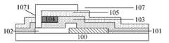
도 2는 본 개시내용의 예시적 실시예에 따른 TFT 어레이 기판의 일부의 구조체를 도시한다. 도 2에 도시된 바와 같이, TFT 어레이 기판은 베이스 기판(100), 베이스 기판(100) 상에 형성되는 제1 활성 층(102), 제1 활성 층(102)을 커버하는 제1 게이트 절연 층(103), 제1 게이트 절연 층(103) 상에 형성되는 게이트(104), 게이트(104)를 적어도 커버하는 제2 게이트 절연 층(105) 및 제2 게이트 절연 층(105) 상에 적어도 부분적으로 배치되는 제2 활성 층(107)을 포함한다. 제1 활성 층(102), 제1 게이트 절연 층(103) 및 게이트(104)는 제1 박막 트랜지스터의 일부를 형성하는 반면에, 게이트(104), 제2 게이트 절연 층(105) 및 제2 활성 층(107)은 제2 박막 트랜지스터의 일부를 형성한다. 더욱이, 제2 활성 층(107)은 제1 박막 트랜지스터가 제2 박막 트랜지스터에 직렬로 연결되도록 제1 활성 층(102)에 전기적으로 연결된다.2 illustrates a structure of a portion of a TFT array substrate in accordance with an exemplary embodiment of the present disclosure. As shown in FIG. 2, the TFT array substrate includes a
실시예에서, 서로 중첩되는 제1 박막 트랜지스터 및 제2 박막 트랜지스터는 게이트(104)를 공유하며, 그들 각각은 L의 채널 길이를 갖고, 그들의 전체 유효 채널 길이는 종래의 박막 트랜지스터의 채널 길이와 동일한 2L이다. 그러나, 한편으로, 기판 상에 점유되는 면적은 감소되는 것에 의해, 어레이 기판 및 고해상도를 갖는 디스플레이 패널 둘 다를 용이하게 하고; 다른 한편으로, 직렬로 연결되는 이러한 2개의 박막 트랜지스터들은 효과적으로 오프 상태 누설 전류(off-state leakage current)를 감소시키고 박막 트랜지스터들의 안정성을 증가시킬 수 있다.In an embodiment, the first thin film transistor and the second thin film transistor overlapping each other share a
일 예에서, 이러한 2개의 활성 층들(102, 107) 중 하나의 활성 층의 드레인 영역은 2개의 박막 트랜지스터들의 직렬 연결을 달성하기 위해, 이러한 2개의 활성 층들 중 다른 활성 층의 소스 영역에 전기적으로 연결된다. 예를 들어, 도 2에서, 소스 전극 층(101)이 베이스 기판(100) 상에 형성되고, 소스 전극 층(101)에 대한 제1 활성 층(102)의 소스 영역의 전기적 연결을 실현하기 위해, 제1 활성 층(102)의 소스 영역은 소스 전극 층(101)을 부분적으로 커버하거나 소스 전극 층(101)과 접촉한다. 더욱이, 제1 활성 층(102)의 드레인 영역은 제2 활성 층(107)의 소스 영역에 전기적으로 연결되고, 제2 활성 층(107)의 드레인 영역은 픽셀 전극 층(109)에 전기적으로 연결될 수 있다. 도 2에 도시된 바와 같이, 픽셀 전극 층(109)은 제2 활성 층(107) 및 제2 게이트 절연 층(105)을 커버하는 평탄화 층(108) 상에 배치될 수 있다.In one example, the drain region of one of these two
일 예에서, TFT 어레이 기판에는 제1 활성 층(102)의 드레인 영역을 노출하기 위해 제1 게이트 절연 층(103) 및 제2 게이트 절연 층(105)을 통해 연장되는 스루 홀(106)이 제공되고(도 4c 참조), 제2 활성 층(107)은 제1 활성 층(102)의 드레인 영역을 제2 활성 층(107)의 소스 영역에 전기적으로 연결하기 위해 스루 홀(106) 내에 위치되는 연결 부분(1071)을 포함할 수 있다. 일 예에서, 연결 부분(1071)은 제2 활성 층(107)과 동일한 재료로 형성될 수 있고, 대안적으로, 연결 부분(1071)은 그 안에서 캐리어 농도를 증가시키고, 온 상태(on state)에서 활성 층들 사이의 온 저항(on-resistance)을 감소시키기 위해 도핑된다.In one example, the TFT array substrate is provided with a through
도 3은 본 개시내용의 다른 예시적 실시예에 따른 TFT 어레이 기판의 일부의 구조체를 도시한다. 도 3에 도시된 바와 같이, TFT 어레이 기판은 베이스 기판(200), 베이스 기판(200) 상에 형성되는 제1 게이트(201), 제1 게이트(201)를 커버하는 제1 게이트 절연 층(202), 제1 게이트 절연 층(202) 상에 배치되는 제1 활성 층(204), 제1 활성 층(204)을 커버하는 층간 절연 층(205), 층간 절연 층(205) 상에 형성되는 제2 활성 층(206), 제2 활성 층(206)을 커버하는 제2 게이트 절연 층(207) 및 제2 게이트 절연 층(207) 상에 배치되는 제2 게이트(209)를 포함한다. 제1 게이트(201), 제1 게이트 절연 층(202) 및 제1 활성 층(204)은 제1 박막 트랜지스터의 일부를 형성하는 반면에, 제2 활성 층(206), 제2 게이트 절연 층(207) 및 제2 게이트(209)는 제2 박막 트랜지스터의 일부를 형성한다. 더욱이, 제2 활성 층(206)은 제1 박막 트랜지스터가 제2 박막 트랜지스터에 직렬로 연결되도록 제1 활성 층(204)에 전기적으로 연결된다.3 illustrates a structure of a portion of a TFT array substrate according to another exemplary embodiment of the present disclosure. As shown in FIG. 3, the TFT array substrate includes a
실시예에서, 서로 중첩되는 제1 박막 트랜지스터 및 제2 박막 트랜지스터는 L의 채널 길이를 각각 갖고, 그들의 전체 유효 채널 길이는 종래의 박막 트랜지스터의 채널 길이와 동일한 2L이다. 그러나, 한편으로, 기판 상에 점유되는 면적이 감소되는 것에 의해, 어레이 기판 및 고해상도가 되는 디스플레이 패널을 용이하게 하고; 다른 한편으로, 직렬로 연결되는 이러한 2개의 박막 트랜지스터들은 오프 상태 누설 전류를 효과적으로 감소시키고 박막 트랜지스터들의 안정성을 증가시킬 수 있다.In an embodiment, the first thin film transistor and the second thin film transistor overlapping each other have a channel length of L, respectively, and their total effective channel length is 2L, which is the same as the channel length of the conventional thin film transistor. On the one hand, however, the area occupied on the substrate is reduced, thereby facilitating the array substrate and the display panel to be high resolution; On the other hand, these two thin film transistors connected in series can effectively reduce the off-state leakage current and increase the stability of the thin film transistors.
일 예에서, 이러한 2개의 활성 층들(204, 206) 중 하나의 드레인 영역은 2개의 박막 트랜지스터들의 직렬 연결을 달성하기 위해, 이러한 2개의 활성 층들 중 다른 활성 층의 소스 영역에 전기적으로 연결된다. 예를 들어, 도 3에서, 소스 전극 층(203)이 제1 게이트 절연 층(202) 상에 형성되고, 소스 전극 층(203)에 대한 제1 활성 층(204)의 소스 영역의 전기적 연결을 실현하기 위해, 제1 활성 층(204)의 소스 영역은 소스 전극 층(203)과 부분적으로 중첩되거나 소스 전극 층(203)과 접촉한다. 더욱이, 제1 활성 층(204)의 드레인 영역은 제2 활성 층(206)의 소스 영역에 전기적으로 연결되고, 제2 활성 층(206)의 드레인 영역은 픽셀 전극 층(210)에 전기적으로 연결될 수 있다. 도 3에 도시된 바와 같이, 픽셀 전극 층(210)은 제2 게이트(209) 및 제2 게이트 절연 층(207)을 커버하는 평탄화 층(208) 상에 배치될 수 있다.In one example, the drain region of one of these two
일 예에서, TFT 어레이 기판에는 제1 활성 층(204)의 드레인 영역을 노출하기 위해 층간 절연 층(205)을 통해 연장되는 스루 홀이 제공되고, 제2 활성 층(206)은 제1 활성 층(204)의 드레인 영역을 제2 활성 층(206)의 소스 영역에 전기적으로 연결하기 위해 스루 홀(106) 내에 위치되는 연결 부분, 예를 들어, 도면에 도시된 바와 같이 제2 활성 층(206)의 소스 영역에서 제1 활성 층(204)의 드레인 영역까지 연장되는 수직 부분을 포함할 수 있다. 일 예에서, 연결 부분은 제2 활성 층(206)과 동일한 재료로 형성될 수 있고, 대안적으로, 연결 부분은 그 안에서 캐리어 농도를 증가시키고, 온 상태에서 활성 층들 사이의 온 저항을 감소시키기 위해 도핑된다.In one example, the TFT array substrate is provided with a through hole extending through the interlayer insulating
다른 양태에 따르면, 본 개시내용의 일 실시예는 또한 TFT 어레이 기판을 제조하는 방법을 제공하며, 방법은 베이스 기판을 제공하는 단계; 및 베이스 기판 상에 2개의 박막 트랜지스터들을 형성하는 단계를 포함하고, 박막 트랜지스터들은 소스 영역 및 드레인 영역을 갖는 활성 층을 각각 포함하고, 2개의 박막 트랜지스터들의 2개의 활성 층들은 베이스 기판에 수직인 방향으로 서로 중첩되고, 2개의 활성 층들 중 하나의 활성 층의 드레인 영역은 2개의 박막 트랜지스터들이 직렬로 연결될 때 2개의 활성 층들 중 다른 활성 층의 소스 영역에 전기적으로 연결된다.According to another aspect, an embodiment of the present disclosure also provides a method of manufacturing a TFT array substrate, the method comprising providing a base substrate; And forming two thin film transistors on the base substrate, wherein the thin film transistors each include an active layer having a source region and a drain region, wherein the two active layers of the two thin film transistors are perpendicular to the base substrate. Overlapping each other, the drain region of one of the two active layers is electrically connected to the source region of the other active layer of the two active layers when the two thin film transistors are connected in series.
다음에, 본 개시내용의 예시적 실시예에 따른 TFT 어레이 기판을 제조하는 방법은 도 4a 내지 도 4d를 참조하여 예로서 상세히 설명될 것이다.Next, a method of manufacturing a TFT array substrate according to an exemplary embodiment of the present disclosure will be described in detail by way of example with reference to FIGS. 4A-4D.
첫째로, 베이스 기판(100)이 제공된다. 베이스 기판은 사전에 세정되는 투명 기판, 예컨대, 유리 기판 등일 수 있고, 산화 실리콘, 질화 실리콘, 또는 둘 다의 적층된 조합으로 형성되는 버퍼 층은 활성 층으로 투명 기판 내의 금속 이온 불순물들의 확산으로 인해 박막 트랜지스터의 동작 특성들에 악영향을 미치는 것을 방지하기 위해, 베이스 기판에 도포될 수 있다.First, a
도 4a에 도시된 바와 같이, 제1 반도체 재료 층은 베이스 기판(100) 상에 형성되고, 제1 반도체 재료 층은 제1 활성 층(102)을 형성하기 위해 제1 마스크를 사용하여 패터닝된다.As shown in FIG. 4A, a first semiconductor material layer is formed on the
도 4b에 도시된 바와 같이, 제1 활성 층(102)을 커버하는 제1 게이트 절연 층(103)이 형성되고, 게이트 재료 층은 제1 게이트 절연 층(103) 상에 형성되고 게이트 재료 층은 제1 활성 층(102)보다 위에 위치되는 게이트(104)를 형성하기 위해 제2 마스크를 사용하여 패터닝된다. 게이트는 단일 층, 2개 이상의 층들의 구조체를 가질 수 있고, 금속 또는 금속 합금, 예컨대 몰리브덴, 알루미늄, 몰리브덴 텅스텐 등으로 제조될 수 있고, 그것의 두께는 1000Å 내지 5000Å의 범위, 대안적으로 1500Å 내지 4000Å의 범위일 수 있다.As shown in FIG. 4B, a first
도 4c에 도시된 바와 같이, 게이트(104) 및 제1 게이트 절연 층(103)을 커버하는 제2 게이트 절연 층(105)이 형성된다. 일 예에서, 제1 및/또는 제2 게이트 절연 층은 산화 실리콘, 질화 실리콘, 또는 둘 다의 적층된 조합의 단일 층일 수 있고, 본 개시내용은 이에 제한되지 않는다. 제1 및/또는 제2 게이트 절연 층은 PECVD, LPCVD, APCVD 또는 ECR-CVD 등에 의해 퇴적될 수 있고, 500Å 내지 2000Å의 퇴적 두께를 갖는다. 게다가, 적절한 두께, 예를 들어 600Å 내지 1500Å은 특정 설계 요건들에 따라 선택될 수 있다.As shown in FIG. 4C, a second
다음에, 제2 게이트 절연 층(105) 및 제1 게이트 절연 층(103)을 통해 연장되는 스루 홀(106)은 제1 활성 층(102)의 드레인 영역을 노출하기 위해 제3 마스크를 사용함으로써 형성된다.Next, the through
그 다음에, 도 4d에 도시된 바와 같이, 제2 반도체 재료 층이 제2 게이트 절연 층(105) 상에 형성되고 제2 반도체 재료 층은 제2 활성 층(107)을 형성하기 위해 상기 설명된 바와 같이 제1 마스크를 사용하여 패터닝된다. 제2 활성 층의 일부가 제1 활성 층(102)의 드레인 영역을 제2 활성 층(107)의 소스 영역에 전기적으로 연결하는 연결 부분(1071)을 형성하기 위해 스루 홀 내에 위치된다. 일 예에서, 제1 및/또는 제2 활성 층은 폴리실리콘 층일 수 있으며, 폴리실리콘 층은 엑시머 레이저 결정화, 금속 유도 결정화 또는 고체상 결정화 등의 공정에 의해 비정질 실리콘 층으로 변환되는 것에 의해, 저온 폴리실리콘 어레이 기판을 형성한다. 상이한 결정화 방법들에 따라, 박막 트랜지스터들의 특정 공정들 및 구조체들이 상이한 점이 주목되어야 한다. 예를 들어, 준비 공정에서, 본 개시내용의 구현에 영향을 미치는 것 없이, 열 처리 탈수소화, 유도 금속의 퇴적, 열 처리 결정화, 엑시머 레이저 조명 결정화, 소스 및 드레인 영역들의 도핑(P형 또는 N형 도핑), 도핑된 불순물의 활성화를 포함하는 것이 가능하다. 그러한 상황에서, 본 개시내용은 또한 유익한 효과를 가질 것이다. 예시적으로, 제1 및/또는 제2 활성 층의 두께는 100Å 내지 3000Å, 구체적으로 500Å 내지 1000Å일 수 있고, 그것의 형성 방법은 PECVD, LPCVD 또는 스퍼터링 방법일 수 있고, 퇴적 온도는 600℃보다 아래이다.Next, as shown in FIG. 4D, a second semiconductor material layer is formed on the second
일 실시예에서, 도 4a에 여전히 도시된 바와 같이, 제1 활성 층(102)을 형성하는 단계 전에, 또는 제1 활성 층(102)을 형성하는 단계 후이지만 제1 게이트 절연 층(103)을 형성하기 전에, 방법은 베이스 기판 상에 전기 전도성 재료 층을 형성하고 제4 마스크를 사용함으로써 전기 전도성 재료 층을 패터닝하여 소스 전극 층(101)을 획득하는 단계를 더 포함하며, 제1 활성 층(102)의 일부는 소스 전극 층(101)의 일부와 중첩된다.In one embodiment, as shown in FIG. 4A, the first
게다가, 게이트(104)를 형성한 후이지만 제2 게이트 절연 층(105)을 형성하기 전에, 제1 이온 주입 공정은 제1 활성 층(102)의 소스 영역 및 드레인 영역에 이온 도핑 공정을 구현하기 위해, 차폐 마스크로서 게이트(104)를 사용함으로써 구현될 수 있고; 제2 활성 층(107)을 형성한 후에, 제2 이온 주입 공정은 제2 활성 층(107)의 소스 영역 및 드레인 영역에 이온 도핑 공정을 구현하기 위해, 다른 차폐 마스크로서 상기 설명된 제2 마스크를 사용함으로써 구현될 수 있다. 대안적으로, 제2 활성 층(107)을 형성한 후에, 이온 주입 공정은 제1 활성 층(102) 및 제2 활성 층(107)의 소스 영역들 및 드레인 영역들에 이온 도핑 공정을 구현하기 위해, 차폐 마스크로서 상기 설명된 제2 마스크를 사용함으로써 구현될 수 있다. 스루 홀 내에 위치되는 제2 활성 층의 연결 부분은 또한 그 안에서 캐리어 농도를 증가시키고, 온 상태에서 활성 층들 사이의 온 저항을 감소시키기 위해, 이온 도핑 공정이 제2 활성 층에 구현될 때 도핑될 수 있다는 점이 이해될 것이다.In addition, after forming the
이온 주입 공정은 질량 분석계를 갖는 이온 주입 방법, 질량 분석계를 갖지 않는 이온 클라우드 타입 주입 방법(ion cloud-type implantation method), 플라즈마 주입 방법, 고체 상태 확산 주입 방법 등일 수 있다. 예를 들어, 대중적인 이온 클라우드 타입 주입 방법이 사용되면, 이때 붕소 예컨대 B2H6/H2 또는 인 예컨대 PH3/H2를 포함하는 혼합 가스는 설계 요건들에 따라 주입될 수 있고, 이온 주입 에너지는 10 내지 200keV, 구체적으로 40 내지 100keV일 수 있다. 주입 선량은 1×10¹¹~1×10²⁰ 원자들/㎤, 구체적으로 1×10¹⁴~1×10¹⁸ 원자들/㎤의 범위일 수 있다.The ion implantation process may be an ion implantation method with a mass spectrometer, an ion cloud-type implantation method without a mass spectrometer, a plasma implantation method, a solid state diffusion implantation method, or the like. For example, if the popular ion cloud type implantation method is used, then a mixed gas comprising boron such as B2 H6 / H2 or phosphorus such as PH3 / H2 may be injected according to design requirements, and The implantation energy may be 10 to 200 keV, specifically 40 to 100 keV. The injection dose may range from 1 × 10¹¹ to 1 × 10²⁰ atoms /
도 2에 도시된 바와 같이, 제2 활성 층(107) 및 제2 게이트 절연 층(105)을 커버하는 평탄화 층(108)은 제5 마스크를 사용함으로써 형성될 수 있고; 픽셀 전극 층(109)은 제6 마스크를 사용함으로써 평탄화 층(108) 상에 형성될 수 있으며, 픽셀 전극 층(109)은 제2 활성 층(107)의 드레인 영역에 전기적으로 연결된다. 평탄화 층은 유기 재료, 구체적으로 유기 포토레지스트 재료 예컨대 폴리이미드, 아크릴 등으로 제조될 수 있으며, 8000Å 내지 20000Å의 두께를 갖는다. 픽셀 전극 층은 단일 층, 2개 또는 그 이상의 층들의 구조체일 수 있고, 투명 전도성 재료, 예컨대, 인듐 주석 산화물, 인듐 아연 산화물 또는 이와 유사한 것, 또는 금속, 금속 합금, 예를 들어, 은, 은 합금 또는 이와 유사한 것으로 구성되고, 1000Å 내지 5000Å, 구체적으로는 1500Å 내지 4000Å의 두께를 갖는다.As shown in FIG. 2, the planarization layer 108 covering the second
본 개시내용의 실시예들에 따른 방법은 또한 종래의 공정들과 비교하여 마스크들의 수를 증가시키는 것 없이, TFT 어레이 기판을 제조하기 위해 6개의 마스크들을 사용하는 것이 인식될 수 있다. 따라서, 방법은 부가 공정들을 포함하지 않고 공정 실현에서 공정 복잡성을 증가시키지 않으며, 제조된 디바이스는 더 좋은 성질을 갖는다.It can be appreciated that the method according to embodiments of the present disclosure also uses six masks to manufacture a TFT array substrate, without increasing the number of masks as compared to conventional processes. Thus, the method does not include additional processes and does not increase process complexity in process realization, and the manufactured device has better properties.
게다가, 본 개시내용의 일 실시예에서, 상기 설명된 실시예들 중 어느 하나에 따른 TFT 어레이 기판, 또는 상기 설명된 실시예들 중 어느 하나에 따른 방법에 의해 제조되는 TFT 어레이 기판을 포함하는 디스플레이 디바이스가 제공된다. 그러한 디스플레이 디바이스는 디스플레이 기능을 갖는 액정 패널, 전자 종이, OLED 패널, 이동 전화, 노트북 컴퓨터, 태블릿 컴퓨터, 디스플레이, 디지털 포토 프레임, 내비게이터, 식별 디바이스, 또는 임의의 다른 제품들 또는 구성요소들일 수 있다.In addition, in one embodiment of the present disclosure, a display comprising a TFT array substrate according to any one of the embodiments described above, or a TFT array substrate manufactured by a method according to any of the embodiments described above. A device is provided. Such display device may be a liquid crystal panel, electronic paper, OLED panel, mobile phone, notebook computer, tablet computer, display, digital photo frame, navigator, identification device, or any other products or components having a display function.
본 개시내용의 다양한 예시적 실시예들이 도시되고 설명되었지만, 변경들 및 수정들은 본 개시내용의 원리 및 사상으로부터 벗어나는 것 없이 이러한 실시예들에 이루어질 수 있고, 본 개시내용의 범위는 첨부된 청구항들 및 그들의 균등물들에 의해 정의된다는 점이 본 기술분야의 통상의 기술자들에 의해 이해될 것이다.While various example embodiments of the disclosure have been shown and described, changes and modifications can be made to such embodiments without departing from the spirit and spirit of the disclosure, the scope of the disclosure being appended to the claims And their equivalents will be understood by those of ordinary skill in the art.
Claims (19)
Translated fromKorean베이스 기판; 및
상기 베이스 기판 상에 위치되는 2개의 박막 트랜지스터들
을 포함하고, 상기 2개의 박막 트랜지스터들은 소스 영역 및 드레인 영역을 갖는 활성 층을 각각 포함하고, 상기 2개의 박막 트랜지스터들의 2개의 활성 층들은 상기 베이스 기판에 수직인 방향으로 서로 중첩되고, 상기 2개의 활성 층들 중 하나의 활성 층의 상기 드레인 영역은 상기 2개의 박막 트랜지스터들이 직렬로 연결되도록 스루 홀(through hole)을 통해 상기 2개의 활성 층들 중 다른 활성 층의 상기 소스 영역에 전기적으로 연결되고,
상기 2개의 활성 층들은 상기 베이스 기판 상에 형성된 제1 활성 층 및 상기 베이스 기판에 대하여 원위의(distal) 상기 제1 활성 층의 일 측에 배치된 제2 활성 층을 포함하고, 상기 제2 활성 층은 상기 제1 활성 층의 상기 드레인 영역을 상기 제2 활성 층의 상기 소스 영역에 직접적으로 연결하는 연결 부분을 포함하고, 상기 제2 활성 층의 일부는 상기 연결 부분을 형성하는, TFT 어레이 기판.As a TFT array substrate,
A base substrate; And
Two thin film transistors positioned on the base substrate
Wherein the two thin film transistors each include an active layer having a source region and a drain region, wherein the two active layers of the two thin film transistors overlap each other in a direction perpendicular to the base substrate, The drain region of one of the active layers is electrically connected to the source region of the other active layer of the two active layers through a through hole such that the two thin film transistors are connected in series,
The two active layers comprise a first active layer formed on the base substrate and a second active layer disposed on one side of the first active layer distal to the base substrate, the second active layer A layer comprising a connecting portion directly connecting said drain region of said first active layer to said source region of said second active layer, wherein a portion of said second active layer forms said connecting portion .
상기 2개의 박막 트랜지스터들 중 다른 박막 트랜지스터는 상기 제1 활성 층 위에 위치되는 상기 제2 활성 층, 상기 제2 활성 층을 커버하는 제2 게이트 절연 층 및 상기 제2 게이트 절연 층 상에 위치되는 제2 게이트를 포함하고,
상기 제2 활성 층의 상기 소스 영역은 상기 제1 활성 층의 상기 드레인 영역에 전기적으로 연결되는 TFT 어레이 기판.The semiconductor device of claim 1, wherein one of the two thin film transistors comprises: a first gate positioned on the base substrate, a first gate insulating layer covering the first gate, and a first gate insulating layer; The first active layer located at,
Another thin film transistor of the two thin film transistors may include a second active layer positioned above the first active layer, a second gate insulating layer covering the second active layer, and a second gate insulating layer positioned on the second gate insulating layer. Includes 2 gates,
And the source region of the second active layer is electrically connected to the drain region of the first active layer.
상기 제1 활성 층과 상기 베이스 기판 사이에 있고 상기 제1 활성 층의 상기 소스 영역에 전기적으로 연결되는 소스 전극 층, 및
상기 베이스 기판에 대하여 원위의 상기 제2 활성 층의 일 측 상에 있고, 상기 제2 활성 층의 상기 드레인 영역에 전기적으로 연결되는 픽셀 전극 층
을 더 포함하는 TFT 어레이 기판.The method according to any one of claims 2 to 6,
A source electrode layer between the first active layer and the base substrate and electrically connected to the source region of the first active layer, and
A pixel electrode layer on one side of the second active layer distal to the base substrate and electrically connected to the drain region of the second active layer
TFT array substrate further comprising.
베이스 기판을 제공하는 단계; 및
상기 베이스 기판 상에 2개의 박막 트랜지스터들을 형성하는 단계
를 포함하고, 상기 2개의 박막 트랜지스터들은 소스 영역 및 드레인 영역을 갖는 활성 층을 각각 포함하고, 상기 2개의 박막 트랜지스터들의 2개의 활성 층들은 상기 베이스 기판에 수직인 방향으로 서로 중첩되고, 상기 2개의 활성 층들 중 하나의 활성 층의 상기 드레인 영역은 상기 2개의 박막 트랜지스터들이 직렬로 연결되도록 스루 홀을 통해 상기 2개의 활성 층들 중 다른 활성 층의 상기 소스 영역에 전기적으로 연결되고,
상기 2개의 박막 트랜지스터들을 형성하는 단계는,
상기 베이스 기판 상에 제1 반도체 재료 층을 형성하고 제1 마스크로 상기 제1 반도체 재료 층을 패터닝하여 제1 활성 층을 형성하는 단계;
상기 제1 활성 층을 커버하는 제1 게이트 절연 층을 형성하는 단계;
상기 제1 게이트 절연 층 상에 게이트 재료 층을 형성하고 제2 마스크로 상기 게이트 재료 층을 패터닝하여 상기 제1 활성 층 위에 위치되는 게이트를 형성하는 단계;
상기 게이트 및 상기 제1 게이트 절연 층을 커버하는 제2 게이트 절연 층을 형성하는 단계;
상기 제1 활성 층의 상기 드레인 영역을 노출하기 위해 제3 마스크를 사용함으로써 상기 제2 게이트 절연 층 및 상기 제1 게이트 절연 층을 통해 연장되는 상기 스루 홀을 형성하는 단계; 및
상기 제2 게이트 절연 층 상에 제2 반도체 재료 층을 형성하고 상기 제1 마스크로 상기 제2 반도체 재료 층을 패터닝하여 제2 활성 층을 형성하는 단계를 포함하고, 상기 제2 활성 층의 일부가 상기 제1 활성 층의 상기 드레인 영역을 상기 제2 활성 층의 상기 소스 영역에 전기적으로 연결하는 연결 부분을 형성하기 위해 상기 스루 홀 내에 위치되는, 방법.As a method of manufacturing a TFT array substrate,
Providing a base substrate; And
Forming two thin film transistors on the base substrate
Wherein the two thin film transistors each include an active layer having a source region and a drain region, wherein the two active layers of the two thin film transistors overlap each other in a direction perpendicular to the base substrate, The drain region of one of the active layers is electrically connected to the source region of the other active layer of the two active layers through a through hole such that the two thin film transistors are connected in series,
Forming the two thin film transistors,
Forming a first semiconductor material layer on the base substrate and patterning the first semiconductor material layer with a first mask to form a first active layer;
Forming a first gate insulating layer covering the first active layer;
Forming a gate material layer on the first gate insulating layer and patterning the gate material layer with a second mask to form a gate positioned over the first active layer;
Forming a second gate insulating layer covering the gate and the first gate insulating layer;
Forming the through hole extending through the second gate insulating layer and the first gate insulating layer by using a third mask to expose the drain region of the first active layer; And
Forming a second semiconductor material layer on the second gate insulating layer and patterning the second semiconductor material layer with the first mask to form a second active layer, wherein a portion of the second active layer is Located in the through hole to form a connection portion electrically connecting the drain region of the first active layer to the source region of the second active layer.
비정질 실리콘 층을 형성하는 단계; 및
엑시머 레이저 결정화(excimer laser crystallization), 금속 유도 결정화(metal induced crystallization) 또는 고체상 결정화(solid phase crystallization)의 공정에 의해 상기 비정질 실리콘 층을 폴리실리콘 층으로 변환하는 단계를 포함하는 방법.The method of claim 10, wherein forming the first semiconductor material layer and / or forming the second semiconductor material layer,
Forming an amorphous silicon layer; And
Converting the amorphous silicon layer to a polysilicon layer by a process of excimer laser crystallization, metal induced crystallization, or solid phase crystallization.
상기 베이스 기판 상에 전기 전도성 재료 층을 형성하고 제4 마스크를 사용함으로써 상기 전기 전도성 재료 층을 패터닝하여 소스 전극 층을 획득하는 단계를 더 포함하며, 상기 제1 활성 층의 일부가 상기 소스 전극 층의 일부와 중첩되는 방법.The method of claim 10, wherein before the forming of the first active layer or after forming the first active layer but before forming the first gate insulating layer, the method further comprises:
Forming a layer of electrically conductive material on the base substrate and patterning the layer of electrically conductive material by using a fourth mask to obtain a source electrode layer, a portion of the first active layer being the source electrode layer How to overlap with part of.
상기 게이트를 형성한 후이지만, 상기 제2 게이트 절연 층을 형성하기 전에, 상기 제1 활성 층의 상기 소스 영역 및 상기 드레인 영역에 이온 도핑 공정을 구현하기 위해, 차폐 마스크(shielding mask)로서 상기 게이트를 사용함으로써 제1 이온 주입 공정을 구현하는 단계; 및
상기 제2 활성 층을 형성한 후에, 상기 제2 활성 층의 상기 소스 영역 및 상기 드레인 영역에 이온 도핑 공정을 구현하기 위해, 다른 차폐 마스크로서 상기 제2 마스크를 사용함으로써 제2 이온 주입 공정을 구현하는 단계를 더 포함하는 방법.The method of claim 10,
After forming the gate, but before forming the second gate insulating layer, the gate as a shielding mask to implement an ion doping process in the source region and the drain region of the first active layer. Implementing a first ion implantation process by using; And
After forming the second active layer, a second ion implantation process is implemented by using the second mask as another shielding mask to implement an ion doping process in the source region and the drain region of the second active layer. The method further comprises the step.
상기 제2 활성 층을 형성한 후에, 상기 제1 활성 층 및 상기 제2 활성 층의 상기 소스 영역들 및 상기 드레인 영역들에 이온 도핑 공정을 구현하기 위해, 차폐 마스크로서 상기 제2 마스크를 사용함으로써 이온 주입 공정을 구현하는 단계를 더 포함하는 방법.The method of claim 10,
After forming the second active layer, by using the second mask as a shielding mask to implement an ion doping process in the source and drain regions of the first and second active layers. Implementing the ion implantation process.
제5 마스크를 사용함으로써 상기 제2 활성 층 및 상기 제2 게이트 절연 층을 커버하기 위해 상기 베이스 기판 위에 평탄화 층을 형성하는 단계; 및
제6 마스크를 사용함으로써 상기 평탄화 층 상에 픽셀 전극 층을 형성하는 단계를 더 포함하고, 상기 픽셀 전극 층은 상기 제2 활성 층의 상기 드레인 영역에 전기적으로 연결되는 방법.The method according to any one of claims 10 and 12 to 15,
Forming a planarization layer over the base substrate to cover the second active layer and the second gate insulating layer by using a fifth mask; And
Forming a pixel electrode layer on the planarization layer by using a sixth mask, wherein the pixel electrode layer is electrically connected to the drain region of the second active layer.
Applications Claiming Priority (3)
| Application Number | Priority Date | Filing Date | Title |
|---|---|---|---|
| CN201610202895.6ACN105633101A (en) | 2016-04-01 | 2016-04-01 | TFT array substrate and manufacture method thereof, and display device |
| CN201610202895.6 | 2016-04-01 | ||
| PCT/CN2016/084947WO2017166431A1 (en) | 2016-04-01 | 2016-06-06 | Tft array substrate and manufacturing method therefor, and display device |
Publications (2)
| Publication Number | Publication Date |
|---|---|
| KR20170124523A KR20170124523A (en) | 2017-11-10 |
| KR102055247B1true KR102055247B1 (en) | 2019-12-11 |
Family
ID=56047853
Family Applications (1)
| Application Number | Title | Priority Date | Filing Date |
|---|---|---|---|
| KR1020177015359AActiveKR102055247B1 (en) | 2016-04-01 | 2016-06-06 | Tft array substrate, method for manufacturing the same, and display device |
Country Status (6)
| Country | Link |
|---|---|
| US (1) | US10325938B2 (en) |
| EP (1) | EP3439035A4 (en) |
| JP (1) | JP6896627B2 (en) |
| KR (1) | KR102055247B1 (en) |
| CN (1) | CN105633101A (en) |
| WO (1) | WO2017166431A1 (en) |
Families Citing this family (21)
| Publication number | Priority date | Publication date | Assignee | Title |
|---|---|---|---|---|
| CN105633101A (en)* | 2016-04-01 | 2016-06-01 | 京东方科技集团股份有限公司 | TFT array substrate and manufacture method thereof, and display device |
| US11328951B2 (en) | 2016-04-01 | 2022-05-10 | Intel Corporation | Transistor cells including a deep via lined wit h a dielectric material |
| KR102548835B1 (en) | 2016-08-26 | 2023-06-30 | 인텔 코포레이션 | Integrated circuit device structures and double sided fabrication techniques |
| CN106206430B (en)* | 2016-10-11 | 2021-01-01 | 深圳市华星光电技术有限公司 | Manufacturing method of thin film transistor structure |
| CN107068694B (en)* | 2017-04-26 | 2019-10-01 | 厦门天马微电子有限公司 | Semiconductor device structure and preparation method thereof, array substrate and display device |
| DE112017008080T5 (en) | 2017-12-26 | 2020-07-09 | Intel Corporation | STACKED TRANSISTORS WITH LAST TRAINED CONTACT |
| US11430814B2 (en) | 2018-03-05 | 2022-08-30 | Intel Corporation | Metallization structures for stacked device connectivity and their methods of fabrication |
| KR102691133B1 (en) | 2018-09-13 | 2024-08-01 | 엘지디스플레이 주식회사 | TFT substrate and light emitting display device including the same |
| CN109786396B (en) | 2019-01-30 | 2021-04-09 | 华为技术有限公司 | Array substrate, display screen and terminal equipment |
| US11688780B2 (en) | 2019-03-22 | 2023-06-27 | Intel Corporation | Deep source and drain for transistor structures with back-side contact metallization |
| CN110299377B (en)* | 2019-07-03 | 2022-12-16 | 京东方科技集团股份有限公司 | Display substrate, manufacturing method, and display device |
| CN110581142A (en)* | 2019-08-23 | 2019-12-17 | 武汉华星光电技术有限公司 | Array substrate, manufacturing method thereof, and display panel |
| CN110690257A (en)* | 2019-08-29 | 2020-01-14 | 福建华佳彩有限公司 | TFT array substrate and manufacturing method thereof |
| CN110648629B (en)* | 2019-10-31 | 2023-09-22 | 厦门天马微电子有限公司 | Display panel, manufacturing method and display device thereof |
| CN111029342B (en) | 2019-11-07 | 2024-04-16 | 深圳市华星光电半导体显示技术有限公司 | Display panel, preparation method thereof and display device |
| CN110854203B (en)* | 2019-11-21 | 2023-10-03 | 京东方科技集团股份有限公司 | Thin film transistor, array substrate, display panel and display device |
| CN111063703B (en)* | 2019-12-10 | 2022-11-01 | Tcl华星光电技术有限公司 | Array substrate and display device |
| CN112490275B (en)* | 2020-12-03 | 2023-04-21 | 湖北长江新型显示产业创新中心有限公司 | Display panel, manufacturing method thereof and display device |
| CN114220819A (en)* | 2021-10-29 | 2022-03-22 | 长沙惠科光电有限公司 | Array substrate, preparation method thereof and display panel |
| CN115274554A (en)* | 2022-06-22 | 2022-11-01 | 京东方科技集团股份有限公司 | Manufacturing method of driving circuit, driving circuit and display module |
| CN115274861B (en)* | 2022-07-27 | 2025-08-08 | 武汉华星光电技术有限公司 | Semiconductor devices and electronic devices |
Citations (4)
| Publication number | Priority date | Publication date | Assignee | Title |
|---|---|---|---|---|
| JP2005294851A (en)* | 2004-04-05 | 2005-10-20 | Quanta Display Inc | Low temperature polysilicon TFT structure and method of manufacturing channel layer thereof |
| US20090014799A1 (en) | 2007-07-11 | 2009-01-15 | Semiconductor Energy Laboratory Co., Ltd. | Semiconductor device and method for manufacturing the same |
| CN104867942A (en) | 2015-04-29 | 2015-08-26 | 深圳市华星光电技术有限公司 | Fabrication method of thin film transistor (TFT) substrate and structure thereof |
| US20150311265A1 (en) | 2014-04-23 | 2015-10-29 | Nlt Technologies, Ltd. | Pixel array, electro-optic device, and electric apparatus |
Family Cites Families (21)
| Publication number | Priority date | Publication date | Assignee | Title |
|---|---|---|---|---|
| JP2969864B2 (en) | 1990-08-28 | 1999-11-02 | ソニー株式会社 | Semiconductor memory device |
| JP2830447B2 (en) | 1990-10-15 | 1998-12-02 | 日本電気株式会社 | Semiconductor nonvolatile storage device |
| DE69327028T2 (en)* | 1992-09-25 | 2000-05-31 | Sony Corp., Tokio/Tokyo | Liquid crystal display device |
| JPH06291269A (en)* | 1993-04-06 | 1994-10-18 | Sony Corp | Filed-effect transistor |
| JPH08148693A (en)* | 1994-09-22 | 1996-06-07 | Sanyo Electric Co Ltd | Thin-film transistor and manufacture thereof |
| JP2001066636A (en) | 1999-08-31 | 2001-03-16 | Hitachi Ltd | Liquid crystal display |
| KR100746220B1 (en) | 2004-01-12 | 2007-08-03 | 삼성전자주식회사 | Semiconductor integrated circuits employing stacked node contact structures and stacked thin film transistors and methods of fabricating the same |
| US7579220B2 (en)* | 2005-05-20 | 2009-08-25 | Semiconductor Energy Laboratory Co., Ltd. | Semiconductor device manufacturing method |
| JP5088661B2 (en) | 2006-12-05 | 2012-12-05 | セイコーエプソン株式会社 | Semiconductor device and electro-optical device |
| DE102007030054B4 (en)* | 2007-06-29 | 2009-04-16 | Advanced Micro Devices, Inc., Sunnyvale | Transistor with reduced gate resistance and improved stress transfer efficiency and method of making the same |
| US9279751B2 (en)* | 2008-12-16 | 2016-03-08 | Nico Corporation | System and method of taking and collecting tissue cores for treatment |
| JP5470519B2 (en)* | 2009-07-24 | 2014-04-16 | 株式会社ブイ・テクノロジー | Thin film transistor, manufacturing method thereof, and liquid crystal display device |
| US8981367B2 (en)* | 2011-12-01 | 2015-03-17 | Semiconductor Energy Laboratory Co., Ltd. | Semiconductor device |
| TW201338102A (en)* | 2012-03-14 | 2013-09-16 | Wintek Corp | Active component and active device array substrate |
| CN103367353A (en)* | 2012-03-30 | 2013-10-23 | 东莞万士达液晶显示器有限公司 | Active components and active component array substrates |
| JP6410496B2 (en)* | 2013-07-31 | 2018-10-24 | 株式会社半導体エネルギー研究所 | Multi-gate transistor |
| CN103730485B (en)* | 2013-12-27 | 2016-09-07 | 京东方科技集团股份有限公司 | OLED array of double-sided display and preparation method thereof, display device |
| KR102401432B1 (en)* | 2014-02-24 | 2022-05-26 | 엘지디스플레이 주식회사 | Display device |
| TW201611298A (en)* | 2014-09-12 | 2016-03-16 | 中華映管股份有限公司 | Double film transistor and manufacturing method thereof |
| CN104882414B (en) | 2015-05-06 | 2018-07-10 | 深圳市华星光电技术有限公司 | The production method and its structure of TFT substrate |
| CN105633101A (en)* | 2016-04-01 | 2016-06-01 | 京东方科技集团股份有限公司 | TFT array substrate and manufacture method thereof, and display device |
- 2016
- 2016-04-01CNCN201610202895.6Apatent/CN105633101A/enactivePending
- 2016-06-06EPEP16865283.2Apatent/EP3439035A4/enactivePending
- 2016-06-06JPJP2017531238Apatent/JP6896627B2/enactiveActive
- 2016-06-06WOPCT/CN2016/084947patent/WO2017166431A1/ennot_activeCeased
- 2016-06-06KRKR1020177015359Apatent/KR102055247B1/enactiveActive
- 2016-06-06USUS15/531,154patent/US10325938B2/enactiveActive
Patent Citations (6)
| Publication number | Priority date | Publication date | Assignee | Title |
|---|---|---|---|---|
| JP2005294851A (en)* | 2004-04-05 | 2005-10-20 | Quanta Display Inc | Low temperature polysilicon TFT structure and method of manufacturing channel layer thereof |
| US20060008953A1 (en) | 2004-04-05 | 2006-01-12 | Cheng Chang Kuo | Structure of ltps-tft and method of fabricating channel layer thereof |
| US20090014799A1 (en) | 2007-07-11 | 2009-01-15 | Semiconductor Energy Laboratory Co., Ltd. | Semiconductor device and method for manufacturing the same |
| JP2009038368A (en)* | 2007-07-11 | 2009-02-19 | Semiconductor Energy Lab Co Ltd | Semiconductor device, electronic device, and method for manufacturing semiconductor device |
| US20150311265A1 (en) | 2014-04-23 | 2015-10-29 | Nlt Technologies, Ltd. | Pixel array, electro-optic device, and electric apparatus |
| CN104867942A (en) | 2015-04-29 | 2015-08-26 | 深圳市华星光电技术有限公司 | Fabrication method of thin film transistor (TFT) substrate and structure thereof |
Also Published As
| Publication number | Publication date |
|---|---|
| EP3439035A4 (en) | 2019-11-06 |
| CN105633101A (en) | 2016-06-01 |
| KR20170124523A (en) | 2017-11-10 |
| JP2019511831A (en) | 2019-04-25 |
| US20180197895A1 (en) | 2018-07-12 |
| US10325938B2 (en) | 2019-06-18 |
| EP3439035A1 (en) | 2019-02-06 |
| JP6896627B2 (en) | 2021-06-30 |
| WO2017166431A1 (en) | 2017-10-05 |
Similar Documents
| Publication | Publication Date | Title |
|---|---|---|
| KR102055247B1 (en) | Tft array substrate, method for manufacturing the same, and display device | |
| CN109273404B (en) | Array substrate, preparation method thereof, display panel and display device | |
| CN107424957B (en) | Manufacturing method of flexible TFT substrate | |
| JP2019511831A5 (en) | ||
| CN110649101B (en) | Thin film transistor, manufacturing method thereof, array substrate and display device | |
| US11121226B2 (en) | Thin film transistor and method for manufacturing the same, array substrate and display device | |
| US20150129865A1 (en) | Semiconductor device and method for manufacturing same | |
| CN105762196B (en) | A kind of thin film transistor (TFT), its production method and related device | |
| KR20080012768A (en) | Display device and manufacturing method thereof | |
| US12156432B2 (en) | Display panel and display device | |
| KR20210086247A (en) | Display apparatus | |
| TW200302386A (en) | Semiconductor display device, method for making the same, and active matrix type display device | |
| JP4993826B2 (en) | Method for manufacturing semiconductor device | |
| JP6291015B2 (en) | Semiconductor device | |
| CN108257975B (en) | Array substrate and preparation method thereof, display device and preparation method of thin film transistor | |
| CN101399273B (en) | Image display system and manufacturing method thereof | |
| JP4986347B2 (en) | Method for manufacturing semiconductor device | |
| CN113451207B (en) | Array substrate, preparation method and display device | |
| KR102145978B1 (en) | Array substrate and method for fabricating of the same | |
| US8754418B2 (en) | Semiconductor device, and method for producing same | |
| CN106711155A (en) | Array substrate, display panel and display device | |
| CN119230556A (en) | Display substrate and display panel | |
| JP2001057434A (en) | Semiconductor device |
Legal Events
| Date | Code | Title | Description |
|---|---|---|---|
| PA0105 | International application | Patent event date:20170605 Patent event code:PA01051R01D Comment text:International Patent Application | |
| A201 | Request for examination | ||
| PA0201 | Request for examination | Patent event code:PA02012R01D Patent event date:20170629 Comment text:Request for Examination of Application | |
| PG1501 | Laying open of application | ||
| E902 | Notification of reason for refusal | ||
| PE0902 | Notice of grounds for rejection | Comment text:Notification of reason for refusal Patent event date:20180918 Patent event code:PE09021S01D | |
| E902 | Notification of reason for refusal | ||
| PE0902 | Notice of grounds for rejection | Comment text:Notification of reason for refusal Patent event date:20190329 Patent event code:PE09021S01D | |
| E701 | Decision to grant or registration of patent right | ||
| PE0701 | Decision of registration | Patent event code:PE07011S01D Comment text:Decision to Grant Registration Patent event date:20190923 | |
| GRNT | Written decision to grant | ||
| PR0701 | Registration of establishment | Comment text:Registration of Establishment Patent event date:20191204 Patent event code:PR07011E01D | |
| PR1002 | Payment of registration fee | Payment date:20191205 End annual number:3 Start annual number:1 | |
| PG1601 | Publication of registration | ||
| PR1001 | Payment of annual fee | Payment date:20221129 Start annual number:4 End annual number:4 | |
| PR1001 | Payment of annual fee | Payment date:20231017 Start annual number:5 End annual number:5 | |
| PR1001 | Payment of annual fee | Payment date:20241016 Start annual number:6 End annual number:6 |