KR102053258B1 - Touch window - Google Patents
Touch windowDownload PDFInfo
- Publication number
- KR102053258B1 KR102053258B1KR1020140003985AKR20140003985AKR102053258B1KR 102053258 B1KR102053258 B1KR 102053258B1KR 1020140003985 AKR1020140003985 AKR 1020140003985AKR 20140003985 AKR20140003985 AKR 20140003985AKR 102053258 B1KR102053258 B1KR 102053258B1
- Authority
- KR
- South Korea
- Prior art keywords
- electrode
- sensing electrode
- reinforcing
- sensing
- wiring
- Prior art date
- Legal status (The legal status is an assumption and is not a legal conclusion. Google has not performed a legal analysis and makes no representation as to the accuracy of the status listed.)
- Active
Links
Images


Classifications
- G—PHYSICS
- G06—COMPUTING OR CALCULATING; COUNTING
- G06F—ELECTRIC DIGITAL DATA PROCESSING
- G06F3/00—Input arrangements for transferring data to be processed into a form capable of being handled by the computer; Output arrangements for transferring data from processing unit to output unit, e.g. interface arrangements
- G06F3/01—Input arrangements or combined input and output arrangements for interaction between user and computer
- G06F3/03—Arrangements for converting the position or the displacement of a member into a coded form
- G06F3/041—Digitisers, e.g. for touch screens or touch pads, characterised by the transducing means
- G06F3/044—Digitisers, e.g. for touch screens or touch pads, characterised by the transducing means by capacitive means
- G06F3/0443—Digitisers, e.g. for touch screens or touch pads, characterised by the transducing means by capacitive means using a single layer of sensing electrodes
- G—PHYSICS
- G06—COMPUTING OR CALCULATING; COUNTING
- G06F—ELECTRIC DIGITAL DATA PROCESSING
- G06F3/00—Input arrangements for transferring data to be processed into a form capable of being handled by the computer; Output arrangements for transferring data from processing unit to output unit, e.g. interface arrangements
- G06F3/01—Input arrangements or combined input and output arrangements for interaction between user and computer
- G06F3/03—Arrangements for converting the position or the displacement of a member into a coded form
- G06F3/041—Digitisers, e.g. for touch screens or touch pads, characterised by the transducing means
- G06F3/0412—Digitisers structurally integrated in a display
- G—PHYSICS
- G06—COMPUTING OR CALCULATING; COUNTING
- G06F—ELECTRIC DIGITAL DATA PROCESSING
- G06F2203/00—Indexing scheme relating to G06F3/00 - G06F3/048
- G06F2203/041—Indexing scheme relating to G06F3/041 - G06F3/045
- G06F2203/04102—Flexible digitiser, i.e. constructional details for allowing the whole digitising part of a device to be flexed or rolled like a sheet of paper
- G—PHYSICS
- G06—COMPUTING OR CALCULATING; COUNTING
- G06F—ELECTRIC DIGITAL DATA PROCESSING
- G06F2203/00—Indexing scheme relating to G06F3/00 - G06F3/048
- G06F2203/041—Indexing scheme relating to G06F3/041 - G06F3/045
- G06F2203/04112—Electrode mesh in capacitive digitiser: electrode for touch sensing is formed of a mesh of very fine, normally metallic, interconnected lines that are almost invisible to see. This provides a quite large but transparent electrode surface, without need for ITO or similar transparent conductive material
Landscapes
- Engineering & Computer Science (AREA)
- General Engineering & Computer Science (AREA)
- Theoretical Computer Science (AREA)
- Human Computer Interaction (AREA)
- Physics & Mathematics (AREA)
- General Physics & Mathematics (AREA)
- Position Input By Displaying (AREA)
Abstract
Translated fromKoreanDescription
Translated fromKorean본 기재는 터치 윈도우에 관한 것이다.The present disclosure relates to a touch window.
최근 다양한 전자 제품에서 디스플레이 장치에 표시된 화상에 손가락 또는 스타일러스(stylus) 등의 입력 장치를 접촉하는 방식으로 입력을 하는 터치 패널이 적용되고 있다.Recently, various electronic products have been applied to a touch panel for inputting a method of contacting an input device such as a finger or a stylus to an image displayed on a display device.
터치 패널은 대표적으로 저항막 방식의 터치 패널과 정전 용량 방식의 터치 패널로 구분될 수 있다. 저항막 방식의 터치 패널은 입력 장치에 압력을 가했을 때 전극 간 연결에 따라 저항이 변화하는 것을 감지하여 위치가 검출된다. 정전 용량 방식의 터치 패널은 손가락이 접촉했을 때 전극 사이의 정전 용량이 변화하는 것을 감지하여 위치가 검출된다. 제조 방식의 편의성 및 센싱력 등을 감안하여 소형 모델에 있어서는 최근 정전 용량 방식이 주목받고 있다.The touch panel may be typically classified into a resistive touch panel and a capacitive touch panel. The resistive touch panel detects a change in resistance according to a connection between electrodes when a pressure is applied to an input device, thereby detecting a position. The capacitive touch panel detects a change in capacitance between electrodes when a finger touches and detects a position thereof. In view of the convenience of the manufacturing method, the sensing force and the like, in the small model, the capacitive method has recently attracted attention.
한편, 터치 패널의 감지전극은 배선과 전기적으로 연결되고, 이러한 배선이 외부회로와 연결됨으로써, 구동이 가능하다. 이때, 감지전극과 배선 사이에 디자인의 변화 또는 밀도의 변화로 인해 단선이 발생할 수 있다는 문제가 있다. 또한, 감지전극 내에 크랙 등으로 인해 상기 배선과 전기적으로 원활하게 연결되지 못하여 특성이 저하된다는 문제가 있다.On the other hand, the sensing electrode of the touch panel is electrically connected to the wiring, the wiring is connected to the external circuit, it is possible to drive. In this case, a disconnection may occur due to a change in design or a change in density between the sensing electrode and the wiring. In addition, due to cracks in the sensing electrode, there is a problem in that the characteristics may be degraded because it is not electrically connected to the wiring smoothly.
실시예는 신뢰성이 향상된 터치 윈도우를 제공하고자 한다.Embodiments provide a touch window with improved reliability.
일 실시예에 따른 터치 윈도우는, 위치를 감지하는 감지전극; 상기 감지전극을 전기적으로 연결하는 배선; 및 상기 감지전극 및 상기 배선 사이에 배치되는 보강전극을 포함한다.In one embodiment, a touch window includes: a sensing electrode configured to sense a position; Wiring for electrically connecting the sensing electrode; And a reinforcing electrode disposed between the sensing electrode and the wiring.
일 실시예에 따른 터치 윈도우는, 위치를 감지하고, 제3 패턴을 포함하는 감지전극; 및 상기 감지전극을 전기적으로 연결하는 배선을 포함하고, 상기 감지전극은 상기 배선과 인접한 영역에 배치되는 보강부를 포함하고, 상기 보강부는 상기 제3 패턴과 중첩되는 제4 패턴을 더 포함한다.According to an embodiment, a touch window may include: a sensing electrode configured to detect a position and include a third pattern; And a wire for electrically connecting the sensing electrode, wherein the sensing electrode further includes a reinforcement part disposed in an area adjacent to the wiring, and the reinforcement part further includes a fourth pattern overlapping the third pattern.
실시예에 따른 터치 윈도우는 감지전극과 배선 사이에 배치되는 보강전극을 포함한다. 상기 보강전극은 상기 배선과 접촉하는 면적을 충분히 확보할 수 있다. 즉, 상기 감지전극이 직접 상기 배선에 연결될 때에 비해, 상기 보강전극을 통해 상기 감지전극과 상기 배선이 연결되므로 접촉면적을 향상할 수 있다. 따라서, 상기 보강전극은 상기 감지전극과 상기 배선과의 단선을 방지하여 터치 윈도우의 전기적 특성을 향상할 수 있다. 또한, 감지전극에 크랙(crack) 등이 발생하더라도, 상기 보강전극을 통해 상기 배선과 전기적으로 연결될 수 있어 신뢰성을 향상할 수 있다.The touch window according to the embodiment includes a reinforcing electrode disposed between the sensing electrode and the wiring. The reinforcing electrode can sufficiently secure an area in contact with the wiring. That is, compared to when the sensing electrode is directly connected to the wiring, the sensing electrode and the wiring are connected through the reinforcing electrode, thereby improving the contact area. Thus, the reinforcing electrode may improve the electrical characteristics of the touch window by preventing disconnection between the sensing electrode and the wiring. In addition, even if a crack or the like occurs in the sensing electrode, it may be electrically connected to the wiring through the reinforcing electrode, thereby improving reliability.
특히, 상기 감지전극이 메쉬 형상을 포함할 때, 상기 보강전극을 통해 상기 감지전극과 상기 배선 사이의 급격한 밀도 변화를 완충할 수 있다. 따라서, 전기적 특성이 개선될 수 있다.In particular, when the sensing electrode has a mesh shape, a sudden density change between the sensing electrode and the wiring may be buffered through the reinforcing electrode. Thus, the electrical characteristics can be improved.
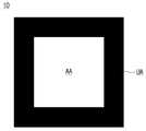
도 1은 실시예에 따른 터치 윈도우의 개략적인 평면도이다
도 2는 일 실시예에 따른 터치 윈도우의 평면도이다.
도 3은 도 2의 Ⅰ-Ⅰ’를 따라서 절단한 단면을 도시한 단면도이다.
도 4 내지 도 6은 다른 실시예에 따른 터치 윈도우의 평면도이다.
도 7은 도 6의 Ⅱ-Ⅱ’를 따라서 절단한 단면을 도시한 단면도이다.
도 8 내지 도 11은 다른 실시예에 따른 터치 윈도우의 평면도이다.
도 12는 실시예에 따른 터치 윈도우가 구동부 상에 배치된 디스플레이장치를 도시한 단면도이다.1 is a schematic plan view of a touch window according to an embodiment;
2 is a plan view of a touch window according to an exemplary embodiment.
3 is a cross-sectional view illustrating a cross section taken along the line II ′ of FIG. 2.
4 to 6 are plan views of touch windows according to other exemplary embodiments.
FIG. 7 is a cross-sectional view taken along the line II-II ′ of FIG. 6.
8 through 11 are plan views of touch windows according to other exemplary embodiments.
12 is a cross-sectional view illustrating a display apparatus in which a touch window is disposed on a driving unit, according to an exemplary embodiment.
실시예들의 설명에 있어서, 각 층(막), 영역, 패턴 또는 구조물들이 기판, 각 층(막), 영역, 패드 또는 패턴들의 “상/위(on)”에 또는 “하/아래(under)”에 형성된다는 기재는, 직접(directly) 또는 다른 층을 개재하여 형성되는 것을 모두 포함한다. 각 층의 상/위 또는 하/아래에 대한 기준은 도면을 기준으로 설명한다.In the description of embodiments, each layer, region, pattern, or structure may be “on” or “under” the substrate, each layer, region, pad, or pattern. Substrate formed in ”includes all formed directly or through another layer. Criteria for the top / bottom or bottom / bottom of each layer are described with reference to the drawings.
도면에서 각 층(막), 영역, 패턴 또는 구조물들의 두께나 크기는 설명의 명확성 및 편의를 위하여 변형될 수 있으므로, 실제 크기를 전적으로 반영하는 것은 아니다.In the drawings, the thickness or size of each layer (film), region, pattern, or structure may be modified for clarity and convenience of description, and thus do not necessarily reflect the actual size.
이하, 첨부한 도면을 참조하여 본 발명의 실시예를 상세하게 설명하면 다음과 같다.Hereinafter, exemplary embodiments of the present invention will be described in detail with reference to the accompanying drawings.
도 1 내지 도 3을 참조하여, 일 실시예에 따른 터치 윈도우를 상세하게 설명한다. 도 1은 실시예에 따른 터치 윈도우의 개략적인 평면도이다. 도 2는 제1 실시예에 따른 터치 윈도우의 평면도이다. 도 3은 도 2의 Ⅰ-Ⅰ’를 따라서 절단한 단면을 도시한 단면도이다.1 to 3, a touch window according to an embodiment will be described in detail. 1 is a schematic plan view of a touch window according to an embodiment. 2 is a plan view of a touch window according to a first embodiment. 3 is a cross-sectional view illustrating a cross section taken along line II ′ of FIG. 2.
도 1 및 도 2를 참조하면, 실시예에 따른 터치 윈도우(10)는 입력 장치(예를 들어, 손가락 등)의 위치를 감지하는 유효 영역(AA)과 이 유효 영역(AA)의 주위에 배치되는 비유효 영역(UA)이 정의되는 기판(100)을 포함한다.1 and 2, the
상기 기판(100)은 유리 기판, 폴리 에틸렌 테레프탈레이트(poly (ethylene terephthalate), PET) 필름 또는 수지를 포함하는 플라스틱 기판으로 형성될 수 있다. 그러나 실시예가 이에 한정되는 것은 아니고, 이 위에 감지 전극(200) 및 배선(300) 등이 형성될 수 있는 다양한 물질을 포함할 수 있다.The
상기 유효 영역(AA)에는 입력 장치를 감지할 수 있도록 감지 전극(200)이 형성될 수 있다. 도 2에서는 상기 감지 전극(200)이 바(bar)형태인 것으로 도시하였으나, 실시예가 이에 한정되는 것은 아니다. 따라서, 상기 감지 전극(200)은 손가락 등의 입력 장치가 접촉되었는지를 감지할 수 있는 다양한 형상으로 형성될 수 있다.The
상기 감지 전극(200)은 광의 투과를 방해하지 않으면서 전기가 흐를 수 있도록 투명 전도성 물질을 포함할 수 있다. 이를 위하여 감지 전극(200)은 인듐 주석 산화물(indium tin oxide), 인듐 아연 산화물(indium zinc oxide), 구리 산화물(copper oxide), 탄소 나노 튜브(carbon nano tube, CNT) 등의 다양한 물질을 포함할 수 있다.The
도 2에서는 상기 감지 전극(200)이 일 방향으로 연장되는 것으로 도시하였으나, 실시예가 이에 한정되는 것은 아니다. 따라서, 상기 감지 전극(200)은 상기 일 방향으로 연장되는 감지 전극 및 상기 일 방향과 교차하는 타 방향으로 연장되는 감지 전극의 두 종류의 감지 전극(200)으로 구성될 수 있다.In FIG. 2, the
이와 같은 터치 윈도우에 손가락 등의 입력 장치가 접촉되면, 입력 장치가 접촉된 부분에서 정전 용량의 차이가 발생하고, 이러한 차이가 발생한 부분을 접촉 위치로 검출할 수 있다.When an input device such as a finger is in contact with such a touch window, a difference in capacitance occurs in a portion where the input device contacts, and a portion where such a difference occurs may be detected as a contact position.
상기 비유효 영역(UA)에는 감지 전극(200)을 전기적으로 연결하는 배선(300)이 형성될 수 있다. 상기 배선(300)은 전기 전도성이 우수한 금속으로 이루어질 수 있다. 일례로, 이러한 배선(300)은 크롬(Cr), 니켈(Ni), 구리(Cu), 알루미늄(Al), 은(Ag), 몰리브덴(Mo) 및 이들의 합금으로 형성될 수 있다. 특히, 상기 배선(300)은 인쇄 공정으로 형성이 가능한 다양한 금속 페이스트 물질을 포함할 수 있다.The
상기 감지전극(200) 및 상기 배선(300) 사이에 보강전극(210)이 배치된다. 상기 보강전극(210)은 상기 감지전극(200)과 직접 접촉한다. 상기 보강전극(210)은 상기 배선(300)과 직접 접촉한다.The reinforcing
상기 보강전극(210)은 상기 감지전극(200)과 동일 또는 유사한 물질을 포함할 수 있다.The reinforcing
도 3을 참조하면, 상기 보강전극(210)의 두께(T2)는 상기 감지전극(200)의 두께(T1)보다 두꺼울 수 있다. 이를 통해, 상기 보강전극(210)이 상기 배선(300)과 접촉하는 면적을 충분히 확보할 수 있다. 즉, 상기 감지전극(200)이 직접 상기 배선(300)에 연결될 때에 비해, 상기 보강전극(210)을 통해 상기 감지전극(200)과 상기 배선(300)이 연결되므로 접촉면적을 향상할 수 있다. 따라서, 상기 보강전극(210)은 상기 감지전극(200)과 상기 배선(300)과의 단선을 방지하여 터치 윈도우의 전기적 특성을 향상할 수 있다. 또한, 감지전극(200)에 크랙(crack) 등이 발생하더라도, 상기 보강전극(210)을 통해 상기 배선(300)과 전기적으로 연결될 수 있어 신뢰성을 향상할 수 있다.Referring to FIG. 3, the thickness T2 of the reinforcing
상기 배선(300)의 끝단에는 전극 패드(400)가 위치한다. 이러한 전극 패드(400)는 인쇄 회로 기판과 접속될 수 있다. 구체적으로, 도면에 도시하지 않았으나, 상기 인쇄 회로 기판의 어느 일면에는 접속 단자가 위치하고, 상기 전극 패드(400)는 상기 접속 단자와 접속될 수 있다. 상기 전극 패드(400)는 상기 접속 단자와 대응되는 크기로 형성될 수 있다.The
상기 인쇄 회로 기판으로는 다양한 형태의 인쇄 회로 기판이 적용될 수 있는데, 일례로 플렉서블 인쇄 회로 기판(flexible printed circuit board, FPCB) 등이 적용될 수 있다.Various types of printed circuit boards may be applied to the printed circuit board. For example, a flexible printed circuit board (FPCB) may be applied.
이하, 도 4 내지 도 8을 참조하여, 다른 실시예에 따른 터치 윈도우를 설명한다. 명확하고 간략한 설명을 위해 앞서 설명한 부분과 동일 또는 유사한 부분에 대해서는 상세한 설명을 생략한다.Hereinafter, a touch window according to another exemplary embodiment will be described with reference to FIGS. 4 to 8. For the sake of clarity and simplicity, detailed description of parts identical or similar to those described above will be omitted.
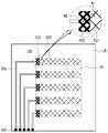
먼저, 도 4를 참조하면, 다른 실시예에 따른 터치 윈도우의 감지전극(201)은 제1 패턴(P11)을 포함하고, 보강전극(211)은 상기 제1 패턴(P11)과 다른 제2 패턴(P12)을 포함한다. 즉, 상기 감지전극(201) 및 상기 보강전극(211)을 이루는 패턴이 서로 다를 수 있다.First, referring to FIG. 4, the
구체적으로, 상기 제1 패턴(P11) 및 상기 제2 패턴(P12)은 메쉬를 포함할 수 있다. 이때, 도 4에 도시한 바와 같이, 상기 제2 패턴(P12)에 포함되는 메쉬 선의 밀도가 상기 제1 패턴(P11)에 포함되는 메쉬 선의 밀도보다 더 크다. 즉, 동일한 면적에서, 상기 제2 패턴(P12)을 이루는 메쉬 선의 개수가 상기 제1 패턴(P11)을 이루는 메쉬 선의 개수보다 많다. 일례로, 동일한 면적에서, 상기 제2 패턴(P12)을 이루는 메쉬 선의 개수가 상기 제1 패턴(P11)을 이루는 메쉬 선의 개수보다 두 배 이상 많을 수 있다. 따라서, 이러한 보강전극(211)을 통해 배선(301)과 접촉하는 메쉬 선의 개수를 많게 하여 상기 감지전극(201)과 상기 배선(301)과의 단선을 방지할 수 있다. 또한, 상기 보강전극(211)을 통해 상기 감지전극(201)과 상기 배선(301) 사이의 급격한 밀도 변화를 완충할 수 있다. 따라서, 전기적 특성이 개선될 수 있다.In detail, the first pattern P11 and the second pattern P12 may include a mesh. In this case, as shown in FIG. 4, the density of the mesh line included in the second pattern P12 is greater than the density of the mesh line included in the first pattern P11. That is, in the same area, the number of mesh lines constituting the second pattern P12 is greater than the number of mesh lines constituting the first pattern P11. For example, in the same area, the number of mesh lines constituting the second pattern P12 may be twice or more than the number of mesh lines constituting the first pattern P11. Accordingly, disconnection between the
한편, 상기 감지전극(201)이 메쉬 형상을 가짐으로써, 유효 영역(AA) 상에서 상기 감지전극(201)의 패턴이 보이지 않게 할 수 있다. 즉, 상기 감지전극(201)이 금속으로 형성되어도, 패턴이 보이지 않게 할 수 있다. 또한, 상기 감지전극(201)이 대형 크기의 터치 윈도우에 적용되어도 낮은 저항을 확보할 수 있다.Meanwhile, since the
도 5를 참조하면, 다른 실시예에 따른 터치 윈도우는 제1 패턴(P21)의 감지전극(202) 및 제2 패턴(P22)의 보강전극(212)을 포함하고, 상기 제1 패턴(P21)에 포함되는 메쉬 선과 상기 제2 패턴(P22)에 포함되는 메쉬 선의 선폭이 서로 다르게 구비된다. 구체적으로, 상기 제2 패턴(P22)에 포함되는 메쉬 선의 선폭(W2)은 상기 제1 패턴(P21)에 포함되는 메쉬 선의 선폭(W1)보다 더 넓다.Referring to FIG. 5, the touch window according to another embodiment includes a
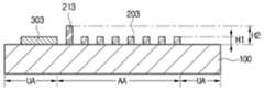
도 6 및 도 7을 참조하면, 다른 실시예에 따른 터치 윈도우는 제1 패턴(P31)의 감지전극(203) 및 제2 패턴(P32)의 보강전극(213)을 포함하고, 상기 제1 패턴(P31)에 포함되는 메쉬 선과 상기 제2 패턴(P32)에 포함되는 메쉬 선의 두께가 서로 다르게 구비된다. 구체적으로, 상기 제2 패턴(P32)에 포함되는 메쉬 선의 두께(H2)는 상기 제1 패턴(P31)에 포함되는 메쉬 선의 두께(H1)보다 더 두껍다. 한편, 상기 제1 패턴(P31)과 상기 제2 패턴(P32)의 패턴 형상은 동일하되, 선의 두께만 다를 수 있다.6 and 7, the touch window according to another embodiment includes a
도 8을 참조하면, 다른 실시예에 따른 터치 윈도우는 제1 패턴(P51)을 포함하는 감지전극(205) 및 제2 패턴(P52)을 포함하는 보강전극(215)을 포함하고, 상기 제2 패턴(P52)에 포함되는 메쉬 선의 간격(pitch)(D2)과 상기 제1 패턴(P51)에 포함되는 메쉬 선의 간격(D1)이 서로 다르게 구비된다. 구체적으로, 상기 제2 패턴(P52)에 포함되는 메쉬 선의 간격(D2)이 상기 제1 패턴(P51)에 포함되는 메쉬 선의 간격(D1)보다 작을 수 있다. 일례로, 상기 제2 패턴(P52)에 포함되는 메쉬 선의 간격(D2)과 상기 제1 패턴(P51)에 포함되는 메쉬 선의 간격(D1)의 비가 1:1 내지 1:4일 수 있다. 이를 통해, 배선(310)과 보강전극(215)의 접촉 밀도를 향상할 수 있다. 즉, 배선(310)과 상기 제2 패턴(P52)에 포함되는 메쉬 선의 접촉 개수를 늘릴 수 있다.Referring to FIG. 8, a touch window according to another embodiment includes a
한편, 다른 실시예에 따른 터치 윈도우는 제2 패턴(P52)에 포함되는 메쉬 선의 선폭(W4)과 제1 패턴(P51)에 포함되는 메쉬 선의 선폭(W3)이 동일할 수 있다. 이를 통해, 배선(301)과 감지전극(205) 사이의 선폭 변화를 상쇄할 수 있다. 따라서, 배선(301)과 감지전극(205) 사이의 밀도 및 디자인 변화에 따른 단선, 크랙(crack) 및 특성 변화를 감소시킬 수 있다.Meanwhile, in the touch window according to another exemplary embodiment, the line width W4 of the mesh line included in the second pattern P52 and the line width W3 of the mesh line included in the first pattern P51 may be the same. Through this, the line width change between the
한편, 다른 실시예에 따른 터치 윈도우는 보강전극(215)의 폭(B2)과 감지전극(205)의 폭(B1)이 서로 다르게 구비될 수 있다. 구체적으로, 상기 보강전극(215)의 폭(B2)은 감지전극(205)의 제1 패턴(P51)에 포함되는 메쉬 선의 간격(D1)의 0.3배 이상일 수 있다. 더 구체적으로, 상기 보강전극(215)의 폭(B2)은 감지전극(205)의 제1 패턴(P51)에 포함되는 메쉬 선의 간격(D1)의 0.3배보다 크고 상기 감지전극(205)의 폭(B1)보다 작을 수 있다. 바람직하게는, 상기 보강전극(215)의 폭(B2)은 감지전극(205)의 제1 패턴(P51)에 포함되는 메쉬 선의 간격(D1)의 0.5배 이상일 수 있다. 이를 통해, 배선(301)과 보강전극(215)과의 접촉 확률을 증가시킬 수 있다.Meanwhile, in the touch window according to another exemplary embodiment, the width B2 of the reinforcing
한편, 도 9를 참조하면, 다른 실시예에 따른 터치 윈도우는 보강전극(216)과 감지전극(206)의 일부가 서로 중첩될 수 있다. 즉, 상기 보강전극(216)이 상기 감지전극(206)상에 배치될 수 있다.Meanwhile, referring to FIG. 9, in the touch window according to another exemplary embodiment, a part of the reinforcing
이때, 제1 패턴(P61)을 포함하는 감지전극(206) 및 제2 패턴(P62)을 포함하는 보강전극(216)을 포함하고, 상기 제2 패턴(P62)에 포함되는 메쉬 선의 간격(pitch)(D2)과 상기 제1 패턴(P61)에 포함되는 메쉬 선의 간격(D1)이 서로 다르게 구비된다. 구체적으로, 상기 제2 패턴(P62)에 포함되는 메쉬 선의 간격(D2)이 상기 제1 패턴(P61)에 포함되는 메쉬 선의 간격(D1)보다 작을 수 있다. 일례로, 상기 제2 패턴(P62)에 포함되는 메쉬 선의 간격(D2)과 상기 제1 패턴(P61)에 포함되는 메쉬 선의 간격(D1)의 비가 1:1 내지 1:4일 수 있다. 이를 통해, 배선(310)과 보강전극(216)의 접촉 밀도를 향상할 수 있다. 즉, 배선(310)과 상기 제2 패턴(P62)에 포함되는 메쉬 선의 접촉 개수를 늘릴 수 있다.In this case, a pitch of mesh lines included in the
또한, 제2 패턴(P62)에 포함되는 메쉬 선의 선폭(W4)과 제1 패턴(P61)에 포함되는 메쉬 선의 선폭(W3)이 동일할 수 있다. 이를 통해, 배선(304)과 감지전극(206) 사이의 선폭 변화를 상쇄할 수 있다. 따라서, 배선(304)과 감지전극(206) 사이의 밀도 및 디자인 변화에 따른 단선, 크랙(crack) 및 특성 변화를 감소시킬 수 있다.In addition, the line width W4 of the mesh line included in the second pattern P62 and the line width W3 of the mesh line included in the first pattern P61 may be the same. As a result, the line width change between the
또한, 보강전극(216)의 폭(B2)과 감지전극(206)의 폭(B1)이 서로 다르게 구비될 수 있다. 구체적으로, 상기 보강전극(216)의 폭(B2)은 감지전극(206)의 제1 패턴(P61)에 포함되는 메쉬 선의 간격(D1)의 0.3배 이상일 수 있다. 더 구체적으로, 상기 보강전극(216)의 폭(B2)은 감지전극(206)의 제1 패턴(P61)에 포함되는 메쉬 선의 간격(D1)의 0.3배보다 크고 상기 감지전극(206)의 폭(B1)보다 작을 수 있다. 바람직하게는, 상기 보강전극(216)의 폭(B2)은 감지전극(206)의 제1 패턴(P61)에 포함되는 메쉬 선의 간격(D1)의 0.5배 이상일 수 있다. 이를 통해, 배선(304)과 보강전극(216)과의 접촉 확률을 증가시킬 수 있다. 도 10을 참조하면, 다른 실시예에 따른 터치 윈도우는 제3 패턴(P41)을 포함하는 감지전극(204)을 포함하고, 상기 감지전극(204)은 보강부(204a)를 포함한다. 상기 보강부(204a)는 상기 감지전극(204) 내에서 배선(304)과 인접한 영역에 배치된다. 이때, 상기 보강부(204a)는 상기 제3 패턴(P41)과 중첩되는 제4 패턴(P42)을 더 포함한다. 즉, 상기 보강부(204a)는 제3 패턴(P41) 및 제4 패턴(P42)을 포함한다. 상기 제4 패턴(P42)은 상기 제3 패턴(P41)과 상하로 접촉할 수 있다. 이때, 상기 제4 패턴(P42)과 상기 배선(304)이 접촉하는 접촉면적이 상기 제3 패턴(P41)과 상기 배선(304)이 접촉하는 접촉면적보다 크다. 즉, 상기 제4 패턴(P42)에 포함되는 선의 밀도가 더 크거나, 선의 선폭이 더 크거나, 선의 두께가 더 두꺼움으로써, 상기 제4 패턴(P42)에 포함되는 선이 상기 배선(304)과 접촉하는 접촉면적을 크게 할 수 있다.In addition, the width B2 of the reinforcing
도 11을 참조하면, 다른 실시예에 따른 터치 윈도우는 메쉬 형상의 감지전극(260)을 포함하고, 상기 감지전극(260)은 밀도가 서로 다른 적어도 두 개 이상의 영역을 포함한다.Referring to FIG. 11, a touch window according to another embodiment includes a
구체적으로, 상기 감지전극(260)은 제1 감지전극부(261) 및 제2 감지전극부(262)를 포함한다. 상기 제1 감지전극부(261)의 밀도는 상기 제2 감지전극부(262)의 밀도보다 더 크다. 일례로, 상기 제1 감지전극부(261)에 포함되는 메쉬 선의 밀도가 상기 제2 감지전극부(262)에 포함되는 메쉬 선의 밀도보다 더 클 수 있다. 따라서, 상기 제1 감지전극부(261)에 포함되는 메쉬 선의 개수가 상기 제2 감지전극부(262)에 포함되는 메쉬 선의 개수보다 더 많을 수 있다. 또한, 상기 제1 감지전극부(261)에 포함되는 메쉬 선의 선폭이 상기 제2 감지전극부(262)에 포함되는 메쉬 선의 선폭보다 더 넓을 수 있다.In detail, the
상기 제1 감지전극부(261)는 배선(305)과 직접 접촉한다. 상기 제2 감지전극부(262)는 배선(305)과 직접 접촉한다.The first
상기 제1 감지전극부(261) 및 상기 제2 감지전극부(262)를 통해 상기 배선(305)과의 접촉면적을 향상시킬 수 있고, 배선(305)과의 단선을 방지할 수 있다.The contact area with the
한편, 도 12를 참조하면 이러한 터치 윈도우는 구동부(20) 상에 배치될 수 있다. 상기 구동부(20)는 표시패널을 포함할 수 있다. 이러한 터치 윈도우 및 구동부(20)가 합착되어 디스플레이장치를 구성할 수 있다.Meanwhile, referring to FIG. 12, such a touch window may be disposed on the
상기 표시패널은 영상을 출력하기 위한 표시영역이 형성되어 있다. 이러한 디스플레이장치에 적용되는 표시패널은 일반적으로 상부기판(21) 및 하부기판(22)을 포함할 수 있다. 하부기판(22)에는 데이터라인, 게이트라인 및 박막트랜지스터(TFT) 등이 형성될 수 있다. 상부기판(21)은 하부기판(22)과 접합되어 하부기판(22) 상에 배치되는 구성요소들을 보호할 수 있다.The display panel has a display area for outputting an image. The display panel applied to such a display device may generally include an
표시패널은, 본 발명에 따른 디스플레이장치가 어떠한 종류의 디스플레이장치인지에 따라 다양한 형태로 형성될 수 있다. 즉, 본 발명에 따른 디스플레이장치는 액정표시장치(LCD), 전계방출 표시장치(Field Emission Display), 플라즈마 표시장치(PDP), 유기발광표시장치(OLED) 및 전기영동 표시장치(EPD) 등이 될 수 있으며, 이에 따라 표시패널(20)은 다양한 형태로 구성될 수 있다.The display panel may be formed in various forms according to what kind of display apparatus the display apparatus according to the present invention is. That is, the display device according to the present invention includes a liquid crystal display (LCD), a field emission display (PDP), a plasma display (PDP), an organic light emitting display (OLED) and an electrophoretic display (EPD). Accordingly, the
상술한 실시예에 설명된 특징, 구조, 효과 등은 본 발명의 적어도 하나의 실시예에 포함되며, 반드시 하나의 실시예에만 한정되는 것은 아니다. 나아가, 각 실시예에서 예시된 특징, 구조, 효과 등은 실시예들이 속하는 분야의 통상의 지식을 가지는 자에 의하여 다른 실시예들에 대해서도 조합 또는 변형되어 실시 가능하다. 따라서 이러한 조합과 변형에 관계된 내용들은 본 발명의 범위에 포함되는 것으로 해석되어야 할 것이다.Features, structures, effects, and the like described in the above embodiments are included in at least one embodiment of the present invention, and are not necessarily limited to only one embodiment. In addition, the features, structures, effects, and the like illustrated in the embodiments may be combined or modified with respect to other embodiments by those skilled in the art to which the embodiments belong. Therefore, contents related to such combinations and modifications should be construed as being included in the scope of the present invention.
또한, 이상에서 실시예들을 중심으로 설명하였으나 이는 단지 예시일 뿐 본 발명을 한정하는 것이 아니며, 본 발명이 속하는 분야의 통상의 지식을 가진 자라면 본 실시예의 본질적인 특성을 벗어나지 않는 범위에서 이상에 예시되지 않은 여러 가지의 변형과 응용이 가능함을 알 수 있을 것이다. 예를 들어, 실시예들에 구체적으로 나타난 각 구성 요소는 변형하여 실시할 수 있는 것이다. 그리고 이러한 변형과 응용에 관계된 차이점들은 첨부한 청구 범위에서 규정하는 본 발명의 범위에 포함되는 것으로 해석되어야 할 것이다.In addition, the above description has been made with reference to the embodiments, which are merely illustrative and are not intended to limit the present invention, and those skilled in the art to which the present invention pertains are described above within the scope not departing from the essential characteristics of the present embodiment. It will be appreciated that various modifications and applications are possible. For example, each component specifically shown in the embodiments may be modified. And differences relating to such modifications and applications will have to be construed as being included in the scope of the invention defined in the appended claims.
Claims (20)
Translated fromKorean상기 유효 영역 상에 배치되고, 위치를 감지하고, 일 방향으로 연장하는 복수의 감지전극들;
상기 비유효 영역 상에 배치되고, 상기 복수의 감지전극들과 전기적으로 연결되는 복수의 배선들; 및
상기 감지전극들 중 하나의 감지전극과 상기 배선들 중 하나의 배선 사이에 배치되는 보강전극을 포함하고,
상기 하나의 감지전극은 복수의 메쉬 선들을 포함하고,
상기 보강전극은 복수의 전도성 패턴들 포함하고,
상기 전도성 패턴들 중 하나의 전도성 패턴의 폭은 상기 하나의 감지 전극의 하나의 메쉬 선의 폭보다 크고,
적어도 2개의 전도성 패턴을 포함하는 상기 보강전극의 제 1 끝단은 상기 배선과 직접 접촉하고, 상기 제 1 끝단과 반대되는 제 2 끝단은 상기 감지전극의 메쉬선들과 직접 접촉하고,
상기 보강전극의 제 1 끝단에서 적어도 2개의 보강전극의 전도성 패턴들이 상기 배선과 연결되는 터치 윈도우.A substrate comprising an effective area and an invalid area;
A plurality of sensing electrodes disposed on the effective area, sensing a position, and extending in one direction;
A plurality of wires disposed on the invalid area and electrically connected to the plurality of sensing electrodes; And
A reinforcing electrode disposed between one of the sensing electrodes and one of the wirings;
The one sensing electrode includes a plurality of mesh lines,
The reinforcing electrode includes a plurality of conductive patterns,
The width of one conductive pattern of the conductive patterns is greater than the width of one mesh line of the one sensing electrode,
A first end of the reinforcing electrode including at least two conductive patterns is in direct contact with the wiring, and a second end opposite to the first end is in direct contact with mesh lines of the sensing electrode,
And a conductive pattern of at least two reinforcing electrodes connected to the wiring at the first end of the reinforcing electrode.
상기 보강전극과 상기 감지전극은 동일 물질을 포함하는 터치 윈도우.The method of claim 1,
And the reinforcing electrode and the sensing electrode include the same material.
상기 보강전극은 메쉬 선을 포함하는 터치 윈도우.The method of claim 2,
The reinforcing electrode comprises a mesh line.
상기 보강전극의 메쉬 선의 밀도가 상기 감지전극의 메쉬 선의 밀도보다 더 큰 터치 윈도우,The method of claim 3,
A touch window in which the density of the mesh line of the reinforcing electrode is greater than the density of the mesh line of the sensing electrode,
상기 보강전극은 상기 감지전극에서 상기 배선 방향으로 연장하는 터치 윈도우.The method of claim 2,
The reinforcing electrode extends in the direction of the wiring from the sensing electrode.
상기 보강전극의 메쉬 선의 두께는 상기 감지전극의 메쉬 선의 두께보다 더 두꺼운 터치 윈도우.The method of claim 3,
The thickness of the mesh line of the reinforcing electrode is thicker than the thickness of the mesh line of the sensing electrode.
상기 보강전극의 전도성 패턴의 간격(pitch)은 상기 감지전극의 메쉬 선의 간격(pitch)보다 작은 터치 윈도우.The method of claim 2,
The pitch of the conductive pattern of the reinforcing electrode is smaller than the pitch of the mesh line of the sensing electrode (pitch).
상기 보강전극의 전도성 패턴의 간격과 상기 감지전극의 메쉬 선의 간격의 비가 1:1 내지 1:4 인 터치 윈도우.The method of claim 2,
And a ratio of the distance between the conductive pattern of the reinforcing electrode and the distance between the mesh lines of the sensing electrode is 1: 1 to 1: 4.
상기 보강전극의 전도성 패턴의 선폭은 상기 감지전극의 메쉬 선의 선폭과 동일한 터치 윈도우.The method of claim 2,
The line width of the conductive pattern of the reinforcing electrode is the same as the line width of the mesh line of the sensing electrode.
상기 보강전극의 전도성 패턴의 폭은 상기 감지 전극의 메쉬 선의 간격의 0.5배 보다 큰 터치 윈도우.The method of claim 2,
The width of the conductive pattern of the reinforcing electrode is greater than 0.5 times the spacing of the mesh line of the sensing electrode.
상기 보강전극은 상기 감지전극 상에 배치되는 터치 윈도우.The method of claim 1,
The reinforcing electrode is disposed on the sensing electrode.
상기 보강전극의 두께는 상기 감지전극의 두께보다 두꺼운 터치 윈도우.The method of claim 1,
The thickness of the reinforcing electrode is thicker than the thickness of the sensing electrode.
상기 배선과 인쇄회로기판을 연결하고, 상기 비유효 영역 상에 배치되는 전극 패드를 더 포함하고,
상기 보강전극, 상기 감지전극 및 상기 배선은 서로 다른 형상으로 형성되는 터치 윈도우.The method of claim 1,
An electrode pad connecting the wiring and the printed circuit board and disposed on the invalid area;
The reinforcing electrode, the sensing electrode and the wiring are formed in different shapes.
상기 보강 전극의 제 1 끝단과 상기 제 2 끝단 사이의 폭과 상기 감지 전극의 제 1 단부와 상기 제 1 단부와 반대되는 제 2 단부 사이의 폭은 서로 다른 터치 윈도우.The method of claim 1,
And a width between the first end of the reinforcing electrode and the second end and a width between the first end of the sensing electrode and a second end opposite to the first end.
상기 보강전극의 폭은 상기 감지 전극의 메쉬 선의 간격의 0.35배 보다 큰 터치 윈도우.The method of claim 2,
The width of the reinforcing electrode is greater than 0.35 times the spacing of the mesh line of the sensing electrode.
상기 구동부 상의 터치 윈도우를 포함하고,
상기 터치 윈도우는,
유효 영역 및 비유효 영역을 포함하는 기판;
상기 유효 영역 상에 배치되고, 위치를 감지하고, 일 방향으로 연장하는 복수의 감지전극들;
상기 비유효 영역 상에 배치되고, 상기 복수의 감지전극들과 전기적으로 연결되는 복수의 배선들; 및
상기 감지 전극들 중 하나의 감지전극과 상기 배선들 중 하나의 배선 사이에 배치되는 보강전극을 포함하고,
상기 하나의 감지 전극은 복수의 메쉬 선들을 포함하고,
상기 보강 전극은 복수의 전도성 패턴들 포함하고,
상기 전도성 패턴들 중 하나의 전도성 패턴의 폭은 상기 하나의 감지 전극의 하나의 메쉬 선의 폭보다 크고,
적어도 2개의 전도성 패턴을 포함하는 상기 보강 전극의 제 1 끝단은 상기 배선과 직접 접촉하고, 상기 제 1 끝단과 반대되는 제 2 끝단은 상기 감지 전극의 메쉬선들과 직접 접촉하고,
상기 보강 전극의 제 1 끝단에서 적어도 2개의 보강 전극의 전도성 패턴들이 상기 배선과 연결되는 디스플레이.A drive unit;
A touch window on the driver;
The touch window,
A substrate comprising an effective area and an invalid area;
A plurality of sensing electrodes disposed on the effective area, sensing a position, and extending in one direction;
A plurality of wires disposed on the invalid area and electrically connected to the plurality of sensing electrodes; And
A reinforcing electrode disposed between one of the sensing electrodes and one of the wirings;
The one sensing electrode includes a plurality of mesh lines,
The reinforcing electrode comprises a plurality of conductive patterns,
The width of one conductive pattern of the conductive patterns is greater than the width of one mesh line of the one sensing electrode,
A first end of the reinforcing electrode including at least two conductive patterns is in direct contact with the wiring, and a second end opposite to the first end is in direct contact with mesh lines of the sensing electrode,
And a conductive pattern of at least two reinforcing electrodes connected to the wiring at the first end of the reinforcing electrode.
Applications Claiming Priority (2)
| Application Number | Priority Date | Filing Date | Title |
|---|---|---|---|
| KR1020130083663 | 2013-07-16 | ||
| KR20130083663 | 2013-07-16 |
Publications (2)
| Publication Number | Publication Date |
|---|---|
| KR20150009420A KR20150009420A (en) | 2015-01-26 |
| KR102053258B1true KR102053258B1 (en) | 2019-12-06 |
Family
ID=52346349
Family Applications (1)
| Application Number | Title | Priority Date | Filing Date |
|---|---|---|---|
| KR1020140003985AActiveKR102053258B1 (en) | 2013-07-16 | 2014-01-13 | Touch window |
Country Status (6)
| Country | Link |
|---|---|
| US (1) | US10156944B2 (en) |
| EP (1) | EP3000017A4 (en) |
| KR (1) | KR102053258B1 (en) |
| CN (1) | CN105453000A (en) |
| TW (1) | TWI632493B (en) |
| WO (1) | WO2015008933A1 (en) |
Families Citing this family (16)
| Publication number | Priority date | Publication date | Assignee | Title |
|---|---|---|---|---|
| BR112015016446B1 (en) | 2013-01-09 | 2019-10-29 | Basf Agro Bv | process for preparing compounds of formula ii, aqueous solution and use of aqueous solution |
| KR102222194B1 (en) | 2013-10-17 | 2021-03-04 | 엘지이노텍 주식회사 | Touch window and display with the same |
| US9720551B2 (en) | 2014-07-30 | 2017-08-01 | Lg Innotek Co., Ltd. | Touch window |
| PL3214937T3 (en) | 2014-11-07 | 2024-10-14 | Basf Se | Pesticidal mixtures |
| TWI545480B (en) | 2015-01-07 | 2016-08-11 | 群創光電股份有限公司 | Touch display apparatus |
| JP6440526B2 (en)* | 2015-02-27 | 2018-12-19 | 株式会社フジクラ | Wiring body |
| WO2016136967A1 (en)* | 2015-02-27 | 2016-09-01 | 株式会社フジクラ | Wiring body, wiring substrate, and touch sensor |
| JP2019517053A (en)* | 2016-04-05 | 2019-06-20 | スリーエム イノベイティブ プロパティズ カンパニー | Nanowire contact pad with improved adhesion to metal interconnects |
| US10884950B2 (en)* | 2016-05-16 | 2021-01-05 | International Business Machines Corporation | Importance based page replacement |
| KR101904969B1 (en) | 2016-07-29 | 2018-10-10 | 삼성디스플레이 주식회사 | Display device |
| JP6678553B2 (en)* | 2016-10-05 | 2020-04-08 | 日本航空電子工業株式会社 | Electronic device and touch panel |
| KR102420355B1 (en) | 2018-01-31 | 2022-07-13 | 엘지전자 주식회사 | Display device |
| DE102018105927B4 (en)* | 2018-03-14 | 2024-05-08 | Bcs Automotive Interface Solutions Gmbh | Touch-sensitive control element with a light source, a decorative part and a layer of several conductors in between, which has two areas of different light transmittance |
| CN117334127A (en)* | 2019-12-18 | 2024-01-02 | 群创光电股份有限公司 | Display devices and flexible devices |
| EP4105830A4 (en) | 2020-02-13 | 2023-07-19 | Asahi Kasei Kabushiki Kaisha | Transparent antenna and rf tag |
| KR102833362B1 (en)* | 2020-03-10 | 2025-07-14 | 삼성디스플레이 주식회사 | Sensing unit |
Citations (3)
| Publication number | Priority date | Publication date | Assignee | Title |
|---|---|---|---|---|
| JP2012208732A (en)* | 2011-03-30 | 2012-10-25 | Alps Electric Co Ltd | Input device |
| WO2013094729A1 (en) | 2011-12-22 | 2013-06-27 | 富士フイルム株式会社 | Conductive sheet and touch panel |
| JP2013131156A (en)* | 2011-12-22 | 2013-07-04 | Fujifilm Corp | Conductive sheet and touch panel |
Family Cites Families (32)
| Publication number | Priority date | Publication date | Assignee | Title |
|---|---|---|---|---|
| KR100393044B1 (en) | 2000-11-14 | 2003-07-31 | 삼성에스디아이 주식회사 | Touch Pannel having compensation electrode patterns for protecting wired electrodes from openning |
| US6819316B2 (en)* | 2001-04-17 | 2004-11-16 | 3M Innovative Properties Company | Flexible capacitive touch sensor |
| US8059103B2 (en)* | 2007-11-21 | 2011-11-15 | 3M Innovative Properties Company | System and method for determining touch positions based on position-dependent electrical charges |
| KR101720919B1 (en) | 2008-02-28 | 2017-03-28 | 쓰리엠 이노베이티브 프로퍼티즈 컴파니 | Touch screen sensor |
| KR100894710B1 (en)* | 2008-06-27 | 2009-04-24 | (주) 월드비젼 | Window integrated touch screen and manufacturing method thereof |
| US8726497B2 (en) | 2008-08-01 | 2014-05-20 | 3M Innovative Properties Company | Methods of making composite electrodes |
| US20120036919A1 (en)* | 2009-04-15 | 2012-02-16 | Kamins Theodore I | Nanowire sensor having a nanowire and electrically conductive film |
| GB0913734D0 (en) | 2009-08-06 | 2009-09-16 | Binstead Ronald P | Masked touch sensors |
| KR101093651B1 (en) | 2010-05-25 | 2011-12-15 | 전자부품연구원 | Touch panel using metal thin film and manufacturing method thereof |
| JP5248653B2 (en)* | 2010-05-27 | 2013-07-31 | 富士フイルム株式会社 | Conductive sheet and capacitive touch panel |
| KR101759577B1 (en)* | 2010-08-23 | 2017-07-19 | 삼성전자 주식회사 | On-cell TSP active matrix organic light emitting diode structure |
| KR20120041529A (en)* | 2010-10-21 | 2012-05-02 | 삼성전기주식회사 | Electrostatic capacity type touch-screen and manufacturing method thereof |
| US8803839B2 (en)* | 2010-10-31 | 2014-08-12 | Pixart Imaging Inc. | Capacitive coupling of a capacitive touchscreen to a printed circuit and controller |
| JP5720222B2 (en)* | 2010-12-13 | 2015-05-20 | ソニー株式会社 | Display device and electronic device |
| US8854326B2 (en)* | 2011-03-10 | 2014-10-07 | Wintek Corporation | Touch panel and touch-sensitive display device |
| KR101293179B1 (en)* | 2011-06-13 | 2013-08-16 | 엘지이노텍 주식회사 | Liquid crystal display combined touch screen |
| CN102902425B (en) | 2011-07-28 | 2016-06-08 | 宸鸿科技(厦门)有限公司 | Capacitance type touch-control panel structure and manufacture method |
| KR20130027747A (en) | 2011-09-08 | 2013-03-18 | 삼성전기주식회사 | Touch pannel |
| CN103019429A (en)* | 2011-09-23 | 2013-04-03 | 宸鸿科技(厦门)有限公司 | Touch panel and manufacturing method thereof |
| KR101357591B1 (en) | 2011-11-16 | 2014-02-04 | 엘지이노텍 주식회사 | Touch window having reinforcing pad |
| BR112014010102A8 (en)* | 2011-12-16 | 2017-06-20 | Fujifilm Corp | electroconductive sheet and touch panel |
| CN202404553U (en) | 2012-03-01 | 2012-08-29 | 祥达光学(厦门)有限公司 | Touch screen structure with shielding metal line |
| TWI489335B (en)* | 2012-08-09 | 2015-06-21 | Wistron Corp | Conductive substrate and touch panel |
| US9167688B2 (en)* | 2012-08-10 | 2015-10-20 | Eastman Kodak Company | Micro-wire pattern for electrode connection |
| KR101474064B1 (en)* | 2012-09-11 | 2014-12-17 | 엘지디스플레이 주식회사 | Touch screen panel for display device |
| CN202948423U (en) | 2012-11-09 | 2013-05-22 | 宝宸(厦门)光学科技有限公司 | Touch control induction electrode structure |
| US9268446B2 (en)* | 2013-02-06 | 2016-02-23 | Nanchang O-Film Tech. Co., Ltd. | Monitor, touchscreen sensing module thereof, and method for manufacturing the touchscreen sensing module |
| CN103105970B (en)* | 2013-02-06 | 2014-09-17 | 南昌欧菲光科技有限公司 | Touch screen induction module and display comprising same |
| US9201551B2 (en)* | 2013-03-28 | 2015-12-01 | Nanchang O-Film Tech. Co., Ltd. | Capacitive touch screen |
| US9066426B2 (en)* | 2013-03-28 | 2015-06-23 | Nanchang O-Film Tech. Co., Ltd. | Transparent conductive film |
| TWI478024B (en) | 2013-05-31 | 2015-03-21 | Eturbo Touch Technology Inc | Touch panel and the touch panel making method |
| TWM476977U (en) | 2013-06-13 | 2014-04-21 | Wintek Corp | Touch panel |
- 2014
- 2014-01-13KRKR1020140003985Apatent/KR102053258B1/enactiveActive
- 2014-06-10CNCN201480040869.7Apatent/CN105453000A/enactivePending
- 2014-06-10USUS14/904,410patent/US10156944B2/enactiveActive
- 2014-06-10EPEP14825937.7Apatent/EP3000017A4/ennot_activeCeased
- 2014-06-10WOPCT/KR2014/005085patent/WO2015008933A1/enactiveApplication Filing
- 2014-06-13TWTW103120585Apatent/TWI632493B/enactive
Patent Citations (3)
| Publication number | Priority date | Publication date | Assignee | Title |
|---|---|---|---|---|
| JP2012208732A (en)* | 2011-03-30 | 2012-10-25 | Alps Electric Co Ltd | Input device |
| WO2013094729A1 (en) | 2011-12-22 | 2013-06-27 | 富士フイルム株式会社 | Conductive sheet and touch panel |
| JP2013131156A (en)* | 2011-12-22 | 2013-07-04 | Fujifilm Corp | Conductive sheet and touch panel |
Also Published As
| Publication number | Publication date |
|---|---|
| EP3000017A4 (en) | 2017-01-25 |
| TWI632493B (en) | 2018-08-11 |
| TW201512933A (en) | 2015-04-01 |
| US20160147337A1 (en) | 2016-05-26 |
| US10156944B2 (en) | 2018-12-18 |
| EP3000017A1 (en) | 2016-03-30 |
| CN105453000A (en) | 2016-03-30 |
| KR20150009420A (en) | 2015-01-26 |
| WO2015008933A1 (en) | 2015-01-22 |
Similar Documents
| Publication | Publication Date | Title |
|---|---|---|
| KR102053258B1 (en) | Touch window | |
| KR102222194B1 (en) | Touch window and display with the same | |
| KR102108846B1 (en) | Touch window | |
| KR102262548B1 (en) | Touch window | |
| KR102241773B1 (en) | Touch sensor device | |
| KR102187680B1 (en) | Touch window | |
| KR102262530B1 (en) | Touch window and display with the same | |
| JP5374457B2 (en) | Planar body and touch panel | |
| KR20180025389A (en) | Touch panel and display device including the same | |
| KR102335116B1 (en) | Touch screen pannel and manufacturing method thereof | |
| KR20150036903A (en) | Touch window and display with the same | |
| KR20150103601A (en) | Touch panel | |
| TWI630517B (en) | Touch window and touch device including the same | |
| KR102262553B1 (en) | Touch panel | |
| CN105874410B (en) | Touch window and display device including the touch window | |
| KR102098383B1 (en) | Touch window and method of the same | |
| KR102131192B1 (en) | Touch window and display with the same | |
| KR102237964B1 (en) | Electrod members, touch window with the same and display with the same | |
| KR102302818B1 (en) | Touch window and display with the same | |
| KR102131177B1 (en) | Touch window and display with the same | |
| KR102119834B1 (en) | Touch window and display with the same | |
| KR102199333B1 (en) | Touch window | |
| KR20150007715A (en) | Touch window | |
| KR102098389B1 (en) | Touch window and display with the same | |
| KR102288796B1 (en) | Touch window |
Legal Events
| Date | Code | Title | Description |
|---|---|---|---|
| PA0109 | Patent application | Patent event code:PA01091R01D Comment text:Patent Application Patent event date:20140113 | |
| PG1501 | Laying open of application | ||
| A201 | Request for examination | ||
| PA0201 | Request for examination | Patent event code:PA02012R01D Patent event date:20180524 Comment text:Request for Examination of Application Patent event code:PA02011R01I Patent event date:20140113 Comment text:Patent Application | |
| E902 | Notification of reason for refusal | ||
| PE0902 | Notice of grounds for rejection | Comment text:Notification of reason for refusal Patent event date:20190529 Patent event code:PE09021S01D | |
| E701 | Decision to grant or registration of patent right | ||
| PE0701 | Decision of registration | Patent event code:PE07011S01D Comment text:Decision to Grant Registration Patent event date:20191126 | |
| GRNT | Written decision to grant | ||
| PR0701 | Registration of establishment | Comment text:Registration of Establishment Patent event date:20191202 Patent event code:PR07011E01D | |
| PR1002 | Payment of registration fee | Payment date:20191203 End annual number:3 Start annual number:1 | |
| PG1601 | Publication of registration | ||
| PR1001 | Payment of annual fee | Payment date:20221114 Start annual number:4 End annual number:4 | |
| PR1001 | Payment of annual fee | Payment date:20231113 Start annual number:5 End annual number:5 | |
| PR1001 | Payment of annual fee | Payment date:20241118 Start annual number:6 End annual number:6 |