KR102044923B1 - Organic light emitting display device and manufacturing method thereof - Google Patents
Organic light emitting display device and manufacturing method thereofDownload PDFInfo
- Publication number
- KR102044923B1 KR102044923B1KR1020130040926AKR20130040926AKR102044923B1KR 102044923 B1KR102044923 B1KR 102044923B1KR 1020130040926 AKR1020130040926 AKR 1020130040926AKR 20130040926 AKR20130040926 AKR 20130040926AKR 102044923 B1KR102044923 B1KR 102044923B1
- Authority
- KR
- South Korea
- Prior art keywords
- organic
- layer
- organic film
- film
- light emitting
- Prior art date
- Legal status (The legal status is an assumption and is not a legal conclusion. Google has not performed a legal analysis and makes no representation as to the accuracy of the status listed.)
- Active
Links
- 238000004519manufacturing processMethods0.000titleclaimsdescription15
- 239000010410layerSubstances0.000claimsabstractdescription109
- 239000012044organic layerSubstances0.000claimsabstractdescription96
- 238000005538encapsulationMethods0.000claimsabstractdescription31
- 239000000758substrateSubstances0.000claimsabstractdescription26
- 239000000463materialSubstances0.000claimsdescription22
- 238000000034methodMethods0.000claimsdescription21
- 230000001678irradiating effectEffects0.000claimsdescription3
- 239000011368organic materialSubstances0.000abstractdescription27
- 239000011159matrix materialSubstances0.000abstractdescription21
- 239000010408filmSubstances0.000description62
- 238000009826distributionMethods0.000description8
- 239000010409thin filmSubstances0.000description8
- 238000000605extractionMethods0.000description6
- 239000011347resinSubstances0.000description6
- 229920005989resinPolymers0.000description6
- 238000010586diagramMethods0.000description4
- 238000002347injectionMethods0.000description4
- 239000007924injectionSubstances0.000description4
- 230000001788irregularEffects0.000description4
- XEEYBQQBJWHFJM-UHFFFAOYSA-NIronChemical compound[Fe]XEEYBQQBJWHFJM-UHFFFAOYSA-N0.000description3
- PXHVJJICTQNCMI-UHFFFAOYSA-NNickelChemical compound[Ni]PXHVJJICTQNCMI-UHFFFAOYSA-N0.000description3
- KDLHZDBZIXYQEI-UHFFFAOYSA-NPalladiumChemical compound[Pd]KDLHZDBZIXYQEI-UHFFFAOYSA-N0.000description3
- AMGQUBHHOARCQH-UHFFFAOYSA-Nindium;oxotinChemical compound[In].[Sn]=OAMGQUBHHOARCQH-UHFFFAOYSA-N0.000description3
- BASFCYQUMIYNBI-UHFFFAOYSA-NplatinumChemical compound[Pt]BASFCYQUMIYNBI-UHFFFAOYSA-N0.000description3
- 230000005855radiationEffects0.000description3
- YVTHLONGBIQYBO-UHFFFAOYSA-Nzinc indium(3+) oxygen(2-)Chemical compound[O--].[Zn++].[In+3]YVTHLONGBIQYBO-UHFFFAOYSA-N0.000description3
- 239000004925Acrylic resinSubstances0.000description2
- XLOMVQKBTHCTTD-UHFFFAOYSA-NZinc monoxideChemical compound[Zn]=OXLOMVQKBTHCTTD-UHFFFAOYSA-N0.000description2
- 239000011575calciumSubstances0.000description2
- 238000005229chemical vapour depositionMethods0.000description2
- 239000011651chromiumSubstances0.000description2
- 150000001875compoundsChemical class0.000description2
- 239000010949copperSubstances0.000description2
- 239000010931goldSubstances0.000description2
- 239000011777magnesiumSubstances0.000description2
- 238000012986modificationMethods0.000description2
- 230000004048modificationEffects0.000description2
- -1polyethylene terephthalatePolymers0.000description2
- VYPSYNLAJGMNEJ-UHFFFAOYSA-Nsilicon dioxideInorganic materialsO=[Si]=OVYPSYNLAJGMNEJ-UHFFFAOYSA-N0.000description2
- 239000010936titaniumSubstances0.000description2
- NIXOWILDQLNWCW-UHFFFAOYSA-MAcrylateChemical compound[O-]C(=O)C=CNIXOWILDQLNWCW-UHFFFAOYSA-M0.000description1
- 229920000178Acrylic resinPolymers0.000description1
- LSNNMFCWUKXFEE-UHFFFAOYSA-MBisulfiteChemical compoundOS([O-])=OLSNNMFCWUKXFEE-UHFFFAOYSA-M0.000description1
- OYPRJOBELJOOCE-UHFFFAOYSA-NCalciumChemical compound[Ca]OYPRJOBELJOOCE-UHFFFAOYSA-N0.000description1
- VYZAMTAEIAYCRO-UHFFFAOYSA-NChromiumChemical compound[Cr]VYZAMTAEIAYCRO-UHFFFAOYSA-N0.000description1
- RYGMFSIKBFXOCR-UHFFFAOYSA-NCopperChemical compound[Cu]RYGMFSIKBFXOCR-UHFFFAOYSA-N0.000description1
- 239000004593EpoxySubstances0.000description1
- WHXSMMKQMYFTQS-UHFFFAOYSA-NLithiumChemical compound[Li]WHXSMMKQMYFTQS-UHFFFAOYSA-N0.000description1
- FYYHWMGAXLPEAU-UHFFFAOYSA-NMagnesiumChemical compound[Mg]FYYHWMGAXLPEAU-UHFFFAOYSA-N0.000description1
- ZOKXTWBITQBERF-UHFFFAOYSA-NMolybdenumChemical compound[Mo]ZOKXTWBITQBERF-UHFFFAOYSA-N0.000description1
- 239000004721Polyphenylene oxideSubstances0.000description1
- 229920002396PolyureaPolymers0.000description1
- 229910052581Si3N4Inorganic materials0.000description1
- GWEVSGVZZGPLCZ-UHFFFAOYSA-NTitan oxideChemical compoundO=[Ti]=OGWEVSGVZZGPLCZ-UHFFFAOYSA-N0.000description1
- RTAQQCXQSZGOHL-UHFFFAOYSA-NTitaniumChemical compound[Ti]RTAQQCXQSZGOHL-UHFFFAOYSA-N0.000description1
- NRTOMJZYCJJWKI-UHFFFAOYSA-NTitanium nitrideChemical compound[Ti]#NNRTOMJZYCJJWKI-UHFFFAOYSA-N0.000description1
- 229910052783alkali metalInorganic materials0.000description1
- 150000001340alkali metalsChemical class0.000description1
- 229910052784alkaline earth metalInorganic materials0.000description1
- 150000001342alkaline earth metalsChemical class0.000description1
- 238000000231atomic layer depositionMethods0.000description1
- WKDNYTOXBCRNPV-UHFFFAOYSA-NbpdaChemical compoundC1=C2C(=O)OC(=O)C2=CC(C=2C=C3C(=O)OC(C3=CC=2)=O)=C1WKDNYTOXBCRNPV-UHFFFAOYSA-N0.000description1
- 229910052792caesiumInorganic materials0.000description1
- TVFDJXOCXUVLDH-UHFFFAOYSA-Ncaesium atomChemical compound[Cs]TVFDJXOCXUVLDH-UHFFFAOYSA-N0.000description1
- 229910052791calciumInorganic materials0.000description1
- 229910052804chromiumInorganic materials0.000description1
- 229910017052cobaltInorganic materials0.000description1
- 239000010941cobaltSubstances0.000description1
- GUTLYIVDDKVIGB-UHFFFAOYSA-Ncobalt atomChemical compound[Co]GUTLYIVDDKVIGB-UHFFFAOYSA-N0.000description1
- 229910052802copperInorganic materials0.000description1
- PMHQVHHXPFUNSP-UHFFFAOYSA-Mcopper(1+);methylsulfanylmethane;bromideChemical compoundBr[Cu].CSCPMHQVHHXPFUNSP-UHFFFAOYSA-M0.000description1
- UHESRSKEBRADOO-UHFFFAOYSA-Nethyl carbamate;prop-2-enoic acidChemical compoundOC(=O)C=C.CCOC(N)=OUHESRSKEBRADOO-UHFFFAOYSA-N0.000description1
- ANSXAPJVJOKRDJ-UHFFFAOYSA-Nfuro[3,4-f][2]benzofuran-1,3,5,7-tetroneChemical compoundC1=C2C(=O)OC(=O)C2=CC2=C1C(=O)OC2=OANSXAPJVJOKRDJ-UHFFFAOYSA-N0.000description1
- 239000011521glassSubstances0.000description1
- PCHJSUWPFVWCPO-UHFFFAOYSA-NgoldChemical compound[Au]PCHJSUWPFVWCPO-UHFFFAOYSA-N0.000description1
- 229910052737goldInorganic materials0.000description1
- 230000005283ground stateEffects0.000description1
- 229910052735hafniumInorganic materials0.000description1
- 229910052738indiumInorganic materials0.000description1
- APFVFJFRJDLVQX-UHFFFAOYSA-Nindium atomChemical compound[In]APFVFJFRJDLVQX-UHFFFAOYSA-N0.000description1
- 239000011810insulating materialSubstances0.000description1
- 238000000025interference lithographyMethods0.000description1
- 229910052742ironInorganic materials0.000description1
- 238000010030laminatingMethods0.000description1
- 238000003475laminationMethods0.000description1
- 239000004973liquid crystal related substanceSubstances0.000description1
- 229910052744lithiumInorganic materials0.000description1
- 238000001459lithographyMethods0.000description1
- 229910052749magnesiumInorganic materials0.000description1
- 229910052750molybdenumInorganic materials0.000description1
- 239000011733molybdenumSubstances0.000description1
- 229910052759nickelInorganic materials0.000description1
- 230000003287optical effectEffects0.000description1
- TWNQGVIAIRXVLR-UHFFFAOYSA-Noxo(oxoalumanyloxy)alumaneChemical compoundO=[Al]O[Al]=OTWNQGVIAIRXVLR-UHFFFAOYSA-N0.000description1
- 229910052763palladiumInorganic materials0.000description1
- CLYVDMAATCIVBF-UHFFFAOYSA-Npigment red 224Chemical compoundC=12C3=CC=C(C(OC4=O)=O)C2=C4C=CC=1C1=CC=C2C(=O)OC(=O)C4=CC=C3C1=C42CLYVDMAATCIVBF-UHFFFAOYSA-N0.000description1
- 238000000623plasma-assisted chemical vapour depositionMethods0.000description1
- 229910052697platinumInorganic materials0.000description1
- 229920000058polyacrylatePolymers0.000description1
- 229920005668polycarbonate resinPolymers0.000description1
- 239000004431polycarbonate resinSubstances0.000description1
- 229920000570polyetherPolymers0.000description1
- 229920000139polyethylene terephthalatePolymers0.000description1
- 239000005020polyethylene terephthalateSubstances0.000description1
- 229920001721polyimidePolymers0.000description1
- 239000009719polyimide resinSubstances0.000description1
- 238000006116polymerization reactionMethods0.000description1
- 239000010453quartzSubstances0.000description1
- 230000002787reinforcementEffects0.000description1
- HQVNEWCFYHHQES-UHFFFAOYSA-Nsilicon nitrideChemical compoundN12[Si]34N5[Si]62N3[Si]51N64HQVNEWCFYHHQES-UHFFFAOYSA-N0.000description1
- 229910052814silicon oxideInorganic materials0.000description1
- 229910052712strontiumInorganic materials0.000description1
- CIOAGBVUUVVLOB-UHFFFAOYSA-Nstrontium atomChemical compound[Sr]CIOAGBVUUVVLOB-UHFFFAOYSA-N0.000description1
- MZLGASXMSKOWSE-UHFFFAOYSA-Ntantalum nitrideChemical compound[Ta]#NMZLGASXMSKOWSE-UHFFFAOYSA-N0.000description1
- 229910052719titaniumInorganic materials0.000description1
- OGIDPMRJRNCKJF-UHFFFAOYSA-Ntitanium oxideInorganic materials[Ti]=OOGIDPMRJRNCKJF-UHFFFAOYSA-N0.000description1
- 239000012780transparent materialSubstances0.000description1
- WFKWXMTUELFFGS-UHFFFAOYSA-NtungstenChemical compound[W]WFKWXMTUELFFGS-UHFFFAOYSA-N0.000description1
- 229910052721tungstenInorganic materials0.000description1
- 239000010937tungstenSubstances0.000description1
- 238000009281ultraviolet germicidal irradiationMethods0.000description1
- 238000001771vacuum depositionMethods0.000description1
- 239000011787zinc oxideSubstances0.000description1
- ZVWKZXLXHLZXLS-UHFFFAOYSA-Nzirconium nitrideChemical compound[Zr]#NZVWKZXLXHLZXLS-UHFFFAOYSA-N0.000description1
Images


Classifications
- H—ELECTRICITY
- H10—SEMICONDUCTOR DEVICES; ELECTRIC SOLID-STATE DEVICES NOT OTHERWISE PROVIDED FOR
- H10K—ORGANIC ELECTRIC SOLID-STATE DEVICES
- H10K59/00—Integrated devices, or assemblies of multiple devices, comprising at least one organic light-emitting element covered by group H10K50/00
- H10K59/10—OLED displays
- H10K59/12—Active-matrix OLED [AMOLED] displays
- H10K59/125—Active-matrix OLED [AMOLED] displays including organic TFTs [OTFT]
- H—ELECTRICITY
- H10—SEMICONDUCTOR DEVICES; ELECTRIC SOLID-STATE DEVICES NOT OTHERWISE PROVIDED FOR
- H10K—ORGANIC ELECTRIC SOLID-STATE DEVICES
- H10K59/00—Integrated devices, or assemblies of multiple devices, comprising at least one organic light-emitting element covered by group H10K50/00
- H10K59/80—Constructional details
- H10K59/875—Arrangements for extracting light from the devices
- H10K59/879—Arrangements for extracting light from the devices comprising refractive means, e.g. lenses
- H—ELECTRICITY
- H05—ELECTRIC TECHNIQUES NOT OTHERWISE PROVIDED FOR
- H05B—ELECTRIC HEATING; ELECTRIC LIGHT SOURCES NOT OTHERWISE PROVIDED FOR; CIRCUIT ARRANGEMENTS FOR ELECTRIC LIGHT SOURCES, IN GENERAL
- H05B33/00—Electroluminescent light sources
- H05B33/10—Apparatus or processes specially adapted to the manufacture of electroluminescent light sources
- H—ELECTRICITY
- H10—SEMICONDUCTOR DEVICES; ELECTRIC SOLID-STATE DEVICES NOT OTHERWISE PROVIDED FOR
- H10K—ORGANIC ELECTRIC SOLID-STATE DEVICES
- H10K50/00—Organic light-emitting devices
- H10K50/80—Constructional details
- H10K50/85—Arrangements for extracting light from the devices
- H10K50/854—Arrangements for extracting light from the devices comprising scattering means
- H—ELECTRICITY
- H10—SEMICONDUCTOR DEVICES; ELECTRIC SOLID-STATE DEVICES NOT OTHERWISE PROVIDED FOR
- H10K—ORGANIC ELECTRIC SOLID-STATE DEVICES
- H10K50/00—Organic light-emitting devices
- H10K50/80—Constructional details
- H10K50/85—Arrangements for extracting light from the devices
- H10K50/858—Arrangements for extracting light from the devices comprising refractive means, e.g. lenses
- H—ELECTRICITY
- H10—SEMICONDUCTOR DEVICES; ELECTRIC SOLID-STATE DEVICES NOT OTHERWISE PROVIDED FOR
- H10K—ORGANIC ELECTRIC SOLID-STATE DEVICES
- H10K59/00—Integrated devices, or assemblies of multiple devices, comprising at least one organic light-emitting element covered by group H10K50/00
- H10K59/10—OLED displays
- H10K59/12—Active-matrix OLED [AMOLED] displays
- H10K59/126—Shielding, e.g. light-blocking means over the TFTs
- H—ELECTRICITY
- H10—SEMICONDUCTOR DEVICES; ELECTRIC SOLID-STATE DEVICES NOT OTHERWISE PROVIDED FOR
- H10K—ORGANIC ELECTRIC SOLID-STATE DEVICES
- H10K59/00—Integrated devices, or assemblies of multiple devices, comprising at least one organic light-emitting element covered by group H10K50/00
- H10K59/80—Constructional details
- H10K59/875—Arrangements for extracting light from the devices
- H10K59/877—Arrangements for extracting light from the devices comprising scattering means
Landscapes
- Engineering & Computer Science (AREA)
- Physics & Mathematics (AREA)
- Optics & Photonics (AREA)
- Microelectronics & Electronic Packaging (AREA)
- Manufacturing & Machinery (AREA)
- Electroluminescent Light Sources (AREA)
Abstract
Translated fromKoreanDescription
Translated fromKorean본 발명은 유기발광 표시장치 및 그의 제조방법에 관한 것으로, 보다 상세하게는, 박막 봉지층에 패턴화 유기막을 배치시켜 광 추출 효율을 높이도록 한 유기발광 표시장치 및 그의 제조방법에 관한 것이다.The present invention relates to an organic light emitting display device and a method for manufacturing the same, and more particularly, to an organic light emitting display device and a method of manufacturing the same by placing a patterned organic film on a thin film encapsulation layer to increase light extraction efficiency.
유기발광 표시장치(Organic Light Emitting Display Device)는 빛을 방출하는 유기발광소자(Organic Light Emitting Diode)를 가지고 화상을 표시하는 자발광형 표시 장치이다. 유기발광 표시장치는 액정표시장치(Liquid Crystal Display)와는 달리 별도의 광원을 필요로 하지 않기 때문에 상대적으로 두께와 무게를 줄일 수 있고, 소비전력이 낮고, 휘도가 높으며, 반응속도가 빠르다는 장점이 있다.An organic light emitting display device is a self-luminous display that displays an image with an organic light emitting diode that emits light. Unlike liquid crystal displays, organic light-emitting displays do not require a separate light source, so they can be reduced in thickness and weight, have low power consumption, high luminance, and fast response speed. have.
상기 유기발광 표시장치는 정공 주입 전극, 유기 발광층, 전자주입 전극 및 박막 봉지층을 갖는다. 유기 발광 소자는 정공 주입 전극으로부터 공급받은 정공과 전자 주입 전극으로부터 공급받은 전자가 유기 발광층 내에서 결합하여 형성된 여기자(exciton)가 기저상태로 떨어질 때 발생되는 에너지에 의해 빛을 발생한다.The organic light emitting diode display includes a hole injection electrode, an organic emission layer, an electron injection electrode, and a thin film encapsulation layer. The organic light emitting device generates light by energy generated when an exciton formed by combining holes supplied from the hole injection electrode and electrons supplied from the electron injection electrode in the organic emission layer falls to the ground state.
상기 유기발광 표시장치에 포함된 각 층은 서로 다른 물질로 이루어지므로 각각 굴절률 차가 생긴다. 상기 각 층의 굴절률 차로 인하여 상기 유기발광 표시장치 내부에서는 전반사가 일어나고, 상기 유기 발광층에서 발생한 빛의 일부가 상기 내부 전반사로 인하여 구속되어 소멸되는 문제점이 있었다.Each layer included in the organic light emitting display device is made of a different material, and thus there is a difference in refractive index. Due to the difference in refractive index of each layer, total internal reflection occurs inside the organic light emitting display device, and a part of the light generated in the organic light emitting layer is constrained and extinguished due to the total internal reflection.
본 발명의 일례에서는 봉지층에 패턴화 유기막을 형성하여 유기발광 표시장치 내부에 발생하는 전반사를 줄임으로써 광 추출 효율이 향상된 유기발광 표시장치 및 그 제조방법을 제안하고자 한다.In an exemplary embodiment of the present invention, an organic light emitting display device having improved light extraction efficiency and a method of manufacturing the same may be proposed by forming a patterned organic layer on an encapsulation layer to reduce total reflection occurring inside the organic light emitting display device.
본 발명의 일예에서는 기판; 상기 기판상에 형성된 표시부; 및 상기 표시부상에 형성된 봉지층;을 포함하며, 상기 봉지층은 복수개의 무기막 및 복수개의 유기막을 포함하고, 상기 복수개의 무기막과 상기 복수개의 유기막은 교대로 적층되어 형성되고, 상기 복수개의 유기막 중 적어도 하나는 패턴화 유기막이고, 상기 패턴화 유기막은 유기물질로 된 매트릭스에 복수개의 고굴절률 부분이 산재하는 구조인 것을 특징으로 하는 유기발광 표시장치를 제공한다.In one embodiment of the present invention; A display unit formed on the substrate; And an encapsulation layer formed on the display unit, wherein the encapsulation layer includes a plurality of inorganic layers and a plurality of organic layers, wherein the plurality of inorganic layers and the plurality of organic layers are alternately stacked. At least one of the organic layers may be a patterned organic layer, and the patterned organic layer may have a structure in which a plurality of high refractive index portions are interspersed in a matrix made of an organic material.
본 발명의 일예에 따르면 상기 유기물질로 된 매트릭스의 굴절률은 1.45 내지 1.5일 수 있다.According to one embodiment of the present invention, the refractive index of the matrix of the organic material may be 1.45 to 1.5.
본 발명의 일예에 따르면 상기 복수개의 고굴절률 부분의 굴절률은 1.5 내지 1.6일 수 있다.According to one embodiment of the present invention, the refractive index of the plurality of high refractive index portions may be 1.5 to 1.6.
본 발명의 일예에 따르면 상기 고굴절률 부분은 원기둥, 각기둥, 볼록렌즈, 오목렌즈 및 라인 형태 중 어느 하나의 형태를 가질 수 있다.According to one embodiment of the present invention, the high refractive index portion may have any one of a cylinder, a prismatic pillar, a convex lens, a concave lens, and a line shape.
본 발명의 일예에 따르면 상기 패턴화 유기막이 적어도 2개 층 이상 형성될 수 있다.According to an embodiment of the present invention, at least two layers of the patterned organic layer may be formed.
본 발명의 일예에 따르면 상기 유기물질로 된 매트릭스와 상기 고굴절률 부분은 동일 재료로 형성될 수 있다.According to one embodiment of the present invention, the matrix of the organic material and the high refractive index portion may be formed of the same material.
본 발명의 일예에 따르면 상기 패턴화 유기막 2 개가 하나의 무기막을 개재하여 적층되어 형성되며, 상기 2 개의 패턴화 유기막의 고굴절률 부분은 라인 형태로 형성되며, 상기 2개의 패턴화 유기막 중 상부 패턴화 유기막에 포함된 고굴절률 부분과 하부 패턴화 유기막에 포함된 고굴절률 부분이 서로 교차될 수 있다.According to an embodiment of the present invention, the two patterned organic layers are formed by laminating one inorganic layer, and the high refractive index portions of the two patterned organic layers are formed in a line shape, and an upper portion of the two patterned organic layers is formed. The high refractive index portion included in the patterned organic film and the high refractive index portion included in the lower patterned organic film may cross each other.
본 발명의 일예에 따르면 상기 표시부는, 상기 기판상에 형성된 제 1 전극; 상기 제 1 전극 상에 형성된 발광층; 및 상기 발광층 상에 형성된 제 2 전극;을 포함할 수 있다.According to an embodiment of the present invention, the display unit may include: a first electrode formed on the substrate; A light emitting layer formed on the first electrode; And a second electrode formed on the light emitting layer.
본 발명의 일예에 따르면 상기 표시부와 상기 봉지층 사이에는 캐핑층이 배치될 수 있다.According to an embodiment of the present invention, a capping layer may be disposed between the display unit and the encapsulation layer.
본 발명의 일예에서는 기판상에 표시부를 형성하는 단계; 및 상기 표시부상에 봉지층을 형성하는 단계;를 포함하며, 상기 봉지층을 형성하는 단계는, 유기막을 형성하는 단계와 무기막을 형성하는 단계를 교대로 실시하며, 상기 유기막을 형성하는 단계에서 적어도 하나의 유기막을 형성할 때에는, 유기막을 도포 후 선택적 광조사를 실시하는 것을 특징으로 하는 유기발광 표시장치의 제조방법을 제공한다.In one embodiment of the present invention, forming a display unit on a substrate; And forming an encapsulation layer on the display unit, wherein forming the encapsulation layer alternately forms an organic film and an inorganic film, and at least in the forming of the organic film. When forming one organic film, there is provided a method of manufacturing an organic light emitting display device, characterized in that selective light irradiation is performed after applying the organic film.
본 발명의 일예에 따르면 상기 선택적 광조사를 실시하는 단계에서는, 하프톤(half tone) 마스크를 이용하여 선택적 광조사를 실시할 수 있다.According to an embodiment of the present invention, in the step of performing the selective light irradiation, the selective light irradiation may be performed by using a halftone mask.
본 발명의 일예에 따르면 상기 선택적 광조사를 실시하는 단계에서는, 두개 이상의 광원에 의하여 광을 조사함으로써 상기 광의 간섭에 의하여 위치별 조사되는 광의 세기가 달라지게 함으로써 선택적 광조사가 이루어질 수 있다.According to one embodiment of the present invention, in the step of performing the selective light irradiation, the selective light irradiation may be made by varying the intensity of light irradiated for each location by the interference of the light by irradiating light by two or more light sources.
본 발명의 일예에 따르면 상기 유기막을 형성하는 단계에서는, 상기 유기막이 동일한 물질로 균일하게 도포될 수 있다.According to an embodiment of the present invention, in the forming of the organic film, the organic film may be uniformly coated with the same material.
본 발명의 일예에 따르면 상기 선택적 광조사를 실시하는 단계는 적어도 2 회 실시하며, 유기막 상부에 일방향의 슬릿 형태를 가진 마스크를 배치하여 선택적 광조사를 실시하고, 그 다음 유기막 상부에 상기 일방향과 교차하는 다른 방향의 슬릿 형태를 가진 마스크를 배치하여 선택적 광조사를 실시할 수 있다.According to one embodiment of the present invention, the step of performing the selective light irradiation is performed at least twice, and the selective light irradiation is performed by arranging a mask having a slit shape in one direction on the organic film, and then the one direction on the organic film. The selective light irradiation may be performed by arranging a mask having a slit shape in another direction intersecting with.
본 발명의 일례에 따른 유기발광 표시장치 및 그 제조방법은 패턴화 유기막을 봉지층에 배치함으로써 외부로의 광 추출 효율을 향상시킬 수 있고, 소비 전력을 낮출 수 있다.In the organic light emitting diode display and a method of manufacturing the same according to an embodiment of the present invention, by placing the patterned organic layer in the encapsulation layer, light extraction efficiency to the outside can be improved, and power consumption can be reduced.
도 1은 본 발명의 일실시예에 따른 유기발광 표시장치의 단면도이다.
도 2는 본 발명의 일실시예에 따른 패턴화 유기막을 포함하는 유기발광 표시장치를 나타낸 것이다.
도 3은 본 발명의 일실시예에 따른 패턴화 유기막의 고굴절률 부분의 경계면에서 나타나는 광의 반사 및 굴절을 나타낸 도면이다.
도 4는 본 발명의 다른 실시예에 따른 패턴화 유기막을 포함하는 유기발광 표시장치를 나타낸 것이다.
도 5는 본 발명의 일실시예에 따른 패턴화 유기막의 평면도이다.
도 6은 본 발명의 또 다른 실시예에 따른 패턴화 유기막을 포함하는 유기발광 표시장치를 나타낸 것이다.
도 7은 본 발명의 또 다른 실시예에 따른 패턴화 유기막의 평면도이다.
도 8은 도 2에 개시된 유기발광 표시장치를 더 상세히 표현한 도이다.
도 9a는 본 발명의 일실시예에 따른 슬릿 형태의 마스크를 나타낸 도면이다.
도 9b는 본 발명의 일실시예에 따른 사각 형태의 마스크를 나타낸 도면이다.
도 9c는 본 발명의 일실시예에 따른 규칙적인 분포를 가지는 원형 형태의 마스크를 나타낸 도면이다.
도 9d는 본 발명의 일실시예에 따른 불규칙적인 분포를 가지는 원형 형태의 마스크를 나타낸 도면이다.
도 10a 내지 도 10f는 본 발명의 일실시예에 따른 유기발광 표시장치의 제조과정을 나타낸 도면이다.1 is a cross-sectional view of an organic light emitting display device according to an embodiment of the present invention.
2 illustrates an organic light emitting display device including a patterned organic layer according to an embodiment of the present invention.
3 is a view showing reflection and refraction of light appearing at the interface of the high refractive index portion of the patterned organic film according to one embodiment of the present invention.
4 illustrates an organic light emitting display device including a patterned organic layer according to another exemplary embodiment of the present invention.
5 is a plan view of a patterned organic film according to an embodiment of the present invention.
6 illustrates an organic light emitting display device including a patterned organic layer according to another exemplary embodiment of the present invention.
7 is a plan view of a patterned organic film according to another embodiment of the present invention.
FIG. 8 is a diagram illustrating in more detail the organic light emitting diode display illustrated in FIG. 2.
9A is a view illustrating a slit-shaped mask according to an embodiment of the present invention.
9B illustrates a rectangular mask according to an embodiment of the present invention.
9C is a diagram illustrating a mask of a circular shape having a regular distribution according to an embodiment of the present invention.
9D illustrates a circular mask having an irregular distribution in accordance with an embodiment of the present invention.
10A through 10F illustrate a manufacturing process of an organic light emitting display device according to an exemplary embodiment of the present invention.
이하, 구체적인 도면을 참조하여 본 발명의 예들을 보다 상세히 설명한다. 그러나, 본 발명의 범위가 하기 설명하는 실시예나 도면들로 한정되는 것은 아니다. 이하에서 설명되는 내용과 도면에 도시된 실시예들로부터 다양한 균등물과 변형예들이 있을 수 있다.Hereinafter, examples of the present invention will be described in more detail with reference to specific drawings. However, the scope of the present invention is not limited to the embodiments or drawings described below. There may be various equivalents and modifications from the embodiments described below and the embodiments shown in the drawings.
본 명세서에서 사용되는 용어(terminology)들은 본 발명의 실시예를 표현하기 위해 사용된 용어들로써, 이는 사용자, 운용자의 의도 또는 본 발명이 속하는 분야의 관례 등에 따라 달라질 수 있다. 따라서 본 용어들에 대한 정의는 본 명세서 전반에 걸친 내용을 토대로 내려져야 할 것이다.Terminology used herein is a term used to express an embodiment of the present invention, which may vary according to a user, an operator's intention, or a custom in the field to which the present invention belongs. Therefore, the definition of the terms should be made based on the contents throughout the specification.
참고로, 상기 도면에서는, 이해를 돕기 위하여 각 구성요소와 그 형상 등이 간략하게 그려지거나 또는 과장되어 그려지기도 하였다. 도면상에서 동일한 부호로 표시된 요소는 동일한 요소를 의미한다.For reference, in the drawing, each component and its shape, etc. are simply drawn or exaggerated for clarity. Elements denoted by the same reference numerals in the drawings means the same element.
또한, 어떤 층이나 구성요소가 다른 층이나 또는 구성요소의 '상'에 있다 라고 기재되는 경우에는, 상기 어떤 층이나 구성요소가 상기 다른 층이나 구성요소와 직접 접촉하여 배치된 경우뿐만 아니라, 그 사이에 제3의 층이 개재되어 배치된 경우까지 모두 포함하는 의미이다.In addition, where a layer or component is described as being on another layer or 'on' of a component, not only when the layer or component is disposed in direct contact with the other layer or component, It means including all until the case where a 3rd layer is interposed.
도 1은 본 발명의 일실시예에 따른 유기발광 표시장치의 단면도이다.1 is a cross-sectional view of an organic light emitting display device according to an embodiment of the present invention.
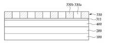
도 1을 참조하면, 본 발명의 일실시예에 따른 유기발광 표시장치는 기판(100), 표시부(200) 및 봉지층(300)을 포함한다.Referring to FIG. 1, an organic light emitting diode display according to an exemplary embodiment includes a
상기 기판(100)은 유리 기판, 석영 기판, 투명 수지 기판과 같은 다양한 재질로 형성될 수 있으며, 플렉서블한 재료를 이용하여 형성될 수도 있다. 상기 기판(100)으로 사용될 수 있는 투명 수지 기판은 폴리이미드 수지, 아크릴 수지, 폴리아크릴레이트 수지, 폴리카보네이트 수지, 폴리에테르 수지, 폴리에틸렌 테레프탈레이트 수지, 술폰산 수지 등을 포함할 수 있다.The
상기 유기 발광 표시 장치가 상기 기판(100)쪽으로 표시되는 배면 발광인 경우에는 상기 기판(100)은 광투과성 소재로 형성되어야 하지만, 상기 봉지층(300)으로 표시되는 전면 발광인 경우에는 상기 기판(100)은 반드시 광투과성 소재로 형성하지 않아도 무방하다.When the organic light emitting diode display is the bottom emission displayed toward the
상기 표시부(200)는 상기 발광층(220)을 포함하는 소자이다. 자세한 구성은 후술한다.The
상기 봉지층(300)은 유기막(320) 및 무기막(310)이 교대로 적층된 구조이다.The
도 2는 본 발명의 일실시예에 따른 패턴화 유기막을 포함하는 유기발광 표시장치를 나타낸 것이다.2 illustrates an organic light emitting display device including a patterned organic layer according to an embodiment of the present invention.
도 2를 참조하면, 본 발명의 일실시예에 따른 유기발광 표시장치는 기판(100), 상기 기판(100)상에 형성된 표시부(200) 및 상기 표시부(200)상에 형성된 봉지층(300)을 포함한다.2, an organic light emitting display device according to an exemplary embodiment of the present invention includes a
상기 봉지층(300)은 복수개의 무기막(310) 및 복수개의 유기막(320)을 포함하고, 상기 복수개의 무기막(310)과 상기 복수개의 유기막(320)은 교대로 적층되어 형성될 수 있다.The
상기 유기막(320)과 상기 무기막(310)의 적층 횟수는 외부 광 추출 효율 등을 고려하여 실시될 수 있다.The number of laminations of the
상기 유기발광 표시장치는 상기 표시부(200)와 다층구조를 가지는 상기 봉지층(300)을 포함하게 되고, 이러한 다층 구조 하에서는 유기발광 표시장치의 광학적 특성이 저하되는 문제점이 있었다.The organic light emitting display device may include the
즉 복수개의 무기막(310) 및 복수개의 유기막(320)을 포함하는 다층 구조에 있어서, 발광층(220)에서 발생한 빛의 일부가 내부 전반사로 구속되어 소멸되는 문제점이 있었다.That is, in the multilayer structure including the plurality of
이러한 광 추출 효율 저하를 막기 위해 본 발명에서는, 도 2에 도시된 바와 같이, 패턴화 유기막(330)을 포함할 수 있다. 상기 복수개의 유기막(320) 중 적어도 하나 이상을 선택하여 상기 패턴화 유기막(330)을 형성할 수 있다. 예를 들면, 제 1 무기막(311)을 형성하고, 상기 제 1 무기막(311)상에 상기 패턴화 유기막(330)을 형성하고, 상기 패턴화 유기막(330)상에 제 2 무기막(312)을 형성할 수 있다.In order to prevent such light extraction efficiency from being lowered in the present invention, as shown in FIG. 2, the patterned
상기 패턴화 유기막(330)은 유기물질로 된 매트릭스(330a)에 복수개의 고굴절률 부분(330b)이 산재하는 구조일 수 있다.The patterned
상기 복수개의 유기막(320)은 투습 방지와 평탄화 역할을 하므로 두께가 비교적 두껍게 형성된다. 상기 두꺼운 유기막(320)이 흘러내리는 걸 방지하기 위해, 유기물질(330')을 도포한 후에 자외선을 조사하여 상기 유기물질(330')을 경화 시킨다. 한편, 상기 자외선 조사량이 많을수록 유기물질(330')은 굴절률이 올라가는 성질이 있다. 따라서 본 발명의 상기 패턴화 유기막(330)은 경화과정 도중 자외선 조사량을 국부적으로 차이를 둠으로써 내부 영역의 굴절률이 서로 다르게 될 수 있다.Since the plurality of
예를 들면, 자외선 조사량이 적은 영역은 유기물질로 된 매트릭스(330a)가 되며, 자외선 조사량이 많은 영역은 고굴절률 부분(330b)이 될 수 있다.For example, a region having a small amount of ultraviolet radiation may be a
상기 유기물질로 된 매트릭스(330a)의 굴절률은 1.45 내지 1.5 일 수 있고, 상기 복수개의 고굴절률 부분(330b)의 굴절률은 1.5 내지 1.6 일 수 있다. 따라서 상기 유기물질로 된 매트릭스(330a)와 상기 복수개의 고굴절률 부분(330b)의 굴절률 차로 인하여 발광층(220)에서 발생된 빛을 산란 및 회절 시킬 수 있다.The refractive index of the
도 3은 본 발명의 일실시예에 따른 패턴화 유기막의 고굴절률 부분의 경계면에서 나타나는 광의 반사 및 굴절을 나타낸 도면이다. 도 3을 참조하면, 상기 복수개의 고굴절률 부분(330b)의 경계면에서 빛이 산란되거나 회절되는 것을 보여주고 있다.3 is a view showing reflection and refraction of light appearing at the interface of the high refractive index portion of the patterned organic film according to one embodiment of the present invention. Referring to FIG. 3, light is scattered or diffracted at the interface between the plurality of high
한편, 상기 유기물질로 된 매트릭스(330a)와 상기 고굴절률 부분(330b)는 동일 재료로 형성될 수 있다. 동일한 유기물질(330')을 도포한 후, 자외선 조사량의 차이에 따라 각 영역 별로 굴절률의 차이가 생기는 구조이므로, 상기 패턴화 유기막(330)은 동일 재료일 수 있고, 중합도 등에서 차이가 있을 수 있다.Meanwhile, the
도 4는 본 발명의 다른 실시예에 따른 패턴화 유기막을 포함하는 유기발광 표시장치를 나타낸 것이다. 도 4를 참조하면, 상기 패턴화 유기막(330)은 적어도 2개 층 이상 형성될 수 있다. 예를 들면, 상기 기판(100)상에 상기 표시부(200)가 형성되고, 상기 표시부(200)상에 캐핑층(400)이 형성될 수 있다. 상기 캐핑층(400)상에 제 1 무기막(311)을 형성하고, 제 1 무기막(311)상에 제 1 패턴화 유기막(331)을 형성하고, 상기 제 1 패턴화 유기막(331)상에 제 2 무기막(312)을 형성하고, 상기 제 2 무기막(312)상에 제 2 패턴화 유기막(332)를 형성할 수 있다. 그리고 제 3 무기막(313), 제 1 유기막(321), 제 4 무기막(314), 제 2 유기막(322) 및 제 5 무기막(315)을 순차로 적층할 수 있다.4 illustrates an organic light emitting display device including a patterned organic layer according to another exemplary embodiment of the present invention. Referring to FIG. 4, at least two layers of the patterned
상기 패턴화 유기막(330)을 2층 이상 형성함으로써, 광 추출 효율이 더 올라갈 수 있다.By forming two or more layers of the patterned
도 5는 본 발명의 일실시예에 따른 패턴화 유기막의 평면도이다. 도 5를 참조하면, 상기 패턴화 유기막(330)의 고굴절률 부분(330b)은 원기둥, 각기둥, 볼록렌즈 및 오목렌즈 중 어느 하나의 형태를 띌 수 있다.5 is a plan view of a patterned organic film according to an embodiment of the present invention. Referring to FIG. 5, the high
또한, 상기 패턴화 유기막(330)의 고굴절률 부분(330b)은 상기 유기물질로 된 매트릭스(330a)에 규칙적이거나 불규칙적으로 분포할 수 있다. 예를 들면, 제 1 패턴화 유기막(331)은 유기물질로 된 제 1 매트릭스(331a)에 제 1 고굴절률 부분(331b)이 원기둥 형태로 규칙적으로 분포할 수 있고, 제 2 패턴화 유기막(332)은 유기물질로 된 제 2 매트릭스(332a)에 제 2 고굴절률 부분(332b)이 원기둥 형태로 불규칙적으로 분포할 수 있다.In addition, the high
도 6은 본 발명의 또 다른 실시예에 따른 패턴화 유기막을 포함하는 유기발광 표시장치를 나타낸 것이다. 도 7은 본 발명의 또 다른 실시예에 따른 패턴화 유기막의 평면도이다. 도 6 및 도 7을 참조하면, 본 발명의 상기 패턴화 유기막(330) 2 개가 하나의 무기막(310)을 개재하여 적층되어 형성되며, 상기 2 개의 패턴화 유기막(330)의 고굴절률 부분(330b)은 라인 형태로 형성되며, 상기 2개의 패턴화 유기막(330) 중 상부 패턴화 유기막에 포함된 고굴절률 부분(330b)과 하부 패턴화 유기막에 포함된 고굴절률 부분(330b)이 서로 교차될 수 있다.6 illustrates an organic light emitting display device including a patterned organic layer according to another exemplary embodiment of the present invention. 7 is a plan view of a patterned organic film according to another embodiment of the present invention. 6 and 7, two patterned
예를 들면, 제 1 무기막(311)이 상기 캐핑층(400)상에 형성될 수 있고, 제 1 무기막(311)상에 제 3 패턴화 유기막(333)이 형성될 수 있다. 상기 제 3 패턴화 유기막(333)상에 제 2 무기막(312)이 형성될 수 있고, 상기 제 2 무기막(312)상에 제 4 패턴화 유기막(334)이 형성될 수 있다. 상기 제 4 패턴화 유기막(334)상에 제 3 무기막(313), 제 1 유기막(321), 제 4 무기막(314), 제 2 유기막(322) 및 제 5 무기막(315)이 순차적으로 적층될 수 있다.For example, a first
상기 제 3 패턴화 유기막(333)는 유기물질로 이루어진 제 3 매트릭스(333a)와 라인 형태의 제 3 고굴절률 부분(333b)로 이루어질 수 있고, 상기 제 4 패턴화 유기막(334)은 유기물질로 이루어진 제 4 매트릭스(334a)과 라인 형태의 제 4 고굴절률 부분(334b)으로 이루어질 수 있다.The third patterned
상기 고굴절률 부분(330b)은 상부에서 봤을 때, 슬릿과 같은 형태일 수 있다. 즉 상세하게는 상기 라인 형태는 소정의 높이와 두께를 가지는 긴 슬릿 일 수 있다. 따라서, 유기물질로 된 매트릭스(330a)와 고굴절률 부분(330b)이 길게 늘어진 슬릿 형태로 서로 반복될 수 있다.The high
상기 제 3 고굴절률 부분(333b)과 상기 제 4 고굴절률 부분(334b)은 상부에서 바라볼 때 서로 교차되게 형성될 수 있다. 도 7에서 보는 바와 같이, 제 3 고굴절률 부분(333b)은 제 1방향을 따라 형성될 수 있고, 제 4 고굴절률 부분(334b)은 제 1방향과 직교하는 제 2방향을 따라 형성될 수 있다. 따라서 제 3 고굴절률 부분(333b)와 제 4 고굴절률 부분(334b)은 서로 직교할 수 있고, 상기 발광층(220)에서 나오는 빛의 산란 및 회절을 증가시킬 수 있다. 상기 제 3 고굴절률 부분(333b)과 상기 제 4 고굴절률 부분(334b)이 교차되는 각도는 다양하게 형성될 수 있다.The third high
한편, 상기 무기막(310), 유기막(320) 및 패턴화 유기막(330)으로 사용 가능한 박막 재료 및 상기 무기막(310), 유기막(320) 및 패턴화 유기막(330)의 적층 방법은 이 분야에서 공지된 것이라면 특별히 제한 없이 사용할 수 있다.Meanwhile, a thin film material that can be used as the
상기 무기막(310)으로 사용 가능한 박막 재료로는 실리콘 질화물, 알루미늄 질화물, 지르코늄 질화물, 티타늄 질화물, 하프늄 질화물, 탄탈륨 질화물, 실리콘 산화물, 알루미늄 산화물 및 티타늄 산화물로 이루어진 군에서 적어도 하나를 포함하여 형성될 수 있다.The thin film material usable as the
상기 유기막(320)으로 사용 가능한 박막 재료로는 에폭시, 아크릴레이트, 우레탄아크릴레이트, 폴리우레아(Polyurea), 폴리아크릴레이트(Polyacrylate), PTCDA, BPDA 및 PMDA로 이루어진 군에서 적어도 하나를 포함하여 형성될 수 있다.The thin film material that can be used as the
상기 패턴화 유기막(330)은 자외선 경화성 수지로 사용가능한 유기막(320) 박막 재료를 사용하여 형성할 수 있다.The patterned
이외에도 이 분야에서 공지된 무기 박막 재료 또는 유기 박막 재료라면 본 발명의 무기막(310) 또는 유기막(320) 재료로 사용할 수 있다.In addition, any inorganic thin film material or organic thin film material known in the art may be used as the
상기 봉지층(300)을 구성하는 물질에 따라 상기 무기막(310) 및 유기막(320)은 스핀 코팅 공정, 프린팅 공정, 스퍼터링 공정, 화학 기상 증착 공정, 원자층 적층 공정, 플라즈마 증대 화학 기상 증착 공정, 고밀도 플라즈마-화학 기상 증착 공정, 진공 증착 공정 등을 이용하여 형성될 수 있다.The
한편, 상기 표시부(200)와 상기 봉지층(300) 사이에는 캐핑층(400)이 배치될 수 있고, 상기 캐핑층(400)은 자외선 흡수능이 있는 투명 재료로 형성될 수 있다.The
도 8은 도 2에 개시된 유기발광 표시장치를 더 상세히 표현한 도이다.FIG. 8 is a diagram illustrating in more detail the organic light emitting diode display illustrated in FIG. 2.
상기 표시부(200)는 상기 기판(100)상에 형성된 제 1 전극(210), 상기 제 1 전극(210) 사이에 형성되는 화소정의막(230)(Pixel Define Layer:PDL), 상기 제 1 전극(210) 상에 형성된 발광층(220) 및 상기 발광층(220) 상에 형성된 제 2 전극(240)을 포함할 수 있다.The
상기 유기발광 표시장치가 전면 발광인 경우, 상기 제 1 전극(210)은 금(Au), 백금(Pt), 니켈(Ni), 텅스텐(W), 크롬(Cr), 몰리브덴(Mo), 철(Fe), 코발트(Co), 구리(Cu), 팔라듐(Pd), 티탄(Ti) 및 이들의 화합물 중 적어도 하나를 포함하여 형성될 수 있으며, 상기 제 2 전극(240)은 투명 전도성 산화물인 산화인듐-산화주석(ITO:Indium Tin Oxide) 및 산화인듐-산화아연(IZO:Indium Zinc Oxide) 중 적어도 하나를 포함하여 형성될 수 있다.When the organic light emitting display is top emission, the
상기 유기발광 표시장치가 배면 발광인 경우, 상기 제 1 전극(210)은 높은 일함수를 갖는 투명 전도성 산화물인 산화인듐-산화주석(ITO:Indium Tin Oxide) 및 산화인듐-산화아연(IZO:Indium Zinc Oxide) 중 적어도 하나를 포함하여 형성될 수 있으며, 상기 제 2 전극(240)은 낮은 일함수를 갖는 금속 즉, 리튬(Li) 및 세슘(Cs)과 같은 알칼리 금속, 마그네슘(Mg), 칼슘(Ca) 및 스트론튬(Sr)과 같은 알칼리 토금속 및 이들의 화합물로 형성될 수 있다.When the organic light emitting display is a bottom emission, the
이외에도 상기 제 1 전극(210) 및 제 2 전극(240)은 당업계에 알려진 물질을 포함하여 형성될 수 있다.In addition, the
상기 발광층(220)은 적색 발광층, 녹색 발광층 및 청색 발광층을 포함할 수 있다. 상기 발광층(220)은 저분자 유기물 또는 고분자 유기물로 형성될 수 있다.The
상기 화소정의막(230)은 절연성을 갖는 재료로 형성되는데, 상기 제 1 전극(210)을 화소단위로 구분한다. 구체적으로, 상기 제 1 전극(210)의 모서리(edge)부에 상기 화소정의막(230)이 배치되어 상기 제 1 전극(210)을 화소단위로 구분함으로써 화소 영역을 정의한다. 상기 화소정의막(230)은 제 1 전극(210)의 가장자리를 덮는다.The
도 9a는 본 발명의 일실시예에 따른 슬릿 형태의 마스크를 나타낸 도면이다. 도 9b는 본 발명의 일실시예에 따른 사각 형태의 마스크를 나타낸 도면이다. 도 9c는 본 발명의 일실시예에 따른 규칙적인 분포를 가지는 원형 형태의 마스크를 나타낸 도면이다. 도 9d는 본 발명의 일실시예에 따른 불규칙적인 분포를 가지는 원형 형태의 마스크를 나타낸 도면이다. 도 10a 내지 도 10f는 본 발명의 일실시예에 따른 유기발광 표시장치의 제조과정을 나타낸 도면이다.9A is a view illustrating a slit-shaped mask according to an embodiment of the present invention. 9B illustrates a rectangular mask according to an embodiment of the present invention. 9C is a diagram illustrating a mask of a circular shape having a regular distribution according to an embodiment of the present invention. 9D illustrates a circular mask having an irregular distribution in accordance with an embodiment of the present invention. 10A through 10F illustrate a manufacturing process of an organic light emitting display device according to an exemplary embodiment of the present invention.
도 9a 내지 도 10f를 참조하면, 본 발명의 일례에서는 또한, 유기발광 표시장치의 제조방법을 제공한다.9A to 10F, an example of the present invention also provides a method of manufacturing an organic light emitting display device.
구체적으로 상기 제조방법은 기판(100)상에 표시부(200)를 형성하는 단계 및 상기 표시부(200)상에 봉지층(300)을 형성하는 단계를 포함할 수 있다.Specifically, the manufacturing method may include forming the
상기 봉지층(300)을 형성하는 단계는, 유기막(320)을 형성하는 단계와 무기막(310)을 형성하는 단계를 교대로 실시하며, 상기 유기막(320)을 형성하는 단계에서 적어도 하나의 유기막은, 유기막을 도포 후 선택적 광조사를 실시할 수 있다.The forming of the
상기 선택적 광조사를 실시하는 단계에서는, 하프톤(half tone) 마스크(500)를 이용할 수 있다. 상기 하프톤 마스크(500)는 광의 조사량을 조절할 수 있으며, 슬릿 형태의 마스크(501), 사각 형태의 마스크(502), 규칙적인 분포를 가지는 원형 형태의 마스크(503) 및 불규칙적인 분포를 가지는 원형 형태의 마스크(504)등이 있다. 상기 하프톤 마스크(500)는 슬릿 형태나 사각 및 원형 형태의 어두운 부분이 광을 보다 많이 통과시킬 수 있고, 밝은 나머지 부분은 광을 적게 통과시킬 수 있다. 상기 하프톤 마스크(500)의 종류로 예시된 4 개의 마스크는 예시적인 것에 불과하고, 당업자의 필요에 의해 변형된 하프톤 마스크로 발명을 실시할 수 있다.In the selective light irradiation step, a
상기 하프톤 마스크(500)는 패턴화될 유기물질(330') 위쪽에 배치되고, 상기 하프톤 마스크(500)상으로 광이 상기 유기물질(330')에 전면 조사될 수 있다.The
한편, 상기 선택적 광조사를 실시하는 단계에서는, 두개 이상의 광원에 의하여 광을 조사함으로써 상기 광의 간섭에 의하여 위치별 조사되는 광의 세기가 달라지게 함으로써 선택적 광조사가 이루어질 수 있다. 즉, 마스크 없이도, 상기 광의 간섭으로 인하여 상기 패턴화 유기막(330)을 형성할 수 있다.On the other hand, in the step of performing the selective light irradiation, the selective light irradiation may be made by varying the intensity of the light irradiated for each location by the interference of the light by irradiating light by two or more light sources. That is, even without a mask, the patterned
상기 광의 간섭을 이용한 광조사 방식은 홀로그램 리소그래피(hologram lithography) 방식의 한 종류일 수 있다. 상기 홀로그램 리소그래피는 다중빔 간섭에 의해 패턴을 형성하는 기법이다. 예를 들어 Two Beam Interference의 경우, 두 방향의 조사되는 빛이 중첩되어 보강을 일으켜 빛의 세기가 커지는 영역과 상쇄되어 빛의 세기가 0인 영역들이 주기적으로 만들어 질 수 있다. 이를 확장하여, Multi Beam Interference의 경우, 여러 빛이 서로 중첩하여 원형 또는 특정 모양을 형상화 할 수 있다.The light irradiation method using the interference of light may be one kind of hologram lithography method. Holographic lithography is a technique for forming a pattern by multibeam interference. In the case of Two Beam Interference, for example, two beams of irradiated light overlap each other to cause reinforcement, which is offset from a region in which the intensity of light increases, so that regions of zero light intensity may be periodically generated. By extending this, in the case of Multi Beam Interference, several lights may overlap each other to form a circular or specific shape.
한편, 상기 선택적 광조사를 실시하는 단계는 적어도 2 회 실시하며, 유기막 상부에 일방향의 슬릿 형태를 가진 마스크를 배치하여 상기 선택적 광조사를 실시하고, 그 다음 유기막 상부에 상기 일방향과 교차하는 다른 방향의 슬릿 형태를 가진 마스크를 배치하여 상기 선택적 광조사를 실시할 수 있다. 상세하게는, 먼저 유기막(320)을 도포한다. 상기 유기막(320) 위쪽에 일방향의 슬릿 형태를 가진 마스크를 배치한 후, 선택적 광조사를 실시한다. 상기 선택적 광조사로 인하여 형성된 패턴화 유기막(330) 상에 무기막(310)을 형성한 후, 다시 상기 무기막(310)상에 다음 유기막(320)을 도포한다. 그 후, 상기 다음 유기막(320) 위쪽에 상기 일방향과 교차하는 다른 방향의 슬릿 형태를 가진 마스크를 배치하여 선택적 광조사를 실시할 수 있다. 상기 과정을 통해, 도 7에서 도시된 바와 같이, 상기 제 3 패턴화 유기막(333)과 상기 제 4 패턴화 유기막(334)을 형성할 수 있다.The selective light irradiation may be performed at least twice, and the selective light irradiation may be performed by arranging a mask having a slit shape in one direction on the organic layer, and then crossing the one direction on the organic layer. The selective light irradiation may be performed by disposing a mask having a slit shape in a different direction. In detail, the
한편, 상기 패턴화 유기막(330)은 동일한 물질로 균일하게 도포될 수 있다.The patterned
도 10a 내지 도 10f를 참조하면, 상기 패턴화 유기막(330)을 포함하는 유기발광 표시장치의 제조방법의 일례는 다음과 같다. 우선 상기 기판(100)상에 상기 표시부(200)를 형성한 후, 상기 캐핑층(400)을 상기 표시부(200)상에 형성할 수 있다.(도 10a) 그 뒤, 상기 캐핑층(400)상에 제 1 무기막(311)을 형성할 수 있다.(도 10b) 상기 제 1 무기막(311)상에 유기물질(330')을 먼저 도포한다.(도 10c) 그리고 나서 하프톤 마스크(500)를 상기 유기물질(330') 위쪽에 배치하고 광을 조사할 수 있다.(도 10d) 그러고 나면, 제 1 무기막(311)상에 상기 패턴화 유기막(330)이 형성될 수 있다. 상기 패턴화 유기막(330)은 선택적 광조사로 인하여 유기물질로 된 매트릭스(330a) 및 복수개의 고굴절률 부분(330b)을 포함할 수 있다.(도 10e) 상기 패턴화 유기막(330)상에 제 2 무기막(312)을 형성할 수 있다.(도 10f)10A to 10F, an example of a method of manufacturing an organic light emitting display device including the patterned
이상에서 설명된 유기발광 표시장치 및 그의 제조방법의 실시예는 예시적인 것에 불과하며, 본 발명의 보호범위는 본 발명 기술분야의 통상의 지식을 가진 자라면 이로부터 다양한 변형 및 균등예를 포함할 수 있다.Embodiments of the organic light emitting display device and the manufacturing method thereof described above are merely exemplary, and the scope of protection of the present invention may include various modifications and equivalents from those skilled in the art. Can be.
100 : 기판
200 : 표시부210 : 제 1 전극
220 : 발광층230 : 화소정의막
240 : 제 2 전극
300 : 봉지층
310 : 무기막311 : 제 1 무기막
312 : 제 2 무기막313 : 제 3 무기막
314 : 제 4 무기막315 : 제 5 무기막
320 : 유기막321 : 제 1 유기막
322 : 제 2 유기막
330 : 패턴화 유기막
330' : 유기물질330a : 유기물질로 된 매트릭스
330b : 고굴절률 부분331 : 제 1 패턴화 유기막
331a : 제 1 매트릭스331b : 제 1 고굴절률 부분
332 : 제 2 패턴화 유기막332a : 제 2 매트릭스
332b : 제 2 고굴절률 부분333 : 제 3 패턴화 유기막
333a : 제 3 매트릭스333b : 제 3 고굴절률 부분
334 : 제 4 패턴화 유기막334a : 제 4 매트릭스
334b : 제 4 고굴절률 부분
400 : 캐핑층
500 : 하프톤 마스크
501 : 슬릿 형태의 마스크 502 : 사각 형태의 마스크
503 : 규칙적인 분포를 가지는 원형 형태의 마스크
504 : 불규칙적인 분포를 가지는 원형 형태의 마스크100: substrate
200: display portion 210: first electrode
220: light emitting layer 230: pixel defining layer
240: second electrode
300: encapsulation layer
310: inorganic film 311: first inorganic film
312: second inorganic film 313: third inorganic film
314: fourth inorganic film 315: fifth inorganic film
320: organic film 321: first organic film
322: second organic film
330 patterned organic film
330 ':
330b: high refractive index portion 331: first patterned organic film
331a:
332: second patterned
332b: second high refractive index portion 333: third patterned organic film
333a:
334: fourth patterned
334b: fourth high refractive index portion
400: capping layer
500: halftone mask
501: slit mask 502: square mask
503: circular mask with regular distribution
504: circular mask with irregular distribution
Claims (18)
Translated fromKorean상기 기판상에 배치되며, 발광층을 포함하는 표시부; 및
상기 표시부상에 배치된 봉지층;을 포함하며,
상기 봉지층은 적어도 하나의 무기막 및 적어도 하나의 유기막을 포함하고,
상기 적어도 하나의 무기막과 상기 적어도 하나의 유기막은 교대로 적층되어 배치되고,
상기 적어도 하나의 유기막은 제 1 유기막 패턴 및 평면상에서 상기 제 1 유기막 패턴을 둘러싸는 제 2 유기막 패턴을 포함하며,
상기 제 1 유기막 패턴의 굴절률은 상기 제 2 유기막 패턴의 굴절률보다 더 큰 유기발광 표시장치.Board;
A display unit disposed on the substrate and including a light emitting layer; And
And an encapsulation layer disposed on the display unit.
The encapsulation layer includes at least one inorganic film and at least one organic film,
The at least one inorganic film and the at least one organic film are alternately stacked,
The at least one organic film includes a first organic film pattern and a second organic film pattern surrounding the first organic film pattern on a plane.
The refractive index of the first organic layer pattern is greater than the refractive index of the second organic layer pattern.
상기 제 2 유기막 패턴의 굴절률은 1.45 내지 1.5 인 유기발광 표시장치.The method of claim 1,
An organic light emitting display device having a refractive index of the second organic layer pattern is 1.45 to 1.5.
상기 제 1 유기막 패턴의 굴절률은 1.5 내지 1.6 인 유기발광 표시장치.The method of claim 1,
An organic light emitting display device having a refractive index of 1.5 to 1.6.
상기 제 1 유기막 패턴은 원기둥, 각기둥, 볼록렌즈 및 오목렌즈 중 어느 하나의 형태를 갖는 유기발광 표시장치.The method of claim 1,
The organic light emitting display device may have any one of a cylinder, a prismatic pillar, a convex lens, and a concave lens.
상기 제 1 유기막 패턴과 상기 제 2 유기막 패턴은 동일 재료로 형성되는 유기발광 표시장치.The method of claim 1,
The organic light emitting display device of which the first organic layer pattern and the second organic layer pattern are formed of the same material.
상기 기판상에 배치되며, 발광층을 포함하는 표시부; 및
상기 표시부상에 배치된 봉지층;을 포함하며,
상기 봉지층은 적어도 하나의 무기막 및 적어도 하나의 유기막을 포함하고,
상기 적어도 하나의 무기막과 상기 적어도 하나의 유기막은 교대로 적층되어 배치되고,
상기 적어도 하나의 유기막은 적어도 하나의 무기막을 사이에 두고 배치된 제 1 유기막 및 제 2 유기막을 포함하며;
상기 제 1 유기막은, 제 1 방향을 따라 교변적으로 배치되며 서로 다른 굴절률을 갖는 제 1 유기막 패턴 및 제 2 유기막 패턴을 포함하며;
상기 제 2 유기막은, 상기 제 1 방향과 교차하는 제 2 방향을 따라 교변적으로 배치되며 서로 다른 굴절률을 갖는 제 3 유기막 패턴 및 제 4 유기막 패턴을 포함하는 유기발광 표시장치.Board;
A display unit disposed on the substrate and including a light emitting layer; And
And an encapsulation layer disposed on the display unit.
The encapsulation layer includes at least one inorganic film and at least one organic film,
The at least one inorganic film and the at least one organic film are alternately stacked,
The at least one organic film includes a first organic film and a second organic film disposed with at least one inorganic film interposed therebetween;
The first organic film includes a first organic film pattern and a second organic film pattern which are alternately arranged in a first direction and have different refractive indices;
The second organic layer may include a third organic layer pattern and a fourth organic layer pattern that are alternately arranged in a second direction crossing the first direction and have different refractive indices.
상기 표시부는,
상기 기판상에 배치된 제 1 전극;
상기 발광층 상에 배치된 제 2 전극;을 더 포함하며,
상기 발광층은 상기 제 1 전극 상에 배치된 유기발광 표시장치.The method of claim 1,
The display unit,
A first electrode disposed on the substrate;
A second electrode disposed on the light emitting layer;
The light emitting layer is disposed on the first electrode.
상기 표시부와 상기 봉지층 사이에 배치된 캐핑층을 더 포함하는 유기발광 표시장치.The method of claim 1,
An organic light emitting display device further comprising a capping layer disposed between the display unit and the encapsulation layer.
상기 표시부상에 봉지층을 형성하는 단계;를 포함하며,
상기 봉지층을 형성하는 단계는,
유기막을 형성하는 단계와 무기막을 형성하는 단계를 교대로 실시하며,
상기 유기막을 형성하는 단계에서 적어도 하나의 유기막을 형성할 때에는, 유기막을 도포 후 상기 유기막에 선택적 광조사를 실시하며,
상기 선택적 광조사를 실시하는 단계는,
두 개 이상의 광원들로 상기 유기막에 광을 조사하여 상기 광의 간섭에 의하여 상기 유기막의 위치별로 조사되는 광의 세기를 달라지게 함으로써 상기 유기막에 선택적으로 광조사가 이루어지도록 하는 유기발광 표시장치의 제조방법.Forming a display unit on the substrate; And
Forming an encapsulation layer on the display unit;
Forming the encapsulation layer,
Alternately forming an organic film and forming an inorganic film,
When forming at least one organic film in the step of forming the organic film, after applying the organic film is subjected to selective light irradiation on the organic film,
The performing of the selective light irradiation,
Fabrication of an organic light emitting display device in which light is irradiated to the organic layer selectively by irradiating light to the organic layer with two or more light sources to change the intensity of light irradiated for each position of the organic layer by interference of the light Way.
상기 선택적 광조사를 실시하는 단계에서는,
하프톤(half tone) 마스크를 이용하여 선택적 광조사를 실시하는 유기발광 표시장치의 제조방법.The method of claim 10,
In the step of performing the selective light irradiation,
A method of manufacturing an organic light emitting display device that performs selective light irradiation using a half tone mask.
상기 유기막을 형성하는 단계에서는, 상기 유기막이 동일한 물질로 균일하게 도포되는 유기발광 표시장치의 제조방법.The method of claim 10,
In the forming of the organic layer, the organic layer is uniformly coated with the same material.
상기 표시부상에 봉지층을 형성하는 단계;를 포함하며,
상기 봉지층을 형성하는 단계는,
유기막을 형성하는 단계와 무기막을 형성하는 단계를 교대로 실시하며,
상기 유기막을 형성하는 단계에서 적어도 하나의 유기막을 형성할 때에는, 유기막을 도포 후 상기 유기막에 선택적 광조사를 실시하며,
상기 선택적 광조사를 실시하는 단계는 적어도 2 회 실시하며,
유기막 상부에 일방향의 슬릿 형태를 가진 마스크를 배치하여 선택적 광조사를 실시하고,
그 다음 유기막 상부에 상기 일방향과 교차하는 다른 방향의 슬릿 형태를 가진 마스크를 배치하여 선택적 광조사를 실시하는 유기발광 표시장치의 제조방법.Forming a display unit on the substrate; And
Forming an encapsulation layer on the display unit;
Forming the encapsulation layer,
Alternately forming an organic film and forming an inorganic film,
When forming at least one organic film in the step of forming the organic film, after applying the organic film is subjected to selective light irradiation on the organic film,
The selective light irradiation may be performed at least twice.
Selective light irradiation is performed by placing a mask having a slit shape in one direction on the organic layer,
Next, a method of manufacturing an organic light emitting display device, in which a mask having a slit shape in another direction crossing the one direction is disposed on the organic layer to perform selective light irradiation.
상기 제 1 유기막 패턴의 굴절률은 상기 제 2 유기막 패턴의 굴절률보다 더 크며;
상기 제 3 유기막 패턴의 굴절률은 상기 제 4 유기막 패턴의 굴절률보다 더 크며;
상기 제 1 유기막 패턴의 굴절률은 상기 제 3 유기막 패턴의 굴절률과 동일하며;
상기 제 2 유기막 패턴의 굴절률은 상기 제 4 유기막 패턴의 굴절률과 동일한 유기발광 표시장치.The method of claim 7, wherein
The refractive index of the first organic film pattern is greater than the refractive index of the second organic film pattern;
The refractive index of the third organic film pattern is greater than the refractive index of the fourth organic film pattern;
The refractive index of the first organic film pattern is the same as the refractive index of the third organic film pattern;
The refractive index of the second organic layer pattern is the same as the refractive index of the fourth organic layer pattern.
상기 제 1 유기막 패턴 및 상기 제 2 유기막 패턴은 각각 상기 제 2 방향으로 연장된 라인 형상을 가지며;
상기 제 3 유기막 패턴 및 상기 제 4 유기막 패턴은 각각 상기 제 1 방향으로 연장된 라인 형상을 갖는 유기발광 표시장치.The method of claim 7, wherein
The first organic film pattern and the second organic film pattern each have a line shape extending in the second direction;
The third organic layer pattern and the fourth organic layer pattern each have a line shape extending in the first direction.
상기 제 1 유기막과 상기 제 2 유기막은 적어도 하나의 무기막을 사이에 두고 서로 마주보게 배치된 유기발광 표시장치.The method of claim 7, wherein
The first organic layer and the second organic layer are disposed to face each other with at least one inorganic layer therebetween.
상기 제 1 유기막 패턴은 복수로 구비되며, 복수의 제 1 유기막 패턴들은 상기 제 2 유기막 패턴에 의해 분리되게 배치된 유기발광 표시장치.The method of claim 1,
The first organic layer pattern is provided in plurality, and the plurality of first organic layer patterns are separated by the second organic layer pattern.
Priority Applications (3)
| Application Number | Priority Date | Filing Date | Title |
|---|---|---|---|
| KR1020130040926AKR102044923B1 (en) | 2013-04-15 | 2013-04-15 | Organic light emitting display device and manufacturing method thereof |
| US14/018,912US9065076B2 (en) | 2013-04-15 | 2013-09-05 | Organic light emitting display device and manufacturing method thereof |
| CN201310520115.9ACN104103776B (en) | 2013-04-15 | 2013-10-29 | Organic light-emitting display device and its manufacture method |
Applications Claiming Priority (1)
| Application Number | Priority Date | Filing Date | Title |
|---|---|---|---|
| KR1020130040926AKR102044923B1 (en) | 2013-04-15 | 2013-04-15 | Organic light emitting display device and manufacturing method thereof |
Publications (2)
| Publication Number | Publication Date |
|---|---|
| KR20140123731A KR20140123731A (en) | 2014-10-23 |
| KR102044923B1true KR102044923B1 (en) | 2019-11-15 |
Family
ID=51671745
Family Applications (1)
| Application Number | Title | Priority Date | Filing Date |
|---|---|---|---|
| KR1020130040926AActiveKR102044923B1 (en) | 2013-04-15 | 2013-04-15 | Organic light emitting display device and manufacturing method thereof |
Country Status (3)
| Country | Link |
|---|---|
| US (1) | US9065076B2 (en) |
| KR (1) | KR102044923B1 (en) |
| CN (1) | CN104103776B (en) |
Cited By (1)
| Publication number | Priority date | Publication date | Assignee | Title |
|---|---|---|---|---|
| US12193298B2 (en) | 2020-12-11 | 2025-01-07 | Lg Display Co., Ltd. | Organic light emitting display apparatus |
Families Citing this family (26)
| Publication number | Priority date | Publication date | Assignee | Title |
|---|---|---|---|---|
| CN104393196A (en)* | 2014-10-17 | 2015-03-04 | 上海工程技术大学 | Manufacturing method of high-resolution-ratio organic light-emitting diode display |
| CN104466019A (en)* | 2014-11-25 | 2015-03-25 | 上海交通大学 | Structure and method for improving light extraction efficiency |
| CN104409657B (en)* | 2014-12-01 | 2018-10-02 | 昆山国显光电有限公司 | A kind of encapsulation cover plate and its application in Organnic electroluminescent device |
| KR102417119B1 (en)* | 2015-02-11 | 2022-07-06 | 삼성디스플레이 주식회사 | Flexible display device |
| KR102273053B1 (en) | 2015-02-16 | 2021-07-06 | 삼성디스플레이 주식회사 | Display apparatus |
| CN104900812A (en) | 2015-04-23 | 2015-09-09 | 京东方科技集团股份有限公司 | Film packaging structure, manufacture method thereof and display device |
| KR20180005323A (en) | 2016-07-05 | 2018-01-16 | 삼성디스플레이 주식회사 | Organic light-emitting display apparatus |
| KR102719753B1 (en)* | 2016-07-06 | 2024-10-18 | 삼성디스플레이 주식회사 | Organic light emitting diode display |
| CN106024845B (en)* | 2016-08-01 | 2019-02-26 | 深圳市华星光电技术有限公司 | A kind of organic light emitting diode display and preparation method thereof |
| KR102518130B1 (en) | 2016-08-04 | 2023-04-06 | 삼성디스플레이 주식회사 | Organic light emitting diode display |
| CN110121538B (en) | 2016-12-29 | 2023-05-26 | 3M创新有限公司 | Curable high refractive index ink compositions and articles prepared from the ink compositions |
| KR102783331B1 (en) | 2017-02-02 | 2025-03-20 | 삼성디스플레이 주식회사 | Organic light emitting display device |
| KR102332959B1 (en) | 2017-06-07 | 2021-12-01 | 삼성디스플레이 주식회사 | Display device |
| TWI627777B (en)* | 2017-07-26 | 2018-06-21 | 財團法人工業技術研究院 | Optical compensation structure |
| KR102408471B1 (en)* | 2017-11-14 | 2022-06-10 | 엘지디스플레이 주식회사 | Electroluminescence display device |
| WO2019135539A1 (en)* | 2018-01-03 | 2019-07-11 | 주식회사 엘지화학 | Optical film |
| CN108565349A (en)* | 2018-01-31 | 2018-09-21 | 京东方科技集团股份有限公司 | A kind of light emitting diode, its production method and display device |
| CN108630732B (en)* | 2018-04-25 | 2020-07-28 | 深圳市华星光电技术有限公司 | OLED display panel and manufacturing method thereof |
| CN108615816B (en)* | 2018-04-26 | 2020-06-05 | 武汉华星光电半导体显示技术有限公司 | OLED display panel |
| KR102568784B1 (en)* | 2018-08-23 | 2023-08-22 | 삼성디스플레이 주식회사 | Display device and manufacturing method thereof |
| KR102818046B1 (en)* | 2018-11-19 | 2025-06-11 | 삼성디스플레이 주식회사 | Display device |
| CN110690363B (en)* | 2019-10-25 | 2021-07-23 | 武汉华星光电半导体显示技术有限公司 | OLED display device |
| CN110850622A (en)* | 2019-11-21 | 2020-02-28 | 京东方科技集团股份有限公司 | Display panel, preparation method thereof and display device |
| CN111864094B (en)* | 2020-07-22 | 2023-04-18 | 京东方科技集团股份有限公司 | Light-emitting device, preparation method and display device |
| CN113328052B (en)* | 2021-05-17 | 2024-02-13 | 武汉华星光电技术有限公司 | display panel |
| CN115019657A (en)* | 2022-06-23 | 2022-09-06 | 深圳市华星光电半导体显示技术有限公司 | Display panel, method for producing the same, and display device |
Family Cites Families (12)
| Publication number | Priority date | Publication date | Assignee | Title |
|---|---|---|---|---|
| US6624568B2 (en)* | 2001-03-28 | 2003-09-23 | Universal Display Corporation | Multilayer barrier region containing moisture- and oxygen-absorbing material for optoelectronic devices |
| KR100581850B1 (en) | 2002-02-27 | 2006-05-22 | 삼성에스디아이 주식회사 | Organic electroluminescent display and manufacturing method |
| JP4032918B2 (en)* | 2002-10-24 | 2008-01-16 | ソニー株式会社 | Display device and manufacturing method thereof |
| DE112005003229T5 (en)* | 2004-12-24 | 2008-03-06 | Cambridge Display Technology Ltd., Cambourne Business Park | Organic electroluminescent device |
| US9722209B2 (en)* | 2008-09-25 | 2017-08-01 | Lg Display, Co., Ltd. | Organic light-emitting diodes (OLEDS) with high efficiency and its manufacturing method |
| KR20110051587A (en)* | 2009-11-10 | 2011-05-18 | 삼성전자주식회사 | Optical plate and its manufacturing method |
| KR101255626B1 (en)* | 2009-11-20 | 2013-04-16 | 주식회사 엘지화학 | Optical sheet for light extracting and beam-shaping for organic light emitting diodes |
| KR101318374B1 (en)* | 2009-12-03 | 2013-10-16 | 한국전자통신연구원 | Organic light emitting diode and manufacturing method thereof |
| KR20120044675A (en)* | 2010-10-28 | 2012-05-08 | 한국전자통신연구원 | Organic light emitting devices having a light extracting layer and methods of fabricating the same |
| JP2012204103A (en) | 2011-03-24 | 2012-10-22 | Toshiba Corp | Organic electroluminescent element, display device and luminaire |
| KR20120115841A (en)* | 2011-04-11 | 2012-10-19 | 삼성디스플레이 주식회사 | Organic light emitting diode display |
| KR101873476B1 (en)* | 2011-04-11 | 2018-07-03 | 삼성디스플레이 주식회사 | Organic light emitting diode display and manufacturing method thereof |
- 2013
- 2013-04-15KRKR1020130040926Apatent/KR102044923B1/enactiveActive
- 2013-09-05USUS14/018,912patent/US9065076B2/enactiveActive
- 2013-10-29CNCN201310520115.9Apatent/CN104103776B/enactiveActive
Cited By (1)
| Publication number | Priority date | Publication date | Assignee | Title |
|---|---|---|---|---|
| US12193298B2 (en) | 2020-12-11 | 2025-01-07 | Lg Display Co., Ltd. | Organic light emitting display apparatus |
Also Published As
| Publication number | Publication date |
|---|---|
| CN104103776A (en) | 2014-10-15 |
| KR20140123731A (en) | 2014-10-23 |
| US20140306193A1 (en) | 2014-10-16 |
| CN104103776B (en) | 2017-11-24 |
| US9065076B2 (en) | 2015-06-23 |
Similar Documents
| Publication | Publication Date | Title |
|---|---|---|
| KR102044923B1 (en) | Organic light emitting display device and manufacturing method thereof | |
| KR102679028B1 (en) | Organic Light Emitting Diode Display Device | |
| KR102012046B1 (en) | Organic light emitting display device and manufacturing method thereof | |
| US8963414B2 (en) | Organic electroluminescent device, lighting apparatus, and method for manufacturing the organic electroluminescent device | |
| JP6191287B2 (en) | Display device | |
| KR102253870B1 (en) | Organic light emitting display device | |
| US8841656B2 (en) | Organic electroluminescent element, lighting apparatus, and method for manufacturing organic electroluminescent element | |
| US8902383B2 (en) | Organic electroluminescent device, lighting apparatus, and method for manufacturing the organic electroluminescent device | |
| US10811639B2 (en) | Display device and a method of manufacturing the same | |
| EP2986082A1 (en) | Light-emitting device | |
| JP2007080579A (en) | Surface light emitting device | |
| KR102405943B1 (en) | Color Filter Array Substrate and Method For Fabricating the Same, and Organic Light Emitting Diode Display Device Using the Same | |
| KR102245505B1 (en) | Dual display device and method for fabricating the same | |
| KR20130113642A (en) | Substrate for oled with enhanced light extraction efficiency, method for fabricating thereof and oled having the same | |
| KR20060027330A (en) | Optical device and organic EL display | |
| KR102673170B1 (en) | Organic light emitting diode display and method for fabricating the same | |
| US9634281B2 (en) | Organic light-emitting display apparatus and method of manufacturing the same | |
| WO2016080310A1 (en) | Organic electroluminescence device and method for manufacturing organic electroluminescence device | |
| KR20160029491A (en) | Organic light emitting display device and method of manufacturing the same | |
| KR20220007788A (en) | Display device and method of fabricating the same | |
| EP3307024B1 (en) | Organic el element | |
| US20150132875A1 (en) | Mask for forming layer, forming method of layer, and manufacturing method of organic light-emitting diode (oled) display using the same | |
| KR102608318B1 (en) | Organic Light Emitting Device | |
| JP2016136484A (en) | Surface light-emitting device | |
| JP6522311B2 (en) | Light emitting device |
Legal Events
| Date | Code | Title | Description |
|---|---|---|---|
| PA0109 | Patent application | Patent event code:PA01091R01D Comment text:Patent Application Patent event date:20130415 | |
| PG1501 | Laying open of application | ||
| A201 | Request for examination | ||
| PA0201 | Request for examination | Patent event code:PA02012R01D Patent event date:20180329 Comment text:Request for Examination of Application Patent event code:PA02011R01I Patent event date:20130415 Comment text:Patent Application | |
| E902 | Notification of reason for refusal | ||
| PE0902 | Notice of grounds for rejection | Comment text:Notification of reason for refusal Patent event date:20190225 Patent event code:PE09021S01D | |
| E701 | Decision to grant or registration of patent right | ||
| PE0701 | Decision of registration | Patent event code:PE07011S01D Comment text:Decision to Grant Registration Patent event date:20190824 | |
| PR0701 | Registration of establishment | Comment text:Registration of Establishment Patent event date:20191108 Patent event code:PR07011E01D | |
| PR1002 | Payment of registration fee | Payment date:20191111 End annual number:3 Start annual number:1 | |
| PG1601 | Publication of registration | ||
| PR1001 | Payment of annual fee | Payment date:20221025 Start annual number:4 End annual number:4 | |
| PR1001 | Payment of annual fee | Payment date:20231023 Start annual number:5 End annual number:5 | |
| PR1001 | Payment of annual fee | Payment date:20241022 Start annual number:6 End annual number:6 |