KR102039454B1 - Symmetric plasma process chamber - Google Patents
Symmetric plasma process chamberDownload PDFInfo
- Publication number
- KR102039454B1 KR102039454B1KR1020120114793AKR20120114793AKR102039454B1KR 102039454 B1KR102039454 B1KR 102039454B1KR 1020120114793 AKR1020120114793 AKR 1020120114793AKR 20120114793 AKR20120114793 AKR 20120114793AKR 102039454 B1KR102039454 B1KR 102039454B1
- Authority
- KR
- South Korea
- Prior art keywords
- region
- chamber body
- processing
- assembly
- disposed
- Prior art date
- Legal status (The legal status is an assumption and is not a legal conclusion. Google has not performed a legal analysis and makes no representation as to the accuracy of the status listed.)
- Active
Links
Images


Classifications
- H—ELECTRICITY
- H01—ELECTRIC ELEMENTS
- H01J—ELECTRIC DISCHARGE TUBES OR DISCHARGE LAMPS
- H01J37/00—Discharge tubes with provision for introducing objects or material to be exposed to the discharge, e.g. for the purpose of examination or processing thereof
- H01J37/32—Gas-filled discharge tubes
- H01J37/32009—Arrangements for generation of plasma specially adapted for examination or treatment of objects, e.g. plasma sources
- H01J37/32082—Radio frequency generated discharge
- H01J37/32091—Radio frequency generated discharge the radio frequency energy being capacitively coupled to the plasma
- H—ELECTRICITY
- H01—ELECTRIC ELEMENTS
- H01J—ELECTRIC DISCHARGE TUBES OR DISCHARGE LAMPS
- H01J37/00—Discharge tubes with provision for introducing objects or material to be exposed to the discharge, e.g. for the purpose of examination or processing thereof
- H01J37/32—Gas-filled discharge tubes
- H01J37/32009—Arrangements for generation of plasma specially adapted for examination or treatment of objects, e.g. plasma sources
- H01J37/32082—Radio frequency generated discharge
- H—ELECTRICITY
- H01—ELECTRIC ELEMENTS
- H01J—ELECTRIC DISCHARGE TUBES OR DISCHARGE LAMPS
- H01J37/00—Discharge tubes with provision for introducing objects or material to be exposed to the discharge, e.g. for the purpose of examination or processing thereof
- H01J37/32—Gas-filled discharge tubes
- H01J37/32431—Constructional details of the reactor
- H01J37/3244—Gas supply means
- H—ELECTRICITY
- H01—ELECTRIC ELEMENTS
- H01J—ELECTRIC DISCHARGE TUBES OR DISCHARGE LAMPS
- H01J37/00—Discharge tubes with provision for introducing objects or material to be exposed to the discharge, e.g. for the purpose of examination or processing thereof
- H01J37/32—Gas-filled discharge tubes
- H01J37/32431—Constructional details of the reactor
- H01J37/32458—Vessel
- H01J37/32477—Vessel characterised by the means for protecting vessels or internal parts, e.g. coatings
- H01J37/32495—Means for protecting the vessel against plasma
- H—ELECTRICITY
- H01—ELECTRIC ELEMENTS
- H01J—ELECTRIC DISCHARGE TUBES OR DISCHARGE LAMPS
- H01J37/00—Discharge tubes with provision for introducing objects or material to be exposed to the discharge, e.g. for the purpose of examination or processing thereof
- H01J37/32—Gas-filled discharge tubes
- H01J37/32431—Constructional details of the reactor
- H01J37/32532—Electrodes
- H01J37/32541—Shape
- H—ELECTRICITY
- H01—ELECTRIC ELEMENTS
- H01J—ELECTRIC DISCHARGE TUBES OR DISCHARGE LAMPS
- H01J37/00—Discharge tubes with provision for introducing objects or material to be exposed to the discharge, e.g. for the purpose of examination or processing thereof
- H01J37/32—Gas-filled discharge tubes
- H01J37/32431—Constructional details of the reactor
- H01J37/32532—Electrodes
- H01J37/32568—Relative arrangement or disposition of electrodes; moving means
- H—ELECTRICITY
- H01—ELECTRIC ELEMENTS
- H01J—ELECTRIC DISCHARGE TUBES OR DISCHARGE LAMPS
- H01J37/00—Discharge tubes with provision for introducing objects or material to be exposed to the discharge, e.g. for the purpose of examination or processing thereof
- H01J37/32—Gas-filled discharge tubes
- H01J37/32431—Constructional details of the reactor
- H01J37/32715—Workpiece holder
- H01J37/32724—Temperature
- H—ELECTRICITY
- H01—ELECTRIC ELEMENTS
- H01J—ELECTRIC DISCHARGE TUBES OR DISCHARGE LAMPS
- H01J37/00—Discharge tubes with provision for introducing objects or material to be exposed to the discharge, e.g. for the purpose of examination or processing thereof
- H01J37/32—Gas-filled discharge tubes
- H01J37/32431—Constructional details of the reactor
- H01J37/32733—Means for moving the material to be treated
- H01J37/32743—Means for moving the material to be treated for introducing the material into processing chamber
- H—ELECTRICITY
- H01—ELECTRIC ELEMENTS
- H01J—ELECTRIC DISCHARGE TUBES OR DISCHARGE LAMPS
- H01J37/00—Discharge tubes with provision for introducing objects or material to be exposed to the discharge, e.g. for the purpose of examination or processing thereof
- H01J37/32—Gas-filled discharge tubes
- H01J37/32431—Constructional details of the reactor
- H01J37/32798—Further details of plasma apparatus not provided for in groups H01J37/3244 - H01J37/32788; special provisions for cleaning or maintenance of the apparatus
- H01J37/32816—Pressure
- H01J37/32834—Exhausting
- H—ELECTRICITY
- H01—ELECTRIC ELEMENTS
- H01L—SEMICONDUCTOR DEVICES NOT COVERED BY CLASS H10
- H01L21/00—Processes or apparatus adapted for the manufacture or treatment of semiconductor or solid state devices or of parts thereof
- H01L21/67—Apparatus specially adapted for handling semiconductor or electric solid state devices during manufacture or treatment thereof; Apparatus specially adapted for handling wafers during manufacture or treatment of semiconductor or electric solid state devices or components ; Apparatus not specifically provided for elsewhere
- H01L21/683—Apparatus specially adapted for handling semiconductor or electric solid state devices during manufacture or treatment thereof; Apparatus specially adapted for handling wafers during manufacture or treatment of semiconductor or electric solid state devices or components ; Apparatus not specifically provided for elsewhere for supporting or gripping
- H01L21/687—Apparatus specially adapted for handling semiconductor or electric solid state devices during manufacture or treatment thereof; Apparatus specially adapted for handling wafers during manufacture or treatment of semiconductor or electric solid state devices or components ; Apparatus not specifically provided for elsewhere for supporting or gripping using mechanical means, e.g. chucks, clamps or pinches
- H01L21/68714—Apparatus specially adapted for handling semiconductor or electric solid state devices during manufacture or treatment thereof; Apparatus specially adapted for handling wafers during manufacture or treatment of semiconductor or electric solid state devices or components ; Apparatus not specifically provided for elsewhere for supporting or gripping using mechanical means, e.g. chucks, clamps or pinches the wafers being placed on a susceptor, stage or support
- H01L21/68742—Apparatus specially adapted for handling semiconductor or electric solid state devices during manufacture or treatment thereof; Apparatus specially adapted for handling wafers during manufacture or treatment of semiconductor or electric solid state devices or components ; Apparatus not specifically provided for elsewhere for supporting or gripping using mechanical means, e.g. chucks, clamps or pinches the wafers being placed on a susceptor, stage or support characterised by a lifting arrangement, e.g. lift pins
- H—ELECTRICITY
- H05—ELECTRIC TECHNIQUES NOT OTHERWISE PROVIDED FOR
- H05H—PLASMA TECHNIQUE; PRODUCTION OF ACCELERATED ELECTRICALLY-CHARGED PARTICLES OR OF NEUTRONS; PRODUCTION OR ACCELERATION OF NEUTRAL MOLECULAR OR ATOMIC BEAMS
- H05H1/00—Generating plasma; Handling plasma
- H05H1/24—Generating plasma
- H05H1/46—Generating plasma using applied electromagnetic fields, e.g. high frequency or microwave energy
- H—ELECTRICITY
- H01—ELECTRIC ELEMENTS
- H01J—ELECTRIC DISCHARGE TUBES OR DISCHARGE LAMPS
- H01J2237/00—Discharge tubes exposing object to beam, e.g. for analysis treatment, etching, imaging
- H01J2237/32—Processing objects by plasma generation
- H01J2237/33—Processing objects by plasma generation characterised by the type of processing
- H01J2237/332—Coating
- H01J2237/3321—CVD [Chemical Vapor Deposition]
- H—ELECTRICITY
- H01—ELECTRIC ELEMENTS
- H01J—ELECTRIC DISCHARGE TUBES OR DISCHARGE LAMPS
- H01J2237/00—Discharge tubes exposing object to beam, e.g. for analysis treatment, etching, imaging
- H01J2237/32—Processing objects by plasma generation
- H01J2237/33—Processing objects by plasma generation characterised by the type of processing
- H01J2237/332—Coating
- H01J2237/3322—Problems associated with coating
- H01J2237/3323—Problems associated with coating uniformity
- H—ELECTRICITY
- H01—ELECTRIC ELEMENTS
- H01J—ELECTRIC DISCHARGE TUBES OR DISCHARGE LAMPS
- H01J2237/00—Discharge tubes exposing object to beam, e.g. for analysis treatment, etching, imaging
- H01J2237/32—Processing objects by plasma generation
- H01J2237/33—Processing objects by plasma generation characterised by the type of processing
- H01J2237/334—Etching
- H01J2237/3343—Problems associated with etching
- H01J2237/3344—Problems associated with etching isotropy
Landscapes
- Physics & Mathematics (AREA)
- Engineering & Computer Science (AREA)
- Plasma & Fusion (AREA)
- Chemical & Material Sciences (AREA)
- Analytical Chemistry (AREA)
- Electromagnetism (AREA)
- Spectroscopy & Molecular Physics (AREA)
- General Physics & Mathematics (AREA)
- Condensed Matter Physics & Semiconductors (AREA)
- Manufacturing & Machinery (AREA)
- Computer Hardware Design (AREA)
- Microelectronics & Electronic Packaging (AREA)
- Power Engineering (AREA)
- Drying Of Semiconductors (AREA)
- Plasma Technology (AREA)
- Chemical Vapour Deposition (AREA)
- Container, Conveyance, Adherence, Positioning, Of Wafer (AREA)
Abstract
Translated fromKoreanDescription
Translated fromKorean본 발명은 일반적으로 전극들 사이에 인가되는 RF 파워에 의해 플라즈마가 생기는 기판 제조용 플라즈마 프로세싱 장치에 관한 것이다. 더 상세하게는, 본 발명은 개선된 플라즈마 균일성 제어를 위해 전기적, 가스 흐름, 및 열적 대칭성을 제공하는 플라즈마 프로세싱 챔버에 관한 것이다.BACKGROUND OF THE INVENTION Field of the Invention The present invention generally relates to a plasma processing apparatus for manufacturing a substrate in which plasma is generated by RF power applied between electrodes. More particularly, the present invention relates to a plasma processing chamber that provides electrical, gas flow, and thermal symmetry for improved plasma uniformity control.
평판 디스플레이(FPDs) 및 집적회로와 같은 전자 장치들은 통상 층들이 기판 상에 증착되고 증착된 재료가 원하는 패턴으로 식각되는 일련의 프로세스 단계들에 의해 제조된다. 상기 프로세스 단계들은 통상 물리 기상 증착(PVD), 화학 기상 증착(CVD), 플라즈마 강화 CVD(PECVD), 및 다른 플라즈마 프로세싱을 포함한다. 특히, 플라즈마 프로세스는 진공 챔버에 프로세싱 가스 혼합물을 공급하고, 전기 또는 전자기 파워(RF 파워)를 인가하여 상기 프로세스 가스를 플라즈마 상태로 여기 시킬 것을 요구한다. 상기 플라즈마는 상기 가스 혼합물을 원하는 증착 또는 식각 프로세스들을 수행하는 이온 종들로 분해한다.Electronic devices such as flat panel displays (FPDs) and integrated circuits are typically manufactured by a series of process steps in which layers are deposited on a substrate and the deposited material is etched in a desired pattern. The process steps typically include physical vapor deposition (PVD), chemical vapor deposition (CVD), plasma enhanced CVD (PECVD), and other plasma processing. In particular, the plasma process requires supplying a processing gas mixture to the vacuum chamber and applying electrical or electromagnetic power (RF power) to excite the process gas into a plasma state. The plasma decomposes the gas mixture into ionic species that perform the desired deposition or etching processes.
플라즈마 프로세스들에서 직면하는 하나의 문제는 프로세싱 동안 기판 표면 상부에 균일한 플라즈마 밀도를 수립하는 것에 관련된 어려움인데, 이는 기판의 중앙과 가장자리 영역들 사이의 불균일 프로세싱으로 이어진다. 균일한 플라즈마 밀도를 수립함에 있어서의 이 어려움에 대한 하나의 이유는 물리적인 프로세스 챔버 디자인에서의 비대칭성에 기인한 자연적인 전기적, 가스 흐름, 및 열적 왜곡(skews)을 수반한다. 이러한 왜곡은 물론 방위각의 불균일 플라즈마 밀도를 초래할 뿐만 아니라, 중앙-대-가장자리 플라즈마 균일성을 제어하기 위한 다른 프로세싱 변수들 또는 "노브(knobs)"를 사용하기 어렵게 만든다.One problem facing plasma processes is the difficulty associated with establishing a uniform plasma density over the substrate surface during processing, which leads to non-uniform processing between the center and edge regions of the substrate. One reason for this difficulty in establishing a uniform plasma density involves natural electrical, gas flow, and thermal skews due to asymmetry in the physical process chamber design. This distortion not only results in azimuth non-uniform plasma density, but also makes it difficult to use other processing variables or "knobs" for controlling center-to-edge plasma uniformity.
그러므로 개선된 플라즈마 균일성 제어를 위해 전기적, 가스 흐름, 및 열정 대칭성을 개선하는 플라즈마 프로세싱 장치에 대한 요구가 있다.Therefore, there is a need for a plasma processing apparatus that improves electrical, gas flow, and passion symmetry for improved plasma uniformity control.
본 발명의 일 실시예에 있어서, 프로세싱 영역을 둘러싸는 챔버 본체와 덮개 어셈블리를 포함하는 플라즈마 프로세싱 장치가 제공된다. 기판 지지 어셈블리가 상기 챔버 본체 내에 배치된다. 상기 챔버 본체 내의 진공 배기 영역을 정의하는 배기 어셈블리가 제공된다. 상기 챔버 본체는 상기 기판 지지 어셈블리의 중심축에 대해 대칭적으로 배치되어 상기 프로세싱 영역을 상기 진공 배기 영역과 유체적으로 연결하는 복수개의 통로들을 포함한다.상기 기판 지지 어셈블리는 상기 프로세싱 및 진공 배기 영역들로부터 유체적으로 밀봉된 중앙 영역에 배치된 지지 페데스탈(pedestal) 및 하부 전극을 포함한다. 복수개의 액세스 튜브들이 상기 중앙 영역에의 접속을 제공하기 위해 상기 챔버 본체를 통해 위치하며 상기 기판 지지 어셈블리의 중심축에 대해 대칭적으로 정렬된다.In one embodiment of the present invention, a plasma processing apparatus is provided that includes a chamber body and a lid assembly surrounding a processing region. A substrate support assembly is disposed within the chamber body. An exhaust assembly is provided that defines a vacuum exhaust region within the chamber body. The chamber body includes a plurality of passages disposed symmetrically about a central axis of the substrate support assembly to fluidly connect the processing region with the vacuum exhaust region. The substrate support assembly includes a support pedestal and a bottom electrode disposed in a central region fluidly sealed from the processing and vacuum exhaust regions. A plurality of access tubes are positioned through the chamber body to provide a connection to the central region and are symmetrically aligned with respect to the central axis of the substrate support assembly.
또 다른 실시예에 있어서, 플라즈마 프로세싱 장치는 프로세싱 영역을 둘러싸는 챔버 본체와 덮개 어셈블리를 포함한다. 기판 지지 어셈블리는 상기 챔버 본체 내에 배치된다. 상기 덮개 어셈블리는 프로세싱 가스를 상기 프로세싱 영역으로 분배시키도록 구성된 중앙 매니폴드(manifold)와 프로세싱 가스를 상기 프로세싱 영역으로 분배시키도록 구성된 하나 또는 그 이상의 외측 매니폴드들을 갖는 상부 전극을 포함한다. 상기 덮개 어셈블리는 또한 상기 기판 지지 어셈블리의 중심축에 대해 대칭적으로 정렬된 복수개의 가스 튜브들을 통해 상기 하나 또는 그 이상의 외측 매니폴드들에 결합된 링 매니폴드를 포함한다.In yet another embodiment, the plasma processing apparatus includes a chamber body and a lid assembly surrounding the processing region. A substrate support assembly is disposed within the chamber body. The lid assembly includes a top manifold configured to distribute processing gas to the processing region and an upper electrode having one or more outer manifolds configured to distribute processing gas to the processing region. The lid assembly also includes a ring manifold coupled to the one or more outer manifolds through a plurality of gas tubes symmetrically aligned with respect to the central axis of the substrate support assembly.
또 다른 실시예에 있어서, 플라즈마 프로세싱 장치는 프로세싱 영역을 둘러싸는 챔버 본체와 덮개 어셈블리를 포함한다. 기판 지지 어셈블리가 상기 챔버 본체 내에 배치된다. 상부 라이너(upper liner)가 상기 챔버 본체 내에 배치되어 상기 프로세싱 영역을 둘러싼다. 상기 상부 라이너는 복수개의 슬롯들(slots)을 구비하는 원통형 벽을 갖는데, 이 슬롯들은 벽을 통해 배치되고 상기 기판 지지 어셈블리의 중심축에 대해 대칭적으로 정렬된다. 백킹 라이너(backing liner)가 상기 원통형 벽에 결합되어 상기 복수개의 슬롯들 중 적어도 하나를 덮는다. 메쉬(mesh) 라이너가 상기 기판 지지 어셈블리 주위에 배치되고 상기 상부 라이너에 전기적으로 결합된다.In yet another embodiment, the plasma processing apparatus includes a chamber body and a lid assembly surrounding the processing region. A substrate support assembly is disposed within the chamber body. An upper liner is disposed in the chamber body and surrounds the processing region. The upper liner has a cylindrical wall having a plurality of slots, which slots are disposed through the wall and are symmetrically aligned with respect to the central axis of the substrate support assembly. A backing liner is coupled to the cylindrical wall to cover at least one of the plurality of slots. A mesh liner is disposed around the substrate support assembly and electrically coupled to the top liner.
위에서 언급된 본 발명의 특징들이 상세하게 이해될 수 있도록, 위에서 간략하게 요약된 본 발명에 대한 더 구체적인 설명이 실시예들을 참조하여 제시되며, 그 중 몇몇은 다음 도면들에 예시된다. 그러나 본 발명은 다른 동등하게 효과적인 실시예들에도 허용될 수 있기 때문에, 다음 도면들은 단지 본 발명의 전형적인 실시예들을 예시하며, 따라서 본 발명의 사상을 제한하는 것으로 간주되지 않아야 한다는 것에 유의해야 한다.
도 1은 본 발명의 일 실시예에 따른 플라즈마 프로세싱 장치의 개략적인 단면도이다.
도 2는 도 1의 상기 프로세싱 장치의 상부 전극의 개략적인 평면도이다.
도 3a는 챔버 본체의 상부 부분 내에 배치되어 도 1의 상기 프로세싱 장치의 프로세싱 영역을 둘러싸는 상부 라이너 어셈블리의 개략적인 사시도이다. 도 3b는 상기 챔버 본체와 상기 상부 라이너 어셈블리의 일부의 부분 단면도이다.
도 4는 도 1에 도시된 선 4-4를 따라 취해진 상기 프로세싱 장치의 개략도이다.
도 5는 도 1의 상기 프로세싱 장치를 통해 연장하는 액세스 튜브들의 레이아웃의 개략도이다.BRIEF DESCRIPTION OF THE DRAWINGS In order that the features of the invention mentioned above may be understood in detail, a more detailed description of the invention briefly summarized above is presented with reference to embodiments, some of which are illustrated in the following figures. However, it should be noted that the following figures merely illustrate exemplary embodiments of the present invention, as the present invention may be tolerated to other equally effective embodiments, and therefore should not be regarded as limiting the spirit of the present invention.
1 is a schematic cross-sectional view of a plasma processing apparatus according to an embodiment of the present invention.
FIG. 2 is a schematic plan view of the upper electrode of the processing apparatus of FIG. 1.
3A is a schematic perspective view of an upper liner assembly disposed within the upper portion of the chamber body and surrounding the processing region of the processing apparatus of FIG. 1. 3B is a partial cross-sectional view of a portion of the chamber body and the upper liner assembly.
4 is a schematic diagram of the processing apparatus taken along line 4-4 shown in FIG.
5 is a schematic diagram of a layout of access tubes extending through the processing apparatus of FIG. 1.
앞서 언급했듯이, 종래 플라즈마 시스템의 문제는 상기 챔버 내의 비대칭성에 기인하여 균일한 플라즈마 밀도를 제공함에 있어서의 어려움이다. 본 발명의 실시예들은 상기 챔버를 통해 극히 대칭적인 전기적, 열적 및 가스 흐름 전도성을 허용하는 챔버 디자인을 제공함으로써 이 문제를 경감한다. 이러한 대칭성을 제공함으로써, 상기 챔버 내에 형성되는 플라즈마는 자연적으로 상기 챔버의 프로세싱 영역 내에 배치된 기판의 표면에 걸쳐 개선된 균일성을 갖는다. 나아가, 가스 주입구와 처리되는 기판 사이뿐만 아니라 상부 및 하부 전극들 사이의 간극을 조작하는 능력을 제공하는 것과 같은 다른 챔버 부가 기능들이 종래 시스템과 비교하여 플라즈마 프로세싱 및 균일성을 더 잘 제어할 수 있는 더 넓은 프로세스 윈도우를 제공한다.As mentioned above, a problem with conventional plasma systems is the difficulty in providing a uniform plasma density due to the asymmetry in the chamber. Embodiments of the present invention alleviate this problem by providing a chamber design that allows extremely symmetrical electrical, thermal and gas flow conductivity through the chamber. By providing this symmetry, the plasma formed in the chamber naturally has improved uniformity over the surface of the substrate disposed in the processing region of the chamber. Furthermore, other chamber additions, such as providing the ability to manipulate the gap between the gas inlet and the substrate being processed as well as between the upper and lower electrodes, may provide better control of plasma processing and uniformity compared to conventional systems. Provides a wider process window.
도 1은 본 발명의 일 실시예에 따른 플라즈마 프로세싱 장치(100)의 개략적인 단면도이다. 상기 플라즈마 프로세싱 장치(100)는 플라즈마 식각 챔버, 플라즈마 강화 화학 기상 증착 챔버, 물리 기상 증착 챔버, 플라즈마 처리 챔버, 이온 주입 챔버, 또는 다른 적합한 진공 프로세싱 챔버일 수 있다. 도 1에 보이듯이, 상기 플라즈마 프로세싱 장치(100)는 일반적으로 챔버 덮개 어셈블리(110), 챔버 본체 어셈블리(140) 및 배기 어셈블리(190)를 포함하며, 이들은 일괄하여 프로세싱 영역(102) 및 배기 영역(104)을 둘러싼다. 실제로, 프로세싱 가스들이 상기 프로세싱 영역(102)으로 도입되고 RF 파워를 이용하여 플라즈마로 점화된다. 기판(105)은 기판 지지 어셈블리(160) 상에 위치하고, 식각, 화학 기상 증착, 물리 기상 증착, 이온 주입, 플라즈마 어닐링, 플라즈마 처리(treating), 제거(abatement), 또는 다른 플라즈마 프로세스들과 같은 플라즈마 프로세스를 상기 기판(105) 상에 수행하도록 상기 프로세싱 영역(102) 내에 생성된 플라즈마에 노출된다. 상기 배기 어셈블리(190)에 의해 상기 프로세싱 영역(102)에 진공이 유지되는데, 상기 배기 어셈블리는 사용된 프로세싱 가스들 및 상기 플라즈마 프로세스에서의 부산물들을 상기 진공 배기 영역(104)을 통해 제거한다.1 is a schematic cross-sectional view of a
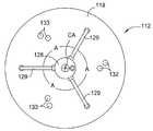
상기 덮개 어셈블리(110)는 상기 챔버 본체 어셈블리(140)로부터 절연되고 상기 챔버 본체 어셈블리에 의해 지지되는 상부 전극(112) 및 상기 상부 전극(112)을 둘러싸는 챔버 덮개(114)를 일반적으로 포함한다. 도 2는 상기 상부 전극(112)의 개략적인 평면도이다. 상기 상부 전극(112)은 전도성 가스 주입 튜브(126)를 통해 RF 파워 소스(103)에 결합된다. 상기 전도성 가스 주입 튜브(126)는 RF 파워 및 프로세싱 가스들 모두가 대칭적으로 제공되도록 상기 챔버 본체 어셈블리(140)의 중심축(CA)과 동축이다. 상기 상부 전극(112)은 열 전달 플레이트(118)에 부착된 샤워헤드 플레이트(116)를 포함한다. 상기 샤워헤드 플레이트(116), 열 전달 플레이트(118) 및 가스 주입 튜브(126)는 모두 알루미늄이나 스테인레스 스틸과 같은 RF 전도성 재료로 제조된다.The
상기 샤워헤드 플레이트(116)는 중앙 매니폴드(120)와 하나 또는 그 이상의 외측 매니폴드들(122)을 갖는다. 상기 하나 또는 그 이상의 외측 매니폴드들(122)은 상기 중앙 매니폴드(120)를 둘러싼다. 상기 중앙 매니폴드(120)는 상기 가스 주입 튜브(126)를 통해 가스 소스(106)로부터 프로세싱 가스들을 받고 복수개의 가스 통로들(121)을 통해 상기 프로세싱 영역(102)의 중앙부에 상기 수용된 프로세싱 가스들을 분배한다. 상기 외측 매니폴드(들)(122)은 상기 중앙 매니폴드(120)에 수용되는 가스들과 동일 또는 다른 혼합물일 수 있는 프로세싱 가스들을 상기 가스 소스(106)로부터 받는다. 상기 외측 매니폴드(들)(122)은 그 후 복수개의 가스 통로들(123)을 통해 상기 프로세싱 영역(102)의 외측 부분에 상기 수용된 프로세싱 가스들을 분배한다. 균일한 압력이 각 매니폴드(120, 122)와 연관된 각 가스 통로(121)에 제공되도록 상기 매니폴드들(120, 122)은 플레넘(plenum)으로 기능하기에 충분한 부피를 갖는다. 상기 샤워헤드 플레이트(116)의 상기 이중 매니폴드 구성은 상기 프로세싱 영역(102)으로의 가스들의 공급제어를 향상시킨다. 예를 들어, 상기 프로세싱 영역(102)의 상기 중앙부, 및 따라서 그 안에 위치하는 상기 기판(105)의 중앙부에 제공되는 프로세싱 가스들은 상기 프로세싱 영역(102)의 외측 부분, 및 따라서 상기 기판(105)의 외측 부분에 제공되는 상기 프로세싱 가스들과는 다른 유량(flow rate) 및/또는 압력으로 도입될 수 있다. 상기 다중 매니폴드 샤워헤드 플레이트(116)는 종래의 단일 매니폴드 버전들과 반대로 프로세싱 결과들의 중앙 대비 가장자리 제어를 강화할 수 있게 한다.The
도 1 및 도 2를 참조하면, 상기 가스 소스(106)로부터의 프로세싱 가스가 주입 튜브(127)를 통해 상기 주입 튜브(126) 둘레에 동심원으로 배치된 링 매니폴드(128) 내로 도입된다. 상기 링 매니폴드(128)로부터, 상기 프로세싱 가스는 복수개의 가스 튜브들(129)을 통해 상기 외측 매니폴드(들)(122)에 전달된다. 일 실시예에 있어서, 상기 링 매니폴드(128)는 가스가 동등하게 상기 링 매니폴드(128)로부터 상기 가스 튜브들(129)로 흐르는 것을 보증하는 회귀 가능한(recursive) 가스 경로를 포함한다. 상기 링 매니폴드(128) 및 상기 가스 튜브들(129)은 알루미늄 또는 스테인레스 스틸과 같은 전도성 재료로 제조된다. 따라서, 상기 링 매니폴드(128) 및 상기 가스 튜브들(129)은 상기 RF 전류의 대칭성에 영향을 미칠 수 있으며, 상기 상부 전극(112)에 의해 제공되는 전기장의 왜곡을 유발하고, 상기 프로세스 영역(102) 내의 플라즈마 균일성에 영향을 강하게 초래할 수 있다.1 and 2, processing gas from the
전기장에서의 이러한 왜곡을 방지하기 위해, 상기 가스 튜브들(129)은 상기프로세싱 장치(100)를 통해 수직하게 연장하는 중심축(CA) 주위에 대칭적으로 위치한다. 따라서, 상기 가스 튜브들(129)은 중앙에 위치하는 링 매니폴드(128)로부터 등각(A)으로 연장하여 상기 프로세싱 가스를 상기 냉각 플레이트(118)를 통해 그리고 상기 외측 매니폴드(들)(122) 내로 전달한다. 예를 들면, 도 2에 도시된 실시예는 120도 각도로 이격된 세 개의 가스 튜브들(129)을 나타낸다. 다른 예들(도시하지 않음)에 있어서, 상기 중심축(CA)에 대해 대칭적으로, 즉 서로 등각(A)으로 위치하는 한, 더 많거나 더 적은 가스 튜브들(129)이 사용될 수 있다. 링-형상의 매니폴드를 채용하고 상기 가스 튜브들(129)을 상기 중심축(CA)에 대해 대칭적으로 정렬함으로써, 상기 상부 전극(112)의 전기적 대칭성이 종래 시스템들에 비해 상당히 개선되어 상기 프로세싱 영역(102) 내에 더 균일하고 안정한(consistent) 플라즈마 형성을 가져온다. 추가로, 상기 가스 튜브들(129)의 대칭적인 정렬은 상기 외측 매니폴드(122) 내로 균일한 원형 배열(polar array)로 가스를 제공하고, 그것에 의해 상기 외측 매니폴드(122) 내에 방위각상의(azimuthal) 균일한 압력 분포, 및 그 결과로서, 상기 가스 통로들(123)을 통해 상기 프로세싱 영역(102)으로 가스의 방위각상 균일한 흐름을 제공하고, 그것에 의해 프로세싱 균일성을 향상시킨다.To prevent this distortion in the electric field, the
열 전달 유체가 유체 소스(109)로부터 유체 주입 튜브(130)를 통해 상기 열 전달 플레이트(118)로 전달된다. 상기 유체는 상기 열 전달 플레이트(118) 내에 배치된 하나 또는 그 이상의 유체 채널들(119)을 통해 순환되고 유체 배출 튜브(131)를 통해 상기 유체 소스(109)로 되돌아온다. 적합한 열 전달 유체들은 물, 물-기반 에틸렌 글리콜 혼합물, 과불소 폴리에테로(perfluoropolyether, 예컨대, Galden® 유체), 오일-기반 열 전달 유체들, 또는 유사한 유체들을 포함한다.Heat transfer fluid is transferred from the
상기 유체 주입 튜브(130) 및 유체 배출 튜브(131)는 적합한 플라스틱 재료와 같은 비전도성 재료로 제조된다. 따라서, 상기 튜브들 자체는 상기 상부 전극(112)의 전기적 대칭성에 영향을 주지 않는다. 그러나, 피팅들(fittings, 132)은 알루미늄이나 스테인레스 스틸과 같은 전도성 재료로 제조되고, 따라서 상기 상부 전극(112)의 전기적 대칭성에 영향을 미칠 수 있어 왜곡 효과를 유발할 수 있다. 따라서, 상기 피팅들(132)과 동일한 크기 및 형상을 갖고 동일한 재료로 제조되는, 전도성 플러그들(133)이 도 2에 도시된 바와 같이 중심축(CA)에 대해 대칭적으로 배치되어, 상기 플러그들(133) 및 피팅들(132)이 함께 상기 챔버 본체 어셈블리(140)의 중심축(CA)에 대해 중심축을 갖는 원형 배열을 정의한다. 상기 전도성 플러그들(133)의 추가는 상기 상부 전극(112)의 전기적 대칭성을 개선하여, 종래 시스템들에 적용가능한 것보다 상기 프로세싱 영역(102)에서 더 균일하고 안정한 플라즈마 형성을 가져온다.The
다시 도 1을 참조하면, 상기 챔버 본체 어셈블리(140)는 알루미늄 또는 스테인레스 스틸과 같은 프로세싱 환경들에 내성인 전도성 재료로 제조된 챔버 본체(142)를 포함한다. 상기 기판 지지 어셈블리(160)는 상기 챔버 본체(142) 내 중앙에 배치되고 상기 중심축(CA)에 대해 대칭적으로 상기 프로세싱 영역(102)에서 상기 기판(105)을 지지하도록 배치된다.Referring again to FIG. 1, the
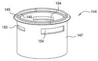
도 3a는 상기 챔버 본체(142)의 상부 부분 내에 배치되어 상기 프로세싱 영역(102)을 둘러싸는 상부 라이너 어셈블리(144)의 개략적인 사시도이다. 상기 상부 라이너 어셈블리(144)는 알루미늄, 스테인레스 스틸, 및/또는 이트리아(예를 들면, 이트리아 코팅된 알루미늄)와 같은 전도성의, 프로세스 호환성이 있는 재료로 구성될 수 있다. 실제로, 상기 상부 라이너 어셈블리(144)는 상기 프로세싱 영역(102) 내 플라즈마로부터 상기 챔버 본체(142)의 상부 부분을 차폐하며 주기적인 세정 및 유지 보수를 허용하도록 제거가능하다. 일 실시예에 있어서, 상기 상부 라이너 어셈블리(144)는 상기 챔버 내의 열적 대칭성 및 상기 프로세싱 영역(102) 내에 제공된 플라즈마의 대칭성을 강화하기 위해 예컨대 AC 히터(도시하지 않음)에 의해 온도 조절된다.3A is a schematic perspective view of an
도 1 및 3a를 참조하면, 상기 챔버 본체(142)는 상기 상부 라이너 어셈블리(144)의 외측 플랜지(145)를 지지하는 수평 돌기(ledge, 143)를 포함한다. 상기 상부 라이너 어셈블리(144)의 내측 플랜지(146)는 상기 상부 전극(112)을 지지한다. 절연체(113)가 상기 상부 라이너 어셈블리(144)와 상기 상부 전극(112) 사이에 위치하여 상기 챔버 본체 어셈블리(140)와 상기 상부 전극(112) 사이에 전기적 절연을 제공한다.1 and 3A, the
상기 상부 라이너 어셈블리(144)는 상기 내측 및 외측 플랜지들(146,145)에 부착된 외측 벽(147), 바닥 벽(148), 및 내측 벽(149)을 포함한다. 상기 외측 벽(147) 및 내측 벽(149)은 실질적으로 수직한 원통형 벽들이다. 상기 외측 벽(147)은 상기 프로세싱 영역(102) 내의 플라즈마로부터 챔버 본체(142)를 차폐하도록 위치하고, 상기 내측 벽(149)은 상기 프로세싱 영역(102) 내의 플라즈마로부터 상기 기판 지지 어셈블리(160)의 측면을 적어도 부분적으로 차폐하도록 위치한다. 상기 바닥 벽(148)은 본 명세서에서 후술하는 진공 배기 통로들(189)이 형성되는 특정 영역들을 제외하고 상기 내측 및 외측 벽들(149, 147)을 결합한다.The
다시 도 1을 참조하면, 상기 프로세싱 영역(102)은 상기 기판 지지 어셈블리(160)로/로부터 기판(105)의 진입 및 제거를 허용하는 상기 챔버 본체(142) 내에 배치된 슬릿 밸브 터널(141)을 통해 접근된다. 상기 상부 라이너 어셈블리(144)는 그것을 통해 배치된 슬롯(150)을 갖는데, 이 슬롯은 그것을 통한 상기 기판(105)의 통과를 허용하도록 상기 슬릿 밸브 터널(141)에 합치한다. 상기 챔버 본체 어셈블리(140)는, 상기 슬릿 밸브 터널(141)과 슬롯(150)을 밀봉하기 위해 상기 슬릿 밸브 도어(153)를 수직하게 뻗고 상기 슬릿 밸브 터널(141)과 슬롯(150)을 통해 접근을 허용하도록 상기 슬릿 밸브 도어(153)를 수직하게 오므리도록 구성되고 위치하는 액추에이터(152)를 포함하는 슬릿 밸브 도어 어셈블리(151)를 포함한다. 상기 슬릿 밸브 도어 어셈블리(151) 및 그 구성 부품들은 도면 혼잡을 최소화하기 위해 도 1에서 해칭되지 않는다. 상기 슬릿 밸브 도어(153)는 상기 라이너 내에 증가된 전기적 대칭성을 제공하기 위해 상기 상부 라이너 어셈블리(144)(예컨대, 이트리아 코팅된 알루미늄)와 실질적으로 합치하는 재료로 만들어질 수 있다. 일 실시예에 있어서, 상기 슬릿 밸브 도어(153)는 상기 상부 라이너 어셈블리(144)의 온도에 합치하여 상기 프로세싱 영역(102) 내에 증가된 열적 대칭성을 제공하도록 예컨대, AC 히터(도시하지 않음)에 의해 온도 조절된다.Referring again to FIG. 1, the
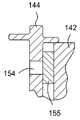
도 3a를 참조하면, 슬롯(150)의 크기 및 형상에 실질적으로 합치하는 추가적인 슬롯들(154)이 상기 상부 라이너 어셈블리(144)를 통해 배치된다. 상기 슬롯들(154)은 상기 중심축(CA)에 대해 대칭적으로 상기 상부 라이너 어셈블리(144)를 통해 배치된다. 예를 들면, 도 3a에 보이듯이, 두 개의 슬롯들(154)이 상기 슬롯(150)으로부터 120도의 각도로 배치되어, 상기 슬롯(150)과 슬롯들(154)이 상기 중심축(CA)에 대해 원형 배열(polar array)을 형성한다. 상기 슬롯들(154)은 상기 슬롯(150)의 존재에 기인하여 상기 상부 라이너 어셈블리(144) 내에 있는 전기적 전류 밀도 및/또는 분배에서의 변화를 보상하기 위해 상기 상부 라이너 어셈블리(144)에 대해 대칭적으로 배치된다. 덧붙여, 상기 슬롯들(150 및 154)은 각 가스 튜브들(129)과 나란하게 위치하여 상기 챔버 내에서 개선된 전기적 대칭성을 제공할 수 있다.Referring to FIG. 3A,
도 3b는 상기 챔버 본체(142)와 상기 상부 라이너 어셈블리(144)의 일부의 부분 단면도이다. 백킹 라이너들(155)이 제공되고, 상기 상부 라이너 어셈블리(144)의 슬롯들(154)에 부착되며 그것들을 덮을 수 있다. 상기 백킹 라이너들(155)은 상기 슬릿 밸브 도어(153)와 흡사하게 재료들로 만들어지고, 크기 및 형상이 정해진다. 상기 백킹 라이너들(backing liners, 155)은 또한 상기 상부 라이너 어셈블리(144)와 전도성 접촉하여 상기 상부 라이너 어셈블리(144)와 전기적 및 열적 접촉을 유지한다. 따라서, 상기 백킹 라이너들(155)은 종래 시스템들에 적용가능한 것보다 상기 프로세싱 영역(102) 내에 더 균일한 플라즈마 밀도를 가능하게 하기 위해 상기 상부 라이너 어셈블리(144)에 대해 전기적 뿐만 아니라 열적 대칭성을 더 제공한다.3B is a partial cross-sectional view of a portion of the
도 4는 도 1에 도시된 선 4-4를 따라 취해진 상기 프로세싱 장치(100)의 개략도이며, 상기 기판(105)은 명료하게 하기 위해 생략되었다. 도 1 및 도 4를 참조하면, 상기 기판 지지 어셈블리(160)는 상기 챔버 본체 어셈블리(140)의 중앙 영역(156) 내에서 중앙에 배치되고 상기 중심축(CA)을 공유한다. 즉, 중심축(CA)은 상기 기판 지지 어셈블리(160)의 중심을 수직으로 통과한다. 상기 기판 지지 어셈블리(160)는 일반적으로 상기 중심축(CA)이 그 중심을 통과하는 중공의 페데스탈(pedestal, 162) 및 하부 전극(161, 또는 캐소드)을 포함하며, 상기 중앙 영역(156)에 배치되고 상기 챔버 본체(142)에 의해 지지되는 중앙 지지 부재(157)에 의해 지지된다. 상기 중심축(CA)은 또한 상기 중앙 지지 부재(157)의 중심을 통과한다. 상기 하부 전극(161)은 뒤에 설명되듯이 상기 중공의 페데스탈(162)을 경유하는 케이블(도시하지 않음) 및 매칭 네트워크(도시하지 않음)를 통해 상기 RF 파워 소스(103)에 결합된다. RF 파워가 상기 상부 전극(112) 및 상기 하부 전극(161)에 공급될 때, 이들 사이에 형성되는 전기장이 상기 프로세싱 영역(102) 내에 있는 프로세싱 가스들을 플라즈마로 점화한다.4 is a schematic diagram of the
상기 중앙 지지 부재(157)는 예컨대, 패스너들fasteners) 및 오링들(o-rings)에 의해 상기 챔버 본체(142)에 밀봉되고, 상기 하부 전극(161)은 예컨대, 벨로우즈(bellows, 158)에 의해 상기 중앙 지지 부재(157)에 밀봉된다. 따라서, 상기 중앙 영역(156)은, 상기 프로세싱 영역(102)이 진공 조건으로 유지되는 동안, 상기 프로세싱 영역(102)으로부터 밀봉되어 대기압으로 유지될 수 있다.The
액추에이션 어셈블리(163)가 상기 중앙 영역(156) 내에 위치하고 상기 챔버 본체(142) 및/또는 상기 중앙 지지 부재(157)에 부착된다. 상기 액추에이션 어셈블리(163)는 도면 혼잡을 최소화하기 위해 해칭(hatching)없이 도시된 것에 유의하라. 상기 액추에이션 어셈블리(163)는 액추에이터(164, 예컨대, 모터), 리드 나사(lead screw, 165) 및 상기 페데스탈(162)에 부착된 너트(166)를 포함한다. 실제로, 상기 액추에이터(164)는 상기 리드 나사(165)를 회전시키고, 이것은 차례로 상기 너트(166), 및 따라서 상기 페데스탈(162)을 올리거나 내린다. 상기 하부 전극(161)이 상기 페데스탈(162)에 의해 지지되기 때문에, 상기 엑추에이션 어셈블리(163)는 상기 챔버 본체(142), 상기 중앙 지지 부재(157) 및 상기 상부 전극(112)에 대한 상기 하부 전극(161)의 수직 이동을 제공한다. 상기 프로세싱 영역(102) 내에서 상기 하부 전극(161)의 이러한 수직 이동은 상기 하부 전극(161)과 상기 상부 전극(112) 사이의 수직 간극을 제공하고, 이는 이들 사이에 형성되는 전기장의 제어를 향상시키고, 차례로, 상기 프로세싱 영역(102) 내에 형성되는 상기 플라즈마 내 밀도를 더 잘 제어하게 한다. 덧붙여, 상기 기판(105)이 상기 하부 전극(161)에 의해 지지되기 때문에, 상기 기판(105)과 상기 샤워헤드 플레이트(116) 사이의 간극이 또한 변할 수 있으며, 이는 상기 기판(105)에 걸쳐서 상기 프로세스 가스 분배를 더 잘 제어하게 한다.An
플라즈마 스크린(159)이 또한 제공되고, 상기 하부 전극(161)에 의해 지지되며 상기 상부 라이너 어셈블리(144)의 상기 내측 벽(149)과 중첩하여 상기 프로세싱 영역(102) 내 플라즈마로부터 상기 기판 지지 어셈블리(160) 및 상기 벨로우즈(158)을 보호한다. 상기 플라즈마 스크린(159)은 상기 페데스탈(162)에 결합하여 그것과 함께 수직으로 이동하므로, 상기 플라즈마 스크린(159)과 상기 상부 라이너 어셈블리(144)의 상기 내측 벽(149) 사이의 중첩은, 상기 플라즈마 스크린(159)과 상기 상부 라이너 어셈블리(144)가 이탈되지 않고 상기 페데스탈(162) 아래의 영역의 노출이 프로세스 가스들에 노출되는 것을 허용하지 않으면서 상기 페데스탈(162)이 이동 범위 전체를 이동하기에 충분하다.A
상기 기판 지지 어셈블리(160)는 상기 기판(105)의 로딩 및 언로딩을 촉진하기 위한 리프트 핀 어셈블리(167, lift pin assembly)를 더 포함한다. 상기 리프트 핀 어셈블리(167)는 리프트 핀 플레이트(169)에 부착된 리프트 핀들(168)을 포함한다. 상기 리프트 핀 플레이트(169)는 상기 하부 전극(161) 내 개구부(170) 내에 배치되고, 상기 리프트 핀들(168)은 상기 개구부(170)와 상기 프로세싱 영역(102) 사이에 배치된 리프트 핀 홀들(171)을 통해 내민다(extend). 상기 리프트 핀 플레이트(169)는 상기 하부 전극(161) 내 구멍(aperture, 173)을 통해 그리고 상기 중공의 페데스탈(162)로 내미는 리드 나사(172)에 결합된다. 액추에이터(195, 예컨대, 모터)는 상기 페데스탈(162) 상에 위치할 수 있다. 상기 액추에이터(195)는 도면 혼잡을 최소화하기 위해 해칭 없이 도시되었음에 유의하라. 상기 액추에이터(195)는 너트를 회전시키고, 이는 상기 리드 나사(172)를 나아가게 하거나 물러나게 한다. 상기 리드 나사(172)는 상기 리프트 핀 플레이트(169)에 결합된다. 따라서, 상기 액추에이터(195)는 상기 리드 나사(172)가 상기 리프트 핀 플레이트(169)를 들어올리거나 내려가게 하여, 상기 리프트 핀들(168)이 내밀거나 물러나게 한다. 그러므로 상기 액추에이터(195)는 상기 하부 전극(161)의 수직 위치에 무관하게 상기 리프트 핀들(168)을 내밀거나 물러나게 한다. 상기 리프트 핀들(168)의 이러한 독립적인 작동을 제공함으로써, 상기 기판(105)의 수직 위치가 상기 하부 전극(161)의 수직 위치로부터 독립적으로 변경될 수 있어, 예컨대, 후면 가스가 상기 기판 하부로부터 빠져나가는 것을 허용하는 프로세싱 동안 상기 기판을 들어올림으로써, 상기 기판(105)의 프로세싱 동안뿐만 아니라, 상기 기판(105)의 로딩 및 언로딩 동안에 위치 조절을 더 잘할 수 있게 한다.The
상기 기판 지지 어셈블리(160)는 상기 개구부(170)를 상기 배기 영역(104)과 결합하는 벤트 라인(vent line, 174)을 더 포함한다. 상기 벤트 라인(174)은 중앙으로 상기 중공의 페데스탈(162)을 거쳐, 그리고 뒤에서 설명되듯이 상기 중심축(CA)에 대해 대칭적인 스포크 패턴(spoke pattern)으로 정렬된 복수개의 액세스 튜브들(180) 중 하나를 거쳐 상기 챔버 본체(142) 밖으로 나간다. 상기 벤트 라인(174)은 상기 리프트 핀 홀들(171)을 통해 상기 개구부(170) 내로 샐 수 있는 프로세싱 가스들을 제거하기 위해 상기 개구부(170)의 진공 배기를 제공한다. 덧붙여, 상기 개구부(170)의 진공 배기는 또한 상기 하부 전극(161) 또는 리프트 핀들(168) 상에 배치된 상기 기판(105)의 뒷면에 존재할 수 있는 프로세싱 가스들을 제거하는데 도움이 된다.The
상기 기판 지지 어셈블리(160)는 또한 그것을 통해 배치되고 가스 서플라이 라인(178)을 통해 비활성 가스 서플라이(177)에 결합된 가스 포트(176)를 포함할 수 있다. 상기 가스 서플라이(177)는 프로세싱 가스들이 상기 기판(105)의 뒷면을 처리하는 것을 방지하기 위해 헬륨과 같은 비활성 가스를 상기 가스 서플라이 라인(178) 및 상기 가스 포트(176)를 통해 상기 기판(105)의 뒷면에 공급한다. 상기 가스 서플라이 라인(178)은 또한 상기 중공의 페데스탈(162)을 거쳐 상기 복수개의 액세스 튜브들(180) 중 하나를 통해 상기 챔버 본체(142)의 밖으로 나간다.The
상기 기판 지지 어셈블리(160)는 프로세싱 동안 상기 하부 전극(161)에 온도 제어를 제공하기 위해 열 교환 유체 소스(198)로부터 상기 하부 전극(161) 내의 하나 또는 그 이상의 열 교환 채널들(도시하지 않음)로 가는 하나 또는 그 이상의 유체 주입 라인들(179) 및 유체 배출 라인들(181)을 더 포함할 수 있다. 상기 유체 주입 라인들(179) 및 유체 배출 라인들(181)은 상기 하부 전극(161)으로부터 상기 중공의 페데스탈(162)을 거쳐 그리고 상기 복수개의 액세스 튜브들(180) 중 하나를 거쳐 상기 챔버 본체(142)의 밖으로 나간다.The
일 실시예에 있어서, 상기 기판 지지 어셈블리(160)는 상기 하부 전극(161)의 온도 제어를 쉽게 하기 위해 상기 하부 전극(161) 내에 배치된 하나 또는 그 이상의 온도 센서들(182)을 더 포함할 수 있다.In one embodiment, the
일 실시예에 있어서, 상기 하부 전극(161)은 정전기 척(chuck)이며, 따라서 내부에 배치된 하나 또는 그 이상의 전극들(도시하지 않음)을 포함한다. 전압 소스(도시하지 않음)가 상기 기판(105)에 대해 상기 하나 또는 그 이상의 전극들에 바이어스를 걸어 프로세싱 동안 상기 기판(105)을 제자리에 유지하기 위한 인력(attraction force)을 생성한다. 상기 전압 소스에 상기 하나 또는 그 이상의 전극들을 결합하는 케이블이 상기 중공의 페데스탈(162)을 거쳐 그리고 상기 복수개의 액세스 튜브들(180) 중 하나를 거쳐 상기 챔버 본체(142)의 밖으로 나간다.In one embodiment, the
도 5는 상기 챔버 본체 어셈블리(140)의 스포크들(191) 내 상기 액세스 튜브들(180)의 레이아웃의 개략도이다. 도 1 및 도 5를 참조하면, 상기 스포크들(191) 및 액세스 튜브들(180)은 도시된 바와 같은 스포크 패턴으로 상기 프로세싱 장치(100)의 중심축(CA)에 대해 대칭적으로 정렬된다. 도시된 실시예에 있어서, 세 개의 동일한 액세스 튜브들(180)이 상기 챔버 본체(142)를 통해 상기 중앙 영역(156) 내로 배치되어 상기 챔버 본체(142)의 외부로부터 상기 하부 전극(161)으로의 복수개의 튜브 가설(tubing) 및 케이블 가설(cabling)의 공급을 돕는다. 상기 하부 전극(162)의 수직 이동을 쉽게 하기 위해, 상기 액세스 튜브들(180) 각각을 통하는 개구부(183)는 상기 하부 전극(161)의 수직 행정과 대략 동일하다. 예를 들어, 일 구성예에서, 상기 하부 전극(162)은 약 7.2 인치의 거리를 수직 이동할 수 있다. 이 경우, 상기 액세스 튜브들(180) 각각 내의 상기 개구부(183)의 높이는 또한 약 7.2 인치이다. 이들 거리들을 대략 동일하게 유지하는 것이 상기 하부 전극(161)의 수직 이동 동안 상기 케이블 가설의 조임 및 마모를 방지할 뿐만 아니라 요구되는 케이블 가설의 길이를 최소화하게 한다. 덧붙여, 스포크들(191)의 폭(W)이 높은 종횡비(높이:폭)가 제공되도록 최소화되어, 유틸리티들(예컨대, 가스, 배선)을 위한 충분한 공간을 여전히 허용하면서 진공 배기 통로들(189)의 개방 면적이 보강된다. 이러한 구성은 배기 가스들의 흐름 저항을 감소시키고, 그 결과, 펌핑에 따른 에너지 소모를 감소시키고 더 적은 저렴한 비용의 펌프들이 사용될 수 있게 한다.5 is a schematic diagram of the layout of the
상기 하부 전극(161)으로의 케이블 여정(cable routing)을 더 쉽게 하기 위해, 상기 케이블 여정이 상기 복수개의 액세스 튜브들(180) 사이에서 분할된다. 예를 들어, 상기 유체 라인들(179, 181), 상기 가스 서플라이 라인(178) 및 상기 진공 튜브(174)는 모두 상기 액세스 튜브(180a)를 통해 제공될 수 있다; 상기 온도 센서들(184) 및 (예컨대, 액추에이터들(164, 195)로의) 다른 전기적 케이블들은 상기 액세스 튜브(180b)를 통해 제공될 수 있다; 그리고 상기 RF 전압 피드(feed) 및 (예컨대, 척킹 기능을 위한 전극들로의) 다른 전기적 케이블(들)은 상기 액세스 튜브(180c)를 통해 제공될 수 있다. 따라서, 상기 챔버 본체(142)의 외부로부터 상기 하부 전극(162)으로의 케이블 가설의 개수 및 부피는 상기 하부 전극(161)의 이동을 쉽게 하도록 적당한 여유를 제공하면서 상기 액세스 튜브들(180)의 크기를 최소화하기 위해 상기 액세스 튜브들(180) 사이에서 분할된다.To facilitate cable routing to the
상기 액세스 튜브들(180)은 알루미늄 또는 스테인레스 스틸과 같은 재료로 만들어질 수 있다. 상기 액세스 튜브들(180)의 대칭적인 스포크 정렬은 상기 프로세싱 장치(100)의 전기적 및 열적 대칭성을 더 촉진하도록 설계된다. 일 실시예에 있어서, 상기 액세스 튜브들(180)은 120도 떨어져 위치하고, 상기 액세스 튜브들(180) 각각은 각 가스 튜브(129)와 정렬된다. 프로세싱 동안 상기 프로세싱 영역(102) 내 훨씬 더 균일한 플라즈마 형성 및 상기 기판(105)의 표면에 걸쳐 플라즈마 밀도의 향상된 제어를 허용하기 위해, 상기 액세스 튜브들(180)의 대칭적인 정렬이 상기 챔버 본체(142) 내에 특히 상기 프로세싱 영역(102) 내에 전기적 및 열적 대칭성을 더 제공한다.The
다시 도 1 및 도 4를 참조하면, 상기 진공 배기 통로들(189)은 상기 중심축(CA)에 대해 대칭적으로 상기 상부 라이너 어셈블리(144) 내에 위치한다. 상기 진공 배기 통로들(189)은 상기 프로세싱 영역(102)으로부터 상기 진공 배기 영역(104)을 통해 그리고 상기 챔버 본체(142)의 밖으로 상기 배기 포트(196)를 통해 가스들의 진공 배기를 허용한다. 상기 가스들이 상기 진공 배기 통로들(189)을 통해 고르게 인출되도록 상기 배기 포트(196)는 상기 챔버 본체 어셈블리(140)의 중심축(CA)에 대해 중앙에 있다. 진공 배기 동안 프로세싱 가스들로부터 상기 챔버 본체(142)를 보호하기 위해 진공 배기 라이너들(187)이 상기 챔버 본체(142) 내에 제공된 진공 배기 채널들(188) 내에서 상기 진공 배기 통로들(189) 각각의 아래에 각각 위치할 수 있다. 상기 진공 배기 라이너들(187)은 위에서 설명된 바와 같이 상기 상부 라이너 어셈블리(144)와 유사한 재료들로 만들어질 수 있다.Referring again to FIGS. 1 and 4, the
상기 진공 배기 채널들(188)은 실질적으로 아무런 전기적 상호작용이 존재하지 않도록 상기 프로세싱 영역(102)으로부터 떨어져 위치한다. 그러나 상기 중심축(CA)에 대한 상기 진공 배기 채널들(188)의 대칭적인 위치 제어(positioning)는 상기 프로세싱 장치(100) 내에 개선된 열적 및 가스 흐름 대칭성을 제공한다. 예를 들어, 상기 중심축(CA)에 대한 상기 진공 배기 채널들(188)의 대칭적인 위치 제어, 및 따라서 상기 프로세싱 영역(102)은, 상기 프로세싱 영역(102)으로부터 가스들의 대칭적인 제거를 촉진하고, 그 결과, 상기 기판(105)을 가로질러 대칭적인 가스들의 흐름을 가져온다. 덧붙여, 상기 진공 배기 채널들(188)의 대칭적인 위치 제어, 및 따라서 상기 진공 배기 라이너들(187)은 상기 챔버 내 열적 분포에서의 대칭성을 진척시킨다. 따라서, 상기 프로세싱 장치(100) 내 상기 진공 배기 채널들(188)의 대칭적인 위치 제어는 상기 프로세싱 영역(102) 내에 균일한 플라즈마 형성을 촉진하고 상기 프로세싱 영역(102) 내 플라즈마 밀도 및 가스 흐름의 더 많은 제어를 허용한다.The
상기 배기 어셈블리(190)는 상기 챔버 본체(142)의 바닥에 상기 진공 배기 영역(104)에 인접하여 위치한다. 상기 배기 어셈블리는 진공 펌프(194)에 결합된 쓰로틀 밸브(192, throttle valve)를 포함할 수 있다. 상기 쓰로틀 밸브(192)는 상기 프로세싱 영역(102)으로부터 상기 진공 배기 통로들(189)을 통해 그리고 상기 챔버의 밖으로 상기 중앙에 위치하는 배기 포트(196)를 통해 배기 가스들을 대칭적으로 인출함으로써 상기 프로세싱 영역(102) 내 진공 조건들을 제어하기 위해 상기 진공 펌프(194)와 공동으로 사용되는 포핏 스타일 밸브(poppet style valve)일 수 있으며, 상기 프로세싱 영역(102) 내의 상기 플라즈마 조건들의 더 많은 제어를 더 제공할 수 있다. 포핏 스타일 밸브는, 도 1에 도시된 바와 같이, 균일한 360도 간극(198)을 제공하는데, 이 간극을 통해 진공 배기 가스들이 상기 배기 포트(196)를 통해 인출된다. 대조적으로, 종래의 댐퍼형 쓰로틀 밸브들은 진공 배기 가스들의 흐름에 대해 불균일한 간극을 제공한다. 예를 들어, 상기 댐퍼형 밸브가 열릴 때, 상기 밸브의 일측은 상기 밸브의 타측보다 더 많은 가스를 인출한다. 따라서, 상기 포핏 스타일 쓰로틀 밸브는 플라즈마 프로세싱 챔버들에 통상적으로 사용되는 전통적인 댐퍼형 쓰로틀 밸브보다 가스 전도성을 왜곡시키는 것에 더 적은 영향을 미친다.The
다시, 도 1 및 도 4를 참조하면, 전도성의, 경사진 메쉬 라이너(slant mesh liner, 400)가 상기 상부 라이너 어셈블리(144)의 하부 부분에 위치한다. 상기 경사진 메쉬 라이너(400)는 알루미늄, 스테인레스 스틸, 및/또는 이트리아(예컨대, 이트리아 코팅된 알루미늄)과 같은 전도성의 프로세스 호환성 재료로 만들어질 수 있다. 상기 경사진 메쉬 라이너(400)는 바닥 벽(402) 및 상기 바닥 벽(402)으로부터 바깥으로 그리고 상향 각도로 연장하는 외측 벽(404)을 가질 수 있다. 상기 외측 벽(404)은 그것을 통해 형성된 복수개의 구멍들(apertures, 410)을 가질 수 있다. 상기 구멍들(410)은 상기 경사진 메쉬 라이너(400)의 중심축에 대해 대칭적으로 위치하여 배기 가스들이 그것을 통해 균일하게 인출되도록 할 수 있으며, 이는 다시 상기 프로세싱 영역(102)에 균일한 플라즈마 형성을 돕고 상기 프로세싱 영역(102) 내의 플라즈마 밀도 및 가스 흐름의 더 많은 제어를 허용한다. 일 실시예에 있어서, 상기 경사진 메쉬 라이너(400)의 중심축은 상기 챔버 본체 어셈블리(140)의 중심축(CA)과 정렬된다.Referring again to FIGS. 1 and 4, a conductive,
상기 메쉬 라이너(400)의 바닥 벽(402)은 상기 상부 라이너 어셈블리(144)의 바닥 벽(148) 및/또는 내측 벽(149)에 전기적으로 결합될 수 있다. 추가로, 상기 메쉬 라이너(400)의 외측 벽(404)은 상기 상부 라이너 어셈블리(144)의 외측 벽(147)에 전기적으로 결합될 수 있다. RF 플라즈마가 상기 프로세싱 영역(102) 내에 있을 때, 접지로의 회귀 경로(return path)를 찾는 상기 RF 전류는 상기 메쉬 라이너(400)의 표면을 따라 상기 상부 라이너 어셈블리(144)의 외측 벽(147)으로 갈 수 있다. 따라서, 상기 메쉬 라이너(400)의 고리모양으로 대칭적인 구성은 접지로의 대칭적인 RF 회귀를 제공하며 상기 상부 라이너 어셈블리(400)의 하부 부분 내의 임의의 기하학적인 RF 비대칭성들을 우회한다.The
그러므로, 본 발명의 실시예들은 상기 챔버를 통해 극히 대칭적인 전기적, 열적 및 가스 흐름 전도를 허용하는 챔버 디자인을 제공함으로써 상기 챔버 내 비대칭성에 기인하여 균일한 플라즈마 밀도를 제공하기 어려운 종래의 플라즈마 시스템들의 문제를 해결한다. 이러한 대칭성을 제공함으로써, 상기 챔버 내에 형성되는 플라즈마는 자연적으로 상기 챔버의 프로세싱 영역 내에 배치된 기판의 표면을 가로질러 개선된 균일성을 갖는다. 이 개선된 대칭성뿐만 아니라, 가스 주입구와 처리되는 기판 사이뿐만 아니라 상부 및 하부 전극들 사이의 간극을 조작하는 능력을 제공하는 것과 같은 다른 챔버 부가 사항들은 종래 시스템들에 대비하여 플라즈마 프로세싱 및 균일성의 더 나은 제어를 허용한다.Therefore, embodiments of the present invention provide a chamber design that allows extremely symmetrical electrical, thermal and gas flow conduction through the chamber, making it difficult to provide uniform plasma density due to asymmetry in the chamber. Solve the problem. By providing this symmetry, the plasma formed in the chamber naturally has improved uniformity across the surface of the substrate disposed in the processing region of the chamber. In addition to this improved symmetry, other chamber additions such as providing the ability to manipulate the gap between the gas inlet and the substrate being processed as well as between the upper and lower electrodes further improve plasma processing and uniformity over conventional systems. Allows better control
앞에서 본 발명의 실시예들이 소개되지만, 본 발명의 다른 실시예들이 본 발명의 기본 사상을 벗어나지 않고 고안될 수 있으며, 본 발명의 사상은 다음의 청구범위에 의해 결정된다.While the embodiments of the present invention have been introduced above, other embodiments of the present invention can be devised without departing from the basic spirit thereof, and the spirit of the present invention is determined by the following claims.
100 프로세싱 장치 102 프로세싱 영역
103 rf 파워 소스 104 진공 배기 영역
105 기판 106 가스 소스
109 유체 소스 110 덮개 어셈블리
112 상부 전극 113 절연체
114 챔버 덮개 116 샤워헤드 플레이트
118 플레이트 119 유채 채널들
120 중앙 매니폴드 121 가스 통로
122 외측 매니폴드들 123 가스 통로들
126 가스 주입 튜브 127 주입 튜브
128 링 매니폴드 129 가스 튜브들
130 유체 주입 튜브 131 유체 배출 튜브
132 피팅들 133 전도성 플러그들
140 챔버 본체 어셈블리 141 슬릿 밸브 터널
142 챔버 본체 143 수평 돌기
144 상부 라이너 어셈블리 145 외측 플랜지
146 내측 플랜지 147 외측 벽
148 바닥 벽 149 내측 벽
150 슬롯들 151 슬릿 밸브 도어 어셈블리
152 액추에이터 153 슬릿 밸브 도어
154 슬롯들 155 백킹 라이너들
156 중앙 영역 157 중앙 지지 부재
158 벨로우즈 159 플라즈마 스크린
160 기판 지지 어셈블리 161 하부 전극
162 페데스탈 163 액추에이션 어셈블리
164 액추에이터들 165 리드 나사
166 너트 168 리프트 핀들
169 리프트 핀 플레이트 170 개구부
171 리프트 핀 홀들 172 리드 나사
173 구멍 174 진공 튜브
175 진공 소스 176 가스 포트
177 비활성 가스 서플라이 178 가스 서플라이 라인
179 유체 주입 라인들 180 액세스 튜브들
180a 액세스 튜브 180b 액세스 튜브
180c 액세스 튜브 181 유체 배출 라인들
183 개구부 184 온도 센서들
187 진공 배기 라이너들 188 진공 배기 채널들
190 배기 어셈블리 192 쓰로틀 밸브
194 진공 펌프 400 메쉬 라이너
402 바닥 벽 404 외측 벽
410 구멍들100
103
105
109
112
114
118
120
122
126
128
130
132
140
144
146
148
150
154
158
160
162
169
171 Lift Pin Holes 172 Lead Screw
173
175
177
179 Fluid Injection Lines 180 Access Tubes
183 openings 184 temperature sensors
187
190
194
402
410 holes
Claims (15)
Translated fromKorean프로세싱 영역을 둘러싸는 챔버 본체와 덮개 어셈블리; 및
상기 챔버 본체 내에 배치된 중심축을 갖는 기판 지지 어셈블리를 포함하되, 상기 기판 지지 어셈블리는,
상기 프로세싱 영역으로부터 유체적으로 밀봉된 상기 챔버 본체의 중앙 영역 내에 배치된 중공의 지지 페데스탈;
상기 중공의 지지 페데스탈에 의해 지지되는 하부 전극으로서, 상기 하부 전극은 내부에 개구부를 포함하는, 상기 하부 전극;
상기 중앙 영역 내에 배치되고 상기 하부 전극을 소정 거리 수직 이동시키도록 구성된 제1 액추에이션 장치;
상기 하부 전극 내의 상기 개구부 내에 배치된 복수개의 리프트 핀들로서, 하나 이상의 리프트 핀 홀들이 상기 하부 전극 내의 상기 개구부와 상기 프로세싱 영역 사이에 배치되는, 상기 복수개의 리프트 핀들; 및
상기 하부 전극 내의 상기 개구부를 상기 챔버 본체의 진공 배기 영역에 유체적으로 결합하는 진공 튜브로서, 상기 진공 튜브는 중앙으로 상기 중공의 지지 페데스탈을 통해 그리고 복수개의 액세스 튜브들 중 하나를 통해 상기 챔버 본체 밖으로 그리고 상기 진공 배기 영역으로 라우팅(route)되는, 상기 진공 튜브를 포함하며,
상기 중앙 영역은 상기 기판 지지 어셈블리의 중심축을 따라 상기 중앙 영역 아래에서 상기 챔버 본체 내에 배치된 진공 배기 영역으로부터 유체적으로 밀봉되고,
상기 챔버 본체와 함께 상기 진공 배기 영역을 정의하는 배기 어셈블리를 포함하되, 상기 챔버 본체는 상기 기판 지지 어셈블리의 중심축에 대해 대칭적으로 배치되어 상기 프로세싱 영역을 상기 진공 배기 영역과 유체적으로 연결하는 복수개의 통로들을 포함하고; 그리고
상기 중앙 영역에의 접속을 제공하기 위해 상기 챔버 본체를 통해 위치하며 상기 기판 지지 어셈블리의 중심축에 대해 대칭적으로 정렬된 상기 복수개의 액세스 튜브들을 포함하는 플라즈마 프로세싱 장치.In the plasma processing apparatus,
A chamber body and cover assembly surrounding the processing area; And
A substrate support assembly having a central axis disposed within the chamber body, wherein the substrate support assembly comprises:
A hollow support pedestal disposed in a central region of the chamber body fluidly sealed from the processing region;
A lower electrode supported by the hollow support pedestal, the lower electrode including an opening therein;
A first actuation device disposed in the central region and configured to move the lower electrode a predetermined distance vertically;
A plurality of lift pins disposed in the opening in the lower electrode, wherein one or more lift pin holes are disposed between the opening in the lower electrode and the processing region; And
A vacuum tube fluidly coupling the opening in the lower electrode to a vacuum exhaust region of the chamber body, the vacuum tube being centrally through the hollow support pedestal and through one of a plurality of access tubes The vacuum tube, routed out and to the vacuum exhaust zone,
The central region is fluidly sealed from a vacuum exhaust region disposed in the chamber body below the central region along a central axis of the substrate support assembly,
An exhaust assembly defining the vacuum exhaust region with the chamber body, wherein the chamber body is disposed symmetrically about a central axis of the substrate support assembly to fluidly connect the processing region with the vacuum exhaust region. A plurality of passages; And
And the plurality of access tubes positioned through the chamber body to provide a connection to the central region and symmetrically aligned with respect to a central axis of the substrate support assembly.
상기 리프트 핀 플레이트에 결합된 리드 나사; 및
상기 리드 나사를 진퇴시키도록 구성된 액추에이터를 포함하는 플라즈마 프로세싱 장치.The method according to claim 4, The second actuation device,
A lead screw coupled to the lift pin plate; And
And an actuator configured to retract the lead screw.
각각 전도성 피팅들을 갖는 하나 또는 그 이상의 유체 주입구 및 하나 또는 그 이상의 유체 배출구를 갖는 상부 전극; 및
복수개의 전도성 플러그들을 포함하되, 상기 전도성 피팅들 및 전도성 플러그들은 상기 기판 지지 어셈블리의 중심축에 대해 대칭적으로 정렬된 플라즈마 프로세싱 장치.The method of claim 1, wherein the cover assembly,
An upper electrode having one or more fluid inlets and one or more fluid outlets, each having conductive fittings; And
A plurality of conductive plugs, wherein the conductive fittings and the conductive plugs are symmetrically aligned with respect to the central axis of the substrate support assembly.
프로세싱 가스를 상기 프로세싱 영역으로 분배하도록 구성된 중앙 매니폴드 및 프로세싱 가스를 상기 프로세싱 영역으로 분배하도록 구성된 하나 또는 그 이상의 외측 매니폴드들을 갖는 상부 전극; 및
상기 기판 지지 어셈블리의 중심축에 대해 대칭적으로 정렬된 복수개의 가스 튜브들을 통해 상기 하나 또는 그 이상의 외측 매니폴드들에 결합된 링 매니폴드를 포함하는 플라즈마 프로세싱 장치.The method of claim 1, wherein the cover assembly,
An upper electrode having a central manifold configured to distribute processing gas to the processing region and one or more outer manifolds configured to distribute processing gas to the processing region; And
And a ring manifold coupled to the one or more outer manifolds through a plurality of gas tubes symmetrically aligned with respect to the central axis of the substrate support assembly.
Applications Claiming Priority (2)
| Application Number | Priority Date | Filing Date | Title |
|---|---|---|---|
| US201161543565P | 2011-10-05 | 2011-10-05 | |
| US61/543,565 | 2011-10-05 |
Related Parent Applications (1)
| Application Number | Title | Priority Date | Filing Date |
|---|---|---|---|
| KR1020120107823ADivisionKR101361757B1 (en) | 2011-10-05 | 2012-09-27 | Symmetric plasma process chamber |
Related Child Applications (1)
| Application Number | Title | Priority Date | Filing Date |
|---|---|---|---|
| KR1020190131891ADivisionKR102166643B1 (en) | 2011-10-05 | 2019-10-23 | Symmetric plasma process chamber |
Publications (2)
| Publication Number | Publication Date |
|---|---|
| KR20130037198A KR20130037198A (en) | 2013-04-15 |
| KR102039454B1true KR102039454B1 (en) | 2019-11-01 |
Family
ID=48022257
Family Applications (12)
| Application Number | Title | Priority Date | Filing Date |
|---|---|---|---|
| KR1020120107823AActiveKR101361757B1 (en) | 2011-10-05 | 2012-09-27 | Symmetric plasma process chamber |
| KR1020120114790AActiveKR102024584B1 (en) | 2011-10-05 | 2012-10-16 | Symmetric plasma process chamber |
| KR1020120114793AActiveKR102039454B1 (en) | 2011-10-05 | 2012-10-16 | Symmetric plasma process chamber |
| KR1020120114791AActiveKR101944895B1 (en) | 2011-10-05 | 2012-10-16 | Symmetric plasma process chamber |
| KR1020120114792AActiveKR102009783B1 (en) | 2011-10-05 | 2012-10-16 | Symmetric plasma process chamber |
| KR1020130043537AActiveKR102009784B1 (en) | 2011-10-05 | 2013-04-19 | Symmetric plasma process chamber |
| KR1020170107938AActiveKR101944894B1 (en) | 2011-10-05 | 2017-08-25 | Symmetric plasma process chamber |
| KR1020190131891AActiveKR102166643B1 (en) | 2011-10-05 | 2019-10-23 | Symmetric plasma process chamber |
| KR1020200130047AActiveKR102299994B1 (en) | 2011-10-05 | 2020-10-08 | Symmetric plasma process chamber |
| KR1020210102480AActiveKR102423749B1 (en) | 2011-10-05 | 2021-08-04 | Symmetric plasma process chamber |
| KR1020220084597AActiveKR102697479B1 (en) | 2011-10-05 | 2022-07-08 | Symmetric plasma process chamber |
| KR1020240108525APendingKR20240127935A (en) | 2011-10-05 | 2024-08-13 | Symmetric plasma process chamber |
Family Applications Before (2)
| Application Number | Title | Priority Date | Filing Date |
|---|---|---|---|
| KR1020120107823AActiveKR101361757B1 (en) | 2011-10-05 | 2012-09-27 | Symmetric plasma process chamber |
| KR1020120114790AActiveKR102024584B1 (en) | 2011-10-05 | 2012-10-16 | Symmetric plasma process chamber |
Family Applications After (9)
| Application Number | Title | Priority Date | Filing Date |
|---|---|---|---|
| KR1020120114791AActiveKR101944895B1 (en) | 2011-10-05 | 2012-10-16 | Symmetric plasma process chamber |
| KR1020120114792AActiveKR102009783B1 (en) | 2011-10-05 | 2012-10-16 | Symmetric plasma process chamber |
| KR1020130043537AActiveKR102009784B1 (en) | 2011-10-05 | 2013-04-19 | Symmetric plasma process chamber |
| KR1020170107938AActiveKR101944894B1 (en) | 2011-10-05 | 2017-08-25 | Symmetric plasma process chamber |
| KR1020190131891AActiveKR102166643B1 (en) | 2011-10-05 | 2019-10-23 | Symmetric plasma process chamber |
| KR1020200130047AActiveKR102299994B1 (en) | 2011-10-05 | 2020-10-08 | Symmetric plasma process chamber |
| KR1020210102480AActiveKR102423749B1 (en) | 2011-10-05 | 2021-08-04 | Symmetric plasma process chamber |
| KR1020220084597AActiveKR102697479B1 (en) | 2011-10-05 | 2022-07-08 | Symmetric plasma process chamber |
| KR1020240108525APendingKR20240127935A (en) | 2011-10-05 | 2024-08-13 | Symmetric plasma process chamber |
Country Status (5)
| Country | Link |
|---|---|
| US (8) | US9741546B2 (en) |
| JP (11) | JP6308716B2 (en) |
| KR (12) | KR101361757B1 (en) |
| CN (6) | CN103094045B (en) |
| TW (13) | TW201325326A (en) |
Families Citing this family (412)
| Publication number | Priority date | Publication date | Assignee | Title |
|---|---|---|---|---|
| US9394608B2 (en) | 2009-04-06 | 2016-07-19 | Asm America, Inc. | Semiconductor processing reactor and components thereof |
| US8802201B2 (en) | 2009-08-14 | 2014-08-12 | Asm America, Inc. | Systems and methods for thin-film deposition of metal oxides using excited nitrogen-oxygen species |
| TWI502617B (en)* | 2010-07-21 | 2015-10-01 | 應用材料股份有限公司 | Method,plasma processing apparatus ,and liner assembly for tuning electrical skews |
| KR20120043636A (en)* | 2010-10-26 | 2012-05-04 | 가부시키가이샤 한도오따이 에네루기 켄큐쇼 | Plasma treatment apparatus and plasma cvd apparatus |
| JP5837178B2 (en)* | 2011-03-22 | 2015-12-24 | アプライド マテリアルズ インコーポレイテッドApplied Materials,Incorporated | Liner assembly for chemical vapor deposition chambers |
| US20130023129A1 (en) | 2011-07-20 | 2013-01-24 | Asm America, Inc. | Pressure transmitter for a semiconductor processing environment |
| TW201325326A (en)* | 2011-10-05 | 2013-06-16 | Applied Materials Inc | Plasma processing equipment and substrate support assembly thereof |
| US9017481B1 (en) | 2011-10-28 | 2015-04-28 | Asm America, Inc. | Process feed management for semiconductor substrate processing |
| US10586686B2 (en)* | 2011-11-22 | 2020-03-10 | Law Research Corporation | Peripheral RF feed and symmetric RF return for symmetric RF delivery |
| WO2013078420A2 (en)* | 2011-11-24 | 2013-05-30 | Lam Research Corporation | Symmetric rf return path liner |
| US10170279B2 (en) | 2012-07-20 | 2019-01-01 | Applied Materials, Inc. | Multiple coil inductively coupled plasma source with offset frequencies and double-walled shielding |
| US9449794B2 (en) | 2012-07-20 | 2016-09-20 | Applied Materials, Inc. | Symmetrical inductively coupled plasma source with side RF feeds and spiral coil antenna |
| US9082590B2 (en) | 2012-07-20 | 2015-07-14 | Applied Materials, Inc. | Symmetrical inductively coupled plasma source with side RF feeds and RF distribution plates |
| US9879684B2 (en) | 2012-09-13 | 2018-01-30 | Kla-Tencor Corporation | Apparatus and method for shielding a controlled pressure environment |
| US10714315B2 (en) | 2012-10-12 | 2020-07-14 | Asm Ip Holdings B.V. | Semiconductor reaction chamber showerhead |
| US20160376700A1 (en) | 2013-02-01 | 2016-12-29 | Asm Ip Holding B.V. | System for treatment of deposition reactor |
| WO2014149200A1 (en) | 2013-03-15 | 2014-09-25 | Applied Materials, Inc. | Plasma reactor with highly symmetrical four-fold gas injection |
| KR102202406B1 (en)* | 2013-05-23 | 2021-01-13 | 어플라이드 머티어리얼스, 인코포레이티드 | A coated liner assembly for a semiconductor processing chamber |
| US9837250B2 (en)* | 2013-08-30 | 2017-12-05 | Applied Materials, Inc. | Hot wall reactor with cooled vacuum containment |
| KR101518398B1 (en)* | 2013-12-06 | 2015-05-08 | 참엔지니어링(주) | Substrate process apparatus |
| CN104752131B (en)* | 2013-12-25 | 2017-07-21 | 北京北方微电子基地设备工艺研究中心有限责任公司 | Top electrode assembly inlet duct and top electrode assembly |
| CN105408984B (en)* | 2014-02-06 | 2019-12-10 | 应用材料公司 | In-line decoupled plasma source chamber hardware design for enabling axial symmetry for improved flow conductance and uniformity |
| CN104862667B (en)* | 2014-02-26 | 2017-04-19 | 甘志银 | Symmetrical vapor deposition equipment reaction cavity |
| US11015245B2 (en) | 2014-03-19 | 2021-05-25 | Asm Ip Holding B.V. | Gas-phase reactor and system having exhaust plenum and components thereof |
| CN112366128B (en)* | 2014-04-09 | 2024-03-08 | 应用材料公司 | Flow modules for providing symmetrical flow paths in processing chambers |
| US20150371889A1 (en)* | 2014-06-20 | 2015-12-24 | Applied Materials, Inc. | Methods for shallow trench isolation formation in a silicon germanium layer |
| US10858737B2 (en) | 2014-07-28 | 2020-12-08 | Asm Ip Holding B.V. | Showerhead assembly and components thereof |
| KR102262109B1 (en)* | 2014-08-01 | 2021-06-10 | 세메스 주식회사 | Plasma generating device, apparatus for treating substrate comprising the same, and method for adjusting uniformity of substrate treatment |
| US9890456B2 (en) | 2014-08-21 | 2018-02-13 | Asm Ip Holding B.V. | Method and system for in situ formation of gas-phase compounds |
| JP6544902B2 (en)* | 2014-09-18 | 2019-07-17 | 東京エレクトロン株式会社 | Plasma processing system |
| US10941490B2 (en) | 2014-10-07 | 2021-03-09 | Asm Ip Holding B.V. | Multiple temperature range susceptor, assembly, reactor and system including the susceptor, and methods of using the same |
| JP6373160B2 (en)* | 2014-10-15 | 2018-08-15 | 東京エレクトロン株式会社 | Plasma processing equipment |
| KR102438139B1 (en) | 2014-12-22 | 2022-08-29 | 어플라이드 머티어리얼스, 인코포레이티드 | Process kit for a high throughput processing chamber |
| US11333246B2 (en)* | 2015-01-26 | 2022-05-17 | Applied Materials, Inc. | Chamber body design architecture for next generation advanced plasma technology |
| US10276355B2 (en) | 2015-03-12 | 2019-04-30 | Asm Ip Holding B.V. | Multi-zone reactor, system including the reactor, and method of using the same |
| US10049862B2 (en)* | 2015-04-17 | 2018-08-14 | Lam Research Corporation | Chamber with vertical support stem for symmetric conductance and RF delivery |
| KR101682155B1 (en)* | 2015-04-20 | 2016-12-02 | 주식회사 유진테크 | Substrate processing apparatus |
| KR101792941B1 (en)* | 2015-04-30 | 2017-11-02 | 어드밴스드 마이크로 패브리케이션 이큅먼트 인코퍼레이티드, 상하이 | A Chemical Vapor Deposition Apparatus and Its Cleaning Method |
| US10458018B2 (en) | 2015-06-26 | 2019-10-29 | Asm Ip Holding B.V. | Structures including metal carbide material, devices including the structures, and methods of forming same |
| US11004661B2 (en)* | 2015-09-04 | 2021-05-11 | Applied Materials, Inc. | Process chamber for cyclic and selective material removal and etching |
| US10211308B2 (en) | 2015-10-21 | 2019-02-19 | Asm Ip Holding B.V. | NbMC layers |
| US11139308B2 (en) | 2015-12-29 | 2021-10-05 | Asm Ip Holding B.V. | Atomic layer deposition of III-V compounds to form V-NAND devices |
| JP6607795B2 (en)* | 2016-01-25 | 2019-11-20 | 東京エレクトロン株式会社 | Substrate processing equipment |
| US10529554B2 (en) | 2016-02-19 | 2020-01-07 | Asm Ip Holding B.V. | Method for forming silicon nitride film selectively on sidewalls or flat surfaces of trenches |
| US10343920B2 (en) | 2016-03-18 | 2019-07-09 | Asm Ip Holding B.V. | Aligned carbon nanotubes |
| WO2017165016A1 (en)* | 2016-03-25 | 2017-09-28 | Applied Materials, Inc. | Chamber liner for high temperature processing |
| US10865475B2 (en) | 2016-04-21 | 2020-12-15 | Asm Ip Holding B.V. | Deposition of metal borides and silicides |
| US10190213B2 (en) | 2016-04-21 | 2019-01-29 | Asm Ip Holding B.V. | Deposition of metal borides |
| US10367080B2 (en) | 2016-05-02 | 2019-07-30 | Asm Ip Holding B.V. | Method of forming a germanium oxynitride film |
| US11453943B2 (en) | 2016-05-25 | 2022-09-27 | Asm Ip Holding B.V. | Method for forming carbon-containing silicon/metal oxide or nitride film by ALD using silicon precursor and hydrocarbon precursor |
| WO2017218044A1 (en)* | 2016-06-15 | 2017-12-21 | Applied Materials, Inc. | Gas distribution plate assembly for high power plasma etch processes |
| US11145495B2 (en) | 2016-06-15 | 2021-10-12 | Evatec Ag | Vacuum treatment chamber and method of manufacturing a vacuum treated plate-shaped substrate |
| KR101680850B1 (en)* | 2016-06-28 | 2016-11-29 | 주식회사 기가레인 | Plasma processing apparatus having control of exhaust flow path size |
| US9958782B2 (en)* | 2016-06-29 | 2018-05-01 | Applied Materials, Inc. | Apparatus for post exposure bake |
| US20180005851A1 (en)* | 2016-07-01 | 2018-01-04 | Lam Research Corporation | Chamber filler kit for dielectric etch chamber |
| US10612137B2 (en) | 2016-07-08 | 2020-04-07 | Asm Ip Holdings B.V. | Organic reactants for atomic layer deposition |
| US9859151B1 (en) | 2016-07-08 | 2018-01-02 | Asm Ip Holding B.V. | Selective film deposition method to form air gaps |
| KR102532607B1 (en) | 2016-07-28 | 2023-05-15 | 에이에스엠 아이피 홀딩 비.브이. | Substrate processing apparatus and method of operating the same |
| US9812320B1 (en) | 2016-07-28 | 2017-11-07 | Asm Ip Holding B.V. | Method and apparatus for filling a gap |
| US9887082B1 (en) | 2016-07-28 | 2018-02-06 | Asm Ip Holding B.V. | Method and apparatus for filling a gap |
| JP6738485B2 (en)* | 2016-08-26 | 2020-08-12 | アプライド マテリアルズ インコーポレイテッドApplied Materials,Incorporated | Low pressure lift pin cavity hardware |
| JP6994502B2 (en)* | 2016-08-26 | 2022-01-14 | アプライド マテリアルズ インコーポレイテッド | Plasma screen for plasma processing chamber |
| US10643826B2 (en) | 2016-10-26 | 2020-05-05 | Asm Ip Holdings B.V. | Methods for thermally calibrating reaction chambers |
| US11532757B2 (en) | 2016-10-27 | 2022-12-20 | Asm Ip Holding B.V. | Deposition of charge trapping layers |
| US10714350B2 (en) | 2016-11-01 | 2020-07-14 | ASM IP Holdings, B.V. | Methods for forming a transition metal niobium nitride film on a substrate by atomic layer deposition and related semiconductor device structures |
| US10229833B2 (en) | 2016-11-01 | 2019-03-12 | Asm Ip Holding B.V. | Methods for forming a transition metal nitride film on a substrate by atomic layer deposition and related semiconductor device structures |
| KR102546317B1 (en) | 2016-11-15 | 2023-06-21 | 에이에스엠 아이피 홀딩 비.브이. | Gas supply unit and substrate processing apparatus including the same |
| KR102762543B1 (en) | 2016-12-14 | 2025-02-05 | 에이에스엠 아이피 홀딩 비.브이. | Substrate processing apparatus |
| US11447861B2 (en) | 2016-12-15 | 2022-09-20 | Asm Ip Holding B.V. | Sequential infiltration synthesis apparatus and a method of forming a patterned structure |
| US11581186B2 (en) | 2016-12-15 | 2023-02-14 | Asm Ip Holding B.V. | Sequential infiltration synthesis apparatus |
| KR102700194B1 (en) | 2016-12-19 | 2024-08-28 | 에이에스엠 아이피 홀딩 비.브이. | Substrate processing apparatus |
| KR102587615B1 (en)* | 2016-12-21 | 2023-10-11 | 삼성전자주식회사 | Temperature controller of a plasma-processing apparatus and plasma-processing apparatus including the same |
| US10269558B2 (en) | 2016-12-22 | 2019-04-23 | Asm Ip Holding B.V. | Method of forming a structure on a substrate |
| US10867788B2 (en) | 2016-12-28 | 2020-12-15 | Asm Ip Holding B.V. | Method of forming a structure on a substrate |
| CN108257840B (en)* | 2016-12-29 | 2021-03-30 | 中微半导体设备(上海)股份有限公司 | Plasma processing device |
| CN106783500A (en)* | 2017-01-03 | 2017-05-31 | 京东方科技集团股份有限公司 | Filming equipment |
| US11390950B2 (en) | 2017-01-10 | 2022-07-19 | Asm Ip Holding B.V. | Reactor system and method to reduce residue buildup during a film deposition process |
| US10559451B2 (en)* | 2017-02-15 | 2020-02-11 | Applied Materials, Inc. | Apparatus with concentric pumping for multiple pressure regimes |
| US10468261B2 (en) | 2017-02-15 | 2019-11-05 | Asm Ip Holding B.V. | Methods for forming a metallic film on a substrate by cyclical deposition and related semiconductor device structures |
| US10529563B2 (en) | 2017-03-29 | 2020-01-07 | Asm Ip Holdings B.V. | Method for forming doped metal oxide films on a substrate by cyclical deposition and related semiconductor device structures |
| KR102457289B1 (en) | 2017-04-25 | 2022-10-21 | 에이에스엠 아이피 홀딩 비.브이. | Method for depositing a thin film and manufacturing a semiconductor device |
| US10770286B2 (en) | 2017-05-08 | 2020-09-08 | Asm Ip Holdings B.V. | Methods for selectively forming a silicon nitride film on a substrate and related semiconductor device structures |
| US10892156B2 (en) | 2017-05-08 | 2021-01-12 | Asm Ip Holding B.V. | Methods for forming a silicon nitride film on a substrate and related semiconductor device structures |
| US10886123B2 (en) | 2017-06-02 | 2021-01-05 | Asm Ip Holding B.V. | Methods for forming low temperature semiconductor layers and related semiconductor device structures |
| US12040200B2 (en) | 2017-06-20 | 2024-07-16 | Asm Ip Holding B.V. | Semiconductor processing apparatus and methods for calibrating a semiconductor processing apparatus |
| US11306395B2 (en) | 2017-06-28 | 2022-04-19 | Asm Ip Holding B.V. | Methods for depositing a transition metal nitride film on a substrate by atomic layer deposition and related deposition apparatus |
| KR20190009245A (en) | 2017-07-18 | 2019-01-28 | 에이에스엠 아이피 홀딩 비.브이. | Methods for forming a semiconductor device structure and related semiconductor device structures |
| US11018002B2 (en) | 2017-07-19 | 2021-05-25 | Asm Ip Holding B.V. | Method for selectively depositing a Group IV semiconductor and related semiconductor device structures |
| US11374112B2 (en) | 2017-07-19 | 2022-06-28 | Asm Ip Holding B.V. | Method for depositing a group IV semiconductor and related semiconductor device structures |
| US10541333B2 (en) | 2017-07-19 | 2020-01-21 | Asm Ip Holding B.V. | Method for depositing a group IV semiconductor and related semiconductor device structures |
| US10590535B2 (en) | 2017-07-26 | 2020-03-17 | Asm Ip Holdings B.V. | Chemical treatment, deposition and/or infiltration apparatus and method for using the same |
| TWI815813B (en) | 2017-08-04 | 2023-09-21 | 荷蘭商Asm智慧財產控股公司 | Showerhead assembly for distributing a gas within a reaction chamber |
| US10770336B2 (en) | 2017-08-08 | 2020-09-08 | Asm Ip Holding B.V. | Substrate lift mechanism and reactor including same |
| US10692741B2 (en) | 2017-08-08 | 2020-06-23 | Asm Ip Holdings B.V. | Radiation shield |
| US11769682B2 (en) | 2017-08-09 | 2023-09-26 | Asm Ip Holding B.V. | Storage apparatus for storing cassettes for substrates and processing apparatus equipped therewith |
| US11139191B2 (en) | 2017-08-09 | 2021-10-05 | Asm Ip Holding B.V. | Storage apparatus for storing cassettes for substrates and processing apparatus equipped therewith |
| US11830730B2 (en) | 2017-08-29 | 2023-11-28 | Asm Ip Holding B.V. | Layer forming method and apparatus |
| US11056344B2 (en) | 2017-08-30 | 2021-07-06 | Asm Ip Holding B.V. | Layer forming method |
| KR102491945B1 (en) | 2017-08-30 | 2023-01-26 | 에이에스엠 아이피 홀딩 비.브이. | Substrate processing apparatus |
| US11295980B2 (en) | 2017-08-30 | 2022-04-05 | Asm Ip Holding B.V. | Methods for depositing a molybdenum metal film over a dielectric surface of a substrate by a cyclical deposition process and related semiconductor device structures |
| KR102401446B1 (en) | 2017-08-31 | 2022-05-24 | 에이에스엠 아이피 홀딩 비.브이. | Substrate processing apparatus |
| US10510575B2 (en) | 2017-09-20 | 2019-12-17 | Applied Materials, Inc. | Substrate support with multiple embedded electrodes |
| KR102630301B1 (en) | 2017-09-21 | 2024-01-29 | 에이에스엠 아이피 홀딩 비.브이. | Method of sequential infiltration synthesis treatment of infiltrateable material and structures and devices formed using same |
| US10844484B2 (en) | 2017-09-22 | 2020-11-24 | Asm Ip Holding B.V. | Apparatus for dispensing a vapor phase reactant to a reaction chamber and related methods |
| US10658205B2 (en) | 2017-09-28 | 2020-05-19 | Asm Ip Holdings B.V. | Chemical dispensing apparatus and methods for dispensing a chemical to a reaction chamber |
| US10403504B2 (en) | 2017-10-05 | 2019-09-03 | Asm Ip Holding B.V. | Method for selectively depositing a metallic film on a substrate |
| US10636629B2 (en) | 2017-10-05 | 2020-04-28 | Applied Materials, Inc. | Split slit liner door |
| KR102470206B1 (en)* | 2017-10-13 | 2022-11-23 | 삼성디스플레이 주식회사 | Manufacturing method for metal oxide and display device comprising the metal oxide |
| US10923344B2 (en) | 2017-10-30 | 2021-02-16 | Asm Ip Holding B.V. | Methods for forming a semiconductor structure and related semiconductor structures |
| US10910262B2 (en) | 2017-11-16 | 2021-02-02 | Asm Ip Holding B.V. | Method of selectively depositing a capping layer structure on a semiconductor device structure |
| US11022879B2 (en) | 2017-11-24 | 2021-06-01 | Asm Ip Holding B.V. | Method of forming an enhanced unexposed photoresist layer |
| CN111344522B (en) | 2017-11-27 | 2022-04-12 | 阿斯莫Ip控股公司 | Including clean mini-environment device |
| WO2019103613A1 (en) | 2017-11-27 | 2019-05-31 | Asm Ip Holding B.V. | A storage device for storing wafer cassettes for use with a batch furnace |
| US10872771B2 (en) | 2018-01-16 | 2020-12-22 | Asm Ip Holding B. V. | Method for depositing a material film on a substrate within a reaction chamber by a cyclical deposition process and related device structures |
| KR102695659B1 (en) | 2018-01-19 | 2024-08-14 | 에이에스엠 아이피 홀딩 비.브이. | Method for depositing a gap filling layer by plasma assisted deposition |
| TWI799494B (en) | 2018-01-19 | 2023-04-21 | 荷蘭商Asm 智慧財產控股公司 | Deposition method |
| US11018047B2 (en) | 2018-01-25 | 2021-05-25 | Asm Ip Holding B.V. | Hybrid lift pin |
| USD880437S1 (en) | 2018-02-01 | 2020-04-07 | Asm Ip Holding B.V. | Gas supply plate for semiconductor manufacturing apparatus |
| US11081345B2 (en) | 2018-02-06 | 2021-08-03 | Asm Ip Holding B.V. | Method of post-deposition treatment for silicon oxide film |
| US10896820B2 (en) | 2018-02-14 | 2021-01-19 | Asm Ip Holding B.V. | Method for depositing a ruthenium-containing film on a substrate by a cyclical deposition process |
| WO2019158960A1 (en) | 2018-02-14 | 2019-08-22 | Asm Ip Holding B.V. | A method for depositing a ruthenium-containing film on a substrate by a cyclical deposition process |
| US10731249B2 (en) | 2018-02-15 | 2020-08-04 | Asm Ip Holding B.V. | Method of forming a transition metal containing film on a substrate by a cyclical deposition process, a method for supplying a transition metal halide compound to a reaction chamber, and related vapor deposition apparatus |
| KR102636427B1 (en) | 2018-02-20 | 2024-02-13 | 에이에스엠 아이피 홀딩 비.브이. | Substrate processing method and apparatus |
| US10975470B2 (en) | 2018-02-23 | 2021-04-13 | Asm Ip Holding B.V. | Apparatus for detecting or monitoring for a chemical precursor in a high temperature environment |
| US11473195B2 (en) | 2018-03-01 | 2022-10-18 | Asm Ip Holding B.V. | Semiconductor processing apparatus and a method for processing a substrate |
| US11629406B2 (en) | 2018-03-09 | 2023-04-18 | Asm Ip Holding B.V. | Semiconductor processing apparatus comprising one or more pyrometers for measuring a temperature of a substrate during transfer of the substrate |
| US11114283B2 (en) | 2018-03-16 | 2021-09-07 | Asm Ip Holding B.V. | Reactor, system including the reactor, and methods of manufacturing and using same |
| KR102646467B1 (en) | 2018-03-27 | 2024-03-11 | 에이에스엠 아이피 홀딩 비.브이. | Method of forming an electrode on a substrate and a semiconductor device structure including an electrode |
| US11088002B2 (en) | 2018-03-29 | 2021-08-10 | Asm Ip Holding B.V. | Substrate rack and a substrate processing system and method |
| US11230766B2 (en) | 2018-03-29 | 2022-01-25 | Asm Ip Holding B.V. | Substrate processing apparatus and method |
| KR102501472B1 (en) | 2018-03-30 | 2023-02-20 | 에이에스엠 아이피 홀딩 비.브이. | Substrate processing method |
| KR102600229B1 (en) | 2018-04-09 | 2023-11-10 | 에이에스엠 아이피 홀딩 비.브이. | Substrate supporting device, substrate processing apparatus including the same and substrate processing method |
| CN108346554A (en)* | 2018-04-24 | 2018-07-31 | 西南林业大学 | A kind of plasma etching and depositing device and method |
| US12025484B2 (en) | 2018-05-08 | 2024-07-02 | Asm Ip Holding B.V. | Thin film forming method |
| TWI811348B (en) | 2018-05-08 | 2023-08-11 | 荷蘭商Asm 智慧財產控股公司 | Methods for depositing an oxide film on a substrate by a cyclical deposition process and related device structures |
| US12272527B2 (en) | 2018-05-09 | 2025-04-08 | Asm Ip Holding B.V. | Apparatus for use with hydrogen radicals and method of using same |
| US10555412B2 (en) | 2018-05-10 | 2020-02-04 | Applied Materials, Inc. | Method of controlling ion energy distribution using a pulse generator with a current-return output stage |
| KR20190129718A (en) | 2018-05-11 | 2019-11-20 | 에이에스엠 아이피 홀딩 비.브이. | Methods for forming a doped metal carbide film on a substrate and related semiconductor device structures |
| KR102596988B1 (en) | 2018-05-28 | 2023-10-31 | 에이에스엠 아이피 홀딩 비.브이. | Method of processing a substrate and a device manufactured by the same |
| TWI840362B (en) | 2018-06-04 | 2024-05-01 | 荷蘭商Asm Ip私人控股有限公司 | Wafer handling chamber with moisture reduction |
| US11718913B2 (en) | 2018-06-04 | 2023-08-08 | Asm Ip Holding B.V. | Gas distribution system and reactor system including same |
| US11286562B2 (en) | 2018-06-08 | 2022-03-29 | Asm Ip Holding B.V. | Gas-phase chemical reactor and method of using same |
| EP3785494A4 (en)* | 2018-06-14 | 2022-01-26 | MKS Instruments, Inc. | RADICAL OUTPUT MONITOR FOR A REMOTE PLASMA SOURCE AND METHOD OF USE |
| US10797133B2 (en) | 2018-06-21 | 2020-10-06 | Asm Ip Holding B.V. | Method for depositing a phosphorus doped silicon arsenide film and related semiconductor device structures |
| KR102568797B1 (en) | 2018-06-21 | 2023-08-21 | 에이에스엠 아이피 홀딩 비.브이. | Substrate processing system |
| KR102854019B1 (en) | 2018-06-27 | 2025-09-02 | 에이에스엠 아이피 홀딩 비.브이. | Periodic deposition method for forming a metal-containing material and films and structures comprising the metal-containing material |
| TWI873894B (en) | 2018-06-27 | 2025-02-21 | 荷蘭商Asm Ip私人控股有限公司 | Cyclic deposition methods for forming metal-containing material and films and structures including the metal-containing material |
| KR102686758B1 (en) | 2018-06-29 | 2024-07-18 | 에이에스엠 아이피 홀딩 비.브이. | Method for depositing a thin film and manufacturing a semiconductor device |
| US10612136B2 (en) | 2018-06-29 | 2020-04-07 | ASM IP Holding, B.V. | Temperature-controlled flange and reactor system including same |
| US10755922B2 (en) | 2018-07-03 | 2020-08-25 | Asm Ip Holding B.V. | Method for depositing silicon-free carbon-containing film as gap-fill layer by pulse plasma-assisted deposition |
| US10388513B1 (en) | 2018-07-03 | 2019-08-20 | Asm Ip Holding B.V. | Method for depositing silicon-free carbon-containing film as gap-fill layer by pulse plasma-assisted deposition |
| US10767789B2 (en) | 2018-07-16 | 2020-09-08 | Asm Ip Holding B.V. | Diaphragm valves, valve components, and methods for forming valve components |
| US11053591B2 (en) | 2018-08-06 | 2021-07-06 | Asm Ip Holding B.V. | Multi-port gas injection system and reactor system including same |
| US10883175B2 (en) | 2018-08-09 | 2021-01-05 | Asm Ip Holding B.V. | Vertical furnace for processing substrates and a liner for use therein |
| US10829852B2 (en) | 2018-08-16 | 2020-11-10 | Asm Ip Holding B.V. | Gas distribution device for a wafer processing apparatus |
| US11430674B2 (en) | 2018-08-22 | 2022-08-30 | Asm Ip Holding B.V. | Sensor array, apparatus for dispensing a vapor phase reactant to a reaction chamber and related methods |
| US11024523B2 (en) | 2018-09-11 | 2021-06-01 | Asm Ip Holding B.V. | Substrate processing apparatus and method |
| KR102707956B1 (en) | 2018-09-11 | 2024-09-19 | 에이에스엠 아이피 홀딩 비.브이. | Method for deposition of a thin film |
| US11049751B2 (en) | 2018-09-14 | 2021-06-29 | Asm Ip Holding B.V. | Cassette supply system to store and handle cassettes and processing apparatus equipped therewith |
| JP6921796B2 (en)* | 2018-09-28 | 2021-08-18 | 芝浦メカトロニクス株式会社 | Plasma processing equipment |
| CN110970344B (en) | 2018-10-01 | 2024-10-25 | Asmip控股有限公司 | Substrate holding apparatus, system comprising the same and method of using the same |
| US11232963B2 (en) | 2018-10-03 | 2022-01-25 | Asm Ip Holding B.V. | Substrate processing apparatus and method |
| KR102592699B1 (en) | 2018-10-08 | 2023-10-23 | 에이에스엠 아이피 홀딩 비.브이. | Substrate support unit and apparatuses for depositing thin film and processing the substrate including the same |
| WO2020081644A1 (en)* | 2018-10-18 | 2020-04-23 | Lam Research Corporation | Lower plasma exclusion zone ring for bevel etcher |
| KR102546322B1 (en) | 2018-10-19 | 2023-06-21 | 에이에스엠 아이피 홀딩 비.브이. | Substrate processing apparatus and substrate processing method |
| KR102605121B1 (en) | 2018-10-19 | 2023-11-23 | 에이에스엠 아이피 홀딩 비.브이. | Substrate processing apparatus and substrate processing method |
| USD948463S1 (en) | 2018-10-24 | 2022-04-12 | Asm Ip Holding B.V. | Susceptor for semiconductor substrate supporting apparatus |
| US12378665B2 (en) | 2018-10-26 | 2025-08-05 | Asm Ip Holding B.V. | High temperature coatings for a preclean and etch apparatus and related methods |
| US11087997B2 (en) | 2018-10-31 | 2021-08-10 | Asm Ip Holding B.V. | Substrate processing apparatus for processing substrates |
| KR102748291B1 (en) | 2018-11-02 | 2024-12-31 | 에이에스엠 아이피 홀딩 비.브이. | Substrate support unit and substrate processing apparatus including the same |
| US11572620B2 (en) | 2018-11-06 | 2023-02-07 | Asm Ip Holding B.V. | Methods for selectively depositing an amorphous silicon film on a substrate |
| US11031242B2 (en) | 2018-11-07 | 2021-06-08 | Asm Ip Holding B.V. | Methods for depositing a boron doped silicon germanium film |
| US10847366B2 (en) | 2018-11-16 | 2020-11-24 | Asm Ip Holding B.V. | Methods for depositing a transition metal chalcogenide film on a substrate by a cyclical deposition process |
| US10818758B2 (en) | 2018-11-16 | 2020-10-27 | Asm Ip Holding B.V. | Methods for forming a metal silicate film on a substrate in a reaction chamber and related semiconductor device structures |
| US11476145B2 (en) | 2018-11-20 | 2022-10-18 | Applied Materials, Inc. | Automatic ESC bias compensation when using pulsed DC bias |
| SG11202103597SA (en) | 2018-11-21 | 2021-06-29 | Applied Materials Inc | Device and method for tuning plasma distribution using phase control |
| US12040199B2 (en) | 2018-11-28 | 2024-07-16 | Asm Ip Holding B.V. | Substrate processing apparatus for processing substrates |
| US11217444B2 (en) | 2018-11-30 | 2022-01-04 | Asm Ip Holding B.V. | Method for forming an ultraviolet radiation responsive metal oxide-containing film |
| KR102636428B1 (en) | 2018-12-04 | 2024-02-13 | 에이에스엠 아이피 홀딩 비.브이. | A method for cleaning a substrate processing apparatus |
| US11158513B2 (en) | 2018-12-13 | 2021-10-26 | Asm Ip Holding B.V. | Methods for forming a rhenium-containing film on a substrate by a cyclical deposition process and related semiconductor device structures |
| TWI874340B (en) | 2018-12-14 | 2025-03-01 | 荷蘭商Asm Ip私人控股有限公司 | Method of forming device structure, structure formed by the method and system for performing the method |
| CN111383896B (en)* | 2018-12-29 | 2023-10-13 | 北京北方华创微电子装备有限公司 | Lining and reaction chamber |
| US11127610B2 (en)* | 2019-01-04 | 2021-09-21 | Lam Research Corporation | Split chamber assembly |
| TWI866480B (en) | 2019-01-17 | 2024-12-11 | 荷蘭商Asm Ip 私人控股有限公司 | Methods of forming a transition metal containing film on a substrate by a cyclical deposition process |
| KR102827481B1 (en) | 2019-01-22 | 2025-06-30 | 어플라이드 머티어리얼스, 인코포레이티드 | Feedback loop to control pulse voltage waveform |
| KR102727227B1 (en) | 2019-01-22 | 2024-11-07 | 에이에스엠 아이피 홀딩 비.브이. | Semiconductor processing device |
| US11508554B2 (en) | 2019-01-24 | 2022-11-22 | Applied Materials, Inc. | High voltage filter assembly |
| CN111524788B (en) | 2019-02-01 | 2023-11-24 | Asm Ip私人控股有限公司 | Method for forming topologically selective films of silicon oxide |
| TWI873122B (en) | 2019-02-20 | 2025-02-21 | 荷蘭商Asm Ip私人控股有限公司 | Method of filling a recess formed within a surface of a substrate, semiconductor structure formed according to the method, and semiconductor processing apparatus |
| TWI845607B (en) | 2019-02-20 | 2024-06-21 | 荷蘭商Asm Ip私人控股有限公司 | Cyclical deposition method and apparatus for filling a recess formed within a substrate surface |
| TWI838458B (en) | 2019-02-20 | 2024-04-11 | 荷蘭商Asm Ip私人控股有限公司 | Apparatus and methods for plug fill deposition in 3-d nand applications |
| KR102626263B1 (en) | 2019-02-20 | 2024-01-16 | 에이에스엠 아이피 홀딩 비.브이. | Cyclical deposition method including treatment step and apparatus for same |
| TWI842826B (en) | 2019-02-22 | 2024-05-21 | 荷蘭商Asm Ip私人控股有限公司 | Substrate processing apparatus and method for processing substrate |
| US11742198B2 (en) | 2019-03-08 | 2023-08-29 | Asm Ip Holding B.V. | Structure including SiOCN layer and method of forming same |
| KR102782593B1 (en) | 2019-03-08 | 2025-03-14 | 에이에스엠 아이피 홀딩 비.브이. | Structure Including SiOC Layer and Method of Forming Same |
| KR102858005B1 (en) | 2019-03-08 | 2025-09-09 | 에이에스엠 아이피 홀딩 비.브이. | Method for Selective Deposition of Silicon Nitride Layer and Structure Including Selectively-Deposited Silicon Nitride Layer |
| JP2020167398A (en) | 2019-03-28 | 2020-10-08 | エーエスエム・アイピー・ホールディング・ベー・フェー | Door openers and substrate processing equipment provided with door openers |
| KR102809999B1 (en) | 2019-04-01 | 2025-05-19 | 에이에스엠 아이피 홀딩 비.브이. | Method of manufacturing semiconductor device |
| US20220223383A1 (en)* | 2019-04-05 | 2022-07-14 | Applied Materials, Inc. | Process system with variable flow valve |
| KR20200123380A (en) | 2019-04-19 | 2020-10-29 | 에이에스엠 아이피 홀딩 비.브이. | Layer forming method and apparatus |
| KR20200125453A (en) | 2019-04-24 | 2020-11-04 | 에이에스엠 아이피 홀딩 비.브이. | Gas-phase reactor system and method of using same |
| KR20200130121A (en) | 2019-05-07 | 2020-11-18 | 에이에스엠 아이피 홀딩 비.브이. | Chemical source vessel with dip tube |
| US11289326B2 (en) | 2019-05-07 | 2022-03-29 | Asm Ip Holding B.V. | Method for reforming amorphous carbon polymer film |
| KR20200130652A (en) | 2019-05-10 | 2020-11-19 | 에이에스엠 아이피 홀딩 비.브이. | Method of depositing material onto a surface and structure formed according to the method |
| WO2020231665A1 (en)* | 2019-05-13 | 2020-11-19 | Applied Materials, Inc. | Titanium liner to reduce metal contamination |
| JP7329960B2 (en)* | 2019-05-14 | 2023-08-21 | 東京エレクトロン株式会社 | Mounting table and plasma processing device |
| JP7598201B2 (en) | 2019-05-16 | 2024-12-11 | エーエスエム・アイピー・ホールディング・ベー・フェー | Wafer boat handling apparatus, vertical batch furnace and method |
| JP7612342B2 (en) | 2019-05-16 | 2025-01-14 | エーエスエム・アイピー・ホールディング・ベー・フェー | Wafer boat handling apparatus, vertical batch furnace and method |
| USD947913S1 (en) | 2019-05-17 | 2022-04-05 | Asm Ip Holding B.V. | Susceptor shaft |
| USD975665S1 (en) | 2019-05-17 | 2023-01-17 | Asm Ip Holding B.V. | Susceptor shaft |
| JP7387764B2 (en)* | 2019-05-24 | 2023-11-28 | アプライド マテリアルズ インコーポレイテッド | Substrate support carrier with improved bonding layer protection |
| CN114072898A (en)* | 2019-05-24 | 2022-02-18 | 应用材料公司 | Substrate processing chamber |
| USD935572S1 (en) | 2019-05-24 | 2021-11-09 | Asm Ip Holding B.V. | Gas channel plate |
| USD922229S1 (en) | 2019-06-05 | 2021-06-15 | Asm Ip Holding B.V. | Device for controlling a temperature of a gas supply unit |
| KR20200141002A (en) | 2019-06-06 | 2020-12-17 | 에이에스엠 아이피 홀딩 비.브이. | Method of using a gas-phase reactor system including analyzing exhausted gas |
| KR20200141931A (en) | 2019-06-10 | 2020-12-21 | 에이에스엠 아이피 홀딩 비.브이. | Method for cleaning quartz epitaxial chambers |
| KR20200143254A (en) | 2019-06-11 | 2020-12-23 | 에이에스엠 아이피 홀딩 비.브이. | Method of forming an electronic structure using an reforming gas, system for performing the method, and structure formed using the method |
| USD944946S1 (en) | 2019-06-14 | 2022-03-01 | Asm Ip Holding B.V. | Shower plate |
| JP7374016B2 (en)* | 2019-06-18 | 2023-11-06 | 東京エレクトロン株式会社 | Substrate processing equipment |
| KR102746083B1 (en) | 2019-06-21 | 2024-12-26 | 삼성전자주식회사 | Plasma apparatus and methods of manufacturing semiconductor device using the same |
| USD931978S1 (en) | 2019-06-27 | 2021-09-28 | Asm Ip Holding B.V. | Showerhead vacuum transport |
| KR20210005515A (en) | 2019-07-03 | 2021-01-14 | 에이에스엠 아이피 홀딩 비.브이. | Temperature control assembly for substrate processing apparatus and method of using same |
| JP7499079B2 (en) | 2019-07-09 | 2024-06-13 | エーエスエム・アイピー・ホールディング・ベー・フェー | Plasma device using coaxial waveguide and substrate processing method |
| CN112216646A (en) | 2019-07-10 | 2021-01-12 | Asm Ip私人控股有限公司 | Substrate supporting assembly and substrate processing device comprising same |
| KR20210010307A (en) | 2019-07-16 | 2021-01-27 | 에이에스엠 아이피 홀딩 비.브이. | Substrate processing apparatus |
| KR20210010816A (en) | 2019-07-17 | 2021-01-28 | 에이에스엠 아이피 홀딩 비.브이. | Radical assist ignition plasma system and method |
| KR102860110B1 (en) | 2019-07-17 | 2025-09-16 | 에이에스엠 아이피 홀딩 비.브이. | Methods of forming silicon germanium structures |
| US11643724B2 (en) | 2019-07-18 | 2023-05-09 | Asm Ip Holding B.V. | Method of forming structures using a neutral beam |
| TWI839544B (en) | 2019-07-19 | 2024-04-21 | 荷蘭商Asm Ip私人控股有限公司 | Method of forming topology-controlled amorphous carbon polymer film |
| KR20210010817A (en) | 2019-07-19 | 2021-01-28 | 에이에스엠 아이피 홀딩 비.브이. | Method of Forming Topology-Controlled Amorphous Carbon Polymer Film |
| TWI851767B (en) | 2019-07-29 | 2024-08-11 | 荷蘭商Asm Ip私人控股有限公司 | Methods for selective deposition utilizing n-type dopants and/or alternative dopants to achieve high dopant incorporation |
| US12169361B2 (en) | 2019-07-30 | 2024-12-17 | Asm Ip Holding B.V. | Substrate processing apparatus and method |
| CN112309899A (en) | 2019-07-30 | 2021-02-02 | Asm Ip私人控股有限公司 | Substrate processing apparatus |
| CN112309900A (en) | 2019-07-30 | 2021-02-02 | Asm Ip私人控股有限公司 | Substrate processing apparatus |
| US11587814B2 (en) | 2019-07-31 | 2023-02-21 | Asm Ip Holding B.V. | Vertical batch furnace assembly |
| US11227782B2 (en) | 2019-07-31 | 2022-01-18 | Asm Ip Holding B.V. | Vertical batch furnace assembly |
| US11587815B2 (en) | 2019-07-31 | 2023-02-21 | Asm Ip Holding B.V. | Vertical batch furnace assembly |
| CN112323048B (en) | 2019-08-05 | 2024-02-09 | Asm Ip私人控股有限公司 | Liquid level sensor for chemical source container |
| KR102239116B1 (en)* | 2019-08-07 | 2021-04-09 | 세메스 주식회사 | Apparatus for processing substrate |
| CN112342526A (en) | 2019-08-09 | 2021-02-09 | Asm Ip私人控股有限公司 | Heater assembly including cooling device and method of using same |
| USD965524S1 (en) | 2019-08-19 | 2022-10-04 | Asm Ip Holding B.V. | Susceptor support |
| USD965044S1 (en) | 2019-08-19 | 2022-09-27 | Asm Ip Holding B.V. | Susceptor shaft |
| JP2021031769A (en) | 2019-08-21 | 2021-03-01 | エーエスエム アイピー ホールディング ビー.ブイ. | Production apparatus of mixed gas of film deposition raw material and film deposition apparatus |
| USD930782S1 (en) | 2019-08-22 | 2021-09-14 | Asm Ip Holding B.V. | Gas distributor |
| USD949319S1 (en) | 2019-08-22 | 2022-04-19 | Asm Ip Holding B.V. | Exhaust duct |
| KR20210024423A (en) | 2019-08-22 | 2021-03-05 | 에이에스엠 아이피 홀딩 비.브이. | Method for forming a structure with a hole |
| USD940837S1 (en) | 2019-08-22 | 2022-01-11 | Asm Ip Holding B.V. | Electrode |
| USD979506S1 (en) | 2019-08-22 | 2023-02-28 | Asm Ip Holding B.V. | Insulator |
| US11286558B2 (en) | 2019-08-23 | 2022-03-29 | Asm Ip Holding B.V. | Methods for depositing a molybdenum nitride film on a surface of a substrate by a cyclical deposition process and related semiconductor device structures including a molybdenum nitride film |
| KR20210024420A (en) | 2019-08-23 | 2021-03-05 | 에이에스엠 아이피 홀딩 비.브이. | Method for depositing silicon oxide film having improved quality by peald using bis(diethylamino)silane |
| KR102806450B1 (en) | 2019-09-04 | 2025-05-12 | 에이에스엠 아이피 홀딩 비.브이. | Methods for selective deposition using a sacrificial capping layer |
| CN112447579B (en)* | 2019-09-04 | 2023-10-31 | 中微半导体设备(上海)股份有限公司 | Plasma processor, wafer jacking device and method thereof |
| CN110571119A (en)* | 2019-09-05 | 2019-12-13 | 合肥晞隆光电有限公司 | Ion source discharge chamber gas guide structure and ion source |
| KR102733104B1 (en) | 2019-09-05 | 2024-11-22 | 에이에스엠 아이피 홀딩 비.브이. | Substrate processing apparatus |
| US11562901B2 (en) | 2019-09-25 | 2023-01-24 | Asm Ip Holding B.V. | Substrate processing method |
| US11564292B2 (en) | 2019-09-27 | 2023-01-24 | Applied Materials, Inc. | Monolithic modular microwave source with integrated temperature control |
| CN112593212B (en) | 2019-10-02 | 2023-12-22 | Asm Ip私人控股有限公司 | Method for forming topologically selective silicon oxide film by cyclic plasma enhanced deposition process |
| KR20210042810A (en) | 2019-10-08 | 2021-04-20 | 에이에스엠 아이피 홀딩 비.브이. | Reactor system including a gas distribution assembly for use with activated species and method of using same |
| TWI846953B (en) | 2019-10-08 | 2024-07-01 | 荷蘭商Asm Ip私人控股有限公司 | Substrate processing device |
| TW202128273A (en) | 2019-10-08 | 2021-08-01 | 荷蘭商Asm Ip私人控股有限公司 | Gas injection system, reactor system, and method of depositing material on surface of substratewithin reaction chamber |
| TWI846966B (en) | 2019-10-10 | 2024-07-01 | 荷蘭商Asm Ip私人控股有限公司 | Method of forming a photoresist underlayer and structure including same |
| US12009241B2 (en) | 2019-10-14 | 2024-06-11 | Asm Ip Holding B.V. | Vertical batch furnace assembly with detector to detect cassette |
| TWI834919B (en) | 2019-10-16 | 2024-03-11 | 荷蘭商Asm Ip私人控股有限公司 | Method of topology-selective film formation of silicon oxide |
| US11637014B2 (en) | 2019-10-17 | 2023-04-25 | Asm Ip Holding B.V. | Methods for selective deposition of doped semiconductor material |
| KR102845724B1 (en) | 2019-10-21 | 2025-08-13 | 에이에스엠 아이피 홀딩 비.브이. | Apparatus and methods for selectively etching films |
| KR20210050453A (en) | 2019-10-25 | 2021-05-07 | 에이에스엠 아이피 홀딩 비.브이. | Methods for filling a gap feature on a substrate surface and related semiconductor structures |
| US11646205B2 (en) | 2019-10-29 | 2023-05-09 | Asm Ip Holding B.V. | Methods of selectively forming n-type doped material on a surface, systems for selectively forming n-type doped material, and structures formed using same |
| US11236424B2 (en)* | 2019-11-01 | 2022-02-01 | Applied Materials, Inc. | Process kit for improving edge film thickness uniformity on a substrate |
| KR20210054983A (en) | 2019-11-05 | 2021-05-14 | 에이에스엠 아이피 홀딩 비.브이. | Structures with doped semiconductor layers and methods and systems for forming same |
| US11501968B2 (en) | 2019-11-15 | 2022-11-15 | Asm Ip Holding B.V. | Method for providing a semiconductor device with silicon filled gaps |
| KR102861314B1 (en) | 2019-11-20 | 2025-09-17 | 에이에스엠 아이피 홀딩 비.브이. | Method of depositing carbon-containing material on a surface of a substrate, structure formed using the method, and system for forming the structure |
| US11450529B2 (en) | 2019-11-26 | 2022-09-20 | Asm Ip Holding B.V. | Methods for selectively forming a target film on a substrate comprising a first dielectric surface and a second metallic surface |
| CN112951697B (en) | 2019-11-26 | 2025-07-29 | Asmip私人控股有限公司 | Substrate processing apparatus |
| CN120432376A (en) | 2019-11-29 | 2025-08-05 | Asm Ip私人控股有限公司 | Substrate processing apparatus |
| CN112885692B (en) | 2019-11-29 | 2025-08-15 | Asmip私人控股有限公司 | Substrate processing apparatus |
| JP7527928B2 (en) | 2019-12-02 | 2024-08-05 | エーエスエム・アイピー・ホールディング・ベー・フェー | Substrate processing apparatus and substrate processing method |
| KR20210070898A (en) | 2019-12-04 | 2021-06-15 | 에이에스엠 아이피 홀딩 비.브이. | Substrate processing apparatus |
| KR20210078405A (en) | 2019-12-17 | 2021-06-28 | 에이에스엠 아이피 홀딩 비.브이. | Method of forming vanadium nitride layer and structure including the vanadium nitride layer |
| KR20210080214A (en) | 2019-12-19 | 2021-06-30 | 에이에스엠 아이피 홀딩 비.브이. | Methods for filling a gap feature on a substrate and related semiconductor structures |
| CN113035680B (en)* | 2019-12-24 | 2024-06-14 | 中微半导体设备(上海)股份有限公司 | Leveling mechanism for vacuum equipment and plasma treatment device |
| JP7730637B2 (en) | 2020-01-06 | 2025-08-28 | エーエスエム・アイピー・ホールディング・ベー・フェー | Gas delivery assembly, components thereof, and reactor system including same |
| JP7636892B2 (en) | 2020-01-06 | 2025-02-27 | エーエスエム・アイピー・ホールディング・ベー・フェー | Channeled Lift Pins |
| US11993847B2 (en) | 2020-01-08 | 2024-05-28 | Asm Ip Holding B.V. | Injector |
| JP7685507B2 (en)* | 2020-01-13 | 2025-05-29 | ラム リサーチ コーポレーション | Gas distribution plate with multiple zones to optimize groove contours |
| KR20210093163A (en) | 2020-01-16 | 2021-07-27 | 에이에스엠 아이피 홀딩 비.브이. | Method of forming high aspect ratio features |
| KR102675856B1 (en) | 2020-01-20 | 2024-06-17 | 에이에스엠 아이피 홀딩 비.브이. | Method of forming thin film and method of modifying surface of thin film |
| TWI889744B (en) | 2020-01-29 | 2025-07-11 | 荷蘭商Asm Ip私人控股有限公司 | Contaminant trap system, and baffle plate stack |
| TW202513845A (en) | 2020-02-03 | 2025-04-01 | 荷蘭商Asm Ip私人控股有限公司 | Semiconductor structures and methods for forming the same |
| KR20210100010A (en) | 2020-02-04 | 2021-08-13 | 에이에스엠 아이피 홀딩 비.브이. | Method and apparatus for transmittance measurements of large articles |
| US11776846B2 (en) | 2020-02-07 | 2023-10-03 | Asm Ip Holding B.V. | Methods for depositing gap filling fluids and related systems and devices |
| TW202146691A (en) | 2020-02-13 | 2021-12-16 | 荷蘭商Asm Ip私人控股有限公司 | Gas distribution assembly, shower plate assembly, and method of adjusting conductance of gas to reaction chamber |
| KR20210103956A (en) | 2020-02-13 | 2021-08-24 | 에이에스엠 아이피 홀딩 비.브이. | Substrate processing apparatus including light receiving device and calibration method of light receiving device |
| TWI855223B (en) | 2020-02-17 | 2024-09-11 | 荷蘭商Asm Ip私人控股有限公司 | Method for growing phosphorous-doped silicon layer |
| CN113410160A (en) | 2020-02-28 | 2021-09-17 | Asm Ip私人控股有限公司 | System specially used for cleaning parts |
| KR20210113043A (en) | 2020-03-04 | 2021-09-15 | 에이에스엠 아이피 홀딩 비.브이. | Alignment fixture for a reactor system |
| US11415538B2 (en) | 2020-03-06 | 2022-08-16 | Applied Materials, Inc. | Capacitive sensor housing for chamber condition monitoring |
| US11581206B2 (en) | 2020-03-06 | 2023-02-14 | Applied Materials, Inc. | Capacitive sensor for chamber condition monitoring |
| US12437979B2 (en) | 2020-03-06 | 2025-10-07 | Applied Materials, Inc. | Capacitive sensors and capacitive sensing locations for plasma chamber condition monitoring |
| US11545346B2 (en) | 2020-03-06 | 2023-01-03 | Applied Materials, Inc. | Capacitive sensing data integration for plasma chamber condition monitoring |
| US11876356B2 (en) | 2020-03-11 | 2024-01-16 | Asm Ip Holding B.V. | Lockout tagout assembly and system and method of using same |
| KR20210116240A (en) | 2020-03-11 | 2021-09-27 | 에이에스엠 아이피 홀딩 비.브이. | Substrate handling device with adjustable joints |
| KR102775390B1 (en) | 2020-03-12 | 2025-02-28 | 에이에스엠 아이피 홀딩 비.브이. | Method for Fabricating Layer Structure Having Target Topological Profile |
| JP7413095B2 (en)* | 2020-03-13 | 2024-01-15 | 東京エレクトロン株式会社 | plasma processing equipment |
| US12173404B2 (en) | 2020-03-17 | 2024-12-24 | Asm Ip Holding B.V. | Method of depositing epitaxial material, structure formed using the method, and system for performing the method |
| US11380524B2 (en)* | 2020-03-19 | 2022-07-05 | Applied Materials, Inc. | Low resistance confinement liner for use in plasma chamber |
| USD979524S1 (en) | 2020-03-19 | 2023-02-28 | Applied Materials, Inc. | Confinement liner for a substrate processing chamber |
| KR102755229B1 (en) | 2020-04-02 | 2025-01-14 | 에이에스엠 아이피 홀딩 비.브이. | Thin film forming method |
| TWI887376B (en) | 2020-04-03 | 2025-06-21 | 荷蘭商Asm Ip私人控股有限公司 | Method for manufacturing semiconductor device |
| TWI888525B (en) | 2020-04-08 | 2025-07-01 | 荷蘭商Asm Ip私人控股有限公司 | Apparatus and methods for selectively etching silcon oxide films |
| US11821078B2 (en) | 2020-04-15 | 2023-11-21 | Asm Ip Holding B.V. | Method for forming precoat film and method for forming silicon-containing film |
| KR20210128343A (en) | 2020-04-15 | 2021-10-26 | 에이에스엠 아이피 홀딩 비.브이. | Method of forming chromium nitride layer and structure including the chromium nitride layer |
| US11996289B2 (en) | 2020-04-16 | 2024-05-28 | Asm Ip Holding B.V. | Methods of forming structures including silicon germanium and silicon layers, devices formed using the methods, and systems for performing the methods |
| KR20210130646A (en) | 2020-04-21 | 2021-11-01 | 에이에스엠 아이피 홀딩 비.브이. | Method for processing a substrate |
| KR102866804B1 (en) | 2020-04-24 | 2025-09-30 | 에이에스엠 아이피 홀딩 비.브이. | Vertical batch furnace assembly comprising a cooling gas supply |
| CN113555279A (en) | 2020-04-24 | 2021-10-26 | Asm Ip私人控股有限公司 | Methods of forming vanadium nitride-containing layers and structures comprising the same |
| TW202208671A (en) | 2020-04-24 | 2022-03-01 | 荷蘭商Asm Ip私人控股有限公司 | Methods of forming structures including vanadium boride and vanadium phosphide layers |
| KR20210132600A (en) | 2020-04-24 | 2021-11-04 | 에이에스엠 아이피 홀딩 비.브이. | Methods and systems for depositing a layer comprising vanadium, nitrogen, and a further element |
| KR20210132612A (en) | 2020-04-24 | 2021-11-04 | 에이에스엠 아이피 홀딩 비.브이. | Methods and apparatus for stabilizing vanadium compounds |
| KR102783898B1 (en) | 2020-04-29 | 2025-03-18 | 에이에스엠 아이피 홀딩 비.브이. | Solid source precursor vessel |
| US12100576B2 (en) | 2020-04-30 | 2024-09-24 | Applied Materials, Inc. | Metal oxide preclean chamber with improved selectivity and flow conductance |
| KR20210134869A (en) | 2020-05-01 | 2021-11-11 | 에이에스엠 아이피 홀딩 비.브이. | Fast FOUP swapping with a FOUP handler |
| JP7726664B2 (en) | 2020-05-04 | 2025-08-20 | エーエスエム・アイピー・ホールディング・ベー・フェー | Substrate processing system for processing a substrate |
| KR102788543B1 (en) | 2020-05-13 | 2025-03-27 | 에이에스엠 아이피 홀딩 비.브이. | Laser alignment fixture for a reactor system |
| TW202146699A (en) | 2020-05-15 | 2021-12-16 | 荷蘭商Asm Ip私人控股有限公司 | Method of forming a silicon germanium layer, semiconductor structure, semiconductor device, method of forming a deposition layer, and deposition system |
| KR20210143653A (en) | 2020-05-19 | 2021-11-29 | 에이에스엠 아이피 홀딩 비.브이. | Substrate processing apparatus |
| KR20210145079A (en) | 2020-05-21 | 2021-12-01 | 에이에스엠 아이피 홀딩 비.브이. | Flange and apparatus for processing substrates |
| KR102795476B1 (en) | 2020-05-21 | 2025-04-11 | 에이에스엠 아이피 홀딩 비.브이. | Structures including multiple carbon layers and methods of forming and using same |
| TWI873343B (en) | 2020-05-22 | 2025-02-21 | 荷蘭商Asm Ip私人控股有限公司 | Reaction system for forming thin film on substrate |
| KR20210146802A (en) | 2020-05-26 | 2021-12-06 | 에이에스엠 아이피 홀딩 비.브이. | Method for depositing boron and gallium containing silicon germanium layers |
| TWI876048B (en) | 2020-05-29 | 2025-03-11 | 荷蘭商Asm Ip私人控股有限公司 | Substrate processing device |
| TW202212620A (en) | 2020-06-02 | 2022-04-01 | 荷蘭商Asm Ip私人控股有限公司 | Apparatus for processing substrate, method of forming film, and method of controlling apparatus for processing substrate |
| TW202208659A (en) | 2020-06-16 | 2022-03-01 | 荷蘭商Asm Ip私人控股有限公司 | Method for depositing boron containing silicon germanium layers |
| TW202218133A (en) | 2020-06-24 | 2022-05-01 | 荷蘭商Asm Ip私人控股有限公司 | Method for forming a layer provided with silicon |
| TWI888573B (en)* | 2020-06-24 | 2025-07-01 | 日商東京威力科創股份有限公司 | Substrate processing apparatus |
| TWI873359B (en) | 2020-06-30 | 2025-02-21 | 荷蘭商Asm Ip私人控股有限公司 | Substrate processing method |
| US12431354B2 (en) | 2020-07-01 | 2025-09-30 | Asm Ip Holding B.V. | Silicon nitride and silicon oxide deposition methods using fluorine inhibitor |
| TW202202649A (en) | 2020-07-08 | 2022-01-16 | 荷蘭商Asm Ip私人控股有限公司 | Substrate processing method |
| KR20220010438A (en) | 2020-07-17 | 2022-01-25 | 에이에스엠 아이피 홀딩 비.브이. | Structures and methods for use in photolithography |
| TWI878570B (en) | 2020-07-20 | 2025-04-01 | 荷蘭商Asm Ip私人控股有限公司 | Method and system for depositing molybdenum layers |
| KR20220011092A (en) | 2020-07-20 | 2022-01-27 | 에이에스엠 아이피 홀딩 비.브이. | Method and system for forming structures including transition metal layers |
| US20230360894A1 (en)* | 2020-07-24 | 2023-11-09 | Lam Research Corporation | High-conductance vacuum valves for wafer processing systems |
| US12322591B2 (en) | 2020-07-27 | 2025-06-03 | Asm Ip Holding B.V. | Thin film deposition process |
| US11848176B2 (en) | 2020-07-31 | 2023-12-19 | Applied Materials, Inc. | Plasma processing using pulsed-voltage and radio-frequency power |
| JP7479236B2 (en)* | 2020-07-31 | 2024-05-08 | 東京エレクトロン株式会社 | Substrate Processing Equipment |
| KR20220021863A (en) | 2020-08-14 | 2022-02-22 | 에이에스엠 아이피 홀딩 비.브이. | Method for processing a substrate |
| US12040177B2 (en) | 2020-08-18 | 2024-07-16 | Asm Ip Holding B.V. | Methods for forming a laminate film by cyclical plasma-enhanced deposition processes |
| TW202228863A (en) | 2020-08-25 | 2022-08-01 | 荷蘭商Asm Ip私人控股有限公司 | Method for cleaning a substrate, method for selectively depositing, and reaction system |
| US11725280B2 (en) | 2020-08-26 | 2023-08-15 | Asm Ip Holding B.V. | Method for forming metal silicon oxide and metal silicon oxynitride layers |
| TW202229601A (en) | 2020-08-27 | 2022-08-01 | 荷蘭商Asm Ip私人控股有限公司 | Method of forming patterned structures, method of manipulating mechanical property, device structure, and substrate processing system |
| TW202217045A (en) | 2020-09-10 | 2022-05-01 | 荷蘭商Asm Ip私人控股有限公司 | Methods for depositing gap filing fluids and related systems and devices |
| USD990534S1 (en) | 2020-09-11 | 2023-06-27 | Asm Ip Holding B.V. | Weighted lift pin |
| KR20220036866A (en) | 2020-09-16 | 2022-03-23 | 에이에스엠 아이피 홀딩 비.브이. | Silicon oxide deposition method |
| USD1012873S1 (en) | 2020-09-24 | 2024-01-30 | Asm Ip Holding B.V. | Electrode for semiconductor processing apparatus |
| TWI889903B (en) | 2020-09-25 | 2025-07-11 | 荷蘭商Asm Ip私人控股有限公司 | Semiconductor processing method |
| US12009224B2 (en) | 2020-09-29 | 2024-06-11 | Asm Ip Holding B.V. | Apparatus and method for etching metal nitrides |
| KR20220045900A (en) | 2020-10-06 | 2022-04-13 | 에이에스엠 아이피 홀딩 비.브이. | Deposition method and an apparatus for depositing a silicon-containing material |
| CN114293174A (en) | 2020-10-07 | 2022-04-08 | Asm Ip私人控股有限公司 | Gas supply unit and substrate processing apparatus including the same |
| TW202229613A (en) | 2020-10-14 | 2022-08-01 | 荷蘭商Asm Ip私人控股有限公司 | Method of depositing material on stepped structure |
| TW202232565A (en) | 2020-10-15 | 2022-08-16 | 荷蘭商Asm Ip私人控股有限公司 | Method of manufacturing semiconductor device, and substrate treatment apparatus using ether-cat |
| TW202217037A (en) | 2020-10-22 | 2022-05-01 | 荷蘭商Asm Ip私人控股有限公司 | Method of depositing vanadium metal, structure, device and a deposition assembly |
| TW202223136A (en) | 2020-10-28 | 2022-06-16 | 荷蘭商Asm Ip私人控股有限公司 | Method for forming layer on substrate, and semiconductor processing system |
| TW202229620A (en) | 2020-11-12 | 2022-08-01 | 特文特大學 | Deposition system, method for controlling reaction condition, method for depositing |
| US11901157B2 (en) | 2020-11-16 | 2024-02-13 | Applied Materials, Inc. | Apparatus and methods for controlling ion energy distribution |
| JP2022079159A (en)* | 2020-11-16 | 2022-05-26 | 東京エレクトロン株式会社 | Substrate processing method and substrate processing apparatus |
| US11798790B2 (en) | 2020-11-16 | 2023-10-24 | Applied Materials, Inc. | Apparatus and methods for controlling ion energy distribution |
| CN112509901B (en)* | 2020-11-19 | 2022-03-22 | 北京北方华创微电子装备有限公司 | Process chamber and semiconductor process equipment |
| TW202229795A (en) | 2020-11-23 | 2022-08-01 | 荷蘭商Asm Ip私人控股有限公司 | A substrate processing apparatus with an injector |
| TW202235649A (en) | 2020-11-24 | 2022-09-16 | 荷蘭商Asm Ip私人控股有限公司 | Methods for filling a gap and related systems and devices |
| TW202235675A (en) | 2020-11-30 | 2022-09-16 | 荷蘭商Asm Ip私人控股有限公司 | Injector, and substrate processing apparatus |
| US11499223B2 (en) | 2020-12-10 | 2022-11-15 | Applied Materials, Inc. | Continuous liner for use in a processing chamber |
| US12255053B2 (en) | 2020-12-10 | 2025-03-18 | Asm Ip Holding B.V. | Methods and systems for depositing a layer |
| TW202233884A (en) | 2020-12-14 | 2022-09-01 | 荷蘭商Asm Ip私人控股有限公司 | Method of forming structures for threshold voltage control |
| US11946137B2 (en) | 2020-12-16 | 2024-04-02 | Asm Ip Holding B.V. | Runout and wobble measurement fixtures |
| TW202232639A (en) | 2020-12-18 | 2022-08-16 | 荷蘭商Asm Ip私人控股有限公司 | Wafer processing apparatus with a rotatable table |
| TW202242184A (en) | 2020-12-22 | 2022-11-01 | 荷蘭商Asm Ip私人控股有限公司 | Precursor capsule, precursor vessel, vapor deposition assembly, and method of loading solid precursor into precursor vessel |
| TW202231903A (en) | 2020-12-22 | 2022-08-16 | 荷蘭商Asm Ip私人控股有限公司 | Transition metal deposition method, transition metal layer, and deposition assembly for depositing transition metal on substrate |
| TW202226899A (en) | 2020-12-22 | 2022-07-01 | 荷蘭商Asm Ip私人控股有限公司 | Plasma treatment device having matching box |
| US11881375B2 (en) | 2021-04-15 | 2024-01-23 | Applied Materials, Inc. | Common substrate and shadow ring lift apparatus |
| US11495470B1 (en) | 2021-04-16 | 2022-11-08 | Applied Materials, Inc. | Method of enhancing etching selectivity using a pulsed plasma |
| FI130020B (en)* | 2021-05-10 | 2022-12-30 | Picosun Oy | Substrate processing apparatus and method |
| USD1023959S1 (en) | 2021-05-11 | 2024-04-23 | Asm Ip Holding B.V. | Electrode for substrate processing apparatus |
| USD981973S1 (en) | 2021-05-11 | 2023-03-28 | Asm Ip Holding B.V. | Reactor wall for substrate processing apparatus |
| USD980813S1 (en) | 2021-05-11 | 2023-03-14 | Asm Ip Holding B.V. | Gas flow control plate for substrate processing apparatus |
| USD980814S1 (en) | 2021-05-11 | 2023-03-14 | Asm Ip Holding B.V. | Gas distributor for substrate processing apparatus |
| US11948780B2 (en) | 2021-05-12 | 2024-04-02 | Applied Materials, Inc. | Automatic electrostatic chuck bias compensation during plasma processing |
| US11791138B2 (en) | 2021-05-12 | 2023-10-17 | Applied Materials, Inc. | Automatic electrostatic chuck bias compensation during plasma processing |
| US11967483B2 (en) | 2021-06-02 | 2024-04-23 | Applied Materials, Inc. | Plasma excitation with ion energy control |
| US20220399185A1 (en) | 2021-06-09 | 2022-12-15 | Applied Materials, Inc. | Plasma chamber and chamber component cleaning methods |
| US12394596B2 (en) | 2021-06-09 | 2025-08-19 | Applied Materials, Inc. | Plasma uniformity control in pulsed DC plasma chamber |
| US11810760B2 (en) | 2021-06-16 | 2023-11-07 | Applied Materials, Inc. | Apparatus and method of ion current compensation |
| US11569066B2 (en) | 2021-06-23 | 2023-01-31 | Applied Materials, Inc. | Pulsed voltage source for plasma processing applications |
| US11476090B1 (en) | 2021-08-24 | 2022-10-18 | Applied Materials, Inc. | Voltage pulse time-domain multiplexing |
| USD990441S1 (en) | 2021-09-07 | 2023-06-27 | Asm Ip Holding B.V. | Gas flow control plate |
| US12106938B2 (en) | 2021-09-14 | 2024-10-01 | Applied Materials, Inc. | Distortion current mitigation in a radio frequency plasma processing chamber |
| KR20230040072A (en)* | 2021-09-15 | 2023-03-22 | 주식회사 원익아이피에스 | Substrate processing apparatus |
| USD1060598S1 (en) | 2021-12-03 | 2025-02-04 | Asm Ip Holding B.V. | Split showerhead cover |
| US11694876B2 (en) | 2021-12-08 | 2023-07-04 | Applied Materials, Inc. | Apparatus and method for delivering a plurality of waveform signals during plasma processing |
| CN114284176B (en)* | 2021-12-21 | 2025-09-16 | 北京北方华创微电子装备有限公司 | Process chamber and semiconductor processing equipment |
| CN114420604B (en)* | 2022-01-17 | 2025-03-14 | 北京北方华创微电子装备有限公司 | Process chamber assembly, semiconductor process equipment and method thereof |
| DE102022102768A1 (en)* | 2022-02-07 | 2023-08-10 | Stephan Wege | Symmetrical process reactor |
| JP7092959B1 (en)* | 2022-03-23 | 2022-06-28 | Sppテクノロジーズ株式会社 | Board processing equipment |
| JP7245378B1 (en) | 2022-03-23 | 2023-03-23 | Sppテクノロジーズ株式会社 | Substrate processing equipment |
| US20230377855A1 (en)* | 2022-05-20 | 2023-11-23 | Applied Materials, Inc. | Lower deposition chamber ccp electrode cleaning solution |
| US11972924B2 (en) | 2022-06-08 | 2024-04-30 | Applied Materials, Inc. | Pulsed voltage source for plasma processing applications |
| US12315732B2 (en) | 2022-06-10 | 2025-05-27 | Applied Materials, Inc. | Method and apparatus for etching a semiconductor substrate in a plasma etch chamber |
| US20240006203A1 (en)* | 2022-06-30 | 2024-01-04 | Taiwan Semiconductor Manufacturing Company | Chamber liner for semiconductor processing |
| US12272524B2 (en) | 2022-09-19 | 2025-04-08 | Applied Materials, Inc. | Wideband variable impedance load for high volume manufacturing qualification and on-site diagnostics |
| US12111341B2 (en) | 2022-10-05 | 2024-10-08 | Applied Materials, Inc. | In-situ electric field detection method and apparatus |
| CN115692263B (en) | 2022-10-31 | 2023-06-16 | 北京北方华创微电子装备有限公司 | Semiconductor process chamber and semiconductor process equipment |
| KR102760147B1 (en)* | 2022-11-09 | 2025-02-03 | 세메스 주식회사 | Substrate supporting unit, apparatus for processing substrate including the same, and ring transfer method |
| CN118824825A (en)* | 2023-04-17 | 2024-10-22 | 中微半导体设备(上海)股份有限公司 | A plasma processing device and its installation and maintenance method |
| KR102627141B1 (en)* | 2023-07-20 | 2024-01-23 | (주)효진이앤하이 | plasma gas conversion system |
Citations (8)
| Publication number | Priority date | Publication date | Assignee | Title |
|---|---|---|---|---|
| JP2002016044A (en)* | 2000-06-28 | 2002-01-18 | Matsushita Electric Ind Co Ltd | Vacuum processing apparatus and method |
| JP2004039844A (en)* | 2002-07-03 | 2004-02-05 | Tokyo Electron Ltd | Plasma treatment apparatus |
| JP4030302B2 (en)* | 2001-12-18 | 2008-01-09 | 株式会社アルバック | Vacuum processing equipment |
| CN101202212A (en)* | 2006-12-11 | 2008-06-18 | 爱德牌工程有限公司 | Substrate damage prevention system and method |
| JP2010016343A (en)* | 2008-06-30 | 2010-01-21 | Advanced Display Process Engineering Co Ltd | Apparatus for supplying gas, and apparatus for processing substrate using the same |
| JP2010171286A (en)* | 2009-01-26 | 2010-08-05 | Hitachi High-Technologies Corp | Plasma processing apparatus |
| US20100248490A1 (en)* | 2009-03-24 | 2010-09-30 | Lam Research Corporation | Method and apparatus for reduction of voltage potential spike during dechucking |
| JP2011146464A (en)* | 2010-01-13 | 2011-07-28 | Panasonic Corp | Plasma processing apparatus |
Family Cites Families (167)
| Publication number | Priority date | Publication date | Assignee | Title |
|---|---|---|---|---|
| JPS5841658B2 (en)* | 1979-06-15 | 1983-09-13 | パイオニア株式会社 | dry etching equipment |
| JPS5841658A (en) | 1981-09-02 | 1983-03-10 | Furukawa Electric Co Ltd:The | Continuous casting method |
| US4982067A (en)* | 1988-11-04 | 1991-01-01 | Marantz Daniel Richard | Plasma generating apparatus and method |
| JPH02224231A (en)* | 1988-11-30 | 1990-09-06 | Tokyo Electron Ltd | Plasma processor |
| JP2888253B2 (en)* | 1989-07-20 | 1999-05-10 | 富士通株式会社 | Chemical vapor deposition and apparatus for its implementation |
| JPH0383334A (en) | 1989-08-28 | 1991-04-09 | Tokyo Electron Ltd | Plasma producer |
| US6545420B1 (en) | 1990-07-31 | 2003-04-08 | Applied Materials, Inc. | Plasma reactor using inductive RF coupling, and processes |
| US5698070A (en)* | 1991-12-13 | 1997-12-16 | Tokyo Electron Limited | Method of etching film formed on semiconductor wafer |
| JP3142397B2 (en)* | 1992-09-29 | 2001-03-07 | 東京応化工業株式会社 | Plasma processing equipment |
| US5346578A (en)* | 1992-11-04 | 1994-09-13 | Novellus Systems, Inc. | Induction plasma source |
| JP2593282Y2 (en)* | 1992-11-10 | 1999-04-05 | 株式会社島津製作所 | Plasma CVD equipment |
| JPH06295866A (en) | 1993-04-08 | 1994-10-21 | Canon Inc | Plasma reactor |
| JPH07249586A (en)* | 1993-12-22 | 1995-09-26 | Tokyo Electron Ltd | Treatment device and its manufacturing method and method for treating body to be treated |
| JP3671379B2 (en) | 1994-02-03 | 2005-07-13 | アネルバ株式会社 | Plasma processing apparatus having mechanism for removing electrostatically attracted substrate and method for removing electrostatically attracted substrate |
| TW254030B (en)* | 1994-03-18 | 1995-08-11 | Anelva Corp | Mechanic escape mechanism for substrate |
| JP3608121B2 (en)* | 1994-03-18 | 2005-01-05 | アネルバ株式会社 | Mechanical desorption mechanism of substrate and desorption method using the mechanism |
| US5900103A (en) | 1994-04-20 | 1999-05-04 | Tokyo Electron Limited | Plasma treatment method and apparatus |
| US5641375A (en)* | 1994-08-15 | 1997-06-24 | Applied Materials, Inc. | Plasma etching reactor with surface protection means against erosion of walls |
| JP3360098B2 (en)* | 1995-04-20 | 2002-12-24 | 東京エレクトロン株式会社 | Shower head structure of processing equipment |
| JP3121524B2 (en)* | 1995-06-07 | 2001-01-09 | 東京エレクトロン株式会社 | Etching equipment |
| JP3192370B2 (en)* | 1995-06-08 | 2001-07-23 | 東京エレクトロン株式会社 | Plasma processing equipment |
| US5708556A (en) | 1995-07-10 | 1998-01-13 | Watkins Johnson Company | Electrostatic chuck assembly |
| US6070551A (en) | 1996-05-13 | 2000-06-06 | Applied Materials, Inc. | Deposition chamber and method for depositing low dielectric constant films |
| US5820723A (en)* | 1996-06-05 | 1998-10-13 | Lam Research Corporation | Universal vacuum chamber including equipment modules such as a plasma generating source, vacuum pumping arrangement and/or cantilevered substrate support |
| US5948704A (en) | 1996-06-05 | 1999-09-07 | Lam Research Corporation | High flow vacuum chamber including equipment modules such as a plasma generating source, vacuum pumping arrangement and/or cantilevered substrate support |
| US6170428B1 (en) | 1996-07-15 | 2001-01-09 | Applied Materials, Inc. | Symmetric tunable inductively coupled HDP-CVD reactor |
| US5800621A (en) | 1997-02-10 | 1998-09-01 | Applied Materials, Inc. | Plasma source for HDP-CVD chamber |
| US6432203B1 (en) | 1997-03-17 | 2002-08-13 | Applied Komatsu Technology, Inc. | Heated and cooled vacuum chamber shield |
| US6189483B1 (en) | 1997-05-29 | 2001-02-20 | Applied Materials, Inc. | Process kit |
| US6083344A (en) | 1997-05-29 | 2000-07-04 | Applied Materials, Inc. | Multi-zone RF inductively coupled source configuration |
| JP3501930B2 (en)* | 1997-12-01 | 2004-03-02 | 株式会社ルネサステクノロジ | Plasma processing method |
| US6273022B1 (en)* | 1998-03-14 | 2001-08-14 | Applied Materials, Inc. | Distributed inductively-coupled plasma source |
| US6073577A (en)* | 1998-06-30 | 2000-06-13 | Lam Research Corporation | Electrode for plasma processes and method for manufacture and use thereof |
| US6192827B1 (en) | 1998-07-03 | 2001-02-27 | Applied Materials, Inc. | Double slit-valve doors for plasma processing |
| US6231716B1 (en)* | 1998-11-09 | 2001-05-15 | Applied Materials, Inc. | Processing chamber with rapid wafer exchange |
| JP2000286242A (en) | 1999-03-31 | 2000-10-13 | Tokyo Electron Ltd | Plasma treating apparatus |
| US20040149214A1 (en)* | 1999-06-02 | 2004-08-05 | Tokyo Electron Limited | Vacuum processing apparatus |
| US6245192B1 (en)* | 1999-06-30 | 2001-06-12 | Lam Research Corporation | Gas distribution apparatus for semiconductor processing |
| JP2001023955A (en)* | 1999-07-07 | 2001-01-26 | Mitsubishi Electric Corp | Plasma processing equipment |
| US6406545B2 (en)* | 1999-07-27 | 2002-06-18 | Kabushiki Kaisha Toshiba | Semiconductor workpiece processing apparatus and method |
| JP2001077088A (en)* | 1999-09-02 | 2001-03-23 | Tokyo Electron Ltd | Plasma processing device |
| JP4394778B2 (en) | 1999-09-22 | 2010-01-06 | 東京エレクトロン株式会社 | Plasma processing apparatus and plasma processing method |
| JP4592856B2 (en)* | 1999-12-24 | 2010-12-08 | 東京エレクトロン株式会社 | Baffle plate and gas treatment device |
| JP4437351B2 (en)* | 2000-01-14 | 2010-03-24 | キヤノンアネルバ株式会社 | Plasma etching equipment |
| US6517634B2 (en) | 2000-02-28 | 2003-02-11 | Applied Materials, Inc. | Chemical vapor deposition chamber lid assembly |
| US6572708B2 (en) | 2000-02-28 | 2003-06-03 | Applied Materials Inc. | Semiconductor wafer support lift-pin assembly |
| US7196283B2 (en)* | 2000-03-17 | 2007-03-27 | Applied Materials, Inc. | Plasma reactor overhead source power electrode with low arcing tendency, cylindrical gas outlets and shaped surface |
| JP4454781B2 (en)* | 2000-04-18 | 2010-04-21 | 東京エレクトロン株式会社 | Plasma processing equipment |
| JP4672113B2 (en)* | 2000-07-07 | 2011-04-20 | 東京エレクトロン株式会社 | Inductively coupled plasma processing equipment |
| US6403491B1 (en)* | 2000-11-01 | 2002-06-11 | Applied Materials, Inc. | Etch method using a dielectric etch chamber with expanded process window |
| JP4535356B2 (en)* | 2000-12-19 | 2010-09-01 | 東京エレクトロン株式会社 | Plasma device |
| AU2002227418A1 (en) | 2001-01-22 | 2002-08-06 | Tokyo Electron Limited | Vertically translatable chuck assembly and method for a plasma reactor system |
| US6514870B2 (en) | 2001-01-26 | 2003-02-04 | Applied Materials, Inc. | In situ wafer heat for reduced backside contamination |
| KR100443905B1 (en)* | 2001-03-23 | 2004-08-09 | 삼성전자주식회사 | A chemical vapor deposition apparatus |
| JP2002286242A (en)* | 2001-03-27 | 2002-10-03 | Matsushita Electric Ind Co Ltd | Air conditioner |
| JP2002343787A (en)* | 2001-05-17 | 2002-11-29 | Research Institute Of Innovative Technology For The Earth | Plasma processing apparatus and cleaning method thereof |
| JP2002367965A (en) | 2001-06-05 | 2002-12-20 | Mitsubishi Electric Corp | Plasma processing apparatus and plasma processing method |
| US6527911B1 (en)* | 2001-06-29 | 2003-03-04 | Lam Research Corporation | Configurable plasma volume etch chamber |
| TWI246873B (en) | 2001-07-10 | 2006-01-01 | Tokyo Electron Ltd | Plasma processing device |
| KR100431660B1 (en)* | 2001-07-24 | 2004-05-17 | 삼성전자주식회사 | Dry Etching Apparatus for Manufacturing Semiconductor Devices |
| JP2003056617A (en) | 2001-08-20 | 2003-02-26 | Nissan Motor Co Ltd | Impact energy absorbing structural members |
| JP2003124287A (en)* | 2001-10-19 | 2003-04-25 | Komatsu Electronic Metals Co Ltd | Epitaxial wafer manufacturing apparatus and wafer manufacturing method |
| JP2003163206A (en)* | 2001-11-28 | 2003-06-06 | Tokyo Electron Ltd | Plasma treating device, plasma treating method and multi-chamber system |
| JP4389424B2 (en) | 2001-12-25 | 2009-12-24 | 東京エレクトロン株式会社 | To-be-processed object conveyance mechanism and processing system |
| JP4504684B2 (en)* | 2001-12-27 | 2010-07-14 | 東京エレクトロン株式会社 | Etching method |
| JP4574987B2 (en)* | 2002-01-10 | 2010-11-04 | 東京エレクトロン株式会社 | Processing equipment |
| US6664738B2 (en) | 2002-02-27 | 2003-12-16 | Hitachi, Ltd. | Plasma processing apparatus |
| JP4099092B2 (en)* | 2002-03-26 | 2008-06-11 | 東京エレクトロン株式会社 | Substrate processing apparatus, substrate processing method, and high-speed rotary valve |
| US20050139321A1 (en) | 2002-07-03 | 2005-06-30 | Tokyo Electron Limited | Plasma processing apparatus |
| ITBO20020440A1 (en)* | 2002-07-05 | 2004-01-05 | Cefla Coop | UNIT FOR THE ACQUISITION AND VISUALIZATION OF DENTAL RADIOGRAPHIC IMAGES |
| US7311942B2 (en)* | 2002-08-29 | 2007-12-25 | Micron Technology, Inc. | Method for binding halide-based contaminants during formation of a titanium-based film |
| US7147749B2 (en)* | 2002-09-30 | 2006-12-12 | Tokyo Electron Limited | Method and apparatus for an improved upper electrode plate with deposition shield in a plasma processing system |
| JP4141234B2 (en) | 2002-11-13 | 2008-08-27 | キヤノンアネルバ株式会社 | Plasma processing equipment |
| JP4584565B2 (en) | 2002-11-26 | 2010-11-24 | 東京エレクトロン株式会社 | Plasma processing apparatus and plasma processing method |
| US20040129221A1 (en) | 2003-01-08 | 2004-07-08 | Jozef Brcka | Cooled deposition baffle in high density plasma semiconductor processing |
| JP4173389B2 (en)* | 2003-03-19 | 2008-10-29 | 東京エレクトロン株式会社 | Plasma processing equipment |
| US7972467B2 (en)* | 2003-04-17 | 2011-07-05 | Applied Materials Inc. | Apparatus and method to confine plasma and reduce flow resistance in a plasma reactor |
| JP4079834B2 (en)* | 2003-06-04 | 2008-04-23 | 東京エレクトロン株式会社 | Plasma processing method |
| JP2005034817A (en)* | 2003-07-18 | 2005-02-10 | Ucb Sa | Method of forming heat resistant raised prints from radiation curable solid particulate compositions |
| TWM250219U (en) | 2003-07-22 | 2004-11-11 | Global Win Technology Co Ltd | Fixing apparatus of water-cooling heat sink |
| US20050022736A1 (en)* | 2003-07-29 | 2005-02-03 | Lam Research Inc., A Delaware Corporation | Method for balancing return currents in plasma processing apparatus |
| JP4607517B2 (en) | 2003-09-03 | 2011-01-05 | 東京エレクトロン株式会社 | Plasma processing equipment |
| EP1667217A1 (en)* | 2003-09-03 | 2006-06-07 | Tokyo Electron Limited | Gas treatment device and heat readiting method |
| JP2005089823A (en)* | 2003-09-17 | 2005-04-07 | Seiji Sagawa | Film forming apparatus and film forming method |
| JP4288127B2 (en)* | 2003-09-30 | 2009-07-01 | パナソニック株式会社 | Plasma processing equipment |
| US7294224B2 (en)* | 2003-12-01 | 2007-11-13 | Applied Materials, Inc. | Magnet assembly for plasma containment |
| US20050230350A1 (en)* | 2004-02-26 | 2005-10-20 | Applied Materials, Inc. | In-situ dry clean chamber for front end of line fabrication |
| US8317968B2 (en)* | 2004-04-30 | 2012-11-27 | Lam Research Corporation | Apparatus including gas distribution member supplying process gas and radio frequency (RF) power for plasma processing |
| WO2005117083A1 (en)* | 2004-05-27 | 2005-12-08 | Tokyo Electron Limited | Substrate processing apparatus |
| DE102004028784A1 (en)* | 2004-06-16 | 2006-01-05 | Behr Gmbh & Co. Kg | Device for supplying air to an interior of a vehicle |
| TWI574318B (en)* | 2004-06-21 | 2017-03-11 | Tokyo Electron Ltd | A plasma processing apparatus, a plasma processing method, and a computer-readable recording medium |
| KR101063737B1 (en)* | 2004-07-09 | 2011-09-08 | 주성엔지니어링(주) | Shower Head of Substrate Manufacturing Equipment |
| JP4559202B2 (en)* | 2004-07-30 | 2010-10-06 | 東京エレクトロン株式会社 | Plasma etching equipment |
| JP4770167B2 (en)* | 2004-12-16 | 2011-09-14 | 株式会社島津製作所 | Film forming method using surface wave excitation plasma CVD apparatus |
| KR100661744B1 (en) | 2004-12-23 | 2006-12-27 | 주식회사 에이디피엔지니어링 | Plasma processing equipment |
| KR100572118B1 (en) | 2005-01-28 | 2006-04-18 | 주식회사 에이디피엔지니어링 | Plasma processing equipment |
| WO2006114976A1 (en)* | 2005-03-30 | 2006-11-02 | Matsushita Electric Industrial Co., Ltd. | Plasma doping method and plasma processing equipment |
| US7541826B2 (en)* | 2005-05-13 | 2009-06-02 | Kla-Tencor Corporation | Compliant pad wafer chuck |
| KR20060127599A (en)* | 2005-06-08 | 2006-12-13 | 삼성전자주식회사 | Substrate Processing Equipment |
| US7621285B2 (en)* | 2005-09-15 | 2009-11-24 | Steris Inc. | Tunnel washer system with improved cleaning efficiency |
| DE102005046463A1 (en)* | 2005-09-22 | 2007-04-05 | Infineon Technologies Ag | A plasma processing apparatus |
| JP4665795B2 (en)* | 2006-02-23 | 2011-04-06 | セイコーエプソン株式会社 | Manufacturing method of electro-optical device |
| US20090065486A1 (en) | 2006-02-28 | 2009-03-12 | Tokyo Electron Limited | Plasma treatment apparatus, and substrate heating mechanism to be used in the apparatus |
| JP4878188B2 (en) | 2006-03-20 | 2012-02-15 | 東京エレクトロン株式会社 | Substrate processing apparatus, deposit monitoring apparatus, and deposit monitoring method |
| US7432467B2 (en) | 2006-03-28 | 2008-10-07 | Tokyo Electron Limited | Plasma processing apparatus |
| JP5031252B2 (en) | 2006-03-30 | 2012-09-19 | 東京エレクトロン株式会社 | Plasma processing equipment |
| CN101449127B (en)* | 2006-05-29 | 2012-07-04 | 韦巴斯托股份公司 | Cold accumulator and/or heat accumulator |
| JP4850592B2 (en)* | 2006-06-14 | 2012-01-11 | 東京エレクトロン株式会社 | Plasma processing apparatus and plasma processing method |
| JP2007335755A (en)* | 2006-06-16 | 2007-12-27 | Matsushita Electric Ind Co Ltd | Substrate processing apparatus and substrate processing method |
| EP1879382B1 (en)* | 2006-07-10 | 2017-09-06 | Samsung Electronics Co., Ltd. | Multi-screen display apparatus and method for digital broadcast receiver |
| US20080029032A1 (en)* | 2006-08-01 | 2008-02-07 | Sun Jennifer Y | Substrate support with protective layer for plasma resistance |
| JP2008041969A (en)* | 2006-08-08 | 2008-02-21 | Matsushita Electric Ind Co Ltd | Substrate removal method |
| JP5073751B2 (en)* | 2006-10-10 | 2012-11-14 | エーエスエム アメリカ インコーポレイテッド | Precursor delivery system |
| US20080178805A1 (en)* | 2006-12-05 | 2008-07-31 | Applied Materials, Inc. | Mid-chamber gas distribution plate, tuned plasma flow control grid and electrode |
| US7732728B2 (en) | 2007-01-17 | 2010-06-08 | Lam Research Corporation | Apparatuses for adjusting electrode gap in capacitively-coupled RF plasma reactor |
| US7943007B2 (en)* | 2007-01-26 | 2011-05-17 | Lam Research Corporation | Configurable bevel etcher |
| US8444926B2 (en) | 2007-01-30 | 2013-05-21 | Applied Materials, Inc. | Processing chamber with heated chamber liner |
| JP4928991B2 (en)* | 2007-03-12 | 2012-05-09 | 東京エレクトロン株式会社 | Substrate processing equipment |
| JP5348848B2 (en) | 2007-03-28 | 2013-11-20 | 東京エレクトロン株式会社 | Plasma processing equipment |
| JP4874870B2 (en) | 2007-05-29 | 2012-02-15 | 東京エレクトロン株式会社 | Substrate processing system and substrate processing apparatus |
| TWI339860B (en) | 2007-06-29 | 2011-04-01 | Winbond Electronics Corp | Method of manufacturing a semiconductor structure and method of manufacturing a shallow trench isolation structure |
| US8416773B2 (en)* | 2007-07-11 | 2013-04-09 | Hewlett-Packard Development Company, L.P. | Packet monitoring |
| US8108883B2 (en)* | 2007-07-16 | 2012-01-31 | Apteryx, Inc. | Methods of populating a third-party document with digital information content |
| US9184072B2 (en)* | 2007-07-27 | 2015-11-10 | Mattson Technology, Inc. | Advanced multi-workpiece processing chamber |
| KR101437522B1 (en)* | 2007-09-05 | 2014-09-03 | 어플라이드 머티어리얼스, 인코포레이티드 | Cathode liner with wafer edge gas injection in a plasma reactor chamber |
| US20090071403A1 (en) | 2007-09-19 | 2009-03-19 | Soo Young Choi | Pecvd process chamber with cooled backing plate |
| JP5194125B2 (en) | 2007-09-25 | 2013-05-08 | ラム リサーチ コーポレーション | Temperature control module for showerhead electrode assembly, showerhead electrode assembly and method for controlling temperature of upper electrode of showerhead electrode assembly |
| JP2009088298A (en)* | 2007-09-29 | 2009-04-23 | Tokyo Electron Ltd | Plasma treatment apparatus and plasma treatment method |
| JP5329072B2 (en)* | 2007-12-03 | 2013-10-30 | 東京エレクトロン株式会社 | Processing vessel and plasma processing apparatus |
| US20090162262A1 (en)* | 2007-12-19 | 2009-06-25 | Applied Material, Inc. | Plasma reactor gas distribution plate having path splitting manifold side-by-side with showerhead |
| US20090159213A1 (en)* | 2007-12-19 | 2009-06-25 | Applied Materials, Inc. | Plasma reactor gas distribution plate having a path splitting manifold immersed within a showerhead |
| WO2009078921A1 (en)* | 2007-12-19 | 2009-06-25 | Applied Materials, Inc. | Plasma reactor gas distribution plate with path splitting manifold |
| US8512509B2 (en)* | 2007-12-19 | 2013-08-20 | Applied Materials, Inc. | Plasma reactor gas distribution plate with radially distributed path splitting manifold |
| US20090188624A1 (en) | 2008-01-25 | 2009-07-30 | Applied Materials, Inc. | Method and apparatus for enhancing flow uniformity in a process chamber |
| US20090188625A1 (en)* | 2008-01-28 | 2009-07-30 | Carducci James D | Etching chamber having flow equalizer and lower liner |
| JP5222442B2 (en) | 2008-02-06 | 2013-06-26 | 東京エレクトロン株式会社 | Substrate mounting table, substrate processing apparatus, and temperature control method for substrate to be processed |
| CN102084468B (en)* | 2008-02-08 | 2014-10-29 | 朗姆研究公司 | Adjustable gap capacitively coupled RF plasma reactor including lateral bellows and non-contact particle seal |
| JP5188849B2 (en)* | 2008-03-14 | 2013-04-24 | Sppテクノロジーズ株式会社 | Plasma processing equipment |
| JP5264238B2 (en) | 2008-03-25 | 2013-08-14 | 東京エレクトロン株式会社 | Plasma processing equipment |
| US7987814B2 (en)* | 2008-04-07 | 2011-08-02 | Applied Materials, Inc. | Lower liner with integrated flow equalizer and improved conductance |
| JP2008226857A (en) | 2008-05-16 | 2008-09-25 | Matsushita Electric Ind Co Ltd | Plasma processing method and apparatus |
| JP4580040B2 (en)* | 2008-07-31 | 2010-11-10 | キヤノンアネルバ株式会社 | Plasma processing apparatus and electronic device manufacturing method |
| KR101582785B1 (en)* | 2008-08-12 | 2016-01-07 | 어플라이드 머티어리얼스, 인코포레이티드 | Electrostatic chuck assembly |
| KR20100055618A (en)* | 2008-11-18 | 2010-05-27 | 주식회사 케이씨텍 | Showerhead and chemical vapor deposition apparatus having the showerhead |
| CN101740340B (en)* | 2008-11-25 | 2011-12-21 | 北京北方微电子基地设备工艺研究中心有限责任公司 | Reaction chamber and semiconductor processing device |
| US8627783B2 (en)* | 2008-12-19 | 2014-01-14 | Lam Research Corporation | Combined wafer area pressure control and plasma confinement assembly |
| CN102272896A (en)* | 2009-01-09 | 2011-12-07 | 株式会社爱发科 | Plasma processing apparatus |
| US20100186674A1 (en) | 2009-01-26 | 2010-07-29 | E. I. Du Pont De Nemours And Company | Methods and compositions for treating fertilized avian eggs |
| US20100247804A1 (en)* | 2009-03-24 | 2010-09-30 | Applied Materials, Inc. | Biasable cooling pedestal |
| JP5350043B2 (en)* | 2009-03-31 | 2013-11-27 | 東京エレクトロン株式会社 | Plasma processing apparatus and plasma processing method |
| KR101058832B1 (en) | 2009-05-11 | 2011-08-24 | 엘아이지에이디피 주식회사 | Antenna Structure of Substrate Processing Equipment Using Plasma |
| US8360003B2 (en)* | 2009-07-13 | 2013-01-29 | Applied Materials, Inc. | Plasma reactor with uniform process rate distribution by improved RF ground return path |
| DE102009035386B4 (en)* | 2009-07-30 | 2011-12-15 | Cochlear Ltd. | Hörhilfeimplantat |
| JP5496568B2 (en)* | 2009-08-04 | 2014-05-21 | 東京エレクトロン株式会社 | Plasma processing apparatus and plasma processing method |
| JP5650935B2 (en)* | 2009-08-07 | 2015-01-07 | 東京エレクトロン株式会社 | Substrate processing apparatus, positioning method, and focus ring arrangement method |
| CN102056395B (en) | 2009-10-27 | 2014-05-07 | 东京毅力科创株式会社 | Plasma processing apparatus and plasma processing method |
| JP5551420B2 (en)* | 2009-12-04 | 2014-07-16 | 東京エレクトロン株式会社 | Substrate processing apparatus, method for measuring distance between electrodes thereof, and storage medium for storing program |
| JP5554099B2 (en) | 2010-03-18 | 2014-07-23 | 東京エレクトロン株式会社 | Plasma processing apparatus and plasma processing method |
| US20110226739A1 (en)* | 2010-03-19 | 2011-09-22 | Varian Semiconductor Equipment Associates, Inc. | Process chamber liner with apertures for particle containment |
| JP5567392B2 (en)* | 2010-05-25 | 2014-08-06 | 東京エレクトロン株式会社 | Plasma processing equipment |
| TWI502617B (en) | 2010-07-21 | 2015-10-01 | 應用材料股份有限公司 | Method,plasma processing apparatus ,and liner assembly for tuning electrical skews |
| JP5723130B2 (en) | 2010-09-28 | 2015-05-27 | 東京エレクトロン株式会社 | Plasma processing equipment |
| JP5781349B2 (en) | 2011-03-30 | 2015-09-24 | 東京エレクトロン株式会社 | Plasma processing equipment |
| JP2012222719A (en) | 2011-04-13 | 2012-11-12 | Nec Access Technica Ltd | Relay device and power control method |
| TW201325326A (en)* | 2011-10-05 | 2013-06-16 | Applied Materials Inc | Plasma processing equipment and substrate support assembly thereof |
| TWM520621U (en)* | 2015-01-29 | 2016-04-21 | Hsueh-Ju Chen | Precision stepping electrical machine control valve for gas water heater |
| JP7421180B2 (en)* | 2020-05-29 | 2024-01-24 | 国立大学法人秋田大学 | Picking work support system and its program |
- 2012
- 2012-09-20TWTW102107023Apatent/TW201325326A/enunknown
- 2012-09-20TWTW112150727Apatent/TWI882607B/enactive
- 2012-09-20TWTW106137303Apatent/TWI666975B/enactive
- 2012-09-20TWTW106137302Apatent/TWI638587B/enactive
- 2012-09-20TWTW101134512Apatent/TWI594667B/enactive
- 2012-09-20TWTW102107011Apatent/TWI661746B/enactive
- 2012-09-20TWTW110103365Apatent/TWI762170B/enactive
- 2012-09-20TWTW102107021Apatent/TWI659674B/enactive
- 2012-09-20TWTW106121069Apatent/TWI672981B/enactive
- 2012-09-20TWTW102107016Apatent/TWI568319B/enactive
- 2012-09-20TWTW108116239Apatent/TWI719473B/enactive
- 2012-09-20TWTW106137301Apatent/TWI646869B/enactive
- 2012-09-20TWTW111111549Apatent/TWI830183B/enactive
- 2012-09-27USUS13/629,267patent/US9741546B2/enactiveActive
- 2012-09-27KRKR1020120107823Apatent/KR101361757B1/enactiveActive
- 2012-10-05JPJP2012222719Apatent/JP6308716B2/enactiveActive
- 2012-10-08CNCN201210548948.1Apatent/CN103094045B/enactiveActive
- 2012-10-08CNCN201210548832.8Apatent/CN103094044B/enactiveActive
- 2012-10-08CNCN201210549648.5Apatent/CN103050362B/enactiveActive
- 2012-10-08CNCN201210391087.0Apatent/CN103035469B/enactiveActive
- 2012-10-08CNCN201210549657.4Apatent/CN103050363B/enactiveActive
- 2012-10-08CNCN201710702460.2Apatent/CN107516627B/enactiveActive
- 2012-10-16KRKR1020120114790Apatent/KR102024584B1/enactiveActive
- 2012-10-16KRKR1020120114793Apatent/KR102039454B1/enactiveActive
- 2012-10-16KRKR1020120114791Apatent/KR101944895B1/enactiveActive
- 2012-10-16KRKR1020120114792Apatent/KR102009783B1/enactiveActive
- 2013
- 2013-04-05JPJP2013079053Apatent/JP6177567B2/enactiveActive
- 2013-04-05JPJP2013079172Apatent/JP6300451B2/enactiveActive
- 2013-04-05JPJP2013079051Apatent/JP6168823B2/enactiveActive
- 2013-04-05JPJP2013079246Apatent/JP2013211269A/enactivePending
- 2013-04-19KRKR1020130043537Apatent/KR102009784B1/enactiveActive
- 2016
- 2016-06-30USUS15/198,993patent/US10453656B2/enactiveActive
- 2016-06-30USUS15/198,969patent/US10535502B2/enactiveActive
- 2016-06-30USUS15/199,068patent/US10580620B2/enactiveActive
- 2016-06-30USUS15/199,046patent/US10546728B2/enactiveActive
- 2017
- 2017-06-01USUS15/611,756patent/US10615006B2/enactiveActive
- 2017-07-03JPJP2017130091Apatent/JP6346698B2/enactiveActive
- 2017-08-25KRKR1020170107938Apatent/KR101944894B1/enactiveActive
- 2017-10-30JPJP2017208841Apatent/JP6815302B2/enactiveActive
- 2019
- 2019-10-23KRKR1020190131891Apatent/KR102166643B1/enactiveActive
- 2020
- 2020-01-08JPJP2020001158Apatent/JP7030144B2/enactiveActive
- 2020-02-14USUS16/791,947patent/US11315760B2/enactiveActive
- 2020-10-08KRKR1020200130047Apatent/KR102299994B1/enactiveActive
- 2021
- 2021-08-04KRKR1020210102480Apatent/KR102423749B1/enactiveActive
- 2021-11-18JPJP2021187619Apatent/JP7250098B2/enactiveActive
- 2022
- 2022-04-25USUS17/728,794patent/US20220254606A1/enactivePending
- 2022-07-08KRKR1020220084597Apatent/KR102697479B1/enactiveActive
- 2023
- 2023-03-20JPJP2023043799Apatent/JP2023078317A/enactivePending
- 2024
- 2024-08-13KRKR1020240108525Apatent/KR20240127935A/enactivePending
- 2025
- 2025-01-20JPJP2025007413Apatent/JP2025069202A/enactivePending
Patent Citations (8)
| Publication number | Priority date | Publication date | Assignee | Title |
|---|---|---|---|---|
| JP2002016044A (en)* | 2000-06-28 | 2002-01-18 | Matsushita Electric Ind Co Ltd | Vacuum processing apparatus and method |
| JP4030302B2 (en)* | 2001-12-18 | 2008-01-09 | 株式会社アルバック | Vacuum processing equipment |
| JP2004039844A (en)* | 2002-07-03 | 2004-02-05 | Tokyo Electron Ltd | Plasma treatment apparatus |
| CN101202212A (en)* | 2006-12-11 | 2008-06-18 | 爱德牌工程有限公司 | Substrate damage prevention system and method |
| JP2010016343A (en)* | 2008-06-30 | 2010-01-21 | Advanced Display Process Engineering Co Ltd | Apparatus for supplying gas, and apparatus for processing substrate using the same |
| JP2010171286A (en)* | 2009-01-26 | 2010-08-05 | Hitachi High-Technologies Corp | Plasma processing apparatus |
| US20100248490A1 (en)* | 2009-03-24 | 2010-09-30 | Lam Research Corporation | Method and apparatus for reduction of voltage potential spike during dechucking |
| JP2011146464A (en)* | 2010-01-13 | 2011-07-28 | Panasonic Corp | Plasma processing apparatus |
Also Published As
Similar Documents
| Publication | Publication Date | Title |
|---|---|---|
| KR102423749B1 (en) | Symmetric plasma process chamber |
Legal Events
| Date | Code | Title | Description |
|---|---|---|---|
| A107 | Divisional application of patent | ||
| PA0107 | Divisional application | Comment text:Divisional Application of Patent Patent event date:20121016 Patent event code:PA01071R01D Filing date:20120927 Application number text:1020120107823 | |
| PG1501 | Laying open of application | ||
| PA0201 | Request for examination | Patent event code:PA02012R01D Patent event date:20170814 Comment text:Request for Examination of Application Patent event code:PA02011R04I Patent event date:20121016 Comment text:Divisional Application of Patent | |
| E902 | Notification of reason for refusal | ||
| PE0902 | Notice of grounds for rejection | Comment text:Notification of reason for refusal Patent event date:20180521 Patent event code:PE09021S01D | |
| AMND | Amendment | ||
| E90F | Notification of reason for final refusal | ||
| PE0902 | Notice of grounds for rejection | Comment text:Final Notice of Reason for Refusal Patent event date:20181115 Patent event code:PE09021S02D | |
| AMND | Amendment | ||
| E601 | Decision to refuse application | ||
| E801 | Decision on dismissal of amendment | ||
| PE0601 | Decision on rejection of patent | Patent event date:20190715 Comment text:Decision to Refuse Application Patent event code:PE06012S01D Patent event date:20181115 Comment text:Final Notice of Reason for Refusal Patent event code:PE06011S02I Patent event date:20180521 Comment text:Notification of reason for refusal Patent event code:PE06011S01I | |
| PE0801 | Dismissal of amendment | Patent event code:PE08012E01D Comment text:Decision on Dismissal of Amendment Patent event date:20190715 Patent event code:PE08011R01I Comment text:Amendment to Specification, etc. Patent event date:20190315 Patent event code:PE08011R01I Comment text:Amendment to Specification, etc. Patent event date:20180723 | |
| AMND | Amendment | ||
| PX0901 | Re-examination | Patent event code:PX09011S01I Patent event date:20190715 Comment text:Decision to Refuse Application Patent event code:PX09012R01I Patent event date:20190315 Comment text:Amendment to Specification, etc. Patent event code:PX09012R01I Patent event date:20180723 Comment text:Amendment to Specification, etc. | |
| PX0701 | Decision of registration after re-examination | Patent event date:20190909 Comment text:Decision to Grant Registration Patent event code:PX07013S01D Patent event date:20190816 Comment text:Amendment to Specification, etc. Patent event code:PX07012R01I Patent event date:20190715 Comment text:Decision to Refuse Application Patent event code:PX07011S01I Patent event date:20190315 Comment text:Amendment to Specification, etc. Patent event code:PX07012R01I Patent event date:20180723 Comment text:Amendment to Specification, etc. Patent event code:PX07012R01I | |
| X701 | Decision to grant (after re-examination) | ||
| PA0104 | Divisional application for international application | Comment text:Divisional Application for International Patent Patent event code:PA01041R01D Patent event date:20191022 Application number text:1020120107823 Filing date:20120927 | |
| A107 | Divisional application of patent | ||
| PA0107 | Divisional application | Comment text:Divisional Application of Patent Patent event date:20191023 Patent event code:PA01071R01D Filing date:20120927 Application number text:1020120107823 | |
| GRNT | Written decision to grant | ||
| PR0701 | Registration of establishment | Comment text:Registration of Establishment Patent event date:20191028 Patent event code:PR07011E01D | |
| PR1002 | Payment of registration fee | Payment date:20191029 End annual number:3 Start annual number:1 | |
| PG1601 | Publication of registration | ||
| PR1001 | Payment of annual fee | Payment date:20220922 Start annual number:4 End annual number:4 | |
| PR1001 | Payment of annual fee |