KR102026027B1 - Semiconductor device - Google Patents
Semiconductor deviceDownload PDFInfo
- Publication number
- KR102026027B1 KR102026027B1KR1020180065380AKR20180065380AKR102026027B1KR 102026027 B1KR102026027 B1KR 102026027B1KR 1020180065380 AKR1020180065380 AKR 1020180065380AKR 20180065380 AKR20180065380 AKR 20180065380AKR 102026027 B1KR102026027 B1KR 102026027B1
- Authority
- KR
- South Korea
- Prior art keywords
- transistor
- circuit
- electrode
- potential
- insulating layer
- Prior art date
- Legal status (The legal status is an assumption and is not a legal conclusion. Google has not performed a legal analysis and makes no representation as to the accuracy of the status listed.)
- Active
Links
- 239000004065semiconductorSubstances0.000titleclaimsabstractdescription225
- 230000015654memoryEffects0.000claimsabstractdescription115
- 238000000034methodMethods0.000claimsdescription66
- 230000015572biosynthetic processEffects0.000claimsdescription27
- 229910007541Zn OInorganic materials0.000claimsdescription17
- 239000000463materialSubstances0.000abstractdescription64
- 239000010410layerSubstances0.000description227
- 238000010438heat treatmentMethods0.000description39
- 239000003990capacitorSubstances0.000description38
- 239000000758substrateSubstances0.000description24
- XUIMIQQOPSSXEZ-UHFFFAOYSA-NSiliconChemical compound[Si]XUIMIQQOPSSXEZ-UHFFFAOYSA-N0.000description22
- 239000012535impuritySubstances0.000description22
- 230000008569processEffects0.000description22
- 229910052710siliconInorganic materials0.000description22
- 239000010703siliconSubstances0.000description22
- IJGRMHOSHXDMSA-UHFFFAOYSA-NAtomic nitrogenChemical compoundN#NIJGRMHOSHXDMSA-UHFFFAOYSA-N0.000description20
- 230000002829reductive effectEffects0.000description20
- 229910052719titaniumInorganic materials0.000description20
- 239000010936titaniumSubstances0.000description20
- 239000012298atmosphereSubstances0.000description19
- XKRFYHLGVUSROY-UHFFFAOYSA-NArgonChemical compound[Ar]XKRFYHLGVUSROY-UHFFFAOYSA-N0.000description18
- RTAQQCXQSZGOHL-UHFFFAOYSA-NTitaniumChemical compound[Ti]RTAQQCXQSZGOHL-UHFFFAOYSA-N0.000description18
- XLOMVQKBTHCTTD-UHFFFAOYSA-NZinc monoxideChemical compound[Zn]=OXLOMVQKBTHCTTD-UHFFFAOYSA-N0.000description18
- 239000007789gasSubstances0.000description17
- 238000004544sputter depositionMethods0.000description17
- QVGXLLKOCUKJST-UHFFFAOYSA-Natomic oxygenChemical compound[O]QVGXLLKOCUKJST-UHFFFAOYSA-N0.000description15
- 238000005530etchingMethods0.000description15
- 150000002736metal compoundsChemical group0.000description15
- 229910052760oxygenInorganic materials0.000description15
- 239000001301oxygenSubstances0.000description15
- 238000005229chemical vapour depositionMethods0.000description14
- 230000006870functionEffects0.000description13
- 238000004519manufacturing processMethods0.000description13
- VYPSYNLAJGMNEJ-UHFFFAOYSA-NSilicium dioxideChemical compoundO=[Si]=OVYPSYNLAJGMNEJ-UHFFFAOYSA-N0.000description11
- NRTOMJZYCJJWKI-UHFFFAOYSA-NTitanium nitrideChemical compound[Ti]#NNRTOMJZYCJJWKI-UHFFFAOYSA-N0.000description11
- 229910052782aluminiumInorganic materials0.000description11
- 229910052739hydrogenInorganic materials0.000description11
- 238000005240physical vapour depositionMethods0.000description11
- XAGFODPZIPBFFR-UHFFFAOYSA-NaluminiumChemical compound[Al]XAGFODPZIPBFFR-UHFFFAOYSA-N0.000description10
- 229910052786argonInorganic materials0.000description10
- 239000004020conductorSubstances0.000description10
- 239000001257hydrogenSubstances0.000description10
- 229910052757nitrogenInorganic materials0.000description10
- XLYOFNOQVPJJNP-UHFFFAOYSA-NwaterSubstancesOXLYOFNOQVPJJNP-UHFFFAOYSA-N0.000description10
- 229910044991metal oxideInorganic materials0.000description9
- 150000004706metal oxidesChemical class0.000description9
- 229910052814silicon oxideInorganic materials0.000description9
- WFKWXMTUELFFGS-UHFFFAOYSA-NtungstenChemical compound[W]WFKWXMTUELFFGS-UHFFFAOYSA-N0.000description9
- 229910052721tungstenInorganic materials0.000description9
- 239000010937tungstenSubstances0.000description9
- 239000011787zinc oxideSubstances0.000description9
- 229910052581Si3N4Inorganic materials0.000description8
- 238000010586diagramMethods0.000description8
- 229910052735hafniumInorganic materials0.000description8
- 229910052751metalInorganic materials0.000description8
- 239000000203mixtureSubstances0.000description8
- 238000005498polishingMethods0.000description8
- HQVNEWCFYHHQES-UHFFFAOYSA-Nsilicon nitrideChemical compoundN12[Si]34N5[Si]62N3[Si]51N64HQVNEWCFYHHQES-UHFFFAOYSA-N0.000description8
- 230000010354integrationEffects0.000description7
- 239000002184metalSubstances0.000description7
- 239000002356single layerSubstances0.000description7
- 239000011701zincSubstances0.000description7
- RYGMFSIKBFXOCR-UHFFFAOYSA-NCopperChemical compound[Cu]RYGMFSIKBFXOCR-UHFFFAOYSA-N0.000description6
- 229910052802copperInorganic materials0.000description6
- 239000010949copperSubstances0.000description6
- 150000002431hydrogenChemical class0.000description6
- 239000011261inert gasSubstances0.000description6
- 239000007769metal materialSubstances0.000description6
- PXHVJJICTQNCMI-UHFFFAOYSA-NNickelChemical compound[Ni]PXHVJJICTQNCMI-UHFFFAOYSA-N0.000description5
- BPQQTUXANYXVAA-UHFFFAOYSA-NOrthosilicateChemical compound[O-][Si]([O-])([O-])[O-]BPQQTUXANYXVAA-UHFFFAOYSA-N0.000description5
- 230000009471actionEffects0.000description5
- 230000008901benefitEffects0.000description5
- 230000006866deteriorationEffects0.000description5
- 229910052733galliumInorganic materials0.000description5
- VBJZVLUMGGDVMO-UHFFFAOYSA-Nhafnium atomChemical compound[Hf]VBJZVLUMGGDVMO-UHFFFAOYSA-N0.000description5
- 238000002955isolationMethods0.000description5
- TWNQGVIAIRXVLR-UHFFFAOYSA-Noxo(oxoalumanyloxy)alumaneChemical compoundO=[Al]O[Al]=OTWNQGVIAIRXVLR-UHFFFAOYSA-N0.000description5
- 239000011241protective layerSubstances0.000description5
- 229910052715tantalumInorganic materials0.000description5
- GUVRBAGPIYLISA-UHFFFAOYSA-Ntantalum atomChemical compound[Ta]GUVRBAGPIYLISA-UHFFFAOYSA-N0.000description5
- UFHFLCQGNIYNRP-UHFFFAOYSA-NHydrogenChemical compound[H][H]UFHFLCQGNIYNRP-UHFFFAOYSA-N0.000description4
- 229910045601alloyInorganic materials0.000description4
- 239000000956alloySubstances0.000description4
- 230000004888barrier functionEffects0.000description4
- 239000013078crystalSubstances0.000description4
- 238000000151depositionMethods0.000description4
- -1hafnium aluminateChemical class0.000description4
- 229910000449hafnium oxideInorganic materials0.000description4
- WIHZLLGSGQNAGK-UHFFFAOYSA-Nhafnium(4+);oxygen(2-)Chemical compound[O-2].[O-2].[Hf+4]WIHZLLGSGQNAGK-UHFFFAOYSA-N0.000description4
- 229910052734heliumInorganic materials0.000description4
- 230000014759maintenance of locationEffects0.000description4
- 238000005268plasma chemical vapour depositionMethods0.000description4
- 208000005156DehydrationDiseases0.000description3
- 229910005191Ga 2 O 3Inorganic materials0.000description3
- 229910019092Mg-OInorganic materials0.000description3
- 229910019395Mg—OInorganic materials0.000description3
- OAICVXFJPJFONN-UHFFFAOYSA-NPhosphorusChemical compound[P]OAICVXFJPJFONN-UHFFFAOYSA-N0.000description3
- 229910052785arsenicInorganic materials0.000description3
- RQNWIZPPADIBDY-UHFFFAOYSA-Narsenic atomChemical compound[As]RQNWIZPPADIBDY-UHFFFAOYSA-N0.000description3
- 238000006243chemical reactionMethods0.000description3
- 230000007547defectEffects0.000description3
- 230000018044dehydrationEffects0.000description3
- 238000006297dehydration reactionMethods0.000description3
- 238000006356dehydrogenation reactionMethods0.000description3
- 238000001514detection methodMethods0.000description3
- 230000000694effectsEffects0.000description3
- 239000004744fabricSubstances0.000description3
- 230000014509gene expressionEffects0.000description3
- 239000001307heliumSubstances0.000description3
- SWQJXJOGLNCZEY-UHFFFAOYSA-Nhelium atomChemical compound[He]SWQJXJOGLNCZEY-UHFFFAOYSA-N0.000description3
- 239000011810insulating materialSubstances0.000description3
- 150000002500ionsChemical class0.000description3
- 239000011572manganeseSubstances0.000description3
- MWUXSHHQAYIFBG-UHFFFAOYSA-Nnitrogen oxideInorganic materialsO=[N]MWUXSHHQAYIFBG-UHFFFAOYSA-N0.000description3
- SIWVEOZUMHYXCS-UHFFFAOYSA-Noxo(oxoyttriooxy)yttriumChemical compoundO=[Y]O[Y]=OSIWVEOZUMHYXCS-UHFFFAOYSA-N0.000description3
- BPUBBGLMJRNUCC-UHFFFAOYSA-Noxygen(2-);tantalum(5+)Chemical compound[O-2].[O-2].[O-2].[O-2].[O-2].[Ta+5].[Ta+5]BPUBBGLMJRNUCC-UHFFFAOYSA-N0.000description3
- 229910052698phosphorusInorganic materials0.000description3
- 239000011574phosphorusSubstances0.000description3
- 229910021420polycrystalline siliconInorganic materials0.000description3
- 230000000717retained effectEffects0.000description3
- 238000004528spin coatingMethods0.000description3
- 238000003860storageMethods0.000description3
- 239000000126substanceSubstances0.000description3
- 229910001936tantalum oxideInorganic materials0.000description3
- QGZKDVFQNNGYKY-UHFFFAOYSA-NAmmoniaChemical compoundNQGZKDVFQNNGYKY-UHFFFAOYSA-N0.000description2
- ZOXJGFHDIHLPTG-UHFFFAOYSA-NBoronChemical compound[B]ZOXJGFHDIHLPTG-UHFFFAOYSA-N0.000description2
- VYZAMTAEIAYCRO-UHFFFAOYSA-NChromiumChemical compound[Cr]VYZAMTAEIAYCRO-UHFFFAOYSA-N0.000description2
- GYHNNYVSQQEPJS-UHFFFAOYSA-NGalliumChemical compound[Ga]GYHNNYVSQQEPJS-UHFFFAOYSA-N0.000description2
- 206010021143HypoxiaDiseases0.000description2
- XEEYBQQBJWHFJM-UHFFFAOYSA-NIronChemical compound[Fe]XEEYBQQBJWHFJM-UHFFFAOYSA-N0.000description2
- FYYHWMGAXLPEAU-UHFFFAOYSA-NMagnesiumChemical compound[Mg]FYYHWMGAXLPEAU-UHFFFAOYSA-N0.000description2
- ZOKXTWBITQBERF-UHFFFAOYSA-NMolybdenumChemical compound[Mo]ZOKXTWBITQBERF-UHFFFAOYSA-N0.000description2
- 229910052779NeodymiumInorganic materials0.000description2
- 229910000577Silicon-germaniumInorganic materials0.000description2
- 229910006404SnO 2Inorganic materials0.000description2
- QCWXUUIWCKQGHC-UHFFFAOYSA-NZirconiumChemical compound[Zr]QCWXUUIWCKQGHC-UHFFFAOYSA-N0.000description2
- LEVVHYCKPQWKOP-UHFFFAOYSA-N[Si].[Ge]Chemical compound[Si].[Ge]LEVVHYCKPQWKOP-UHFFFAOYSA-N0.000description2
- 239000012300argon atmosphereSubstances0.000description2
- 229910052790berylliumInorganic materials0.000description2
- ATBAMAFKBVZNFJ-UHFFFAOYSA-Nberyllium atomChemical compound[Be]ATBAMAFKBVZNFJ-UHFFFAOYSA-N0.000description2
- 229910052796boronInorganic materials0.000description2
- 229910052804chromiumInorganic materials0.000description2
- 239000011651chromiumSubstances0.000description2
- 229910017052cobaltInorganic materials0.000description2
- 239000010941cobaltSubstances0.000description2
- GUTLYIVDDKVIGB-UHFFFAOYSA-Ncobalt atomChemical compound[Co]GUTLYIVDDKVIGB-UHFFFAOYSA-N0.000description2
- 230000007423decreaseEffects0.000description2
- 238000009792diffusion processMethods0.000description2
- 238000001312dry etchingMethods0.000description2
- 230000005684electric fieldEffects0.000description2
- 125000002887hydroxy groupChemical group[H]O*0.000description2
- 229910052749magnesiumInorganic materials0.000description2
- 239000011777magnesiumSubstances0.000description2
- 229910052748manganeseInorganic materials0.000description2
- WPBNNNQJVZRUHP-UHFFFAOYSA-Lmanganese(2+);methyl n-[[2-(methoxycarbonylcarbamothioylamino)phenyl]carbamothioyl]carbamate;n-[2-(sulfidocarbothioylamino)ethyl]carbamodithioateChemical compound[Mn+2].[S-]C(=S)NCCNC([S-])=S.COC(=O)NC(=S)NC1=CC=CC=C1NC(=S)NC(=O)OCWPBNNNQJVZRUHP-UHFFFAOYSA-L0.000description2
- 229910052750molybdenumInorganic materials0.000description2
- 239000011733molybdenumSubstances0.000description2
- 229910021421monocrystalline siliconInorganic materials0.000description2
- QEFYFXOXNSNQGX-UHFFFAOYSA-Nneodymium atomChemical compound[Nd]QEFYFXOXNSNQGX-UHFFFAOYSA-N0.000description2
- 229910052754neonInorganic materials0.000description2
- GKAOGPIIYCISHV-UHFFFAOYSA-Nneon atomChemical compound[Ne]GKAOGPIIYCISHV-UHFFFAOYSA-N0.000description2
- 229910052759nickelInorganic materials0.000description2
- 239000012299nitrogen atmosphereSubstances0.000description2
- 230000002093peripheral effectEffects0.000description2
- 238000009832plasma treatmentMethods0.000description2
- 238000007747platingMethods0.000description2
- BASFCYQUMIYNBI-UHFFFAOYSA-NplatinumChemical compound[Pt]BASFCYQUMIYNBI-UHFFFAOYSA-N0.000description2
- 238000007517polishing processMethods0.000description2
- 230000005855radiationEffects0.000description2
- 230000002441reversible effectEffects0.000description2
- 229910052706scandiumInorganic materials0.000description2
- SIXSYDAISGFNSX-UHFFFAOYSA-Nscandium atomChemical compound[Sc]SIXSYDAISGFNSX-UHFFFAOYSA-N0.000description2
- HBMJWWWQQXIZIP-UHFFFAOYSA-Nsilicon carbideChemical compound[Si+]#[C-]HBMJWWWQQXIZIP-UHFFFAOYSA-N0.000description2
- 229910010271silicon carbideInorganic materials0.000description2
- 239000002002slurrySubstances0.000description2
- 239000000243solutionSubstances0.000description2
- 150000003608titaniumChemical class0.000description2
- 238000007740vapor depositionMethods0.000description2
- 238000001039wet etchingMethods0.000description2
- 229910052724xenonInorganic materials0.000description2
- 229910052726zirconiumInorganic materials0.000description2
- JBRZTFJDHDCESZ-UHFFFAOYSA-NAsGaChemical compound[As]#[Ga]JBRZTFJDHDCESZ-UHFFFAOYSA-N0.000description1
- OKTJSMMVPCPJKN-UHFFFAOYSA-NCarbonChemical compound[C]OKTJSMMVPCPJKN-UHFFFAOYSA-N0.000description1
- 229910001218Gallium arsenideInorganic materials0.000description1
- DGAQECJNVWCQMB-PUAWFVPOSA-MIlexoside XXIXChemical compoundC[C@@H]1CC[C@@]2(CC[C@@]3(C(=CC[C@H]4[C@]3(CC[C@@H]5[C@@]4(CC[C@@H](C5(C)C)OS(=O)(=O)[O-])C)C)[C@@H]2[C@]1(C)O)C)C(=O)O[C@H]6[C@@H]([C@H]([C@@H]([C@H](O6)CO)O)O)O.[Na+]DGAQECJNVWCQMB-PUAWFVPOSA-M0.000description1
- GPXJNWSHGFTCBW-UHFFFAOYSA-NIndium phosphideChemical compound[In]#PGPXJNWSHGFTCBW-UHFFFAOYSA-N0.000description1
- 108010083687Ion PumpsProteins0.000description1
- PWHULOQIROXLJO-UHFFFAOYSA-NManganeseChemical compound[Mn]PWHULOQIROXLJO-UHFFFAOYSA-N0.000description1
- 239000004642PolyimideSubstances0.000description1
- 229910020923Sn-OInorganic materials0.000description1
- AIRRSBIRSIPRGM-UHFFFAOYSA-N[N].[Hf]Chemical compound[N].[Hf]AIRRSBIRSIPRGM-UHFFFAOYSA-N0.000description1
- 229910021529ammoniaInorganic materials0.000description1
- 230000003321amplificationEffects0.000description1
- 125000004429atomChemical group0.000description1
- 230000005540biological transmissionEffects0.000description1
- 229910052799carbonInorganic materials0.000description1
- 230000008859changeEffects0.000description1
- 239000003795chemical substances by applicationSubstances0.000description1
- 150000001875compoundsChemical class0.000description1
- 238000013500data storageMethods0.000description1
- 238000009826distributionMethods0.000description1
- 239000000428dustSubstances0.000description1
- 238000005421electrostatic potentialMethods0.000description1
- 230000005669field effectEffects0.000description1
- 229910052732germaniumInorganic materials0.000description1
- GNPVGFCGXDBREM-UHFFFAOYSA-Ngermanium atomChemical compound[Ge]GNPVGFCGXDBREM-UHFFFAOYSA-N0.000description1
- 239000011521glassSubstances0.000description1
- 238000000227grindingMethods0.000description1
- 229910052736halogenInorganic materials0.000description1
- 150000002367halogensChemical class0.000description1
- 150000004678hydridesChemical class0.000description1
- 229910003437indium oxideInorganic materials0.000description1
- PJXISJQVUVHSOJ-UHFFFAOYSA-Nindium(iii) oxideChemical compound[O-2].[O-2].[O-2].[In+3].[In+3]PJXISJQVUVHSOJ-UHFFFAOYSA-N0.000description1
- AMGQUBHHOARCQH-UHFFFAOYSA-Nindium;oxotinChemical compound[In].[Sn]=OAMGQUBHHOARCQH-UHFFFAOYSA-N0.000description1
- 238000002347injectionMethods0.000description1
- 239000007924injectionSubstances0.000description1
- 238000009413insulationMethods0.000description1
- 239000012212insulatorSubstances0.000description1
- 229910052742ironInorganic materials0.000description1
- 229910052743kryptonInorganic materials0.000description1
- 239000000696magnetic materialSubstances0.000description1
- QSHDDOUJBYECFT-UHFFFAOYSA-NmercuryChemical compound[Hg]QSHDDOUJBYECFT-UHFFFAOYSA-N0.000description1
- 229910052753mercuryInorganic materials0.000description1
- 229910001507metal halideInorganic materials0.000description1
- 150000005309metal halidesChemical class0.000description1
- 238000005121nitridingMethods0.000description1
- 238000003199nucleic acid amplification methodMethods0.000description1
- 230000003287optical effectEffects0.000description1
- 230000003647oxidationEffects0.000description1
- 238000007254oxidation reactionMethods0.000description1
- 229940038504oxygen 100 %Drugs0.000description1
- 238000000059patterningMethods0.000description1
- 229910052697platinumInorganic materials0.000description1
- 229920001721polyimidePolymers0.000description1
- 230000007261regionalizationEffects0.000description1
- 239000000377silicon dioxideSubstances0.000description1
- 239000011734sodiumSubstances0.000description1
- 229910052708sodiumInorganic materials0.000description1
- 238000001179sorption measurementMethods0.000description1
- 238000005477sputtering targetMethods0.000description1
- 230000003068static effectEffects0.000description1
- 238000000859sublimationMethods0.000description1
- 230000008022sublimationEffects0.000description1
- 230000002459sustained effectEffects0.000description1
- XOLBLPGZBRYERU-UHFFFAOYSA-Ntin dioxideChemical compoundO=[Sn]=OXOLBLPGZBRYERU-UHFFFAOYSA-N0.000description1
- 229910001887tin oxideInorganic materials0.000description1
- 238000001771vacuum depositionMethods0.000description1
- 229910052720vanadiumInorganic materials0.000description1
- FHNFHKCVQCLJFQ-UHFFFAOYSA-Nxenon atomChemical compound[Xe]FHNFHKCVQCLJFQ-UHFFFAOYSA-N0.000description1
- YVTHLONGBIQYBO-UHFFFAOYSA-Nzinc indium(3+) oxygen(2-)Chemical compound[O--].[Zn++].[In+3]YVTHLONGBIQYBO-UHFFFAOYSA-N0.000description1
Images


Classifications
- G—PHYSICS
- G11—INFORMATION STORAGE
- G11C—STATIC STORES
- G11C11/00—Digital stores characterised by the use of particular electric or magnetic storage elements; Storage elements therefor
- G11C11/21—Digital stores characterised by the use of particular electric or magnetic storage elements; Storage elements therefor using electric elements
- G11C11/34—Digital stores characterised by the use of particular electric or magnetic storage elements; Storage elements therefor using electric elements using semiconductor devices
- G11C11/40—Digital stores characterised by the use of particular electric or magnetic storage elements; Storage elements therefor using electric elements using semiconductor devices using transistors
- G11C11/401—Digital stores characterised by the use of particular electric or magnetic storage elements; Storage elements therefor using electric elements using semiconductor devices using transistors forming cells needing refreshing or charge regeneration, i.e. dynamic cells
- G11C11/4063—Auxiliary circuits, e.g. for addressing, decoding, driving, writing, sensing or timing
- G11C11/407—Auxiliary circuits, e.g. for addressing, decoding, driving, writing, sensing or timing for memory cells of the field-effect type
- G11C11/409—Read-write [R-W] circuits
- H—ELECTRICITY
- H10—SEMICONDUCTOR DEVICES; ELECTRIC SOLID-STATE DEVICES NOT OTHERWISE PROVIDED FOR
- H10D—INORGANIC ELECTRIC SEMICONDUCTOR DEVICES
- H10D30/00—Field-effect transistors [FET]
- H10D30/60—Insulated-gate field-effect transistors [IGFET]
- G—PHYSICS
- G11—INFORMATION STORAGE
- G11C—STATIC STORES
- G11C11/00—Digital stores characterised by the use of particular electric or magnetic storage elements; Storage elements therefor
- G11C11/21—Digital stores characterised by the use of particular electric or magnetic storage elements; Storage elements therefor using electric elements
- G11C11/34—Digital stores characterised by the use of particular electric or magnetic storage elements; Storage elements therefor using electric elements using semiconductor devices
- G11C11/40—Digital stores characterised by the use of particular electric or magnetic storage elements; Storage elements therefor using electric elements using semiconductor devices using transistors
- G11C11/401—Digital stores characterised by the use of particular electric or magnetic storage elements; Storage elements therefor using electric elements using semiconductor devices using transistors forming cells needing refreshing or charge regeneration, i.e. dynamic cells
- G11C11/403—Digital stores characterised by the use of particular electric or magnetic storage elements; Storage elements therefor using electric elements using semiconductor devices using transistors forming cells needing refreshing or charge regeneration, i.e. dynamic cells with charge regeneration common to a multiplicity of memory cells, i.e. external refresh
- G—PHYSICS
- G11—INFORMATION STORAGE
- G11C—STATIC STORES
- G11C11/00—Digital stores characterised by the use of particular electric or magnetic storage elements; Storage elements therefor
- G11C11/21—Digital stores characterised by the use of particular electric or magnetic storage elements; Storage elements therefor using electric elements
- G11C11/34—Digital stores characterised by the use of particular electric or magnetic storage elements; Storage elements therefor using electric elements using semiconductor devices
- G11C11/40—Digital stores characterised by the use of particular electric or magnetic storage elements; Storage elements therefor using electric elements using semiconductor devices using transistors
- G11C11/401—Digital stores characterised by the use of particular electric or magnetic storage elements; Storage elements therefor using electric elements using semiconductor devices using transistors forming cells needing refreshing or charge regeneration, i.e. dynamic cells
- G11C11/406—Management or control of the refreshing or charge-regeneration cycles
- G—PHYSICS
- G11—INFORMATION STORAGE
- G11C—STATIC STORES
- G11C16/00—Erasable programmable read-only memories
- G11C16/02—Erasable programmable read-only memories electrically programmable
- G11C16/04—Erasable programmable read-only memories electrically programmable using variable threshold transistors, e.g. FAMOS
- G11C16/0408—Erasable programmable read-only memories electrically programmable using variable threshold transistors, e.g. FAMOS comprising cells containing floating gate transistors
- G11C16/0416—Erasable programmable read-only memories electrically programmable using variable threshold transistors, e.g. FAMOS comprising cells containing floating gate transistors comprising cells containing a single floating gate transistor and no select transistor, e.g. UV EPROM
- H01L27/11524—
- H01L27/11536—
- H—ELECTRICITY
- H10—SEMICONDUCTOR DEVICES; ELECTRIC SOLID-STATE DEVICES NOT OTHERWISE PROVIDED FOR
- H10B—ELECTRONIC MEMORY DEVICES
- H10B41/00—Electrically erasable-and-programmable ROM [EEPROM] devices comprising floating gates
- H10B41/30—Electrically erasable-and-programmable ROM [EEPROM] devices comprising floating gates characterised by the memory core region
- H10B41/35—Electrically erasable-and-programmable ROM [EEPROM] devices comprising floating gates characterised by the memory core region with a cell select transistor, e.g. NAND
- H—ELECTRICITY
- H10—SEMICONDUCTOR DEVICES; ELECTRIC SOLID-STATE DEVICES NOT OTHERWISE PROVIDED FOR
- H10B—ELECTRONIC MEMORY DEVICES
- H10B41/00—Electrically erasable-and-programmable ROM [EEPROM] devices comprising floating gates
- H10B41/40—Electrically erasable-and-programmable ROM [EEPROM] devices comprising floating gates characterised by the peripheral circuit region
- H10B41/42—Simultaneous manufacture of periphery and memory cells
- H10B41/43—Simultaneous manufacture of periphery and memory cells comprising only one type of peripheral transistor
- H10B41/44—Simultaneous manufacture of periphery and memory cells comprising only one type of peripheral transistor with a control gate layer also being used as part of the peripheral transistor
- H—ELECTRICITY
- H10—SEMICONDUCTOR DEVICES; ELECTRIC SOLID-STATE DEVICES NOT OTHERWISE PROVIDED FOR
- H10B—ELECTRONIC MEMORY DEVICES
- H10B41/00—Electrically erasable-and-programmable ROM [EEPROM] devices comprising floating gates
- H10B41/70—Electrically erasable-and-programmable ROM [EEPROM] devices comprising floating gates the floating gate being an electrode shared by two or more components
- H—ELECTRICITY
- H10—SEMICONDUCTOR DEVICES; ELECTRIC SOLID-STATE DEVICES NOT OTHERWISE PROVIDED FOR
- H10D—INORGANIC ELECTRIC SEMICONDUCTOR DEVICES
- H10D86/00—Integrated devices formed in or on insulating or conducting substrates, e.g. formed in silicon-on-insulator [SOI] substrates or on stainless steel or glass substrates
- H10D86/40—Integrated devices formed in or on insulating or conducting substrates, e.g. formed in silicon-on-insulator [SOI] substrates or on stainless steel or glass substrates characterised by multiple TFTs
- H10D86/421—Integrated devices formed in or on insulating or conducting substrates, e.g. formed in silicon-on-insulator [SOI] substrates or on stainless steel or glass substrates characterised by multiple TFTs having a particular composition, shape or crystalline structure of the active layer
- H10D86/423—Integrated devices formed in or on insulating or conducting substrates, e.g. formed in silicon-on-insulator [SOI] substrates or on stainless steel or glass substrates characterised by multiple TFTs having a particular composition, shape or crystalline structure of the active layer comprising semiconductor materials not belonging to the Group IV, e.g. InGaZnO
- H—ELECTRICITY
- H10—SEMICONDUCTOR DEVICES; ELECTRIC SOLID-STATE DEVICES NOT OTHERWISE PROVIDED FOR
- H10D—INORGANIC ELECTRIC SEMICONDUCTOR DEVICES
- H10D86/00—Integrated devices formed in or on insulating or conducting substrates, e.g. formed in silicon-on-insulator [SOI] substrates or on stainless steel or glass substrates
- H10D86/40—Integrated devices formed in or on insulating or conducting substrates, e.g. formed in silicon-on-insulator [SOI] substrates or on stainless steel or glass substrates characterised by multiple TFTs
- H10D86/60—Integrated devices formed in or on insulating or conducting substrates, e.g. formed in silicon-on-insulator [SOI] substrates or on stainless steel or glass substrates characterised by multiple TFTs wherein the TFTs are in active matrices
- H—ELECTRICITY
- H10—SEMICONDUCTOR DEVICES; ELECTRIC SOLID-STATE DEVICES NOT OTHERWISE PROVIDED FOR
- H10D—INORGANIC ELECTRIC SEMICONDUCTOR DEVICES
- H10D87/00—Integrated devices comprising both bulk components and either SOI or SOS components on the same substrate
- G—PHYSICS
- G11—INFORMATION STORAGE
- G11C—STATIC STORES
- G11C2211/00—Indexing scheme relating to digital stores characterized by the use of particular electric or magnetic storage elements; Storage elements therefor
- G11C2211/401—Indexing scheme relating to cells needing refreshing or charge regeneration, i.e. dynamic cells
- G11C2211/406—Refreshing of dynamic cells
- G11C2211/4065—Low level details of refresh operations
Landscapes
- Engineering & Computer Science (AREA)
- Microelectronics & Electronic Packaging (AREA)
- Computer Hardware Design (AREA)
- Manufacturing & Machinery (AREA)
- Semiconductor Memories (AREA)
- Thin Film Transistor (AREA)
- Dram (AREA)
- Non-Volatile Memory (AREA)
Abstract
Translated fromKoreanDescription
Translated fromKorean개시하는 발명은 반도체 소자를 사용한 반도체 장치 및 그 제작 방법에 관한 것이다.The disclosed invention relates to a semiconductor device using a semiconductor element and a method of manufacturing the same.
반도체 소자를 사용한 기억 장치는 전력이 공급되지 않으면, 기억 내용이 상실되는 휘발성(揮發性) 기억 장치와, 전력이 공급되지 않아도 기억 내용은 유지되는 비휘발성 기억 장치로 대별(大別)된다.A memory device using a semiconductor element is roughly divided into a volatile memory device in which the memory content is lost when power is not supplied, and a nonvolatile memory device in which the memory content is retained even when power is not supplied.
휘발성 기억 장치의 대표적인 예로서는, DRAM(Dynamic Random Access Memory)이 있다. DRAM은 기억 소자를 구성하는 트랜지스터를 선택하여 커패시터에 전하를 축적함으로써 정보를 기억한다.A typical example of the volatile memory device is DRAM (Dynamic Random Access Memory). The DRAM stores information by selecting a transistor constituting the memory element and accumulating charge in the capacitor.
상술한 원리에 따라, DRAM에 있어서는, 정보를 판독하면 커패시터의 전하가 상실되기 때문에 정보를 판독할 때마다 다시 기록 동작이 필요하게 된다. 또한, 기억 소자를 구성하는 트랜지스터에는, 오프 상태시의 소스와 드레인 사이의 누설 전류(오프 전류) 등에 의해, 트랜지스터가 선택되지 않는 경우에서도 전하가 유출(流出) 또는 유입(流入)하기 때문에, 데이터의 유지 기간이 짧다. 따라서, 짧은 주기로 다시 기록 동작(리프레쉬 동작)이 필요하고, 소비 전력을 충분히 저감하기 어렵다. 또한, 전력이 공급되지 않으면, 기억 내용이 상실되기 때문에, 기억을 오랜 기간 동안 유지하기 위해서는 자성(磁性) 재료나 광학 재료를 사용한, 다른 기억 장치가 필요하게 된다.According to the above-described principle, in the DRAM, when the information is read out, the charge of the capacitor is lost, and thus the write operation is required every time the information is read out. In addition, since the electric charge flows out or flows in the transistors constituting the memory element even when the transistor is not selected due to leakage current (off current) between the source and the drain in the off state and the like. The retention period is short. Therefore, the write operation (refresh operation) is necessary again in a short cycle, and it is difficult to sufficiently reduce power consumption. In addition, if the electric power is not supplied, the contents of the memory are lost. Therefore, in order to maintain the memory for a long time, another memory device using a magnetic material or an optical material is required.
휘발성 기억 장치의 다른 예로서는, SRAM(Static Random Access Memory)이 있다. SRAM은 플립플롭 등의 회로를 사용하여 기억 내용을 유지하기 때문에, 리프레쉬 동작이 필요없고, 이 점에서는 DRAM보다 유리하다. 그러나, 플립플롭 등의 회로를 사용하기 때문에, 기억 용량당 단가(單價)가 비싸다는 문제가 있다. 또한, 전력이 공급되지 않으면 기억 내용이 상실되는 점에 대해서는 DRAM과 동일하다.Another example of a volatile memory device is SRAM (Static Random Access Memory). Since the SRAM uses a circuit such as flip-flop to hold the contents of the memory, a refresh operation is not necessary, which is advantageous over the DRAM in this respect. However, since a circuit such as flip-flop is used, there is a problem that the unit cost per storage capacity is expensive. Also, the same is true for DRAM in that the stored contents are lost when no power is supplied.
비휘발성 기억 장치의 대표적인 예로서는 플래시 메모리(flash memory)가 있다. 플래시 메모리는 트랜지스터의 게이트 전극과 채널 형성 영역 사이에 플로팅 게이트를 갖고, 상기 플로팅 게이트에 전하를 유지시킴으로써 기억하기 때문에, 데이터의 유지 기간은 매우 길고(반영구적(半永久的)), 휘발성 기억 장치에서 필요한 리프레쉬 동작이 필요없다는 이점을 갖는다(예를 들어, 특허 문헌 1 참조).A representative example of a nonvolatile memory device is a flash memory. Since the flash memory has a floating gate between the gate electrode and the channel formation region of the transistor and stores it by retaining charge in the floating gate, the data retention period is very long (semi-permanent) and is necessary for a volatile memory device. This has the advantage of not requiring a refresh operation (see
그러나, 기록 동작을 할 때 발생하는 터널 전류에 의해, 기억 소자를 구성하는 게이트 절연층이 열화(劣化)하기 때문에, 기록을 반복함으로써 기억 소자가 기능하지 않게 된다는 문제가 생긴다. 이 문제를 완화하기 위해서, 예를 들어, 각 기억 소자의 기록 횟수를 균일화하는 방법이 채용되지만, 이것을 실현하기 위해서는 복잡한 주변 회로가 필요하게 된다. 그리고, 이와 같은 방법을 채용하여도 근본적인 수명(壽命)의 문제가 해소되는 것이 아니다. 즉, 플래시 메모리는, 정보를 재기록하는 빈도가 높은 용도에는 부적합하다.However, since the gate insulating layer constituting the memory element deteriorates due to the tunnel current generated during the write operation, a problem occurs that the memory element does not function by repeating the recording. In order to alleviate this problem, for example, a method of equalizing the number of times of writing of each memory element is employed, but a complicated peripheral circuit is required to realize this. In addition, even if such a method is adopted, the fundamental life problem is not solved. In other words, the flash memory is not suitable for a high frequency of rewriting information.
또한, 플로팅 게이트에 전하를 주입 또는 그 전하를 제거하기 위해서는 높은 전압이 필요하다. 또한, 그 목적을 달성하기 위한 회로도 필요하다. 또한, 전하를 주입 또는 전하를 제거하기 위해서는 비교적 긴 시간이 필요하고, 기록 또는 소거의 고속화가 용이하지 않다는 문제도 있다.In addition, a high voltage is required to inject charge into or remove charge from the floating gate. There is also a need for a circuit for achieving the object. In addition, a relatively long time is required to inject or remove charges, and there is also a problem in that writing or erasing is not easy.
상술한 문제를 감안하여, 개시하는 발명의 일 형태에서는, 전력이 공급되지 않는 경우라도 기억 내용을 오랜 시간 동안 유지할 수 있고, 또 기록 횟수에도 제한이 없는 새로운 구조의 반도체 장치를 제공하는 것을 목적의 하나로 한다.In view of the above-described problems, one aspect of the disclosed invention is to provide a semiconductor device having a new structure in which the stored contents can be maintained for a long time even when power is not supplied, and the number of times of writing is not limited. One.
개시하는 발명에서는, 예를 들어 산화물 반도체와 같은, 트랜지스터의 오프 전류를 작게 할 수 있는 재료를 사용하여 반도체 장치를 구성한다. 산화물 반도체, 특히, 고순도화된 산화물 반도체를 사용하여 구성된 트랜지스터는 오프 전류가 극히 작기 때문에, 오랜 기간 동안 정보를 유지할 수 있다. 더 구체적으로는, 예를 들어 다음과 같은 구성을 채용할 수 있다.In the disclosed invention, the semiconductor device is configured using a material capable of reducing the off current of the transistor, such as an oxide semiconductor, for example. Transistors constructed using oxide semiconductors, especially highly purified oxide semiconductors, can retain information for long periods of time because of their extremely low off current. More specifically, the following structure can be employ | adopted, for example.
개시하는 발명의 일 형태는 제 1 트랜지스터와 제 2 트랜지스터를 포함하는 복수의 메모리 셀과, 증폭 회로와 스위치 소자를 포함하는 판독 회로와, 리프레쉬 제어 회로를 갖고, 제 1 트랜지스터는 제 1 채널 형성 영역과, 제 1 게이트 전극과, 제 1 채널 형성 영역과 제 1 게이트 전극 사이의 제 1 게이트 절연층과, 제 1 채널 형성 영역과 전기적으로 접속되는 제 1 소스 전극 및 제 1 드레인 전극을 포함하고, 제 2 트랜지스터는 제 2 채널 형성 영역과, 제 2 게이트 전극과, 제 2 채널 형성 영역과 제 2 게이트 전극 사이의 제 2 게이트 절연층, 제 2 채널 형성 영역과 전기적으로 접속되는 제 2 소스 전극 및 제 2 드레인 전극을 포함하고, 제 1 채널 형성 영역과 제 2 채널 형성 영역은 상이한 재료를 주성분으로서 구성되고, 제 1 게이트 전극과, 제 2 소스 전극 및 제 2 드레인 전극 중 한쪽은 전기적으로 접속되고, 제 2 소스 전극 및 제 2 드레인 전극 중 다른 쪽과, 증폭 회로의 입력 단자의 하나는 전기적으로 접속되고, 증폭 회로의 출력 단자는 스위치 소자를 통하여 제 2 소스 전극 및 제 2 드레인 전극의 다른 쪽과 접속되고, 스위치 소자의 도통 상태 또는 비도통 상태는 리프레쉬 제어 회로로 제어되는 반도체 장치이다.One embodiment of the disclosed invention includes a plurality of memory cells including a first transistor and a second transistor, a read circuit including an amplifier circuit and a switch element, and a refresh control circuit, wherein the first transistor includes a first channel formation region. And a first gate electrode, a first gate insulating layer between the first channel formation region and the first gate electrode, a first source electrode and a first drain electrode electrically connected to the first channel formation region, The second transistor includes a second channel formation region, a second gate electrode, a second gate insulating layer between the second channel formation region and the second gate electrode, a second source electrode electrically connected to the second channel formation region, and A second drain electrode, wherein the first channel formation region and the second channel formation region comprise different materials as main components, the first gate electrode, the second source electrode, and the second source electrode; One of the lane electrodes is electrically connected, the other of the second source electrode and the second drain electrode, and one of the input terminals of the amplifier circuit are electrically connected, and the output terminal of the amplifier circuit is connected to the second source through the switch element. It is a semiconductor device connected with the other of an electrode and a 2nd drain electrode, and the conductive state or non-conductive state of a switch element is controlled by a refresh control circuit.
상술한 구성에서, 제 1 게이트 전극과 전기적으로 접속되는 용량 소자를 갖는 경우가 있다. 또한, 리프레쉬 제어 회로는 메모리 셀의 리프레쉬 타이밍에 맞추어 스위치 소자를 도통 상태로 하는 기능을 갖는 경우가 있다. 그리고, 리프레쉬 타이밍은 메모리 셀당 103초에 1회 이하의 빈도로 존재하는(즉, 리프레쉬 빈도가 103초에 1회 이하) 경우가 있다.In the above-described configuration, there may be a case where a capacitor is electrically connected to the first gate electrode. In addition, the refresh control circuit may have a function of bringing the switch element into a conductive state in accordance with the refresh timing of the memory cell. Then, the refresh timing is a case per memory cell 103 sec present at a frequency of more than once (that is, the refresh frequency is less than once every 10 to3 seconds).
또한, 상술한 구성에서, 제 2 채널 형성 영역에는 제 1 채널 형성 영역을 구성하는 재료와 비교하여 밴드갭이 큰 재료가 적용되는 경우가 있다. 또한, 제 1 채널 형성 영역에는 동작 속도가 빨라지는 재료가 적용되고, 제 2 채널 형성 영역에는 오프 전류가 작아지는 재료가 적용되는 경우가 있다. 예를 들어, 상술한 구성에서, 제 1 채널 형성 영역에는 실리콘을 주성분으로 하는 재료가 적용되는 경우가 있고, 제 2 채널 형성 영역에는 In-Ga-Zn-O계 산화물 재료가 적용되는 경우가 있다.In addition, in the above-described configuration, a material having a larger band gap may be applied to the second channel formation region as compared with the material constituting the first channel formation region. In addition, a material in which the operating speed increases in the first channel forming region may be applied, and a material in which the off current decreases in the second channel forming region may be applied in some cases. For example, in the above-described configuration, a material containing silicon as a main component may be applied to the first channel forming region, and an In—Ga—Zn—O based oxide material may be applied to the second channel forming region. .
또한, 본 명세서 등에서 "주성분"이라는 용어는 함유 비율(atomic%)이 가장 높은 성분을 말하는 경우에 사용한다. 예를 들어, "소위 실리콘 웨이퍼의 주성분은 실리콘이다"라고 할 수 있다.In addition, in this specification etc., the term "main component" is used when referring to the component with the highest content rate (atomic%). For example, "the main component of the so-called silicon wafer is silicon".
또한, 본 명세서 등에 있어서 "위"나 "아래"라는 용어는 구성 요소의 위치 관계가 "바로 위" 또는 "바로 아래"인 것을 한정하는 것이 아니다. 예를 들어, "게이트 절연층 위의 게이트 전극"이라는 표현은 게이트 절연층과 게이트 전극 사이에 다른 구성 요소를 갖는 것도 포함한다. 또한, "위" "아래"라는 용어는 설명하기 쉽게 하기 위해서 사용하는 표현에 불과한다.In addition, in this specification etc., the term "up" or "down" does not limit that the positional relationship of the components is "right up" or "right down". For example, the expression "gate electrode on the gate insulating layer" includes having another component between the gate insulating layer and the gate electrode. In addition, the terms "above" and "below" are merely expressions used for easy explanation.
또한, 본 명세서 등에 있어서, "전극"이나 "배선"이라는 용어는 이들의 구성 요소를 기능적으로 한정하는 것이 아니다. 예를 들어, "전극"은 "배선"의 일부로서 사용되는 경우가 있고, 그 반대의 경우도 마찬가지다. 또한, "전극"이나 "배선"이라는 용어는 복수의 "전극"이나 "배선"이 일체형으로 형성되는 경우 등도 포함한다.In addition, in this specification etc., the term "electrode" or "wiring" does not functionally limit these components. For example, "electrode" may be used as a part of "wiring" and vice versa. The term "electrode" or "wiring" also includes the case where a plurality of "electrodes" or "wiring" is formed integrally.
또한, "소스"나 "드레인"의 기능은, 상이한 극성의 트랜지스터를 채용하는 경우나 회로 동작에서 전류의 방향이 변화하는 경우 등에는 교체되는 경우가 있다. 따라서, 본 명세서에서는 "소스"나 "드레인"이라는 용어는 교체시켜 사용할 수 있다.Note that the functions of "source" and "drain" may be replaced when employing transistors of different polarities or when the direction of current changes in circuit operation. Accordingly, the terms "source" or "drain" may be used interchangeably herein.
또한, 본 명세서 등에 있어서, "전기적으로 접속"이라고 하는 표현에는, "어떠한 전기적 작용을 갖는 것"을 개재하여 접속되는 경우가 포함된다. 여기서, "어떠한 전기적 작용을 갖는 것"은 접속 대상 사이에서 전기 신호의 송수신을 가능하게 하는 것이라면 특별한 제한은 없다. 예를 들어, "어떠한 전기적 작용을 갖는 것"에는 전극이나 배선을 비롯하여 트랜지스터 등의 스위칭 소자, 저항 소자, 인덕터, 커패시터, 그 외의 각종 기능을 갖는 소자 등이 포함된다.In addition, in this specification etc., the expression "electrically connected" includes the case where it connects through "having some electrical action." Here, "having some electrical action" is not particularly limited as long as it enables transmission and reception of electric signals between the connection objects. For example, "having some electrical action" includes electrodes, wirings, switching elements such as transistors, resistance elements, inductors, capacitors, elements having various other functions, and the like.
본 발명의 일 형태에 따른 반도체 장치에서는, 정보를 기록할 때 높은 전압을 필요로 하지 않고 소자의 열화 문제도 없다. 예를 들어, 종래의 비휘발성 메모리와 같이, 부유 게이트에 대한 전자 주입이나 부유 게이트로부터 전자를 뽑을 필요가 없기 때문에, 게이트 절연층의 열화 문제가 전혀 생기지 않는다. 즉, 본 발명의 일 형태에 따른 반도체 장치에서는, 종래의 비휘발성 메모리에 있어서 문제가 되는 재기록 가능 횟수에 제한이 없고, 신뢰성이 비약적으로 향상된다. 또한, 트랜지스터를 온 상태 또는 오프 상태로 스위칭함으로써 정보가 기록되기 때문에, 고속 동작도 용이하게 실현할 수 있다. 또한, 정보를 소거하기 위한 동작이 필요없다는 이점도 있다.In the semiconductor device of one embodiment of the present invention, a high voltage is not required to record information, and there is no problem of element deterioration. For example, as in the conventional nonvolatile memory, there is no need to inject electrons to the floating gate or to extract electrons from the floating gate, so that there is no problem of deterioration of the gate insulating layer. That is, in the semiconductor device of one embodiment of the present invention, there is no limit on the number of rewritable problems which are a problem in the conventional nonvolatile memory, and the reliability is dramatically improved. In addition, since information is recorded by switching the transistors in the on state or the off state, high-speed operation can be easily realized. It also has the advantage that an operation for erasing information is not necessary.
특히, 제 1 채널 형성 영역과 제 2 채널 형성 영역을 상이한 재료를 주성분으로서 구성함으로써, 매우 우수한 특성을 갖는 반도체 장치가 실현된다. 예를 들어, 동작 속도가 높아진 재료를 제 1 채널 형성 영역에 사용하고, 오프 전류가 작아지는 재료를 제 2 채널 형성 영역에 사용함으로써, 새로운 특징을 갖는 반도체 장치를 실현할 수 있다.In particular, a semiconductor device having very excellent characteristics is realized by constituting different materials as main components of the first channel forming region and the second channel forming region. For example, a semiconductor device having a new feature can be realized by using a material having a higher operating speed in the first channel formation region and a material having a low off current in the second channel formation region.
도 1의 (a) 내지 (c)는 반도체 장치의 회로도.
도 2a 및 도 2b는 반도체 장치의 회로도.
도 3은 반도체 장치의 회로도.
도 4a 내지 도 4c는 반도체 장치의 회로도.
도 5a 및 도 5b는 반도체 장치의 단면도 및 평면도.
도 6a 내지 도 6d는 반도체 장치의 제작 공정에 따른 단면도.
도 7a 내지 도 7d는 반도체 장치의 제작 공정에 따른 단면도.
도 8a 내지 도 8d는 반도체 장치의 제작 공정에 따른 단면도.
도 9a 내지 도 9c는 반도체 장치의 제작 공정에 따른 단면도.
도 10a 내지 도 10f는 반도체 장치를 사용한 전자 기기를 설명하기 위한 도면.1A to 1C are circuit diagrams of a semiconductor device.
2A and 2B are circuit diagrams of a semiconductor device.
3 is a circuit diagram of a semiconductor device.
4A to 4C are circuit diagrams of a semiconductor device.
5A and 5B are a sectional view and a plan view of a semiconductor device.
6A to 6D are cross-sectional views of steps in the fabrication of semiconductor devices.
7A to 7D are sectional views of the semiconductor device during a manufacturing step.
8A to 8D are cross-sectional views of steps in the manufacture of semiconductor devices.
9A to 9C are cross-sectional views of manufacturing steps of the semiconductor device.
10A to 10F are diagrams for describing electronic devices using semiconductor devices.
본 발명의 실시형태의 일례에 대해서 도면을 사용하여 이하에 설명한다. 다만, 본 발명은 이하의 설명에 한정되지 않고, 본 발명의 형태 및 상세한 사항은 본 발명의 취지 및 범위에서 벗어남이 없이 다양하게 변경될 수 있다는 것은 당업자라면 용이하게 이해할 수 있다. 따라서, 본 발명은 이하에 제시하는 실시형태의 기재 내용에 한정하여 해석되는 것이 아니다.An example of embodiment of this invention is demonstrated below using drawing. However, the present invention is not limited to the following description, and it will be easily understood by those skilled in the art that the form and details of the present invention can be variously changed without departing from the spirit and scope of the present invention. Therefore, this invention is not interpreted limited to description content of embodiment shown below.
또한, 도면 등에서 나타내는 각 구성의 위치, 크기, 범위 등은 이해를 용이하게 하기 위해서 실제 위치, 크기, 범위 등을 나타내지 않는 경우가 있다. 따라서, 개시하는 발명은 반드시 도면 등에 개시된 위치, 크기, 범위 등에 한정되는 것은 아니다.In addition, the position, size, range, etc. of each structure shown by drawing etc. may not show an actual position, size, range, etc. for easy understanding. Accordingly, the disclosed invention is not necessarily limited to the position, size, range, and the like disclosed in the drawings and the like.
또한, 본 명세서 등에 있어서의 "제 1" "제 2" "제 3" 등의 서수사(序數詞)는 구성 요소의 혼동을 회피하기 위해서 붙이는 것이며, 수(數)적으로 한정하는 것이 아닌 것을 부기한다.In addition, ordinal words, such as "first", "second", "third", and the like in the present specification are added to avoid confusion of components, and are not limited to numbers. do.
(실시형태 1)(Embodiment 1)
본 실시형태에서는, 개시하는 발명의 일 형태에 따른 반도체 장치의 기본적인 회로 구성 및 그 동작에 대해서 도 1의 (a) 내지 (c)를 참조하여 설명한다. 또한, 회로도에 있어서는, 산화물 반도체를 사용한 트랜지스터인 것을 나타내기 위해서 "OS"라는 부호를 함께 붙이는 경우가 있지만, 상기 부호는 산화물 반도체를 사용하는 것에 한정한다는 취지를 나타나지는 않는다.In this embodiment, the basic circuit configuration and operation of the semiconductor device of one embodiment of the disclosed invention are described with reference to FIGS. 1A to 1C. Incidentally, in the circuit diagram, in order to indicate that the transistor is an oxide semiconductor, the symbols "OS" may be given together, but the above sign is not limited to the use of the oxide semiconductor.
도 1의 (a)에 도시하는 반도체 장치에 있어서, 제 1 배선(1st Line)과 트랜지스터(160)의 소스 전극은 전기적으로 접속되고, 제 2 배선(2nd Line)과 트랜지스터(160)의 드레인 전극은 전기적으로 접속된다. 또한, 트랜지스터(160)의 게이트 전극과 트랜지스터(162)의 소스 전극 및 드레인 전극 중 한쪽은 용량 소자(164)의 전극의 한쪽과 전기적으로 접속되고, 제 3 배선(3rd Line)과 트랜지스터(162)의 소스 전극 및 드레인 전극 중 다른 쪽은 전기적으로 접속되고, 제 4 배선(4th Line)과 트랜지스터(162)의 게이트 전극은 전기적으로 접속된다. 그리고, 제 5 배선(5th Line)과 용량 소자(164)의 전극의 다른 쪽은 전기적으로 접속된다.In the semiconductor device shown in FIG. 1A, the first wiring 1st Line and the source electrode of the
여기서, 트랜지스터(162)에는, 예를 들어 산화물 반도체를 사용한 트랜지스터가 적용된다. 산화물 반도체, 특히, 고순도화된 산화물 반도체를 사용한 트랜지스터는 오프 전류가 매우 작다는 특징을 갖는다. 따라서, 트랜지스터(162)를 오프 상태로 함으로써, 트랜지스터(160)의 게이트 전극의 전위를 매우 오랜 시간 동안 유지할 수 있다. 그리고, 용량 소자(164)를 가짐으로써, 트랜지스터(160)의 게이트 전극에 공급된 전하를 유지하기 쉽게 되고, 또한 유지된 정보의 판독이 용이하게 된다.Here, for example, a transistor using an oxide semiconductor is applied to the
또한, 트랜지스터(160)의 구성 등에 대해서는 특별히 한정되지 않는다. 정보의 판독 속도를 향상시키는 관점에서 보면, 예를 들어 단결정 실리콘을 사용한 트랜지스터 등, 스위칭 속도가 높은 트랜지스터를 적용하는 것이 바람직하다.The configuration of the
또한, 도 1의 (c)에 도시하는 바와 같이 용량 소자(164)를 형성하지 않는 구성으로 할 수도 있다.Further, as shown in Fig. 1C, the
도 1의 (a) 등에 도시하는 반도체 장치에서는 트랜지스터(160)의 게이트 전극의 전위를 유지할 수 있다는 특징을 발휘시킴으로써, 다음과 같이 정보의 기록, 유지, 판독이 가능하다.In the semiconductor device shown in FIG. 1A and the like, the potential of the gate electrode of the
먼저 정보의 기록 및 유지에 대해서 설명한다. 우선, 제 4 배선의 전위를 트랜지스터(162)가 온 상태가 되는 전위로 하여 트랜지스터(162)를 온 상태로 한다. 이로써, 제 3 배선의 전위가 트랜지스터(160)의 게이트 전극 및 용량 소자(164)에 인가된다. 즉, 트랜지스터(160)의 게이트 전극에는 소정의 전하가 공급된다(기록). 여기서는, 상이한 2개의 전위를 인가하는 전하(이하, 저전위를 인가하는 전하를 전하 QL, 고전위를 인가하는 전하를 전하 QH라고 한다) 중 어느 하나가 제 3 배선을 통하여 공급되는 것으로 한다. 또한, 상이한 3개 또는 그 이상의 전위를 인가하는 전하를 적용하여 기억 용량을 향상시켜도 좋다.First, information recording and retention will be described. First, the
그 후, 제 4 배선의 전위를 트랜지스터(162)가 오프 상태가 되는 전위로 하여 트랜지스터(162)를 오프 상태로 함으로써, 트랜지스터(160)의 게이트 전극에 공급된 전하가 유지된다(유지). 트랜지스터(162)의 오프 전류는 매우 작기 때문에, 트랜지스터(160)의 게이트 전극의 전하는 오랜 시간 동안 유지된다.After that, the
다음에, 정보의 판독에 대해서 설명한다. 제 1 배선에 소정의 전위(정전위)를 인가한 상태에서 제 5 배선에 적절한 전위(판독 전위)를 인가하면, 트랜지스터(160)의 게이트 전극에 유지된 전하량에 따라 제 2 배선은 상이한 전위를 갖는다. 이 이유는, 일반적으로 트랜지스터(160)를 n채널형으로 하면, 트랜지스터(160)의 게이트 전극에 QH가 공급되는 경우의 추정 임계값 전압 Vth_H는, 트랜지스터(160)의 게이트 전극에 QL이 주어지는 경우의 추정 임계값 전압 Vth_L보다 낮게 되기 때문이다. 여기서, 추정 임계값 전압이란 트랜지스터(160)를 온 상태로 하기 위해서 필요하게 되는 제 5 배선의 전위를 가리킨다. 따라서, 제 5 배선의 전위를 Vth_H와 Vth_L의 중간의 전위 V0으로 함으로써, 트랜지스터(160)의 게이트 전극에 공급된 전하를 판별할 수 있다. 예를 들어, 기록 동작에 있어서 QH가 주어진 경우에는, 제 5 배선의 전위가 V0(>Vth_H)이 되면, 트랜지스터(160)는 온 상태가 된다. QL이 공급된 경우에는, 제 5 배선의 전위가 V0(<Vth_L)이 되어도 트랜지스터(160)는 오프 상태가 유지된다. 따라서, 제 2 배선의 전위를 측정함으로써, 유지되는 정보를 판독할 수 있다.Next, reading of the information will be described. When an appropriate potential (reading potential) is applied to the fifth wiring while a predetermined potential (constant potential) is applied to the first wiring, the second wiring may have a different potential depending on the amount of charge held at the gate electrode of the
또한, 메모리 셀을 어레이 형태로 배치하여 사용하는 경우에는, 원하는 메모리 셀의 정보만을 판독할 필요가 있다. 이와 같이 소정의 메모리 셀의 정보를 판독하고 그 이외의 메모리 셀의 정보를 판독하지 않도록 하기 위해서는, 각 메모리 셀의 트랜지스터(160)가 각각 병렬로 접속되는 경우에는, 판독 대상이 아닌 메모리 셀의 제 5 배선에 대해서, 게이트 전극의 상태에 상관없이 트랜지스터(160)가 오프 상태가 되는 전위, 즉 Vth_H보다 작은 전위를 제 5 배선에 공급하면 좋다. 또한, 각 메모리 셀의 트랜지스터(160)가 각각 직렬로 접속되는 경우에는, 판독 대상이 아닌 메모리 셀의 제 5 배선에 대해서, 게이트 전극의 상태에 상관없이 트랜지스터(160)가 온 상태가 되는 전위, 즉 Vth_L보다 큰 전위를 제 5 배선에 공급하면 좋다. 판독 대상이 아닌 메모리 셀에 대해서 트랜지스터(160)가 온 상태가 되는 전위를 공급하는지 트랜지스터(160)가 오프 상태가 되는 전위를 공급하는지는 메모리 셀의 접속 관계(예를 들어, 메모리 셀이 질렬로 접속되는지 병렬로 접속되는지 등)에 따라 결정할 수 있다.In addition, when the memory cells are arranged and used in an array form, it is necessary to read only the information of the desired memory cells. In order to read the information of the predetermined memory cell in this manner and not to read the information of the other memory cells, when the
다음에, 정보를 재기록하는 동작에 대해서 설명한다. 정보의 재기록은 상기 정보의 기록 및 유지와 마찬가지로 행해진다. 즉, 제 4 배선의 전위를 트랜지스터(162)가 온 상태가 되는 전위로 하여 트랜지스터(162)를 온 상태로 한다. 이로써, 제 3 배선의 전위(새로운 정보에 따른 전위)가 트랜지스터(160)의 게이트 전극 및 용량 소자(164)에 인가된다. 그 후, 제 4 배선의 전위를 트랜지스터(162)가 오프 상태가 되는 전위로 하여 트랜지스터(162)를 오프 상태로 함으로써, 트랜지스터(160)의 게이트 전극은 새로운 정보에 따른 전하가 유지된 상태가 된다.Next, the operation of rewriting the information will be described. Rewriting of information is performed in the same manner as recording and maintaining the information. That is, the
이와 같이, 개시하는 발명에 따른 반도체 장치는 정보를 재기록함으로써 직접적으로 정보를 교환할 수 있다. 따라서, 플래시 메모리 등에서 필요한 고전압을 사용하여 플로팅 게이트로부터 전하를 추출할 필요가 없기 때문에, 소거 동작에 기인한 동작 속도의 저하를 억제할 수 있다. 즉, 반도체 장치의 고속 동작이 실현된다. 또한, 이 경우에는 종래의 플로팅 게이트형 트랜지스터에서 지적되는 게이트 절연막(터널 절연막)의 열화라는 문제가 존재하지 않는다. 즉, 전자를 플로팅 게이트에 주입할 때의 게이트 절연막의 열화라는 종래의 문제를 해소할 수 있다. 이것은 원리적인 기록 횟수에 제한이 없는 것을 뜻한다.In this manner, the semiconductor device according to the disclosed invention can directly exchange information by rewriting the information. Therefore, since it is not necessary to extract the charge from the floating gate using the high voltage required in the flash memory or the like, it is possible to suppress the decrease in the operation speed due to the erase operation. That is, high speed operation of the semiconductor device is realized. In this case, there is no problem of deterioration of the gate insulating film (tunnel insulating film) pointed out in the conventional floating gate transistor. That is, the conventional problem of deterioration of the gate insulating film when electrons are injected into the floating gate can be solved. This means that there is no limit on the number of times of writing in principle.
또한, 트랜지스터(162)의 소스 전극 또는 드레인 전극은, 트랜지스터(160)의 게이트 전극과 전기적으로 접속됨으로써, 비휘발성 메모리 소자로서 사용되는 플로팅 게이트형 트랜지스터의 플로팅 게이트와 같은 정도의 작용을 행한다. 따라서, 도면에서 트랜지스터(162)의 소스 전극 또는 드레인 전극과 트랜지스터(160)의 게이트 전극이 전기적으로 접속되는 부위를 노드 FG라고 부르는 경우가 있다. 트랜지스터(162)가 오프 상태인 경우, 상기 노드 FG는 절연체 내에 매설(埋設)된다고 간주할 수 있고, 노드 FG에는 전하가 유지된다. 산화물 반도체를 사용한 트랜지스터(162)의 오프 전류는 실리콘 반도체 등으로 형성되는 트랜지스터의 1/100000 이하이기 때문에, 트랜지스터(162)의 누설 전류에 의해 노드 FG에 축적되는 전하가 소실(消失)되는 것을 무시할 수 있다. 즉, 산화물 반도체를 사용한 트랜지스터(162)에 의해, 전력이 공급되지 않아도 정보를 유지할 수 있는, 실질적으로 비휘발인 기억 장치를 실현할 수 있다.In addition, the source electrode or the drain electrode of the
예를 들어, 트랜지스터(162)의 실온(25℃)에서의 오프 전류가 10zA(1zA는 1×10-21A) 이하이고, 용량 소자(164)의 용량값이 10fF 정도인 경우에는, 적어도 104초 이상의 데이터 유지가 가능하다. 또한, 상기 유지 시간이 트랜지스터 특성이나 용량값에 따라 변동하는 것은 물론이다.For example, when the off current at the room temperature (25 ° C.) of the
도 1의 (a)에 도시하는 반도체 장치는, 상기 반도체 장치를 구성하는 트랜지스터 등의 요소가 저항 및 용량을 포함하는 것으로서 도 1의 (b)에 도시하는 바와 같이 생각할 수 있다. 도 1의 (b)에서는 트랜지스터(160) 및 용량 소자(164)가 각각 저항 및 용량을 포함하여 구성된다고 할 수 있다. R1 및 C1은 각각 용량 소자(164)의 저항값 및 용량값이며, 저항값 R1은 용량 소자(164)를 구성하는 절연층에 따른 저항값에 상당한다. 또한, R2 및 C2는 각각 트랜지스터(160)의 저항값 및 용량값이고, 저항값 R2는 트랜지스터(160)가 온 상태일 때의 게이트 절연층에 따른 저항값에 상당하고, 용량값 C2는 소위 게이트 용량(게이트 전극과, 소스 전극 또는 드레인 전극 사이에 형성되는 용량 및 게이트 전극과 채널 형성 영역 사이에 형성되는 용량)의 용량값에 상당한다.The semiconductor device shown in FIG. 1A can be considered as shown in FIG. 1B in which elements such as transistors constituting the semiconductor device include a resistor and a capacitor. In FIG. 1B, the
트랜지스터(162)가 오프 상태인 경우의 소스 전극과 드레인 전극 사이의 저항값(실효 저항이라고도 부른다)을 ROS로 하면, 트랜지스터(162)의 게이트 누설 전류가 충분히 작은 조건에 있어서, R1 및 R2가 R1≥ROS, R2≥ROS를 만족시키는 경우에는, 전하의 유지 기간(정보의 유지 기간이라고 할 수도 있다)은 주로 트랜지스터(162)의 오프 전류에 따라 결정된다.When the resistance value (also called the effective resistance) between the source electrode and the drain electrode when the
한편, 상기 조건을 충족시키지 않는 경우는 트랜지스터(162)의 오프 전류가 충분히 작더라도 유지 기간을 충분히 확보하기 어렵다. 그 이유는, 트랜지스터(162)의 오프 전류 이외의 누설 전류(예를 들어, 트랜지스터(160)의 소스 전극과 게이트 전극 사이에서 생기는 누설 전류 등)가 크기 때문이다. 따라서, 본 실시형태에 있어서 개시되는 반도체 장치는 상술한 관계를 충족시키는 반도체 장치인 것이 바람직하다.On the other hand, when the above conditions are not satisfied, it is difficult to sufficiently maintain the sustain period even if the off current of the
한편, C1과 C2는 C1≥C2의 관계를 만족시키는 것이 바람직하다. 그 이유는, 제 5 배선에 의해 노드 FG의 전위를 제어할 때, C1을 크게 함으로써 제 5 배선의 전위를 효율 좋게 노드 FG에 인가할 수 있고, 제 5 배선에 인가하는 전위 사이(예를 들어, 판독 전위와 비판독 전위)의 전위차를 낮게 억제할 수 있기 때문이다.On the other hand, it is preferable that C1 and C2 satisfy the relationship of C1 ≧ C2. The reason is that when the potential of the node FG is controlled by the fifth wiring, the potential of the fifth wiring can be efficiently applied to the node FG by increasing C1, and between the potentials applied to the fifth wiring (for example, This is because the potential difference between the read potential and the non-read potential can be kept low.
상술한 관계를 충족시킴으로써, 더 적합한 반도체 장치를 실현할 수 있다. 또한, R1 및 R2는 트랜지스터(160)의 게이트 절연층이나 용량 소자(164)의 절연층에 의해 결정된다. C1 및 C2도 마찬가지다. 따라서, 게이트 절연층의 재료나 두께 등을 적절히 설정하여 상술한 관계를 만족시키도록 하는 것이 바람직하다.By satisfying the above-described relationship, a more suitable semiconductor device can be realized. R1 and R2 are determined by the gate insulating layer of the
본 실시형태에서 나타내는 반도체 장치에서는, 노드 FG가 플래시 메모리 등의 플로팅 게이트형 트랜지스터의 플로팅 게이트와 같은 정도의 작용을 하지만, 본 실시형태의 노드 FG는 플래시 메모리 등의 플로팅 게이트와 본질적으로 상이한 특징을 갖는다. 플래시 메모리에서는 컨트롤 게이트(control gate)에 인가되는 전압이 높기 때문에, 그 전위의 영향이 인접하는 셀의 플로팅 게이트에 미치는 것을 방지하기 위하여, 셀과 셀 간격을 어느 정도 유지할 필요가 있다. 이것은 반도체 장치의 고집적화를 저해(沮害)하는 요인 중의 하나이다. 그리고, 상기 요인은 고전계를 인가하여 터널 전류를 발생시키는 플래시 메모리의 근본적 원리에 기인한 것이다.In the semiconductor device shown in this embodiment, the node FG acts as a floating gate of a floating gate transistor such as a flash memory, but the node FG of the present embodiment has a feature that is substantially different from that of a floating gate such as a flash memory. Have Since the voltage applied to the control gate is high in the flash memory, it is necessary to keep the cell and the cell gap to some extent in order to prevent the influence of the potential on the floating gate of the adjacent cell. This is one of the factors that hinders high integration of semiconductor devices. And, this factor is due to the fundamental principle of the flash memory to generate a tunnel current by applying a high field.
한편, 본 실시형태에 따른 반도체 장치는 산화물 반도체를 사용한 트랜지스터의 스위칭에 따라 동작하고, 상술한 바와 같은 터널 전류에 의한 전하 주입의 원리를 이용하지 않는다. 즉, 플래시 메모리와 달리 전하를 주입하기 위한 고전계가 필요없다. 이로써, 인접한 셀에 대한, 컨트롤 게이트에 의한 고전계의 영향을 고려할 필요가 없기 때문에, 고집적화가 용이하게 된다.On the other hand, the semiconductor device according to the present embodiment operates in accordance with switching of a transistor using an oxide semiconductor, and does not use the principle of charge injection by tunnel current as described above. That is, unlike a flash memory, a high electric field for injecting electric charges is not necessary. This facilitates high integration since it is not necessary to consider the influence of the high field due to the control gate on the adjacent cells.
또한, 고전계가 필요없고, 대형의 주변 회로(승압 회로 등)가 필요없는 점도 플래시 메모리에 대한 우위점(優位点)이다. 예를 들어, 본 실시형태에 따른 메모리 셀에 인가되는 전압(메모리 셀의 각 단자에 동시에 인가되는 전위의 최대 전위와 최소 전위의 차이)의 최대값은, 2값(1비트)의 정보를 기록하는 경우, 하나의 메모리 셀에 있어서, 5V 이하, 바람직하게는 3V 이하로 할 수 있다.In addition, the need for a high electric field and no need for a large peripheral circuit (step-up circuit or the like) is an advantage of the flash memory. For example, the maximum value of the voltage (difference between the maximum potential and the minimum potential of the potential applied simultaneously to each terminal of the memory cell) according to the present embodiment records two values (one bit) of information. In this case, the memory cell can be 5 V or less, preferably 3 V or less.
또한, 반도체 장치의 기억 용량을 증대시키기 위해서는, 고집적화 이외에 다치화(多値化)의 방법을 채용할 수도 있다. 예를 들어, 메모리 셀 중 하나에 3단계 이상의 정보를 기록하는 구성으로 함으로써, 2단계의 정보를 기록하는 경우와 비교하여 기억 용량을 증대시킬 수 있다. 예를 들어, 상술한 바와 같은 저전위를 인가하는 전하 QL, 고전위를 인가하는 전하 QH에 추가하여, 다른 전위를 인가하는 전하 Q를 제 1 트랜지스터의 게이트 전극에 공급함으로써 다치화를 실현할 수 있다. 이 경우, 메모리 셀이 차지하는 면적이 충분히 작지 않은 회로 구성을 채용하여도 충분한 기억 용량을 확보할 수 있다.In addition, in order to increase the storage capacity of the semiconductor device, a multivalued method may be employed in addition to high integration. For example, a configuration in which information of three or more levels is recorded in one of the memory cells can increase the storage capacity as compared with the case of recording the information of two levels. For example, in addition to the charge QL for applying the low potential and the charge QH for applying the high potential as described above, multiplication can be realized by supplying the charge Q for applying another potential to the gate electrode of the first transistor. Can be. In this case, even if a circuit configuration in which the area occupied by the memory cell is not small enough is employed, sufficient memory capacity can be ensured.
또한, 상기 설명은 전자를 다수 캐리어로 하는 n형 트랜지스터(n채널형 트랜지스터)를 사용하는 경우에 대한 설명이지만, n형 트랜지스터 대신에 정공을 다수 캐리어로 하는 p형 트랜지스터를 사용할 수 있는 것은 물론이다.In addition, although the above description is about the case where an n-type transistor (n-channel transistor) using electrons as a majority carrier is used, it is a matter of course that a p-type transistor having a hole as a majority carrier can be used instead of the n-type transistor. .
본 실시형태에서 제시하는 구성, 방법 등은 다른 실시형태에 제시하는 구성, 방법 등과 적절히 조합하여 사용할 수 있다.The structure, method, etc. which are shown in this embodiment can be used in appropriate combination with the structure, method, etc. which are shown in another embodiment.
(실시형태 2)(Embodiment 2)
본 실시형태에서는 실시형태 1에서 설명한 반도체 장치의 응용예에 대하여 설명한다. 구체적으로는, 실시형태 1에서 설명한 반도체 장치를 복수 사용한 반도체 장치의 예에 대하여 도 2a 내지 도 4c를 참조하여 설명한다.In this embodiment, an application example of the semiconductor device described in the first embodiment will be described. Specifically, an example of a semiconductor device using a plurality of semiconductor devices described in
<반도체 장치의 회로 구성><Circuit Configuration of Semiconductor Device>
도 2a 및 도 2b에는 도 1의 (a)에 상당하는 반도체 장치를 m×n개 배열한 반도체 장치의 예를 도시한다. 도 2a는 반도체 장치의 블록도이고, 도 2b는 도 2a의 일부를 자세히 설명하기 위한 도면이다.2A and 2B show an example of a semiconductor device in which m x n semiconductor devices corresponding to FIG. 1A are arranged. 2A is a block diagram of a semiconductor device, and FIG. 2B is a diagram for describing a part of FIG. 2A in detail.
본 발명의 일 형태에 따른 반도체 장치는 메모리 셀 어레이(1100)와 판독 회로(1102)와 제 1 구동 회로(1104)와 제 2 구동 회로(1106)와 리프레쉬 제어 회로(1110)와 커맨드 제어 회로(1112)와 어드레스 제어 회로(1114)와 분주(分周) 회로(1116)를 갖는다(도 2a 참조). 다만, 상기 구성은 일례에 불과하고, 개시하는 발명이 이것에 한정되는 것은 아니다. 예를 들어, 구동 회로를 하나로 할 수도 있고, 3개 이상의 구동 회로를 갖는 구성으로 할 수도 있다.A semiconductor device of one embodiment of the present invention includes a
메모리 셀 어레이(1100)는 데이터 기억 영역이다. 판독 회로(1102)는 메모리 셀 어레이(1100)와 전기적으로 접속되며, 메모리 셀 어레이(1100)에 기억된 데이터를 판독하고 데이터 신호 OUTPUT으로서 외부에 출력하는 기능을 갖는다. 또한, 판독 회로(1102)는 메모리 셀 어레이(1100)를 리프레쉬하는 기능을 갖는다. 제 1 구동 회로(1104)는 판독 회로(1102)를 통하여 메모리 셀 어레이(1100)와 전기적으로 접속되고, 제 2 구동 회로(1106)는 메모리 셀 어레이(1100)와 전기적으로 접속된다. 커맨드 제어 회로(1112)는 제 1 클록 신호 PRE_CLK, 기록 인에이블(write enable) 신호 WE, 및 출력 인에이블(output enable) 신호 OE에 따라 판독 회로(1102), 리프레쉬 제어 회로(1110), 어드레스 제어 회로(1114) 등에 신호를 출력한다. 분주 회로(1116)는 제 1 클록 신호 PRE_CLK에 따라, 리프레쉬 제어 회로(1110)에 제 2 클록 신호 CLK를 공급한다. 리프레쉬 제어 회로(1110)는 커맨드 제어 회로(1112)로부터의 신호 및 분주 회로(1116)로부터의 제 2 클록 신호 CLK에 따라, 리프레쉬 타이밍에 관한 신호를 어드레스 제어 회로(1114)에 공급한다. 어드레스 제어 회로(1114)는 리프레쉬 제어 회로(1110)로부터의 신호, 커맨드 제어 회로(1112)로부터의 신호 및 어드레스 신호 ADDR에 따라, 제 1 구동 회로(1104) 및 제 2 구동 회로(1106)에 신호를 공급한다. 그리고, 상기 신호에 따라, 제 1 구동 회로(1104) 및 제 2 구동 회로(1106)는 데이터의 기록, 판독 등을 행하는 어드레스를 지정한다.The
또한, 메모리 셀 어레이(1100)는 도 1의 (a)에 상당하는 반도체 장치(이하, 메모리 셀(1200))와, m개의 신호선(신호선 S_1 내지 신호선 S_m)과, m개의 워드선(워드선 WL_1 내지 워드선 WL_m)과, n개의 비트선(비트선 BL_1 내지 비트선 BL_n)과, 소스선 SL을 갖는 m행 n열의 메모리 셀 어레이다(도 2b 참조). 즉, 메모리 셀(1200)은 m×n개 존재한다. 또한, n개의 비트선에는 각각 스위치 소자(1202)가 접속된다. 즉, 스위치 소자(1202)는 n개 존재한다.In addition, the
메모리 셀(1200)은 각각 제 1 트랜지스터, 제 2 트랜지스터, 용량 소자를 갖는다. 메모리 셀(1200)에서, 제 1 트랜지스터의 게이트 전극과, 제 2 트랜지스터의 소스 전극 또는 드레인 전극 중 한쪽과, 용량 소자의 전극의 한쪽은 전기적으로 접속되고, 소스선과 제 1 트랜지스터의 소스 전극(소스 영역)은 전기적으로 접속된다. 또한, 비트선과, 제 2 트랜지스터의 소스 전극 또는 드레인 전극 중 다른 쪽과, 제 1 트랜지스터의 드레인 전극은 전기적으로 접속되고, 워드선과 용량 소자의 전극의 다른 쪽은 전기적으로 접속되고, 신호선과 제 2 트랜지스터의 게이트 전극은 전기적으로 접속된다. 즉, 도 1의 (a)에 도시하는 구성에서, 소스선은 제 1 배선(1st Line)에 상당하고, 비트선은 제 2 배선(2nd Line) 및 제 3 배선(3rd Line)에 상당하고, 신호선은 제 4 배선(4th Line)에 상당하고, 워드선은 제 5 배선(5th Line)에 각각 상당한다. 다만, 상기 구성은 일례에 불과하고, 개시하는 발명이 이것에 한정되는 것은 아니다. 예를 들어, 반도체 장치의 동작을 방해하지 않는 한, 각 배선을 공유할 수 있다. 또한, 배선을 공유하지 않고 독립시켜도 좋다.Each of the
또한, 판독 회로(1102)는 n개의 증폭 회로(1204)와 n개의 스위치 소자(1206)를 갖는다(도 2b 참조). 여기서, 증폭 회로(1204)의 입력 단자의 하나는 대응하는 비트선과 전기적으로 접속되고, 증폭 회로(1204)의 출력 단자는 스위치 소자(1206)를 통하여 비트선과 전기적으로 접속된다. 즉, 제 2 트랜지스터의 소스 전극 또는 드레인 전극 중 다른 쪽과 증폭 회로(1204)의 입력 단자의 하나는 전기적으로 접속되고, 증폭 회로(1204)의 출력 단자는 스위치 소자(1206)를 통하여 제 2 트랜지스터의 소스 전극 또는 드레인 전극 중 다른 쪽과 접속된다. 또한, 증폭 회로(1204)의 입력 단자의 다른 하나는 기준 전원선과 접속된다(도시하지 않음). 이러한 판독 회로(1102)를 가짐으로써 메모리 셀(1200)의 리프레쉬 동작을 행할 수 있다. 즉, 스위치 소자(1206)를 도통 상태로 함으로써, 비트선의 전위를 증폭 회로(1204)에 의해 증폭하고, 비트선에 다시 공급할 수 있다.The
상술한 판독 회로(1102)의 상세한 구성을 도 3에 도시한다. 비트선 BL은 판독 인에이블 신호 RE로 제어되는 스위치 소자(1300)를 통하여 증폭 회로(1204)의 입력 단자의 하나와 접속된다. 또한, 전위 Vdata가 인가되는 데이터선은 기록 인에이블 신호 WE로 제어되는 스위치 소자(1302)를 통하여 증폭 회로(1204)의 입력 단자의 하나와 접속된다. 증폭 회로(1204)의 입력 단자의 다른 하나는 기준 전위 Vref를 인가하는 배선과 전기적으로 접속된다. 다만, 상기 판독 회로는 일례에 불과하고, 그 구성은 적절히 변경할 수 있다.The detailed configuration of the above-described
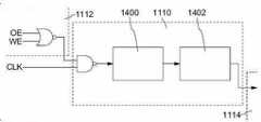
리프레쉬 제어 회로(1110)와, 리프레쉬 제어 회로(1110)에 관련하는 회로의 상세한 구성을 도 4a 내지 도 4c에 도시한다.4A to 4C show detailed configurations of the
도 4a는 리프레쉬 제어 회로(1110) 등의 일례이다. 도 4a에 도시하는 리프레쉬 제어 회로(1110)는 NAND 회로와 리프레쉬용 카운트 회로(1400)와 어드레스 생성 회로(1402)를 갖는다. NAND 회로는 제 2 클록 신호 CLK와, 기록 인에이블 신호 WE와 출력 인에이블 신호 OE의 부정 논리합으로부터, 이들 입력 신호의 부정 논리곱을 출력한다. 리프레쉬용 카운트 회로(1400)는 NAND 회로로부터의 신호에 따라 행 수를 카운트하고, 어드레스 생성 회로(1402)는 리프레쉬용 카운트 회로(1400)에서 카운트된 데이터에 따라 어드레스 신호를 생성하고, 어드레스 제어 회로(1114)에 출력한다. 상기 구성을 사용하는 경우, 기록 인에이블 신호 WE와 출력 인에이블 신호 OE가 비(非)액티브 상태인 경우에 제 2 클록 신호 CLK가 리프레쉬용 카운트 회로(1400)를 동작시키고 행마다 리프레쉬 동작을 행한다. 메모리에 액세스될 때는 리프레쉬 동작이 행해지지 않기 때문에, 리프레쉬되는 간격이 길어지는 경향이 있지만, 개시하는 발명에 따른 반도체 장치에서는 오랜 기간 동안 데이터를 유지할 수 있어서 문제가 되지 않는다.4A is an example of the
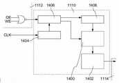
도 4b는 리프레쉬 제어 회로(1110) 등의 다른 일례이다. 도 4b에 도시하는 리프레쉬 제어 회로(1110)는 리프레쉬용 카운트 회로(1400)와 어드레스 생성 회로(1402)와 주파수 검지 회로(1404)와 전환 제어 회로(1406)와 리프레쉬 클록 생성 회로(1408)를 갖는다. 주파수 검지 회로(1404)는 제 2 클록 신호 CLK가 소정의 주파수를 갖는지를 판정하는 회로이고, 대표적으로는 밴드 패스 필터(band pass filter)가 사용된다. 전환 제어 회로(1406)는 주파수 검지 회로(1404)로부터의 신호에 따라 리프레쉬용 카운트 회로(1400)에 제 2 클록 신호 CLK를 직접 입력하는지, 또는 리프레쉬 클록 생성 회로(1408)에 출력하는지를 결정한다. 리프레쉬 클록 생성 회로(1408)는 내부 클록에 의해 리프레쉬 동작에 필요한 주파수의 클록 신호를 생성하고, 리프레쉬용 카운트 회로(1400)에 출력한다. 리프레쉬용 카운트 회로(1400)와 어드레스 생성 회로(1402)의 기능은 도 4a의 경우와 마찬가지다. 상기 구성에서는 제 2 클록 신호 CLK가 리프레쉬 동작에 적합한지 아닌지를 판정하고, 리프레쉬 동작에 적합한 주파수의 클록 신호를 사용하기 때문에, 제 2 클록 신호 CLK의 주파수가 변동하는 경우라도 적절한 리프레쉬 동작을 행할 수 있다.4B is another example of the
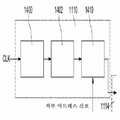
도 4c는 리프레쉬 제어 회로(1110) 등의 다른 일례이다. 도 4c에 도시하는리프레쉬 제어 회로(1110)는 리프레쉬용 카운트 회로(1400)와 어드레스 생성 회로(1402)와 리프레쉬 어드레스 비교 제어 회로(1410)를 갖는다. 리프레쉬 어드레스 비교 제어 회로(1410)는 어드레스 생성 회로(1402)에서 생성되는 어드레스 신호와 외부 어드레스 신호(기록 또는 판독에 관한 어드레스를 지정하는 어드레스 신호)를 비교하여 비교 결과를 어드레스 제어 회로 (1114)에 출력한다. 상기 구성에서는 어드레스 생성 회로(1402)에서 생성되는 어드레스 신호와, 와부 어드레스 신호가 일치되지 않는 경우에 리프레쉬 동작을 행한다.4C is another example of the
다만, 개시하는 발명은 상술한 리프레쉬 제어 회로(1110) 등의 구체적인 구성에 한정되지 않는다.However, the disclosed invention is not limited to the specific configuration of the above-described
<반도체 장치의 동작 1><Operation of
다음에, 상술한 반도체 장치의 기록 동작, 판독 동작 및 리프레쉬 동작의 일례에 대하여 설명한다. 또한, 여기서는 이해하기 쉽게 하기 위하여, 2행×2열의 메모리 셀 어레이로 구성되는 반도체 장치의 동작에 대하여 설명하지만, 개시하는 발명은 이것에 한정되지 않는다.Next, examples of the write operation, read operation, and refresh operation of the semiconductor device described above will be described. In addition, in order to make it easy to understand here, operation | movement of the semiconductor device comprised by the memory cell array of 2 rows x 2 columns is demonstrated, but the invention disclosed is not limited to this.
제 1행 제 1열의 메모리 셀(1200)(1,1) 및 제 1행 제 2열의 메모리 셀(1200)(1,2)에 기록하는 경우와, 제 1행 1열의 메모리 셀(1200)(1,1) 및 제 1행 제 2열의 메모리 셀(1200)(1,2)로부터 판독하는 경우에 대하여 설명한다. 또한, 이하에서는 메모리 셀(1200)(1,1)에 기록하는 데이터를 "1"로 하고, 메모리 셀(1200)(1,2)에 기록하는 데이터를 "0"으로 한다.When writing to the memory cells 1200 (1,1) of the first row and the first column and the memory cells 1200 (1,2) of the first row and the second column, and the
기록 동작에 대하여 설명한다. 우선, 제 1 행째 신호선 S_1에 전위 V1을 공급하여 1 행째 제 2 트랜지스터를 온 상태로 한다. 또한, 제 2 행째 신호선 S_2에 전위 0V를 공급하여 2 행째 제 2 트랜지스터를 오프 상태로 한다. 또한, 제 1 행째 비트선 BL_1에 전위 V2를 공급하고, 제 2 행째 비트선 BL_2에 전위 0V를 공급한다. 그 결과, 메모리 셀(1200)(1,1)의 노드 FG에는 전위 V2가 인가되고, 메모리 셀(1200)(1,2)의 노드 FG에는 전위 0V가 인가된다. 여기서, 판독 동작을 할 때, 전위 V2는 제 1 트랜지스터의 임계값 전압을 초과하는 전위차를 주는 전위로 한다. 또한, 전위 V2는 전위 V1과 같은 정도 또는 전위 V1 이하로 하는 것이 바람직하다.The recording operation will be described. First, the potential V1 is supplied to the first row signal line S_1 to turn on the first row second transistor. Further, the potential 0 V is supplied to the second row signal line S_2 to turn off the second row second transistor. The potential V2 is supplied to the first row bit line BL_1, and the potential 0V is supplied to the second row bit line BL_2. As a result, the potential V 2 is applied to the node FG of the memory cells 1200 (1, 1), and the potential 0 V is applied to the node FG of the memory cells 1200 (1, 2). Here, during the read operation, the potential V2 is a potential that gives a potential difference exceeding the threshold voltage of the first transistor. In addition, the potential V2 is preferably about the same as the potential V1 or lower than the potential V1.
그리고, 제 1 행째 신호선 S_1의 전위를 0V로 하여 1 행째 제 2 트랜지스터를 오프 상태로 함으로써 기록이 종료된다. 또한, 기록 동작 동안 제 1 행째 워드선 WL_1 및 제 2 행째 워드선 WL_2는 전위 0V로 한다. 또한, 기록이 종료될 때는 제 1 행째 비트선 BL_1의 전위를 변화시키기 전에 제 1 행째 신호선 S_1의 전위를 0V로 한다.Then, writing is terminated by turning off the first row second transistor with the potential of the first row signal line S_1 at 0V. In addition, during the write operation, the first row word line WL_1 and the second row word line WL_2 have a potential of 0V. At the end of writing, the potential of the first row signal line S_1 is set to 0V before the potential of the first row bit line BL_1 is changed.
기록 후, 메모리 셀의 임계값은 데이터 "0"의 경우에는 Vw0, 데이터 "1"의 경우에는 Vw1이 된다. 여기서, 메모리 셀의 임계값이란 제 1 트랜지스터의 소스 전극과 드레인 전극 사이의 저항 상태가 변화하는 워드선 WL의 전위를 가리키는 것으로 한다. 또한, 여기서는 Vw0>0>Vw1로 한다.After writing, the threshold value of the memory cell is Vw0 for data "0" and Vw1 for data "1". Here, the threshold of the memory cell refers to the potential of the word line WL in which the resistance state between the source electrode and the drain electrode of the first transistor changes. In this case, Vw0> 0> Vw1.
다음에, 판독 동작에 대하여 설명한다. 우선, 제 1 행째 워드선 WL_1에 전위 0V를 인가하고, 제 2 행째 워드선 WL_2에 전위 VL을 인가한다. 전위 VL은 임계값 Vw1보다 낮은 전위로 한다. 워드선 WL_1을 전위 0V로 하면, 제 1 행째에서 데이터 "0"이 유지되는 메모리 셀의 제 1 트랜지스터는 오프 상태, 데이터 "1"이 유지되는 메모리 셀의 제 1 트랜지스터는 온 상태가 된다. 워드선 WL_2를 전위 VL로 하면, 제 2 행째에서 데이터 "0", 데이터 "1" 중 어느 것이 유지되는 메모리 셀이라도 제 1 트랜지스터는 오프 상태가 된다.Next, the read operation will be described. First, the potential 0 V is applied to the first row word line WL_1, and the potential V L is applied to the second row word line WL_2. The potential VL is set to a potential lower than the threshold value Vw1. When the word line WL_1 has a potential of 0 V, the first transistor of the memory cell in which the data "0" is held in the first row is turned off, and the first transistor of the memory cell in which the data "1" is held is turned in. When the word line WL_2 is set at the potential VL, the first transistor is turned off even in a memory cell in which either data "0" or data "1" is held in the second row.
그래서, 비트선 BL_1과 소스선 SL 사이는 메모리 셀(1200)(1,1)의 제 1 트랜지스터가 온 상태이기 때문에 저저항 상태가 되고, 비트선 BL_2와 소스선 SL 사이는 메모리 셀(1200)(1,2)의 제 1 트랜지스터가 오프 상태이기 때문에 고저항 상태가 된다. 비트선 BL_1, 비트선 BL_2에 접속되는 판독 회로는 비트선의 저항 상태의 차이에 의하여 데이터를 판독한다.Thus, the bit transistor BL_1 and the source line SL are in a low resistance state because the first transistors of the
또한, 판독 동작 동안 신호선 S_1에는 전위 0V를 공급하고 신호선 S_2에는 전위 VL을 공급하여, 제 2 트랜지스터를 모두 오프 상태로 한다. 제 1 행째 메모리 셀에서, 노드 FG의 전위는 0V 또는 V2이기 때문에, 신호선 S_1을 전위 0V로 함으로써 제 2 트랜지스터를 모두 오프 상태로 할 수 있다. 한편, 2 행째의 노드 FG의 전위는 워드선 WL_2에 전위 VL이 공급되면, 기록 직후의 전위보다 낮은 전위가 된다. 이것에 기인하여 제 2 트랜지스터가 온 상태가 되는 것을 방지하기 위하여, 신호선 S_2를 워드선 WL_1과 같은 전위(전위 VL)로 한다. 즉, 판독하지 않는 행에서는 신호선 S과 워드선 WL을 같은 전위(전위 VL)로 한다. 상술한 바와 같이 하여, 제 2 트랜지스터를 모두 오프 상태로 할 수 있다.In addition, during the read operation, the potential 0 V is supplied to the signal line S_1 and the potential VL is supplied to the signal line S_2 to turn off all of the second transistors. In the first row of memory cells, the potential of the node FG is 0V or V2, so that the second transistor can be turned off by setting the signal line S_1 to the potential 0V. On the other hand, when the potential VL is supplied to the word line WL_2, the potential of the node FG in the second row becomes lower than the potential immediately after writing. Due to this, in order to prevent the second transistor from being turned on, the signal line S_2 is set to the same potential (potential VL) as the word line WL_1. In other words, the signal line S and the word line WL have the same potential (potential VL) in the non-reading row. As described above, all of the second transistors can be turned off.
판독 회로로서 도 3에 도시하는 회로를 사용하는 회로를 사용하는 경우에는, 스위치 소자(1206)를 비도통 상태로 하고 스위치 소자(1300)를 도통 상태로 하여 판독할 수 있는 상태로 한다. 소스선 SL에는 정전위(예를 들어 0V)를 공급하고, 또한, 판독 대상인 메모리 셀(1200)이 접속되는 비트선 BL의 스위치 소자(1202)를 도통 상태로 하고 비트선 BL의 프리차지(precharge)를 행한다. 또한, 스위치 소자(1206)를 비도통 상태로 하고 스위치 소자(1302)를 도통 상태로 하고 데이터선을 사용하여 프리차지를 행할 수도 있다. 비트선 BL과 소스선 SL 사이가 저저항 상태인 경우에는 증폭 회로(1204)에는 저전위가 입력되어 데이터 신호 OUTPUT는 저전위가 된다. 비트선 BL과 소스선 SL 사이가 고저항 상태인 경우에는, 증폭 회로(1204)에는 고전위가 입력되어 데이터 신호 OUTPUT는 고전위가 된다.When using the circuit using the circuit shown in FIG. 3 as a read circuit, it is set as the state which can be read by making the
다음에, 리프레쉬 동작의 예에 대하여 설명한다. 개시하는 발명에 따른 반도체 장치에서는 매우 오랜 기간 동안 데이터를 유지할 수 있기 때문에 리프레쉬 동작의 빈도는, 예를 들어 일반적인 DRAM 등의 1/1000 이하, 바람직하게는 1/10000 이하가 된다. 더 구체적으로는 개시하는 발명에 따른 반도체 장치에서는 메모리 셀당 리프레쉬 동작을 103초에 한 번 이하, 바람직하게는 104초에 한 번 이하로 할 수 있다. 따라서, 개시하는 발명에 따른 반도체 장치에서는 리프레쉬 동작에 기인한 전력의 소비를 충분히 억제할 수 있다.Next, an example of the refresh operation will be described. In the semiconductor device according to the disclosed invention, since the data can be held for a very long time, the frequency of the refresh operation is, for example, 1/1000 or less, preferably 1/10000 or less of a general DRAM or the like. More specifically, in the semiconductor device according to the disclosed invention, the refresh operation per memory cell can be made no more than once every 103 seconds, preferably no more than once every 104 seconds. Therefore, in the semiconductor device according to the disclosed invention, power consumption due to the refresh operation can be sufficiently suppressed.
우선, 리프레쉬 대상의 메모리 셀(1200)이 접속되는 비트선 BL의 스위치 소자(1202)를 도통 상태로 하여 비트선 BL을 프리차지한다. 또한, 여기서는 비트선 BL의 프리차지를 판독 회로와 독립된 배선을 사용하여 행하지만, 비트선 BL의 프리차지는 판독 회로(1102)와 공통하는 배선을 사용하여 판독 회로(1102) 측으로부터 행하여도 좋다. 예를 들어, 판독 회로로서 도 3에 도시하는 회로를 사용하는 경우에는, 데이터선을 사용하여 프리차지할 수 있다.First, the bit line BL is precharged with the
다음에, 스위치 소자(1202)를 비도통 상태로 하여 비트선 BL을 플로팅 상태로 한다. 이 상태에서 리프레쉬 대상인 메모리 셀(1200)의 제 2 트랜지스터가 온 상태가 되는 전위를 리프레쉬 대상인 메모리 셀(1200)이 접속되는 신호선에 인가한다. 이로써, 비트선의 전위는 노드 FG에 유지되는 전하량에 따라 변동한다. 판독 회로(1102)의 증폭 회로(1204)는 이 변동을 증폭하여 전위 0V 또는 전위 V2로 하여 출력한다.Next, the bit line BL is in a floating state with the
여기서, 증폭 회로(1204)의 출력과 비트선을 접속하는 스위치 소자(1206)를 도통 상태로 하면, 전위 0V 또는 전위 V2가 비트선에 공급된다. 리프레쉬 대상인 메모리 셀(1200)의 제 2 트랜지스터는 온 상태이기 때문에, 리프레쉬 대상인 메모리 셀(1200)에는 노드 FG에 유지된 전하에 따라, 같은 데이터가 다시 기록된다.Here, when the
<반도체 장치의 동작 2><Operation of Semiconductor Device 2>
다음에, 반도체 장치의 동작의 다른 일례에 대하여 설명한다. 또한, 여기서는 이해를 쉽게 하기 위하여 2행×2열의 메모리 셀 어레이로 구성되는 반도체 장치의 동작에 대하여 설명한다. 또한, 기록하는 데이터는 상술한 기록 동작과 같게 한다.Next, another example of the operation of the semiconductor device will be described. In addition, in order to make it easy to understand, the operation | movement of the semiconductor device comprised from the memory cell array of 2 rows x 2 columns is demonstrated here. The data to be recorded is made the same as the above-described recording operation.
<반도체 장치의 동작 1>에 제시하는 기록(1 행째 기록)에서는 기록 시의 워드선 WL_2의 전위를 전위 0V로 설정하기 때문에, 예를 들어 메모리 셀(1200)(2,1) 또는 메모리 셀(1200)(2,2)에 기록된 데이터가 "1"인 경우에는 비트선 BL_1과 비트선 BL_2 사이에 정상 전류가 흐를 우려가 있다. 제 1 행째를 기록할 때는 제 2 행째 메모리 셀이 갖는 제 1 트랜지스터가 온 상태가 되어, 비트선 BL_1과 비트선 BL_2가 소스선을 통하여 저저항으로 접속되기 때문이다. 여기서 제시하는 기록 동작은 이러한 정상 전류의 발생을 방지하는 방법이다.In the write (first row write) shown in <
우선, 제 1 행째 신호선 S_1에 전위 V1을 공급하여, 1 행째 제 2 트랜지스터를 온 상태로 한다. 또한, 제 2 행째 신호선 S_2에 전위 0V를 공급하여, 2 행째 제 2 트랜지스터를 오프 상태로 한다. 또한, 제 1 행째 비트선 BL_1에 전위 V2를 공급하고, 제 2 행째 비트선 BL_2에 전위 0V를 공급한다. 그렇기 때문에, 메모리 셀(1200)(1,1)의 노드 FG에는 전위 V2가 공급되고, 메모리 셀(1200)(1,2)의 노드 FG에는 전위 0V가 공급된다. 여기서는, 전위 V2는 제 1 트랜지스터의 임계값 전압을 초과하는 전위차를 주는 전위로 한다. 그리고, 제 1 행째 신호선 S_1의 전위를 0V로 하여, 1 행째 제 2 트랜지스터를 오프 상태로 함으로써 기록이 종료된다.First, the potential V1 is supplied to the first row signal line S_1 to turn on the first row second transistor. Further, the potential 0 V is supplied to the second row signal line S_2 to turn off the second row second transistor. The potential V2 is supplied to the first row bit line BL_1, and the potential 0V is supplied to the second row bit line BL_2. Therefore, the potential V 2 is supplied to the node FG of the memory cells 1200 (1, 1), and the potential 0 V is supplied to the node FG of the memory cells 1200 (1, 2). Here, the potential V 2 is a potential giving a potential difference exceeding the threshold voltage of the first transistor. The recording is terminated by setting the potential of the first row signal line S_1 to 0V and turning off the first row second transistor.
또한, 기록 동작 동안 제 1 행째 워드선 WL_1의 전위는 전위 0V로 하고, 제 2 행째 워드선 WL_2의 전위는 전위 VL로 한다. 제 2 행째 워드선 WL_2의 전위는 전위 VL로 함으로써, 제 2 행째에서 데이터 "0" 또는 데이터 "1" 중 어느 쪽이 유지되는 메모리 셀에서도 제 1 트랜지스터는 오프 상태가 된다. 또한, 기록 동작 동안 소스선 SL에는 전위 V2를 인가한다. 기록 데이터가 모두 "0"인 경우에는 소스선에는 전위 0V를 인가하여도 좋다.During the write operation, the potential of the first row word line WL_1 is set at the potential 0V, and the potential of the second row word line WL_2 is set at the potential VL. By setting the potential of the second row word line WL_2 to the potential VL, the first transistor is turned off even in the memory cell in which either the data "0" or the data "1" is held in the second row. In addition, the potential V2 is applied to the source line SL during the write operation. When all the write data are "0", the potential 0V may be applied to the source line.
또한, 기록이 종료될 때는, 제 1 행째 비트선 BL_1의 전위를 변화시키기 전에제 1 행째 신호선 S_1을 전위 0V로 한다. 기록 후에서는, 메모리 셀의 임계값은 데이터 "0"의 경우에는 Vw0, 데이터 "1"의 경우에는 Vw1이 된다. 또한, 여기서는 Vw0>0>Vw1로 한다.When the writing is completed, the first row signal line S_1 is set to the potential 0V before the potential of the first row bit line BL_1 is changed. After writing, the threshold of the memory cell is Vw0 for data "0" and Vw1 for data "1". In this case, Vw0> 0> Vw1.
상기 기록 동작에서 기록을 행하지 않는 행(이 경우에는 제 2 행째)의 메모리 셀의 제 1 트랜지스터는 오프 상태이기 때문에, 비트선과 소스선 사이의 정상 전위가 문제가 되는 것은 기록을 행하는 행의 메모리 셀 뿐이다. 기록을 행하는 행의 메모리 셀에 데이터 "0"을 기록하는 경우에는, 상기 메모리 셀이 갖는 제 1 트랜지스터는 오프 상태가 되기 때문에 정상 전류 문제는 발생하지 않는다. 한편, 기록을 행하는 행의 메모리 셀에 데이터 "1"을 기록하는 경우에는 상기 메모리 셀이 갖는 제 1 트랜지스터는 온 상태가 되기 때문에, 소스선 SL과 비트선 BL(이 경우에는 비트선 BL_1) 사이에 전위차가 존재하는 경우에는 정상 전위가 발생한다. 따라서, 소스선 SL의 전위를 비트선 BL_1의 전위 V2와 같게 함으로써, 비트선과 소스선 사이의 정상 전류를 방지할 수 있다.Since the first transistor of the memory cells in the row (in this case, the second row) that does not write in the write operation is in an off state, the normal potential between the bit line and the source line becomes a problem because the memory cells in the row in which writing is performed. It is only. In the case where data " 0 " is written in the memory cells of the row to be written, the steady state problem does not occur because the first transistor of the memory cell is turned off. On the other hand, when data " 1 " is written to the memory cells of the row to be written, the first transistor of the memory cell is turned on, so that between the source line SL and the bit line BL (bit line BL_1 in this case), If there is a potential difference in, a steady potential occurs. Therefore, by making the potential of the source line SL equal to the potential V2 of the bit line BL_1, it is possible to prevent the steady current between the bit line and the source line.
상술한 바와 같이, 상기 기록 동작에 의하여 기록 시의 정상 전류의 발생을 방지할 수 있다. 즉, 상기 기록 동작에서는 기록 동작시의 소비 전력을 충분히 억제할 수 있다.As described above, the generation of the normal current at the time of writing can be prevented by the writing operation. That is, in the above recording operation, power consumption during the recording operation can be sufficiently suppressed.
또한, 판독 동작, 리프레쉬 동작에서는 상술한 판독 동작, 리프레쉬 동작과 마찬가지다.The read operation and the refresh operation are the same as the read operation and the refresh operation described above.
상술한 바와 같이, 산화물 반도체와 같은, 오프 전류가 매우 작게 되는 재료를 사용함으로써 매우 오랜 기간 동안 기억 내용을 유지할 수 있다. 이로써, 리프레쉬 동작의 빈도를 매우 낮게 하는 것이 가능하기 때문에, 소비 전력을 충분히 저감할 수 있다. 또한, 전력이 공급되지 않는 경우에서도 오랜 기간 동안 기억 내용을 유지할 수 있다.As described above, by using a material in which the off current is very small, such as an oxide semiconductor, the memory contents can be maintained for a very long time. As a result, since the frequency of the refresh operation can be made very low, power consumption can be sufficiently reduced. In addition, the memory contents can be maintained for a long time even when power is not supplied.
또한, 상술한 반도체 장치에서는 정보의 기록에 높은 전압이 필요없고, 소자 열화의 문제도 없다. 그래서, 종래의 비휘발성 메모리에서 문제가 되는 재기록 가능 횟수에 제한이 없고, 신뢰성이 비약적으로 향상된다. 또한, 트랜지스터를 온 상태 또는 오프 상태로 함으로써 정보를 기록하기 때문에, 고속 동작도 용이하게 실현할 수 있다. 또한, 정보를 제거하기 위한 동작이 필요없다는 이점도 있다.In addition, in the semiconductor device described above, a high voltage is not required for recording information, and there is no problem of element deterioration. Therefore, there is no limit to the number of rewritable problems which are a problem in the conventional nonvolatile memory, and the reliability is drastically improved. In addition, since the information is recorded by turning the transistor on or off, high-speed operation can be easily realized. In addition, there is an advantage that an operation for removing information is not necessary.
또한, 동작 속도가 높은 반도체 재료를 사용한 트랜지스터와 오프 전류가 작은 반도체 재료를 사용한 트랜지스터를 조합하여 사용함으로써, 반도체 장치의 동작(예를 들어, 정보의 판독 동작)의 고속성을 충분히 확보할 수 있다. 또한, 동작 속도가 높은 반도체 재료를 사용한 트랜지스터에 의해, 고속 동작이 요구되는 각종 회로(논리 회로, 구동 회로 등)를 적합하게 실현할 수 있다.In addition, by using a combination of a transistor using a semiconductor material having a high operating speed and a transistor using a semiconductor material having a small off current, the high speed of the operation (for example, information read operation) of the semiconductor device can be sufficiently secured. . In addition, the transistor using a semiconductor material having a high operation speed can suitably realize various circuits (logical circuits, drive circuits, etc.) for which high speed operation is required.
본 실시형태에서 제시하는 구성, 방법 등은 다른 실시형태에 제시하는 구성, 방법 등과 적합하게 사용할 수 있다.The structure, method, etc. which are shown in this embodiment can be used suitably for the structure, method, etc. which are shown in another embodiment.
(실시형태 3)(Embodiment 3)
본 실시형태에서는, 본 발명의 일 형태에 따른 반도체 장치의 구성 및 그 제작 방법에 대해서 도 5a 내지 도 9c를 참조하여 설명한다.In this embodiment, the structure and manufacturing method of the semiconductor device of one embodiment of the present invention will be described with reference to FIGS. 5A to 9C.
<반도체 장치의 단면 구성 및 평면 구성><Semiconductor and Planar Configuration of Semiconductor Devices>
도 5a 및 도 5b는, 반도체 장치의 구성의 일례이다. 도 5a에는, 반도체 장치의 단면을 도시하고, 도 5b에는 반도체 장치의 평면을 도시한다. 여기서, 도 5a는 도 5b의 A1-A2 및 B1-B2에서의 단면에 상당한다. 도 5a 및 도 5b에 도시하는 반도체 장치는 하부(下部)에 제 1 반도체 재료를 사용한 트랜지스터(160)를 갖고, 상부(上部)에 제 2 반도체 재료를 사용한 트랜지스터(162)를 갖는다. 여기서, 제 1 반도체 재료와 제 2 반도체 재료는 상이한 재료로 하는 것이 바람직하다. 예를 들어, 제 1 반도체 재료를 산화물 반도체 이외의 반도체 재료로 하고, 제 2 반도체 재료를 산화물 반도체 재료로 할 수 있다. 산화물 반도체 이외의 반도체 재료로서는, 예를 들어 실리콘, 게르마늄, 실리콘게르마늄, 탄화실리콘, 인듐인, 또는 갈륨비소 등을 사용할 수 있고, 단결정 반도체를 사용하는 것이 바람직하다. 이러한 반도체 재료를 사용한 트랜지스터는 고속 동작이 용이하다. 한편, 산화물 반도체를 사용한 트랜지스터는 그 특성에 의해 전하를 오랜 시간 동안 유지할 수 있다.5A and 5B are examples of the configuration of a semiconductor device. FIG. 5A shows a cross section of the semiconductor device, and FIG. 5B shows a plane of the semiconductor device. Here, FIG. 5A is corresponded to the cross section in A1-A2 and B1-B2 of FIG. 5B. The semiconductor device shown in FIGS. 5A and 5B has a
또한, 상기 트랜지스터 중 양쪽 모두는 n채널형 트랜지스터로서 설명하지만, p채널형 트랜지스터를 사용할 수 있는 것은 물론이다. 또한, 개시하는 발명의 기술적인 본질은, 정보를 유지하기 위해서 산화물 반도체와 같은 오프 전류를 충분히 저감할 수 있는 반도체 재료를 트랜지스터(162)에 사용하는 점에 있기 때문에, 반도체 장치에 사용되는 재료나 반도체 장치의 구조 등, 반도체 장치의 구체적인 구성은 여기서 제시하는 것에 한정할 필요는 없다.Note that both of the above transistors are described as n-channel transistors, but of course, p-channel transistors can be used. In addition, since the technical nature of the disclosed invention is that the
도 5a 및 도 5b에 도시하는 트랜지스터(160)는 제 1 반도체 재료(예를 들어, 실리콘 등)를 포함하는 기판(100)에 형성된 채널 형성 영역(116)과, 채널 형성 영역(116)을 끼우도록 형성된 불순물 영역(120)과, 불순물 영역(120)에 접하는 금속 화합물 영역(124)과, 채널 형성 영역(116) 위에 형성된 게이트 절연층(108)과, 게이트 절연층(108) 위에 형성된 게이트 전극(110)을 갖는다. 또한, 도면에 있어서, 명시적(明示的)으로는 소스 전극이나 드레인 전극을 갖지 않는 경우가 있지만, 편의상 이와 같은 상태를 포함하여 트랜지스터라고 부르는 경우가 있다. 또한, 이 경우에는, 트랜지스터의 접속 관계를 설명하기 위해서 소스 영역이나 드레인 영역을 포함하여 소스 전극이나 드레인 전극이라고 표현할 수 있다. 즉, 본 명세서에 있어서, 소스 전극이라는 기재는 소스 영역을 포함한다.The
트랜지스터(160)의 금속 화합물 영역(124)의 일부에는 전극(126)이 접속된다. 여기서, 전극(126)은 트랜지스터(160)의 소스 전극이나 드레인 전극으로서 기능한다. 또한, 기판(100) 위에는 트랜지스터(160)를 둘러싸도록 소자 분리 절연층(106)이 형성되고, 트랜지스터(160)를 덮어 절연층(128)이 형성된다. 또한, 고집적화를 실현하기 위해서는, 도 5a 및 도 5b에 도시하는 바와 같이, 트랜지스터(160)가 사이드월 절연층을 갖지 않는 구성으로 하는 것이 바람직하다. 한편, 트랜지스터(160)의 특성을 중요시하는 경우에는, 게이트 전극(110)의 측면에 사이드월 절연층을 형성하고, 그 사이드월 절연층과 중첩되는 영역에 형성된 불순물 농도가 상이한 영역을 포함하여 불순물 영역(120)을 형성하여도 좋다.An
도 5a 및 도 5b에 도시하는 트랜지스터(162)는 절연층(128) 위에 형성된 소스 전극 또는 드레인 전극(142a), 및 소스 전극 또는 드레인 전극(142b)과, 소스 전극 또는 드레인 전극(142a), 및 소스 전극 또는 드레인 전극(142b)과 전기적으로 접속되는 산화물 반도체층(144)과, 소스 전극 또는 드레인 전극(142a), 소스 전극 또는 드레인 전극(142b), 산화물 반도체층(144)을 덮는 게이트 절연층(146)과, 게이트 절연층(146) 위에 산화물 반도체층(144)과 중첩하도록 형성된 게이트 전극(148)을 갖는다.The
여기서, 산화물 반도체층(144)은 수소 등의 불순물이 충분히 제거됨으로써, 또는 충분한 산소가 공급됨으로써, 고순도화된 것이 바람직하다. 수소 농도가 충분히 저감되어 고순도화되고, 충분한 산소가 공급됨으로써 산소 결핍(缺乏)에 기인한 에너지 갭 내의 결함 준위가 저감된 산화물 반도체층(144)에서는 캐리어 농도가 1×10¹²/cm3 미만, 바람직하게는 1×10¹¹/cm3 미만, 더 바람직하게는 1.45×10¹⁰/cm3 미만이 된다. 예를 들어, 실온(25℃)에서의 오프 전류(여기서는 단위 채널 폭(1μm)당 값)는 10zA(1zA는 1×10-21A) 이하, 바람직하게는 1zA 이하가 된다. 이와 같이, i형화(진성화) 또는 실질적으로 i형화된 산화물 반도체를 사용함으로써, 매우 우수한 오프 전류 특성을 갖는 트랜지스터(162)를 얻을 수 있다.Here, the
도 5a 및 도 5b에 도시하는 용량 소자(164)는 소스 전극 또는 드레인 전극(142a), 산화물 반도체층(144), 게이트 절연층(146), 절연층(150) 및 전극(149)으로 구성된다. 즉, 소스 전극 또는 드레인 전극(142a)은 용량 소자(164)의 한쪽의 전극으로서 기능하고, 전극(149)은 용량 소자(164)의 다른 쪽의 전극으로서 기능한다.The
또한, 도 5a 및 도 5b에 도시하는 용량 소자(164)에서는 산화물 반도체층(144), 게이트 절연층(146) 및 절연층(150)을 적층시킴으로써, 소스 전극 또는 드레인 전극(142a)과 전극(149) 사이의 절연성을 충분히 확보할 수 있다. 또한, 충분한 용량을 확보하기 위해서 게이트 절연층(146) 및 절연층(150) 중 한쪽을 갖지 않는 구성의 용량 소자(164)를 채용하여도 좋다. 또한, 산화물 반도체층(144)을 갖지 않는 구성의 용량 소자(164)를 채용하여도 좋다.In the
본 실시형태에 제시하는 구성에서는 트랜지스터(160)와 트랜지스터(162)가 적어도 일부가 중첩되도록 형성된다. 또한, 트랜지스터(162)나 용량 소자(164)가 트랜지스터(160)과 중첩하도록 형성된다. 예를 들어, 용량 소자(164)의 전극(149)은 트랜지스터(162)의 게이트 전극(148)과 적어도 일부가 중첩되어 형성된다. 또한, 용량 소자(164)의 전극(149)은 트랜지스터(160)의 게이트 전극(110)과 적어도 일부분이 중첩되도록 형성되는 구성으로 하여도 좋다. 이와 같은 평면 레이아웃을 채용함으로써, 고집적화할 수 있다. 예를 들어, 최소 가공 치수를 F로 하고, 메모리 셀이 차지하는 면적을 9F2 내지 25F2로 할 수 있다.In the structure shown in this embodiment, the
게이트 전극(148)을 덮도록 절연층(150)이 형성되고, 트랜지스터(162) 및 용량 소자(164) 위에는 절연층(151)이 형성되고, 절연층(151) 위에는 절연층(152)이 형성된다. 그리고, 게이트 절연층(146), 절연층(150), 절연층(151), 절연층(152) 등에 형성된 개구에는 전극(154)이 형성되고, 절연층(152) 위에는 전극(154)과 접속하는 배선(156)이 형성된다. 또한, 도 5a 및 도 5b에서는, 전극(126) 및 전극(154)을 사용하여 금속 화합물 영역(124), 소스 전극 또는 드레인 전극(142b), 및 배선(156)을 접속하지만, 개시하는 발명은 이것에 한정되지 않는다. 예를 들어, 소스 전극 또는 드레인 전극(142b)을 금속 화합물 영역(124)에 직접 접촉시켜도 좋다. 또는, 배선(156)을 소스 전극 또는 드레인 전극(142b)에 직접 접촉시켜도 좋다.An insulating
또한, 도 5a 및 도 5b에서 금속 화합물 영역(124)과 소스 전극 또는 드레인 전극(142b)을 접속하는 전극(126)과, 소스 전극 또는 드레인 전극(142b)과 배선(156)을 접속하는 전극(154)은 중첩되어 배치된다. 즉, 트랜지스터(160)의 소스 전극이나 드레인 전극(142b)으로서 기능하는 전극(126)과 트랜지스터(162)의 소스 전극 또는 드레인 전극(142b)이 접하는 영역은 트랜지스터(162)의 소스 전극 또는 드레인 전극(142b)과, 하나의 메모리 셀과 다른 메모리 셀을 접속하는 배선(156)이 접하는 영역과 겹친다. 이러한 레이아웃을 채용함으로써, 고집적화를 도모할 수 있다. 물론, 상기 구성은 일례이기 때문에 개시하는 발명을 상기 구성에 한정할 필요는 없다.5A and 5B, an
<반도체 장치의 제작 방법><Method of manufacturing semiconductor device>
다음에, 상기 반도체 장치의 제작 방법의 일례에 대해서 설명한다. 이하에서는, 먼저 하부 트랜지스터(160)의 제작 방법에 대해서 도 6a 내지 도 7c를 참조하여 설명하고, 그 후 상부 트랜지스터(162) 및 용량 소자(164)의 제작 방법에 대해서 도 8a 내지 도 9c를 참조하여 설명한다.Next, an example of the manufacturing method of the said semiconductor device is demonstrated. Hereinafter, a method of manufacturing the
<하부 트랜지스터의 제작 방법><Method of manufacturing lower transistor>
우선, 제 1 반도체 재료를 포함하는 기판(100)을 준비한다(도 6a 참조). 제 1 반도체 재료를 포함하는 기판(100)으로서는, 실리콘이나 탄화실리콘 등의 단결정 반도체 기판, 다결정 반도체 기판, 실리콘게르마늄 등의 화합물 반도체 기판, SOI 기판 등을 적용할 수 있다. 여기서는, 제 1 반도체 재료를 포함하는 기판(100)으로서, 단결정 실리콘 기판을 사용하는 경우의 일례에 대해서 제시한다. 또한, 일반적으로는 "SOI 기판"이란 절연 표면 위에 실리콘 반도체층이 형성된 구성의 기판을 말하지만, 본 명세서 등에 있어서의 개념으로서는, 절연 표면 위에 실리콘 이외의 재료로 이루어진 반도체층이 형성된 구성의 기판도 포함한다. 즉, "SOI 기판"이 갖는 반도체층은 실리콘 반도체층에 한정되지 않는다. 또한, SOI 기판에는 유리 기판 등의 절연 기판 위에 절연층을 개재하여 반도체층이 형성된 구성이 포함된다.First, the
또한, 제 1 반도체 재료를 포함하는 기판(100)으로서, 특히 실리콘 등의 단결정 반도체 기판을 사용하는 경우에는, 반도체 장치의 판독 동작을 고속화할 수 있기 때문에 적합하다.Moreover, especially when using a single crystal semiconductor substrate, such as silicon, as the board |
기판(100) 위에는 소자 분리 절연층을 형성하기 위한 마스크가 되는 보호층(102)을 형성한다(도 6a 참조). 보호층(102)으로서는, 예를 들어 산화실리콘이나 질화실리콘, 산화질화실리콘 등을 재료로 하는 절연층을 사용할 수 있다. 또한, 이 공정의 전후(前後)에서, 트랜지스터의 임계값 전압을 제어하기 위해서 n형 도전성을 부여하는 불순물 원소나 p형 도전성을 부여하는 불순물 원소를 기판(100)에 첨가하여도 좋다. 반도체가 실리콘인 경우, n형 도전성을 부여하는 불순물 원소로서는, 예를 들어 인이나 비소 등을 사용할 수 있다. 또한, p형 도전성을 부여하는 불순물 원소로서는, 예를 들어 붕소, 알루미늄, 갈륨 등을 사용할 수 있다.A protective layer 102 serving as a mask for forming an element isolation insulating layer is formed on the substrate 100 (see FIG. 6A). As the protective layer 102, for example, an insulating layer made of silicon oxide, silicon nitride, silicon oxynitride, or the like can be used. In addition, before and after this step, in order to control the threshold voltage of the transistor, an impurity element imparting n-type conductivity or an impurity element imparting p-type conductivity may be added to the
다음에, 상기 보호층(102)을 마스크로 하여 에칭을 행하고, 보호층(102)이 덮지 않는 영역(노출되는 영역)의 기판(100)의 일부를 제거한다. 이로써, 다른 반도체 영역과 분리된 반도체 영역(104)이 형성된다(도 6b 참조). 상기 에칭에는, 드라이 에칭을 사용하는 것이 바람직하지만, 웨트 에칭을 사용하여도 좋다. 에칭 가스나 에칭 용액에 대해서는 피(被)에칭 재료에 따라 적절히 선택할 수 있다.Next, etching is performed using the protective layer 102 as a mask to remove a portion of the
다음에, 반도체 영역(104)을 덮도록 절연층을 형성하고, 반도체 영역(104)에 중첩하는 영역의 절연층을 선택적으로 제거함으로써, 소자 분리 절연층(106)을 형성한다(도 6c 참조). 상기 절연층은 산화실리콘이나 질화실리콘, 산화질화실리콘 등을 사용하여 형성된다. 절연층을 제거하는 방법으로서는, CMP(화학적 기계적 연마) 등의 연마 처리나 에칭 처리 등이 있지만, 그 중에서 어느 처리법을 사용하여도 좋다. 또한, 반도체 영역(104)을 형성한 후, 또는 소자 분리 절연층(106)을 형성한 후에는 상기 보호층(102)을 제거한다.Next, the insulating layer is formed so as to cover the
여기서, CMP 처리란 피가공물의 표면을 기준으로 하고, 그것에 따라 표면을 화학적 기계적인 복합 작용으로 평탄화하는 수법이다. 더 구체적으로는, 연마대 위에 연마포를 부착하고, 피가공물과 연마포 사이에 슬러리(연마제)를 공급하면서 연마대와 피가공물을 각각 회전 또는 요동시켜 슬러리와 피가공물 표면 사이에서의 화학 반응 및 연마포와 피가공물의 기계적 연마의 작용으로 피가공물의 표면을 연마하는 방법이다.Here, the CMP treatment is a method of flattening the surface by chemical mechanical complex action based on the surface of the workpiece. More specifically, a polishing cloth is attached on the polishing table, and the polishing table and the workpiece are rotated or oscillated while supplying a slurry (polishing agent) between the workpiece and the polishing cloth, respectively, so that the chemical reaction between the slurry and the workpiece surface and A method of polishing a surface of a workpiece by the action of mechanical polishing of the polishing cloth and the workpiece.
또한, 소자 분리 절연층(106)의 형성 방법으로서 절연층을 선택적으로 제거하는 방법 외, 산소를 도입함으로써 절연성 영역을 형성하는 방법 등을 사용할 수도 있다.As the method for forming the element
다음에, 반도체 영역(104) 표면에 절연층을 형성하고, 상기 절연층 위에 도전 재료를 포함하는 층을 형성한다.Next, an insulating layer is formed on the surface of the
절연층은 나중에 게이트 절연층이 되는 층이며, 예를 들어 반도체 영역(104) 표면의 열처리(열산화 처리나 열질화 처리 등)에 의해 형성할 수 있다. 열처리 대신에 고밀도 플라즈마 처리를 적용하여도 좋다. 고밀도 플라즈마 처리는, 예를 들어 He, Ar, Kr, Xe 등의 희 가스, 산소, 산화질소, 암모니아, 질소, 수소 등 중의 어느 것의 혼합 가스를 사용하여 행할 수 있다. 물론, CVD법이나 스퍼터링법 등을 사용하여 절연층을 형성하여도 좋다. 상기 절연층은, 산화실리콘, 산화질화실리콘, 질화실리콘, 산화하프늄, 산화알루미늄, 산화탄탈, 산화이트륨, 하프늄실리케이트(HfSixOy(x>0, y>0)), 질소가 첨가된 하프늄실리케이트(HfSixOy(x>0, y>0), 질소가 첨가된 하프늄알루미네이트(HfAlxOy(x>0, y>0)) 등을 포함하는 단층 구조 또는 적층 구조로 하는 것이 바람직하다. 또한, 절연층의 두께는 예를 들어, 1nm 이상 100nm 이하, 바람직하게는 10nm 이상 50nm 이하로 할 수 있다.The insulating layer is a layer which later becomes a gate insulating layer, and can be formed, for example, by heat treatment (thermal oxidation treatment, thermal nitriding treatment, etc.) of the surface of the
도전 재료를 포함하는 층은 알루미늄이나 구리, 티타늄, 탄탈, 텅스텐 등의 금속 재료를 사용하여 형성할 수 있다. 또한, 다결정 실리콘 등의 반도체 재료를 사용하여 도전 재료를 포함하는 층을 형성하여도 좋다. 형성 방법도 특별히 한정되지 않고, 증착법, CVD법, 스퍼터링법, 스핀 코팅법 등의 각종 성막 방법을 사용할 수 있다. 또한, 본 실시형태에서는 도전 재료를 포함하는 층을 금속 재료를 사용하여 형성하는 경우의 일례에 대해서 제시한다.The layer containing the conductive material can be formed using a metal material such as aluminum, copper, titanium, tantalum or tungsten. Further, a layer containing a conductive material may be formed using a semiconductor material such as polycrystalline silicon. The formation method is not particularly limited, and various deposition methods such as a vapor deposition method, a CVD method, a sputtering method, and a spin coating method can be used. In addition, in this embodiment, the example at the time of forming the layer containing an electrically-conductive material using a metal material is shown.
그 후, 절연층 및 도전 재료를 포함하는 층을 선택적으로 에칭하여 게이트 절연층(108), 게이트 전극(110)을 형성한다(도 6c 참조).Thereafter, the layer including the insulating layer and the conductive material is selectively etched to form the
다음에, 반도체 영역(104)에 인(P)이나 비소(As) 등을 첨가하여 채널 형성 영역(116) 및 불순물 영역(120)을 형성한다(도 6d 참조). 또한, 여기서는 n형 트랜지스터를 형성하기 위해서 인이나 비소를 첨가하지만, p형 트랜지스터를 형성하는 경우에는 붕소(B)나 알루미늄(Al) 등의 불순물 원소를 첨가하면 좋다. 여기서, 첨가하는 불순물의 농도는 적절히 설정할 수 있지만, 반도체 소자가 고도로 미세화되는 경우에는, 그 농도를 높게 하는 것이 바람직하다.Next, phosphorus (P), arsenic (As), or the like is added to the
또한, 게이트 전극(110)의 주위에 사이드월 절연층을 형성하고, 불순물 원소가 상이한 농도로 첨가된 불순물 영역을 형성하여도 좋다.In addition, a sidewall insulating layer may be formed around the
다음에, 게이트 전극(110), 불순물 영역(120) 등을 덮도록 금속층(122)을 형성한다(도 7a 참조). 상기 금속층(122)은 진공 증착법이나 스퍼터링법, 스핀 코팅법 등의 각종 성막 방법을 사용하여 형성할 수 있다. 금속층(122)은 반도체 영역(104)을 구성하는 반도체 재료와 반응함으로써 저저항 금속 화합물이 되는 금속 재료를 사용하여 형성하는 것이 바람직하다. 이와 같은 금속 재료로서는, 예를 들어 티타늄, 탄탈, 텅스텐, 니켈, 코발트, 백금 등이 있다.Next, a
다음에, 열처리를 하여 상기 금속층(122)과 반도체 재료를 반응시킨다. 이로써, 불순물 영역(120)에 접하는 금속 화합물 영역(124)이 형성된다(도 7a 참조). 또한, 게이트 전극(110)으로서 다결정 실리콘 등을 사용하는 경우에는, 게이트 전극(110)의 금속층(122)과 접촉하는 부분에도 금속 화합물 영역이 형성된다.Next, heat treatment is performed to react the
상기 열처리로서는, 예를 들어, 플래시 램프 조사에 의한 열처리를 사용할 수 있다. 물론, 그 이외의 열처리 방법을 사용하여도 좋지만, 금속 화합물의 형성시에 일어나는 화학 반응의 제어성을 향상시키기 위해서는, 매우 짧은 시간의 열처리를 실현할 수 있는 방법을 사용하는 것이 바람직하다. 또한, 상술한 금속 화합물 영역은 금속 재료와 반도체 재료의 반응에 의해 형성되는 것이며, 충분히 도전성이 높아진 영역이다. 상기 금속 화합물 영역을 형성함으로써, 전기 저항을 충분히 저감하고 소자 특성을 향상시킬 수 있다. 또한, 금속 화합물 영역(124)을 형성한 후에는, 금속층(122)을 제거한다.As the heat treatment, for example, heat treatment by flash lamp irradiation can be used. Of course, other heat treatment methods may be used. However, in order to improve the controllability of the chemical reaction occurring during the formation of the metal compound, it is preferable to use a method capable of realizing heat treatment for a very short time. In addition, the above-mentioned metal compound region is formed by reaction of a metal material and a semiconductor material, and is a region | region which fully improved electroconductivity. By forming the metal compound region, the electrical resistance can be sufficiently reduced and the device characteristics can be improved. After the
다음에, 금속 화합물 영역(124)의 일부와 접하는 영역에 전극(126)을 형성한다(도 7b 참조). 전극(126)은 예를 들어, 도전 재료를 포함하는 층을 형성한 후에 상기 층을 선택적으로 에칭함으로써 형성된다. 도전 재료를 포함하는 층은 알루미늄이나 구리, 티타늄, 탄탈, 텅스텐 등의 금속 재료를 사용하여 형성할 수 있다. 또한, 다결정 실리콘 등의 반도체 재료를 사용하여 도전 재료를 포함하는 층을 형성하여도 좋다. 형성 방법도 특별히 한정되지 않고, 증착법, CVD법, 스퍼터링법, 스핀코팅법 등의 각종 성막 방법을 사용할 수 있다.Next, an
또한, 절연층(128)을 형성한 후에 절연층(128)에 금속 화합물 영역(124)까지 이르는 개구를 형성하고, 전극(126)을 상기 개구에 매설하도록 형성할 수도 있다.In addition, after the insulating
이 경우, 예를 들어 개구를 포함하는 영역에 PVD법으로 티타늄막을 얇게 형성하고, CVD법으로 질화티타늄막을 얇게 형성한 후에 개구에 매설하도록 텅스텐막을 형성하는 방법을 적용할 수 있다. 여기서, PVD법으로 형성되는 티타늄막은 피형성면의 산화막(자연 산화막 등)을 환원하여, 하부 전극 등(여기서는 금속 화합물 영역(124))과의 접촉 저항을 저감시키는 기능을 갖는다. 또한, 그 후에 형성되는 질화티타늄막은 도전성 재료의 확산을 억제하는 배리어 기능을 갖는다. 또한, 티타늄이나 질화티타늄 등으로 이루어진 배리어막을 형성한 후에 도금법으로 구리막을 형성하여도 좋다.In this case, for example, a method of forming a thin titanium film in the region including the opening by the PVD method, and forming a thin titanium nitride film by the CVD method and then embedding the tungsten film in the opening can be applied. Here, the titanium film formed by the PVD method has a function of reducing an oxide film (natural oxide film or the like) on the surface to be formed to reduce contact resistance with a lower electrode or the like (here, the metal compound region 124). Further, the titanium nitride film formed thereafter has a barrier function of suppressing diffusion of the conductive material. In addition, after forming the barrier film which consists of titanium, titanium nitride, etc., you may form a copper film by the plating method.
다음에, 상술한 공정에 의해 형성된 각 구성을 덮도록 절연층(128)을 형성한다(도 7c 참조). 절연층(128)은 산화실리콘, 산화질화실리콘, 질화실리콘, 산화알루미늄 등의 무기 절연 재료를 포함하는 재료를 사용하여 형성할 수 있다. 특히, 절연층(128)에 유전율이 낮은(low-k) 재료를 사용함으로써, 각종 전극이나 배선 겹침에 기인한 용량을 충분히 저감할 수 있기 때문에 바람직하다. 또한, 절연층(128)에는 이들 재료를 사용한 다공성(多孔性) 절연층을 적용하여도 좋다. 다공성 절연층에서는, 밀도가 높은 절연층과 비교하여 유전율이 낮기 때문에, 전극이나 배선에 기인한 용량을 더 저감할 수 있다. 또한, 절연층(128)은 폴리이미드, 아크릴 등의 유기 절연 재료를 사용하여 형성할 수도 있다. 또한, 여기서는 절연층(128)의 단층 구조로 하지만, 개시하는 발명의 일 형태는 이것에 한정되지 않는다. 2층 이상의 적층 구조로 하여도 좋다.Next, the insulating
상술한 공정에 의해 제 1 반도체 재료를 포함하는 기판(100)을 사용한 트랜지스터(160)가 형성된다(도 7c 참조). 이와 같은 트랜지스터(160)는 고속 동작이 가능하다는 특징을 갖는다. 따라서, 상기 트랜지스터를 판독용 트랜지스터로서 사용함으로써 정보를 고속으로 판독할 수 있다.By the above-described process, the
그 후, 트랜지스터(162) 및 용량 소자(164)를 형성하기 전의 처리로서, 절연층(128)에 CMP 처리를 행하여 게이트 전극(110) 및 전극(126)의 상면을 노출시킨다(도 7d 참조). 게이트 전극(110) 및 전극(126)의 상면을 노출시키는 처리로서는, CMP 처리 이외에 에칭 처리 등을 적용할 수도 있지만, 트랜지스터(162)의 특성을 향상시키기 위해서 절연층(128)의 표면은 가능한 한 평탄하게 해 두는 것이 바람직하다.Thereafter, as a process before forming the
또한, 상술한 각 공정의 전후에는, 전극이나 배선, 반도체층, 절연층 등을 더 형성하는 공정을 포함하여도 좋다. 예를 들어, 배선의 구조로서 절연층 및 도전층의 적층 구조로 이루어진 다층 배선 구조를 채용하여 고도로 집적화된 반도체 장치를 실현할 수도 있다.In addition, before and after each process mentioned above, the process of forming an electrode, a wiring, a semiconductor layer, an insulating layer, etc. may be included. For example, a highly integrated semiconductor device can be realized by adopting a multilayer wiring structure composed of a laminated structure of an insulating layer and a conductive layer as the wiring structure.
<상부 트랜지스터의 제작 방법><Method of Manufacturing Upper Transistor>
다음에, 게이트 전극(110), 전극(126), 절연층(128) 등 위에 도전층을 형성하고, 상기 도전층을 선택적으로 에칭하여 소스 전극 또는 드레인 전극(142a), 소스 전극 또는 드레인 전극(142b)을 형성한다(도 8a 참조).Next, a conductive layer is formed on the
도전층은 스퍼터링법을 비롯한 PVD법이나 플라즈마 CVD법 등의 CVD법을 사용하여 형성할 수 있다. 또한, 도전층의 재료로서는 알루미늄, 크롬, 구리, 탄탈, 티타늄, 몰리브덴, 텅스텐 중에서 선택된 원소나 상술한 원소를 성분으로 하는 합금 등을 사용할 수 있다. 망간, 마그네슘, 지르코늄, 베릴륨, 네오디뮴, 스칸듐 중 어느 하나, 또는 이들을 복수 조합한 재료를 사용하여도 좋다.The conductive layer can be formed using a CVD method such as a PVD method or a plasma CVD method, including a sputtering method. As the material of the conductive layer, an element selected from aluminum, chromium, copper, tantalum, titanium, molybdenum, tungsten or an alloy containing the above-described element as a component can be used. One of manganese, magnesium, zirconium, beryllium, neodymium, scandium, or a combination of two or more thereof may be used.
도전층은 단층 구조라도 좋고, 2층 이상의 적층 구조로 하여도 좋다. 예를 들어, 티타늄막이나 질화티타늄막의 단층 구조, 실리콘을 함유하는 알루미늄막의 단층 구조, 알루미늄막 위에 티타늄막이 적층된 2층 구조, 질화티타늄막 위에 티타늄막이 적층된 2층 구조, 티타늄막과 알루미늄막과 티타늄막이 적층된 3층 구조 등을 들 수 있다. 또한, 도전층을 티타늄막이나 질화티타늄막의 단층 구조로 하는 경우에는, 테이퍼를 갖는 소스 전극 또는 드레인 전극(142a), 및 소스 전극 또는 드레인 전극(142b)으로 가공하기 쉽다는 이점이 있다.The conductive layer may have a single layer structure or a laminate structure of two or more layers. For example, a single layer structure of a titanium film or a titanium nitride film, a single layer structure of an aluminum film containing silicon, a two-layer structure in which a titanium film is laminated on an aluminum film, a two-layer structure in which a titanium film is stacked on a titanium nitride film, a titanium film and an aluminum film And a three-layer structure in which a titanium film is laminated. In the case where the conductive layer has a single layer structure of a titanium film or a titanium nitride film, there is an advantage that it is easy to process the tapered source electrode or
또한, 도전층은 도전성 금속 산화물을 사용하여 형성하여도 좋다. 도전성 금속 산화물로서는, 산화인듐(In2O3), 산화주석(SnO2), 산화아연(ZnO), 산화인듐산화주석합금(In2O3-SnO2, ITO라고 약기하는 경우가 있다), 산화인듐산화아연합금(In2O3-ZnO), 또는 이들 금속 산화물 재료에 실리콘 또는 산화실리콘을 함유시킨 것을 사용할 수 있다.The conductive layer may be formed using a conductive metal oxide. As the conductive metal oxide, indium oxide (In2 O3 ), tin oxide (SnO2 ), zinc oxide (ZnO), indium tin oxide alloy (In2 O3 -SnO2 , may be abbreviated as ITO), Indium zinc oxide alloys (In2 O3 -ZnO) or those in which silicon or silicon oxide is contained in these metal oxide materials can be used.
도전층의 에칭은 형성되는 소스 전극 또는 드레인 전극(142a)의 단부, 및 소스 전극 또는 드레인 전극(142b)의 단부가 테이퍼가 되도록 행하는 것이 바람직하다. 여기서, 테이퍼 각은, 예를 들어 30° 이상 60° 이하인 것이 바람직하다. 소스 전극 또는 드레인 전극(142a), 소스 전극 또는 드레인 전극(142b)의 단부를 테이퍼가 되도록 에칭함으로써, 나중에 형성되는 게이트 절연층(146)의 피복성을 향상시키고 단절을 방지할 수 있다.It is preferable to perform etching of a conductive layer so that the edge part of the source electrode or
상부 트랜지스터의 채널 길이(L)는 소스 전극 또는 드레인 전극(142a), 및 소스 전극 또는 드레인 전극(142b) 하단부(下端部)의 간격에 따라 결정된다. 또한, 채널 길이(L)가 25nm 미만의 트랜지스터를 형성하는 경우에 사용하는 마스크를 형성하기 위한 노광을 행할 때는 수nm 내지 수십nm의 파장이 짧은 초자외선(Extreme Ultraviolet)을 사용하는 것이 바람직하다. 초자외선에 의한 노광은 해상도가 높고, 초점(焦點) 심도도 크다. 따라서, 나중에 형성되는 트랜지스터의 채널 길이(L)를 10nm 이상 1000nm(1μm) 이하로 할 수도 있고, 회로의 동작 속도를 높일 수 있다. 또한, 미세화에 의해 반도체 장치의 소비 전력을 저감할 수도 있다.The channel length L of the upper transistor is determined according to the distance between the source electrode or the
또한, 절연층(128) 위에는 하지로서 기능하는 절연층을 형성하여도 좋다. 상기 절연층은 PVD법이나 CVD법 등을 사용하여 형성할 수 있다.In addition, an insulating layer functioning as a base may be formed on the insulating
또한, 소스 전극 또는 드레인 전극(142a), 및 소스 전극 또는 드레인 전극(142b) 위에 각각 절연층을 형성하여도 좋다. 절연층은 나중에 형성되는 게이트 전극의 일부와 중첩되도록 형성한다. 이와 같은 절연층을 형성함으로써, 게이트 전극과, 소스 전극 또는 드레인 전극 사이의 용량을 저감시킬 수 있다.Moreover, you may form an insulating layer on the source electrode or the
다음에, 소스 전극 또는 드레인 전극(142a), 및 소스 전극 또는 드레인 전극(142b)을 덮도록 산화물 반도체층을 형성한 후, 상기 산화물 반도체층을 선택적으로 에칭하여 산화물 반도체층(144)을 형성한다(도 8b 참조).Next, after the oxide semiconductor layer is formed so as to cover the source electrode or the
산화물 반도체층은, 4원계 금속 산화물인 In-Sn-Ga-Zn-O계나, 3원계 금속 산화물인 In-Ga-Zn-O계, In-Sn-Zn-O계, In-Al-Zn-O계, Sn-Ga-Zn-O계, Al-Ga-Zn-O계, Sn-Al-Zn-O계나, 2원계 금속 산화물인 In-Zn-O계, In-Ga-O계, Sn-Zn-O계, Al-Zn-O계, Zn-Mg-O계, Sn-Mg-O계, In-Mg-O계나, 단원계 금속 산화물인 In-O계, Sn-O계, Zn-O계 등을 사용하여 형성할 수 있다.The oxide semiconductor layer is an In-Sn-Ga-Zn-O system, which is a quaternary metal oxide, an In-Ga-Zn-O system, an In-Sn-Zn-O system, or In-Al-Zn-, which is a ternary metal oxide. O-based, Sn-Ga-Zn-O-based, Al-Ga-Zn-O-based, Sn-Al-Zn-O-based, In-Zn-O based on binary metal oxides, In-Ga-O-based, Sn -Zn-O-based, Al-Zn-O-based, Zn-Mg-O-based, Sn-Mg-O-based, In-Mg-O-based, or single-type metal oxides In-O-based, Sn-O-based, Zn It can form using -O system.
그 중에서도, In-Ga-Zn-O계 산화물 반도체 재료는 무전계 상태일 때 저항이 충분히 높고 오프 전류를 충분히 작게 할 수 있으며, 전계 효과 이동도도 높기 때문에, 반도체 장치에 사용하는 반도체 재료로서는 적합하다.Among them, the In-Ga-Zn-O-based oxide semiconductor material is suitable as a semiconductor material for use in a semiconductor device because the In-Ga-Zn-O-based oxide semiconductor material has a sufficiently high resistance in the non-electric state, can sufficiently reduce the off current, and has a high field effect mobility. Do.
In-Ga-Zn-O계 산화물 반도체 재료의 대표적인 예로서는, InGaO3(ZnO)m(m>0)으로 표기되는 것이 있다. 또한, Ga 대신에 M이라는 표기를 사용하여 InMO3(ZnO)m(m>0)으로 표기되는 산화물 반도체 재료가 있다. 여기서, M은 갈륨(Ga), 알루미늄(Al), 철(Fe), 니켈(Ni), 망간(Mn), 코발트(Co) 등 중에서 선택된 하나의 금속 원소 또는 복수의 금속 원소를 나타낸다. 예를 들어, M으로서는, Ga, Ga 및 Al, Ga 및 Fe, Ga 및 Ni, Ga 및 Mn, Ga 및 Co 등을 적용할 수 있다. 또한, 상술한 조성은 결정 구조로부터 도출되는 조성이며, 단지 일례에 불과한 것을 부기한다.As a representative example of an In—Ga—Zn—O based oxide semiconductor material, there is one represented by InGaO3 (ZnO)m (m> 0). In addition, there is an oxide semiconductor material represented by InMO3 (ZnO)m (m> 0) using the notation M instead of Ga. Here, M represents one metal element selected from gallium (Ga), aluminum (Al), iron (Fe), nickel (Ni), manganese (Mn), cobalt (Co), or a plurality of metal elements. For example, as M, Ga, Ga and Al, Ga and Fe, Ga and Ni, Ga and Mn, Ga and Co and the like can be applied. In addition, the composition mentioned above is a composition derived from a crystal structure, and adds only an example.
산화물 반도체층을 스퍼터링법으로 제작하기 위한 타깃으로서는, In:Ga:Zn=1:x:y(x는 0 이상, y는 0.5 이상 5 이하)의 조성식으로 표기되는 것을 사용하는 것이 적합하다. 예를 들어, In2O3:Ga2O3:ZnO=1:1:2[mol 비율](x=1, y=1)의 조성 비율을 갖는 산화물 반도체 성막용 타깃 등을 사용할 수 있다. 또한, In2O3:Ga2O3:ZnO=1:1:1[mol 비율](x=1, y=0.5)의 조성 비율을 갖는 금속 산화물 타깃이나 In:Ga:Zn=1:1:2[atom 비율](x=1, y=2)의 조성 비율을 갖는 산화물 반도체 성막용 타깃이나 In2O3:Ga2O3:ZnO=1:0:2[mol 비율](x=0, y=1)의 조성 비율을 갖는 산화물 반도체 성막용 타깃을 사용할 수도 있다.As a target for producing the oxide semiconductor layer by the sputtering method, one represented by a composition formula of In: Ga: Zn = 1: x: y (wherein x is 0 or more and y is 0.5 or more and 5 or less) is suitable. For example, a target for oxide semiconductor film formation or the like having a composition ratio of In2 O3 : Ga2 O3 : ZnO = 1: 1: 2 [mol ratio] (x = 1, y = 1) can be used. In addition, a metal oxide target having a composition ratio of In2 O3 : Ga2 O3 : ZnO = 1: 1: 1 [mol ratio] (x = 1, y = 0.5) or In: Ga: Zn = 1: 1 A target for forming an oxide semiconductor film having a composition ratio of 2: 2 [atom ratio] (x = 1, y = 2) or In2 O3 : Ga2 O3 : ZnO = 1: 0: 2 [mol ratio] (x = The target for oxide semiconductor film-forming which has a composition ratio of 0, y = 1) can also be used.
본 실시형태에서는, 비정질 구조의 산화물 반도체층을 In-Ga-Zn-O계 산화물 반도체 성막용 타깃을 사용하는 스퍼터링법에 의해 형성한다.In this embodiment, the oxide semiconductor layer of amorphous structure is formed by the sputtering method using the target for In-Ga-Zn-O type oxide semiconductor film-forming.
또한, 산화물 반도체로서 In-Zn-O계 재료를 사용하는 경우, 사용하는 타깃의 조성비는 원자수 비율을 In: Zn=50:1 내지 1:2(mol 비율로 환산하면, In2O3: ZnO=25:1 내지 1:4), 바람직하게는 In: Zn=20:1 내지 1:1(mol 비율로 환산하면, In2O3: ZnO=10:1 내지 1:2), 더 바람직하게는 In: Zn=15:1 내지 1.5:1(mol 비율로 환산하면, In2O3: ZnO=15:2 내지 3:4)로 한다. 예를 들어 In-Zn-O계 산화물 반도체의 형성에 사용하는 타깃은 원자수 비율이 In: Zn: O = X: Y: Z인 경우에 Z>1.5X+Y로 한다.In the case of using an In—Zn—O-based material as the oxide semiconductor, the composition ratio of the target to be used is represented by In2 O3 : when the atomic number ratio is converted into In: Zn = 50: 1 to 1: 2 (mol ratio). ZnO = 25: 1 to 1: 4), preferably In: Zn = 20: 1 to 1: 1 (in terms of mol ratio, In2 O3 : ZnO = 10: 1 to 1: 2), more preferably Preferably, In: Zn = 15: 1 to 1.5: 1 (In2 O3 : ZnO = 15: 2 to 3: 4). For example, the target used for forming an In—Zn—O-based oxide semiconductor is Z> 1.5X + Y when the atomic number ratio is In: Zn: O = X: Y: Z.
산화물 반도체 성막용 타깃 중의 금속 산화물의 상대 밀도는 80% 이상, 바람직하게는 95% 이상, 더 바람직하게는 99.9% 이상이다. 상대 밀도가 높은 산화물 반도체 성막용 타깃을 사용함으로써, 치밀한 구조의 산화물 반도체층을 형성할 수 있다.The relative density of the metal oxide in the target for oxide semiconductor film-forming is 80% or more, Preferably it is 95% or more, More preferably, it is 99.9% or more. By using an oxide semiconductor film formation target having a high relative density, an oxide semiconductor layer having a dense structure can be formed.
산화물 반도체층을 형성하는 분위기는 희 가스(대표적으로는 아르곤) 분위기, 산소 분위기, 또는 희 가스(대표적으로는 아르곤)와 산소의 혼합 분위기로 하는 것이 적합하다. 구체적으로는, 예를 들어 수소, 물, 수산기, 수소화물 등의 불순물이 농도 1ppm 이하(바람직하게는 농도 10ppb 이하)까지 제거된 고순도 가스 분위기를 사용하는 것이 바람직하다.The atmosphere for forming the oxide semiconductor layer is preferably a rare gas (typically argon) atmosphere, an oxygen atmosphere, or a mixed atmosphere of rare gas (typically argon) and oxygen. Specifically, for example, it is preferable to use a high-purity gas atmosphere in which impurities such as hydrogen, water, hydroxyl groups, and hydrides have been removed to a concentration of 1 ppm or less (preferably 10 ppm or less).
산화물 반도체층을 형성할 때는, 예를 들어 감압 상태로 유지된 처리실 내에 피처리물을 유지하고, 피처리물의 온도가 100℃ 이상 550℃ 미만, 바람직하게는 200℃ 이상 400℃ 이하가 되도록 피처리물을 가열한다. 또는, 산화물 반도체층을 형성할 때의 피처리물의 온도는 실온(25℃±10℃)으로 하여도 좋다. 그리고, 처리실 내의 수분을 제거하면서 수소나 물 등이 제거된 스퍼터링 가스를 도입하고 상기 타깃을 사용하여 산화물 반도체층을 형성한다. 피처리물을 가열하면서 산화물 반도체층을 형성함으로써, 산화물 반도체층에 포함되는 불순물을 저감시킬 수 있다. 또한, 스퍼터링에 의한 손상을 경감시킬 수 있다. 처리실 내의 수분을 제거하기 위해서는, 흡착형 진공 펌프를 사용하는 것이 바람직하다. 예를 들어, 크라이오 펌프(cryopump), 이온 펌프, 티타늄 서블리메이션 펌프(titanium sublimation pump) 등을 사용할 수 있다. 또한, 터보(turbo) 펌프에 콜드 트랩(cold trap)을 설치한 것을 사용하여도 좋다. 크라이오 펌프 등을 사용하여 배기함으로써, 처리실로부터 수소나 물 등을 제거할 수 있기 때문에, 산화물 반도체층 내의 불순물 농도를 저감할 수 있다.When forming an oxide semiconductor layer, for example, to-be-processed object is hold | maintained in the process chamber hold | maintained in reduced pressure, and to-be-processed so that the temperature of a to-be-processed object may be 100 degreeC or more and less than 550 degreeC, Preferably it is 200 degreeC or more and 400 degrees C or less. Heat the water. Or the temperature of the to-be-processed object at the time of forming an oxide semiconductor layer may be room temperature (25 degreeC +/- 10 degreeC). Then, a sputtering gas from which hydrogen, water, or the like is removed while introducing water in the process chamber is introduced, and an oxide semiconductor layer is formed using the target. By forming an oxide semiconductor layer while heating a to-be-processed object, the impurity contained in an oxide semiconductor layer can be reduced. Moreover, the damage by sputtering can be reduced. In order to remove the water in a process chamber, it is preferable to use an adsorption type vacuum pump. For example, a cryopump, an ion pump, a titanium sublimation pump, or the like can be used. Moreover, you may use what provided the cold trap in the turbo pump. By exhausting using a cryo pump or the like, since hydrogen, water, and the like can be removed from the process chamber, the impurity concentration in the oxide semiconductor layer can be reduced.
산화물 반도체층의 형성 조건으로서는, 예를 들어 피처리물과 타깃 사이의 거리가 170mm, 압력이 0.4Pa, 직류(DC) 전력이 0.5kW, 분위기가 산소(산소 100%) 분위기, 또는 아르곤(아르곤 100%) 분위기, 또는 산소와 아르곤의 혼합 분위기라는 조건을 적용할 수 있다. 또한, 펄스 직류(DC) 전원을 사용하면, 먼지(성막시에 형성되는 분말 상태 물질 등)를 저감할 수 있고, 막 두께 분포도 균일하게 되기 때문에 바람직하다. 산화물 반도체층의 두께는 1nm 이상 50nm 이하, 바람직하게는 1nm 이상 30nm 이하, 더 바람직하게는 1nm 이상 10nm 이하로 한다. 이와 같은 두께의 산화물 반도체층을 사용함으로써, 미세화에 따른 단채널 효과를 억제할 수 있다. 다만, 적용하는 산화물 반도체 재료나 반도체 장치의 용도 등의 조건에 따라 산화물 반도체층의 적절한 두께는 상이하기 때문에, 그 두께는 사용하는 재료나 용도 등에 따라 선택할 수도 있다.As the formation conditions of the oxide semiconductor layer, for example, the distance between the workpiece and the target is 170 mm, the pressure is 0.4 Pa, the direct current (DC) power is 0.5 kW, the atmosphere is an oxygen (
또한, 산화물 반도체층을 스퍼터링법에 의해 형성하기 전에는, 아르곤 가스를 도입하여 플라즈마를 발생시키는 역스퍼터링을 행하고, 산화물 반도체층이 형성되는 표면(예를 들어, 절연층(128) 표면)의 부착물을 제거하는 것이 바람직하다. 여기서, 역스퍼터링이란 일반적으로 스퍼터링은 스퍼터링 타깃에 이온을 충돌시키는 방법을 말하지만, 반대로 기판의 처리 표면에 이온을 충돌시킴으로써 그 표면을 개질하는 방법을 말한다. 처리 표면에 이온을 충돌시키는 방법으로서는, 아르곤 분위기하에서 처리 표면 측에 고주파 전압을 인가하여 피처리물 부근에 플라즈마를 생성하는 방법 등이 있다. 또한, 아르곤 분위기 대신에 질소, 헬륨, 산소 등에 의한 분위기를 적용하여도 좋다.In addition, before forming the oxide semiconductor layer by the sputtering method, reverse sputtering is performed in which argon gas is introduced to generate a plasma, thereby depositing a deposit on the surface (for example, the surface of the insulating layer 128) on which the oxide semiconductor layer is formed. It is desirable to remove. Here, reverse sputtering generally refers to a method of impinging ions on a sputtering target, but, on the contrary, refers to a method of modifying a surface by impinging ions on a treated surface of a substrate. As a method of making an ion collide with a treated surface, there is a method of generating a plasma near an object by applying a high frequency voltage to the treated surface side in an argon atmosphere. In addition, an atmosphere made of nitrogen, helium, oxygen, or the like may be applied instead of the argon atmosphere.
그 후, 산화물 반도체층에 대해서 열처리(제 1 열처리)를 행하는 것이 바람직하다. 이 제 1 열처리에 의해 산화물 반도체층 내의 과잉한 수소(물이나 수산기를 포함한다)를 제거하여 산화물 반도체층의 구조를 정립하고 에너지 갭 내의 결함 준위를 저감시킬 수 있다. 제 1 열처리의 온도는 예를 들어 300℃ 이상 550℃ 미만, 또는 400℃ 이상 500℃ 이하로 한다.Thereafter, heat treatment (first heat treatment) is preferably performed on the oxide semiconductor layer. By the first heat treatment, excess hydrogen (including water and hydroxyl groups) in the oxide semiconductor layer is removed to establish the structure of the oxide semiconductor layer and to reduce the defect level in the energy gap. The temperature of a 1st heat processing is made into 300 degreeC or more and less than 550 degreeC, or 400 degreeC or more and 500 degrees C or less, for example.
열처리는, 예를 들어 저항 발열체 등을 사용한 전기로에 피처리물을 도입하고 질소 분위기하, 450℃, 1시간의 조건으로 행할 수 있다. 열처리를 행하는 동안 산화물 반도체층은 대기에 노출시키지 않고, 물이나 수소가 혼입하지 않도록 한다.Heat treatment can be performed on 450 degreeC and the conditions of 1 hour in nitrogen atmosphere, for example, by introducing a to-be-processed object into an electric furnace using a resistive heating element. During the heat treatment, the oxide semiconductor layer is not exposed to the atmosphere, and water and hydrogen are not mixed.
열처리 장치는 전기로에 한정되지 않고, 가열된 가스 등의 매체로부터의 열 전도, 또는 열 복사(輻射)에 의해 피처리물을 가열하는 장치를 사용하여도 좋다. 예를 들어, LRTA(Lamp Rapid Thermal Anneal) 장치, GRTA(Gas Rapid Thermal Anneal) 장치 등의 RTA(Rapid Thermal Anneal) 장치를 사용할 수 있다. LRTA 장치는 할로겐 램프, 메탈 할라이드 램프, 크세논 아크 램프, 카본 아크 램프, 고압 나트륨 램프, 고압 수은 램프 등의 램프로부터 방출되는 광(전자파)의 복사에 의해 피처리물을 가열하는 장치이다. GRTA 장치는 고온의 가스를 사용하여 열처리를 행하는 장치이다. 가스로서는 아르곤 등의 희 가스 또는 질소와 같은 열처리에 의해 피처리물과 반응하지 않는 불활성 가스가 사용된다.The heat treatment apparatus is not limited to an electric furnace, and an apparatus for heating a workpiece by heat conduction from a medium such as heated gas or thermal radiation may be used. For example, a Rapid Thermal Anneal (RTA) device such as a Lamp Rapid Thermal Anneal (LRTA) device or a Gas Rapid Thermal Anneal (GRTA) device may be used. The LRTA apparatus is an apparatus for heating a workpiece by radiation of light (electromagnetic waves) emitted from lamps such as halogen lamps, metal halide lamps, xenon arc lamps, carbon arc lamps, high pressure sodium lamps, and high pressure mercury lamps. GRTA apparatus is a apparatus which heat-processes using high temperature gas. As the gas, a rare gas such as argon or an inert gas that does not react with the object to be treated by heat treatment such as nitrogen is used.
예를 들어, 제 1 열처리로서, 가열된 불활성 가스 분위기 중에 피처리물을 투입하고 수분간 가열한 후, 상기 불활성 가스 분위기로부터 피처리물을 꺼내는 GRTA 처리를 행하여도 좋다. GRTA 처리를 사용하면, 짧은 시간의 고온 열처리가 가능하게 된다. 또한, 짧은 시간의 열처리이기 때문에, 피처리물의 내열 온도를 초과하는 온도라도 적용할 수 있다. 또한, 처리 중에 불활성 가스를 산소를 포함하는 가스로 바꾸어도 좋다. 산소를 포함하는 분위기에 있어서, 제 1 열처리를 행함으로써, 산소 결손에 기인한 에너지 갭 내의 결함 준위를 저감할 수 있기 때문이다.For example, as a 1st heat processing, GRTA processing which injects a to-be-processed object into a heated inert gas atmosphere, heats it for several minutes, and takes out a to-be-processed object from the said inert gas atmosphere may be performed. When GRTA treatment is used, a short time high temperature heat treatment is enabled. Moreover, since it is heat processing of a short time, even the temperature exceeding the heat-resistant temperature of a to-be-processed object can be applied. In addition, you may change inert gas into the gas containing oxygen during a process. It is because the defect level in the energy gap resulting from oxygen deficiency can be reduced by performing a 1st heat processing in the atmosphere containing oxygen.
또한, 불활성 가스 분위기로서는, 질소 또는 희 가스(헬륨, 네온, 아르곤 등)를 주성분으로 하는 분위기이며, 물, 수소 등이 포함되지 않는 분위기를 적용하는 것이 바람직하다. 예를 들어, 열처리 장치에 도입하는 질소나 헬륨, 네온, 아르곤 등의 희 가스의 순도를 6N(99.9999%) 이상, 바람직하게는 7N(99.99999%) 이상(즉, 불순물 농도가 1ppm 이하, 바람직하게는 0.1ppm 이하)으로 한다.Moreover, as an inert gas atmosphere, it is the atmosphere which has nitrogen or a rare gas (helium, neon, argon etc.) as a main component, and it is preferable to apply the atmosphere which does not contain water, hydrogen, etc. For example, the purity of rare gases such as nitrogen, helium, neon, argon, etc. introduced into the heat treatment apparatus is 6N (99.9999%) or more, preferably 7N (99.99999%) or more (that is, impurity concentration is 1 ppm or less, preferably Is 0.1 ppm or less).
여하간, 제 1 열처리에 의해 불순물을 저감시켜, i형(진성) 반도체 또는 i형에 가능한 한 가까운 산화물 반도체층을 형성함으로써, 매우 우수한 특성의 트랜지스터를 실현할 수 있다.In any case, by reducing the impurities by the first heat treatment and forming an i-type (intrinsic) semiconductor or an oxide semiconductor layer as close as possible to the i-type, a transistor having very excellent characteristics can be realized.
또한, 상술한 열처리(제 1 열처리)에는 수소나 물 등을 제거하는 효과가 있기 때문에, 상기 열처리를 탈수화 처리나 탈수소화 처리 등이라고 부를 수도 있다. 상기 탈수화 처리나 탈수소화 처리는 산화물 반도체층을 형성한 후나 게이트 절연층을 형성한 후, 게이트 전극을 형성한 후 등의 타이밍에서 행할 수도 있다. 또한, 이와 같은 탈수화 처리, 탈수소화 처리는 1번에 한정되지 않고, 복수 횟수 행하여도 좋다.In addition, since the heat treatment (first heat treatment) described above has an effect of removing hydrogen, water, or the like, the heat treatment may be referred to as dehydration treatment, dehydrogenation treatment, or the like. The dehydration treatment and the dehydrogenation treatment may be performed at the timing such as after the oxide semiconductor layer is formed, after the gate insulating layer is formed, and after the gate electrode is formed. In addition, such a dehydration process and a dehydrogenation process are not limited to 1 time, You may carry out multiple times.
산화물 반도체층의 에칭은 상기 열처리 전, 또는 상기 열처리 후 중 어느 타이밍에서 행하여도 좋다. 또한, 소자의 미세화의 관점에서는 드라이 에칭을 사용하는 것이 바람직하지만, 웨트 에칭을 사용하여도 좋다. 에칭 가스나 에칭 용액에 대해서는 피에칭 재료에 따라 적절히 선택할 수 있다. 또한, 소자에서의 누설 등이 문제가 되지 않는 경우에는 산화물 반도체층을 섬 형상으로 가공하지 않고 사용하여도 좋다.The oxide semiconductor layer may be etched at any timing before the heat treatment or after the heat treatment. In addition, from the viewpoint of miniaturization of the element, it is preferable to use dry etching, but wet etching may be used. The etching gas and the etching solution can be appropriately selected depending on the material to be etched. In addition, when leakage from an element does not become a problem, you may use an oxide semiconductor layer without processing into island shape.
다음에, 산화물 반도체층(144)에 접하는 게이트 절연층(146)을 형성하고, 그 후 게이트 절연층(146) 위에서 산화물 반도체층(144)과 중첩하는 영역에 게이트 전극(148)을 형성한다(도 8c 참조).Next, the
게이트 절연층(146)은 CVD법이나 스퍼터링법 등을 사용하여 형성할 수 있다. 또한, 게이트 절연층(146)은 산화실리콘, 질화실리콘, 산화질화실리콘, 산화알루미늄, 산화탄탈, 산화하프늄, 산화이트륨, 하프늄실리케이트(HfSixOy(x>0, y>0)), 질소가 첨가된 하프늄실리케이트(HfSixOy(x>0, y>0), 질소가 첨가된 하프늄알루미네이트(HfAlxOy(x>0, y>0)) 등을 포함하도록 형성하는 것이 바람직하다. 게이트 절연층(146)은 단층 구조로 하여도 좋고 적층 구조로 하여도 좋다. 또한, 그 두께는 특별히 한정되지 않지만, 반도체 장치를 미세화하는 경우에는 트랜지스터의 동작을 확보하기 위해서 얇게 하는 것이 바람직하다. 예를 들어, 산화실리콘을 사용하는 경우에는, 1nm 이상 100nm 이하, 바람직하게는 10nm 이상 50nm 이하로 할 수 있다.The
상술한 바와 같이, 게이트 절연층을 얇게 하면, 터널 효과 등에 기인한 게이트 누설 전류가 문제가 된다. 게이트 누설 전류 문제를 해소하기 위해서는, 게이트 절연층(146)에 산화하프늄, 산화탄탈, 산화이트륨, 하프늄실리케이트(HfSixOy(x>0, y>0)), 질소가 첨가된 하프늄실리케이트(HfSixOy(x>0, y>0)), 질소가 첨가된 하프늄알루미네이트(HfAlxOy(x>0, y>0)) 등의 고유전율(high-k) 재료를 사용하면 좋다. high-k 재료를 게이트 절연층(146)에 사용함으로써, 전기적 특성을 확보하면서 게이트 누설 전류를 억제하기 위해서 막 두께를 크게 할 수 있다. 또한, high-k 재료를 포함하는 막과, 산화실리콘, 질화실리콘, 산화질화실리콘, 질화산화실리콘, 산화알루미늄 등 중의 어느 것을 포함하는 막과의 적층 구조로 하여도 좋다.As described above, when the gate insulating layer is made thin, the gate leakage current caused by the tunnel effect or the like becomes a problem. In order to solve the gate leakage current problem, hafnium oxide, tantalum oxide, yttrium oxide, hafnium silicate (HfSix Oy (x> 0, y> 0)), and hafnium silica added with nitrogen are added to the
게이트 절연층(146)을 형성한 후에는, 불활성 가스 분위기하 또는 산소 분위기하에서 제 2 열처리를 행하는 것이 바람직하다. 열처리의 온도는 200℃ 이상 450℃ 이하, 바람직하게는 250℃ 이상 350℃ 이하이다. 예를 들어, 질소 분위기하에서 250℃, 1시간의 열처리를 행하면 좋다. 제 2 열처리를 행함으로써, 트랜지스터의 전기적 특성의 편차를 경감시킬 수 있다. 또한, 게이트 절연층(146)이 산소를 포함하는 경우, 산화물 반도체층(144)에 산소를 공급하여 상기 산화물 반도체층(144)의 산소 결손을 보전(補塡)함으로써, i형(진성) 반도체 또는 가능한 한 i형에 가까운 산화물 반도체층을 형성할 수도 있다.After the
또한, 본 실시형태에서는 게이트 절연층(146)을 형성한 후에 제 2 열처리를 행하지만, 제 2 열처리의 타이밍은 이것에 한정되지 않는다. 예를 들어, 게이트 전극을 형성한 후에 제 2 열처리를 행하여도 좋다. 또한, 제 1 열처리에 이어 제 2 열처리를 행하여도 좋고, 제 1 열처리가 제 2 열처리를 겸하여도 좋고, 제 2 열처리가 제 1 열처리를 겸하여도 좋다.In the present embodiment, the second heat treatment is performed after the
상술한 바와 같이 제 1 열처리와 제 2 열처리 중 적어도 하나를 적용함으로써, 산화물 반도체층(144)을 그 성분 외의 불순물이 극력(極力) 포함되지 않도록 고순도화할 수 있다.By applying at least one of the first heat treatment and the second heat treatment as described above, the
게이트 전극(148)은 게이트 절연층(146) 위에 도전층을 형성한 후에, 상기 도전층을 선택적으로 에칭함으로써 형성할 수 있다. 게이트 전극(148)이 되는 도전층은 스퍼터링법을 비롯한 PVD법이나, 플라즈마 CVD법 등의 CVD법을 사용하여 형성할 수 있다. 자세한 내용은 소스 전극 또는 드레인 전극(142a) 등의 경우와 마찬가지이며 이들의 기재를 참작할 수 있다. 상술한 공정으로 트랜지스터(162)를 형성할 수 있다.The
다음에, 게이트 절연층(146) 및 게이트 전극(148)을 덮도록 절연층(150)을 형성하고, 그 후 절연층(150) 위에서 소스 전극 또는 드레인 전극(142a)과 중첩되는 영역에 전극(149)을 형성한다(도 8d 참조). 절연층(150)을 형성하기 전에 용량 소자(164)를 형성하는 영역의 게이트 절연층(146)을 제거하여도 좋다. 용량 소자(164)를 형성하는 영역의 게이트 절연층(146)을 제거함으로써 용량 소자(164)의 용량을 크게 할 수 있다.Next, the insulating
절연층(150)은 CVD법이나 스퍼터링법 등을 사용하여 형성할 수 있다. 상세한 내용은 게이트 절연층(146) 등의 경우와 마찬가지이며, 이들 기재를 참작할 수 있다.The insulating
전극(149)은 절연층(150) 위에 도전층을 형성한 후에, 상기 도전층을 선택적으로 에칭함으로써 형성할 수 있다. 전극(149)이 되는 도전층은 스퍼터링법을 비롯한 PVD법이나 플라즈마 CVD법 등의 CVD법을 사용하여 형성할 수 있다. 상세한 내용은 소스 전극 또는 드레인 전극(142a) 등의 경우와 마찬가지이며 이들 기재를 참작할 수 있다. 상술한 공정으로 용량 소자(164)를 형성할 수 있다.The
용량 소자용 전극이 되는 전극(149)은 트랜지스터(162)의 게이트 전극(148)의 적어도 일부분이 중첩되도록 형성하는 것이 바람직하다. 또한, 전극(149)은 트랜지스터(160)의 게이트 전극(110)의 적어도 일부분이 중첩되도록 형성하여도 좋다. 이와 같은 구성을 적용함으로써 회로 면적을 충분히 축소할 수 있기 때문이다. 또한, 이와 같은 구성을 실현할 수 있는 이유는 게이트 전극(148)과 전극(149)을 상이한 레이어로 형성하는 것에 기인한다. 이들을 동일 레이어로 형성하는 경우에는 전극 패턴 형성의 관계 때문에 전극의 간격이 충분히 작은 구성으로 하기 어렵지만, 게이트 전극(148)과 전극(149)을 상이한 레이어로 함으로써, 이들 간격을 충분히 작게 하고, 전극의 일부가 중첩되는 구성으로 하는 것조차 가능하다.The
다음에, 절연층(150) 및 전극(149) 위에 절연층(151) 및 절연층(152)을 형성한다(도 9a 참조). 절연층(151) 및 절연층(152)은 PVD법이나 CVD법 등을 사용하여 형성할 수 있다. 또한, 산화실리콘, 산화질화실리콘, 질화실리콘, 산화하프늄, 산화알루미늄 등의 무기 절연 재료를 포함하는 재료를 사용하여 형성할 수 있다.Next, an insulating
또한, 절연층(151)이나 절연층(152)에는 유전율이 낮은 재료나 유전율이 낮은 구조(다공성 구조 등)를 사용하는 것이 바람직하다. 절연층(151)이나 절연층(152)의 유전율을 낮게 함으로써, 배선이나 전극 등 사이에 생기는 용량을 저감하고, 동작의 고속화를 도모할 수 있기 때문이다.As the insulating
또한, 본 실시형태에서는 절연층(151)과 절연층(152)의 적층 구조로 하지만, 본 발명의 일 형태는 이것에 한정되지 않는다. 1층으로 하여도 좋고, 3층 이상의 적층 구조로 하여도 좋다. 또한, 절연층을 형성하지 않는 구성으로 할 수도 있다.In addition, in this embodiment, although it is set as the laminated structure of the insulating
또한, 상기 절연층(152)은 그 표면이 평탄하게 되도록 형성하는 것이 바람직하다. 표면이 평탄하게 되도록 절연층(152)을 형성함으로써, 반도체 장치를 미세화한 경우 등에 있어서도, 절연층(152) 위에 전극이나 배선 등을 적합하게 형성할 수 있기 때문이다. 또한, 절연층(152)의 평탄화는 CMP처리 등의 방법을 사용하여 행할 수 있다.In addition, the insulating
다음에, 게이트 절연층(146), 절연층(150), 절연층(151), 절연층(152)에 소스 전극 또는 드레인 전극(142b)까지 이르는 개구(153)를 형성한다(도 9b 참조). 상기 개구(153)는 마스크 등을 사용한 선택적인 에칭에 의해 형성된다.Next,
여기서, 상기 개구(153)는 전극(126)과 중첩되는 영역에 형성하는 것이 바람직하다. 이러한 영역에 개구(153)를 형성함으로써, 전극의 접촉 영역에 기인한 소자 면적의 증대를 억제할 수 있다. 즉, 반도체 장치의 집적도를 높일 수 있다.Here, the
그 후, 상기 개구에 전극(154)을 형성하고, 절연층(152) 및 전극(154)에 접하는 배선(156)을 형성한다(도 9c 참조).Thereafter, an
전극(154)은, 예를 들어 개구(153)를 포함하는 영역에 PVD법이나 CVD법 등을 사용하여 도전층을 형성한 후, 에칭 처리나 CMP 처리 등을 사용하여 상기 도전층의 일부를 제거함으로써 형성할 수 있다.For example, the
더 구체적으로는, 예를 들어 개구(153)를 포함하는 영역에 PVD법에 의해 티타늄막을 얇게 형성하고, CVD법으로 질화티타늄막을 얇게 형성한 후에, 개구(153)에 매설하도록 텅스텐막을 형성하는 방법을 적용할 수 있다. 여기서, PVD법으로 형성되는 티타늄막은 피형성면의 산화막(자연 산화막 등)을 환원하여 하부 전극 등(여기서는 소스 전극 또는 드레인 전극(142b))과의 접촉 저항을 저감시키는 기능을 갖는다. 또한, 그 후에 형성되는 질화티타늄막은 도전성 재료의 확산을 억제하는 배리어 기능을 구비한다. 또한, 티타늄이나 질화티타늄 등에 의한 배리어막을 형성한 후에, 도금법으로 구리막을 형성하여도 좋다.More specifically, for example, a method of forming a thin titanium film in the region including the
또한, 상기 도전층의 일부를 제거하여 전극(154)을 형성할 때는, 그 표면이 평탄하게 되도록 가공하는 것이 바람직하다. 예를 들어, 개구(153)를 포함하는 영역에 티타늄막이나 질화티타늄막을 얇게 형성한 후에, 개구(153)에 매설하도록 텅스텐막을 형성하는 경우에는, 그 후의 CMP 처리에 의해, 필요없는 텅스텐, 티타늄, 질화티타늄 등을 제거하는 것과 함께, 그 표면의 평탄성을 향상시킬 수 있다. 이와 같이, 전극(154)을 포함하는 표면을 평탄화함으로써, 이후의 공정에 있어서, 양호한 전극, 배선, 절연층, 반도체층 등을 형성할 수 있다.In addition, when forming the
배선(156)은, 스퍼터링법을 비롯한 PVD법이나 플라즈마 CVD법 등의 CVD법을 사용하여 도전층을 형성한 후, 상기 도전층을 패터닝함으로써 형성된다. 또한, 도전층의 재료로서는, 알루미늄, 크롬, 구리, 탄탈, 티타늄, 몰리브덴, 텅스텐 중에서 선택된 원소나, 상술한 원소를 성분으로 하는 합금 등을 사용할 수 있다. 망간, 마그네슘, 지르코늄, 베릴륨, 네오디뮴, 스칸듐 중 어느 하나, 또는 이들을 복수 조합한 재료를 사용하여도 좋다. 자세한 내용은 소스 전극 또는 드레인 전극(142a), 소스 전극 또는 드레인 전극(142b) 등과 마찬가지다.The
상술한 바와 같이 하여, 고순도화된 산화물 반도체층(144)을 사용한 트랜지스터(162), 및 용량 소자(164)가 완성된다(도 9c 참조).As described above, the
본 실시형태에서 제시하는 트랜지스터(162)에서는 산화물 반도체층(144)이 고순도화된다. 또한, 산화물 반도체층(144)의 캐리어 밀도는 일반적인 실리콘 웨이퍼에서의 캐리어 밀도(1×10¹⁴/cm3 정도)와 비교하여 충분히 작은 값(예를 들어, 1×10¹²/cm3 미만, 더 바람직하게는 1.45×10¹⁰/cm3 미만)을 갖는다. 이로써 오프 전류가 충분히 작게 된다. 예를 들어, 실온(25℃)시의 트랜지스터(162)의 오프 전류(여기서는 단위 채널 폭(1μm)당 값)는 10zA(1zA는 1×10-21A) 이하, 바람직하게는 1zA 이하가 된다.In the
상술한 바와 같이, 고순도화되어 진성화된 산화물 반도체층(144)을 사용함으로써, 트랜지스터의 오프 전류를 충분히 저감할 수 있다. 그리고, 이와 같은 트랜지스터를 사용함으로써, 매우 오랜 기간 동안 기억 내용을 유지할 수 있는 반도체 장치를 얻을 수 있다.As described above, by using the
본 실시형태에 제시하는 구성, 방법 등은 다른 실시형태에 제시하는 구성, 방법 등과 적절히 조합하여 사용할 수 있다.The structure, method, etc. which are shown in this embodiment can be used in appropriate combination with the structure, method, etc. which are shown in another embodiment.
(실시형태 4)(Embodiment 4)
본 실시형태에서는 상술한 실시형태에서 설명한 반도체 장치를 전자 기기에 적용하는 경우에 대해서 도 10a 내지 도 10f를 사용하여 설명한다. 본 실시형태에서는 컴퓨터, 휴대 전화기(휴대 전화, 휴대 전화 장치라고도 한다), 휴대 정보 단말(휴대형 게임기, 음향 재생 장치 등도 포함한다), 디지털 카메라, 디지털 비디오 카메라 등의 카메라, 전자 페이퍼, 텔레비전 장치(텔레비전, 또는 텔레비전 수신기라고도 한다) 등의 전자 기기에 상술한 반도체 장치를 적용하는 경우에 대해서 설명한다.In this embodiment, the case where the semiconductor device described in the above embodiment is applied to an electronic device will be described with reference to FIGS. 10A to 10F. In the present embodiment, a computer, a mobile phone (also referred to as a mobile phone, a mobile phone device), a portable information terminal (including a portable game machine, a sound reproducing device, etc.), a camera such as a digital camera, a digital video camera, an electronic paper, a television device ( The case where the above-mentioned semiconductor device is applied to an electronic device such as a television or a television receiver will be described.
도 10a는 노트북 퍼스널 컴퓨터이고, 하우징(701), 하우징(702), 표시부(703), 키보드(704) 등으로 구성된다. 하우징(701)과 하우징(702) 중 적어도 하나에는 상술한 실시형태에 제시하는 반도체 장치가 설치된다. 따라서, 정보의 기록 및 판독을 고속으로 행할 수 있고, 오랜 기간 동안 기억을 유지할 수 있고, 또 소비 전력이 충분히 저감된 노트북 퍼스널 컴퓨터가 실현된다.10A is a notebook personal computer, and is composed of a
도 10b는 휴대 정보 단말(PDA)이며 본체(711)에는 표시부(713)와 외부 인터페이스(715)와 조작 버튼(714) 등이 설치된다. 또한, 휴대 정보 단말을 조작하는스타일러스(stylus; 712) 등을 구비한다. 본체(711) 내부에는 상술한 실시형태에 제시한 반도체 장치가 설치된다. 따라서, 정보의 기록 및 판독을 고속으로 행할 수 있고, 오랜 기간 동안 기억을 유지할 수 있고, 또 소비 전력이 충분히 저감된 휴대 정보 단말이 실현된다.10B illustrates a portable information terminal (PDA), and a
도 10c는 전자 페이퍼를 실장한 전자 서적이며 전자 서적(720)은 하우징(721) 및 하우징(723)의 2개의 하우징으로 구성된다. 하우징(721) 및 하우징(723)에는 각각 표시부(725) 및 표시부(727)가 설치된다. 하우징(721)과 하우징(723)은 축부(737)로 접속되고, 상기 축부(737)를 축으로 하여 개폐 동작을 행할 수 있다. 또한, 하우징(721)은 전원(731), 조작 키(733), 스피커(735) 등을 구비한다. 하우징(721), 하우징(723) 중의 적어도 하나에는 상술한 실시형태에 제시한 반도체 장치가 설치된다. 따라서, 정보의 기록 및 판독을 고속으로 행할 수 있고, 오랜 기간 동안기억을 유지할 수 있고, 또 소비 전력이 충분히 저감된 전자 서적이 실현된다.10C shows an electronic book carrying electronic paper, and the
도 10d는 휴대 전화기이며 하우징(740)과 하우징(741)의 2개의 하우징으로 구성된다. 또한, 하우징(740)과 하우징(741)은 슬라이드됨으로써 도 15d에 도시하는 바와 같이 덮개가 열린 상태로부터 닫힌 상태로 할 수 있고, 휴대하기 적합한 소형화가 가능하다. 또한, 하우징(741)은 표시 패널(742), 스피커(743), 마이크로폰(744), 조작 키(745), 포인팅 디바이스(746), 카메라용 렌즈(747), 외부 접속 단자(748) 등을 구비한다. 또한, 하우징(740)은 휴대 전화기를 충전하는 태양 전지 셀(749), 외부 메모리 슬롯(750) 등을 구비한다. 또한, 안테나는 하우징(741)에 내장된다. 하우징(740)과 하우징(741) 중 적어도 하나에는 상술한 실시형태에 제시한 반도체 장치가 설치된다. 따라서, 정보의 기록 및 판독을 고속으로 행할 수 있고, 오랜 기간 동안 기억을 유지할 수 있고, 또 소비 전력이 충분히 저감된 휴대 전화기가 실현된다.10D is a mobile phone and is composed of two housings, a
도 10e는 디지털 카메라이며 본체(761), 표시부(767), 접안부(763), 조작 스위치(764), 표시부(765), 배터리(766) 등으로 구성된다. 본체(761) 내에는 상술한 실시형태에 제시한 반도체 장치가 설치된다. 따라서, 정보의 기록 및 판독을 고속으로 행할 수 있고, 오랜 기간 동안 기억을 유지할 수 있고, 또 소비 전력이 충분히 저감된 디지털 카메라가 실현된다.10E shows a digital camera and is composed of a
도 10f는 텔레비전 장치(770)이며 하우징(771), 표시부(773), 스탠드(775) 등으로 구성된다. 텔레비전 장치(770)의 조작은 하우징(771)이 구비하는 스위치나 리모트 컨트롤러(780)로 행할 수 있다. 하우징(771) 및 리모트 컨트롤러(780)에는, 상술한 실시형태에 제시한 반도체 장치가 탑재된다. 따라서, 정보의 기록 및 판독을 고속으로 행할 수 있고, 오랜 기간 동안 기억을 유지할 수 있고, 또 소비 전력이 충분히 저감된 텔레비전 장치가 실현된다.10F is a
상술한 바와 같이, 본 실시형태에 제시한 전자 기기에는 상술한 실시형태에 따른 반도체 장치가 탑재된다. 따라서, 소비 전력을 저감한 전자 기기가 실현된다.As described above, the semiconductor device according to the above-described embodiment is mounted in the electronic device presented in the present embodiment. Thus, an electronic device having reduced power consumption is realized.
160: 트랜지스터 162: 트랜지스터
164: 용량 소자160: transistor 162: transistor
164: capacitive element
Claims (5)
Translated fromKorean제1 트랜지스터를 포함하는 메모리 셀;
상기 메모리 셀로부터 데이터를 판독하고 상기 데이터를 출력하는 판독 회로; 및
상기 판독 회로를 제어하는 리프레쉬 제어 회로
를 포함하고,
상기 제1 트랜지스터는 산화물 반도체를 포함하는 채널 형성 영역을 포함하고,
상기 판독 회로는 증폭 회로 및 스위치 소자를 포함하고,
25℃의 온도에서의 상기 제1 트랜지스터의 1㎛의 채널 폭당 오프 전류는 1×10-21A 이하인, 반도체 장치.As a semiconductor device,
A memory cell comprising a first transistor;
A read circuit for reading data from the memory cell and outputting the data; And
A refresh control circuit for controlling the read circuit
Including,
The first transistor includes a channel formation region including an oxide semiconductor,
The read circuit includes an amplifier circuit and a switch element,
The off-state current per channel width of 1 μm of the first transistor at a temperature of 25 ° C. is 1 × 10⁻²¹ A or less.
제1 트랜지스터를 포함하는 메모리 셀;
상기 메모리 셀로부터 데이터를 판독하고 상기 데이터를 출력하는 판독 회로; 및
상기 판독 회로를 제어하는 리프레쉬 제어 회로
를 포함하고,
상기 제1 트랜지스터는 산화물 반도체를 포함하는 채널 형성 영역을 포함하고,
상기 판독 회로는 증폭 회로 및 스위치 소자를 포함하고,
클록 신호가 상기 리프레쉬 제어 회로로 입력되고,
상기 클록 신호의 주파수는 변동하고,
25℃의 온도에서의 상기 제1 트랜지스터의 1㎛의 채널 폭당 오프 전류는 1×10-21A 이하인, 반도체 장치.As a semiconductor device,
A memory cell comprising a first transistor;
A read circuit for reading data from the memory cell and outputting the data; And
A refresh control circuit for controlling the read circuit
Including,
The first transistor includes a channel formation region including an oxide semiconductor,
The read circuit includes an amplifier circuit and a switch element,
A clock signal is input to the refresh control circuit,
The frequency of the clock signal varies,
The off-state current per channel width of 1 μm of the first transistor at a temperature of 25 ° C. is 1 × 10⁻²¹ A or less.
제1 트랜지스터 및 제2 트랜지스터를 포함하는 메모리 셀;
증폭 회로 및 스위치 소자를 포함하는 제1 회로; 및
상기 스위치 소자의 도통 상태 또는 비도통 상태를 제어하는 제2 회로
를 포함하고,
상기 증폭 회로의 출력 단자는 상기 스위치 소자를 통해 상기 제1 트랜지스터의 소스 및 드레인 중 하나와 상기 제2 트랜지스터의 소스 및 드레인 중 하나에 전기적으로 접속되고,
상기 증폭 회로의 입력 단자는 상기 제1 트랜지스터의 상기 소스 및 상기 드레인 중 상기 하나와 상기 제2 트랜지스터의 상기 소스 및 상기 드레인 중 상기 하나에 전기적으로 접속되고,
상기 제2 트랜지스터의 게이트는 상기 제1 트랜지스터의 상기 소스 및 상기 드레인 중 다른 하나에 전기적으로 접속되고,
상기 제1 트랜지스터는 산화물 반도체를 포함하는 채널 형성 영역을 포함하고,
25℃의 온도에서의 상기 제1 트랜지스터의 1㎛의 채널 폭당 오프 전류는 1×10-21A 이하인, 반도체 장치.As a semiconductor device,
A memory cell comprising a first transistor and a second transistor;
A first circuit comprising an amplifier circuit and a switch element; And
A second circuit for controlling the conduction state or non-conduction state of the switch element
Including,
An output terminal of the amplifying circuit is electrically connected to one of the source and the drain of the first transistor and one of the source and the drain of the second transistor via the switch element,
An input terminal of the amplifying circuit is electrically connected to the one of the source and the drain of the first transistor and the one of the source and the drain of the second transistor,
A gate of the second transistor is electrically connected to the other of the source and the drain of the first transistor,
The first transistor includes a channel formation region including an oxide semiconductor,
The off-state current per channel width of 1 μm of the first transistor at a temperature of 25 ° C. is 1 × 10⁻²¹ A or less.
상기 산화물 반도체는 In-Ga-Zn-O계 산화물 반도체인, 반도체 장치.The method according to any one of claims 2 to 4,
The oxide semiconductor is an In—Ga—Zn—O based oxide semiconductor.
Applications Claiming Priority (2)
| Application Number | Priority Date | Filing Date | Title |
|---|---|---|---|
| JP2010111939 | 2010-05-14 | ||
| JPJP-P-2010-111939 | 2010-05-14 |
Related Parent Applications (1)
| Application Number | Title | Priority Date | Filing Date |
|---|---|---|---|
| KR1020110045137ADivisionKR101868140B1 (en) | 2010-05-14 | 2011-05-13 | Semiconductor device |
Publications (2)
| Publication Number | Publication Date |
|---|---|
| KR20180071215A KR20180071215A (en) | 2018-06-27 |
| KR102026027B1true KR102026027B1 (en) | 2019-09-26 |
Family
ID=44911648
Family Applications (2)
| Application Number | Title | Priority Date | Filing Date |
|---|---|---|---|
| KR1020110045137AExpired - Fee RelatedKR101868140B1 (en) | 2010-05-14 | 2011-05-13 | Semiconductor device |
| KR1020180065380AActiveKR102026027B1 (en) | 2010-05-14 | 2018-06-07 | Semiconductor device |
Family Applications Before (1)
| Application Number | Title | Priority Date | Filing Date |
|---|---|---|---|
| KR1020110045137AExpired - Fee RelatedKR101868140B1 (en) | 2010-05-14 | 2011-05-13 | Semiconductor device |
Country Status (4)
| Country | Link |
|---|---|
| US (2) | US8406038B2 (en) |
| JP (1) | JP5779396B2 (en) |
| KR (2) | KR101868140B1 (en) |
| TW (1) | TWI511236B (en) |
Families Citing this family (30)
| Publication number | Priority date | Publication date | Assignee | Title |
|---|---|---|---|---|
| KR20180043383A (en)* | 2010-01-22 | 2018-04-27 | 가부시키가이샤 한도오따이 에네루기 켄큐쇼 | Method for manufacturing semiconductor device |
| KR101891065B1 (en)* | 2010-03-19 | 2018-08-24 | 가부시키가이샤 한도오따이 에네루기 켄큐쇼 | Semiconductor device and driving method of semiconductor device |
| JP5923248B2 (en) | 2010-05-20 | 2016-05-24 | 株式会社半導体エネルギー研究所 | Semiconductor device |
| US8779433B2 (en) | 2010-06-04 | 2014-07-15 | Semiconductor Energy Laboratory Co., Ltd. | Semiconductor device |
| TWI524347B (en) | 2010-08-06 | 2016-03-01 | 半導體能源研究所股份有限公司 | Semiconductor device and method for driving semiconductor device |
| US8422272B2 (en) | 2010-08-06 | 2013-04-16 | Semiconductor Energy Laboratory Co., Ltd. | Semiconductor device and driving method thereof |
| US9048142B2 (en)* | 2010-12-28 | 2015-06-02 | Semiconductor Energy Laboratory Co., Ltd. | Semiconductor device |
| KR101963457B1 (en) | 2011-04-29 | 2019-03-28 | 가부시키가이샤 한도오따이 에네루기 켄큐쇼 | Semiconductor device and driving method thereof |
| JP6013682B2 (en) | 2011-05-20 | 2016-10-25 | 株式会社半導体エネルギー研究所 | Driving method of semiconductor device |
| US9082663B2 (en) | 2011-09-16 | 2015-07-14 | Semiconductor Energy Laboratory Co., Ltd. | Semiconductor device and manufacturing method thereof |
| US8952379B2 (en) | 2011-09-16 | 2015-02-10 | Semiconductor Energy Laboratory Co., Ltd. | Semiconductor device |
| WO2013039126A1 (en) | 2011-09-16 | 2013-03-21 | Semiconductor Energy Laboratory Co., Ltd. | Semiconductor device |
| US20130187150A1 (en) | 2012-01-20 | 2013-07-25 | Semiconductor Energy Laboratory Co., Ltd. | Semiconductor device |
| US9653614B2 (en) | 2012-01-23 | 2017-05-16 | Semiconductor Energy Laboratory Co., Ltd. | Semiconductor device and method for manufacturing the same |
| JP5981157B2 (en) | 2012-02-09 | 2016-08-31 | 株式会社半導体エネルギー研究所 | Semiconductor device |
| WO2014178839A1 (en) | 2013-04-30 | 2014-11-06 | Hewlett-Packard Development Company, L.P. | Memory access rate |
| JP6560508B2 (en)* | 2014-03-13 | 2019-08-14 | 株式会社半導体エネルギー研究所 | Semiconductor device |
| KR102367921B1 (en)* | 2014-03-14 | 2022-02-25 | 가부시키가이샤 한도오따이 에네루기 켄큐쇼 | Circuit system |
| WO2015145292A1 (en)* | 2014-03-28 | 2015-10-01 | Semiconductor Energy Laboratory Co., Ltd. | Transistor and semiconductor device |
| JP6616102B2 (en) | 2014-05-23 | 2019-12-04 | 株式会社半導体エネルギー研究所 | Storage device and electronic device |
| JP6525722B2 (en) | 2014-05-29 | 2019-06-05 | 株式会社半導体エネルギー研究所 | Memory device, electronic component, and electronic device |
| JP6653129B2 (en) | 2014-05-29 | 2020-02-26 | 株式会社半導体エネルギー研究所 | Storage device |
| KR20150138026A (en) | 2014-05-29 | 2015-12-09 | 가부시키가이샤 한도오따이 에네루기 켄큐쇼 | Semiconductor device |
| US9583177B2 (en) | 2014-12-10 | 2017-02-28 | Semiconductor Energy Laboratory Co., Ltd. | Memory device and semiconductor device including memory device |
| KR20170090357A (en) | 2016-01-28 | 2017-08-07 | 가부시키가이샤 한도오따이 에네루기 켄큐쇼 | Method for operating the semiconductor device |
| JP6235660B2 (en)* | 2016-07-28 | 2017-11-22 | 株式会社半導体エネルギー研究所 | Semiconductor device |
| US10497712B2 (en) | 2017-03-16 | 2019-12-03 | Toshiba Memory Corporation | Semiconductor memory |
| TWI648825B (en) | 2017-03-16 | 2019-01-21 | 日商東芝記憶體股份有限公司 | Semiconductor memory |
| US10312239B2 (en) | 2017-03-16 | 2019-06-04 | Toshiba Memory Corporation | Semiconductor memory including semiconductor oxie |
| US10553601B2 (en) | 2017-03-16 | 2020-02-04 | Toshiba Memory Corporation | Semiconductor memory including semiconductor oxide |
Citations (1)
| Publication number | Priority date | Publication date | Assignee | Title |
|---|---|---|---|---|
| US20060285411A1 (en)* | 2005-06-16 | 2006-12-21 | International Business Machines Corporation | Single cycle refresh of multi-port dynamic random access memory (dram) |
Family Cites Families (135)
| Publication number | Priority date | Publication date | Assignee | Title |
|---|---|---|---|---|
| JPS6034199B2 (en) | 1980-12-20 | 1985-08-07 | 株式会社東芝 | semiconductor storage device |
| EP0053878B1 (en) | 1980-12-08 | 1985-08-14 | Kabushiki Kaisha Toshiba | Semiconductor memory device |
| JPS6012796Y2 (en) | 1980-12-20 | 1985-04-24 | スズキ株式会社 | Motorcycle chain swing prevention device |
| JPS60198861A (en) | 1984-03-23 | 1985-10-08 | Fujitsu Ltd | Thin film transistor |
| JPH0244256B2 (en) | 1987-01-28 | 1990-10-03 | Kagaku Gijutsucho Mukizaishitsu Kenkyushocho | INGAZN2O5DESHIMESARERUROTSUHOSHOKEINOSOJOKOZOOJUSURUKAGOBUTSUOYOBISONOSEIZOHO |
| JPH0244258B2 (en) | 1987-02-24 | 1990-10-03 | Kagaku Gijutsucho Mukizaishitsu Kenkyushocho | INGAZN3O6DESHIMESARERUROTSUHOSHOKEINOSOJOKOZOOJUSURUKAGOBUTSUOYOBISONOSEIZOHO |
| JPH0244260B2 (en) | 1987-02-24 | 1990-10-03 | Kagaku Gijutsucho Mukizaishitsu Kenkyushocho | INGAZN5O8DESHIMESARERUROTSUHOSHOKEINOSOJOKOZOOJUSURUKAGOBUTSUOYOBISONOSEIZOHO |
| JPS63210023A (en) | 1987-02-24 | 1988-08-31 | Natl Inst For Res In Inorg Mater | Compound having a hexagonal layered structure represented by InGaZn↓4O↓7 and its manufacturing method |
| JPH0244262B2 (en) | 1987-02-27 | 1990-10-03 | Kagaku Gijutsucho Mukizaishitsu Kenkyushocho | INGAZN6O9DESHIMESARERUROTSUHOSHOKEINOSOJOKOZOOJUSURUKAGOBUTSUOYOBISONOSEIZOHO |
| JPH0244263B2 (en) | 1987-04-22 | 1990-10-03 | Kagaku Gijutsucho Mukizaishitsu Kenkyushocho | INGAZN7O10DESHIMESARERUROTSUHOSHOKEINOSOJOKOZOOJUSURUKAGOBUTSUOYOBISONOSEIZOHO |
| JP2775040B2 (en) | 1991-10-29 | 1998-07-09 | 株式会社 半導体エネルギー研究所 | Electro-optical display device and driving method thereof |
| JPH05251705A (en) | 1992-03-04 | 1993-09-28 | Fuji Xerox Co Ltd | Thin-film transistor |
| JP3173747B2 (en)* | 1992-10-09 | 2001-06-04 | 株式会社半導体エネルギー研究所 | Method for manufacturing semiconductor device |
| JPH07211084A (en)* | 1994-01-18 | 1995-08-11 | Sunao Shibata | Semiconductor device |
| JP3479375B2 (en)* | 1995-03-27 | 2003-12-15 | 科学技術振興事業団 | Metal oxide semiconductor device in which a pn junction is formed with a thin film transistor made of a metal oxide semiconductor such as cuprous oxide, and methods for manufacturing the same |
| KR100394896B1 (en) | 1995-08-03 | 2003-11-28 | 코닌클리케 필립스 일렉트로닉스 엔.브이. | A semiconductor device including a transparent switching element |
| JP3625598B2 (en) | 1995-12-30 | 2005-03-02 | 三星電子株式会社 | Manufacturing method of liquid crystal display device |
| JP4103968B2 (en) | 1996-09-18 | 2008-06-18 | 株式会社半導体エネルギー研究所 | Insulated gate type semiconductor device |
| JPH11233789A (en)* | 1998-02-12 | 1999-08-27 | Semiconductor Energy Lab Co Ltd | Semiconductor device |
| JP4170454B2 (en) | 1998-07-24 | 2008-10-22 | Hoya株式会社 | Article having transparent conductive oxide thin film and method for producing the same |
| JP2000150861A (en) | 1998-11-16 | 2000-05-30 | Tdk Corp | Oxide thin film |
| JP3276930B2 (en) | 1998-11-17 | 2002-04-22 | 科学技術振興事業団 | Transistor and semiconductor device |
| JP2001093988A (en)* | 1999-07-22 | 2001-04-06 | Sony Corp | Semiconductor storage |
| JP4654471B2 (en) | 1999-07-29 | 2011-03-23 | ソニー株式会社 | Semiconductor device |
| JP2001053164A (en) | 1999-08-04 | 2001-02-23 | Sony Corp | Semiconductor storage device |
| TW460731B (en) | 1999-09-03 | 2001-10-21 | Ind Tech Res Inst | Electrode structure and production method of wide viewing angle LCD |
| JP4339995B2 (en) | 1999-11-16 | 2009-10-07 | パナソニック株式会社 | Semiconductor memory device |
| JP2001168198A (en) | 1999-12-09 | 2001-06-22 | Sony Corp | Memory hybrid semiconductor integrated circuit and its design method |
| JP4089858B2 (en) | 2000-09-01 | 2008-05-28 | 国立大学法人東北大学 | Semiconductor device |
| KR20020038482A (en) | 2000-11-15 | 2002-05-23 | 모리시타 요이찌 | Thin film transistor array, method for producing the same, and display panel using the same |
| JP4164241B2 (en)* | 2001-02-15 | 2008-10-15 | 株式会社ルネサステクノロジ | Semiconductor device |
| JP3997731B2 (en) | 2001-03-19 | 2007-10-24 | 富士ゼロックス株式会社 | Method for forming a crystalline semiconductor thin film on a substrate |
| JP2002289859A (en) | 2001-03-23 | 2002-10-04 | Minolta Co Ltd | Thin film transistor |
| JP2002368226A (en)* | 2001-06-11 | 2002-12-20 | Sharp Corp | Semiconductor device, semiconductor storage device and manufacturing method thereof, and portable information device |
| JP4090716B2 (en) | 2001-09-10 | 2008-05-28 | 雅司 川崎 | Thin film transistor and matrix display device |
| JP3925839B2 (en) | 2001-09-10 | 2007-06-06 | シャープ株式会社 | Semiconductor memory device and test method thereof |
| JP4164562B2 (en) | 2002-09-11 | 2008-10-15 | 独立行政法人科学技術振興機構 | Transparent thin film field effect transistor using homologous thin film as active layer |
| WO2003040441A1 (en) | 2001-11-05 | 2003-05-15 | Japan Science And Technology Agency | Natural superlattice homologous single crystal thin film, method for preparation thereof, and device using said single crystal thin film |
| JP4083486B2 (en) | 2002-02-21 | 2008-04-30 | 独立行政法人科学技術振興機構 | Method for producing LnCuO (S, Se, Te) single crystal thin film |
| CN1445821A (en) | 2002-03-15 | 2003-10-01 | 三洋电机株式会社 | Forming method of ZnO film and ZnO semiconductor layer, semiconductor element and manufacturing method thereof |
| JP3933591B2 (en) | 2002-03-26 | 2007-06-20 | 淳二 城戸 | Organic electroluminescent device |
| US7189992B2 (en) | 2002-05-21 | 2007-03-13 | State Of Oregon Acting By And Through The Oregon State Board Of Higher Education On Behalf Of Oregon State University | Transistor structures having a transparent channel |
| US7339187B2 (en) | 2002-05-21 | 2008-03-04 | State Of Oregon Acting By And Through The Oregon State Board Of Higher Education On Behalf Of Oregon State University | Transistor structures |
| JP2004022625A (en) | 2002-06-13 | 2004-01-22 | Murata Mfg Co Ltd | Semiconductor device and method of manufacturing the semiconductor device |
| US7105868B2 (en) | 2002-06-24 | 2006-09-12 | Cermet, Inc. | High-electron mobility transistor with zinc oxide |
| US7002867B2 (en)* | 2002-09-25 | 2006-02-21 | Infineon Technologies Aktiengesellschaft | Refresh control circuit for ICs with a memory array |
| US7067843B2 (en) | 2002-10-11 | 2006-06-27 | E. I. Du Pont De Nemours And Company | Transparent oxide semiconductor thin film transistors |
| JP4166105B2 (en) | 2003-03-06 | 2008-10-15 | シャープ株式会社 | Semiconductor device and manufacturing method thereof |
| JP2004273732A (en) | 2003-03-07 | 2004-09-30 | Sharp Corp | Active matrix substrate and manufacturing method thereof |
| DE10320239B4 (en)* | 2003-05-07 | 2006-06-01 | Infineon Technologies Ag | DRAM memory cell and method of manufacturing such a DRAM memory cell |
| JP4108633B2 (en) | 2003-06-20 | 2008-06-25 | シャープ株式会社 | THIN FILM TRANSISTOR, MANUFACTURING METHOD THEREOF, AND ELECTRONIC DEVICE |
| US7262463B2 (en) | 2003-07-25 | 2007-08-28 | Hewlett-Packard Development Company, L.P. | Transistor including a deposited channel region having a doped portion |
| GB0318611D0 (en)* | 2003-08-08 | 2003-09-10 | Koninkl Philips Electronics Nv | Circuit for signal amplification and use of the same in active matrix devices |
| US8445946B2 (en) | 2003-12-11 | 2013-05-21 | International Business Machines Corporation | Gated diode memory cells |
| US7145174B2 (en) | 2004-03-12 | 2006-12-05 | Hewlett-Packard Development Company, Lp. | Semiconductor device |
| CN1998087B (en) | 2004-03-12 | 2014-12-31 | 独立行政法人科学技术振兴机构 | Amorphous oxide and thin film transistor |
| US7297977B2 (en) | 2004-03-12 | 2007-11-20 | Hewlett-Packard Development Company, L.P. | Semiconductor device |
| US7282782B2 (en) | 2004-03-12 | 2007-10-16 | Hewlett-Packard Development Company, L.P. | Combined binary oxide semiconductor device |
| US7211825B2 (en) | 2004-06-14 | 2007-05-01 | Yi-Chi Shih | Indium oxide-based thin film transistors and circuits |
| JP4927321B2 (en) | 2004-06-22 | 2012-05-09 | ルネサスエレクトロニクス株式会社 | Semiconductor memory device |
| JP2006100760A (en) | 2004-09-02 | 2006-04-13 | Casio Comput Co Ltd | Thin film transistor and manufacturing method thereof |
| US7285501B2 (en) | 2004-09-17 | 2007-10-23 | Hewlett-Packard Development Company, L.P. | Method of forming a solution processed device |
| US7298084B2 (en) | 2004-11-02 | 2007-11-20 | 3M Innovative Properties Company | Methods and displays utilizing integrated zinc oxide row and column drivers in conjunction with organic light emitting diodes |
| KR100953596B1 (en) | 2004-11-10 | 2010-04-21 | 캐논 가부시끼가이샤 | Light emitting device |
| US7791072B2 (en) | 2004-11-10 | 2010-09-07 | Canon Kabushiki Kaisha | Display |
| US7863611B2 (en) | 2004-11-10 | 2011-01-04 | Canon Kabushiki Kaisha | Integrated circuits utilizing amorphous oxides |
| US7829444B2 (en) | 2004-11-10 | 2010-11-09 | Canon Kabushiki Kaisha | Field effect transistor manufacturing method |
| US7453065B2 (en) | 2004-11-10 | 2008-11-18 | Canon Kabushiki Kaisha | Sensor and image pickup device |
| EP2453481B1 (en) | 2004-11-10 | 2017-01-11 | Canon Kabushiki Kaisha | Field effect transistor with amorphous oxide |
| AU2005302964B2 (en) | 2004-11-10 | 2010-11-04 | Canon Kabushiki Kaisha | Field effect transistor employing an amorphous oxide |
| US7579224B2 (en) | 2005-01-21 | 2009-08-25 | Semiconductor Energy Laboratory Co., Ltd. | Method for manufacturing a thin film semiconductor device |
| TWI505473B (en) | 2005-01-28 | 2015-10-21 | Semiconductor Energy Lab | Semiconductor device, electronic device, and method of manufacturing semiconductor device |
| TWI445178B (en) | 2005-01-28 | 2014-07-11 | Semiconductor Energy Lab | Semiconductor device, electronic device, and method of manufacturing semiconductor device |
| US7858451B2 (en) | 2005-02-03 | 2010-12-28 | Semiconductor Energy Laboratory Co., Ltd. | Electronic device, semiconductor device and manufacturing method thereof |
| US7948171B2 (en) | 2005-02-18 | 2011-05-24 | Semiconductor Energy Laboratory Co., Ltd. | Light emitting device |
| US20060197092A1 (en) | 2005-03-03 | 2006-09-07 | Randy Hoffman | System and method for forming conductive material on a substrate |
| US8681077B2 (en) | 2005-03-18 | 2014-03-25 | Semiconductor Energy Laboratory Co., Ltd. | Semiconductor device, and display device, driving method and electronic apparatus thereof |
| US7544967B2 (en) | 2005-03-28 | 2009-06-09 | Massachusetts Institute Of Technology | Low voltage flexible organic/transparent transistor for selective gas sensing, photodetecting and CMOS device applications |
| US7645478B2 (en) | 2005-03-31 | 2010-01-12 | 3M Innovative Properties Company | Methods of making displays |
| JP4849817B2 (en) | 2005-04-08 | 2012-01-11 | ルネサスエレクトロニクス株式会社 | Semiconductor memory device |
| US8300031B2 (en) | 2005-04-20 | 2012-10-30 | Semiconductor Energy Laboratory Co., Ltd. | Semiconductor device comprising transistor having gate and drain connected through a current-voltage conversion element |
| JP2006344849A (en) | 2005-06-10 | 2006-12-21 | Casio Comput Co Ltd | Thin film transistor |
| US7402506B2 (en) | 2005-06-16 | 2008-07-22 | Eastman Kodak Company | Methods of making thin film transistors comprising zinc-oxide-based semiconductor materials and transistors made thereby |
| US7691666B2 (en) | 2005-06-16 | 2010-04-06 | Eastman Kodak Company | Methods of making thin film transistors comprising zinc-oxide-based semiconductor materials and transistors made thereby |
| US7507618B2 (en) | 2005-06-27 | 2009-03-24 | 3M Innovative Properties Company | Method for making electronic devices using metal oxide nanoparticles |
| KR100711890B1 (en) | 2005-07-28 | 2007-04-25 | 삼성에스디아이 주식회사 | OLED display and manufacturing method thereof |
| JP2007059128A (en) | 2005-08-23 | 2007-03-08 | Canon Inc | Organic EL display device and manufacturing method thereof |
| JP4280736B2 (en) | 2005-09-06 | 2009-06-17 | キヤノン株式会社 | Semiconductor element |
| JP2007073705A (en) | 2005-09-06 | 2007-03-22 | Canon Inc | Oxide semiconductor channel thin film transistor and method for manufacturing the same |
| JP4850457B2 (en) | 2005-09-06 | 2012-01-11 | キヤノン株式会社 | Thin film transistor and thin film diode |
| JP5116225B2 (en) | 2005-09-06 | 2013-01-09 | キヤノン株式会社 | Manufacturing method of oxide semiconductor device |
| EP1770788A3 (en) | 2005-09-29 | 2011-09-21 | Semiconductor Energy Laboratory Co., Ltd. | Semiconductor device having oxide semiconductor layer and manufacturing method thereof |
| JP5037808B2 (en) | 2005-10-20 | 2012-10-03 | キヤノン株式会社 | Field effect transistor using amorphous oxide, and display device using the transistor |
| CN101577231B (en) | 2005-11-15 | 2013-01-02 | 株式会社半导体能源研究所 | Semiconductor device and method of manufacturing the same |
| TWI292281B (en) | 2005-12-29 | 2008-01-01 | Ind Tech Res Inst | Pixel structure of active organic light emitting diode and method of fabricating the same |
| US7867636B2 (en) | 2006-01-11 | 2011-01-11 | Murata Manufacturing Co., Ltd. | Transparent conductive film and method for manufacturing the same |
| JP4977478B2 (en) | 2006-01-21 | 2012-07-18 | 三星電子株式会社 | ZnO film and method of manufacturing TFT using the same |
| US7576394B2 (en) | 2006-02-02 | 2009-08-18 | Kochi Industrial Promotion Center | Thin film transistor including low resistance conductive thin films and manufacturing method thereof |
| US7977169B2 (en) | 2006-02-15 | 2011-07-12 | Kochi Industrial Promotion Center | Semiconductor device including active layer made of zinc oxide with controlled orientations and manufacturing method thereof |
| KR20070101595A (en) | 2006-04-11 | 2007-10-17 | 삼성전자주식회사 | ZnO TFT |
| US20070252928A1 (en) | 2006-04-28 | 2007-11-01 | Toppan Printing Co., Ltd. | Structure, transmission type liquid crystal display, reflection type display and manufacturing method thereof |
| JP5028033B2 (en) | 2006-06-13 | 2012-09-19 | キヤノン株式会社 | Oxide semiconductor film dry etching method |
| JP4609797B2 (en)* | 2006-08-09 | 2011-01-12 | Nec液晶テクノロジー株式会社 | Thin film device and manufacturing method thereof |
| JP4999400B2 (en) | 2006-08-09 | 2012-08-15 | キヤノン株式会社 | Oxide semiconductor film dry etching method |
| JP4332545B2 (en) | 2006-09-15 | 2009-09-16 | キヤノン株式会社 | Field effect transistor and manufacturing method thereof |
| JP4274219B2 (en) | 2006-09-27 | 2009-06-03 | セイコーエプソン株式会社 | Electronic devices, organic electroluminescence devices, organic thin film semiconductor devices |
| JP5164357B2 (en)* | 2006-09-27 | 2013-03-21 | キヤノン株式会社 | Semiconductor device and manufacturing method of semiconductor device |
| US7622371B2 (en) | 2006-10-10 | 2009-11-24 | Hewlett-Packard Development Company, L.P. | Fused nanocrystal thin film semiconductor and method |
| US7772021B2 (en) | 2006-11-29 | 2010-08-10 | Samsung Electronics Co., Ltd. | Flat panel displays comprising a thin-film transistor having a semiconductive oxide in its channel and methods of fabricating the same for use in flat panel displays |
| JP2008140684A (en) | 2006-12-04 | 2008-06-19 | Toppan Printing Co Ltd | Color EL display and manufacturing method thereof |
| KR101303578B1 (en) | 2007-01-05 | 2013-09-09 | 삼성전자주식회사 | Etching method of thin film |
| US8207063B2 (en) | 2007-01-26 | 2012-06-26 | Eastman Kodak Company | Process for atomic layer deposition |
| KR100851215B1 (en) | 2007-03-14 | 2008-08-07 | 삼성에스디아이 주식회사 | Thin film transistor and organic light emitting display device using same |
| US7795613B2 (en) | 2007-04-17 | 2010-09-14 | Toppan Printing Co., Ltd. | Structure with transistor |
| KR101325053B1 (en) | 2007-04-18 | 2013-11-05 | 삼성디스플레이 주식회사 | Thin film transistor substrate and manufacturing method thereof |
| KR20080094300A (en) | 2007-04-19 | 2008-10-23 | 삼성전자주식회사 | Thin film transistors and methods of manufacturing the same and flat panel displays comprising thin film transistors |
| KR101334181B1 (en) | 2007-04-20 | 2013-11-28 | 삼성전자주식회사 | Thin Film Transistor having selectively crystallized channel layer and method of manufacturing the same |
| CN101663762B (en) | 2007-04-25 | 2011-09-21 | 佳能株式会社 | Oxynitride semiconductor |
| KR101345376B1 (en) | 2007-05-29 | 2013-12-24 | 삼성전자주식회사 | Fabrication method of ZnO family Thin film transistor |
| US8354674B2 (en) | 2007-06-29 | 2013-01-15 | Semiconductor Energy Laboratory Co., Ltd. | Semiconductor device wherein a property of a first semiconductor layer is different from a property of a second semiconductor layer |
| JP5430846B2 (en)* | 2007-12-03 | 2014-03-05 | 株式会社半導体エネルギー研究所 | Method for manufacturing semiconductor device |
| US8202365B2 (en) | 2007-12-17 | 2012-06-19 | Fujifilm Corporation | Process for producing oriented inorganic crystalline film, and semiconductor device using the oriented inorganic crystalline film |
| JP5121478B2 (en) | 2008-01-31 | 2013-01-16 | 株式会社ジャパンディスプレイウェスト | Optical sensor element, imaging device, electronic device, and memory element |
| JP5305731B2 (en)* | 2008-05-12 | 2013-10-02 | キヤノン株式会社 | Method for controlling threshold voltage of semiconductor device |
| JP2010003910A (en)* | 2008-06-20 | 2010-01-07 | Toshiba Mobile Display Co Ltd | Display element |
| JP4934118B2 (en) | 2008-09-05 | 2012-05-16 | ルネサスエレクトロニクス株式会社 | Semiconductor memory device |
| JP4623179B2 (en) | 2008-09-18 | 2011-02-02 | ソニー株式会社 | Thin film transistor and manufacturing method thereof |
| JP5451280B2 (en) | 2008-10-09 | 2014-03-26 | キヤノン株式会社 | Wurtzite crystal growth substrate, manufacturing method thereof, and semiconductor device |
| JP5781720B2 (en) | 2008-12-15 | 2015-09-24 | ルネサスエレクトロニクス株式会社 | Semiconductor device and manufacturing method of semiconductor device |
| KR101073542B1 (en) | 2009-09-03 | 2011-10-17 | 삼성모바일디스플레이주식회사 | Organic light emitting diode display and method for manufacturing the same |
| EP2491585B1 (en)* | 2009-10-21 | 2020-01-22 | Semiconductor Energy Laboratory Co. Ltd. | Semiconductor device |
| SG10201406869QA (en)* | 2009-10-29 | 2014-12-30 | Semiconductor Energy Lab | Semiconductor device |
| WO2011105310A1 (en) | 2010-02-26 | 2011-09-01 | Semiconductor Energy Laboratory Co., Ltd. | Semiconductor device |
| US9129703B2 (en) | 2010-08-16 | 2015-09-08 | Semiconductor Energy Laboratory Co., Ltd. | Method for driving semiconductor memory device |
| US8767443B2 (en) | 2010-09-22 | 2014-07-01 | Semiconductor Energy Laboratory Co., Ltd. | Semiconductor memory device and method for inspecting the same |
- 2011
- 2011-04-25TWTW100114302Apatent/TWI511236B/ennot_activeIP Right Cessation
- 2011-04-27USUS13/094,863patent/US8406038B2/enactiveActive
- 2011-05-10JPJP2011104884Apatent/JP5779396B2/enactiveActive
- 2011-05-13KRKR1020110045137Apatent/KR101868140B1/ennot_activeExpired - Fee Related
- 2013
- 2013-03-12USUS13/795,244patent/US9007813B2/enactiveActive
- 2018
- 2018-06-07KRKR1020180065380Apatent/KR102026027B1/enactiveActive
Patent Citations (1)
| Publication number | Priority date | Publication date | Assignee | Title |
|---|---|---|---|---|
| US20060285411A1 (en)* | 2005-06-16 | 2006-12-21 | International Business Machines Corporation | Single cycle refresh of multi-port dynamic random access memory (dram) |
Also Published As
| Publication number | Publication date |
|---|---|
| JP5779396B2 (en) | 2015-09-16 |
| KR20110126073A (en) | 2011-11-22 |
| US20130181216A1 (en) | 2013-07-18 |
| US9007813B2 (en) | 2015-04-14 |
| KR101868140B1 (en) | 2018-06-15 |
| US8406038B2 (en) | 2013-03-26 |
| KR20180071215A (en) | 2018-06-27 |
| TWI511236B (en) | 2015-12-01 |
| JP2011258303A (en) | 2011-12-22 |
| TW201230250A (en) | 2012-07-16 |
| US20110280061A1 (en) | 2011-11-17 |
Similar Documents
| Publication | Publication Date | Title |
|---|---|---|
| KR102026027B1 (en) | Semiconductor device | |
| JP5651487B2 (en) | Semiconductor device | |
| JP5651486B2 (en) | Semiconductor device | |
| JP5947842B2 (en) | Semiconductor device | |
| JP5695934B2 (en) | Semiconductor device | |
| JP5695912B2 (en) | Semiconductor device | |
| JP5674576B2 (en) | Semiconductor device | |
| JP6360925B2 (en) | Method for manufacturing semiconductor device | |
| JP5694045B2 (en) | Semiconductor device | |
| JP5825742B2 (en) | Semiconductor device | |
| JP5681570B2 (en) | Semiconductor device | |
| KR20110095822A (en) | Semiconductor devices | |
| JP5808580B2 (en) | Semiconductor device |
Legal Events
| Date | Code | Title | Description |
|---|---|---|---|
| A107 | Divisional application of patent | ||
| A201 | Request for examination | ||
| PA0107 | Divisional application | Comment text:Divisional Application of Patent Patent event date:20180607 Patent event code:PA01071R01D Filing date:20110513 Application number text:1020110045137 | |
| PA0201 | Request for examination | ||
| PG1501 | Laying open of application | ||
| E902 | Notification of reason for refusal | ||
| PE0902 | Notice of grounds for rejection | Comment text:Notification of reason for refusal Patent event date:20180628 Patent event code:PE09021S01D | |
| E90F | Notification of reason for final refusal | ||
| PE0902 | Notice of grounds for rejection | Comment text:Final Notice of Reason for Refusal Patent event date:20181227 Patent event code:PE09021S02D | |
| E701 | Decision to grant or registration of patent right | ||
| PE0701 | Decision of registration | Patent event code:PE07011S01D Comment text:Decision to Grant Registration Patent event date:20190626 | |
| PR0701 | Registration of establishment | Comment text:Registration of Establishment Patent event date:20190920 Patent event code:PR07011E01D | |
| PR1002 | Payment of registration fee | Payment date:20190920 End annual number:3 Start annual number:1 | |
| PG1601 | Publication of registration | ||
| PR1001 | Payment of annual fee | Payment date:20220818 Start annual number:4 End annual number:4 | |
| PR1001 | Payment of annual fee | Payment date:20230822 Start annual number:5 End annual number:5 | |
| PR1001 | Payment of annual fee | Payment date:20240823 Start annual number:6 End annual number:6 |