KR102024608B1 - Sensor - Google Patents
SensorDownload PDFInfo
- Publication number
- KR102024608B1 KR102024608B1KR1020170154814AKR20170154814AKR102024608B1KR 102024608 B1KR102024608 B1KR 102024608B1KR 1020170154814 AKR1020170154814 AKR 1020170154814AKR 20170154814 AKR20170154814 AKR 20170154814AKR 102024608 B1KR102024608 B1KR 102024608B1
- Authority
- KR
- South Korea
- Prior art keywords
- sensing electrode
- electrode
- sensing
- sensor
- coating
- Prior art date
- Legal status (The legal status is an assumption and is not a legal conclusion. Google has not performed a legal analysis and makes no representation as to the accuracy of the status listed.)
- Active
Links
Images


Classifications
- G—PHYSICS
- G01—MEASURING; TESTING
- G01N—INVESTIGATING OR ANALYSING MATERIALS BY DETERMINING THEIR CHEMICAL OR PHYSICAL PROPERTIES
- G01N27/00—Investigating or analysing materials by the use of electric, electrochemical, or magnetic means
- G01N27/02—Investigating or analysing materials by the use of electric, electrochemical, or magnetic means by investigating impedance
- G01N27/04—Investigating or analysing materials by the use of electric, electrochemical, or magnetic means by investigating impedance by investigating resistance
- G01N27/12—Investigating or analysing materials by the use of electric, electrochemical, or magnetic means by investigating impedance by investigating resistance of a solid body in dependence upon absorption of a fluid; of a solid body in dependence upon reaction with a fluid, for detecting components in the fluid
- G01N27/125—Composition of the body, e.g. the composition of its sensitive layer
- G—PHYSICS
- G01—MEASURING; TESTING
- G01N—INVESTIGATING OR ANALYSING MATERIALS BY DETERMINING THEIR CHEMICAL OR PHYSICAL PROPERTIES
- G01N27/00—Investigating or analysing materials by the use of electric, electrochemical, or magnetic means
- G01N27/02—Investigating or analysing materials by the use of electric, electrochemical, or magnetic means by investigating impedance
- B—PERFORMING OPERATIONS; TRANSPORTING
- B41—PRINTING; LINING MACHINES; TYPEWRITERS; STAMPS
- B41F—PRINTING MACHINES OR PRESSES
- B41F13/00—Common details of rotary presses or machines
- B41F13/08—Cylinders
- B41F13/10—Forme cylinders
- B41F13/11—Gravure cylinders
- B—PERFORMING OPERATIONS; TRANSPORTING
- B41—PRINTING; LINING MACHINES; TYPEWRITERS; STAMPS
- B41F—PRINTING MACHINES OR PRESSES
- B41F15/00—Screen printers
- B41F15/02—Manually-operable devices
- B41F15/06—Manually-operable devices with auxiliary equipment, e.g. for drying printed articles
- B—PERFORMING OPERATIONS; TRANSPORTING
- B41—PRINTING; LINING MACHINES; TYPEWRITERS; STAMPS
- B41F—PRINTING MACHINES OR PRESSES
- B41F15/00—Screen printers
- B41F15/08—Machines
- B41F15/0881—Machines for printing on polyhedral articles
- B—PERFORMING OPERATIONS; TRANSPORTING
- B41—PRINTING; LINING MACHINES; TYPEWRITERS; STAMPS
- B41F—PRINTING MACHINES OR PRESSES
- B41F19/00—Apparatus or machines for carrying out printing operations combined with other operations
- B41F19/001—Apparatus or machines for carrying out printing operations combined with other operations with means for coating or laminating
- B—PERFORMING OPERATIONS; TRANSPORTING
- B41—PRINTING; LINING MACHINES; TYPEWRITERS; STAMPS
- B41F—PRINTING MACHINES OR PRESSES
- B41F19/00—Apparatus or machines for carrying out printing operations combined with other operations
- B41F19/002—Apparatus or machines for carrying out printing operations combined with other operations with means for applying specific material other than ink
- B41F19/005—Apparatus or machines for carrying out printing operations combined with other operations with means for applying specific material other than ink with means for applying metallic, conductive or chargeable material
- B—PERFORMING OPERATIONS; TRANSPORTING
- B41—PRINTING; LINING MACHINES; TYPEWRITERS; STAMPS
- B41F—PRINTING MACHINES OR PRESSES
- B41F9/00—Rotary intaglio printing presses
- B—PERFORMING OPERATIONS; TRANSPORTING
- B41—PRINTING; LINING MACHINES; TYPEWRITERS; STAMPS
- B41F—PRINTING MACHINES OR PRESSES
- B41F9/00—Rotary intaglio printing presses
- B41F9/01—Rotary intaglio printing presses for indirect printing
- H—ELECTRICITY
- H01—ELECTRIC ELEMENTS
- H01Q—ANTENNAS, i.e. RADIO AERIALS
- H01Q1/00—Details of, or arrangements associated with, antennas
- H01Q1/12—Supports; Mounting means
- H01Q1/22—Supports; Mounting means by structural association with other equipment or articles
- H—ELECTRICITY
- H01—ELECTRIC ELEMENTS
- H01Q—ANTENNAS, i.e. RADIO AERIALS
- H01Q1/00—Details of, or arrangements associated with, antennas
- H01Q1/12—Supports; Mounting means
- H01Q1/22—Supports; Mounting means by structural association with other equipment or articles
- H01Q1/2208—Supports; Mounting means by structural association with other equipment or articles associated with components used in interrogation type services, i.e. in systems for information exchange between an interrogator/reader and a tag/transponder, e.g. in Radio Frequency Identification [RFID] systems
- H—ELECTRICITY
- H01—ELECTRIC ELEMENTS
- H01Q—ANTENNAS, i.e. RADIO AERIALS
- H01Q1/00—Details of, or arrangements associated with, antennas
- H01Q1/36—Structural form of radiating elements, e.g. cone, spiral, umbrella; Particular materials used therewith
- H01Q1/364—Structural form of radiating elements, e.g. cone, spiral, umbrella; Particular materials used therewith using a particular conducting material, e.g. superconductor
- H01Q1/368—Structural form of radiating elements, e.g. cone, spiral, umbrella; Particular materials used therewith using a particular conducting material, e.g. superconductor using carbon or carbon composite
- H—ELECTRICITY
- H01—ELECTRIC ELEMENTS
- H01Q—ANTENNAS, i.e. RADIO AERIALS
- H01Q1/00—Details of, or arrangements associated with, antennas
- H01Q1/36—Structural form of radiating elements, e.g. cone, spiral, umbrella; Particular materials used therewith
- H01Q1/38—Structural form of radiating elements, e.g. cone, spiral, umbrella; Particular materials used therewith formed by a conductive layer on an insulating support
- B—PERFORMING OPERATIONS; TRANSPORTING
- B41—PRINTING; LINING MACHINES; TYPEWRITERS; STAMPS
- B41M—PRINTING, DUPLICATING, MARKING, OR COPYING PROCESSES; COLOUR PRINTING
- B41M1/00—Inking and printing with a printer's forme
- B41M1/10—Intaglio printing ; Gravure printing
- B—PERFORMING OPERATIONS; TRANSPORTING
- B41—PRINTING; LINING MACHINES; TYPEWRITERS; STAMPS
- B41M—PRINTING, DUPLICATING, MARKING, OR COPYING PROCESSES; COLOUR PRINTING
- B41M1/00—Inking and printing with a printer's forme
- B41M1/12—Stencil printing; Silk-screen printing
- B—PERFORMING OPERATIONS; TRANSPORTING
- B41—PRINTING; LINING MACHINES; TYPEWRITERS; STAMPS
- B41M—PRINTING, DUPLICATING, MARKING, OR COPYING PROCESSES; COLOUR PRINTING
- B41M3/00—Printing processes to produce particular kinds of printed work, e.g. patterns
- G—PHYSICS
- G01—MEASURING; TESTING
- G01N—INVESTIGATING OR ANALYSING MATERIALS BY DETERMINING THEIR CHEMICAL OR PHYSICAL PROPERTIES
- G01N33/00—Investigating or analysing materials by specific methods not covered by groups G01N1/00 - G01N31/00
- G01N33/02—Food
- G01N33/03—Edible oils or edible fats
Landscapes
- Chemical & Material Sciences (AREA)
- Engineering & Computer Science (AREA)
- Mechanical Engineering (AREA)
- Life Sciences & Earth Sciences (AREA)
- Chemical Kinetics & Catalysis (AREA)
- Electrochemistry (AREA)
- Physics & Mathematics (AREA)
- Health & Medical Sciences (AREA)
- Analytical Chemistry (AREA)
- Biochemistry (AREA)
- General Health & Medical Sciences (AREA)
- General Physics & Mathematics (AREA)
- Immunology (AREA)
- Pathology (AREA)
- Composite Materials (AREA)
- Investigating Or Analyzing Materials By The Use Of Electric Means (AREA)
Abstract
Translated fromKoreanDescription
Translated fromKorean본 발명은 염도, 당도 측정 및 식용 유지의 변성 정도를 판단하기 위해 대상 물질의 임피던스 변화를 센싱하고 이를 전송하여 간단히 확인하기 위한 인쇄 방식의 센서에 관한 것이다.The present invention relates to a sensor of the printing method for sensing the change in the impedance of the target material in order to determine the degree of denaturation of salinity, sugar measurement and edible oil.
염도, 당도 측정 및 식용 유지의 변성 정도를 판단하기 위한 종래의 센서는 단말기의 형태로 구비되는 것이 일반적이다.Conventional sensors for determining the degree of denaturation of salinity, sugar measurement and edible oil and fat are generally provided in the form of a terminal.
단말기 형태의 센서는 별도의 추가 장치 없이 측정 및 측정 내용의 출력 등이 가능하다는 장점이 있으나, 별도의 전원공급부를 구비해야 하며, 이로 인해 부피 및 무게 등이 커진다는 문제점이 있다.The sensor of the terminal type has the advantage that it is possible to output the measurement and the measurement content without an additional device, but it must be provided with a separate power supply, there is a problem that the volume and weight increases.
특히, 최근 스마트폰과 같은 이동 단말기를 필수적으로 소지하는 인구가 늘어나는 추세에 따라 스마트폰의 전원공급부와 출력부 등을 이용하여 센서의 일부 기능을 대신할 수 있는 방안이 고려되고 있다.In particular, in recent years, as the population of the mobile terminal such as a smart phone is essential, a method of replacing some functions of the sensor by using a power supply unit and an output unit of the smart phone has been considered.
따라서 물질을 측정하는 기능만을 수행하고 이를 외부 기기에 전송하거나 센싱 신호를 수신하는 휴대용 센서가 요구된다.Therefore, there is a need for a portable sensor that performs only a function of measuring a substance and transmits it to an external device or receives a sensing signal.
다만, 이러한 휴대용 센서를 구비함에 있어서, 작은 크기를 만족하면서도 정확한 측정치를 얻기 위한 재료 및 구조의 고려가 필요하다.However, in providing such a portable sensor, it is necessary to consider the material and structure to satisfy the small size and to obtain accurate measurements.
이를 구현하기 위한 종래의 휴대용 센서에 있어서 센싱 전극 등의 도전 영역을 형성하기 위해 진공 증착법이 사용되는 경우가 일반적인데, 진공 증착법은 고온에서 형성되어야 하는 공정 조건에 의해 기판의 변형을 가져올 수도 있고 제조 단가 상승의 원인이 된다.In a conventional portable sensor for realizing this, a vacuum deposition method is generally used to form a conductive region such as a sensing electrode. The vacuum deposition method may bring about deformation of a substrate due to process conditions that need to be formed at a high temperature. This can cause a price increase.
따라서 이를 대체하기 위해 인쇄 방식을 통해 제조된 센서를 고려할 수 있다. 나아가, 이러한 인쇄 방식의 센서에 있어서 발생할 수 있는 부식의 문제, 및 내구성 저하 등의 신뢰도 문제를 해결할 필요가 있다.Therefore, in order to replace this, it is possible to consider a sensor manufactured through a printing method. Furthermore, it is necessary to solve the problem of reliability such as corrosion problems and durability deterioration which may occur in such a printing type sensor.
본 발명은 전술한 문제인 단말기 형태의 센서의 경박단소하지 못한 문제점과 증착 방식을 이용하여 제조하는 센서의 높은 제조 비용 및 제조 완성도의 문제를 해결하여 인쇄 방식으로 제조되는 센서로 대체하는 것을 목적으로 한다.An object of the present invention is to solve the problems of the above-described problems of the terminal-type sensor is not light and simple and the problem of high manufacturing cost and manufacturing completeness of the sensor manufactured by the deposition method to replace the sensor manufactured by the printing method .
또한 인쇄 방식의 센서에 있어서 발생할 수 있는 문제점인 센싱 전극의 부식 문제, 내구성 문제 등을 해결하는 것을 목적으로 한다.In addition, an object of the present invention is to solve a problem of corrosion of a sensing electrode, a durability problem, and the like, which may occur in a printing sensor.
상기 또는 다른 목적을 달성하기 위해 본 발명의 일 측면에 따르면, 비전도성의 기판 및 상기 기판의 일면에 전자 인쇄되는 전도성 레이어를 포함하고, 상기 전도성 레이어는,외부 기기와 무선 신호를 송수신하는 안테나 패턴, 회로 배선을 통해 상기 안테나 패턴과 연결되고, 센싱 대상 물질의 접촉에 의한 임피던스 변화를 센싱하는 센싱 전극 및 상기 센싱 전극에 적층 구비되어 상기 임피던스 변화의 노이즈 발생을 제거하는 코팅 전극을 포함하는 센서를 제공한다.According to an aspect of the present invention to achieve the or another object, including a non-conductive substrate and a conductive layer that is electronically printed on one surface of the substrate, the conductive layer, the antenna pattern for transmitting and receiving radio signals with an external device And a sensing electrode connected to the antenna pattern through a circuit wiring line, the sensing electrode sensing a change in impedance caused by contact of a sensing target material, and a coating electrode stacked on the sensing electrode to remove noise generation of the impedance change. to provide.
또한, 본 발명의 다른 측면에 따르면, 상기 센싱 전극 및 코팅 전극은, 공극을 형성하는 복수의 전도성 입자 및 상기 복수의 전도성 입자를 머금어 사이의 상기 공극을 메꾸는 바인더를 각각 포함하는 센서를 제공한다.In addition, according to another aspect of the present invention, the sensing electrode and the coating electrode provides a sensor each comprising a plurality of conductive particles forming a void and a binder filling the void between the plurality of conductive particles. .
또한, 본 발명의 다른 측면에 따르면, 상기 센싱 전극의 전도성 입자는 은(Ag)을 포함하는 것을 특징으로 하는 센서를 제공한다.In addition, according to another aspect of the invention, the conductive particles of the sensing electrode provides a sensor, characterized in that it comprises silver (Ag).
또한, 본 발명의 다른 측면에 따르면, 상기 코팅 전극의 전도성 입자는 탄소 나노 튜브(CNT)를 포함하는 것을 특징으로 하는 센서를 제공한다.In addition, according to another aspect of the present invention, the conductive particles of the coating electrode provides a sensor characterized in that it comprises a carbon nanotube (CNT).
또한, 본 발명의 다른 측면에 따르면, 상기 코팅 전극의 전도성 입자는 그라파이트(Graphite) 및 카본 블랙(Carbon black)을 더 포함하는 것을 특징으로 하는 센서를 제공한다.In addition, according to another aspect of the present invention, the conductive particles of the coating electrode provides a sensor characterized in that it further comprises graphite (Graphite) and carbon black (Carbon black).
또한, 본 발명의 다른 측면에 따르면, 상기 그라파이트 및 카본 블랙은 상기 코팅 전극 전체 질량의 10% 이상으로 구성되는 것을 특징으로 하는 센서를 제공한다.In addition, according to another aspect of the present invention, the graphite and carbon black provides a sensor, characterized in that composed of 10% or more of the total mass of the coating electrode.
또한, 본 발명의 다른 측면에 따르면, 상기 바인더는 폴리에틸렌 옥사이드(PEO) 계열, 올레산(Oleic acid) 계열, 아크릴레이트(Acrylate) 계열, 아세테이트(Acetate) 계열 또는 에폭시(Epoxy) 계열의 레진(Resin) 중 하나인 것을 특징으로 하는 센서를 제공한다.In addition, according to another aspect of the present invention, the binder is a polyethylene oxide (PEO), oleic acid (Oleic acid), acrylate (Acrylate), acetate (Acetate) or epoxy-based resin (Resin) It provides one of the sensors characterized in that.
또한, 본 발명의 다른 측면에 따르면, 상기 전도성 입자는 프레이크(flake) 또는 구형의 조합으로 구성되는 센서를 제공한다.In addition, according to another aspect of the invention, the conductive particles provide a sensor consisting of a combination of flake (sphere) or spherical.
또한, 본 발명의 다른 측면에 따르면, 상기 안테나 패턴, 회로 배선 및 센싱 전극은 동일한 물질로 구성되며, 동일한 레이어에 구비되고, 상기 코팅 전극은 상기 센싱 전극에 적층되어 구비되는 것을 특징으로 하는 센서를 제공한다.In addition, according to another aspect of the present invention, the antenna pattern, the circuit wiring and the sensing electrode is made of the same material, is provided on the same layer, the coating electrode is a sensor characterized in that it is provided laminated on the sensing electrode to provide.
또한, 본 발명의 다른 측면에 따르면, 상기 센싱 전극은 이격된 두 전극을 포함하고, 상기 코팅 전극은 상기 이격된 두 전극을 각각 덮는 제1 영역 및 제2 영역을 포함하고, 상기 제1 영역과 상기 제2 영역의 최단 거리는 10㎛이고, 상기 센싱 전극 상단으로부터 상기 코팅 전극의 두께는 10㎛인 센서를 제공한다.According to another aspect of the present invention, the sensing electrode includes two electrodes spaced apart from each other, and the coating electrode includes a first region and a second region covering the spaced two electrodes, respectively, The shortest distance of the second region is 10 μm, and the thickness of the coating electrode from the top of the sensing electrode is 10 μm.
또한, 본 발명의 다른 측면에 따르면, 상기 센싱 전극은 이격된 두 전극을 포함하고, 상기 두 전극의 간격은 30㎛ 이상 3000㎛ 이하인 것을 특징으로 하는 센서를 제공한다.In addition, according to another aspect of the present invention, the sensing electrode includes two electrodes spaced apart, and the distance between the two electrodes provides a sensor, characterized in that 30㎛ more than 3000㎛.
또한, 본 발명의 다른 측면에 따르면, 상기 안테나 패턴, 상기 센싱 전극 및 상기 회로 배선은 0.5㎛ 이상 15㎛ 이하의 두께를 갖는 센서를 제공한다.In addition, according to another aspect of the present invention, the antenna pattern, the sensing electrode and the circuit wiring provides a sensor having a thickness of 0.5
또한, 본 발명의 다른 측면에 따르면, 상기 기판은 폴리에틸렌 테리프탈레이트(PET), 폴리이미드(PI), 폴리스타이렌(PS) 및 폴리에틸렌나프탈레이트(PEN) 중 어느 하나를 포함하는 센서를 제공한다.Further, according to another aspect of the present invention, the substrate provides a sensor comprising any one of polyethylene terephthalate (PET), polyimide (PI), polystyrene (PS) and polyethylene naphthalate (PEN).
또한, 본 발명의 다른 측면에 따르면, 상기 안테나 패턴은 500㎛ 이상 1500㎛ 이하의 너비를 갖고, 안테나 패턴의 인접한 거리는 300㎛ 이상 700㎛ 이하인 것을 특징으로 하는 센서를 제공한다.In addition, according to another aspect of the present invention, the antenna pattern has a width of 500㎛ more than 1500㎛, provides a sensor, characterized in that the adjacent distance of the antenna pattern is 300㎛ more than 700㎛.
또한, 본 발명의 다른 측면에 따르면, 상기 센싱 전극의 적어도 일 영역을 노출시키는 개구부를 형성하고, 표면 에너지가 상기 기판보다 큰 패시베이션 레이어(passivation layer)를 더 포함하는 센서를 제공한다.Further, according to another aspect of the present invention, there is provided a sensor that forms an opening for exposing at least one region of the sensing electrode, and further comprising a passivation layer (surface energy) larger than the substrate.
또한, 본 발명의 다른 측면에 따르면, 상기 기판 위에 적층되어 상기 전도성 레이어 및 상기 패시베이션 레이어를 보호하는 보호 레이어를 더 포함하는 센서를 제공한다.Further, according to another aspect of the present invention, there is provided a sensor further comprising a protective layer stacked on the substrate to protect the conductive layer and the passivation layer.
또한, 본 발명의 다른 측면에 따르면, 비전도성의 기판 및 상기 기판의 일면에 전자 인쇄되는 전도성 레이어를 포함하고, 상기 전도성 레이어는, 외부 기기와 무선 신호를 송수신하는 안테나 패턴, 회로 배선을 통해 상기 안테나 패턴과 연결되고, 센싱 대상 물질의 접촉에 의한 임피던스 변화를 센싱하는 센싱 전극 및 상기 센싱 전극에 패터닝 또는 흡수되어 구비되는 전도성 폴리머를 포함하는 공액 고분자층을 포함하는 센서를 제공한다.In addition, according to another aspect of the present invention, a non-conductive substrate and a conductive layer that is electronically printed on one surface of the substrate, the conductive layer, the antenna pattern for transmitting and receiving a wireless signal with an external device, through the circuit wiring A sensor is connected to an antenna pattern and includes a sensing electrode configured to sense a change in impedance caused by contact of a sensing target material, and a conjugated polymer layer including a conductive polymer that is patterned or absorbed by the sensing electrode.
또한, 본 발명의 다른 측면에 따르면, 비전도성의 기판 및 상기 기판의 일면에 전자 인쇄되는 전도성 레이어를 포함하고, 상기 전도성 레이어는, 외부 기기와 무선 신호를 송수신하는 안테나 패턴 및 회로 배선을 통해 상기 안테나 패턴과 연결되고, 센싱 대상 물질의 접촉에 의한 임피던스 변화를 센싱하는 센싱 전극을 포함하고, 상기 센싱 전극은 롤링 공정을 통해 압착된 것을 특징으로 하는 센서를 제공한다.In addition, according to another aspect of the present invention, a non-conductive substrate and a conductive layer that is electronically printed on one surface of the substrate, the conductive layer, the antenna pattern and circuit wiring for transmitting and receiving a wireless signal with an external device And a sensing electrode connected to the antenna pattern and configured to sense a change in impedance due to contact of the sensing target material, wherein the sensing electrode is compressed through a rolling process.
본 발명에 따른 센서의 효과에 대해 설명하면 다음과 같다.Referring to the effect of the sensor according to the present invention.
본 발명의 실시 예들 중 적어도 하나에 의하면, 외부 기기와 연동되는 경박단소한 센서를 구비할 수 있다는 장점이 있다.According to at least one of the embodiments of the present invention, there is an advantage that it can be provided with a light and simple sensor that is linked to the external device.
또한, 본 발명의 실시 예들 중 적어도 하나에 의하면, 저온에서 센서의 제조가 가능하여 변형에 의한 불량률 발생 확률을 줄일 수 있다는 장점이 있다.In addition, according to at least one of the embodiments of the present invention, it is possible to manufacture the sensor at a low temperature has the advantage that it is possible to reduce the probability of failure rate caused by deformation.
또한, 본 발명의 실시 예들 중 적어도 하나에 의하면, 여러 도전 구성에 대해 최소의 레이어로 제조 가능하여 제조 비용의 감소를 가져올 수 있다는 장점이 있다.In addition, according to at least one of the embodiments of the present invention, there is an advantage that can be manufactured in a minimum layer for the various conductive configurations can lead to a reduction in manufacturing cost.
또한, 본 발명의 실시 예들 중 적어도 하나에 의하면, 전자 인쇄 방식을 통해 적은 비용으로 센서를 제조할 수 잇다는 장점이 있다.In addition, according to at least one of the embodiments of the present invention, there is an advantage that the sensor can be manufactured at a low cost through the electronic printing method.
본 발명의 적용 가능성의 추가적인 범위는 이하의 상세한 설명으로부터 명백해질 것이다. 그러나 본 발명의 사상 및 범위 내에서 다양한 변경 및 수정은 해당 기술 분야의 통상의 기술자에게 명확하게 이해될 수 있으므로, 상세한 설명 및 본 발명의 바람직한 실시 예와 같은 특정 실시 예는 단지 예시로 주어진 것으로 이해되어야 한다.Further scope of the applicability of the present invention will become apparent from the following detailed description. However, various changes and modifications within the spirit and scope of the present invention can be clearly understood by those skilled in the art, and therefore, specific embodiments, such as the detailed description and the preferred embodiments of the present invention, are given by way of example only. Should be.
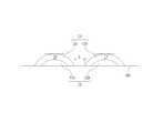
도 1은 본 발명과 관련된 센서의 일 실시 예에 관한 정면도이다.
도 2는 도 1의 센서의 분해 사시도이다.
도 3은 도 1의 A-A' 영역 단면도이다.
도 4은 도 1의 A-A' 영역 단면 일부 확대도이다.
도 5는 본 발명의 센서가 외부 기기와 연동하는 일 실시 예에 관한 것이다.
도 6는 회로 배선, 센싱 전극, 코팅 전극 및 패시베이션 레이어의 구조를 보인 개념도이다.
도 7은 본 발명과 관련된 센서의 제조 방법에 관한 흐름도이다.
도 8은 본 발명과 관련된 센서의 또 다른 제조 방법에 관한 흐름도이다.
도 9(a) 및 도 9(b)는 종래의 센서와 본 발명과 관련된 센서 각각에 대한 측정 횟수에 따른 ADC 변화를 측정한 그래프를 도시한 것이다.1 is a front view of an embodiment of a sensor according to the present invention.
2 is an exploded perspective view of the sensor of FIG. 1.
3 is a cross-sectional view taken along the line AA ′ of FIG. 1.
4 is an enlarged view of a portion of the AA ′ region in FIG. 1.
5 is a view illustrating an embodiment in which a sensor of the present invention works with an external device.
6 is a conceptual diagram illustrating a structure of a circuit wiring, a sensing electrode, a coating electrode, and a passivation layer.
7 is a flowchart illustrating a method of manufacturing a sensor according to the present invention.
8 is a flow chart related to another method of manufacturing a sensor according to the present invention.
9 (a) and 9 (b) show a graph of measuring the change in ADC according to the number of measurements for each of the conventional sensor and the sensor related to the present invention.
도 1은 본 발명과 관련된 센서(100)의 일 실시 예에 관한 정면도이고, 도 2는 도 1의 센서(100)의 분해 사시도이다. 설명의 편의를 위해 도 1 및 도 2를 함께 참조한다.1 is a front view of an embodiment of a
센서(100)는 크게 기판(110), 전도성 레이어(120) 및 절연층으로 구성될 수 있다. 이때 전도성 레이어(120)는 안테나 패턴(121), 센싱 전극(122) 및 회로 배선(124)을 포함할 수 있다.The
기판(110)은 비전도성의 레이어를 구성한다. 기판(110)은 전도성 레이어(120)가 실장되는 상대물 역할을 수행한다. 일 예로, 기판(110)은 플라스틱 레이어(111)와 실리카 레이어(112)를 포함할 수 있다.
플라스틱 레이어(111)는 연성을 갖는 플라스틱(고분자화합물 또는 합성수지)으로 이루어진다. 플라스틱은 폴리에틸렌 테리프탈레이트(polyethylene erephthalate, PET), 폴리이미드(polyimide, PI), 폴리스타이렌(polystyrene, PS) 및 폴리에틸렌 나프탈레이트(polyethylene naphthalate, PEN)로 이루어진 군으로부터 선택된 적어도 하나를 포함할 수 있다.The
실리카 레이어(112)는 플라스틱 레이어(111)의 일면에 코팅될 수 있다. 실리카 레이어(112)는 플라스틱 레이어(111)와 전도성 레이어(120)의 사이에 형성될 수 있다. 실리카 레이어(112)는 센싱 대상 물질(10), 특히 용액의 빠른 퍼짐, 센싱 대상 물질(10)의 안정화, 전도성 레이어(120)의 부착 강도 강화를 가능하게 한다. 실리카 레이어(112)는 수~수십nm의 두께를 가질 수 있다.The
전도성 레이어(120)는 기판(110)의 일면에 구비될 수 있다.The
전도성 레이어(120)는 전술한 바와 같이 안테나 패턴(121), 회로 배선(124) 및 센싱 전극(122)을 포함할 수 있다.As described above, the
센싱 전극(122)은 센싱 대상 물질(10)의 접촉에 의해 임피던스 변화를 일으킨다. 임피던스 변화는 센싱 대상 물질(10)의 상태를 의미할 수 있다.The
센싱 전극(122)의 구체적인 특징들은 후술하도록 한다.Specific features of the
안테나 패턴(121)은 외부 기기와 무선 신호를 송수신한다. 예를 들어, 외부 기기의 센싱 명령 신호를 수신하여 센싱 대상 물질(10)의 임피던스 변화를 측정하거나, 측정된 임피던스 변화 값을 외부 기기로 송신하는 기능을 수행할 수 있다.The
회로 배선(124)은 안테나 패턴(121)과 센싱 전극(122)을 전기적으로 연결하여 신호를 전달하는 통로를 형성한다.The circuit wiring 124 electrically connects the
전도성 레이어(120)는 일체로 형성될 수 있다. 전도성 레이어(120)의 안테나 패턴(121), 센싱 전극(122) 및 회로 배선(124)이 일체로 형성된다는 의미는 기능적으로 상호 구분될 뿐, 구조적으로 동일한 물질, 제조 공정의 측면에서 동일한 공정에 의해 형성될 수 있음을 의미할 수 있다. 다만, 경우에 따라 전도성 레이어(120) 중 코팅 전극(123)은 다른 구성과 달리 이형 물질 또는 구분되는 공정으로 구현될 수 있다. 자세한 사항은 후술한다.The
또는 필요에 따라 전도성 레이어(120)는 일체로 형성되지 않고 별도의 공정에 의해 각각 따로 형성될 수 있다.Alternatively, if necessary, the
일체로 구비된 전도성 레이어(120)는 원칙상 물리적으로 분리되지 않을 수 있다.The
전도성 레이어(120)는 기판(110)에 전자 인쇄 방식으로 형성될 수 있다.The
종래에는 전도성 레이어(120)가 진공 증착법에 의해 형성되었다. 진공 증착법에 의한 전도성 레이어(120)의 형성은 안정적인 구조를 가지는 장점이 있으나, 진공 증착 이후 에칭 등의 추가 공정을 거쳐야 한다는 점에서 제조 및 재료 비용이 많이 요구되며, 고온에서 이루어지므로 기판(110)의 형태 변형 등을 가져올 수 있다.Conventionally, the
전도성 레이어(120)의 전자 인쇄 공정은 그라비어 오프셋(Gravure offset), 그라비어 인쇄(Gravure printing) 또는 스크린 인쇄(Screen printing) 중 어느 하나의 방식으로 행해질 수 있다.The electronic printing process of the
전도성 레이어(120)의 적어도 일부는 동일한 레이어로 형성될 수 있다. 전도성 레이어(120)의 적어도 일부가 동일한 물질 및 동일한 레이어로 형성된다는 것은 제조 공정의 측면에서 1회의 인쇄 공정에 의해 기판(110)에 인쇄되는 것을 의미할 수 있다. 1회의 인쇄 공정에 의해 구비되는 경우 제조 공정의 단순화를 가져올 수 있어 제조 비용 및 시간을 최소화 할 수 있다.At least a portion of the
구체적으로, 동일한 레이어로 형성되는 전도성 레이어(120)의 영역은, 안테나 패턴(121)의 전부 또는 일부, 그리고 회로 배선(124), 그리고 센싱 전극(122)을 포함할 수 있다. 자세한 내용은 후술하도록 한다.In detail, the region of the
안테나 패턴(121)은 외부 기기와 신호를 송수신한다.The
외부 기기란 통신 기능을 가진 전자 기기를 의미할 수 있다. 예를 들어, 스마트폰, 컴퓨터, 디지털 방송용 단말기, PDA 등이 있다.The external device may mean an electronic device having a communication function. For example, there are a smartphone, a computer, a digital broadcasting terminal, a PDA, and the like.
안테나 패턴(121)은 외부 기기로부터 무선 신호를 수신하여 직류 전원을 생성하고, 생성된 직류 전원은 센서(100)의 측정 구동에 이용된다. 측정된 센싱 대상 물질(10)의 임피던스 차이는 다시 안테나 패턴(121)을 통해 외부 기기로 송신될 수 있다.The
안테나 패턴(121)에 의해 직류 전원이 생성되므로 센서(100)에는 별도의 전원 공급부가 구비되지 않을 수 있다. 이는 센서(100)의 경박단소 및 제조 비용의 최소화를 가져올 수 있다.Since DC power is generated by the
안테나 패턴(121)은 기판(110)의 일면에 2차원으로 형성될 수 있다. 특히, 안테나 길이를 확보하기 위해 기판(110)의 외측 모서리를 따라 구비되고, 필요한 길이에 따라 복수회 감겨 나선형으로 구비될 수 있다. 안테나 패턴(121)의 형상 및 패턴은 안테나의 기능 구현을 위해 다양하게 변경될 수 있다.The
안테나 패턴(121)은 높은 인덕턴스를 갖기 위해 500~1500㎛의 선폭을 가질 수 있다. 복수회 감긴 안테나 패턴(121)의 인접한 라인간의 간격은 300~700㎛을 가져 적절한 커패시턴스 성분을 갖도록 할 수 있다.The
안테나 패턴(121)은 안테나 본연의 기능을 수행하기 위한 패턴 영역과, 패턴 영역과 회로 배선(124) 또는 센싱 전극(122)과 전기적으로 연결하기 위한 연결 영역을 포함할 수 있다. 패턴 영역 및 연결 영역은 동일한 레이어에 구비될 수도 있으나, 다른 구성과의 전기적 연결을 원활하게 수행하기 위해 서로 다른 레이어에 구비될 수도 있다. 이를 위해 서로 다른 레이어 간의 의도하지 않은 전기적 연결을 방지하기 위해 절연 영역이 추가적으로 구비될 수 있다. 자세한 내용은 후술하도록 한다.The
안테나 패턴(121)은 NFC(Near Field Communication) 안테나의 방사체로 작동할 수 있다. NFC 안테나는 13.56MHz의 통신 규격을 이용하여 정보의 교환이 이루어질 수 있다.The
회로 배선(124)은 안테나 패턴(121)과 센싱 전극(122)을 전기적으로 연결한다. 또 회로 배선(124)은 센서(100)를 제어하는 소자(150)와 전기적으로 연결할 수 있다. 즉, 회로 배선(124)은 전도성 레이어(120) 중 안테나 패턴(121)과 센싱 전극(122)을 제외한 모든 영역을 의미할 수 있다.The circuit wiring 124 electrically connects the
패시베이션 레이어(131)는 센싱 대상 물질(10)이 기판(110) 영역으로 누설되는 것을 방지한다. 따라서 센싱 대상 물질(10)이 회로 배선(124) 등으로 흘러 센서(100)가 오작동을 일으키는 것을 방지한다. 또한 패시베이션 레이어(131)는 일정한 높이를 가져 센싱 대상 물질(10)의 유동을 방지할 수도 있다. 센싱 대상 물질(10)을 센싱 전극(122)으로 모을 수 있다.The
패시베이션 레이어(131)는 표면 에너지가 기판(110)보다 커서 센싱 대상 물질(10)이 패시베이션 레이어(131) 영역 내에 액정을 형성하여 기판(110)으로 퍼지지 않도록 할 수 있다.The
패시베이션 레이어(131)는 센싱 전극(122)의 적어도 일 영역을 노출시키는 제1 개구부(131a)를 구비할 수 있다. 센싱 전극(122)은 제1 개구부(131a)를 통해 노출된 일부 영역만 사용될 수 있다.The
센싱 전극(122)의 전체 길이 A는 400~5000㎛ 이고, 제1 개구부(131a)를 통해 노출되는 길이는 50~5000㎛가 될 수 있다. 경우에 따라 센싱 전극(122)의 전체 길이와 제1 개구부(131a)를 통해 노출되는 길이는 동일할 수도 있고, 또는 센싱 전극(122)의 일부만 제1 개구부(131a)를 통해 노출될 수도 있다.The total length A of the
제1 개구부(131a)를 통해 노출되는 센싱 전극(122)의 노출 길이는 센서(100)의 분해능과, 대량 생산에 따른 인쇄 재현성, 센서(100)의 신뢰성에 영향을 미친다. 제1 개구부(131a)를 통해 노출되는 센싱 전극(122)의 노출 길이가 짧을수록 센서(100)의 분해능은 향상될 수 있다.The exposure length of the
센싱 전극(122)의 폭 B는 50~1000㎛ 범위 내에서 구비될 수 있다. 센싱 전극(122)의 폭 B가 좁을수록 센서(100)의 분해능이 향상될 수 있다. 그러나 지나치게 좁은 센싱 전극(122)의 폭은 전도성 레이어(120)의 인쇄 공정을 불안정하게 만들 수 있다. 안정적인 인쇄 공정을 위해 센싱 전극(122)의 폭 B는 50~200㎛인 것이 바람직하다.Width B of the
센싱 전극(122)의 양 극 각각을 제1 센싱 전극(122a) 및 제2 센싱 전극(122b)이라 할 때, 제1 센싱 전극(122a)과 제2 센싱 전극(122b) 사이의 간격 C는 50~3000㎛ 범위 내에서 구비될 수 있다.When each positive electrode of the
다만 제1 센싱 전극(122a)과 제2 센싱 전극(122b) 사이의 간격 C가 만약 지나치게 멀고, 센싱 대상 물질의 양이 충분하지 않은 경우에는 정확한 측정이 어려울 수 있다. 즉, 센싱 대상 물질은 액적을 형성하여 제1 센싱 전극(122a)과 제2 센싱 전극(122b)에 모두 접촉해야 한다. 이 점을 고려하여 제1 센싱 전극(122a)와 제2 센싱 전극(122b) 사이의 간격 C는 900~1500㎛ 범위 내에서 구비되는 것이 바람직하다.However, if the distance C between the
센싱 전극(122)의 높이 D는 700nm~15㎛가 될 수 있다. 센싱 전극(122)의 높이 D는 센서(100)의 두께와 센싱 전극(122)의 내구성과 신뢰성에 영향을 줄 수 있다. 센싱 전극(122)의 높이 D가 700nm보다 낮으면 센싱의 반복에 따라 센싱 전극(122)의 소실 문제가 발생할 수 있다. 인쇄 공정의 한계 및 센서(100)의 두께 증가를 방지하기 위해, 센싱 전극(122)의 높이는 15㎛보다 낮은 것이 바람직하다.The height D of the
안테나 절연층(132) 및 안테나 브릿지(140)는 안테나 패턴(121)이 회로 배선(124)과 연결되기 위한 구조를 형성한다. 안테나 패턴(121)이 기판(110)에 복수회 감겨 나선형으로 형성되는 경우 부득이 하게 안테나 패턴(121)의 일단은 안테나 패턴(121)의 타단이 구비된 방향으로 연장되어야 한다. 안테나 브릿지(140)는 이러한 연장 영역을 형성하고, 안테나 브릿지(140)와 기존 인쇄 공정을 통해 인쇄된 안테나 패턴(121)이 서로 간섭하지 않도록 안테나 절연층(132)이 안테나 브릿지(140)와 안테나 패턴(121) 사이에 구비될 수 있다.The
보호 레이어(160)는 절연 소재로 형성되어 기판(110)의 일면을 마주보도록 배치되어 기판(110), 전도성 레이어(120) 및 패시베이션 레이어(131) 등 기판(110)에 실장된 모든 구성들을 덮어 해당 구성들을 전기적, 물리적으로 보호하는 역할을 수행할 수 있다. 다만 보호 레이어(160)는 패시베이션 레이어(131)의 제1 개구부(131a)를 노출시키는 제2 개구부(160a)를 구비할 수 있다.The
소자(150)는 기판(110)에 실장되어 회로 배선(124)과 전기적으로 연결될 수 있다.The
센서(100)의 작동과 관련된 각종 전자적 구성들은 소자(150)에 의해 구현될 수 있다. 전자적 구성은 예를 들어 전원생성부, 제어부, 변환부, 통신부 등을 포함할 수 있다.Various electronic components related to the operation of the
안테나 패턴(121)을 통해 수신된 무선 신호는 회로 배선(124)을 통해 소자(150)로 전달된다. 소자(150)는 공급 받은 직류 전원을 교류 전원으로 생성하여 센싱 전극(122)에 입력할 수 있다.The wireless signal received through the
도 3은 도 1의 A-A' 영역 단면도이고, 도 4은 도 1의 A-A' 영역 단면 일부 확대도이다. 설명의 편의상 도 3 및 도 4를 함께 참조한다.3 is a cross-sectional view taken along the line AA ′ of FIG. 1, and FIG. 4 is an enlarged view of a portion of the cross section along the line AA ′ of FIG. 1. For convenience of description, reference is made to FIGS. 3 and 4 together.
센싱 전극(122)은 센싱 대상 물질(10)이 직접적으로 접하는 것으로, 진공 증착 방식을 통해 형성되는 경우 센싱 전극(122) 영역 만을 백금(Pt)이나 금(Au)과 같은 물질을 사용하면 족하다. 하지만 상술한 바와 같이 전자 인쇄 방식을 통해 안테나 패턴 및 회로 배선 등을 동일 레이어로 구성하는 경우에는 재료 비용이 과도하게 증가한다.The
이러한 문제점은 센싱 전극(122)을 은(Ag), 구리(Cu) 및 알루미늄(Al) 등과 같은 물질로 대체함으로써 해결할 수 있다.This problem may be solved by replacing the
즉, 은, 구리 및 알루미늄은 센싱 전극(122) 중 센싱 전극(122)의 주요 구성으로 구비될 수 있다.That is, silver, copper, and aluminum may be provided as main components of the
센싱 전극(122)은 은, 구리 및 알루미늄과 같은 전도성 입자(1221)와 유기물로 구성된 바인더(Binder, 1222)의 결합 구성으로 이루어질 수 있다. 전도성 입자(1221)는 구형 또는 플레이크(flake, 편상)의 형상을 가질 수 있다. 플레이크 형상의 전도성 입자(1221)는 구형인 경우에 비해 상대적으로 높은 전도도를 가질 수 있다.The
전도성 입자(1221)는 반응 비표면적 확보를 위해 수십nm~20㎛의 크기를 가질 수 있다. 센싱 전극(122)은 센싱 대상 물질(10)과 반응하여 임피던스 변화를 일으키는데, 임피던스에는 커패시턴스(capacitance) 성분과 저항 성분이 존재한다. 전도성 입자(1221)의 반응 비표면적이 넓으면 커패시턴스 성분도 커진다. 전도성 입자(1221)의 반응 비표면적이 넓으면 반응에 의한 센싱 전극(122)의 산화 또는 부식이 억제될 수 있으며, 센서(100)의 수명이 연장될 수 있다.The
바인더(1222)는 전도성 입자(1221)를 지지한다. 바인더(1222)는 센싱 전극(122)의 내구성 및 신뢰성을 향상시키는 역할을 할 수 있다.The
바인더(1222)는 폴리에틸렌 옥사이드(Polyethylene oxide, PEO) 계열, 올레산(Oleic acid) 계열, 아크릴레이트(Acrylate) 계열, 아세테이트(Acetate) 계열 및 에폭시(Epoxy) 계열로 이루어진 군으로부터 선택된 적어도 하나의 수지(resin)를 포함할 수 있다.The
센싱 전극(121)은 기공(1213)을 가질 수 있다. 기공(1213)은 수nm-수십㎛의 크기를 가질 수 있다. 센싱 전극(121)이 기공(1213)을 가지면, 반복적인 기계적 변형에 의해 쉽게 파손되지 않으므로 센서(100)의 신뢰성을 향상시킬 수 있다.The
센싱 전극(122)은 기판(110)과 예각을 형성할 수 있다. 즉, 센싱 전극(122)의 가장자리 영역은 기판(110)으로부터 완만한 경사를 이루어 기판(110)의 휘어짐 등에 의해 센싱 전극(122)이 쉽게 박리되지 않도록 한다.The
다만, 센싱 전극(122)이 그대로 노출되어 센싱 대상 물질(10)과 접촉하는 경우 은, 구리 및 알루미늄과 같은 물질의 표준 환원 전위가 낮아 부식 우려가 있다. 센싱 전극(122)의 부식은 센싱 대상 물질(10)과 센싱 전극(122)의 접촉을 방해하여 임피던스 측정의 노이즈 발생 원인이 된다.However, when the
또한 센싱 전극(122)의 입자 크기들로 인해 센싱 대상 물질(10)과 닿는 표면적이 작아지게 되고, 이러한 접촉 표면적의 감소 또한 센싱의 정확도를 감소시키는 요인이 된다.In addition, due to the particle sizes of the
상기 센싱 전극(122)의 구성으로 인한 전도성 향상, 전도성 센싱의 신뢰도 및 내구성 강화를 위한 세 가지 실시 예 방안을 후술하도록 한다.Three embodiments of the present invention for improving conductivity, enhancing reliability of conductive sensing, and durability due to the configuration of the
- 실시 예 1 -Example 1
센싱 전극(122)의 외측에 코팅 전극(123)을 구비할 수 있다.The
코팅 전극(123)은 전자 인쇄 방식을 통해 센싱 전극(122)의 외측면에 추가적으로 구비되어 센싱 전극(122)에 민감화 처리를 할 수 있다.The
코팅 전극(123)으로 인해 센싱 전극(122)이 센싱하는 임피던스 변화의 노이즈 발생 가능성이 감소한다. 즉, 코팅 전극(123)은 센싱 대상 물질(10)과 센싱 전극(122)이 전기 전도도를 상승시키는 역할을 한다.The
나아가, 센싱 전극(122)의 내구성 및 내마모성을 높일 수 있다.In addition, durability and wear resistance of the
코팅 전극(123)은 센싱 전극(122)과 유사한 구성으로 이루어질 수 있다. 즉, 전도성 입자(1231)와 바인더(1232)의 결합 구성으로 구비될 수 있다.The
코팅 전극(123)의 전도성 입자(1231)는 탄소 나노 튜브(CNT)를 포함할 수 있다.The
코팅 전극(123)의 바인더(1232)는 코팅 전극(123)의 전도성 입자(1231)를 연결시켜 공극(1233)이 형성되는 것을 최소화 할 수 있다. 코팅 전극(123)의 바인더는 센싱 전극(122)의 바인더(1222)와 마찬가지로 폴리에틸렌 옥사이드(Polyethylene oxide) 계열, 올레산(Oleic acid) 계열, 아크릴레이트(Acrylate) 계열, 아세테이트(Acetate) 계열 및 에폭시(Epoxy) 계열로 이루어진 군으로부터 선택된 적어도 하나의 수지(resin)를 포함할 수 있다.The
다만, 코팅 전극(123)의 전도성 입자(1231)가 탄소 나노 튜브만으로 구비되는 경우, 저항이 높아 센싱 분해능이 떨어지기 때문에, 코팅 전극(123)의 전도성 입자(1231)는 추가적으로 그라파이트(Graphite)도 포함할 수 있다. 그라파이트는 센싱 전극(122)의 전도성을 높이는 역할을 한다.However, when the
또한, 코팅 전극(123)의 전도성 입자(1231)는 카본 블랙(Carbon black)을 포함할 수도 있다. 카본 블랙은 센싱 전극(122)의 내구성 또는 내마모성을 강화시키는 역할을 한다.In addition, the
그라파이트 및 카본 블랙은 코팅 전극(123)의 전도 물질 총 질량의 10% 이상으로 구성될 수 있다.Graphite and carbon black may consist of at least 10% of the total mass of the conductive material of the
전도성 입자(1231)의 탄소 나노 튜브, 그라파이트 및 카본 블랙은 독립적으로 각 기능을 수행하는 것이 아니라 상호 유기적으로 연계하여 상기 기능들을 수행하게 된다.The carbon nanotubes, graphite, and carbon black of the
코팅 전극(123)은 센싱 전극(122)의 외측면을 덮는 형태로 구비될 수 있다. 센싱 전극(122)의 기공(1223)은 상술한 바와 같이 센서(100)의 기계적 변형에 대한 내구성을 갖도록 하는 역할을 하지만, 반대로 센싱 전극(122)의 전도도를 낮춰 정확한 임피던스 측정을 방해한다. 코팅 전극(123)의 구비는 이러한 센싱 전극(122)의 기공(1223)을 채워 높은 전도도를 갖도록 하여 정확한 임피던스 측정이 가능하도록 한다.The
전술한 바와 같이 센싱 전극(122)은 센싱 대상 물질(10)과 접촉하기 위해 이격된 두 전극(122a, 122b)을 가지고, 이는 코팅 전극(123)에도 동일하게 적용된다.As described above, the
코팅 전극(123)의 이격된 두 전극 제1 코팅 전극(123a) 및 제2 코팅 전극(123b)의 간격은 10㎛ 이격될 수 있다. 이 수치는 대략적인 값에 해당할 뿐, 정확하게 10㎛일 것을 요구하는 것은 아니다.Two electrodes spaced apart from the
그리고 코팅 전극(123)의 두께, 즉 센싱 전극(122)의 최상단으로부터 코팅 전극(123)의 최상단까지의 두께는 10㎛ 이하가 될 수 있다.The thickness of the
코팅 전극(123)의 외측에는 상술한 패시베이션 레이어(131)가 구비될 수 있다. 즉, 기판(110)으로부터 외측으로 센싱 전극(122), 코팅 전극(123) 및 패시베이션 레이어(131)가 차례대로 적층되어 구비될 수 있다. 따라서 코팅 전극(123)의 길이 조건은 상술한 센싱 전극(122)의 길이 조건 등과 동일하게 적용될 수 있다. 따라서 코팅 전극(123)은 센싱 전극(122)과 동일한 길이만큼 제1 개구부(131a)를 통해 외부로 노출될 수 있다.The
- 실시 예 2 -Example 2
센싱 전극(122)의 전도성 향상을 위해, 상술한 코팅 전극과 달리 공액 고분자층이 사용될 수도 있다. 공액 고분자층은 전도성 폴리머(PEDOT:PSS/P3HT)와 같은 물질로 구성될 수 있다. 공액 고분자층은 센싱 전극(122)에 패터닝 공정으로 구현될 수도 있고, 또는 전면만 코팅된 상태에서 센싱 전극(122)에 일정 시간 흡수되도록 경과한 후 제거하는 공정을 거칠 수도 있다.In order to improve conductivity of the
- 실시 예 3 -Example 3
센싱 전극(122)의 전도성을 향상시키고 측정 신뢰도를 유지하기 위해, 센싱 전극(122)은 롤링 공정을 통해 압착될 수 있다. 센싱 전극(122)이 인쇄된 상태에서, 일정 온도를 상승시키고, 상승된 온도가 유지되는 상태에서 롤러를 통해 센싱 전극(122)을 압착할 수 있다.In order to improve conductivity of the
다만, 롤링 공정을 통해 센싱 전극(122)이 압착되는 경우, 압력에 의해 센싱 전극(122)의 결합이 깨질 수 있다. 이러한 현상을 최소화 하기 위해, 롤러에 홈을 형성하여 롤링 공정을 수행할 수도 있다.However, when the
도 5는 본 발명의 센서(200)가 외부 기기(20)와 연동하는 일 실시 예에 관한 것이다.5 is a view illustrating an embodiment in which the
이하에서는 별도의 언급이 없는 한 실시 예 1의 센서 형태를 전제로 기술한다. 다만, 모순되지 않는 범위 내에서 실시 예 2 및 3의 경우도 동일하게 적용될 수 있다.Hereinafter, unless otherwise stated, descriptions will be made on the assumption that the sensor form of the first embodiment is described. However, the same may be applied to the case of Examples 2 and 3 within a range that does not contradict.
외부 기기(20)는 여러 형태가 될 수 있으나 이동 단말기, 특히 스마트폰인 것을 일 예로 설명한다.The
센서(200)는 안테나 패턴(221)을 통해 외부 기기(20)와 무선 신호를 수신한다.The
센서(200)는 회로부(250)를 구동하기 위해 전원생성부(251)를 통해 직류 전원을 생성한다. 이와 같이 본 발명의 센서(200)는 스스로 전력 공급을 위한 구성을 갖는 것이 아니라, 외부 기기(20)로부터 수신된 무선 신호를 이용하여 직류 전원을 생성하며, 생성된 직류 전원에 의해 제어부(252), 변환부(253), 통신부(254) 및 센싱 전극(222)이 작동하게 된다.The
제어부(252)는 직류 전원을 공급받아 구동된다. 제어부(252)는 교류 전압을 생성하여 센싱 전극(222)에 입력한다. 실시 예 1의 경우를 전제로, 센싱 전극(222)은 코팅 전극(123, 도 3 참조)까지 포함하는 개념을 지칭할 수 있다. 후술하는 센싱 전극(222)은 코팅 전극을 포함할 수 있다.The controller 252 is driven by receiving DC power. The controller 252 generates an AC voltage and inputs it to the
센싱 전극(222)과 센싱 대상 물질이 반응하게 되면, 센싱 전극(222)은 임피던스 변화를 일으키게 된다. 센싱 전극(222)의 임피던스 변화는 제어부(252)에서 생성한 교류 전압의 변화로 나타나게 된다. 출력 값의 범위에 따라 센싱 대상 물질을 구분할 수도 있다.When the
교류 전압의 변화는 디지털 신호로 변환될 수 있다. 변환부(252)는 센싱 전극(222)의 임피던스 변화에 근거하여 나타나는 교류 전압의 변화를 디지털 신호로 변환한다. 그리고 통신부(254)는 디지털화 된 신호를 안테나 패턴을 통해 외부 기기(20)로 송신한다. 여기서 통신부(254)는 NFC Tag IC가 될 수 있다.The change in AC voltage can be converted into a digital signal. The converter 252 converts a change in AC voltage, which is displayed based on a change in impedance of the
외부 기기(20)는 센서(200)로부터 디지털화된 신호를 전송받아 정보를 생성하고 저장 및 관리하게 된다.The
외부 기기(20)는 디스플레이를 통해 정보를 표시할 수도 있다.The
도 6는 회로 배선(324), 센싱 전극(322), 코팅 전극(323) 및 패시베이션 레이어(331)의 구조를 보인 개념도이다.6 is a conceptual diagram illustrating a structure of a
센서는 인쇄, 열건조 및 경화 과정에 의해 형성된다. 특히, 인쇄 공정을 반복하는 경우 공정 오차, 특히 alignment 오차가 발생할 수 있으며, 열건조 과정에서도 기판의 수축으로 인해 오차가 발생할 수 있다.Sensors are formed by printing, heat drying and curing processes. In particular, when the printing process is repeated, a process error, in particular, an alignment error may occur, and an error may occur due to shrinkage of the substrate even in a heat drying process.
센서의 분해능은 제1 및 제2 센싱 전극(322a, 322b)의 노출 길이에 따라 결정될 수 있다. 제1 및 제2 센싱 전극(322a, 322b)의 전체 길이와 노출 길이는 5,000㎛ 이하로 매우 작아 공정 오차의 발생 확률이 크다. 따라서 공정 오차를 최소화 할 수 있는 구조를 가지는 것이 필요하다.The resolution of the sensor may be determined according to the exposure lengths of the first and
제1 센싱 전극(322a), 제2 센싱 전극(322b), 제1 코팅 전극(323a), 제2 코팅 전극(323b), 회로 배선(324) 및 패시베이션 레이어(331)는 모두 인쇄 공정에 의해 형성될 수 있다. 패시베이션 레이어(331)는 제1 센싱 전극(322a), 제2 센싱 전극(322b), 제1 코팅 전극(323a), 제2 코팅 전극(323b) 및 회로 배선(324)을 덮도록 배치된다. 따라서 패시베이션 레이어(331)는 센싱 전극(322a, 322b), 코팅 전극(323a, 323b) 및 회로 배선(324)의 인쇄 후에 형성된다. 따라서 인쇄 공정의 반복과 열건조 과정에서 공정 오차가 발생할 수 있으며, 따라서 센싱 전극(322a, 322b) 또는 코팅 전극(323a, 323b)이 설계 의도와 달리 노출되거나 가려질 수 있다.The
센싱 전극(322a, 322b) 및 코팅 전극(323a, 323b)은 길이 방향을 따라 세 부분으로 구분될 수 있다. 이를 제1 단부(322a1, 322b1, 323a1, 323b1), 제2 단부(322a2, 322b2, 323a2, 323b2) 및 중앙부(322a3, 322b3, 323a3, 323b3)로 정의한다. 패시베이션 레이어(331)는 제1 단부(322a1, 322b1, 323a1, 323b1)와 제2 단부(322a2, 322b2, 323a2, 323b2)를 덮고, 제1 개구부(331a)는 중앙부(322a3, 322b3, 323a3, 323b3)를 노출시킨다.The
센싱 전극(322) 및 코팅 전극(323)은 제1 개구부(331a)의 길이보다 길게 형성된다. 제1 개구부(331a)는 센싱 전극(322) 및 코팅 전극(323)의 노출 길이를 제어할 수 있다. 따라서 패시베이션 레이어(331)의 제1 개구부(331a)의 길이 G를 정밀하게 조절함으로써 오차를 낮출 수 있다.The sensing electrode 322 and the coating electrode 323 are formed longer than the length of the
제1 개구부(331a)의 폭 H는 센싱 전극(322) 또는 코팅 전극(323)의 제1 전극(322a, 323a) 및 제2 전극(322b, 323b)의 사이 간격 보다는 넓고, 5000㎛을 넘지 않는 것이 바람직하다. 제1 개구부(331a)의 폭 H가 지나치게 넓으면 센싱 전극(322) 또는 코팅 전극(323)에 접촉하게 될 대상 센싱 물질이 액적을 형성하지 않고 퍼질 수 있기 때문이다.The width H of the
실험 결과를 통해 제1 개구부(331)를 통해 노출되는 센싱 전극(322) 또는 코팅 전극(323)의 길이가 짧을수록, 센싱 전극(322) 또는 코팅 전극(323)의 폭이 좁을수록, 두 전극 사이의 간격이 넓을수록 분해능은 향상된다. 그러나, 오직 분해능 향상만을 목적으로 센싱 전극(322) 및 코팅 전극(323)을 설계하게 되면, 내구성 및 신뢰성 등의 문제가 발생할 수 있다. 따라서 분해능, 내구성 및 신뢰성 등을 고려하여 센싱 전극(322) 및 코팅 전극(323)의 구조가 설계되어야 한다.The shorter the length of the sensing electrode 322 or the coating electrode 323 exposed through the first opening 331, the narrower the width of the sensing electrode 322 or the coating electrode 323, the two electrodes The wider the interval, the better the resolution. However, when the sensing electrode 322 and the coating electrode 323 are designed only for the purpose of improving resolution, problems such as durability and reliability may occur. Therefore, the structures of the sensing electrode 322 and the coating electrode 323 should be designed in consideration of resolution, durability, and reliability.
도 7 및 도 8은 본 발명과 관련된 센서의 제조 방법에 관한 흐름도이다.7 and 8 are flowcharts illustrating a manufacturing method of a sensor according to the present invention.
도 7을 참조하면, 전도성 레이어는 인쇄 공정을 통해 기판에 인쇄된다(S100). 전도성 레이어는 안테나 패턴, 센싱 전극, 코팅 전극 및 회로 배선을 포함한다.Referring to FIG. 7, the conductive layer is printed on the substrate through a printing process (S100). The conductive layer includes an antenna pattern, sensing electrode, coated electrode and circuit wiring.
안테나 패턴, 센싱 전극 및 회로 배선을 동일 물질로 구성하는 경우, 한 번의 인쇄 공정에 의해 전도성 레이어 중 안테나 패턴, 센싱 전극 및 회로 배선이 동시에 형성될 수 있다(S110). 따라서 이는 재료 및 제조 비용의 절감을 가져올 수 있다. 이를 편의상 제1 인쇄 공정으로 정의한다. 제1 인쇄 공정으로 인해 안테나 패턴, 센싱 전극 및 회로 배선은 동일한 레이어에 구비될 수 있다.When the antenna pattern, the sensing electrode, and the circuit wiring are made of the same material, the antenna pattern, the sensing electrode, and the circuit wiring among the conductive layers may be simultaneously formed by one printing process (S110). This can therefore result in a reduction of material and manufacturing costs. This is defined as a first printing process for convenience. Due to the first printing process, the antenna pattern, the sensing electrode, and the circuit wiring may be provided on the same layer.
이후 센싱 전극의 외측면에 코팅 전극이 인쇄될 수 있다(S120). 코팅 전극은 센싱 전극과 다른 물질로 구성되므로 추가적인 제2 인쇄 공정을 통해 형성될 수 있다.Thereafter, the coating electrode may be printed on the outer surface of the sensing electrode (S120). Since the coating electrode is made of a material different from the sensing electrode, it may be formed through an additional second printing process.
따라서 코팅 전극은 센싱 전극이 구비되는 레이어의 상단에 적층된 이형 레이어를 구성하게 된다.Therefore, the coating electrode constitutes a release layer stacked on top of the layer on which the sensing electrode is provided.
전도성 레이어의 인쇄 공정은 분말 잉크 또는 페이스트를 이용한다. 분말 잉크 또는 페이스트의 조성은 전도성 입자 40~70 중량%, 용매를 포함하는 유기물 30~60 중량%로 이루어질 수 있다. 이를 통해 센싱 전극 또는 코팅 전극의 산화 및 부식을 최소화 할 수 있다.The printing process of the conductive layer uses powder ink or paste. The composition of the powder ink or paste may be 40 to 70 wt% of the conductive particles and 30 to 60 wt% of the organic material including a solvent. This can minimize oxidation and corrosion of the sensing electrode or coating electrode.
전술한 바와 같이, 센싱 전극의 전도성 입자는 은(Ag), 구리(Cu) 및 알루미늄(Al) 중 적어도 하나로 이루어질 수 있다. 한편 코팅 전극의 전도성 입자는 탄소 나노 튜브(CNT), 그라파이트(Graphite) 및 카본 블랙(Carbon black) 중 적어도 하나로 이루어질 수 있다.As described above, the conductive particles of the sensing electrode may be made of at least one of silver (Ag), copper (Cu), and aluminum (Al). Meanwhile, the conductive particles of the coating electrode may be made of at least one of carbon nanotubes (CNT), graphite, and carbon black.
센싱 전극의 전도성 입자 또는 코팅 전극의 전도성 입자는 구형 또는 플레이크(flake) 형상을 가질 수 있다.The conductive particles of the sensing electrode or the conductive particles of the coating electrode may have a spherical or flake shape.
전도성 입자 및 바인더를 섞는 용매는 아세톤(Acetone), 알릴알코올(Allyl alcohol), 아세트산(Acetic acid), 아세톨(Acetol), 메틸알코올(Methyalcohol) 및 벤젠(Benzene)으로 이루어진 군으로부터 선택된 적어도 하나를 포함할 수 있다.The solvent for mixing the conductive particles and the binder is at least one selected from the group consisting of acetone, allyl alcohol, acetic acid, acetol, methyl alcohol and benzene. It may include.
전도성 레이어를 인쇄하는 공정은 스크린(Screen), 오프셋(Offset), 그라비어(Gravure) 중 어느 하나가 될 수 있다.The process of printing the conductive layer may be any one of a screen, an offset, and gravure.
인쇄 공정 이후 열건조를 통해 전도성 레이어를 경화시킬 수 있다(S200). 열건조는 80~200℃에서 이루어질 수 있다. 열건조 과정에서 상술한 용매는 증발될 수 있다. 200℃ 이하의 저온 공정이 가능하기 위해서는 전도성 입자가 분말 형태로 수십nm~20㎛의 크기를 갖는 것이 바람직하다.After the printing process, the conductive layer may be cured through heat drying (S200). Heat drying may be performed at 80 ~ 200 ℃. The solvent described above may be evaporated in the heat drying process. In order to enable a low temperature process of 200 ° C. or less, it is preferable that the conductive particles have a size of several tens of nm to 20 μm in powder form.
특히, 열건조는 센싱 전극을 인쇄하는 제1 인쇄 공정과 코팅 전극을 인쇄하는 제2 인쇄 공정 이후에 수행될 수 있다. 열건조 이전에 센싱 전극 위에 코팅 전극을 인쇄함으로써 코팅 전극이 센싱 전극의 공극 사이로 유입되어 센싱 전극과 코팅 전극이 좀 더 밀하게 결합될 수 있다. 센싱 전극과 코팅 전극이 밀하게 결합하는 경우 전도도가 높아지며, 높은 결합력에 의해 코팅 전극이 기판 또는 센싱 전극으로부터 쉽게 박리되는 것을 방지할 수 있다.In particular, the heat drying may be performed after the first printing process for printing the sensing electrode and the second printing process for printing the coating electrode. By printing the coating electrode on the sensing electrode prior to heat drying, the coating electrode may be introduced between the pores of the sensing electrode, so that the sensing electrode and the coating electrode may be more tightly coupled. When the sensing electrode and the coating electrode are tightly coupled, the conductivity is increased, and the high bonding force may prevent the coating electrode from being easily peeled off from the substrate or the sensing electrode.
또는 도 8과 같이, 센싱 전극의 제1 인쇄 공정 이후 1차적으로 열건조 공정을 거치고, 이후 코팅 전극에 대한 제2 인쇄 공정을 수행할 수도 있다.Alternatively, as shown in FIG. 8, after the first printing process of the sensing electrode, the heat drying process may be performed first, and then the second printing process may be performed on the coating electrode.
제1 인쇄 공정 및 제2 인쇄 공정 모두에 대한 열건조 공정이 끝난 이후 패시베이션 레이어 및 안테나 절연층을 인쇄할 수 있다(S300).After the heat drying process for both the first printing process and the second printing process is finished, the passivation layer and the antenna insulation layer may be printed (S300).
패시베이션 레이어와 안테나 절연층은 동일한 소재로 이루어질 수 있고, 따라서 하나의 인쇄 공정을 통해 동시에 형성될 수 있다. 즉, 패시베이션 레이어와 안테나 절연층은 전도성 레이어 위에 동일 레이어를 형성할 수 있다.The passivation layer and the antenna insulation layer may be made of the same material, and thus may be simultaneously formed through one printing process. That is, the passivation layer and the antenna insulating layer may form the same layer on the conductive layer.
인쇄된 패시베이션 레이어와 안테나 절연층은 경화 과정을 거칠 수 있다(S400). 패시베이션 레이어와 안테나 절연층의 경화는 자외선(UV)에 의해 될 수 있다.The printed passivation layer and the antenna insulation layer may undergo a curing process (S400). Curing of the passivation layer and antenna insulation layer may be by ultraviolet (UV).
안테나 절연층은 확실한 절연 신뢰도를 보장받기 위해 복수회의 인쇄 공정을 가질 수 있다(S500). 이때 먼저 인쇄된 안테나 절연층을 제1 안테나 절연층, 이후에 인쇄된 안테나 절연층을 제2 안테나 절연층으로 정의할 수 있다. 제2 안테나 절연층의 인쇄 이후 제1 안테나 절연층의 경화 과정과 마찬가지로 경화 과정을 한번 더 거칠 수 있다(S600).The antenna insulation layer may have a plurality of printing processes in order to ensure reliable insulation reliability (S500). In this case, the first printed antenna insulating layer may be defined as the first antenna insulating layer, and the subsequently printed antenna insulating layer may be defined as the second antenna insulating layer. After the printing of the second antenna insulation layer, the curing process may be performed once more as in the curing process of the first antenna insulation layer (S600).
필요에 따라, 제1 안테나 절연층 및 제2 안테나 절연층에 더하여 추가적으로 안테나 절연층이 인쇄될 수 있다. 이 경우 제1 안테나 절연층 또는 제2 안테나 절연층이 형성된 공정과 동일한 경화 과정을 거친다.If necessary, an antenna insulation layer may be additionally printed in addition to the first antenna insulation layer and the second antenna insulation layer. In this case, the same hardening process is performed as the process of forming the first antenna insulation layer or the second antenna insulation layer.
안테나 절연층 위에는 안테나 브릿지가 인쇄된다(S700). 안테나 브릿지는 전도성 레이어와 동일한 소재로 이루어질 수 있다.An antenna bridge is printed on the antenna insulation layer (S700). The antenna bridge may be made of the same material as the conductive layer.
안테나 브릿지는 전도성 레이어와 동일한 방식으로 열건조 될 수 있다(S800). 열건조 조건에 관한 자세한 사항은 전도성 레이어의 열건조 과정에서 설명한 것과 동일하다.The antenna bridge may be heat dried in the same manner as the conductive layer (S800). Details of the thermal drying conditions are the same as described for the thermal drying of the conductive layer.
다음으로 기판에 소자를 본딩할 수 있다(S900). 소자는 회로 배선과 전기적으로 연결된다.Next, the device may be bonded to the substrate (S900). The device is electrically connected with the circuit wiring.
이후 보호 레이어가 기판에 덮어져 기판에 실장된 구성들을 보호할 수 있다(S1000).After that, the protective layer is covered with the substrate to protect the components mounted on the substrate (S1000).
도 9(a) 및 도 9(b)는 종래의 센서와 본 발명과 관련된 센서 각각에 대한 측정 횟수에 따른 ADC 변화를 측정한 그래프를 도시한 것이다.9 (a) and 9 (b) show a graph of measuring the change in ADC according to the number of measurements for each of the conventional sensor and the sensor related to the present invention.
보는 바와 같이, 종래의 센서와 달리 본 발명의 센서를 통해 Nacl 및 음식물을 연속적으로 측정했을 때, 측정 횟수에 따른 ADC 값이 변화 없이 일정하게 유지됨을 알 수 있다. 따라서 센서를 사용함에 따라 부식 또는 내구성의 문제 없이 높은 신뢰도의 결과 값을 얻을 수 있음을 알 수 있다.As can be seen, it can be seen that, unlike conventional sensors, when continuously measuring Nacl and food through the sensor of the present invention, the ADC value according to the number of measurements is kept constant without change. Therefore, it can be seen that as the sensor is used, high reliability results can be obtained without problems of corrosion or durability.
본 발명은 본 발명의 정신 및 필수적 특징을 벗어나지 않는 범위에서 다른 특정한 형태로 구체화될 수 있음은 해당 기술 분야의 통상의 기술자에게 자명하다.It is apparent to those skilled in the art that the present invention can be embodied in other specific forms without departing from the spirit and essential features of the present invention.
상기의 상세한 설명은 모든 면에서 제한적으로 해석되어서는 아니되고 예시적인 것으로 고려되어야 한다. 본 발명의 범위는 첨부된 청구항의 합리적 해석에 의해 결정되어야 하고, 본 발명의 등가적 범위 내에서의 모든 변경은 본 발명의 범위에 포함된다.The above detailed description should not be construed as limiting in all respects but should be considered as illustrative. The scope of the invention should be determined by reasonable interpretation of the appended claims, and all changes within the equivalent scope of the invention are included in the scope of the invention.
10: 센싱 대상 물질100: 센서
110: 기판111: 플라스틱 레이어
112: 실리카 레이어120: 전도성 레이어
121: 안테나 패턴122: 센싱 전극
122a: 제1 센싱 전극122b: 제2 센싱 전극
1221: 전도성 입자1222: 바인더
1223: 기공123: 코팅 전극
1231: 전도성 입자1232: 바인더
1233: 기공124: 회로 배선
131: 패시베이션 레이어131a: 제1 개구부
132: 안테나 절연층140: 안테나 브릿지
150: 소자160: 보호 레이어
160a: 제2 개구부20: 외부 기기10: sensing target material 100: sensor
110: substrate 111: plastic layer
112: silica layer 120: conductive layer
121: antenna pattern 122: sensing electrode
122a:
1221
1223: pore 123: coated electrode
1231
1233: pore 124: circuit wiring
131:
132: antenna insulation layer 140: antenna bridge
150: device 160: protective layer
160a: second opening 20: external device
Claims (20)
Translated fromKorean상기 기판의 일면에 전자 인쇄되는 전도성 레이어;를 포함하고,
상기 전도성 레이어는:
외부 기기와 무선 신호를 송수신하는 안테나 패턴;
회로 배선을 통해 상기 안테나 패턴과 연결되고, 전기 전도성을 가져 센싱 대상 물질의 접촉에 의한 임피던스 변화를 센싱하는 센싱 전극; 및
상기 센싱 전극상에 적층되어 상기 임피던스 변화의 노이즈 발생을 제거하는 코팅 전극을 포함하며,
각각의 상기 센싱 전극 및 코팅 전극은:
유기물로 이루어지는 바인더; 및
상기 바인더내에 수용되어, 상기 바인더에 의해 서로 연결되는 복수의 전도성 입자들을 포함하며,
상기 코팅전극은 상기 센싱전극에 형성된 기공들을 채우도록 구성되어 상기 노이즈를 제거하도록 상기 센싱전극의 전기 전도도를 증가시키는 센서.Non-conductive substrates; And
And a conductive layer electronically printed on one surface of the substrate,
The conductive layer is:
An antenna pattern for transmitting and receiving a wireless signal with an external device;
A sensing electrode connected to the antenna pattern through a circuit wiring and sensing an impedance change due to contact of a sensing target material with electrical conductivity; And
A coating electrode stacked on the sensing electrode to remove noise generation of the impedance change,
Each of the sensing and coating electrodes is:
A binder made of an organic substance; And
A plurality of conductive particles contained in the binder and connected to each other by the binder,
The coating electrode is configured to fill the pores formed in the sensing electrode to increase the electrical conductivity of the sensing electrode to remove the noise.
상기 코팅전극의 전도성 입자들은 상기 센싱전극의 입자들보다 작은 크기를 가지며, 상기 센싱전극의 기공들을 채우도록 구성되는 센서.The method of claim 1,
The conductive particles of the coating electrode has a smaller size than the particles of the sensing electrode, and configured to fill the pores of the sensing electrode.
상기 센싱 전극의 전도성 입자는 은(Ag)을 포함하는 것을 특징으로 하는 센서.The method of claim 1,
Sensor, characterized in that the conductive particles of the sensing electrode comprises silver (Ag).
상기 코팅 전극의 전도성 입자는 탄소 나노 튜브(CNT)를 포함하는 것을 특징으로 하는 센서.The method of claim 1,
The conductive particle of the coating electrode is characterized in that it comprises a carbon nanotube (CNT).
상기 코팅 전극의 전도성 입자는 그라파이트(Graphite) 및 카본 블랙(Carbon black)을 더 포함하는 것을 특징으로 하는 센서.The method of claim 4, wherein
The conductive particles of the coating electrode is characterized in that it further comprises a graphite (Graphite) and carbon black (Carbon black).
상기 그라파이트 및 카본 블랙은 상기 코팅 전극 전체 질량의 10% 이상으로 구성되는 것을 특징으로 하는 센서.The method of claim 5,
The graphite and carbon black is a sensor, characterized in that composed of more than 10% of the total mass of the coating electrode.
상기 바인더는 폴리에틸렌 옥사이드(PEO) 계열, 올레산(Oleic acid) 계열, 아크릴레이트(Acrylate) 계열, 아세테이트(Acetate) 계열 또는 에폭시(Epoxy) 계열의 레진(Resin) 중 하나인 것을 특징으로 하는 센서.The method of claim 1,
The binder is a polyethylene oxide (PEO), oleic acid (Oleic acid), acrylate (Acrylate), acetate (Acetate) or epoxy (Epoxy) sensor characterized in that one of the resin (Resin).
상기 전도성 입자는 프레이크(flake) 또는 구형의 조합으로 구성되는 센서.The method of claim 1,
The conductive particle is composed of a flake or a combination of spheres.
상기 안테나 패턴, 회로 배선 및 센싱 전극은 동일한 물질로 구성되며, 동일한 레이어에 구비되고, 상기 코팅 전극은 상기 센싱 전극에 적층되어 구비되는 것을 특징으로 하는 센서.The method of claim 1,
The antenna pattern, the circuit wiring, and the sensing electrode are made of the same material and are provided on the same layer, and the coating electrode is stacked on the sensing electrode.
상기 센싱 전극은 이격된 두 전극을 포함하고,
상기 코팅 전극은 상기 이격된 두 전극을 각각 덮는 제1 영역 및 제2 영역을 포함하고,
상기 제1 영역과 상기 제2 영역의 최단 거리는 10um이고, 상기 센싱 전극 상단으로부터 상기 코팅 전극의 두께는 10um인 센서.The method of claim 1,
The sensing electrode includes two electrodes spaced apart from each other,
The coating electrode includes a first region and a second region respectively covering the spaced two electrodes,
The shortest distance between the first region and the second region is 10um, the thickness of the coating electrode from the sensing electrode top is 10um.
상기 센싱 전극은 이격된 두 전극을 포함하고,
상기 두 전극의 간격은 30um 이상 3000um 이하인 것을 특징으로 하는 센서.The method of claim 1,
The sensing electrode includes two electrodes spaced apart from each other,
The distance between the two electrodes is a sensor, characterized in that more than 30um or less than 3000um.
상기 안테나 패턴, 상기 센싱 전극 및 상기 회로 배선은 0.5um 이상 15um 이하의 두께를 갖는 센서.The method of claim 10,
The antenna pattern, the sensing electrode and the circuit wiring has a thickness of 0.5um or more and 15um or less.
상기 기판은 폴리에틸렌 테리프탈레이트(PET), 폴리이미드(PI), 폴리스타이렌(PS) 및 폴리에틸렌나프탈레이트(PEN) 중 어느 하나를 포함하는 센서.The method of claim 1,
The substrate comprises any one of polyethylene terephthalate (PET), polyimide (PI), polystyrene (PS) and polyethylene naphthalate (PEN).
상기 안테나 패턴은 500um 이상 1500um 이하의 너비를 갖고, 안테나 패턴의 인접한 거리는 300um 이상 700um 이하인 것을 특징으로 하는 센서.The method of claim 1,
The antenna pattern has a width of 500um or more and 1500um or less, and the adjacent distance of the antenna pattern is 300um or more and 700um or less.
상기 센싱 전극의 적어도 일 영역을 노출시키는 개구부를 형성하고, 표면 에너지가 상기 기판보다 큰 패시베이션 레이어(passivation layer)를 더 포함하는 센서.The method of claim 1,
And an opening for exposing at least one region of the sensing electrode, the passivation layer having a surface energy greater than that of the substrate.
상기 기판 위에 적층되어 상기 전도성 레이어 및 상기 패시베이션 레이어를 보호하는 보호 레이어를 더 포함하는 센서.The method of claim 15,
And a protective layer laminated on the substrate to protect the conductive layer and the passivation layer.
상기 전도성 레이어는 상기 센싱 전극에 패터닝 또는 흡수되어 구비되는 전도성 폴리머를 포함하는 공액 고분자층을 포함하는 센서.The method of claim 1,
The conductive layer sensor comprises a conjugated polymer layer comprising a conductive polymer that is provided by being patterned or absorbed by the sensing electrode.
상기 센싱 전극은 롤링 공정을 통해 압착된 것을 특징으로 하는 센서.The method of claim 1,
And the sensing electrode is compressed through a rolling process.
Priority Applications (4)
| Application Number | Priority Date | Filing Date | Title |
|---|---|---|---|
| PCT/KR2017/015121WO2018131818A1 (en) | 2017-01-11 | 2017-12-20 | Sensor |
| US16/473,212US10996181B2 (en) | 2017-01-11 | 2017-12-20 | Sensor |
| EP17891892.6AEP3570019B1 (en) | 2017-01-11 | 2017-12-20 | Sensor |
| CN201780082997.1ACN110168357B (en) | 2017-01-11 | 2017-12-20 | sensor |
Applications Claiming Priority (2)
| Application Number | Priority Date | Filing Date | Title |
|---|---|---|---|
| US201762445206P | 2017-01-11 | 2017-01-11 | |
| US62/445,206 | 2017-01-11 |
Publications (2)
| Publication Number | Publication Date |
|---|---|
| KR20180082949A KR20180082949A (en) | 2018-07-19 |
| KR102024608B1true KR102024608B1 (en) | 2019-09-24 |
Family
ID=63058575
Family Applications (1)
| Application Number | Title | Priority Date | Filing Date |
|---|---|---|---|
| KR1020170154814AActiveKR102024608B1 (en) | 2017-01-11 | 2017-11-20 | Sensor |
Country Status (4)
| Country | Link |
|---|---|
| US (1) | US10996181B2 (en) |
| EP (1) | EP3570019B1 (en) |
| KR (1) | KR102024608B1 (en) |
| CN (1) | CN110168357B (en) |
Families Citing this family (4)
| Publication number | Priority date | Publication date | Assignee | Title |
|---|---|---|---|---|
| US10746682B2 (en)* | 2014-10-08 | 2020-08-18 | Rfmicron, Inc. | Wireless sensor with multiple sensing options |
| KR102093697B1 (en)* | 2018-10-01 | 2020-03-26 | 한국과학기술연구원 | Sensor using measurement of impedance and sensing method thereof |
| KR101994165B1 (en)* | 2018-10-04 | 2019-06-28 | 쓰리에이로직스(주) | Nfc salinity sensing module including salinity sensor |
| US11933754B2 (en) | 2018-12-06 | 2024-03-19 | Lg Electronics Inc. | Sensor and method for operating sensor |
Family Cites Families (28)
| Publication number | Priority date | Publication date | Assignee | Title |
|---|---|---|---|---|
| US5185256A (en)* | 1985-06-21 | 1993-02-09 | Matsushita Electric Industrial Co., Ltd. | Method for making a biosensor |
| KR19980081191A (en)* | 1997-04-08 | 1998-11-25 | 모리시다요이치 | Conductive paste, manufacturing method thereof and printed wiring board using the same |
| US6103033A (en)* | 1998-03-04 | 2000-08-15 | Therasense, Inc. | Process for producing an electrochemical biosensor |
| DE19901183C2 (en)* | 1999-01-14 | 2001-01-25 | Sensotherm Temperatursensorik | Platinum temperature sensor and manufacturing method for the same |
| FR2789822B1 (en)* | 1999-02-12 | 2001-06-08 | Thomson Csf | SURFACE WAVE DEVICE CONNECTED TO A BASE WITH A CONDUCTIVE ADHESIVE |
| KR100351810B1 (en)* | 1999-12-13 | 2002-09-11 | 엘지전자 주식회사 | absolute humidity sensor |
| US6746584B1 (en)* | 1999-12-15 | 2004-06-08 | Delphi Technologies, Inc. | Oxygen sensing device |
| DE10015430C1 (en)* | 2000-03-28 | 2001-05-10 | Preh Elektro Feinmechanik | Capacitive sensor for detecting surface condensation, has passivation layer covering metallized capacitor electrodes covered by hydrophilic layer |
| JPWO2003103352A1 (en)* | 2002-06-04 | 2005-10-06 | 住友電気工業株式会社 | Printed wiring board, printed wiring board and manufacturing method thereof |
| CN100445737C (en)* | 2003-06-19 | 2008-12-24 | 爱科来株式会社 | Analytical tool having opening in insulating film |
| JP2006078280A (en)* | 2004-09-08 | 2006-03-23 | Denso Corp | Capacitive humidity sensor |
| CN1696680A (en)* | 2005-06-08 | 2005-11-16 | 浙江大学 | Thin-plate chromatography detection method and thin-plate chromatography detection device based on impedance measurement |
| KR100713333B1 (en)* | 2006-01-04 | 2007-05-04 | 엘에스전선 주식회사 | Multilayer anisotropic conductive film |
| KR100776393B1 (en)* | 2006-04-17 | 2007-11-28 | 주식회사 인포피아 | Biosensor and its manufacturing method |
| KR100799810B1 (en)* | 2007-02-01 | 2008-01-31 | 유도준 | Board-integrated gas sensor capable of stacking and parallel mounting |
| DE102008011601A1 (en)* | 2008-02-28 | 2009-09-03 | Raumedic Ag | Patient data sensor device |
| EP2275805A1 (en)* | 2009-07-16 | 2011-01-19 | Acreo AB | Moister sensor |
| US9759688B2 (en)* | 2012-03-01 | 2017-09-12 | Georgia Tech Research Corporation | Highly sensitive standoff gas sensing using carbon nanotubes and integrated wireless devices |
| CN107275763B (en)* | 2012-03-23 | 2020-07-28 | Lg 伊诺特有限公司 | Antenna assembly |
| WO2013154713A1 (en)* | 2012-04-12 | 2013-10-17 | Unipixel Display, Inc. | Low-visibility antennas based flexographic printing |
| KR101949302B1 (en)* | 2012-11-19 | 2019-02-18 | 타츠타 전선 주식회사 | Multilayer film and shielded printed wiring board |
| GB2514846B (en)* | 2013-06-07 | 2015-09-30 | Lifescan Scotland Ltd | Electrochemical-based analytical test strip with a soluble electrochemically-active coating opposite a bare electrode |
| CA2914839A1 (en)* | 2013-06-14 | 2014-12-18 | Ning Yan | Radio frequency identification ("rfid") devices for detecting volatile substances |
| KR102087038B1 (en)* | 2013-07-22 | 2020-03-10 | 삼성전자주식회사 | Bio-sensor |
| KR101559215B1 (en)* | 2013-12-31 | 2015-10-15 | 재단법인 다차원 스마트 아이티 융합시스템 연구단 | Biosensor package and packaging method thereof |
| WO2016018030A1 (en)* | 2014-07-31 | 2016-02-04 | 동우 화인켐 주식회사 | Film touch sensor and manufacturing method therefor |
| KR20160132750A (en)* | 2015-05-11 | 2016-11-21 | 삼성전자주식회사 | Electrode structure of biosenor and biosnesor comprising that |
| CN205506739U (en)* | 2016-03-23 | 2016-08-24 | 北京科百宏业科技有限公司 | Humidity sensor |
- 2017
- 2017-11-20KRKR1020170154814Apatent/KR102024608B1/enactiveActive
- 2017-12-20USUS16/473,212patent/US10996181B2/enactiveActive
- 2017-12-20CNCN201780082997.1Apatent/CN110168357B/enactiveActive
- 2017-12-20EPEP17891892.6Apatent/EP3570019B1/enactiveActive
Also Published As
| Publication number | Publication date |
|---|---|
| EP3570019A1 (en) | 2019-11-20 |
| CN110168357B (en) | 2022-07-08 |
| EP3570019A4 (en) | 2020-10-28 |
| US10996181B2 (en) | 2021-05-04 |
| CN110168357A (en) | 2019-08-23 |
| EP3570019B1 (en) | 2025-07-23 |
| US20190331623A1 (en) | 2019-10-31 |
| KR20180082949A (en) | 2018-07-19 |
Similar Documents
| Publication | Publication Date | Title |
|---|---|---|
| KR102024608B1 (en) | Sensor | |
| Baumbauer et al. | Printed, flexible, compact UHF-RFID sensor tags enabled by hybrid electronics | |
| Chauraya et al. | Inkjet printed dipole antennas on textiles for wearable communications | |
| CN107560766B (en) | Piezoresistive sensor and pressure-sensitive element for a piezoresistive sensor | |
| US7244999B2 (en) | Capacitor applicable to a device requiring large capacitance | |
| CN205879411U (en) | Pressure drag sensor and pressure -sensitive element who is used for pressure drag sensor | |
| US10182499B2 (en) | Multilayer additive printed circuit | |
| JP2002158103A (en) | Film-shaped pressure-sensitive resistor and pressure-sensitive sensor | |
| ITUB20153435A1 (en) | Piezoelectric sensor for bicycle component | |
| Khinda et al. | Flexible inkjet-printed Patch antenna array on mesoporous PET substrate for 5G applications with stable RF performance after mechanical stress cycling | |
| KR101162296B1 (en) | Emi sheilding film and circuit board having the same | |
| Nauroze et al. | Inkjet-printed substrate integrated waveguides (SIW) with “drill-less” vias on paper substrates | |
| US20070114889A1 (en) | Chip level packaging for wireless surface acoustic wave sensor | |
| KR20170045963A (en) | A sensor and method for manufacturing the sensor | |
| KR20110120849A (en) | Manufacturing method of water level sensor and its structure | |
| KR101129924B1 (en) | Method for fabricating water level sensor | |
| Ali et al. | Flexible coplanar waveguide strain sensor based on printed silver nanocomposites | |
| CN113167662A (en) | Integrated sensors and circuits | |
| US7381902B2 (en) | Wiring board and method of manufacturing the same | |
| JP6583858B2 (en) | Capacitive gas sensor | |
| CN207505232U (en) | The printed wiring board of embedded resistors design | |
| JP2008300846A (en) | Circuit board which has internal register, and electric assembly using this circuit board | |
| Bernhard et al. | Inkjet‐Printed Metal Lines and Sensors on 2D and 3D Plastic Substrates | |
| US20200029427A1 (en) | Flexible sensor technology | |
| US11933754B2 (en) | Sensor and method for operating sensor |
Legal Events
| Date | Code | Title | Description |
|---|---|---|---|
| A201 | Request for examination | ||
| PA0109 | Patent application | St.27 status event code:A-0-1-A10-A12-nap-PA0109 | |
| PA0201 | Request for examination | St.27 status event code:A-1-2-D10-D11-exm-PA0201 | |
| PG1501 | Laying open of application | St.27 status event code:A-1-1-Q10-Q12-nap-PG1501 | |
| E902 | Notification of reason for refusal | ||
| PE0902 | Notice of grounds for rejection | St.27 status event code:A-1-2-D10-D21-exm-PE0902 | |
| E13-X000 | Pre-grant limitation requested | St.27 status event code:A-2-3-E10-E13-lim-X000 | |
| P11-X000 | Amendment of application requested | St.27 status event code:A-2-2-P10-P11-nap-X000 | |
| P13-X000 | Application amended | St.27 status event code:A-2-2-P10-P13-nap-X000 | |
| E701 | Decision to grant or registration of patent right | ||
| PE0701 | Decision of registration | St.27 status event code:A-1-2-D10-D22-exm-PE0701 | |
| GRNT | Written decision to grant | ||
| PR0701 | Registration of establishment | St.27 status event code:A-2-4-F10-F11-exm-PR0701 | |
| PR1002 | Payment of registration fee | St.27 status event code:A-2-2-U10-U11-oth-PR1002 Fee payment year number:1 | |
| PG1601 | Publication of registration | St.27 status event code:A-4-4-Q10-Q13-nap-PG1601 | |
| PN2301 | Change of applicant | St.27 status event code:A-5-5-R10-R13-asn-PN2301 St.27 status event code:A-5-5-R10-R11-asn-PN2301 | |
| PR1001 | Payment of annual fee | St.27 status event code:A-4-4-U10-U11-oth-PR1001 Fee payment year number:4 | |
| PR1001 | Payment of annual fee | St.27 status event code:A-4-4-U10-U11-oth-PR1001 Fee payment year number:5 | |
| PR1001 | Payment of annual fee | St.27 status event code:A-4-4-U10-U11-oth-PR1001 Fee payment year number:6 | |
| PR1001 | Payment of annual fee | St.27 status event code:A-4-4-U10-U11-oth-PR1001 Fee payment year number:7 |