KR102023945B1 - Flexible organic light emitting display device - Google Patents
Flexible organic light emitting display deviceDownload PDFInfo
- Publication number
- KR102023945B1 KR102023945B1KR1020120157364AKR20120157364AKR102023945B1KR 102023945 B1KR102023945 B1KR 102023945B1KR 1020120157364 AKR1020120157364 AKR 1020120157364AKR 20120157364 AKR20120157364 AKR 20120157364AKR 102023945 B1KR102023945 B1KR 102023945B1
- Authority
- KR
- South Korea
- Prior art keywords
- layer
- light emitting
- organic light
- tft substrate
- display device
- Prior art date
- Legal status (The legal status is an assumption and is not a legal conclusion. Google has not performed a legal analysis and makes no representation as to the accuracy of the status listed.)
- Active
Links
Images


Classifications
- H—ELECTRICITY
- H10—SEMICONDUCTOR DEVICES; ELECTRIC SOLID-STATE DEVICES NOT OTHERWISE PROVIDED FOR
- H10K—ORGANIC ELECTRIC SOLID-STATE DEVICES
- H10K50/00—Organic light-emitting devices
- H10K50/80—Constructional details
- H10K50/84—Passivation; Containers; Encapsulations
- H10K50/844—Encapsulations
- G—PHYSICS
- G06—COMPUTING OR CALCULATING; COUNTING
- G06F—ELECTRIC DIGITAL DATA PROCESSING
- G06F1/00—Details not covered by groups G06F3/00 - G06F13/00 and G06F21/00
- G06F1/16—Constructional details or arrangements
- G06F1/1613—Constructional details or arrangements for portable computers
- G06F1/1633—Constructional details or arrangements of portable computers not specific to the type of enclosures covered by groups G06F1/1615 - G06F1/1626
- G06F1/1637—Details related to the display arrangement, including those related to the mounting of the display in the housing
- G06F1/1652—Details related to the display arrangement, including those related to the mounting of the display in the housing the display being flexible, e.g. mimicking a sheet of paper, or rollable
- G—PHYSICS
- G09—EDUCATION; CRYPTOGRAPHY; DISPLAY; ADVERTISING; SEALS
- G09F—DISPLAYING; ADVERTISING; SIGNS; LABELS OR NAME-PLATES; SEALS
- G09F9/00—Indicating arrangements for variable information in which the information is built-up on a support by selection or combination of individual elements
- G09F9/30—Indicating arrangements for variable information in which the information is built-up on a support by selection or combination of individual elements in which the desired character or characters are formed by combining individual elements
- G09F9/301—Indicating arrangements for variable information in which the information is built-up on a support by selection or combination of individual elements in which the desired character or characters are formed by combining individual elements flexible foldable or roll-able electronic displays, e.g. thin LCD, OLED
- H—ELECTRICITY
- H10—SEMICONDUCTOR DEVICES; ELECTRIC SOLID-STATE DEVICES NOT OTHERWISE PROVIDED FOR
- H10K—ORGANIC ELECTRIC SOLID-STATE DEVICES
- H10K50/00—Organic light-emitting devices
- H10K50/80—Constructional details
- H10K50/86—Arrangements for improving contrast, e.g. preventing reflection of ambient light
- H—ELECTRICITY
- H10—SEMICONDUCTOR DEVICES; ELECTRIC SOLID-STATE DEVICES NOT OTHERWISE PROVIDED FOR
- H10K—ORGANIC ELECTRIC SOLID-STATE DEVICES
- H10K59/00—Integrated devices, or assemblies of multiple devices, comprising at least one organic light-emitting element covered by group H10K50/00
- H10K59/10—OLED displays
- H10K59/12—Active-matrix OLED [AMOLED] displays
- H10K59/131—Interconnections, e.g. wiring lines or terminals
- H—ELECTRICITY
- H10—SEMICONDUCTOR DEVICES; ELECTRIC SOLID-STATE DEVICES NOT OTHERWISE PROVIDED FOR
- H10K—ORGANIC ELECTRIC SOLID-STATE DEVICES
- H10K77/00—Constructional details of devices covered by this subclass and not covered by groups H10K10/80, H10K30/80, H10K50/80 or H10K59/80
- H10K77/10—Substrates, e.g. flexible substrates
- H10K77/111—Flexible substrates
- H—ELECTRICITY
- H10—SEMICONDUCTOR DEVICES; ELECTRIC SOLID-STATE DEVICES NOT OTHERWISE PROVIDED FOR
- H10K—ORGANIC ELECTRIC SOLID-STATE DEVICES
- H10K2102/00—Constructional details relating to the organic devices covered by this subclass
- H10K2102/301—Details of OLEDs
- H10K2102/311—Flexible OLED
- Y—GENERAL TAGGING OF NEW TECHNOLOGICAL DEVELOPMENTS; GENERAL TAGGING OF CROSS-SECTIONAL TECHNOLOGIES SPANNING OVER SEVERAL SECTIONS OF THE IPC; TECHNICAL SUBJECTS COVERED BY FORMER USPC CROSS-REFERENCE ART COLLECTIONS [XRACs] AND DIGESTS
- Y02—TECHNOLOGIES OR APPLICATIONS FOR MITIGATION OR ADAPTATION AGAINST CLIMATE CHANGE
- Y02E—REDUCTION OF GREENHOUSE GAS [GHG] EMISSIONS, RELATED TO ENERGY GENERATION, TRANSMISSION OR DISTRIBUTION
- Y02E10/00—Energy generation through renewable energy sources
- Y02E10/50—Photovoltaic [PV] energy
- Y02E10/549—Organic PV cells
- Y—GENERAL TAGGING OF NEW TECHNOLOGICAL DEVELOPMENTS; GENERAL TAGGING OF CROSS-SECTIONAL TECHNOLOGIES SPANNING OVER SEVERAL SECTIONS OF THE IPC; TECHNICAL SUBJECTS COVERED BY FORMER USPC CROSS-REFERENCE ART COLLECTIONS [XRACs] AND DIGESTS
- Y02—TECHNOLOGIES OR APPLICATIONS FOR MITIGATION OR ADAPTATION AGAINST CLIMATE CHANGE
- Y02P—CLIMATE CHANGE MITIGATION TECHNOLOGIES IN THE PRODUCTION OR PROCESSING OF GOODS
- Y02P70/00—Climate change mitigation technologies in the production process for final industrial or consumer products
- Y02P70/50—Manufacturing or production processes characterised by the final manufactured product
Landscapes
- Engineering & Computer Science (AREA)
- Physics & Mathematics (AREA)
- Theoretical Computer Science (AREA)
- Optics & Photonics (AREA)
- General Physics & Mathematics (AREA)
- Computer Hardware Design (AREA)
- Microelectronics & Electronic Packaging (AREA)
- Human Computer Interaction (AREA)
- General Engineering & Computer Science (AREA)
- Electroluminescent Light Sources (AREA)
- Devices For Indicating Variable Information By Combining Individual Elements (AREA)
Abstract
Translated fromKoreanDescription
Translated fromKorean본 발명은 플렉서블 유기발광 디스플레이 장치에 관한 것으로, 보다 상세하게는 벤딩(bending) 시 발생할 수 있는 크랙을 방지한 플렉서블 유기발광 디스플레이 장치에 관한 것이다.The present invention relates to a flexible organic light emitting display device, and more particularly, to a flexible organic light emitting display device which prevents cracks that may occur during bending.
최근 정보 디스플레이에 관한 관심이 고조되고 휴대가 가능한 정보매체를 이용하려는 요구가 높아지면서 기존의 표시소자인 브라운관(Cathode Ray Tube; CRT)을 대체하는 경량 박형 평판표시소자(Flat Panel Display; FPD)에 대한 연구 및 상업화가 중점적으로 이루어지고 있다.Recently, with increasing interest in information display and increasing demand for using a portable information carrier, a lightweight flat panel display (FPD), which replaces a conventional display device, a cathode ray tube (CRT), is used. The research and commercialization of Korea is focused on.
이러한 평판표시소자 분야에서, 지금까지는 가볍고 전력소모가 적은 액정표시장치(Liquid Crystal Display Device; LCD)가 가장 주목받는 디스플레이 장치였지만, 다양한 요구에 따라 새로운 디스플레이 장치에 대한 개발이 활발하게 전개되고 있다.In the field of flat panel display devices, a liquid crystal display device (LCD), which has been light and low in power consumption, has been the most attracting display device until now, but development of new display devices has been actively developed according to various demands.
새로운 디스플레이 장치 중 하나인 유기발광 디스플레이 장치는 자체발광형이기 때문에 상기 액정표시장치에 비해 시야각과 명암비 등이 우수하며 백라이트(backlight)가 필요하지 않기 때문에 경량 박형이 가능하고, 소비전력 측면에서도 유리하다. 그리고, 직류 저전압 구동이 가능하고 응답속도가 빠르다는 장점이 있으며, 특히 제조비용 측면에서도 유리한 장점을 가지고 있다.The organic light emitting display device, which is one of the new display devices, has a better viewing angle and contrast ratio than the liquid crystal display device because of its self-luminous type, and is lightweight and thinner because it does not require a backlight. . In addition, there is an advantage that the DC low-voltage drive is possible and the response speed is fast, in particular, it has an advantage in terms of manufacturing cost.
상기의 유기발광 디스플레이 장치의 제조공정에는 액정표시장치나 플라즈마 표시패널(Plasma Display Panel; PDP)과는 달리 증착 및 봉지(encapsulation) 공정이 공정의 전부라고 할 수 있기 때문에 제조공정이 매우 단순하다. 또한, 각 화소마다 스위칭 소자인 박막 트랜지스터(보호 필름 Film Transistor; TFT)를 가지는 액티브 매트릭스(active matrix)방식으로 유기발광 디스플레이 장치를 구동하게 되면, 낮은 전류를 인가하더라도 동일한 휘도를 나타내므로 저소비 전력, 고정세 및 대형화가 가능한 장점을 가진다.In the manufacturing process of the organic light emitting display device, unlike the liquid crystal display device or the plasma display panel (PDP), the deposition and encapsulation process are all processes, and thus the manufacturing process is very simple. In addition, when the organic light emitting display device is driven by an active matrix method having a thin film transistor (TFT) which is a switching element for each pixel, the same luminance is achieved even when a low current is applied. It has the advantage that it can be fixed and large sized.
이하, 상기 유기발광 디스플레이 장치의 기본적인 구조 및 동작 특성에 대해서 도면을 참조하여 상세히 설명한다.Hereinafter, the basic structure and operation characteristics of the organic light emitting display device will be described in detail with reference to the accompanying drawings.
도 1은 일반적인 유기발광 디스플레이 장치의 발광원리를 설명하는 다이어그램이다.1 is a diagram illustrating a light emission principle of a general organic light emitting display device.
일반적인 유기발광 디스플레이 장치는 상기 도 1과 같이, 유기발광다이오드를 구비한다. 상기 유기발광다이오드는 화소전극인 양극(anode)(18)과 공통전극인 음극(cathode)(8) 사이에 형성된 유기 화합물층(19a, 19b, 19c, 19d, 19e)을 구비한다.A general organic light emitting display device is provided with an organic light emitting diode as shown in FIG. The organic light emitting diode includes
이때, 상기 유기 화합물층(19a, 19b, 19c, 19d, 19e)은 정공주입층(hole injection layer)(19a), 정공수송층(hole transport layer)(19b), 발광층(emission layer)(19c), 전자수송층(electron transport layer)(19d) 및 전자주입층(electron injection layer)(19e)을 포함한다.In this case, the
상기 양극(18)과 음극(8)에 구동전압이 인가되면 상기 정공수송층(19b)을 통과한 정공과 상기 전자수송층(19d)을 통과한 전자가 발광층(19c)으로 이동되어 여기자를 형성하고, 그 결과 발광층(19c)이 가시광선을 발산하게 된다.When a driving voltage is applied to the
유기발광 디스플레이 장치는 전술한 구조의 유기발광다이오드를 가지는 화소를 매트릭스 형태로 배열하고 그 화소들을 데이터전압과 스캔전압으로 선택적으로 제어함으로써 화상을 표시한다.The organic light emitting display device displays an image by arranging pixels having an organic light emitting diode having the above-described structure in a matrix form and selectively controlling the pixels with data voltage and scan voltage.
이와 같은 상기 유기발광 디스플레이 장치는 수동 매트릭스(passive matrix) 방식 또는 스위칭소자로써 TFT를 이용하는 능동 매트릭스(active matrix) 방식의 표시소자로 나뉘어진다. 이 중 상기 능동 매트릭스 방식은 능동소자인 TFT를 선택적으로 턴-온(turn on)시켜 화소를 선택하고 스토리지 커패시터(storage capacitor)에 유지되는 전압으로 화소의 발광을 유지한다.Such an organic light emitting display device is divided into a passive matrix type or an active matrix type display element using a TFT as a switching element. Among these, the active matrix method selectively turns on the active TFT, selects a pixel, and maintains light emission of the pixel at a voltage maintained in a storage capacitor.
도 2는 일반적인 유기발광 디스플레이 장치에 있어, 하나의 화소에 대한 등가 회로도로써, 능동 매트릭스 방식의 유기발광 디스플레이 장치에 있어, 일반적인 2T1C(2개의 트랜지스터와 1개의 커패시터를 포함)의 화소에 대한 등가 회로도를 예를 들어 나타내고 있다.FIG. 2 is an equivalent circuit diagram of one pixel in a typical organic light emitting display device, and an equivalent circuit diagram of a pixel of a general 2T1C (including two transistors and one capacitor) in an organic matrix display of an active matrix type. Is shown as an example.
상기 도 2를 참조하면, 능동 매트릭스 방식의 유기발광 디스플레이 장치의 화소는 유기발광다이오드(OLED), 서로 교차하는 데이터라인(DL)과 스캔라인(게이트라인)(GL), 스위칭 TFT(SW), 구동 TFT(DR) 및 스토리지 커패시터(Cst)를 구비한다.Referring to FIG. 2, a pixel of an organic matrix display device of an active matrix type includes an organic light emitting diode (OLED), a data line DL and a scan line (gate line) GL, a switching TFT SW, A driving TFT DR and a storage capacitor Cst are provided.
이때, 상기 스위칭 TFT(SW)는 스캔라인(GL)으로부터의 스캔펄스에 응답하여 턴-온됨으로써 자신의 소오스전극과 드레인전극 사이의 전류패스를 도통시킨다. 상기 스위칭 TFT(SW)의 온-타임기간 동안 데이터라인(DL)으로부터의 데이터전압은 스위칭 TFT(SW)의 소오스전극과 드레인전극을 경유하여 구동 TFT(DR)의 게이트전극과 스토리지 커패시터(Cst)에 인가된다.At this time, the switching TFT SW is turned on in response to the scan pulse from the scan line GL to conduct a current path between its source electrode and the drain electrode. During the on-time period of the switching TFT SW, the data voltage from the data line DL passes through the gate electrode and the storage capacitor Cst of the driving TFT DR via the source electrode and the drain electrode of the switching TFT SW. Is applied to.
이때, 상기 구동 TFT(DR)는 자신의 게이트전극에 인가되는 데이터전압에 따라 상기 유기발광다이오드(OLED)에 흐르는 전류를 제어한다. 그리고, 스토리지 커패시터(Cst)는 데이터전압과 저전위 전원전압(VSS) 사이의 전압을 저장한 후, 한 프레임기간동안 일정하게 유지시킨다.In this case, the driving TFT DR controls a current flowing through the organic light emitting diode OLED according to a data voltage applied to its gate electrode. The storage capacitor Cst stores a voltage between the data voltage and the low potential power supply voltage VSS and maintains the voltage constant for one frame period.
이와 같은 특징을 갖는 일반적인 유기발광 디스플레이 장치의 경우 TFT 기판으로 글라스 기판을 적용할 수 있으며, 플렉서블 유기발광 디스플레이 장치의 경우 상기 TFT 기판으로 폴리이미드(polyimide; PI) 기판을 적용할 수 있다.In the case of a general organic light emitting display device having such a feature, a glass substrate may be applied to a TFT substrate, and in the case of a flexible organic light emitting display device, a polyimide (PI) substrate may be applied to the TFT substrate.
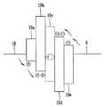
도 3은 일반적인 플렉서블 유기발광 디스플레이 장치의 구조를 예시적으로 보여주는 사시도로써, 연성 회로기판(Flexible Printed Circuit Board; FPCB)이 체결된 상태의 플렉서블 유기발광 디스플레이 장치를 예를 들어 나타내고 있다.FIG. 3 is a perspective view illustrating an example of a structure of a general flexible organic light emitting display device, and illustrates a flexible organic light emitting display device in a state where a flexible printed circuit board (FPCB) is fastened.
상기 도 3을 참조하면, 일반적으로 플렉서블 유기발광 디스플레이 장치는 크게 영상을 표시하는 패널 어셈블리와 상기 패널 어셈블리에 연결되는 연성 회로기판(30)을 포함한다.Referring to FIG. 3, a flexible organic light emitting display device generally includes a panel assembly displaying a large image and a
상기 패널 어셈블리는 TFT 기판(5)과 상기 TFT 기판(5) 위에 형성되는 보호 필름(barrier film)(4)을 포함한다.The panel assembly includes a
이때, 상기 TFT 기판(5)은 다수의 부화소(sub pixel)들이 배치되어 실제로 영상을 표시하는 표시부(AA) 및 상기 표시부(AA)의 외곽에 형성되어 외부로부터 인가되는 신호를 상기 표시부(AA) 내에 전달하는 외곽부로 구분할 수 있으며, 상기 보호 필름(4)은 상기 표시부(AA)와 외곽부 일부를 덮으면서 상기 TFT 기판(5) 위에 형성되게 된다.In this case, the
이때, 상기 보호 필름(4)에 의해 덮이지 않고 노출되는 외곽부는 패드가 형성되는 패드부(PA)를 구성한다.At this time, the outer portion exposed without being covered by the
상기 TFT 기판(5)으로 폴리이미드 기판을 적용할 수 있으며, 그 배면에는 백 플레이트(back plate)(10)가 부착되어 있다.A polyimide substrate can be applied to the
그리고, 상기 보호 필름(4) 위에는 외부로부터 입사된 광의 반사를 막기 위한 편광판(미도시)이 부착되어 있다.A polarizing plate (not shown) is attached to the
이때, 자세히 도시하지 않았지만, 상기 TFT 기판(5)의 표시부(AA)에는 부화소들이 매트릭스 형태로 배치되며, 상기 표시부(AA)의 외측, 즉 상기 외곽부에는 상기 부화소들을 구동시키기 위한 스캔 드라이버와 데이터 드라이버 등의 구동소자, 패드전극들 및 기타 부품들이 위치한다.In this case, although not shown in detail, sub-pixels are arranged in a matrix form on the display portion AA of the
상기 보호 필름(4)은 TFT 기판(5)에 형성된 유기발광다이오드들과 구동회로들 위에 형성되어 유기발광다이오드들과 구동회로들을 외부로부터 밀봉하여 보호한다.The
이렇게 구성된 상기 패널 어셈블리의 패드부(PA)에는 칩 온 글라스(chip on glass) 방식으로 집적회로 칩(미도시)이 실장 된다.An integrated circuit chip (not shown) is mounted on the pad part PA of the panel assembly configured as described above in a chip on glass manner.
상기 연성 회로기판(30)에는 구동 신호를 처리하기 위한 전자 소자(미도시)들이 칩 온 필름(chip on film) 방식으로 실장되고, 외부 신호를 연성 회로기판(30)으로 전송하기 위한 커넥터(미도시)가 설치된다.Electronic devices (not shown) for processing driving signals are mounted on the flexible printed
이러한 연성 회로기판(30)은 패널 어셈블리의 뒤쪽으로 접혀 연성 회로기판(30)이 패널 어셈블리의 배면과 마주하도록 한다. 즉, TFT 기판(5)에 보호 필름(4)이 합착되어 모듈 어셈블리를 구성하는 상태에서 벤딩부를 가진 연성 회로기판(30)이 접착층(미도시)을 통해 유기발광 디스플레이 장치의 배면에 부착되게 된다.The
이때, TFT 기판(5)의 단자부와 연성 회로기판(30)의 접속부가 서로 전기적으로 접속하도록 하기 위하여 이방성 도전필름(Anisotropic Conductive Film; ACF)(미도시)을 이용하게 된다.At this time, an anisotropic conductive film (ACF) (not shown) is used to electrically connect the terminal portion of the
이와 같이 구성되는 플렉서블 유기발광 디스플레이 장치는 상기 TFT 기판(5)과 보호 필름(4)을 글라스가 아닌 필름형태의 재료를 사용하여 구현한다.The flexible organic light emitting display device configured as described above implements the
이때, 상기 필름형태의 TFT 기판(5)과 보호 필름(4) 사이에는 점착층이 존재하여 플렉서블 디스플레이를 구현하기 위한 봉지 기술을 구현하며, 상기 필름형태의 TFT 기판(5) 하부에는 전술한 바와 같이 백 플레이트(10)를 점착제를 이용하여 접착시킴으로써 평평함을 유지할 수 있는 플렉서블 디스플레이를 구현하게 된다.In this case, an adhesive layer is present between the film-
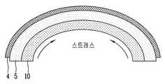
한편, 도 4는 플렉서블 유기발광 디스플레이 장치의 벤딩(bending) 시 스트레스에 의해 크랙이 발생하는 현상을 예시적으로 보여주는 도면이다.Meanwhile, FIG. 4 is a diagram exemplarily illustrating a phenomenon in which cracks occur due to stress during bending of the flexible organic light emitting display device.
상기 도 4를 참조하면, 이러한 플렉서블 유기발광 디스플레이 장치는 필름형태의 TFT 기판(5)과 보호 필름(4)의 평평함을 유지하기 위해 하부에 부착한 백 플레이트(10)와 봉지수단으로 상부에 부착한 상기 보호 필름(4), 그리고 최상부의 편광판이 가진 열 팽창력의 차이로 인하여 벤딩 시 패널 어셈블리에 스트레스가 가해지고, 이러한 스트레스는 패널 어셈블리의 가장 취약한 부분인 외곽부에 몰리게 되어 패널 어셈블리에 크랙(crack)이 발생하게 된다.Referring to FIG. 4, the flexible organic light emitting display device is attached to the upper portion with a
이러한 크랙은 상기 외곽부에서 가장 약한 부분인 보호층에서 발생하여 안으로 전파되기 때문에 벤딩 후 패널 어셈블리의 구동불량을 야기하는 문제점이 있다.This crack occurs in the protective layer, which is the weakest part of the outer part, and propagates therein, which causes a problem in driving the panel assembly after bending.
본 발명은 상기한 문제를 해결하기 위한 것으로, 벤딩 시 발생할 수 있는 크랙을 방지하는 동시에 수분 침투를 방지하도록 한 플렉서블 유기발광 디스플레이 장치를 제공하는데 목적이 있다.An object of the present invention is to provide a flexible organic light emitting display device which prevents water infiltration while preventing cracks that may occur when bending.
기타, 본 발명의 다른 목적 및 특징들은 후술되는 발명의 구성 및 특허청구범위에서 설명될 것이다.Other objects and features of the present invention will be described in the configuration and claims of the invention which will be described later.
상기한 목적을 달성하기 위하여, 본 발명의 플렉서블 유기발광 디스플레이 장치는 표시부와 외곽부로 구분되는 TFT 기판; 상기 표시부의 TFT 기판 위에 형성된 유기발광다이오드와 구동회로부; 상기 표시부의 TFT 기판과 최외곽 영역 이외의 상기 외곽부의 TFT 기판 위에 형성된 다수의 절연층; 상기 다수의 절연층이 형성된 TFT 기판 위에 상기 절연층을 덮으며, 일부가 더 연장되어 상기 TFT 기판 위에 직접 형성되는 1차 보호층; 상기 1차 보호층 위에 형성된 캡핑층(capping layer); 및 상기 표시부와 외곽부 일부를 덮으면서 상기 캡핑층이 형성된 TFT 기판 위에 부착되는 보호 필름(barrier film)을 포함하며, 상기 캡핑층은 그 상부의 상기 보호 필름의 외부까지 연장되어 벤딩(bending) 시 상기 1차 보호층이 받는 스트레스를 완화시키는 것을 특징으로 한다.In order to achieve the above object, the flexible organic light emitting display device of the present invention is a TFT substrate divided into a display portion and the outer portion; An organic light emitting diode and a driving circuit unit formed on the TFT substrate of the display unit; A plurality of insulating layers formed on the TFT substrate of the display unit and the TFT substrate of the outer portion other than the outermost region; A first protective layer covering the insulating layer on the TFT substrate on which the plurality of insulating layers are formed, a part of which is further extended to be formed directly on the TFT substrate; A capping layer formed on the primary protective layer; And a barrier film attached to the TFT substrate on which the capping layer is formed while covering a portion of the display portion and the outer portion, wherein the capping layer extends to the outside of the protective film on the upper side of the capping layer. It is characterized in that to reduce the stress received by the primary protective layer.
이때, 상기 TFT 기판은 폴리이미드(polyimide; PI) 기판으로 이루어진 것을 특징으로 한다.At this time, the TFT substrate is characterized in that made of a polyimide (PI) substrate.
상기 캡핑층 위에 형성되는 2차 보호층을 추가로 포함하는 것을 특징으로 한다.It characterized in that it further comprises a secondary protective layer formed on the capping layer.
이때, 상기 2차 보호층은 상기 캡핑층을 덮도록 상기 1차 보호층의 단부까지 연장, 형성되는 것을 특징으로 한다.In this case, the secondary protective layer is characterized in that extending to the end of the primary protective layer to cover the capping layer.
이때, 상기 2차 보호층은 수분이 상기 캡핑층을 타고 내부로 침투하는 것을 방지하는 것을 특징으로 한다.In this case, the secondary protective layer is characterized in that the moisture is prevented from penetrating inside the capping layer.
상기 보호 필름은 상기 2차 보호층 위에 점착층을 통해 부착되는 것을 특징으로 한다.The protective film is characterized in that the adhesive layer is attached on the secondary protective layer.
상기 보호 필름 위에 점착제를 통해 부착된 편광판을 추가로 포함하는 것을 특징으로 한다.It characterized in that it further comprises a polarizing plate attached on the protective film via an adhesive.
상기 캡핑층은 폴리머 등의 유기물질로 이루어진 것을 특징으로 한다.The capping layer is made of an organic material such as a polymer.
상기 표시부 및 외곽부에 형성되는 격벽을 추가로 포함하며, 상기 표시부 내의 격벽은 각 화소영역을 구획하는 것을 특징으로 한다.And a partition wall formed in the display unit and the outer portion, wherein the partition wall in the display unit partitions each pixel area.
이때, 상기 1차 보호층은 상기 격벽이 형성된 TFT 기판 위에 형성되는 한편, 상기 캡핑층은 상기 외곽부의 일정 영역까지 연장되어 상기 격벽을 완전히 덮는 것을 특징으로 한다.In this case, the primary protective layer is formed on the TFT substrate on which the partition wall is formed, while the capping layer extends to a predetermined region of the outer portion to completely cover the partition wall.
상술한 바와 같이, 본 발명에 따른 플렉서블 유기발광 디스플레이 장치는 캡핑층(capping layer)을 상부 점착층 외부까지 연장함으로써 1차 보호층이 받는 스트레스를 완화시켜 벤딩 시 발생할 수 있는 크랙을 방지하는 동시에 상기 캡핑층 위에 2차 보호층을 증착함으로써 수분 침투를 방지할 수 있게 된다. 이에 따라 수율이 향상되는 한편, 향후 제품 개발 시 벤딩에 대한 제한을 완화시킬 수 있는 효과를 제공한다.As described above, the flexible organic light emitting display device according to the present invention extends the capping layer to the outside of the upper adhesive layer to relieve stress of the primary protective layer to prevent cracks that may occur when bending. By depositing a second protective layer on the capping layer it is possible to prevent the penetration of moisture. As a result, the yield is improved, while also providing the effect of easing the restriction on bending in future product development.
도 1은 일반적인 유기발광 디스플레이 장치의 발광원리를 설명하는 다이어그램.
도 2는 일반적인 유기발광 디스플레이 장치에 있어, 하나의 화소에 대한 등가 회로도.
도 3은 일반적인 플렉서블 유기발광 디스플레이 장치의 구조를 예시적으로 보여주는 사시도.
도 4는 플렉서블 유기발광 디스플레이 장치의 벤딩 시 스트레스에 의해 크랙이 발생하는 현상을 예시적으로 보여주는 도면.
도 5는 본 발명의 제 1 실시예에 따른 플렉서블 유기발광 디스플레이 장치의 구조를 예시적으로 보여주는 사시도.
도 6은 상기 도 5에 도시된 본 발명의 제 1 실시예에 따른 플렉서블 유기발광 디스플레이 장치의 A-A'선에 따른 단면을 개략적으로 나타내는 도면.
도 7은 본 발명의 제 2 실시예에 따른 플렉서블 유기발광 디스플레이 장치의 단면을 개략적으로 나타내는 도면.
도 8a 및 도 8m은 상기 도 7에 도시된 본 발명의 제 2 실시예에 따른 플렉서블 유기발광 디스플레이 장치의 제조방법을 순차적으로 나타내는 단면도.1 is a diagram illustrating a light emission principle of a general organic light emitting display device.
2 is an equivalent circuit diagram of one pixel in a conventional organic light emitting display device.
3 is a perspective view illustrating an exemplary structure of a general flexible organic light emitting display device.
4 is a diagram illustrating a phenomenon in which cracks are generated by stress when bending the flexible organic light emitting display device.
5 is a perspective view illustrating a structure of a flexible organic light emitting display device according to a first embodiment of the present invention.
FIG. 6 is a schematic cross-sectional view taken along line AA ′ of the flexible organic light emitting display device according to the first embodiment of the present invention illustrated in FIG. 5.
FIG. 7 is a schematic cross-sectional view of a flexible organic light emitting display device according to a second embodiment of the present invention; FIG.
8A and 8M are cross-sectional views sequentially illustrating a method of manufacturing a flexible organic light emitting display device according to a second embodiment of the present invention shown in FIG. 7.
이하, 첨부한 도면을 참조하여 본 발명에 따른 플렉서블 유기발광 디스플레이 장치의 바람직한 실시예를 본 발명이 속하는 기술분야에서 통상의 지식을 가진 자가 용이하게 실시할 수 있도록 상세히 설명한다.Hereinafter, exemplary embodiments of the flexible organic light emitting display device according to the present invention will be described in detail with reference to the accompanying drawings so that those skilled in the art may easily implement the present invention.
본 발명의 이점 및 특징, 그리고 그것들을 달성하는 방법은 첨부되는 도면과 함께 상세하게 후술되어 있는 실시예들을 참조하면 명확해질 것이다. 그러나, 본 발명은 이하에서 개시되는 실시예들에 한정되는 것이 아니라 서로 다른 다양한 형태로 구현될 것이며, 단지 본 실시예들은 본 발명의 개시가 완전하도록 하며, 본 발명이 속하는 기술분야에서 통상의 지식을 가진 자에게 발명의 범주를 완전하게 알려주기 위해 제공되는 것이며, 본 발명은 청구항의 범주에 의해 정의될 뿐이다. 명세서 전체에 걸쳐 동일 참조 부호는 동일 구성요소를 지칭한다.Advantages and features of the present invention and methods for achieving them will be apparent with reference to the embodiments described below in detail with the accompanying drawings. However, the present invention is not limited to the embodiments disclosed below, but may be implemented in various different forms, only the present embodiments to make the disclosure of the present invention complete, and common knowledge in the art to which the present invention pertains. It is provided to fully inform the person having the scope of the invention, which is defined only by the scope of the claims. Like reference numerals refer to like elements throughout.
도 5는 본 발명의 제 1 실시예에 따른 플렉서블 유기발광 디스플레이 장치의 구조를 예시적으로 보여주는 사시도로써, 연성 회로기판이 체결된 상태의 플렉서블 유기발광 디스플레이 장치를 예를 들어 나타내고 있다.FIG. 5 is a perspective view illustrating a structure of a flexible organic light emitting display device according to a first exemplary embodiment of the present invention, and illustrates a flexible organic light emitting display device in a state where a flexible circuit board is fastened.
도 6은 상기 도 5에 도시된 본 발명의 제 1 실시예에 따른 플렉서블 유기발광 디스플레이 장치의 A-A'선에 따른 단면을 개략적으로 나타내는 도면이다.FIG. 6 is a schematic cross-sectional view taken along line AA ′ of the flexible organic light emitting display device according to the first embodiment of the present invention illustrated in FIG. 5.
상기 도면들을 참조하면, 본 발명의 제 1 실시예에 따른 플렉서블 유기발광 디스플레이 장치는 크게 영상을 표시하는 패널 어셈블리(100)와 상기 패널 어셈블리(100)에 연결되는 연성 회로기판(130)을 포함한다.Referring to the drawings, the flexible organic light emitting display device according to the first embodiment of the present invention includes a
상기 패널 어셈블리(100)는 TFT 기판(105)과 상기 TFT 기판(105) 위에 형성되는 보호 필름(104)을 포함한다.The
이때, 상기 보호 필름(104)은 폴리카보네이트(Polycarbonate; PC)나 사이클로올레핀폴리머(cycloolefin polymer; COP) 재질의 투명 필름 하부에 SiO, SiN, Al2O2 등의 무기 배리어 층이 증착된 필름을 의미한다.In this case, the
이때, 상기 TFT 기판(105)은 다수의 부화소들이 배치되어 실제로 영상을 표시하는 표시부(AA) 및 상기 표시부(AA)의 외곽에 형성되어 외부로부터 인가되는 신호를 상기 표시부(AA) 내에 전달하는 외곽부로 구분할 수 있으며, 상기 보호 필름(104)은 상기 표시부(AA)와 외곽부 일부를 덮으면서 상기 TFT 기판(105) 위에 형성되게 된다.In this case, the
이때, 상기 외곽부 중에 상기 보호 필름(104)에 의해 덮이지 않고 노출되는 부분은 패드가 형성되는 패드부(PA)를 구성하게 된다.In this case, a portion of the outer portion exposed without being covered by the
상기 부화소는 유기발광다이오드와 구동회로부로 이루어진다.The subpixel includes an organic light emitting diode and a driving circuit unit.
상기 유기발광다이오드는 제 1 전극(118)과 유기 화합물층(119) 및 제 2 전극(108)을 포함한다.The organic light emitting diode includes a
이때, 자세히 도시하지 않았지만, 상기 유기 화합물층(119)은 실제 발광이 이루어지는 발광층 이외에 정공 또는 전자의 캐리어를 발광층까지 효율적으로 전달하기 위한 다양한 유기 층들을 더 포함할 수 있다.In this case, although not shown in detail, the
상기 유기 층들은 상기 제 1 전극(118)과 발광층 사이에 위치하는 정공주입층 및 정공수송층, 상기 제 2 전극(108)과 발광층 사이에 위치하는 전자주입층 및 전자수송층을 포함할 수 있다.The organic layers may include a hole injection layer and a hole transport layer between the
이와 같이 플라스틱이나 스테인레스 스틸로 이루어진 TFT 기판(105) 상에 투명 산화물로 이루어진 제 1 전극(118)이 형성되며, 상기 제 1 전극(118) 위에는 순차적으로 유기 화합물층(119) 및 제 2 전극(108)이 적층되어 있다.As such, the
이때, 상기 TFT 기판(105)으로 글라스 이외의 폴리이미드(polyimide) 재질을 사용할 수 있으며, 이 경우 상기 TFT 기판(105) 배면에는 폴리에틸렌 테레프탈레이트(Polyethylene Terephthalate; PET)의 플라스틱으로 이루어진 백 플레이트(110)가 점착제(113)를 통해 부착될 수 있다.In this case, a polyimide material other than glass may be used as the
상기 구조를 기반으로 유기발광다이오드는 제 1 전극(118)에서 주입되는 정공과 제 2 전극(108)에서 주입되는 전자가 각각의 수송을 위한 수송층을 경유하여 발광층에서 결합한 후 낮은 에너지 준위로 이동하면서 상기 발광층에서의 에너지 차에 해당하는 파장의 빛을 생성하게 된다.Based on the structure, the organic light emitting diode moves to a low energy level after the holes injected from the
이때, 백색광의 발광을 위하여 상기 발광층은 더욱 구체적으로 적색발광층, 녹색발광층 및 청색발광층으로 이루어질 수 있다.In this case, in order to emit white light, the light emitting layer may be more specifically formed of a red light emitting layer, a green light emitting layer, and a blue light emitting layer.
그리고, 상기 구동회로부는 적어도 2개의 박막 트랜지스터와 적어도 하나의 스토리지 커패시터를 포함한다. 상기 박막 트랜지스터는 기본적으로 스위칭 트랜지스터와 구동 트랜지스터를 포함한다.The driving circuit unit includes at least two thin film transistors and at least one storage capacitor. The thin film transistor basically includes a switching transistor and a driving transistor.
도시하지 않았지만, 스위칭 트랜지스터는 스캔라인과 데이터라인에 연결되고, 스캔라인에 입력되는 스위칭 전압에 따라 데이터라인에 입력되는 데이터 전압을 구동 트랜지스터로 전송한다. 스토리지 커패시터는 스위칭 트랜지스터와 전원 라인에 연결되며, 스위칭 트랜지스터로부터 전송 받은 전압과 전원라인에 공급되는 전압의 차이에 해당하는 전압을 저장한다.Although not shown, the switching transistor is connected to the scan line and the data line, and transmits the data voltage input to the data line to the driving transistor according to the switching voltage input to the scan line. The storage capacitor is connected to the switching transistor and the power line, and stores a voltage corresponding to the difference between the voltage received from the switching transistor and the voltage supplied to the power line.
구동 트랜지스터는 전원 라인과 스토리지 커패시터에 연결되어 스토리지 커패시터에 저장된 전압과 문턱 전압의 차이의 제곱에 비례하는 출력 전류를 유기발광다이오드로 공급하고, 유기발광다이오드는 출력 전류에 의해 발광한다.The driving transistor is connected to the power line and the storage capacitor to supply an output current to the organic light emitting diode, which is proportional to the square of the difference between the voltage stored in the storage capacitor and the threshold voltage, and the organic light emitting diode emits light by the output current.
상기 구동 트랜지스터는 반도체층(124)과 게이트전극(121) 및 소오스/드레인전극(122, 123)을 포함하며, 유기발광다이오드의 제 1 전극(118)이 구동 트랜지스터의 드레인전극(123)에 연결될 수 있다. 즉, 상기 구동 트랜지스터는 상기 TFT 기판(105) 위에 형성된 버퍼층(115a), 상기 버퍼층(115a) 위에 형성된 반도체층(124), 상기 반도체층(124)이 형성된 TFT 기판(105) 위에 형성된 제 1 절연층(115b), 상기 제 1 절연층(115b) 위에 형성된 게이트전극(121), 상기 게이트전극(121)이 형성된 TFT 기판(105) 위에 형성된 제 2 절연층(115c) 및 상기 제 2 절연층(115c) 위에 형성되어 제 1 콘택홀을 통해 상기 반도체층(124)의 소오스/드레인영역과 전기적으로 접속하는 소오스/드레인전극(122, 123)으로 구성된다.The driving transistor includes a
이때, 상기 버퍼층(115a)은 단일 층 또는 복수의 층으로 이루어질 수 있으며, 상기 반도체층(124)은 수소화된 비정질 규소, 다결정 규소, 또는 IGZO(Indium Gallium Zinc Oxide)와 같은 산화물 반도체로 형성할 수 있다.In this case, the
상기 게이트전극(121)은 알루미늄(Al)이나 알루미늄 합금(Al alloy) 등 알루미늄 계열 금속, 은(Ag)이나 은 합금 등 은 계열 금속, 구리(Cu)나 구리 합금 등 구리 계열 금속, 몰리브덴(Mo)이나 몰리브덴 합금 등 몰리브덴 계열 금속, 크롬(Cr), 탄탈륨(Ta), 티타늄(Ti)과 같은 저저항 불투명 도전물질을 사용할 수 있다. 그러나, 이들은 물리적 성질이 다른 2개의 도전막을 포함하는 다층막 구조를 가질 수 있다.The
상기 제 1 절연층(115b)과 제 2 절연층(115c)은 질화규소(SiNx)나 이산화규소(SiO2)와 같은 무기절연물질로 이루어진 단일 층, 또는 상기 질화규소와 이산화규소로 이루어진 이중의 층으로 이루어질 수 있다.The first insulating
상기 소오스전극(122)과 드레인전극(123)은 알루미늄이나 알루미늄 합금 등 알루미늄 계열 금속, 은이나 은 합금 등 은 계열 금속, 구리나 구리 합금 등 구리 계열 금속, 몰리브덴이나 몰리브덴 합금 등 몰리브덴 계열 금속, 크롬, 탄탈륨, 티타늄과 같은 저저항 불투명 도전물질을 사용할 수 있다. 그러나, 이들은 물리적 성질이 다른 2개의 도전막을 포함하는 다층막 구조를 가질 수 있다.The
다만, 이러한 부화소의 구성은 전술한 예에 한정되지 않으며 다양하게 변형 가능하다.However, the configuration of such a subpixel is not limited to the above-described example and may be variously modified.
이렇게 구성된 상기 구동 트랜지스터가 형성된 TFT 기판(105) 위에는 제 3 절연층(115d)이 형성되며, 상기 제 3 절연층(115d)은 질화규소나 이산화규소와 같은 무기절연물질로 형성될 수 있다.A third insulating
한편, 외곽부의 TFT 기판(105)의 제 2 절연층(115c) 위에는 공통패드(131)가 형성된다. 상기 공통패드(131)는 외부의 신호를 표시부(AA) 내의 제 2 전극(108)에 인가하기 위한 것으로, 구동 트랜지스터의 소오스전극(122) 및 드레인전극(123)과 동일한 공정에 의해 형성될 수 있다.On the other hand, a
도시하지 않았지만, 상기 외곽부에는 구동 트랜지스터의 게이트전극(121)에 주사신호를 인가하는 게이트패드와 제 1 전극(118)에 신호를 인가하는 데이터패드가 형성된다.Although not shown, a gate pad for applying a scan signal to the
이때, 상기 구동 트랜지스터의 드레인전극(123)은 상기 제 3 절연층(115d)에 형성된 제 2 컨택홀을 통해 상기 제 1 전극(118)과 전기적으로 접속되며, 상기 외곽부의 공통패드(131)는 상기 제 3 절연층(115d)에 형성된 제 3 컨택홀을 통해 그 상부의 공통패드 전극(138)과 전기적으로 접속된다.In this case, the
상기 제 1 전극(118)과 공통패드 전극(138)은 인듐-틴-옥사이드(Indium Tin Oxide; ITO) 또는 인듐-징크-옥사이드(Indium Zinc Oxide; IZO) 등의 투명한 도전물질이나 알루미늄, 은 또는 그 합금 등의 반사성 도전물질로 이루어질 수 있다. 상기 제 1 전극(118)과 공통패드 전극(138)은 동일한 도전물질로 동일한 공정에 의해 형성될 수도 있지만, 다른 공정에 의해 서로 다른 종류의 도전물질로 형성될 수도 있다.The
그리고, 상기 표시부(AA) 내의 제 3 절연층(115d) 상부의 각 화소영역의 경계에는 격벽(115e)이 형성된다. 상기 격벽(115e)은 각 화소영역을 구획하여 인접하는 화소영역에서 출력되는 특정 컬러의 광이 혼합되어 출력되는 것을 방지하기 위한 것이다.A
이러한 격벽(115e)은 상기 외곽부의 공통패드 전극(138)을 외부로 노출시키는 상태로 상기 외곽부로 연장된다.The
전술한 유기발광다이오드는 유기 화합물층(119)은 상기 격벽(115e) 사이의 제 1 전극(118) 위에 형성된다.The organic light emitting diode described above is formed on the
상기 표시부(AA)의 유기 화합물층(119) 위에는 상기 제 2 전극(108)이 형성된다. 상기 제 2 전극(108)은 공통 전압을 인가 받으며, 칼슘(Ca), 바륨(Ba), 마그네슘(Mg), 알루미늄, 은 등을 포함하는 반사성 도전물질 또는 ITO, IZO 등의 투명한 도전물질로 이루어질 수 있다.The
이때, 외곽부에도 제 2 전극(108)이 형성된다. 외곽부의 제 2 전극(108)은 상기 공통패드 전극(138)을 통해 공통패드(131)와 접속되고, 표시부(AA)의 제 2 전극(108)과 연결되어 외부의 신호가 상기 공통패드(131)를 통해 제 2 전극(108)으로 인가된다.At this time, the
외곽부와 표시부(AA)의 제 2 전극(108) 및 격벽(115e) 상부에는 상기 TFT 기판(105) 전체에 걸쳐서 1차 보호층(passivation layer)(115f)이 형성된다. 상기 1차 보호층(115f)은 질화규소나 이산화규소와 같은 무기절연물질로 형성될 수 있다.A
또한, 상기 1차 보호층(115f) 위에는 폴리머 등의 유기물질로 이루어진 캡핑층(115g)이 형성된다.In addition, a
상기 캡핑층(115g) 위에는 점착층(103)이 형성되며, 그 위에 보호 필름(104)이 배치되어, 상기 점착층(103)에 의해 보호 필름(104)이 부착된다.An
이때, 상기 본 발명의 제 1 실시예에 따른 캡핑층(115g)은 플렉서블 유기발광 디스플레이 장치를 벤딩 시 발생할 수 있는 응력을 완화하고자 그 상부의 점착층(103) 외부까지 연장, 형성하는 것을 특징으로 한다. 즉, 기존에는 벤딩 시 발생하는 스트레스를 1차 보호층(115f)이 모두 받게 되어 손상 및 크랙이 발생하게 되나, 본 발명의 제 1 실시예와 같이 상기 캡핑층(115g)의 증착 영역을 상부의 점착층(103) 외부까지 연장함으로써 상기 1차 보호층(115f)이 받는 스트레스를 완화시켜 크랙을 미연에 방지할 수 있게 된다.In this case, the
상기 보호 필름(104)의 상부에는 외부로부터 입사된 광의 반사를 막기 위한 편광판(101)이 점착제(미도시)를 통해 부착될 수 있다.The
이렇게 구성된 상기 패널 어셈블리(100)의 패드부(PA)에는 칩 온 글라스 방식으로 집적회로 칩(미도시)이 실장될 수 있다.An integrated circuit chip (not shown) may be mounted on the pad part PA of the
상기 연성 회로기판(130)에는 구동 신호를 처리하기 위한 전자 소자(미도시)들이 칩 온 필름 방식으로 실장되고, 외부 신호를 연성 회로기판(130)으로 전송하기 위한 커넥터(미도시)가 설치될 수 있다.Electronic devices (not shown) for processing driving signals may be mounted on the
이러한 연성 회로기판(130)은 패널 어셈블리(100)의 뒤쪽으로 접혀 연성 회로기판(130)이 패널 어셈블리(100)의 배면과 마주하도록 한다. 즉, TFT 기판(105)에 보호 필름(104)이 합착되어 모듈 어셈블리를 구성하는 상태에서 벤딩부를 가진 연성 회로기판(130)이 접착층(미도시)을 통해 유기발광 디스플레이 장치의 배면에 부착되게 된다.The
이때, TFT 기판(105)의 단자부와 연성 회로기판(130)의 접속부가 서로 전기적으로 접속하도록 하기 위하여 이방성 도전필름(미도시)을 이용할 수 있다.In this case, an anisotropic conductive film (not shown) may be used to electrically connect the terminal portion of the
이와 같이 본 발명의 제 1 실시예에서는 캡핑층을 점착층 외부까지 연장, 증착 시킴으로써 벤딩 시 1차 보호층에 가해지는 스트레스를 완화시키는 것을 특징으로 한다. 다만, 이 경우에는 캡핑층이 외부에 노출되게 됨에 따라 수분이 상기 캡핑층을 타고 내부로 침투할 가능성이 있으며, 이에 본 발명의 제 2 실시예에서는 상기 캡핑층 위에 2차 보호층을 증착 시키게 되며, 이를 다음의 도면을 통해 상세히 설명한다.As described above, in the first embodiment of the present invention, the capping layer is extended and deposited to the outside of the adhesive layer to relieve stress applied to the primary protective layer during bending. However, in this case, as the capping layer is exposed to the outside, moisture may penetrate inside the capping layer, and accordingly, in the second embodiment of the present invention, a secondary protective layer is deposited on the capping layer. This will be described in detail with reference to the following drawings.
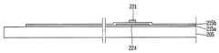
도 7은 본 발명의 제 2 실시예에 따른 플렉서블 유기발광 디스플레이 장치의 단면을 개략적으로 나타내는 도면으로써, 외곽부와 외곽부에 인접한 표시부의 일부 구성을 예를 들어 나타내고 있다.FIG. 7 is a schematic cross-sectional view of a flexible organic light emitting display device according to a second exemplary embodiment of the present invention. FIG. 7 illustrates an example of an outer portion and a part of a display unit adjacent to the outer portion.
이때, 상기 도 7에 도시된 본 발명의 제 2 실시예에 따른 플렉서블 유기발광 디스플레이 장치는 캡핑층 위에 상기 캡핑층을 덮도록 2차 보호층을 증착하는 것을 제외하고는 실질적으로 전술한 본 발명의 제 1 실시예와 동일한 구성으로 이루어져 있다.In this case, the flexible organic light emitting display device according to the second embodiment of the present invention illustrated in FIG. 7 is substantially the same as that of the present invention except for depositing a secondary protective layer on the capping layer to cover the capping layer. It consists of the same structure as 1st Embodiment.
상기 도 7을 참조하면, 본 발명의 제 2 실시예에 따른 플렉서블 유기발광 디스플레이 장치는 크게 영상을 표시하는 패널 어셈블리(200)와 상기 패널 어셈블리(200)에 연결되는 연성 회로기판(미도시)을 포함한다.Referring to FIG. 7, the flexible organic light emitting display device according to the second embodiment of the present invention includes a
상기 패널 어셈블리(200)는 TFT 기판(205)과 상기 TFT 기판(205) 위에 형성되는 보호 필름(204)을 포함한다.The
이때, 상기 보호 필름(204)은 폴리카보네이트나 사이클로올레핀폴리머 재질의 투명 필름 하부에 SiO, SiN, Al2O2 등의 무기 배리어 층이 증착된 필름을 의미한다.At this time, the
이때, 상기 TFT 기판(205)은 다수의 부화소들이 배치되어 실제로 영상을 표시하는 표시부 및 상기 표시부의 외곽에 형성되어 외부로부터 인가되는 신호를 상기 표시부 내에 전달하는 외곽부로 구분할 수 있으며, 상기 보호 필름(204)은 상기 표시부와 외곽부 일부를 덮으면서 상기 TFT 기판(205) 위에 형성되게 된다.In this case, the
이때, 상기 외곽부 중에 상기 보호 필름(204)에 의해 덮이지 않고 노출되는 부분은 패드가 형성되는 패드부(미도시)를 구성하게 된다.In this case, a portion of the outer portion exposed without being covered by the
전술한 바와 같이 상기 부화소는 유기발광다이오드와 구동회로부로 이루어진다.As described above, the subpixel includes an organic light emitting diode and a driving circuit unit.
상기 유기발광다이오드는 제 1 전극(218)과 유기 화합물층(219) 및 제 2 전극(208)을 포함한다.The organic light emitting diode includes a
이때, 자세히 도시하지 않았지만, 상기 유기 화합물층(219)은 실제 발광이 이루어지는 발광층 이외에 정공 또는 전자의 캐리어를 발광층까지 효율적으로 전달하기 위한 다양한 유기 층들을 더 포함할 수 있다.In this case, although not shown in detail, the
상기 유기 층들은 상기 제 1 전극(218)과 발광층 사이에 위치하는 정공주입층 및 정공수송층, 상기 제 2 전극(208)과 발광층 사이에 위치하는 전자주입층 및 전자수송층을 포함할 수 있다.The organic layers may include a hole injection layer and a hole transport layer between the
이와 같이 플라스틱이나 스테인레스 스틸로 이루어진 TFT 기판(205) 상에 투명 산화물로 이루어진 제 1 전극(218)이 형성되며, 상기 제 1 전극(218) 위에는 순차적으로 유기 화합물층(219) 및 제 2 전극(208)이 적층되어 있다.As such, a
이때, 상기 TFT 기판(205)으로 글라스 이외의 폴리이미드 재질을 사용할 수 있으며, 이 경우 상기 TFT 기판(205) 배면에는 폴리에틸렌 테레프탈레이트의 플라스틱으로 이루어진 백 플레이트(205)가 점착제(213)를 통해 부착될 수 있다.In this case, a polyimide material other than glass may be used as the
상기 구조를 기반으로 유기발광다이오드는 제 1 전극(218)에서 주입되는 정공과 제 2 전극(208)에서 주입되는 전자가 각각의 수송을 위한 수송층을 경유하여 발광층에서 결합한 후 낮은 에너지 준위로 이동하면서 상기 발광층에서의 에너지 차에 해당하는 파장의 빛을 생성하게 된다.Based on the structure, the organic light emitting diode moves to a low energy level after the holes injected from the
이때, 백색광의 발광을 위하여 상기 발광층은 더욱 구체적으로 적색발광층, 녹색발광층 및 청색발광층으로 이루어질 수 있다.In this case, in order to emit white light, the light emitting layer may be more specifically formed of a red light emitting layer, a green light emitting layer, and a blue light emitting layer.
그리고, 상기 구동회로부는 적어도 2개의 박막 트랜지스터와 적어도 하나의 스토리지 커패시터를 포함한다. 상기 박막 트랜지스터는 기본적으로 스위칭 트랜지스터와 구동 트랜지스터를 포함한다.The driving circuit unit includes at least two thin film transistors and at least one storage capacitor. The thin film transistor basically includes a switching transistor and a driving transistor.
도시하지 않았지만, 스위칭 트랜지스터는 스캔라인과 데이터라인에 연결되고, 스캔라인에 입력되는 스위칭 전압에 따라 데이터라인에 입력되는 데이터 전압을 구동 트랜지스터로 전송한다. 스토리지 커패시터는 스위칭 트랜지스터와 전원 라인에 연결되며, 스위칭 트랜지스터로부터 전송 받은 전압과 전원라인에 공급되는 전압의 차이에 해당하는 전압을 저장한다.Although not shown, the switching transistor is connected to the scan line and the data line, and transmits the data voltage input to the data line to the driving transistor according to the switching voltage input to the scan line. The storage capacitor is connected to the switching transistor and the power line, and stores a voltage corresponding to the difference between the voltage received from the switching transistor and the voltage supplied to the power line.
구동 트랜지스터는 전원 라인과 스토리지 커패시터에 연결되어 스토리지 커패시터에 저장된 전압과 문턱 전압의 차이의 제곱에 비례하는 출력 전류를 유기발광다이오드로 공급하고, 유기발광다이오드는 출력 전류에 의해 발광한다.The driving transistor is connected to the power line and the storage capacitor to supply an output current to the organic light emitting diode, which is proportional to the square of the difference between the voltage stored in the storage capacitor and the threshold voltage, and the organic light emitting diode emits light by the output current.
상기 구동 트랜지스터는 반도체층(224)과 게이트전극(221) 및 소오스/드레인전극(222, 223)을 포함하며, 유기발광다이오드의 제 1 전극(218)이 구동 트랜지스터의 드레인전극(223)에 연결될 수 있다. 즉, 상기 구동 트랜지스터는 상기 TFT 기판(205) 위에 형성된 버퍼층(215a), 상기 버퍼층(215a) 위에 형성된 반도체층(224), 상기 반도체층(224)이 형성된 TFT 기판(205) 위에 형성된 제 1 절연층(215b), 상기 제 1 절연층(215b) 위에 형성된 게이트전극(221), 상기 게이트전극(221)이 형성된 TFT 기판(205) 위에 형성된 제 2 절연층(215c) 및 상기 제 2 절연층(215c) 위에 형성되어 제 1 콘택홀을 통해 상기 반도체층(224)의 소오스/드레인영역과 전기적으로 접속하는 소오스/드레인전극(222, 223)으로 구성된다.The driving transistor includes a
이때, 상기 버퍼층(215a)은 단일 층 또는 복수의 층으로 이루어질 수 있으며, 상기 반도체층(224)은 수소화된 비정질 규소, 다결정 규소, 또는 IGZO와 같은 산화물 반도체로 형성할 수 있다.In this case, the
상기 게이트전극(221)은 알루미늄이나 알루미늄 합금 등 알루미늄 계열 금속, 은이나 은 합금 등 은 계열 금속, 구리나 구리 합금 등 구리 계열 금속, 몰리브덴이나 몰리브덴 합금 등 몰리브덴 계열 금속, 크롬, 탄탈륨, 티타늄과 같은 저저항 불투명 도전물질을 사용할 수 있다. 그러나, 이들은 물리적 성질이 다른 2개의 도전막을 포함하는 다층막 구조를 가질 수 있다.The
상기 제 1 절연층(215b)과 제 2 절연층(215c)은 질화규소나 이산화규소와 같은 무기절연물질로 이루어진 단일 층, 또는 상기 질화규소와 이산화규소로 이루어진 이중의 층으로 이루어질 수 있다.The first insulating
상기 소오스전극(222)과 드레인전극(223)은 알루미늄이나 알루미늄 합금 등 알루미늄 계열 금속, 은이나 은 합금 등 은 계열 금속, 구리나 구리 합금 등 구리 계열 금속, 몰리브덴이나 몰리브덴 합금 등 몰리브덴 계열 금속, 크롬, 탄탈륨, 티타늄과 같은 저저항 불투명 도전물질을 사용할 수 있다. 그러나, 이들은 물리적 성질이 다른 2개의 도전막을 포함하는 다층막 구조를 가질 수 있다.The
다만, 전술한 바와 같이 이러한 부화소의 구성은 전술한 예에 한정되지 않으며 다양하게 변형 가능하다.However, as described above, the configuration of such a subpixel is not limited to the above-described example and may be variously modified.
이렇게 구성된 상기 구동 트랜지스터가 형성된 TFT 기판(205) 위에는 제 3 절연층(215d)이 형성되며, 상기 제 3 절연층(215d)은 질화규소나 이산화규소와 같은 무기절연물질로 형성될 수 있다.A third insulating
한편, 외곽부의 TFT 기판(205)의 제 2 절연층(215c) 위에는 공통패드(231)가 형성된다. 상기 공통패드(231)는 외부의 신호를 표시부 내의 제 2 전극(208)에 인가하기 위한 것으로, 구동 트랜지스터의 소오스전극(222) 및 드레인전극(223)과 동일한 공정에 의해 형성될 수 있다.On the other hand, a
도시하지 않았지만, 상기 외곽부에는 구동 트랜지스터의 게이트전극(221)에 주사신호를 인가하는 게이트패드와 제 1 전극(218)에 신호를 인가하는 데이터패드가 형성된다.Although not shown, a gate pad for applying a scan signal to the
이때, 상기 구동 트랜지스터의 드레인전극(223)은 상기 제 3 절연층(215d)에 형성된 제 2 컨택홀을 통해 상기 제 1 전극(218)과 전기적으로 접속되며, 상기 외곽부의 공통패드(231)는 상기 제 3 절연층(215d)에 형성된 제 3 컨택홀을 통해 그 상부의 공통패드 전극(238)과 전기적으로 접속된다.In this case, the
상기 제 1 전극(218)과 공통패드 전극(238)은 ITO 또는 IZO 등의 투명한 도전물질이나 알루미늄, 은 또는 그 합금 등의 반사성 도전물질로 이루어질 수 있다. 상기 제 1 전극(218)과 공통패드 전극(238)은 동일한 도전물질로 동일한 공정에 의해 형성될 수도 있지만, 다른 공정에 의해 서로 다른 종류의 도전물질로 형성될 수도 있다.The
그리고, 상기 표시부 내의 제 3 절연층(215d) 상부의 각 화소영역의 경계에는 격벽(215e)이 형성된다. 상기 격벽(215e)은 각 화소영역을 구획하여 인접하는 화소영역에서 출력되는 특정 컬러의 광이 혼합되어 출력되는 것을 방지하기 위한 것이다.A
이러한 격벽(215e)은 상기 외곽부의 공통패드 전극(238)을 외부로 노출시키는 상태로 상기 외곽부로 연장된다.The
전술한 유기발광다이오드는 유기 화합물층(219)은 상기 격벽(215e) 사이의 제 1 전극(218) 위에 형성된다.The organic light emitting diode described above is formed on the
상기 표시부의 유기 화합물층(219) 위에는 상기 제 2 전극(208)이 형성된다. 상기 제 2 전극(208)은 공통 전압을 인가 받으며, 칼슘, 바륨, 마그네슘, 알루미늄, 은 등을 포함하는 반사성 도전물질 또는 ITO, IZO 등의 투명한 도전물질로 이루어질 수 있다.The
이때, 외곽부에도 제 2 전극(208)이 형성된다. 외곽부의 제 2 전극(208)은 상기 공통패드 전극(238)을 통해 공통패드(231)와 접속되고, 표시부의 제 2 전극(208)과 연결되어 외부의 신호가 상기 공통패드(231)를 통해 제 2 전극(208)으로 인가된다.At this time, the
외곽부와 표시부의 제 2 전극(208) 및 격벽(215e) 상부에는 상기 TFT 기판(205) 전체에 걸쳐서 1차 보호층(215f)이 형성된다. 상기 1차 보호층(215f)은 질화규소나 이산화규소와 같은 무기절연물질로 형성될 수 있다.The primary
또한, 상기 1차 보호층(215f) 위에는 폴리머 등의 유기물질로 이루어진 캡핑층(215g)이 형성된다.In addition, a
상기 캡핑층(215g) 위에는 상기 캡핑층(215g)을 덮도록 2차 보호층(215h)이 형성된다. 그리고, 점착층(203)이 형성되며, 그 위에 상기 보호 필름(204)이 배치되어, 상기 점착층(203)에 의해 보호 필름(204)이 부착된다.The secondary
그리고, 상기 보호 필름(204) 위에는 외부로부터 입사된 광의 반사를 막기 위한 편광판(201)이 점착제(미도시)를 통해 부착될 수 있다.The
이때, 상기 본 발명의 제 2 실시예에 따른 캡핑층(215g)은 전술한 제 1 실시예와 동일하게 플렉서블 유기발광 디스플레이 장치를 벤딩 시 발생할 수 있는 응력을 완화하고자 그 상부의 점착층(203) 외부까지 연장, 형성하는 것을 특징으로 한다. 이와 같이 상기 캡핑층(215g)의 증착 영역을 상부의 점착층(203) 외부까지 연장함으로써 상기 1차 보호층(215f)이 받는 스트레스를 완화시켜 크랙을 미연에 방지할 수 있게 된다.At this time, the
특히, 상기 본 발명의 제 2 실시예는 상기 캡핑층(215g)의 상부에 상기 캡핑층(215g)을 덮도록 2차 보호층(215h)을 증착함으로써 수분이 상기 캡핑층(215g)을 타고 내부로 침투하는 것을 원천적으로 방지할 수 있게 된다.Particularly, in the second embodiment of the present invention, the second
이하, 상기와 같이 구성되는 본 발명의 제 2 실시예에 따른 플렉서블 유기발광 디스플레이 장치의 제조방법을 도면을 참조하여 상세히 설명한다.Hereinafter, a method of manufacturing the flexible organic light emitting display device according to the second embodiment of the present invention configured as described above will be described in detail with reference to the accompanying drawings.
도 8a 및 도 8m은 상기 도 7에 도시된 본 발명의 제 2 실시예에 따른 플렉서블 유기발광 디스플레이 장치의 제조방법을 순차적으로 나타내는 단면도이다.8A and 8M are cross-sectional views sequentially illustrating a method of manufacturing a flexible organic light emitting display device according to a second embodiment of the present invention shown in FIG. 7.
도 8a에 도시된 바와 같이, 투명한 유리 또는 플라스틱 등의 절연물질로 이루어진 TFT 기판(205) 위에 버퍼층(buffer layer)(215a)과 규소막을 형성한다.As shown in FIG. 8A, a
이때, 상기 버퍼층(215a)은 단일 층 또는 복수의 층으로 형성할 수 있으며, 상기 TFT 기판(205) 내에 존재하는 나트륨(natrium; Na) 등의 불순물이 공정 중에 상부 층으로 침투하는 것을 차단하는 역할을 한다.In this case, the
상기 규소막은 비정질 규소 또는 다결정 규소로 형성할 수 있으나, 상기 본 발명의 실시예에서는 다결정 규소를 이용하여 박막 트랜지스터를 구성한 경우를 예를 들어 나타내고 있다. 이때, 상기 다결정 규소는 TFT 기판(205) 위에 비정질 규소를 증착한 후 여러 가지 결정화 방식을 이용하여 형성할 수 있다.The silicon film may be formed of amorphous silicon or polycrystalline silicon, but in the embodiment of the present invention, a thin film transistor is formed using polycrystalline silicon, for example. In this case, the polycrystalline silicon may be formed using various crystallization methods after depositing amorphous silicon on the
이후, 포토리소그래피공정을 통해 상기 규소막을 선택적으로 제거함으로써 상기 표시부에 상기 다결정 규소로 이루어진 액티브층(224)을 형성한다.Thereafter, the silicon film is selectively removed through a photolithography process to form an
이때, 전술한 바와 같이 상기 본 발명의 제 2 실시예는 상기 액티브층(224)을 다결정 규소로 형성한 경우를 예를 들어 나타내고 있으나, 본 발명이 이에 한정되는 것은 아니며, 상기 액티브층(224)은 수소화된 비정질 규소 또는 산화물 반도체로 이루어질 수 있다.In this case, as described above, the second embodiment of the present invention illustrates a case in which the
한편, 상기 액티브층(224)으로 수소화된 비정질 규소를 이용하는 경우에는 상기 비정질 규소와 함께 n+ 비정질 규소를 증착하여 패터닝함으로써 저항성 접촉 부재를 형성하게 되며, 이 경우에는 코플라나(coplanar) 구조 대신에 탑 게이트(top gate) 구조로 박막 트랜지스터를 형성할 수 있다. 이와 같이 본 발명은 상기 액티브층(224)을 구성하는 물질 및 그에 따른 박막 트랜지스터의 구조에 관계없이 적용 가능하다.Meanwhile, in the case of using the hydrogenated amorphous silicon as the
다음으로, 도 8b에 도시된 바와 같이, 상기 액티브층(224)이 형성된 TFT 기판(205) 위에 질화규소 또는 이산화규소 등으로 이루어진 제 1 절연층(215b)을 형성하며, 그 위에 게이트전극(221)과 게이트라인(미도시) 및 유지전극(미도시)을 형성한다.Next, as shown in FIG. 8B, a first insulating
상기 게이트전극(221)과 게이트라인 및 유지전극은 제 1 도전막을 상기 TFT 기판(205) 전면에 증착한 후 포토리소그래피공정을 통해 선택적으로 패터닝하여 형성하게 된다.The
여기서, 상기 제 1 도전막으로 알루미늄(Al)이나 알루미늄 합금(Al alloy) 등 알루미늄 계열 금속, 은(Ag)이나 은 합금 등 은 계열 금속, 구리(Cu)나 구리 합금 등 구리 계열 금속, 몰리브덴(Mo)이나 몰리브덴 합금 등 몰리브덴 계열 금속, 크롬(Cr), 탄탈륨(Ta), 티타늄(Ti)과 같은 저저항 불투명 도전물질을 사용할 수 있다. 그러나, 이들은 물리적 성질이 다른 2개의 도전막을 포함하는 다층막 구조를 가질 수 있다. 이 중 한 도전막은 신호 지연이나 전압 강하를 줄일 수 있도록 낮은 비저항(resistivity)의 금속, 예를 들면 알루미늄 계열 금속, 은 계열 금속, 구리 계열 금속 등으로 만들어질 수 있다. 이와는 달리, 다른 도전막은 다른 물질, 특히 ITO 및 IZO와의 물리적, 화학적, 전기적 접촉 특성이 우수한 물질, 예를 들면 몰리브덴 계열 금속, 크롬, 티타늄, 탄탈륨 등으로 만들어질 수 있다.Here, the first conductive film may include aluminum-based metals such as aluminum (Al) and aluminum alloys, silver-based metals such as silver (Ag) and silver alloys, copper-based metals such as copper (Cu) and copper alloys, and molybdenum ( Molybdenum-based metals such as Mo) and molybdenum alloys, and low resistance opaque conductive materials such as chromium (Cr), tantalum (Ta) and titanium (Ti) can be used. However, they may have a multilayer film structure including two conductive films having different physical properties. One of the conductive layers may be made of a low resistivity metal such as an aluminum-based metal, a silver-based metal, or a copper-based metal so as to reduce signal delay or voltage drop. Alternatively, other conductive films may be made of other materials, particularly materials having excellent physical, chemical, and electrical contact properties with ITO and IZO, such as molybdenum-based metals, chromium, titanium, tantalum, and the like.
상기 게이트전극(221)과 게이트라인 및 유지전극의 측면은 TFT 기판(205) 면에 대하여 경사질 수 있으며, 그 경사각은 약 30° 내지 약 80°인 것이 바람직하다.Sidewalls of the
다음으로, 도 8c에 도시된 바와 같이, 상기 게이트전극(221)과 게이트라인 및 유지전극이 형성된 TFT 기판(205) 전면에 질화규소 또는 이산화규소 등으로 이루어진 제 2 절연층(215c)을 형성한 후, 포토리소그래피공정을 통해 상기 제 2 절연층(215c)과 제 1 절연층(215b)을 선택적으로 제거하여 상기 액티브층(224)의 소오스/드레인영역을 노출시키는 제 1 콘택홀(240a)을 형성한다.Next, as shown in FIG. 8C, after the second insulating
이때, 외곽부에도 상기 버퍼층(215a)과 제 1 절연층(215b) 및 제 2 절연층(215c)이 형성되지만, 외곽부의 최외곽 영역에는 상기 버퍼층(215a)과 제 1 절연층(215b) 및 제 2 절연층(215c)이 형성되지 않는다.In this case, the
그리고, 도 8d에 도시된 바와 같이, 상기 제 2 절연층(215c)이 형성된 TFT 기판(205) 전면에 제 2 도전막을 형성한 후, 포토리소그래피공정을 통해 상기 제 2 도전막을 선택적으로 제거함으로써 상기 제 2 도전막으로 이루어진 데이터라인(미도시)과 구동 전압라인(미도시) 및 소오스/드레인전극(222, 223)을 형성한다.As shown in FIG. 8D, after the second conductive film is formed over the
이때, 상기 외곽부에는 상기 데이터 배선용 금속으로 이루어진 공통패드(231)가 형성될 수 있다.In this case, a
상기 소오스전극(222)과 드레인전극(223)은 상기 게이트전극(221)을 중심으로 서로 마주보는 한편, 상기 소오스/드레인전극(222, 223)은 상기 제 1 콘택홀을 통해 상기 액티브층(224)의 소오스/드레인영역에 전기적으로 접속하게 된다.The
이때, 상기 제 2 도전막으로 알루미늄이나 알루미늄 합금 등 알루미늄 계열 금속, 은이나 은 합금 등 은 계열 금속, 구리나 구리 합금 등 구리 계열 금속, 몰리브덴이나 몰리브덴 합금 등 몰리브덴 계열 금속, 크롬, 탄탈륨, 티타늄과 같은 저저항 불투명 도전물질을 사용할 수 있다. 그러나, 이들은 물리적 성질이 다른 2개의 도전막을 포함하는 다층막 구조를 가질 수 있다. 이 중 한 도전막은 신호 지연이나 전압 강하를 줄일 수 있도록 낮은 비저항의 금속, 예를 들면 알루미늄 계열 금속, 은 계열 금속, 구리 계열 금속 등으로 만들어질 수 있다. 이와는 달리, 다른 도전막은 다른 물질, 특히 ITO 및 IZO와의 물리적, 화학적, 전기적 접촉 특성이 우수한 물질, 예를 들면 몰리브덴 계열 금속, 크롬, 티타늄, 탄탈륨 등으로 만들어질 수 있다.In this case, the second conductive film may include aluminum-based metals such as aluminum or aluminum alloys, silver-based metals such as silver or silver alloys, copper-based metals such as copper or copper alloys, molybdenum-based metals such as molybdenum and molybdenum alloys, chromium, tantalum, and titanium; The same low resistance opaque conductive material can be used. However, they may have a multilayer film structure including two conductive films having different physical properties. One of the conductive layers may be made of a low resistivity metal, such as aluminum-based metal, silver-based metal, or copper-based metal, so as to reduce signal delay or voltage drop. Alternatively, other conductive films may be made of other materials, particularly materials having excellent physical, chemical, and electrical contact properties with ITO and IZO, such as molybdenum-based metals, chromium, titanium, tantalum, and the like.
상기 데이터라인, 구동 전압라인, 소오스/드레인전극(222, 223) 및 공통패드(231) 또한 그 측면이 TFT 기판(205) 면에 대하여 약 30° 내지 80° 정도의 경사각으로 기울어진 것이 바람직하다.The data line, the driving voltage line, the source /
다음으로, 도 8e에 도시된 바와 같이, 상기 데이터라인, 구동 전압라인, 소오스/드레인전극(222, 223) 및 공통패드(231)가 형성된 TFT 기판(205) 전면에 질화규소 또는 이산화규소 등으로 이루어진 제 3 절연층(215d)을 형성한다.Next, as shown in FIG. 8E, silicon nitride or silicon dioxide is formed on the
이후, 포토리소그래피공정을 통해 상기 제 3 절연층(215d)을 선택적으로 제거하여 상기 드레인전극(223)을 노출시키는 제 2 콘택홀(240b)을 형성하는 한편, 상기 외곽부의 제 3 절연층(215d)을 선택적으로 제거하여 상기 공통패드(231)를 노출시키는 제 3 콘택홀(240c)을 형성한다.Thereafter, the third insulating
또한, 상기 제 3 절연층(215d)은 외곽부의 최외곽 영역에는 형성되지 않으며, 일 예로 상기 제 3 절연층(215d)은 그 하부의 제 2 절연층(215c)보다 더 안쪽으로 형성될 수 있다.In addition, the third insulating
그리고, 도 8f에 도시된 바와 같이, 상기 제 3 절연층(215d)이 형성된 TFT 기판(205) 전면에 제 3 도전막을 증착한 후, 포토리소그래피공정을 통해 상기 제 3 도전막을 선택적으로 제거하여 상기 제 3 도전막으로 이루어진 화소전극(218)과 연결전극(미도시)을 형성한다.8F, after depositing a third conductive film over the
이때, 상기 애노드용 금속을 이용하여 상기 공통패드(231) 위에 공통패드 전극(238)을 형성한다.In this case, the
상기 제 3 도전막은 ITO 또는 IZO 등의 투명한 도전물질로 이루어질 수 있다.The third conductive layer may be made of a transparent conductive material such as ITO or IZO.
애노드인 상기 화소전극(218)은 상기 제 2 콘택홀을 통해 상기 드레인전극(223)과 전기적으로 접속하는 한편, 상기 공통패드 전극(238)은 상기 제 3 콘택홀을 통해 상기 공통패드(231)와 전기적으로 접속하게 된다.An anode of the
다음으로, 도 8g에 도시된 바와 같이, 상기 표시부 및 외곽부에 격벽(215e)을 형성한다.Next, as shown in FIG. 8G, a
이때, 상기 표시부 내의 격벽(215e)은 각 화소영역을 구획하여 인접하는 화소영역에서 출력되는 특정 컬러의 광이 혼합되어 출력되는 것을 방지하며, 유기 절연물질 또는 무기 절연물질로 만들어진다. 상기 격벽(215e)은 또한 검정색 안료를 포함하는 감광제로 만들어질 수 있는데, 이 경우 격벽(215e)은 차광부재의 역할을 하게 된다.In this case, the
이러한 격벽(215e)은 상기 외곽부의 공통패드 전극(238)을 외부로 노출시키도록 상기 외곽부로 연장되어 있으나, 본 발명이 이에 한정되는 것은 아니다.The
그리고, 도 8h에 도시된 바와 같이, 상기 격벽(215e)이 형성된 표시부의 TFT 기판(205) 위에 소정의 유기발광층(219)을 형성한다.8H, a predetermined organic
전술한 바와 같이 상기 유기발광층(219)은 빛을 내는 발광층 외에 발광층의 발광 효율을 향상하기 위한 부대층을 포함하는 다층 구조를 가질 수 있다. 상기 부대층에는 전자와 정공의 균형을 맞추기 위한 전자수송층 및 정공수송층과 전자와 정공의 주입을 강화하기 위한 전자주입층 및 정공주입층 등이 있다.As described above, the organic
다음으로, 도 8i에 도시된 바와 같이, 상기 유기발광층(219)이 형성된 TFT 기판(205) 위에 캐소드인 공통전극(208)을 형성한다.Next, as shown in FIG. 8I, a
이때, 상기 공통전극(208)을 구성하는 캐소드용 금속은 노출된 상기 공통패드(231)와 전기적으로 접속하게 되며, 따라서 상기 공통전극(208)은 상기 공통패드(231)를 통해 공통 전압을 인가 받게 된다. 이러한 상기 공통전극(208)은 칼슘, 바륨, 마그네슘, 알루미늄, 은 등을 포함하는 반사성 도전물질 또는 ITO, IZO 등의 투명한 도전물질로 이루어질 수 있다.In this case, the cathode metal constituting the
이후, 도 8j에 도시된 바와 같이, 상기 공통전극(208)이 형성된 TFT 기판(205) 위에 봉지수단으로 1차 보호층(215f)을 형성한다.Subsequently, as shown in FIG. 8J, a primary
상기 1차 보호층(215f)은 질화규소나 이산화규소와 같은 무기절연물질로 형성될 수 있다.The primary
이때, 상기 1차 보호층(215f)은 외곽부의 절연층(215a, 215b, 215c, 215d)과 격벽(215e)을 덮고 일부가 더 연장되어 상기 TFT 기판(205) 위에 직접 배치되도록 형성된다.At this time, the primary
이후, 도 8k에 도시된 바와 같이, 상기 1차 보호층(215f) 위에 폴리머 등의 유기물질로 이루어진 캡핑층(215g)을 형성한다.Subsequently, as illustrated in FIG. 8K, a
이때, 상기 캡핑층(215g)은 스크린프린팅 법에 의해 형성될 수 있다. 즉, 스크린을 TFT 기판(205) 위에 배치하고 폴리머를 스크린 위에 충진 한 다음, 닥터 블레이드나 롤에 의해 압력을 인가함으로써 상기 캡핑층(215g)을 형성할 수 있다.In this case, the
상기 캡핑층(215g)은 약 5㎛ ~ 10㎛의 두께로 형성되어 외곽부의 일정 영역까지 연장되어 상기 격벽(215e)을 완전히 덮게 된다.The
이어서, 상기 캡핑층(215g) 위에 질화규소나 이산화규소와 같은 무기절연물질을 적층하여 2차 보호층(215h)을 형성한다. 이때, 상기 2차 보호층(215h)은 상기 캡핑층(215g)을 덮도록 상기 1차 보호층(215f)의 단부까지 연장되어 형성되게 된다.Subsequently, an inorganic insulating material such as silicon nitride or silicon dioxide is stacked on the
이후, 도 8l 및 도 8m에 도시된 바와 같이, 상기 2차 보호층(215h) 위에 점착층(203)이 형성되며, 그 위에 상기 보호 필름(204)이 배치되어, 상기 점착층(203)에 의해 보호 필름(204)이 부착된다.Subsequently, as illustrated in FIGS. 8L and 8M, the
그리고, 상기 보호 필름(204) 위에는 외부로부터 입사된 광의 반사를 막기 위한 편광판(201)이 점착제(미도시)를 통해 부착될 수 있다.The
이때, 상기 본 발명의 제 2 실시예에 따른 캡핑층(215g)은 플렉서블 유기발광 디스플레이 장치를 벤딩 시 발생할 수 있는 응력을 완화하고자 그 상부의 점착층(203) 외부까지 연장, 형성함으로써 상기 1차 보호층(215f)이 받는 스트레스를 완화시켜 크랙을 미연에 방지할 수 있게 된다.In this case, the
또한, 상기 본 발명의 제 2 실시예는 상기 캡핑층(215g)의 상부에 상기 캡핑층(215g)을 덮도록 상기 2차 보호층(215h)이 형성됨에 따라 수분이 상기 캡핑층(215g)을 타고 내부로 침투하는 것을 원천적으로 방지할 수 있게 된다.In addition, according to the second embodiment of the present invention, as the secondary
상기한 설명에 많은 사항이 구체적으로 기재되어 있으나 이것은 발명의 범위를 한정하는 것이라기보다 바람직한 실시예의 예시로서 해석되어야 한다. 따라서 발명은 설명된 실시예에 의하여 정할 것이 아니고 특허청구범위와 특허청구범위에 균등한 것에 의하여 정하여져야 한다.Many details are set forth in the foregoing description but should be construed as illustrative of preferred embodiments rather than to limit the scope of the invention. Therefore, the invention should not be defined by the described embodiments, but should be defined by the claims and their equivalents.
101,201 : 편광판105,205 : TFT 기판
110,210 : 백 플레이트115f,215f : 1차 보호층
115g,215g : 캡핑층215h : 2차 보호층101,201: polarizer 105,205: TFT substrate
110,210: Back
115g, 215g: Capping
Claims (12)
Translated fromKorean상기 표시부의 TFT 기판 위에 형성된 유기발광다이오드와 구동회로부;
상기 표시부의 TFT 기판과 최외곽 영역 이외의 상기 외곽부의 TFT 기판 위에 형성된 다수의 절연층;
상기 다수의 절연층이 형성된 TFT 기판 위에 상기 절연층을 덮으며, 일부가 더 연장되어 상기 TFT 기판 위에 직접 형성되는 1차 보호층;
상기 1차 보호층 위에 형성된 캡핑층(capping layer);
상기 캡핑층 위에 형성된 점착층;
상기 표시부와 외곽부 일부를 덮으면서 상기 캡핑층이 형성된 TFT 기판 위의 상기 점착층상에 부착되는 보호 필름(barrier film);
상기 보호필름의 상부에 외부로부터 입사된 광의 반사를 방지하기 위해 부착되는 편광판을 포함하며,
상기 캡핑층은 상기 편광판, 보호 필름 및 점착층보다 외측으로 연장 형성되어 벤딩(bending) 시 상기 1차 보호층이 받는 스트레스를 완화시키고,
상기 1차 보호층은 상기 다수의 절연층 측면을 덮으면서 상기 캡핑층보다 외측으로 연장되게 형성되는 것을 특징으로 하는 플렉서블 유기발광 디스플레이 장치.A TFT substrate divided into a display portion and an outer portion;
An organic light emitting diode and a driving circuit unit formed on the TFT substrate of the display unit;
A plurality of insulating layers formed on the TFT substrate of the display unit and the TFT substrate of the outer portion other than the outermost region;
A first protective layer covering the insulating layer on the TFT substrate on which the plurality of insulating layers are formed, a part of which is further extended to be formed directly on the TFT substrate;
A capping layer formed on the primary protective layer;
An adhesive layer formed on the capping layer;
A barrier film attached to the adhesive layer on the TFT substrate on which the capping layer is formed while covering the display portion and the outer portion;
It includes a polarizing plate attached to the upper portion of the protective film to prevent reflection of light incident from the outside,
The capping layer is formed to extend outward than the polarizing plate, the protective film and the adhesive layer to relieve the stress received by the primary protective layer when bending (bending),
The first passivation layer covers the plurality of insulating layers and extends outward from the capping layer.
The flexible organic light emitting display device of claim 11, wherein the organic light emitting diode includes a first electrode, an organic compound layer, and a second electrode, and the second electrode extends outward to electrically connect with the common pad electrode.
Priority Applications (1)
| Application Number | Priority Date | Filing Date | Title |
|---|---|---|---|
| KR1020120157364AKR102023945B1 (en) | 2012-12-28 | 2012-12-28 | Flexible organic light emitting display device |
Applications Claiming Priority (1)
| Application Number | Priority Date | Filing Date | Title |
|---|---|---|---|
| KR1020120157364AKR102023945B1 (en) | 2012-12-28 | 2012-12-28 | Flexible organic light emitting display device |
Publications (2)
| Publication Number | Publication Date |
|---|---|
| KR20140086639A KR20140086639A (en) | 2014-07-08 |
| KR102023945B1true KR102023945B1 (en) | 2019-11-04 |
Family
ID=51735869
Family Applications (1)
| Application Number | Title | Priority Date | Filing Date |
|---|---|---|---|
| KR1020120157364AActiveKR102023945B1 (en) | 2012-12-28 | 2012-12-28 | Flexible organic light emitting display device |
Country Status (1)
| Country | Link |
|---|---|
| KR (1) | KR102023945B1 (en) |
Families Citing this family (19)
| Publication number | Priority date | Publication date | Assignee | Title |
|---|---|---|---|---|
| US9287329B1 (en)* | 2014-12-30 | 2016-03-15 | Lg Display Co., Ltd. | Flexible display device with chamfered polarization layer |
| KR102402195B1 (en)* | 2015-06-30 | 2022-05-25 | 엘지디스플레이 주식회사 | Organic light emitting display device |
| KR102374751B1 (en)* | 2015-08-31 | 2022-03-15 | 엘지디스플레이 주식회사 | Backplane Substrate and Flexible Display Using the Same |
| KR102523051B1 (en) | 2016-03-15 | 2023-04-18 | 삼성디스플레이 주식회사 | Display device |
| KR102577001B1 (en)* | 2016-08-11 | 2023-09-12 | 삼성디스플레이 주식회사 | Flexible substrate, method manufacturing the same, and display apparatus employing the flexible substrate |
| KR102792402B1 (en)* | 2017-01-31 | 2025-04-07 | 삼성디스플레이 주식회사 | Display device |
| CN107507929B (en)* | 2017-08-04 | 2019-04-16 | 武汉华星光电半导体显示技术有限公司 | Flexible substrates of OLED display panel and preparation method thereof |
| JP7029948B2 (en)* | 2017-12-04 | 2022-03-04 | 株式会社ジャパンディスプレイ | Display device |
| KR102461394B1 (en)* | 2017-12-11 | 2022-10-31 | 엘지디스플레이 주식회사 | Organic Light Emitting Display Device |
| KR102545950B1 (en) | 2018-07-12 | 2023-06-23 | 삼성디스플레이 주식회사 | Display device |
| KR102657036B1 (en)* | 2018-12-21 | 2024-04-11 | 엘지디스플레이 주식회사 | Display device |
| US10923548B2 (en) | 2019-02-25 | 2021-02-16 | Wuhan China Star Optoelectronics Semiconductor Display Technology Co., Ltd. | Display panel and method for manufacturing same |
| CN109887969A (en)* | 2019-02-25 | 2019-06-14 | 武汉华星光电半导体显示技术有限公司 | Display panel and manufacturing method thereof |
| CN109887416B (en)* | 2019-03-15 | 2021-12-10 | 京东方科技集团股份有限公司 | Flexible display substrate, manufacturing method thereof and display device |
| CN110391350B (en)* | 2019-07-29 | 2022-08-05 | 云谷(固安)科技有限公司 | Display panel and display device |
| KR20210022801A (en)* | 2019-08-20 | 2021-03-04 | 삼성디스플레이 주식회사 | Display device |
| CN112750365A (en)* | 2019-10-31 | 2021-05-04 | 华为技术有限公司 | Flexible display screen and electronic equipment |
| KR102815961B1 (en)* | 2020-06-22 | 2025-06-05 | 삼성디스플레이 주식회사 | Display device |
| CN114283688B (en)* | 2021-12-30 | 2024-05-14 | 昆山工研院新型平板显示技术中心有限公司 | Display assembly and display device |
Citations (2)
| Publication number | Priority date | Publication date | Assignee | Title |
|---|---|---|---|---|
| US20030197197A1 (en) | 2002-04-12 | 2003-10-23 | Brown Julia J. | Organic electronic devices with pressure sensitive adhesive layer |
| JP2010048837A (en)* | 2008-08-19 | 2010-03-04 | Canon Inc | Organic electroluminescent display device |
Family Cites Families (3)
| Publication number | Priority date | Publication date | Assignee | Title |
|---|---|---|---|---|
| JP4623068B2 (en)* | 2007-09-12 | 2011-02-02 | ソニー株式会社 | Display panel, display panel module, and electronic device |
| KR101746677B1 (en)* | 2010-11-02 | 2017-06-13 | 엘지디스플레이 주식회사 | Flexible organic light emitting diode |
| KR101521114B1 (en)* | 2010-12-03 | 2015-05-19 | 엘지디스플레이 주식회사 | Organic Light Emitting Display Device And Method For Manufacturing The Same |
- 2012
- 2012-12-28KRKR1020120157364Apatent/KR102023945B1/enactiveActive
Patent Citations (2)
| Publication number | Priority date | Publication date | Assignee | Title |
|---|---|---|---|---|
| US20030197197A1 (en) | 2002-04-12 | 2003-10-23 | Brown Julia J. | Organic electronic devices with pressure sensitive adhesive layer |
| JP2010048837A (en)* | 2008-08-19 | 2010-03-04 | Canon Inc | Organic electroluminescent display device |
Also Published As
| Publication number | Publication date |
|---|---|
| KR20140086639A (en) | 2014-07-08 |
Similar Documents
| Publication | Publication Date | Title |
|---|---|---|
| KR102023945B1 (en) | Flexible organic light emitting display device | |
| EP3667754B1 (en) | Display device | |
| KR102382487B1 (en) | Organic light emitting display device | |
| JP6548709B2 (en) | Display device | |
| US9059119B2 (en) | Display apparatus | |
| US10580847B2 (en) | Display device | |
| US20210200357A1 (en) | Organic light emitting diode display device including touch sensor and manufacturing method of same | |
| KR102687092B1 (en) | Display device and method for manufacturing of the same | |
| KR20120072950A (en) | White organic light emitting diode display device and method of fabricating the same | |
| KR20140079093A (en) | Organic light emitting diode display device and method of fabricating the same | |
| US10566407B2 (en) | Organic light emitting diode display having barrier layer on auxiliary electrode | |
| TWI639045B (en) | Display device | |
| KR102517448B1 (en) | Organic light emitting display device and method of fabricating the same | |
| US10950822B2 (en) | Display device capable of improving light extraction efficiency | |
| KR20170027362A (en) | Transparent organic emitting display device | |
| KR20200039263A (en) | Display Device | |
| CN112447800A (en) | Transparent display device | |
| KR101788397B1 (en) | Organic light emitting display device | |
| TW201731091A (en) | Display device | |
| KR20180063627A (en) | Organic light emitting display device | |
| KR102569691B1 (en) | Display device | |
| KR20220096626A (en) | Display device | |
| KR20190062808A (en) | Organic light emitting display device | |
| US12114452B2 (en) | Display panel | |
| US12439809B2 (en) | Display panel comprising conductive tape |
Legal Events
| Date | Code | Title | Description |
|---|---|---|---|
| PA0109 | Patent application | St.27 status event code:A-0-1-A10-A12-nap-PA0109 | |
| PG1501 | Laying open of application | St.27 status event code:A-1-1-Q10-Q12-nap-PG1501 | |
| R17-X000 | Change to representative recorded | St.27 status event code:A-3-3-R10-R17-oth-X000 | |
| A201 | Request for examination | ||
| PA0201 | Request for examination | St.27 status event code:A-1-2-D10-D11-exm-PA0201 | |
| D13-X000 | Search requested | St.27 status event code:A-1-2-D10-D13-srh-X000 | |
| D14-X000 | Search report completed | St.27 status event code:A-1-2-D10-D14-srh-X000 | |
| E902 | Notification of reason for refusal | ||
| PE0902 | Notice of grounds for rejection | St.27 status event code:A-1-2-D10-D21-exm-PE0902 | |
| P11-X000 | Amendment of application requested | St.27 status event code:A-2-2-P10-P11-nap-X000 | |
| P13-X000 | Application amended | St.27 status event code:A-2-2-P10-P13-nap-X000 | |
| E90F | Notification of reason for final refusal | ||
| PE0902 | Notice of grounds for rejection | St.27 status event code:A-1-2-D10-D21-exm-PE0902 | |
| P11-X000 | Amendment of application requested | St.27 status event code:A-2-2-P10-P11-nap-X000 | |
| P13-X000 | Application amended | St.27 status event code:A-2-2-P10-P13-nap-X000 | |
| E701 | Decision to grant or registration of patent right | ||
| PE0701 | Decision of registration | St.27 status event code:A-1-2-D10-D22-exm-PE0701 | |
| GRNT | Written decision to grant | ||
| PR0701 | Registration of establishment | St.27 status event code:A-2-4-F10-F11-exm-PR0701 | |
| PR1002 | Payment of registration fee | St.27 status event code:A-2-2-U10-U11-oth-PR1002 Fee payment year number:1 | |
| PG1601 | Publication of registration | St.27 status event code:A-4-4-Q10-Q13-nap-PG1601 | |
| P22-X000 | Classification modified | St.27 status event code:A-4-4-P10-P22-nap-X000 | |
| PR1001 | Payment of annual fee | St.27 status event code:A-4-4-U10-U11-oth-PR1001 Fee payment year number:4 | |
| P22-X000 | Classification modified | St.27 status event code:A-4-4-P10-P22-nap-X000 | |
| P22-X000 | Classification modified | St.27 status event code:A-4-4-P10-P22-nap-X000 | |
| PR1001 | Payment of annual fee | St.27 status event code:A-4-4-U10-U11-oth-PR1001 Fee payment year number:5 | |
| P22-X000 | Classification modified | St.27 status event code:A-4-4-P10-P22-nap-X000 | |
| PR1001 | Payment of annual fee | St.27 status event code:A-4-4-U10-U11-oth-PR1001 Fee payment year number:6 | |
| PR1001 | Payment of annual fee | St.27 status event code:A-4-4-U10-U11-oth-PR1001 Fee payment year number:7 |