KR102023284B1 - Driver circuit, method of manufacturing the driver circuit, and display device including the driver circuit - Google Patents
Driver circuit, method of manufacturing the driver circuit, and display device including the driver circuitDownload PDFInfo
- Publication number
- KR102023284B1 KR102023284B1KR1020180107513AKR20180107513AKR102023284B1KR 102023284 B1KR102023284 B1KR 102023284B1KR 1020180107513 AKR1020180107513 AKR 1020180107513AKR 20180107513 AKR20180107513 AKR 20180107513AKR 102023284 B1KR102023284 B1KR 102023284B1
- Authority
- KR
- South Korea
- Prior art keywords
- transistor
- region
- oxide semiconductor
- film
- electrode layer
- Prior art date
- Legal status (The legal status is an assumption and is not a legal conclusion. Google has not performed a legal analysis and makes no representation as to the accuracy of the status listed.)
- Active
Links
- 238000004519manufacturing processMethods0.000titleabstractdescription50
- 239000004065semiconductorSubstances0.000claimsabstractdescription415
- 239000000758substrateSubstances0.000claimsdescription122
- 229910052751metalInorganic materials0.000claimsdescription112
- 239000002184metalSubstances0.000claimsdescription109
- 238000000034methodMethods0.000claimsdescription98
- 230000015572biosynthetic processEffects0.000claimsdescription93
- 239000012535impuritySubstances0.000claimsdescription92
- TWNQGVIAIRXVLR-UHFFFAOYSA-Noxo(oxoalumanyloxy)alumaneChemical compoundO=[Al]O[Al]=OTWNQGVIAIRXVLR-UHFFFAOYSA-N0.000claimsdescription6
- 230000003746surface roughnessEffects0.000claimsdescription3
- 230000002829reductive effectEffects0.000abstractdescription46
- 230000001681protective effectEffects0.000abstractdescription15
- 230000006378damageEffects0.000abstractdescription11
- 239000010408filmSubstances0.000description712
- 239000010410layerSubstances0.000description417
- 238000010438heat treatmentMethods0.000description50
- IJGRMHOSHXDMSA-UHFFFAOYSA-NAtomic nitrogenChemical compoundN#NIJGRMHOSHXDMSA-UHFFFAOYSA-N0.000description43
- 239000004973liquid crystal related substanceSubstances0.000description42
- 239000011701zincSubstances0.000description37
- QVGXLLKOCUKJST-UHFFFAOYSA-Natomic oxygenChemical compound[O]QVGXLLKOCUKJST-UHFFFAOYSA-N0.000description34
- 239000001301oxygenSubstances0.000description34
- 229910052760oxygenInorganic materials0.000description34
- 239000007789gasSubstances0.000description33
- 239000000463materialSubstances0.000description33
- 239000002019doping agentSubstances0.000description30
- 239000013078crystalSubstances0.000description27
- 238000004544sputter depositionMethods0.000description26
- 229910052757nitrogenInorganic materials0.000description22
- 230000008569processEffects0.000description22
- 239000010409thin filmSubstances0.000description22
- XKRFYHLGVUSROY-UHFFFAOYSA-NArgonChemical compound[Ar]XKRFYHLGVUSROY-UHFFFAOYSA-N0.000description20
- 230000006870functionEffects0.000description18
- 239000002245particleSubstances0.000description18
- 239000001257hydrogenSubstances0.000description17
- 229910052739hydrogenInorganic materials0.000description17
- VYPSYNLAJGMNEJ-UHFFFAOYSA-Nsilicon dioxideInorganic materialsO=[Si]=OVYPSYNLAJGMNEJ-UHFFFAOYSA-N0.000description17
- 229910052814silicon oxideInorganic materials0.000description16
- XLYOFNOQVPJJNP-UHFFFAOYSA-NwaterSubstancesOXLYOFNOQVPJJNP-UHFFFAOYSA-N0.000description16
- 229910001868waterInorganic materials0.000description16
- 239000000203mixtureSubstances0.000description15
- XLOMVQKBTHCTTD-UHFFFAOYSA-NZinc monoxideChemical compound[Zn]=OXLOMVQKBTHCTTD-UHFFFAOYSA-N0.000description14
- 229910052782aluminiumInorganic materials0.000description14
- 238000005401electroluminescenceMethods0.000description14
- 238000001039wet etchingMethods0.000description14
- 239000012298atmosphereSubstances0.000description13
- 238000005530etchingMethods0.000description13
- 238000012545processingMethods0.000description13
- GQPLMRYTRLFLPF-UHFFFAOYSA-NNitrous OxideChemical compound[O-][N+]#NGQPLMRYTRLFLPF-UHFFFAOYSA-N0.000description12
- XAGFODPZIPBFFR-UHFFFAOYSA-NaluminiumChemical compound[Al]XAGFODPZIPBFFR-UHFFFAOYSA-N0.000description12
- XUIMIQQOPSSXEZ-UHFFFAOYSA-NSiliconChemical compound[Si]XUIMIQQOPSSXEZ-UHFFFAOYSA-N0.000description11
- 229910052710siliconInorganic materials0.000description11
- 239000010703siliconSubstances0.000description11
- 229910052786argonInorganic materials0.000description10
- 229910044991metal oxideInorganic materials0.000description10
- 150000004706metal oxidesChemical class0.000description10
- 230000002441reversible effectEffects0.000description10
- 239000010936titaniumSubstances0.000description10
- 229910052721tungstenInorganic materials0.000description10
- UFHFLCQGNIYNRP-UHFFFAOYSA-NHydrogenChemical compound[H][H]UFHFLCQGNIYNRP-UHFFFAOYSA-N0.000description9
- 239000011261inert gasSubstances0.000description9
- 150000002431hydrogenChemical class0.000description8
- 239000010937tungstenSubstances0.000description8
- 229910007541Zn OInorganic materials0.000description7
- 150000001875compoundsChemical class0.000description7
- 238000010586diagramMethods0.000description7
- 230000005684electric fieldEffects0.000description7
- -1hafnium aluminateChemical class0.000description7
- 229910052738indiumInorganic materials0.000description7
- 150000002500ionsChemical class0.000description7
- 239000000843powderSubstances0.000description7
- 229910052719titaniumInorganic materials0.000description7
- 239000011787zinc oxideSubstances0.000description7
- OKTJSMMVPCPJKN-UHFFFAOYSA-NCarbonChemical compound[C]OKTJSMMVPCPJKN-UHFFFAOYSA-N0.000description6
- PXHVJJICTQNCMI-UHFFFAOYSA-NNickelChemical compound[Ni]PXHVJJICTQNCMI-UHFFFAOYSA-N0.000description6
- 229910052581Si3N4Inorganic materials0.000description6
- 230000000694effectsEffects0.000description6
- 230000005669field effectEffects0.000description6
- 229910052733galliumInorganic materials0.000description6
- 229910052735hafniumInorganic materials0.000description6
- 229910052734heliumInorganic materials0.000description6
- 239000001307heliumSubstances0.000description6
- SWQJXJOGLNCZEY-UHFFFAOYSA-Nhelium atomChemical compound[He]SWQJXJOGLNCZEY-UHFFFAOYSA-N0.000description6
- 150000004767nitridesChemical class0.000description6
- 229960001730nitrous oxideDrugs0.000description6
- 239000000123paperSubstances0.000description6
- HQVNEWCFYHHQES-UHFFFAOYSA-Nsilicon nitrideChemical compoundN12[Si]34N5[Si]62N3[Si]51N64HQVNEWCFYHHQES-UHFFFAOYSA-N0.000description6
- 238000005477sputtering targetMethods0.000description6
- WGTYBPLFGIVFAS-UHFFFAOYSA-Mtetramethylammonium hydroxideChemical compound[OH-].C[N+](C)(C)CWGTYBPLFGIVFAS-UHFFFAOYSA-M0.000description6
- MYMOFIZGZYHOMD-UHFFFAOYSA-NDioxygenChemical compoundO=OMYMOFIZGZYHOMD-UHFFFAOYSA-N0.000description5
- OAICVXFJPJFONN-UHFFFAOYSA-NPhosphorusChemical compound[P]OAICVXFJPJFONN-UHFFFAOYSA-N0.000description5
- RTAQQCXQSZGOHL-UHFFFAOYSA-NTitaniumChemical compound[Ti]RTAQQCXQSZGOHL-UHFFFAOYSA-N0.000description5
- 230000009471actionEffects0.000description5
- 229910052796boronInorganic materials0.000description5
- 239000003990capacitorSubstances0.000description5
- 239000010949copperSubstances0.000description5
- 230000007547defectEffects0.000description5
- 229910001882dioxygenInorganic materials0.000description5
- 239000005262ferroelectric liquid crystals (FLCs)Substances0.000description5
- VBJZVLUMGGDVMO-UHFFFAOYSA-Nhafnium atomChemical compound[Hf]VBJZVLUMGGDVMO-UHFFFAOYSA-N0.000description5
- 229910003437indium oxideInorganic materials0.000description5
- PJXISJQVUVHSOJ-UHFFFAOYSA-Nindium(iii) oxideChemical compound[O-2].[O-2].[O-2].[In+3].[In+3]PJXISJQVUVHSOJ-UHFFFAOYSA-N0.000description5
- 239000003094microcapsuleSubstances0.000description5
- 229910052750molybdenumInorganic materials0.000description5
- 239000012299nitrogen atmosphereSubstances0.000description5
- 235000013842nitrous oxideNutrition0.000description5
- 229910052698phosphorusInorganic materials0.000description5
- 239000011574phosphorusSubstances0.000description5
- 229920005989resinPolymers0.000description5
- 239000011347resinSubstances0.000description5
- 239000003566sealing materialSubstances0.000description5
- 239000002356single layerSubstances0.000description5
- 239000003381stabilizerSubstances0.000description5
- WFKWXMTUELFFGS-UHFFFAOYSA-NtungstenChemical compound[W]WFKWXMTUELFFGS-UHFFFAOYSA-N0.000description5
- 229910052725zincInorganic materials0.000description5
- ZOXJGFHDIHLPTG-UHFFFAOYSA-NBoronChemical compound[B]ZOXJGFHDIHLPTG-UHFFFAOYSA-N0.000description4
- CURLTUGMZLYLDI-UHFFFAOYSA-NCarbon dioxideChemical compoundO=C=OCURLTUGMZLYLDI-UHFFFAOYSA-N0.000description4
- 229910020994Sn-ZnInorganic materials0.000description4
- 229910009069Sn—ZnInorganic materials0.000description4
- GWEVSGVZZGPLCZ-UHFFFAOYSA-NTitan oxideChemical compoundO=[Ti]=OGWEVSGVZZGPLCZ-UHFFFAOYSA-N0.000description4
- 239000012300argon atmosphereSubstances0.000description4
- 230000008859changeEffects0.000description4
- 239000011651chromiumSubstances0.000description4
- 229920001940conductive polymerPolymers0.000description4
- 229910052802copperInorganic materials0.000description4
- 238000000151depositionMethods0.000description4
- 230000006866deteriorationEffects0.000description4
- 239000011521glassSubstances0.000description4
- 239000011777magnesiumSubstances0.000description4
- 239000011159matrix materialSubstances0.000description4
- QGLKJKCYBOYXKC-UHFFFAOYSA-NnonaoxidotritungstenChemical compoundO=[W]1(=O)O[W](=O)(=O)O[W](=O)(=O)O1QGLKJKCYBOYXKC-UHFFFAOYSA-N0.000description4
- 238000005268plasma chemical vapour depositionMethods0.000description4
- 230000005855radiationEffects0.000description4
- 230000004044responseEffects0.000description4
- 229910052715tantalumInorganic materials0.000description4
- OGIDPMRJRNCKJF-UHFFFAOYSA-Ntitanium oxideInorganic materials[Ti]=OOGIDPMRJRNCKJF-UHFFFAOYSA-N0.000description4
- 229910001930tungsten oxideInorganic materials0.000description4
- YVTHLONGBIQYBO-UHFFFAOYSA-Nzinc indium(3+) oxygen(2-)Chemical compound[O--].[Zn++].[In+3]YVTHLONGBIQYBO-UHFFFAOYSA-N0.000description4
- QTBSBXVTEAMEQO-UHFFFAOYSA-NAcetic acidChemical compoundCC(O)=OQTBSBXVTEAMEQO-UHFFFAOYSA-N0.000description3
- 229910018137Al-ZnInorganic materials0.000description3
- 229910018573Al—ZnInorganic materials0.000description3
- 206010021143HypoxiaDiseases0.000description3
- ZOKXTWBITQBERF-UHFFFAOYSA-NMolybdenumChemical compound[Mo]ZOKXTWBITQBERF-UHFFFAOYSA-N0.000description3
- NRTOMJZYCJJWKI-UHFFFAOYSA-NTitanium nitrideChemical compound[Ti]#NNRTOMJZYCJJWKI-UHFFFAOYSA-N0.000description3
- 239000000370acceptorSubstances0.000description3
- 125000004429atomChemical group0.000description3
- 238000000231atomic layer depositionMethods0.000description3
- GPBUGPUPKAGMDK-UHFFFAOYSA-NazanylidynemolybdenumChemical compound[Mo]#NGPBUGPUPKAGMDK-UHFFFAOYSA-N0.000description3
- 230000008901benefitEffects0.000description3
- 230000005540biological transmissionEffects0.000description3
- 229910052799carbonInorganic materials0.000description3
- 239000000969carrierSubstances0.000description3
- 230000015556catabolic processEffects0.000description3
- 229910052804chromiumInorganic materials0.000description3
- 238000004891communicationMethods0.000description3
- 230000018044dehydrationEffects0.000description3
- 238000006297dehydration reactionMethods0.000description3
- 238000006356dehydrogenation reactionMethods0.000description3
- 230000008021depositionEffects0.000description3
- AJNVQOSZGJRYEI-UHFFFAOYSA-Ndigallium;oxygen(2-)Chemical compound[O-2].[O-2].[O-2].[Ga+3].[Ga+3]AJNVQOSZGJRYEI-UHFFFAOYSA-N0.000description3
- 238000001312dry etchingMethods0.000description3
- 239000000945fillerSubstances0.000description3
- 238000011049fillingMethods0.000description3
- 229910001195gallium oxideInorganic materials0.000description3
- 150000004678hydridesChemical class0.000description3
- 125000002887hydroxy groupChemical group[H]O*0.000description3
- AMGQUBHHOARCQH-UHFFFAOYSA-Nindium;oxotinChemical compound[In].[Sn]=OAMGQUBHHOARCQH-UHFFFAOYSA-N0.000description3
- 238000005468ion implantationMethods0.000description3
- 230000007257malfunctionEffects0.000description3
- 230000007246mechanismEffects0.000description3
- 150000002739metalsChemical class0.000description3
- 238000001451molecular beam epitaxyMethods0.000description3
- 239000011733molybdenumSubstances0.000description3
- 229910052754neonInorganic materials0.000description3
- GKAOGPIIYCISHV-UHFFFAOYSA-Nneon atomChemical compound[Ne]GKAOGPIIYCISHV-UHFFFAOYSA-N0.000description3
- 150000002894organic compoundsChemical class0.000description3
- 238000000206photolithographyMethods0.000description3
- 238000009832plasma treatmentMethods0.000description3
- 229920003023plasticPolymers0.000description3
- 239000004033plasticSubstances0.000description3
- BASFCYQUMIYNBI-UHFFFAOYSA-NplatinumChemical compound[Pt]BASFCYQUMIYNBI-UHFFFAOYSA-N0.000description3
- 229920002620polyvinyl fluoridePolymers0.000description3
- GUVRBAGPIYLISA-UHFFFAOYSA-Ntantalum atomChemical compound[Ta]GUVRBAGPIYLISA-UHFFFAOYSA-N0.000description3
- 229910018120Al-Ga-ZnInorganic materials0.000description2
- PAYRUJLWNCNPSJ-UHFFFAOYSA-NAnilineChemical compoundNC1=CC=CC=C1PAYRUJLWNCNPSJ-UHFFFAOYSA-N0.000description2
- VYZAMTAEIAYCRO-UHFFFAOYSA-NChromiumChemical compound[Cr]VYZAMTAEIAYCRO-UHFFFAOYSA-N0.000description2
- RYGMFSIKBFXOCR-UHFFFAOYSA-NCopperChemical compound[Cu]RYGMFSIKBFXOCR-UHFFFAOYSA-N0.000description2
- 229910005191Ga 2 O 3Inorganic materials0.000description2
- DGAQECJNVWCQMB-PUAWFVPOSA-MIlexoside XXIXChemical compoundC[C@@H]1CC[C@@]2(CC[C@@]3(C(=CC[C@H]4[C@]3(CC[C@@H]5[C@@]4(CC[C@@H](C5(C)C)OS(=O)(=O)[O-])C)C)[C@@H]2[C@]1(C)O)C)C(=O)O[C@H]6[C@@H]([C@H]([C@@H]([C@H](O6)CO)O)O)O.[Na+]DGAQECJNVWCQMB-PUAWFVPOSA-M0.000description2
- FYYHWMGAXLPEAU-UHFFFAOYSA-NMagnesiumChemical compound[Mg]FYYHWMGAXLPEAU-UHFFFAOYSA-N0.000description2
- 229910052779NeodymiumInorganic materials0.000description2
- BPQQTUXANYXVAA-UHFFFAOYSA-NOrthosilicateChemical compound[O-][Si]([O-])([O-])[O-]BPQQTUXANYXVAA-UHFFFAOYSA-N0.000description2
- NBIIXXVUZAFLBC-UHFFFAOYSA-NPhosphoric acidChemical compoundOP(O)(O)=ONBIIXXVUZAFLBC-UHFFFAOYSA-N0.000description2
- 239000004642PolyimideSubstances0.000description2
- KAESVJOAVNADME-UHFFFAOYSA-NPyrroleChemical compoundC=1C=CNC=1KAESVJOAVNADME-UHFFFAOYSA-N0.000description2
- 229910004298SiO 2Inorganic materials0.000description2
- 229910020833Sn-Al-ZnInorganic materials0.000description2
- 229910020868Sn-Ga-ZnInorganic materials0.000description2
- 229910020923Sn-OInorganic materials0.000description2
- BOTDANWDWHJENH-UHFFFAOYSA-NTetraethyl orthosilicateChemical compoundCCO[Si](OCC)(OCC)OCCBOTDANWDWHJENH-UHFFFAOYSA-N0.000description2
- YTPLMLYBLZKORZ-UHFFFAOYSA-NThiopheneChemical compoundC=1C=CSC=1YTPLMLYBLZKORZ-UHFFFAOYSA-N0.000description2
- ATJFFYVFTNAWJD-UHFFFAOYSA-NTinChemical compound[Sn]ATJFFYVFTNAWJD-UHFFFAOYSA-N0.000description2
- 230000001133accelerationEffects0.000description2
- NIXOWILDQLNWCW-UHFFFAOYSA-Nacrylic acid groupChemical groupC(C=C)(=O)ONIXOWILDQLNWCW-UHFFFAOYSA-N0.000description2
- 239000000956alloySubstances0.000description2
- 229910052788bariumInorganic materials0.000description2
- DSAJWYNOEDNPEQ-UHFFFAOYSA-Nbarium atomChemical compound[Ba]DSAJWYNOEDNPEQ-UHFFFAOYSA-N0.000description2
- DQXBYHZEEUGOBF-UHFFFAOYSA-Nbut-3-enoic acid;etheneChemical compoundC=C.OC(=O)CC=CDQXBYHZEEUGOBF-UHFFFAOYSA-N0.000description2
- 239000001569carbon dioxideSubstances0.000description2
- 229910002092carbon dioxideInorganic materials0.000description2
- 238000005229chemical vapour depositionMethods0.000description2
- 239000000460chlorineSubstances0.000description2
- 230000003098cholesteric effectEffects0.000description2
- 239000003086colorantSubstances0.000description2
- 239000004020conductorSubstances0.000description2
- 239000013256coordination polymerSubstances0.000description2
- PMHQVHHXPFUNSP-UHFFFAOYSA-Mcopper(1+);methylsulfanylmethane;bromideChemical compoundBr[Cu].CSCPMHQVHHXPFUNSP-UHFFFAOYSA-M0.000description2
- 238000013461designMethods0.000description2
- 239000005038ethylene vinyl acetateSubstances0.000description2
- 230000005281excited stateEffects0.000description2
- 239000011152fibreglassSubstances0.000description2
- 229910000449hafnium oxideInorganic materials0.000description2
- WIHZLLGSGQNAGK-UHFFFAOYSA-Nhafnium(4+);oxygen(2-)Chemical compound[O-2].[O-2].[Hf+4]WIHZLLGSGQNAGK-UHFFFAOYSA-N0.000description2
- 229910052736halogenInorganic materials0.000description2
- 150000002367halogensChemical class0.000description2
- 125000004435hydrogen atomChemical group[H]*0.000description2
- 238000002513implantationMethods0.000description2
- APFVFJFRJDLVQX-UHFFFAOYSA-Nindium atomChemical compound[In]APFVFJFRJDLVQX-UHFFFAOYSA-N0.000description2
- 238000002347injectionMethods0.000description2
- 239000007924injectionSubstances0.000description2
- 239000011810insulating materialSubstances0.000description2
- 238000010030laminatingMethods0.000description2
- 229910052746lanthanumInorganic materials0.000description2
- FZLIPJUXYLNCLC-UHFFFAOYSA-Nlanthanum atomChemical compound[La]FZLIPJUXYLNCLC-UHFFFAOYSA-N0.000description2
- MRELNEQAGSRDBK-UHFFFAOYSA-Nlanthanum(3+);oxygen(2-)Chemical compound[O-2].[O-2].[O-2].[La+3].[La+3]MRELNEQAGSRDBK-UHFFFAOYSA-N0.000description2
- 229910052749magnesiumInorganic materials0.000description2
- QSHDDOUJBYECFT-UHFFFAOYSA-NmercuryChemical compound[Hg]QSHDDOUJBYECFT-UHFFFAOYSA-N0.000description2
- 229910052753mercuryInorganic materials0.000description2
- 229910001507metal halideInorganic materials0.000description2
- 150000005309metal halidesChemical class0.000description2
- 239000007769metal materialSubstances0.000description2
- 230000005012migrationEffects0.000description2
- 238000013508migrationMethods0.000description2
- QEFYFXOXNSNQGX-UHFFFAOYSA-Nneodymium atomChemical compound[Nd]QEFYFXOXNSNQGX-UHFFFAOYSA-N0.000description2
- 229910052759nickelInorganic materials0.000description2
- 239000010955niobiumSubstances0.000description2
- 230000003287optical effectEffects0.000description2
- 239000011368organic materialSubstances0.000description2
- 230000003647oxidationEffects0.000description2
- 238000007254oxidation reactionMethods0.000description2
- 238000005192partitionMethods0.000description2
- 238000001020plasma etchingMethods0.000description2
- 238000002294plasma sputter depositionMethods0.000description2
- 238000005498polishingMethods0.000description2
- 229920001200poly(ethylene-vinyl acetate)Polymers0.000description2
- 229920006267polyester filmPolymers0.000description2
- 229920001721polyimidePolymers0.000description2
- 239000004800polyvinyl chlorideSubstances0.000description2
- 229920000915polyvinyl chloridePolymers0.000description2
- 238000007789sealingMethods0.000description2
- VSZWPYCFIRKVQL-UHFFFAOYSA-Nselanylidenegallium;seleniumChemical compound[Se].[Se]=[Ga].[Se]=[Ga]VSZWPYCFIRKVQL-UHFFFAOYSA-N0.000description2
- HBMJWWWQQXIZIP-UHFFFAOYSA-Nsilicon carbideChemical compound[Si+]#[C-]HBMJWWWQQXIZIP-UHFFFAOYSA-N0.000description2
- 239000011734sodiumSubstances0.000description2
- 229910052708sodiumInorganic materials0.000description2
- 239000000243solutionSubstances0.000description2
- 239000002904solventSubstances0.000description2
- 238000001179sorption measurementMethods0.000description2
- 125000006850spacer groupChemical group0.000description2
- 239000012798spherical particleSubstances0.000description2
- JBQYATWDVHIOAR-UHFFFAOYSA-NtellanylidenegermaniumChemical compound[Te]=[Ge]JBQYATWDVHIOAR-UHFFFAOYSA-N0.000description2
- 229910052724xenonInorganic materials0.000description2
- FHNFHKCVQCLJFQ-UHFFFAOYSA-Nxenon atomChemical compound[Xe]FHNFHKCVQCLJFQ-UHFFFAOYSA-N0.000description2
- UWCWUCKPEYNDNV-LBPRGKRZSA-N2,6-dimethyl-n-[[(2s)-pyrrolidin-2-yl]methyl]anilineChemical compoundCC1=CC=CC(C)=C1NC[C@H]1NCCC1UWCWUCKPEYNDNV-LBPRGKRZSA-N0.000description1
- 10210003895460S ribosomal export protein NMD3Human genes0.000description1
- 239000004925Acrylic resinSubstances0.000description1
- 229920000178Acrylic resinPolymers0.000description1
- 238000012935AveragingMethods0.000description1
- 101100392125Caenorhabditis elegans gck-1 geneProteins0.000description1
- 229910052684CeriumInorganic materials0.000description1
- VEXZGXHMUGYJMC-UHFFFAOYSA-MChloride anionChemical compound[Cl-]VEXZGXHMUGYJMC-UHFFFAOYSA-M0.000description1
- ZAMOUSCENKQFHK-UHFFFAOYSA-NChlorine atomChemical compound[Cl]ZAMOUSCENKQFHK-UHFFFAOYSA-N0.000description1
- 239000004986Cholesteric liquid crystals (ChLC)Substances0.000description1
- 229910052692DysprosiumInorganic materials0.000description1
- 229910052691ErbiumInorganic materials0.000description1
- 229910052693EuropiumInorganic materials0.000description1
- KRHYYFGTRYWZRS-UHFFFAOYSA-MFluoride anionChemical compound[F-]KRHYYFGTRYWZRS-UHFFFAOYSA-M0.000description1
- PXGOKWXKJXAPGV-UHFFFAOYSA-NFluorineChemical compoundFFPXGOKWXKJXAPGV-UHFFFAOYSA-N0.000description1
- 102100022887GTP-binding nuclear protein RanHuman genes0.000description1
- 229910052688GadoliniumInorganic materials0.000description1
- GYHNNYVSQQEPJS-UHFFFAOYSA-NGalliumChemical compound[Ga]GYHNNYVSQQEPJS-UHFFFAOYSA-N0.000description1
- JMASRVWKEDWRBT-UHFFFAOYSA-NGallium nitrideChemical compound[Ga]#NJMASRVWKEDWRBT-UHFFFAOYSA-N0.000description1
- 101000774835Heteractis crispa PI-stichotoxin-Hcr2oProteins0.000description1
- 229910004129HfSiOInorganic materials0.000description1
- 239000005264High molar mass liquid crystalSubstances0.000description1
- 229910052689HolmiumInorganic materials0.000description1
- 101000603190Homo sapiens 60S ribosomal export protein NMD3Proteins0.000description1
- 101000620756Homo sapiens GTP-binding nuclear protein RanProteins0.000description1
- 108010083687Ion PumpsProteins0.000description1
- HBBGRARXTFLTSG-UHFFFAOYSA-NLithium ionChemical compound[Li+]HBBGRARXTFLTSG-UHFFFAOYSA-N0.000description1
- 229910052765LutetiumInorganic materials0.000description1
- GRYLNZFGIOXLOG-UHFFFAOYSA-NNitric acidChemical compoundO[N+]([O-])=OGRYLNZFGIOXLOG-UHFFFAOYSA-N0.000description1
- 239000004983Polymer Dispersed Liquid CrystalSubstances0.000description1
- 101100393821Saccharomyces cerevisiae (strain ATCC 204508 / S288c) GSP2 geneProteins0.000description1
- 229910052772SamariumInorganic materials0.000description1
- BLRPTPMANUNPDV-UHFFFAOYSA-NSilaneChemical compound[SiH4]BLRPTPMANUNPDV-UHFFFAOYSA-N0.000description1
- 229910000577Silicon-germaniumInorganic materials0.000description1
- BQCADISMDOOEFD-UHFFFAOYSA-NSilverChemical compound[Ag]BQCADISMDOOEFD-UHFFFAOYSA-N0.000description1
- 239000004990Smectic liquid crystalSubstances0.000description1
- 229910020944Sn-MgInorganic materials0.000description1
- 229910052771TerbiumInorganic materials0.000description1
- 239000004974Thermotropic liquid crystalSubstances0.000description1
- 229910052775ThuliumInorganic materials0.000description1
- 229910052769YtterbiumInorganic materials0.000description1
- 229910009369Zn MgInorganic materials0.000description1
- 229910007573Zn-MgInorganic materials0.000description1
- LEVVHYCKPQWKOP-UHFFFAOYSA-N[Si].[Ge]Chemical compound[Si].[Ge]LEVVHYCKPQWKOP-UHFFFAOYSA-N0.000description1
- 239000003513alkaliSubstances0.000description1
- 229910045601alloyInorganic materials0.000description1
- 229910000147aluminium phosphateInorganic materials0.000description1
- 239000005407aluminoborosilicate glassSubstances0.000description1
- 229910052787antimonyInorganic materials0.000description1
- WATWJIUSRGPENY-UHFFFAOYSA-Nantimony atomChemical compound[Sb]WATWJIUSRGPENY-UHFFFAOYSA-N0.000description1
- 229910052785arsenicInorganic materials0.000description1
- RQNWIZPPADIBDY-UHFFFAOYSA-Narsenic atomChemical compound[As]RQNWIZPPADIBDY-UHFFFAOYSA-N0.000description1
- 238000001505atmospheric-pressure chemical vapour depositionMethods0.000description1
- 239000002585baseSubstances0.000description1
- UMIVXZPTRXBADB-UHFFFAOYSA-NbenzocyclobuteneChemical compoundC1=CC=C2CCC2=C1UMIVXZPTRXBADB-UHFFFAOYSA-N0.000description1
- 239000011230binding agentSubstances0.000description1
- 239000005388borosilicate glassSubstances0.000description1
- 150000001721carbonChemical group0.000description1
- 239000000919ceramicSubstances0.000description1
- GWXLDORMOJMVQZ-UHFFFAOYSA-NceriumChemical compound[Ce]GWXLDORMOJMVQZ-UHFFFAOYSA-N0.000description1
- 239000003795chemical substances by applicationSubstances0.000description1
- 229910052801chlorineInorganic materials0.000description1
- 239000011248coating agentSubstances0.000description1
- 238000000576coating methodMethods0.000description1
- 229910017052cobaltInorganic materials0.000description1
- 239000010941cobaltSubstances0.000description1
- GUTLYIVDDKVIGB-UHFFFAOYSA-Ncobalt atomChemical compound[Co]GUTLYIVDDKVIGB-UHFFFAOYSA-N0.000description1
- 239000002131composite materialSubstances0.000description1
- 229920001577copolymerPolymers0.000description1
- 238000002425crystallisationMethods0.000description1
- 230000008025crystallizationEffects0.000description1
- 238000007872degassingMethods0.000description1
- 230000003111delayed effectEffects0.000description1
- 239000006185dispersionSubstances0.000description1
- 238000009826distributionMethods0.000description1
- 239000000428dustSubstances0.000description1
- KBQHZAAAGSGFKK-UHFFFAOYSA-Ndysprosium atomChemical compound[Dy]KBQHZAAAGSGFKK-UHFFFAOYSA-N0.000description1
- 230000005611electricityEffects0.000description1
- 239000000839emulsionSubstances0.000description1
- 239000003822epoxy resinSubstances0.000description1
- UYAHIZSMUZPPFV-UHFFFAOYSA-NerbiumChemical compound[Er]UYAHIZSMUZPPFV-UHFFFAOYSA-N0.000description1
- OGPBJKLSAFTDLK-UHFFFAOYSA-Neuropium atomChemical compound[Eu]OGPBJKLSAFTDLK-UHFFFAOYSA-N0.000description1
- 230000005284excitationEffects0.000description1
- 239000004744fabricSubstances0.000description1
- 229910052731fluorineInorganic materials0.000description1
- 239000011737fluorineSubstances0.000description1
- 239000011888foilSubstances0.000description1
- UIWYJDYFSGRHKR-UHFFFAOYSA-Ngadolinium atomChemical compound[Gd]UIWYJDYFSGRHKR-UHFFFAOYSA-N0.000description1
- 238000003197gene knockdownMethods0.000description1
- 229910021389grapheneInorganic materials0.000description1
- 238000000227grindingMethods0.000description1
- 230000005283ground stateEffects0.000description1
- KJZYNXUDTRRSPN-UHFFFAOYSA-Nholmium atomChemical compound[Ho]KJZYNXUDTRRSPN-UHFFFAOYSA-N0.000description1
- 238000005286illuminationMethods0.000description1
- 238000010348incorporationMethods0.000description1
- RHZWSUVWRRXEJF-UHFFFAOYSA-Nindium tinChemical compound[In].[Sn]RHZWSUVWRRXEJF-UHFFFAOYSA-N0.000description1
- 150000002484inorganic compoundsChemical class0.000description1
- 229910010272inorganic materialInorganic materials0.000description1
- 238000003780insertionMethods0.000description1
- 230000037431insertionEffects0.000description1
- 238000009434installationMethods0.000description1
- 239000012212insulatorSubstances0.000description1
- 229910052742ironInorganic materials0.000description1
- 238000002955isolationMethods0.000description1
- 238000003475laminationMethods0.000description1
- 229910052747lanthanoidInorganic materials0.000description1
- 150000002602lanthanoidsChemical class0.000description1
- 238000001307laser spectroscopyMethods0.000description1
- 230000000670limiting effectEffects0.000description1
- 239000007788liquidSubstances0.000description1
- 229910001416lithium ionInorganic materials0.000description1
- OHSVLFRHMCKCQY-UHFFFAOYSA-Nlutetium atomChemical compound[Lu]OHSVLFRHMCKCQY-UHFFFAOYSA-N0.000description1
- 239000000696magnetic materialSubstances0.000description1
- 229910052748manganeseInorganic materials0.000description1
- 230000008018meltingEffects0.000description1
- 238000002844meltingMethods0.000description1
- 239000012528membraneSubstances0.000description1
- 229910021645metal ionInorganic materials0.000description1
- 239000000178monomerSubstances0.000description1
- RUFLMLWJRZAWLJ-UHFFFAOYSA-Nnickel silicideChemical compound[Ni]=[Si]=[Ni]RUFLMLWJRZAWLJ-UHFFFAOYSA-N0.000description1
- 229910021334nickel silicideInorganic materials0.000description1
- 229910052758niobiumInorganic materials0.000description1
- GUCVJGMIXFAOAE-UHFFFAOYSA-Nniobium atomChemical compound[Nb]GUCVJGMIXFAOAE-UHFFFAOYSA-N0.000description1
- 229910017604nitric acidInorganic materials0.000description1
- QJGQUHMNIGDVPM-UHFFFAOYSA-Nnitrogen groupChemical group[N]QJGQUHMNIGDVPM-UHFFFAOYSA-N0.000description1
- 239000001272nitrous oxideSubstances0.000description1
- 239000012788optical filmSubstances0.000description1
- SIWVEOZUMHYXCS-UHFFFAOYSA-Noxo(oxoyttriooxy)yttriumChemical compoundO=[Y]O[Y]=OSIWVEOZUMHYXCS-UHFFFAOYSA-N0.000description1
- 125000004430oxygen atomChemical groupO*0.000description1
- 238000006213oxygenation reactionMethods0.000description1
- 239000000049pigmentSubstances0.000description1
- 229910052697platinumInorganic materials0.000description1
- 229910052696pnictogenInorganic materials0.000description1
- 238000007517polishing processMethods0.000description1
- 229920000767polyanilinePolymers0.000description1
- 229910021420polycrystalline siliconInorganic materials0.000description1
- 229920000647polyepoxidePolymers0.000description1
- 229920000642polymerPolymers0.000description1
- 239000003505polymerization initiatorSubstances0.000description1
- 229920000128polypyrrolePolymers0.000description1
- 229920000123polythiophenePolymers0.000description1
- 238000010248power generationMethods0.000description1
- 230000000750progressive effectEffects0.000description1
- 239000010453quartzSubstances0.000description1
- 230000006798recombinationEffects0.000description1
- 238000005215recombinationMethods0.000description1
- 238000002310reflectometryMethods0.000description1
- 238000004439roughness measurementMethods0.000description1
- KZUNJOHGWZRPMI-UHFFFAOYSA-Nsamarium atomChemical compound[Sm]KZUNJOHGWZRPMI-UHFFFAOYSA-N0.000description1
- 229910052594sapphireInorganic materials0.000description1
- 239000010980sapphireSubstances0.000description1
- 229910052706scandiumInorganic materials0.000description1
- SIXSYDAISGFNSX-UHFFFAOYSA-Nscandium atomChemical compound[Sc]SIXSYDAISGFNSX-UHFFFAOYSA-N0.000description1
- 238000001004secondary ion mass spectrometryMethods0.000description1
- 229910000077silaneInorganic materials0.000description1
- 229910021332silicideInorganic materials0.000description1
- FVBUAEGBCNSCDD-UHFFFAOYSA-Nsilicide(4-)Chemical compound[Si-4]FVBUAEGBCNSCDD-UHFFFAOYSA-N0.000description1
- 229910010271silicon carbideInorganic materials0.000description1
- LIVNPJMFVYWSIS-UHFFFAOYSA-Nsilicon monoxideChemical compound[Si-]#[O+]LIVNPJMFVYWSIS-UHFFFAOYSA-N0.000description1
- 229920002050silicone resinPolymers0.000description1
- 229910052709silverInorganic materials0.000description1
- 239000004332silverSubstances0.000description1
- 229910001220stainless steelInorganic materials0.000description1
- 239000010935stainless steelSubstances0.000description1
- 230000003068static effectEffects0.000description1
- 238000003860storageMethods0.000description1
- 239000000126substanceSubstances0.000description1
- 239000013589supplementSubstances0.000description1
- GZCRRIHWUXGPOV-UHFFFAOYSA-Nterbium atomChemical compound[Tb]GZCRRIHWUXGPOV-UHFFFAOYSA-N0.000description1
- 238000002230thermal chemical vapour depositionMethods0.000description1
- 229920001187thermosetting polymerPolymers0.000description1
- 229930192474thiopheneNatural products0.000description1
- FRNOGLGSGLTDKL-UHFFFAOYSA-Nthulium atomChemical compound[Tm]FRNOGLGSGLTDKL-UHFFFAOYSA-N0.000description1
- XOLBLPGZBRYERU-UHFFFAOYSA-Ntin dioxideChemical compoundO=[Sn]=OXOLBLPGZBRYERU-UHFFFAOYSA-N0.000description1
- 229910001887tin oxideInorganic materials0.000description1
- 230000007704transitionEffects0.000description1
- 238000002834transmittanceMethods0.000description1
- LEONUFNNVUYDNQ-UHFFFAOYSA-Nvanadium atomChemical compound[V]LEONUFNNVUYDNQ-UHFFFAOYSA-N0.000description1
- 238000007740vapor depositionMethods0.000description1
- 229920002554vinyl polymerPolymers0.000description1
- NAWDYIZEMPQZHO-UHFFFAOYSA-NytterbiumChemical compound[Yb]NAWDYIZEMPQZHO-UHFFFAOYSA-N0.000description1
Images


Classifications
- H—ELECTRICITY
- H10—SEMICONDUCTOR DEVICES; ELECTRIC SOLID-STATE DEVICES NOT OTHERWISE PROVIDED FOR
- H10D—INORGANIC ELECTRIC SEMICONDUCTOR DEVICES
- H10D89/00—Aspects of integrated devices not covered by groups H10D84/00 - H10D88/00
- H10D89/60—Integrated devices comprising arrangements for electrical or thermal protection, e.g. protection circuits against electrostatic discharge [ESD]
- H10D89/601—Integrated devices comprising arrangements for electrical or thermal protection, e.g. protection circuits against electrostatic discharge [ESD] for devices having insulated gate electrodes, e.g. for IGFETs or IGBTs
- H10D89/811—Integrated devices comprising arrangements for electrical or thermal protection, e.g. protection circuits against electrostatic discharge [ESD] for devices having insulated gate electrodes, e.g. for IGFETs or IGBTs using FETs as protective elements
- G—PHYSICS
- G09—EDUCATION; CRYPTOGRAPHY; DISPLAY; ADVERTISING; SEALS
- G09G—ARRANGEMENTS OR CIRCUITS FOR CONTROL OF INDICATING DEVICES USING STATIC MEANS TO PRESENT VARIABLE INFORMATION
- G09G3/00—Control arrangements or circuits, of interest only in connection with visual indicators other than cathode-ray tubes
- G09G3/20—Control arrangements or circuits, of interest only in connection with visual indicators other than cathode-ray tubes for presentation of an assembly of a number of characters, e.g. a page, by composing the assembly by combination of individual elements arranged in a matrix no fixed position being assigned to or needed to be assigned to the individual characters or partial characters
- G09G3/22—Control arrangements or circuits, of interest only in connection with visual indicators other than cathode-ray tubes for presentation of an assembly of a number of characters, e.g. a page, by composing the assembly by combination of individual elements arranged in a matrix no fixed position being assigned to or needed to be assigned to the individual characters or partial characters using controlled light sources
- G09G3/30—Control arrangements or circuits, of interest only in connection with visual indicators other than cathode-ray tubes for presentation of an assembly of a number of characters, e.g. a page, by composing the assembly by combination of individual elements arranged in a matrix no fixed position being assigned to or needed to be assigned to the individual characters or partial characters using controlled light sources using electroluminescent panels
- G09G3/32—Control arrangements or circuits, of interest only in connection with visual indicators other than cathode-ray tubes for presentation of an assembly of a number of characters, e.g. a page, by composing the assembly by combination of individual elements arranged in a matrix no fixed position being assigned to or needed to be assigned to the individual characters or partial characters using controlled light sources using electroluminescent panels semiconductive, e.g. using light-emitting diodes [LED]
- G09G3/3208—Control arrangements or circuits, of interest only in connection with visual indicators other than cathode-ray tubes for presentation of an assembly of a number of characters, e.g. a page, by composing the assembly by combination of individual elements arranged in a matrix no fixed position being assigned to or needed to be assigned to the individual characters or partial characters using controlled light sources using electroluminescent panels semiconductive, e.g. using light-emitting diodes [LED] organic, e.g. using organic light-emitting diodes [OLED]
- G09G3/3275—Details of drivers for data electrodes
- G09G3/3283—Details of drivers for data electrodes in which the data driver supplies a variable data current for setting the current through, or the voltage across, the light-emitting elements
- G—PHYSICS
- G09—EDUCATION; CRYPTOGRAPHY; DISPLAY; ADVERTISING; SEALS
- G09G—ARRANGEMENTS OR CIRCUITS FOR CONTROL OF INDICATING DEVICES USING STATIC MEANS TO PRESENT VARIABLE INFORMATION
- G09G3/00—Control arrangements or circuits, of interest only in connection with visual indicators other than cathode-ray tubes
- G09G3/20—Control arrangements or circuits, of interest only in connection with visual indicators other than cathode-ray tubes for presentation of an assembly of a number of characters, e.g. a page, by composing the assembly by combination of individual elements arranged in a matrix no fixed position being assigned to or needed to be assigned to the individual characters or partial characters
- G09G3/34—Control arrangements or circuits, of interest only in connection with visual indicators other than cathode-ray tubes for presentation of an assembly of a number of characters, e.g. a page, by composing the assembly by combination of individual elements arranged in a matrix no fixed position being assigned to or needed to be assigned to the individual characters or partial characters by control of light from an independent source
- G09G3/36—Control arrangements or circuits, of interest only in connection with visual indicators other than cathode-ray tubes for presentation of an assembly of a number of characters, e.g. a page, by composing the assembly by combination of individual elements arranged in a matrix no fixed position being assigned to or needed to be assigned to the individual characters or partial characters by control of light from an independent source using liquid crystals
- G09G3/3611—Control of matrices with row and column drivers
- G09G3/3685—Details of drivers for data electrodes
- G09G3/3688—Details of drivers for data electrodes suitable for active matrices only
- G—PHYSICS
- G11—INFORMATION STORAGE
- G11C—STATIC STORES
- G11C19/00—Digital stores in which the information is moved stepwise, e.g. shift registers
- G11C19/28—Digital stores in which the information is moved stepwise, e.g. shift registers using semiconductor elements
- H01L27/0248—
- H01L29/66742—
- H01L29/7869—
- H—ELECTRICITY
- H02—GENERATION; CONVERSION OR DISTRIBUTION OF ELECTRIC POWER
- H02H—EMERGENCY PROTECTIVE CIRCUIT ARRANGEMENTS
- H02H9/00—Emergency protective circuit arrangements for limiting excess current or voltage without disconnection
- H02H9/04—Emergency protective circuit arrangements for limiting excess current or voltage without disconnection responsive to excess voltage
- H02H9/044—Physical layout, materials not provided for elsewhere
- H—ELECTRICITY
- H10—SEMICONDUCTOR DEVICES; ELECTRIC SOLID-STATE DEVICES NOT OTHERWISE PROVIDED FOR
- H10D—INORGANIC ELECTRIC SEMICONDUCTOR DEVICES
- H10D30/00—Field-effect transistors [FET]
- H10D30/01—Manufacture or treatment
- H10D30/021—Manufacture or treatment of FETs having insulated gates [IGFET]
- H10D30/031—Manufacture or treatment of FETs having insulated gates [IGFET] of thin-film transistors [TFT]
- H—ELECTRICITY
- H10—SEMICONDUCTOR DEVICES; ELECTRIC SOLID-STATE DEVICES NOT OTHERWISE PROVIDED FOR
- H10D—INORGANIC ELECTRIC SEMICONDUCTOR DEVICES
- H10D30/00—Field-effect transistors [FET]
- H10D30/60—Insulated-gate field-effect transistors [IGFET]
- H10D30/67—Thin-film transistors [TFT]
- H10D30/674—Thin-film transistors [TFT] characterised by the active materials
- H10D30/6755—Oxide semiconductors, e.g. zinc oxide, copper aluminium oxide or cadmium stannate
- H—ELECTRICITY
- H10—SEMICONDUCTOR DEVICES; ELECTRIC SOLID-STATE DEVICES NOT OTHERWISE PROVIDED FOR
- H10D—INORGANIC ELECTRIC SEMICONDUCTOR DEVICES
- H10D86/00—Integrated devices formed in or on insulating or conducting substrates, e.g. formed in silicon-on-insulator [SOI] substrates or on stainless steel or glass substrates
- H10D86/40—Integrated devices formed in or on insulating or conducting substrates, e.g. formed in silicon-on-insulator [SOI] substrates or on stainless steel or glass substrates characterised by multiple TFTs
- H10D86/421—Integrated devices formed in or on insulating or conducting substrates, e.g. formed in silicon-on-insulator [SOI] substrates or on stainless steel or glass substrates characterised by multiple TFTs having a particular composition, shape or crystalline structure of the active layer
- H10D86/423—Integrated devices formed in or on insulating or conducting substrates, e.g. formed in silicon-on-insulator [SOI] substrates or on stainless steel or glass substrates characterised by multiple TFTs having a particular composition, shape or crystalline structure of the active layer comprising semiconductor materials not belonging to the Group IV, e.g. InGaZnO
- H—ELECTRICITY
- H10—SEMICONDUCTOR DEVICES; ELECTRIC SOLID-STATE DEVICES NOT OTHERWISE PROVIDED FOR
- H10D—INORGANIC ELECTRIC SEMICONDUCTOR DEVICES
- H10D86/00—Integrated devices formed in or on insulating or conducting substrates, e.g. formed in silicon-on-insulator [SOI] substrates or on stainless steel or glass substrates
- H10D86/40—Integrated devices formed in or on insulating or conducting substrates, e.g. formed in silicon-on-insulator [SOI] substrates or on stainless steel or glass substrates characterised by multiple TFTs
- H10D86/60—Integrated devices formed in or on insulating or conducting substrates, e.g. formed in silicon-on-insulator [SOI] substrates or on stainless steel or glass substrates characterised by multiple TFTs wherein the TFTs are in active matrices
- H—ELECTRICITY
- H10—SEMICONDUCTOR DEVICES; ELECTRIC SOLID-STATE DEVICES NOT OTHERWISE PROVIDED FOR
- H10D—INORGANIC ELECTRIC SEMICONDUCTOR DEVICES
- H10D89/00—Aspects of integrated devices not covered by groups H10D84/00 - H10D88/00
- H10D89/60—Integrated devices comprising arrangements for electrical or thermal protection, e.g. protection circuits against electrostatic discharge [ESD]
- G—PHYSICS
- G09—EDUCATION; CRYPTOGRAPHY; DISPLAY; ADVERTISING; SEALS
- G09G—ARRANGEMENTS OR CIRCUITS FOR CONTROL OF INDICATING DEVICES USING STATIC MEANS TO PRESENT VARIABLE INFORMATION
- G09G2300/00—Aspects of the constitution of display devices
- G09G2300/04—Structural and physical details of display devices
- G09G2300/0421—Structural details of the set of electrodes
- G09G2300/0426—Layout of electrodes and connections
- G—PHYSICS
- G09—EDUCATION; CRYPTOGRAPHY; DISPLAY; ADVERTISING; SEALS
- G09G—ARRANGEMENTS OR CIRCUITS FOR CONTROL OF INDICATING DEVICES USING STATIC MEANS TO PRESENT VARIABLE INFORMATION
- G09G2310/00—Command of the display device
- G09G2310/02—Addressing, scanning or driving the display screen or processing steps related thereto
- G09G2310/0264—Details of driving circuits
- G09G2310/0267—Details of drivers for scan electrodes, other than drivers for liquid crystal, plasma or OLED displays
- G—PHYSICS
- G09—EDUCATION; CRYPTOGRAPHY; DISPLAY; ADVERTISING; SEALS
- G09G—ARRANGEMENTS OR CIRCUITS FOR CONTROL OF INDICATING DEVICES USING STATIC MEANS TO PRESENT VARIABLE INFORMATION
- G09G2310/00—Command of the display device
- G09G2310/02—Addressing, scanning or driving the display screen or processing steps related thereto
- G09G2310/0264—Details of driving circuits
- G09G2310/0275—Details of drivers for data electrodes, other than drivers for liquid crystal, plasma or OLED displays, not related to handling digital grey scale data or to communication of data to the pixels by means of a current
- G—PHYSICS
- G09—EDUCATION; CRYPTOGRAPHY; DISPLAY; ADVERTISING; SEALS
- G09G—ARRANGEMENTS OR CIRCUITS FOR CONTROL OF INDICATING DEVICES USING STATIC MEANS TO PRESENT VARIABLE INFORMATION
- G09G2310/00—Command of the display device
- G09G2310/02—Addressing, scanning or driving the display screen or processing steps related thereto
- G09G2310/0264—Details of driving circuits
- G09G2310/0286—Details of a shift registers arranged for use in a driving circuit
- G—PHYSICS
- G09—EDUCATION; CRYPTOGRAPHY; DISPLAY; ADVERTISING; SEALS
- G09G—ARRANGEMENTS OR CIRCUITS FOR CONTROL OF INDICATING DEVICES USING STATIC MEANS TO PRESENT VARIABLE INFORMATION
- G09G2330/00—Aspects of power supply; Aspects of display protection and defect management
- G09G2330/04—Display protection
- G—PHYSICS
- G09—EDUCATION; CRYPTOGRAPHY; DISPLAY; ADVERTISING; SEALS
- G09G—ARRANGEMENTS OR CIRCUITS FOR CONTROL OF INDICATING DEVICES USING STATIC MEANS TO PRESENT VARIABLE INFORMATION
- G09G3/00—Control arrangements or circuits, of interest only in connection with visual indicators other than cathode-ray tubes
- G09G3/20—Control arrangements or circuits, of interest only in connection with visual indicators other than cathode-ray tubes for presentation of an assembly of a number of characters, e.g. a page, by composing the assembly by combination of individual elements arranged in a matrix no fixed position being assigned to or needed to be assigned to the individual characters or partial characters
- G09G3/34—Control arrangements or circuits, of interest only in connection with visual indicators other than cathode-ray tubes for presentation of an assembly of a number of characters, e.g. a page, by composing the assembly by combination of individual elements arranged in a matrix no fixed position being assigned to or needed to be assigned to the individual characters or partial characters by control of light from an independent source
- G09G3/36—Control arrangements or circuits, of interest only in connection with visual indicators other than cathode-ray tubes for presentation of an assembly of a number of characters, e.g. a page, by composing the assembly by combination of individual elements arranged in a matrix no fixed position being assigned to or needed to be assigned to the individual characters or partial characters by control of light from an independent source using liquid crystals
- G09G3/3611—Control of matrices with row and column drivers
- G09G3/3674—Details of drivers for scan electrodes
- G09G3/3677—Details of drivers for scan electrodes suitable for active matrices only
- Y—GENERAL TAGGING OF NEW TECHNOLOGICAL DEVELOPMENTS; GENERAL TAGGING OF CROSS-SECTIONAL TECHNOLOGIES SPANNING OVER SEVERAL SECTIONS OF THE IPC; TECHNICAL SUBJECTS COVERED BY FORMER USPC CROSS-REFERENCE ART COLLECTIONS [XRACs] AND DIGESTS
- Y10—TECHNICAL SUBJECTS COVERED BY FORMER USPC
- Y10T—TECHNICAL SUBJECTS COVERED BY FORMER US CLASSIFICATION
- Y10T29/00—Metal working
- Y10T29/49—Method of mechanical manufacture
- Y10T29/49002—Electrical device making
- Y10T29/49117—Conductor or circuit manufacturing
- Y—GENERAL TAGGING OF NEW TECHNOLOGICAL DEVELOPMENTS; GENERAL TAGGING OF CROSS-SECTIONAL TECHNOLOGIES SPANNING OVER SEVERAL SECTIONS OF THE IPC; TECHNICAL SUBJECTS COVERED BY FORMER USPC CROSS-REFERENCE ART COLLECTIONS [XRACs] AND DIGESTS
- Y10—TECHNICAL SUBJECTS COVERED BY FORMER USPC
- Y10T—TECHNICAL SUBJECTS COVERED BY FORMER US CLASSIFICATION
- Y10T428/00—Stock material or miscellaneous articles
- Y10T428/24—Structurally defined web or sheet [e.g., overall dimension, etc.]
- Y10T428/24355—Continuous and nonuniform or irregular surface on layer or component [e.g., roofing, etc.]
- Y10T428/24364—Continuous and nonuniform or irregular surface on layer or component [e.g., roofing, etc.] with transparent or protective coating
- Y—GENERAL TAGGING OF NEW TECHNOLOGICAL DEVELOPMENTS; GENERAL TAGGING OF CROSS-SECTIONAL TECHNOLOGIES SPANNING OVER SEVERAL SECTIONS OF THE IPC; TECHNICAL SUBJECTS COVERED BY FORMER USPC CROSS-REFERENCE ART COLLECTIONS [XRACs] AND DIGESTS
- Y10—TECHNICAL SUBJECTS COVERED BY FORMER USPC
- Y10T—TECHNICAL SUBJECTS COVERED BY FORMER US CLASSIFICATION
- Y10T428/00—Stock material or miscellaneous articles
- Y10T428/24—Structurally defined web or sheet [e.g., overall dimension, etc.]
- Y10T428/24355—Continuous and nonuniform or irregular surface on layer or component [e.g., roofing, etc.]
- Y10T428/24372—Particulate matter
- Y10T428/2438—Coated
Landscapes
- Engineering & Computer Science (AREA)
- Physics & Mathematics (AREA)
- Computer Hardware Design (AREA)
- General Physics & Mathematics (AREA)
- Theoretical Computer Science (AREA)
- Chemical & Material Sciences (AREA)
- Crystallography & Structural Chemistry (AREA)
- Thin Film Transistor (AREA)
- Liquid Crystal (AREA)
- Electroluminescent Light Sources (AREA)
- Devices For Indicating Variable Information By Combining Individual Elements (AREA)
- Semiconductor Integrated Circuits (AREA)
- Metal-Oxide And Bipolar Metal-Oxide Semiconductor Integrated Circuits (AREA)
- Control Of Indicators Other Than Cathode Ray Tubes (AREA)
- Control Of El Displays (AREA)
- Liquid Crystal Display Device Control (AREA)
Abstract
Translated fromKoreanDescription
Translated fromKorean본 발명은 정전기 방전 등에 의한 고전압의 인가에 대해 회로의 파괴를 방지하기 위해 보호 회로를 설치한 구동 회로, 구동 회로의 제작 방법 및 구동 회로를 이용한 표시 장치에 관한 것이다.BACKGROUND OF THE
표시 장치 등의 반도체 장치에 이용되는 반도체 회로는, 정전기 방전(Electro Static Discharge, 이하, 「ESD」라고 부름)에 의해 반도체 소자나 전극 등이 파괴되는 경우가 있다. 이 ESD에 의한 반도체 회로의 파괴 방지 대책으로서, 많은 반도체 회로에는 보호 회로가 접속되어 있다. 보호 회로는 단자나 배선 등에 인가된 과잉의 전압이 반도체 회로에 공급되는 것을 방지하기 위한 회로이다. 보호 회로에 이용되는 대표적인 소자에는 저항 소자, 다이오드, 트랜지스터, 용량 소자 등이 있다.In a semiconductor circuit used for a semiconductor device such as a display device, a semiconductor element, an electrode, or the like may be destroyed by electrostatic discharge (hereinafter, referred to as "ESD"). As a countermeasure against destruction of a semiconductor circuit by this ESD, a protection circuit is connected to many semiconductor circuits. The protection circuit is a circuit for preventing excessive voltage applied to a terminal, wiring, or the like from being supplied to the semiconductor circuit. Representative elements used in the protection circuit include resistive elements, diodes, transistors, capacitors and the like.
또한, 보호 회로를 설치함으로써, 신호나 전원 전압과 함께 노이즈가 배선 등에 입력된 경우라도, 상기 노이즈에 의한 후단의 반도체 회로의 오동작의 방지가 가능하고, 또한 상기 노이즈에 의한 반도체 소자의 열화 또는 파괴를 방지할 수도 있다.In addition, by providing a protection circuit, even when noise is input to a wiring or the like together with a signal or a power supply voltage, it is possible to prevent the malfunction of the semiconductor circuit at a later stage caused by the noise and to deteriorate or destroy the semiconductor element due to the noise. It can also prevent.
예를 들어, 특허 문헌 1에서는 표시 장치의 주사 전극과 표시부의 외주에 배치한 도전선 사이에, 소스와 게이트를 단락시킨 MOS형 트랜지스터와, 게이트와 드레인을 단락시킨 MOS형 트랜지스터를 직렬로 접속한 보호 회로를 접속하는 기술이 개시되어 있다.For example, in
그러나, 특허 문헌 1과 같이 표시 장치의 주사 전극과 표시부의 외주에 배치한 도전선 사이에 보호 회로를 형성한 것만으로는, 표시 장치의 구동 회로에 설치된 반도체 소자, 예를 들어 트랜지스터로의 ESD에 의한 손상을 방지하는 것은 곤란하다. 특히, 구동 회로의 트랜지스터의 제작 공정에 있어서 플라즈마 처리를 이용하면, 플라즈마의 대미지에 의해 트랜지스터의 제작 중에 ESD가 발생하여, 트랜지스터나 전극이 파괴될 우려도 있다.However, as in
또한, 대표적인 반도체 재료인 실리콘을 이용한 반도체 소자(다이오드, 트랜지스터 등)에서는, 오프 상태에서의 리크 전류가 비교적 크다. 그로 인해, 구동 회로에 설치된 신호선 등의 배선과 전원선 사이에 상기 소자로 형성한 보호 회로를 접속한 경우, 상기 배선 사이에 리크 전류가 흐르고, 상기 배선의 전위나 전원 전위가 변화되어, 구동 회로의 동작을 불안정하게 하는 경우가 있다.Moreover, in a semiconductor device (diode, transistor, etc.) using silicon which is a typical semiconductor material, the leakage current in the off state is relatively large. Therefore, when the protection circuit formed with the said element is connected between the wirings, such as a signal line provided in a drive circuit, and a power supply line, a leakage current flows between the said wirings, the potential of the said wiring and a power supply potential change, and a drive circuit May destabilize the operation.
따라서, 개시하는 발명의 일 형태는, 제작 중에 ESD에 의해 반도체 소자가 파괴되는 것을 억제하는 구동 회로 및 구동 회로의 제작 방법을 제공하는 것을 과제의 하나로 한다. 또한, 리크 전류가 작은 보호 회로가 설치된 구동 회로 및 구동 회로의 제작 방법을 제공하는 것을 과제의 하나로 한다.Accordingly, one aspect of the disclosed invention is to provide a driving circuit and a manufacturing method of the driving circuit which suppress the destruction of the semiconductor element by ESD during production. Another object is to provide a driving circuit provided with a protection circuit with a small leakage current and a manufacturing method of the driving circuit.
개시하는 발명에서는, 구동 회로 중의 반도체 소자와 전기적으로 접속하고, 구동 회로 중에 보호 회로를 설치하여, 구동 회로 중의 반도체 소자로 되는 트랜지스터와 구동 회로 중의 보호 회로를 형성하는 트랜지스터를 동시에 형성함으로써, 구동 회로의 제작 중에 ESD에 의해 반도체 소자가 파괴되는 것을 억제할 수 있다. 또한, 개시하는 발명에서는, 구동 회로 중의 보호 회로를 형성하는 트랜지스터에 산화물 반도체막을 이용함으로써, 보호 회로의 리크 전류를 저감시킬 수 있다.In the disclosed invention, the driving circuit is electrically connected to a semiconductor element in the driving circuit, and a protective circuit is provided in the driving circuit to simultaneously form a transistor to be a semiconductor element in the driving circuit and a transistor for forming the protective circuit in the driving circuit. It is possible to suppress the breakdown of the semiconductor element by the ESD during the fabrication. In addition, in the disclosed invention, the leakage current of the protection circuit can be reduced by using the oxide semiconductor film as the transistor for forming the protection circuit in the driving circuit.
개시하는 발명의 일 형태는, 보호 회로와, 반도체 소자를 포함하고, 보호 회로는 산화물 반도체막이 설치된 트랜지스터를 갖고, 트랜지스터는 반도체 소자의 단자의 하나와 소스 전극층 또는 드레인 전극층의 한쪽이 전기적으로 접속되고, 게이트 전극층과 소스 전극층 또는 드레인 전극층의 어느 하나가 전기적으로 접속되고, 산화물 반도체막은 게이트 전극층과 중첩하는 영역에 채널 형성 영역을 갖고, 채널 형성 영역을 사이에 두고, 채널 형성 영역보다 저항이 낮고, 금속 원소를 포함하는, 소스 영역 및 드레인 영역을 갖는 구동 회로이다.One embodiment of the disclosed invention includes a protection circuit and a semiconductor element, wherein the protection circuit includes a transistor provided with an oxide semiconductor film, and the transistor is electrically connected to one of the terminals of the semiconductor element and one of the source electrode layer or the drain electrode layer. And one of the gate electrode layer and the source electrode layer or the drain electrode layer is electrically connected, the oxide semiconductor film has a channel formation region in a region overlapping with the gate electrode layer, with a channel formation region therebetween, and having a lower resistance than the channel formation region, It is a drive circuit which has a source region and a drain region containing a metal element.
개시하는 발명의 다른 일 형태는, 고전위 전원선과, 저전위 전원선과, 제1 보호 회로와, 제2 보호 회로와, 반도체 소자를 포함하고, 제1 보호 회로는 제1 산화물 반도체막이 설치된 제1 트랜지스터를 갖고, 제1 트랜지스터는, 반도체 소자의 단자의 하나와 제1 소스 전극층 또는 제1 드레인 전극층의 한쪽이 전기적으로 접속되고, 고전위 전원선과 제1 소스 전극층 또는 제1 드레인 전극층의 다른 쪽이 전기적으로 접속되고, 반도체 소자의 단자의 하나의 전위가 고전위 전원선의 전위보다 높은 경우에 순방향 바이어스로 되도록, 제1 게이트 전극층과 제1 소스 전극층 또는 제1 드레인 전극층의 어느 하나가 전기적으로 접속되고, 제2 보호 회로는 제2 산화물 반도체막이 설치된 제2 트랜지스터를 갖고, 제2 트랜지스터는 반도체 소자의 단자의 하나와 제2 소스 전극층 또는 제2 드레인 전극층의 한쪽이 전기적으로 접속되고, 저전위 전원선과 제2 소스 전극층 또는 제2 드레인 전극층의 다른 쪽이 전기적으로 접속되고, 반도체 소자의 단자의 하나의 전위가 저전위 전원선의 전위보다 낮은 경우에 순방향 바이어스로 되도록, 제2 게이트 전극층과 제2 소스 전극층 또는 제2 드레인 전극층의 어느 하나가 전기적으로 접속되는 구동 회로이다.Another embodiment of the disclosed invention includes a high potential power supply line, a low potential power supply line, a first protection circuit, a second protection circuit, and a semiconductor element, and the first protection circuit includes a first provided with a first oxide semiconductor film. One of the terminals of the semiconductor element and one of the first source electrode layer or the first drain electrode layer are electrically connected to each other, and the first transistor includes a high potential power supply line and the other of the first source electrode layer or the first drain electrode layer. Are electrically connected, and either the first gate electrode layer and the first source electrode layer or the first drain electrode layer are electrically connected so as to be forward biased when one potential of the terminal of the semiconductor element is higher than the potential of the high potential power line; The second protection circuit has a second transistor provided with a second oxide semiconductor film, and the second transistor includes one terminal of the semiconductor element and a second source electrode. One of the pole layer or the second drain electrode layer is electrically connected, the low potential power line and the other of the second source electrode layer or the second drain electrode layer are electrically connected, and one potential of the terminal of the semiconductor element is the potential of the low potential power line. It is a drive circuit in which either the second gate electrode layer, the second source electrode layer or the second drain electrode layer is electrically connected so as to be forward biased in a lower case.
상기에 있어서, 제1 보호 회로는 서로 직렬 접속된 복수의 제1 트랜지스터를 갖고, 제2 보호 회로는 서로 직렬 접속된 복수의 제2 트랜지스터를 가져도 좋다. 또한, 제1 산화물 반도체막은 제1 게이트 전극층과 중첩하는 영역에 채널 형성 영역을 갖고, 채널 형성 영역을 사이에 두고, 채널 형성 영역보다 저항이 낮고, 금속 원소를 포함하는, 소스 영역 및 드레인 영역을 갖고, 제2 산화물 반도체막은 제2 게이트 전극층과 중첩하는 영역에 채널 형성 영역을 갖고, 채널 형성 영역을 사이에 두고, 채널 형성 영역보다 저항이 낮고, 금속 원소를 포함하는, 소스 영역 및 드레인 영역을 갖는 것이 바람직하다.In the above, the first protection circuit may have a plurality of first transistors connected in series with each other, and the second protection circuit may have a plurality of second transistors connected in series with each other. In addition, the first oxide semiconductor film has a source region and a drain region having a channel formation region in a region overlapping the first gate electrode layer, having a channel formation region therebetween, and having a lower resistance than the channel formation region, and containing a metal element. The second oxide semiconductor film has a channel formation region in a region overlapping the second gate electrode layer, has a channel formation region therebetween, and has a resistance lower than that of the channel formation region and includes a source region and a drain region containing a metal element. It is desirable to have.
또한, 반도체 소자는 제3 산화물 반도체막이 설치된 제3 트랜지스터인 것이 바람직하다. 또한, 제3 산화물 반도체막은 제3 트랜지스터의 게이트 전극층과 중첩하는 영역에 채널 형성 영역을 갖고, 채널 형성 영역을 사이에 두고, 채널 형성 영역보다 저항이 낮고, 금속 원소를 포함하는, 소스 영역 및 드레인 영역을 갖는 것이 바람직하다.The semiconductor element is preferably a third transistor provided with a third oxide semiconductor film. Further, the third oxide semiconductor film has a channel formation region in a region overlapping with the gate electrode layer of the third transistor, has a channel formation region therebetween, has a lower resistance than the channel formation region, and includes a source region and a drain. It is desirable to have an area.
또한, 개시하는 발명의 다른 일 형태는 상기에 기재된 구동 회로를 갖는 표시 장치이다.Another embodiment of the disclosed invention is a display device having the drive circuit described above.
또한, 개시하는 발명의 다른 일 형태는 기판 위에 산화물 반도체막을 형성하고, 산화물 반도체막 위에 게이트 절연막 및 게이트 전극층을 적층하여 형성하고, 산화물 반도체막, 게이트 절연막 및 게이트 전극층 위에, 산화물 반도체막의 일부와 접하도록 금속 원소를 포함하는 막을, 기판을 가열하면서 스퍼터링법으로 성막하여, 산화물 반도체막의 게이트 전극층과 중첩하는 영역에 채널 형성 영역을 형성하고, 산화물 반도체막의 채널 형성 영역을 사이에 두는 영역에, 채널 형성 영역보다 저항이 낮고, 금속 원소를 포함하는, 소스 영역 및 드레인 영역을 형성하고, 금속 원소를 포함하는 막을, 습식 에칭을 이용하여 제거하고, 산화물 반도체막, 게이트 절연막 및 게이트 전극층 위에 절연막을 형성하고, 절연막 위에 소스 전극층 및 드레인 전극층을 형성하고, 절연막에 형성한 개구를 거쳐서, 소스 영역 및 드레인 영역과 전기적으로 접속하고, 소스 전극층 또는 드레인 전극층의 한쪽은 동일 기판 위에 형성된 반도체 소자의 단자의 하나와 전기적으로 접속하고, 소스 전극층 또는 드레인 전극층의 다른 쪽은 동일 기판 위에 형성된 배선과 전기적으로 접속하고, 게이트 전극층과, 소스 전극층 또는 드레인 전극층의 어느 하나가 전기적으로 접속하는 트랜지스터를 형성하여, 보호 회로로서 이용하는 구동 회로의 제작 방법이다. 또한, 상기에 있어서, 금속 원소를 포함하는 막의 성막은 아르곤 분위기, 질소 분위기 또는 진공 중에서 행하는 것이 바람직하다.Another embodiment of the disclosed invention is formed by forming an oxide semiconductor film on a substrate, laminating a gate insulating film and a gate electrode layer on the oxide semiconductor film, and contacting a portion of the oxide semiconductor film on the oxide semiconductor film, the gate insulating film and the gate electrode layer. A film containing a metal element is formed by sputtering while heating the substrate so that a channel formation region is formed in an area overlapping with the gate electrode layer of the oxide semiconductor film, and a channel is formed in a region where the channel formation region of the oxide semiconductor film is interposed therebetween. Forming a source region and a drain region having a resistance lower than that of the region and containing a metal element, removing the film containing the metal element by wet etching, and forming an insulating film on the oxide semiconductor film, the gate insulating film, and the gate electrode layer; The source electrode layer and the drain electrode layer on the insulating film And electrically connected to the source region and the drain region through an opening formed in the insulating film, and one of the source electrode layer and the drain electrode layer is electrically connected to one of the terminals of the semiconductor element formed on the same substrate, and the source electrode layer or the drain electrode layer. The other is a manufacturing method of a drive circuit which electrically connects with the wiring formed on the same board | substrate, forms the transistor which electrically connects either a gate electrode layer, a source electrode layer, or a drain electrode layer, and uses it as a protection circuit. In the above, the film formation of the film containing the metal element is preferably performed in argon atmosphere, nitrogen atmosphere or vacuum.
또한, 개시하는 발명의 다른 일 형태는, 기판 위에 산화물 반도체막을 형성하고, 산화물 반도체막 위에 게이트 절연막 및 게이트 전극층을 적층하여 형성하고, 산화물 반도체막, 게이트 절연막 및 게이트 전극층 위에 산화물 반도체막의 일부와 접하도록 금속 원소를 포함하는 막을 스퍼터링법으로 성막하고, 산화물 반도체막 및 금속 원소를 포함하는 막을 가열하여 금속 원소를 포함하는 막으로부터 금속 원소를 산화물 반도체막에 도입하고, 산화물 반도체막의 게이트 전극층과 중첩하는 영역에 채널 형성 영역을 형성하고, 산화물 반도체막의 채널 형성 영역을 사이에 두는 영역에, 채널 형성 영역보다 저항이 낮고, 금속 원소를 포함하는, 소스 영역 및 드레인 영역을 형성하고, 금속 원소를 포함하는 막을, 습식 에칭을 이용하여 제거하고, 산화물 반도체막, 게이트 절연막 및 게이트 전극층 위에 절연막을 형성하고, 절연막 위에 소스 전극층 및 드레인 전극층을 형성하고, 절연막에 형성한 개구를 거쳐서, 소스 영역 및 드레인 영역과 전기적으로 접속하고, 소스 전극층 또는 드레인 전극층의 한쪽은 동일 기판 위에 형성된 반도체 소자의 단자의 하나와 전기적으로 접속하고, 소스 전극층 또는 드레인 전극층의 다른 쪽은 동일 기판 위에 형성된 배선과 전기적으로 접속하고, 게이트 전극층과, 소스 전극층 또는 드레인 전극층의 어느 하나가 전기적으로 접속하는 트랜지스터를 형성하여, 보호 회로로서 이용하는 구동 회로의 제작 방법이다. 또한, 상기에 있어서, 산화물 반도체막 및 금속 원소를 포함하는 막의 가열은 아르곤 분위기, 질소 분위기 또는 진공 중에서 행하는 것이 바람직하다.In another aspect of the present invention, an oxide semiconductor film is formed on a substrate, a gate insulating film and a gate electrode layer are formed on the oxide semiconductor film, and a portion of the oxide semiconductor film is in contact with the oxide semiconductor film, the gate insulating film, and the gate electrode layer. A film containing a metal element is formed by sputtering so that the oxide semiconductor film and the film containing the metal element are heated to introduce a metal element into the oxide semiconductor film from the film containing the metal element, and overlap with the gate electrode layer of the oxide semiconductor film. A channel formation region is formed in the region, and a region having a resistance lower than that of the channel formation region and containing a metal element is formed in a region sandwiching the channel formation region of the oxide semiconductor film, and including the metal element. The film is removed using wet etching, and the oxide half An insulating film is formed on the body film, the gate insulating film, and the gate electrode layer, a source electrode layer and a drain electrode layer are formed on the insulating film, and electrically connected to the source and drain regions through an opening formed in the insulating film, and one of the source electrode layer and the drain electrode layer is formed. Is electrically connected to one of the terminals of the semiconductor element formed on the same substrate, and the other of the source electrode layer or the drain electrode layer is electrically connected to the wiring formed on the same substrate, and either the gate electrode layer and the source electrode layer or the drain electrode layer It is a manufacturing method of the drive circuit which forms the transistor electrically connected and uses it as a protection circuit. In addition, in the above, it is preferable to perform heating of the film containing an oxide semiconductor film and a metal element in argon atmosphere, nitrogen atmosphere, or vacuum.
또한, 상기에 있어서, 금속 원소를 포함하는 막을 성막한 후, 금속 원소를 포함하는 막을 제거할 때까지의 사이에, 게이트 절연막 및 게이트 전극층을 마스크로 하여, 산화물 반도체막에 금속 원소를 포함하는 막을 통과하여 도펀트를 선택적으로 도입하고, 산화물 반도체막의 채널 형성 영역을 사이에 두는 영역에, 채널 형성 영역보다 저항이 낮고, 금속 원소 및 도펀트를 포함하는, 소스 영역 및 드레인 영역을 형성하는 것이 바람직하다.Further, in the above, the film containing the metal element is formed in the oxide semiconductor film using the gate insulating film and the gate electrode layer as a mask until the film containing the metal element is formed after the film is formed. It is preferable to form a source region and a drain region having a resistance lower than that of the channel formation region and containing a metal element and a dopant in a region where the dopant is selectively introduced to pass through the channel formation region of the oxide semiconductor film.
또한, 반도체 소자는 산화물 반도체가 설치된 제2 트랜지스터이고, 제2 트랜지스터는 상기한 트랜지스터와 병행하여 제작하는 것이 바람직하다.The semiconductor element is preferably a second transistor provided with an oxide semiconductor, and the second transistor is preferably manufactured in parallel with the above-described transistor.
또한, 금속 원소를 포함하는 막의 습식 에칭에 있어서, 금속 원소를 포함하는 막이 게이트 전극층에 대해 높은 에칭 선택비를 취하는 것이 바람직하다. 또한, 금속 원소로서 알루미늄 또는 마그네슘 중 어느 하나를 이용하는 것이 바람직하다. 또한, 도펀트로서 인 또는 붕소 중 어느 하나를 이용하는 것이 바람직하다.Further, in wet etching of a film containing a metal element, it is preferable that the film containing the metal element has a high etching selectivity with respect to the gate electrode layer. Moreover, it is preferable to use either aluminum or magnesium as a metal element. Moreover, it is preferable to use either phosphorus or boron as a dopant.
본 명세서 등에 있어서, 「구동 회로」라 함은, 표시 장치에 있어서의 주사선 구동 회로 및/또는 신호선 구동 회로를 가리키는 것이다. 또한, 구동 회로를 구성하는 반도체 소자, 또는 구동 회로에 포함되는 반도체 소자라 함은, 구동 회로에 신호를 입력하는 배선보다 내측에 접속되고, 또한 구동 회로로부터 신호를 출력하는 배선보다 내측에 접속된 반도체 소자를 가리키는 것으로 한다.In this specification and the like, the term “driving circuit” refers to a scanning line driving circuit and / or a signal line driving circuit in a display device. In addition, the semiconductor element which comprises a drive circuit, or the semiconductor element contained in a drive circuit is connected inside the wiring which inputs a signal to a drive circuit, and is connected inside the wiring which outputs a signal from a drive circuit. It shall be referred to a semiconductor element.
또한, 본 명세서 등에 있어서 「전극」이나 「배선」이라고 하는 용어는, 이들의 구성 요소를 기능적으로 한정하는 것은 아니다. 예를 들어, 「전극」은 「배선」의 일부로서 이용되는 경우도 있고, 그 반대도 또한 마찬가지이다. 또한, 「전극」이나 「배선」이라고 하는 용어는 복수의 「전극」이나 「배선」이 일체로 되어 형성되어 있는 경우 등도 포함한다.In addition, in this specification etc., the terms "electrode" and "wiring" do not functionally limit these components. For example, "electrode" may be used as part of "wiring" and vice versa. The term "electrode" or "wiring" also includes a case where a plurality of "electrodes" or "wiring" are formed integrally with each other.
또한, 「소스」나 「드레인」의 기능은 다른 극성의 트랜지스터를 채용하는 경우나, 회로 동작에 있어서 전류의 방향이 변화되는 경우 등에는 교체하는 경우가 있다. 이로 인해, 본 명세서에 있어서는, 「소스」나 「드레인」이라고 하는 용어는 교체하여 이용할 수 있는 것으로 한다.Note that the functions of "source" and "drain" may be replaced when employing transistors of different polarity or when the direction of current changes in the circuit operation. For this reason, in this specification, the terms "source" and "drain" shall be used interchangeably.
또한, 본 명세서 등에 있어서, 「전기적으로 접속」에는 「어떤 전기적 작용을 갖는 것」을 거쳐 접속되어 있는 경우가 포함된다. 여기서, 「어떤 전기적 작용을 갖는 것」은 접속 대상 사이에서의 전기 신호의 수수를 가능하게 하는 것이면, 특별히 제한을 받지 않는다.In addition, in this specification etc., "electrical connection" includes the case where it is connected through "having some electrical action." Here, the "having some electrical action" is not particularly limited as long as it enables the transmission and reception of electrical signals between the connection objects.
예를 들어, 「어떤 전기적 작용을 갖는 것」에는 전극이나 배선을 비롯하여, 트랜지스터 등의 스위칭 소자, 저항 소자, 인덕터, 캐패시터, 그 밖의 각종 기능을 갖는 소자 등이 포함된다.For example, "having some electrical action" includes electrodes, wirings, switching elements such as transistors, resistance elements, inductors, capacitors, elements having various other functions, and the like.
개시하는 발명의 일 형태에 의해, 제작 중에 ESD에 의해 반도체 소자가 파괴되는 것을 억제하는 구동 회로 및 구동 회로의 제작 방법을 제공할 수 있다. 또한, 개시하는 발명의 일 형태에 의해, 리크 전류가 작은 보호 회로가 설치된 구동 회로 및 구동 회로의 제작 방법을 제공할 수 있다.According to one embodiment of the disclosed invention, a drive circuit and a method for manufacturing the drive circuit can be provided which suppress the semiconductor element from being destroyed by the ESD during fabrication. Moreover, one embodiment of the disclosed invention can provide a drive circuit and a method of manufacturing the drive circuit provided with a protection circuit with a small leakage current.
도 1은 구동 회로에 이용하는 보호 회로를 설명하는 회로도.
도 2는 구동 회로에 이용하는 보호 회로를 설명하는 회로도.
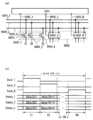
도 3은 표시 장치의 블록도를 설명하는 도면.
도 4는 신호선 구동 회로의 구성을 설명하는 도면 및 동작을 설명하는 타이밍 차트.
도 5는 구동 회로를 형성하는 시프트 레지스터 및 펄스 출력 회로를 설명하는 블록도.
도 6은 구동 회로를 형성하는 펄스 출력 회로를 설명하는 회로도.
도 7은 시프트 레지스터의 동작을 설명하는 타이밍 차트.
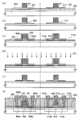
도 8은 구동 회로에 이용하는 보호 회로의 제작 방법을 설명하는 단면도.
도 9는 구동 회로에 이용하는 보호 회로의 제작 방법을 설명하는 단면도.
도 10은 구동 회로에 이용하는 보호 회로의 제작 방법을 설명하는 단면도.
도 11은 구동 회로에 이용하는 보호 회로의 제작 방법을 설명하는 단면도.
도 12는 구동 회로를 갖는 표시 장치를 설명하는 도면.
도 13은 구동 회로를 갖는 표시 장치를 설명하는 도면.
도 14는 개시하는 발명의 구동 회로를 이용한 표시 장치를 갖는 전자 기기의 외관도.
도 15는 구동 회로에 이용하는 보호 회로의 제작 방법을 설명하는 단면도.
도 16은 구동 회로에 이용하는 보호 회로를 설명하는 단면도.1 is a circuit diagram illustrating a protection circuit used for a drive circuit.
2 is a circuit diagram illustrating a protection circuit used for a drive circuit.
3 is a diagram for explaining a block diagram of a display device;
4 is a timing chart for explaining the configuration and operation of the signal line driver circuit.
5 is a block diagram illustrating a shift register and a pulse output circuit forming a drive circuit.
6 is a circuit diagram illustrating a pulse output circuit forming a drive circuit.
7 is a timing chart for explaining the operation of the shift register.
8 is a cross-sectional view illustrating a method of manufacturing a protection circuit used in a drive circuit.
9 is a cross-sectional view illustrating a method of manufacturing a protection circuit for use in a drive circuit.
10 is a cross-sectional view illustrating a method of manufacturing a protection circuit used in a drive circuit.
11 is a cross-sectional view illustrating a method of manufacturing a protection circuit used in a drive circuit.
12 illustrates a display device having a driving circuit.
13 illustrates a display device having a drive circuit.
14 is an external view of an electronic apparatus having a display device using the driving circuit of the disclosed invention.
15 is a cross-sectional view illustrating a method of manufacturing a protection circuit used in a drive circuit.
16 is a cross-sectional view illustrating a protection circuit used in a drive circuit.
본 발명의 실시 형태의 일례에 대해, 도면을 이용하여 이하에 설명한다. 단, 본 발명은 이하의 설명으로 한정되지 않고, 본 발명의 취지 및 그 범위로부터 일탈하는 일 없이 형태 및 상세를 다양하게 변경할 수 있는 것은 당업자라면 용이하게 이해된다. 따라서, 본 발명은 이하에 나타내는 실시 형태의 기재 내용으로 한정하여 해석되는 것은 아니다. 또한, 이하에 설명하는 실시 형태에 있어서, 동일 부분 또는 동일한 기능을 갖는 부분에는 동일한 부호를 다른 도면 사이에서 공통적으로 이용하고, 그 반복의 설명은 생략한다.An example of embodiment of this invention is demonstrated below using drawing. However, this invention is not limited to the following description, It is easily understood by those skilled in the art that various forms and details can be changed without deviating from the meaning and range of this invention. Therefore, this invention is not limited to the description content of embodiment shown below and is not interpreted. In addition, in embodiment described below, the same code | symbol is used common among different drawings for the same part or the part which has the same function, and the description of the repetition is abbreviate | omitted.
또한, 도면 등에 있어서 도시하는 각 구성의, 위치, 크기, 범위 등은 이해를 간단하게 하기 위해, 실제의 위치, 크기, 범위 등을 나타내고 있지 않은 경우가 있다. 이로 인해, 개시하는 발명은, 반드시, 도면 등에 개시된 위치, 크기, 범위 등으로 한정되지 않는다.In addition, the position, size, range, etc. of each structure shown in drawing etc. may not show actual position, size, range, etc. for simplicity of understanding. For this reason, the invention disclosed is not necessarily limited to the position, size, range, etc. which were disclosed in drawings or the like.
또한, 본 명세서 등에 있어서의 「제1」, 「제2」, 「제3」 등의 서수는 구성 요소의 혼동을 피하기 위해 부여하는 것으로, 수적으로 한정하는 것이 아님을 부기한다.Note that ordinal numbers such as "first", "second", "third", and the like in the present specification and the like are given to avoid confusion of components, and are not limited in number.
(실시 형태 1)(Embodiment 1)
본 실시 형태에서는, 개시하는 발명의 일 형태에 관한 구동 회로 및 구동 회로에 이용할 수 있는 보호 회로의 구성 및 동작 방법에 대해 도 1 내지 도 4를 이용하여 설명한다.In this embodiment, the structure and operation method of the protection circuit which can be used for the drive circuit and drive circuit which concern on one form of invention disclosed are demonstrated using FIGS.
개시하는 발명의 일 형태에 관한, 구동 회로에 이용하는 보호 회로와, 구동 회로를 구성하는 반도체 소자의 접속 관계를 도 1에 도시한다. 구동 회로는 구동 회로를 구성하는 반도체 소자(101)의 단자의 하나와 제1 배선(102) 사이에 제1 보호 회로(104)가 설치되고, 구동 회로를 구성하는 반도체 소자(101)의 단자의 하나와 제2 배선(103) 사이에 제2 보호 회로(105)가 설치되는 구성으로 되어 있다. 또한, 도 1에 도시하는 구동 회로에 있어서, 제1 배선(102)은 고전위 전원선(VDD), 제2 배선(103)은 저전위 전원선(VSS)으로 할 수 있다. 또한, 제2 배선(103)은 접지 전위선(GND)으로 해도 된다.1 shows a connection relationship between a protection circuit used for a drive circuit and a semiconductor element constituting the drive circuit according to one embodiment of the disclosed invention. The driving circuit is provided with a
도 1에 도시하는 구동 회로에 있어서는, 제1 보호 회로(104)로서 트랜지스터(114)가 설치되고, 제2 보호 회로(105)로서 트랜지스터(115)가 설치되고, 반도체 소자(101)로서 트랜지스터(111)가 설치되어 있다. 여기서, 트랜지스터(111)의 게이트 전극층과, 트랜지스터(114)의 소스 전극층 또는 드레인 전극층의 한쪽과, 트랜지스터(115)의 소스 전극층 또는 드레인 전극층의 한쪽이 전기적으로 접속된다. 또한, 트랜지스터(114)의 소스 전극층 또는 드레인 전극층의 다른 쪽과 제1 배선(102)이 전기적으로 접속되고, 트랜지스터(115)의 소스 전극층 또는 드레인 전극층의 다른 쪽과 제2 배선(103)이 전기적으로 접속된다. 또한, 트랜지스터(111)의 게이트 전극층의 전위가 제1 배선(102)의 전위보다 높은 경우에 순방향 바이어스로 되도록, 트랜지스터(114)의 게이트 전극층과 소스 전극층 또는 드레인 전극층의 어느 하나가 전기적으로 접속되고, 트랜지스터(111)의 게이트 전극층의 전위가 제2 배선(103)의 전위보다 낮은 경우에 순방향 바이어스로 되도록, 트랜지스터(115)의 게이트 전극층과 소스 전극층 또는 드레인 전극층의 어느 하나가 전기적으로 접속된다.In the driving circuit shown in FIG. 1, the
또한, 본 실시 형태에 있어서는, 트랜지스터(114) 및 트랜지스터(115)는 n채널형으로서 설명을 행하지만, 이에 한정되지 않고 p채널형으로 해도 된다. p채널형으로 하는 경우, 제1 배선(102)과 제2 배선(103)에 부여되는 전위를 반대로 한다.In addition, in this embodiment, although the
반도체 소자(101)는 트랜지스터로 한정되지 않고, 구동 회로를 형성하는 반도체 소자이면 어떤 소자라도 대상이 된다. 또한, 반도체 소자(101)의 단자로서는, 반도체 소자에 접속된 배선도 포함하는 것으로 한다. 또한, 구동 회로 내의 복수의 반도체 소자(101) 각각에 대해, 도 1에 도시한 바와 같이 제1 보호 회로(104) 및 제2 보호 회로(105)를 설치할 수도 있다.The
제1 보호 회로(104)는 제1 배선(102)과 반도체 소자(101)의 단자 사이에 인가되는 전압의 대소에 의해 순방향 바이어스 또는 역방향 바이어스를 취하는 비선형 소자를 형성하고 있으면 되고, 도 1에 도시하는 구동 회로에 있어서는, 게이트 전극층과 소스 전극층 또는 드레인 전극층의 어느 하나가 전기적으로 접속된 트랜지스터(114)로 하였다. 여기서, 트랜지스터(114)가 n채널형인 경우, 트랜지스터(114)의 게이트 전극층은 소스 전극층 또는 드레인 전극층의 한쪽(여기서는, 소스 전극층)과 전기적으로 접속된다.The
또한, 제1 보호 회로(104)는 적어도 하나 이상의, 게이트 전극층과 소스 전극층 또는 드레인 전극층의 어느 하나가 전기적으로 접속된 트랜지스터(114)를 갖고 있으면 되고, 다른 반도체 소자를 포함하고 있어도 된다. 예를 들어, 도 2에 도시한 바와 같이, 게이트 전극층과 소스 전극층 또는 드레인 전극층의 어느 하나가 전기적으로 접속된 트랜지스터(114a) 및 트랜지스터(114b)를 직렬로 접속하여 제1 보호 회로(104)를 형성해도 된다. 물론 3개 이상의 트랜지스터를 직렬로 접속해도 된다.In addition, the
제2 보호 회로(105)는 제2 배선(103)과 반도체 소자(101)의 단자 사이에 인가되는 전압의 대소에 의해 순방향 바이어스 또는 역방향 바이어스를 취하는 비선형 소자를 형성하고 있으면 되고, 도 1에 도시하는 구동 회로에 있어서는, 게이트 전극층과 소스 전극층 또는 드레인 전극층의 어느 하나가 전기적으로 접속된 트랜지스터(115)로 하였다. 여기서, 트랜지스터(115)가 n채널형인 경우, 트랜지스터(115)의 게이트 전극층은 소스 전극층 또는 드레인 전극층의 다른 쪽(여기서는, 소스 전극층)과 전기적으로 접속된다.The
또한, 제2 보호 회로(105)도 제1 보호 회로(104)와 마찬가지로, 적어도 하나 이상의, 게이트 전극층과 소스 전극층 또는 드레인 전극층의 어느 하나가 전기적으로 접속된 트랜지스터(115)를 갖고 있으면 되고, 다른 반도체 소자를 포함하고 있어도 된다. 예를 들어, 도 2에 도시한 바와 같이, 게이트 전극층과 소스 전극층 또는 드레인 전극층의 어느 하나가 전기적으로 접속된 트랜지스터(115a) 및 트랜지스터(115b)를 직렬로 접속하여 제2 보호 회로(105)를 형성해도 된다. 물론 3개 이상의 트랜지스터를 직렬로 접속해도 된다.In addition, similarly to the
여기서, 트랜지스터(114) 및 트랜지스터(115)는 역방향 바이어스가 인가될 때의 오프 전류가 극히 작은 것이 바람직하다. 오프 전류가 극히 작은 트랜지스터로서는, 실리콘보다도 넓은 밴드 갭을 갖는 반도체(와이드 밴드 갭 반도체)를 채널 형성 영역에 이용한 트랜지스터를 예로 들 수 있다.Here, it is preferable that the
구체적으로는, 매우 높은 오프 저항을 얻기 위해서는, 실리콘(밴드 갭 1.1eV)에서는 불충분하고, 밴드 갭이 2.5eV 이상 4eV 이하, 바람직하게는 3eV 이상 3.8eV 이하의 와이드 밴드 갭 반도체를 이용하면 된다. 와이드 밴드 갭 반도체의 일례로서, 탄화규소(SiC), 질화갈륨(GaN) 등의 화합물 반도체, In-Ga-Zn-O계 산화물 반도체 등의 금속 산화물로 이루어지는 산화물 반도체 등을 적용할 수 있다.Specifically, in order to obtain a very high off resistance, it is insufficient in silicon (band gap 1.1 eV), and a wide band gap semiconductor having a band gap of 2.5 eV or more and 4 eV or less, preferably 3 eV or more and 3.8 eV or less may be used. As an example of a wide band gap semiconductor, an oxide semiconductor made of a compound semiconductor such as silicon carbide (SiC), gallium nitride (GaN), or a metal oxide such as an In—Ga—Zn—O-based oxide semiconductor may be used.
트랜지스터의 오프 저항은 채널이 형성되는 반도체층에 있어서, 열적으로 여기되는 캐리어의 농도에 반비례한다. 도너나 억셉터에 의한 캐리어가 전혀 존재하지 않는 상태(진성 반도체)라도, 실리콘의 경우에는 밴드 갭이 1.1eV이므로, 실온 300K에서의 열여기 캐리어의 농도는 1×10¹¹㎝-3 정도이다.The off resistance of the transistor is inversely proportional to the concentration of the thermally excited carrier in the semiconductor layer in which the channel is formed. Even in a state where no carriers due to donors or acceptors exist (intrinsic semiconductors), since the band gap is 1.1 eV in the case of silicon, the concentration of the heat-excited carrier at room temperature 300K is about 1 x 1011 cm-3 .
한편, 밴드 갭 3.2eV의 와이드 밴드 갭 반도체에서는 열여기 캐리어의 농도는 1×10⁻⁷㎝-3 정도가 된다. 전자 이동도가 동일한 경우, 오프 저항은 캐리어 농도에 반비례하므로, 밴드 갭 3.2eV의 반도체의 오프 저항은 실리콘보다 18자리나 커진다. 이와 같은 화합물 반도체로서는, 예를 들어 In-Ga-Zn-O계나 In-Sn-Zn-O계의 산화물 반도체가 알려져 있다.On the other hand, in a wide band gap semiconductor having a band gap of 3.2 eV, the concentration of the heat-excited carrier is about 1 × 10⁻⁷ cm−3 . When the electron mobility is the same, the off resistance is inversely proportional to the carrier concentration, so that the off resistance of the semiconductor having a band gap of 3.2 eV is 18 orders of magnitude larger than that of silicon. As such a compound semiconductor, for example, an In-Ga-Zn-O-based or In-Sn-Zn-O-based oxide semiconductor is known.
따라서, 트랜지스터(114) 및 트랜지스터(115)에 산화물 반도체로 대표되는 와이드 밴드 갭 반도체를 이용하면, 역방향 바이어스가 인가될 때의 오프 전류를 극히 작게 할 수 있다. 또한, 구동 회로를 형성하는 트랜지스터(111)도 마찬가지로, 산화물 반도체로 대표되는 와이드 밴드 갭 반도체를 이용하는 것이 바람직하다. 이에 의해, 트랜지스터(111)의 오프 전류를 저감시켜, 구동 회로의 소비 전력의 저감을 도모할 수 있다.Therefore, when wide band gap semiconductors represented by oxide semiconductors are used for the
상술한 바와 같이 구동 회로에 있어서, 제1 보호 회로(104) 및 제2 보호 회로(105)를, 구동 회로를 형성하는 반도체 소자(101)의 단자의 하나에 접속함으로써, ESD 등의 높은 서지 전압이 반도체 소자(101)의 단자의 하나에 인가된 경우라도, 제1 보호 회로(104) 또는 제2 보호 회로(105)가 방전 경로가 되어, 서지 전류가 반도체 소자(101)에 흐르는 것을 방지할 수 있다.As described above, in the driving circuit, by connecting the
예를 들어, 플러스의 서지 전압이 반도체 소자(101)의 단자의 하나에 인가된 경우, 제1 보호 회로(104)가 순방향 바이어스로 되므로, 반도체 소자(101)의 단자의 하나로부터 제1 배선(102)으로 전류가 흐른다. 또한, 마이너스의 서지 전압이 반도체 소자(101)의 단자의 하나에 인가된 경우, 제2 보호 회로(105)가 순방향 바이어스로 되므로, 제2 배선(103)으로부터 반도체 소자(101)의 단자의 하나로 전류가 흐른다. 이와 같이 하여 ESD 등에서 반도체 소자(101)의 단자의 하나에 공급된 전하를 상쇄하여, 반도체 소자(101)로의 불필요한 전하의 유입을 방지할 수 있다. 특히 반도체 소자(101)로서 트랜지스터(111)를 이용하는 경우, 제1 보호 회로(104) 및 제2 보호 회로(105)가 없으면, 서지 전압에 의해 과잉의 전류가 트랜지스터(111)의 게이트 절연막을 통과하여 트랜지스터(111)가 절연 파괴를 일으킬 우려가 있지만, 제1 보호 회로(104) 및 제2 보호 회로(105)를 설치함으로써 그 위험성을 배제할 수 있다.For example, when a positive surge voltage is applied to one of the terminals of the
또한, 상술한 제1 보호 회로(104) 및 제2 보호 회로(105)의 기능은 제1 배선(102)에 고전위가 부여되고, 제2 배선(103)에 저전위가 부여되는 경우뿐만 아니라, 제1 배선(102) 및 제2 배선(103)에 이들의 전위가 부여되어 있지 않은 경우, 즉 구동 회로의 제작 공정의 도중, 혹은 구동 회로를 표시 장치에 설치하고 있는 도중에 대해서도 마찬가지라고 할 수 있다. 플러스의 서지 전압은 전압의 절대값이 충분히 크기 때문에, 제1 배선(102)에 고전위가 부여되어 있지 않아도 제1 보호 회로(104)는 순방향 바이어스로 된다. 또한, 마이너스의 서지 전압도 전압의 절대값이 충분히 크기 때문에, 제2 배선(103)에 저전위가 부여되어 있지 않아도 제2 보호 회로(105)는 순방향 바이어스로 된다.In addition, the functions of the first
단, 구동 회로의 제작 공정의 도중에 있어서, 제1 보호 회로(104) 및 제2 보호 회로(105)를 동작시키기 위해서는, 제1 보호 회로(104) 및 제2 보호 회로(105)와 반도체 소자(101)를 동시에 제작하는 것이 필요하다. 따라서, 트랜지스터(114), 트랜지스터(115) 및 트랜지스터(111)는 동일한 구성으로 동시에 제작하는 것이 바람직하다.However, in order to operate the
또한, 구동 회로의 통상 동작 시에 있어서는, 제1 보호 회로(104) 또는 제2 보호 회로(105)에 이용되는 트랜지스터(114) 또는 트랜지스터(115)가 역방향 바이어스 상태이거나, 또는 제1 배선(102) 또는 제2 배선(103)과 반도체 소자(101)의 단자의 하나 사이의 전위차가 트랜지스터(114) 또는 트랜지스터(115)의 동작 전압을 초과하지 않는 상태이므로, 제1 보호 회로(104) 또는 제2 보호 회로(105)는 기본적으로는 동작하지 않는다.In the normal operation of the drive circuit, the
이때, 트랜지스터(114) 및 트랜지스터(115)에 실리콘 등의 밴드 갭이 좁은 반도체를 이용하면, 역방향 바이어스에서도 약간의 전류가 흐르기 때문에, 제1 배선(102) 또는 제2 배선(103)과 반도체 소자(101)의 단자의 하나 사이에서 리크 전류가 흘러, 제1 배선(102) 또는 제2 배선(103)의 전위, 또는 반도체 소자(101)의 단자의 하나의 전위에 변화가 발생해 버린다.In this case, when a semiconductor having a narrow band gap such as silicon is used for the
그러나, 상술한 바와 같이 트랜지스터(114) 및 트랜지스터(115)에 산화물 반도체로 대표되는 와이드 밴드 갭 반도체를 이용함으로써, 역방향 바이어스가 인가될 때의 트랜지스터(114) 및 트랜지스터(115)의 오프 전류를 극히 작게 할 수 있으므로, 제1 보호 회로(104) 및 제2 보호 회로(105)의 리크 전류를 저감시킬 수 있다.However, by using the wide band gap semiconductor represented by the oxide semiconductor for the
또한, 도 2에 도시한 바와 같이, 트랜지스터(114) 또는 트랜지스터(115)를 직렬로 접속하고, 제1 보호 회로(104) 또는 제2 보호 회로(105)를 형성함으로써, 제1 보호 회로(104) 또는 제2 보호 회로(105)에 순방향 바이어스가 걸려 전류가 흐르기 위해 필요한, 반도체 소자(101)의 단자의 하나와 제1 배선(102)의 전위차, 또는 반도체 소자(101)의 단자의 하나와 제2 배선(103)의 전위차를 크게 할 수 있다. 예를 들어, 트랜지스터(114)가 n개 직렬로 접속되어 있는 경우에는, 반도체 소자(101)의 단자의 하나와 제1 배선(102)의 전위차가 n×Vth[Vth는 트랜지스터(114)의 임계값 전압] 이상으로 되지 않으면, 제1 보호 회로(104)에 순방향 바이어스의 전류는 흐르지 않는다. 따라서, 소량의 노이즈 등이 반도체 소자(101)의 단자에 들어감으로써 제1 보호 회로(104) 또는 제2 보호 회로(105)가 동작해 버리는 것을 방지할 수 있다.As shown in FIG. 2, the
도 1 또는 도 2에 도시하는 보호 회로를 이용할 수 있는 구동 회로 및 구동 회로를 이용한 액티브 매트릭스 표시 장치의 일례를 이하에 나타낸다.An example of the active matrix display device using the drive circuit and drive circuit which can use the protection circuit shown in FIG. 1 or FIG. 2 is shown below.
액티브 매트릭스형 표시 장치의 블록도의 일례를 도 3의 (a)에 도시한다. 표시 장치의 기판(5300) 위에는 화소부(5301), 제1 주사선 구동 회로(5302), 제2 주사선 구동 회로(5303), 신호선 구동 회로(5304)가 설치된다. 화소부(5301)에는 복수의 신호선이 신호선 구동 회로(5304)로부터 연신하여 배치되고, 복수의 주사선이 제1 주사선 구동 회로(5302) 및 제2 주사선 구동 회로(5303)로부터 연신하여 배치되어 있다. 또한 주사선과 신호선의 교차 영역에는, 각각, 표시 소자를 갖는 화소가 매트릭스 형상으로 배치되어 있다. 또한, 표시 장치의 기판(5300)은 FPC(Flexible Printed Circuit) 등의 접속부를 통해, 타이밍 제어 회로(5305)(컨트롤러, 제어 IC라고도 함)에 접속되어 있다.An example of a block diagram of an active matrix display device is shown in Fig. 3A. The
도 3의 (a)에 도시하는, 제1 주사선 구동 회로(5302), 제2 주사선 구동 회로(5303), 신호선 구동 회로(5304)에는 도 1 또는 도 2에서 도시한 구동 회로를 이용할 수 있다. 또한, 제1 주사선 구동 회로(5302), 제2 주사선 구동 회로(5303), 신호선 구동 회로(5304)는 화소부(5301)와 동일한 기판(5300) 위에 형성된다. 그로 인해, 외부에 설치하는 구동 회로 등의 부품의 수가 줄기 때문에, 비용의 저감을 도모할 수 있다. 또한, 기판(5300)과 외부의 구동 회로의 접속부(FPC 등)를 줄일 수 있으므로, 신뢰성의 향상, 또는 수율의 향상을 도모할 수 있다.The drive circuit shown in FIG. 1 or 2 can be used for the 1st scan
또한, 타이밍 제어 회로(5305)는 제1 주사선 구동 회로(5302)에 대해, 일례로서, 제1 주사선 구동 회로용 스타트 신호(GSP1), 주사선 구동 회로용 클록 신호(GCK1)를 공급한다. 또한, 타이밍 제어 회로(5305)는 제2 주사선 구동 회로(5303)에 대해, 일례로서, 제2 주사선 구동 회로용 스타트 신호(GSP2)(스타트 펄스라고도 함), 주사선 구동 회로용 클록 신호(GCK2)를 공급한다. 신호선 구동 회로(5304)에, 신호선 구동 회로용 스타트 신호(SSP), 신호선 구동 회로용 클록 신호(SCK), 비디오 신호용 데이터(DATA)(단순히 비디오 신호라고도 함), 래치 신호(LAT)를 공급하는 것으로 한다. 또한 각 클록 신호는 주기가 어긋난 복수의 클록 신호여도 되고, 클록 신호를 반전시킨 신호(CKB)와 함께 공급되는 것이어도 된다. 또한, 제1 주사선 구동 회로(5302)와 제2 주사선 구동 회로(5303)의 한쪽을 생략하는 것이 가능하다.In addition, the
도 3의 (b)에서는 구동 주파수가 낮은 회로[예를 들어, 제1 주사선 구동 회로(5302), 제2 주사선 구동 회로(5303)]를 화소부(5301)와 동일한 기판(5300)에 형성하고, 신호선 구동 회로(5304)를 화소부(5301)와는 다른 기판에 형성하는 구성에 대해 도시하고 있다. 그 구성에 의해, 단결정 반도체를 이용한 트랜지스터와 비교하면 전계 효과 이동도가 작은 박막 트랜지스터에 의해, 기판(5300)에 형성하는 구동 회로를 구성할 수 있다. 따라서, 표시 장치의 대형화, 공정수의 삭감, 비용의 저감, 또는 수율의 향상 등을 도모할 수 있다.In FIG. 3B, a circuit having a low driving frequency (for example, a first scan
또한, 도 3의 (a) 및 도 3의 (b)에 도시하는, 제1 주사선 구동 회로(5302), 제2 주사선 구동 회로(5303) 또는 신호선 구동 회로(5304) 및 구동 회로의 일부는 LSI로 형성해도 된다.3A and 3B, the first scan
또한, 도 4의 (a), 도 4의 (b)에서는 n채널형 TFT로 구성하는 신호선 구동 회로의 구성, 동작에 대해 일례를 나타내어 설명한다.4A and 4B, an example of the configuration and operation of the signal line driver circuit constituted by the n-channel TFT will be described.
신호선 구동 회로는 시프트 레지스터(5601) 및 스위칭 회로(5602)를 갖는다. 스위칭 회로(5602)는 스위칭 회로(5602_1 내지 5602_N)(N은 자연수)라고 하는 복수의 회로를 갖는다. 스위칭 회로(5602_1 내지 5602_N)는, 각각, 박막 트랜지스터(5603_1 내지 5603_k)(k은 자연수)라고 하는 복수의 트랜지스터를 갖는다. 박막 트랜지스터(5603_1 내지 5603_k)는 n채널형 TFT인 예를 설명한다.The signal line driver circuit has a
신호선 구동 회로의 접속 관계에 대해, 스위칭 회로(5602_1)를 예로 들어 설명한다. 박막 트랜지스터(5603_1 내지 5603_k)의 제1 단자는, 각각, 배선(5604_1 내지 5604_k)과 접속된다. 박막 트랜지스터(5603_1 내지 5603_k)의 제2 단자는, 각각, 신호선 S1 내지 Sk와 접속된다. 박막 트랜지스터(5603_1 내지 5603_k)의 게이트는 배선(5605_1)과 접속된다.The connection relationship between the signal line driver circuits will be described using the switching circuit 5602_1 as an example. The first terminals of the thin film transistors 5603_1 to 5603_k are connected to the wirings 5560_1 to 5604_k, respectively. The second terminals of the thin film transistors 5603_1 to 5603_k are connected to the signal lines S1 to Sk, respectively. Gates of the thin film transistors 5603_1 to 5603_k are connected to a wiring 5405_1.
시프트 레지스터(5601)는 배선(5605_1 내지 5605_N)에 순서대로 H레벨(H신호, 고전원 전위 레벨이라고도 함)의 신호를 출력하여, 스위칭 회로(5602_1 내지 5602_N)를 순서대로 선택하는 기능을 갖는다.The
예를 들어, 스위칭 회로(5602_1)는 배선(5604_1 내지 5604_k)과 신호선 S1 내지 Sk의 도통 상태(제1 단자와 제2 단자 사이의 도통)을 제어하는 기능, 즉 배선(5604_1 내지 5604_k)의 전위를 신호선 S1 내지 Sk에 공급할지 여부를 제어하는 기능을 갖는다. 이와 같이, 스위칭 회로(5602_1)는 셀렉터로서의 기능을 갖는다. 또한 박막 트랜지스터(5603_1 내지 5603_k)는, 각각, 배선(5604_1 내지 5604_k)과 신호선 S1 내지 Sk의 도통 상태를 제어하는 기능, 즉 배선(5604_1 내지 5604_k)의 전위를 신호선 S1 내지 Sk에 공급하는 기능을 갖는다. 이와 같이, 박막 트랜지스터(5603_1 내지 5603_k)는, 각각, 스위치로서의 기능을 갖는다.For example, the switching circuit 5602_1 has a function of controlling the conduction state (conduction between the first terminal and the second terminal) of the wirings 5604_1 to 5604_k and the signal lines S1 to Sk, that is, the potential of the wirings 5604_1 to 5604_k. Has a function of controlling whether or not to be supplied to the signal lines S1 to Sk. In this way, the switching circuit 5602_1 has a function as a selector. Further, the thin film transistors 5603_1 to 5603_k each have a function of controlling the conduction state of the wirings 5604_1 to 5604_k and the signal lines S1 to Sk, that is, to supply the potentials of the wirings 5560_1 to 5604_k to the signal lines S1 to Sk, respectively. Have As described above, the thin film transistors 5603_1 to 5603_k each have a function as a switch.
또한, 배선(5604_1 내지 5604_k)에는, 각각, 비디오 신호용 데이터(DATA)가 입력된다. 비디오 신호용 데이터(DATA)는 화상 정보 또는 화상 신호에 따른 아날로그 신호인 경우가 많다.The data DATA for video signal is input to the wirings 5560_1 to 5604_k, respectively. The video signal data DATA is often an analog signal corresponding to picture information or picture signals.
다음에, 도 4의 (a)의 신호선 구동 회로의 동작에 대해, 도 4의 (b)의 타이밍 차트를 참조하여 설명한다. 도 4의 (b)에는 신호 Sout_1 내지 Sout_N 및 신호 Vdata_1 내지 Vdata_k의 일례를 나타낸다. 신호 Sout_1 내지 Sout_N는, 각각, 시프트 레지스터(5601)의 출력 신호의 일례이고, 신호 Vdata_1 내지 Vdata_k는, 각각, 배선(5604_1 내지 5604_k)에 입력되는 신호의 일례이다. 또한, 신호선 구동 회로의 1 동작 기간은, 표시 장치에 있어서의 1 게이트 선택 기간에 대응한다. 1 게이트 선택 기간은, 일례로서, 기간 T1 내지 기간 TN으로 분할된다. 기간 T1 내지 TN은, 각각, 선택된 행에 속하는 화소에 비디오 신호용 데이터(DATA)를 기입하기 위한 기간이다.Next, the operation of the signal line driver circuit of FIG. 4A will be described with reference to the timing chart of FIG. 4B. 4B shows an example of the signals Sout_1 to Sout_N and the signals Vdata_1 to Vdata_k. The signals Sout_1 to Sout_N are examples of output signals of the
또한, 본 실시 형태의 도면 등에 있어서 도시하는 각 구성의, 신호 파형의 밸브 등은 명료화를 위해 과장하여 표기하고 있는 경우가 있다. 따라서, 반드시 그 스케일로 한정되지 않는 것인 것을 부기한다.In addition, the valve etc. of the signal waveform of each structure shown in the figure etc. of this embodiment may be exaggerated and shown for clarity. Therefore, it adds that it is not necessarily limited to the scale.
기간 T1 내지 기간 TN에 있어서, 시프트 레지스터(5601)는 H레벨의 신호를 배선(5605_1 내지 5605_N)에 순서대로 출력한다. 예를 들어, 기간 T1에 있어서, 시프트 레지스터(5601)는 하이 레벨의 신호를 배선(5605_1)에 출력한다. 그러면, 박막 트랜지스터(5603_1 내지 5603_k)는 온으로 되므로, 배선(5604_1 내지 5604_k)과, 신호선 S1 내지 Sk가 도통 상태로 된다. 이때, 배선(5604_1 내지 5604_k)에는 Data(S1) 내지 Data(Sk)가 입력된다. Data(S1) 내지 Data(Sk)는, 각각, 박막 트랜지스터(5603_1 내지 5603_k)를 통해, 선택되는 행에 속하는 화소 중, 1열째 내지 k열째의 화소에 기입된다. 이와 같이 하여, 기간 T1 내지 TN에 있어서, 선택된 행에 속하는 화소에, k열씩 순서대로 비디오 신호용 데이터(DATA)가 기입된다.In the period T1 to the period TN, the
이상과 같이, 비디오 신호용 데이터(DATA)가 복수의 열씩 화소에 기입됨으로써, 비디오 신호용 데이터(DATA)의 수, 또는 배선의 수를 줄일 수 있다. 따라서, 외부 회로와의 접속수를 줄일 수 있다. 또한, 비디오 신호용 데이터(DATA)가 복수의 열씩 화소에 기입됨으로써, 기입 시간을 길게 할 수 있어, 비디오 신호용 데이터(DATA)의 기입 부족을 방지할 수 있다.As described above, the video signal data DATA is written to the pixels in a plurality of columns so that the number of data signals DATA or the number of wirings can be reduced. Therefore, the number of connections with an external circuit can be reduced. In addition, by writing the video signal data DATA to the pixels in a plurality of columns, the writing time can be lengthened, and the shortage of writing of the video signal data DATA can be prevented.
주사선 구동 회로 및/또는 신호선 구동 회로의 일부에 이용할 수 있고, 도 1 또는 도 2에 도시하는 보호 회로를 이용한 시프트 레지스터의 일 형태에 대해 도 5 내지 도 7을 이용하여 설명한다.One form of the shift register using the protection circuit shown in FIG. 1 or 2, which can be used for a part of the scan line driver circuit and / or the signal line driver circuit, will be described with reference to FIGS.
주사선 구동 회로는 시프트 레지스터를 갖고 있다. 또한 경우에 따라서는 레벨 시프터나 버퍼 등을 갖고 있어도 된다. 주사선 구동 회로에 있어서, 시프트 레지스터에 클록 신호(CK) 및 스타트 펄스 신호(SP)가 입력됨으로써, 선택 신호가 생성된다. 생성된 선택 신호는 버퍼에 있어서 완충 증폭되고, 대응하는 주사선에 공급된다. 주사선에는 1 라인분의 화소의 트랜지스터의 게이트 전극이 접속되어 있다. 그리고, 1 라인 분의 화소의 트랜지스터를 일제히 ON으로 해야만 하므로, 버퍼는 큰 전류를 흘리는 것이 가능한 것이 이용된다.The scan line driver circuit has a shift register. In some cases, the present invention may have a level shifter, a buffer, or the like. In the scan line driver circuit, the clock signal CK and the start pulse signal SP are input to the shift register, whereby a selection signal is generated. The generated selection signal is buffered and amplified in the buffer and supplied to the corresponding scan line. Gate electrodes of transistors of pixels for one line are connected to the scan line. Since the transistors of one line of pixels must all be turned ON at the same time, a buffer capable of flowing a large current is used.
시프트 레지스터는 제1 펄스 출력 회로(10_1) 내지 제N 펄스 출력 회로(10_N)(N은 3 이상의 자연수)를 갖고 있다[도 5의 (a) 참조]. 도 5의 (a)에 도시하는 시프트 레지스터의 제1 펄스 출력 회로(10_1) 내지 제N 펄스 출력 회로(10_N)에는 제1 배선(11)으로부터 제1 클록 신호(CK1), 제2 배선(12)으로부터 제2 클록 신호(CK2), 제3 배선(13)으로부터 제3 클록 신호(CK3), 제4 배선(14)으로부터 제4 클록 신호(CK4)가 공급된다. 또한 제1 펄스 출력 회로(10_1)에서는 제5 배선(15)으로부터의 스타트 펄스(SP1)(제1 스타트 펄스)가 입력된다. 또한 2단째 이후의 제n 펄스 출력 회로(10_n)(n은 2 이상, N 이하의 자연수)에서는, 1단 전단의 펄스 출력 회로로부터의 신호[전단 신호 OUT(n-1)이라고 함](n은 2 이상의 자연수)가 입력된다. 또한 제1 펄스 출력 회로(10_1)에서는 2단 후단의 제3 펄스 출력 회로(10_3)로부터의 신호가 입력된다. 마찬가지로, 2단째 이후의 제n 펄스 출력 회로(10_n)에서는, 2단 후단의 제(n+2) 펄스 출력 회로[10_(n+2)]로부터의 신호[후단 신호 OUT(n+2)이라고 함]가 입력된다. 따라서, 각 단의 펄스 출력 회로로부터는, 후단 및/또는 2개 전단의 펄스 출력 회로에 입력하기 위한 제1 출력 신호[OUT(1)(SR) 내지 OUT(N)(SR)], 다른 배선 등에 입력되는 제2 출력 신호[OUT(1) 내지 OUT(N)]가 출력된다. 또한, 도 5의 (a)에 도시한 바와 같이, 시프트 레지스터의 최종단의 2개의 단에는 후단 신호 OUT(n+2)가 입력되지 않지만, 일례로서는, 별도 제6 배선(16)으로부터 제2 스타트 펄스(SP2), 제7 배선(17)으로부터 제3 스타트 펄스(SP3)를 각각 입력하는 구성으로 하면 된다. 또는, 별도 시프트 레지스터의 내부에서 생성된 신호여도 된다. 예를 들어, 화소부로의 펄스 출력에 기여하지 않는 제(N+1) 펄스 출력 회로[10_(N+1)], 제(N+2) 펄스 출력 회로[10_(N+2)]를 설치하고(더미단이라고도 함), 더미단으로부터 제2 스타트 펄스(SP2) 및 제3 스타트 펄스(SP3)에 상당하는 신호를 생성하는 구성으로 해도 된다.The shift register has first pulse output circuits 10_1 to Nth pulse output circuits 10_N (N is a natural number of 3 or more) (see Fig. 5A). The first clock signal CK1 and the
또한, 클록 신호(CK)는 일정한 간격으로 H레벨과 L레벨(L신호, 저전원 전위 레벨이라고도 함)을 반복하는 신호이다. 여기서, 제1 클록 신호(CK1) 내지 제4 클록 신호(CK4)는, 순서대로 1/4 주기분 지연되어 있다. 본 실시 형태에서는, 제1 클록 신호(CK1) 내지 제4 클록 신호(CK4)를 이용하여, 펄스 출력 회로의 구동의 제어 등을 행한다. 또한, 클록 신호는 입력되는 구동 회로에 따라서, GCK, SCK라고 하는 경우도 있지만, 여기서는 CK로서 설명을 행한다.The clock signal CK is a signal which repeats H level and L level (L signal, also referred to as low power supply potential level) at regular intervals. Here, the first clock signal CK1 to the fourth clock signal CK4 are delayed by a quarter cycle in order. In the present embodiment, the drive of the pulse output circuit is controlled using the first clock signals CK1 to CK4. In addition, although a clock signal may be called GCK and SCK according to the input drive circuit, it demonstrates as CK here.
제1 입력 단자(21), 제2 입력 단자(22) 및 제3 입력 단자(23)는 제1 배선(11) 내지 제4 배선(14) 중 어느 하나와 전기적으로 접속되어 있다. 예를 들어, 도 5의 (a)에 있어서, 제1 펄스 출력 회로(10_1)는 제1 입력 단자(21)가 제1 배선(11)과 전기적으로 접속되고, 제2 입력 단자(22)가 제2 배선(12)과 전기적으로 접속되고, 제3 입력 단자(23)가 제3 배선(13)과 전기적으로 접속되어 있다. 또한, 제2 펄스 출력 회로(10_2)는 제1 입력 단자(21)가 제2 배선(12)과 전기적으로 접속되고, 제2 입력 단자(22)가 제3 배선(13)과 전기적으로 접속되고, 제3 입력 단자(23)가 제4 배선(14)과 전기적으로 접속되어 있다.The
제1 펄스 출력 회로(10_1) 내지 제N 펄스 출력 회로(10_N)의 각각은 제1 입력 단자(21), 제2 입력 단자(22), 제3 입력 단자(23), 제4 입력 단자(24), 제5 입력 단자(25), 제1 출력 단자(26), 제2 출력 단자(27)를 갖고 있는 것으로 한다[도 5의 (b) 참조]. 제1 펄스 출력 회로(10_1)에 있어서, 제1 입력 단자(21)에 제1 클록 신호(CK1)가 입력되고, 제2 입력 단자(22)에 제2 클록 신호(CK2)가 입력되고, 제3 입력 단자(23)에 제3 클록 신호(CK3)가 입력되고, 제4 입력 단자(24)에 스타트 펄스가 입력되고, 제5 입력 단자(25)에 후단 신호 OUT(3)이 입력되고, 제1 출력 단자(26)로부터 제1 출력 신호 OUT(1)(SR)이 출력되고, 제2 출력 단자(27)로부터 제2 출력 신호 OUT(1)이 출력되어 있게 된다.Each of the first pulse output circuits 10_1 to N-th pulse output circuit 10_N includes a
다음에, 도 5의 (a)에 도시한 펄스 출력 회로에 도 1 또는 도 2에 도시하는 보호 회로를 이용한 구체적인 회로 구성의 일례에 대해, 도 6을 이용하여 설명한다.Next, an example of a specific circuit configuration using the protection circuit shown in FIG. 1 or 2 in the pulse output circuit shown in FIG. 5A will be described with reference to FIG. 6.
도 6에 도시하는 펄스 출력 회로는 제1 트랜지스터(31) 내지 제11 트랜지스터(41)를 갖고 있다. 또한, 제1 보호 회로(104a) 내지 제1 보호 회로(104h), 제2 보호 회로(105a) 내지 제2 보호 회로(105h)를 갖고 있다. 여기서, 제1 보호 회로(104a) 내지 제1 보호 회로(104h)는 도 1 또는 도 2에 도시하는 제1 보호 회로(104)와 대응하고 있고, 제2 보호 회로(105a) 내지 제2 보호 회로(105h)는 도 1 또는 도 2에 도시하는 제2 보호 회로(105)와 대응하고 있다. 또한, 상술한 제1 입력 단자(21) 내지 제5 입력 단자(25) 및 제1 출력 단자(26), 제2 출력 단자(27)에 추가하여, 제1 고전원 전위 VDD가 공급되는 전원선(51), 저전원 전위 VSS가 공급되는 전원선(53)으로부터, 제1 트랜지스터(31) 내지 제11 트랜지스터(41)에 신호, 또는 전원 전위가 공급된다. 여기서 도 6에 있어서의 각 전원선의 전원 전위의 대소 관계는, 전원 전위 VDD는 전원 전위 VSS보다 큰 전위로 한다. 또한, 제1 클록 신호(CK1) 내지 제4 클록 신호(CK4)는 일정한 간격으로 H레벨과 L레벨을 반복하는 신호이지만, H레벨일 때에는 VDD, L레벨일 때에는 VSS라고 한다. 또한, 전원 전위 VDD보다 작고, 전원 전위 VSS보다 큰 전원 전위 VCC를 갖는 전원선을 설치해도 된다. 전원선의 전위 VCC를, 전원선(51)의 전위 VDD보다 낮게 함으로써, 동작에 영향을 미치는 일 없이, 트랜지스터의 게이트 전극에 인가되는 전위를 낮게 억제할 수 있고, 트랜지스터의 임계값의 시프트를 저감시켜, 열화를 억제할 수 있다.The pulse output circuit shown in FIG. 6 includes the
또한, 트랜지스터의 소스와 드레인은 박막 트랜지스터의 구조나 동작 조건 등에 따라서 바뀌기 때문에, 어느 것이 소스 또는 드레인인지를 한정하는 것이 곤란하다. 따라서, 소스 및 드레인으로서 기능하는 영역을, 소스 혹은 드레인이라고 부르지 않는 경우가 있다. 그 경우, 일례로서는, 각각을 제1 단자, 제2 단자로 표기하는 경우가 있다.In addition, since the source and the drain of the transistor change depending on the structure, the operating conditions, and the like of the thin film transistor, it is difficult to limit which is the source or the drain. Therefore, the area | region which functions as a source and a drain may not be called a source or a drain. In that case, as an example, each may be described as a 1st terminal and a 2nd terminal.
도 6에 있어서 제1 트랜지스터(31)는 제1 단자가 전원선(51)에 전기적으로 접속되고, 제2 단자가 제9 트랜지스터(39)의 제1 단자에 전기적으로 접속되고, 게이트 전극이 제4 입력 단자(24)에 전기적으로 접속되어 있다. 제2 트랜지스터(32)는 제1 단자가 전원선(53)에 전기적으로 접속되고, 제2 단자가 제9 트랜지스터(39)의 제1 단자에 전기적으로 접속되고, 게이트 전극이 제4 트랜지스터(34)의 게이트 전극에 전기적으로 접속되어 있다. 제3 트랜지스터(33)는 제1 단자가 제1 입력 단자(21)에 전기적으로 접속되고, 제2 단자가 제1 출력 단자(26)에 전기적으로 접속되어 있다. 제4 트랜지스터(34)는 제1 단자가 전원선(53)에 전기적으로 접속되고, 제2 단자가 제1 출력 단자(26)에 전기적으로 접속되어 있다. 제5 트랜지스터(35)는 제1 단자가 전원선(53)에 전기적으로 접속되고, 제2 단자가 제2 트랜지스터(32)의 게이트 전극 및 제4 트랜지스터(34)의 게이트 전극에 전기적으로 접속되고, 게이트 전극이 제4 입력 단자(24)에 전기적으로 접속되어 있다. 제6 트랜지스터(36)는 제1 단자가 전원선(51)에 전기적으로 접속되고, 제2 단자가 제2 트랜지스터(32)의 게이트 전극 및 제4 트랜지스터(34)의 게이트 전극에 전기적으로 접속되고, 게이트 전극이 제5 입력 단자(25)에 전기적으로 접속되어 있다. 제7 트랜지스터(37)는 제1 단자가 전원선(51)에 전기적으로 접속되고, 제2 단자가 제8 트랜지스터(38)의 제2 단자에 전기적으로 접속되고, 게이트 전극이 제3 입력 단자(23)에 전기적으로 접속되어 있다. 제8 트랜지스터(38)는 제1 단자가 제2 트랜지스터(32)의 게이트 전극 및 제4 트랜지스터(34)의 게이트 전극에 전기적으로 접속되고, 게이트 전극이 제2 입력 단자(22)에 전기적으로 접속되어 있다. 제9 트랜지스터(39)는 제1 단자가 제1 트랜지스터(31)의 제2 단자 및 제2 트랜지스터(32)의 제2 단자에 전기적으로 접속되고, 제2 단자가 제3 트랜지스터(33)의 게이트 전극 및 제10 트랜지스터(40)의 게이트 전극에 전기적으로 접속되고, 게이트 전극이 전원선(51)에 전기적으로 접속되어 있다. 제10 트랜지스터(40)는 제1 단자가 제1 입력 단자(21)에 전기적으로 접속되고, 제2 단자가 제2 출력 단자(27)에 전기적으로 접속되고, 게이트 전극이 제9 트랜지스터(39)의 제2 단자에 전기적으로 접속되어 있다. 제11 트랜지스터(41)는 제1 단자가 전원선(53)에 전기적으로 접속되고, 제2 단자가 제2 출력 단자(27)에 전기적으로 접속되고, 게이트 전극이 제2 트랜지스터(32)의 게이트 전극 및 제4 트랜지스터(34)의 게이트 전극에 전기적으로 접속되어 있다.In FIG. 6, in the
또한, 전원 전위 VCC를 갖는 전원선을 설치하는 경우, 제6 트랜지스터(36)의 제1 단자, 제7 트랜지스터(37)의 제1 단자 및 제9 트랜지스터(39)의 게이트 전극에 전원선(51) 대신에, 전원 전위 VCC를 갖는 전원선을 전기적으로 접속하면 된다.When a power supply line having a power supply potential VCC is provided, the
도 6에 있어서, 전원선(51)과 전기적으로 접속된 제1 보호 회로(104a)와 전원선(53)과 전기적으로 접속된 제2 보호 회로(105a) 사이에 제1 트랜지스터(31)의 게이트 전극이 전기적으로 접속되어 있다. 또한, 전원선(51)과 전기적으로 접속된 제1 보호 회로(104b)와 전원선(53)과 전기적으로 접속된 제2 보호 회로(105b) 사이에 제8 트랜지스터(38)의 게이트 전극이 전기적으로 접속되어 있다. 또한, 전원선(51)과 전기적으로 접속된 제1 보호 회로(104c)와 전원선(53)과 전기적으로 접속된 제2 보호 회로(105c) 사이에 제7 트랜지스터(37)의 게이트 전극이 전기적으로 접속되어 있다. 또한, 전원선(51)과 전기적으로 접속된 제1 보호 회로(104d)와 전원선(53)과 전기적으로 접속된 제2 보호 회로(105d) 사이에 제6 트랜지스터(36)의 게이트 전극이 전기적으로 접속되어 있다. 또한, 전원선(51)과 전기적으로 접속된 제1 보호 회로(104e)와 전원선(53)과 전기적으로 접속된 제2 보호 회로(105e) 사이에 제4 트랜지스터(34)의 게이트 전극이 전기적으로 접속되어 있다. 또한, 전원선(51)과 전기적으로 접속된 제1 보호 회로(104f)와 전원선(53)과 전기적으로 접속된 제2 보호 회로(105f) 사이에 제1 출력 단자(26)가 전기적으로 접속되어 있다. 또한, 전원선(51)과 전기적으로 접속된 제1 보호 회로(104g)와 전원선(53)과 전기적으로 접속된 제2 보호 회로(105g) 사이에 제1 입력 단자(21)가 전기적으로 접속되어 있다. 또한, 전원선(51)과 전기적으로 접속된 제1 보호 회로(104h)와 전원선(53)과 전기적으로 접속된 제2 보호 회로(105h) 사이에 제2 출력 단자(27)가 전기적으로 접속되어 있다.In FIG. 6, the gate of the
도 1 및 도 2를 이용하여 설명한 바와 같이, 전원선(51)과 접속된 제1 보호 회로(104a) 내지 제1 보호 회로(104h)와 전원선(53)과 접속된 제2 보호 회로(105a) 내지 제2 보호 회로(105h) 사이에 설치된 전극 또는 단자를 갖는 반도체 소자 및 전극이나 단자와 접속된 반도체 소자에 있어서, ESD 등의 높은 서지 전압이 인가된 경우라도, 제1 보호 회로(104a) 내지 제1 보호 회로(104h) 또는 제2 보호 회로(105a) 내지 제2 보호 회로(105h)가 방전 경로가 되어, 반도체 소자에 서지 전류가 흐르는 것을 방지할 수 있다.As described with reference to FIGS. 1 and 2, the
단, 제1 보호 회로(104a) 내지 제1 보호 회로(104h) 및 제2 보호 회로(105a) 내지 제2 보호 회로(105h)는 모두가 필수라고 하는 것은 아니고, 필요에 따라서 적절하게 설치하면 된다.However, not all the
도 6에 있어서, 제3 트랜지스터(33)의 게이트 전극, 제10 트랜지스터(40)의 게이트 전극 및 제9 트랜지스터(39)의 제2 단자의 접속 부위를 노드 A라 한다. 또한, 제2 트랜지스터(32)의 게이트 전극, 제4 트랜지스터(34)의 게이트 전극, 제5 트랜지스터(35)의 제2 단자, 제6 트랜지스터(36)의 제2 단자, 제8 트랜지스터(38)의 제1 단자 및 제11 트랜지스터(41)의 게이트 전극의 접속 부위를 노드 B라 한다.In FIG. 6, the connection portion of the gate electrode of the
여기서, 도 6에 도시한 펄스 출력 회로를 복수 구비하는 시프트 레지스터의 타이밍 차트에 대해 도 7에 도시한다. 또한 시프트 레지스터가 주사선 구동 회로인 경우, 도 7 중 기간 61은 수직 귀선 기간이고, 기간 62는 게이트 선택 기간에 상당한다.Here, FIG. 7 is a timing chart of a shift register including a plurality of pulse output circuits shown in FIG. In the case where the shift register is the scanning line driver circuit, the
또한, 도 6에 도시한 바와 같이, 게이트에 전원 전위 VDD가 인가되는 제9 트랜지스터(39)를 설치해 둠으로써, 부스트랩 동작의 전후에 있어서, 이하와 같은 이점이 있다.As shown in Fig. 6, the
게이트 전극에 전원 전위 VDD가 인가되는 제9 트랜지스터(39)가 없는 경우, 부스트랩 동작에 의해 노드 A의 전위가 상승하면, 제1 트랜지스터(31)의 제2 단자인 소스의 전위가 상승해 가, 전원 전위 VDD보다 커진다. 그리고, 제1 트랜지스터(31)의 소스가 제1 단자측, 즉 전원선(51)측으로 전환된다. 그로 인해, 제1 트랜지스터(31)에 있어서는, 게이트와 소스 사이, 게이트와 드레인 사이 모두, 큰 전압이 인가되므로 큰 스트레스가 가해져, 트랜지스터의 열화의 요인으로 될 수 있다. 따라서, 게이트 전극에 전원 전위 VDD가 인가되는 제9 트랜지스터(39)를 설치해 둠으로써, 부스트랩 동작에 의해 노드 A의 전위는 상승하지만, 제1 트랜지스터(31)의 제2 단자의 전위의 상승이 발생하지 않도록 할 수 있다. 즉, 제9 트랜지스터(39)를 설치함으로써, 제1 트랜지스터(31)의 게이트와 소스 사이에 인가되는 마이너스의 전압의 값을 작게 할 수 있다. 따라서, 본 실시 형태의 회로 구성으로 함으로써, 제1 트랜지스터(31)의 게이트와 소스 사이에 인가되는 마이너스의 전압도 작게 할 수 있으므로, 스트레스에 의한 제1 트랜지스터(31)의 열화를 억제할 수 있다.In the case where the
또한, 제9 트랜지스터(39)를 설치하는 개소에 대해서는, 제1 트랜지스터(31)의 제2 단자와 제3 트랜지스터(33)의 게이트 사이에 제1 단자와 제2 단자를 통해 접속되도록 설치하는 구성이면 된다. 또한, 본 실시 형태에서의 펄스 출력 회로를 복수 구비하는 시프트 레지스터의 경우, 주사선 구동 회로보다 단수가 많은 신호선 구동 회로에서는, 제9 트랜지스터(39)를 생략해도 되고, 트랜지스터수를 삭감할 수 있는 이점이 있다.In addition, the structure in which the
또한 제1 트랜지스터(31) 내지 제11 트랜지스터(41)의 반도체층으로서, 산화물 반도체를 이용함으로써, 박막 트랜지스터의 오프 전류를 저감시킴과 함께, 온 전류 및 전계 효과 이동도를 높일 수 있음과 함께, 열화의 정도를 저감시킬 수 있으므로, 회로 내의 오동작을 저감시킬 수 있다.In addition, by using an oxide semiconductor as the semiconductor layer of the
또한, 제7 트랜지스터(37)의 게이트 전극에 제3 입력 단자(23)에 의해 공급되는 클록 신호, 제8 트랜지스터(38)의 게이트 전극에 제2 입력 단자(22)에 의해 공급되는 클록 신호는, 제7 트랜지스터(37)의 게이트 전극에 제2 입력 단자(22)에 의해 공급되는 클록 신호, 제8 트랜지스터(38)의 게이트 전극에 제3 입력 단자(23)에 의해 공급되는 클록 신호로 되도록, 결선 관계를 교체해도 동일한 작용을 발휘한다. 이때, 도 6에 도시하는 시프트 레지스터에 있어서, 제7 트랜지스터(37) 및 제8 트랜지스터(38)가 모두 온의 상태로부터, 제7 트랜지스터(37)가 오프, 제8 트랜지스터(38)가 온의 상태, 계속해서 제7 트랜지스터(37)가 오프, 제8 트랜지스터(38)가 오프의 상태로 함으로써, 제2 입력 단자(22) 및 제3 입력 단자(23)의 전위가 저하됨으로써 발생하는, 노드 B의 전위의 저하가 제7 트랜지스터(37)의 게이트 전극의 전위의 저하 및 제8 트랜지스터(38)의 게이트 전극의 전위의 저하에 기인하여 2회 발생하게 된다. 한편, 도 6에 도시하는 시프트 레지스터에 있어서, 제7 트랜지스터(37) 및 제8 트랜지스터(38)가 모두 온의 상태로부터, 제7 트랜지스터(37)가 온, 제8 트랜지스터(38)가 오프의 상태, 계속해서 제7 트랜지스터(37)가 오프, 제8 트랜지스터(38)가 오프의 상태로 함으로써, 제2 입력 단자(22) 및 제3 입력 단자(23)의 전위가 저하됨으로써 발생하는 노드 B의 전위의 저하를, 제8 트랜지스터(38)의 게이트 전극의 전위의 저하에 의한 1회로 저감시킬 수 있다. 그로 인해, 제7 트랜지스터(37)의 게이트 전극에 제3 입력 단자(23)로부터 클록 신호(CK3)가 공급되고, 제8 트랜지스터(38)의 게이트 전극에 제2 입력 단자(22)로부터 클록 신호(CK2)가 공급되는 결선 관계로 하는 것이 적합하다. 왜냐하면, 노드 B의 전위의 변동 횟수가 저감되고, 또한 노이즈를 저감시킬 수 있기 때문이다.The clock signal supplied by the
이와 같이, 제1 출력 단자(26) 및 제2 출력 단자(27)의 전위를 L레벨로 유지하는 기간에, 노드 B에 정기적으로 H레벨의 신호가 공급되는 구성으로 함으로써, 펄스 출력 회로의 오동작을 억제할 수 있다.In this way, the H output signal is periodically supplied to the node B in the period in which the potentials of the
이상과 같은 구성으로 함으로써, 제작 중에 ESD에 의해 반도체 소자가 파괴되는 것을 억제하는 구동 회로를 제공할 수 있다. 또한, 리크 전류가 작은 보호 회로가 설치된 구동 회로를 제공할 수 있다.By setting it as the above structure, the drive circuit which can suppress that a semiconductor element is destroyed by ESD during manufacture can be provided. Moreover, the drive circuit provided with the protection circuit with small leakage current can be provided.
이상, 본 실시 형태에 나타내는 구성, 방법 등은, 본 실시 형태에 나타내는 구성끼리로 조합하여 이용할 수도 있고, 다른 실시 형태에 나타내는 구성, 방법 등과 적절하게 조합하여 이용할 수도 있다.As mentioned above, the structure, method, etc. which are shown in this embodiment may be used in combination with the structure shown in this embodiment, and may be used in appropriate combination with the structure, method, etc. which are shown in another embodiment.
(실시 형태 2)(Embodiment 2)
본 실시 형태에 있어서는, 실시 형태 1에 나타내는 구동 회로의 제작 방법에 대해, 도 8 및 도 9를 이용하여 설명한다. 예로서 도 8에 도시하는, 트랜지스터(440) 및 트랜지스터(450)를 동시에 제작하는 방법에 대해 설명한다. 여기서, 트랜지스터(440)는 앞의 실시 형태에 나타내는 제1 보호 회로(104)를 형성하는 트랜지스터(114)에 대응하고, 트랜지스터(450)는 반도체 소자(101)로서 기능하는 트랜지스터(111)에 대응한다. 또한, 본 실시 형태에서는, 직접 도시하지 않지만, 앞의 실시 형태에 나타내는 제2 보호 회로(105)를 형성하는 트랜지스터(115)도 트랜지스터(440)와 동일한 방법으로 형성할 수 있다. 또한, 도 3에 도시한 바와 같이 구동 회로부와 표시부를 동일 기판 위에 제작하는 경우, 표시부의 트랜지스터도 동일한 방법으로 제작할 수 있다.In this embodiment, the manufacturing method of the drive circuit shown in
도 8의 (f)에 도시한 바와 같이, 트랜지스터(440)는 절연막(420)이 설치된 절연 표면을 갖는 기판(400) 위에 채널 형성 영역(409), 소스 영역(404a), 드레인 영역(404b)을 포함하는 산화물 반도체막(403), 소스 전극층(405a), 드레인 전극층(405b), 게이트 절연막(402), 게이트 전극층(401)을 갖는다. 또한, 트랜지스터(450)는 절연막(420)이 설치된 절연 표면을 갖는 기판(400) 위에, 채널 형성 영역(419), 소스 영역(414a), 드레인 영역(414b)을 포함하는 산화물 반도체막(413), 소스 전극층(415a), 드레인 전극층(415b), 배선층(415c), 게이트 절연막(412), 게이트 전극층(411)을 갖는다.As shown in FIG. 8F, the
이하, 도 8의 (a) 내지 도 8의 (f)를 이용하여 트랜지스터(440) 및 트랜지스터(450)의 제작 공정에 대해 설명한다.Hereinafter, the manufacturing process of the
우선, 절연 표면을 갖는 기판(400) 위에 절연막(420)을 형성한다.First, an insulating
절연 표면을 갖는 기판(400)에 이용할 수 있는 기판에 큰 제한은 없지만, 적어도, 후의 열처리에 견딜 수 있을 정도의 내열성을 갖고 있는 것이 필요해진다. 예를 들어, 바륨 붕규산 유리나 알루미노 붕규산 유리 등의 유리 기판, 세라믹 기판, 석영 기판, 사파이어 기판 등을 이용할 수 있다. 또한, 실리콘이나 탄화 실리콘 등의 단결정 반도체 기판, 다결정 반도체 기판, 실리콘 게르마늄 등의 화합물 반도체 기판, SOI 기판 등을 적용할 수도 있고, 이들 기판 위에 반도체 소자가 설치된 것을, 기판(400)으로서 이용해도 된다.Although there is no big restriction | limiting in the board | substrate which can be used for the board |
절연막(420)으로서는, 플라즈마 CVD법 또는 스퍼터링법 등에 의해, 산화 실리콘, 산화질화 실리콘, 산화알루미늄, 산화질화알루미늄, 산화하프늄, 산화갈륨, 질화 실리콘, 질화산화 실리콘, 질화알루미늄, 질화산화알루미늄, 또는 이들의 혼합 재료를 이용하여 형성할 수 있다.As the insulating
절연막(420)은 단층이어도, 적층이어도 되지만, 산화물 반도체막(403)에 접하는 막에는 산화물 절연막을 이용하는 것이 바람직하다. 본 실시 형태에서는 절연막(420)으로서 스퍼터링법을 이용하여 형성하는 산화 실리콘막을 이용한다.Although the insulating
다음에, 절연막(420) 위에 산화물 반도체막을 성막하고, 산화물 반도체막을 섬 형상으로 패터닝하여 산화물 반도체막(403) 및 산화물 반도체막(413)을 형성한다.Next, an oxide semiconductor film is formed over the insulating
절연막(420)은 산화물 반도체막(403) 및 산화물 반도체막(413)과 접하므로, 막 중(벌크 중)에 적어도 화학양론비를 초과하는 양의 산소가 존재하는 것이 바람직하다. 예를 들어, 절연막(420)으로서, 산화 실리콘막을 이용하는 경우에는, SiO2+α(단, α>0)로 한다. 이와 같은 절연막(420)을 이용함으로써, 산화물 반도체막(403) 및 산화물 반도체막(413)에 산소를 공급할 수 있어, 특성을 양호하게 할 수 있다. 산화물 반도체막(403) 및 산화물 반도체막(413)으로 산소를 공급함으로써, 막 중의 산소 결손을 보충할 수 있다.Since the insulating
예를 들어, 산소의 공급원이 되는 산소를 많이(과잉으로) 포함하는 절연막(420)을 산화물 반도체막(403) 및 산화물 반도체막(413)과 접하여 설치함으로써, 상기 절연막(420)으로부터 산화물 반도체막(403) 및 산화물 반도체막(413)으로 산소를 공급할 수 있다. 산화물 반도체막(403) 및 산화물 반도체막(413)과 절연막(420)을 적어도 일부가 접한 상태에서 가열 처리를 행함으로써 산화물 반도체막(403) 및 산화물 반도체막(413)으로의 산소의 공급을 행해도 된다.For example, an insulating
산화물 반도체막(403) 및 산화물 반도체막(413)의 형성 공정에 있어서, 산화물 반도체막(403) 및 산화물 반도체막(413)에 수소, 또는 물이 가능한 한 포함되지 않도록 하기 위해, 산화물 반도체막(403) 및 산화물 반도체막(413)의 성막의 전처리로서, 스퍼터링 장치의 예비 가열실에서 절연막(420)이 형성된 기판을 예비 가열하고, 기판 및 절연막(420)에 흡착한 수소, 수분 등의 도펀트를 이탈하여 배기하는 것이 바람직하다. 또한, 예비 가열실에 설치하는 배기 수단은 크라이오 펌프가 바람직하다.In the steps of forming the
산화물 반도체막(403) 및 산화물 반도체막(413)에 이용하는 산화물 반도체로서는, 적어도 인듐(In) 혹은 아연(Zn)을 포함하는 것이 바람직하다. 특히 In과 Zn을 포함하는 것이 바람직하다. 또한, 상기 산화물 반도체를 이용한 트랜지스터의 전기 특성의 편차를 줄이기 위한 스태빌라이저로서, 그들에 추가하여 갈륨(Ga)을 갖는 것이 바람직하다. 또한, 스태빌라이저로서 주석(Sn)을 갖는 것이 바람직하다. 또한, 스태빌라이저로서 하프늄(Hf)을 갖는 것이 바람직하다. 또한, 스태빌라이저로서 알루미늄(Al)을 갖는 것이 바람직하다.As an oxide semiconductor used for the
또한, 다른 스태빌라이저로서, 란타노이드인 란탄(La), 세륨(Ce), 프레세오디뮴(Pr), 네오디뮴(Nd), 사마륨(Sm), 유로퓸(Eu), 가돌리늄(Gd), 테르븀(Tb), 디스프로슘(Dy), 홀뮴(Ho), 에르븀(Er), 툴륨(Tm), 이테르븀(Yb), 루테튬(Lu) 중 어느 일종 혹은 복수종을 가져도 된다.In addition, as other stabilizers, lanthanides such as lanthanum (La), cerium (Ce), preseodymium (Pr), neodymium (Nd), samarium (Sm), europium (Eu), gadolinium (Gd), terbium (Tb) ), Dysprosium (Dy), holmium (Ho), erbium (Er), thulium (Tm), ytterbium (Yb) and lutetium (Lu).
예를 들어, 산화물 반도체로서, 산화인듐, 산화주석, 산화아연, 2원계 금속의 산화물인 In-Zn계 산화물, Sn-Zn계 산화물, Al-Zn계 산화물, Zn-Mg계 산화물, Sn-Mg계 산화물, In-Mg계 산화물, In-Ga계 산화물, 3원계 금속의 산화물인 In-Ga-Zn계 산화물(IGZO라고도 표기함), In-Al-Zn계 산화물, In-Sn-Zn계 산화물, Sn-Ga-Zn계 산화물, Al-Ga-Zn계 산화물, Sn-Al-Zn계 산화물, In-Hf-Zn계 산화물, In-La-Zn계 산화물, In-Ce-Zn계 산화물, In-Pr-Zn계 산화물, In-Nd-Zn계 산화물, In-Sm-Zn계 산화물, In-Eu-Zn계 산화물, In-Gd-Zn계 산화물, In-Tb-Zn계 산화물, In-Dy-Zn계 산화물, In-Ho-Zn계 산화물, In-Er-Zn계 산화물, In-Tm-Zn계 산화물, In-Yb-Zn계 산화물, In-Lu-Zn계 산화물, 4원계 금속의 산화물인 In-Sn-Ga-Zn계 산화물, In-Hf-Ga-Zn계 산화물, In-Al-Ga-Zn계 산화물, In-Sn-Al-Zn계 산화물, In-Sn-Hf-Zn계 산화물, In-Hf-Al-Zn계 산화물을 이용할 수 있다. 본 실시 형태에서는, 산화물 반도체로서 IGZO를 이용하는 것으로 한다.For example, indium oxide, tin oxide, zinc oxide, In-Zn oxide, Sn-Zn oxide, Al-Zn oxide, Zn-Mg oxide, Sn-Mg which are oxides of binary metals as oxide semiconductors Oxides, In-Mg oxides, In-Ga oxides, In-Ga-Zn oxides (also referred to as IGZO), oxides of ternary metals, In-Al-Zn oxides, In-Sn-Zn oxides , Sn-Ga-Zn oxide, Al-Ga-Zn oxide, Sn-Al-Zn oxide, In-Hf-Zn oxide, In-La-Zn oxide, In-Ce-Zn oxide, In -Pr-Zn oxide, In-Nd-Zn oxide, In-Sm-Zn oxide, In-Eu-Zn oxide, In-Gd-Zn oxide, In-Tb-Zn oxide, In-Dy -Zn oxide, In-Ho-Zn oxide, In-Er-Zn oxide, In-Tm-Zn oxide, In-Yb-Zn oxide, In-Lu-Zn oxide, quaternary metal oxide Phosphorus In-Sn-Ga-Zn-based oxide, In-Hf-Ga-Zn-based oxide, In-Al-Ga-Zn-based oxide, In-Sn-Al-Zn-based oxide, In-Sn-Hf-Zn-based oxide , In-Hf-Al-Zn-based oxides can be used All. In this embodiment, IGZO is used as the oxide semiconductor.
또한, 여기서, 예를 들어 In-Ga-Zn계 산화물이라 함은, In과 Ga와 Zn을 주성분으로 하여 갖는 산화물이라고 하는 의미이고, In과 Ga와 Zn의 비율은 상관없다. 또한, In과 Ga와 Zn 이외의 금속 원소가 들어가 있어도 된다.Here, for example, an In—Ga—Zn-based oxide means an oxide having In, Ga, and Zn as main components, and the ratio of In, Ga, and Zn does not matter. In addition, metallic elements other than In, Ga, and Zn may be contained.
또한, 산화물 반도체로서, InMO3(ZnO)m(m>0, 또한 m은 정수가 아님)으로 표기되는 재료를 이용해도 된다. 또한, M은 Ga, Fe, Mn 및 Co로부터 선택된 하나의 금속 원소 또는 복수의 금속 원소를 나타낸다. 또한, 산화물 반도체로서, In2SnO5(ZnO)n(n>0, 또한 n은 정수)으로 표기되는 재료를 이용해도 된다.As the oxide semiconductor, a material denoted by InMO3 (ZnO)m (m> 0 and m is not an integer) may be used. In addition, M represents one metal element or a plurality of metal elements selected from Ga, Fe, Mn and Co. As the oxide semiconductor, a material represented by In2 SnO5 (ZnO)n (n> 0, where n is an integer) may be used.
예를 들어, In:Ga:Zn=1:1:1(=1/3:1/3:1/3), In:Ga:Zn=1:3:2(=1/6:1/2:1/3), In:Ga:Zn=3:1:2(=1/2:1/6:1/3) 혹은 In:Ga:Zn=2:2:1(=2/5:2/5:1/5)의 원자수비의 In-Ga-Zn계 산화물이나 그 조성의 근방의 산화물을 이용할 수 있다. 또는, In:Sn:Zn=1:1:1(=1/3:1/3:1/3), In:Sn:Zn=2:1:3(=1/3:1/6:1/2) 혹은 In:Sn:Zn=2:1:5(=1/4:1/8:5/8)의 원자수비의 In-Sn-Zn계 산화물이나 그 조성의 근방의 산화물을 이용하면 된다.For example, In: Ga: Zn = 1: 1: 1 (= 1/3: 1/3: 1/3), In: Ga: Zn = 1: 3: 2 (= 1/6: 1/2 : 1/3), In: Ga: Zn = 3: 1: 2 (= 1/2: 1/6: 1/3) or In: Ga: Zn = 2: 2: 1 (= 2/5: 2 / 5: 1/5) can be used an atomic ratio In-Ga-Zn-based oxide or an oxide in the vicinity of its composition. Alternatively, In: Sn: Zn = 1: 1: 1 (= 1/3: 1/3: 1/3), In: Sn: Zn = 2: 1: 3 (= 1/3: 1/6: 1 / 2) or an In-Sn-Zn-based oxide having an atomic ratio of In: Sn: Zn = 2: 1: 5 (= 1/4: 1/8: 5/8) or an oxide in the vicinity of its composition do.
그러나, 이들로 한정되지 않고, 필요로 하는 반도체 특성(이동도, 임계값, 편차 등)에 따라서 적절한 조성의 것을 이용하면 된다. 또한, 필요로 하는 반도체 특성을 얻기 위해, 캐리어 농도나 불순물 농도, 결함 밀도, 금속 원소와 산소의 원자수비, 원자간 결합 거리, 밀도 등을 적절한 것으로 하는 것이 바람직하다.However, it is not limited to these, What is necessary is just to use the thing of the appropriate composition according to the semiconductor characteristic (mobility, a threshold value, a deviation, etc.) required. Moreover, in order to acquire the required semiconductor characteristic, it is preferable to make carrier density | concentration, impurity concentration, defect density, atomic ratio of a metal element and oxygen, bond distance between atoms, density, etc. as suitable.
예를 들어, In-Sn-Zn계 산화물에서는 비교적 용이하게 높은 이동도가 얻어진다. 그러나, In-Ga-Zn계 산화물에서도, 벌크 내 결함 밀도를 낮게 함으로써 이동도를 높일 수 있다.For example, in In—Sn—Zn-based oxides, high mobility can be obtained relatively easily. However, even in an In—Ga—Zn-based oxide, mobility can be increased by lowering a defect density in bulk.
또한, 예를 들어 In, Ga, Zn의 원자수비가 In:Ga:Zn=a:b:c(a+b+c=1)인 산화물의 조성이, 원자수비가 In:Ga:Zn=A:B:C(A+B+C=1)인 산화물의 조성의 근방이라고 함은, a, b, c가, (a-A)2+(b-B)2+(c-C)2≤r2를 만족시키는 것을 말하고, r은, 예를 들어 0.05로 하면 된다. 다른 산화물에서도 마찬가지이다.For example, the composition of the oxide whose atomic ratio of In, Ga, Zn is In: Ga: Zn = a: b: c (a + b + c = 1), and whose atomic ratio is In: Ga: Zn = A: B: C The vicinity of the composition of the oxide of (A + B + C = 1) means that a, b, and c satisfy (a-A)2 + (b-B)2 + (c-C)2 ≤ r2 . , r may be, for example, 0.05. The same applies to other oxides.
또한, 산화물 반도체막은 단층뿐만 아니라, 2층 이상의 적층 구조로 해도 된다. 이때, 산화물 반도체막을 구성하는 각각의 산화물 반도체층끼리는, 다른 에너지 갭을 갖는 구조여도 되고, 대략 동등한 에너지 갭을 갖는 구조여도 된다. 예를 들어, 산화물 반도체막이, 제1 산화물 반도체층, 제2 산화물 반도체층, 제3 산화물 반도체층의 순서로 적층된 구조의 경우, 에너지 갭이 작은 제2 산화물 반도체층을, 에너지 갭이 큰 제1 산화물 반도체층 및 제3 산화물 반도체층에 의해 사이에 두는 구조로 함으로써, 보다 트랜지스터의 오프 전류(리크 전류)를 저감시키는 효과가 얻어진다.In addition, the oxide semiconductor film may have not only a single layer but also a laminated structure of two or more layers. At this time, each oxide semiconductor layer constituting the oxide semiconductor film may have a structure having a different energy gap, or a structure having a substantially equivalent energy gap. For example, in the case of the structure in which the oxide semiconductor film is laminated in the order of the first oxide semiconductor layer, the second oxide semiconductor layer, and the third oxide semiconductor layer, the second oxide semiconductor layer having the small energy gap is formed of the agent having the large energy gap. By having a structure sandwiched between the first oxide semiconductor layer and the third oxide semiconductor layer, an effect of further reducing the off current (leak current) of the transistor is obtained.
산화물 반도체는 단결정이어도, 비단결정이어도 된다. 후자의 경우, 아몰퍼스여도, 다결정이어도 된다. 또한, 아몰퍼스 중에 결정성을 갖는 부분을 포함하는 구조여도, 비아몰퍼스여도 된다.The oxide semiconductor may be single crystal or non-single crystal. In the latter case, either amorphous or polycrystalline may be used. Moreover, the structure containing the part which has crystallinity in amorphous, or via-morphus may be sufficient.
아몰퍼스 상태의 산화물 반도체는 비교적 용이하게 평탄한 표면을 얻을 수 있으므로, 이를 이용하여 트랜지스터를 제작했을 때의 계면 산란을 저감시킬 수 있어, 비교적 용이하고, 비교적 높은 이동도를 얻을 수 있다.Since the oxide semiconductor in the amorphous state can obtain a flat surface relatively easily, the interfacial scattering when a transistor is fabricated using this can be reduced, which is relatively easy, and a relatively high mobility can be obtained.
또한, 결정성을 갖는 산화물 반도체에서는, 보다 벌크 내 결함을 저감시킬 수 있고, 표면의 평탄성을 높이면 아몰퍼스 상태의 산화물 반도체 이상의 이동도를 얻을 수 있다. 표면의 평탄성을 높이기 위해서는, 평탄한 표면 위에 산화물 반도체를 형성하는 것이 바람직하고, 구체적으로는 평균 면 거칠기(Ra)가 1㎚ 이하, 바람직하게는 0.3㎚ 이하, 보다 바람직하게는 0.1㎚ 이하의 표면 위에 형성하면 된다.In addition, in the oxide semiconductor having crystallinity, defects in bulk can be further reduced, and the mobility of the oxide semiconductor in an amorphous state can be obtained by increasing the flatness of the surface. In order to increase the flatness of the surface, it is preferable to form an oxide semiconductor on the flat surface, specifically, the average surface roughness Ra is 1 nm or less, preferably 0.3 nm or less, more preferably 0.1 nm or less. It can be formed.
또한, Ra는 JIS B0601:2001(ISO4287:1997)에서 정의되어 있는 산술 평균 거칠기를 곡면에 대해 적용할 수 있도록 3차원으로 확장한 것으로, 「기준면으로부터 지정면까지의 편차의 절대값을 평균한 값」으로 표현할 수 있고, 이하의 식으로 정의된다.Ra is a three-dimensional extension of the arithmetic mean roughness defined in JIS B0601: 2001 (ISO4287: 1997) to be applied to curved surfaces, and is a value obtained by averaging the absolute value of the deviation from the reference plane to the designated plane. It can be expressed by the following formula.

여기서, 지정면이라 함은, 거칠기 계측의 대상이 되는 면으로, 좌표[x1, y1, f(x1, y1)][x1, y2, f(x1, y2)][x2, y1, f(x2, y1)][x2, y2, f(x2, y2)]의 4점으로 나타내는 사각형의 영역으로 하고, 지정면을 xy 평면에 투영한 직사각형의 면적을 S0, 기준면의 높이(지정면의 평균의 높이)를 Z0라 한다. Ra는 원자간력 현미경(AFM:Atomic Force Microscope)에 의해 측정 가능하다.Here, the designated surface is a surface to be subjected to roughness measurement, and coordinates [x1 , y1 , f (x1 , y1 )] [x1 , y2 , f (x1 , y2 )] [ a rectangle that is a quadrangular area represented by four points of x2 , y1 , f (x2 , y1 )] [x2 , y2 , f (x2 , y2 )] and projects the specified surface onto the xy plane. Let S0 be the area S0 and the height of the reference plane (the average height of the specified plane) is Z0 . Ra can be measured by atomic force microscope (AFM).
따라서, 절연막(420)에 있어서 산화물 반도체막(403) 및 산화물 반도체막(413)이 접하여 형성되는 영역에 평탄화 처리를 행해도 된다. 평탄화 처리로서는, 특별히 한정되지 않지만, 연마 처리[예를 들어, 화학적 기계 연마(Chemical Mechanical Polishing:CMP)법], 드라이 에칭 처리, 플라즈마 처리를 이용할 수 있다.Therefore, the planarization process may be performed in the region where the
플라즈마 처리로서는, 예를 들어 아르곤 가스를 도입하여 플라즈마를 발생시키는 역스퍼터링을 행할 수 있다. 역스퍼터링이라 함은, 아르곤 분위기 하에서 기판측에 RF 전원을 이용하여 전압을 인가하여 기판 근방에 플라즈마를 형성하여 표면을 개질하는 방법이다. 또한, 아르곤 분위기 대신에 질소, 헬륨, 산소 등을 이용해도 된다. 역스퍼터링을 행하면, 절연막(420)의 표면에 부착되어 있는 분상 물질(파티클, 먼지라고도 함)을 제거할 수 있다.As the plasma treatment, for example, reverse sputtering that introduces argon gas to generate plasma can be performed. Reverse sputtering is a method of modifying a surface by applying a voltage to the substrate side using an RF power supply in an argon atmosphere to form a plasma near the substrate. In addition, nitrogen, helium, oxygen, or the like may be used instead of the argon atmosphere. When reverse sputtering is performed, powdery matter (also called particles and dust) adhering to the surface of the insulating
평탄화 처리로서, 연마 처리, 드라이 에칭 처리, 플라즈마 처리는 복수회 행해도 되고, 그들을 조합하여 행해도 된다. 또한, 조합하여 행하는 경우, 공정 순서도 특별히 한정되지 않고, 절연막(420) 표면의 요철 상태에 맞추어 적절하게 설정하면 된다.As the planarization treatment, the polishing treatment, the dry etching treatment, and the plasma treatment may be performed a plurality of times, or may be performed in combination. In addition, when performing in combination, a process sequence is not specifically limited, either, According to the uneven | corrugated state of the surface of the insulating
산화물 반도체막(403) 및 산화물 반도체막(413)으로서, 결정을 포함하고, 결정성을 갖는 산화물 반도체막(결정성 산화물 반도체막)을 이용할 수 있다. 결정성 산화물 반도체막에 있어서의 결정 상태는 결정축의 방향이 무질서한 상태여도, 일정한 배향성을 갖는 상태여도 된다.As the
예를 들어, 결정성 산화물 반도체막으로서, 표면에 개략 수직인 c축을 갖고 있는 결정을 포함하는, CAAC-OS(C Axis Aligned Crystalline Oxide Semiconductor)막을 이용할 수 있다.For example, as a crystalline oxide semiconductor film, a CA Axis-Oxed Crystalline Oxide Semiconductor (CAAC-OS) film containing a crystal having a c-axis approximately perpendicular to the surface can be used.
CAAC-OS막은 완전한 단결정이 아니고, 완전한 비정질도 아니다. CAAC-OS막은 비정질상에 결정부를 갖는 결정-비정질 혼상 구조의 산화물 반도체막이다. 또한, 결정부는 1변이 100㎚ 미만인 입방체 내에 들어가는 크기인 경우가 많다. 또한, 투과형 전자 현미경(TEM:Transmission Electron Microscope)에 의한 관찰상에서는, CAAC-OS막에 포함되는 비정질부와 결정부의 경계는 명확하지는 않다. 또한, TEM에 의해 CAAC-OS막에는 입계(그레인 바운드리라고도 함)는 확인할 수 없다. 그로 인해, CAAC-OS막은 입계에 기인하는 전자 이동도의 저하가 억제된다.The CAAC-OS film is neither a perfect single crystal nor a perfect amorphous. The CAAC-OS film is an oxide semiconductor film having a crystal-amorphous mixed phase structure having a crystal part in an amorphous phase. In addition, the crystal part is large enough to fit in the cube whose one side is less than 100 nm. In addition, on the observation by a transmission electron microscope (TEM), the boundary between the amorphous part and the crystal part included in the CAAC-OS film is not clear. In addition, grain boundaries (also called grain boundaries) cannot be confirmed in the CAAC-OS film by TEM. Therefore, the fall of the electron mobility resulting from a grain boundary of a CAAC-OS film is suppressed.
CAAC-OS막에 포함되는 결정부는, c축이 CAAC-OS막의 피형성면의 법선 벡터 또는 표면의 법선 벡터에 평행한 방향으로 정렬되고, 또한 ab면에 수직인 방향으로부터 볼 때 삼각 형상 또는 육각 형상의 원자 배열을 갖고, c축에 수직인 방향으로부터 볼 때 금속 원자가 층 형상 또는 금속 원자와 산소 원자가 층 형상으로 배열되어 있다. 또한, 다른 결정부 사이에서, 각각 a축 및 b축의 방향이 다르게 되어 있어도 된다. 본 명세서에 있어서, 단순히 수직이라고 기재하는 경우, 85° 이상 95° 이하의 범위도 포함되는 것으로 한다. 또한, 단순히 평행이라고 기재하는 경우, -5° 이상 5° 이하의 범위도 포함되는 것으로 한다.The crystal part included in the CAAC-OS film is triangular or hexagonal when the c-axis is aligned in a direction parallel to the normal vector of the surface to be formed of the CAAC-OS film or the normal vector of the surface and is perpendicular to the ab plane. It has an atomic arrangement in shape, and the metal atoms are arranged in a layered form or the metal atoms and oxygen atoms are arranged in a layer form when viewed from a direction perpendicular to the c axis. In addition, the directions of the a-axis and the b-axis may be different between the different crystal parts. In this specification, when describing simply as vertical, the range of 85 degrees or more and 95 degrees or less shall also be included. In addition, when describing simply as parallel, the range of -5 degrees or more and 5 degrees or less shall also be included.
또한, CAAC-OS막에 있어서, 결정부의 분포가 동일하지 않아도 된다. 예를 들어, CAAC-OS막의 형성 과정에 있어서, 산화물 반도체막의 표면측으로부터 결정 성장시키는 경우, 피형성면의 근방에 대해 표면의 근방에서는 결정부가 차지하는 비율이 높아지는 경우가 있다. 또한, CAAC-OS막으로 도펀트를 첨가함으로써, 불순물 첨가 영역에 있어서 결정부가 비정질화되는 경우도 있다.In addition, in the CAAC-OS film, the distribution of the crystal parts may not be the same. For example, in the process of forming the CAAC-OS film, when crystal growth is performed from the surface side of the oxide semiconductor film, the ratio of the crystal portion in the vicinity of the surface to the vicinity of the surface to be formed may increase. In addition, by adding a dopant to the CAAC-OS film, the crystal part may be amorphous in the impurity addition region.
CAAC-OS막에 포함되는 결정부의 c축은 CAAC-OS막의 피형성면의 법선 벡터 또는 표면의 법선 벡터에 평행한 방향으로 정렬되므로, CAAC-OS막의 형상(피형성면의 단면 형상 또는 표면의 단면 형상)에 따라서는 서로 다른 방향을 향하는 경우가 있다. 또한, 결정부의 c축의 방향은 CAAC-OS막이 형성되었을 때의 피형성면의 법선 벡터 또는 표면의 법선 벡터에 평행한 방향으로 된다. 결정부는, 성막함으로써, 또는 성막 후에 가열 처리 등의 결정화 처리를 행함으로써 형성된다.Since the c-axis of the crystal part included in the CAAC-OS film is aligned in a direction parallel to the normal vector of the surface to be formed of the CAAC-OS film or the normal vector of the surface, the shape of the CAAC-OS film (the cross-sectional shape of the surface to be formed or the surface of the surface to be Shape) may face different directions. The c-axis direction of the crystal portion is a direction parallel to the normal vector of the surface to be formed or the normal vector of the surface when the CAAC-OS film is formed. The crystal part is formed by film formation or by performing crystallization treatment such as heat treatment after film formation.
CAAC-OS막을 이용한 트랜지스터는 가시광이나 자외광의 조사에 의한 전기 특성의 변동을 저감시키는 것이 가능하다. 따라서, 트랜지스터는 신뢰성이 높다.The transistor using the CAAC-OS film can reduce variations in electrical characteristics due to irradiation of visible light or ultraviolet light. Thus, the transistor is highly reliable.
또한, 산화물 반도체막을 구성하는 산소의 일부는 질소로 치환되어도 된다.In addition, a part of oxygen which comprises an oxide semiconductor film may be substituted by nitrogen.
또한, CAAC-OS와 같이 결정부를 갖는 산화물 반도체에서는, 보다 벌크 내 결함을 저감시킬 수 있고, 표면의 평탄성을 높이면 아몰퍼스 상태의 산화물 반도체 이상의 이동도를 얻을 수 있다. 표면의 평탄성을 높이기 위해서는, 평탄한 표면 위에 산화물 반도체를 형성하는 것이 바람직하고, 구체적으로는 평균 면 거칠기(Ra)가 1㎚ 이하, 바람직하게는 0.3㎚ 이하, 보다 바람직하게는 0.1㎚ 이하의 표면 위에 형성하면 된다.In addition, in oxide semiconductors having crystal parts such as CAAC-OS, defects in bulk can be more reduced, and mobility of oxide semiconductors in an amorphous state can be obtained by increasing the surface flatness. In order to increase the flatness of the surface, it is preferable to form an oxide semiconductor on the flat surface, specifically, the average surface roughness Ra is 1 nm or less, preferably 0.3 nm or less, more preferably 0.1 nm or less. It can be formed.
산화물 반도체막(403) 및 산화물 반도체막(413)의 막 두께는 1㎚ 이상 200㎚ 이하(바람직하게는 5㎚ 이상 30㎚ 이하)로 하고, 스퍼터링법, MBE(Molecular Beam Epitaxy)법, CVD법, 펄스 레이저 퇴적법, ALD(Atomic Layer Deposition)법 등을 적절하게 이용할 수 있다. 또한, 산화물 반도체막(403) 및 산화물 반도체막(413)은 스퍼터링 타깃 표면에 대해, 개략 수직으로 복수의 기판 표면이 세트된 상태에서 성막을 행하는 스퍼터 장치, 소위 CP 스퍼터 장치(Columnar Plasma Sputtering system)를 이용하여 성막해도 된다.The film thicknesses of the
또한, 산화물 반도체막은 성막 시에 산소가 많이 포함되는 조건(예를 들어, 산소 100%의 분위기 하에서 스퍼터링법에 의해 성막을 행하는 것 등)으로 성막하여, 산소를 많이 포함하는(바람직하게는 산화물 반도체가 결정 상태에 있어서의 화학양론비에 대해, 산소의 함유량이 과잉인 영역이 포함되어 있는) 막으로 하는 것이 바람직하다.In addition, the oxide semiconductor film is formed under a condition that contains a large amount of oxygen during film formation (for example, by forming a film by sputtering in an atmosphere of 100% oxygen), and contains a large amount of oxygen (preferably, an oxide semiconductor It is preferable to set it as the film | membrane in which the area | region with excess oxygen content is contained with respect to the stoichiometric ratio in a crystalline state.
산화물 반도체막을 스퍼터링법으로 제작하기 위한 타깃으로서는, 예를 들어 조성비로서, In2O3:Ga2O3:ZnO=1:1:2[mol비]의 금속 산화물 타깃을 이용하여, In-Ga-Zn계 산화물막을 성막한다. 또한, 이 타깃의 재료 및 조성으로 한정되지 않고, 예를 들어 In2O3:Ga2O3:ZnO=1:1:1[mol비] 등의 금속 산화물 타깃을 이용해도 된다.As a target to fabricate an oxide semiconductor film by a sputtering method, for an example, the compositionratio, In 2 O 3: Ga 2 O 3: ZnO = 1: 1: 2 by using a metal oxide target in [mol ratio], In-Ga A Zn-based oxide film is formed. The present invention is not limited to the material and composition of the target, for example, In2 O3: may be used a metal oxide target, such as 1 [molratio]: Ga 2 O 3: ZnO = 1: 1.
또한, 금속 산화물 타깃의 충전율은 90% 이상 100% 이하, 바람직하게는 95% 이상 99.9% 이하이다. 충전율이 높은 금속 산화물 타깃을 이용함으로써, 성막한 산화물 반도체막은 치밀한 막으로 할 수 있다.The filling rate of the metal oxide target is 90% or more and 100% or less, preferably 95% or more and 99.9% or less. By using the metal oxide target with a high filling rate, the oxide semiconductor film formed into a film can be made into a dense film.
산화물 반도체막을, 성막할 때에 이용하는 스퍼터링 가스는 수소, 물, 수산기 또는 수소화물 등의 불순물이 제거된 고순도 가스를 이용하는 것이 바람직하다.As a sputtering gas used for forming an oxide semiconductor film, it is preferable to use the high purity gas from which impurities, such as hydrogen, water, a hydroxyl group, or a hydride, were removed.
감압 상태로 유지된 성막실 내에 기판을 보유 지지한다. 그리고, 성막실 내의 잔류 수분을 제거하면서 수소 및 수분이 제거된 스퍼터 가스를 도입하고, 상기 타깃을 이용하여 기판(400) 위에 산화물 반도체막을 성막한다. 성막실 내의 잔류 수분을 제거하기 위해서는, 흡착형의 진공 펌프, 예를 들어 크라이오 펌프, 이온 펌프, 티탄 서블리메이션 펌프를 이용하는 것이 바람직하다. 또한, 배기 수단으로서는, 터보 분자 펌프에 콜드 트랩을 첨가한 것이어도 된다. 크라이오 펌프를 이용하여 배기한 성막실은, 예를 들어 수소 원자, 물(H2O) 등 수소 원자를 포함하는 화합물(보다 바람직하게는 탄소 원자를 포함하는 화합물) 등이 배기되므로, 성막실에서 성막한 산화물 반도체막에 포함되는 도펀트의 농도를 저감시킬 수 있다.The substrate is held in the deposition chamber maintained at a reduced pressure. The sputter gas from which hydrogen and moisture have been removed is introduced while removing residual moisture in the deposition chamber, and an oxide semiconductor film is formed on the
또한, 절연막(420)과 산화물 반도체막을 대기에 해방하지 않고 연속적으로 형성하는 것이 바람직하다. 절연막(420)과 산화물 반도체막을 대기에 폭로하지 않고 연속해서 형성하면, 절연막(420) 표면에 수소나 수분 등의 불순물이 흡착하는 것을 방지할 수 있다.In addition, the insulating
산화물 반도체막(403) 및 산화물 반도체막(413)으로서 CAAC-OS막을 이용하는 경우, CAAC-OS막은, 예를 들어 다결정인 산화물 반도체 스퍼터링용 타깃을 이용하여, 스퍼터링법에 의해 성막한다. 스퍼터링용 타깃에 이온이 충돌하면, 스퍼터링용 타깃에 포함되는 결정 영역이 a-b면으로부터 벽개하고, a-b면에 평행한 면을 갖는 평판 형상 또는 펠릿 형상의 스퍼터링 입자로서 박리되는 경우가 있다. 이 경우, 평판 형상의 스퍼터링 입자가, 결정 상태를 유지한 상태에서 기판에 도달함으로써, CAAC-OS막을 성막할 수 있다.In the case where the CAAC-OS film is used as the
또한, CAAC-OS막을 성막하기 위해, 이하의 조건을 적용하는 것이 바람직하다.In addition, in order to form a CAAC-OS film, it is preferable to apply the following conditions.
성막 시의 불순물 혼입을 저감시킴으로써, 불순물에 의해 결정 상태가 무너지는 것을 억제할 수 있다. 예를 들어, 성막실 내에 존재하는 불순물(수소, 물, 이산화탄소 및 질소 등)의 농도를 저감시키면 된다. 또한, 성막 가스 중의 불순물 농도를 저감시키면 된다. 구체적으로는, 이슬점이 -80℃ 이하, 바람직하게는 -100℃ 이하인 성막 가스를 이용한다.By reducing the incorporation of impurities during film formation, it is possible to prevent the crystal state from collapsing due to impurities. For example, what is necessary is just to reduce the density | concentration of impurities (hydrogen, water, carbon dioxide, nitrogen, etc.) which exist in a film-forming chamber. Moreover, what is necessary is just to reduce the impurity concentration in film-forming gas. Specifically, a film forming gas having a dew point of −80 ° C. or lower, preferably −100 ° C. or lower is used.
또한, 성막 시의 기판 가열 온도를 높임으로써, 기판 도달 후에 스퍼터링 입자의 마이그레이션이 일어난다. 구체적으로는, 기판 가열 온도를 100℃ 이상 740℃ 이하, 바람직하게는 200℃ 이상 500℃ 이하로 하여 성막한다. 성막 시의 기판 가열 온도를 높임으로써, 평판 형상의 스퍼터링 입자가 기판에 도달한 경우, 기판 위에서 마이그레이션이 일어나고, 스퍼터링 입자의 평평한 면이 기판에 부착된다.In addition, by increasing the substrate heating temperature during film formation, migration of sputtered particles occurs after reaching the substrate. Specifically, film formation is carried out at a substrate heating temperature of 100 ° C. or higher and 740 ° C. or lower, preferably 200 ° C. or higher and 500 ° C. or lower. By raising the substrate heating temperature at the time of film formation, when the flat sputtered particles reach the substrate, migration occurs on the substrate, and the flat surface of the sputtered particles adheres to the substrate.
또한, 성막 가스 중의 산소 비율을 높여, 전력을 최적화함으로써 성막 시의 플라즈마 대미지를 경감시키면 바람직하다. 성막 가스 중의 산소 비율은 30체적% 이상, 바람직하게는 100체적%로 한다.Moreover, it is preferable to reduce the plasma damage at the time of film-forming by raising the oxygen ratio in film-forming gas and optimizing electric power. The oxygen ratio in the film forming gas is 30 vol% or more, preferably 100 vol%.
스퍼터링용 타깃의 일례로서, In-Ga-Zn-O 화합물 타깃에 대해 이하에 기술한다.As an example of the sputtering target, an In—Ga—Zn—O compound target is described below.
InOX 분말, GaOY 분말 및 ZnOZ 분말을 소정의 mol수비로 혼합하여, 가압 처리 후, 1000℃ 이상 1500℃ 이하의 온도에서 가열 처리를 함으로써 다결정인 In-Ga-Zn-O 화합물 타깃으로 한다. 또한, X, Y 및 Z는 임의의 정수이다. 여기서, 소정의 mol수비는, 예를 들어 InOX 분말, GaOY 분말 및 ZnOZ 분말이, 2:2:1, 8:4:3, 3:1:1, 1:1:1, 4:2:3 또는 3:1:2의 mol수비이다. 또한, 분말의 종류 및 혼합하는 비율은, 제작하는 스퍼터링용 타깃에 따라서 적절하게 변경하면 된다.InOX powder, GaOY powder and ZnOZ powder are mixed in a predetermined mol ratio, and heat treatment is performed at a temperature of 1000 ° C or higher and 1500 ° C or lower after the pressurization to obtain a polycrystalline In-Ga-Zn-O compound target. . In addition, X, Y, and Z are arbitrary integers. Here, the predetermined mol ratio is, for example, InOX powder, GaOY powder and ZnOZ powder, 2: 2: 1, 8: 4: 3, 3: 1: 1, 1: 1: 1, 4: Mol ratio of 2: 3 or 3: 1: 2. In addition, what kind of powder and the ratio to mix may be changed suitably according to the sputtering target to manufacture.
또한, 산화물 반도체막에 과잉의 수소(물이나 수산기를 포함함)를 제거(탈수화 또는 탈수소화)하기 위한 가열 처리를 행해도 된다. 가열 처리의 온도는 300℃ 이상 700℃ 이하, 또는 기판의 왜곡점 미만으로 한다. 가열 처리는 감압 하 또는 질소 분위기 하 등에서 행할 수 있다. 예를 들어, 가열 처리 장치의 하나인 전기로에 기판을 도입하고, 산화물 반도체막에 대해 질소 분위기 하 450℃에 있어서 1시간의 가열 처리를 행한다.Moreover, you may heat-process to remove (dehydrate or dehydrogenate) excess hydrogen (containing water and a hydroxyl group) to an oxide semiconductor film. The temperature of heat processing shall be 300 degreeC or more and 700 degrees C or less, or less than the distortion point of a board | substrate. Heat treatment can be performed under reduced pressure or nitrogen atmosphere. For example, a board | substrate is introduce | transduced into the electric furnace which is one of heat processing apparatuses, and heat processing for 1 hour is performed at 450 degreeC under nitrogen atmosphere with respect to an oxide semiconductor film.
또한, 가열 처리 장치는 전기로로 한정되지 않고, 저항 발열체 등의 발열체로부터의 열전도 또는 열복사에 의해, 피처리물을 가열하는 장치를 이용해도 된다. 예를 들어, GRTA(Gas Rapid Thermal Anneal) 장치, LRTA(Lamp Rapid Thermal Anneal) 장치 등의 RTA(Rapid Thermal Anneal) 장치를 이용할 수 있다. GRTA 장치는 고온의 가스를 이용하여 가열 처리를 행하는 장치이다. 고온의 가스에는 아르곤 등의 희가스, 또는 질소와 같은, 가열 처리에 의해 피처리물과 반응하지 않는 불활성 기체가 이용된다. LRTA 장치는 할로겐 램프, 메탈 할라이드 램프, 크세논 아크 램프, 카본 아크 램프, 고압 나트륨 램프, 고압 수은 램프 등의 램프로부터 발하는 광(전자파)의 복사에 의해, 피처리물을 가열하는 장치이다.In addition, the heat processing apparatus is not limited to an electric furnace, You may use the apparatus which heats a to-be-processed object by heat conduction or heat radiation from a heat generating body, such as a resistance heating body. For example, a Rapid Thermal Anneal (RTA) device such as a Gas Rapid Thermal Anneal (GRTA) device or a Lamp Rapid Thermal Anneal (LRTA) device may be used. A GRTA apparatus is an apparatus which heat-processes using high temperature gas. Rare gases, such as argon, or inert gas which does not react with a to-be-processed object by heat processing, such as nitrogen, is used for high temperature gas. The LRTA apparatus is an apparatus for heating a target object by radiation of light (electromagnetic waves) emitted from lamps such as halogen lamps, metal halide lamps, xenon arc lamps, carbon arc lamps, high pressure sodium lamps, and high pressure mercury lamps.
예를 들어, 가열 처리로서, 650℃ 내지 700℃의 고온으로 가열한 불활성 가스 중에 기판을 넣고, 몇 분간 가열한 후, 기판을 불활성 가스 중으로부터 나오는 GRTA를 행해도 된다.For example, as a heat processing, after putting a board | substrate in the inert gas heated to the high temperature of 650 degreeC-700 degreeC, and heating for several minutes, you may perform GRTA coming out of a board | substrate from inert gas.
또한, 탈수화 또는 탈수소화를 위한 가열 처리는 산화물 반도체막(403) 및 산화물 반도체막(413)의 형성 후, 금속 원소를 포함하는 막이 형성되고 있는 동안 및 산화물 반도체막(403) 및 산화물 반도체막(413)으로의 산소의 도입 공정 전 등이면, 트랜지스터(440) 및 트랜지스터(450)의 제작 공정에 있어서 어느 타이밍에서 행해도 된다.Further, the heat treatment for dehydration or dehydrogenation is performed after the formation of the
탈수화 또는 탈수소화를 위한 가열 처리를, 산화물 반도체막이 섬 형상으로 가공되기 전에 행하면, 절연막(420)에 포함되는 산소가 가열 처리에 의해 방출되는 것을 방지할 수 있으므로 바람직하다.If the heat treatment for dehydration or dehydrogenation is performed before the oxide semiconductor film is processed into an island shape, it is preferable because oxygen contained in the insulating
또한, 가열 처리에 있어서는, 질소, 또는 헬륨, 네온, 아르곤 등의 희가스에, 물, 수소 등이 포함되지 않는 것이 바람직하다. 또는, 열처리 장치에 도입하는 질소, 또는 헬륨, 네온, 아르곤 등의 희가스의 순도를, 6N(99.9999%) 이상, 바람직하게는 7N(99.99999%) 이상(즉, 불순물 농도를 1ppm 이하, 바람직하게는 0.1ppm 이하)으로 하는 것이 바람직하다.Moreover, in heat processing, it is preferable that nitrogen, or rare gases, such as helium, neon, argon, do not contain water, hydrogen, etc. Alternatively, the purity of nitrogen introduced into the heat treatment apparatus, or rare gases such as helium, neon, argon and the like is 6N (99.9999%) or more, preferably 7N (99.99999%) or more (that is, impurity concentration is 1 ppm or less, preferably 0.1 ppm or less).
또한, 가열 처리로 산화물 반도체막을 가열한 후, 동일한 노에 고순도의 산소 가스, 고순도의 1산화2질소 가스, 또는 초건조 에어[CRDS(캐비티링 다운 레이저 분광법) 방식의 이슬점계를 이용하여 측정한 경우의 수분량이 20ppm(이슬점 환산으로 -55℃) 이하, 바람직하게는 1ppm 이하, 보다 바람직하게는 10ppb 이하의 공기]를 도입해도 된다. 산소 가스 또는 1산화2질소 가스에, 물, 수소 등이 포함되지 않는 것이 바람직하다. 또는, 열처리 장치에 도입하는 산소 가스 또는 1산화2질소 가스의 순도를, 6N 이상 바람직하게는 7N 이상(즉, 산소 가스 또는 1산화2질소 가스 중의 불순물 농도를 1ppm 이하, 바람직하게는 0.1ppm 이하)으로 하는 것이 바람직하다. 산소 가스 또는 1산화2질소 가스의 작용에 의해, 탈수화 또는 탈수소화 처리에 의한 도펀트의 배제 공정에 의해 동시에 감소해 버린 산화물 반도체를 구성하는 주성분 재료인 산소를 공급함으로써, 산화물 반도체막을 고순도화 및 i형(진성)화할 수 있다.In addition, after heating the oxide semiconductor film by heat treatment, the same furnace was measured using a high purity oxygen gas, a high purity dinitrogen monoxide gas, or a ultra-dry air [CRDS (cavity ring down laser spectroscopy) dew point meter]. The amount of water in the case of 20 ppm (-55 ° C in terms of dew point) or less, preferably 1 ppm or less, and more preferably 10 ppm or less of air] may be introduced. It is preferable that water, hydrogen, etc. are not contained in oxygen gas or dinitrogen monoxide gas. Alternatively, the purity of the oxygen gas or dinitrogen monoxide gas introduced into the heat treatment apparatus is 6N or more, preferably 7N or more (that is, the impurity concentration in oxygen gas or dinitrogen monoxide gas is 1 ppm or less, preferably 0.1 ppm or less It is preferable to make it). The oxide semiconductor film is made highly purified by supplying oxygen, which is a main component material of the oxide semiconductor, which has been simultaneously reduced by the action of oxygen gas or dinitrogen monoxide gas by the step of removing the dopant by the dehydration or dehydrogenation treatment. It can be i-type (intrinsic).
산화물 반도체막(403) 및 산화물 반도체막(413)은 성막된 산화물 반도체막을 포토리소그래피 공정에 의해 섬 형상으로 가공하여 형성한다. 또한, 섬 형상의 산화물 반도체막(403) 및 산화물 반도체막(413)을 형성하기 위한 레지스트 마스크를 잉크젯법으로 형성해도 된다. 레지스트 마스크를 잉크젯법으로 형성하면 포토마스크를 이용하지 않으므로, 제조 비용을 저감시킬 수 있다.The
또한, 산화물 반도체막의 에칭은, 드라이 에칭이어도, 습식 에칭이어도 되고, 양쪽을 이용해도 된다. 예를 들어, 산화물 반도체막의 습식 에칭에 이용하는 에칭액으로서는, 인산과 아세트산과 질산을 섞은 용액 등을 이용할 수 있다. 또한, ITO07N(간토 화학사제)을 이용해도 된다.In addition, dry etching, wet etching, or both may be used for the etching of an oxide semiconductor film. For example, a solution in which phosphoric acid, acetic acid and nitric acid are mixed may be used as the etching liquid used for wet etching of the oxide semiconductor film. Moreover, you may use ITO07N (made by Kanto Chemical Co., Ltd.).
또한, 산화물 반도체막을 소자마다 분리하는 절연막으로 이루어지는 소자 분리 영역을 설치해도 된다.Moreover, you may provide the element isolation area | region which consists of an insulating film which isolate | separates an oxide semiconductor film for every element.
계속해서, 산화물 반도체막(403) 및 산화물 반도체막(413) 위에 게이트 절연막(422)을 형성한다.Subsequently, a
또한, 게이트 절연막(422)의 피복성을 향상시키기 위해, 산화물 반도체막(403) 및 산화물 반도체막(413) 표면에도 상기 평탄화 처리를 행해도 된다. 특히 게이트 절연막(422)으로서 막 두께가 얇은 절연막을 이용하는 경우, 산화물 반도체막(403) 및 산화물 반도체막(413) 표면의 평탄성이 양호한 것이 바람직하다.In addition, in order to improve the coating | cover property of the
게이트 절연막(422)의 막 두께는 1㎚ 이상 100㎚ 이하로 하고, 스퍼터링법, MBE법, CVD법, 펄스 레이저 퇴적법, ALD법 등을 적절하게 이용할 수 있다. 또한, 게이트 절연막(422)은 스퍼터링 타깃 표면에 대해, 개략 수직으로 복수의 기판 표면이 세트된 상태에서 성막을 행하는 스퍼터 장치, 소위 CP 스퍼터 장치를 이용하여 성막해도 된다.The film thickness of the
게이트 절연막(422)의 재료로서는, 산화 실리콘막, 산화갈륨막, 산화알루미늄막, 질화 실리콘막, 산화질화 실리콘막, 산화질화알루미늄막, 또는 질화산화 실리콘막을 이용하여 형성할 수 있다. 게이트 절연막(422)은 산화물 반도체막(403) 및 산화물 반도체막(413)과 접하는 부분에 있어서 산소를 포함하는 것이 바람직하다. 특히, 게이트 절연막(422)은 막 중(벌크 중)에 적어도 화학양론비를 초과하는 양의 산소가 존재하는 것이 바람직하고, 예를 들어 게이트 절연막(422)으로서, 산화 실리콘막을 이용하는 경우에는, SiO2+α(단, α>0)로 한다. 본 실시 형태에서는, 게이트 절연막(422)으로서, SiO2+α(단, α>0)인 산화 실리콘막을 이용한다. 이 산화 실리콘막을 게이트 절연막(422)으로서 이용함으로써, 산화물 반도체막(403) 및 산화물 반도체막(413)에 산소를 공급할 수 있어, 특성을 양호하게 할 수 있다. 또한, 게이트 절연막(422)은 제작하는 트랜지스터의 사이즈나 게이트 절연막(422)의 단차 피복성을 고려하여 형성하는 것이 바람직하다.As the material of the
또한, 게이트 절연막(422)의 재료로서 산화하프늄, 산화이트륨, 하프늄실리케이트[HfSixOy(x>0, y>0)], 질소가 첨가된 하프늄실리케이트[HfSiOxNy(x>0, y>0)], 하프늄알루미네이트[HfAlxOy(x>0, y>0)], 산화란탄 등의 high-k 재료를 이용함으로써 게이트 리크 전류를 저감시킬 수 있다. 또한, 게이트 절연막(422)은 단층 구조로 해도 되고, 적층 구조로 해도 된다.In addition, hafnium oxide, yttrium oxide, and hafnium silicate [HfSix Oy (x> 0, y> 0)] as the material of the
그리고나서, 플라즈마 CVD법 또는 스퍼터링법 등을 이용하여 도전막을 성막하고, 도전막을 선택적으로 패터닝하여 게이트 전극층(401) 및 게이트 전극층(411)을 게이트 절연막(422) 위에 형성한다[도 8의 (a) 참조]. 게이트 전극층(401) 및 게이트 전극층(411)은 몰리브덴, 티탄, 탄탈, 텅스텐, 구리, 크롬, 네오디뮴, 스칸듐 등의 금속 재료 또는 이들을 주성분으로 하는 합금 재료를 이용하여 형성할 수 있다. 또한, 게이트 전극층(401) 및 게이트 전극층(411)으로서 인 등의 불순물 원소를 도핑한 다결정 실리콘막으로 대표되는 반도체막, 니켈 실리사이드 등의 실리사이드막을 이용해도 된다. 게이트 전극층(401) 및 게이트 전극층(411)은 단층 구조로 해도 되고, 적층 구조로 해도 된다. 본 실시 형태에서는, 게이트 전극층(401) 및 게이트 전극층(411)으로서 텅스텐을 이용한다.Then, a conductive film is formed by using a plasma CVD method, a sputtering method, or the like, and the conductive film is selectively patterned to form a
또한, 게이트 전극층(401) 및 게이트 전극층(411)의 재료는 인듐 주석 산화물, 산화텅스텐을 포함하는 인듐 산화물, 산화텅스텐을 포함하는 인듐 아연 산화물, 산화티탄을 포함하는 인듐 산화물, 산화티탄을 포함하는 인듐 주석 산화물, 인듐 아연 산화물, 산화규소를 첨가한 인듐 주석 산화물 등의 도전성 재료를 적용할 수도 있다. 또한, 상기 도전성 재료와, 상기 금속 재료의 적층 구조로 할 수도 있다.In addition, the materials of the
또한, 게이트 절연막(422)과 접하는 게이트 전극층(401) 및 게이트 전극층(411)을 적층으로 하는 경우 일층으로서, 질소를 포함하는 금속 산화물, 구체적으로는, 질소를 포함하는 In-Ga-Zn-O막이나, 질소를 포함하는 In-Sn-O막이나, 질소를 포함하는 In-Ga-O막이나, 질소를 포함하는 In-Zn-O막이나, 질소를 포함하는 Sn-O막이나, 질소를 포함하는 In-O막이나, 금속질화막(InN, SnN 등)을 이용할 수 있다. 이들 막은 5전자 볼트, 바람직하게는 5.5전자 볼트 이상의 일 함수를 갖고, 게이트 전극층으로서 이용한 경우, 트랜지스터의 전기 특성의 임계값 전압을 플러스로 할 수 있어, 소위 노멀리 오프의 스위칭 소자를 실현할 수 있다.In the case where the
다음에, 게이트 전극층(401) 및 게이트 전극층(411)을 마스크로 하여 게이트 절연막(422)을 에칭하고, 산화물 반도체막(403) 및 산화물 반도체막(413)의 일부를 노출시켜, 게이트 절연막(402) 및 게이트 절연막(412)을 형성한다[도 8의 (b) 참조].Next, the
계속해서, 산화물 반도체막(403), 산화물 반도체막(413), 게이트 절연막(402), 게이트 절연막(412), 게이트 전극층(401) 및 게이트 전극층(411) 위에 산화물 반도체막(403) 및 산화물 반도체막(413)의 일부와 접하고, 금속 원소를 포함하는 막(424)을 기판(400)을 가열하면서 성막한다[도 8의 (c) 참조]. 금속 원소를 포함하는 막(424)의 가열 성막의 온도는 100℃ 이상 700℃ 이하, 바람직하게는 200℃ 이상 400℃ 이하로 하면 된다.Subsequently, the
금속 원소를 포함하는 막(424)으로서는, 금속막, 금속 산화물막, 금속 질화물막 등을 들 수 있다. 또한, 금속 원소를 포함하는 막(424)은 산화물 반도체막(403)의 채널 형성 영역(409) 및 산화물 반도체막(413)의 채널 형성 영역(419)에 포함되는 금속 원소와는 다른 금속 원소를 포함하는 것으로 한다.Examples of the
금속 원소를 포함하는 막(424) 중의 금속 원소로서는, 알루미늄(Al), 티탄(Ti), 몰리브덴(Mo), 텅스텐(W), 하프늄(Hf), 탄탈(Ta), 란탄(La), 바륨(Ba), 마그네슘(Mg), 지르코늄(Zr) 및 니켈(Ni) 중 어느 하나로부터 선택되는 1종 이상을 이용할 수 있다. 금속 원소를 포함하는 막(424)으로서, 상기 금속 원소의 어느 하나로부터 선택되는 1종 이상을 포함하는 금속막, 금속 산화물막, 또는 금속 질화물막(예를 들어, 질화티탄막, 질화몰리브덴막, 질화텅스텐막)을 이용할 수 있다. 또한, 금속 원소를 포함하는 막(424)에 인(P), 붕소(B) 등의 도펀트를 포함시켜도 된다. 본 실시 형태에 있어서 금속 원소를 포함하는 막(424)은 도전성을 갖는다.Examples of the metal element in the
금속 원소를 포함하는 막(424)은 플라즈마 CVD법, 스퍼터링법, 또는 증착법 등에 의해 성막할 수 있다. 금속 원소를 포함하는 막(424)의 막 두께는 5㎚ 이상 30㎚ 이하로 하면 된다.The
본 실시 형태에서는, 금속 원소를 포함하는 막(424)으로서 막 두께 10㎚의 알루미늄막을 스퍼터링법에 의해 형성한다.In this embodiment, an aluminum film having a film thickness of 10 nm is formed as a
또한, 가열 성막은 질소, 초건조 공기(물의 함유량이 20ppm 이하, 바람직하게는 1ppm 이하, 바람직하게는 10ppb 이하의 공기), 또는 희가스(아르곤, 헬륨 등)의 분위기 하에서 행하면 되지만, 상기 질소, 초건조 공기, 또는 희가스 등의 분위기에 물, 수소 등이 포함되지 않는 것이 바람직하다. 또한, 가열 처리 장치에 도입하는 질소, 또는 희가스의 순도를, 6N(99.9999%) 이상, 바람직하게는 7N(99.99999%) 이상(즉, 불순물 농도를 1ppm 이하, 바람직하게는 0.1ppm 이하)으로 하는 것이 바람직하다. 또한, 감압 하 또는 진공 중에서 행해도 된다.In addition, heating and film-forming may be performed in the atmosphere of nitrogen, ultra-dry air (water content of 20 ppm or less, preferably 1 ppm or less, preferably 10 ppm or less), or a rare gas (argon, helium, etc.) It is preferable that water, hydrogen, etc. are not contained in atmosphere, such as dry air or a rare gas. Further, the purity of nitrogen or rare gas introduced into the heat treatment apparatus is 6N (99.9999%) or more, preferably 7N (99.99999%) or more (that is, impurity concentration is 1 ppm or less, preferably 0.1 ppm or less). It is preferable. Moreover, you may carry out under reduced pressure or in vacuum.
금속 원소를 포함하는 막(424)의 가열 성막에 의해, 금속 원소를 포함하는 막(424)으로부터 산화물 반도체막(403) 및 산화물 반도체막(413)으로 금속 원소가 도입된다. 이에 의해, 산화물 반도체막(403)의 게이트 전극층(401)과 중첩하는 영역에 채널 형성 영역(409)이 형성되고, 채널 형성 영역을 채널 길이 방향으로 사이에 두는 영역에, 금속 원소를 포함하고, 채널 형성 영역(409)보다 저항이 낮은 소스 영역(404a) 및 드레인 영역(404b)이 형성된다. 또한 마찬가지로, 산화물 반도체막(413)에 채널 형성 영역(419)과, 금속 원소를 포함하고, 채널 형성 영역(419)보다 저항이 낮은 소스 영역(414a) 및 드레인 영역(414b)이 형성된다.By heating the
또한, 도 8의 (c)에 있어서는, 산화물 반도체막(403)의 막 두께 방향 전체 영역에, 채널 형성 영역(409)보다 저항이 낮은 소스 영역(404a) 및 드레인 영역(404b)이 형성되어 있지만, 반드시 이와 같이 형성되는 것으로는 한정되지 않는다. 소스 영역(404a) 및 드레인 영역(404b)이 산화물 반도체막(403)의 일부, 즉 표면 근방에 형성되는 경우도 있다. 또한, 산화물 반도체막(413)에 형성되는 소스 영역(414a) 및 드레인 영역(414b)에 대해서도 마찬가지이다.In FIG. 8C, the
다음에, 게이트 절연막(402), 게이트 전극층(401), 게이트 절연막(412) 및 게이트 전극층(411)을 마스크로 하여, 산화물 반도체막(403) 및 산화물 반도체막(413)에 금속 원소를 포함하는 막(424)을 통과하여 도펀트(421)를 선택적으로 도입하고, 소스 영역(404a), 드레인 영역(404b), 소스 영역(414a) 및 드레인 영역(414b)의 가일층의 저저항화를 도모해도 된다[도 8의 (d) 참조].Next, using the
도펀트(421)는 산화물 반도체막(403) 및 산화물 반도체막(413)의 도전율을 변화시키는 불순물이다. 불순물(421)로서는, 15족 원소[대표적으로는 인(P), 비소(As) 및 안티몬(Sb)], 붕소(B), 알루미늄(Al), 질소(N), 아르곤(Ar), 헬륨(He), 네온(Ne), 인듐(In), 불소(F), 염소(Cl), 티탄(Ti) 및 아연(Zn)의 어느 하나로부터 선택되는 1종 이상을 이용할 수 있다.The
상기 도펀트는 금속 원소를 포함하는 막(424)에 포함시켜도 된다.The dopant may be included in the
도펀트(421)는 주입법에 의해, 금속 원소를 포함하는 막(424)을 통과하고, 산화물 반도체막(403) 및 산화물 반도체막(413)에 도입된다. 불순물(421)의 도입 방법으로서는, 이온 주입법, 이온 도핑법, 플라즈마 이멀젼 이온 임플란테이션법 등을 이용할 수 있다. 그때에는, 불순물(421)의 단체의 이온 혹은 수소화물이나 불화물, 염화물의 이온을 이용하면 바람직하다.The
불순물(421)의 도입 공정은 가속 전압, 도즈량 등의 주입 조건, 또한 통과시키는 금속 원소를 포함하는 막(424)의 막 두께를 적절하게 설정하여 제어하면 된다. 예를 들어, 붕소를 이용하여, 이온 주입법으로 붕소 이온의 주입을 행하는 경우, 가속 전압 15㎸, 도즈량을 1×10¹⁵ions/㎠로 하면 된다. 도즈량은 1×10¹³ions/㎠ 이상 5×10¹⁶ions/㎠ 이하로 하면 된다.The introduction process of the
소스 영역 또는 드레인 영역에 있어서의 불순물(421)의 농도는 5×10¹⁸/㎤ 이상 1×10²²/㎤ 이하인 것이 바람직하다.The concentration of the
또한, 산화물 반도체막(403) 및 산화물 반도체막(413)에 도펀트(421)를 도입하는 처리는, 복수회 행해도 되고, 도펀트의 종류도 복수종 이용해도 된다.In addition, the process which introduce | transduces the
또한, 불순물(421)의 도입 처리 후, 가열 처리를 행해도 된다. 가열 조건으로서는, 온도 300℃ 이상 700℃ 이하, 바람직하게는 300℃ 이상 450℃ 이하로 하고, 질소 분위기 하, 감압 하, 대기(초건조 에어) 하에서 가열 처리를 행해도 된다.In addition, you may heat-process after the introduction process of the
산화물 반도체막(403) 및 산화물 반도체막(413)을 결정성 산화물 반도체막으로 한 경우, 불순물(421)의 도입에 의해, 일부 비정질화하는 경우가 있다. 이 경우, 불순물(421)의 도입 후에 가열 처리를 행함으로써, 산화물 반도체막(403) 및 산화물 반도체막(413)의 결정성을 회복할 수 있다.In the case where the
또한, 상기한 도펀트의 도입은 소스 영역(404a), 드레인 영역(404b), 소스 영역(414a) 및 드레인 영역(414b)의 가일층의 저저항화를 도모하기 위해 행하지만, 트랜지스터(440) 및 트랜지스터(450)의 제작에 있어서 반드시 행할 필요는 없다.In addition, the introduction of the dopant described above is performed to further reduce the resistance of the
다음에, 금속 원소를 포함하는 막(424)을 습식 에칭을 이용하여 제거한다[도 8의 (e) 참조]. 본 실시 형태에 도시한 바와 같이, 게이트 전극층(401) 및 게이트 전극층(411)으로서 텅스텐을 이용하고, 산화물 반도체막(403) 및 산화물 반도체막(413)으로서 IGZO를 이용하고, 금속 원소를 포함하는 막(424)으로서 알루미늄을 이용하는 경우, TMAH(Tetra Methyl Ammonium Hydroxide, 테트라메틸암모늄히드록시드)를 0.2 내지 5.0% 포함하는 유기 알칼리 수용액(예를 들어, 도쿄 오오카 고교 가부시키가이샤, 상품명:NMD3)을 이용하는 것이 바람직하다. 이와 같이 습식 에칭을 행함으로써, 게이트 전극층(401), 게이트 전극층(411), 산화물 반도체막(403) 및 산화물 반도체막(413)에 대해 높은 에칭 선택비로 금속 원소를 포함하는 막(424)을 제거할 수 있다.Next, the
물론 습식 에칭의 조건은 이에 한정되는 것은 아니고, 게이트 전극층(401), 게이트 전극층(411), 산화물 반도체막(403), 산화물 반도체막(413) 및 금속 원소를 포함하는 막(424)의 종류 등에 맞추어 적절하게 설정하면 된다.Of course, the conditions for the wet etching are not limited thereto, and the types of the
이와 같이, 습식 에칭으로 금속 원소를 포함하는 막(424)을 제거함으로써, 플라즈마 처리를 행하지 않고, 금속 원소를 포함하는 막(424)을 제거할 수 있으므로, 제1 보호 회로(104) 및 제2 보호 회로(105)가 형성되기 전에, 플라즈마의 대미지로 ESD가 발생하여 구동 회로를 형성하는 트랜지스터(450)가 파괴되는 것을 방지할 수 있다.In this way, by removing the
그리고, 트랜지스터(440) 및 트랜지스터(450)를 덮도록 절연막(425)을 형성한다.The insulating
절연막(425)은 스퍼터링법 등, 절연막(425)에 물, 수소 등의 도펀트를 혼입시키지 않는 방법을 적절하게 이용하여 형성하는 것이 바람직하다. 또한, 절연막(425)으로서는 산소를 과잉으로 포함하는 막으로 하면, 산화물 반도체막(403) 및 산화물 반도체막(413)으로의 산소의 공급원으로 되므로 바람직하다.The insulating
본 실시 형태에서는, 절연막(425)으로서 막 두께 100㎚의 산화 실리콘막을, 스퍼터링법을 이용하여 성막한다. 산화 실리콘막의 스퍼터링법에 의한 성막은 희가스(대표적으로는 아르곤) 분위기 하, 산소 분위기 하, 또는 희가스와 산소의 혼합 분위기 하에 있어서 행할 수 있다.In this embodiment, a silicon oxide film having a thickness of 100 nm is formed as the insulating
산화물 반도체막의 성막 시와 마찬가지로, 절연막(425)의 성막실 내의 잔류 수분을 제거하기 위해서는, 흡착형의 진공 펌프(크라이오 펌프 등)를 이용하는 것이 바람직하다. 크라이오 펌프를 이용하여 배기한 성막실에서 성막한 절연막(425)에 포함되는 도펀트의 농도를 저감시킬 수 있다. 또한, 절연막(425)의 성막실 내의 잔류 수분을 제거하기 위한 배기 수단으로서는, 터보 분자 펌프에 콜드 트랩을 첨가한 것이어도 된다.As in the case of forming an oxide semiconductor film, in order to remove residual moisture in the film formation chamber of the insulating
절연막(425)을, 성막할 때에 이용하는 스퍼터 가스로서는, 수소, 물, 수산기 또는 수소화물 등의 불순물이 제거된 고순도 가스를 이용하는 것이 바람직하다.As the sputter gas used for forming the insulating
절연막(425)을 적층하는 경우, 산화 실리콘막 외에, 대표적으로 산화알루미늄막, 산화질화 실리콘막, 산화질화알루미늄막, 또는 산화갈륨막 등의 무기 절연막을 이용할 수 있다. 예를 들어, 절연막(425)으로서 산화 실리콘막과 산화알루미늄막의 적층을 이용할 수 있다.When the insulating
또한, 트랜지스터로 기인한 표면 요철을 저감시키기 위해 평탄화 절연막으로서 기능하는 절연막(426)을 형성해도 된다. 절연막(426)으로서는, 폴리이미드, 아크릴, 벤조시클로부텐계 수지 등의 유기 재료를 이용할 수 있다. 또한 상기 유기 재료 외에, 저유전율 재료(low-k 재료) 등을 이용할 수 있다. 또한, 이들 재료로 형성되는 절연막을 복수 적층시킴으로써, 절연막(426)을 형성해도 된다.In addition, in order to reduce surface irregularities caused by transistors, an insulating
또한, 절연막(425)의 형성 후, 불활성 가스 분위기 하, 또는 산소 분위기 하에서 열처리를 행해도 된다. 열처리의 온도는 200℃ 이상 450℃ 이하로 하는 것이 바람직하고, 250℃ 이상 350℃ 이하로 하는 것이 보다 바람직하다. 이와 같은 열처리를 행함으로써, 트랜지스터(440) 및 트랜지스터(450)의 전기적 특성의 변동을 경감할 수 있다. 또한, 절연막(420), 게이트 절연막(402), 게이트 절연막(412) 또는 절연막(425)이 산소를 포함하는 경우, 산화물 반도체막(403) 및 산화물 반도체막(413)에 산소를 공급하여, 상기 산화물 반도체막(403) 및 산화물 반도체막(413)의 산소 결손을 보충할 수도 있다. 이와 같이, 상술한 열처리에는 산소를 공급하는 효과가 있으므로, 열처리를, 가산화(가산소화) 등으로 부를 수도 있다. 또한, 가산화는 상기한 금속 원소를 포함하는 막(424)의 가열 처리나, 불순물(421)의 첨가 후의 열처리로 겸할 수도 있다.After the formation of the insulating
마지막으로, 절연막(425) 및 절연막(426)에 게이트 전극층(401), 게이트 전극층(411), 소스 영역(404a), 드레인 영역(404b), 소스 영역(414a) 및 드레인 영역(414b)에 도달하는 개구를 형성하고, 절연막(425) 및 절연막(426) 위에 개구를 통하고, 소스 영역(404a) 및 게이트 전극층(401)과 접하도록 소스 전극층(405a)을, 드레인 영역(404b)과 접하도록 드레인 전극층(405b)을, 소스 영역(414a)과 접하도록 소스 전극층(415a)을, 드레인 영역(414b)과 접하도록 드레인 전극층(415b)을, 게이트 전극층(411)과 접하도록 배선층(415c)을 형성한다[도 8의 (f) 참조].Finally, the insulating
소스 전극층(405a), 드레인 전극층(405b), 소스 전극층(415a), 드레인 전극층(415b) 및 배선층(415c)에 이용하는 도전막으로서는, 예를 들어 Al, Cr, Cu, Ta, Ti, Mo, W로부터 선택된 원소를 포함하는 금속막, 또는 상술한 원소를 성분으로 하는 금속 질화물막(질화티탄막, 질화몰리브덴막, 질화텅스텐막) 등을 이용할 수 있다. 또한, Al, Cu 등의 금속막의 하측 또는 상측의 한쪽 또는 양쪽에 Ti, Mo, W 등의 고융점 금속막 또는 그들의 금속 질화물막(질화티탄막, 질화몰리브덴막, 질화텅스텐막)을 적층시킨 구성으로 해도 된다.As a conductive film used for the
소스 전극층(405a), 드레인 전극층(405b), 소스 전극층(415a), 드레인 전극층(415b) 및 배선층(415c)의 제작 시에, ESD 등의 높은 서지 전압이 트랜지스터(111)[트랜지스터(450)]에 인가되었다고 해도, 앞의 실시 형태에서 나타낸 바와 같이, 트랜지스터(114)로 이루어지는 제1 보호 회로(104) 또는 트랜지스터(115)로 이루어지는 제2 보호 회로(105)가 방전 경로로 되므로, 서지 전류가 트랜지스터(111)에 흐르는 것을 방지할 수 있다.In the fabrication of the
포토리소그래피 공정에 의해 도전막 위에 레지스트 마스크를 형성하고, 선택적으로 에칭을 행하여 소스 전극층(405a), 드레인 전극층(405b), 소스 전극층(415a), 드레인 전극층(415b) 및 배선층(415c)을 형성할 수 있다.A resist mask is formed over the conductive film by a photolithography process, and selectively etched to form a
이와 같이 하여, 채널 형성 영역(409), 소스 영역(404a), 드레인 영역(404b)을 포함하는 산화물 반도체막(403), 소스 전극층(405a), 드레인 전극층(405b), 게이트 절연막(402), 게이트 전극층(401)을 갖는 트랜지스터(440)와, 채널 형성 영역(419), 소스 영역(414a), 드레인 영역(414b)을 포함하는 산화물 반도체막(413), 소스 전극층(415a), 드레인 전극층(415b), 배선층(415c), 게이트 절연막(412), 게이트 전극층(411)을 갖는 트랜지스터(450)를 동시에 형성할 수 있다.In this manner, the
여기서, 도 1에 도시한 바와 같이, 소스 전극층(405a)과 배선층(415c)은 전기적으로 접속되고, 드레인 전극층(405b)은, 도 1에 도시하는 제1 배선(102)과 전기적으로 접속된다. 또한, 도 8의 (a) 내지 도 8의 (f)에 도시하는 방법으로 트랜지스터(114)가 아니라, 도 1에 도시하는 제2 보호 회로(105)를 형성하는 트랜지스터(115)를 제작한 경우에는, 드레인 전극층(405b)과 배선층(415c)은 전기적으로 접속되고, 소스 전극층(405a)은 도 1에 도시하는 제2 배선(103)과 전기적으로 접속된다.Here, as shown in FIG. 1, the
또한, 도 8에 도시하는 방법과는 다른 방법으로, 실시 형태 1에 나타내는 구동 회로를 형성할 수도 있다. 도 9를 이용하여, 도 8에 도시하는 방법과는 다른 방법으로 트랜지스터(440) 및 트랜지스터(450)를 동시에 제작하는 일례를 나타낸다.Moreover, the drive circuit shown in
우선, 도 8의 (b)에 도시하는 상태와 마찬가지로, 기판(400) 위에 절연막(420), 산화물 반도체막(403), 산화물 반도체막(413), 게이트 절연막(402), 게이트 절연막(412), 게이트 전극층(401) 및 게이트 전극층(411)을 형성한다. 이들의 상세에 대해서는, 상술한 기재를 참작할 수 있다.First, similarly to the state shown in FIG. 8B, the insulating
그리고나서, 산화물 반도체막(403), 산화물 반도체막(413), 게이트 절연막(402), 게이트 절연막(412), 게이트 전극층(401) 및 게이트 전극층(411) 위에, 산화물 반도체막(403) 및 산화물 반도체막(413)의 일부와 접하고, 금속 원소를 포함하는 막(424)을 성막한다[도 9의 (a) 참조]. 여기서, 도 8의 (c)에 도시하는 공정에서는, 금속 원소를 포함하는 막(424)을 기판(400)을 가열하면서 성막하였지만, 본 공정에 있어서는, 기판(400)의 가열은 행하지 않거나, 또는 금속 원소를 포함하는 막(424)으로부터 산화물 반도체막(403) 및 산화물 반도체막(413)에 금속 원소가 도입되지 않을 정도의 온도, 예를 들어 100℃ 미만의 온도에서 가열한다.Then, on the
여기서, 금속 원소를 포함하는 막(424)으로서는, 도 8의 (c)의 설명에서 예로 든 것과 동일한 것을 이용할 수 있고, 성막 방법도 동일한 것을 이용할 수 있다.Here, as the
다음에, 산화물 반도체막(403) 및 산화물 반도체막(413)의 일부와 금속 원소를 포함하는 막(424)이 접한 상태에서 가열 처리를 행한다[도 9의 (b) 참조]. 여기서, 가열 온도는 100℃ 이상 700℃ 이하, 바람직하게는 200℃ 이상 400℃ 이하로 하면 된다.Next, heat treatment is performed in a state where the
예를 들어, 가열 처리 장치의 하나인 전기로에 기판을 도입하고, 금속 원소를 포함하는 막(424), 산화물 반도체막(403) 및 산화물 반도체막(413)에 대해 불활성 가스 분위기 하 300℃에 있어서 1시간의 가열 처리를 행한다.For example, a substrate is introduced into an electric furnace, which is one of the heat treatment apparatuses, and the
또한, 가열 처리 장치는 전기로로 한정되지 않고, 저항 발열체 등의 발열체로부터의 열전도 또는 열복사에 의해, 피처리물을 가열하는 장치를 이용해도 된다. 예를 들어, GRTA(Gas Rapid Thermal Anneal) 장치, LRTA(Lamp Rapid Thermal Anneal) 장치 등의 RTA(Rapid Thermal Anneal) 장치를 이용할 수 있다. LRTA 장치는 할로겐 램프, 메탈 할라이드 램프, 크세논 아크 램프, 카본 아크 램프, 고압 나트륨 램프, 고압 수은 램프 등의 램프로부터 발하는 광(전자파)의 복사에 의해, 피처리물을 가열하는 장치이다. GRTA 장치는 고온의 가스를 이용하여 가열 처리를 행하는 장치이다. 고온의 가스에는 아르곤 등의 희가스, 또는 질소와 같은, 가열 처리에 의해 피처리물과 반응하지 않는 불활성 기체가 이용된다.In addition, the heat processing apparatus is not limited to an electric furnace, You may use the apparatus which heats a to-be-processed object by heat conduction or heat radiation from a heat generating body, such as a resistance heating body. For example, a Rapid Thermal Anneal (RTA) device such as a Gas Rapid Thermal Anneal (GRTA) device or a Lamp Rapid Thermal Anneal (LRTA) device may be used. The LRTA apparatus is an apparatus for heating a target object by radiation of light (electromagnetic waves) emitted from lamps such as halogen lamps, metal halide lamps, xenon arc lamps, carbon arc lamps, high pressure sodium lamps, and high pressure mercury lamps. A GRTA apparatus is an apparatus which heat-processes using high temperature gas. Rare gases, such as argon, or inert gas which does not react with a to-be-processed object by heat processing, such as nitrogen, is used for high temperature gas.
예를 들어, 가열 처리로서, 650℃ 내지 700℃의 고온으로 가열한 불활성 가스 중에 기판을 넣고, 몇 분간 가열한 후, 기판을 불활성 가스 중으로부터 나오는 GRTA를 행해도 된다.For example, as a heat processing, after putting a board | substrate in the inert gas heated to the high temperature of 650 degreeC-700 degreeC, and heating for several minutes, you may perform GRTA coming out of a board | substrate from inert gas.
또한, 가열 처리는 질소, 초건조 공기(물의 함유량이 20ppm 이하, 바람직하게는 1ppm 이하, 바람직하게는 10ppb 이하의 공기), 또는 희가스(아르곤, 헬륨 등)의 분위기 하에서 행하면 되지만, 상기 질소, 초건조 공기, 또는 희가스 등의 분위기에 물, 수소 등이 포함되지 않는 것이 바람직하다. 또한, 가열 처리 장치에 도입하는 질소, 또는 희가스의 순도를, 6N(99.9999%) 이상, 바람직하게는 7N(99.99999%) 이상(즉, 불순물 농도를 1ppm 이하, 바람직하게는 0.1ppm 이하)으로 하는 것이 바람직하다. 또한, 감압 하 또는 진공 중에서 행해도 된다.Further, the heat treatment may be performed in an atmosphere of nitrogen, ultra-dried air (water content of 20 ppm or less, preferably 1 ppm or less, preferably 10 ppm or less), or a rare gas (argon, helium, etc.). It is preferable that water, hydrogen, etc. are not contained in atmosphere, such as dry air or a rare gas. Further, the purity of nitrogen or rare gas introduced into the heat treatment apparatus is 6N (99.9999%) or more, preferably 7N (99.99999%) or more (that is, impurity concentration is 1 ppm or less, preferably 0.1 ppm or less). It is preferable. Moreover, you may carry out under reduced pressure or in vacuum.
금속 원소를 포함하는 막(424)의 가열 처리에 의해, 금속 원소를 포함하는 막(424)으로부터 산화물 반도체막(403) 및 산화물 반도체막(413)으로 금속 원소가 도입된다. 이에 의해, 산화물 반도체막(403)의 게이트 전극층(401)과 중첩하는 영역에 채널 형성 영역(409)이 형성되고, 채널 형성 영역을 채널 길이 방향으로 사이에 두는 영역에, 금속 원소를 포함하고, 채널 형성 영역(409)보다 저항이 낮은 소스 영역(404a) 및 드레인 영역(404b)이 형성된다. 또한 마찬가지로, 산화물 반도체막(413)에 채널 형성 영역(419)과, 금속 원소를 포함하고, 채널 형성 영역(419)보다 저항이 낮은 소스 영역(414a) 및 드레인 영역(414b)이 형성된다.By the heat treatment of the
또한, 도 9의 (b)에 있어서는, 산화물 반도체막(403)의 막 두께 방향 전체 영역에, 채널 형성 영역(409)보다 저항이 낮은 소스 영역(404a) 및 드레인 영역(404b)이 형성되어 있지만, 반드시 이와 같이 형성되는 것만은 아니다. 소스 영역(404a) 및 드레인 영역(404b)이 산화물 반도체막(403)의 일부, 즉 표면 근방에 형성되는 경우도 있다. 또한, 산화물 반도체막(413)에 형성되는 소스 영역(414a) 및 드레인 영역(414b)에 대해서도 마찬가지이다.In FIG. 9B, the
또한, 가열 처리의 전후에 있어서, 도 8의 (d)에서 도시한 바와 같이, 게이트 절연막(402), 게이트 전극층(401), 게이트 절연막(412) 및 게이트 전극층(411)을 마스크로 하여, 산화물 반도체막(403) 및 산화물 반도체막(413)에 금속 원소를 포함하는 막(424)을 통과하여 도펀트(421)를 선택적으로 도입해도 된다. 불순물(421)의 도입의 상세에 대해서는, 도 8의 (d)에 관한 기재를 참작할 수 있다.In addition, before and after the heat treatment, as shown in FIG. 8D, the
이하, 도 8의 (e) 및 도 8의 (f)에서 도시한 방법과 마찬가지로, 금속 원소를 포함하는 막(424)을 습식 에칭을 이용하여 제거하고[도 9의 (c) 참조], 트랜지스터(440) 및 트랜지스터(450)를 덮도록 절연막(425) 및 절연막(426)을 형성하고, 소스 영역(404a) 및 게이트 전극층(401)과 접하도록 소스 전극층(405a)을, 드레인 영역(404b)과 접하도록 드레인 전극층(405b)을, 소스 영역(414a)과 접하도록 소스 전극층(415a)을, 드레인 영역(414b)과 접하도록 드레인 전극층(415b)을, 게이트 전극층(411)과 접하도록 배선층(415c)을 형성한다[도 9의 (d) 참조]. 이들의 상세에 대해서는, 도 8의 (e) 및 도 8의 (f)에 관한 기재를 참작할 수 있다.Hereinafter, similarly to the methods shown in FIGS. 8E and 8F, the
이상과 같이 하여, 트랜지스터(440)의 산화물 반도체막(403)에 금속 원소와 도펀트(421)를 포함시켜, 채널 형성 영역(409)보다 저항이 낮은 소스 영역(404a) 및 드레인 영역(404b)을 형성할 수 있다. 이에 의해, 트랜지스터(440)는 온 특성(예를 들어, 온 전류 및 전계 효과 이동도)이 높아, 고속 동작, 고속 응답이 가능해진다. 또한, 소스 영역(404a)과 드레인 영역(404b) 사이에 형성되는 채널 형성 영역(409)에 가해지는 전계를 완화시킬 수 있다. 또한, 소스 영역(404a)과 드레인 영역(404b)에 있어서 산화물 반도체막(403)과 소스 전극층(405a) 및 드레인 전극층(405b)을 전기적으로 접속시킴으로써 산화물 반도체막(403)과 소스 전극층(405a) 및 드레인 전극층(405b)의 접촉 저항을 저감시킬 수 있다. 이와 같은 트랜지스터(440)를, 제1 보호 회로(104)의 트랜지스터(114) 또는 제2 보호 회로(105)의 트랜지스터(115)에 이용함으로써, 트랜지스터(111)의 서지 전류의 방전 경로로 되어도 트랜지스터(114) 및 트랜지스터(115)가 파괴되는 위험성을 저감시킬 수 있다.As described above, the metal oxide and the
또한, 트랜지스터(450)의 산화물 반도체막(413)에 금속 원소와 도펀트(421)를 포함시켜, 채널 형성 영역(419)보다 저항이 낮은 소스 영역(414a) 및 드레인 영역(414b)을 형성할 수 있다. 이에 의해, 트랜지스터(450)는 온 특성(예를 들어, 온 전류 및 전계 효과 이동도)이 높아, 고속 동작, 고속 응답이 가능해진다. 또한, 소스 영역(414a)과 드레인 영역(414b) 사이에 형성되는 채널 형성 영역(419)에 가해지는 전계를 완화시킬 수 있다. 또한, 소스 영역(414a)과 드레인 영역(414b)에 있어서 산화물 반도체막(413)과 소스 전극층(415a) 및 드레인 전극층(415b)을 전기적으로 접속시킴으로써, 산화물 반도체막(413)과 소스 전극층(415a) 및 드레인 전극층(415b)의 접촉 저항을 저감시킬 수 있다.In addition, a metal element and a
고순도화되어, 산소 결손이 보충된 산화물 반도체막(403) 및 산화물 반도체막(413)은 수소, 물 등의 불순물이 충분히 제거되어 있고, 산화물 반도체막(403) 및 산화물 반도체막(413) 중의 수소 농도는 5×10¹⁹/㎤ 이하, 바람직하게는 5×10¹⁸/㎤ 이하이다. 또한, 산화물 반도체막(403) 및 산화물 반도체막(413) 중의 수소 농도는 2차 이온 질량 분석법(SIMS:Secondary Ion Mass Spectrometry)으로 측정되는 것이다.In the
이와 같은 산화물 반도체막(403) 및 산화물 반도체막(413) 중에는 캐리어가 극히 적고(제로에 가까움), 캐리어 농도는 1×10¹⁴/㎤ 미만, 바람직하게는 1×10¹²/㎤ 미만, 더욱 바람직하게는 1×10¹¹/㎤ 미만이다.In such
본 실시 형태를 이용하여 제작한, 고순도화하고, 산소 결손을 보충하는 산소를 과잉으로 포함하는 산화물 반도체막(403) 및 산화물 반도체막(413)을 이용한 트랜지스터(440) 및 트랜지스터(450)는 오프 상태에 있어서의 전류값(오프 전류값)을, 채널 폭 1㎛당 실온에서 100zA/㎛(1zA(젭토 암페어)는 1×10-21A) 이하, 바람직하게는 10zA/㎛ 이하, 보다 바람직하게는 1zA/㎛ 이하, 더욱 바람직하게는 100yA/㎛ 이하 레벨까지 낮게 할 수 있다.The
이와 같은 트랜지스터(440)를 제1 보호 회로(104)의 트랜지스터(114)에 이용함으로써, 제1 보호 회로(104)에 있어서의 리크 전류를 저감시킬 수 있다. 또한, 이와 같은 트랜지스터(440)를 제2 보호 회로(105)의 트랜지스터(115)에 이용함으로써, 제2 보호 회로(105)에 있어서의 리크 전류를 저감시킬 수 있다. 또한, 이와 같이 전기 특성이 높은 트랜지스터(440) 및 트랜지스터(450)를 이용함으로써 고성능 및 고신뢰성의 구동 회로를 제공할 수 있다.By using such a
이상과 같은 구성으로 함으로써, 제작 중에 ESD에 의해 반도체 소자가 파괴되는 것을 억제하는 구동 회로 및 구동 회로의 제작 방법을 제공할 수 있다. 또한, 리크 전류가 작은 보호 회로가 설치된 구동 회로 및 구동 회로의 제작 방법을 제공할 수 있다.With the above configuration, it is possible to provide a driving circuit and a manufacturing method of the driving circuit which suppress the destruction of the semiconductor element by the ESD during the manufacturing. Moreover, the drive circuit provided with the protection circuit with small leakage current, and the manufacturing method of a drive circuit can be provided.
이상, 본 실시 형태에 나타내는 구성, 방법 등은 다른 실시 형태에 나타내는 구성, 방법 등과 적절하게 조합하여 이용할 수도 있다.As mentioned above, the structure, method, etc. which are shown in this embodiment can also be used in appropriate combination with the structure, method, etc. which are shown in another embodiment.
(실시 형태 3)(Embodiment 3)
본 실시 형태에 있어서는, 실시 형태 2에 나타내는 트랜지스터와는 다른 형상의 트랜지스터로 이루어지는 구동 회로를 제작하는 방법에 대해, 도 10을 이용하여 설명한다. 예로서 도 10에 도시하는, 트랜지스터(460) 및 트랜지스터(470)를 동시에 제작하는 방법에 대해 도시한다. 여기서, 트랜지스터(460)는 앞의 실시 형태에 나타내는 트랜지스터(440), 즉 제1 보호 회로(104)를 형성하는 트랜지스터(114)에 대응하고, 트랜지스터(470)는 트랜지스터(450), 즉 반도체 소자(101)로서 기능하는 트랜지스터(111)에 대응한다. 또한, 본 실시 형태에 있어서도, 직접 도시하지 않지만, 앞의 실시 형태에 나타내는 제2 보호 회로(105)를 형성하는 트랜지스터(115)도 트랜지스터(460)와 동일한 방법으로 형성할 수 있다. 또한, 도 3에 도시한 바와 같이 구동 회로부와 표시부를 동일 기판 위에 제작하는 경우, 표시부의 트랜지스터도 동일한 방법으로 제작할 수 있다.In this embodiment, a method of manufacturing a drive circuit comprising a transistor having a shape different from that of the transistor shown in
도 10의 (c)에 도시한 바와 같이, 트랜지스터(460)는 절연막(420)이 설치된 절연 표면을 갖는 기판(400) 위에, 채널 형성 영역(409), 소스 영역(404a), 드레인 영역(404b)을 포함하는 산화물 반도체막(403), 전극층(424a), 전극층(424b), 소스 전극층(405a), 드레인 전극층(405b), 게이트 절연막(402), 게이트 전극층(401)을 갖는다. 또한, 트랜지스터(470)는 절연막(420)이 설치된 절연 표면을 갖는 기판(400) 위에, 채널 형성 영역(419), 소스 영역(414a), 드레인 영역(414b)을 포함하는 산화물 반도체막(413), 전극층(424c), 전극층(424d), 소스 전극층(415a), 드레인 전극층(415b), 배선층(415c), 게이트 절연막(412), 게이트 전극층(411)을 갖는다.As shown in FIG. 10C, the
즉, 트랜지스터(460)는 소스 영역(404a)과 소스 전극층(405a)이 전극층(424a)을 통해 접속되고, 드레인 영역(404b)과 드레인 전극층(405b)이 전극층(424b)을 통해 접속되는 점에 있어서 트랜지스터(440)와 다르다. 또한, 트랜지스터(470)는 소스 영역(414a)과 소스 전극층(415a)이 전극층(424c)을 통해 접속되고, 드레인 영역(414b)과 드레인 전극층(415b)이 전극층(424d)을 통해 접속되는 점에 있어서 트랜지스터(450)와 다르다.That is, the
이하, 도 10의 (a) 내지 도 10의 (c)를 이용하여 트랜지스터(460) 및 트랜지스터(470)의 제작 공정에 대해 설명한다.Hereinafter, the manufacturing process of the
우선, 도 8의 (d) 또는 도 9의 (b)에 도시하는 상태와 마찬가지로, 기판(400) 위에 절연막(420), 산화물 반도체막(403)[소스 영역(404a), 드레인 영역(404b) 및 채널 형성 영역(409)을 가짐], 산화물 반도체막(413)[소스 영역(414a), 드레인 영역(414b) 및 채널 형성 영역(419)을 가짐], 게이트 절연막(402), 게이트 절연막(412), 게이트 전극층(401) 및 게이트 전극층(411) 및 금속 원소를 포함하는 막(424)을 형성한다[도 10의 (a) 참조]. 이들의 상세에 대해서는 실시 형태 2의 기재를 참작할 수 있다.First, similarly to the state shown in FIG. 8D or 9B, an insulating
다음에, 포토리소그래피 공정에 의해 금속 원소를 포함하는 막(424) 위에 레지스트 마스크를 형성하고, 금속 원소를 포함하는 막(424)의 일부를 습식 에칭을 이용하여 선택적으로 제거하고, 소스 영역(404a)과 접하도록 전극층(424a)을, 드레인 영역(404b)과 접하도록 전극층(424b)을, 소스 영역(414a)과 접하도록 전극층(424c)을, 드레인 영역(414b)과 접하도록 전극층(424d)을 형성한다[도 10의 (b) 참조]. 여기서 습식 에칭의 상세에 대해서는, 도 8의 (e)에 관한 기재를 참작할 수 있다.Next, a resist mask is formed over the
여기서, 전극층(424a) 및 전극층(424b)은 게이트 전극층(401) 및 게이트 절연막(402)과 접하지 않도록 형성되고, 전극층(424c) 및 전극층(424d)은 게이트 전극층(411) 및 게이트 절연막(412)과 접하지 않도록 형성된다.Here, the
다음에, 트랜지스터(460) 및 트랜지스터(470)를 덮도록 절연막(425) 및 절연막(426)을 형성한다[도 10의 (c) 참조]. 절연막(425) 및 절연막(426)의 상세에 대해서는, 앞의 실시 형태를 참작할 수 있다.Next, an insulating
또한, 전극층(424a) 내지 전극층(424d)의 형성 후, 예를 들어 절연막(425)의 형성 후에, 도 8의 (d)에서 도시한 바와 같이, 게이트 절연막(402), 게이트 전극층(401), 게이트 절연막(412), 게이트 전극층(411) 및 전극층(424a) 내지 전극층(424d)을 마스크로 하여, 산화물 반도체막(403) 및 산화물 반도체막(413)에 금속 원소를 포함하는 막(424)을 통과하여 도펀트(421)를 선택적으로 도입해도 된다. 불순물(421)의 도입의 상세에 대해서는, 도 8의 (d)에 관한 기재를 참작할 수 있다. 이에 의해, 소스 영역(404a)의 전극층(424a)과 중첩하고 있지 않은 영역, 드레인 영역(404b)의 전극층(424b)과 중첩하고 있지 않은 영역, 소스 영역(414a)의 전극층(424c)과 중첩하고 있지 않은 영역, 드레인 영역(414b)의 전극층(424d)과 중첩하고 있지 않은 영역을 보다 저저항으로 할 수 있으므로, 트랜지스터(460) 및 트랜지스터(470)의 온 특성(예를 들어, 온 전류 및 전계 효과 이동도)의 향상을 도모할 수 있다.After the formation of the
마지막으로, 절연막(425) 및 절연막(426)에 게이트 전극층(401), 게이트 전극층(411) 및 전극층(424a) 내지 전극층(424d)에 도달하는 개구를 형성하여, 절연막(425) 및 절연막(426) 위에 개구를 거쳐서, 전극층(424a) 및 게이트 전극층(401)과 접하도록 소스 전극층(405a)을, 전극층(424b)과 접하도록 드레인 전극층(405b)을, 전극층(424c)과 접하도록 소스 전극층(415a)을, 전극층(424d)과 접하도록 드레인 전극층(415b)을, 게이트 전극층(411)과 접하도록 배선층(415c)을 형성한다[도 10의 (c) 참조]. 여기서, 소스 전극층(405a), 드레인 전극층(405b), 소스 전극층(415a), 드레인 전극층(415b) 및 배선층(415c)에 이용하는 도전막, 도전막의 성막 방법 및 도전막의 에칭 방법에 대해서는, 앞의 실시 형태를 참작할 수 있다.Finally, openings reaching the
이와 같이 하여, 채널 형성 영역(409), 소스 영역(404a), 드레인 영역(404b)을 포함하는 산화물 반도체막(403), 전극층(424a), 전극층(424b), 소스 전극층(405a), 드레인 전극층(405b), 게이트 절연막(402), 게이트 전극층(401)을 갖는 트랜지스터(460)와, 채널 형성 영역(419), 소스 영역(414a), 드레인 영역(414b)을 포함하는 산화물 반도체막(413), 전극층(424c), 전극층(424d), 소스 전극층(415a), 드레인 전극층(415b), 배선층(415c), 게이트 절연막(412), 게이트 전극층(411)을 갖는 트랜지스터(470)를 동시에 형성할 수 있다.In this manner, the
이와 같이, 소스 영역(404a)과 소스 전극층(405a)이 전극층(424a)을 거쳐서 접속되고, 드레인 영역(404b)과 드레인 전극층(405b)이 전극층(424b)을 거쳐서 접속되고, 소스 영역(414a)과 소스 전극층(415a)이 전극층(424c)을 거쳐서 접속되고, 드레인 영역(414b)과 드레인 전극층(415b)이 전극층(424d)을 거쳐서 접속됨으로써, 각각의 접속 부분에 있어서의 접촉 저항을 저감시킬 수 있다.In this way, the
소스 전극층(405a), 드레인 전극층(405b), 소스 전극층(415a), 드레인 전극층(415b) 및 배선층(415c)의 제작 시에, ESD 등의 높은 서지 전압이 트랜지스터(111)[트랜지스터(470)]에 인가되었다고 해도, 앞의 실시 형태에서 나타낸 바와 같이, 트랜지스터(114)[트랜지스터(460)]로 이루어지는 제1 보호 회로(104) 또는 트랜지스터(115)[트랜지스터(460)]로 이루어지는 제2 보호 회로(105)가 방전 경로로 되므로, 서지 전류가 트랜지스터(111)에 흐르는 것을 방지할 수 있다. 이때, 소스 영역(404a)과 소스 전극층(405a)이 전극층(424a)을 통해 접속되고, 드레인 영역(404b)과 드레인 전극층(405b)이 전극층(424b)을 통해 접속되어 접속 부분에 있어서의 접촉 저항이 저감되어 있으므로, 트랜지스터(111)의 서지 전류의 방전 경로로 되어도 트랜지스터(114) 및 트랜지스터(115)가 파괴될 위험성을 저감시킬 수 있다.During the fabrication of the
이와 같은 트랜지스터(460)를 제1 보호 회로(104)의 트랜지스터(114)에 이용함으로써, 제1 보호 회로(104)에 있어서의 리크 전류를 저감시킬 수 있다. 또한, 이와 같은 트랜지스터(460)를 제2 보호 회로(105)의 트랜지스터(115)에 이용함으로써, 제2 보호 회로(105)에 있어서의 리크 전류를 저감시킬 수 있다. 또한, 이와 같이 전기 특성이 높은 트랜지스터(460) 및 트랜지스터(470)를 이용함으로써 고성능 및 고신뢰성의 구동 회로를 제공할 수 있다.By using such a
또한, 도 10에 도시하는 트랜지스터(460) 및 트랜지스터(470)도 다른, 트랜지스터(480) 및 트랜지스터(490)로 이루어지는 구동 회로를 제작하는 방법에 대해, 도 11을 이용하여 설명한다. 여기서, 트랜지스터(480)는, 앞의 실시 형태에 나타내는 트랜지스터(440), 즉 제1 보호 회로(104)를 형성하는 트랜지스터(114)에 대응하고, 트랜지스터(490)는 트랜지스터(450), 즉 반도체 소자(101)로서 기능하는 트랜지스터(111)에 대응한다. 또한, 본 실시 형태에 있어서도, 직접 도시하지 않지만, 앞의 실시 형태에 나타내는 제2 보호 회로(105)를 형성하는 트랜지스터(115)도 트랜지스터(480)와 동일한 방법으로 형성할 수 있다. 또한, 도 3에 도시한 바와 같이 구동 회로부와 표시부를 동일 기판 위에 제작하는 경우, 표시부의 트랜지스터도 동일한 방법으로 제작할 수 있다.In addition, a method of manufacturing a drive circuit composed of the
도 11의 (e)에 도시한 바와 같이, 트랜지스터(480)는 절연막(420)이 설치된 절연 표면을 갖는 기판(400) 위에 채널 형성 영역(409), 소스 영역(404a), 드레인 영역(404b), 저농도 불순물 영역(434a) 및 저농도 불순물 영역(434b)을 포함하는 산화물 반도체막(403), 소스 전극층(405a), 드레인 전극층(405b), 게이트 절연막(402), 게이트 전극층(401), 사이드 월 절연막(429a)을 갖는다. 또한, 트랜지스터(490)는 절연막(420)이 설치된 절연 표면을 갖는 기판(400) 위에 채널 형성 영역(419), 소스 영역(414a), 드레인 영역(414b), 저농도 불순물 영역(444a) 및 저농도 불순물 영역(444b)을 포함하는 산화물 반도체막(413), 소스 전극층(415a), 드레인 전극층(415b), 배선층(415c), 게이트 절연막(412), 게이트 전극층(411), 사이드 월 절연막(429b)을 갖는다.As shown in FIG. 11E, the
즉, 트랜지스터(480)는 게이트 전극층(401)의 측면에 사이드 월 절연막(429a)이 설치되고, 산화물 반도체막(403)의 사이드 월 절연막(429a)과 중첩하는 영역에 있어서, 소스 영역(404a)과 채널 형성 영역(409)에 끼워지도록 저농도 불순물 영역(434a)이, 드레인 영역(404b)과 채널 형성 영역(409)에 끼워지도록 저농도 불순물 영역(434b)이 설치되는 점에 있어서 트랜지스터(440)와 다르다. 또한, 트랜지스터(490)는 게이트 전극층(411)의 측면에 사이드 월 절연막(429b)이 설치되고, 산화물 반도체막(413)의 사이드 월 절연막(429b)과 중첩하는 영역에 있어서, 소스 영역(414a)과 채널 형성 영역(419)에 끼워지도록 저농도 불순물 영역(444a)이, 드레인 영역(414b)과 채널 형성 영역(419)에 끼워지도록 저농도 불순물 영역(444b)이 설치되는 점에 있어서 트랜지스터(450)와 다르다.That is, in the
이하, 도 11의 (a) 내지 도 11의 (e)를 이용하여 트랜지스터(480) 및 트랜지스터(490)의 제작 공정에 대해 설명한다.Hereinafter, the manufacturing process of the
우선, 도 8의 (b)에 도시하는 상태와 마찬가지로, 기판(400) 위에, 절연막(420), 산화물 반도체막(403), 산화물 반도체막(413), 게이트 절연막(402), 게이트 절연막(412), 게이트 전극층(401) 및 게이트 전극층(411)을 형성한다. 이들의 상세에 대해서는, 실시 형태 2의 기재를 참작할 수 있다.First, similarly to the state shown in FIG. 8B, the insulating
다음에, 산화물 반도체막(403), 산화물 반도체막(413), 게이트 절연막(402), 게이트 절연막(412), 게이트 전극층(401) 및 게이트 전극층(411)을 덮도록 절연막(429)을 성막하고, 게이트 절연막(402), 게이트 전극층(401), 게이트 절연막(412) 및 게이트 전극층(411)을 마스크로 하여, 산화물 반도체막(403) 및 산화물 반도체막(413)에 절연막(429)을 통과하여 도펀트(423)를 선택적으로 도입한다[도 11의 (a) 참조]. 이에 의해, 산화물 반도체막(403)의 게이트 전극층(401)과 중첩하는 영역에 채널 형성 영역(409)이 형성되고, 채널 형성 영역을 채널 길이 방향으로 사이에 두는 영역에, 채널 형성 영역(409)보다 저항이 낮은 저농도 불순물 영역(434a) 및 저농도 불순물 영역(434b)이 형성된다. 또한 마찬가지로, 산화물 반도체막(413)에 채널 형성 영역(419)과, 채널 형성 영역(419)보다 저항이 낮은 저농도 불순물 영역(444a) 및 저농도 불순물 영역(444b)이 형성된다.Next, an insulating
여기서, 절연막(429)에 대해 특별히 한정은 없지만, 예를 들어 TEOS(Tetraethyl-Ortho-Silicate) 혹은 실란 등과, 산소 혹은 아산화질소 등을 반응시켜 형성한 단차 피복성이 양호한 산화 실리콘을 이용할 수 있다. 절연막(429)은 열 CVD, 플라즈마 CVD, 상압 CVD, 바이어스 ECRCVD, 스퍼터링 등의 방법에 의해 형성할 수 있다. 또한, 저온 산화(LTO:Low Temperature Oxidation)법에 의해 형성하는 산화 실리콘을 이용해도 된다.Here, the insulating
또한, 도펀트(423)의 도입은 도 8의 (d)에 도시하는 불순물(421)의 도입과 동일한 방법으로 행할 수 있다. 단, 저농도 불순물 영역(434a), 저농도 불순물 영역(434b), 저농도 불순물 영역(444a) 및 저농도 불순물 영역(444b)은 이후의 공정에서 형성하는, 소스 영역(404a), 드레인 영역(404b), 소스 영역(414a) 및 드레인 영역(414b)보다 불순물 농도가 낮아지므로, 이후의 공정에서 행하는 불순물(421)의 도입보다 도즈량을 작게 하는 것이 바람직하다.In addition, introduction of the
다음에, 절연막(429)에 이방성의 에칭을 행하고, 게이트 전극층(401)의 측면에 접하여 사이드 월 절연막(429a)을, 게이트 전극층(411)의 측면에 접하여 사이드 월 절연막(429b)을, 각각 자기 정합적으로 형성한다[도 11의 (b) 참조]. 여기서, 절연막(429)의 에칭은, 예를 들어 RIE(Reactive ion etching:반응성 이온 에칭)법을 이용하여 행할 수 있다.Next, anisotropic etching is performed on the insulating
다음에, 도 8의 (c)에서 도시한 것과 마찬가지로, 산화물 반도체막(403), 산화물 반도체막(413), 게이트 절연막(402), 게이트 절연막(412), 게이트 전극층(401) 및 게이트 전극층(411) 위에, 산화물 반도체막(403) 및 산화물 반도체막(413)의 일부와 접하여, 금속 원소를 포함하는 막(424)을 기판(400)을 가열하면서 성막한다[도 11의 (c) 참조]. 이에 의해, 금속 원소를 포함하는 막(424)으로부터 산화물 반도체막(403) 및 산화물 반도체막(413)에 금속 원소가 도입된다.Next, as shown in FIG. 8C, the
따라서, 저농도 불순물 영역(434a)의 사이드 월 절연막(429a)과 중첩하고 있지 않은 영역에 소스 영역(404a)이, 저농도 불순물 영역(434b)의 사이드 월 절연막(429a)과 중첩하고 있지 않은 영역에 드레인 영역(404b)이 형성된다. 또한, 저농도 불순물 영역(444a)의 사이드 월 절연막(429b)과 중첩하고 있지 않은 영역에 소스 영역(414a)이, 저농도 불순물 영역(444b)의 사이드 월 절연막(429b)과 중첩하고 있지 않은 영역에 드레인 영역(414b)이 형성된다. 여기서, 소스 영역(404a), 드레인 영역(404b), 소스 영역(414a) 및 드레인 영역(414b)은 저농도 불순물 영역(434a), 저농도 불순물 영역(434b), 저농도 불순물 영역(444a) 및 저농도 불순물 영역(444b)보다 저항이 낮아진다.Therefore, the
여기서, 금속 원소를 포함하는 막(424)의 성막은 도 8의 (d)에서 도시한 방법과 동일한 방법으로 행할 수 있다. 또한, 도 9의 (a) 및 도 9의 (b)에 도시한 바와 같이, 금속 원소를 포함하는 막(424)을 성막한 후에 가열 처리를 행하도록 해도 된다.Here, the
다음에, 게이트 절연막(402), 게이트 전극층(401), 사이드 월 절연막(429a), 게이트 절연막(412), 게이트 전극층(411) 및 사이드 월 절연막(429b)을 마스크로 하여, 산화물 반도체막(403) 및 산화물 반도체막(413)에 금속 원소를 포함하는 막(424)을 통과하여 도펀트(421)를 선택적으로 도입하고, 소스 영역(404a), 드레인 영역(404b), 소스 영역(414a) 및 드레인 영역(414b)의 가일층의 저저항화를 도모해도 된다[도 11의 (d) 참조].Next, the
여기서, 불순물(421)의 도입은 도 8의 (d)에 도시하는 불순물(421)의 도입과 동일한 방법으로 행할 수 있다.Here, the introduction of the
이하, 도 8의 (e) 및 도 8의 (f)에 도시한 방법과 마찬가지로, 금속 원소를 포함하는 막(424)을 습식 에칭을 이용하여 제거하고, 트랜지스터(480) 및 트랜지스터(490)를 덮도록 절연막(425) 및 절연막(426)을 형성하고, 소스 영역(404a) 및 게이트 전극층(401)과 접하도록 소스 전극층(405a)을, 드레인 영역(404b)과 접하도록 드레인 전극층(405b)을, 소스 영역(414a)과 접하도록 소스 전극층(415a)을, 드레인 영역(414b)과 접하도록 드레인 전극층(415b)을, 게이트 전극층(411)과 접하도록 배선층(415c)을 형성한다[도 11의 (e) 참조]. 이들의 상세에 대해서는, 도 8의 (e) 및 도 8의 (f)에 관한 기재를 참작할 수 있다.Hereinafter, similarly to the methods shown in FIGS. 8E and 8F, the
이와 같이 하여, 채널 형성 영역(409), 소스 영역(404a), 드레인 영역(404b), 저농도 불순물 영역(434a) 및 저농도 불순물 영역(434b)을 포함하는 산화물 반도체막(403), 소스 전극층(405a), 드레인 전극층(405b), 게이트 절연막(402), 게이트 전극층(401), 사이드 월 절연막(429a)을 갖는 트랜지스터(480)와, 채널 형성 영역(419), 소스 영역(414a), 드레인 영역(414b), 저농도 불순물 영역(444a) 및 저농도 불순물 영역(444b)을 포함하는 산화물 반도체막(413), 소스 전극층(415a), 드레인 전극층(415b), 배선층(415c), 게이트 절연막(412), 게이트 전극층(411), 사이드 월 절연막(429b)을 갖는 트랜지스터(490)를 동시에 형성할 수 있다.In this manner, the
이와 같이, 트랜지스터(480)의 산화물 반도체막(403)에 있어서, 채널 형성 영역(409)을 사이에 두도록, 저농도 불순물 영역(434a) 및 저농도 불순물 영역(434b)을 설치하고, 또한 그들을 사이에 두도록 소스 영역(404a) 및 드레인 영역(404b)을 설치함으로써, 채널 형성 영역에 가해지는 전계를 완화시킬 수 있어, 단채널 효과의 억제를 도모할 수 있다. 이는 트랜지스터(490)에 대해서도 마찬가지이다.In this way, in the
소스 전극층(405a), 드레인 전극층(405b), 소스 전극층(415a), 드레인 전극층(415b) 및 배선층(415c)의 제작 시에, ESD 등의 높은 서지 전압이 트랜지스터(111)[트랜지스터(490)]에 인가되었다고 해도, 앞의 실시 형태에서 나타낸 바와 같이, 트랜지스터(114)[트랜지스터(480)]로 이루어지는 제1 보호 회로(104) 또는 트랜지스터(115)[트랜지스터(480)]로 이루어지는 제2 보호 회로(105)가 방전 경로로 되므로, 서지 전류가 트랜지스터(111)에 흐르는 것을 방지할 수 있다.In the fabrication of the
이와 같은 트랜지스터(480)를 제1 보호 회로(104)의 트랜지스터(114)에 이용함으로써, 제1 보호 회로(104)에 있어서의 리크 전류를 저감시킬 수 있다. 또한, 이와 같은 트랜지스터(480)를 제2 보호 회로(105)의 트랜지스터(115)에 이용함으로써, 제2 보호 회로(105)에 있어서의 리크 전류를 저감시킬 수 있다. 또한, 이와 같이 전기 특성이 높은 트랜지스터(480) 및 트랜지스터(490)를 이용함으로써 고성능 및 고신뢰성의 구동 회로를 제공할 수 있다.By using such a
또한, 도 11에 도시하는 트랜지스터(480) 및 트랜지스터(490)와도 다른, 트랜지스터(481) 및 트랜지스터(491)로 이루어지는 구동 회로를 제작하는 방법에 대해, 도 15를 이용하여 설명한다. 여기서, 트랜지스터(481)는 앞의 실시 형태에 나타내는 트랜지스터(440), 즉 제1 보호 회로(104)를 형성하는 트랜지스터(114)에 대응하고, 트랜지스터(491)는 트랜지스터(450), 즉 반도체 소자(101)로서 기능하는 트랜지스터(111)에 대응한다.A method of manufacturing a drive circuit composed of the
도 15의 (e)에 도시한 바와 같이, 트랜지스터(481)는 절연막(420)이 설치된 절연 표면을 갖는 기판(400) 위에, 채널 형성 영역(409), 소스 영역(404a), 드레인 영역(404b)을 포함하는 산화물 반도체막(403), 소스 전극층(405a), 드레인 전극층(405b), 게이트 절연막(402), 게이트 전극층(401), 사이드 월 절연막(431a)을 갖는다. 또한, 트랜지스터(491)는 절연막(420)이 설치된 절연 표면을 갖는 기판(400) 위에 채널 형성 영역(419), 소스 영역(414a), 드레인 영역(414b)을 포함하는 산화물 반도체막(413), 소스 전극층(415a), 드레인 전극층(415b), 배선층(415c), 게이트 절연막(412), 게이트 전극층(411), 사이드 월 절연막(431b)을 갖는다.As shown in FIG. 15E, the
즉, 트랜지스터(481)는 1 내지 10㎚ 정도의 얇은 막 두께의 사이드 월 절연막(431a)이 형성되고, 실질적으로 저농도 불순물 영역이 형성되어 있지 않은 점에 있어서, 트랜지스터(480)와 다르다. 또한, 트랜지스터(491)는 1 내지 10㎚ 정도의 얇은 막 두께의 사이드 월 절연막(431b)이 형성되고, 실질적으로 저농도 불순물 영역이 형성되어 있지 않은 점에 있어서, 트랜지스터(490)와 다르다.That is, the
이하, 도 15의 (a) 내지 도 15의 (e)를 이용하여 트랜지스터(481) 및 트랜지스터(491)의 제작 공정에 대해 설명한다.Hereinafter, the manufacturing process of the
우선, 도 8의 (b)에 도시하는 상태와 마찬가지로, 기판(400) 위에, 절연막(420), 산화물 반도체막(403), 산화물 반도체막(413), 게이트 절연막(402), 게이트 절연막(412), 게이트 전극층(401) 및 게이트 전극층(411)을 형성한다. 이들의 상세에 대해서는, 실시 형태 2의 기재를 참작할 수 있다.First, similarly to the state shown in FIG. 8B, the insulating
다음에, 산화물 반도체막(403), 산화물 반도체막(413), 게이트 절연막(402), 게이트 절연막(412), 게이트 전극층(401) 및 게이트 전극층(411)을 덮도록 막 두께가 얇은 절연막(431)을 성막하고, 게이트 절연막(402), 게이트 전극층(401), 게이트 절연막(412) 및 게이트 전극층(411)을 마스크로 하여, 산화물 반도체막(403) 및 산화물 반도체막(413)에 절연막(431)을 통과하여 도펀트(423)를 선택적으로 도입한다[도 15의 (a) 참조]. 이에 의해, 산화물 반도체막(403)의 게이트 전극층(401)과 중첩하는 영역에 채널 형성 영역(409)이 형성되고, 채널 형성 영역을 채널 길이 방향으로 사이에 두는 영역에, 채널 형성 영역(409)보다 저항이 낮은 저농도 불순물 영역(434a) 및 저농도 불순물 영역(434b)이 형성된다. 또한 마찬가지로, 산화물 반도체막(413)에 채널 형성 영역(419)과, 채널 형성 영역(419)보다 저항이 낮은 저농도 불순물 영역(444a) 및 저농도 불순물 영역(444b)이 형성된다.Next, an insulating
여기서, 절연막(431)의 막 두께는, 바람직하게는 1㎚ 내지 10㎚로 하고, 보다 바람직하게는 3㎚ 내지 5㎚로 한다. 또한, 절연막(431)은, 도 11의 (a)에 도시하는 절연막(429)과 동일한 재료 및 방법으로 형성할 수 있다. 또한, 도펀트(423)의 도입은 도 11의 (a)에 도시하는 도펀트(423)의 도입과 동일한 방법으로 행할 수 있다.Here, the film thickness of the insulating
다음에, 절연막(431)에 이방성의 에칭을 행하고, 게이트 전극층(401)의 측면에 접하여 사이드 월 절연막(431a)을, 게이트 전극층(411)의 측면에 접하여 사이드 월 절연막(431b)을, 각각 자기 정합적으로 형성한다[도 15의 (b) 참조].Next, anisotropic etching is performed on the insulating
이와 같이 막 두께가 얇은 사이드 월 절연막(431a)을 설치함으로써, 트랜지스터(481)에 있어서, 게이트와, 소스 또는 드레인 중 어느 하나가 단락하는 것을 방지할 수 있다. 또한, 막 두께가 얇은 사이드 월 절연막(431b)을 설치함으로써, 트랜지스터(491)에 있어서, 게이트와, 소스 또는 드레인이 단락하는 것을 방지할 수 있다.By providing the
여기서, 절연막(431)의 에칭은 도 11의 (b)에 도시하는 절연막(429)의 에칭과 동일한 방법을 이용하여 행할 수 있다.Here, the etching of the insulating
다음에, 도 8의 (c)에서 도시한 것과 마찬가지로, 산화물 반도체막(403), 산화물 반도체막(413), 게이트 절연막(402), 게이트 절연막(412), 게이트 전극층(401) 및 게이트 전극층(411) 위에, 산화물 반도체막(403) 및 산화물 반도체막(413)의 일부와 접하고, 금속 원소를 포함하는 막(424)을 기판(400)을 가열하면서 성막한다[도 15의 (c) 참조]. 이에 의해, 금속 원소를 포함하는 막(424)으로부터 산화물 반도체막(403) 및 산화물 반도체막(413)으로 금속 원소가 도입된다.Next, as shown in FIG. 8C, the
따라서, 저농도 불순물 영역(434a), 저농도 불순물 영역(434b), 저농도 불순물 영역(444a) 및 저농도 불순물 영역(444b)에 금속 원소가 도입되어 보다 저항이 낮아진다. 여기서, 도 11의 (c)에 도시하는 공정에 있어서는, 사이드 월 절연막이 산화물 반도체막에 중첩한 부분에는 금속 원소가 도입되지 않아, 저농도 불순물 영역이 유지되었지만, 도 15의 (c)에 도시하는 공정에 있어서는, 사이드 월 절연막(431a) 및 사이드 월 절연막(431b)의 막 두께가 충분히 작으므로, 저농도 불순물 영역(434a), 저농도 불순물 영역(434b), 저농도 불순물 영역(444a) 및 저농도 불순물 영역(444b) 전체에 금속 원소가 도입된다. 따라서, 저농도 불순물 영역(434a)이 소스 영역(404a)에, 저농도 불순물 영역(434b)이 드레인 영역(404b)에, 저농도 불순물 영역(444a)이 소스 영역(414a)에, 저농도 불순물 영역(444b)이 드레인 영역(414b)으로 되고, 트랜지스터(481) 및 트랜지스터(491)는 싱글 드레인 구조로 된다.Therefore, a metal element is introduced into the low
여기서, 금속 원소를 포함하는 막(424)의 성막은 도 8의 (d)에서 도시한 방법과 동일한 방법으로 행할 수 있다. 또한, 도 9의 (a) 및 도 9의 (b)에서 도시한 바와 같이, 금속 원소를 포함하는 막(424)을 성막한 후에 가열 처리를 행하도록 해도 된다.Here, the
다음에, 게이트 절연막(402), 게이트 전극층(401), 게이트 절연막(412) 및 게이트 전극층(411)을 마스크로 하여, 산화물 반도체막(403) 및 산화물 반도체막(413)에 금속 원소를 포함하는 막(424)을 통과하여 도펀트(421)를 선택적으로 도입하고, 소스 영역(404a), 드레인 영역(404b), 소스 영역(414a) 및 드레인 영역(414b)의 가일층의 저저항화를 도모해도 된다[도 15의 (d) 참조]. 물론 불순물(421)도, 소스 영역(404a), 드레인 영역(404b), 소스 영역(414a) 및 드레인 영역(414b) 전체에 도입되어, 트랜지스터(481) 및 트랜지스터(491)는 싱글 드레인 구조로 된다.Next, using the
여기서, 불순물(421)의 도입은 도 11의 (d)에 도시하는 불순물(421)의 도입과 동일한 방법으로 행할 수 있다.Here, the introduction of the
이하, 도 8의 (e) 및 도 8의 (f)에서 도시한 방법과 마찬가지로, 금속 원소를 포함하는 막(424)을 습식 에칭을 이용하여 제거하고, 트랜지스터(481) 및 트랜지스터(491)를 덮도록 절연막(425) 및 절연막(426)을 형성하고, 소스 영역(404a) 및 게이트 전극층(401)과 접하도록 소스 전극층(405a)을, 드레인 영역(404b)과 접하도록 드레인 전극층(405b)을, 소스 영역(414a)과 접하도록 소스 전극층(415a)을, 드레인 영역(414b)과 접하도록 드레인 전극층(415b)을, 게이트 전극층(411)과 접하도록 배선층(415c)을 형성한다[도 15의 (e) 참조]. 이들의 상세에 대해서는, 도 8의 (e) 및 도 8의 (f)에 관한 기재를 참작할 수 있다.Hereinafter, similarly to the methods shown in FIGS. 8E and 8F, the
이와 같이 하여, 채널 형성 영역(409), 소스 영역(404a), 드레인 영역(404b)을 포함하는 산화물 반도체막(403), 소스 전극층(405a), 드레인 전극층(405b), 게이트 절연막(402), 게이트 전극층(401), 사이드 월 절연막(431a)을 갖는 트랜지스터(481)와, 채널 형성 영역(419), 소스 영역(414a), 드레인 영역(414b)을 포함하는 산화물 반도체막(413), 소스 전극층(415a), 드레인 전극층(415b), 배선층(415c), 게이트 절연막(412), 게이트 전극층(411), 사이드 월 절연막(431b)을 갖는 트랜지스터(491)를 동시에 형성할 수 있다.In this manner, the
또한, 도 15에 도시하는 트랜지스터(481) 및 트랜지스터(491)의 제작 공정에 있어서는, 게이트 절연막(402) 및 게이트 절연막(412)을 형성한 후에, 사이드 월 절연막(431a) 및 사이드 월 절연막(431b)을 형성하였지만, 이에 한정되는 것은 아니다. 사이드 월 절연막(431a) 및 사이드 월 절연막(431b)과, 게이트 절연막(402) 및 게이트 절연막(412)을 동시에 에칭하여 형성해도 되고, 형성한 사이드 월 절연막(431a) 및 사이드 월 절연막(431b)을 마스크로 하여 게이트 절연막(402) 및 게이트 절연막(412)을 에칭으로 형성해도 된다. 이와 같이 트랜지스터(481) 및 트랜지스터(491)를 제작한 경우, 도 16에 도시한 바와 같이, 게이트 절연막(402) 위에 접하여 사이드 월 절연막(431a)이 형성되고, 게이트 절연막(412) 위에 접하여 사이드 월 절연막(431b)이 형성된다.In the manufacturing steps of the
이상과 같은 구성으로 함으로써, 제작 중에 ESD에 의해 반도체 소자가 파괴되는 것을 억제하는 구동 회로 및 구동 회로의 제작 방법을 제공할 수 있다. 또한, 리크 전류가 작은 보호 회로가 설치된 구동 회로 및 구동 회로의 제작 방법을 제공할 수 있다.With the above configuration, it is possible to provide a driving circuit and a manufacturing method of the driving circuit which suppress the destruction of the semiconductor element by the ESD during the manufacturing. Moreover, the drive circuit provided with the protection circuit with small leakage current, and the manufacturing method of a drive circuit can be provided.
이상, 본 실시 형태에 나타내는 구성, 방법 등은 본 실시 형태에 나타내는 구성끼리로 조합하여 이용할 수도 있고, 다른 실시 형태에 나타내는 구성, 방법 등과 적절하게 조합하여 이용할 수도 있다.As mentioned above, the structure, method, etc. which are shown in this embodiment may be used in combination with the structure shown in this embodiment, and may be used in combination with the structure, method, etc. which are shown in another embodiment as appropriate.
(실시 형태 4)(Embodiment 4)
앞의 실시 형태에 나타낸 트랜지스터 및 트랜지스터를 이용한 구동 회로를 이용하여 표시 기능을 갖는 반도체 장치(표시 장치라고도 함)를 제작할 수 있다. 또한, 트랜지스터를 포함하는 구동 회로의 일부 또는 전체를, 화소부와 동일한 기판 위에 일체 형성하고, 시스템 온 패널을 형성하는 경우, 구동 회로에 이용한 트랜지스터와 동시에 표시부의 트랜지스터를 형성할 수도 있다.A semiconductor device (also referred to as a display device) having a display function can be manufactured by using the transistors and the drive circuit using the transistors described in the above embodiments. In the case where a part or all of the driving circuit including the transistor is integrally formed on the same substrate as the pixel portion and a system on panel is formed, the transistor of the display portion may be formed simultaneously with the transistor used for the driving circuit.
도 12의 (a)에 있어서, 제1 기판(4001) 위에 설치된 화소부(4002)를 둘러싸도록 하고, 시일재(4005)가 설치되고, 제2 기판(4006)에 의해 밀봉되어 있다. 도 12의 (a)에 있어서는, 제1 기판(4001) 위의 시일재(4005)에 의해 둘러싸여 있는 영역과는 다른 영역에, 별도 준비된 기판 위에 단결정 반도체막 또는 다결정 반도체막으로 형성된 주사선 구동 회로(4004), 신호선 구동 회로(4003)가 실장되어 있다. 또한 별도 형성된 신호선 구동 회로(4003)와, 주사선 구동 회로(4004) 또는 화소부(4002)에 부여되는 각종 신호 및 전위는 FPC(Flexible printed circuit)(4018a, 4018b)로부터 공급되고 있다.In FIG. 12A, the sealing
도 12의 (b), (c)에 있어서, 제1 기판(4001) 위에 설치된 화소부(4002)와, 주사선 구동 회로(4004)를 둘러싸도록 하여, 시일재(4005)가 설치되어 있다. 또한 화소부(4002)와, 주사선 구동 회로(4004) 위에 제2 기판(4006)이 설치되어 있다. 따라서 화소부(4002)와, 주사선 구동 회로(4004)는 제1 기판(4001)과 시일재(4005)와 제2 기판(4006)에 의해, 표시 소자와 함께 밀봉되어 있다. 도 12의 (b), (c)에 있어서는, 제1 기판(4001) 위의 시일재(4005)에 의해 둘러싸여 있는 영역과는 다른 영역에, 별도 준비된 기판 위에 단결정 반도체막 또는 다결정 반도체막으로 형성된 신호선 구동 회로(4003)가 실장되어 있다. 도 12의 (b), (c)에 있어서는, 별도 형성된 신호선 구동 회로(4003)와, 주사선 구동 회로(4004) 또는 화소부(4002)에 부여되는 각종 신호 및 전위는 FPC(4018)로부터 공급되어 있다.In FIGS. 12B and 12C, the sealing
또한 도 12의 (b), (c)에 있어서는, 신호선 구동 회로(4003)를 별도 형성하여, 제1 기판(4001)에 실장하고 있는 예를 나타내고 있지만, 이 구성으로 한정되지 않는다. 주사선 구동 회로를 별도 형성하여 실장해도 되고, 신호선 구동 회로의 일부 또는 주사선 구동 회로의 일부만을 별도 형성하여 실장해도 된다.In addition, although the signal
또한, 별도 형성한 구동 회로의 접속 방법은 특별히 한정되는 것은 아니고, COG(Chip On Glass) 방법, 와이어 본딩 방법, 혹은 TAB(Tape Automated Bonding) 방법 등을 이용할 수 있다. 도 12의 (a)는 COG 방법에 의해 신호선 구동 회로(4003), 주사선 구동 회로(4004)를 실장하는 예이고, 도 12의 (b)는 COG 방법에 의해 신호선 구동 회로(4003)를 실장하는 예이고, 도 12의 (c)는 TAB 방법에 의해 신호선 구동 회로(4003)를 실장하는 예이다.In addition, the connection method of the drive circuit formed separately is not specifically limited, A COG (Chip On Glass) method, a wire bonding method, the Tape Automated Bonding (TAB) method, etc. can be used. FIG. 12A illustrates an example in which the signal
또한, 표시 장치는 표시 소자가 밀봉된 상태에 있는 패널과, 상기 패널에 컨트롤러를 포함하는 IC 등을 실장한 상태에 있는 모듈을 포함한다.The display device also includes a panel in which the display element is sealed, and a module in which an IC including a controller is mounted on the panel.
또한, 본 명세서 중에 있어서의 표시 장치라 함은, 화상 표시 디바이스, 표시 디바이스, 혹은 광원(조명 장치 포함함)을 가리킨다. 또한, 커넥터, 예를 들어 FPC 혹은 TAB 테이프 혹은 TCP가 설치된 모듈, TAB 테이프나 TCP의 끝에 프린트 배선판이 설치된 모듈, 또는 표시 소자에 COG 방식에 의해 IC(집적 회로)가 직접 실장된 모듈도 모두 표시 장치에 포함하는 것으로 한다.In addition, the display device in this specification refers to an image display device, a display device, or a light source (including an illumination device). Also displays all connectors, eg modules with FPC or TAB tape or TCP, modules with printed wiring boards at the end of the TAB tape or TCP, or modules with ICs integrated directly into the display elements by the COG method. It shall be included in a device.
또한 제1 기판 위에 설치된 화소부는 트랜지스터를 복수 갖고 있고, 앞의 실시 형태에서 나타낸 구동 회로와 마찬가지로, 앞의 실시 형태 중 어느 하나에서 일례를 나타낸 트랜지스터를 적용할 수 있다.In addition, the pixel portion provided on the first substrate has a plurality of transistors, and similarly to the driving circuit shown in the above embodiment, the transistor in one of the above embodiments can be applied.
표시 장치에 설치되는 표시 소자로서는 액정 소자(액정 표시 소자라고도 함), 발광 소자(발광 표시 소자라고도 함)를 이용할 수 있다. 발광 소자는 전류 또는 전압에 의해 휘도가 제어되는 소자를 그 범주에 포함하고 있고, 구체적으로는 무기 EL(Electro Luminescence) 소자, 유기 EL 소자 등이 포함된다. 또한, 전자 잉크 등, 전기적 작용에 의해 콘트라스트가 변화되는 표시 매체도 적용할 수 있다.As a display element provided in a display apparatus, a liquid crystal element (also called liquid crystal display element) and a light emitting element (also called light emitting display element) can be used. The light emitting device includes, in its category, an element whose luminance is controlled by current or voltage, and specifically includes an inorganic EL (Electro Luminescence) device, an organic EL device, and the like. Further, a display medium in which the contrast is changed by an electrical action such as an electronic ink can also be applied.
표시 장치의 일 형태에 대해, 도 12 및 도 13을 이용하여 설명한다. 도 13은 도 12의 (b)의 M-N에 있어서의 단면도에 상당한다.One embodiment of the display device will be described with reference to FIGS. 12 and 13. FIG. 13 is corresponded to sectional drawing in M-N of FIG. 12 (b).
도 12 및 도 13에서 도시한 바와 같이, 표시 장치는 접속 단자 전극(4015) 및 단자 전극(4016)을 갖고 있고, 접속 단자 전극(4015) 및 단자 전극(4016)은 FPC(4018)가 갖는 단자와 이방성 도전막(4019)을 거쳐, 전기적으로 접속되어 있다.As shown in FIGS. 12 and 13, the display device has a connecting
접속 단자 전극(4015)은 제1 전극층(4030)과 동일한 도전막으로 형성되고, 단자 전극(4016)은 트랜지스터(4010, 4011)의 소스 전극층 및 드레인 전극층과 동일한 도전막으로 형성되어 있다.The
또한 제1 기판(4001) 위에 설치된 화소부(4002)와, 주사선 구동 회로(4004)는 트랜지스터를 복수 갖고 있고, 도 13에서는 화소부(4002)에 포함되는 트랜지스터(4010)와, 주사선 구동 회로(4004)에 포함되는 트랜지스터(4011)를 예시하고 있다. 도 13의 (a)에서는, 트랜지스터(4010, 4011) 위에는 절연막(4020)이 설치되고, 도 13의 (b)에서는 또한, 절연막(4021)이 설치되어 있다. 여기서, 절연막(4020)은, 도 8 내지 도 11에 도시하는 절연막(425)과 대응하고, 절연막(4021)은 도 8 내지 도 11에 도시하는 절연막(426)과 대응한다. 또한, 절연막(4023)은 바탕막으로서 기능하는 절연막이다.In addition, the
트랜지스터(4010), 트랜지스터(4011)로서는, 앞의 실시 형태 중 어느 하나에서 나타낸 반도체 소자로서 기능하는 트랜지스터를 적용할 수 있다. 본 실시 형태에서는, 실시 형태 2에서 나타낸 트랜지스터(450)와 동일한 구조를 갖는 트랜지스터를 적용하는 예를 나타낸다.As the
앞의 실시 형태에서 나타낸 바와 같이, 트랜지스터(4010) 및 트랜지스터(4011)는 채널 길이 방향으로 채널 형성 영역을 사이에 두고 저저항 영역을 포함하는 산화물 반도체막을 갖는 트랜지스터를 이용할 수 있다. 따라서, 트랜지스터(4010) 및 트랜지스터(4011)는 온 특성(예를 들어, 온 전류 및 전계 효과 이동도)이 높고, 고속 동작, 고속 응답이 가능하다. 또한, 미세화도 달성할 수 있다.As shown in the above embodiment, the
본 실시 형태에 관한 표시 장치의 구동 회로는, 앞의 실시 형태에서 나타낸 바와 같이, 제작 중에 ESD에 의해 반도체 소자가 파괴되는 것을 억제하고, 또한 리크 전류가 작은 보호 회로가 설치되어 있다. 이에 의해 매우 신뢰성이 높은 구동 회로를 제공할 수 있다.In the drive circuit of the display device according to the present embodiment, as shown in the previous embodiment, a protection circuit is provided to prevent the semiconductor element from being destroyed by ESD during fabrication and to have a small leakage current. Thereby, a highly reliable drive circuit can be provided.
따라서, 도 12 및 도 13에서 도시하는 본 실시 형태의 표시 장치로서 고성능 및 고신뢰성의 표시 장치를 제공할 수 있다.Therefore, a high performance and high reliability display device can be provided as the display device of this embodiment shown in FIGS. 12 and 13.
화소부(4002)에 설치된 트랜지스터(4010)는 표시 소자와 전기적으로 접속하여, 표시 패널을 구성한다. 표시 소자는 표시를 행할 수 있으면 특별히 한정되지 않고, 다양한 표시 소자를 이용할 수 있다.The
도 13의 (a)에 표시 소자로서 액정 소자를 이용한 액정 표시 장치의 예를 나타낸다. 도 13의 (a)에 있어서, 표시 소자인 액정 소자(4013)는 제1 전극층(4030), 제2 전극층(4031) 및 액정층(4008)을 포함한다. 또한, 액정층(4008)을 끼움 지지하도록 배향막으로서 기능하는 절연막(4032, 4033)이 설치되어 있다. 제2 전극층(4031)은 제2 기판(4006)측에 설치되고, 제1 전극층(4030)과 제2 전극층(4031)은 액정층(4008)을 통해 적층하는 구성으로 되어 있다.An example of a liquid crystal display device using a liquid crystal element as a display element is shown in FIG. 13A. In FIG. 13A, the
또한 4035는 절연막을 선택적으로 에칭함으로써 얻어지는 기둥 형상의 스페이서로, 액정층(4008)의 막 두께(셀 갭)를 제어하기 위해 설치되어 있다. 또한 구 형상의 스페이서를 이용하고 있어도 된다.4035 is a columnar spacer obtained by selectively etching the insulating film, and is provided to control the film thickness (cell gap) of the
표시 소자로서, 액정 소자를 이용하는 경우, 서모트로픽 액정, 저분자 액정, 고분자 액정, 고분자 분산형 액정, 강유전성 액정, 반강유전성 액정 등을 이용할 수 있다. 이들 액정 재료(액정 조성물)는 조건에 따라서, 콜레스테릭상, 스멕틱상, 큐빅상, 카이럴네마틱상, 등방상 등을 나타낸다.As the display element, a thermotropic liquid crystal, a low molecular liquid crystal, a polymer liquid crystal, a polymer dispersed liquid crystal, a ferroelectric liquid crystal, an antiferroelectric liquid crystal, or the like can be used. These liquid crystal materials (liquid crystal composition) show a cholesteric phase, a smectic phase, a cubic phase, a chiral nematic phase, an isotropic phase, etc. according to conditions.
또한, 액정층(4008)에, 배향막을 이용하지 않는 블루상을 발현하는 액정 조성물을 이용해도 된다. 블루상은 액정상의 하나이고, 콜레스테릭 액정을 승온해 가면, 콜레스테릭상으로부터 등방상으로 전위하기 직전에 발현하는 상이다. 블루상은 액정 및 카이럴제를 혼합시킨 액정 조성물을 이용하여 발현시킬 수 있다. 또한, 블루상이 발현하는 온도 범위를 넓히기 위해, 블루상을 발현하는 액정 조성물에 중합성 모노머 및 중합 개시제 등을 첨가하여, 고분자 안정화시키는 처리를 행하여 액정층을 형성할 수도 있다. 블루상을 발현하는 액정 조성물은 응답 속도가 짧고, 광학적 등방성이므로 배향 처리가 불필요해, 시야각 의존성이 작다. 또한 배향막을 설치하지 않아도 되어 러빙 처리도 불필요해지므로, 러빙 처리에 의해 야기되는 정전 파괴를 방지할 수 있어, 제작 공정 중의 액정 표시 장치의 불량이나 파손을 경감할 수 있다. 따라서 액정 표시 장치의 생산성을 향상시키는 것이 가능해진다. 산화물 반도체막을 이용하는 트랜지스터는 정전기의 영향에 의해 트랜지스터의 전기적인 특성이 현저하게 변동하여 설계 범위를 일탈할 우려가 있다. 따라서 산화물 반도체막을 이용하는 트랜지스터를 갖는 액정 표시 장치에 블루상을 발현하는 액정 조성물을 이용하는 것은 보다 효과적이다.In addition, you may use for the
또한, 액정 재료의 고유 저항은 1×10⁹Ωㆍ㎝ 이상이고, 바람직하게는 1×10¹¹Ωㆍ㎝ 이상이고, 더욱 바람직하게는 1×10¹²Ωㆍ㎝ 이상이다. 또한, 본 명세서에 있어서의 고유 저항의 값은 20℃에서 측정한 값으로 한다.The resistivity of the liquid crystal material is 1 × 10⁹ Ω · cm or more, preferably 1 × 10¹¹ Ω · cm or more, and more preferably 1 × 10¹² Ω · cm or more. In addition, the value of the specific resistance in this specification is made into the value measured at 20 degreeC.
액정 표시 장치에 설치되는 보유 지지 용량의 크기는 화소부에 배치되는 트랜지스터의 리크 전류 등을 고려하여, 소정의 기간 동안 전하를 유지할 수 있도록 설정된다. 보유 지지 용량의 크기는 트랜지스터의 오프 전류 등을 고려하여 설정하면 된다. 본 명세서에 개시하는 산화물 반도체막을 갖는 트랜지스터를 이용함으로써, 각 화소에 있어서의 액정 용량에 대해 1/3 이하, 바람직하게는 1/5 이하의 용량의 크기를 갖는 보유 지지 용량을 설치하면 충분하다.The size of the holding capacitor provided in the liquid crystal display device is set so that the charge can be maintained for a predetermined period in consideration of the leak current of the transistor disposed in the pixel portion. The size of the holding capacitor may be set in consideration of the off current of the transistor and the like. By using the transistor having the oxide semiconductor film disclosed in the present specification, it is sufficient to provide a storage capacitor having a size of 1/3 or less, preferably 1/5 or less, of the liquid crystal capacitance in each pixel.
본 명세서에 개시하는 산화물 반도체막을 이용한 트랜지스터는 오프 상태에 있어서의 전류값(오프 전류값)을 낮게 할 수 있다. 따라서, 화상 신호 등의 전기 신호의 유지 시간을 길게 할 수 있고, 전원 온 상태에서는 기입 간격도 길게 설정할 수 있다. 따라서, 리프레쉬 동작의 빈도를 적게 할 수 있으므로, 소비 전력을 억제하는 효과를 발휘한다.The transistor using the oxide semiconductor film disclosed in this specification can lower the current value (off current value) in the off state. Therefore, the holding time of an electrical signal such as an image signal can be lengthened, and the writing interval can also be set long in the power-on state. Therefore, the frequency of the refresh operation can be reduced, so that the power consumption can be suppressed.
또한, 본 명세서에 개시하는 산화물 반도체막을 이용한 트랜지스터는, 높은 전계 효과 이동도가 얻어지므로, 고속 구동이 가능하다. 예를 들어, 이와 같은 고속 구동이 가능한 트랜지스터를 액정 표시 장치에 이용함으로써, 화소부의 스위칭 트랜지스터와, 구동 회로부에 사용하는 드라이버 트랜지스터를 동일 기판 위에 형성할 수 있다. 즉, 별도 구동 회로로서, 실리콘 웨이퍼 등에 의해 형성된 반도체 장치를 이용할 필요가 없으므로, 반도체 장치의 부품 개수를 삭감할 수 있다. 또한, 화소부에 있어서도, 고속 구동이 가능한 트랜지스터를 이용함으로써, 고화질의 화상을 제공할 수 있다. 따라서, 반도체 장치로서 고신뢰화도 달성할 수 있다.In addition, the transistor using the oxide semiconductor film disclosed in the present specification has high field effect mobility, and thus can be driven at high speed. For example, by using such a transistor capable of high-speed driving in a liquid crystal display device, a switching transistor of a pixel portion and a driver transistor for use in a driving circuit portion can be formed on the same substrate. That is, since it is not necessary to use the semiconductor device formed by the silicon wafer etc. as a separate drive circuit, the number of components of a semiconductor device can be reduced. Also, in the pixel portion, by using a transistor capable of high-speed driving, a high quality image can be provided. Therefore, high reliability can also be achieved as a semiconductor device.
액정 표시 장치에는 TN(Twisted Nematic) 모드, IPS(In-Plane-Switching) 모드, FFS(Fringe Field Switching) 모드, ASM(Axially Symmetric aligned Micro-cell) 모드, OCB(Optical Compensated Birefringence) 모드, FLC(Ferroelectric Liquid Crystal) 모드, AFLC(Anti Ferroelectric Liquid Crystal) 모드 등을 이용할 수 있다.Liquid crystal displays include twisted nematic (TN) mode, in-plane-switching (IPS) mode, fringe field switching (FSF) mode, axially symmetric aligned micro-cell (ASM) mode, optically compensated birefringence (OCB) mode, and FLC (FLC) Ferroelectric Liquid Crystal mode, AFLC (Anti Ferroelectric Liquid Crystal) mode, and the like can be used.
또한, 노멀리 블랙형의 액정 표시 장치, 예를 들어 수직 배향(VA) 모드를 채용한 투과형의 액정 표시 장치로 해도 된다. 수직 배향 모드로서는, 몇 개를 들 수 있지만, 예를 들어, MVA(Multi-Domain Vertical Alig㎚ent) 모드, PVA(Patterned Vertical Alig㎚ent) 모드, ASV(Advanced Super View) 모드 등을 이용할 수 있다. 또한, VA형의 액정 표시 장치에도 적용할 수 있다. VA형의 액정 표시 장치라 함은, 액정 표시 패널의 액정 분자의 배열을 제어하는 방식의 일종이다. VA형의 액정 표시 장치는 전압이 인가되어 있지 않을 때에 패널면에 대해 액정 분자가 수직 방향을 향하는 방식이다. 또한, 화소(픽셀)를 몇 개의 영역(서브 픽셀)으로 나누고, 각각 다른 방향으로 분자를 쓰러뜨리도록 고안되어 있는 멀티 도메인화 혹은 멀티 도메인 설계라고 불리는 방법을 이용할 수 있다.Moreover, it is good also as a transmission type liquid crystal display device which employ | adopted a normally black liquid crystal display device, for example, a vertical alignment (VA) mode. Some examples of the vertical alignment mode include, but are not limited to, Multi-Domain Vertical Alignment (MVA) mode, Patterned Vertical Alignment (PVA) mode, Advanced Super View (ASV) mode, and the like. . Moreover, it is applicable also to VA type liquid crystal display device. The VA type liquid crystal display device is a kind of system which controls the arrangement of liquid crystal molecules of a liquid crystal display panel. The VA type liquid crystal display device is a system in which liquid crystal molecules are oriented perpendicular to the panel surface when no voltage is applied. In addition, a method called multi-domainization or multi-domain design, which is designed to divide a pixel (pixel) into several regions (sub pixels) and to knock down molecules in different directions, can be used.
또한, 표시 장치에 있어서, 블랙 매트릭스(차광층), 편광 부재, 위상차 부재, 반사 방지 부재 등의 광학 부재(광학 기판) 등은 적절하게 설치한다. 예를 들어, 편광 기판 및 위상차 기판에 의한 원편광을 이용해도 된다. 또한, 광원으로서 백라이트, 사이드 라이트 등을 이용해도 된다.In the display device, an optical member (optical substrate) such as a black matrix (light shielding layer), a polarizing member, a retardation member, an antireflection member, or the like is appropriately provided. For example, circularly polarized light by a polarizing substrate and a retardation substrate may be used. Moreover, you may use a backlight, a side light, etc. as a light source.
또한, 화소부에 있어서의 표기 방식은 프로그레시브 방식이나 인터레이스 방식 등을 이용할 수 있다. 또한, 컬러 표시할 때에 화소로 제어하는 색 요소로서는, RGB(R은 적, G는 녹, B는 청을 나타냄)의 3색으로 한정되지 않는다. 예를 들어, RGBW(W는 백을 나타냄), 또는 RGB에, 옐로우, 시안, 마젠타 등을 1색 이상 추가한 것이 있다. 또한, 색 요소의 도트마다 그 표시 영역의 크기가 달라도 된다. 단, 개시하는 발명은 컬러 표시의 표시 장치로 한정되는 것은 아니고, 모노크롬 표시의 표시 장치에 적용할 수도 있다.Note that a progressive method, an interlace method, or the like can be used for the notation method in the pixel portion. In addition, as a color element controlled by a pixel at the time of color display, it is not limited to three colors of RGB (R is red, G is green, B is blue). For example, RGBW (W represents white) or RGB, yellow, cyan, magenta, or the like is added in one or more colors. In addition, the size of the display area may be different for each dot of the color element. However, the disclosed invention is not limited to the display device of the color display, but can also be applied to the display device of the monochrome display.
또한, 표시 장치에 포함되는 표시 소자로서, 일렉트로 루미네센스를 이용하는 발광 소자를 적용할 수 있다. 일렉트로 루미네센스를 이용하는 발광 소자는 발광 재료가 유기 화합물인지, 무기 화합물인지에 따라서 구별되고, 일반적으로, 전자는 유기 EL 소자, 후자는 무기 EL 소자라고 부르고 있다.In addition, as a display element included in the display device, a light emitting element using an electroluminescence can be applied. The light emitting element using the electroluminescence is classified according to whether the light emitting material is an organic compound or an inorganic compound. In general, the former is called an organic EL element, and the latter is called an inorganic EL element.
유기 EL 소자는 발광 소자에 전압을 인가함으로써, 한 쌍의 전극으로부터 전자 및 정공이 각각 발광성의 유기 화합물을 포함하는 층에 주입되어, 전류가 흐른다. 그리고, 그들 캐리어(전자 및 정공)가 재결합함으로써, 발광성의 유기 화합물이 여기 상태를 형성하고, 여기 상태가 기저 상태로 복귀될 때에 발광한다. 이와 같은 메커니즘으로부터, 이와 같은 발광 소자는 전류 여기형의 발광 소자라고 불린다.In the organic EL element, a voltage is applied to the light emitting element, and electrons and holes are injected from the pair of electrodes into the layer containing the luminescent organic compound, respectively, so that a current flows. Then, when these carriers (electrons and holes) recombine, the luminescent organic compound forms an excited state and emits light when the excited state returns to the ground state. From such a mechanism, such a light emitting element is called a current excitation type light emitting element.
무기 EL 소자는 소자 구성에 의해, 분산형 무기 EL 소자와 박막형 무기 EL 소자로 분류된다. 분산형 무기 EL 소자는 발광 재료의 입자를 바인더 중에 분산시킨 발광층을 갖는 것이고, 발광 메커니즘은 도너 준위와 억셉터 준위를 이용하는 도너-억셉터 재결합형 발광이다. 박막형 무기 EL 소자는 발광층을 유전체층으로 끼워 넣고, 또한 그것을 전극으로 끼운 구조이고, 발광 메커니즘은 금속 이온의 내각 전자 천이를 이용하는 국재형(局在型) 발광이다. 또한, 여기서는 발광 소자로서 유기 EL 소자를 이용하여 설명한다.Inorganic EL elements are classified into distributed inorganic EL elements and thin-film inorganic EL elements by the device configuration. A dispersed inorganic EL device has a light emitting layer in which particles of a light emitting material are dispersed in a binder, and the light emitting mechanism is donor-acceptor recombination type light emission using a donor level and an acceptor level. The thin-film inorganic EL device has a structure in which a light emitting layer is sandwiched with a dielectric layer and also sandwiched with an electrode, and the light emitting mechanism is localized light emission using a cabinet electron transition of metal ions. In addition, it demonstrates here using an organic electroluminescent element as a light emitting element.
발광 소자는 발광을 취출하기 위해 적어도 한 쌍의 전극의 한쪽이 투광성이면 된다. 그리고, 기판 위에 트랜지스터 및 발광 소자를 형성하고, 기판과는 반대측의 면으로부터 발광을 취출하는 상면 사출이나, 기판측의 면으로부터 발광을 취출하는 하면 사출이나, 기판측 및 기판과는 반대측의 면으로부터 발광을 취출하는 양면 사출 구조의 발광 소자가 있고, 어떤 사출 구조의 발광 소자도 적용할 수 있다.In order for light emitting elements to emit light, at least one of the pair of electrodes may be translucent. Then, a transistor and a light emitting element are formed on the substrate, and the upper surface ejection emits light from the surface opposite to the substrate, the lower surface ejection ejects light from the surface on the substrate side, or the substrate side and the surface opposite to the substrate. There exists a light emitting element of the double-sided injection structure which takes out light emission, and the light emitting element of any injection structure can be applied.
도 13의 (b)에 표시 소자로서 발광 소자를 이용한 발광 장치의 예를 나타낸다. 표시 소자인 발광 소자(4513)는 화소부(4002)에 설치된 트랜지스터(4010)와 전기적으로 접속하고 있다. 또한 발광 소자(4513)의 구성은 제1 전극층(4030), 전계 발광층(4511), 제2 전극층(4031)의 적층 구조이지만, 나타낸 구성으로 한정되지 않는다. 발광 소자(4513)로부터 취출하는 광의 방향 등에 맞추어, 발광 소자(4513)의 구성은 적절하게 바꿀 수 있다.An example of a light emitting device using a light emitting element as a display element is shown in FIG. 13B. The
격벽(4510)은 유기 절연 재료, 또는 무기 절연 재료를 이용하여 형성한다. 특히 감광성의 수지 재료를 이용하여, 제1 전극층(4030) 위에 개구부를 형성하고, 개구부의 측벽이 연속된 곡률을 갖고 형성되는 경사면으로 되도록 형성하는 것이 바람직하다.The
전계 발광층(4511)은 단수의 층으로 구성되어 있어도, 복수의 층이 적층되도록 구성되어 있어도, 어떤 쪽이라도 좋다.The
발광 소자(4513)에 산소, 수소, 수분, 이산화탄소 등이 침입하지 않도록, 제2 전극층(4031) 및 격벽(4510) 위에 보호막을 형성해도 된다. 보호막으로서는, 질화 실리콘막, 질화산화 실리콘막, DLC막 등을 형성할 수 있다. 또한, 제1 기판(4001), 제2 기판(4006) 및 시일재(4005)에 의해 밀봉된 공간에는 충전재(4514)가 설치되어 밀봉되어 있다. 이와 같이 외기에 노출되지 않도록 기밀성이 높고, 탈가스가 적은 보호 필름(접합 필름, 자외선 경화 수지 필름 등)이나 커버재로 패키징(봉입)하는 것이 바람직하다.You may form a protective film on the
충전재(4514)로서는 질소나 아르곤 등의 불활성의 기체 외에, 자외선 경화 수지 또는 열경화 수지를 이용할 수 있고, PVC(폴리비닐클로라이드), 아크릴, 폴리이미드, 에폭시 수지, 실리콘 수지, PVB(폴리비닐부티랄) 또는 EVA(에티렌비닐아세테이트)를 이용할 수 있다. 예를 들어, 충전재로서 질소를 이용하면 된다.As the filler 4414, an ultraviolet curable resin or a thermosetting resin can be used in addition to an inert gas such as nitrogen or argon, and PVC (polyvinyl chloride), acrylic, polyimide, epoxy resin, silicone resin, and PVB (polyvinyl buty) LAL) or EVA (ethylene vinyl acetate) can be used. For example, nitrogen may be used as the filler.
또한, 필요하다면, 발광 소자의 사출면에 편광판, 또는 원편광판(타원 편광판을 포함함), 위상차판(λ/4판, λ/2판), 컬러 필터 등의 광학 필름을 적절하게 설치해도 된다. 또한, 편광판 또는 원편광판에 반사 방지막을 설치해도 된다. 예를 들어, 표면의 요철에 의해 반사광을 확산하여, 투영을 저감시킬 수 있는 안티글레어 처리를 실시할 수 있다.If necessary, optical films such as polarizing plates or circular polarizing plates (including elliptical polarizing plates), retardation plates (λ / 4 plate and λ / 2 plates) and color filters may be appropriately provided on the emitting surface of the light emitting element. . Moreover, you may provide an antireflection film in a polarizing plate or a circularly polarizing plate. For example, antiglare treatment can be performed in which reflected light is diffused due to unevenness of the surface to reduce projection.
또한, 표시 장치로서, 전자 잉크를 구동시키는 전자 페이퍼를 제공하는 것도 가능하다. 전자 페이퍼는 전기 영동 표시 장치(전기 영동 디스플레이)라고도 불리고 있고, 종이와 동일한 판독 용이성이나, 다른 표시 장치에 비해 저소비 전력, 얇고 가벼운 형상으로 하는 것이 가능하다고 하는 이점을 갖고 있다.It is also possible to provide an electronic paper for driving the electronic ink as the display device. Electronic paper is also called electrophoretic display (electrophoretic display), and has the advantage of being easy to read as paper and having a low power consumption and a thin and light shape compared to other display devices.
전기 영동 표시 장치는 다양한 형태가 생각될 수 있지만, 플러스의 전하를 갖는 제1 입자와, 마이너스의 전하를 갖는 제2 입자를 포함하는 마이크로 캡슐이 용매 또는 용질에 복수 분산된 것이고, 마이크로 캡슐에 전계를 인가함으로써, 마이크로 캡슐 중의 입자를 서로 반대 방향으로 이동시켜 일방측에 집합한 입자의 색만을 표시하는 것이다. 또한, 제1 입자 또는 제2 입자는 염료를 포함하고, 전계가 없는 경우에 있어서 이동하지 않는 것이다. 또한, 제1 입자의 색과 제2 입자의 색은 다른 것(무색을 포함함)으로 한다.Electrophoretic display devices can be considered in various forms, but a plurality of microcapsules including a first particle having a positive charge and a second particle having a negative charge are dispersed in a plurality of solvents or solutes, and an electric field in the microcapsule. By applying, the particles in the microcapsules are moved in opposite directions to display only the color of the particles collected on one side. In addition, a 1st particle or a 2nd particle contains dye and does not move when there is no electric field. In addition, the color of a 1st particle | grain and the color of a 2nd particle | grain shall be different (including colorlessness).
이와 같이, 전기 영동 표시 장치는 유전 정수가 높은 물질이 높은 전계 영역으로 이동하는, 소위 유전 영동적 효과를 이용한 디스플레이이다.As such, the electrophoretic display is a display using a so-called dielectric electrophoretic effect, in which a material having a high dielectric constant moves to a high electric field region.
상기 마이크로 캡슐을 용매 중에 분산시킨 것이 전자 잉크라고 불리는 것이고, 이 전자 잉크는 유리, 플라스틱, 천, 종이 등의 표면에 인쇄할 수 있다. 또한, 컬러 필터나 색소를 갖는 입자를 이용함으로써 컬러 표시도 가능하다.What disperse | distributed the said microcapsule in a solvent is called an electronic ink, and this electronic ink can be printed on the surface of glass, plastic, cloth, paper, etc. Moreover, color display is also possible by using the particle | grains which have a color filter or a pigment | dye.
또한, 마이크로 캡슐 중의 제1 입자 및 제2 입자는 도전체 재료, 절연체 재료, 반도체 재료, 자성 재료, 액정 재료, 강유전성 재료, 일렉트로 루미네센스 재료, 일렉트로 크로믹 재료, 자기 영동 재료로부터 선택된 일종의 재료, 또는 이들의 복합 재료를 이용하면 된다.In addition, the first particles and the second particles in the microcapsules are a kind of material selected from a conductor material, an insulator material, a semiconductor material, a magnetic material, a liquid crystal material, a ferroelectric material, an electroluminescent material, an electrochromic material, and a magnetophoretic material. Or these composite materials may be used.
또한, 전자 페이퍼로서, 트위스트 볼 표기 방식을 이용하는 표시 장치도 적용할 수 있다. 트위스트 볼 표기 방식이라 함은, 백과 흑으로 나뉘어 도포된 구형 입자를 표시 소자에 이용하는 전극층인 제1 전극층 및 제2 전극층 사이에 배치하고, 제1 전극층 및 제2 전극층에 전위차를 발생시켜 구형 입자의 방향을 제어함으로써, 표시를 행하는 방법이다.Moreover, the display apparatus which uses the twist ball notation system as an electronic paper is also applicable. Twist ball notation method means that a spherical particle divided into white and black is disposed between a first electrode layer and a second electrode layer, which are electrode layers used for a display element, and a potential difference is generated between the first electrode layer and the second electrode layer to produce spherical particles. It is a method of displaying by controlling a direction.
또한, 도 12 및 도 13에 있어서, 제1 기판(4001), 제2 기판(4006)으로서는, 유리 기판 외에, 가요성을 갖는 기판도 이용할 수 있고, 예를 들어 투광성을 갖는 플라스틱 기판 등을 이용할 수 있다. 플라스틱으로서는, FRP(Fiberglass-Reinforced Plastics)판, PVF(폴리비닐플루오라이드) 필름, 폴리에스테르 필름 또는 아크릴 수지 필름을 이용할 수 있다. 또한, 투광성이 필요하지 않으면, 알루미늄이나 스테인리스 등의 금속 기판(금속 필름)을 이용해도 된다. 예를 들어, 알루미늄 호일을 PVF 필름이나 폴리에스테르 필름으로 끼운 구조의 시트를 이용할 수도 있다.12 and 13, as the
표시 장치는 광원 또는 표시 소자로부터의 광을 투과시켜 표시를 행한다. 따라서 광이 투과하는 화소부에 설치되는 기판, 절연막, 도전막 등의 박막은 모두 가시광의 파장 영역의 광에 대해 투광성으로 한다.The display device transmits light from a light source or a display element to perform display. Therefore, all the thin films, such as a board | substrate, an insulating film, and a conductive film which are provided in the pixel part which light transmits, make it translucent with respect to the light of the wavelength range of visible light.
표시 소자에 전압을 인가하는 제1 전극층 및 제2 전극층(화소 전극층, 공통 전극층, 대향 전극층 등이라고도 함)에 있어서는, 취출하는 광의 방향, 전극층이 설치되는 장소 및 전극층의 패턴 구조에 의해 투광성, 반사성을 선택하면 된다.In the first electrode layer and the second electrode layer (also referred to as a pixel electrode layer, a common electrode layer, a counter electrode layer, etc.) for applying a voltage to the display element, the light transmittance and reflectivity are determined by the direction of the light to be extracted, the place where the electrode layer is provided, and the pattern structure of the electrode layer. Select.
제1 전극층(4030), 제2 전극층(4031)은 산화텅스텐을 포함하는 인듐 산화물, 산화텅스텐을 포함하는 인듐 아연 산화물, 산화티탄을 포함하는 인듐 산화물, 산화티탄을 포함하는 인듐 주석 산화물, 인듐 주석 산화물(이하, ITO라고 나타냄), 인듐 아연 산화물, 산화규소를 첨가한 인듐 주석 산화물, 그래핀 등의 투광성을 갖는 도전성 재료를 이용할 수 있다.The
또한, 제1 전극층(4030), 제2 전극층(4031)은 텅스텐(W), 몰리브덴(Mo), 지르코늄(Zr), 하프늄(Hf), 바나듐(V), 니오브(Nb), 탄탈(Ta), 크롬(Cr), 코발트(Co), 니켈(Ni), 티탄(Ti), 백금(Pt), 알루미늄(Al), 구리(Cu), 은(Ag) 등의 금속, 또는 그 합금, 혹은 그 금속 질화물로부터 하나, 또는 복수종을 이용하여 형성할 수 있다.In addition, the
또한, 제1 전극층(4030), 제2 전극층(4031)으로서, 도전성 고분자(도전성 폴리머라고도 함)를 포함하는 도전성 조성물을 이용하여 형성할 수 있다. 도전성 고분자로서는, 소위 π 전자 공역계 도전성 고분자를 이용할 수 있다. 예를 들어, 폴리아닐린 또는 그 유도체, 폴리피롤 또는 그 유도체, 폴리티오펜 또는 그 유도체, 혹은 아닐린, 피롤 및 티오펜의 2종 이상으로 이루어지는 공중합체 혹은 그 유도체 등을 들 수 있다.The
이상과 같이 앞의 실시 형태에 나타낸 트랜지스터 및 트랜지스터를 이용한 구동 회로를 적용함으로써, 다양한 기능을 갖는 표시 장치를 제공할 수 있다.As described above, the display device having various functions can be provided by applying the transistor and the driving circuit using the transistor described in the above embodiments.
(실시 형태 5)(Embodiment 5)
본 명세서에 개시하는 구동 회로는 다양한 전자 기기(유기기도 포함함)의 표시 장치로서 적용할 수 있다. 전자 기기로서는, 예를 들어 텔레비전 장치(텔레비전, 또는 텔레비전 수신기라고도 함), 컴퓨터용 등의 모니터, 디지털 카메라, 디지털 비디오 카메라 등의 카메라, 디지털 포토 프레임, 휴대 전화기(휴대 전화, 휴대 전화 장치라고도 함), 휴대형 게임기, 휴대 정보 단말, 음향 재생 장치, 파칭코기 등의 대형 게임기 등을 들 수 있다. 상기 실시 형태에서 설명한 구동 회로를 구비하는 표시 장치를 갖는 전자 기기의 예에 대해 설명한다.The drive circuit disclosed in this specification can be applied as a display device of various electronic devices (including organic devices). As the electronic apparatus, for example, a television device (also called a television or a television receiver), a monitor for a computer, a camera such as a digital camera, a digital video camera, a digital photo frame, a mobile phone (also called a mobile phone or a mobile phone device). ), A large game machine such as a portable game machine, a portable information terminal, a sound reproducing apparatus, and a pachining machine. An example of an electronic apparatus having a display device including the drive circuit described in the above embodiment will be described.
도 14의 (a)는 노트형의 퍼스널 컴퓨터이고, 본체(3001), 하우징(3002), 표시부(3003), 키보드(3004) 등에 의해 구성되어 있다. 앞의 실시 형태 중 어느 하나에서 나타낸 구동 회로를 표시부(3003)에 적용함으로써, 고성능 및 고신뢰성의 노트형의 퍼스널 컴퓨터로 할 수 있다.Fig. 14A is a notebook personal computer, which is composed of a
도 14의 (b)는 휴대 정보 단말(PDA)이고, 본체(3021)에는 표시부(3023)와, 외부 인터페이스(3025)와, 조작 버튼(3024) 등이 설치되어 있다. 또한 조작용 부속품으로서 스타일러스(3022)가 있다. 앞의 실시 형태의 어느 하나에서 나타낸 구동 회로를 표시부(3023)에 적용함으로써, 보다 고성능 및 고신뢰성의 휴대 정보 단말(PDA)로 할 수 있다.14B is a portable information terminal (PDA). The
도 14의 (c)는 전자 서적의 일례를 나타내고 있다. 예를 들어, 전자 서적은 하우징(2701) 및 하우징(2703)의 2개의 하우징으로 구성되어 있다. 하우징(2701) 및 하우징(2703)은 축부(2711)에 의해 일체로 되어 있고, 상기 축부(2711)를 축으로 하여 개폐 동작을 행할 수 있다. 이와 같은 구성에 의해, 종이의 서적과 같은 동작을 행하는 것이 가능해진다.14C shows an example of an electronic book. For example, the electronic book is composed of two housings, the
하우징(2701)에는 표시부(2705)가 내장되고, 하우징(2703)에는 표시부(2707)가 내장되어 있다. 표시부(2705) 및 표시부(2707)는 계속 화면을 표시하는 구성으로 해도 되고, 다른 화면을 표시하는 구성으로 해도 된다. 다른 화면을 표시하는 구성으로 함으로써, 예를 들어 우측의 표시부[도 14의 (c)에서는 표시부(2705)]에 문장을 표시하고, 좌측의 표시부[도 14의 (c)에서는 표시부(2707)]에 화상을 표시할 수 있다. 앞의 실시 형태의 어느 하나에서 나타낸 구동 회로를 표시부(2705), 표시부(2707)에 적용함으로써, 고성능 및 고신뢰성의 전자 서적으로 할 수 있다. 표시부(2705)로서 반투과형, 또는 반사형의 액정 표시 장치를 이용하는 경우, 비교적 밝은 상황 하에서의 이용도 예상되므로, 태양 전지를 설치하여, 태양 전지에 의한 발전 및 배터리에 의한 충전을 행할 수 있도록 해도 된다. 또한 배터리로서는, 리튬 이온 전지를 이용하면, 소형화가 도모되는 등의 이점이 있다.The
또한, 도 14의 (c)에서는, 하우징(2701)에 조작부 등을 구비한 예를 나타내고 있다. 예를 들어, 하우징(2701)에 있어서, 전원(2721), 조작 키(2723), 스피커(2725) 등을 구비하고 있다. 조작 키(2723)에 의해, 페이지를 넘길 수 있다. 또한, 하우징의 표시부와 동일면에 키보드나 포인팅 디바이스 등을 구비하는 구성으로 해도 된다. 또한, 하우징의 이면이나 측면에, 외부 접속용 단자(이어폰 단자, USB 단자 등), 기록 매체 삽입부 등을 구비하는 구성으로 해도 된다. 또한, 전자 서적은 전자 사전으로서의 기능을 갖게 한 구성으로 해도 된다.In addition, in FIG.14 (c), the example which provided the operation part etc. in the
또한, 전자 서적은 무선으로 정보를 송수신할 수 있는 구성으로 해도 된다. 무선에 의해, 전자 서적 서버로부터, 원하는 서적 데이터 등을 구입하고, 다운로드하는 구성으로 하는 것도 가능하다.The electronic book may be configured to transmit and receive information wirelessly. It is also possible to make the structure which purchases and downloads desired book data etc. from an electronic book server by radio.
도 14의 (d)는 휴대 전화로, 하우징(2800) 및 하우징(2801)의 2개의 하우징으로 구성되어 있다. 하우징(2801)에는 표시 패널(2802), 스피커(2803), 마이크로폰(2804), 포인팅 디바이스(2806), 카메라용 렌즈(2807), 외부 접속 단자(2808) 등을 구비하고 있다. 또한, 하우징(2800)에는 휴대 전화의 충전을 행하는 태양 전지 셀(2810), 외부 메모리 슬롯(2811) 등을 구비하고 있다. 또한, 안테나는 하우징(2801) 내부에 내장되어 있다. 앞의 실시 형태의 어느 하나에서 나타낸 구동 회로를 표시 패널(2802)에 적용함으로써, 고성능 및 고신뢰성의 휴대 전화로 할 수 있다.FIG. 14D illustrates a mobile phone and is composed of two housings, a
또한, 표시 패널(2802)은 터치 패널을 구비하고 있고, 도 14의 (d)에는 영상 표시되어 있는 복수의 조작 키(2805)를 점선으로 나타내고 있다. 또한, 태양 전지 셀(2810)로 출력되는 전압을 각 회로에 필요한 전압으로 승압하기 위한 승압 회로도 실장하고 있다.In addition, the
표시 패널(2802)은 이용 형태에 따라서 표시의 방향이 적절하게 변화된다. 또한, 표시 패널(2802)과 동일면 위에 카메라용 렌즈(2807)를 구비하고 있으므로, 영상 전화가 가능하다. 스피커(2803) 및 마이크로폰(2804)은 음성 통화로 한정되지 않고, 영상 전화, 녹음, 재생 등이 가능하다. 또한, 하우징(2800)과 하우징(2801)은 슬라이드되어, 도 14의 (d)와 같이 전개하고 있는 상태로부터 겹친 상태로 할 수 있어, 휴대에 적합한 소형화가 가능하다.The
외부 접속 단자(2808)는 AC 어댑터 및 USB 케이블 등의 각종 케이블과 접속 가능하고, 충전 및 퍼스널 컴퓨터 등과의 데이터 통신이 가능하다. 또한, 외부 메모리 슬롯(2811)에 기록 매체를 삽입하고, 보다 대량의 데이터 보존 및 이동에 대응할 수 있다.The
또한, 상기 기능에 추가하여, 적외선 통신 기능, 텔레비전 수신 기능 등을 구비한 것이어도 된다.In addition to the above functions, an infrared communication function, a television reception function, or the like may be provided.
도 14의 (e)는 디지털 비디오 카메라로, 본체(3051), 표시부(3057), 접안부(3053), 조작 스위치(3054), 표시부(3055), 배터리(3056) 등에 의해 구성되어 있다. 앞의 실시 형태의 어느 하나에서 나타낸 구동 회로를 표시부(3057), 표시부(3055)에 적용함으로써, 고성능 및 고신뢰성의 디지털 비디오 카메라로 할 수 있다.FIG. 14E illustrates a digital video camera and includes a
도 14의 (f)는 텔레비전 장치의 일례를 나타내고 있다. 텔레비전 장치는 하우징(9601)에 표시부(9603)가 내장되어 있다. 표시부(9603)에 의해, 영상을 표시하는 것이 가능하다. 또한, 여기서는, 스탠드(9605)에 의해 하우징(9601)을 지지한 구성을 도시하고 있다. 앞의 실시 형태의 어느 하나에서 나타낸 구동 회로를 표시부(9603)에 적용함으로써, 고성능 및 고신뢰성의 텔레비전 장치로 할 수 있다.14 (f) shows an example of a television device. In the television apparatus, the
텔레비전 장치의 조작은 하우징(9601)이 구비하는 조작 스위치나, 별체의 리모콘 조작기에 의해 행할 수 있다. 또한, 리모콘 조작기에, 리모콘 조작기로부터 출력하는 정보를 표시하는 표시부를 설치하는 구성으로 해도 된다.The television device can be operated by an operation switch included in the
또한, 텔레비전 장치는 수신기나 모뎀 등을 구비한 구성으로 한다. 수신기에 의해 일반적인 텔레비전 방송의 수신을 행할 수 있고, 또한 모뎀을 통해 유선 또는 무선에 의한 통신 네트워크에 접속함으로써, 일방향(송신자로부터 수신자) 또는 쌍방향(송신자와 수신자간, 혹은 수신자간끼리 등)의 정보 통신을 행하는 것도 가능하다.In addition, the television device is provided with a receiver, a modem, or the like. General television broadcasting can be received by the receiver, and by connecting to a communication network by wire or wireless via a modem, information in one direction (sender to receiver) or two-way (between senders and receivers, or between receivers, etc.) It is also possible to communicate.
본 실시 형태는, 다른 실시 형태에 기재한 구성과 적절하게 조합하여 실시하는 것이 가능하다.This embodiment can be implemented in appropriate combination with any of the structures described in the other embodiments.
10 : 펄스 출력 회로
11 : 배선
12 : 배선
13 : 배선
14 : 배선
15 : 배선
16 : 배선
17 : 배선
21 : 입력 단자
22 : 입력 단자
23 : 입력 단자
24 : 입력 단자
25 : 입력 단자
26 : 출력 단자
27 : 출력 단자
31 : 트랜지스터
32 : 트랜지스터
33 : 트랜지스터
34 : 트랜지스터
35 : 트랜지스터
36 : 트랜지스터
37 : 트랜지스터
38 : 트랜지스터
39 : 트랜지스터
40 : 트랜지스터
41 : 트랜지스터
51 : 전원선
53 : 전원선
61 : 기간
62 : 기간
101 : 반도체 소자
102 : 배선
103 : 배선
104 : 제1 보호 회로
105 : 제2 보호 회로
111 : 트랜지스터
114 : 트랜지스터
115 : 트랜지스터
400 : 기판
401 : 게이트 전극층
402 : 게이트 절연막
403 : 산화물 반도체막
409 : 채널 형성 영역
411 : 게이트 전극층
412 : 게이트 절연막
413 : 산화물 반도체막
419 : 채널 형성 영역
420 : 절연막
421 : 도펀트
422 : 게이트 절연막
423 : 도펀트
424 : 금속 원소를 포함하는 막
425 : 절연막
426 : 절연막
429 : 절연막
431 : 절연막
440 : 트랜지스터
450 : 트랜지스터
460 : 트랜지스터
470 : 트랜지스터
480 : 트랜지스터
481 : 트랜지스터
490 : 트랜지스터
491 : 트랜지스터
104a : 제1 보호 회로
104b : 제1 보호 회로
104c : 제1 보호 회로
104d : 제1 보호 회로
104e : 제1 보호 회로
104f : 제1 보호 회로
104g : 제1 보호 회로
104h : 제1 보호 회로
105a : 제2 보호 회로
105b : 제2 보호 회로
105c : 제2 보호 회로
105d : 제2 보호 회로
105e : 제2 보호 회로
105f : 제2 보호 회로
105g : 제2 보호 회로
105h : 제2 보호 회로
114a : 트랜지스터
114b : 트랜지스터
115a : 트랜지스터
115b : 트랜지스터
2701 : 하우징
2703 : 하우징
2705 : 표시부
2707 : 표시부
2711 : 축부
2721 : 전원
2723 : 조작 키
2725 : 스피커
2800 : 하우징
2801 : 하우징
2802 : 표시 패널
2803 : 스피커
2804 : 마이크로폰
2805 : 조작 키
2806 : 포인팅 디바이스
2807 : 카메라용 렌즈
2808 : 외부 접속 단자
2810 : 태양 전지 셀
2811 : 외부 메모리 슬롯
3001 : 본체
3002 : 하우징
3003 : 표시부
3004 : 키보드
3021 : 본체
3022 : 스타일러스
3023 : 표시부
3024 : 조작 버튼
3025 : 외부 인터페이스
3051 : 본체
3053 : 접안부
3054 : 조작 스위치
3055 : 표시부
3056 : 배터리
3057 : 표시부
4001 : 기판
4002 : 화소부
4003 : 신호선 구동 회로
4004 : 주사선 구동 회로
4005 : 시일재
4006 : 기판
4008 : 액정층
4010 : 트랜지스터
4011 : 트랜지스터
4013 : 액정 소자
4015 : 접속 단자 전극
4016 : 단자 전극
4018 : FPC
4019 : 이방성 도전막
4020 : 절연막
4021 : 절연막
4023 : 절연막
4030 : 전극층
4031 : 전극층
4032 : 절연막
404a : 소스 영역
404b : 드레인 영역
405a : 소스 전극층
405b : 드레인 전극층
414a : 소스 영역
414b : 드레인 영역
415a : 소스 전극층
415b : 드레인 전극층
415c : 배선층
424a : 전극층
424b : 전극층
424c : 전극층
424d : 전극층
429a : 사이드 월 절연막
429b : 사이드 월 절연막
431a : 사이드 월 절연막
431b : 사이드 월 절연막
434a : 저농도 불순물 영역
434b : 저농도 불순물 영역
444a : 저농도 불순물 영역
444b : 저농도 불순물 영역
4510 : 격벽
4511 : 전계 발광층
4513 : 발광 소자
4514 : 충전재
5300 : 기판
5301 : 화소부
5302 : 주사선 구동 회로
5303 : 주사선 구동 회로
5304 : 신호선 구동 회로
5305 : 타이밍 제어 회로
5601 : 시프트 레지스터
5602 : 스위칭 회로
5603 : 박막 트랜지스터
5604 : 배선
5605 : 배선
9601 : 하우징
9603 : 표시부
9605 : 스탠드10: pulse output circuit
11: wiring
12: wiring
13: wiring
14: wiring
15: wiring
16: wiring
17: wiring
21: input terminal
22: input terminal
23: input terminal
24: input terminal
25: input terminal
26: output terminal
27: output terminal
31: transistor
32: transistor
33: transistor
34: transistor
35 transistor
36 transistor
37: transistor
38: transistor
39: transistor
40: transistor
41: transistor
51: power line
53: power line
61: duration
62: period
101: semiconductor device
102: wiring
103: wiring
104: first protection circuit
105: second protection circuit
111: transistor
114: transistor
115: transistor
400: substrate
401: gate electrode layer
402: gate insulating film
403: oxide semiconductor film
409: channel formation region
411: gate electrode layer
412: gate insulating film
413: oxide semiconductor film
419: channel formation region
420: insulating film
421: Dopant
422: gate insulating film
423: dopant
424: a film containing a metal element
425: insulating film
426: insulating film
429: insulating film
431 insulating film
440: Transistor
450: transistor
460 transistor
470 transistor
480: Transistor
481: Transistor
490: transistor
491: Transistor
104a: first protection circuit
104b: first protection circuit
104c: first protection circuit
104d: first protection circuit
104e: first protection circuit
104f: first protection circuit
104g: first protection circuit
104h: first protection circuit
105a: second protection circuit
105b: second protection circuit
105c: second protection circuit
105d: second protection circuit
105e: second protection circuit
105f: second protection circuit
105g: second protection circuit
105h: second protection circuit
114a: transistor
114b: Transistor
115a: Transistor
115b: Transistor
2701: Housing
2703: Housing
2705 display unit
2707 display unit
2711: shaft
2721: power
2723: Operation Key
2725: speaker
2800: Housing
2801: Housing
2802: display panel
2803: Speaker
2804: microphone
2805: Operation Key
2806: pointing device
2807: Camera lens
2808: external connection terminal
2810: Solar Cells
2811: external memory slot
3001: main body
3002: Housing
3003: display unit
3004: keyboard
3021: main body
3022: Stylus
3023: display unit
3024: Operation Button
3025: external interface
3051: main body
3053: eyepiece
3054: operation switch
3055: display unit
3056: Battery
3057: display unit
4001: Substrate
4002: pixel portion
4003: signal line driver circuit
4004: scan line driving circuit
4005: sealing material
4006: Substrate
4008: liquid crystal layer
4010: Transistor
4011: transistor
4013 liquid crystal element
4015: connecting terminal electrode
4016: terminal electrode
4018: FPC
4019: anisotropic conductive film
4020: insulating film
4021: insulating film
4023: insulating film
4030: electrode layer
4031: electrode layer
4032: insulating film
404a: source area
404b: drain region
405a: source electrode layer
405b: drain electrode layer
414a: source area
414b: drain region
415a: source electrode layer
415b: drain electrode layer
415c: wiring layer
424a: electrode layer
424b: electrode layer
424c: electrode layer
424d: electrode layer
429a: sidewall insulating film
429b: sidewall insulating film
431a: sidewall insulating film
431b: sidewall insulating film
434a: low concentration impurity region
434b: low concentration impurity region
444a: low concentration impurity region
444b: low concentration impurity region
4510: bulkhead
4511: EL layer
4513: light emitting element
4514: Filling Material
5300: Substrate
5301: pixel portion
5302: scanning line driving circuit
5303: scan line driver circuit
5304: signal line driver circuit
5305: Timing Control Circuit
5601: shift register
5602: switching circuit
5603: Thin Film Transistors
5604: wiring
5605: wiring
9601: Housing
9603: display unit
9605: Stand
Claims (19)
Translated fromKorean기판 위의 화소부 내 제1 트랜지스터;
상기 기판 위에 있고 상기 제1 트랜지스터에 전기적으로 접속된 구동 회로;
상기 구동 회로에 전기적으로 접속된 보호 회로로서, 상기 보호 회로가 제2 트랜지스터를 포함하고, 상기 제1 트랜지스터 및 상기 제2 트랜지스터 각각이 상기 기판 위의 산화물 반도체층, 상기 산화물 반도체층 위의 게이트 절연막 및 상기 게이트 절연막 위의 게이트 전극을 포함하고, 상기 산화물 반도체층이 소스 영역, 드레인 영역 및 상기 소스 영역과 상기 드레인 영역 사이의 채널 형성 영역을 포함하는, 상기 보호 회로; 및
상기 제1 트랜지스터의 상기 소스 영역 및 상기 드레인 영역 중 한쪽에 전기적으로 접속된 화소 전극
을 포함하고,
상기 소스 영역 및 상기 드레인 영역이 상기 채널 형성 영역보다 낮은 저항을 갖고,
상기 제2 트랜지스터의 상기 게이트 전극이 상기 제2 트랜지스터의 상기 소스 영역 및 상기 드레인 영역 중 한쪽에 전기적으로 접속되는, 표시 장치.As a display device,
A first transistor in a pixel portion on the substrate;
A drive circuit on the substrate and electrically connected to the first transistor;
A protection circuit electrically connected to the drive circuit, wherein the protection circuit includes a second transistor, wherein each of the first transistor and the second transistor is an oxide semiconductor layer on the substrate and a gate insulating film on the oxide semiconductor layer. And a gate electrode over the gate insulating film, wherein the oxide semiconductor layer includes a source region, a drain region, and a channel forming region between the source region and the drain region; And
A pixel electrode electrically connected to one of the source region and the drain region of the first transistor
Including,
The source region and the drain region have a lower resistance than the channel formation region,
And the gate electrode of the second transistor is electrically connected to one of the source region and the drain region of the second transistor.
기판 위의 화소부 내 제1 트랜지스터;
상기 기판 위에 있고 상기 제1 트랜지스터에 전기적으로 접속된 구동 회로;
상기 구동 회로에 전기적으로 접속된 보호 회로로서, 상기 보호 회로가 제2 트랜지스터를 포함하고, 상기 제1 트랜지스터 및 상기 제2 트랜지스터 각각이 상기 기판 위의 산화물 반도체층, 상기 산화물 반도체층 위의 게이트 절연막 및 상기 게이트 절연막 위의 게이트 전극을 포함하고, 상기 산화물 반도체층이 소스 영역, 드레인 영역, 상기 소스 영역과 상기 드레인 영역 사이의 채널 형성 영역, 상기 채널 형성 영역과 상기 소스 영역 사이의 제1 불순물 영역 및 상기 채널 형성 영역과 상기 드레인 영역 사이의 제2 불순물 영역을 포함하는, 상기 보호 회로; 및
상기 제1 트랜지스터의 상기 소스 영역 및 상기 드레인 영역 중 한쪽에 전기적으로 접속된 화소 전극
을 포함하고,
상기 소스 영역 및 상기 드레인 영역이 상기 채널 형성 영역보다 낮은 저항을 갖고,
상기 제1 불순물 영역 및 상기 제2 불순물 영역이 상기 채널 형성 영역보다 낮은 저항을 갖고,
상기 제2 트랜지스터의 상기 게이트 전극이 상기 제2 트랜지스터의 상기 소스 영역 및 상기 드레인 영역 중 한쪽에 전기적으로 접속되는, 표시 장치.As a display device,
A first transistor in a pixel portion on the substrate;
A drive circuit on the substrate and electrically connected to the first transistor;
A protection circuit electrically connected to the drive circuit, wherein the protection circuit includes a second transistor, wherein each of the first transistor and the second transistor is an oxide semiconductor layer on the substrate and a gate insulating film on the oxide semiconductor layer. And a gate electrode over the gate insulating film, wherein the oxide semiconductor layer is a source region, a drain region, a channel formation region between the source region and the drain region, and a first impurity region between the channel formation region and the source region. And a second impurity region between the channel formation region and the drain region; And
A pixel electrode electrically connected to one of the source region and the drain region of the first transistor
Including,
The source region and the drain region have a lower resistance than the channel formation region,
The first impurity region and the second impurity region have a lower resistance than the channel formation region,
And the gate electrode of the second transistor is electrically connected to one of the source region and the drain region of the second transistor.
기판 위의 화소부 내 제1 트랜지스터;
상기 기판 위의 전원선;
상기 전원선에 전기적으로 접속된 보호 회로로서, 상기 보호 회로가 제2 트랜지스터를 포함하고, 상기 제1 트랜지스터 및 상기 제2 트랜지스터 각각이 상기 기판 위의 산화물 반도체층, 상기 산화물 반도체층 위의 게이트 절연막 및 상기 게이트 절연막 위의 게이트 전극을 포함하고, 상기 산화물 반도체층이 소스 영역, 드레인 영역 및 상기 소스 영역과 상기 드레인 영역 사이의 채널 형성 영역을 포함하는, 상기 보호 회로; 및
상기 제1 트랜지스터의 상기 소스 영역 및 상기 드레인 영역 중 한쪽에 전기적으로 접속된 화소 전극
을 포함하고,
상기 소스 영역 및 상기 드레인 영역이 상기 채널 형성 영역보다 낮은 저항을 갖고,
상기 제2 트랜지스터의 상기 게이트 전극이 상기 제2 트랜지스터의 상기 소스 영역 및 상기 드레인 영역 중 한쪽에 전기적으로 접속되는, 표시 장치.As a display device,
A first transistor in a pixel portion on the substrate;
A power line on the substrate;
A protection circuit electrically connected to the power supply line, wherein the protection circuit includes a second transistor, wherein each of the first transistor and the second transistor is an oxide semiconductor layer on the substrate and a gate insulating film on the oxide semiconductor layer. And a gate electrode over the gate insulating film, wherein the oxide semiconductor layer includes a source region, a drain region, and a channel forming region between the source region and the drain region; And
A pixel electrode electrically connected to one of the source region and the drain region of the first transistor
Including,
The source region and the drain region have a lower resistance than the channel formation region,
And the gate electrode of the second transistor is electrically connected to one of the source region and the drain region of the second transistor.
기판 위의 화소부 내 제1 트랜지스터;
상기 기판 위에 있고 상기 제1 트랜지스터에 전기적으로 접속된 구동 회로;
상기 구동 회로에 전기적으로 접속된 보호 회로로서, 상기 보호 회로가 제2 트랜지스터를 포함하고, 상기 제1 트랜지스터 및 상기 제2 트랜지스터 각각이 상기 기판 위의 산화물 반도체층, 상기 산화물 반도체층 위의 게이트 절연막 및 상기 게이트 절연막 위의 게이트 전극을 포함하고, 상기 산화물 반도체층이 소스 영역, 드레인 영역 및 상기 소스 영역과 상기 드레인 영역 사이의 채널 형성 영역을 포함하는, 상기 보호 회로;
상기 제1 트랜지스터의 상기 소스 영역 및 상기 드레인 영역 중 한쪽에 전기적으로 접속된 화소 전극; 및
상기 제1 트랜지스터의 상기 게이트 전극의 적어도 측면을 덮는 절연막으로서, 상기 절연막이 산화 알루미늄을 포함하고, 상기 절연막이 상기 제1 트랜지스터의 상기 게이트 절연막의 측면 및 상기 제1 트랜지스터의 상기 산화물 반도체층의 상면과 접하는, 상기 절연막
을 포함하고,
상기 소스 영역 및 상기 드레인 영역이 상기 채널 형성 영역보다 낮은 저항을 갖고,
상기 제2 트랜지스터의 상기 게이트 전극이 상기 제2 트랜지스터의 상기 소스 영역 및 상기 드레인 영역 중 한쪽에 전기적으로 접속되는, 표시 장치.As a display device,
A first transistor in a pixel portion on the substrate;
A drive circuit on the substrate and electrically connected to the first transistor;
A protection circuit electrically connected to the drive circuit, wherein the protection circuit includes a second transistor, wherein each of the first transistor and the second transistor is an oxide semiconductor layer on the substrate and a gate insulating film on the oxide semiconductor layer. And a gate electrode over the gate insulating film, wherein the oxide semiconductor layer includes a source region, a drain region, and a channel forming region between the source region and the drain region;
A pixel electrode electrically connected to one of the source region and the drain region of the first transistor; And
An insulating film covering at least a side surface of the gate electrode of the first transistor, wherein the insulating film includes aluminum oxide, and the insulating film is a side surface of the gate insulating film of the first transistor and an upper surface of the oxide semiconductor layer of the first transistor. In contact with the insulating film
Including,
The source region and the drain region have a lower resistance than the channel formation region,
And the gate electrode of the second transistor is electrically connected to one of the source region and the drain region of the second transistor.
기판 위의 화소부 내 제1 트랜지스터;
상기 기판 위의 전원선;
상기 전원선에 전기적으로 접속된 보호 회로로서, 상기 보호 회로가 제2 트랜지스터를 포함하고, 상기 제1 트랜지스터 및 상기 제2 트랜지스터 각각이 상기 기판 위의 산화물 반도체층, 상기 산화물 반도체층 위의 게이트 절연막 및 상기 게이트 절연막 위의 게이트 전극을 포함하고, 상기 산화물 반도체층이 소스 영역, 드레인 영역 및 상기 소스 영역과 상기 드레인 영역 사이의 채널 형성 영역을 포함하는, 상기 보호 회로;
상기 제1 트랜지스터의 상기 소스 영역 및 상기 드레인 영역 중 한쪽에 전기적으로 접속된 화소 전극; 및
상기 제1 트랜지스터의 상기 게이트 전극의 적어도 측면을 덮는 절연막으로서, 상기 절연막이 산화 알루미늄을 포함하고, 상기 절연막이 상기 제1 트랜지스터의 상기 게이트 절연막의 측면 및 상기 제1 트랜지스터의 상기 산화물 반도체층의 상면과 접하는, 상기 절연막
을 포함하고,
상기 소스 영역 및 상기 드레인 영역이 상기 채널 형성 영역보다 낮은 저항을 갖고,
상기 제2 트랜지스터의 상기 게이트 전극이 상기 제2 트랜지스터의 상기 소스 영역 및 상기 드레인 영역 중 한쪽에 전기적으로 접속되는, 표시 장치.As a display device,
A first transistor in a pixel portion on the substrate;
A power line on the substrate;
A protection circuit electrically connected to the power supply line, wherein the protection circuit includes a second transistor, wherein each of the first transistor and the second transistor is an oxide semiconductor layer on the substrate and a gate insulating film on the oxide semiconductor layer. And a gate electrode over the gate insulating film, wherein the oxide semiconductor layer includes a source region, a drain region, and a channel forming region between the source region and the drain region;
A pixel electrode electrically connected to one of the source region and the drain region of the first transistor; And
An insulating film covering at least a side surface of the gate electrode of the first transistor, wherein the insulating film includes aluminum oxide, and the insulating film is a side surface of the gate insulating film of the first transistor and an upper surface of the oxide semiconductor layer of the first transistor. In contact with the insulating film
Including,
The source region and the drain region have a lower resistance than the channel formation region,
And the gate electrode of the second transistor is electrically connected to one of the source region and the drain region of the second transistor.
상기 소스 영역 및 상기 드레인 영역이 금속 원소로 도핑되는, 표시 장치.The method according to any one of claims 1 to 5,
And the source region and the drain region are doped with a metal element.
상기 소스 영역 및 상기 드레인 영역이 불순물로 도핑되는, 표시 장치.The method according to any one of claims 1 to 5,
And the source region and the drain region are doped with impurities.
상기 산화물 반도체층이 1㎚ 이하의 평균 면 거칠기를 갖는 절연막 위에 형성되는, 표시 장치.The method according to any one of claims 1 to 5,
A display device wherein the oxide semiconductor layer is formed over an insulating film having an average surface roughness of 1 nm or less.
상기 산화물 반도체층이 결정성을 갖는, 표시 장치.The method according to any one of claims 1 to 5,
A display device in which the oxide semiconductor layer has crystallinity.
Applications Claiming Priority (2)
| Application Number | Priority Date | Filing Date | Title |
|---|---|---|---|
| JPJP-P-2011-144836 | 2011-06-29 | ||
| JP2011144836 | 2011-06-29 |
Related Parent Applications (1)
| Application Number | Title | Priority Date | Filing Date |
|---|---|---|---|
| KR1020120069958ADivisionKR101900107B1 (en) | 2011-06-29 | 2012-06-28 | Driver circuit, method of manufacturing the driver circuit, and display device including the driver circuit |
Related Child Applications (1)
| Application Number | Title | Priority Date | Filing Date |
|---|---|---|---|
| KR1020190112030ADivisionKR102139611B1 (en) | 2011-06-29 | 2019-09-10 | Driver circuit, method of manufacturing the driver circuit, and display device including the driver circuit |
Publications (2)
| Publication Number | Publication Date |
|---|---|
| KR20180103797A KR20180103797A (en) | 2018-09-19 |
| KR102023284B1true KR102023284B1 (en) | 2019-09-19 |
Family
ID=47390004
Family Applications (5)
| Application Number | Title | Priority Date | Filing Date |
|---|---|---|---|
| KR1020120069958AActiveKR101900107B1 (en) | 2011-06-29 | 2012-06-28 | Driver circuit, method of manufacturing the driver circuit, and display device including the driver circuit |
| KR1020180107513AActiveKR102023284B1 (en) | 2011-06-29 | 2018-09-10 | Driver circuit, method of manufacturing the driver circuit, and display device including the driver circuit |
| KR1020190112030AActiveKR102139611B1 (en) | 2011-06-29 | 2019-09-10 | Driver circuit, method of manufacturing the driver circuit, and display device including the driver circuit |
| KR1020200092228AActiveKR102308596B1 (en) | 2011-06-29 | 2020-07-24 | Driver circuit, method of manufacturing the driver circuit, and display device including the driver circuit |
| KR1020210127004AActiveKR102483763B1 (en) | 2011-06-29 | 2021-09-27 | Driver circuit, method of manufacturing the driver circuit, and display device including the driver circuit |
Family Applications Before (1)
| Application Number | Title | Priority Date | Filing Date |
|---|---|---|---|
| KR1020120069958AActiveKR101900107B1 (en) | 2011-06-29 | 2012-06-28 | Driver circuit, method of manufacturing the driver circuit, and display device including the driver circuit |
Family Applications After (3)
| Application Number | Title | Priority Date | Filing Date |
|---|---|---|---|
| KR1020190112030AActiveKR102139611B1 (en) | 2011-06-29 | 2019-09-10 | Driver circuit, method of manufacturing the driver circuit, and display device including the driver circuit |
| KR1020200092228AActiveKR102308596B1 (en) | 2011-06-29 | 2020-07-24 | Driver circuit, method of manufacturing the driver circuit, and display device including the driver circuit |
| KR1020210127004AActiveKR102483763B1 (en) | 2011-06-29 | 2021-09-27 | Driver circuit, method of manufacturing the driver circuit, and display device including the driver circuit |
Country Status (4)
| Country | Link |
|---|---|
| US (4) | US8673426B2 (en) |
| JP (6) | JP6144882B2 (en) |
| KR (5) | KR101900107B1 (en) |
| TW (4) | TWI665780B (en) |
Families Citing this family (29)
| Publication number | Priority date | Publication date | Assignee | Title |
|---|---|---|---|---|
| US8673426B2 (en)* | 2011-06-29 | 2014-03-18 | Semiconductor Energy Laboratory Co., Ltd. | Driver circuit, method of manufacturing the driver circuit, and display device including the driver circuit |
| US8969154B2 (en)* | 2011-08-23 | 2015-03-03 | Micron Technology, Inc. | Methods for fabricating semiconductor device structures and arrays of vertical transistor devices |
| KR102113160B1 (en) | 2012-06-15 | 2020-05-20 | 가부시키가이샤 한도오따이 에네루기 켄큐쇼 | Semiconductor device |
| KR102085367B1 (en) | 2013-05-27 | 2020-03-06 | 삼성디스플레이 주식회사 | Gate driver and display apparatus including the same |
| JP2015109424A (en) | 2013-10-22 | 2015-06-11 | 株式会社半導体エネルギー研究所 | Semiconductor device, method for manufacturing the semiconductor device, and etching solution used for the semiconductor device |
| TWI658597B (en)* | 2014-02-07 | 2019-05-01 | 日商半導體能源研究所股份有限公司 | Semiconductor device |
| JP2015188062A (en) | 2014-02-07 | 2015-10-29 | 株式会社半導体エネルギー研究所 | semiconductor device |
| US9780226B2 (en)* | 2014-04-25 | 2017-10-03 | Semiconductor Energy Laboratory Co., Ltd. | Semiconductor device and manufacturing method thereof |
| KR102367274B1 (en)* | 2014-06-25 | 2022-02-25 | 엘지디스플레이 주식회사 | Thin Film Transistor Substrate, Display Panel Using The Same And Method Of Manufacturing The Same |
| FR3025921A1 (en)* | 2014-09-15 | 2016-03-18 | St Microelectronics Int Nv | METHOD FOR DETERMINING A REFRESHING FREQUENCY OF AN OLED ACTIVE PIXEL MATRIX, AND CORRESPONDING DEVICE |
| US10460984B2 (en) | 2015-04-15 | 2019-10-29 | Semiconductor Energy Laboratory Co., Ltd. | Method for fabricating electrode and semiconductor device |
| CN106847183B (en)* | 2015-12-03 | 2020-04-24 | 群创光电股份有限公司 | Driving circuit of active matrix organic light emitting diode with hybrid transistor |
| CN105609138A (en)* | 2016-01-04 | 2016-05-25 | 京东方科技集团股份有限公司 | Shifting register, gate driving circuit, display panel and display device |
| KR102142038B1 (en)* | 2016-02-01 | 2020-09-14 | 가부시키가이샤 리코 | Field effect transistor, manufacturing method thereof, display element, display device, and system |
| CN105468204B (en)* | 2016-02-04 | 2018-07-17 | 京东方科技集团股份有限公司 | A kind of display module, display device |
| JP2017224676A (en)* | 2016-06-14 | 2017-12-21 | 株式会社ジャパンディスプレイ | Semiconductor device and display device |
| CN107293493A (en)* | 2017-06-06 | 2017-10-24 | 武汉华星光电技术有限公司 | The preparation method of indium gallium zinc oxide thin film transistor (TFT) |
| CN107611952B (en)* | 2017-09-14 | 2019-04-05 | 惠科股份有限公司 | Electrostatic discharge protection circuit and display device using same |
| JP7018786B2 (en)* | 2018-02-27 | 2022-02-14 | デクセリアルズ株式会社 | Protection circuit, photovoltaic system |
| JP6753885B2 (en)* | 2018-04-16 | 2020-09-09 | シャープ株式会社 | How to fix defects in active matrix boards, display devices, and active matrix boards |
| KR102756447B1 (en)* | 2018-10-24 | 2025-01-17 | 엘지디스플레이 주식회사 | Electronic device, panel, and gate driving circuit including oxide semiconductor |
| KR102697041B1 (en) | 2019-06-10 | 2024-08-20 | 삼성전자주식회사 | Semiconductor device |
| KR20210128544A (en) | 2020-04-16 | 2021-10-27 | 삼성디스플레이 주식회사 | Display device |
| KR102675926B1 (en)* | 2020-06-30 | 2024-06-17 | 엘지디스플레이 주식회사 | Display apparatus |
| KR102800190B1 (en)* | 2020-09-18 | 2025-04-23 | 엘지디스플레이 주식회사 | Display Device having Gate Driver |
| CN112530937B (en)* | 2020-12-02 | 2022-09-27 | Tcl华星光电技术有限公司 | An electrostatic protection circuit and display panel |
| KR20220134324A (en) | 2021-03-26 | 2022-10-05 | 삼성전자주식회사 | Image sensor |
| KR20230001600A (en)* | 2021-06-28 | 2023-01-05 | 삼성디스플레이 주식회사 | Transistor and display device including the same |
| JPWO2024195092A1 (en)* | 2023-03-23 | 2024-09-26 |
Citations (4)
| Publication number | Priority date | Publication date | Assignee | Title |
|---|---|---|---|---|
| JP2005093974A (en)* | 2003-09-18 | 2005-04-07 | Ind Technol Res Inst | Semiconductor material of thin film transistor element active layer and manufacturing method thereof |
| JP2007220816A (en)* | 2006-02-15 | 2007-08-30 | Kochi Prefecture Sangyo Shinko Center | Thin film transistor and manufacturing method thereof |
| JP2009275236A (en)* | 2007-04-25 | 2009-11-26 | Canon Inc | Semiconductor of oxynitride |
| JP2011124360A (en)* | 2009-12-10 | 2011-06-23 | Fujifilm Corp | Thin-film transistor and method for manufacturing the same, and device including the same |
Family Cites Families (170)
| Publication number | Priority date | Publication date | Assignee | Title |
|---|---|---|---|---|
| JPS60198861A (en) | 1984-03-23 | 1985-10-08 | Fujitsu Ltd | Thin film transistor |
| JPH0244256B2 (en) | 1987-01-28 | 1990-10-03 | Kagaku Gijutsucho Mukizaishitsu Kenkyushocho | INGAZN2O5DESHIMESARERUROTSUHOSHOKEINOSOJOKOZOOJUSURUKAGOBUTSUOYOBISONOSEIZOHO |
| JPH0244258B2 (en) | 1987-02-24 | 1990-10-03 | Kagaku Gijutsucho Mukizaishitsu Kenkyushocho | INGAZN3O6DESHIMESARERUROTSUHOSHOKEINOSOJOKOZOOJUSURUKAGOBUTSUOYOBISONOSEIZOHO |
| JPH0244260B2 (en) | 1987-02-24 | 1990-10-03 | Kagaku Gijutsucho Mukizaishitsu Kenkyushocho | INGAZN5O8DESHIMESARERUROTSUHOSHOKEINOSOJOKOZOOJUSURUKAGOBUTSUOYOBISONOSEIZOHO |
| JPS63210023A (en) | 1987-02-24 | 1988-08-31 | Natl Inst For Res In Inorg Mater | Compound having a hexagonal layered structure represented by InGaZn↓4O↓7 and its manufacturing method |
| JPH0244262B2 (en) | 1987-02-27 | 1990-10-03 | Kagaku Gijutsucho Mukizaishitsu Kenkyushocho | INGAZN6O9DESHIMESARERUROTSUHOSHOKEINOSOJOKOZOOJUSURUKAGOBUTSUOYOBISONOSEIZOHO |
| JPH0244263B2 (en) | 1987-04-22 | 1990-10-03 | Kagaku Gijutsucho Mukizaishitsu Kenkyushocho | INGAZN7O10DESHIMESARERUROTSUHOSHOKEINOSOJOKOZOOJUSURUKAGOBUTSUOYOBISONOSEIZOHO |
| JPH05251705A (en) | 1992-03-04 | 1993-09-28 | Fuji Xerox Co Ltd | Thin-film transistor |
| JPH06332011A (en)* | 1993-05-18 | 1994-12-02 | Sony Corp | Semiconductor integrated substrate and semiconductor device |
| JPH0830799B2 (en) | 1994-04-26 | 1996-03-27 | セイコーエプソン株式会社 | Liquid crystal display |
| JP3479375B2 (en) | 1995-03-27 | 2003-12-15 | 科学技術振興事業団 | Metal oxide semiconductor device in which a pn junction is formed with a thin film transistor made of a metal oxide semiconductor such as cuprous oxide, and methods for manufacturing the same |
| KR100394896B1 (en) | 1995-08-03 | 2003-11-28 | 코닌클리케 필립스 일렉트로닉스 엔.브이. | A semiconductor device including a transparent switching element |
| JP3409542B2 (en)* | 1995-11-21 | 2003-05-26 | ソニー株式会社 | Method for manufacturing semiconductor device |
| JP3625598B2 (en) | 1995-12-30 | 2005-03-02 | 三星電子株式会社 | Manufacturing method of liquid crystal display device |
| JPH10198292A (en)* | 1996-12-30 | 1998-07-31 | Semiconductor Energy Lab Co Ltd | Semiconductor device and manufacturing method thereof |
| JP4170454B2 (en) | 1998-07-24 | 2008-10-22 | Hoya株式会社 | Article having transparent conductive oxide thin film and method for producing the same |
| JP3116916B2 (en) | 1998-08-17 | 2000-12-11 | 日本電気株式会社 | Circuit device and method of manufacturing the same |
| JP2000150861A (en) | 1998-11-16 | 2000-05-30 | Tdk Corp | Oxide thin film |
| JP3276930B2 (en) | 1998-11-17 | 2002-04-22 | 科学技術振興事業団 | Transistor and semiconductor device |
| JP3652898B2 (en)* | 1998-11-19 | 2005-05-25 | 株式会社日立製作所 | Liquid crystal display |
| TW486824B (en)* | 1999-03-30 | 2002-05-11 | Seiko Epson Corp | Method of manufacturing thin-film transistor |
| TW460731B (en) | 1999-09-03 | 2001-10-21 | Ind Tech Res Inst | Electrode structure and production method of wide viewing angle LCD |
| JP4089858B2 (en) | 2000-09-01 | 2008-05-28 | 国立大学法人東北大学 | Semiconductor device |
| KR20020038482A (en) | 2000-11-15 | 2002-05-23 | 모리시타 요이찌 | Thin film transistor array, method for producing the same, and display panel using the same |
| JP3997731B2 (en) | 2001-03-19 | 2007-10-24 | 富士ゼロックス株式会社 | Method for forming a crystalline semiconductor thin film on a substrate |
| JP2002289859A (en) | 2001-03-23 | 2002-10-04 | Minolta Co Ltd | Thin film transistor |
| CN1292299C (en)* | 2001-06-29 | 2006-12-27 | 西铁城时计株式会社 | Liquid crystal display panel and manufacturing method thereof |
| KR100386849B1 (en)* | 2001-07-10 | 2003-06-09 | 엘지.필립스 엘시디 주식회사 | Circuit for electro static dischrging of tft-lcd |
| JP3925839B2 (en) | 2001-09-10 | 2007-06-06 | シャープ株式会社 | Semiconductor memory device and test method thereof |
| JP4090716B2 (en) | 2001-09-10 | 2008-05-28 | 雅司 川崎 | Thin film transistor and matrix display device |
| JP5072157B2 (en)* | 2001-09-27 | 2012-11-14 | 株式会社半導体エネルギー研究所 | Method for manufacturing semiconductor device |
| WO2003040441A1 (en) | 2001-11-05 | 2003-05-15 | Japan Science And Technology Agency | Natural superlattice homologous single crystal thin film, method for preparation thereof, and device using said single crystal thin film |
| JP4164562B2 (en) | 2002-09-11 | 2008-10-15 | 独立行政法人科学技術振興機構 | Transparent thin film field effect transistor using homologous thin film as active layer |
| JP3714243B2 (en)* | 2001-12-11 | 2005-11-09 | セイコーエプソン株式会社 | Semiconductor device, electro-optical device, and electronic apparatus |
| JP4083486B2 (en) | 2002-02-21 | 2008-04-30 | 独立行政法人科学技術振興機構 | Method for producing LnCuO (S, Se, Te) single crystal thin film |
| CN1445821A (en) | 2002-03-15 | 2003-10-01 | 三洋电机株式会社 | Forming method of ZnO film and ZnO semiconductor layer, semiconductor element and manufacturing method thereof |
| JP3933591B2 (en) | 2002-03-26 | 2007-06-20 | 淳二 城戸 | Organic electroluminescent device |
| US7339187B2 (en) | 2002-05-21 | 2008-03-04 | State Of Oregon Acting By And Through The Oregon State Board Of Higher Education On Behalf Of Oregon State University | Transistor structures |
| JP2004022625A (en) | 2002-06-13 | 2004-01-22 | Murata Mfg Co Ltd | Semiconductor device and method of manufacturing the semiconductor device |
| US7105868B2 (en) | 2002-06-24 | 2006-09-12 | Cermet, Inc. | High-electron mobility transistor with zinc oxide |
| US7067843B2 (en) | 2002-10-11 | 2006-06-27 | E. I. Du Pont De Nemours And Company | Transparent oxide semiconductor thin film transistors |
| JP4166105B2 (en) | 2003-03-06 | 2008-10-15 | シャープ株式会社 | Semiconductor device and manufacturing method thereof |
| JP2004273732A (en) | 2003-03-07 | 2004-09-30 | Sharp Corp | Active matrix substrate and manufacturing method thereof |
| JP4108633B2 (en) | 2003-06-20 | 2008-06-25 | シャープ株式会社 | THIN FILM TRANSISTOR, MANUFACTURING METHOD THEREOF, AND ELECTRONIC DEVICE |
| US7262463B2 (en) | 2003-07-25 | 2007-08-28 | Hewlett-Packard Development Company, L.P. | Transistor including a deposited channel region having a doped portion |
| JP4574158B2 (en)* | 2003-10-28 | 2010-11-04 | 株式会社半導体エネルギー研究所 | Semiconductor display device and manufacturing method thereof |
| US7282782B2 (en) | 2004-03-12 | 2007-10-16 | Hewlett-Packard Development Company, L.P. | Combined binary oxide semiconductor device |
| US7297977B2 (en) | 2004-03-12 | 2007-11-20 | Hewlett-Packard Development Company, L.P. | Semiconductor device |
| US7145174B2 (en) | 2004-03-12 | 2006-12-05 | Hewlett-Packard Development Company, Lp. | Semiconductor device |
| CN1998087B (en) | 2004-03-12 | 2014-12-31 | 独立行政法人科学技术振兴机构 | Amorphous oxide and thin film transistor |
| US7211825B2 (en) | 2004-06-14 | 2007-05-01 | Yi-Chi Shih | Indium oxide-based thin film transistors and circuits |
| JP2006060191A (en)* | 2004-07-23 | 2006-03-02 | Seiko Epson Corp | THIN FILM SEMICONDUCTOR DEVICE AND ITS MANUFACTURING METHOD, ELECTRO-OPTICAL DEVICE, ELECTRONIC DEVICE |
| JP2006100760A (en) | 2004-09-02 | 2006-04-13 | Casio Comput Co Ltd | Thin film transistor and manufacturing method thereof |
| US7285501B2 (en) | 2004-09-17 | 2007-10-23 | Hewlett-Packard Development Company, L.P. | Method of forming a solution processed device |
| US7298084B2 (en) | 2004-11-02 | 2007-11-20 | 3M Innovative Properties Company | Methods and displays utilizing integrated zinc oxide row and column drivers in conjunction with organic light emitting diodes |
| JP5138163B2 (en)* | 2004-11-10 | 2013-02-06 | キヤノン株式会社 | Field effect transistor |
| US7863611B2 (en) | 2004-11-10 | 2011-01-04 | Canon Kabushiki Kaisha | Integrated circuits utilizing amorphous oxides |
| US7453065B2 (en) | 2004-11-10 | 2008-11-18 | Canon Kabushiki Kaisha | Sensor and image pickup device |
| AU2005302964B2 (en) | 2004-11-10 | 2010-11-04 | Canon Kabushiki Kaisha | Field effect transistor employing an amorphous oxide |
| US7829444B2 (en) | 2004-11-10 | 2010-11-09 | Canon Kabushiki Kaisha | Field effect transistor manufacturing method |
| EP2453481B1 (en) | 2004-11-10 | 2017-01-11 | Canon Kabushiki Kaisha | Field effect transistor with amorphous oxide |
| KR100953596B1 (en) | 2004-11-10 | 2010-04-21 | 캐논 가부시끼가이샤 | Light emitting device |
| US7791072B2 (en) | 2004-11-10 | 2010-09-07 | Canon Kabushiki Kaisha | Display |
| US7579224B2 (en) | 2005-01-21 | 2009-08-25 | Semiconductor Energy Laboratory Co., Ltd. | Method for manufacturing a thin film semiconductor device |
| TWI445178B (en) | 2005-01-28 | 2014-07-11 | Semiconductor Energy Lab | Semiconductor device, electronic device, and method of manufacturing semiconductor device |
| TWI505473B (en) | 2005-01-28 | 2015-10-21 | Semiconductor Energy Lab | Semiconductor device, electronic device, and method of manufacturing semiconductor device |
| US7858451B2 (en) | 2005-02-03 | 2010-12-28 | Semiconductor Energy Laboratory Co., Ltd. | Electronic device, semiconductor device and manufacturing method thereof |
| US7948171B2 (en) | 2005-02-18 | 2011-05-24 | Semiconductor Energy Laboratory Co., Ltd. | Light emitting device |
| US20060197092A1 (en) | 2005-03-03 | 2006-09-07 | Randy Hoffman | System and method for forming conductive material on a substrate |
| US8681077B2 (en) | 2005-03-18 | 2014-03-25 | Semiconductor Energy Laboratory Co., Ltd. | Semiconductor device, and display device, driving method and electronic apparatus thereof |
| US7544967B2 (en) | 2005-03-28 | 2009-06-09 | Massachusetts Institute Of Technology | Low voltage flexible organic/transparent transistor for selective gas sensing, photodetecting and CMOS device applications |
| US7645478B2 (en) | 2005-03-31 | 2010-01-12 | 3M Innovative Properties Company | Methods of making displays |
| US8300031B2 (en) | 2005-04-20 | 2012-10-30 | Semiconductor Energy Laboratory Co., Ltd. | Semiconductor device comprising transistor having gate and drain connected through a current-voltage conversion element |
| JP2006344849A (en) | 2005-06-10 | 2006-12-21 | Casio Comput Co Ltd | Thin film transistor |
| US7402506B2 (en) | 2005-06-16 | 2008-07-22 | Eastman Kodak Company | Methods of making thin film transistors comprising zinc-oxide-based semiconductor materials and transistors made thereby |
| US7691666B2 (en) | 2005-06-16 | 2010-04-06 | Eastman Kodak Company | Methods of making thin film transistors comprising zinc-oxide-based semiconductor materials and transistors made thereby |
| US7507618B2 (en) | 2005-06-27 | 2009-03-24 | 3M Innovative Properties Company | Method for making electronic devices using metal oxide nanoparticles |
| KR100711890B1 (en) | 2005-07-28 | 2007-04-25 | 삼성에스디아이 주식회사 | OLED display and manufacturing method thereof |
| JP2007059128A (en) | 2005-08-23 | 2007-03-08 | Canon Inc | Organic EL display device and manufacturing method thereof |
| JP4850457B2 (en) | 2005-09-06 | 2012-01-11 | キヤノン株式会社 | Thin film transistor and thin film diode |
| JP2007073705A (en) | 2005-09-06 | 2007-03-22 | Canon Inc | Oxide semiconductor channel thin film transistor and method for manufacturing the same |
| JP5116225B2 (en) | 2005-09-06 | 2013-01-09 | キヤノン株式会社 | Manufacturing method of oxide semiconductor device |
| JP4280736B2 (en) | 2005-09-06 | 2009-06-17 | キヤノン株式会社 | Semiconductor element |
| EP1770788A3 (en) | 2005-09-29 | 2011-09-21 | Semiconductor Energy Laboratory Co., Ltd. | Semiconductor device having oxide semiconductor layer and manufacturing method thereof |
| JP5037808B2 (en) | 2005-10-20 | 2012-10-03 | キヤノン株式会社 | Field effect transistor using amorphous oxide, and display device using the transistor |
| CN101577231B (en) | 2005-11-15 | 2013-01-02 | 株式会社半导体能源研究所 | Semiconductor device and method of manufacturing the same |
| TWI292281B (en) | 2005-12-29 | 2008-01-01 | Ind Tech Res Inst | Pixel structure of active organic light emitting diode and method of fabricating the same |
| US7867636B2 (en) | 2006-01-11 | 2011-01-11 | Murata Manufacturing Co., Ltd. | Transparent conductive film and method for manufacturing the same |
| JP4977478B2 (en) | 2006-01-21 | 2012-07-18 | 三星電子株式会社 | ZnO film and method of manufacturing TFT using the same |
| US7576394B2 (en)* | 2006-02-02 | 2009-08-18 | Kochi Industrial Promotion Center | Thin film transistor including low resistance conductive thin films and manufacturing method thereof |
| US7977169B2 (en) | 2006-02-15 | 2011-07-12 | Kochi Industrial Promotion Center | Semiconductor device including active layer made of zinc oxide with controlled orientations and manufacturing method thereof |
| JP2007220818A (en)* | 2006-02-15 | 2007-08-30 | Kochi Prefecture Sangyo Shinko Center | Thin film transistor and manufacturing method thereof |
| JP5015471B2 (en)* | 2006-02-15 | 2012-08-29 | 財団法人高知県産業振興センター | Thin film transistor and manufacturing method thereof |
| JP5110803B2 (en)* | 2006-03-17 | 2012-12-26 | キヤノン株式会社 | FIELD EFFECT TRANSISTOR USING OXIDE FILM FOR CHANNEL AND METHOD FOR MANUFACTURING THE SAME |
| KR20070101595A (en) | 2006-04-11 | 2007-10-17 | 삼성전자주식회사 | ZnO TFT |
| US20070252928A1 (en) | 2006-04-28 | 2007-11-01 | Toppan Printing Co., Ltd. | Structure, transmission type liquid crystal display, reflection type display and manufacturing method thereof |
| KR100847640B1 (en)* | 2006-05-23 | 2008-07-21 | 가시오게산키 가부시키가이샤 | Display device |
| WO2007142167A1 (en) | 2006-06-02 | 2007-12-13 | Kochi Industrial Promotion Center | Semiconductor device including an oxide semiconductor thin film layer of zinc oxide and manufacturing method thereof |
| JP5028033B2 (en) | 2006-06-13 | 2012-09-19 | キヤノン株式会社 | Oxide semiconductor film dry etching method |
| JP4609797B2 (en) | 2006-08-09 | 2011-01-12 | Nec液晶テクノロジー株式会社 | Thin film device and manufacturing method thereof |
| JP4999400B2 (en) | 2006-08-09 | 2012-08-15 | キヤノン株式会社 | Oxide semiconductor film dry etching method |
| JP4404881B2 (en)* | 2006-08-09 | 2010-01-27 | 日本電気株式会社 | Thin film transistor array, manufacturing method thereof, and liquid crystal display device |
| JP4332545B2 (en) | 2006-09-15 | 2009-09-16 | キヤノン株式会社 | Field effect transistor and manufacturing method thereof |
| JP5164357B2 (en) | 2006-09-27 | 2013-03-21 | キヤノン株式会社 | Semiconductor device and manufacturing method of semiconductor device |
| JP4274219B2 (en) | 2006-09-27 | 2009-06-03 | セイコーエプソン株式会社 | Electronic devices, organic electroluminescence devices, organic thin film semiconductor devices |
| US7622371B2 (en) | 2006-10-10 | 2009-11-24 | Hewlett-Packard Development Company, L.P. | Fused nanocrystal thin film semiconductor and method |
| JP5216204B2 (en)* | 2006-10-31 | 2013-06-19 | 株式会社半導体エネルギー研究所 | Liquid crystal display device and manufacturing method thereof |
| US7772021B2 (en) | 2006-11-29 | 2010-08-10 | Samsung Electronics Co., Ltd. | Flat panel displays comprising a thin-film transistor having a semiconductive oxide in its channel and methods of fabricating the same for use in flat panel displays |
| JP2008140684A (en) | 2006-12-04 | 2008-06-19 | Toppan Printing Co Ltd | Color EL display and manufacturing method thereof |
| KR100993420B1 (en)* | 2006-12-29 | 2010-11-09 | 엘지디스플레이 주식회사 | LCD Display |
| KR101303578B1 (en) | 2007-01-05 | 2013-09-09 | 삼성전자주식회사 | Etching method of thin film |
| US8207063B2 (en) | 2007-01-26 | 2012-06-26 | Eastman Kodak Company | Process for atomic layer deposition |
| KR100851215B1 (en) | 2007-03-14 | 2008-08-07 | 삼성에스디아이 주식회사 | Thin film transistor and organic light emitting display device using same |
| US7795613B2 (en) | 2007-04-17 | 2010-09-14 | Toppan Printing Co., Ltd. | Structure with transistor |
| KR101325053B1 (en) | 2007-04-18 | 2013-11-05 | 삼성디스플레이 주식회사 | Thin film transistor substrate and manufacturing method thereof |
| KR20080094300A (en) | 2007-04-19 | 2008-10-23 | 삼성전자주식회사 | Thin film transistors and methods of manufacturing the same and flat panel displays comprising thin film transistors |
| KR101334181B1 (en) | 2007-04-20 | 2013-11-28 | 삼성전자주식회사 | Thin Film Transistor having selectively crystallized channel layer and method of manufacturing the same |
| KR20080095538A (en)* | 2007-04-25 | 2008-10-29 | 엘지전자 주식회사 | Thin film transistor and method for manufacturing same, flat panel display device comprising same |
| US7750345B2 (en)* | 2007-05-18 | 2010-07-06 | Semiconductor Energy Laboratory Co., Ltd. | Semiconductor device |
| KR101345376B1 (en) | 2007-05-29 | 2013-12-24 | 삼성전자주식회사 | Fabrication method of ZnO family Thin film transistor |
| JP5268132B2 (en)* | 2007-10-30 | 2013-08-21 | 富士フイルム株式会社 | Oxide semiconductor element and manufacturing method thereof, thin film sensor, and electro-optical device |
| US8202365B2 (en) | 2007-12-17 | 2012-06-19 | Fujifilm Corporation | Process for producing oriented inorganic crystalline film, and semiconductor device using the oriented inorganic crystalline film |
| JP2009147192A (en)* | 2007-12-17 | 2009-07-02 | Fujifilm Corp | Crystalline inorganic film, method for manufacturing the same, and semiconductor device |
| WO2009093625A1 (en) | 2008-01-23 | 2009-07-30 | Idemitsu Kosan Co., Ltd. | Field-effect transistor, method for manufacturing field-effect transistor, display device using field-effect transistor, and semiconductor device |
| KR101490112B1 (en) | 2008-03-28 | 2015-02-05 | 삼성전자주식회사 | Inverter and logic circuit comprising the same |
| JP5503895B2 (en)* | 2008-04-25 | 2014-05-28 | 株式会社半導体エネルギー研究所 | Semiconductor device |
| KR101496148B1 (en)* | 2008-05-15 | 2015-02-27 | 삼성전자주식회사 | Semiconductor device and manufacturing method thereof |
| TWI469354B (en)* | 2008-07-31 | 2015-01-11 | Semiconductor Energy Lab | Semiconductor device and method of manufacturing same |
| TWI627757B (en)* | 2008-07-31 | 2018-06-21 | 半導體能源研究所股份有限公司 | Semiconductor device |
| JP5322530B2 (en)* | 2008-08-01 | 2013-10-23 | 富士フイルム株式会社 | Thin film field effect transistor manufacturing method and thin film field effect transistor manufactured by the manufacturing method |
| TWI424506B (en)* | 2008-08-08 | 2014-01-21 | Semiconductor Energy Lab | Semiconductor device manufacturing method |
| JP5608347B2 (en)* | 2008-08-08 | 2014-10-15 | 株式会社半導体エネルギー研究所 | Semiconductor device and manufacturing method of semiconductor device |
| JP5480554B2 (en)* | 2008-08-08 | 2014-04-23 | 株式会社半導体エネルギー研究所 | Semiconductor device |
| KR20100023151A (en) | 2008-08-21 | 2010-03-04 | 삼성모바일디스플레이주식회사 | Thin film transistor and fabricating method thereof |
| JP4623179B2 (en) | 2008-09-18 | 2011-02-02 | ソニー株式会社 | Thin film transistor and manufacturing method thereof |
| WO2010032603A1 (en)* | 2008-09-19 | 2010-03-25 | Semiconductor Energy Laboratory Co., Ltd. | Semiconductor device and wireless tag using the same |
| JP5451280B2 (en) | 2008-10-09 | 2014-03-26 | キヤノン株式会社 | Wurtzite crystal growth substrate, manufacturing method thereof, and semiconductor device |
| US8492756B2 (en)* | 2009-01-23 | 2013-07-23 | Semiconductor Energy Laboratory Co., Ltd. | Semiconductor device and method for manufacturing the same |
| US8174021B2 (en)* | 2009-02-06 | 2012-05-08 | Semiconductor Energy Laboratory Co., Ltd. | Semiconductor device and method of manufacturing the semiconductor device |
| JP4857353B2 (en)* | 2009-03-02 | 2012-01-18 | 株式会社日立製作所 | Semiconductor device and plasma display driving semiconductor device using the same |
| JP5504008B2 (en)* | 2009-03-06 | 2014-05-28 | 株式会社半導体エネルギー研究所 | Semiconductor device |
| US8872751B2 (en)* | 2009-03-26 | 2014-10-28 | Semiconductor Energy Laboratory Co., Ltd. | Liquid crystal display device having interconnected transistors and electronic device including the same |
| KR101810699B1 (en)* | 2009-06-30 | 2018-01-25 | 가부시키가이샤 한도오따이 에네루기 켄큐쇼 | Method for manufacturing semiconductor device |
| KR101476817B1 (en)* | 2009-07-03 | 2014-12-26 | 가부시키가이샤 한도오따이 에네루기 켄큐쇼 | Display device including transistor and manufacturing method thereof |
| KR101791370B1 (en)* | 2009-07-10 | 2017-10-27 | 가부시키가이샤 한도오따이 에네루기 켄큐쇼 | Semiconductor device |
| WO2011013596A1 (en)* | 2009-07-31 | 2011-02-03 | Semiconductor Energy Laboratory Co., Ltd. | Semiconductor device and manufacturing method thereof |
| KR101065407B1 (en)* | 2009-08-25 | 2011-09-16 | 삼성모바일디스플레이주식회사 | Organic light emitting display and manufacturing method thereof |
| CN102598278B (en) | 2009-10-09 | 2015-04-08 | 株式会社半导体能源研究所 | Semiconductor device |
| KR102462043B1 (en)* | 2009-10-16 | 2022-11-03 | 가부시키가이샤 한도오따이 에네루기 켄큐쇼 | Semiconductor device |
| KR102162746B1 (en)* | 2009-10-21 | 2020-10-07 | 가부시키가이샤 한도오따이 에네루기 켄큐쇼 | Analog circuit and semiconductor device |
| WO2011058913A1 (en) | 2009-11-13 | 2011-05-19 | Semiconductor Energy Laboratory Co., Ltd. | Semiconductor device and manufacturing method thereof |
| TWI419324B (en) | 2009-11-27 | 2013-12-11 | Univ Nat Chiao Tung | Semiconductor device having three-five-group channel and four-group source drain and manufacturing method thereof |
| KR20110066370A (en)* | 2009-12-11 | 2011-06-17 | 한국전자통신연구원 | Thin film transistor and its manufacturing method |
| WO2011074407A1 (en)* | 2009-12-18 | 2011-06-23 | Semiconductor Energy Laboratory Co., Ltd. | Semiconductor device and method for manufacturing the same |
| WO2011145794A1 (en)* | 2010-05-18 | 2011-11-24 | 서울반도체 주식회사 | Light emitting diode chip having wavelength conversion layer and manufacturing method thereof, and package including same and manufacturing method thereof |
| JP2012015436A (en)* | 2010-07-05 | 2012-01-19 | Sony Corp | Thin film transistor and display device |
| JP6005401B2 (en)* | 2011-06-10 | 2016-10-12 | 株式会社半導体エネルギー研究所 | Method for manufacturing semiconductor device |
| US8673426B2 (en)* | 2011-06-29 | 2014-03-18 | Semiconductor Energy Laboratory Co., Ltd. | Driver circuit, method of manufacturing the driver circuit, and display device including the driver circuit |
| US8698137B2 (en)* | 2011-09-14 | 2014-04-15 | Semiconductor Energy Laboratory Co., Ltd. | Semiconductor device |
| KR101923190B1 (en)* | 2012-02-17 | 2018-11-30 | 삼성디스플레이 주식회사 | Display device having electrostatic discharge protection circuit and manufacturing method thereof |
| US9324449B2 (en)* | 2012-03-28 | 2016-04-26 | Semiconductor Energy Laboratory Co., Ltd. | Driver circuit, signal processing unit having the driver circuit, method for manufacturing the signal processing unit, and display device |
| US9166054B2 (en)* | 2012-04-13 | 2015-10-20 | Semiconductor Energy Laboratory Co., Ltd. | Semiconductor device and manufacturing method thereof |
| CN102956649A (en)* | 2012-11-26 | 2013-03-06 | 京东方科技集团股份有限公司 | Array baseplate, manufacturing method of array baseplate and display device |
| JP6585354B2 (en)* | 2014-03-07 | 2019-10-02 | 株式会社半導体エネルギー研究所 | Semiconductor device |
| JP6364891B2 (en)* | 2014-04-01 | 2018-08-01 | セイコーエプソン株式会社 | Electro-optical device, electronic device, and semiconductor device |
| JPWO2016067591A1 (en)* | 2014-10-28 | 2017-08-03 | 凸版印刷株式会社 | Thin film transistor array and manufacturing method thereof |
| JP2017103408A (en)* | 2015-12-04 | 2017-06-08 | 株式会社ジャパンディスプレイ | Display device |
| KR102595042B1 (en)* | 2015-12-28 | 2023-10-26 | 가부시키가이샤 한도오따이 에네루기 켄큐쇼 | Semiconductor devices and display devices including semiconductor devices |
| JP6726973B2 (en)* | 2016-02-01 | 2020-07-22 | 株式会社ジャパンディスプレイ | Display device |
| KR102375685B1 (en)* | 2016-02-02 | 2022-03-18 | 삼성디스플레이 주식회사 | Flexible display apparatus |
- 2012
- 2012-06-21USUS13/529,120patent/US8673426B2/ennot_activeExpired - Fee Related
- 2012-06-22JPJP2012140438Apatent/JP6144882B2/enactiveActive
- 2012-06-26TWTW106135953Apatent/TWI665780B/enactive
- 2012-06-26TWTW105129133Apatent/TWI576987B/enactive
- 2012-06-26TWTW101122820Apatent/TWI562329B/ennot_activeIP Right Cessation
- 2012-06-26TWTW105143922Apatent/TWI611556B/ennot_activeIP Right Cessation
- 2012-06-28KRKR1020120069958Apatent/KR101900107B1/enactiveActive
- 2014
- 2014-03-06USUS14/199,377patent/US8970999B2/enactiveActive
- 2015
- 2015-03-03USUS14/636,264patent/US9515065B2/enactiveActive
- 2016
- 2016-12-02USUS15/367,412patent/US9997514B2/enactiveActive
- 2017
- 2017-05-12JPJP2017095812Apatent/JP6377205B2/enactiveActive
- 2018
- 2018-07-24JPJP2018138290Apatent/JP6726708B2/enactiveActive
- 2018-09-10KRKR1020180107513Apatent/KR102023284B1/enactiveActive
- 2019
- 2019-09-10KRKR1020190112030Apatent/KR102139611B1/enactiveActive
- 2020
- 2020-04-20JPJP2020074655Apatent/JP2020123742A/ennot_activeWithdrawn
- 2020-07-24KRKR1020200092228Apatent/KR102308596B1/enactiveActive
- 2021
- 2021-02-26JPJP2021029832Apatent/JP2021100134A/ennot_activeWithdrawn
- 2021-09-27KRKR1020210127004Apatent/KR102483763B1/enactiveActive
- 2022
- 2022-10-14JPJP2022165350Apatent/JP2023001137A/ennot_activeWithdrawn
Patent Citations (4)
| Publication number | Priority date | Publication date | Assignee | Title |
|---|---|---|---|---|
| JP2005093974A (en)* | 2003-09-18 | 2005-04-07 | Ind Technol Res Inst | Semiconductor material of thin film transistor element active layer and manufacturing method thereof |
| JP2007220816A (en)* | 2006-02-15 | 2007-08-30 | Kochi Prefecture Sangyo Shinko Center | Thin film transistor and manufacturing method thereof |
| JP2009275236A (en)* | 2007-04-25 | 2009-11-26 | Canon Inc | Semiconductor of oxynitride |
| JP2011124360A (en)* | 2009-12-10 | 2011-06-23 | Fujifilm Corp | Thin-film transistor and method for manufacturing the same, and device including the same |
Also Published As
| Publication number | Publication date |
|---|---|
| KR20200091842A (en) | 2020-07-31 |
| US20170148781A1 (en) | 2017-05-25 |
| JP2020123742A (en) | 2020-08-13 |
| US8673426B2 (en) | 2014-03-18 |
| TWI562329B (en) | 2016-12-11 |
| JP2021100134A (en) | 2021-07-01 |
| TW201308571A (en) | 2013-02-16 |
| JP2023001137A (en) | 2023-01-04 |
| US8970999B2 (en) | 2015-03-03 |
| JP2013033944A (en) | 2013-02-14 |
| KR20210123249A (en) | 2021-10-13 |
| KR20190107639A (en) | 2019-09-20 |
| JP2018174352A (en) | 2018-11-08 |
| KR102139611B1 (en) | 2020-07-30 |
| KR20130008461A (en) | 2013-01-22 |
| KR102308596B1 (en) | 2021-10-01 |
| US20150243647A1 (en) | 2015-08-27 |
| US9997514B2 (en) | 2018-06-12 |
| US20140185170A1 (en) | 2014-07-03 |
| KR101900107B1 (en) | 2018-09-18 |
| KR20180103797A (en) | 2018-09-19 |
| TW201804595A (en) | 2018-02-01 |
| TWI576987B (en) | 2017-04-01 |
| TWI611556B (en) | 2018-01-11 |
| TW201714279A (en) | 2017-04-16 |
| US9515065B2 (en) | 2016-12-06 |
| JP6726708B2 (en) | 2020-07-22 |
| KR102483763B1 (en) | 2023-01-03 |
| JP6144882B2 (en) | 2017-06-07 |
| JP2017183737A (en) | 2017-10-05 |
| JP6377205B2 (en) | 2018-08-22 |
| TW201701452A (en) | 2017-01-01 |
| TWI665780B (en) | 2019-07-11 |
| US20130002312A1 (en) | 2013-01-03 |
Similar Documents
| Publication | Publication Date | Title |
|---|---|---|
| KR102023284B1 (en) | Driver circuit, method of manufacturing the driver circuit, and display device including the driver circuit | |
| JP7412626B2 (en) | semiconductor equipment | |
| US11942170B2 (en) | Pulse signal output circuit and shift register | |
| KR102055239B1 (en) | Semiconductor device, display device including semiconductor device, electronic device including semiconductor device, and method for manufacturing semiconductor device | |
| US8718224B2 (en) | Pulse signal output circuit and shift register | |
| KR101798645B1 (en) | Pulse signal output circuit and shift register | |
| KR20200008065A (en) | Semiconductor device | |
| KR20130114078A (en) | Semiconductor device | |
| JP6076617B2 (en) | Display device |
Legal Events
| Date | Code | Title | Description |
|---|---|---|---|
| A107 | Divisional application of patent | ||
| A201 | Request for examination | ||
| PA0107 | Divisional application | Comment text:Divisional Application of Patent Patent event date:20180910 Patent event code:PA01071R01D Filing date:20120628 Application number text:1020120069958 | |
| PA0201 | Request for examination | ||
| PG1501 | Laying open of application | ||
| E902 | Notification of reason for refusal | ||
| PE0902 | Notice of grounds for rejection | Comment text:Notification of reason for refusal Patent event date:20181207 Patent event code:PE09021S01D | |
| E701 | Decision to grant or registration of patent right | ||
| PE0701 | Decision of registration | Patent event code:PE07011S01D Comment text:Decision to Grant Registration Patent event date:20190626 | |
| PA0107 | Divisional application | Comment text:Divisional Application of Patent Patent event date:20190910 Patent event code:PA01071R01D Filing date:20120628 Application number text:1020120069958 | |
| PR0701 | Registration of establishment | Comment text:Registration of Establishment Patent event date:20190911 Patent event code:PR07011E01D | |
| PR1002 | Payment of registration fee | Payment date:20190911 End annual number:3 Start annual number:1 | |
| PG1601 | Publication of registration | ||
| PR1001 | Payment of annual fee | Payment date:20220728 Start annual number:4 End annual number:4 | |
| PR1001 | Payment of annual fee | Payment date:20240729 Start annual number:6 End annual number:6 |