KR102021887B1 - Semiconductor device - Google Patents
Semiconductor deviceDownload PDFInfo
- Publication number
- KR102021887B1 KR102021887B1KR1020130152569AKR20130152569AKR102021887B1KR 102021887 B1KR102021887 B1KR 102021887B1KR 1020130152569 AKR1020130152569 AKR 1020130152569AKR 20130152569 AKR20130152569 AKR 20130152569AKR 102021887 B1KR102021887 B1KR 102021887B1
- Authority
- KR
- South Korea
- Prior art keywords
- semiconductor layer
- semiconductor
- layer
- region
- disposed
- Prior art date
- Legal status (The legal status is an assumption and is not a legal conclusion. Google has not performed a legal analysis and makes no representation as to the accuracy of the status listed.)
- Active
Links
Images


Classifications
- H—ELECTRICITY
- H01—ELECTRIC ELEMENTS
- H01L—SEMICONDUCTOR DEVICES NOT COVERED BY CLASS H10
- H01L21/00—Processes or apparatus adapted for the manufacture or treatment of semiconductor or solid state devices or of parts thereof
- H01L21/02—Manufacture or treatment of semiconductor devices or of parts thereof
- H01L21/04—Manufacture or treatment of semiconductor devices or of parts thereof the devices having potential barriers, e.g. a PN junction, depletion layer or carrier concentration layer
- H01L21/18—Manufacture or treatment of semiconductor devices or of parts thereof the devices having potential barriers, e.g. a PN junction, depletion layer or carrier concentration layer the devices having semiconductor bodies comprising elements of Group IV of the Periodic Table or AIIIBV compounds with or without impurities, e.g. doping materials
- H—ELECTRICITY
- H10—SEMICONDUCTOR DEVICES; ELECTRIC SOLID-STATE DEVICES NOT OTHERWISE PROVIDED FOR
- H10D—INORGANIC ELECTRIC SEMICONDUCTOR DEVICES
- H10D30/00—Field-effect transistors [FET]
- H10D30/40—FETs having zero-dimensional [0D], one-dimensional [1D] or two-dimensional [2D] charge carrier gas channels
- H10D30/47—FETs having zero-dimensional [0D], one-dimensional [1D] or two-dimensional [2D] charge carrier gas channels having 2D charge carrier gas channels, e.g. nanoribbon FETs or high electron mobility transistors [HEMT]
- H10D30/471—High electron mobility transistors [HEMT] or high hole mobility transistors [HHMT]
- H10D30/475—High electron mobility transistors [HEMT] or high hole mobility transistors [HHMT] having wider bandgap layer formed on top of lower bandgap active layer, e.g. undoped barrier HEMTs such as i-AlGaN/GaN HEMTs
- H10D30/4755—High electron mobility transistors [HEMT] or high hole mobility transistors [HHMT] having wider bandgap layer formed on top of lower bandgap active layer, e.g. undoped barrier HEMTs such as i-AlGaN/GaN HEMTs having wide bandgap charge-carrier supplying layers, e.g. modulation doped HEMTs such as n-AlGaAs/GaAs HEMTs
- H—ELECTRICITY
- H10—SEMICONDUCTOR DEVICES; ELECTRIC SOLID-STATE DEVICES NOT OTHERWISE PROVIDED FOR
- H10D—INORGANIC ELECTRIC SEMICONDUCTOR DEVICES
- H10D30/00—Field-effect transistors [FET]
- H10D30/01—Manufacture or treatment
- H10D30/015—Manufacture or treatment of FETs having heterojunction interface channels or heterojunction gate electrodes, e.g. HEMT
- H—ELECTRICITY
- H10—SEMICONDUCTOR DEVICES; ELECTRIC SOLID-STATE DEVICES NOT OTHERWISE PROVIDED FOR
- H10D—INORGANIC ELECTRIC SEMICONDUCTOR DEVICES
- H10D62/00—Semiconductor bodies, or regions thereof, of devices having potential barriers
- H10D62/10—Shapes, relative sizes or dispositions of the regions of the semiconductor bodies; Shapes of the semiconductor bodies
- H10D62/17—Semiconductor regions connected to electrodes not carrying current to be rectified, amplified or switched, e.g. channel regions
- H10D62/213—Channel regions of field-effect devices
- H10D62/221—Channel regions of field-effect devices of FETs
- H—ELECTRICITY
- H10—SEMICONDUCTOR DEVICES; ELECTRIC SOLID-STATE DEVICES NOT OTHERWISE PROVIDED FOR
- H10D—INORGANIC ELECTRIC SEMICONDUCTOR DEVICES
- H10D62/00—Semiconductor bodies, or regions thereof, of devices having potential barriers
- H10D62/80—Semiconductor bodies, or regions thereof, of devices having potential barriers characterised by the materials
- H10D62/85—Semiconductor bodies, or regions thereof, of devices having potential barriers characterised by the materials being Group III-V materials, e.g. GaAs
- H10D62/8503—Nitride Group III-V materials, e.g. AlN or GaN
Landscapes
- Engineering & Computer Science (AREA)
- Physics & Mathematics (AREA)
- Condensed Matter Physics & Semiconductors (AREA)
- General Physics & Mathematics (AREA)
- Manufacturing & Machinery (AREA)
- Computer Hardware Design (AREA)
- Microelectronics & Electronic Packaging (AREA)
- Power Engineering (AREA)
- Insulated Gate Type Field-Effect Transistor (AREA)
- Junction Field-Effect Transistors (AREA)
Abstract
Translated fromKorean
Description
Translated fromKorean본 발명은 반도체 소자에 관한 것이다.The present invention relates to a semiconductor device.
이종접합 전계 효과 트랜지스터(HFET)는 통신기술의 발달에 따라 고속, 대용량의 신호 전송을 위한 환경이나, 가전제품 내지 전기자동차와 같이 고전력의 사용 환경에 이용될 수 있다. 이러한 이종접합 전계 효과 트랜지스터는 밴드갭이 서로 다른 반도체층 간의 이종접합 계면에 높은 농도의 전자가 유기될 수 있어 전자 이동도가 높고, 고전력 소자로 사용될 수 있는 장점이 있다. 한편, 일반적으로 이종접합 전계 효과 트랜지스터는 노멀리-온(Normally-on) 특성을 지니고 있어, 오프(off) 상태로 만들기 위해서는 마이너스 전원을 인가하는 등의 전력소비 문제가 있다. 이에, 당 기술분야에서는 노멀리-오프(Narmally-off) 특성을 갖는 이종접합 전계효과 트랜지스터에 대한 연구가 요청되고 있다.Heterojunction field effect transistors (HFETs) may be used in high-speed, high-capacity signal transmission environments, or high-power usage environments such as home appliances or electric vehicles according to the development of communication technologies. Such heterojunction field effect transistors have a high electron mobility and can be used as high power devices because high concentrations of electrons can be induced at heterojunction interfaces between semiconductor layers having different band gaps. On the other hand, heterojunction field effect transistors generally have a normally-on characteristic, and there is a power consumption problem such as applying a negative power to turn off the power. Therefore, in the art, research on heterojunction field effect transistors having normally-off characteristics has been requested.
본 발명의 일 실시예는, 노멀리-오프 특성을 가지며, 우수한 온 저항과 문턱전압 특성을 갖는 반도체 소자를 제공할 수 있다.An embodiment of the present invention may provide a semiconductor device having normally-off characteristics and having excellent on resistance and threshold voltage characteristics.
다만, 본 발명의 목적은 이에만 제한되는 것은 아니며, 명시적으로 언급하지 않더라도 아래에서 설명하는 과제의 해결수단이나 실시 형태로부터 파악될 수 있다.However, the object of the present invention is not limited to this, and may be understood from the solution means or the embodiment described below even if not explicitly mentioned.
본 발명의 일 실시예는, 제1 밴드갭을 갖는 제1 반도체층과, 상기 제1 반도체층 상면에 서로 분리되어 배치된 제1 영역과 제2 영역을 포함하며 상기 제1 밴드갭보다 큰 제2 밴드갭을 갖는 제2 반도체층 및 상기 제2 반도체층의 상기 제1 영역과 상기 제2 영역 사이에 배치되며 상기 제1 반도체층의 적어도 일부까지 연장되고, 상기 제1 및 제2 반도체층의 물질과 다른 반도체 물질로 이루어진 제3 반도체층을 포함하며, 상기 제3 반도체층은 불순물이 도프된 채널 영역을 구비하는 것을 특징으로 하는 반도체 소자를 제공한다.According to an embodiment of the present invention, a first semiconductor layer having a first band gap, a first region and a second region disposed separately from each other on an upper surface of the first semiconductor layer and having a larger diameter than the first band gap A second semiconductor layer having a two-band gap and disposed between the first region and the second region of the second semiconductor layer and extending to at least a portion of the first semiconductor layer, wherein the first and second semiconductor layers And a third semiconductor layer made of a material different from that of the semiconductor material, wherein the third semiconductor layer includes a channel region doped with impurities.
상기 제1 및 제2 반도체층 간의 접합계면과 인접한 제1 반도체층의 상부 영역에는 상기 제3 반도체층에 의해 두 개의 영역으로 분리되는 2차원 전자가스층이 위치하며, 상기 채널 영역은 상기 분리된 2차원 전자가스층의 두 개의 영역과 각각 접하도록 배치될 수 있다.In the upper region of the first semiconductor layer adjacent to the junction interface between the first and second semiconductor layers, a two-dimensional electron gas layer separated by two regions by the third semiconductor layer is positioned, and the channel region is separated by two. It may be arranged to contact each of the two regions of the dimensional electron gas layer.
상기 제1 및 제2 반도체층은 Ⅲ-V족 화합물 반도체로 이루어지며, 상기 제3 반도체층은 Ⅳ족 반도체로 이루어질 수 있다.The first and second semiconductor layers may be made of a group III-V compound semiconductor, and the third semiconductor layer may be made of a group IV semiconductor.
이 경우, 상기 제3 반도체층은 실리콘 반도체로 이루어지며, 상기 채널 영역은 p형 불순물이 도프된 실리콘 반도체로 이루어질 수 있다.In this case, the third semiconductor layer may be formed of a silicon semiconductor, and the channel region may be formed of a silicon semiconductor doped with p-type impurities.
여기서, 상기 제3 반도체층은 단결정 실리콘 반도체로 이루어질 수 있다.The third semiconductor layer may be formed of a single crystal silicon semiconductor.
또한, 상기 제1 및 제2 반도체층은, 상기 제2 반도체층을 관통하여 적어도 상기 제1 반도체층의 일부까지 연장되는 리세스부를 가지고, 상기 제3 반도체층은 상기 리세스부 상에 배치될 수 있다.In addition, the first and second semiconductor layers may have a recess portion extending through the second semiconductor layer to at least a portion of the first semiconductor layer, and the third semiconductor layer may be disposed on the recess portion. Can be.
이 경우, 상기 리세스부는 상기 제1 반도체층을 관통할 수 있다.In this case, the recess may pass through the first semiconductor layer.
또한, 상기 제1 반도체층 하부에 배치된 반도체 기판을 더 포함하고, 상기 제3 반도체층은 상기 반도체 기판에서 돌출되어 상기 제1 반도체층을 관통하는 돌출부일 수 있다.The semiconductor device may further include a semiconductor substrate disposed under the first semiconductor layer, and the third semiconductor layer may be a protrusion protruding from the semiconductor substrate and penetrating the first semiconductor layer.
이 경우, 상기 돌출부는 상기 반도체 기판의 상면에 수직한 제1 방향 및 상기 제1 방향에 수직한 제2 방향으로 연장될 수 있다.In this case, the protrusion may extend in a first direction perpendicular to the upper surface of the semiconductor substrate and in a second direction perpendicular to the first direction.
또한, 상기 제1 반도체층 하부에 배치된 기판 및 상기 제1 반도체층과 상기 기판 사이에 배치된 버퍼층을 더 포함할 수 있다.The substrate may further include a substrate disposed under the first semiconductor layer and a buffer layer disposed between the first semiconductor layer and the substrate.
상기 제2 반도체층의 제1 및 제2 영역 상에 각각 배치된 소스 전극과 드레인 전극 및 상기 소스 전극과 드레인 전극 사이에 배치된 게이트 전극을 더 포함하고, 상기 게이트 전극의 하면은 상기 소스 전극 및 드레인 전극의 하면 보다 높은 레벨에 배치될 수 있다.A source electrode and a drain electrode respectively disposed on the first and second regions of the second semiconductor layer, and a gate electrode disposed between the source electrode and the drain electrode, and a lower surface of the gate electrode may include the source electrode and the The lower surface of the drain electrode may be disposed at a higher level.
본 발명의 일 실시예는, 돌출부가 구비된 반도체 기판과, 상기 반도체 기판 상에 서로 다른 밴드갭을 가지고 적층되며 상기 돌출부에 의해 제1 영역과 제2 영역으로 분리되는 제1 및 제2 반도체층을 포함하고, 상기 돌출부는 불순물이 도프된 채널 영역을 구비하는 것을 특징으로 하는 반도체 소자를 제공한다.According to an embodiment of the present invention, a semiconductor substrate including protrusions and first and second semiconductor layers stacked on the semiconductor substrate with different band gaps and separated into a first region and a second region by the protrusions are provided. And a protrusion portion having a channel region doped with impurities.
상기 제1 및 제2 반도체층 간의 접합계면과 인접한 제1 반도체층의 상부 영역에는 상기 돌출부에 의해 제1 영역과 제2 영역으로 분리되는 2차원 전자가스층이 위치하며, 상기 채널 영역은 상기 분리된 2차원 전자가스층의 제1 및 제2 영역과 각각 접하도록 배치될 수 있다.In the upper region of the first semiconductor layer adjacent to the junction interface between the first and second semiconductor layers, a two-dimensional electron gas layer is separated by the protrusion into a first region and a second region, and the channel region is separated. It may be disposed to contact each of the first and second regions of the two-dimensional electron gas layer.
상기 돌출부는 상기 제1 반도체층을 관통하여 적어도 상기 제2 반도체층의 상면까지 연장될 수 있다.The protrusion may extend through at least the top surface of the second semiconductor layer through the first semiconductor layer.
이 경우, 상기 제1 반도체층과 반도체 기판 사이에 배치된 버퍼층을 더 포함하고, 상기 돌출부는 상기 버퍼층을 관통하여 적어도 상기 제2 반도체층의 상면까지 연장될 수 있다.
In this case, the semiconductor device may further include a buffer layer disposed between the first semiconductor layer and the semiconductor substrate, and the protrusion may extend through the buffer layer to at least an upper surface of the second semiconductor layer.
덧붙여, 상기한 과제의 해결 수단은 본 발명의 특징을 모두 열거한 것은 아니다. 본 발명의 다양한 특징과 그에 따른 장점과 효과는 아래의 구체적인 실시형태를 참조하여 보다 상세하게 이해될 수 있다.
In addition, the solution of the said subject does not enumerate all the features of this invention. Various features of the present invention and the advantages and effects thereof can be understood in more detail with reference to the following specific embodiments.
본 발명의 일 실시형태에 따르면, 노멀리-오프 특성을 가지며, 우수한 온 저항과 문턱전압 특성을 갖는 반도체 소자를 얻을 수 있다.According to one embodiment of the present invention, a semiconductor device having a normally-off characteristic and excellent on-resistance and threshold voltage characteristics can be obtained.
다만, 본 발명의 유익한 장점과 효과는 상술한 내용에 한정되지 않으며, 언급되지 않은 다른 기술적 효과는 아래의 기재로부터 당업자에게 보다 쉽게 이해될 수 있다.
However, the advantageous advantages and effects of the present invention are not limited to the above description, and other technical effects not mentioned may be easily understood by those skilled in the art from the following description.
도 1은 본 발명의 일 실시형태에 따른 반도체 소자를 나타낸 사시도이다.
도 2는 도 1의 변형된 실시형태에 따른 반도체 소자를 설명하기 위한 사시도이다.
도 3a 내지 도 3f는 도 2의 실시형태에 따른 반도체 소자의 제조방법을 설명하기 위한 공정별 단면도이다.
도 4a 및 도 4b는 도 2의 변형된 실시형태에 따른 반도체 소자를 설명하기 위한 단면도이다
도 5는 도 2의 변형된 실시형태에 따른 반도체 소자를 설명하기 위한 단면도이다.
도 6은 본 발명의 일 실시형태에 따른 반도체 소자의 일부를 절개하여 나타낸 사시도이다.
도 7은 도 6의 변형된 실시형태에 따른 반도체 소자의 일부를 절개하여 나타낸 사시도이다.
도 8a 내지 도 8e는 도 7의 실시형태에 따른 반도체 소자의 제조방법을 설명하기 위한 공정별 단면도이다.
도 9는 도 7의 변형된 실시형태에 따른 반도체 소자를 설명하기 위한 단면도이다
도 10은 본 발명의 일 실시형태에 따른 반도체 소자를 나타낸 상면도이다.
도 11 및 도 12는 본 발명의 일 실시형태에 따른 반도체 소자를 이용한 장치를 예시적으로 설명하기 위한 도면이다.1 is a perspective view showing a semiconductor device according to an embodiment of the present invention.
FIG. 2 is a perspective view illustrating a semiconductor device according to the modified embodiment of FIG. 1.
3A to 3F are cross-sectional views illustrating processes for manufacturing a semiconductor device according to the embodiment of FIG. 2.
4A and 4B are cross-sectional views illustrating a semiconductor device in accordance with the modified embodiment of FIG. 2.
5 is a cross-sectional view for describing a semiconductor device according to the modified embodiment of FIG. 2.
6 is a perspective view showing a portion of a semiconductor device according to one embodiment of the present invention cut away.
FIG. 7 is a perspective view illustrating a portion of a semiconductor device in accordance with the modified embodiment of FIG. 6.
8A to 8E are cross-sectional views illustrating processes for manufacturing a semiconductor device according to the embodiment of FIG. 7.
9 is a cross-sectional view for describing a semiconductor device according to the modified embodiment of FIG. 7.
10 is a top view illustrating a semiconductor device according to one embodiment of the present invention.
11 and 12 are diagrams for exemplarily describing an apparatus using a semiconductor element according to an embodiment of the present invention.
이하, 첨부된 도면을 참조하여 본 발명의 바람직한 실시 형태들을 설명한다.Hereinafter, preferred embodiments of the present invention will be described with reference to the accompanying drawings.
그러나, 본 발명의 실시 형태는 여러 가지 다른 형태로 변형될 수 있으며, 본 발명의 범위가 이하 설명하는 실시 형태로 한정되는 것은 아니다. 또한, 본 발명의 실시 형태는 당해 기술분야에서 평균적인 지식을 가진 자에게 본 발명을 더욱 완전하게 설명하기 위해서 제공되는 것이다. 따라서, 도면에서의 요소들의 형상 및 크기 등은 보다 명확한 설명을 위해 과장될 수 있다. 또한, 본 명세서에서 '상', '상부', '상면', '하', '하부', '하면', '측면' 등의 용어는 도면을 기준으로 한 것이며, 실제로는 반도체 소자가 배치되는 방향에 따라 달라질 수 있다.
However, embodiments of the present invention may be modified in various other forms, and the scope of the present invention is not limited to the embodiments described below. In addition, the embodiments of the present invention are provided to more completely explain the present invention to those skilled in the art. Accordingly, the shape and size of elements in the drawings may be exaggerated for clarity. In this specification, terms such as 'top', 'top', 'top', 'bottom', 'bottom', 'bottom', and 'side' are based on the drawings, and in fact, the semiconductor device is disposed. It may vary depending on the direction.
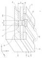
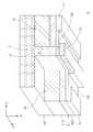
도 1은 본 발명의 일 실시형태에 따른 반도체 소자(1)를 나타낸 사시도이다.1 is a perspective view showing a
도 1을 참조하면, 일 실시형태에 따른 반도체 소자(1)는 제1 밴드갭을 갖는제1 반도체층(110)과, 상기 제1 반도체층(110) 상에 배치되며, 상기 제1 밴드갭보다 큰 제2 밴드갭을 갖는 제2 반도체층(120)과, 제3 반도체층(130)을 포함한다.
1, a
상기 제2 반도체층(120)은 상기 제1 반도체층 상면에 서로 분리되어 배치된 제1 영역(R1)과 제2 영역(R2)을 포함하며, 상기 제3 반도체층(130)은 상기 제2 반도체층(120)의 제1 영역(R1)과 제2 영역(R2) 사이에 배치된다.
The
상기 제1 반도체층(110) 하부에는 기판(101)이 배치될 수 있다. 상기 기판(101)은 반도체 성장용으로 제공되는 것으로, 도전성 또는 절연성 물질일 수 있다. 예를 들어, 상기 기판(101)은 사파이어, 실리콘(Si), 실리콘 카바이드(SiC), 질화갈륨(GaN), 질화알루미늄(AlN) 또는 산화아연(ZnO)으로 이루어질 수 있다.
The
상기 제1 반도체층(110) 및 제2 반도체층(120)은 예를 들면 III-V족 화합물 반도체로 이루어질 수 있으며, 예컨대 질화갈륨(GaN), 알루미늄 질화갈륨(AlGaN), 인듐 질화갈륨(InGaN) 및 인듐 알루미늄 질화갈륨(InAlGaN)에서 선택된 어느 하나로 형성될 수 있다. 상기 제2 반도체층(120)은 상기 제1 반도체층(110)의 밴드갭보다 큰 밴드갭을 가지며, 상기 제1 반도체층(110) 상에 적층된다. 예를 들어, 상기 제1 반도체층(110)은 GaN으로 이루어지고, 상기 제2 반도체층(120)은 AlGaN으로 이루어질 수 있다.The
이 경우, 상이한 밴드갭을 갖는 2개의 반도체층 간의 이종접합에 의해 상기 제1 및 제2 반도체층(110, 120) 간의 접합계면에 인접한 제1 반도체층(110)의 상부에는 2차원 전자가스층(2DEG: g)이 유발된다.In this case, a two-dimensional electron gas layer is formed on the upper portion of the
일 실시형태에 따르면, 상기 제1 및 제2 반도체층(110, 120)은 의도적으로 불순물이 도핑되지 않은 언도프 반도체일 수 있으나, 이에 제한되는 것은 아니며 불순물이 도핑된 반도체로 구현될 수도 있다. 예를 들면 n형 불순물이 도핑된 반도체로 구현될 수도 있다.
According to an exemplary embodiment, the first and
일 실시형태에서, 상기 제2 반도체층(120)의 제1 및 제2 영역(R1, R2) 상에는 각각 소스 전극(11)과 드레인 전극(12)이 배치될 수 있다.In an exemplary embodiment, the
상기 소스 전극(11) 및 드레인 전극(12)은 상기 제2 반도체층(120)과 오믹접촉을 이룰 수 있다. 상기 소스 전극(11) 및 드레인 전극(12)은 Cr, Al, Ta, Ti, Au, W, TiN, Ni 및 이들의 합금으로 구성되는 그룹으로부터 선택된 적어도 하나의 물질을 포함할 수 있다. 여기서, 상기 소스 전극(11)과 드레인 전극(12)은 동일한 금속 물질로 형성된 것으로 예시되었으나, 이에 제한되는 것은 아니다. 예를 들어, 상기 소스 전극(11) 및 드레인 전극(12)은 2 이상의 금속물질이 적층된 구조, 예컨대 Ti/Al/Ni/Au이 적층된 구조를 가질 수 있다.
The
상기 제3 반도체층(130)은 상기 제2 반도체층(120)의 제1 영역(R1)과 제2 영역(R2) 사이에서 상기 제1 영역(R1)과 제2 영역(R2)이 분리되도록 배치될 수 있으며, 상기 제1 반도체층(110)의 적어도 일부까지 연장될 수 있다. 이에 따라, 상기 제1 및 제2 반도체층(110, 120) 간의 이종접합에 의해 상기 제1 반도체층(110)의 상부에 유발되는 2차원 전자가스층(g)은 상기 제3 반도체층(130)을 사이에 두고 두 개의 영역으로 분리될 수 있다. 즉, 상기 반도체 소자(1)의 동작 온(On)시 전류의 흐름은 상기 2차원 전자가스층(g)을 통해 이루어지는데, 일 실시형태는 제3 반도체층(130)이 2차원 전자가스층(g)을 분리시키므로, 게이트 전압이 0V인 경우 전류의 흐름이 차단되는 노멀리-오프 동작이 가능한 반도체 소자가 구현될 수 있다.
In the
일 실시형태의 반도체 소자(1)에서, 상기 제1 및 제2 반도체층(110, 120)은 도 1에 도시된 바와 같이 제2 반도체층(120)을 관통하여 적어도 상기 제1 반도체층(110)의 일부까지 연장되는 리세스부(r1)를 포함하고, 상기 제3 반도체층(130)은 상기 리세스부(r1) 상에 배치될 수 있다. 여기서, 상기 리세스부(r1)는 x방향으로 연장되어 2차원 전자가스층(g)을 두 개의 영역으로 분리시킬 수 있다.
In the
일반적으로, 노멀리-오프 동작을 구현하고자 상기 2차원 전자가스층(g)을 분리시키는 리세스부(r1)를 형성할 경우, 반도체 소자의 동작 특성은 리세스부(r1)의 두께(ta)와 폭(d)에 의해 결정되며, 따라서 리세스부의 두께(ta)와 폭(d)의 정밀한 제어가 요구된다. 또한, 높은 문턱전압이 요구되는 환경에서 사용되는 반도체 소자는 리세스부(r1)의 두께(ta)나 폭(d)을 크게 설정할 필요가 있으나, 이 경우 소자의 온(On) 저항이 함께 증가하는 문제가 제기될 수 있다.
In general, when the recess portion r1 is formed to separate the two-dimensional electron gas layer g so as to implement a normally-off operation, an operation characteristic of the semiconductor device is the thickness ta of the recess portion r1. And width d, so precise control of the thickness ta and width d of the recess is required. In addition, in the semiconductor device used in an environment requiring a high threshold voltage, it is necessary to set the thickness ta or the width d of the recess part r1 to be large, but in this case, the on resistance of the device may be Increasing problems can be raised.
반면, 일 실시형태의 반도체 소자(1)에 따르면, 상기 2차원 전자가스층(g)은 상기 리세스부(r1) 상에 배치된 제3 반도체층(130)에 의해 분리되며, 상기 제3 반도체층(130)은 불순물을 포함하는 채널 영역(c)을 포함한다.
On the other hand, according to the
상기 채널 영역(c)은 상기 제3 반도체층에 의해 분리된 2차원 전자가스층(g)의 두 영역과 각각 접하도록 배치될 수 있으며, 게이트 전극(13)에 문턱전압 이상의 전압이 인가되면 상기 분리된 2차원 전자가스층(g)을 서로 연결하는 채널을 형성할 수 있다.
The channel region c may be disposed to contact two regions of the two-dimensional electron gas layer g separated by the third semiconductor layer, and may be separated when a voltage equal to or greater than a threshold voltage is applied to the
이에 제한되는 것은 아니지만, 상기 채널 영역(c)은 상기 제3 반도체층(130)에 불순물을 주입하여 형성될 수 있다. 예를 들면, 상기 제3 반도체층(130)에 p형 도펀트를 주입하여 채널 영역(c)을 형성할 수 있다. 이 경우, 게이트 전극(13)에 문턱전압 이상의 (+)전압이 인가되면 전계 효과에 의해 p형 도펀트가 상기 게이트 전극(13)이 배치된 방향의 반대방향으로 이동됨으로써 상기 채널 영역(c)에는 공핍영역이 형성되고, 상기 분리된 2차원 전자가스층(g)은 상기 공핍영역을 경유하여 전류가 흐르게 된다.
Although not limited thereto, the channel region c may be formed by injecting impurities into the
이 경우, 일 실시형태의 반도체 소자(1)는 상기 채널 영역(c)에 포함된 불순물의 도핑량에 따라 문턱전압이 결정될 수 있다. 구체적으로, 높은 문턱전압이 요구되는 반도체 소자를 구현하고자 할 경우, 채널 영역(c)에 포함된 p형 도펀트의 도핑량을 크게 설정하고, 반대로 낮은 문턱전압이 요구되는 반도체 소자는 p형 도펀트의 도핑량을 작게 설정함으로써 구현할 수 있다. 즉, 일 실시형태에 따르면, 상기 리세스부(r1)의 두께(ta)와 폭(d)의 정밀한 제어가 없더라도, 상기 채널 영역(c)에 포함된 불순물의 도핑량을 제어함으로써 문턱전압을 달리 설정할 수 있으며, 아울러 문턱전압이 클 경우 온(On) 저항이 함께 증가하는 이른바 트레이드-오프 관계에 종속되지 않는 노멀리-오프 동작의 반도체 소자를 구현할 수 있다. 한편, 상기 채널 영역(c)은 상기 게이트 절연층(22)과 소정 거리 이격되어 형성된 것으로 도시되었으나, 이에 제한되는 것은 아니므로, 상기 게이트 절연층(22)의 하면과 접하도록 상기 제3 반도체층(130) 내에서 상부로 연장되어 형성될 수도 있다.
In this case, in the
이에 제한되는 것은 아니지만, 상기 제3 반도체층(130)은 상기 제1 및 제2 반도체층(110, 120)과 다른 물질로 이루어질 수 있으며, 예를 들면 IV족 반도체로 이루어질 수 있다. 이때, 상기 제3 반도체층(130)은 실리콘 반도체로 이루어질 수 있다. 예를 들면 상기 제3 반도체층(130)은 비정질 실리콘, 다결정 실리콘 및 단결정 실리콘 중 적어도 하나로 이루어질 수 있다. 단결정 실리콘은 저항이 낮고, 캐리어의 이동도가 높은 특성이 있어 전류가 보다 원활하게 채널을 통과할 수 있으며, 이에 따라 반도체 소자의 온(On)저항 특성이 보다 개선될 수 있다.
Although not limited thereto, the
아울러, 상기 제3 반도체층(130)으로 III-V족 반도체(예컨대, GaN)가 아닌 IV족 반도체(예컨대, Si)를 이용하는 경우, 후술할 바와 같이 상기 제3 반도체층(130) 상에 보다 고품질의 게이트 절연층(22)을 형성할 수 있다.
In addition, in the case of using a group IV semiconductor (eg, Si) instead of a group III-V semiconductor (eg, GaN) as the
일 실시형태에서, 상기 제3 반도체층(130) 상에는 게이트 절연층(22)이 배치될 수 있다. 상기 게이트 절연층(22)은 절연물질, 예컨대 실리콘 산화물(SiOx), 실리콘 질화물(SiNx), 하프늄 질화물(HfN) 또는 Al2O3등의 금속산화물로 이루어질 수 있다.In one embodiment, the
일 실시형태에서, 상기 제3 반도체층(130) 상에 배치된 게이트 절연층(22)은 열산화막일 수 있다. 일반적으로, III-V족 반도체, 예컨대 GaN계 반도체층 상에 산화막을 형성하는 경우, GaN계 반도체층의 손상 가능성을 고려하여 약 250℃ 내지 300℃의 온도에서 산화막을 형성하므로, 고품질의 절연층을 형성하기 어려운 문제가 있다. 반면, 일 실시형태의 경우, 상기 제3 반도체층(130)으로서 IV족 반도체, 예를 들면 실리콘(Si) 반도체를 이용하는 경우, 상기 게이트 절연층(22)의 증착 시 약 900℃ 이상의 고온 공정이 가능하므로, 불순물 농도가 저감된 고품질의 열산화막으로 게이트 절연층(22)을 형성할 수 있다.
In an exemplary embodiment, the
상기 게이트 절연층(22) 상에는 게이트 전극(13)이 배치될 수 있다. 상기 게이트 전극(13)은 Cr, Al, Ta, Ti, Au, W, TiN, Ni 및 이들의 합금으로 구성되는 그룹으로부터 선택된 적어도 하나의 물질을 이용하여 형성될 수 있다.
The
또한, 상기 소스 전극(11)과 게이트 전극(13) 및 드레인 전극(12)과 게이트 전극(13) 사이에는 원하지 않은 전기적 단락을 방지하기 위해 패시베이션층(24)이 배치될 수 있다.
In addition, a
일 실시형태에 따르면, 채널 영역(c)에 포함되는 불순물의 도핑량을 제어함으로써 리세스부(r1)의 형태에 무관하게 문턱전압을 정밀하게 설정할 수 있고, 온(On) 저항 특성이 개선된 노멀리-오프 특성을 갖는 반도체 소자를 얻을 수 있다.
According to one embodiment, the threshold voltage can be precisely set regardless of the shape of the recess portion r1 by controlling the doping amount of the impurity contained in the channel region c, and the on resistance characteristic is improved. A semiconductor device having normally-off characteristics can be obtained.
도 2는 도 1의 변형된 실시형태를 설명하기 위한 사시도이다. 여기서는, 도 1의 실시형태와 동일하게 적용될 수 있는 사항은 생략하고, 달라진 구성을 설명하기로 한다.
FIG. 2 is a perspective view for explaining a modified embodiment of FIG. 1. FIG. Here, the matters that can be applied in the same manner as in the embodiment of FIG. 1 will be omitted, and the changed configuration will be described.
도 2를 참조하면, 일 실시형태에 따른 반도체 소자(2)는 기판(101)과 제1 반도체층(110) 사이에 배치된 버퍼층(103)을 더 포함할 수 있다. 상기 버퍼층(103)은 상기 기판(101)과 제1 반도체층(110) 간의 격자상수와 열팽창 계수 불일치로 인해 반도체층의 품질이 저하되는 것을 완화하기 위해 제공된다. 이에 제한되는 것은 아니지만, 상기 버퍼층(103)은 예를 들면 알루미늄 질화막(AlN)으로 이루어질 수 있다. 다만 이에 제한되는 것은 아니다. 예를 들면 GaN, ZrB2, HfB2, ZrN, HfN, TiN 등의 물질도 상기 버퍼층(103)으로 채용될 수 있으며, 상기 버퍼층(103)은 복수의 층의 조합으로 형성될 수도 있다.
Referring to FIG. 2, the
아울러, 상기 반도체 소자(2)는 상기 버퍼층(103)과 상기 제1 반도체층(110) 사이에 배치된 고저항 반도체층(105)을 더 포함할 수 있다. 상기 고저항 반도체층(105)은 누설전류를 방지하기 위해 상대적으로 높은 저항을 가질 수 있으며, 예를 들어, 상기 제1 반도체층(110)보다 높은 저항을 가질 수 있다. 예를 들면, 상기 고저항 반도체층(105)은 반절연성 GaN층일 수 있다. 또한, 상기 고저항 반도체층(105)은 Al의 조성이 점진적으로 그레이딩되는 AlGaN층으로 이루어져, 누설전류를 효과적으로 차단하는 기능을 수행할 수 있다.
In addition, the
이하에서는, 도 3a 내지 도 3f를 참조하여 상술한 도 2의 실시형태에 따른 반도체 소자(2)를 제조하는 방법을 보다 상세하게 설명하기로 한다.Hereinafter, a method of manufacturing the
일 실시형태에 따른 제조방법은, 도 3a에 도시된 바와 같이, 기판(101) 상에 제1 밴드갭을 갖는 제1 반도체층(110)과, 상기 제1 밴드갭 보다 큰 제2 밴드갭을 갖는 제2 반도체층(120)을 형성하는 단계(S10)부터 시작될 수 있다. 이 경우, 상이한 밴드갭을 갖는 2개의 반도체층 간의 이종접합에 의해 상기 제1 및 제2 반도체층(110, 120) 간의 접합계면에 인접한 제1 반도체층(110)의 상부에는 2차원 전자가스층(g)이 유발될 수 있다.
According to an exemplary embodiment of the present disclosure, as illustrated in FIG. 3A, a
일 실시형태에서, 상기 제1 반도체층(110)은 상기 기판(101) 상에 버퍼층(103) 및/또는 고저항 반도체층(105)을 형성한 이후 상기 버퍼층(103) 및/또는 고저항 반도체층(105) 상에 형성할 수도 있다.
In one embodiment, the
본 단계(S10)는 당 기술 분야에서 공지된 유기 금속 화학 증착(Metal Organic Chemical Vapor Deposition, MOCVD), 수소화 기상 에피택시(Hydride Vapor Phase Epitaxy, HVPE), 분자선 에피택시(Molecular Beam Epitaxy, MBE) 등과 같은 반도체층 성장 공정을 이용하여 수행될 수 있다.
This step (S10) is a metal organic chemical vapor deposition (MOCVD), hydrogen vapor phase epitaxy (HVPE), molecular beam epitaxy (MBE) and the like known in the art It can be performed using the same semiconductor layer growth process.
다음으로, 도 3b에 도시된 바와 같이, 상기 제2 반도체층(120)을 관통하여 적어도 상기 제1 반도체층(110)의 일부까지 연장되는 리세스부(r1)를 형성한다(S20). 이 경우, 상기 제2 반도체층(120)과, 상기 제1 반도체층(110)의 일부는 상기 리세스부(r1)에 의해 제1 영역(R1)과 제2 영역(R2)으로 분리될 수 있다. 이에 따라, 상기 제1 반도체층(110) 상부에 유발되는 2차원 전자가스층(g)이 상기 리세스부(r1)에 의해 분리되는 것으로 이해될 수 있다. 본 단계(S20)는 예를 들면, 건식 식각 또는 습식 식각과 같은 반도체층 식각공정을 이용하여 수행될 수 있다.
Next, as shown in FIG. 3B, a recess portion r1 extending through at least a portion of the
다음으로, 상기 리세스부(r1) 상에 제3 반도체층(130)을 형성한다(S30). 상기 제3 반도체층(130)은 상기 리세스부(r1)의 적어도 일부를 메우도록 형성되며, 상기 2차원 전자가스층(g)은 상기 제3 반도체층(130)에 의해 두 개의 영역으로 분리되어 이격되는 형태가 된다고 할 수 있다.Next, a
이에 제한되는 것은 아니지만, 상기 제3 반도체층(130)은 상기 제1 및 제2 반도체층(110, 120)과 다른 물질로 이루어질 수 있으며, 예컨대 IV족 반도체일 수 있다. 이 경우, 상기 제3 반도체층(130)은 비정질 실리콘, 다결정 실리콘 및 단결정 실리콘 중 적어도 하나로 이루어질 수 있다. 여기서, 단결정 실리콘은 저항이 낮고 캐리어의 이동도가 높은 특성을 가지므로, 반도체 소자의 온(On)저항 특성이 보다 개선될 수 있다.
Although not limited thereto, the
본 단계(S30)는 예를 들면, 도 3c에 도시된 바와 같이 상기 제2 반도체층(120) 및 리세스부(r1) 상에 비정질 실리콘 또는 다결정 실리콘으로 이루어지는 반도체층(130')을 증착하는 단계(S31)를 포함할 수 있다.In the step S30, for example, as illustrated in FIG. 3C, the
이후, 상기 증착된 비정질 실리콘 또는 다결정 실리콘으로 이루어지는 반도체층(130') 중 상기 제2 반도체층(120) 상에 형성된 영역을 연마 등의 공정을 이용하여 제거하고(S32), 상기 잔여하는 비정질 실리콘 또는 다결정 실리콘으로 이루어지는 반도체층(130')에 레이저 어닐링 및/또는 고온 어닐링을 적용하여 상기 반도체층(130')을 재결정화 시키며(S33), 이에 따라 도 3d에 도시된 것과 같이 단결정 실리콘으로 이루어지는 제3 반도체층(130)을 형성할 수 있다.
Subsequently, a region formed on the
다음으로, 도 3e에 도시된 바와 같이, 상기 제3 반도체층(130) 상에 게이트 절연층(22)을 형성한다(S40). 상기 게이트 절연층(22)은 실리콘 산화물(SiOx), 실리콘 질화물(SiNx), 하프늄 질화물(HfN) 또는 Al2O3등의 금속산화물로 이루어질 수 있다.
Next, as shown in FIG. 3E, a
일 실시형태에서, 상기 게이트 절연층(22)은 퍼니스(Furnace) 장비 등을 이용하여 약 900℃ 이상의 온도에서 형성되는 열산화막일 수 있다. 특히, 제3 반도체층(130)으로 실리콘(Si) 반도체를 이용하는 경우, 게이트 산화막 형성 시 GaN계 반도체층 상에 산화막을 형성하는 경우에 비해 고온 공정을 적용할 수 있으므로, 불순물이 저감된 고품질의 게이트 절연층(22)을 얻을 수 있다. 이에 제한되는 것은 아니지만, 이 경우 상기 열산화막은 SiO2로 이루어질 수 있다. 이때, 제3 반도체층(130)으로 실리콘 반도체를 채용할 경우, 상기 제3 반도체층(130)의 상면에서 일부 두께(tb)까지는 산화작용에 의해 게이트 절연층(22)으로 변형될 수 있으며, 이에 따라 상기 게이트 절연층(22)은 새롭게 증착되는 산화막 두께(tc)의 합에 의해, 전체 tb+tc의 두께로 제공될 수 있다. 추후 공정에서 상기 게이트 절연층(22) 상에 게이트 전극(13)을 배치할 경우, 상기 게이트 전극(13)은 그 하면이 소스 전극(11) 및 드레인 전극(12)의 하면보다 높은 레벨(도 3f의 tc참조)에 위치할 수 있다. 다만, 이에 한정되는 것은 아니므로, 도 5와 관련된 설명에서 후술할 바와 같이, 상기 게이트 전극(13)의 하면은 소스 전극(11) 및 드레인 전극(12)의 하면보다 낮은 레벨에 위치할 수도 있다.
In an exemplary embodiment, the
한편, 상기 게이트 절연층(22)은 플라즈마 강화 화학증기증착(Plasma enhanced chemical vapor deposition, PECVD), 저압 화학기상증착(Low pressure CVD, LPDVD), 원자층 증착(Atomic layer deposition, ALD) 등의 공정을 이용해서 형성할 수도 있다.
On the other hand, the
다음으로, 상기 제3 반도체층(130)에 불순물을 포함하는 채널 영역(c)을 형성한다(S50). 본 단계(S50)는 이온 임플란트 공정을 이용하여 상기 제3 반도체층(130)에 불순물을 주입하는 것으로 수행될 수 있다.Next, a channel region c including impurities is formed in the third semiconductor layer 130 (S50). The step S50 may be performed by implanting impurities into the
상기 채널 영역(c)은 상기 제1 반도체층(110)과 제2 반도체층(120)의 접합계면에 인접한 제1 반도체층(110)의 상부 영역, 보다 구체적으로는 상기 제1 및 제2 반도체층(110, 120)의 이종 접합에 의해 유발되는 2차원 전자가스층(g)이 형성된 영역과 대응되는 위치를 타겟으로 하여 불순물을 주입하는 것으로 형성될 수 있다.The channel region c is an upper region of the
이에 제한되는 것은 아니지만, 일 실시형태에서 상기 불순물은 p형 도펀트일 수 있으며, p형 도펀트로는 예컨대 Mg, Be, B 등을 이용할 수 있다. 일 실시형태에서, 상기 제3 반도체층(130)을 실리콘 반도체로 형성하는 경우, 상기 채널 영역(c)은 p형 불순물이 도프된 실리콘 반도체가 될 수 있다.
In some embodiments, the impurity may be a p-type dopant, and as the p-type dopant, for example, Mg, Be, B, or the like may be used. In one embodiment, when the
다음으로, 상기 게이트 절연층(22) 상에 게이트 전극(13)을 배치하고, 상기 제2 반도체층(120)의 제1 및 제2 영역(R1, R2) 상에 소스 전극(11)과 드레인 전극(12)을 각각 배치하여 도 3f에 도시된 것과 같은 반도체 소자가 얻어질 수 있다.
Next, the
일 실시형태에서, 상기 소스 전극(11)과 게이트 전극(13) 및 드레인 전극(12)과 게이트 전극(13) 사이에는 원하지 않은 전기적 단락을 방지하기 위해 패시베이션층(24)을 더 형성할 수 있다.In one embodiment, a
도시된 바와 같이, 상기 소스 전극(11), 게이트 전극(13) 및 드레인 전극(12)과 각각 접속되는 소스 패드(11p), 게이트 패드(13p) 및 드레인 패드(12p)를 더 포함할 수 있다. 상기 패드전극들 간의 원하지 않은 전기적 단락을 방지하고자 상부 패시베이션층(26)이 더 형성될 수 있다. 상기 패시베이션층(24) 및 상부 패시베이션층(26)은 예컨대 실리콘 산화물(SiOx), 실리콘 질화물(SiNx), 하프늄 질화물(HfN) 또는 Al2O3등의 금속산화물과 같은 절연물질로 이루어질 수 있다.
As shown, the
도 4a 및 도 4b는 도 2의 변형된 실시형태를 설명하기 위한 단면도이다. 여기서는, 도 2의 실시형태와 동일하게 적용될 수 있는 사항은 생략하고, 달라진 구성을 설명하기로 한다.
4A and 4B are cross-sectional views illustrating the modified embodiment of FIG. 2. Here, the matters that can be applied in the same manner as in the embodiment of FIG. 2 will be omitted, and the changed configuration will be described.
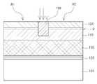
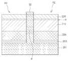
도 4a를 참조하면, 일 실시형태에 따른 반도체 소자(3)는 제2 반도체층(120)의 분리된 제1 및 제2 영역(R1, R2)사이에 배치되며, 제1 반도체층(110)을 관통하는 제3 반도체층(130)을 포함할 수 있다.Referring to FIG. 4A, the
일 실시형태는, 상기 제2 반도체층(120)과 상기 제1 반도체층(110)을 모두 관통하는 리세스부(r2)를 포함하고, 상기 리세스부(r2)를 메우도록 상기 리세스부 (r2)상에 제3 반도체층(130)이 배치된 형태로 이해될 수 있을 것이다.
An embodiment includes a recess portion r2 that penetrates both the
상기 제3 반도체층(130)에 의해 분리된 2차원 전자가스층(g)은 상기 제3 반도체층(130)에 포함된 채널 영역(c)과 접하며, 반도체 소자(3)의 문턱전압 및 온(On) 저항 특성은 상기 채널 영역(c)에 포함된 불순물의 도핑량에 따라 적절히 설정될 수 있다.
The two-dimensional electron gas layer g separated by the
일 실시형태에서, 상기 제3 반도체층(130)은 상기 제1 및 제2 반도체층(110, 120)을 관통하여 고저항 반도체층(105)의 일부까지 연장되는 것으로 도시되었으나, 이에 제한되는 것은 아니다. 구체적으로, 도 4b에 도시된 반도체 소자(4)와 같이, 상기 제3 반도체층(130)은 상기 고저항 반도체층(105) 및 버퍼층(103)을 관통하여 기판(101)까지 연장될 수 있다.In an exemplary embodiment, the
즉, 도 4b의 실시형태는, 상기 기판(101) 상에 배치된 복수의 층(예컨대, 제1 및 제2 반도체층(110, 120)과 고저항 반도체층(105) 및 버퍼층(103))을 모두 관통하여 상기 기판(101)까지 연장되는 리세스부(r3)를 포함하고, 상기 제3 반도체층(130)은 상기 리세스부(r3)를 메우도록 배치된 형태로 이해될 수 있다.
That is, in the embodiment of FIG. 4B, a plurality of layers (for example, the first and second semiconductor layers 110 and 120, the high
아울러, 도 4a 및 도 4b에 도시된 바와 같이, 상기 제3 반도체층(130) 상에는 게이트 절연층(22')이 배치될 수 있다. 상기 게이트 절연층(22')은 앞서 설명한 것과 달리, 상기 제3 반도체층(130)의 일부가 산화되어 게이트 절연층(22')으로 변형된 영역(도 3e의 tb참조)을 포함하지 않을 수 있다. 이 경우, 상기 게이트 절연층(22')은 그 하면이 상기 제2 반도체층(120)의 상면과 동일한 레벨을 갖도록 배치된 형태가 될 수 있다.
In addition, as illustrated in FIGS. 4A and 4B, a
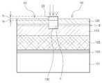
도 5는 도 2에서 변형된 실시형태를 설명하기 위한 단면도이다. 도 2의 실시형태와 동일하게 적용될 수 있는 사항은 생략하고, 달라진 구성을 설명하기로 한다.5 is a cross-sectional view for describing an embodiment modified in FIG. 2. Items that can be applied in the same manner as in the embodiment of FIG. 2 will be omitted and the changed configuration will be described.
도 5를 참조하면, 일 실시형태에 따른 반도체 소자(5)는 제2 반도체층(120)의 분리된 제1 및 제2 영역(R1, R2)사이에 배치되며, 상기 제1 반도체층(110)의 적어도 일부까지 연장되는 제3 반도체층(130)을 포함한다.
Referring to FIG. 5, the semiconductor device 5 according to the exemplary embodiment is disposed between the separated first and second regions R1 and R2 of the
일 실시형태에서, 상기 제3 반도체층(130)은 상기 제2 반도체층(120)을 관통하여 상기 제1 반도체층(110)의 일부까지 연장된 리세스부(r1) 상에 배치된다. 여기서, 도 2의 실시형태와 다르게, 상기 제3 반도체층(130)은 상기 리세스부(r1)를 완전히 메우는 형태가 아니라, 일부까지만 메우도록 배치될 수 있다.In one embodiment, the
상기 제3 반도체층(130)은 상기 제1 및 제2 반도체층(110, 120) 간의 접합계면에 인접한 제1 반도체층(110)의 상부에 유발되는 2차원 전자가스층(g)을 분리시킬 수 있도록, 상기 제1 및 제2 반도체층(110, 120)의 접합계면이 게재된 높이까지는 리세스부(r1)를 메우도록 배치될 수 있다. 일 실시형태에 따르면, 상기 제3 반도체층(130)의 상면은 상기 제2 반도체층(120)의 상면보다 낮은 레벨을 가질 수 있다.
The
상기 제3 반도체층(130) 상에는 게이트 절연층(22'')이 게재될 수 있다. 일 실시형태에서, 상기 게이트 절연층(22'')은 제3 반도체층(130) 상부에 배치되되, 상기 소스 전극(11) 및 드레인 전극(12)의 측면까지 연장되어, 소스 전극(11), 게이트 전극(13) 및 드레인 전극(12) 간의 원하지 않은 전기적 단락을 방지하는 기능도 함께 수행할 수 있다.
The
일 실시형태에서, 제3 반도체층(130)이 리세스부(r1)를 일부까지만 메우도록 배치됨에 따라, 상기 게이트 절연층(22'')은 상기 제3 반도체층(130)이 배치된 영역의 상부에서 오목한 홈을 이룰 수 있다. 이 경우, 상기 게이트 절연층(22'') 상에 형성된 게이트 전극(13)은 그 하면이 소스 전극(11) 및 드레인 전극(12) 중 적어도 하나의 하면보다 일정 두께(td)만큼 낮은 레벨에 위치할 수 있다.
In one embodiment, as the
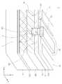
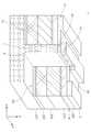
도 6은 본 발명의 일 실시형태에 따른 반도체 소자(6)를 설명하기 위한 일부 절단 사시도이다.
6 is a partially cutaway perspective view for explaining the
도 6을 참조하면, 일 실시형태에 따른 반도체 소자(6)는 반도체 기판(201)과, 상기 반도체 기판(201) 상에 배치되되, 서로 다른 밴드갭을 가지고 적층되는 제1 및 제2 반도체층(210, 220)을 포함한다. 일 실시형태에서, 상기 반도체 기판(201)은 돌출부(p)를 구비하며, 상기 제1 및 제2 반도체층(210, 220)은 상기 돌출부(p)에 의해 제1 영역(R1)과 제2 영역(R2)으로 분리된다.Referring to FIG. 6, a
상기 제1 및 제2 영역(R1, R2)에 배치된 제2 반도체층(220) 상에는 각각 소스 전극(11)과 드레인 전극(12)이 배치된다. 상기 돌출부(p) 상에는 게이트 절연층(32)이 배치될 수 있으며, 상기 게이트 절연층(32) 상에는 게이트 전극(13)이 배치될 수 있다.The
도 6에서는, 상기 돌출부(p)의 형상에 대한 이해를 돕기 위하여, 상기 돌출부(p)의 우측에 배치되는 제1 및 제2 반도체층(210, 220), 드레인 전극(12), 페시베이션층(34) 및 게이트 전극(13)의 일부가 생략되어 도시되었다.
In FIG. 6, to aid in understanding the shape of the protrusion p, the first and second semiconductor layers 210 and 220, the
상기 제1 반도체층(210)과 제2 반도체층(220)은 서로 다른 밴드갭을 가질 수 있다. 예를 들면 상기 제1 반도체층(210)은 제1 밴드갭을 가지며, 상기 제2 반도체층(220)은 상기 제1 반도체층(210)의 밴드갭(제1 밴드갭) 보다 큰 제2 밴드갭을 가질 수 있다. 이에 따라, 상기 제1 및 제2 반도체층(210, 220) 간의 접합계면에 인접한 제1 반도체층(210)의 상부에는 2차원 전자가스층(g)이 유발될 수 있다.
The
상기 돌출부(p)는 상기 제1 및 제2 반도체층(210, 220)을 각각 제1 영역(R1)과 제2 영역(R2)으로 분리시킨다. 이에 따라, 상기 2차원 전자가스층(g)은 돌출부(p)를 사이에 두고 분리되며, 상기 반도체 소자(6)는 게이트 전압이 0V인 경우 전류의 흐름이 차단되는 노멀리-오프 동작이 가능하게 된다.The protrusion p separates the first and second semiconductor layers 210 and 220 into a first region R1 and a second region R2, respectively. Accordingly, the two-dimensional electron gas layer g is separated with the protrusion p interposed therebetween, and the
한편, 상기 돌출부(p)는 상기 제1 반도체층(210)을 관통하여 상기 제2 반도체층(220)의 상면까지 연장되는 것으로 도시되었으나, 이에 제한되는 것은 아니다. 따라서, 도 9에서 후술할 바와 같이, 상기 돌출부(p)는 제1 반도체층(210)을 관통하되, 그 상면은 상기 제2 반도체층(220)의 상면보다 낮은 레벨에 위치할 수도 있다.
On the other hand, the protrusion p is shown to extend through the
상기 돌출부(p)는 불순물을 포함하는 채널 영역(c)을 포함한다. 일 실시형태에서, 상기 채널 영역(c)은 상기 돌출부에 의해 분리된 2차원 전자가스층(g)의 두 영역과 각각 접하도록 배치될 수 있으며, 게이트 전극(13)에 문턱전압 이상의 전압이 인가되면 분리된 2차원 전자가스층(g)을 서로 연결하는 채널을 형성할 수 있다. 이에 제한되는 것은 아니지만, 상기 채널 영역(c)은 상기 돌출부(p)에 불순물을 주입하여 형성될 수 있다. 예를 들면, 상기 채널 영역(c)은 상기 돌출부(p)에 p형 도펀트를 주입하여 형성될 수 있다.The protrusion p includes a channel region c containing impurities. In one embodiment, the channel region (c) may be arranged to contact the two regions of the two-dimensional electron gas layer (g) separated by the protrusion, and when a voltage equal to or higher than a threshold voltage is applied to the
즉, 일 실시형태는, 도 1의 실시형태에서 제1 반도체층(210) 하부에 반도체 기판(201)이 배치되고, 제3 반도체층이 상기 반도체 기판(201)에서 돌출되어 상기 제1 반도체층(210)을 관통하는 돌출부(p)로 게재된 형태로도 이해될 수 있다.
That is, in one embodiment, in the embodiment of FIG. 1, the
한편, 상기 채널 영역(c)은 상기 게이트 절연층(32)과 소정 거리 이격되어 배치된 것으로 도시되었으나, 이에 제한되는 것은 아니므로, 상기 게이트 절연층(32)의 하면과 접하도록 형성될 수도 있다.
On the other hand, the channel region (c) is shown as being disposed spaced apart from the
일 실시형태에서, 상기 반도체 기판(201)은 상기 돌출부(p)에 불순물 도핑이 가능한 반도체 물질이라면 특별히 한정되지 않으며, 제1 및 제2 반도체층(210, 220)을 이루는 물질과 동일한 물질이거나, 다른 물질로 이루어질 수 있다. 예를 들면, 상기 반도체 기판(201)은 실리콘(Si), 실리콘 카바이드(SiC), 또는 질화갈륨(GaN)으로 이루어질 수 있다. 실리콘으로 이루어지는 경우, 상기 반도체 기판(201) 상에 반도체층(예컨대, 제1 및 제2 반도체층(210, 220)) 성장이 용이하도록 단결정 실리콘으로 이루어질 수 있다. 다만, 이에 제한되는 것은 아니므로, 상기 반도체 기판(201)은 예를 들어 상기 반도체 기판(201)은 비정질 실리콘이나 다결정 실리콘으로 이루어질 수도 있다.
In one embodiment, the
일 실시형태에서, 상기 돌출부(p) 상에는 게이트 절연층(32)이 배치된다. 상기 게이트 절연층(32)은 예를 들면 실리콘 산화물(SiOx), 실리콘 질화물(SiNx), 하프늄 질화물(HfN) 또는 Al2O3등의 금속산화물과 같은 절연 물질로 이루어질 수 있다. 일 실시형태에서, 상기 반도체 기판(201)으로 실리콘(Si) 반도체를 이용하는 경우, 불순물 농도가 저감된 고품질의 열산화막으로 게이트 절연층(32)을 형성할 수도 있다.
In one embodiment, a
상기 게이트 절연층(32) 상에는 게이트 전극(13)이 배치될 수 있다. 상기 게이트 전극(13)은 Cr, Al, Ta, Ti, Au, W, TiN, Ni 및 이들의 합금으로 구성되는 그룹으로부터 선택된 적어도 하나의 물질을 이용하여 형성될 수 있다.
The
제1 및 제2 영역(R1, R2)으로 분리된 상기 제2 반도체층(220) 상에는 각각 소스 전극(11) 및 드레인 전극(12)이 배치될 수 있다. 상기 소스 전극(11) 및 드레인 전극(12)은 Cr, Al, Ta, Ti, Au, W, TiN, Ni 및 이들의 합금으로 구성되는 그룹으로부터 선택된 적어도 하나의 물질을 포함할 수 있다. 여기서, 상기 소스 전극(11)과 드레인 전극(12)은 동일한 금속 물질로 형성될 수 있으나, 이에 제한되는 것은 아니다. 예를 들어, 2 이상의 금속물질이 적층된 구조, 예컨대 Ti/Al/Ni/Au이 적층된 구조를 가질 수 있다.
A
상기 소스 전극(11)과 게이트 전극(13) 및 드레인 전극(12)과 게이트 전극(13) 사이에는 원하지 않은 전기적 단락을 방지하기 위해 패시베이션층(34)이 배치될 수 있다.
A
일 실시형태에 따르면, 노멀리-오프 동작이 가능한 반도체 소자(6)를 구현함에 있어서 리세스부를 형성할 필요가 없는바 리세스부의 정밀한 두께나 폭의 제어가 요구되지 않으며, 채널 영역(c)의 불순물 도핑량을 제어하는 것을 통해 문턱전압을 용이하게 설정할 수 있는 반도체 소자를 얻을 수 있다. 아울러, 상기 제1 및 제2 반도체층(210, 220)은 돌출부(p)에 의해 제1 및 제2 영역(R1, R2)으로 분리된 반도체 기판(201) 상에서 성장되므로, 성장 시 발생하는 스트레인 등의 저감 효과로 인해 우수한 결정품질을 가질 수 있는 이점이 있다.
According to one embodiment, in the implementation of the
도 7은 도 6의 변형된 실시형태를 설명하기 위한 일부 절단 사시도이다. 여기서는, 도 6의 실시형태와 동일하게 적용될 수 있는 사항은 생략하고, 달라진 구성을 설명하기로 한다.
FIG. 7 is a partially cutaway perspective view for explaining a modified embodiment of FIG. 6. FIG. Here, the matters that can be applied in the same manner as in the embodiment of FIG. 6 will be omitted, and the changed configuration will be described.
도 7을 참조하면, 일 실시형태에 따른 반도체 소자(7)는 반도체 기판(201)과 상기 제1 반도체층(210) 사이에 배치된 버퍼층(203)을 더 포함할 수 있다. 또한, 상기 버퍼층(203)과 제1 반도체층(210) 사이에 배치된 고저항 반도체층(205)을 더 포함할 수 있다. 이 경우, 상기 버퍼층(203) 및 고저항 반도체층(205)은 상기 돌출부(p)에 의해 제1 영역(R1)과 제2 영역(R2)으로 분리될 수 있다.Referring to FIG. 7, the
도 7에서는, 상기 돌출부(p)의 형상에 대한 이해를 돕기 위하여, 상기 돌출부(p)의 우측에 배치되는 버퍼층(203), 고저항 반도체층(205), 제1 및 제2 반도체층(210, 220), 드레인 전극(12), 페시베이션층(34) 및 게이트 전극(13)의 일부가 생략되어 도시되었다.
In FIG. 7, the
상기 버퍼층(203)은 상기 기판과 제1 반도체층(210) 간의 격자상수와 열팽창 계수 불일치로 인해 반도체층의 품질이 저하되는 것을 완화하기 위해 제공된다. 상기 버퍼층(203)은 알루미늄 질화막(AlN)으로 이루어질 수 있으나, 이에 제한되는 것은 아니다. 예를 들면 GaN, ZrB2, HfB2, ZrN, HfN, TiN 등의 물질도 상기 버퍼층(103)으로 채용될 수 있으며, 상기 버퍼층(103)은 복수의 층의 조합으로 형성될 수도 있다.
The
상기 고저항 반도체층(205)은 누설전류를 방지하기 위해 비교적 높은 저항을 가질 수 있다. 상기 고저항 반도체층(205)은 반절연성 GaN층일 수 있다. 또한, Al의 조성이 점진적으로 그레이딩되는 AlGaN층으로 이루어질 수도 있다.
The high
이하에서는, 도 8a 내지 도 8e를 참조하여 상술한 도 7의 실시형태에 따른 반도체 소자(7)를 제조하는 방법을 보다 상세하게 설명하기로 한다.
Hereinafter, a method of manufacturing the
일 실시형태에 따른 제조방법은, 도 8a에 도시된 바와 같이, 반도체 기판(201)을 마련하는 단계(S100)부터 시작될 수 있다. 일 실시형태에서, 상기 반도체 기판(201) 상에 게이트 절연층(32)을 미리 형성할 수 있다.The manufacturing method according to the exemplary embodiment may be started from the step S100 of preparing the
이에 제한되는 것은 아니지만, 상기 반도체 기판(201)으로 실리콘(Si) 반도체 를 이용하는 경우, 게이트 산화막 형성 시 GaN계 반도체층 상에 산화막을 형성하는 경우에 비해 고온 공정을 적용할 수 있으므로, 불순물이 저감된 고품질의 게이트 절연층(32)을 얻을 수 있다. 여기서, 상기 게이트 절연층(32)은 퍼니스 장비 등을 이용하여 약 900℃ 이상의 온도에서 형성되는 열산화막일 수 있다.Although not limited thereto, since a silicon (Si) semiconductor is used as the
다만, 이에 제한되는 것은 아니므로 상기 게이트 절연층(32)은 플라즈마 강화 화학증기증착(Plasma enhanced chemical vapor deposition, PECVD), 저압 화학기상증착(Low pressure CVD, LPDVD), 원자층 증착(Atomic layer deposition, ALD) 등의 공정을 이용해서 형성할 수도 있다.
However, the present invention is not limited thereto, and the
다음으로, 도 8b에 도시된 바와 같이, 상기 반도체 기판(201)에 돌출부(p)를 형성한다(S200). 상기 돌출부(p)는 상기 반도체 기판(201)에서 돌출부(p)가 형성될 영역을 제외한 나머지 영역을 제거하는 것으로 수행될 수 있다. 본 단계(S200)는, 예를 들면 식각공정 등을 이용할 수 있다.
Next, as shown in FIG. 8B, a protrusion p is formed on the semiconductor substrate 201 (S200). The protrusion p may be performed by removing a portion of the
다음으로, 도 8c에 도시된 바와 같이, 상기 반도체 기판(201) 상에 서로 다른 밴드갭을 갖는 제1 및 제2 반도체층(210, 220)을 형성한다(S300). 상기 제1 및 제2 반도체층(210, 220) 각각은 상기 돌출부(p)에 의해 제1 및 제2 영역(R1, R2)으로 분리되어 형성될 수 있다.Next, as shown in FIG. 8C, first and second semiconductor layers 210 and 220 having different band gaps are formed on the semiconductor substrate 201 (S300). Each of the first and second semiconductor layers 210 and 220 may be separated into the first and second regions R1 and R2 by the protrusion p.
본 단계(S300)에서, 상이한 밴드갭을 갖는 2개의 반도체층 간의 이종접합에 의해 상기 제1 및 제2 반도체층(210, 220) 간의 접합계면에 인접한 제1 반도체층(210)의 상부에는 2차원 전자가스층(g)이 유발될 수 있다.
In this step (S300), two heterojunctions between the two semiconductor layers having different band gaps result in two on top of the
일 실시형태에서, 상기 제1 반도체층(210)은 상기 반도체 기판(201) 상에 버퍼층(203) 및/또는 고저항 반도체층(205)을 형성한 이후 상기 버퍼층(203) 및/또는 고저항 반도체층(205) 상에 형성할 수도 있다.
In one embodiment, the
본 단계(S300)는 당 기술 분야에서 공지된 유기 금속 화학 증착(Metal Organic Chemical Vapor Deposition, MOCVD), 수소화 기상 에피택시(Hydride Vapor Phase Epitaxy, HVPE), 분자선 에피택시(Molecular Beam Epitaxy, MBE) 등과 같은 반도체층 성장 공정을 이용하여 수행될 수 있다.
This step (S300) is a metal organic chemical vapor deposition (MOCVD), hydrogen vapor phase epitaxy (HVPE), molecular beam epitaxy (MBE) and the like known in the art It can be performed using the same semiconductor layer growth process.
다음으로, 도 8d에 도시된 바와 같이, 상기 돌출부(p)에 불순물을 포함하는 채널 영역(c)을 형성한다(S400). 본 단계(S400)는 이온 임플란트 공정을 이용하여 상기 돌출부(p)에 불순물을 주입하는 것으로 수행될 수 있다.
Next, as shown in FIG. 8D, a channel region c including impurities is formed in the protrusion p (S400). The step S400 may be performed by injecting impurities into the protrusion p using an ion implant process.
상기 채널 영역(c)은 상기 제1 반도체층(210)과 제2 반도체층(220)의 접합계면에 인접한 제1 반도체층(210)의 상부 영역, 보다 구체적으로는 상기 제1 및 제2 반도체층(210, 220)의 이종 접합에 의해 유발되는 2차원 전자가스층(g)이 형성된 영역과 대응되는 위치를 타겟으로 하여, 상기 돌출부(p)에 불순물을 주입하는 것으로 형성될 수 있다.The channel region c is an upper region of the
일 실시형태에서, 상기 불순물은 p형 도펀트일 수 있으며, p형 도펀트로는 예컨대 Mg, Be, B 등을 이용할 수 있다.
In one embodiment, the impurity may be a p-type dopant, and for example, Mg, Be, B, or the like may be used as the p-type dopant.
다음으로, 상기 게이트 절연층(32) 상에 게이트 전극(13)을 배치하고, 상기 제1 및 제2 영역(R1, R2)으로 분리된 제2 반도체층(220) 상에 각각 소스 전극(11)과 드레인 전극(12)을 배치하여, 도 8e에 도시된 것과 같은 반도체 소자가 얻어질 수 있다.
Next, the
일 실시형태에서, 상기 소스 전극(11)과 게이트 전극(13) 및 드레인 전극(12)과 게이트 전극(13) 사이에는 원하지 않은 전기적 단락을 방지하기 위해 패시베이션층(34)을 더 형성할 수 있다.
In one embodiment, a
또한, 일 실시형태에서, 상기 소스 전극(11), 게이트 전극(13) 및 드레인 전극(12)과 각각 접속되는 소스 패드(11p), 게이트 패드(13p) 및 드레인 패드(12p)를 더 형성할 수 있다. 상기 패드전극들 간의 원하지 않은 전기적 단락을 방지하기 위해, 상부 패시베이션층(36)이 더 형성될 수 있다.
Further, in one embodiment, the
상기 패시베이션층(34) 및 상부 패시베이션층(36)은 예컨대 실리콘 산화물(SiOx), 실리콘 질화물(SiNx), 하프늄 질화물(HfN) 또는 Al2O3등의 금속산화물과 같은 절연물질로 이루어질 수 있다. 상기 패시베이션층(34)과 상부 패시베이션층(36)은 서로 다른 물질일 수 있으나, 이에 제한되는 것은 아니므로 동일한 물질로 이루어질 수 있다.
The
일 실시형태에 따르면, 상기 게이트 전극(13)은 상기 소스 전극(11) 및 드레인 전극(12)보다 높은 레벨에 위치할 수 있다. 예를 들면, 도 8e에 도시된 바와 같이, 상기 게이트 전극(13)의 하면은 상기 게이트 절연층(32)의 두께(te)만큼 상기 소스 전극(11) 및 드레인 전극(12)의 하면보다 높은 레벨에 위치할 수 있다. 다만, 이에 제한되는 것은 아니므로, 도 9에서 후술할 바와 같이, 상기 게이트 전극(13)의 하면은 상기 소스 전극(11) 및 드레인 전극(12)의 하면 보다 낮은 레벨에 위치할 수 있다.
According to one embodiment, the
도 9는 도 7에서 변형된 실시형태를 설명하기 위한 단면도이다. 도 7의 실시형태와 동일하게 적용될 수 있는 사항은 생략하고, 달라진 구성을 설명하기로 한다.FIG. 9 is a cross-sectional view for describing an embodiment modified in FIG. 7. Items that can be applied in the same manner as in the embodiment of FIG. 7 will be omitted and the changed configuration will be described.
도 9를 참조하면, 일 실시형태에 따른 반도체 소자(8)는 돌출부(p)를 구비하며, 제1 및 제2 반도체층(210, 220)은 상기 돌출부(p)에 의해 각각 제1 영역(R1)과 제2 영역(R2)으로 분리된다. 여기서, 도 7의 실시형태와 다르게, 상기 돌출부(p)는 그 상면이 상기 제2 반도체층(220)의 상면보다 낮은 레벨에 위치한다. 이 경우, 상기 돌출부(p)는 상기 제1 및 제2 반도체층(210, 220) 간의 접합계면에 인접한 제1 반도체층(210)의 상부에 유발되는 2차원 전자가스층(g)을 분리시킬 수 있도록, 적어도 상기 제1 반도체층(210)의 상면까지는 연장된다.
Referring to FIG. 9, the
또한, 상기 돌출부(p) 상에는 게이트 절연층(32'')이 게재될 수 있다. 상기 게이트 절연층(32'')은 소스 전극(11), 게이트 전극(13) 및 드레인 전극(12) 간의 원하지 않은 전기적 단락을 방지하는 기능도 함께 수행할 수 있다.
In addition, a
일 실시형태에서, 상기 돌출부(p)는 제2 반도체층(220)의 상면보다 낮은 레벨에 위치함에 따라, 상기 게이트 절연층(32'')은 상기 돌출부(p)가 배치된 영역의 상부에서 오목한 홈을 이룰 수 있다. 이 경우, 상기 게이트 절연층(32'') 상에 형성된 게이트 전극(13)은 그 하면이 소스 전극(11) 및 드레인 전극(12)의 하면 중 적어도 하나의 하면보다 일정 두께(tf)만큼 낮은 레벨에 위치할 수 있다.
In one embodiment, the protrusion p is located at a lower level than the top surface of the
도 10은 본 발명의 일 실시형태에 따른 반도체 소자(9)의 상면도이다.10 is a top view of the
도 10의 실시형태는 예를 들면, 전술한 도 6의 실시형태에 적용될 수 있는 전극 구조를 설명하기 위한 상면도로 이해될 수 있다.
The embodiment of FIG. 10 may be understood, for example, from a top view for explaining the electrode structure applicable to the embodiment of FIG. 6 described above.
도 10을 참조하면, 일 실시형태에 따른 반도체 소자(9)의 소스 전극(11'), 게이트 전극(13') 및 드레인 전극(12')은 각각 가로 방향으로 연장되는 부분과 세로 방향으로 연장되는 부분을 포함할 수 있다.Referring to FIG. 10, the
구체적으로, 도 6의 실시형태를 기준으로 설명하면, 상기 돌출부(p)는 상기 반도체 소자의 반도체 기판(201) 상면을 기준으로, 상기 반도체 기판(201)의 상면에 수직한 제1 방향(예컨대, 세로 방향)으로 연장되는 부분과 상기 제1 방향에 수직한 제2 방향(예컨대, 가로 방향)으로 연장되는 부분을 포함하고, 상기 돌출부(p) 상에 게이트 절연층(32) 및 게이트 전극(13')이 적층된 구조로 이해될 수 있다.Specifically, referring to the embodiment of FIG. 6, the protrusion p is a first direction (eg, perpendicular to the top surface of the
이 경우, 제1 및 제2 영역(R1, R2)으로 분리된 2차원 전자가스층(g)을 연결하는 채널 영역(c)이 길게 형성될 수 있으므로, 소자의 온(On) 저항 특성이 보다 개선될 수 있다.
In this case, since the channel region c connecting the two-dimensional electron gas layer g separated into the first and second regions R1 and R2 may be formed long, the on resistance characteristic of the device is further improved. Can be.
이하, 도 11 및 도 12에서는 일 실시형태에 따른 반도체 소자(1 내지 9)를 이용한 장치를 예시적으로 설명하기로 한다.
Hereinafter, an apparatus using the
우선, 도 11에 도시된 바와 같이, 일 실시형태에 따른 반도체 소자(1 내지 9)는 전기자동차(1000)에 구비될 수 있다.First, as shown in FIG. 11, the
도 11을 참조하면, 일 실시형태에 따른 전기자동차(1000)는 배터리(1100) 및 모터(1400)를 포함한다. 일반적으로 차량의 구동을 위해서는 고전력이 필요하며, 배터리(1100) 출력을 승압하기 위한 수단이 요구된다. 이에, 전기자동차(1000)는 인버터(1200)를 구비할 수 있다. 상기 인버터(1200)는 상기 배터리(1100)로부터 인가된 전원을 3상의 교류 전력으로 변환하여 모터(1400)를 구동하기 위한 전원으로 변환할 수 있다.Referring to FIG. 11, an
일 실시형태에서, 상기 모터(1400)는 발전기로서 동작하는 기능을 겸할 수 있으며, 이에 따라 상기 모터(1400)에서 회생된 전력은 상기 인버터(1200)에서 다시 직류 전원으로 변환되고, 배터리(1100)에 충전될 수 있다.
In one embodiment, the
일 실시형태에서, 상기 인버터(1200)는 스위칭 소자 및 다이오드를 포함하는 구동회로를 포함할 수 있다. 여기서, 상기 스위칭 소자는 고전력, 고온 환경에 적용가능한 파워 반도체 소자로서, 앞선 실시형태에서 설명한 반도체 소자일 수 있다. 또한, 상기 전기자동차(1000)는 인버터(1200)에 구비된 구동회로를 제어하기 위한 수단으로, 제어부(1300)를 더 포함할 수 있다. 이에 제한되는 것은 아니지만, 상기 제어부(1300)는 상기 구동회로에 구비된 스위칭 소자의 온/오프 등의 동작을 제어하는 신호를 제공하는 기능을 수행할 수 있다.
In one embodiment, the
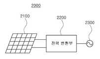
한편, 일 실시형태에 따른 반도체 소자(1 내지 9)는 도 12에 도시된 바와 같이, 태양광 발전시스템(2000)에 구비될 수 있다.Meanwhile, the
도 12를 참조하면, 일 실시형태에 따른 태양광 발전시스템(2000)은 태양광을 전기신호로 변환하여 PV(PhotoVoltaic) 신호를 출력하는 태양광 어레이(2100)와, PV 신호를 변환하여 계통(2300)으로 출력하는 전력 변환부(2200)를 포함한다. 상기 태양광 어레이(2100)는 적어도 하나 이상의 태양전지 셀을 포함할 수 있다.
Referring to FIG. 12, the photovoltaic
상기 계통(2300)을 통해 출력되는 출력 전압/전류는 일반적으로 가정, 공장 등에 공급되는 가정용/산업용 상용 전원일 수 있다.The output voltage / current output through the
태양광 어레이(2100)가 생성하는 PV 신호는 전력 변환부(2200)를 통해 계통(2300)에 전달되는 출력 전압/전류로 변환된다. 따라서, 전력 변환부(2200)는 적어도 하나의 컨버터 회로와, 상기 컨버터 회로의 동작을 제어하는 제어회로를 포함할 수 있다. 일 실시예로서, 상기 제어회로는 펄스-폭-변조 신호(PWM)를 출력하여 전력 변환부(2200)의 동작을 제어할 수 있다. 전력 변환부(2200)의 동작을 효율적으로 제어하기 위해, 상기 제어회로는 전력 변환부(2200)에 입력 및 출력으로 각각 제공되는 PV 신호 및 계통 전압을 센싱할 수 있다. 한편, 상기 컨버터 회로와, 제어회로에는 스위칭 소자가 포함될 수 있다. 여기서, 상기 스위칭 소자는 고전력 환경에 적용 가능한 파워 반도체 소자로서, 앞선 실시형태에서 설명한 반도체 소자가 채용될 수 있다.
The PV signal generated by the
본 발명은 상술한 실시형태 및 첨부된 도면에 의해 한정되는 것이 아니며 첨부된 청구범위에 의해 한정하고자 한다. 따라서, 청구범위에 기재된 본 발명의 기술적 사상을 벗어나지 않는 범위 내에서 당 기술분야의 통상의 지식을 가진 자에 의해 다양한 형태의 치환, 변형 및 변경이 가능할 것이며, 이 또한 본 발명의 범위에 속한다.
It is intended that the invention not be limited by the foregoing embodiments and the accompanying drawings, but rather by the claims appended hereto. Accordingly, various forms of substitution, modification, and alteration may be made by those skilled in the art without departing from the technical spirit of the present invention described in the claims, which are also within the scope of the present invention.
101: 기판201: 반도체 기판
103, 203: 버퍼층 105, 205: 고저항 반도체층
110, 210: 제1 반도체층120, 220: 제2 반도체층
130: 제3 반도체층p: 돌출부
11: 소스 전극12: 드레인 전극
13: 게이트 전극22, 32: 게이트 절연층
24, 34: 패시베이션층g: 2차원 전자가스층
c: 채널 영역R1: 제1 영역
R2: 제2 영역101: substrate 201: semiconductor substrate
103, 203:
110 and 210:
130: third semiconductor layer p: protrusion
11: source electrode 12: drain electrode
13:
24, 34: passivation layer g: two-dimensional electron gas layer
c: channel region R1: first region
R2: second region
Claims (10)
Translated fromKorean상기 제1 반도체층 상면에 서로 분리되어 배치된 제1 영역과 제2 영역을 포함하며, 상기 제1 밴드갭보다 큰 제2 밴드갭을 갖는 제2 반도체층; 및
상기 제2 반도체층의 상기 제1 영역과 상기 제2 영역 사이에 배치되며, 상기 제1 반도체층의 적어도 일부까지 연장되고, 상기 제1 및 제2 반도체층의 물질과 다른 반도체 물질로 이루어진 제3 반도체층;을 포함하며,
상기 제3 반도체층은 불순물이 도프된 채널 영역을 구비하고,
상기 제1 및 제2 반도체층은 Ⅲ-V족 화합물 반도체로 이루어지며,
상기 제3 반도체층은 Ⅳ족 반도체로 이루어진 것을 특징으로 하는 반도체 소자.
A first semiconductor layer having a first band gap;
A second semiconductor layer including a first region and a second region separated from each other on an upper surface of the first semiconductor layer and having a second band gap larger than the first band gap; And
A third interposed between the first region and the second region of the second semiconductor layer, extending to at least a portion of the first semiconductor layer and made of a semiconductor material different from that of the first and second semiconductor layers A semiconductor layer;
The third semiconductor layer has a channel region doped with impurities,
The first and second semiconductor layer is made of a III-V group compound semiconductor,
The third semiconductor layer is a semiconductor device, characterized in that consisting of a group IV semiconductor.
상기 제1 및 제2 반도체층 간의 접합계면과 인접한 제1 반도체층의 상부 영역에는 상기 제3 반도체층에 의해 두 개의 영역으로 분리되는 2차원 전자가스층이 위치하며,
상기 채널 영역은 상기 분리된 2차원 전자가스층의 두 개의 영역과 각각 접하도록 배치된 것을 특징으로 하는 반도체 소자.
According to claim 1,
In the upper region of the first semiconductor layer adjacent to the junction interface between the first and second semiconductor layers is a two-dimensional electron gas layer separated into two regions by the third semiconductor layer,
And the channel region is in contact with two regions of the separated two-dimensional electron gas layer, respectively.
상기 제1 및 제2 반도체층은, 상기 제2 반도체층을 관통하여 적어도 상기 제1 반도체층의 일부까지 연장되는 리세스부를 가지고,
상기 제3 반도체층은 상기 리세스부 상에 배치된 것을 특징으로 하는 반도체 소자.
According to claim 1,
The first and second semiconductor layers have recess portions extending through the second semiconductor layer to at least a portion of the first semiconductor layer,
And the third semiconductor layer is disposed on the recess portion.
상기 제1 반도체층 하부에 배치된 반도체 기판을 더 포함하고,
상기 제3 반도체층은 상기 반도체 기판에서 돌출되어 상기 제1 반도체층을 관통하는 돌출부인 것을 특징으로 하는 반도체 소자.
According to claim 1,
Further comprising a semiconductor substrate disposed below the first semiconductor layer,
And the third semiconductor layer is a protrusion protruding from the semiconductor substrate and penetrating the first semiconductor layer.
상기 돌출부는 상기 반도체 기판의 상면에 수직한 제1 방향 및 상기 제1 방향에 수직한 제2 방향으로 연장되는 것을 특징으로 하는 반도체 소자.
The method of claim 5,
And the protrusion extends in a first direction perpendicular to an upper surface of the semiconductor substrate and in a second direction perpendicular to the first direction.
상기 제2 반도체층의 제1 및 제2 영역 상에 각각 배치된 소스 전극과 드레인 전극; 및
상기 소스 전극과 드레인 전극 사이에 배치된 게이트 전극;을 더 포함하고,
상기 게이트 전극의 하면은 상기 소스 전극 및 드레인 전극의 하면 보다 높은 레벨에 배치된 것을 특징으로 하는 반도체 소자.
According to claim 1,
Source and drain electrodes respectively disposed on the first and second regions of the second semiconductor layer; And
And a gate electrode disposed between the source electrode and the drain electrode.
And a lower surface of the gate electrode is disposed at a level higher than a lower surface of the source electrode and the drain electrode.
상기 반도체 기판 상에 서로 다른 밴드갭을 가지고 적층되며, 상기 돌출부에 의해 제1 영역과 제2 영역으로 분리되는 제1 반도체층 및 제2 반도체층;을 포함하고,
상기 돌출부는 상기 제1 및 제2 반도체층과 접촉하고,
상기 돌출부는 불순물이 도프된 채널 영역을 구비하는 것을 특징으로 하는 반도체 소자.
A semiconductor substrate provided with a protrusion;
A first semiconductor layer and a second semiconductor layer stacked on the semiconductor substrate with different band gaps and separated into a first region and a second region by the protrusions;
The protrusions contact the first and second semiconductor layers,
The protrusion has a channel region doped with an impurity.
상기 제1 및 제2 반도체층 간의 접합계면과 인접한 제1 반도체층의 상부 영역에는 상기 돌출부에 의해 제1 영역과 제2 영역으로 분리되는 2차원 전자가스층이 위치하며,
상기 채널 영역은 상기 분리된 2차원 전자가스층의 제1 및 제2 영역과 각각 접하도록 배치된 것을 특징으로 하는 반도체 소자.
The method of claim 8,
In the upper region of the first semiconductor layer adjacent to the junction interface between the first and the second semiconductor layer is a two-dimensional electron gas layer is separated into the first region and the second region by the protrusion,
And the channel region is in contact with each of the first and second regions of the separated two-dimensional electron gas layer.
상기 돌출부는 상기 제1 반도체층을 관통하여 적어도 상기 제2 반도체층의 상면까지 연장되는 것을 특징으로 하는 반도체 소자.The method of claim 8,
And the protrusion extends through the first semiconductor layer to at least an upper surface of the second semiconductor layer.
Priority Applications (2)
| Application Number | Priority Date | Filing Date | Title |
|---|---|---|---|
| KR1020130152569AKR102021887B1 (en) | 2013-12-09 | 2013-12-09 | Semiconductor device |
| US14/458,288US9391186B2 (en) | 2013-12-09 | 2014-08-13 | Semiconductor device |
Applications Claiming Priority (1)
| Application Number | Priority Date | Filing Date | Title |
|---|---|---|---|
| KR1020130152569AKR102021887B1 (en) | 2013-12-09 | 2013-12-09 | Semiconductor device |
Publications (2)
| Publication Number | Publication Date |
|---|---|
| KR20150066923A KR20150066923A (en) | 2015-06-17 |
| KR102021887B1true KR102021887B1 (en) | 2019-09-17 |
Family
ID=53272022
Family Applications (1)
| Application Number | Title | Priority Date | Filing Date |
|---|---|---|---|
| KR1020130152569AActiveKR102021887B1 (en) | 2013-12-09 | 2013-12-09 | Semiconductor device |
Country Status (2)
| Country | Link |
|---|---|
| US (1) | US9391186B2 (en) |
| KR (1) | KR102021887B1 (en) |
Families Citing this family (10)
| Publication number | Priority date | Publication date | Assignee | Title |
|---|---|---|---|---|
| US9140110B2 (en) | 2012-10-05 | 2015-09-22 | Evolution Well Services, Llc | Mobile, modular, electrically powered system for use in fracturing underground formations using liquid petroleum gas |
| US11708752B2 (en) | 2011-04-07 | 2023-07-25 | Typhon Technology Solutions (U.S.), Llc | Multiple generator mobile electric powered fracturing system |
| US11255173B2 (en) | 2011-04-07 | 2022-02-22 | Typhon Technology Solutions, Llc | Mobile, modular, electrically powered system for use in fracturing underground formations using liquid petroleum gas |
| US9806182B2 (en)* | 2015-09-08 | 2017-10-31 | Macom Technology Solutions Holdings, Inc. | Parasitic channel mitigation using elemental diboride diffusion barrier regions |
| ITUB20155862A1 (en)* | 2015-11-24 | 2017-05-24 | St Microelectronics Srl | NORMALLY OFF TYPE TRANSISTOR WITH REDUCED RESISTANCE IN THE STATE ON AND RELATIVE MANUFACTURING METHOD |
| TWI661555B (en)* | 2017-12-28 | 2019-06-01 | 新唐科技股份有限公司 | Enhancement mode hemt device |
| US12272742B2 (en) | 2019-04-25 | 2025-04-08 | Rohm Co. , Ltd. | Nitride semiconductor device |
| WO2020252623A1 (en) | 2019-06-17 | 2020-12-24 | 苏州晶湛半导体有限公司 | Semiconductor structure and manufacturing method therefor |
| JP7395273B2 (en)* | 2019-07-02 | 2023-12-11 | ローム株式会社 | Nitride semiconductor device and its manufacturing method |
| US11955782B1 (en) | 2022-11-01 | 2024-04-09 | Typhon Technology Solutions (U.S.), Llc | System and method for fracturing of underground formations using electric grid power |
Citations (2)
| Publication number | Priority date | Publication date | Assignee | Title |
|---|---|---|---|---|
| US20090050938A1 (en)* | 2007-08-23 | 2009-02-26 | Nkg Insulators, Ltd. | Mis gate structure type hemt device and method of fabricating mis gate structure type hemt device |
| US20110068370A1 (en)* | 2009-09-24 | 2011-03-24 | Samsung Electronics Co., Ltd. | Power electronic devices, methods of manufacturing the same, and integrated circuit modules including the same |
Family Cites Families (47)
| Publication number | Priority date | Publication date | Assignee | Title |
|---|---|---|---|---|
| JP2907128B2 (en)* | 1996-07-01 | 1999-06-21 | 日本電気株式会社 | Field effect transistor and method for manufacturing the same |
| JP4631104B2 (en) | 1999-06-04 | 2011-02-16 | ソニー株式会社 | Manufacturing method of semiconductor device |
| JP2002009253A (en) | 2000-06-19 | 2002-01-11 | Sony Corp | Semiconductor device and its manufacturing method |
| US6768146B2 (en)* | 2001-11-27 | 2004-07-27 | The Furukawa Electric Co., Ltd. | III-V nitride semiconductor device, and protection element and power conversion apparatus using the same |
| WO2003050849A2 (en)* | 2001-12-06 | 2003-06-19 | Hrl Laboratories, Llc | High power-low noise microwave gan heterojunction field effet transistor |
| KR100455829B1 (en) | 2001-12-10 | 2004-11-06 | 주식회사 타키오닉스 | a Super self-aligned heterojunction bipolar device and a method for fabricating the same |
| JP4865189B2 (en)* | 2002-02-21 | 2012-02-01 | 古河電気工業株式会社 | GaN-based field effect transistor |
| US20040021152A1 (en) | 2002-08-05 | 2004-02-05 | Chanh Nguyen | Ga/A1GaN Heterostructure Field Effect Transistor with dielectric recessed gate |
| US7057216B2 (en) | 2003-10-31 | 2006-06-06 | International Business Machines Corporation | High mobility heterojunction complementary field effect transistors and methods thereof |
| US7348243B2 (en)* | 2003-12-27 | 2008-03-25 | Dongbu Electronics Co., Ltd. | Semiconductor device and method for fabricating the same |
| US7084441B2 (en)* | 2004-05-20 | 2006-08-01 | Cree, Inc. | Semiconductor devices having a hybrid channel layer, current aperture transistors and methods of fabricating same |
| US7932539B2 (en) | 2005-11-29 | 2011-04-26 | The Hong Kong University Of Science And Technology | Enhancement-mode III-N devices, circuits, and methods |
| US7821034B2 (en)* | 2006-01-09 | 2010-10-26 | International Rectifier Corporation | Integrated III-nitride devices |
| KR100831390B1 (en)* | 2006-11-25 | 2008-05-21 | 경북대학교 산학협력단 | Highly Integrated Flash Memory Device and Manufacturing Method Thereof |
| US8318562B2 (en) | 2007-04-02 | 2012-11-27 | University Of South Carolina | Method to increase breakdown voltage of semiconductor devices |
| JP2008306130A (en)* | 2007-06-11 | 2008-12-18 | Sanken Electric Co Ltd | Field effect semiconductor device and method for manufacturing the same |
| US7927989B2 (en)* | 2007-07-27 | 2011-04-19 | Freescale Semiconductor, Inc. | Method for forming a transistor having gate dielectric protection and structure |
| KR20090108747A (en)* | 2008-04-14 | 2009-10-19 | 삼성전자주식회사 | Semiconductor and its manufacturing method using variable atomic layer deposition temperature |
| US8519438B2 (en)* | 2008-04-23 | 2013-08-27 | Transphorm Inc. | Enhancement mode III-N HEMTs |
| US8309987B2 (en) | 2008-07-15 | 2012-11-13 | Imec | Enhancement mode semiconductor device |
| US7985986B2 (en) | 2008-07-31 | 2011-07-26 | Cree, Inc. | Normally-off semiconductor devices |
| JP5566670B2 (en) | 2008-12-16 | 2014-08-06 | 古河電気工業株式会社 | GaN-based field effect transistor |
| US8816391B2 (en)* | 2009-04-01 | 2014-08-26 | Taiwan Semiconductor Manufacturing Company, Ltd. | Source/drain engineering of devices with high-mobility channels |
| KR101067124B1 (en)* | 2009-09-08 | 2011-09-22 | 삼성전기주식회사 | Semiconductor device and manufacturing method thereof |
| US9312343B2 (en)* | 2009-10-13 | 2016-04-12 | Cree, Inc. | Transistors with semiconductor interconnection layers and semiconductor channel layers of different semiconductor materials |
| JP2011124246A (en) | 2009-12-08 | 2011-06-23 | Mitsubishi Electric Corp | Heterojunction field effect transistor and method of manufacturing the same |
| JP2011146613A (en) | 2010-01-18 | 2011-07-28 | Mitsubishi Electric Corp | Heterojunction field effect transistor, and method of manufacturing the same |
| US20110210377A1 (en) | 2010-02-26 | 2011-09-01 | Infineon Technologies Austria Ag | Nitride semiconductor device |
| WO2011114535A1 (en) | 2010-03-19 | 2011-09-22 | 富士通株式会社 | Compound semiconductor device and manufacturing method for same |
| KR101120904B1 (en)* | 2010-03-25 | 2012-02-27 | 삼성전기주식회사 | Semiconductor component and method for manufacturing of the same |
| US8878246B2 (en)* | 2010-06-14 | 2014-11-04 | Samsung Electronics Co., Ltd. | High electron mobility transistors and methods of fabricating the same |
| KR101078143B1 (en) | 2010-08-09 | 2011-10-28 | 홍익대학교 산학협력단 | Heterojunction field effect transistor having a composite passivation dielectric film and a method of manufacturing the same |
| KR102065115B1 (en)* | 2010-11-05 | 2020-01-13 | 삼성전자주식회사 | High Electron Mobility Transistor having E-mode and method of manufacturing the same |
| JP2012156332A (en) | 2011-01-26 | 2012-08-16 | Toshiba Corp | Semiconductor element |
| KR101813177B1 (en)* | 2011-05-06 | 2017-12-29 | 삼성전자주식회사 | High electron mobility transistor and method of manufacturing the same |
| US8653559B2 (en) | 2011-06-29 | 2014-02-18 | Hrl Laboratories, Llc | AlGaN/GaN hybrid MOS-HFET |
| EP2745326A1 (en)* | 2011-08-17 | 2014-06-25 | Ramgoss Inc. | Vertical field effect transistor on oxide semiconductor substrate and method of manufacturing the same |
| US9543391B2 (en)* | 2011-10-19 | 2017-01-10 | Samsung Electronics Co., Ltd. | High electron mobility transistor having reduced threshold voltage variation and method of manufacturing the same |
| KR101871712B1 (en) | 2011-11-15 | 2018-06-27 | 엘지전자 주식회사 | Nitride-based heterojunction semiconductor device and method for the same |
| KR101608494B1 (en)* | 2011-12-19 | 2016-04-01 | 인텔 코포레이션 | Group iii-n transistors for system on chip(soc) architecture integrating power management and radio frequency circuits |
| US9076850B2 (en)* | 2012-07-30 | 2015-07-07 | Samsung Electronics Co., Ltd. | High electron mobility transistor |
| KR101946454B1 (en)* | 2012-09-18 | 2019-02-12 | 삼성전자주식회사 | High electron mobility transistor and manufacturing method of the same |
| KR101922123B1 (en)* | 2012-09-28 | 2018-11-26 | 삼성전자주식회사 | Semiconductor device and method of manufacturing the same |
| JP6095951B2 (en)* | 2012-11-09 | 2017-03-15 | エスケーハイニックス株式会社SK hynix Inc. | Semiconductor device and manufacturing method thereof |
| KR102036349B1 (en)* | 2013-03-08 | 2019-10-24 | 삼성전자 주식회사 | High electron mobility transistors |
| KR20140110616A (en)* | 2013-03-08 | 2014-09-17 | 삼성전자주식회사 | High electron mobility transistor devices |
| US9842923B2 (en)* | 2013-03-15 | 2017-12-12 | Semiconductor Components Industries, Llc | Ohmic contact structure for semiconductor device and method |
- 2013
- 2013-12-09KRKR1020130152569Apatent/KR102021887B1/enactiveActive
- 2014
- 2014-08-13USUS14/458,288patent/US9391186B2/enactiveActive
Patent Citations (2)
| Publication number | Priority date | Publication date | Assignee | Title |
|---|---|---|---|---|
| US20090050938A1 (en)* | 2007-08-23 | 2009-02-26 | Nkg Insulators, Ltd. | Mis gate structure type hemt device and method of fabricating mis gate structure type hemt device |
| US20110068370A1 (en)* | 2009-09-24 | 2011-03-24 | Samsung Electronics Co., Ltd. | Power electronic devices, methods of manufacturing the same, and integrated circuit modules including the same |
Also Published As
| Publication number | Publication date |
|---|---|
| KR20150066923A (en) | 2015-06-17 |
| US9391186B2 (en) | 2016-07-12 |
| US20150162427A1 (en) | 2015-06-11 |
Similar Documents
| Publication | Publication Date | Title |
|---|---|---|
| KR102021887B1 (en) | Semiconductor device | |
| CN107851663B (en) | Semiconductor device and method for manufacturing semiconductor device | |
| US10312361B2 (en) | Trenched vertical power field-effect transistors with improved on-resistance and breakdown voltage | |
| US9362389B2 (en) | Polarization induced doped transistor | |
| JP5722852B2 (en) | III-V device structure with selectively reduced impurity concentration | |
| US9818856B2 (en) | Semiconductor device with high electron mobility transistor | |
| EP2793270B1 (en) | Nitride Semiconductor Device and Fabricating Method thereof | |
| US9954092B2 (en) | Semiconductor device, power circuit, and computer | |
| JP4974454B2 (en) | Semiconductor device | |
| WO2015143158A1 (en) | Vertical nitride semiconductor device | |
| US20190115448A1 (en) | Iii-nitride vertical transistor with aperture region formed using ion implantation | |
| JP2019522375A (en) | Semiconductor device and method for designing semiconductor device | |
| CN102239550A (en) | Field effect transistor | |
| EP2502275A1 (en) | Lateral power transistor device and method of manufacturing the same | |
| CN104798207A (en) | GaN-Based Schottky Diodes with Partially Recessed Bimetallic Electrodes | |
| WO2015175915A1 (en) | Trenched vertical power field-effect transistors with improved on-resistance and breakdown voltage | |
| WO2015200885A9 (en) | Structures for nitride vertical transistors | |
| US20120228674A1 (en) | Semiconductor device, field-effect transistor, and electronic device | |
| CN103210496A (en) | Semiconductor device and manufacturing method therefor | |
| JP2010258313A (en) | Field effect transistor and manufacturing method thereof | |
| JP5415668B2 (en) | Semiconductor element | |
| KR102067596B1 (en) | Nitride semiconductor and method thereof | |
| CN102881721B (en) | Mixed-structure field effect transistor and manufacturing method thereof | |
| JP5270997B2 (en) | Group III nitride compound semiconductor substrate and manufacturing method thereof | |
| JP2013074128A (en) | Switching element |
Legal Events
| Date | Code | Title | Description |
|---|---|---|---|
| PA0109 | Patent application | St.27 status event code:A-0-1-A10-A12-nap-PA0109 | |
| PG1501 | Laying open of application | St.27 status event code:A-1-1-Q10-Q12-nap-PG1501 | |
| A201 | Request for examination | ||
| PA0201 | Request for examination | St.27 status event code:A-1-2-D10-D11-exm-PA0201 | |
| E902 | Notification of reason for refusal | ||
| PE0902 | Notice of grounds for rejection | St.27 status event code:A-1-2-D10-D21-exm-PE0902 | |
| E13-X000 | Pre-grant limitation requested | St.27 status event code:A-2-3-E10-E13-lim-X000 | |
| P11-X000 | Amendment of application requested | St.27 status event code:A-2-2-P10-P11-nap-X000 | |
| P13-X000 | Application amended | St.27 status event code:A-2-2-P10-P13-nap-X000 | |
| E701 | Decision to grant or registration of patent right | ||
| PE0701 | Decision of registration | St.27 status event code:A-1-2-D10-D22-exm-PE0701 | |
| GRNT | Written decision to grant | ||
| PR0701 | Registration of establishment | St.27 status event code:A-2-4-F10-F11-exm-PR0701 | |
| PR1002 | Payment of registration fee | St.27 status event code:A-2-2-U10-U11-oth-PR1002 Fee payment year number:1 | |
| PG1601 | Publication of registration | St.27 status event code:A-4-4-Q10-Q13-nap-PG1601 | |
| PR1001 | Payment of annual fee | St.27 status event code:A-4-4-U10-U11-oth-PR1001 Fee payment year number:4 | |
| PR1001 | Payment of annual fee | St.27 status event code:A-4-4-U10-U11-oth-PR1001 Fee payment year number:5 | |
| PR1001 | Payment of annual fee | St.27 status event code:A-4-4-U10-U11-oth-PR1001 Fee payment year number:6 | |
| P22-X000 | Classification modified | St.27 status event code:A-4-4-P10-P22-nap-X000 | |
| PR1001 | Payment of annual fee | St.27 status event code:A-4-4-U10-U11-oth-PR1001 Fee payment year number:7 |