KR102017944B1 - Manufacturing method of nickel wiring - Google Patents
Manufacturing method of nickel wiringDownload PDFInfo
- Publication number
- KR102017944B1 KR102017944B1KR1020170123274AKR20170123274AKR102017944B1KR 102017944 B1KR102017944 B1KR 102017944B1KR 1020170123274 AKR1020170123274 AKR 1020170123274AKR 20170123274 AKR20170123274 AKR 20170123274AKR 102017944 B1KR102017944 B1KR 102017944B1
- Authority
- KR
- South Korea
- Prior art keywords
- film
- nickel
- gas
- wiring
- forming
- Prior art date
- Legal status (The legal status is an assumption and is not a legal conclusion. Google has not performed a legal analysis and makes no representation as to the accuracy of the status listed.)
- Active
Links
Images


Classifications
- H—ELECTRICITY
- H01—ELECTRIC ELEMENTS
- H01L—SEMICONDUCTOR DEVICES NOT COVERED BY CLASS H10
- H01L23/00—Details of semiconductor or other solid state devices
- H01L23/52—Arrangements for conducting electric current within the device in operation from one component to another, i.e. interconnections, e.g. wires, lead frames
- H01L23/522—Arrangements for conducting electric current within the device in operation from one component to another, i.e. interconnections, e.g. wires, lead frames including external interconnections consisting of a multilayer structure of conductive and insulating layers inseparably formed on the semiconductor body
- H01L23/532—Arrangements for conducting electric current within the device in operation from one component to another, i.e. interconnections, e.g. wires, lead frames including external interconnections consisting of a multilayer structure of conductive and insulating layers inseparably formed on the semiconductor body characterised by the materials
- H01L23/53204—Conductive materials
- H01L23/53209—Conductive materials based on metals, e.g. alloys, metal silicides
- C—CHEMISTRY; METALLURGY
- C23—COATING METALLIC MATERIAL; COATING MATERIAL WITH METALLIC MATERIAL; CHEMICAL SURFACE TREATMENT; DIFFUSION TREATMENT OF METALLIC MATERIAL; COATING BY VACUUM EVAPORATION, BY SPUTTERING, BY ION IMPLANTATION OR BY CHEMICAL VAPOUR DEPOSITION, IN GENERAL; INHIBITING CORROSION OF METALLIC MATERIAL OR INCRUSTATION IN GENERAL
- C23C—COATING METALLIC MATERIAL; COATING MATERIAL WITH METALLIC MATERIAL; SURFACE TREATMENT OF METALLIC MATERIAL BY DIFFUSION INTO THE SURFACE, BY CHEMICAL CONVERSION OR SUBSTITUTION; COATING BY VACUUM EVAPORATION, BY SPUTTERING, BY ION IMPLANTATION OR BY CHEMICAL VAPOUR DEPOSITION, IN GENERAL
- C23C16/00—Chemical coating by decomposition of gaseous compounds, without leaving reaction products of surface material in the coating, i.e. chemical vapour deposition [CVD] processes
- C23C16/04—Coating on selected surface areas, e.g. using masks
- C23C16/045—Coating cavities or hollow spaces, e.g. interior of tubes; Infiltration of porous substrates
- C—CHEMISTRY; METALLURGY
- C23—COATING METALLIC MATERIAL; COATING MATERIAL WITH METALLIC MATERIAL; CHEMICAL SURFACE TREATMENT; DIFFUSION TREATMENT OF METALLIC MATERIAL; COATING BY VACUUM EVAPORATION, BY SPUTTERING, BY ION IMPLANTATION OR BY CHEMICAL VAPOUR DEPOSITION, IN GENERAL; INHIBITING CORROSION OF METALLIC MATERIAL OR INCRUSTATION IN GENERAL
- C23C—COATING METALLIC MATERIAL; COATING MATERIAL WITH METALLIC MATERIAL; SURFACE TREATMENT OF METALLIC MATERIAL BY DIFFUSION INTO THE SURFACE, BY CHEMICAL CONVERSION OR SUBSTITUTION; COATING BY VACUUM EVAPORATION, BY SPUTTERING, BY ION IMPLANTATION OR BY CHEMICAL VAPOUR DEPOSITION, IN GENERAL
- C23C16/00—Chemical coating by decomposition of gaseous compounds, without leaving reaction products of surface material in the coating, i.e. chemical vapour deposition [CVD] processes
- C23C16/06—Chemical coating by decomposition of gaseous compounds, without leaving reaction products of surface material in the coating, i.e. chemical vapour deposition [CVD] processes characterised by the deposition of metallic material
- C23C16/18—Chemical coating by decomposition of gaseous compounds, without leaving reaction products of surface material in the coating, i.e. chemical vapour deposition [CVD] processes characterised by the deposition of metallic material from metallo-organic compounds
- C—CHEMISTRY; METALLURGY
- C23—COATING METALLIC MATERIAL; COATING MATERIAL WITH METALLIC MATERIAL; CHEMICAL SURFACE TREATMENT; DIFFUSION TREATMENT OF METALLIC MATERIAL; COATING BY VACUUM EVAPORATION, BY SPUTTERING, BY ION IMPLANTATION OR BY CHEMICAL VAPOUR DEPOSITION, IN GENERAL; INHIBITING CORROSION OF METALLIC MATERIAL OR INCRUSTATION IN GENERAL
- C23C—COATING METALLIC MATERIAL; COATING MATERIAL WITH METALLIC MATERIAL; SURFACE TREATMENT OF METALLIC MATERIAL BY DIFFUSION INTO THE SURFACE, BY CHEMICAL CONVERSION OR SUBSTITUTION; COATING BY VACUUM EVAPORATION, BY SPUTTERING, BY ION IMPLANTATION OR BY CHEMICAL VAPOUR DEPOSITION, IN GENERAL
- C23C16/00—Chemical coating by decomposition of gaseous compounds, without leaving reaction products of surface material in the coating, i.e. chemical vapour deposition [CVD] processes
- C23C16/56—After-treatment
- H—ELECTRICITY
- H01—ELECTRIC ELEMENTS
- H01L—SEMICONDUCTOR DEVICES NOT COVERED BY CLASS H10
- H01L21/00—Processes or apparatus adapted for the manufacture or treatment of semiconductor or solid state devices or of parts thereof
- H01L21/02—Manufacture or treatment of semiconductor devices or of parts thereof
- H01L21/04—Manufacture or treatment of semiconductor devices or of parts thereof the devices having potential barriers, e.g. a PN junction, depletion layer or carrier concentration layer
- H01L21/18—Manufacture or treatment of semiconductor devices or of parts thereof the devices having potential barriers, e.g. a PN junction, depletion layer or carrier concentration layer the devices having semiconductor bodies comprising elements of Group IV of the Periodic Table or AIIIBV compounds with or without impurities, e.g. doping materials
- H01L21/28—Manufacture of electrodes on semiconductor bodies using processes or apparatus not provided for in groups H01L21/20 - H01L21/268
- H01L21/283—Deposition of conductive or insulating materials for electrodes conducting electric current
- H01L21/285—Deposition of conductive or insulating materials for electrodes conducting electric current from a gas or vapour, e.g. condensation
- H01L21/28506—Deposition of conductive or insulating materials for electrodes conducting electric current from a gas or vapour, e.g. condensation of conductive layers
- H01L21/28512—Deposition of conductive or insulating materials for electrodes conducting electric current from a gas or vapour, e.g. condensation of conductive layers on semiconductor bodies comprising elements of Group IV of the Periodic Table
- H01L21/28556—Deposition of conductive or insulating materials for electrodes conducting electric current from a gas or vapour, e.g. condensation of conductive layers on semiconductor bodies comprising elements of Group IV of the Periodic Table by chemical means, e.g. CVD, LPCVD, PECVD, laser CVD
- H01L21/28562—Selective deposition
- H—ELECTRICITY
- H01—ELECTRIC ELEMENTS
- H01L—SEMICONDUCTOR DEVICES NOT COVERED BY CLASS H10
- H01L21/00—Processes or apparatus adapted for the manufacture or treatment of semiconductor or solid state devices or of parts thereof
- H01L21/02—Manufacture or treatment of semiconductor devices or of parts thereof
- H01L21/04—Manufacture or treatment of semiconductor devices or of parts thereof the devices having potential barriers, e.g. a PN junction, depletion layer or carrier concentration layer
- H01L21/18—Manufacture or treatment of semiconductor devices or of parts thereof the devices having potential barriers, e.g. a PN junction, depletion layer or carrier concentration layer the devices having semiconductor bodies comprising elements of Group IV of the Periodic Table or AIIIBV compounds with or without impurities, e.g. doping materials
- H01L21/28—Manufacture of electrodes on semiconductor bodies using processes or apparatus not provided for in groups H01L21/20 - H01L21/268
- H01L21/283—Deposition of conductive or insulating materials for electrodes conducting electric current
- H01L21/285—Deposition of conductive or insulating materials for electrodes conducting electric current from a gas or vapour, e.g. condensation
- H01L21/28506—Deposition of conductive or insulating materials for electrodes conducting electric current from a gas or vapour, e.g. condensation of conductive layers
- H01L21/28512—Deposition of conductive or insulating materials for electrodes conducting electric current from a gas or vapour, e.g. condensation of conductive layers on semiconductor bodies comprising elements of Group IV of the Periodic Table
- H01L21/28568—Deposition of conductive or insulating materials for electrodes conducting electric current from a gas or vapour, e.g. condensation of conductive layers on semiconductor bodies comprising elements of Group IV of the Periodic Table the conductive layers comprising transition metals
- H—ELECTRICITY
- H01—ELECTRIC ELEMENTS
- H01L—SEMICONDUCTOR DEVICES NOT COVERED BY CLASS H10
- H01L21/00—Processes or apparatus adapted for the manufacture or treatment of semiconductor or solid state devices or of parts thereof
- H01L21/02—Manufacture or treatment of semiconductor devices or of parts thereof
- H01L21/04—Manufacture or treatment of semiconductor devices or of parts thereof the devices having potential barriers, e.g. a PN junction, depletion layer or carrier concentration layer
- H01L21/18—Manufacture or treatment of semiconductor devices or of parts thereof the devices having potential barriers, e.g. a PN junction, depletion layer or carrier concentration layer the devices having semiconductor bodies comprising elements of Group IV of the Periodic Table or AIIIBV compounds with or without impurities, e.g. doping materials
- H01L21/30—Treatment of semiconductor bodies using processes or apparatus not provided for in groups H01L21/20 - H01L21/26
- H01L21/31—Treatment of semiconductor bodies using processes or apparatus not provided for in groups H01L21/20 - H01L21/26 to form insulating layers thereon, e.g. for masking or by using photolithographic techniques; After treatment of these layers; Selection of materials for these layers
- H01L21/3205—Deposition of non-insulating-, e.g. conductive- or resistive-, layers on insulating layers; After-treatment of these layers
- H01L21/321—After treatment
- H01L21/32115—Planarisation
- H01L21/3212—Planarisation by chemical mechanical polishing [CMP]
- H—ELECTRICITY
- H01—ELECTRIC ELEMENTS
- H01L—SEMICONDUCTOR DEVICES NOT COVERED BY CLASS H10
- H01L21/00—Processes or apparatus adapted for the manufacture or treatment of semiconductor or solid state devices or of parts thereof
- H01L21/02—Manufacture or treatment of semiconductor devices or of parts thereof
- H01L21/04—Manufacture or treatment of semiconductor devices or of parts thereof the devices having potential barriers, e.g. a PN junction, depletion layer or carrier concentration layer
- H01L21/18—Manufacture or treatment of semiconductor devices or of parts thereof the devices having potential barriers, e.g. a PN junction, depletion layer or carrier concentration layer the devices having semiconductor bodies comprising elements of Group IV of the Periodic Table or AIIIBV compounds with or without impurities, e.g. doping materials
- H01L21/30—Treatment of semiconductor bodies using processes or apparatus not provided for in groups H01L21/20 - H01L21/26
- H01L21/324—Thermal treatment for modifying the properties of semiconductor bodies, e.g. annealing, sintering
- H—ELECTRICITY
- H01—ELECTRIC ELEMENTS
- H01L—SEMICONDUCTOR DEVICES NOT COVERED BY CLASS H10
- H01L21/00—Processes or apparatus adapted for the manufacture or treatment of semiconductor or solid state devices or of parts thereof
- H01L21/70—Manufacture or treatment of devices consisting of a plurality of solid state components formed in or on a common substrate or of parts thereof; Manufacture of integrated circuit devices or of parts thereof
- H01L21/71—Manufacture of specific parts of devices defined in group H01L21/70
- H01L21/768—Applying interconnections to be used for carrying current between separate components within a device comprising conductors and dielectrics
- H01L21/76801—Applying interconnections to be used for carrying current between separate components within a device comprising conductors and dielectrics characterised by the formation and the after-treatment of the dielectrics, e.g. smoothing
- H01L21/76802—Applying interconnections to be used for carrying current between separate components within a device comprising conductors and dielectrics characterised by the formation and the after-treatment of the dielectrics, e.g. smoothing by forming openings in dielectrics
- H01L21/76814—Applying interconnections to be used for carrying current between separate components within a device comprising conductors and dielectrics characterised by the formation and the after-treatment of the dielectrics, e.g. smoothing by forming openings in dielectrics post-treatment or after-treatment, e.g. cleaning or removal of oxides on underlying conductors
- H—ELECTRICITY
- H01—ELECTRIC ELEMENTS
- H01L—SEMICONDUCTOR DEVICES NOT COVERED BY CLASS H10
- H01L21/00—Processes or apparatus adapted for the manufacture or treatment of semiconductor or solid state devices or of parts thereof
- H01L21/70—Manufacture or treatment of devices consisting of a plurality of solid state components formed in or on a common substrate or of parts thereof; Manufacture of integrated circuit devices or of parts thereof
- H01L21/71—Manufacture of specific parts of devices defined in group H01L21/70
- H01L21/768—Applying interconnections to be used for carrying current between separate components within a device comprising conductors and dielectrics
- H01L21/76801—Applying interconnections to be used for carrying current between separate components within a device comprising conductors and dielectrics characterised by the formation and the after-treatment of the dielectrics, e.g. smoothing
- H01L21/76802—Applying interconnections to be used for carrying current between separate components within a device comprising conductors and dielectrics characterised by the formation and the after-treatment of the dielectrics, e.g. smoothing by forming openings in dielectrics
- H01L21/76816—Aspects relating to the layout of the pattern or to the size of vias or trenches
- H—ELECTRICITY
- H01—ELECTRIC ELEMENTS
- H01L—SEMICONDUCTOR DEVICES NOT COVERED BY CLASS H10
- H01L21/00—Processes or apparatus adapted for the manufacture or treatment of semiconductor or solid state devices or of parts thereof
- H01L21/70—Manufacture or treatment of devices consisting of a plurality of solid state components formed in or on a common substrate or of parts thereof; Manufacture of integrated circuit devices or of parts thereof
- H01L21/71—Manufacture of specific parts of devices defined in group H01L21/70
- H01L21/768—Applying interconnections to be used for carrying current between separate components within a device comprising conductors and dielectrics
- H01L21/76801—Applying interconnections to be used for carrying current between separate components within a device comprising conductors and dielectrics characterised by the formation and the after-treatment of the dielectrics, e.g. smoothing
- H01L21/76829—Applying interconnections to be used for carrying current between separate components within a device comprising conductors and dielectrics characterised by the formation and the after-treatment of the dielectrics, e.g. smoothing characterised by the formation of thin functional dielectric layers, e.g. dielectric etch-stop, barrier, capping or liner layers
- H—ELECTRICITY
- H01—ELECTRIC ELEMENTS
- H01L—SEMICONDUCTOR DEVICES NOT COVERED BY CLASS H10
- H01L21/00—Processes or apparatus adapted for the manufacture or treatment of semiconductor or solid state devices or of parts thereof
- H01L21/70—Manufacture or treatment of devices consisting of a plurality of solid state components formed in or on a common substrate or of parts thereof; Manufacture of integrated circuit devices or of parts thereof
- H01L21/71—Manufacture of specific parts of devices defined in group H01L21/70
- H01L21/768—Applying interconnections to be used for carrying current between separate components within a device comprising conductors and dielectrics
- H01L21/76838—Applying interconnections to be used for carrying current between separate components within a device comprising conductors and dielectrics characterised by the formation and the after-treatment of the conductors
- H01L21/7684—Smoothing; Planarisation
- H—ELECTRICITY
- H01—ELECTRIC ELEMENTS
- H01L—SEMICONDUCTOR DEVICES NOT COVERED BY CLASS H10
- H01L21/00—Processes or apparatus adapted for the manufacture or treatment of semiconductor or solid state devices or of parts thereof
- H01L21/70—Manufacture or treatment of devices consisting of a plurality of solid state components formed in or on a common substrate or of parts thereof; Manufacture of integrated circuit devices or of parts thereof
- H01L21/71—Manufacture of specific parts of devices defined in group H01L21/70
- H01L21/768—Applying interconnections to be used for carrying current between separate components within a device comprising conductors and dielectrics
- H01L21/76838—Applying interconnections to be used for carrying current between separate components within a device comprising conductors and dielectrics characterised by the formation and the after-treatment of the conductors
- H01L21/76841—Barrier, adhesion or liner layers
- H01L21/76843—Barrier, adhesion or liner layers formed in openings in a dielectric
- H—ELECTRICITY
- H01—ELECTRIC ELEMENTS
- H01L—SEMICONDUCTOR DEVICES NOT COVERED BY CLASS H10
- H01L21/00—Processes or apparatus adapted for the manufacture or treatment of semiconductor or solid state devices or of parts thereof
- H01L21/70—Manufacture or treatment of devices consisting of a plurality of solid state components formed in or on a common substrate or of parts thereof; Manufacture of integrated circuit devices or of parts thereof
- H01L21/71—Manufacture of specific parts of devices defined in group H01L21/70
- H01L21/768—Applying interconnections to be used for carrying current between separate components within a device comprising conductors and dielectrics
- H01L21/76838—Applying interconnections to be used for carrying current between separate components within a device comprising conductors and dielectrics characterised by the formation and the after-treatment of the conductors
- H01L21/76877—Filling of holes, grooves or trenches, e.g. vias, with conductive material
- H01L21/76879—Filling of holes, grooves or trenches, e.g. vias, with conductive material by selective deposition of conductive material in the vias, e.g. selective C.V.D. on semiconductor material, plating
- H—ELECTRICITY
- H01—ELECTRIC ELEMENTS
- H01L—SEMICONDUCTOR DEVICES NOT COVERED BY CLASS H10
- H01L21/00—Processes or apparatus adapted for the manufacture or treatment of semiconductor or solid state devices or of parts thereof
- H01L21/70—Manufacture or treatment of devices consisting of a plurality of solid state components formed in or on a common substrate or of parts thereof; Manufacture of integrated circuit devices or of parts thereof
- H01L21/71—Manufacture of specific parts of devices defined in group H01L21/70
- H01L21/768—Applying interconnections to be used for carrying current between separate components within a device comprising conductors and dielectrics
- H01L21/76838—Applying interconnections to be used for carrying current between separate components within a device comprising conductors and dielectrics characterised by the formation and the after-treatment of the conductors
- H01L21/76877—Filling of holes, grooves or trenches, e.g. vias, with conductive material
- H01L21/76882—Reflowing or applying of pressure to better fill the contact hole
- H—ELECTRICITY
- H01—ELECTRIC ELEMENTS
- H01L—SEMICONDUCTOR DEVICES NOT COVERED BY CLASS H10
- H01L2924/00—Indexing scheme for arrangements or methods for connecting or disconnecting semiconductor or solid-state bodies as covered by H01L24/00
- H01L2924/01—Chemical elements
- H01L2924/01028—Nickel [Ni]
Landscapes
- Engineering & Computer Science (AREA)
- Chemical & Material Sciences (AREA)
- Condensed Matter Physics & Semiconductors (AREA)
- General Physics & Mathematics (AREA)
- Physics & Mathematics (AREA)
- Computer Hardware Design (AREA)
- Microelectronics & Electronic Packaging (AREA)
- Power Engineering (AREA)
- Manufacturing & Machinery (AREA)
- Chemical Kinetics & Catalysis (AREA)
- General Chemical & Material Sciences (AREA)
- Materials Engineering (AREA)
- Mechanical Engineering (AREA)
- Metallurgy (AREA)
- Organic Chemistry (AREA)
- Crystallography & Structural Chemistry (AREA)
- Electrodes Of Semiconductors (AREA)
- Internal Circuitry In Semiconductor Integrated Circuit Devices (AREA)
- Chemical Vapour Deposition (AREA)
Abstract
Translated fromKoreanDescription
Translated fromKorean본 발명은 니켈 배선의 제조 방법에 관한 것이다.The present invention relates to a method for producing a nickel wiring.
최근, 반도체 디바이스의 미세화에 따라, 배선의 미세화도 진행되고 있다. 이 때문에, 배선 재료로서 벌크의 저항이 낮은 구리(Cu)가 이용되고 있다.In recent years, with the miniaturization of semiconductor devices, the miniaturization of wiring is also progressing. For this reason, copper (Cu) with low bulk resistance is used as a wiring material.
그런데, 미세화가 더 진행되는 것에 의해, 사이즈 효과에 의한 배선 저항의 증대가 문제로 된다. 즉, 배선 폭이 배선 내의 전자의 평균 자유 행정보다 작아지면, 전자의 배선 측면이나 입자계에의 충돌에 의해 산란이 생겨, 배선 저항이 급격히 커진다. 전자의 평균 자유 행정은 배선 재료에 의존하고, Cu의 경우는 약 40㎚로 크다. 그 때문에 최근의 선폭 32㎚ 이하의 미세 배선에서는, Cu로는 충분한 배선 저항이 얻기 어려워지고 있다.By the way, further refinement | miniaturization becomes a problem of increase of wiring resistance by a size effect. That is, when the wiring width becomes smaller than the average free stroke of the electrons in the wiring, scattering occurs due to the collision with the wiring side surface of the electrons and the particle system, and the wiring resistance increases rapidly. The average free path of electrons depends on the wiring material, and in the case of Cu, it is large, about 40 nm. Therefore, in the recent fine wiring with a line width of 32 nm or less, sufficient wiring resistance has become difficult to obtain with Cu.
이 때문에, 차세대의 배선 재료로서는, 벌크의 저항값은 Cu만큼 낮지는 않지만, 재료 중에서의 전자의 평균 자유 행정이 Cu보다 짧은 재료가 후보로 될 수 있다.For this reason, as a next-generation wiring material, although the bulk resistance value is not as low as Cu, the material whose average free path of the electron in a material is shorter than Cu can be used as a candidate.
이러한 후보 재료로서 니켈(Ni)이 있다. Ni의 벌크의 저항값(저항율)은 7μΩ-㎝ 정도이고, Cu의 1.7μΩ-㎝보다 높지만, 전자의 평균 자유 행정은 약 8㎚로 Cu보다 훨씬 짧다.Such candidate material is nickel (Ni). The bulk resistivity (resistivity) of Ni is about 7 mu OMEGA -cm, and higher than 1.7 mu OMEGA -cm of Cu, but the average free path of electrons is about 8 nm, much shorter than Cu.
Ni막을 미세 배선에 이용한 기술이 특허문헌 1에 기재되어 있다. 특허문헌 1에는, 배선의 선폭 또는 높이의 적어도 한쪽이 15㎚ 이하이고, Ni 또는 Co를 주성분으로 하는 배선을 가지는 반도체 장치가 기재되어 있고, 배선을 형성할 때의 성막 방법으로서, 화학 증착법(CVD), 물리 증착법(PVD), 원자층 퇴적법(ALD)이 기재되어 있다.
또한, 특허문헌 2~5에는, Ni막의 성막 방법이 기재되어 있다.Moreover, patent document 2-5 describes the film-forming method of Ni film.
특허문헌 2에는, 성막 원료 가스로서 니켈 아미디네이트를 이용하고, 환원 가스로서 NH3 가스 및 H2 가스를 이용하여, CVD에 의해 Ni막을 성막하는 것이 기재되어 있다.
특허문헌 3에는, 금속-카보닐 프리커서 가스의 펄스에 기판을 노출함과 아울러, 환원 가스에 기판을 노출하는 것을 포함하는 금속층을 형성하는 방법이 기재되어 있고, 금속층으로서 Ni, 환원 가스로서 H2, NH3가 예시되어 있다.
특허문헌 4에는, 반도체 웨이퍼에 대해, 성막 원료 가스로서 니켈 아미디네이트를 이용하고, 환원 가스로서 암모니아를 이용하여, 화학 증착법(CVD)에 의해 초기 성막 공정을 행하고, 다음에 H2 가스를 이용하여 웨이퍼에 수소 처리 공정을 행해서 불순물을 제거하고, 다음에 성막 원료 가스로서 니켈 아미디네이트를 이용하고, 환원 가스로서 H2 가스를 이용하여, CVD에 의해 주성막 공정을 행하고, 고순도의 Ni막을 얻는 것이 기재되어 있다.In Patent Document 4, an initial film forming step is performed by chemical vapor deposition (CVD) using nickel amidate as a film forming raw material gas, ammonia as a reducing gas, and a H2 gas. The wafer is subjected to a hydrogen treatment step to remove impurities, and then a nickel film is used as the film forming raw material gas, and H2 gas is used as the reducing gas to perform the main film forming process by CVD to form a high purity Ni film. Getting is described.
특허문헌 5에는, 상기 특허문헌 4에 기술된 초기 성막 공정 및 수소 처리 공정을 행한 후, 암모니아 분위기를 형성하는 암모니아 분위기 형성 공정을 행하고, 그 후, 니켈 아미디네이트와 H2 가스를 이용한 주성막 공정을 행하여, 고순도로 성막 레이트가 높은 Ni막을 얻는 것이 기재되어 있다.In
그러나, 특허문헌 1에는 미세 배선에 Ni를 이용하는 것이 기재되어 있지만, 실시예에서는 실험용으로 성막한 베타막에 의한 평가이며, 실제로 배선이 형성된 것까지는 나타내어지지 않았다.However, although
또한, 상기 특허문헌 3에서는, Ni막을 Cu 배선을 형성하는 경우의 Cu막의 배리어/라이너로서 이용하고 있고, 상기 특허문헌 2, 4, 5는 Ni막을, MOS형 반도체의 소스·드레인의 콘택트부나 게이트 전극의 실리사이드를 형성하는 용도, 또는 DRAM의 캐패시터 전극으로서의 용도에 적용하고 있으며, 모두 미세한 오목부에 Ni막을 매립하여 Ni 배선을 형성하는 것은 아니다.Moreover, in the said
따라서, 본 발명은, 실제로 미세한 오목부에 니켈막을 매립하여 미세한 니켈 배선을 형성할 수 있는 기술을 제공하는 것을 과제로 한다.Therefore, an object of this invention is to provide the technique which can form a fine nickel wiring by actually embed | covering a nickel film in a fine recessed part.
상기 과제를 해결하기 위해, 본 발명의 제 1 관점은, 표면에 오목부가 형성된 기판에 대해, 니켈막을 형성하고, 상기 오목부를 매립하여 니켈 배선을 제조하는 니켈 배선의 제조 방법으로서, 상기 기판의 표면에, 성막 원료로 되는 니켈 화합물과, 환원 가스로 되는 NH3 가스 및 H2 가스를 이용하여 CVD 또는 ALD에 의해 니켈막을 형성하고, 상기 오목부를 부분적으로 매립하는 공정과, 상기 기판을 어닐하여 상기 기판 표면 및 상기 오목부 측면의 상기 니켈막을 상기 오목부에 리플로우시키는 공정을 가지는 것을 특징으로 하는 니켈 배선의 제조 방법을 제공한다.MEANS TO SOLVE THE PROBLEM In order to solve the said subject, the 1st viewpoint of this invention is a manufacturing method of the nickel wiring which forms a nickel film with respect to the board | substrate with a recessed part in the surface, and embeds the said recessed part and manufactures a nickel wiring, The surface of the said board | substrate Forming a nickel film by CVD or ALD using a nickel compound serving as a film forming raw material, NH3 gas and H2 gas serving as a reducing gas, and partially filling the recess; and annealing the substrate to A process for producing a nickel wiring, comprising the step of reflowing the nickel film on the substrate surface and the recess side surface to the recess.
상기 기판은 기체와, 해당 기체 상에 형성된 하지막을 갖고, 상기 오목부는 상기 하지막에 형성되어 있는 것으로 할 수 있다. 상기 기체는 반도체로 이루어지고, 상기 하지막은 상기 기체의 소정의 하부 구조 위에 형성된 층간 절연막이고, 상기 오목부는 트렌치인 구성으로 할 수 있다.The substrate may have a base and a base film formed on the base, and the recess may be formed in the base film. The base may be made of a semiconductor, the base film may be an interlayer insulating film formed on a predetermined lower structure of the base, and the concave portion may be a trench.
상기 기판 위에 배리어막을 성막하는 공정을 더 갖고, 상기 니켈막은 상기 배리어막 위에 형성되도록 할 수 있다.The method may further include forming a barrier film on the substrate, and the nickel film may be formed on the barrier film.
상기 니켈막을 성막할 때의, NH3 가스와 H2 가스의 유량 비율인 NH3/H2비의 값은 0.25~4의 범위인 것이 바람직하다. 상기 NH3/H2비의 값은 0.67~4의 범위가 보다 바람직하고, 0.67~2.33의 범위가 더 바람직하다., The flow rate value of the NH3 / H2 ratio of the NH3 gas and H2 gas at the time of film forming the nickel film is preferably in the range of 0.25 to 4. The value of the NH3 / H2 ratio is in the range of 0.67 ~ 4, and more preferably, is more preferably in the range of 0.67 ~ 2.33.
상기 니켈막을 성막할 때의 상기 성막 원료로 되는 니켈 화합물은 니켈 아미디네이트를 포함하는 것이 바람직하다.It is preferable that the nickel compound used as the said film forming raw material at the time of forming the said nickel film contains nickel amidate.
상기 어닐은 200~600℃의 범위의 온도에서 실시되는 것이 바람직하다.The annealing is preferably carried out at a temperature in the range of 200 ~ 600 ℃.
상기 니켈막의 성막과 상기 어닐을 2회 이상 반복해도 좋다. 상기 기판은 폭 또는 직경이 상대적으로 작은 제 1 오목부와, 폭 또는 직경이 상대적으로 큰 제 2 오목부의 적어도 2 종류의 오목부를 갖고, 1회째의 니켈막의 성막과 1회째의 어닐에 의해, 상기 제 1 오목부를 완전히 매립하는 한편, 상기 제 2 오목부를 부분적으로 매립하고, 2회째의 니켈막의 성막과 2회째의 어닐에 의해, 상기 제 2 오목부를 완전히 매립하도록 할 수 있다. 상기 1회째의 성막시의 막 두께는 상기 2회째의 성막시의 막 두께보다 작은 것이 바람직하다. 또한, 상기 2회째의 성막시의 환원 가스의 NH3 가스와 H2 가스와의 유량 비율인 NH3/H2비의 값은 상기 1회째의 성막시의 NH3/H2비의 값보다 작은 것이 바람직하다.The nickel film formation and the annealing may be repeated two or more times. The substrate has a first concave portion having a relatively small width or diameter, and at least two kinds of concave portions having a relatively large width or diameter, and is formed by forming a first nickel film and first annealing. The first concave portion can be completely filled, while the second concave portion is partially filled, and the second concave portion can be completely filled by film formation of the second nickel film and second annealing. It is preferable that the film thickness at the time of the said 1st film-forming is smaller than the film thickness at the time of the said 2nd film-forming. The value of the NH3 / H2 ratio, which is the flow rate ratio between the NH3 gas and the H2 gas of the reducing gas at the time of the second film formation, is smaller than the value of the NH3 / H2 ratio at the time of the first film formation. It is preferable.
상기 니켈막의 성막에 앞서, 상기 니켈막의 하지를 에치백하여, 상기 오목부의 폭을 넓혀도 좋다.Prior to the formation of the nickel film, the base of the nickel film may be etched back to increase the width of the concave portion.
상기 어닐 후, 전면(全面)을 연마하고, 상기 오목부 이외의 표면의 막을 제거하는 연마 공정을 더 가져도 좋다. 또한, 상기 연마 공정에 앞서, 상기 니켈막 위에 니켈막으로 이루어지는 증가층을 형성하는 공정을 한층 더 가져도 좋다.After the annealing, the entire surface may be polished to further have a polishing step of removing films on surfaces other than the recesses. Moreover, you may further have the process of forming the increase layer which consists of a nickel film on the said nickel film before the said grinding | polishing process.
본 발명의 제 2 관점은 컴퓨터 상에서 동작하고, 니켈 배선 제조 시스템을 제어하기 위한 프로그램이 기억된 기억 매체로서, 상기 프로그램은, 실행시에, 상기 제 1 관점의 니켈 배선의 제조 방법이 행해지도록, 컴퓨터에게 상기 니켈 배선 제조 시스템을 제어하게 하는 것을 특징으로 하는 기억 매체를 제공한다.A second aspect of the present invention is a storage medium storing a program for operating on a computer and controlling a nickel wiring manufacturing system, wherein the program is executed so that the method for manufacturing the nickel wiring of the first aspect is performed when executed. A storage medium is provided which causes a computer to control the nickel wiring manufacturing system.
본 발명에 의하면, CVD 또는 ALD에 의해 니켈막을 성막한 후, 성막한 니켈막을 어닐에 의해 오목부 내에 리플로우시키므로, 미세한 오목부를 매립하여 니켈 배선을 형성할 수 있다.According to the present invention, after the nickel film is formed by CVD or ALD, the formed nickel film is reflowed into the recess by annealing, whereby the fine wiring can be embedded to form the nickel wiring.
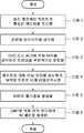
도 1은 본 발명의 일 실시 형태에 따른 Ni 배선의 제조 방법을 개략적으로 나타내는 흐름도이다.
도 2는 본 발명의 일 실시 형태에 따른 Ni 배선의 제조 방법을 개략적으로 나타내는 공정 단면도이다.
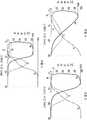
도 3은 환원 가스의 NH3/H2를 변화시켜 니켈 알킬 아미디네이트를 이용한 CVD에 의해 Ni막을 성막한 경우, 및 PVD에 의해 Ni막을 성막한 경우의 TEM 사진이다.
도 4는 환원 가스의 NH3/H2를 변화시켜 니켈 알킬 아미디네이트를 이용한 CVD에 의해 Ni막을 성막한 경우, 및 PVD에 의해 Ni막을 성막한 경우의 성막한 채로(as depo)의 저항율을 나타내는 도면이다.
도 5는 환원 가스의 NH3/H2를 변화시켜 니켈 알킬 아미디네이트를 이용한 CVD에 의해 Ni막을 성막한 경우의 XPS에 의한 막의 깊이 방향의 원소 분석 결과를 나타내는 도면이다.
도 6은 환원 가스의 NH3 가스와 H2 가스의 비율(NH3/H2비)을, 100%/0%, 80%/20%, 50%/50%, 20%/80%의 4종으로 하고, 각각 막 두께를 변화시켜 CVD에 의해 Ni막을 성막한 경우의 막 두께와 저항율의 관계를 나타내는 도면이다.
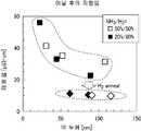
도 7은 환원 가스의 NH3/H2를 변화시켜 니켈 알킬 아미디네이트를 이용한 CVD에 의해 Ni막을 성막한 경우, 및 PVD에 의해 Ni막을 성막하고, 어닐한 후의 저항율을 나타내는 도면이다.
도 8은 환원 가스의 NH3 가스와 H2 가스의 비율(NH3/H2비)을 50%/50%, 20%/80%의 2종으로 하고, 각각 막 두께를 변화시켜 CVD에 의해 Ni막을 성막하고, 어닐한 후의 막 두께와 저항율의 관계를 나타내는 도면이다.
도 9는 Ni막을 성막할 때에, 트렌치의 상부에서 오버행이 생겨 Ni막이 막힌 상태를 모식적으로 나타내는 단면도이다.
도 10은 좁은 폭의 트렌치와 넓은 폭의 트렌치에 대해, 성막과 어닐을 2회 반복하여 트렌치 상부가 막히는 일없이 Ni막을 매립하는 수법을 설명하기 위한 공정 단면도이다.
도 11은 하지의 층간 절연막을 에치백하여 트렌치 상부가 막히는 일없이 Ni막을 매립하는 수법을 설명하기 위한 공정 단면도이다.
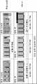
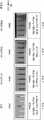
도 12는 실험예 1에 있어서의, Ni 성막시의 각 조건에서의, as depo 상태, 및 어닐한 후의 단면의 TEM 사진이다.
도 13은 실험예 2에 있어서의, as depo 상태, 에치백+성막, 에치백+성막+어닐, 에치백+(성막+어닐)×2의 단면의 TEM 사진이다.
도 14는 실험예 3에 있어서의, 조건 1~4에 의해 형성한 Ni 배선의 단면의 TEM 사진, 실제의 CD의 값 및 저항율의 값을 나타내는 도면이다.
도 15는 실험예 4에서, 실험예 3의 조건 3과 동일한 조건에서, CD를 변경한 경우의 TEM 사진, 실제의 CD의 값 및 저항율의 값을 나타내는 도면이다.
도 16은 Ni 배선의 제조 방법을 실시하기 위해서 이용되는 성막 시스템의 일례를 개략적으로 나타내는 수평 단면도이다.
도 17은 도 16의 성막 시스템에 탑재된 Ni막 성막 장치의 일례를 개략적으로 나타내는 단면도이다.1 is a flowchart schematically showing a method for manufacturing a Ni wiring according to one embodiment of the present invention.
2 is a cross-sectional view schematically illustrating the method of manufacturing the Ni wirings according to the embodiment of the present invention.
FIG. 3 is a TEM photograph when the Ni film is formed by CVD using nickel alkyl amidate by changing NH3 / H2 of the reducing gas, and when the Ni film is formed by PVD.
FIG. 4 shows the resistivity of the Ni film when the Ni film is formed by CVD using nickel alkyl amidate by changing NH3 / H2 of the reducing gas, and when the Ni film is formed by PVD. It is a figure which shows.
Fig. 5 is a diagram showing the results of elemental analysis in the depth direction of a film by XPS when a Ni film is formed by CVD using nickel alkyl amidate by changing NH3 / H2 of the reducing gas.
FIG. 6 shows the ratio (NH3 / H2 ratio) of NH3 gas and H2 gas of reducing gas, 100% / 0%, 80% / 20%, 50% / 50%, 20% / 80%. It is a figure which shows the relationship between the film thickness and resistivity at the time of making a Ni film into a film by CVD, changing a film thickness, respectively.
Fig. 7 is a graph showing the resistivity after forming an Ni film by CVD using nickel alkyl amidate by changing NH3 / H2 of the reducing gas and forming an Ni film by PVD.
Fig. 8 shows the ratio (NH3 / H2 ratio) of NH3 gas and H2 gas of the reducing gas to 50% / 50% and 20% / 80%, and the thicknesses of the reducing gases are respectively changed by CVD. It is a figure which shows the relationship between the film thickness and resistivity after forming a Ni film and annealing.
9 is a cross-sectional view schematically showing a state in which an overhang occurs in the upper portion of the trench and the Ni film is blocked when the Ni film is formed.
FIG. 10 is a cross-sectional view for explaining a method of embedding a Ni film in a narrow trench and a wide trench by repeating film formation and annealing twice without clogging the upper portion of the trench.
Fig. 11 is a cross sectional view for explaining a method of embedding a Ni film without etching the underlying interlayer insulating film to block the upper portion of the trench.
12 is a TEM photograph of a cross section after the as depo state and the annealing in each condition during Ni film formation in Experimental Example 1. FIG.
FIG. 13 is a TEM photograph of a cross section of an as depo state, an etch back + film formation, an etch back + film formation + annealing, and an etch back + (film formation + annealing) x 2 in Experimental Example 2. FIG.
It is a figure which shows the TEM photograph of the cross section of the Ni wiring formed under the conditions 1-4 in Experimental example 3, the value of actual CD, and the value of resistivity.
FIG. 15 is a diagram showing a TEM photograph, a value of an actual CD, and a value of a resistivity when a CD is changed under the same conditions as
FIG. 16 is a horizontal sectional view schematically showing an example of a film forming system used for carrying out a method for manufacturing a Ni wiring. FIG.
17 is a cross-sectional view schematically showing an example of a Ni film forming apparatus mounted on the film forming system of FIG. 16.
이하, 첨부 도면을 참조하여 본 발명의 실시 형태에 대해 구체적으로 설명한다.EMBODIMENT OF THE INVENTION Hereinafter, embodiment of this invention is described concretely with reference to an accompanying drawing.
<Ni 배선의 형성 방법의 개요><Overview of the Ni wiring formation method>
먼저, 본 발명의 일 실시 형태에 따른 Ni 배선의 제조 방법의 개요에 대해 설명한다. 도 1은 본 발명의 일 실시 형태에 따른 Ni 배선의 제조 방법을 개략적으로 나타내는 흐름도, 도 2는 그 공정 단면도이다.First, the outline | summary of the manufacturing method of Ni wiring which concerns on one Embodiment of this invention is demonstrated. BRIEF DESCRIPTION OF THE DRAWINGS The flowchart which shows schematically the manufacturing method of Ni wiring which concerns on one Embodiment of this invention, and FIG.
우선, 소정의 하부 구조(도시 생략)를 가지는 실리콘 등의 반도체로 이루어지는 기체(201) 위에 SiO2막, 저유전율(Low-k)막(SiCO, SiCOH 등) 등으로 이루어지는 층간 절연막(하지막)(202)이 형성되고, 층간 절연막(하지막)(202)에 트렌치(오목부)(203)가 소정 패턴으로 형성된 피처리 기판인 반도체 웨이퍼(이하, 간단히 웨이퍼라고 기재함) W를 준비한다(스텝 1, 도 2(a)).First, an interlayer insulating film (base film) made of a SiO2 film, a low dielectric constant (Low-k) film (SiCO, SiCOH, etc.) or the like on a
다음에, 이 웨이퍼 W에 대해, 필요에 따라, 사전 처리로서 데가스(Degas) 프로세스나 전(前)세정(프리크리; Pre-Clean) 프로세스를 행한 후, 트렌치(203)의 표면을 포함하는 전면(全面)에 Ni의 확산을 억제하는 배리어막(204)을 성막한다(스텝 2, 도 2(b)).Next, the wafer W is subjected to a degas process or a pre-clean process as a pretreatment, if necessary, and then includes the surface of the
배리어막(204)으로서는, Ni에 대해 높은 배리어를 갖고, 저저항의 것이 바람직하며, Ti막, TiN막, Ta막, TaN막 등을 적절히 이용할 수 있다. 배리어막(204)은 물리 증착법(PVD)으로 형성해도, CVD로 형성해도 좋다. Ni는 종래의 배선 재료인 Cu에 비해 확산하기 어렵기 때문에, 배리어막(204)은 Cu 배선의 경우보다 얇아도 좋고, 1㎚ 정도면 충분하다. 조건에 따라서는, 배리어막을 이용하는 일없이 Ni막을 매립하는 것도 가능하다.As the
다음에, 성막 원료 가스와 환원 가스를 이용하여, 배리어막(204)의 형성 후의 웨이퍼에, CVD 또는 원자층 퇴적법(ALD)에 의해 Ni막(205)을 전면에 성막하고, 트렌치(203)를 부분적으로 매립한다(스텝 3, 도 2(c)).Next, using the film forming raw material gas and the reducing gas, the
다음에, 웨이퍼 W에 대해 어닐 처리를 실시하고, 웨이퍼 W 표면 및 트렌치(203) 측벽의 Ni막(205)을 트렌치(203) 내에 리플로우시킨다(스텝 4, 도 2(d)).Next, the wafer W is annealed, and the
다음에, 필요에 따라, 다음의 연마 공정에 대비하여 Ni막의 증가층(206)을 형성한다(스텝 5, 도 2(e)). 증가층(206)은 PVD 또는 CVD에 의해 형성할 수 있다.Next, if necessary, an
다음에, CMP(Chemical Mechanical Polishing)에 의해 웨이퍼 W 표면의 전면을 연마하고, 트렌치(203) 이외의 필드 부분의 증가층(206), Ni막(205), 배리어막(204)을 제거하고, 평탄화한다(스텝 6, 도 2(f)). 이것에 의해, 미세한 Ni 배선(207)을 형성할 수 있다.Next, the entire surface of the wafer W surface is polished by CMP (Chemical Mechanical Polishing) to remove the
또, 트렌치(203)의 바닥부와 기체(201) 상의 하부 구조의 사이에 소정 간격으로 비아 홀이 형성되어 있고, 트렌치(203)와 비아 홀을 동시에 매립하도록 하여도 좋다.In addition, a via hole is formed at a predetermined interval between the bottom of the
다음에, 이상의 공정 중, 주요 공정인 스텝 3 및 스텝 4에 대해 상세히 설명한다.Next,
스텝 3의 성막 공정에서는, 미세한 트렌치에 양호한 스텝 커버리지(coverage)로 Ni막을 형성하기 위해, 성막 수법으로서 CVD 또는 ALD를 이용한다. PVD에서는 스텝 커버리지가 나쁜 경향이 있어, 미세한 트렌치에 매립이 곤란하지만, CVD나 ALD를 이용함으로써, 미세 트렌치 내에 막 형성할 수 있다.In the film forming step of
CVD에 의해 Ni막을 성막하는 경우에는, 성막 원료 가스인 Ni 화합물 가스와 환원 가스를 동시에 웨이퍼 W에 공급하고, ALD에 의해 성막하는 경우에는, 성막 원료 가스의 공급과 환원 가스의 공급을, 웨이퍼 W 상의 잔류 가스의 제거를 사이에 두고 교대로 행한다.In the case of forming a Ni film by CVD, Ni compound gas, which is a film forming raw material gas, and a reducing gas are simultaneously supplied to the wafer W. When forming a film by ALD, the supply of the film forming raw material gas and the supply of the reducing gas are carried out. The residual gas in the phase is removed and alternately disposed.
성막 원료로서 이용하는 Ni 화합물로서는, 니켈 아미디네이트, 예를 들면 니켈 알킬 아미디네이트를 이용할 수 있다. 니켈 알킬 아미디네이트는 적당한 용매(예를 들면 테트라인 용매)에 용해시킨 상태에서 이용할 수 있다. 니켈 알킬 아미디네이트로서는, 니켈(II) N, N'-디테트리부틸아미디네이트, 니켈(II) N, N'-디이소프로필아미디네이트, 니켈(II) N, N'-디에틸아미디네이트, 니켈(II) N, N'-디메틸아미디네이트 등을 들 수 있다. 또한, 다른 Ni 화합물로서는, 비스(시클로펜타디엔일) 니켈, 비스메틸시클로펜타디엔일 니켈, 비스(에틸시클로펜타디엔일) 니켈, 비스(이소프로필시클로펜타디엔일) 니켈, 비스(2, 2, 6, 6-테트라 메틸-3, 5-헤부탄디온산) 니켈(II), 비스(헥사플루오로아세틸아세토나토) 니켈(II), 테트라키스(트리플루오로포스핀) 니켈 등을 들 수 있다. 이상의 Ni 화합물 중에서는 니켈 아미디네이트를 이용하는 것이 바람직하다. 니켈 아미디네이트를 이용하는 것에 의해, 미세한 트렌치에 대해 양호한 스텝 커버리지로 Ni막을 성막할 수 있다. 또한, 니켈 아미디네이트는 웨이퍼 W 표면에 NH3 가스를 존재시킨 경우에, 지극히 양호한 흡착성을 나타낸다.As a Ni compound used as a film-forming raw material, nickel amidate, for example, nickel alkyl amidate, can be used. Nickel alkyl amidate can be used in the state dissolved in a suitable solvent (for example, a tetraine solvent). As nickel alkyl amidate, nickel (II) N, N'- ditritributyl amidate, nickel (II) N, N'- diisopropyl amidate, nickel (II) N, N'-diethyl Amidinate, nickel (II) N, N'- dimethyl amidinate, etc. are mentioned. Moreover, as another Ni compound, bis (cyclopentadienyl) nickel, bismethyl cyclopentadienyl nickel, bis (ethylcyclopentadienyl) nickel, bis (isopropylcyclopentadienyl) nickel, bis (2, 2 , 6, 6-tetramethyl-3, 5-hebutanedioic acid) nickel (II), bis (hexafluoroacetylacetonato) nickel (II), tetrakis (trifluorophosphine) nickel, and the like. have. It is preferable to use nickel amidate among the above Ni compounds. By using nickel amidate, a Ni film can be formed into a film with favorable step coverage with respect to a minute trench. Nickel amidate exhibits extremely good adsorption property when NH3 gas is present on the wafer W surface.
환원 가스로서는, NH3 가스 및 H2 가스를 적절히 이용할 수 있고, 이들을 병용하는 것이 바람직하다. 이 경우에, 환원 가스의 NH3 가스와 H2 가스의 비율을 변화시킴으로써 성막 모르폴로지(입자 직경) 및 저항율이 변화한다. 구체적으로는, NH3 가스가 많으면 모르폴로지가 양호하게(입경도 작게) 되지만, N을 함유하는 불순물이 증가하여 막의 저항율이 높아진다. 한편, NH3 가스가 적으면(H2 가스가 많으면), 막의 불순물은 적고 저항율은 낮아지지만 모르폴로지가 나빠진다. 경우에 따라서는 모르폴로지의 악화에 기인하여 저항율이 상승한다. 미세한 트렌치(203)를 매립하는 Ni막에는 저저항율로 모르폴로지가 허용 범위인 것이 요구되며, NH3 가스와 H2 가스의 비율을 적절히 조정하는 것에 의해, 이들을 채우는 Ni막을 얻는다.As the reducing gas, it is possible to properly use the NH3 gas and H2 gas is preferably used in combination thereof. In this case, film-forming morphology (particle diameter) and resistivity change by changing the ratio of NH3 gas and H2 gas of the reducing gas. Specifically, when the NH3 gas is large, the morphology becomes good (small particle size), but impurities containing N increase, and the resistivity of the film becomes high. On the other hand, when the NH3 gas is small (the H2 gas is large), the impurities in the film are small and the resistivity is low, but the morphology is bad. In some cases, the resistivity increases due to deterioration of morphology. The Ni film embedding the
이러한 점으로부터, 허용 가능한 NH3 가스와 H2 가스의 비율(NH3/H2비)은 유량 비율(체적 비율)로 0.25~4(20%/80%~80%/20%)의 범위이다. 이 범위이면 저항율을 비교적 낮게 할 수 있고, 트렌치폭에 따라서는 모르폴로지도 허용 범위로 할 수 있다. NH3/H2비보다 바람직한 범위는 0.67~4(40%/60%~80%/20%)이다. 이 범위이면, 저저항율과 모르폴로지를 양립시킬 수 있다. 더 바람직하게는 0.67~2.33((40%/60%~70%/30%)이다.From this point of view, the allowable ratio of NH3 gas and H2 gas (NH3 / H2 ratio) is in the range of 0.25 to 4 (20% / 80% to 80% / 20%) in the flow rate ratio (volume ratio). . Within this range, the resistivity can be made relatively low, and depending on the trench width, morphology can also be set within the allowable range. NH3 / H2 ratio more preferable range is 0.67 to 4 (40% / 60% to 80% / 20%). If it is this range, a low resistivity and morphology can be made compatible. More preferably, it is 0.67-2.33 ((40% / 60%-70% / 30%).
도 3은 환원 가스의 NH3/H2를 변화시켜 니켈 알킬 아미디네이트를 이용한 CVD에 의해 Ni막을 성막한 경우(샘플 A~C), 및 PVD에 의해 Ni막을 성막한 경우(샘플 D)(모두 타겟 막 두께 20㎚)의 투과형 전자현미경(TEM) 사진이다. 도 3으로부터, NH3만인 경우는 모르폴로지가 양호하지만, H2의 비율이 높아짐에 따라 모르폴로지가 악화되고 있는 것을 알 수 있다. 도 4는 이 때의 Ni막의 저항율을 나타내는 도면인데, 환원 가스가 NH3만인 샘플 C의 경우는 저항율이 매우 큰데 반해, 샘플 A, B와 같이 H2를 가하는 것에 의해로 저항율을 저하하는 것을 알 수 있다. 도 5는 이 때의 샘플 A~C의 XPS에 의한 막의 깊이 방향의 원소 분석 결과를 나타내는 도면이다. 이 도면에 나타내는 바와 같이, 환원 가스가 NH3만인 샘플 C는 Ni막에 NH3 중의 N이 불순물로서 많이 잔류하고 있는데 반해, NH3/H2비가 1(50%/50%)인 샘플 B는 불순물이 적고, 메탈릭의 막으로 되어 있는 것을 알 수 있다. NH3/H2비가 0.25(20%/80%)인 샘플 A는 Ni막 중의 불순물로서의 N은 적지만, O가 포함되어 있는 것이 확인되었다. 이것은 모르폴로지가 나쁜 것에 기인하는 것이라고 생각되는 것이고, 통상은 NH3가 적을수록 Ni막 중의 불순물은 저하한다. 도 4에 나타내는 바와 같이, 저항율이 샘플 B보다 샘플 A가 높아지고 있는 것은 샘플 A의 Ni막에 O가 포함되어 있기 때문이라고 생각된다.FIG. 3 shows the case where the Ni film is formed by CVD using nickel alkyl amidate by changing NH3 / H2 of the reducing gas (Samples A to C), and when the Ni film is formed by PVD (Sample D) ( All are transmission electron microscope (TEM) photographs with a target film thickness of 20 nm. 3 shows that morphology is good in the case of NH3 alone, but the morphology deteriorates as the ratio of H2 increases. Fig. 4 shows the resistivity of the Ni film at this time. In the case of sample C having only reducing gas of NH3 , the resistivity is very large, but the resistivity is lowered by adding H2 as in samples A and B. Can be. It is a figure which shows the elemental analysis result of the depth direction of the film | membrane by XPS of samples A-C at this time. As shown in the figure, Sample C having a reducing gas of NH3 alone has a large amount of N in NH3 as impurities in the Ni film, whereas Sample B having an NH3 / H2 ratio of 1 (50% / 50%) It turns out that there is little impurity and it becomes a metallic film. Sample A having an NH3 / H2 ratio of 0.25 (20% / 80%) was found to contain O although less N as an impurity in the Ni film. This is considered to be due to bad morphology, and in general, the less NH3 , the less impurities in the Ni film. As shown in FIG. 4, the reason why the sample A is higher in the resistivity than the sample B is considered to be because the Ni film of the sample A contains O.
또한, 도 6은 환원 가스의 NH3 가스와 H2 가스의 비율(NH3/H2비)을 100%/0%, 80%/20%, 50%/50%, 20%/80%의 4종으로 하고, 각각 막 두께를 변화시켜 CVD에 의해 Ni막을 성막한 경우의 막 두께와 저항율의 관계를 나타내는 도면이다. 이 도면에 나타내는 바와 같이, NH3/H2비가 「100%/0%는 NH3/H2비가 80%/20%, 50%/50%, 20%/80%인 경우와 비교하여 높은 것이 확인되었다. 이로부터, 저저항의 막을 얻기 위해서, NH3/H2의 값은 4(80%/20%) 이하가 바람직한 것이 확인되었다.6 shows the ratio (NH3 / H2 ratio) of NH3 gas and H2 gas of the reducing gas to 100% / 0%, 80% / 20%, 50% / 50%, 20% / 80%. It is a figure which shows the relationship between the film thickness and resistivity at the time of forming four types and forming Ni film into a film by CVD by changing film thickness, respectively. As shown in this figure, the NH3 / H2 ratio is " 100% / 0% is higher than when the NH3 / H2 ratio is 80% / 20%, 50% / 50%, 20% / 80%. Confirmed. From this, it was confirmed that the value of NH3 / H2 is preferably 4 (80% / 20%) or less in order to obtain a low resistance film.
스텝 3의 성막 공정은 150~350℃의 범위의 온도에서 행해지는 것이 바람직하다. 이용하는 Ni 화합물에 의해 바람직한 온도 범위는 상이하지만, Ni 화합물로서 니켈 아미디네이트를 이용하는 경우는 150~350℃의 범위가 바람직하다. 또한, 성막시의 압력은 133.32~1333.2㎩(1~10Torr)가 바람직하다.It is preferable that the film-forming process of
스텝 4의 어닐 공정에서는, 어닐시의 열에 의해, 웨이퍼 W 표면 및 트렌치(203) 측벽의 Ni막(205)을 트렌치(203) 내에 리플로우(유동)시킨다. 이와 같이 하지 상에 성막된 Ni막(205)을 어닐에 의해 트렌치 내에 리플로우할 수 있는 점은 본 발명자 등이 처음으로 찾아낸 지견이다. 종래의 Cu 배선의 Cu막은 TiN막 등의 배리어막 상에서 유동하기 어려웠지만, Ni막에서는 배리어막 상에서도 양호한 유동성을 갖고, 리플로우가 가능해진다. 또한, 배리어막을 마련하지 않는 경우에도, 하지의 층간 절연막 상에서 양호한 유동성을 나타낸다. 이와 같이 웨이퍼 W의 표면이나 트렌치 측면의 Ni막을 트렌치(203) 내에 리플로우시키는 것에 의해, 성막한 채로는 매립하는 것이 곤란한 미세 트렌치에서도 양호한 매립성을 확보할 수 있다.In the annealing step of step 4, the
이 어닐 공정의 온도는 200~600℃의 범위, 예를 들면 400℃인 것이 바람직하다. 또한, 어닐 공정의 분위기는 특별히 한정되지 않지만, N2 가스 등의 불활성 분위기로 행할 수 있다. 또한, H2 가스 분위기에서 행할 수도 있다.It is preferable that the temperature of this annealing process is 200-600 degreeC, for example, 400 degreeC. The atmosphere of the annealing step is not particularly limited, and can be carried out in an inert atmosphere such as N2 gas. It may also be carried out at a H2 gas atmosphere.
어닐시의 리플로우 특성은 불순물이 적고 메탈릭한 막인일수록 양호해진다. 반대로, 환원 가스를 NH3 가스만으로 한 경우에 형성되는 불순물이 많은 Ni막의 경우에는, 유동하기 어렵고, 그 자리에서 응집되기 쉽다.The reflow characteristic at the time of annealing becomes better as it is a metallic film with few impurities. On the contrary, in the case of a Ni film with many impurities formed when the reducing gas is made of only NH3 gas, it is difficult to flow and easily aggregate on the spot.
또한, 어닐 처리는, Ni의 결정화를 진행시키고, 또한 불순물을 저감시키는 효과도 있으므로, Ni막의 저항율을 저하시키는 것에도 기여한다. 도 7은 상기 샘플 A~D를 N2 분위기에서 400℃에서 40min 어닐을 실시한 후의 Ni막의 저항율의 값이지만, 도 4와 비교하면, 모든 샘플에서 저항율이 저하하고, 특히, as depo에서 불순물이 많은 샘플 C에서 저항율의 저하가 큰 것을 알 수 있다. 또한, 어닐 후의 저항율의 값 자체는 as depo에서 불순물이 적게 메탈릭한 막인 샘플 B가, 샘플 D의 PVD-Ni막에 가까운 20μΩ·㎝라고 하는 낮은 값을 나타냈다. 도 8은 NH3/H2비가 50%/50%, 20%/80%인 경우에 대해, 각각 막 두께를 변화시켜 CVD에 의해 Ni막을 성막했을 때 및 그 후, H2 분위기에서 600℃에서 10min 어닐했을 때의 저항율을 나타내는 도면이지만, 어느 경우라도 어닐에 의해, 10μΩ·㎝에 가까운 지극히 낮은 값으로 되는 것이 확인되었다.In addition, the annealing treatment also has the effect of advancing the crystallization of Ni and reducing impurities, which also contributes to lowering the resistivity of the Ni film. 7 is compared with the sample, but A ~ D the value of the Ni film resistivity after subjected to 40min annealing at 400 ℃ in N2 atmosphere, and 4, the resistivity decreases in all samples, and in particular, a lot of impurities in the as depo It turns out that the fall of resistivity is large in sample C. In addition, the value of the resistivity after annealing itself showed a low value of 20 μΩ · cm, which was close to the PVD-Ni film of Sample D, as Sample B, which was a metallic film with less impurities in as depo. FIG. 8 shows Ni film deposition by CVD with varying film thicknesses for the case where the NH3 / H2 ratio is 50% / 50% and 20% / 80%, respectively, and thereafter, at 600 ° C. in an H2 atmosphere. Although it is a figure which shows the resistivity at the time of 10-min anneal, it was confirmed by annealing in any case to become the extremely low value near 10 microhm * cm.
또, 어닐을 H2 가스 분위기에서 행함으로써 불순물 제거 효과를 높게 할 수 있지만, 불순물이 비교적 많이 포함되어 있는 막을 H2 가스 분위기에서 어닐하면 응집되기 쉬워지므로 주의를 요한다.Further, by carrying out annealing in H2 gas atmosphere but can be increased to effect removal of impurities, if the impurities are annealed film that contains a relatively large amount in a H2 gas atmosphere so easily aggregated requires attention.
스텝 3의 성막 공정시에, 도 9에 나타내는 바와 같이, 트렌치(203)의 상부에서 오버행이 생겨 Ni막(205)이 차버리면, 트렌치(203)의 바닥부까지 Ni막이 리플로우되기 어려워져, 매립 부분에 결함이 생길 우려가 있기 때문에, 트렌치(203)의 상부가 막히지 않을 정도로 얇게 Ni막(205)을 성막하는 것이 바람직하다. 이 때, 1회로 트렌치(203)를 모두 매립할 수 있는 두께로 Ni막(205)을 성막하는 것이 곤란한 경우나, 미세한 트렌치에 대해 양호한 매립성으로 매립하기 위해서는, 성막과 어닐을 2회 이상 반복하는 것이 바람직하다.As shown in FIG. 9 at the time of the film-forming process of
성막과 어닐을 2회 이상 반복하는 예로서는, 이하와 같은 예를 들 수 있다.Examples of repeating film formation and annealing two or more times include the following examples.
예를 들면, 도 10(a)에 나타내는 바와 같이, 적어도, 좁은 폭(예를 들면 폭이 10~50㎚)의 트렌치(203a)와 넓은 폭(예를 들면 폭이 50~100㎚)의 트렌치(203b)를 가지고 있는 웨이퍼 W에서, 1회째의 Ni막(205)의 성막을 행한 후, 1회째의 어닐에 의해 Ni막(205)을 리플로우시키고, 좁은 폭의 트렌치(203a)를 매립한다(도 10(b)). 이 때, 넓은 폭의 트렌치(203b)는 완전하게는 매립되지 않았다. 다음에, 2회째의 Ni막(205)의 성막을 행하고, 그 후, 2회째의 어닐을 행하여 2회째의 Ni막(205)을 리플로우시켜, 넓은 폭의 트렌치(203b)를 매립한다(도 10(c)). 이렇게 하는 것에 의해, 폭이 다른 트렌치를 트렌치 상부가 막히는 일없이 양호하게 매립할 수 있다.For example, as shown in Fig. 10 (a), at least, the
이 경우에, 1회째의 성막시의 Ni막의 막 두께는 2회째의 성막시의 Ni막의 막 두께보다 작게 하는 것이 바람직하다. 이것에 의해, 1회째의 어닐시의 리플로우에 의해, 좁은 폭의 트렌치(203a)의 상부가 막히는 것을 방지하면서 매립할 수 있고, 2회째의 어닐시의 리플로우에 의해 넓은 폭의 트렌치(203b)를 매립할 수 있다.In this case, the film thickness of the Ni film during the first film formation is preferably smaller than the film thickness of the Ni film during the second film formation. Thereby, it is possible to bury the upper portion of the
또한, 2회째의 Ni막 성막시의 환원 가스의 NH3/H2비는 1회째의 Ni막 성막시의 환원 가스의 NH3/H2비보다 작게 하는 것이 바람직하다. 즉, 2회째의 성막쪽이 1회째의 성막보다 환원 가스 중의 H2 가스의 양을 많이 하는 것이 바람직하다. 이것은 1회째에 성막된 Ni막은 1회째의 어닐에 의해 리플로우되어 좁은 폭의 트렌치(203a)를 매립하는 것이기 때문에, 어느 정도 모르폴로지가 높은 것이 요구되지만, 2회째에 성막된 Ni막은 2회째의 어닐에 의해 리플로우되어 넓은 폭의 트렌치(203b)를 매립하는 것이기 때문에, 1회째보다 모르폴로지가 낮아도 좋으며, H2 가스의 비율을 높여 저저항화를 도모하는 것이 바람직하기 때문이다.Further, NH3 / H2 ratio of the reducing gas at the time of the second Ni film formed is preferably smaller than the NH3 / H2 in the reducing gas at the time of the first time Ni film deposition ratio. That is, it is preferable that the2nd film-forming side makes more amount of H2 gas in reducing gas than the 1st film-forming. This is because the Ni film formed at the first time is reflowed by the first annealing to fill the
또한, 이상과 같이, 성막과 어닐을 2회 이상 반복하는 것에 의해, Ni막에 어닐이 2회 이상 실시되어, Ni막의 저항율을 더 저감시키는 효과가 도모된다.In addition, by repeating the film formation and the annealing two or more times as described above, the Ni film is subjected to the annealing two or more times, thereby achieving the effect of further reducing the resistivity of the Ni film.
트렌치(203)의 상부에서 Ni막(205)가 막아 버리는 것을 방지하는 수법으로서는, 상술한 성막과 어닐을 2회 이상 반복하는 것 외에, Ni막의 성막에 앞서 기초의 층간 절연막(하지막)(202)을 에치백하는 것도 유효하다. 즉, 도 11(a)과 같이, 층간 절연막(하지막)(202)에 트렌치(203)가 형성되어 있는 상태에서, 트렌치(203)에 돌출부(210)가 형성되는 일이 있지만, 하지의 층간 절연막(하지막)(202)를 에치백함으로써, 도 11(b)과 같이, 트렌치(203)의 돌출부(210)가 에칭되어 트렌치(203)의 폭이 넓어지고, 도 11(c)과 같이, Ni막(205)을 매립할 때에, 트렌치(203)의 상부에서 오버행이 생기는 것이 방지된다.As a method of preventing the
또한, 하지의 층간 절연막(하지막)(202)를 에치백하는 것과, 성막 및 어닐을 2회 이상 반복하는 것의 양쪽을 행하여도 좋다. 이것에 의해, 트렌치(203)의 상부에서 Ni막(205)이 막아 버리는 것을 보다 유효하게 억제할 수 있다.It is also possible to etch back the underlying interlayer insulating film (base film) 202 and to repeat the film formation and annealing two or more times. This can more effectively suppress the
이상과 같이, 본 실시 형태에서는, CVD 또는 ALD에 의해 Ni막(205)을 성막한 후, 성막한 Ni막(205)을 어닐에 의해 트렌치(203) 내에 리플로우시키므로, 미세한 트렌치를 매립하여 Ni 배선을 형성할 수 있다. Ni는 전자의 평균 자유 행정이 Cu보다 훨씬 짧기 때문에, 미세 배선을 Ni 배선으로 함으로써, Cu 배선보다 저항율을 낮게 하는 것이 가능하게 된다. 또한, Ni 배선은 Cu 배선에서 필요한 배리어막이나 라이너막을 없앨 수 있어, 배리어막이 필요한 경우이더라도 Cu 배선의 경우보다 얇게 할 수 있으므로, 배선 중의 Ni막의 체적을 크게 할 수 있고, 배선을 보다 저저항으로 할 수 있다.As described above, in the present embodiment, after the
또한, CVD 또는 ALD에 의해 Ni막(205)을 성막하는 경우에, Ni 화합물 가스를 환원하는 환원 가스로서 NH3 가스 및 H2 가스를 이용하는 것에 의해, 이들 비율에 의해 막의 모르폴로지와 불순물량을 조정할 수 있어, 미세한 트렌치(203)에 저저항의 Ni막을 결함없이 매립할 수 있다.In the case of forming the
또, Ni 화합물 가스로서 니켈 아미디네이트를 이용하는 것에 의해, 미세한 트렌치에 대해 양호한 스텝 커버리지로 Ni막을 성막할 수 있어, 보다 양호한 매립성을 얻을 수 있다.Moreover, by using nickel amidate as the Ni compound gas, the Ni film can be formed into a film with good step coverage with respect to fine trenches, and better embedding properties can be obtained.
<실험예>Experimental Example
이하 실험예에 대해 설명한다.An experimental example is described below.
[실험예 1]Experimental Example 1
여기서는, Si기체 상에, 테트라에틸오르소실리케이트(TEOS)를 이용한 CVD에 의해 SiO2막을 형성하고, 이 SiO2막에 실제의 CD(미들 CD)가 30~150㎚, 깊이 200㎚의 트렌치를 복수 형성한 웨이퍼를 준비하였다.Here, a SiO2 film is formed on the Si gas by CVD using tetraethylorthosilicate (TEOS), and the actual CD (middle CD) of 30 to 150 nm and a depth of 200 nm is formed on the SiO2 film. A plurality of wafers were prepared.
이러한 구조의 웨이퍼에 대해, CVD에 의해 두께 1㎚의 TiN막으로 이루어지는 배리어막을 성막한 후, 두께 20㎚의 Ni막을 성막하였다. Ni막은 성막 원료인 Ni 화합물로서 니켈 알킬 아미디네이트를 이용하여 환원 가스로서 NH3 가스 및 H2 가스를 이용해서 250℃에서 성막하였다. 환원 가스는 NH3/H2비를 20%/80%, 50%/50%, 100%0%(NH3만)의 3종류로 하였다. 그 후, N2 가스 분위기에서 400℃에서 40min의 어닐 처리를 실시해서, Ni막을 리플로우시켰다.On the wafer having such a structure, a barrier film made of a TiN film having a thickness of 1 nm was formed by CVD, and then a Ni film having a thickness of 20 nm was formed. Ni deposition film as a raw material, a reducing gas using a nickel alkyl amidinyl carbonate as a Ni compound using the NH3 gas and H2 gas was formed at 250 ℃. The reducing gas was composed ofthree types of NH3 / H2 ratios of 20% / 80%, 50% / 50%, and 100% 0% (NH3 only). Thereafter, annealing was performed at 400 ° C. for 40 min in an N2 gas atmosphere to reflow the Ni film.
도 12에, 성막한 채의(as depo) 상태 및 어닐 후의 단면의 TEM 사진을 나타낸다. 이들 사진에 나타내는 바와 같이, as depo 상태에서는, NH3 가스의 비율이 높아질수록 막의 모르폴로지는 양호하게 되지만, 모두 트렌치 내에 심이 남아, 결함이 없는 매립을 할 수 없었다(도 12(a)). 이에 반해, 성막 후 어닐하여 Ni막을 리플로우시킨 경우는 NH3/H2비가 20%/80% 및 NH3 가스만에서는 트렌치 내에 보이드가 생겼지만, NH3/H2비가 50%/50%인 경우는 양호한 매립성이 얻어졌다(도 12(b)). 이것은 NH3/H2비가 20%/80%에서는 모르폴로지가 나쁘고, NH3 가스만에서는 불순물이 많은데 반해, NH3/H2비가 50%/50%인 경우에는, 모르폴로지가 허용 범위이고, 또한 불순물이 적기 때문이라고 생각된다.In FIG. 12, the TEM photograph of the cross section after annealing and annealing is shown. As shown in these photographs, in the as depo state, as the ratio of NH3 gas is increased, the morphology of the membrane becomes better, but all of the seams remain in the trenches, and no defects can be buried (Fig. 12 (a)). In contrast, when the Ni film was reflowed after annealing, the NH3 / H2 ratio was 20% / 80%, and only the NH3 gas had voids in the trench, but the NH3 / H2 ratio was 50% / 50%. In the case, good embedding properties were obtained (Fig. 12 (b)). This is because the morphology is bad at the NH3 / H2 ratio of 20% / 80%, and the impurity is high only in the NH3 gas, whereas when the NH3 / H2 ratio is 50% / 50%, the morphology is an acceptable range, It is also considered that there are few impurities.
[실험예 2]Experimental Example 2
여기서는, Si 기체 상에, TEOS를 이용한 CVD에 의해 SiO2막을 형성하고, 이 SiO2막에 실제의 CD(미들 CD)가 30~150㎚, 깊이 200㎚의 트렌치를 복수 형성한 웨이퍼를 준비하였다.Here, a SiO2 film was formed on a Si substrate by CVD using TEOS, and a wafer in which a plurality of trenches having an actual CD (middle CD) of 30 to 150 nm and a depth of 200 nm was formed on the SiO2 film. .
이러한 구조의 웨이퍼에 대해, CVD에 의해 두께 1㎚의 TiN막으로 이루어지는 배리어막을 성막하고, 또 두께 20㎚의 Ni막을 성막하였다. Ni막은 성막 원료인 Ni 화합물로서 니켈 알킬 아미디네이트를 이용하고, 환원 가스로서 NH3 가스 및 H2 가스를 이용하여 NH3/H2비를 50%/50%, 100%0%(NH3만)의 2종류로 하고, 250℃에서 성막하였다.On the wafer having such a structure, a barrier film made of a TiN film having a thickness of 1 nm was formed by CVD, and a Ni film having a thickness of 20 nm was formed. Ni film uses nickel alkyl amidate as the Ni compound as the raw material for film formation, and the NH3 / H2 ratio is 50% / 50% and 100% 0% (NH3) by using NH3 gas and H2 gas as reducing gas. Film) at 250 ° C.
또한, 막 형성에 앞서, SiO2막의 에치백을 행하고(에칭 가스: C4F8, O2, Ar), 트렌치의 폭을 넓힌 후, CVD에 의해 두께 1㎛의 TiN막으로부터 되는 배리어막을 성막하고, 두께 30㎚로 한 Ni막을 성막한 샘플도 더 제작하였다. 이 때의 Ni막의 성막 조건은 상기 조건과 동일하게 하였다.In addition, prior to film formation, an etching back of the SiO2 film is performed (etching gas: C4 F8 , O2 , Ar), the width of the trench is widened, and a barrier film made of a TiN film having a thickness of 1 μm is formed by CVD. And the sample which formed the Ni film into a film 30nm thick was further produced. The film forming conditions of the Ni film at this time were the same as the above conditions.
이 에치백을 행한 샘플에 대해서는, Ni막을 성막한 후, N2 가스 분위기에서 400℃에서 40min의 어닐 처리를 실시하고, Ni막을 리플로우시켰다.About the sample which etched back, after forming a Ni film, it annealed for 40 minutes at 400 degreeC in N2 gas atmosphere, and the Ni film was reflowed.
또, 막 형성에 앞서, SiO2막의 에치백을 실시하고(에칭 가스: C4F8, O2, Ar), 트렌치의 폭을 넓힌 후, CVD에 의해 두께 1㎚의 TiN막으로 이루어지는 배리어막을 성막하고, 또 환원 가스의 NH3/H2비를 50%/50%의 조건으로 한정하고, 두께 20㎚로 한 Ni막의 성막과, 상기와 동일한 조건의 어닐 처리를 2회 반복한 샘플도 제작하였다.In addition, prior to film formation, an etching back of the SiO2 film is performed (etching gas: C4 F8 , O2 , Ar), the width of the trench is widened, and a barrier film made of a TiN film having a thickness of 1 nm is formed by CVD. Forming a film, limiting the NH3 / H2 ratio of the reducing gas to a condition of 50% / 50%, and forming a Ni film having a thickness of 20 nm and a sample of repeating annealing treatment under the same conditions as described above twice are also produced. It was.
도 13에, 이들 샘플의 단면의 TEM 사진을 나타낸다. 이러한 사진에 나타내는 바와 같이, as depo 상태에서는, 모두 트렌치 내에 심이 남아, 결함이 없는 매립을 할 수 없었다(도 13(a)). 이에 반해, 에치백한 후, 성막한 경우에는, 환원 가스가 NH3 가스만에서는, 모르폴로지가 양호하기 때문에, 성막한 단계에서 양호한 매립이 달성되었지만, NH3/H2비가 50%/50%에서는, 성막한 단계에서 명확한 심은 볼 수 없기는 하지만, 결함이 잔존하고 있었다(도 13(b)). 또한, 그 후 어닐 처리를 행하는 것으로, 환원 가스가 NH3 가스만에서는, 트렌치 상부에서 Ni의 응집이 생겼다. 한편, NH3/H2비가 50%/50%에서는, 어닐 처리에 의해 Ni가 트렌치 내에 리플로우되어 CD가 50㎚이하의 트렌치는 양호한 매립성으로 매립되었지만, 그것을 넘는 CD의 트렌치는 충분히 매립할 수 없었다(도 13(c)). 또, 성막시에 환원 가스의 NH3/H2비를 50%/50%의 조건으로 한정하고, 20㎚의 성막과 어닐을 2회 반복한 경우에는, 모든 트렌치를 결함이 존재하지 않는 양호한 매립성으로 묻을 수 있었다(도 13(d)).13, the TEM photograph of the cross section of these samples is shown. As shown in this photograph, in the as-depo state, all of the seams remained in the trenches, and no fillings without defects could be made (Fig. 13 (a)). On the other hand, when the film was formed after etching back, since the morphology was good only when the reducing gas was NH3 gas, a good landfill was achieved in the film forming step, but the NH3 / H2 ratio was 50% / 50%. In the film formation step, although no clear seam was seen, defects remained (Fig. 13 (b)). In addition, by performing annealing after that, when the reducing gas was only NH3 gas, aggregation of Ni occurred in the upper portion of the trench. On the other hand, when the NH3 / H2 ratio is 50% / 50%, Ni is reflowed into the trench by annealing so that a trench of 50 nm or less is buried in good embedding, but the trench of the CD exceeding it is sufficiently buried. It could not (Fig. 13 (c)). In addition, when the NH3 / H2 ratio of the reducing gas is limited to 50% / 50% at the time of film formation, and the film formation and annealing are repeated twice at 20 nm, all the trenches are satisfactorily filled with no defects. It could be buried as a castle (Fig. 13 (d)).
[실험예 3]Experimental Example 3
여기서는, 복수의 조건에서 실제로 Ni 배선을 형성한 경우의 저항율 측정 결과에 대해 설명한다.Here, the result of resistivity measurement when Ni wiring is actually formed under several conditions is demonstrated.
소정의 하부 구조를 가지는 Si 기체 상에, TEOS를 이용한 CVD에 의해 SiO2막을 형성하고, 이 SiO2막에 실제의 CD(미들 CD)가 약 30㎚의 트렌치를 복수 형성한 웨이퍼를 준비하였다. 이러한 구조의 웨이퍼에 대해, CVD에 의해 두께 1㎚의 TiN막으로 이루어지는 배리어막을 성막하고, 다음에 여러 조건에서 Ni막의 매립을 행하고, 다음에 PVD에 의해 두께 100㎚의 Ni막의 증가층을 형성한 후, CM를 3분간 행하였다.On a Si substrate having a predetermined substructure, a SiO2 film was formed by CVD using TEOS, and a wafer in which a plurality of trenches having about 30 nm of actual CD (middle CD) were formed on the SiO2 film was prepared. On the wafer having such a structure, a barrier film made of a TiN film having a thickness of 1 nm was formed by CVD, and then a Ni film was buried under various conditions, and then an increase layer of a Ni film having a thickness of 100 nm was formed by PVD. Then, CM was performed for 3 minutes.
Ni막의 매립은 성막 원료인 Ni 화합물로서 니켈 알킬 아미디네이트를 이용하여 환원 가스의 NH3/H2비를 50%/50%로 하고, 두께 30㎚ 성막하고, 어닐은 행하지 않은 것(조건 1), Ni막을 동일한 조건에서 성막한 후, N2 가스 분위기에서 400℃에서 40min의 어닐 처리를 실시한 것(조건 2), 동일한 조건에서의 두께 20㎚의 Ni막의 성막과, 동일한 조건에서 어닐 처리를 2회 반복한 것(조건 3), 환원 가스를 NH3 가스만으로 하고, 두께 30㎚ 성막하고, 어닐은 행하지 않은 것(조건 4)의 4가지의 조건에서 행하였다. 이들에 대해 저항율을 측정하였다.The Ni film was embedded using Ni alkyl amidate as a Ni compound as a film raw material, and the NH3 / H2 ratio of the reducing gas was 50% / 50%, and a thickness of 30 nm was formed without annealing (
도 14에, 이들 조건에 의해 형성한 Ni 배선의 단면의 TEM 사진, 및 이들의 실제의 CD의 값 및 저항율의 값을 나타낸다. 이들 사진에 나타내는 바와 같이, 조건 1에서는 매립성이 충분하지 않고, 저항율이 45.8μΩ·㎝로 높은 값을 나타냈다. 이에 반해, 어닐에 의한 리플로우를 행한 조건 2에서는, 매립성이 조건 1보다 개선되고, 저항율도 23.6μΩ·㎝까지 저하하였다. 또한, 성막과 어닐에 의한 리플로우를 2회 반복한 조건 3에서는, 트렌치 바닥부에 작은 보이드를 볼 수 있었지만, 저항율이 21.1μΩ·㎝로 가장 낮았다. 환원 가스로서 NH3 가스만을 이용하여 Ni막을 성막한 조건 4에서는, CM에 의해 트렌치 내의 Ni의 로스가 생겨, 저항율을 측정할 수 없었다.In FIG. 14, the TEM photograph of the cross section of the Ni wiring formed by these conditions, and the value of these actual CD and the value of resistivity are shown. As shown in these photographs, in the
[실험예 4]Experimental Example 4
여기서는, CD를 변화시켜 실제로 Ni 배선을 형성gks 경우의 저항율 측정 결과에 대해 설명한다.Here, the resistivity measurement result in the case where CD is changed to actually form Ni wirings will be described.
실험예 3과 마찬가지로, 소정의 하부 구조를 가지는 Si 기체 상에, TEOS를 이용한 CVD에 의해 SiO2막을 형성하고, 이 SiO2막에 CD를 바꾸어 복수의 트렌치를 형성한 복수의 웨이퍼를 준비하였다. 각 웨이퍼의 트렌치의 CD는 53㎚, 41㎚, 35㎚, 30㎚로 하였다. 이들 웨이퍼에 대해, CVD에 의해 두께 1㎚의 TiN막으로 이루어지는 배리어막을 성막하고, 다음에 상기 실험예 3의 조건 3과 동일한 조건에서 성막과 어닐에 의한 리플로우를 2회 반복해서 Ni막의 매립을 행하고, 다음에 PVD에 의해 두께 100㎚의 Ni막의 증가층을 형성한 후, CM를 3분간 행하였다. 이들에 대해 저항율을 측정했다.Similarly to
도 15에, 이들 조건에 의해 형성한 Ni 배선의 단면의 TEM 사진, 및 이들의 실제의 CD의 값 및 저항율의 값을 나타낸다. 이들 사진에 나타내는 바와 같이, CD가 35㎚ 이상에서는, 양호한 매립성이 얻어지고, 저항율도 약 15μΩ·㎝로 낮은 값이 얻어졌다. CD가 30㎚인 경우에는, 트렌치 바닥부에 작은 보이드가 보이고, 저항율이 21.1μΩ·㎝로 조금 높은 값으로 되었다. 이러한 결과로부터, Ni막의 매립 조건을 더 조정하여 최적화하는 것에 의해, CD가 30㎚ 이하에서도 양호한 매립성으로 Ni막을 매립하고, 15μΩ·㎝ 정도의 낮은 저항율로 되는 것이 기대된다.In FIG. 15, the TEM photograph of the cross section of the Ni wiring formed by these conditions, and the value of these actual CD and the value of resistivity are shown. As shown in these photographs, when the CD was 35 nm or more, good embedding properties were obtained, and a low resistivity of about 15 μΩ · cm was obtained. When CD was 30 nm, a small void was seen in the trench bottom part, and the resistivity became a slightly high value of 21.1 micro-ohm-cm. From these results, by further adjusting and optimizing the embedding conditions of the Ni film, it is expected that the Ni film is buried with good embedding even when the CD is 30 nm or less, resulting in a low resistivity of about 15 µΩ · cm.
<성막 시스템>Film Formation System
다음에, 상술한 Ni 배선의 제조 방법을 실시하기 위해 이용되는 성막 시스템의 일례에 대해 설명한다.Next, an example of the film-forming system used for implementing the manufacturing method of Ni wiring mentioned above is demonstrated.
도 16은 성막 시스템의 일례를 개략적으로 나타내는 수평 단면도이다.16 is a horizontal cross-sectional view schematically showing an example of a film forming system.
도 16에 나타내는 바와 같이, 본 예의 성막 시스템(300)은 평면 형상이 칠각형을 이루는 진공 반송실(301)을 갖고, 진공 반송실(301)의 4개의 벽부에 각각 게이트 밸브 G를 거쳐서 TiN막 성막 장치(302), Ni막 성막 장치(303), 어닐 장치(304), 및 증가층 형성 장치(305)가 접속되어 있다. TiN막 성막 장치(302)는 CVD 또는 ALD에 의해 배리어막으로서의 TiN막을 성막하는 것이다. Ni막 성막 장치(303)는 CVD 또는 ALD에 의해 트렌치를 매립하기 위한 Ni막을 성막하는 것이다. 어닐 장치(304)는 Ni막 성막 후에 웨이퍼를 어닐하여 Ni막을 트렌치 내에 리플로우하기 위한 것이다. 증가층 형성 장치(305)는 매립을 위한 Ni막 위에 PVD 또는 CVD에 의해 다음의 CMP 처리에 대비하여 Ni막의 증가층을 더 형성하기 위한 것이다. 진공 반송실(301) 내는 진공 펌프에 의해 배기되어 소정의 진공도로 유지된다.As shown in FIG. 16, the film-forming
또한, 진공 반송실(301)의 다른 3개의 벽부에는 3개의 로드록실(306)이 게이트 밸브 G1을 거쳐서 접속되어 있다. 로드록실(306)을 사이에 두고 진공 반송실(301)의 반대측에는 대기 반송실(307)이 마련되어 있다. 3개의 로드록실(306)은 게이트 밸브 G2를 거쳐서 대기 반송실(307)에 접속되어 있다. 로드록실(306)은 대기 반송실(307)과 진공 반송실(301)의 사이에서 웨이퍼 W를 반송할 때에, 대기압과 진공의 사이에서 압력 제어하는 것이다.In addition, three
대기 반송실(307)의 로드록실(306) 설치벽부와는 반대측의 벽부에는 웨이퍼 W를 수용하는 캐리어(FOUP 등) C를 설치하는 3개의 캐리어 설치 포트(308)를 가지고 있다. 또한, 대기 반송실(307)의 측벽에는, 웨이퍼 W의 얼라인먼트를 행하는 얼라인먼트 챔버(309)가 마련되어 있다. 대기 반송실(307) 내에는 청정 공기의 다운플로우가 형성되도록 되어 있다.The wall part on the opposite side to the
진공 반송실(301) 내에는, 웨이퍼 반송 기구(310)가 마련되어 있다. 웨이퍼 반송 기구(310)는 TiN막 성막 장치(302), Ni막 성막 장치(303), 어닐 장치(304), 증가층 형성 장치(305), 및 로드록실(306)에 대해 웨이퍼 W를 반송한다. 웨이퍼 반송 기구(310)는 독립적으로 이동 가능한 2개의 반송 암(310a, 310b)을 가지고 있다.In the
대기 반송실(307) 내에는, 웨이퍼 반송 기구(311)가 마련되어 있다. 웨이퍼 반송 기구(311)는 캐리어 C, 로드록실(306), 얼라인먼트 챔버(309)에 대해 웨이퍼 W를 반송하도록 되어 있다.In the
성막 시스템(300)은 전체 제어부(312)를 가지고 있다. 전체 제어부(312)는 TiN막 성막 장치(302), Ni막 성막 장치(303), 어닐 장치(304), 증가층 형성 장치(305)의 각 구성부, 진공 반송실(301)의 배기 기구나 웨이퍼 반송 기구(310), 로드록실(306)의 배기 기구나 가스 공급 기구, 대기 반송실(307)의 웨이퍼 반송 기구(311), 게이트 밸브 G, G1, G2의 구동계 등을 제어하는, CPU(컴퓨터)를 가지는 주제어부와, 입력 장치(키보드, 마우스 등), 출력 장치(프린터 등), 표시 장치(디스플레이 등), 기억 장치(기억 매체)를 가지고 있다. 전체 제어부(312)의 주제어부는, 예를 들면 기억 장치에 내장된 기억 매체, 또는 기억 장치에 세트된 기억 매체에 기억된 처리 레시피에 근거하여, 성막 시스템(300)으로 하여금 소정의 동작을 실행시킨다. 또한, 전체 제어부(312)는 도시하고 있지 않은 CMP 장치도 제어하도록 되어 있다.The
또, 성막 시스템(300)과 CMP 장치에 의해, Ni 배선 제조 시스템을 구성한다.Moreover, the Ni wiring manufacturing system is comprised by the film-forming
다음에, 성막 시스템(300)에서 중심으로 되는 Ni막 성막 장치(303)에 대해 설명한다.Next, the Ni film-forming
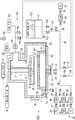
도 17은 Ni막 성막 장치(303)의 일례를 나타내는 단면도이다. 이 Ni막 성막 장치(303)는 기밀하게 구성된 대략 원통형의 챔버(1)를 가지고 있고, 그 중에는 피처리 기판인 웨이퍼 W를 수평으로 지지하기 위한 서셉터(2)가, 후술하는 배기실의 바닥부로부터 그 중앙 하부에 이르는 원통형의 지지 부재(3)에 의해 지지된 상태로 배치되어 있다. 이 서셉터(2)는, 예를 들면 AlN 등의 세라믹스로 이루어져 있다. 또한, 서셉터(2)에는 히터(5)가 내장되어 있고, 이 히터(5)에는 히터 전원(6)이 접속되어 있다. 한편, 서셉터(2)의 상면 근방에는 열전대(7)가 마련되어 있고, 열전대(7)의 신호는 히터 콘트롤러(8)에 전송되도록 되어 있다. 그리고, 히터 콘트롤러(8)는 열전대(7)의 신호에 따라 히터 전원(6)에 지령을 송신하고, 히터(5)의 가열을 제어하여 웨이퍼 W를 소정의 온도로 제어하도록 되어 있다. 서셉터(2)의 내부의 히터(5)의 위쪽에는 고주파 전력 인가용의 전극(27)이 매설립되어 있다. 이 전극(27)에는 정합기(28)를 거쳐서 고주파 전원(29)이 접속되어 있고, 필요에 따라 전극(27)에 고주파 전력을 인가하여 플라스마를 생성하고, 플라스마 CVD를 실시하는 것도 가능하게 되어 있다. 또, 서셉터(2)에는 3개의 웨이퍼 승강 핀(도시하지 않음)이 서셉터(2)의 표면에 대해 돌출 가능하게 마련되어 있고, 웨이퍼 W를 반송할 때에, 서셉터(2)의 표면으로부터 돌출한 상태로 된다. 또한, 서셉터(2)는 승강 기구(도시하지 않음)에 의해 승강 가능하게 되어 있다.17 is a cross-sectional view showing an example of the Ni
챔버(1)의 바닥벽에는, 아래쪽으로 향해 돌출하는 배기실(21)이 마련되어 있다. 챔버(1) 내는 배기실(21)을 거쳐서 배기 기구(20)에 의해 배기되도록 되어 있다. 배기 기구(20)는 배기실(21)의 측면에 접속된 배기 배관(22)과, 배기 배관(22)에 개재된, 챔버(1) 내의 압력을 제어하기 위한 자동 압력 제어 밸브(APC)(23)와, 배기 배관(22)를 거쳐서 챔버(1) 내를 배기하기 위한 진공 펌프(24)를 가지고 있다.The
챔버(1)의 측벽에는, 웨이퍼 W의 반입출을 행하기 위한 반입출구(25)가 형성되어 있고, 이 반입출구(25)는 게이트 밸브 G를 거쳐서 진공 반송실(301)과 접속되어 있다.A carry-in / out
챔버(1)의 천벽(1a)에는, 원형의 구멍(1b)이 형성되어 있고, 그곳으로부터 챔버(1) 내로 돌출하도록 샤워 헤드(10)가 감입되어 있다. 샤워 헤드(10)는 후술하는 가스 공급 기구(30)로부터 공급된 성막용의 가스를 챔버(1) 내에 토출하기 위한 것이고, 그 상부에는, 성막 원료 가스인 니켈 화합물 가스를 도입하는 제 1 도입로(11)와, 환원 가스로서의 NH3 가스 및 H2 가스를 도입하는 제 2 도입로(12)를 가지고 있다. 샤워 헤드(10)는 베이스 부재(13)와, 샤워 플레이트(14)와, 베이스 부재(13)와 샤워 플레이트(14)의 사이에 마련된 원통형의 측벽(15)을 가지고 있고, 내부에 가스 확산 공간(16)이 형성되어 있다. 샤워 플레이트(14)에는 복수의 가스 토출 구멍(17)이 형성되어 있다. 샤워 헤드(10)는 히터(도시하지 않음)에 의해 가열되도록 되어 있다.The
가스 공급 기구(30)는 성막 원료로서, 상술한 바와 같은 Ni 화합물을 저장하는 성막 원료 탱크(31)를 가지고 있다. 성막 원료 탱크(31)에는, Ni 화합물로서 예를 들면 니켈 알킬 아미디네이트가 적당한의 용매(예를 들면 테트라인 용매)에 용해시킨 상태에서 저장되어 있다. 성막 원료 탱크(31)의 주위에는 히터(31a)가 마련되어 있고, 성막 원료 탱크(31) 내의 성막 원료를 적당한 온도로 가열할 수 있도록 되어 있다. 또, 니켈 함유 화합물로서 상온에서 액체인 것을 이용할 때는 용매에 녹이는 일없이 그대로 저장할 수 있다.The
성막 원료 탱크(31)에는, 위쪽으로부터 버블링 가스인 Ar 가스를 공급하기 위한 버블링 배관(32)이 성막 원료에 침지되도록 하여 삽입되어 있다. 버블링 배관(32)에는 Ar 가스 공급원(33)이 접속되어 있고, 또한, 유량 제어기로서의 매스플로우 콘트롤러(34) 및 그 전후의 밸브(35)가 개재되어 있다. 또한, 성막 원료 탱크(31) 내에는 원료 가스 송출 배관(36)이 위쪽으로부터 삽입되어 있고, 이 원료 가스 송출 배관(36)의 타단은 샤워 헤드(10)의 제 1 도입로(11)에 접속되어 있다. 원료 가스 송출 배관(36)에는 밸브(37)가 개재되어 있다. 또한, 원료 가스 송출 배관(36)에는 성막 원료 가스의 응축 방지를 위한 히터(38)가 마련되어 있다. 그리고, 버블링 가스인 Ar 가스가 성막 원료에 공급되는 것에 의해 성막 원료 탱크(31) 내에서 성막 원료가 버블링에 의해 기화되고, 생성된 성막 원료 가스가 원료 가스 송출 배관(36) 및 제 1 도입로(11)를 거쳐서 샤워 헤드(10) 내에 공급된다.The bubbling
버블링 배관(32)과 원료 가스 송출 배관(36)의 사이는 바이패스 배관(48)에 의해 접속되어 있고, 이 배관(48)에는 밸브(49)가 개재되어 있다. 버블링 배관(32) 및 원료 가스 송출 배관(36)에서의 배관(48)의 접속 부분의 하류측에는 각각 밸브(35a, 37a)가 개재되어 있다. 그리고, 밸브(35a, 37a)를 닫고 밸브(49)를 여는 것에 의해, Ar 가스 공급원(33)으로부터의 아르곤 가스를, 버블링 배관(32), 바이패스 배관(48), 원료 가스 송출 배관(36)을 거쳐서, 퍼지 가스 등으로서 챔버(1) 내에 공급하는 것이 가능하게 되어 있다. 또, Ar 가스 대신에 N2 가스 등의 다른 불활성 가스를 이용해도 좋다.The bubbling
샤워 헤드(10)의 제 2 도입로(12)에는 배관(40)이 접속되어 있고, 배관(40)에는 밸브(41)가 마련되어 있다. 이 배관(40)은 분기 배관(40a, 40b)으로 분기하고 있고, 분기 배관(40a)에는 NH3 가스 공급원(42)이 접속되고, 분기 배관(40b)에는 H2 가스 공급원(43)이 접속되어 있다. 또, 분기 배관(40a)에는 유량 제어기로서의 매스플로우 콘트롤러(44) 및 그 전후의 밸브(45)가 개재되어 있고, 분기 배관(40b)에는 유량 제어기로서의 매스플로우 콘트롤러(46) 및 그 전후의 밸브(47)가 개재되어 있다. 배관(40)에는 Ar 가스 배관(51)이 접속되고, Ar 가스 배관(51)에는 퍼지 가스 등으로서 Ar 가스를 공급하는 Ar 가스 공급원(52)이 접속되어 있다. Ar 가스 배관(51)에는 유량 제어기로서의 매스플로우 콘트롤러(53) 및 그 전후의 밸브(54)가 개재되어 있다. 또, Ar 가스 대신에 다른 불활성 가스를 이용해도 좋다.A
필요에 따라 전극(27)에 고주파 전력을 인가하여 플라스마 CVD를 실시하는 경우에는, Ar 가스 공급원(52)으로부터 공급되는 Ar 가스를 플라스마 착화용으로서 이용할 수 있다.When plasma CVD is performed by applying high frequency power to the
원료 가스 송출 배관(36)에는 제 1 프리플로우 라인(61)이 접속되어 있고, 배관(40)에는 제 2 프리플로우 라인(62)이 접속되어 있다. 이들 제 1 및 제 2 프리플로우 라인(61, 62)은 배기관(22)에 접속되어 있고, 원료 가스인 Ni 화합물 가스 및 환원 가스를 챔버(1)를 거치지 않고 배기하는 프리플로우를 행하도록 되어 있다. 제 1 프리플로우 라인(61)에는, 배관(40)측과 배기관(22)측에 각각 밸브(63, 64)가 마련되어 있고, 제 2 프리플로우 라인(62)에는, 배관(40)측과 배기관(22)측에 각각 밸브(65, 66)가 마련되어 있으며, 이들에 의해, 프리플로우와 챔버(1)로의 공급을 전환하도록 되어 있다.The
이상과 같이 구성된 성막 시스템(300)에서는, 도 2(a)에 나타내는 바와 같은 소정의 하부 구조(도시 생략)를 가지는 기체(201) 위에 층간 절연막(하지막)(202)이 형성되고, 층간 절연막(하지막)(202)에 트렌치(오목부)(203)가 소정 패턴으로 형성된 웨이퍼 W를 소정 매수 수용한 캐리어 C를 대기 반송실(307)의 캐리어 설치 포트(308)에 접속한다. 그리고, 우선 웨이퍼 반송 기구(311)에 의해 캐리어 C로부터 웨이퍼 W를 꺼내고, 어느 하나의 로드록실(306)의 게이트 밸브 G2를 열어 웨이퍼 W를 그 로드록실(306)에 반입한다. 게이트 밸브 G2를 닫은 후, 로드록실(306) 내를 진공 배기한다.In the
그 로드록실(306)이 소정의 진공도로 된 시점에서 게이트 밸브 G1을 열고, 웨이퍼 반송 기구(310)에 의해 로드록실(306)로부터 웨이퍼 W를 꺼낸다. 그리고, TiN 성막 장치(302)의 게이트 밸브 G를 열고, 웨이퍼 반송 기구(310)에 유지된 웨이퍼 W를 TiN막 성막 장치(302)의 챔버 내에 반입한다. 그리고, 챔버 내에 예를 들면 Ti 원료 가스로서 TiCl4 가스 질화 가스로서 NH3 가스를 공급하여 CVD 또는 ALD에 의해 배리어막인 TiN막의 성막을 행한다.The gate valve G1 is opened when the
TiN막의 성막 후, 웨이퍼 반송 기구(310)에 의해, TiN막 성막 장치(302) 내의 웨이퍼 W를 꺼낸다. 그리고, Ni막 성막 장치(303)의 게이트 밸브 G를 열고, 웨이퍼 반송 기구(310)에 유지된 웨이퍼 W를 Ni막 성막 장치(303)의 챔버(1) 내에 반입하고, 주요한 공정인 Ni막의 성막을 행한다.After the deposition of the TiN film, the wafer W in the TiN
이하, 상세히 설명한다.It will be described in detail below.
웨이퍼 반송 기구(310)에 의해 웨이퍼 W를 Ni막 성막 장치(303)의 챔버(1) 내에 반입한 후, 웨이퍼 W를 탑재대(2) 상에 탑재한다. 그리고, 웨이퍼 반송 기구(310)를 진공 반송실(301)로 되돌리고, 게이트 밸브 G를 닫는다. 탑재대(2) 상의 웨이퍼 W를 히터(5)에 의해 소정의 온도, 예를 들면 200~300℃의 범위 내의 소정의 온도로 가열함과 아울러, 배기 기구(20)에 의해 챔버(1) 내를 배기하면서, Ar 가스 공급원(33, 52)으로부터 퍼지 가스로서 Ar 가스를 공급하여 챔버(1) 내의 압력 조정을 행하고, 다음에 Ar 가스 공급원(33)으로부터 버블링 배관(32)를 거쳐서 성막 원료 탱크(31) 내에 Ar 가스를 공급해서 버블링하고, 원료 가스 송출 배관(36) 및 제 1 프리플로우 라인(61)을 거쳐서 Ni 화합물 가스인 니켈 알킬 아미디네이트의 프리플로우를 행함과 아울러, NH3 가스 공급원(42)으로부터 분기 배관(40a), 배관(40) 및 제 2 프리플로우 라인(62)을 거쳐서 NH3 가스의 프리플로우를 행한다.The wafer W is loaded into the
그 후, 밸브(65, 66, 41)를 전환하여 NH3 가스를 챔버(1)측에 공급하고, 웨이퍼 W의 표면에 NH3 가스를 흡착시킨다. 그 후, 밸브(63, 64, 37)를 전환하여 성막 원료 탱크(31) 내의 Ni 화합물 가스인 니켈 알킬 아미디네이트 가스를 챔버(1)측에 공급하고, 환원 가스로서 NH3 가스에 더 부가하여 H2 가스도 공급해서 Ni막을 성막한다. 이 때, Ni 화합물 가스인 니켈 알킬 아미디네이트 가스와 환원 가스인 NH3 가스 및 H2 가스를 동시에 공급하여 CVD에 의해 Ni막을 성막해도 좋고, 니켈 알킬 아미디네이트 가스와 환원 가스를 챔버(1)의 퍼지를 사이에 두고 교대로 공급하여 ALD에 의해 Ni막을 성막해도 좋다.Thereafter, the
이것에 의해, 웨이퍼 W에 형성된 트렌치 내에 부분적으로 Ni막이 매립된다. 이 때, 미리 웨이퍼 W의 표면에 NH3 가스가 흡착되어 있는 것에 의해, Ni 화합물 가스인 니켈 알킬 아미디네이트의 흡착성을 양호하게 할 수 있고, 양호한 스텝 커버리지로 Ni막을 성막할 수 있다.As a result, the Ni film is partially embedded in the trench formed in the wafer W. As shown in FIG. At this time, by adsorbing NH3 gas on the surface of the wafer W in advance, the adsorption property of nickel alkyl amidate, which is a Ni compound gas, can be improved, and the Ni film can be formed with good step coverage.
Ni막을 성막하여 트렌치 내에 소정의 Ni막의 매립이 이루어진 후, Ni 화합물 가스인 니켈 알킬 아미디네이트 가스 및 환원 가스를 정지하고, 챔버(1) 내를 퍼지한다. 그 후, 게이트 밸브 G를 열고, 웨이퍼 반송 기구(310)에 의해 Ni막 성막 후의 웨이퍼 W를 챔버(1)로부터 꺼낸다. 그리고, 어닐 장치(304)의 게이트 밸브 G를 열고, 웨이퍼 반송 기구(310)에 유지된 웨이퍼 W를 어닐 장치(304)의 챔버 내에 반입한다. 어닐 장치(304)에서는, 챔버 내를 소정의 분위기, 예를 들면 N2 가스 분위기 등의 불활성 분위기로 하고, 웨이퍼 W를 200~600℃, 예를 들면 400℃에서 소정 시간 어닐 처리를 행하고, 웨이퍼 W의 표면이나 트렌치의 측면에 존재하는 Ni막을 트렌치 내로 리플로우시킨다.After the Ni film is formed to form a predetermined Ni film in the trench, the nickel alkyl amidate gas and the reducing gas, which are Ni compound gases, are stopped and the inside of the
또, Ni막 성막 장치(303)에 의한 Ni막의 성막과, 어닐 장치(304)에 의한 어닐을 2회 이상 반복해도 좋다.In addition, the Ni film forming by the Ni
어닐 처리 후, 웨이퍼 반송 기구(310)에 의해, 어닐 장치(304) 내의 웨이퍼 W를 꺼낸다. 그리고, 증가층 형성 장치(305)의 게이트 밸브를 열고, 웨이퍼 반송 기구(310)에 유지된 웨이퍼 W를 증가층 형성 장치(305)의 챔버에 반입한다. 그리고, 챔버 내에서 PVD 또는 CVD에 의해 증가층으로서의 Ni막을 성막한다. 또, PVD로 증가층을 형성하는 경우는 압력 조정을 용이하게 하기 위해서 다른 진공 반송실에 증가층 형성 장치(305)를 접속해도 좋다.After the annealing treatment, the wafer W in the
증가층 형성 후, 웨이퍼 반송 기구(310)에 의해 웨이퍼 W를 꺼내고, 게이트 밸브 G1을 열고, 웨이퍼 반송 기구(310)로부터 로드록실(306)로 웨이퍼 W를 반송하고, 게이트 밸브 G1을 닫고 로드록실(306) 내를 대기압으로 되돌린다. 그 후, 게이트 밸브 G2를 열고, 웨이퍼 반송 기구(311)로 로드록실(306) 내의 웨이퍼 W를 캐리어 C로 되돌린다.After the increase layer formation, the wafer W is taken out by the
이상과 같은 처리를, 복수의 웨이퍼 W에 대해 동시 병행적으로 행하고, 캐리어 C에 탑재되어 있는 매수의 웨이퍼 W에 대해 일련의 처리가 완료된다.The above processes are simultaneously performed on a plurality of wafers W in parallel, and a series of processes are completed on the number of wafers W mounted on the carrier C. FIG.
그 후, 캐리어 C를 CMP 장치(도시하지 않음)에 반송하고, 캐리어 C로부터 웨이퍼 W를 1매씩 꺼내어 웨이퍼 W의 CMP 처리를 행하고, 트렌치 이외의 필드 부분의 증가층, Ni막, 배리어막을 제거하고, 평탄화한다. 이것에 의해 미세한 Ni 배선을 형성할 수 있다.Thereafter, the carrier C is conveyed to a CMP apparatus (not shown), the wafer W is taken out from the carrier C one by one, and the wafer W is subjected to CMP processing, and the increase layer, the Ni film, and the barrier film in the field portions other than the trench are removed. , Flatten. Thereby, fine Ni wiring can be formed.
<다른 적용><Other applications>
이상, 본 발명의 실시 형태에 대해 설명했지만, 본 발명은 상기 실시 형태에 한정되지 않고, 본 발명의 기술 사상의 범위 내에서 여러 가지 변형 가능하다. 예를 들면, 상기 실시 형태에서 이용한 성막 시스템, Ni막 성막 장치는 어디까지나 예시로서, 본 실시 형태에 한정되는 것은 아니다.As mentioned above, although embodiment of this invention was described, this invention is not limited to the said embodiment, A various deformation | transformation is possible within the scope of the technical idea of this invention. For example, the film-forming system and Ni film-forming apparatus used in the said embodiment are exemplified to the last, and are not limited to this embodiment.
또한, 상기 실시 형태에서는, 트렌치가 형성된 층간 절연막에 대해 Ni막을 성막하여 트렌치를 매립해서 Ni 배선을 제조하는 경우에 대해 설명했지만, 이것에 한정되지 않고, 홀 등 다른 오목부이더라도 좋고, 기판에 형성된 오목부에 Ni막을 매립하여 Ni 배선을 제조하는 경우이면 적용 가능하다.In the above embodiment, a case where a Ni film is formed by forming a Ni film and a trench is embedded in the interlayer insulating film on which the trench is formed is described. However, the present invention is not limited to this, and other concave portions such as holes may be formed. Applicable in the case of manufacturing Ni wiring by embedding a Ni film in the recess.
또한, 피처리 기판으로서 반도체 웨이퍼를 예시했지만, 본 발명의 원리상, 이것에 한정되는 것이 아니며, 예를 들면 액정 표시 장치용 기판으로 대표되는 FPD용 기판이나 세라믹 기판 등의 다른 기판이어도 좋은 것은 말할 필요도 없다.In addition, although the semiconductor wafer was illustrated as a to-be-processed substrate, it is not limited to this on the principle of this invention, For example, it may be said that it may be another board | substrate, such as a FPD board | substrate or a ceramic board | substrate represented by the board | substrate for liquid crystal display devices, for example. There is no need.
1: 챔버
2: 서셉터
5: 히터
10: 샤워 헤드
30: 가스 공급 기구
31: 성막 원료 탱크
42: NH3 가스 공급원
43: H2 가스 공급원
201: 기체
202: 층간 절연막
203: 트렌치
204: 배리어막
205: Ni막
206: 증가층
207: Ni 배선
300: 성막 시스템
301: 진공 반송실
302: TiN막 성막 장치
303: Ni막 성막 장치
304: 어닐 장치
W: 반도체 웨이퍼1: chamber
2: susceptor
5: heater
10: shower head
30: gas supply apparatus
31: film forming raw material tank
42: NH3 gas source
43: H2 gas source
201: gas
202: interlayer insulating film
203: trench
204: barrier film
205: Ni film
206: increase layer
207: Ni wiring
300: the deposition system
301: vacuum transfer chamber
302: TiN film deposition apparatus
303: Ni film deposition apparatus
304: annealing device
W: semiconductor wafer
Claims (17)
Translated fromKorean상기 기판의 표면에, 성막 원료로 되는 니켈 화합물과, 환원 가스로 되는 NH3 가스 및 H2 가스를 이용하여 CVD 또는 ALD에 의해 니켈막을 형성하여, 상기 오목부를 부분적으로 매립하는 공정과,
상기 기판을 어닐하여 상기 기판 표면 및 상기 오목부 측면의 상기 니켈막을 상기 오목부에 리플로우시키는 공정을 포함하되,
1회째의 니켈막의 성막과 1회째의 어닐에 의해, 상기 오목부를 부분적으로 매립하고, 2회째의 니켈막의 성막과 2회째의 어닐에 의해, 상기 오목부를 완전히 매립하며,
상기 2회째의 성막시의 환원 가스의 NH3 가스와 H2 가스와의 유량 비율인 NH3/H2비의 값은 상기 1회째의 성막시의 NH3/H2비의 값보다 작은 것을 특징으로 하는 니켈 배선의 제조 방법.
As a manufacturing method of the nickel wiring which forms a nickel film with respect to the board | substrate with a recessed part in the surface, and embeds the said recessed part, and manufactures a nickel wiring,
Forming a nickel film on the surface of the substrate by CVD or ALD using a nickel compound serving as a film forming raw material, NH3 gas and H2 gas serving as a reducing gas, and partially filling the recess;
And annealing the substrate to reflow the nickel film on the substrate surface and the side surface of the recess to the recess.
The recess is partially filled by the first nickel film formation and the first annealing, and the recess is completely filled by the second nickel film formation and the second annealing.
The value of the NH3 / H2 ratio which is the flow rate ratio of the NH3 gas and the H2 gas of the reducing gas at the time of the second film formation is smaller than the value of the NH3 / H2 ratio at the time of the first film formation. The manufacturing method of the nickel wiring made into.
상기 기판은 기체와, 상기 기체 상에 형성된 하지막을 갖고, 상기 오목부는 상기 하지막에 형성되어 있는 것을 특징으로 하는 니켈 배선의 제조 방법.
The method of claim 1,
The substrate has a substrate and an underlayer formed on the substrate, wherein the concave portion is formed in the underlayer.
상기 기체는 반도체로 이루어지고, 상기 하지막은 상기 기체의 소정의 하부 구조 위에 형성된 층간 절연막이고, 상기 오목부는 트렌치인 것을 특징으로 하는 니켈 배선의 제조 방법.
The method of claim 2,
The base is made of a semiconductor, the base film is an interlayer insulating film formed on a predetermined substructure of the base, and the recess is a trench.
상기 기판 위에 배리어막을 성막하는 공정을 더 갖고, 상기 니켈막은 상기 배리어막 위에 형성되는 것을 특징으로 하는 니켈 배선의 제조 방법.
The method according to any one of claims 1 to 3,
And a step of forming a barrier film on the substrate, wherein the nickel film is formed on the barrier film.
상기 니켈막을 성막할 때의, NH3 가스와 H2 가스의 유량 비율인 NH3/H2비의 값은 0.25~4의 범위인 것을 특징으로 하는 니켈 배선의 제조 방법.
The method according to any one of claims 1 to 3,
, NH flow rate value of the NH3 / H2 gas and H2 gas ratio of3 A method of manufacturing a nickel wire, characterized in that in the range of 0.25 to 4 at the time of film forming the nickel film.
상기 니켈막을 성막할 때의 상기 NH3/H2비의 값은 0.67~4의 범위인 것을 특징으로 하는 니켈 배선의 제조 방법.
The method of claim 5,
The value of the NH3 / H2 ratio is method of producing a nickel wire, characterized in that in the range of 0.67 ~ 4 at the time of film forming the nickel film.
상기 니켈막을 성막할 때의 상기 NH3/H2비의 값은 0.67~2.33의 범위인 것을 특징으로 하는 니켈 배선의 제조 방법.
The method of claim 6,
The value of the NH3 / H2 ratio is method of producing a nickel wire, characterized in that in the range of 0.67 ~ 2.33 at the time of film forming the nickel film.
상기 니켈막을 성막할 때의 상기 성막 원료로 되는 니켈 화합물은 니켈 아미디네이트를 포함하는 것을 특징으로 하는 니켈 배선의 제조 방법.
The method according to any one of claims 1 to 3,
The nickel compound which becomes the film-forming raw material at the time of film-forming said nickel film contains nickel amidate, The manufacturing method of the nickel wiring characterized by the above-mentioned.
상기 어닐은 200~600℃의 범위의 온도에서 실시되는 것을 특징으로 하는 니켈 배선의 제조 방법.
The method according to any one of claims 1 to 3,
The annealing is carried out at a temperature in the range of 200 ~ 600 ℃ method of producing a nickel wiring.
상기 니켈막의 성막에 앞서, 상기 니켈막의 하지를 에치백하여, 상기 오목부의 폭을 넓히는 것을 특징으로 하는 니켈 배선의 제조 방법.
The method according to any one of claims 1 to 3,
A method of manufacturing a nickel wiring, wherein the base of the nickel film is etched back before the film formation of the nickel film to widen the width of the concave portion.
상기 어닐 후, 전면을 연마하여, 상기 오목부에 형성된 니켈막 이외의 표면의 막을 제거하는 연마 공정을 더 가지는 것을 특징으로 하는 니켈 배선의 제조 방법.
According to any one of claims 1 to 3,
And a polishing step of removing the film on the surface other than the nickel film formed on the recess by polishing the entire surface after the annealing.
상기 연마 공정에 앞서, 상기 니켈막 위에 니켈막으로 이루어지는 증가층을 형성하는 공정을 더 가지는 것을 특징으로 하는 니켈 배선의 제조 방법.
The method of claim 15,
A method for producing a nickel wiring, further comprising the step of forming an increasing layer of a nickel film on the nickel film prior to the polishing step.
상기 프로그램은 실행시에, 청구항 1 내지 청구항 3 중 어느 한 항에 기재된 니켈 배선의 제조 방법이 행해지도록, 컴퓨터에게 상기 니켈 배선 제조 시스템을 제어시키게 하는 것을 특징으로 하는 기억 매체.As a storage medium storing a program for operating on a computer and controlling a nickel wiring manufacturing system,
The computer program causes the computer to control the nickel wiring manufacturing system so that, when executed, the nickel wiring manufacturing method according to any one of claims 1 to 3 is executed.
Applications Claiming Priority (2)
| Application Number | Priority Date | Filing Date | Title |
|---|---|---|---|
| JPJP-P-2016-188146 | 2016-09-27 | ||
| JP2016188146AJP6723128B2 (en) | 2016-09-27 | 2016-09-27 | Nickel wiring manufacturing method |
Publications (2)
| Publication Number | Publication Date |
|---|---|
| KR20180034265A KR20180034265A (en) | 2018-04-04 |
| KR102017944B1true KR102017944B1 (en) | 2019-09-03 |
Family
ID=61686632
Family Applications (1)
| Application Number | Title | Priority Date | Filing Date |
|---|---|---|---|
| KR1020170123274AActiveKR102017944B1 (en) | 2016-09-27 | 2017-09-25 | Manufacturing method of nickel wiring |
Country Status (3)
| Country | Link |
|---|---|
| US (1) | US10700006B2 (en) |
| JP (1) | JP6723128B2 (en) |
| KR (1) | KR102017944B1 (en) |
Families Citing this family (5)
| Publication number | Priority date | Publication date | Assignee | Title |
|---|---|---|---|---|
| US10468261B2 (en)* | 2017-02-15 | 2019-11-05 | Asm Ip Holding B.V. | Methods for forming a metallic film on a substrate by cyclical deposition and related semiconductor device structures |
| TWI785326B (en)* | 2019-05-01 | 2022-12-01 | 美商應用材料股份有限公司 | Fully aligned substractive processes and electronic devices therefrom |
| US20230002888A1 (en)* | 2021-07-01 | 2023-01-05 | Applied Materials, Inc. | Method of depositing metal films |
| TW202323556A (en)* | 2021-09-30 | 2023-06-16 | 荷蘭商Asm Ip私人控股有限公司 | Method for forming material within a gap using meltable material |
| KR20240053281A (en)* | 2022-10-17 | 2024-04-24 | 삼성전자주식회사 | Solder reflow system and solder reflow method using the same |
Family Cites Families (22)
| Publication number | Priority date | Publication date | Assignee | Title |
|---|---|---|---|---|
| JPH07273196A (en)* | 1994-03-31 | 1995-10-20 | Toshiba Corp | Method of forming electrode wiring |
| JP3261317B2 (en)* | 1996-08-30 | 2002-02-25 | 株式会社アルバック | Copper wiring manufacturing method and copper wiring |
| JP3281816B2 (en)* | 1996-09-02 | 2002-05-13 | 株式会社アルバック | Copper wiring manufacturing method |
| JPH11307528A (en)* | 1998-04-20 | 1999-11-05 | Hitachi Ltd | Semiconductor device and manufacturing method thereof |
| US6924223B2 (en) | 2003-09-30 | 2005-08-02 | Tokyo Electron Limited | Method of forming a metal layer using an intermittent precursor gas flow process |
| KR20080062563A (en)* | 2006-12-29 | 2008-07-03 | 주식회사 하이닉스반도체 | Metal wiring formation method of semiconductor device |
| WO2010120845A2 (en)* | 2009-04-15 | 2010-10-21 | 3M Innovative Properties Company | Backlight and display system incorporating same |
| DE102009023251B4 (en)* | 2009-05-29 | 2011-02-24 | Globalfoundries Dresden Module One Limited Liability Company & Co. Kg | A method of making a high aspect ratio contact element having a more favorable shape in a semiconductor device to improve the deposition of a coating |
| JP5250582B2 (en)* | 2010-04-22 | 2013-07-31 | 有限会社 ナプラ | Filling substrate and filling method using the same |
| JP5826698B2 (en)* | 2011-04-13 | 2015-12-02 | 株式会社アルバック | Method for forming Ni film |
| JP5661006B2 (en)* | 2011-09-02 | 2015-01-28 | 東京エレクトロン株式会社 | Method for forming nickel film |
| US20130168614A1 (en)* | 2011-12-29 | 2013-07-04 | L'Air Liquide Société Anonyme pour ''Etude et l'Exploitation des Procédés Georges Claude | Nickel allyl amidinate precursors for deposition of nickel-containing films |
| JP6360276B2 (en)* | 2012-03-08 | 2018-07-18 | 東京エレクトロン株式会社 | Semiconductor device, semiconductor device manufacturing method, and semiconductor manufacturing apparatus |
| JP2013209701A (en)* | 2012-03-30 | 2013-10-10 | Tokyo Electron Ltd | Method of forming metal film |
| TWI576961B (en)* | 2012-04-26 | 2017-04-01 | 應用材料股份有限公司 | Semiconductor reflow processing for high aspect ratio fill |
| JP5917351B2 (en) | 2012-09-20 | 2016-05-11 | 東京エレクトロン株式会社 | Method for forming metal film |
| JP6494940B2 (en)* | 2013-07-25 | 2019-04-03 | ラム リサーチ コーポレーションLam Research Corporation | Void-free tungsten filling to different size features |
| JP6220649B2 (en) | 2013-11-25 | 2017-10-25 | 東京エレクトロン株式会社 | Method for forming metal film |
| US9624576B2 (en)* | 2013-12-17 | 2017-04-18 | Taiwan Semiconductor Manufacturing Company Limited | Systems and methods for gap filling improvement |
| JP2016111047A (en)* | 2014-12-02 | 2016-06-20 | 東京エレクトロン株式会社 | METHOD FOR FORMING Cu WIRING AND MANUFACTURING METHOD OF SEMICONDUCTOR DEVICE |
| US9805976B2 (en)* | 2016-01-08 | 2017-10-31 | Applied Materials, Inc. | Co or Ni and Cu integration for small and large features in integrated circuits |
| US9754883B1 (en)* | 2016-03-04 | 2017-09-05 | International Business Machines Corporation | Hybrid metal interconnects with a bamboo grain microstructure |
- 2016
- 2016-09-27JPJP2016188146Apatent/JP6723128B2/enactiveActive
- 2017
- 2017-09-25KRKR1020170123274Apatent/KR102017944B1/enactiveActive
- 2017-09-25USUS15/714,951patent/US10700006B2/enactiveActive
Also Published As
| Publication number | Publication date |
|---|---|
| JP6723128B2 (en) | 2020-07-15 |
| US20180090446A1 (en) | 2018-03-29 |
| US10700006B2 (en) | 2020-06-30 |
| KR20180034265A (en) | 2018-04-04 |
| JP2018056227A (en) | 2018-04-05 |
Similar Documents
| Publication | Publication Date | Title |
|---|---|---|
| US11587829B2 (en) | Doping control of metal nitride films | |
| KR101263856B1 (en) | Method of depositing tungsten film with reduced resistivity and improved surface morphology | |
| US9748105B2 (en) | Tungsten deposition with tungsten hexafluoride (WF6) etchback | |
| JP6807251B2 (en) | How to manufacture ruthenium wiring | |
| KR102017944B1 (en) | Manufacturing method of nickel wiring | |
| KR101785145B1 (en) | Tungsten film forming method, semiconductor device manufacturing method, and storage medium | |
| WO2010004998A1 (en) | Film forming method and processing system | |
| JP2017069313A (en) | Method for manufacturing semiconductor device, apparatus for processing substrate, gas-supply system and program | |
| KR102096143B1 (en) | Ruthenium wiring and manufacturing method thereof | |
| US9779950B2 (en) | Ruthenium film forming method, film forming apparatus, and semiconductor device manufacturing method | |
| JP6391355B2 (en) | Method for forming tungsten film | |
| WO2016153987A1 (en) | Methods for etching via atomic layer deposition (ald) cycles | |
| KR20190037126A (en) | Selective film forming method and method of manufacturing semiconductor device | |
| KR101730229B1 (en) | Ruthenium film forming method, ruthenium film forming apparatus, and semiconductor device manufacturing method | |
| US10522467B2 (en) | Ruthenium wiring and manufacturing method thereof | |
| JP6608026B2 (en) | Method and apparatus for forming tungsten film | |
| JP2018117065A (en) | Method of embedding metal film | |
| KR20240002965A (en) | Composite barrier layers |
Legal Events
| Date | Code | Title | Description |
|---|---|---|---|
| A201 | Request for examination | ||
| PA0109 | Patent application | St.27 status event code:A-0-1-A10-A12-nap-PA0109 | |
| PA0201 | Request for examination | St.27 status event code:A-1-2-D10-D11-exm-PA0201 | |
| PG1501 | Laying open of application | St.27 status event code:A-1-1-Q10-Q12-nap-PG1501 | |
| D13-X000 | Search requested | St.27 status event code:A-1-2-D10-D13-srh-X000 | |
| D14-X000 | Search report completed | St.27 status event code:A-1-2-D10-D14-srh-X000 | |
| E902 | Notification of reason for refusal | ||
| PE0902 | Notice of grounds for rejection | St.27 status event code:A-1-2-D10-D21-exm-PE0902 | |
| E13-X000 | Pre-grant limitation requested | St.27 status event code:A-2-3-E10-E13-lim-X000 | |
| P11-X000 | Amendment of application requested | St.27 status event code:A-2-2-P10-P11-nap-X000 | |
| P13-X000 | Application amended | St.27 status event code:A-2-2-P10-P13-nap-X000 | |
| E701 | Decision to grant or registration of patent right | ||
| PE0701 | Decision of registration | St.27 status event code:A-1-2-D10-D22-exm-PE0701 | |
| GRNT | Written decision to grant | ||
| PR0701 | Registration of establishment | St.27 status event code:A-2-4-F10-F11-exm-PR0701 | |
| PR1002 | Payment of registration fee | St.27 status event code:A-2-2-U10-U11-oth-PR1002 Fee payment year number:1 | |
| PG1601 | Publication of registration | St.27 status event code:A-4-4-Q10-Q13-nap-PG1601 | |
| PR1001 | Payment of annual fee | St.27 status event code:A-4-4-U10-U11-oth-PR1001 Fee payment year number:4 | |
| PR1001 | Payment of annual fee | St.27 status event code:A-4-4-U10-U11-oth-PR1001 Fee payment year number:5 | |
| PR1001 | Payment of annual fee | St.27 status event code:A-4-4-U10-U11-oth-PR1001 Fee payment year number:6 | |
| PR1001 | Payment of annual fee | St.27 status event code:A-4-4-U10-U11-oth-PR1001 Fee payment year number:7 |